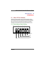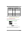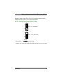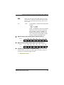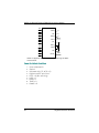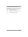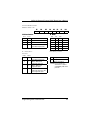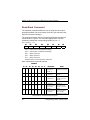
1
AX5411H General Purpose DA&C Board User’s Manual Disclaimers The information in this manual has been carefully checked and is believed to be accurate. AXIOMTEK Co., Ltd. assumes no responsibility for any infringements of patents or other rights of third parties which may result from its use. AXIOMTEK assumes no responsibility for any inaccuracies that may be contained in this document. AXIOMTEK makes no commitment to update or to keep current the information contained in this manual. AXIOMTEK reserves the right to make improvements to this document and/or product at any time and without notice. No part of this document may be reproduced, stored in a retrieval system, or transmitted, in any form or by any means, electronic, mechanical, photocopying, recording, or otherwise, without the prior written permission of AXIOMTEK Co., Ltd. Copyright 2000 by AXIOMTEK Co., Ltd. All rights reserved. January 2000, Version A1 Printed in Taiwan ii Trademarks Acknowledgments AXIOMTEK is a trademark of AXIOMTEK Co., Ltd. IBM is a registered trademark of International Business Machines Corporation. MS-DOS, Windows ’95, Windows NT are trademarks of Microsoft Corporation. TURBO C is a trademark of Borland Inc. BASIC is a trademark of Dartmouth College. Intel is a trademark of Intel Corporation. Other brand names and trademarks are the properties and registered brands of their respective owners. iii ESD Precautions Integrated circuits on computer boards are sensitive to static electricity. To avoid damaging chips from electrostatic discharge, observe the following precautions: ! Do not remove boards or integrated circuits from their anti-static packaging until you are ready to install them. ! Before handling a board or integrated circuit, touch an unpainted portion of the system unit chassis for a few seconds. This helps to discharge any static electricity on your body. ! Wear a wrist-grounding strap, available from most electronic component stores, when handling boards and components. Unpacking The AX5411H is packed in an anti-static bag. The board has components that are easily damaged by static electricity. Do not remove the anti-static wrapping until proper precautions have been taken. Safety instructions in front of this User’s Manual describe anti-static precautions and procedures. After unpacking the board, place it on a raised surface and carefully inspect the board for any damage that might have occurred during shipment. Ground the board and exercise extreme care to prevent damage to the board from static electricity. Integrated circuits will sometimes come out of their sockets during shipment. Examine all integrated circuits to ensure that they are firmly seated. The AX5411H General Purpose DA&C Board package includes the following: # AX5411H Board # AS59099 DAC Driver CD # Cable 20P 31cm (x2) # AX5002 x 1 # AX5411H User‘s Manual # Warranty Card Make sure that all of the items listed above are present. iv What To Do If There Is A Problem If there are damaged or missing parts, contact your supplier and/or dealer immediately. Do not attempt to use the product if there is damage to any of its components. v This page does not contain any information. vi Table of Contents Chapter 1 Introduction 1.1 General Description .......................................... 1 1.1.1 1.2 Accessories Available .................................... 2 Specifications ................................................... 3 Chapter 2 Installation 2.1 Base I/O Port Address 2.1.1 2.2 Full Range Selection ......................................... 8 2.2.1 2.2.2 2.3 2.4 2.5 2.6 7 Base Address Switch Setting .......................... 7 A/D full range selection (JP10) ...................... 8 D/A full range selection (JP6)........................ 9 DMA Channel Selection................................... 10 IRQ Level Selection (JP4) ............................... 10 User Connections ........................................... 11 Hardware Installation ...................................... 14 2.6.1 Board installation: ......................................... 14 Chapter 3 Register Structure & Format 3.1 AX5411H I/O Address MAP.............................. 15 3.1.1 A/D Data Register ( base+0 & base+1 Read Only) 16 Chapter 4 Calibration 4.1 A/D Calibration................................................ 23 Chapter 5 Device Driver 5.1 5.2 General Description ........................................ 25 Programming Technique ................................. 27 5.2.1 5.2.2 5.3 5.4 5.5 TC 2.0 ............................................................. 27 MSC 7.0.......................................................... 28 Function Reference ......................................... 28 More on AXIOMTEK DAC Device Utility (AS59060) ........................................................ 29 Installation ...................................................... 29 Table of Contents vii Appendix A PC I/O Port Mapping Appendix B Block Diagram Appendix C Location Diagram Appendix D Technical Reference Data Acquisition Principles ..................................... 37 Analog Input System ................................................ 37 Analog Output System ............................................. 39 D/A Converter with Double_Buffer ........................... 39 Digital Input and Output........................................... 40 TTL Level I/O Connection ........................................ 40 Digital Input for Open/Short Switch Detecting ..... 40 Digital Input for Large Signal .................................. 40 Digital Output for Relay Driving.............................. 40 Timer and Counter ................................................... 41 Interrupt Operation at DAS ...................................... 41 What you want to know about the interrupt ........ 41 How to use interrupt to transfer data from the AX5411H.................................................................... 42 How to write interrupt routine................................. 42 Appendix E Programming 8254 Timer/Counter Introduction ............................................................. 43 Counter Read/Write and Control Register ................ 44 Read-Back Command ............................................... 46 Counter Operating Mode .......................................... 47 Mode Mode Mode Mode Mode Mode 0 : Interrupt on Terminal Count.................... 47 1 : Hardware Retriggerable One-Shot ........ 47 2 : Rate Generator........................................ 48 3 : Square Wave Mode ................................ 48 4 : Software Triggered Mode ....................... 49 5: Hardware Triggered Strobe Retriggerable 49 Programming Counter/Timer.................................... 50 Example .................................................................... 51 viii Table of Contents AX5411H General Purpose DA&C Board User’s Manual Chapter 1 Introduction 1.1 General Description AX5411H is a multifunction analog/digital input/output board and is functianlly compatible with AX5411. It may also be plugged into one of the available slots in the IBM PC/AT or compatibles. Analog input characteristic of the AX5411H is designed to allow you to sample data at high throughput, the combination of hardware auto-scanning multiplexer, high-speed sample/hold and A/D converter allow input sampling speeds up to 60 KHz. DMA transfer allows you to transfer large amounts of data to memory at such high rate. With programmable gains of 1, 2, 4, 8 and 16, and full scale range of ±5V and ±10V, user can define a particular range for each input corresponding to the signal level connected to that channel. This feature will give optimum resolution to each channel's measurement. Introduction 1 AX5411H General Purpose DA&C Board User’s Manual In addition to the data acquisition channels of AX5411H, the board contains two independent analog voltage output channels. Each channel has its own 12-bit D/A converter. These two channels can be individually set to output a voltage within the range of 0 to 5V or 0 to 10V. The AX5411H also provides a 24 channel digital input port and a 24 channel digital output port. Both ports are TTL compatible. The converted data may be collected through the software command, an interrupt service routine or DMA channels. A complete utility AS59099 DAC Driver CD, containing driver routines and example programs, is furnished with the board to minimize user’s efforts on application software development. These subroutine libraries are available to control AX5411H functions from user written programs. 1.1.1 Accessories Available ! AX750 Low cost screw terminal panel accommodates all analog input connections. Shipped complete with 3.3 foot (1 meter) cable and 50 pin connector. ! AX751 / AX951 Universal screw terminal panel conceived for 50 pin connector wiring conveniently. ! AX752 Table top screw terminal panel designed for thermocouple and low level inputs. Provides differential input for common mode rejection (±10V); Gains of 1, 10, 50, 100 and 1000; Voltage offset and cold-junction compensation; and 8Hz low pass filter. 2 Introduction AX5411H General Purpose DA&C Board User’s Manual 1.2 # Specifications A/D Subsystem ! ! ! ! ! ! ! Number of inputs: Resolution: 16 single-ended 12 bits Sampling Rate: 60KHz max. A/D Conversion Time: 15us max. Channel Acquisition Time: 5us max. System Accuracy: ±0.03% FSR Input Ranges: !10V, !5V, !2.5V, !1.25V, !0.625V, !0.3125V, All ranges software selectable ! Output Coding: Offset binary ! Maximum Input Without Damage # Power On: !30V # Power Off: !45V ! Input Impedance # Off Channel: 100 megohms, 10pF # On Channel: >10 megohms, 50pF ! ! ! ! Nonlinearity: !1 LSB Differential Nonlinearity: Inherent Quantizing Error: !1 LSB !1 LSB Zero Drift: # Bipolar: 17ppm of FSR/C ! Gain Drift: 30ppm of FSR/C ! Monotonicity: Monotonic 0-70C # D/A Subsystem ! ! ! ! ! ! Bias Current: !100nA Number of channels: 2 Output Ranges: 0 to 5V, 0 to 10V Input data coding: Straight binary Current Output, Voltage range: Protection: Introduction +5mA max. Short circuit to Common for voltage ranges, current outputs are short circuit, and reverse polarity protected 3 AX5411H General Purpose DA&C Board User’s Manual # Accuracy ! ! ! ! ! # Resolution: 12bits Nonlinearity: !1 LSB Gain Error: Adjustable to zero Zero Error: Adjustable to zero System Accuracy: !0.025% FSR (voltage out) Dynamic Performance ! Setting Time to 1/2LSB # 10V step: 30us # 5V step: 20us ! Slew Rate: 0.3V/us TYP (voltage) 1.2mA/us (current) ! DAC Throughput # Single Channel: # Thermal Characteristics ! ! ! ! # 33KHz Zero Drift: !10uV/oC Gain Drift: !20ppm of FSR/oC Differential Linearity Drift: !3ppm of FSR/oC Monotonicity: Monotonic, 0 to +70 oC DIO Subsystem ! Digital Input Lines: 24 ! Digital Output Lines: 24 ! Improved Noise Margins: Hysteresis VT+ - VT-=0.4(TYP.) ! Input/Output Level: TTL/DTL Compatible ! Electrical Characteristics: # # # # # # # # 4 VIH: VIL: IIH: IIL: VOH: VOL: IOH: IOL: 2V (MIN.) 0.8V (MAX.) 20uA(MAX.) at VI=2.7V -0.2mA(MAX.) at VIL=0.4V 3.4V(TYP.) at IOH=-0.4mA 0.5V(MAX.) at IOL=8mA -0.4mA (MAX.) 8mA (MAX.) Introduction AX5411H General Purpose DA&C Board User’s Manual # Interface Characteristic ! I/O Connector: one 50-pin and two 20-pin mating header # On-Board Clock ! Base Frequencies: # 4MHz Interface Characteristic ! ! ! ! ! ! Compatible Bus: IBM PC/AT and compatibles ! I/O Bus Interface Type: I/O mapped with 10-bit addressing (A9-A0) Number of Locations Occupied: Data Path: 16 bytes 8 bits Factory Configured Address: 300 Hex Interrupt Options: Software Control to level 2, 3, 4, 5, 6 or 7 Jumper selectable for level 10, 11, 12, 14, 15 ! Interrupt Source: FINISH bit(A/D conversion complete) ! Direct Memory Access Options: Jumper Selectable to DMA1 or DMA3 ! Bus Loading: Presents 1 busload # Power Requirements ! +12Vdc: 40 mA typ. ! -12Vdc: 10 mA typ. ! +5Vdc: 800 mA typ. # Physical/Environmental ! Dimensions: (99H x 165W)mm ! Connector: One 50-pin mating connector Two 20-pin mating connectors ! Operating Temperature Range: 0 oC to 60oC ! Storage Temperature Range: -25 oC to 85oC ! Relative Humidity: To 90%,non-condensing Introduction 5 AX5411H General Purpose DA&C Board User’s Manual This page does not contain any information. 6 AX5411H General Purpose DA&C Board User’s Manual Chapter 2 Installation 2.1 Base I/O Port Address AX5411H will occupy sixteen consecutive I/O port space, setting correct base address by DIP switch to avoid contending other device (refer to appendix A for I/O port distribution). Six bits are equipped to allow you to select the base address from 200(hex) to 3F0(hex). Following Figure illustrates how the I/O port base address is used. 2.1.1 Base Address Switch Setting A 9 8 7 6 5 4 1 2 3 4 5 6 O N Weighting 16 32 64 128 256 512 Installation 7 AX5411H General Purpose DA&C Board User’s Manual I/O Port Range Hexadecimal 000 - 00F 010 - 01F DIP Switch Position 1 2 3 4 5 6 A9 A8 A7 A6 A5 A4 ON ON ON ON ON ON ON ON ON ON ON OFF OFF OFF ON ON ON ON ON ON ON ON ON OFF OFF OFF OFF OFF ON ON ON ON ON ON ON OFF OFF OFF OFF OFF OFF OFF . 200 - 20F 210 - 21F . 300 - 30F(*) 310 - 31F . 3F0 - 3FF NOTE: (*) : Factory Default Setting Address Base Address DIP Switch Setting (SW1) 2.2 Full Range Selection AX5411H furnished 2 jumpers for A/D, D/A full range selection. 2.2.1 A/D full range selection (JP10) 5 5 Range= For + - 5V full-scale For + - 10V full-scale 10 10 Full-scale , Gain=1, 2, 4, 8, 16 Gain When full-scale range selects at ±5V, the available programmable ranges are ±5V, ±2.5V, ±1.25V, ±0.625V and ±0.3125V. 8 Installation AX5411H General Purpose DA&C Board User’s Manual When full-scale range selects at ±10V, the available programmable ranges are ±10V, ±5V, ±2.5V, ±1.25V and ±0.625V. 2.2.2 D/A full range selection (JP6) 5 For +5V full-scale 10 5 For +10V full-scale 10 XXXX D/A output = x Full-scale 4096 XXXX is the 12-bit D/A programmable code range from 0 to 4095 Installation 9 AX5411H General Purpose DA&C Board User’s Manual 2.3 DMA Channel Selection There are two DMA channels can be selected by AX5411H for data transfer. Check your computer status before you use DMA function, avoiding crash the DMA channels each other. JP7 1 DMA CHANNEL 1 3 JP7 1 DMA CHANNEL 3 3 2.4 IRQ Level Selection (JP4) IRQ10 IRQ11 IRQ12 IRQ14 IRQ2~7 selections are via software settings IRQ15 10 Installation AX5411H General Purpose DA&C Board User’s Manual 2.5 User Connections All AX5411H board signals are built in a 50-pin single connector (CN1). It provides an easy and reasonably objective to connect with AX750, AX951 (AX751) or AX752. The CN1 pin assignment is shown below: Name AI0 AI1 AI2 AI3 AI4 AI5 AI6 AI7 AGND +12V NC DA0 AGND DO0 DO1 DO2 DO3 DGND DO4 DO5 DO6 DO7 +5VP EXTRG DGND Pin Pin 1 2 3 4 5 6 7 8 9 10 11 12 13 14 15 16 17 18 19 20 21 22 23 24 25 26 27 28 29 30 31 32 33 34 35 36 37 38 39 40 41 42 43 44 45 46 47 48 49 50 Name AI8 AI9 AI10 AI11 AI12 AI13 AI14 AI15 AGND -12V NC DA1 AGND DI0 DI1 DI2 DI3 DGND DI4 DI5 DI6 DI7 +12VP NC DGND AX5411H (CN1) Pin Assignment Installation 11 AX5411H General Purpose DA&C Board User’s Manual Name I/O Input Output Input Output Source Source Ground Ground Source Source Input AIx DAx DIx DOx + 12V - 12V AGND DGND +5VP +12VP EXTRG NC NOTE: +12V (pin 19) : -12V (pin 20) : +5VP (pin 45) : +12VP (pin 46) : Function Channel x Analog Input D/A Channel x Voltage Output Channel x Digital Input Channel x Digital Output Analog Power Analog Power Analog Ground Digital Ground PC +5V PC +12V External trigger No Connector 600mA max. 600mA max. current limited to PC power current limited to PC power AX5411H also provides two 20-pin connectors (CN2, CN3) for 16-bit digital inputs and 16-bit digital outputs. All these two 20-pin connectors can be connected to the rear plate through the AX5002 industrial wiring kit for a 50-pin mating connector. The pin assignment is shown below: Name +12VP DGND DI23 DI21 DI19 DI17 DI15 DI13 DI11 DI9 Pin Pin 20 19 18 17 16 15 14 13 12 11 10 9 18 7 6 5 4 3 2 1 Name +5VP DGND DI22 DI20 DI18 DI16 DI14 DI12 DI10 DI8 CN2 (Digital Input) Pin Assignment 12 Installation AX5411H General Purpose DA&C Board User’s Manual Name +12VP DGND DO23 DO21 DO19 DO17 DO15 DO13 DO11 DO9 Pin Pin 20 19 18 17 16 15 14 13 12 11 10 9 18 7 6 5 4 3 2 1 Name +5VP DGND DO22 DO20 DO18 DO16 DO14 DO12 DO10 DO8 CN3 (Digital Output) Pin Assignment Name DIx DOx DGND +5VP +12VP Installation I/O Input Output Ground Source Source Function Channel x Digital Input Channel x Digital Output Digital Ground PC +5V PC +12V 13 AX5411H General Purpose DA&C Board User’s Manual 2.6 Hardware Installation The AX5411H board is shipped with protective electrostatic cover. When unpacking, touching the board electrostatically shielded packaging with the metal frame of your computer to discharge the accumulated static electricity prior to touching the board. Following discussing summarizes the procedures for AX5411H installation: WARNING: TURN OFF the PC and all accessories connected to the PC whenever installing or removing any peripheral board including the AX5411H series board. 2.6.1 Board installation: 1. Turn off the PC and all accessories power. 2. Unplug all power cords and entire cables from the rear of the PC. 3. Remove the PC's cover (see your PC Operation Guide if you are not skillful about it) 4. Find a unused expansion slot. Remove the blank expansion slot cover and save the screw for affixing retaining bracket. 5. Grab the upper edge of the AX5411H board. Align the AX5411H board's retaining bracket with the expansion slot rear panel, and straighten the board's gold finger with the expansion slot, crush the board into the slot. 6. Restore the screw in the expansion slot retaining bracket. 7. Replace the PC's cover and connect the cables you detached in step 2. 8. Turn on the PC and other peripheral device power. 14 Installation AX5411H General Purpose DA&C Board User’s Manual Chapter 3 Register Structure & Format 3.1 AX5411H I/O Address MAP AX5411H uses 16 consecutive addresses in I/O space as follows (R = read, W = write): Location Base address + 0 Base address + 1 Base address + 2 Base address + 3 Base address + 4 Base address + 5 Base address + 6 Base address + 7 Base address + 8 Base address + 9 Base address + 10 Base address + 11 Base address + 12 Base address + 13 Base address + 14 Base address + 15 Register Structure & Format Function A/D Low byte Start A/D A/D High byte Gain Control Mux. scan control Digital Input (0~7) Digital Output (0~7) D/A 0 Output Low byte D/A 0 Output High byte D/A 1 Output Low byte D/A 1 Output High byte AX5411H Status Clear interrupt AX5411H Control Digital Input (8~15) Digital Output (8~15) Digital Input (16~23) Digital Output (16~23) 8254 Counter 0 8254 Counter 1 8254 Counter 2 8254 Counter Control Type R W R W R/W R W W W W W R W R/W R W R W R/W R/W R/W W 15 AX5411H General Purpose DA&C Board User’s Manual 3.1.1 A/D Data Register ( base+0 & base+1 Read Only) base 7 6 5 +0 D3 D2 D1 4 3 2 1 0 D0 C3 C2 C1 C0 LSB Bits 0-3 C0-C3 Bits 4-7 D0-D3 base +1 The channel select bits are used to specify one of the 16 channels (0-15) as the input channel for A/D conversions. These bits are A/D least significant data. 7 6 5 4 3 2 1 0 D11 D10 D9 D8 D7 D6 D5 D4 MSB Most Significant A/D data. # Muxtiplexer Scan Register ( base+2 Read/Write) base 7 +2 UC3 6 5 UC2 UC1 End Channel 4 3 UC0 LC3 2 1 0 LC2 LC1 LC0 Start Channel The Mux. scan register is a read/write register that control the channel scan limits of the A/D multiplexer. The high nibble provides the scan ending channel and the low nibble provides the scan starting channel. About 4 microseconds after the A/D starts a conversion, while the sample/hold is holding the previous channel, the multiplexer channel is incremented ready for the next conversion. On finishing the conversion performed with the end channel, the cycle repeats starting with the start channel. On writing to muxtiplexer scan register the counter is always automatically initialized to the start channel. To perform conversions on a single channel, the end and start channel should be made equal to the desired channel number. 16 Register Structure & Format AX5411H General Purpose DA&C Board User’s Manual # # Digital Input DI0~DI7 (base+3 Read Only) base 7 6 5 4 3 2 1 0 +3 DI7 DI6 DI5 DI4 DI3 DI2 DI1 DI0 1 0 Status Functions (base+8 Read Only) base +8 Bits 0-3 Bit 4 Bits 5-6 Bit 7 7 6 5 4 EOC X X INTP 3 2 NC3 NC2 NC1 NC0 NC0-NC3 This the channel number of the next channel to be converted if EOC = 0. The channel changes shorting after EOC goes high and when EOC = 1 may be indeterminate. These status bits provide information on setup for the next conversion. INTP This is the interrupt signal that is directed to interrupt level 2-15 by the control register. If interrupts are disabled INTP = 0. After generation of an interrupt INTP = 1 and will remain high until reset by a write to the Base+8. Your interrupt handler routine should include this write to Base+8 at some point to re-enable the interrupt from AX5411H again. X These bits are don’t care. EOC Indicates the end of a conversion cycle. 0 = conversion has completed; Valid data. 1 = conversion is still in process; Invalid data. A start of A/D conversion will set the EOC=1. Register Structure & Format 17 AX5411H General Purpose DA&C Board User’s Manual # 18 Control Functions (base + 9 Read/Write ) base 7 6 5 4 +9 INTE I2 I1 I0 Bits 0-1 T0-T1 Bit 2 DMAE Bit 3 TRGE Bit 4-6 I0-I2 3 2 TRGE DMAE 1 0 T1 T0 These bits control the source of start pulses for the A/D trigger. T1 T0 Action 0 X Software start only. 1 0 Start on rising of external trig (extrig). 1 1 Start on internal timer trig. X - Meaning don't care Direct memory access transfers are enabled when DMAE = 1 and disabled when DMAE = 0. It is the users responsibility to set up the 8237 DMA controller on the IBM PC system board and the page registers before enabling DMA on AX5411H. External trig (EXTRG) and trig enable (TRGE) of the timer enable register are relative, because TRGE is enable for EXTRG. The relation as following EXTRG TIMER TRGE 0 0 Enable 0 1 Enable 1 0 Disable 1 1 Enable Selects the desired interrupt level for processing interrupts. I1 I0 Interrupt Level I2 0 0 0 Invalid 0 0 1 Enable level 10, 11, 12, 14, 15 0 1 0 Level 2 0 1 1 Level 3 1 0 0 Level 4 1 0 1 Level 5 1 1 0 Level 6 1 1 1 Level 7 Register Structure & Format AX5411H General Purpose DA&C Board User’s Manual NOTE: Bit 7 # +10 This bit enables or disables AX5411H generated interrupts. INTE = 0 – Disable NTE = 1 – Enable If INTE=1 and DMAE=0 an interrupt is generated at the end of each A/D conversion when valid data is available. If INTE=1 and DMAE=1 an interrupt is generated when a termincal count (T/C) is received from the 8237 DMA controller to signify completion of the DMA transfer. 7 6 5 4 3 2 DI15 DI14 DI13 DI12 DI11 DI10 1 0 DI9 DI8 Digital Input DI16~DI23 (base+11 Read Only) base +11 # INTE Digital Input DI8~DI15 (base+10 Read Only) base # When users use JP4 to select IRQ level 10~15, they must set (I2, I1, I0)=(0,0,1). When selecting from IRQ levels 2~7 via software programming, JP4 must be set as OPEN. 7 6 5 4 3 2 DI23 DI22 DI21 DI20 DI19 DI18 1 0 DI7 DI6 Software Start (base + 0 Write Only) A write to base + 0 acts as an A/D trigger and always initiate a conversion on software trigger for A/D. * - Data don't care. Register Structure & Format 19 AX5411H General Purpose DA&C Board User’s Manual # # Gain Control (base + 1 Write Only) base 7 6 5 4 3 2 1 0 +1 X X X X R3 R2 R1 R0 Bits 0-3 R0-R3 Bits 4-7 X Digital Output DO4~DO7 (base+3 Write Only) base +3 # These bits specify the gain. R3 R2 R1 R0 Gain 0 0 0 0 1 0 0 0 1 2 0 0 1 0 4 0 0 1 1 8 0 1 0 0 16 Others are invalid. Don't care 7 6 5 4 3 2 1 0 DO7 DO6 DO5 DO4 DO3 DO2 DO1 DO0 D/A0 Output Registers (base+4 & +5 Write Only) base +4 7 B3 6 B2 5 B1 4 B0 3 X 2 X 1 X 0 X 3 B7 2 B6 1 B5 0 B4 LSB base +5 7 B11 6 B10 5 B9 4 B8 MSB # D/A1 Output Registers (base+6 & +7 Write Only) base +6 7 B3 6 B2 5 B1 4 B0 3 X 2 X 1 X 0 X 3 B7 2 B6 1 B5 0 B4 LSB base +7 7 B11 6 B10 5 B9 4 B8 MSB 20 Register Structure & Format AX5411H General Purpose DA&C Board User’s Manual D/A output registers are write only and in standard low/high byte sequence. Note that the D/A registers are "double buffered" so that the D/As are not updated until the second (high) byte is written. This insures a single step transition on the analog output of D/A. The D/A data format is true binary right justified. # Clear Interrupt (base+8 Write Only) W riting to base + 8 clears AX5411H interrupt request (INTP) and provides the means of acknowledging the AX5411H interrupt and re-enabling it. * - Data don't care. # Digital Output DO8~DO15 (base+10 Write Only) 7 6 5 4 3 2 1 0 DO15 DO14 DO13 DO12 DO11 DO10 DO9 DO8 # Digital Output DO16~DO23 (base+11 Write Only) 7 6 5 4 3 2 1 0 DO23 DO22 DO21 DO20 DO19 DO18 DO17 DO16 # 8254 Programmable Internal Timer(base+12 base+15) Base + 12 Counter 0 Base + 13 Counter 1 Base + 14 Counter 2 Base + 15 Control Onboard the AX5411H, the & 2 are cascaded. Register Structure & Format register register register register counter0 is Read/Write Read/Write Read/Write Write spare and the counters 1 21 AX5411H General Purpose DA&C Board User’s Manual D0 D1 D2 D3 D4 D5 D6 D7 IOR IOW A0 A1 CS CLK0 X G4 X OUT0 CLK1 X 1MHz G1 OUT1 CLK2 G2 OUT2 OUT Refer to Appendix E for details on programming the 8254 timer/counter. Power On Initiate Condition 1. 2. 3. 4. 5. 6. 7. 8. 9. 22 Scan channel=0 Gain=1 Software trig (T1 & T0 = 0) Digital output all of low. EOC = 0 (No A/D trig) INTP = 0 INTE = 0 TRGE = 0 DMAE = 0 Register Structure & Format AX5411H General Purpose DA&C Board User’s Manual Chapter 4 Calibration The AX5411H calibration program (named CAL5411H.exe) provides a menu driven calibration procedure of A/D and D/A. The default I/O port address is at 300(hex). Type CAL5411H to execute the program directly, a 5+1/2 (or better) digit voltage meter and a DC standard (or noise free, stable DC power supply) are necessary. The path of the calibration program is at the AS59099 DAC Driver CD\dac\hardware\ax5411h\ directory. 4.1 A/D Calibration AX5411H A/D calibration includes amplifier offset, A/D offset and full scale, adjustment. Amplifier offset adjustment is executed to lessen input amplifier offset error. A/D offset and full scale adjustment are performed to make sure A/D converter working with the best resolution. Adjustive sequences are as following steps: Step 1 : Step 2 : Step 3 : Step 4 : Step 5 : Step 6 : Step 7 : Calibration Connect a 5+1/2 digital voltage meter (recommend HP3478A) to test point TP2(+) and TP1(-). Select range +/-0.3125V. Connect A/D channel#0 to AGND. Trim VR6 for programmable gain amplifier offset until meter reading less than 0.5mV. Remove meter prob from TP1 and TP2, and set range at +/- 5V. Ground A/D ch#0 and add a 4.9963VDC on ch#1. Consecutively scan A/D ch#0 and ch#1. Trimming VR4 for A/D offset till A/D ch#0 reading equals zero. Trimming VR5 for A/D full scale till A/D ch#1 reading equals the value between 2046 and 2047. Repeat step 6 and 7 until both ch#0 and ch#1 reading in the boundary. 23 AX5411H General Purpose DA&C Board User’s Manual D/A adjustment is executed for AX5411H D/A calibration. The D/A output voltage can be measured by a DVM or directly to the AX5411H A/D input. The sequences are shown below: Step 1 : Step 2 : Step 3 : Step 4 : Step 5 : 24 Connect D/A ch#0, ch#1 to A/D ch#2, ch#3 respectively. Program A/D at +/-5V range on AX5411H. Set jumper JP10 at +5V range, measure D/A channel with a 5+1/2 DVM. Trim VR1 for D/A ch#0 until reading = 4.9988 V. Trim VR2 for D/A ch#1 until reading = 4.9988 V. Calibration AX5411H General Purpose DA&C Board User’s Manual Chapter 5 Device Driver 5.1 General Description The AXIOMTEK DAC Device Driver (AXDDR) provides a set of easy-to-use function calls for our customers to conveniently set up their systems with all AXIOMTEK data acquisition and control devices. Providing almost all source codes in C language, it will essentially help you tune up and debug your applications under DOS environment as well as allow you to fully understand the low level register I/O accompanying those devices. The AXDDR is a part of the AXIOMTEK DAC Device Utility (DevUtil). DevUtil is a diagnostic utility used to diagnose and test the basic functions provided by AXIOMTEK data acquisition and control devices thereby eliminating the necessity to code them. In addition to the AXDDR, some simple demo programs are also available. These demo programs show the correct procedure to call the AXDDR, making the AXIOMTEK data acquisition and control devices work properly. The following table lists the files that you'll find in your driver disk: # DAC\Software\AS59060\…\DEVUTIL\ISA_BUS\ AXDDR\AX5411H> ax5411h.h ax5411h.c ax5411h.txt playtc.bat playmsc.bat turboc.cfg Device Driver $ $ $ $ $ AX5411H device driver header file AX5411H device driver source file AX5411H device driver reference Command line batch file for TC compiler Command line batch file for MSC compiler 25 AX5411H General Purpose DA&C Board User’s Manual # DAC\Software\AS59060\…\DEVUTIL\ISA_BUS\ AXDDR\AX5411H\TC> 5411h_h.obj 5411h_l.obj 5411h_s.obj 5411h_t.obj # 5411h_l.obj 5411h_s.obj 5411h_t.obj misc_l.obj misc_s.obj misc_t.obj $ Additional header file used by AXDDR $ $ $ $ Huge mode object file for TC user Large mode object file for TC user Small mode object file for TC user Tiny mode object file for TC user DAC\Software\AS59060\…\DEVUTIL\ISA_BUS\ AXDDR\MISC\MSC> misc_h.obj misc_l.obj misc_s.obj misc_t.obj tc2msc_h.obj tc2msc_l.obj tc2msc_s.obj tc2msc_t.obj 26 Huge mode object file for MSC user Large mode object file for MSC user Small mode object file for MSC user Tiny mode object file for MSC user DAC\Software\AS59060\…\DEVUTIL\ISA_BUS\ AXDDR\MISC\TC> misc_h.obj # $ $ $ $ DAC\Software\AS59060\…\DEVUTIL\ISA_BUS\ AXDDR\MISC> misc.h # Huge mode object file for TC user Large mode object file for TC user Small mode object file for TC user Tiny mode object file for TC user DAC\Software\AS59060\…\DEVUTIL\ISA_BUS\ AXDDR\AX5411H\MSC> 5411h_h.obj # $ $ $ $ $ $ $ $ $ $ $ $ Huge mode object file for MSC user Large mode object file for MSC user Small mode object file for MSC user Tiny mode object file for MSC user Huge mode object file for MSC user Large mode object file for MSC user Small mode object file for TC user Tiny mode object file for TC user Device Driver AX5411H General Purpose DA&C Board User’s Manual 5.2 Programming Technique There are pre-compiled object files available in AXDDR for both TC and MSC users. If you would like to make your own object files, set up your compiler’s environment first, making sure that you have installed the driver correctly. Use the project file to include all necessary object or library files. The difference between users of TC and MSC are described on the following sections. 5.2.1 TC 2.0 The contents of AXDDR are developed within Turbo C 2.0 IDE (Integrated Development Environment). The config files (*.cfg and *.tc) are for the convenience of TC users. The object files pre-compiled by TC 2.0 compiler can be found under the subdirectory "..\TC". If your version of TC compiler is not compatible with the pre-compiled one, or you want to re-compile your own object file, use the command line batch file, "playtc.bat". You can make your own application that calls the AXDDR driver functions. Simply prepare a project file containing the source file of the application and the object file of your device driver with identical memory model as your application. Don't forget to add the additional object files, "misc_*.obj", to your project file, when using it along with AXDDR. For TC 3.0 users, both config and project files are not compatible to what TC 2.0 uses. To convert the project file of TC 2.0 to TC 3.0, use the utility "prjcnvt.exe" provided by TC 3.0. You can also manually open a new project file and add new items into that project file. Also check for your program's memory model and the directories settings of your TC IDE. The details on using both compiler and linker of TC are not described here. Please refer to the command line batch file, "playtc.bat", or the TC programmer's guide for more detailed information. Device Driver 27 AX5411H General Purpose DA&C Board User’s Manual 5.2.2 MSC 7.0 The pre-compiled object files by MSC compiler can be found in the subdirectory "..\MSC". Use the command line batch file, "playmsc.bat", if to make your own object file. You can make your own application that calls the AXDDR driver functions. After producing an object file of the application, link it with the object file of your device driver and all other required object and library files with the same memory model of that application. Don't forget to add two additional object files, "misc_*.obj" and "tc2msc_*.obj", when using it along with AXDDR. The details on using both compiler and linker of MSC are not described here. Please refer to the command line batch file, "playmsc.bat", or the MSC programmer's guide for more detailed information. 5.3 Function Reference To fully understand and make the most of AXDDR, see the driver function reference file, "ax5411h.txt", found under the same directory containing the device driver source file,"ax5411h.c". Please refer to the reference file before you start using any of the function calls. 28 Device Driver AX5411H General Purpose DA&C Board User’s Manual 5.4 More on AXIOMTEK DAC Device Utility (AS59060) The AXIOMTEK DAC Device Utility (DevUtil), as stated earlier, is an easy-to-use diagnostic utility. It, too, is a demo program that shows the procedure on how to call the AXDDR in sequence. Please consult your local supplier and/or dealer for the availability of DevUtil. 5.5 Installation To build the demo programs of the I/O device, please install the DevUtil first. (DAC\Software\AS59060\Install\Install.exe –d) then copy all the sample files of the I/O device under the same directory as AXDDR, COPY <source files> <target files> For example, COPY E:\DASC\HARDWARE\AX5411H\*.* C:\DEVUTIL\ISA_BUS\DEMO\*.* Device Driver 29 AX5411H General Purpose DA&C Board User’s Manual This page does not contain any information. 30 AX5411H General Purpose DA&C Board User’s Manual Appendix A PC I/O Port Mapping I/O port address range Function 000 - 1FF PC reserved 200 - 20F Game controller (Joystick) 278 - 27F Second parallel print port (LPT2) 2E1 GPIB controller 2F8 - 2FF Second serial port (COM2) 320 - 32F Fixed disk (XT) 378 - 37F Primary parallel print port (LPT1) 380 - 38F SDLC communication port 3B0 - 3BF Monochrome adapter/printer 3C0 - 3CF EGA, reserved 3D0 - 3DF Color/graphics adapter 3F0 - 3F7 Floppy disk controller 3F8 - 3FF Primary serial port (COM1) PC I/O Port Mapping 31 AX5411H General Purpose DA&C Board User’s Manual This page does not contain any information. 32 Block Diagram LC0 LC1 LC2 LC3 WC0 WC1 WC2 WC3 CH15 CH0 Auto-Scan CHANNEL LOGIC MUX. Analog R3 R1 GAIN R2 SPGA VR3 offset (RT0) 20 10 AGND EXT TRG Timer Sft TRG R0 TP2 TP1 VR2 full-scol DMA LOGIC DACK1 DACK3 DRQ3 DRQ1 EOC C0 DB0 C3 DB3 DB4 NC0 NC1 NC2 NC3 INTP 1 0 STATUS EOC Byte Low Byte High REGISTER DB11 INTERRUPT LOGIC W8 clear INTP T0 T1 DMAE TRGE 10 11 12 CONTROL INTE DB0 DB11 VR1 CONVERSION Trig Control LOGIC R/C S/H A/D CONVERTER offset T/C IRQ2 IRQ15 D0 D0 D7 AX5411H General Purpose DA&C Board User’s Manual Appendix B Block Diagram 33 AX5411H General Purpose DA&C Board User’s Manual This page does not contain any information. 34 AX5411H General Purpose DA&C Board User’s Manual Appendix C Location Diagram 2 ON 1 1 19 1 CN3 CN2 19 V R 1 10 11 12 14 15 JP4 V R 2 SW1 3 4 5 6 JP6 V R 4 V R 5 JP7 TP1 JP10 TP2 V R 6 1 49 CN1 Location Diagram 35 AX5411H General Purpose DA&C Board User’s Manual This page does not contain any information. 36 AX5411H General Purpose DA&C Board User’s Manual Appendix D Technical Reference Data Acquisition Principles Factory automation (FA) and laboratory automation (LA) have become a truth tactic owing to the revolution in computer. The advent of the personal computer (PC) makes this task more prevalent and versatile because of the low cost and flexibility. Typically a computerized data acquisition and control system is constructed as following structure: INPUT SIGNAL DA&C SYSTEM COMPUTER (PC) OUTPUT SIGNAL A Basic Based on PC’s Acquisition System Analog Input System The basic function of analog input system (A/D system) is to convert the analog input signal to corresponding digital format that the computer can be read. In order to benefit A/D system's stability and obtain good performance, several other additional parts such as multiplexed, amplifier, sample and hold are required. The following figure exhibits many input signals come into the A/D system. Technical Reference 37 AX5411H General Purpose DA&C Board User’s Manual Signal Conditioning Amplifier INPUT SIGNALS Multiplexed S/H A/D Converter Digital Code A/D converter has several kinds been developed for different application needs. The most widely used A/D converters are integrating and successive approximation. Integrating type has the advantage of high noise rejection but its speed is lower. Most data acquisition system needs at least 12-bit resolution to recognize the measured signal. More high resolution a/d will elapse more time and normally the price is higher. To select suitable specification to meet your need is a good sense. Multiplexed is a device containing a group of switches to select exact channel signal go through A/D converter. Because the amplifier and A/D are shared, the cost will be lower, but the channel's acquisition speed will be reduced too. Sample and hold (S/H) is designed for A/D converter to keep track of input signals. When a high speed A/D converter is used, such as successive approximation, it requires a no changing input signal during the conversion stage. The S/H circuit can keep the input signal with a constant level until the a/d conversion is completed. Often the limiting factor in the application of the S/H is the uncertainty in the time the actual sample is taken - i.e. The "aperture jitter" or Taj. The aperture jitter causes an amplitude uncertainty for any input where the voltage is changing. The approximate voltage error due to aperture jitter depends on the slew rate of the signal at the sample point. 38 Technical Reference AX5411H General Purpose DA&C Board User’s Manual Amplifier is a device to enlarge the input small signal (such as thermocouple, straingage) to a congruous signal that A/D converter can resolvable. Notice if the input signal change is below the A/D system's minimum resolution, the system can not recognize the deviation. The exact gain is usually better the A/D resolution. Analog Output System Analog outputs (digital control analog output D/A) are typically used to generate a programmable level signal for yielding a loop control system. Familiarly analog output range are 0-5v, 0-10v, ±5v, ±10v, 0-20mA, 4-20mA and so on. They can be employed to control such as dc power supply, frequency converter or to drive chart recorders. Normally analog out merely provides little power (voltage output is typical no more than 5mA), power amplifier or current boosters are required attachment when the large load is used. D/A Converter with Double_Buffer A Digital-to-analog (D/A) converter affords an analog output proportional to a digital number on the input. Most converters are 8-, 12-, or even 16-bit, with correspondingly higher resolution. Cost rises rapidly with resolution. Since the analog output change might need be programmed twice (resolution more than 8-bit, needs two byte for one data), SPIKES or GLITCHES (see following figure) are usually engendered to result in control application instability. As a 12-bit D/A, consider the change from 1FF(Hex) to 200(Hex), a 1 LSB step raise. A spike occurs when the high byte is programmed prior to the low byte. Similarly, the low byte is programmed prior to the high byte will form a glitch signal. DOUBLE_BUFFER technique is used at AX5412H to diminish glitches and spikes. When programming the D/A channels, the lower byte should be written first, the 12-bit buffer will keep the result does not be sent to the output until the higher byte is written. Technical Reference 39 AX5411H General Purpose DA&C Board User’s Manual Digital Input and Output Digital signals are usually be used for detecting logical status or controlling devices. TTL level signals are usually developed by most das systems. Some application are showing below: TTL Level I/O Connection VCC R - Slows speed down Increases power dissipation Decreases noise margin Decreases fan-out TTL Devices DO DI CMOS TTL Use pull-up resistor to interface TTL CMOS devices D. GND D. GND Digital Input for Open/Short Switch Detecting +5V * A pull high resistor must be connected to ensure the high level especially at long distance wiring * 4.7K SS Switch SS Digital Input for Large Signal D/I R Digital Output for Relay Driving VCC DI D/O * The D1 is added to protect the IC driver against the inductive "KICKBACK" from the relay coil. 40 Technical Reference AX5411H General Purpose DA&C Board User’s Manual Timer and Counter In many applications precise timers are required to generate a programmable equivalent period pulse for event trigger source. Other applications require to measure count, frequency are also need a counter device. A group of 16-bit down counters are generally applied to achieve these tasks. Intel 8253(or 8254) is a very popular timer/counter IC which contains three separate independent 16-bit down counters. You can program every down counter for a frequency divisor corresponding to it's input clock. AX5412H cascades counter#1 and counter#2 to generate A/D trigger timer from 71.5 minutes per trigger to 2500 KHz. Free counter#0 can be used for event counter or squarewave generator. Interrupt Operation at DAS Most pc-based data acquisitions can benefit from the use of interrupts. The interrupt signal may be occurred from the acquisition hardware to the computer. It can be used to improve data acquisition real response ability with external events. What you want to know about the interrupt PC's family uses intel's 8259A interrupt controller to invoke 8 different interrupt vector service routines. Each vector mapped to software interrupts level 8 through 15 or memory address from 32(hex 20) to 60(hex 40). When an interrupt instruction is executed, the processor saved current both IP(instruction pointer) and CS(code segment) to stack in order to resume when interrupt handler is completed. The interrupt handler routine must be provided to access whatever tasks you required when an interrupt is occurred. The handler routine used registers had to be carefully saved avoiding destroy any previous used data. Technical Reference 41 AX5411H General Purpose DA&C Board User’s Manual How to use interrupt to transfer data from the AX5411H Using interrupt to deal with acquired data is an intellectual strategy. AX5411H utilizes hardware and software abilities to support you to handle interrupt data transfer function. Hardware ability is build on the board (check your PC interrupt channel availability, from level 2 to level 15). Software driver has supported INTR and READ_ST function to access interrupt. How to write interrupt routine Not any routine is provided by the PC's operation system for programming the interrupt controller. In order to use the interrupt effectively and correctly, you must write your interrupt handler as following steps: 42 1. Disable card's control register interrupt bit. 2. Save old interrupt vector. 3. Clear processor interrupt flag. 4. Setup specified interrupt vector. 5. Reset 8259 IMR(interrupt mask register) related bit. 6. Enable card's control register interrupt bit. 7. Set processor interrupt flag. Technical Reference AX5411H General Purpose DA&C Board User’s Manual Appendix E Programming 8254 Timer/Counter Introduction AXIOMTEK's DAS board uses INTEL 8254 as Pacer trigger source, which consist of 3 16-bit counter. The counter 1 and 2 are caseaded and operate as Pacer. The source of counter 1 is attached to switch selectable input frequency (1M or 10MHz). Counter 0 is available for user's special application. Before you start internal pacer, bit 1 & 0 of a register located at address base+9 must be set to 1. There are 2 bit (CLKE, TRGE) used to control Pacer and counter 0, which reside in a register located at address BASE+10 like below: b7 wheras, b6 CLKE:=1 REMARKS: b5 b4 b3 b2 X X X X X X X : don't care TRGE:=1 enable Pacer, otherwise disable b1 b0 CLKE TRGE counter 0 is attached to 100KHz internal input frequency, otherwise attached to external input frequency. AX5210H uses counter 0 through 3 as pacer trigger source. AX5411H: 1. counter 0 is spare 2. TRGE is at bit 3 of register located at address Base+9 3. have no CLKE Programming 8254 Timer/Counter 43 AX5411H General Purpose DA&C Board User’s Manual Counter Read/Write and Control Register There are 4 register needed to program 8254 Timer/Counter, including 3 Read/Write and 1 control register located a dress. Base+12 through Base+15: Base+12 Base+13 Base+14 Base+15 counter 0 Read/Write register counter 1 Read/Write register counter 2 Read/Write register control word register Read/Write register is used to load divisor to select counter, or Read count from selected counter. Control register is used to determine counter's operation. 44 Programming 8254 Timer/Counter AX5411H General Purpose DA&C Board User’s Manual Control Word Format Address base +15 D7 D6 D5 D4 D3 D2 D1 D0 SC1 SC0 RW1 RW0 M2 M1 M0 BCD SC Select Counter: SC1 SC0 0 0 0 1 1 0 1 1 RW0 0 0 0 1 0 1 1 M2 M1 0 0 0 Select Counter 0. Select Counter 1. Select Counter 2. Read-Back Command (See Read Operations). W – Read/Write: Decimal: RW1 M - MODE: Counter Latch Command (See Read Operations). Read / Write least significant byte only. Read / Write most significant byte. Read / Write least significant byte first, then most significant byte. Programming 8254 Timer/Counter M0 0 1 1 X 0 0 X 1 1 1 0 0 1 0 1 Mode0 Mode1 Mode2 Mode3 Mode4 Mode5 BCD-Binary Coded Binary Counter 16-Bit Binary Coded Decimal (BCD) (4 Decades) NOTE: Don‘t Care bits (X) should be 0 to insure compatibility with future products. 0 1 45 AX5411H General Purpose DA&C Board User’s Manual Read-Back Command The read-back command allows the user to check the count value, programmed Mode, and current state of the OUT pin and Null Count flag of the selected counter(s). The command is written into the Control Word Register and has the format shown is Figure 8. The command applies to the counters selected by setting their corresponding bits D3, D2, D1 = 1. Base Address + 15 D7 D6 D5 D4 D3 D2 D1 D0 1 1 COUNT STATUS CNT 2 CNT 1 CNT 0 0 D5: 0 = Latch count of selected Counters(s) D4: 0 = Latch status of selected Counters(s) D3: 1 = Select Counter 2 D2: 1 = Select Counter 1 D1: 1 = Select Counter 0 D0:Reserved for future expansion, Must be 0 Here is Read-back command example: Command D7 D6 D5 D4 D3 D2 D1 D Description Result 1 1 0 0 0 0 1 0 Read back count and status of Counter 0 Count and status latched for Counter 0 1 1 1 0 0 1 0 0 Read-back status of Counter 1 Status latched for Counter 1 1 1 1 0 1 1 0 0 Read-back status of Counter 2, 1 Status latched for Counter 2, cut not Counter 1 1 1 0 1 1 0 0 0 Read-back count of Counter 2 Count latched for Counter 2 1 1 0 0 0 1 0 0 Read-back count and status of Counter 1 Count latched for Counter 1, but not status 1 1 1 0 0 0 1 0 Read-back status of Counter 1 Command ignored, status already latched for Counter1 Read-Back Command Example 46 Programming 8254 Timer/Counter AX5411H General Purpose DA&C Board User’s Manual Counter Operating Mode Mode 0 : Interrupt on Terminal Count Mode 0 is typically used for event counting. After the Control Word is written, OUT is initially low, and will remain low until the Counter reaches Zero. OUT then goes high and remains high until a new count or a new Mode 0 Control Word is written to the Counter. GATE = 1 enables counting; GATE = 0 disables counting. GATE has no effect on OUT. After the Control Word and initial count are written to a Counter, the initial count will be loaded on the next CLK pulse. This CLK pulse does not decrement the count, so for an initial count of N, OUT does not go high until N + 1 CLK pulses after the initial count is written. If a new count is written to the Counter it will be loaded on the next CLK pulse and counting will continue form the new count. If a two-byte count is written, the following happens : 1. Writing the first byte disables counting. Out is set low immediately (no clock pulse required). 2. Writing the second byte allows the new count to be loaded on next CLK pulse. Mode 1 : Hardware Retriggerable One-Shot OUT will be initially high. OUT will go low on the CLK pulse following a trigger to begin the one-shot pulse, and will remain low until the Counter reaches zero. OUT will then go high and remain high until the CLK pulse after the next trigger. After writing the Control Word and initial count, the Counter is armed. A trigger results in loading the Counter and setting OUT low on the next CLK pulse, thus starting the one-shot pulse N CLK cycles in duration. The one-short pulse can be repeated without rewriting the same count into the counter. GATE has no effect on OUT. Programming 8254 Timer/Counter 47 AX5411H General Purpose DA&C Board User’s Manual If a new count is written to the Counter during a one-short pulse, the current one-shot is not affected unless the Counter is retriggered. In that case, the Counter is loaded with the new count and the one-shot pulse continues until the new count expires. Mode 2 : Rate Generator This Mode functions like a divide-by-N counter. It is typically used to generate a Real Time Clock interrupt. OUT will initially be high. When the initial count has decremented to 1, OUT goes low for one CLK pulse. OUT the goes high again, the Counter reloads the initial count and the process is repeated Mode 2 is periodic; the same sequence is repeated indefinitely. For an initial count of N, the sequence repeats every N CLK cycles. After writing a Control Word and initial count, the Counter will be loaded on the next CLK pulse. OUT goes low N CLK pulses after the initial count is written. This allows the Counter to be synchronized by software also. Mode 3 : Square Wave Mode Mode 3 is typically used for Baud rate generation. Mode 3 is similar to Mode 2 except for the duty cycle of OUT. OUT will initial be high. When half the initial count has expired, OUT goes low for the remainder of the count. Mode 3 is periodic; the sequence above is repeated indefinitely. An initial count of N results in a square wave with a period of N CLK cycles. After writing a Control Word and initial count, the Counter will be loaded on the next CLK pulse. This allows the Counter to be synchronized by software also. Mode 3 is implemented as follows: EVEN COUNTS: OUT is initially high. The initial count is loaded on one CLK pulse and then is decremented by two on succeeding CLK pulses. When the count expires, OUT changes value and the Counter is reloaded with the initial count. The above process is repeated indefinitely. 48 Programming 8254 Timer/Counter AX5411H General Purpose DA&C Board User’s Manual ODD COUNTS: OUT is initially high. The initial count is loaded on one CLK pulse, decremented by one on the next CLK pulse, and then decremented by two on succeeding CLK pulses. When the count expires, OUT goes low and the Counter is reloaded with the initial count. The count is decremented by three on the next CLK pulse, and then by two on succeeding CLK pulses. When the count expires, OUT goes high again and the Counter is reloaded with the initial count. The above process is repeated indefinitely. So for odd counts, OUT will be high for (N + 1)/2 counts and low for (N -1)/2 counts. Mode 4 : Software Triggered Mode OUT will be initially high. When the initial count expires, OUT will go low for one CLK pulse then go high again. The counting sequence is "Triggered" by writing the initial count. After writing a Control Word and initial count, the Counter will be loaded on the next CLK pulse. This CLK pulse does not decrement the count, so for an initial count of N, OUT does not strobe low until N + 1 CLK pulses after the initial count is written. If a new count is written during counting, it will be loaded on the next CLK pulse and counting will continue form the new count. If a two-byte count is written, the following happens: 1. Writing the first byte has no effect on counting. 2. Writing the second byte allows the new count to be loaded on the next CLK pulse. This allows the sequence to be "retriggered" by software OUT strobes low N + 1 CLK pulses after the new count of N is written. Mode 5: Hardware Triggered Strobe Retriggerable OUT will initially be high. Counting is triggered by a rising edge of GATE. When the initial count has expired, OUT will go low for one CLK pulse and then go high again. Programming 8254 Timer/Counter 49 AX5411H General Purpose DA&C Board User’s Manual Programming Counter/Timer Programming Sequence: 1. Writing control word to select counter and determine operation. 2. Program selected counter's LSB of R/W register. 3. Program selected counter's MSB of R/W register. Control Word LSB of count MSB of count Control Word LSB of count MSB of count Control Word LSB of count MSB of count Base Address + - Counter 0 - Counter 0 - Counter 0 - Counter 1 - Counter 1 - Counter 1 - Counter 2 - Counter 2 - Counter 2 15 12 12 15 13 13 15 14 14 Control Word Control Word Control Word LSB of count MSB of count LSB of count MSB of count LSB of count MSB of count Base Address - Counter - Counter - Counter - Counter - Counter - Counter - Counter - Counter - Counter Control Word Control Word Control Word LSB of count LSB of count LSB of count LSB of count MSB of count MSB of count - 15 15 15 14 13 12 12 13 14 Control Word Control Word LSB of count Control Word LSB of count MSB of count LSB of count MSB of count MSB of count - NOTE: Counter Counter Counter Counter Counter Counter Counter Counter Counter 0 1 2 2 1 0 0 1 2 Counter Counter Counter Counter Counter Counter Counter Counter Counter + 2 1 0 2 2 1 1 0 0 15 15 15 14 14 13 13 12 12 1 0 1 2 0 1 2 0 2 15 15 13 15 12 13 14 12 14 In all four examples, all counters are programmed to Read/Write two-byte count is. These are only four programming sequences among the many others possible. A Few Possible Programming Sequences 50 Programming 8254 Timer/Counter AX5411H General Purpose DA&C Board User’s Manual Example # Example 1 10 20 30 40 50 60 70 80 # Program counter 0 as rate generator Divisor%=100 LSB%=Divisor% MOD 256 MSB%=Divisor%\256 Base%=&H300 OUT Base%+10, &H02 ' enable internal 100K Hz input ' frequency OUT Base%+10, &H34 ' counter 0: rate generator OUT Base%+12, LSB% ' write low byte to counter 0 'R/W register OUT Base%+12, MSB% ' write high byte Example 2 Read count of counter 0 10 Base%=&H300 20 OUT Base%+15, 0 ' Latch counter 0 30 LSB%=inp(Base%+12) ' Read low byte 40 MSB%=inp(Base%+12) ' Read high byte 50 Count%=LSB%+MSB%*256 ' count of counter 0 Programming 8254 Timer/Counter 51 AX5411H General Purpose DA&C Board User’s Manual This page does not contain any information. 52