1
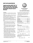
NCL30000LED2GEVB 180-265 Vac up to 15 Watt Dimmable LED Driver Evaluation Board User's Manual http://onsemi.com EVAL BOARD USER’S MANUAL Introduction This manual also focuses on how the board can be modified to support alternate output currents and power levels. The NCL30000 datasheet contains additional information on operation of the controller and LED driver application. Application Note AND8451 details power stage design details and AND8448 provides specific information for dimming applications. Design calculations are covered in greater detail in these documents. The compact evaluation board is constructed with through-hole components on the top and surface mount components on the bottom side. This board was designed to meet safety agency requirements but has not been evaluated for compliance. When operating this board, observe standard safe working practices. High voltages are present on the board and caution should be exercised when handling or probing various points to avoid personal injury or damage to the unit. Figures 1 and 2 show the top and bottom sides of this evaluation board. AC input connects to the terminal block in the upper left corner. Terminals are marked “L” and “N” for Line and Neutral. The LED load connects to the terminal block in the upper right corner. Note the board is labeled “LED+” and “LED−“. Observe polarity when connecting LED loads. Never connect LEDs to the driver while it is running or before the output capacitors discharge after removing input power. In open load conditions the output capacitors charge to >56 volts. Energy stored in the output capacitance can damage or shorten the effective life of the LEDs if improperly discharged into the LEDs. The NCL30000 is a power factor corrected LED driver controller. This evaluation board manual describes the setup and operation of the NCL30000LED2GEVB LED driver for 230 V input. The evaluation board implements an isolated single stage Critical conduction Mode (CrM) flyback converter providing a regulated constant current to an LED load. This board has been specifically configured to support leading and trailing edge line dimming and has been characterized across a range of commercially available dimmers. The output voltage range is suitable for nominal 4 to 15 high brightness power LEDs. Protection features include open load protection, over temperature protection, and overload limiting. As shipped, the evaluation board is set up for the following parameters: Evaluation Board Specifications Input Voltage Range: 180 − 265 Vac Output Current: 350 mA 5% Output Voltage Range: 12 − 50 Vdc Output Power: up to 17.5 W Full Load Efficiency: >82% Power Factor: >0.93 Typical 50C Ambient Operation Class B Conducted Emissions Compatible with Triac and Electronic Dimmers Semiconductor Components Industries, LLC, 2012 September, 2012 − Rev. 2 1 Publication Order Number: EVBUM2100/D NCL30000LED2GEVB Figure 1. Top Side of Board Figure 2. Bottom Side of Board http://onsemi.com 2 NCL30000LED2GEVB Figure 3. Board Schematic http://onsemi.com 3 NCL30000LED2GEVB Board Configuration On-time Capacitor The evaluation board has been optimized for dimming with a 12 W load. Output current is regulated at 350 mA from 265 V rms down to a setpoint of about 200 V rms. When the input voltage is ~200 V rms, the control method changes from closed loop secondary side current control to primary side control. As the input voltage is reduced further the output current drops in a smooth fashion in response to the lower input voltage. This response matches the driver to a dimmer thus emulating the dimming response of an incandescent bulb. The following information details reconfiguring the evaluation board for alternate applications. The input voltage at which dimming or reduction of output current occurs is controlled by C9, power delivered to the LED load, and parameters from the evaluation board. The approximate value of C9 is calculated by the formula below: C9 [ 4 @ L pri @ P out @ I charge hȀ @ V 2 pk @ V Ctmax @ ǒ V pk N @ V out Ǔ )1 (eq. 1) Values in the equation above are described in Table 1 below: Table 1. VARIABLES FOR CALCULATING CT CAPACITOR Variable Description Lpri Transformer Primary Inductance Pout Power Output to LEDs Icharge h’ Vpk Vctmax N Vout Value for Evaluation Board 0.00157 12 Nominal On Time Capacitor Charge Current 275 mA Transformer/Secondary Efficiency 0.95 Dimming Point Peak Voltage 200 Vrms = 282.8 Vpk Nominal On Time Capacitor Peak Voltage 4.93 Transformer Turns Ratio 3.83 LED Load Voltage (12 LEDs) C9 [ 37 4 @ 0.00157 @ 12 @ 275m 0.95 @ 282.8 2 @ 4.93 @ 282.8 ) 1Ǔ + 166 pF ǒ3.83 @ 37 (eq. 2) Output Current Setup In practice, the value of capacitance calculated is an approximation of operating conditions and optimization is required. Empirical testing with a dimmer may be done to select the optimum input voltage for dimming to begin. A value of 180 pF was selected for C9 on the evaluation board to achieve desired results. Modifying this evaluation board for alternate LED configurations and power levels is straight forward. Using the equation above, enter the target LED power, LED voltage, and the target AC input voltage below which dimming should occur. Select a capacitor somewhat below the value returned by the approximate formula. Performance should be evaluated using the desired dimmers. Check operation by noting the conduction angle below which LED current reduces. Increasing the value of capacitor C9 lowers the conduction angle where dimming occurs. Performance can be optimized by selecting the value of C9. Figure 4 below is the bottom side of the evaluation board. Component locations are circled indicating those values that are most likely to be changed to optimize for a different power level. A particular driver application may require LED current other than 350 mA. Output current is controlled by R29 located in Figure 4. The following formula is used to set the output current. R29 + 0.07 I out (eq. 3) Dissipation for current sense resistor R29 is defined by the formula below. P R29 + 0.07 R29 2 (eq. 4) The secondary windings of power transformer T1 are connected in series to support the 50 V/350 mA output rating of the evaluation board. Applications below 25 V or greater than 450 mA output should have the transformer secondary windings configured in parallel. This helps maintain proper primary bias voltage and enhances current carrying capability of the transformer. Table 2 shows how to configure the transformer flying leads in the PCB holes for series and parallel configuration. Figure 5 is the top side of the circuit board highlighting the wire holes H1 − H6. Table 2. WINDING CONFIGURATION Winding Configuration H1 H2 H3 H4 H5 H6 Series (default) FL1 <open> FL2 FL3 <open> FL4 Parallel FL1 FL3 <open> <open> FL2 FL4 http://onsemi.com 4 NCL30000LED2GEVB Figure 4. Bottom Side PCB Component Locations Figure 5. PCB Holes for Transformer Leads http://onsemi.com 5 NCL30000LED2GEVB Primary Current Limit As built, the evaluation board is suitable for 17.5 W maximum. The transformer secondary windings will support up to 1 A of LED current with secondary windings configured in parallel. A 300 V output rectifier was selected for applications up to 50 Vdc output and 265 V ac input. Lower voltage rectifiers are recommended for applications below 50 Vdc. A lower forward voltage drop output rectifier will improve efficiency. Selecting a rectifier with a higher current rating typically provides lower forward drop at the currents of interest. A 3 A rectifier was selected for the evaluation board to provide low forward drop. Any change to the output rectifier requires verifying the maximum voltage rating is not exceeded. Maximum current in the switching FET Q3 is established by R20. The demo board components have been designed to support up to 17.5 W output at 180 V rms input. Note C9 has been preconfigured for 180 pF which limits the maximum power. If the application requires alternate power level or input voltage, the value of R20 can be adjusted. Lower power or high input line voltage applications my benefit from a higher value resistance which provides cycle-by-cycle current monitoring in the event of a fault. The formula below provides an estimated value for R20 which includes a 25% tolerance for components and start up conditions. R20 + Output Capacitor The evaluation board regulates constant current and therefore the output voltage is determined by the LED load characteristics at the set current level. Energy storage to maintain high power factor and low output ripple current requires relatively large output filter capacitors. The LED load can be modeled as a constant voltage source with some series impedance. In essence, the ripple current in the LEDs is controlled by the series impedance coupling the constant voltage nature of the filter capacitance and constant voltage characteristic of the LEDs in a complex relationship. Two 470 mF capacitors connected in parallel provide about 30% or 105 mA peak-to-peak ripple for a 350 mA average LED current. Increasing the output capacitance reduces the ripple current and conversely decreasing capacitance will increase the ripple. Applications requiring average output currents other than 350 mA can be scaled to this value. For example an application requiring 700 mA requires two 1,000 mF capacitors in parallel to provide 30% ripple. 0.5 1.25 @ I pri (eq. 5) Open Load Protection The evaluation board includes a circuit to protect the output capacitors in the event of open load conditions. The output voltage will be limited when zener diode D12 exceeds the zener voltage plus ~0.7 V. D12 is presently 56 V which means the maximum output will be approximately 56.7 V. D12 can be changed to protect output capacitors of different voltage rating. Select D12 zener voltage to match open load requirements. The location of D12 is shown in Figure 4. Typical Performance Data Figure 6 below displays the relationship between input voltage and LED current for a 12 LED, 13 W load. Higher input voltages allow the secondary side control loop to regulate 350 mA output current at 37 V nominal load. Note the inflection point where reduction in current begins as the input voltage is reduced below 200 Vac. This is the dimming inception point. http://onsemi.com 6 350 100% 315 90% 280 80% 245 70% 210 60% 175 50% 140 40% 105 30% 70 20% LED Current Efficiency 35 0 30 50 70 90 110 130 150 170 Input Voltage (Vac) 190 210 230 250 Efficiency LED Current (mA) NCL30000LED2GEVB 10% 0% 270 Figure 6. Line Regulation and Efficiency for 13 W Load load at 230 Vac, 50 Hz input and applicable limits are shown in Table 3. Efficiency performance is shown in Figure 6 as well. Note the efficiency remains above 70% until the output current drops below 70 mA. The output voltage is about 34 V meaning the delivered power is about 2.4 W or less than 20% of the full power. As the current delivered is reduced, the fixed losses for startup and biasing begin to dominate the efficiency curve resulting in a steep drop off of efficiency. Harmonic content characterizes the waveshape of the input current waveform. Odd order harmonics of the fundamental distort the input waveform resulting in non-sinusoidal shape. International standard IEC 61000−3−2 Class C places limits on input current harmonics for lighting equipment. A category for devices drawing not more than 25 W applies to this reference design. Performance of this demonstration board with a 12 W LED Table 3. INPUT CURRENT HARMONIC CONTENT Harmonic Value Limit 3 11.02% 86% 5 5.16% 61% Power factor and input current Total Harmonic Distortion (THD) are performance factors receiving considerable attention from utility companies and government agencies. Figure 7 below displays performance of the evaluation board. The EMI filter was designed for a 17.5 W load. The filter can be optimized for higher power factor in applications requiring less power. http://onsemi.com 7 20 0.98 19 0.97 18 0.96 17 0.95 16 0.94 15 0.93 14 0.92 13 0.91 THD Power Factor 12 0.9 11 10 Power Factor (PF) Percent Input Current THD (%) NCL30000LED2GEVB 0.89 180 195 210 225 Input Voltage (Vac) 240 0.88 270 255 Figure 7. Power Factor and THD of greater than 10:1 was consistently demonstrated. Note that minimum conduction angle and therefore LED current is controlled by the design of the triac or electronic dimmer selected. The evaluation board was tested with a variety of commercial dimmers. Figure 8 shows the dimming performance with several triac and electronic dimmers. Dimming control range varies by manufacturer, but a range 385 350 315 280 LED Current (mA) 245 210 Lutron LLSM−502 Clipsal KB31RD400 MK SX8501 Clipsal 32V500 Alombard 741021 Legrande Celiane Clipsal 32E450UD Clipsal 32E450LM 175 140 105 70 35 0 0 20 40 60 80 100 Conduction Angle (degrees) 120 Figure 8. Performance of Evaluation Board with Various Line Dimmers http://onsemi.com 8 140 160 NCL30000LED2GEVB Table 4 lists commercial dimmers successfully tested with the evaluation board. The load is 12 LEDs (Vf = 37 Vdc) and nominal current is set for 350 mA. Table 4. DIMMER COMPATIBILITY CHART Manufacturer Minimum Conduction Angle (degrees) Dimmer Model Current at Minimum Conduction Angle (mA) Alombard 741021 20.7 7.2 Clipsal KB31RD400 38.2 55.2 Clipsal 32E450LM 10.6 1 Clipsal 32E450UD 30.8 29.5 Clipsal 32V500 9.2 0 Legrande 999.58 18 23.8 Lutron LLSM−502 27.4 25.7 MK SX8501 41.8 74 Conclusion Additional Application Information and Tools The NCL30000LED2GEVB is a versatile dimmercompatible LED driver. This board provides rapid assessment of capabilities and serves as a basis for LED driver solutions. Smooth flicker-free dimming performance is demonstrated with a wide variety of commercially available dimmers. Full 350 mA LED current is provided at maximum dimmer setting. High power factor and high efficiency provide a cost effective solution for a dimmer compatible LED driver. The NCL30000LED2GEVB evaluation board, NCL30000 datasheet, AND8451 Power Stage Design Guidelines, Microsoft Excel Design Spreadsheet, and AND8448 TRIAC Dimming application note are available at www.onsemi.com. Microsoft and Excel are registered trademarks of Microsoft Corporation. ON Semiconductor and are registered trademarks of Semiconductor Components Industries, LLC (SCILLC). SCILLC owns the rights to a number of patents, trademarks, copyrights, trade secrets, and other intellectual property. A listing of SCILLC’s product/patent coverage may be accessed at www.onsemi.com/site/pdf/Patent−Marking.pdf. SCILLC reserves the right to make changes without further notice to any products herein. SCILLC makes no warranty, representation or guarantee regarding the suitability of its products for any particular purpose, nor does SCILLC assume any liability arising out of the application or use of any product or circuit, and specifically disclaims any and all liability, including without limitation special, consequential or incidental damages. “Typical” parameters which may be provided in SCILLC data sheets and/or specifications can and do vary in different applications and actual performance may vary over time. All operating parameters, including “Typicals” must be validated for each customer application by customer’s technical experts. SCILLC does not convey any license under its patent rights nor the rights of others. SCILLC products are not designed, intended, or authorized for use as components in systems intended for surgical implant into the body, or other applications intended to support or sustain life, or for any other application in which the failure of the SCILLC product could create a situation where personal injury or death may occur. Should Buyer purchase or use SCILLC products for any such unintended or unauthorized application, Buyer shall indemnify and hold SCILLC and its officers, employees, subsidiaries, affiliates, and distributors harmless against all claims, costs, damages, and expenses, and reasonable attorney fees arising out of, directly or indirectly, any claim of personal injury or death associated with such unintended or unauthorized use, even if such claim alleges that SCILLC was negligent regarding the design or manufacture of the part. SCILLC is an Equal Opportunity/Affirmative Action Employer. This literature is subject to all applicable copyright laws and is not for resale in any manner. PUBLICATION ORDERING INFORMATION LITERATURE FULFILLMENT: Literature Distribution Center for ON Semiconductor P.O. Box 5163, Denver, Colorado 80217 USA Phone: 303−675−2175 or 800−344−3860 Toll Free USA/Canada Fax: 303−675−2176 or 800−344−3867 Toll Free USA/Canada Email: [email protected] N. American Technical Support: 800−282−9855 Toll Free USA/Canada Europe, Middle East and Africa Technical Support: Phone: 421 33 790 2910 Japan Customer Focus Center Phone: 81−3−5817−1050 http://onsemi.com 9 ON Semiconductor Website: www.onsemi.com Order Literature: http://www.onsemi.com/orderlit For additional information, please contact your local Sales Representative EVBUM2100/D