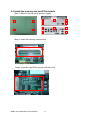
1
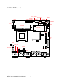
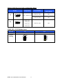
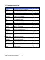
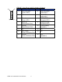
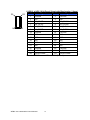
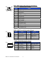
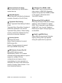
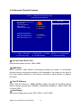
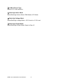
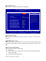
WFBX-1011-5256 User Manual Rev.01, May. 2012 Statement All rights reserved. No part of this publication may be reproduced in any forms or by any means, without prior written permission of the publisher. All trademarks are the properties of the respective owners. All product specifications are subject to change without prior notice Packing List 1. WFBX-1011-5256 x 1 2. 60W DC12V Screw type adapter x 1 3. Y-cable x 1 4. Power cord x 1 5. Foot pad x 4 6. Screws pack x 1 7. Wall mount kit x 1 8. Driver CD (Include user’s manual) x 1 Ordering Information STANDARD: □ WFBX-1011-5256 Fanless-BOX PC with Atom D525 CPU with 1xVGA, 6xCOM, 1xLPT, 2xLAN, 8xUSB, 1xPS2, 1xAudio(Mic-in, Audio out), 1xDDR3 204PIN SODIMM max up to 4GB, CF and 2.5" HDD support, wall mount kit, 60W DC12V Screw type adapter. WFBX-1011-5256 series User’s Manual 2 Contents Chapter 1 Product Information .......................................................................................... 4 1.1 General Description ................................................................................................... 4 1.2 Features ........................................................................................................................ 5 1.3 Dimensions .................................................................................................................. 6 1.4 I/O Outlets..................................................................................................................... 7 1.5 M/B PCB Layout .......................................................................................................... 9 1.6 Jumper Setting .......................................................................................................... 10 1.7 Connector Function List......................................................................................... 14 1.8 Internal Connector Pin Define............................................................................... 15 Chapter 2 Hardware installation ..................................................................................... 22 2.1 Installing the Wall mount kit .................................................................................. 22 2.2 Installing the Foot pad ............................................................................................ 22 2.3 Installing the 2.5” HDD and CF module .............................................................. 22 2.4 Installing the memory and miniPCIe module .................................................... 24 Chapter 3 BIOS Setup ........................................................................................................ 25 3.1 Main Menu .................................................................................................................. 25 Chapter 4 Drivers Installation .......................................................................................... 50 4.1 Intel Chipset Device Software ............................................................................... 50 4.2 Intel Graphic Media Accelerator Driver .............................................................. 53 4.3 LAN Driver .................................................................................................................. 56 4.4 Audio Driver ............................................................................................................... 58 Appendix-A Watchdog ....................................................................................................... 59 Appendix-B GPIO ................................................................................................................ 61 WFBX-1011-5256 series User’s Manual 3 Chapter 1 Product Information This chapter introduces the product features, jumper and connector information. 1.1 General Description WFBX-1011-5256 is Fanless BOX PC system that can support Atom D525 dual core processor. The WFBX-1011-5256 support Windows® 2000, Windows® XP, Windows® XP embedded, Windows® 7, suitable for the most endurable operation. WFBX-1011-5256 series User’s Manual 4 1.2 Features Construction Heave duty steel CPU Intel Atom D525 Dual core 1.8GHz processor onboard System memory 1 x 204-pin DDR3 800 SO DIMM SDRAM, max. up to 4GB Chipset Intel D525 + ICH8M BIOS Award 16MB SPI System I/O Front I/O: 2 x USB Rear I/O: 6 x USB, 2 x LAN, 1 x VGA, 1 x PS2, 1 x LPT 6 x COM(5 x RS-232, 1 x RS-232/422/485); All COM with +5V/+12V/RI support by jumper selector 1 x Audio(Mic-in, Audio-out), Watch dog timer Interval: Programmable 1~255 sec. Storage support 1 x CF and 1 x 2.5" HDD Expansion slot 1 x mini-PCIe System Indicators 1 x Power LED, 1 x HDD LED System controls 1 x Power on switch Mounting Kit Wall mount kit Power Supply AC 60W Screw type adapter, Input: AC 100~240V/50-60Hz, Output: DC12V@5A Operating Temperature 0°C~50°C (32°F~122°F) Storage temperature -20°C~80°C (-68°F~176°F) Relative Humidity 0%~90% (non-condensing) Dimensions 260mm(W) x 209.2mm(D) x 73mm(H) 10.2"(W) x 8.23"(D) x 2.87"(H) Weight Gross: 4.96Kg/10.93Lb Net: 4.35Kg/9.59Lb Standard Color Sliver WFBX-1011-5256 series User’s Manual 5 1.3 Dimensions The following diagrams show you dimensions and outlines of WFBX-1011-5256. WFBX-1011-5256 series User’s Manual 6 1.4 I/O Outlets FRONT 1 1. 2. 3. 4. USB (2 PORTS) HDD status LED Power status LED Power on button WFBX-1011-5256 series User’s Manual 7 2 3 4 BACK 15 16 17 18 19 5 6 7 8 9 5. DC12V input 6. COM Port (COM1) 7. USB Port (2 port) 8. VGA Port 9. USB Port (2 port) 10. USB Port (2 port) 11. Print Port 12. Audio (Mic-in) 13. COM Port (COM4) 14. COM Port (COM5) WFBX-1011-5256 series User’s Manual 20 10 11 21 22 12 23 13 14 15. SMA hole 16. COM Port (COM2) 17. PS2 (Keyboard/Mouse) 18. COM Port (COM3) 19. LAN1 20. LAN2 21. Audio (Line-out) 22. SMA hole 23. COM Port (COM6) 24. SMA hole 8 24 1.5 M/B PCB Layout SATA_PWR1 3 1 4 7 4 1 7 JPWR_SEL 29 1 1 1 4 2 SATA2 1 SATA1 30 4 JLVDS JCMOS SYSFAN1 SATA_PWR2 JMODE0 JMODE1 LVDS18 JMODE2 COM6 JCOM6 JCOM5 1 5 2 5 10 INV 2 10 1 5 COM5 5 2 2 6 6 1 29 1 2 9 SO - DIMM1 JCOM4 10 30 1 9 9 1 6 2 1 MINI- PCIE COM4 16 JPCI-E 15 1 2 LVDS24 USB4 10 JFRONT 7 1 9 2 1 2 1 2 14 10 LPC 1 JIDE JCF 2 7 LPT JSPI JCOM2_SEL 1 4 3 2 PWR1 26 1 13 8 JCOM1 JCOM3 PCIE4 RT1 AUDIO2 1 5 JCOM2 2 10 1 2 6 11 1 1 USB1_KBMS COM1_COM2 USB_LAN1 VGA_COM3 WFBX-1011-5256 series User’s Manual 9 1 2 10 6 2 9 6 1 2 VGA2 5 23 24 6 MCR 2 5 1 4 CPUFAN1 USB_LAN2 DIO1 AUDIO1 1.6 Jumper Setting JCMOS: CMOS Clear Pin No. Function 1-2 2-3 Normal Operation (Default) Clear CMOS Contents Jumper Setting 3 2 3 2 1 3 2 1 JCOM1/JCOM2/JCOM3/JCOM4/JCOM5/JCOM6: (5V/12V/RI) Select Pin No. Function Jumper Setting 1-2 3-4 5-6 +5V Modem Ring In (Default) +12V 5 3 1 5 3 1 5 3 1 6 4 2 6 4 2 6 4 2 JCOM2_SEL:COM2 (RS-232/RS-422/RS-485) Select (1/3) Pin No. 5-6, 11-13, 12-14, 19-21, 20-22 3-4, 9-11, 10-12, 17-19, 18-20 Function RS-232 (Default) RS-422 Jumper Setting 23 1 23 1 24 2 24 2 JCOM2_SEL: COM2 (RS-232/RS-422/RS-485) Select (2/3) Pin No. 1-2, 9-11, 10-12, 23-24 15-16 Function RS-485 RS-422 RX 100Ω Termination Jumper Setting 23 1 23 1 24 2 24 2 WFBX-1011-5256 series User’s Manual 10 JCOM2_SEL: COM2 (RS-232/RS-422/RS-485) Select (3/3) Pin No. 7-8 Function RS-422 TX 100Ω/RS-485 Termination Jumper Setting 23 1 24 2 Note: Not Recommended for RS-422 TX 100Ω Termination JCF: Compact Flash (Master/Slave) Select Pin No. Function 1-2 2-3 Master Slave (Default) Jumper Setting 3 2 1 3 2 1 JIDE: IDE ATA Mode Select Pin No. Function Jumper Setting 1-2 2-3 All Open Max. UDMA Mode 1 (33M) Auto Detect UDMA Mode (Default) Min. UDMA Mode 2 (66M) 3 2 1 3 2 1 3 2 1 JLVDS: LCD Power (+3.3V/+5V) Select Pin No. 1-2 2-3 Function LCD Power +3.3V (Default) LCD Power +5V Jumper Setting WFBX-1011-5256 series User’s Manual 3 2 1 3 2 1 11 JMODE2, JMODE1, JMODE0: LVDS24 24bit Panel signal mode select ATOM D525 Output to Pin No. JMODE0: 1 JMODE0 JMODE1: 1 JMODE1 JMODE2: 1 JMODE2 * Default setting, bypass. Single channel (18 bit) 3 2 1 JMODE0: 0 JMODE0 JMODE1: 1 JMODE1 JMODE2: 1 JMODE2 JMODE0 JMODE1: 0 JMODE1 JMODE2: 1 JMODE2 JMODE0 JMODE1: 1 JMODE1 JMODE2: 0 JMODE2 Single channel (18 bit) Support one 48bit dual channel panel (resolution: 1280 x 800) (resolution: 1280 x 1024) (48bit: odd 24bit + even 24bit) Bypass. Single channel (18 bit) Support two 24 bit single channel panel (resolution by VBIOS) Bypass. Single channel (18 bit) Support two 18 bit single channel panel (resolution by VBIOS) 3 2 1 Pin No. (resolution by VBIOS) Scalar. 3 2 1 JMODE0: 1 Support one 48bit dual channel panel (48bit: odd 24bit + even 24bit) 3 2 1 JMODE0: 1 LVDS24 Output XC3S200AM ATOM D525 Output to XC3S200AM LVDS Output ** Specific firmware, scalar. Don't care Single channel (18 bit) Support one 48bit dual channel panel (resolution: 1366 x 768) (resolution: 1920 x 1080) (48bit: odd 24bit + even 24bit) WFBX-1011-5256 series User’s Manual 12 JPCI-E: PCI-E Port1 to Port4 configuration Select Pin No. 1-2 3 2 1 Configuration Mini-PCI-E PCI-E x4 Slot (share Port4) PCI-E x1: OK NG PCI-E x4: OK NG PCI-E x1: OK OK Port1 ~ Port4: (x4) Port1: (x1) Port2: (x1) 2-3 3 2 1 Port3: (x1) Port4: (x1) JPWR_SEL: AT/ATX Mode Select Pin No. Function 1-2 2-3 AT Mode ATX Mode (Default) Jumper Setting WFBX-1011-5256 series User’s Manual 3 2 1 3 2 1 13 1.7 Connector Function List Connector Function AUDIO1 Line-In/MIC-In/Line-Out Connectors AUDIO2 Audio Amplifier Output Connector CF Compact Flash Connector COM1_COM2 Serial Port Connector COM4, COM5, Serial port with Box-header CPUFAN1 CPU Fan 4Pin Connector DIO1 Digital I/O Connector INV LCD inverter connector JSPI Reserved for debug LPC Reserved for debug LPT Parallel Port Connector LVDS18 LVDS 18 bit Connector LVDS24 LVDS 24 bit Connector MCR MCR with Box-header MINI-PCIE Mini PCI Express connector PCIE4 PCI-E x4 Connector PWR1 ATX 2x2 connector RT1 Reserved for external thermistor SATA1,SATA2 SATA Connector SATA_PWR1, SATA Power Connector SO-DIMM1 DDR3 SO-DIMM connector SYSFAN1 System FAN connector USB_LAN1, USBx2 and RI45-LAN Conenctor USB1_KBMS USB and PS2 Keyboard, Mouse Connector USB4 USBx2 Pin Header VGA_COM3 VGA and Serial Port Connector VGA2 VGA Pin Header WFBX-1011-5256 series User’s Manual Note For DC12V In 14 1.8 Internal Connector Pin Define 1 AUDIO2: Audio Amplifier Output with Wafer connector (2.0mm) Pin No. 4 Signal 1 Audio Amplifier Out Right 2 Ground 3 Ground 4 Audio Amplifier Out Left COM4, COM5, COM6 : Serial Port with Box-header (2.0mm) Pin No. Signal Pin No. Signal 1 DCD 2 DSR 3 RXD 4 RTS 5 TXD 6 CTS 7 DTR 9 Ground WFBX-1011-5256 series User’s Manual 15 8,10 RI/+5V/+12V CPUFAN1:4Pin FAN connector Pin No. 4 1 Signal 1 Ground 2 Fan Power (+12V) 3 Speed Sense 4 Control DIO1:Digital I/O with Pin-header (2.54mm) 11 2 Pin No. 1 Signal Pin No. 1 DIO-Out0 bit0 2 DIO-In0 bit2 3 DIO-Out1 bit1 4 DIO-In1 bit3 5 DIO-Out2 bit6 6 DIO-In2 bit4 7 DIO-Out3 bit7 8 DIO-In3 bit5 9 +12V 10 +5V 11 Ground 12 NC INV:Inverter with Box-header (2.50mm) 5 1 Signal Pin No. Signal 1 +12V 2 +12V 3 Ground 4 Inverter Bright ess Abject 5 Inverter Enable WFBX-1011-5256 series User’s Manual 16 JFRONT:Front Panel with Pin-header (2.54mm) 16 2 15 1 Pin No. Signal Pin No. Signal 1 +5V (470 Ohm), (Power LED+) 2 +5V (470 Ohm), (HDD LED+) 3 NC 4 HDD LED#, (HDD LED-) 5 Ground, (Power LED-) 6 5VSB (470 Ohm), (Suspend LED+) 7 RESET#, (Reset Button Pin1) 8 Suspend LED#, (Suspend LED-) 9 Ground, (Reset Button Pin2) 10 FSPK# (Beep), (Speaker-) 11 NC 12 NC 13 SW_PWR#, (Power ON Button Pin1) 14 NC 15 Ground, (Power ON Button Pin2) 16 +5V, (Speaker+) WFBX-1011-5256 series User’s Manual 17 LVDS18:LVDS 18 bit Panel Signal with Box-header (1.0mm) 30 2 29 1 Pin No. Signal Pin No. Signal 1 Ground 2 Ground 3 NC 4 NC 5 LA_CLKP 6 LA_CLKN 7 LA_DC2P 8 LA_DC2N 9 LA_DC1P 10 LA_DC1N 11 LA_DC0P 12 LA_DC0N 13 Ground 14 Ground 15 NC 16 NC 17 NC 18 NC 19 NC 20 NC 21 NC 22 NC 23 NC 24 NC 25 Ground 26 Ground 27 LVDS Power 28 LVDS Power 29 LVDS Power 30 LVDS Power Note1:LVDS Power = +5V or +3.3V (Default) WFBX-1011-5256 series User’s Manual 18 LVDS24:LVDS 24 bit Panel Signal with Box-header (1.0mm) 30 2 29 1 Pin No. Pin No. Signal Signal 1 Ground 2 Ground 3 LVDS_P_CH0_TX3 4 LVDS_N_CH0_TX3 5 LVDS_P_CH0_TX_CLK 6 LVDS_N_CH0_TX_CLK 7 LVDS_P_CH0_TX2 8 LVDS_N_CH0_TX2 9 LVDS_P_CH0_TX1 10 LVDS_N_CH0_TX1 11 LVDS_P_CH0_TX0 12 LVDS_N_CH0_TX0 13 Ground 14 Ground 15 LVDS_P_CH1_TX3 16 LVDS_N_CH1_TX3 17 LVDS_P_CH1_TX_CLK 18 LVDS_N_CH1_TX_CLK 19 LVDS_P_CH1_TX2 20 LVDS_N_CH1_TX2 21 LVDS_P_CH1_TX1 22 LVDS_N_CH1_TX1 23 LVDS_P_CH1_TX0 24 LVDS_N_CH1_TX0 25 Ground 26 Ground 27 LVDS Power 28 LVDS Power 29 LVDS Power 30 LVDS Power Note1:LVDS Power = +5V or +3.3V (Default) LPT:Parallel Port with Box-header (2.0mm) 13 26 1 14 Pin No. Signal Pin No. Signal 1 Strobe# 14 Auto Form Feed# 2 Data 0 15 Error# 3 Data 1 16 Initialization# 4 Data 2 17 Printer Select IN# 5 Data 3 18 Ground 6 Data 4 19 Ground 7 Data 5 20 Ground 8 Data 6 21 Ground 9 Data 7 22 Ground 10 Acknowledge# 23 Ground 11 Busy 24 Ground 12 Paper Empty 25 Ground 13 Printer Select 26 Ground WFBX-1011-5256 series User’s Manual 19 MCR:Internal Keyboard with Box-header (2.0mm) Pin No. 6 1 Signal 1 +5V 2 KCLK_CON 3 KCLK_KBC 4 KDAT_CON 5 KDAT_KBC 6 Ground Note:If not use MCR need short (Pin2 to Pin3) and (Pin4 to Pin5) to enable PS2 Keyboard 3 PWR1:ATX 2x2 +12V Input 2 Pin No. 4 1 Signal Pin No. Signal 1 Ground 2 Ground 3 +12V 4 +12V SATA_PWR1, SATA_PWR2 : SATA Power with Box-header (2.50mm) 4 1 Pin No. Signal 1 +5V 2 Ground 3 Ground 4 +12V SYSFAN:System FAN 3 Pin connector Pin No. 3 1 Signal 1 Ground 2 Fan Power (+12V) 3 Speed Sense WFBX-1011-5256 series User’s Manual 20 P6 USB1_KBMS: USBx2, PS2 Keyboard and PS2 Mouse connector (PS2 Y-Cable) P5 Pin No. P4 P2 P3 P1 Signal U1 USB Power (+5V) U2 USB Data0N U3 USB Data0P U4 USB_Ground U5 USB Power (+5V) U6 USB Data1N U7 USB Data1P U8 USB_Ground P1 PS2_Ground P2 PS2 Keyboard Data P3 PS2 Mouse Data P4 PS2 Power (+5V) P5 PS2 Keyboard Clock P6 PS2 Mouse Clock USB4:USB6/7 Port with Pin-header (2.54mm) 10 2 1 Pin No. Signal Pin No. Signal 1 USB Power (+5V) 2 USB Power (+5V) 3 USB DATA6N 4 USB DATA7N 5 USB DATA6P 6 USB DATA7P 7 USB Ground 8 USB Ground 9 NC 10 Shield Ground VGA2:VGA with Box-header (2.0 mm) 10 9 2 1 Pin No. Signal Pin No. Signal 1 VGA_RED 2 VGA_DDC_DATA 3 VGA_GREEN 4 VGA_DDC_CLK 5 VGA_BLUE 6 Ground 7 VGA_ HSYNC 8 Ground 9 VGA_ VSYNC 10 Ground WFBX-1011-5256 series User’s Manual 21 Chapter 2 Hardware installation WFBX-1011-5256 is convenient for various hardware configurations, such as Memory Module, HDD, Compact Flash. Chapter 2 will show you how to install the hardware. It includes: 2.1 Install the Wall mount kit 2.2 Install the Foot pad 2.3 Install 2.5” HDD and CF module Step 1: Remove the bottom cover screws (4pcs). WFBX-1011-5256 series User’s Manual 22 Step 2: Insert CF module here. Step 3: Install the Hard Disk on this kit. Step 3: Connect the SATA + Power cable. WFBX-1011-5256 series User’s Manual 23 2.4 Install the memory and miniPCIe module Step 1: Remove the top cover screws (14pcs). Step 2: Insert the memory module here. Step3: Insert the mini-PCIe module (full size only). WFBX-1011-5256 series User’s Manual 24 Chapter 3 BIOS Setup This chapter introduces BIOS setup information. Power on or reboot the system board, when screen appears message as “Press DEL to enter SETUP“. Press <DEL> key to run BIOS SETUP Utility. Note: The BIOS configuration for reference only, it may subject to change without prior notice. 3.1 Main Menu Please use arrow keys to select item, then press <Enter> key to accept or enter the sub-menu. Phoenix – AwardBIOS CMOS Setup Utility Standard CMOS Features Frequency / Voltage Control Advanced BIOS Features Load Fail-Safe Defaults Advanced Chipset Features Load Optimized Defaults Integrated Peripherals Set Supervisor Password Power Management Setup Set User Password PnP/PCI Configurations Save & Exit Setup PC Health Status Exit Without Saving Esc : Quit ↑↓ ← → : Select Item F10 : Save & Exit Setup Time, Date, Hard Disk Type… WFBX-1011-5256 series User’s Manual 25 3.2 Standard CMOS Features Phoenix – AwardBIOS CMOS Setup Utility Standard CMOS Features Date (mm:dd:yy) Time (hh:mm:ss) Item Help Mon. Jul. 11 2011 11 : 28 : 10 Menu Level IDE Channel 0 Master IDE Channel 0 Slave IDE Channel 2 Master IDE Channel 2 Slave IDE Channel 3 Master [ [ [ [ [ Video Halt On [ EGA / VGA ] [ All , But Keyboard ] Base Memory Extended Memory Total Memory ↑↓→ ← :Move Enter:Select F5: Previous Values None ] None ] None ] None ] None ] Change the day, month, year and century 639K 2085888K 2086912K +/-/PU/PD:Value F10:Save F6: Fail-Safe Defaults ESC:Exit F1: General Help F7: Optimized Defaults □ Date □ IDE Channel 3 Master Set system date. Press <Enter> for IDE device automatic detection. □ Time Set system time. □ Video Select Video device type. □ IDE Channel 0 Master/Slave Press <Enter> for IDE device automatic detection. □ Halt on Select stop procedure or ignore when error detected during POST (Power On Self Test). □ IDE Channel 2 Master/Slave Press <Enter> for IDE device automatic detection. WFBX-1011-5256 series User’s Manual 26 3.3 Advanced BIOS Features Phoenix – AwardBIOS CMOS Setup Utility Advanced BIOS Features CPU Feature Hard Disk Boot Priority Virus Warning CPU L3 Cache Hyper-Threading Technology Quick Power On Self Test First Boot Device Second Boot Device Third Boot Device Boot Other Device Boot Up NumLock Status Gate A20 Option Typematic Rate Setting X Typematic Rate (Chars/Sec) X Typematic Delay (Msec) Security Option MPS Version Control For OS Os Select For DRAM > 64MB Report No FDD For WIN 95 Small Logo(EPA) Show ↑↓→ ← :Move Enter:Select F5: Previous Values [ Press Enter ] [ Press Enter ] [ Disabled ] [ Enabled ] [ Enabled ] [ Enabled ] [ CDROM ] [ Hard Disk ] [ USB-FDD ] [ Enabled ] [ On ] [ Fast ] [ Disabled ] 6 250 [ Setup ] [ 1.4 ] [ Non-OS2 ] [ No ] [ Disabled ] +/-/PU/PD:Value ▲ Menu Level ▼ F10:Save F6: Fail-Safe Defaults Item Help ESC:Exit F1: General Help F7: Optimized Defaults □ CPU Feature □ Hyper-Threading Technology Press <Enter> to select CPU parameter. Select “Hyper-Threading Technology” Enabled/Disabled □ Hard Disk Boot Priority Press <Enter> to select Hard Disk boot device priority. □ Quick Power On Self Test Select “Quick Power On Self Test” Enabled/Disabled. □ Virus Warning Select “Virus Warning” Enabled/Disabled. □ First/Second/Third Boot Device □ CPU L3 Cache □ Boot Other Device Select “CPU L3 Cache” Enabled/Disabled. Select “Boot Other Device” Enabled/Disabled. WFBX-1011-5256 series User’s Manual Select boot device priority. 27 □ Boot Up NumLock Status □ OS Select For DRAM > 64M Select <NumLock> key ON/Off when system boot up. Select “OS2” only if you are running older version of IBM OS/2 Operating System with greater than 64MB of RAM on the system. Otherwise select “Non-OS/2” setting. □ Gate A20 Option Select Gate A20 controlled by Keyboard controller (Normal) or Port 92 (Fast). □ Report No FDD For WIN 95 If running Windows 95/98 without floppy diskdrive, select “Enabled” to release IRQ6. This is required to pass Windows 95/98's SCT test, If select “Disabled”, BIOS will not report missing floppy drive to Win95/98. □ Typematic Rate Setting Select “Typematic Rate Setting” Enabled to set, Typematic Rate (Chars/Sec): Number of characters repeated in one second. Typematic Delay (Msec): When holding one key, set the time between the first and second character displayed. □ Small Logo(EPA) Show Select EPA (Environmental Protection Agency) Energy Star logo appears during the system boot-up process. □ Security Option Select security mode, Setup: Require password to permit BIOS setup utility. System: Require password to permit boot-up and BIOS setup utility. □ MPS Version Control For OS Select MPS (Multiprocessor Specification) Version 1.4 to added extended configuration tables to improve support for multiple PCI bus configurations and improve future expandability. It is also required for a secondary PCI bus to work without the need for a bridge. Select Version 1.1 for older Operating Systems. WFBX-1011-5256 series User’s Manual 28 3.4 Advanced Chipset Features Phoenix – AwardBIOS CMOS Setup Utility Advanced Chipset Features On-Chip Frame Buffer Size DVMT Mode Total GFX Memory Boot Display LVDS-18 Panel Type [ 8MB ] [ Enabled ] [ 128MB ] [ CRT+LVDS ] [ 1024x768 ] ** BackLight Setting ** BackLight Active Mode BackLight Voltage Level BackLight Output Level [ DC Mode ] [ +3.3V Level ] [ Step 6 ] ↑↓→ ← :Move Enter:Select F5: Previous Values +/-/PU/PD:Value F10:Save F6: Fail-Safe Defaults Item Help Menu Level ESC:Exit F1: General Help F7: Optimized Defaults □ On-Chip Frame Buffer Size Select share system memory 1MB or 8MB. □ DVMT Mode DVMT (Dynamic Video Memory Technology) allowing the system to dynamically allocate memory resources according to the demands of the system at any point in time, that improve efficiency of the memory allocated to either system or graphics processor. □ Total GFX Memory Select Total GFX Memory: 128MB, 256MB, or MAX. (For Win XP, the MAX Value is base on system memory size, 512MB for 1GB DRAM, 768MB for 1.5GB to 2GB, 1GB fro above 2GB.) □ Boot Display Select boot display device type: CRT, LVDS, or CRT+LVDS. WFBX-1011-5256 series User’s Manual 29 □ LVDS-18 Panel Type Select LCD 18 bit resolution □ BackLight Active Mode Select BackLight Active Mode: PWN Mode or DC Mode. □ BackLight Voltage Mode Select BackLight Voltage Mode: +5.0V Level or +3.3V Level. □ BackLight Output Mode Select BackLight Output Mode: Step1 to Step 10. WFBX-1011-5256 series User’s Manual 30 3.5 Integrated Peripherals Phoenix – AwardBIOS CMOS Setup Utility Integrated Peripherals OnChip IDE Device Onboard Device Super IO Device SecondIO Device USB Device Setting ↑↓→ ← :Move Enter:Select F5: Previous Values [ Press Enter ] [ Press Enter ] [ Press Enter ] [ Press Enter ] [ Press Enter ] +/-/PU/PD:Value F10:Save F6: Fail-Safe Defaults WFBX-1011-5256 series User’s Manual 31 Item Help Menu Level ESC:Exit F1: General Help F7: Optimized Defaults □ OnChip IDE Device Press <Enter> to set IDE and SATA device configuration. Phoenix – AwardBIOS CMOS Setup Utility OnChip IDE Device IDE HDD Block Mode IDE DMA transfer access [ Enabled ] [ Enabled ] *** On-Chip Serial ATA Setting *** [ IDE ] SATA Mode [ Enhanced Mode ] On-Chip Serial ATA *** On-Chip PATA Setting *** On-Chip Primary PCI IDE IDE Primary Master PIO IDE Primary Slave PIO IDE Primary Master UDMA IDE Primary Slave UDMA On-chip Secondary PCI IDE IDE Secondary Master PIO IDE Secondary Slave PIO IDE Secondary Master UDMA IDE Secondary Slave UDMA ↑↓→ ← :Move Enter:Select F5: Previous Values [ Enabled ] [ Auto ] [ Auto ] [ Auto ] [ Auto ] [ Enabled ] [ Auto ] [ Auto ] [ Auto ] [ Auto ] +/-/PU/PD:Value F10:Save F6: Fail-Safe Defaults Item Help Menu Level If your IDE hard drive supports block mode select Enabled for automatic detection of the optimal number of block read/writes per sector the drive can support. ESC:Exit F1: General Help F7: Optimized Defaults □ IDE HDD Block Mode Block mode is also called block transfer, multiple commands, or multiple sector read/write. □ IDE DMA transfer access UDMA (Ultra DMA) is a DMA data transfer protocol that utilizes ATA commands and the ATA bus to allow DMA commands to transfer data at a maximum burst rate of 33 MB/s. □ On-Chip Serial ATA Setting There are three selections in “SATA mode”: IDE: Default RAID: Set this item to enable SATA AHCI function for WinXP-SPI+IAA driver support AHCI mode. AHCI: Enable SATA RAID function WFBX-1011-5256 series User’s Manual 32 If you select IDE, there will show “On chip Serial ATA” for you to set. There are five selections in “On chip Serial ATA”: Disabled: Disable on-board serial ATA function. Auto: Auto detect Serial ATA device. Combined Mode: SATA and PATA drives are auto-detected and placed in Legacy mode. Enhanced Mode: Default, SATA and PATA drives are auto-detected and placed in Native mode. SATA Only: Serial ATA function only. □ On-Chip Primary PCI IDE □ On-Chip Secondary PCI IDE The chipset contains a PCI IDE interface with support for two IDE channels. Select Enabled to activate the IDE interface. Select Disabled to deactivate this interface, if you install a primary and/or secondary add-in IDE interface. □ □ □ □ IDE Primary Master PIO IDE Primary Slave PIO Secondary Master PIO Secondary Slave PIO The four IDE PIO (Programmed Input/Output) fields let you set a PIOmode (0-4) for each of the four IDE devices that the onboard IDE interface supports. Modes 0 through 4 provide successively increased performance. In Auto mode, the system automatically determines the best mode for each device. □ IDE Primary Master UDMA □ IDE Primary Slave UDMA □ IDE Secondary Master UDMA □ IDE Secondary Slave UDMA UDMA (Ultra DMA) is a DMA data transfer protocol that utilizes ATA commands and the ATA bus to allow DMA commands to transfer data at a maximum burst rate of 33 MB/s. When you select Auto in the four IDE UDMA fields (for each of up to four IDE devices that the internal PCI IDE interface supports), the system automatically determines the optimal data transfer rate for each IDE device. WFBX-1011-5256 series User’s Manual 33 □ Onboard Device Phoenix – AwardBIOS CMOS Setup Utility Onboard Device Onboard Lan1 Onboard Lan2 Onboard Lan Boot ROM ↑↓→ ← :Move Enter: Select F5: Previous Values [ Enabled ] [ Enabled ] [ Disabled ] +/-/PU/PD: Value Item Help Menu Level F10: Save F6: Fail-Safe Defaults ESC: Exit F7: Optimized Defaults □ Onboard Lan1 Enable/Disable onboard Lan1. □ Onboard Lan2 Enable/Disable onboard Lan2. □ Onboard Lan Boot ROM Decide whether to invoke the boot ROM of the onboard LAN chip WFBX-1011-5256 series User’s Manual 34 F1: General Help □ Super IO Device Press <Enter> to select Serial, Parallel and “l” configuration. Phoenix – AwardBIOS CMOS Setup Utility Super IO Device [ 3F8/IRQ4 ] [ 2F8/IRQ3 ] [ Normal ] Hi, Lo Enabled Half IR-Rx2Tx2 [ 378/IRQ7 ] [ SPP ] EPP1.7 3 Onboard Serial Port 1 Onboard Serial Port 2 UART Mode Select x RxD, TxD Active x IR Transmission Delay x UR2 Duplex Mode x Use IR Pins Onboard Parallel Port Parallel Port Mode x EPP Mode Select x EPC Mode Use DMA Enter:Select F5: Previous Values Menu Level [ Disabled ] Watchdog Timer Select ↑↓→ ← :Move Item Help +/-/PU/PD:Value F10:Save F6: Fail-Safe Defaults ESC:Exit F1: General Help F7: Optimized Defaults □ Onboard Serial Port 1 Select serial port 1 address: Disabled, 3F8/IRQ4, 2F8/IRQ3, 3E8/IRQ4, 2E8/IRQ3, or Auto. □ Onboard Serial Port 2 Select serial port 2 address: Disabled, 3F8/IRQ4, 2F8/IRQ3, 3E8/IRQ4, 2E8/IRQ3, or Auto. □ UART Mode Select Select UART Mode: IrDA, ASKIR, or Normal. □ Onboard Parallel Port Select onboard parallel port: Disabled, 378/IRQ7, 278/IRQ5, or 3BC/IRQ7. WFBX-1011-5256 series User’s Manual 35 □ Parallel Port Mode Select Parellel Port Mode: SPP, EPP, ECP, ECP+EPP, or Normal. □ Watchdog Timer Select Select Watch dog Disabled or set timer value: 10sec, 20sec, 30sec, 40sec, 1 min, 2min, or 4min. WFBX-1011-5256 series User’s Manual 36 □ Second IO Device Phoenix – AwardBIOS CMOS Setup Utility Second IO Device Onboard Serial Port 3 [ 3E8h ] Serial Port 3 Use IRQ [ IRQ10 ] Onboard Serial Port 4 [ 2E8h ] Serial Port 4 Use IRQ Onboard Serial Port 5 Serial Port 5 Use IRQ Onboard Serial Port 6 Serial Port 6 Use IRQ [ IRQ10 ] [ 4F8h ] [ IRQ10 ] [ 4E8h ] [ IRQ10 ] ↑↓→ ← :Move Enter:Select F5: Previous Values Item Help Menu Level +/-/PU/PD:Value F10:Save F6: Fail-Safe Defaults □ Onboard Serial Port 3/4/5/6 Select serial port address. □ Serial Port 3/4/5/6 Use IRQ Select serial port IRQ. Support IRQ sharing mode. WFBX-1011-5256 series User’s Manual 37 ESC:Exit F1: General Help F7: Optimized Defaults □ USB Device Setting Press <Enter> to select USB device configuration. Phoenix – AwardBIOS CMOS Setup Utility USB Device Setting USB 1.0 Controller [ Enabled ] USB 2.0 Controller [ Enabled ] USB Operation Mode [ High Speed ] USB Keyboard Function [ Enabled ] USB Mouse Function [ Enabled ] USB Storage Function [ Enabled ] Item Help Menu Level *** USB Mass Storage Device Boot Setting *** ↑↓→ ← :Move Enter:Select F5: Previous Values +/-/PU/PD:Value F10:Save F6: Fail-Safe Defaults WFBX-1011-5256 series User’s Manual 38 [Enable] or [Disable] Universal Host Controller Interface for Universal Serial Bus. ESC:Exit F1: General Help F7: Optimized Defaults 3.6 Power Management Setup Phoenix – AwardBIOS CMOS Setup Utility Power Management Setup x x ACPI Function ACPI Suspend Type Soft-Off by PWR-BTTN Wake-Up by PCI card Power On by Ring Resume by Alarm Date (of Month) Alarm Time (hh:mm:ss) Alarm PCI Express PM Function ↑↓→ ← :Move Enter:Select F5: Previous Values [ Enabled ] [ S1(POS) ] [ Instant-Off ] [ Disabled ] [ Disabled ] [ Disabled ] 0 0 : 0 : 0 [ Press Enter ] +/-/PU/PD:Value F10:Save F6: Fail-Safe Defaults Item Help Menu Level ESC:Exit F1: General Help F7: Optimized Defaults □ ACPI Function second to power off. Select ACPI (Advanced Configuration and Power Management) Enabled/Disabled. □ Wake-UP by PCI card Select wake-up by PCI device Enabled/Disabled. □ ACPI Suspend Type Select S1(POS) type. □ Power On by Ring □ Soft-Off by PWR_BTTN Select Power on by Ring Indicator signal from Modem. Select power button function, Instant-off: Press power button will power off instantly. Delay 4 Sec: Press power button 4 WFBX-1011-5256 series User’s Manual □ Resume by Alarm Set date and time to power on system from soft-off state. 39 □ PCI Express PM Function Press <Enter> to select “Wake-up by LAN” Enabled/Disabled. Phoenix – AwardBIOS CMOS Setup Utility PCI Express PM Function [ Disabled ] Wake-up by Lan Item Help Menu Level ↑↓→ ← :Move Enter:Select F5: Previous Values +/-/PU/PD:Value F10:Save F6: Fail-Safe Defaults □ Wake-up by Lan Select wake-up by Lan Enabled/Disabled. WFBX-1011-5256 series User’s Manual 40 ESC:Exit F1: General Help F7: Optimized Defaults 3.7 PnP/PCI Configurations Phoenix – AwardBIOS CMOS Setup Utility PnP / PCI Configurations x Item Help Init Display First Reset Configuration Data [ Onboard ] [ Disabled ] Resources Controlled By IRQ Resources [ Auto (ESCD) ] Press Enter PCI/VGA Palette Snoop [ Disabled ] Menu Level ** PCI Express relative items ** Maximum Payload Size [ 128 ] ↑↓→ ← :Move Enter:Select F5: Previous Values +/-/PU/PD:Value F10:Save F6: Fail-Safe Defaults ESC:Exit F1: General Help F7: Optimized Defaults □ Init Display First □ Resources Controlled By Select initial display by PCI or Onboard device. BIOS can automatically configure all the boot and Plug and Play compatible devices. If you choose Auto, you cannot select IRQ DMA and memory base address fields, since BIOS automatically assigns them. □ Reset Configuration Data Select Enabled to reset Extended System Configuration Data (ESCD) when you exit BIOS setup utility, if you have installed new add-on card and the system reconfiguration has caused such a serious conflict that the OS cannot boot. □ PCI/VGA Palette Snoop Select PCI/VGA Palette Snoop Enabled/Disabled. □ Maximum Payload Size Set maximum TLP payload size for the PCI Express devices. The unit is byte. WFBX-1011-5256 series User’s Manual 41 3.8 PC Health Status Phoenix – AwardBIOS CMOS Setup Utility PC Health Status [ Disabled ] Shutdown Temperature [ Disabled ] CPU Warning Temperature Current CPU Temperature 36°C/ 96°F Current SYSTEM Temperature 38°C/ 100°F CPU Fan Speed 8437 RPM System Fan Speed 0 RPM Vcore 1.14 V +12 V 12.09 V +1.05 V 1.03 V +1.5 V 1.54 V +5 V 5.07 V +3.3 V 3.36 V VBAT (V) 3.05 V 3.3VSB (V) 3.32 V ** Smart FAN Setting ** CPU Smart Fan Temp. System Smart Fan Temp. ↑↓→ ← :Move Enter:Select F5: Previous Values Item Help Menu Level [ Disabled ] +/-/PU/PD:Value F10:Save F6: Fail-Safe Defaults ESC:Exit F1: General Help F7: Optimized Defaults □ Shutdown Temperature If CPU temperature reaches the setting value will automatic shutdown system. □ CPU Warning Temperature If CPU temperature reaches the setting value will beep in DOS mode. □ CPU Smart Fan Temperature Setup CPU Smart FAN temperature. □ System Smart Fan Temp. Setup System Smart FAN temperature. 3.9 Frequency/Voltage Control Phoenix – AwardBIOS CMOS Setup Utility Frequency / Voltage Control Auto Detect PCI Clk Spread Spectrum [ Enabled ] [ Disabled ] Item Help Menu Level ↑↓→ ← :Move Enter:Select F5: Previous Values +/-/PU/PD:Value F10:Save F6: Fail-Safe Defaults □ Auto Detect PCI Clk Select “Auto Detect PCI Clk” Enabled/Disabled □ Spread Spectrum Select “Spread Spectrum” Enabled/Disabled. WFBX-1011-5256 series User’s Manual 43 ESC:Exit F1: General Help F7: Optimized Defaults 3.10 Load Fail-Safe Defaults Phoenix – AwardBIOS CMOS Setup Utility Standard CMOS Features Frequency / Voltage Control Advanced BIOS Features Load Fail-Safe Defaults Advanced Chipset Features Load Optimized Defaults Integrated Peripherals Set Supervisor Password Power Management Setup Set User Password PnP/PCI Configurations & Exit Load Fail-Safe Defaults Save (Y/N)? N Setup Load Fail-Safe Defaults (Y/N)? N PC Health Status Exit Without Saving Esc : Quit ↑↓ ← → : Select Item F10 : Save & Exit Setup Load Fail-Safe Defaults This item will set configuration for non-optimized system operation. WFBX-1011-5256 series User’s Manual 44 3.11 Load Optimized Defaults Phoenix – AwardBIOS CMOS Setup Utility Standard CMOS Features Frequency / Voltage Control Advanced BIOS Features Load Fail-Safe Defaults Advanced Chipset Features Load Optimized Defaults Integrated Peripherals Set Supervisor Password Power Management Setup Set User Password PnP/PCI Configurations & Exit Load Optimized DefaultsSave (Y/N)? N Setup Load Optimized Defaults (Y/N)? N PC Health Status Exit Without Saving Esc : Quit ↑↓ ← → : Select Item F10 : Save & Exit Setup Load Optimized Defaults This item will restore factory default setting for optimized system operation. WFBX-1011-5256 series User’s Manual 45 3.12 Set Supervisor Password Phoenix – AwardBIOS CMOS Setup Utility Standard CMOS Features Frequency / Voltage Control Advanced BIOS Features Load Fail-Safe Defaults Advanced Chipset Features Load Optimized Defaults Integrated Peripherals Set Supervisor Password Power Management Setup Set User Password PnP/PCI Configurations Save & Exit Setup PC Health Status Exit Without Saving Enter Password: Esc : Quit ↑↓ ← → : Select Item F10 : Save & Exit Setup Change/Set/Disabled Password If set supervisor password, it will request typing password to enter BIOS setup utility. WFBX-1011-5256 series User’s Manual 46 3.13 Set User Password Phoenix – AwardBIOS CMOS Setup Utility Standard CMOS Features Frequency / Voltage Control Advanced BIOS Features Load Fail-Safe Defaults Advanced Chipset Features Load Optimized Defaults Integrated Peripherals Set Supervisor Password Power Management Setup Set User Password PnP/PCI Configurations Save & Exit Setup PC Health Status Exit Without Saving Enter Password: Esc : Quit ↑↓ ← → : Select Item F10 : Save & Exit Setup Change/Set/Disabled Password If set user password will request typing password to enter BIOS setup utility, and does not allow modifying configuration. WFBX-1011-5256 series User’s Manual 47 3.14 Save & Exit Setup Phoenix – AwardBIOS CMOS Setup Utility Standard CMOS Features Frequency / Voltage Control Advanced BIOS Features Load Fail-Safe Defaults Advanced Chipset Features Load Optimized Defaults Integrated Peripherals Set Supervisor Password Power Management Setup Set User Password PnP/PCI Configurations Save & ExitYSetup SAVE to CMOS and EXIT (Y/N)? SAVE to CMOS and EXIT (Y/N)? Y PC Health Status Esc : Quit Exit Without Saving ↑↓ ← → : Select Item F10 : Save & Exit Setup Save Data to CMOS This item confirm save configuration or not before exit BIOS setup utility, Press <Y> and <Enter> to save configuration, then reboot system. Press <N> and <Enter> will back to BIOS setup utility. WFBX-1011-5256 series User’s Manual 48 3.15 Exit Without Saving Phoenix – AwardBIOS CMOS Setup Utility Standard CMOS Features Frequency / Voltage Control Advanced BIOS Features Load Fail-Safe Defaults Advanced Chipset Features Load Optimized Defaults Integrated Peripherals Set Supervisor Password Power Management Setup Set User Password PnP/PCI Configurations Save &NExit Setup Quit Without Saving (Y/N)? Quit Without Saving (Y/N)? N PC Health Status Esc : Quit Exit Without Saving ↑↓ ← → : Select Item F10 : Save & Exit Setup Abandon all Data This item confirm save configuration or not before quit BIOS setup utility, Press <Y> and <Enter> will not save configuration, then reboot system. Press <N> and <Enter> will back to BIOS setup utility. WFBX-1011-5256 series User’s Manual 49 Chapter 4 Drivers Installation This chapter introduces driver installation information. Please insert the utility CD to CD-ROM drive, the install menu will appear automatically, if the install menu did not list suitable driver of Operate System or did not appear automatically, please select corresponding driver of utility CD to install. The Windows XP driver installation steps are as below. 4.1 Intel Chipset Device Software Step 1. Click “Next” to continue. WFBX-1011-5256 series User’s Manual 50 Step 2. Read the License Agreement and click “Yes” to continue. Step 3. Click “Next” to continue. WFBX-1011-5256 series User’s Manual 51 Step 4. Click “Finish” to complete setup. WFBX-1011-5256 series User’s Manual 52 4.2 Intel Graphic Media Accelerator Driver Step 1. Click “Next” to continue. Step 2. Read the License Agreement and click “Yes” to continue. WFBX-1011-5256 series User’s Manual 53 Step 3. Click “Next” to continue. Step 4. Click “Next” to continue. WFBX-1011-5256 series User’s Manual 54 Step 5. Click “Finish” to complete setup. WFBX-1011-5256 series User’s Manual 55 4.3 LAN Driver Step 1. Click “Next” to continue. Step 2. Click “Install” to continue. WFBX-1011-5256 series User’s Manual 56 Step 3. Click “Finish” to complete setup. WFBX-1011-5256 series User’s Manual 57 4.4 Audio Driver Step 1. Click “Next” to continue. Step 2. Click “Finish” to complete setup. WFBX-1011-5256 series User’s Manual 58 Appendix-A Watchdog The working algorithm of the WDT function can be simply described as a counting process. The Time-Out Interval can be set through software programming. The availability of the time-out interval settings by software. The System Board allows users control WDT through dynamic software programming. The WDT starts counting when it is activated. It sends out a signal to system reset, when time-out interval ends. To prevent the time-out interval from running out, a re-trigger signal will need to be sent before the counting reaches its end. This action will restart the counting process. WDT program should keep the counting process running under normal condition. WDT should never generate a system reset unless the system runs into troubles. The related Control Registers of WDT are all included in the following sample program that is written in C language. User can fill a non-zero value into the Time-out Value Register to enable/refresh WDT. System will be reset after the Time-out Value to be counted down to zero. Or user can directly fill a zero value into Time-out Value Register to disable WDT immediately. To ensure a successful accessing to the content of desired Control Register, the sequence of following program codes should be step-by-step run again when each register is accessed. For more information about WDT, please refer to Winbond W83627EHF data sheet. There are two PnP I/O port addresses that can be used to configure WDT, 1) 0x2E:EFIR (Extended Function Index Register, for identifying CR index number) 2) 0x2F:EFDR (Extended Function Data Register, for accessing desired CR) Below are some example codes, which demonstrate the use of WDT. WFBX-1011-5256 series User’s Manual 59 // Enter Extended Function Mode outp(0x002E, 0x87); outp(0x002E, 0x87); // Assign Pin 77 to be a WDTO# Signal outp(0x002E, 0x2D); outp(0x002F, inp(0x002F) & 0xFE); // Select Logic Device 8 outp(0x002E, 0x07); outp(0x002F, 0x08); // Active Logic Device 8 outp(0x002E, 0x30); outp(0x002F, 0x01); //Clear WDTO# Status outp(0x002E, 0xF7); outp(0x002F, inp(0x2F) & 0xEF); // Select Count Mode (Second / Minute) outp(0x002E, 0xF5); outp(0x002F, (inp(0x002F) & 0xF7) | ( Count-mode Register // Set Time-out Value outp(0x002E, 0xF6); outp(0x002F, Time-out Value Register ); // Exit Extended Function Mode outp(0x002E, 0xAA); Definitions of Variables: Value of Count-mode Register : 1) 0x00 -- Count down in seconds (Bit3=0) 2) 0x08 -- Count down in minutes (Bit3=1) Value of Time-out Value Register : 1) 0x00 -- Time-out Disable 2) 0x01~0xFF -- Value for counting down WFBX-1011-5256 series User’s Manual 60 & 0x08)); Appendix-B GPIO The System Board provides 4 dedicated output ports and 4 programmable I/O ports that can be individually configured to perform a simple I/O function. Users can configure 4 programmable I/O ports to become an input or output port by programming register bit of I/O Selection .To invert port value, the setting of Inversion Register has to be made(Note). Port values can be set to read or write through Data Register. Note : Only 4 programmable I/O ports support. Additionally, 4 Digital Output ports amplified signals from GPIO ports. There are open-drain buffers, which can offer greater driving capacity up to 100mA. For more information about GPIO, please refer to Winbond W83627EHF data sheet. The related Control Registers of GPIO are all included in the following sample program that is written in C language. To ensure a successful accessing to the content of desired Control Register, the sequence of following program codes should be step-by-step run again when each register is accessed. There are two PnP I/O port addresses that can be used to configure GPIO ports, 1) 0x2E - EFER (Extended Function Enable Register, for entering Extended Function Mode) - EFIR (Extended Function Index Register, for identifying CR index number) 2) 0x2F - EFDR (Extended Function Data Register, for accessing desired CR) Below are some example codes, which demonstrate the use of GPIOs. // Enter Extended Function Mode outp(0x002E, 0x87); outp(0x002E, 0x87); // Assign Pin121-128 to be GPIO port outp(0x002E, 0x29); outp(0x002F, inp(0x002F) | 0x01); // Select Logic Device 7 WFBX-1011-5256 series User’s Manual 61 outp(0x002E, 0x07); outp(0x002F, 0x07); // Active Logic Device 7 outp(0x002E, 0x30); outp(0x002F, 0x01); // Select Inversion Mode outp(0x002E, 0xF2); outp(0x002F, (inp(0x002F) & 0x3C) | ( Inversion Register & 0xC3)); // Select I/O Mode outp(0x002E, 0xF0); outp(0x002F, (inp(0x002F) & 0x3C) | ( I/O Selection Register // Access GPIO ports outp(0x002E, 0xF1); outp(0x002F, (inp(0x002F) & 0x3C) | ( Output Data or Input Data = inp(0x002F); & 0xC3)); & 0xC3)); // Exit Extended Function Mode outp(0x002E, 0xAA); Definitions of Variables: Each bit in the lower nibble of each Register represents the setting of a GPIO port. Value of Super IO Pin Bit 128 0 GPIO DIO-Out0 127 1 GPIO DIO-Out1 126 2 GPIO DIO-In0 125 3 GPIO DIO-In1 124 4 GPIO DIO-In2 123 5 GPIO DIO-In3 122 6 GPIO DIO-Out2 121 7 GPIO DIO-Out3 Inversion Register : WFBX-1011-5256 series User’s Manual 62 GPIO DIO When set to a ‘1’, the incoming/outgoing port value is inverted. When set to a ‘0’, the incoming/outgoing port value is the same as in Data Register. Value of I/O Selection Register : When set to a ‘1’, respective GPIO port is programmed as an input port. When set to a ‘0’, respective GPIO port is programmed as an output port. Value of Output Data / Input Data : If a port is assigned to be an output port, then its respective bit can be read/written. If a port is assigned to be an input port, then its respective bit can be read only. Note : DIO_IN0/DIO_IN1/DIO_IN2/DIO_IN3 is programmed as Inputs by BIOS default. Parameter Conditions VinH min +1.857V VinL max +0.525V Rated Vin -8V ~ +12V NC Status High by Default ** Attention : If DIO_IN0/DIO_IN1/DIO_IN2/DIO_IN3 are programmed as Output signal, they can only offer a normal signal transfer.(NOT amplified signals.) Parameter Conditions VoutH 3.3V thru 10k VoutL 0V thru 1k DIO_OUT0/DIO_OUT1/DIO_OUT2/DIO_OUT3 are fixed as Outputs by BIOS. Parameter Conditions Open-drain buffer Power-on default = Open Driving Capacity max 100mA continue WFBX-1011-5256 series User’s Manual 63