1
MF1153-03
CMOS 4-BIT SINGLE CHIP MICROCOMPUTER
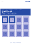
S1C63558
Technical Manual
S1C63558 Technical Hardware
NOTICE
No part of this material may be reproduced or duplicated in any form or by any means without the written permission of Seiko
Epson. Seiko Epson reserves the right to make changes to this material without notice. Seiko Epson does not assume any
liability of any kind arising out of any inaccuracies contained in this material or due to its application or use in any product or
circuit and, further, there is no representation that this material is applicable to products requiring high level reliability, such
as medical products. Moreover, no license to any intellectual property rights is granted by implication or otherwise, and there
is no representation or warranty that anything made in accordance with this material will be free from any patent or copyright
infringement of a third party. This material or portions thereof may contain technology or the subject relating to strategic
products under the control of the Foreign Exchange and Foreign Trade Law of Japan and may require an export license from
the Ministry of International Trade and Industry or other approval from another government agency.
© SEIKO EPSON CORPORATION 2001, All rights reserved.
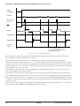
Revisions and Additions for this manual
Chapter
2
Section
2.1.2
Page
8
4
4.7.3
49
S1C63557 Technical Manual
Item
Table 2.1.2.1 LCD drive voltage when
generated internally
Table 4.7.3.1 LCD drive voltage when
generated internally
Contents
The table was revised.
The table was revised.
The information of the product number change
Starting April 1, 2001, the product number has been changed as listed below. Please use the new
product number when you place an order. For further information, please contact Epson sales
representative.
Configuration of product number
Devices
S1
C
63158
F
0A01
00
Packing specification
Specification
Package (D: die form; F: QFP)
Model number
Model name (C: microcomputer, digital products)
Product classification (S1: semiconductor)
Development tools
C
63000
S5U1
A1
1
00
Packing specification
Version (1: Version 1 ∗2)
Tool type (A1: Assembler Package ∗1)
Corresponding model number
(63000: common to S1C63 Family)
Tool classification (C: microcomputer use)
Product classification
(S5U1: development tool for semiconductor products)
∗1: For details about tool types, see the tables below. (In some manuals, tool types are represented by one digit.)
∗2: Actual versions are not written in the manuals.
Comparison table between new and previous number
S1C63 Family processors
S1C63 Family peripheral products
Previous No.
New No.
Previous No.
New No.
E0C63158
E0C63256
E0C63358
E0C63P366
E0C63404
E0C63406
E0C63408
E0C63F408
E0C63454
E0C63455
E0C63458
E0C63466
E0C63P466
S1C63158
S1C63256
S1C63358
S1C6P366
S1C63404
S1C63406
S1C63408
S1C6F408
S1C63454
S1C63455
S1C63458
S1C63466
S1C6P466
E0C63467
E0C63557
E0C63558
E0C63567
E0C63F567
E0C63658
E0C63666
E0C63F666
E0C63A08
E0C63B07
E0C63B08
E0C63B58
S1C63467
S1C63557
S1C63558
S1C63567
S1C6F567
S1C63658
S1C63666
S1C6F666
S1C63A08
S1C63B07
S1C63B08
S1C63B58
Previous No.
E0C5250
E0C5251
New No.
S1C05250
S1C05251
Comparison table between new and previous number of development tools
Development tools for the S1C63 Family
Development tools for the S1C63/88 Family
Previous No.
New No.
Previous No.
New No.
ADP63366
ADP63466
ASM63
GAM63001
ICE63
PRC63001
PRC63002
PRC63004
PRC63005
PRC63006
PRC63007
URS63366
S5U1C63366X
S5U1C63466X
S5U1C63000A
S5U1C63000G
S5U1C63000H1
S5U1C63001P
S5U1C63002P
S5U1C63004P
S5U1C63005P
S5U1C63006P
S5U1C63007P
S5U1C63366Y
ADS00002
GWH00002
URM00002
S5U1C88000X1
S5U1C88000W2
S5U1C88000W1
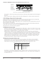
CONTENTS
CONTENTS
CHAPTER
1 OUTLINE ________________________________________________ 1
1.1
1.2
1.3
1.4
1.5
CHAPTER
Features ........................................................................................................ 1
Block Diagram .............................................................................................. 2
Pin Layout Diagram ..................................................................................... 3
Pin Description ............................................................................................. 4
Mask Option .................................................................................................. 5
2 POWER SUPPLY AND INITIAL RESET ____________________________ 8
2.1
Power Supply ................................................................................................ 8
2.1.1 Voltage <VD1> for oscillation circuit and internal circuits ...................... 8
2.1.2 Voltage <VC1–VC5> for LCD driving ........................................................ 8
2.2
Initial Reset ................................................................................................... 9
2.2.1 Reset terminal (RESET) ............................................................................. 9
2.2.2 Simultaneous low input to terminals K00–K03 ........................................ 10
2.2.3 Internal register at initial resetting .......................................................... 10
2.2.4 Terminal settings at initial resetting ......................................................... 11
2.3
CHAPTER
3 CPU, ROM, RAM________________________________________ 12
3.1
3.2
3.3
3.4
CHAPTER
Test Terminal (TEST) ................................................................................... 11
CPU .............................................................................................................. 12
Code ROM ................................................................................................... 12
RAM ............................................................................................................. 12
Data ROM .................................................................................................... 13
4 PERIPHERAL CIRCUITS AND OPERATION __________________________ 14
4.1
4.2
Memory Map ................................................................................................ 14
Watchdog Timer ........................................................................................... 23
4.2.1 Configuration of watchdog timer .............................................................. 23
4.2.2 Interrupt function ...................................................................................... 23
4.2.3 I/O memory of watchdog timer ................................................................. 24
4.2.4 Programming notes ................................................................................... 24
4.3
Oscillation Circuit ....................................................................................... 25
4.3.1 Configuration of oscillation circuit .......................................................... 25
4.3.2 OSC1 oscillation circuit ............................................................................ 25
4.3.3 OSC3 oscillation circuit ............................................................................ 26
4.3.4 Switching the CPU operating clock .......................................................... 26
4.3.5 Clock frequency and instruction execution time ...................................... 26
4.3.6 I/O memory of oscillation circuit .............................................................. 27
4.3.7 Programming notes ................................................................................... 27
4.4
Input Ports (K00–K03 and K10–K13) ......................................................... 28
4.4.1 Configuration of input ports ..................................................................... 28
4.4.2 Interrupt function ...................................................................................... 28
4.4.3 Mask option ............................................................................................... 29
4.4.4 I/O memory of input ports ......................................................................... 30
4.4.5 Programming notes ................................................................................... 32
4.5
Output Ports (R00–R03, R10–R13 and R20–R23) ...................................... 33
4.5.1 Configuration of output ports ................................................................... 33
4.5.2 Mask option ............................................................................................... 33
S1C63558 TECHNICAL MANUAL
EPSON
i
CONTENTS
4.5.3 High impedance control ............................................................................ 34
4.5.4 Special output ............................................................................................ 34
4.5.5 I/O memory of output ports ....................................................................... 37
4.5.6 Programming notes ................................................................................... 40
4.6
I/O Ports (P00–P03, P10–P13, P20–P23 and P30–P33) .......................... 41
4.6.1 Configuration of I/O ports ........................................................................ 41
4.6.2 Mask option ............................................................................................... 42
4.6.3 I/O control registers and input/output mode ............................................ 42
4.6.4 Pull-up during input mode ........................................................................ 42
4.6.5 Special outputs (CL, FR) ........................................................................... 43
4.6.6 I/O memory of I/O ports ............................................................................ 44
4.6.7 Programming notes ................................................................................... 48
4.7
LCD Driver (COM0–COM16, SEG0–SEG39) ........................................... 49
4.7.1 Configuration of LCD driver .................................................................... 49
4.7.2 Mask option ............................................................................................... 49
4.7.3 Power supply for LCD driving .................................................................. 49
4.7.4 LCD display control (ON/OFF) and switching of duty ............................ 49
4.7.5 Display memory ......................................................................................... 51
4.7.6 LCD contrast adjustment .......................................................................... 53
4.7.7 I/O memory of LCD driver ........................................................................ 54
4.7.8 Programming notes ................................................................................... 56
4.8
Clock Timer .................................................................................................. 57
4.8.1 Configuration of clock timer ..................................................................... 57
4.8.2 Data reading and hold function ................................................................ 57
4.8.3 Interrupt function ...................................................................................... 58
4.8.4 I/O memory of clock timer ........................................................................ 59
4.8.5 Programming notes ................................................................................... 60
4.9
Stopwatch Timer .......................................................................................... 61
4.9.1 Configuration of stopwatch timer ............................................................. 61
4.9.2 Count-up pattern ....................................................................................... 61
4.9.3 Interrupt function ...................................................................................... 62
4.9.4 I/O memory of stopwatch timer ................................................................ 63
4.9.5 Programming notes ................................................................................... 64
4.10 Programmable Timer ................................................................................... 65
4.10.1 Configuration of programmable timer ................................................... 65
4.10.2 Setting of initial value and counting down ............................................. 66
4.10.3 Counter mode .......................................................................................... 67
4.10.4 Setting of input clock in timer mode ....................................................... 68
4.10.5 Interrupt function .................................................................................... 69
4.10.6 Setting of TOUT output ........................................................................... 69
4.10.7 Transfer rate setting for serial interface ................................................ 70
4.10.8 I/O memory of programmable timer ....................................................... 71
4.10.9 Programming notes ................................................................................. 76
4.11 Serial Interface ............................................................................................ 77
4.11.1 Configuration of serial interface ............................................................ 77
4.11.2 Mask option ............................................................................................. 78
4.11.3 Transfer modes ........................................................................................ 78
4.11.4 Clock source ............................................................................................ 80
4.11.5 Transmit-receive control ......................................................................... 81
4.11.6 Operation of clock synchronous transfer ................................................ 82
4.11.7 Operation of asynchronous transfer ....................................................... 86
4.11.8 Interrupt function .................................................................................... 90
4.11.9 I/O memory of serial interface ................................................................ 92
4.11.10 Programming notes ............................................................................... 99
4.12 Sound Generator ......................................................................................... 100
4.12.1 Configuration of sound generator ......................................................... 100
4.12.2 Buzzer output circuit .............................................................................. 100
ii
EPSON
S1C63558 TECHNICAL MANUAL
CONTENTS
4.12.3 Control of buzzer output ......................................................................... 101
4.12.4 Setting of buzzer frequency and sound level .......................................... 102
4.12.5 Digital envelope ..................................................................................... 103
4.12.6 One-shot output ...................................................................................... 104
4.12.7 I/O memory of sound generator ............................................................. 105
4.12.8 Programming notes ................................................................................ 108
4.13 SVD (Supply Voltage Detection) Circuit .................................................... 109
4.13.1 Configuration of SVD circuit ................................................................. 109
4.13.2 Mask option ............................................................................................ 109
4.13.3 SVD operation ........................................................................................ 109
4.13.4 I/O memory of SVD circuit ..................................................................... 110
4.13.5 Programming notes ................................................................................ 111
4.14 Telephone Function (Tone/Pulse Dialer) ................................................... 112
4.14.1 Configuration of tone/pulse dialer ........................................................ 112
4.14.2 Mask option ............................................................................................ 113
4.14.3 Operation of telephone function ............................................................ 113
4.14.4 Tone mode (DTMF) ................................................................................ 116
4.14.5 Pulse mode (DP) .................................................................................... 119
4.14.6 Pause ...................................................................................................... 122
4.14.7 Flash ....................................................................................................... 124
4.14.8 Hold-line ................................................................................................. 125
4.14.9 Interrupt .................................................................................................. 126
4.14.10 I/O memory of telephone function ....................................................... 127
4.14.11 Programming notes .............................................................................. 135
4.15 FSK Demodulator ....................................................................................... 136
4.15.1 Configuration of FSK demodulator ....................................................... 136
4.15.2 Mask option ............................................................................................ 138
4.15.3 Ring/carrier detection and interrupt ..................................................... 139
4.15.4 Inputting FSK data ................................................................................. 140
4.15.5 I/O memory of FSK demodulator .......................................................... 142
4.15.6 Programming notes ................................................................................ 144
4.16 Interrupt and HALT .................................................................................... 145
4.16.1 Interrupt factor ....................................................................................... 147
4.16.2 Interrupt mask ........................................................................................ 148
4.16.3 Interrupt vector ...................................................................................... 148
4.16.4 I/O memory of interrupt ......................................................................... 149
4.16.5 Programming notes ................................................................................ 151
CHAPTER
5 SUMMARY OF NOTES ______________________________________ 152
5.1
5.2
5.3
Notes for Low Current Consumption .......................................................... 152
Summary of Notes by Function ................................................................... 153
Precautions on Mounting ........................................................................... 157
CHAPTER
6 BASIC EXTERNAL WIRING DIAGRAM ___________________________ 159
CHAPTER
7 ELECTRICAL CHARACTERISTICS _______________________________ 160
7.1
7.2
7.3
7.4
7.5
7.6
7.7
Absolute Maximum Rating .......................................................................... 160
Recommended Operating Conditions ......................................................... 160
DC Characteristics ..................................................................................... 161
Analog Circuit Characteristics and Power Current Consumption ............ 162
Oscillation Characteristics ......................................................................... 163
Serial Interface (1), (2) AC Characteristics ............................................... 164
FSK Demodulator Characteristics ............................................................. 165
S1C63558 TECHNICAL MANUAL
EPSON
iii
CONTENTS
7.8 Telephone Function Characteristics ........................................................... 166
7.9 Timing Chart ............................................................................................... 166
7.10 Characteristic Curves (reference value) .................................................... 167
CHAPTER
8 PACKAGE _______________________________________________ 169
8.1
8.2
CHAPTER
9 PAD LAYOUT ____________________________________________ 171
9.1
9.2
iv
Plastic Package ........................................................................................... 169
Ceramic Package for Test Samples ............................................................ 170
Diagram of Pad Layout .............................................................................. 171
Pad Coordinates ......................................................................................... 172
EPSON
S1C63558 TECHNICAL MANUAL
CHAPTER 1: OUTLINE
CHAPTER
1 OUTLINE
The S1C63558 is a microcomputer which has a high-performance 4-bit CPU S1C63000 as the core
CPU, ROM (8,192 words × 13 bits), RAM (5,120 words × 4 bits), serial interface, watchdog timer, programmable timer, time base counters (2 systems), SVD circuit, a dot-matrix LCD driver that can drive a
maximum 40 segments × 17 commons, DTMF/DP generator, FSK demodulator and sound generator
built-in. The S1C63558 features high speed operation and low current consumption in an operating
voltage range (2.2 V to 5.5 V), this makes it suitable for applications working with batteries. It is also
suitable for caller ID and portable data bank systems because it has a large capacity of RAM built-in.
1.1 Features
OSC1 oscillation circuit ...................... 32.768 kHz (Typ.) crystal oscillation circuit
OSC3 oscillation circuit ...................... 3.58 MHz (Typ.) ceramic oscillation circuit
Instruction set ..................................... Basic instruction: 46 types (411 instructions with all)
Addressing mode: 8 types
Instruction execution time ................... During operation at 32.768 kHz: 61 µsec 122 µsec 183 µsec
During operation at 3.58 MHz: 0.56 µsec 1.12 µsec 1.68 µsec
ROM capacity ..................................... Code ROM:
8,192 words × 13 bits
Data ROM:
2,048 words × 4 bits (= 8K bits)
RAM capacity ...................................... Data memory:
5,120 words × 4 bits
Display memory: 816 bits (192 words × 4 bits + 48 × 1 bit)
Input port ............................................. 8 bits
(Pull-up resistors may be supplemented ∗1)
Output port .......................................... 12 bits
(It is possible to switch the 8 bits to special output ∗2)
I/O port ................................................ 16 bits
(It is possible to switch the 2 bits to special output and
the 4 bits to serial I/F input/output ∗2)
(8-bit clock synchronous or asynchronous system is selectable)
Serial interface .................................... 2 ch.
LCD driver ........................................... 40 segments × 8, 16 or 17 commons (∗2)/48 segments × 8 commons (∗1)
Time base counter .............................. 2 systems (Clock timer, stopwatch timer)
Programmable timer ........................... Built-in, 2 inputs × 8 bits, with event counter function
Watchdog timer ................................... Built-in
DTMF generator ................................. Built-in
DP generator ...................................... Built-in
FSK demodulator ................................ Built-in (Compatible with ITU-T V.23/Bell 202)
Sound generator ................................. With envelope and 1-shot output functions
Supply voltage detection (SVD) circuit .. 12 values, programmable (2.20 V to 3.30 V)
(It is possible to switch 1 value to the external voltage detection ∗1)
External interrupt ................................ Input port interrupt:
2 systems
Internal interrupt ................................. Clock timer interrupt:
4 systems
Stopwatch timer interrupt:
2 systems
Programmable timer interrupt: 2 systems
Serial interface interrupt:
6 systems
Dialer interrupt:
1 system
FSK interrupt:
2 systems
Power supply voltage ......................... 2.2 V to 5.5 V
Operating temperature range ............. -20°C to 70°C
Current consumption (Typ.) ................ Low-speed operation (OSC1: crystal oscillation):
During HALT (32 kHz)
3.0 V (LCD power OFF)
1.5 µA
3.0 V (LCD power ON)
4 µA
During operation (32 kHz)
3.0 V (LCD power ON)
10 µA
High-speed operation (OSC3: ceramic oscillation):
During operation (3.58 MHz) 3.0 V (LCD power ON)
600 µA
During FSK operation
5.5 V (LCD power ON) 1,800 µA
Package .............................................. QFP15-128pin (plastic) or chip
∗1: Can be selected with mask option ∗2: Can be selected with software
S1C63558 TECHNICAL MANUAL
EPSON
1
CHAPTER 1: OUTLINE
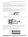
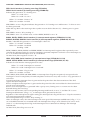
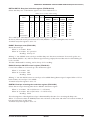
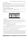
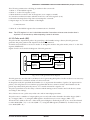
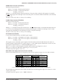
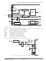
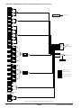
1.2 Block Diagram
ROM
8,192 words × 13 bits
System Reset
Control
RESET
Core CPU S1C63000
OSC1
OSC2
OSC3
OSC4
OSC
Interrupt
Generator
RAM
Stopwatch
Timer
5,120 words × 4 bits
Clock
Timer
Data ROM
2,048 words × 4 bits
COM0–7
SEG0–39
(SEG47–40∗1) COM8–16
Programmable
Timer/Counter
LCD Driver
40 SEG × 17 COM
VDD
VC1–5
CA–CC
VD1
VSS
Input Port
Power
Controller
TEST
Output Port
SVD
TONE
DP
AVDD
AVSS
TIP
RING
FB
BPOUT
CDIN
RDIN
RDRC
VREF
K00–K03
K10–K13
SVD
R00–R03
R10–R13
R20–R23
Sound
Generator
Telephone
Function
I/O Port
FSK
Demodulator
P00–P03
P10–P13
P20–P23
P30–P33
Serial
Interface (1)
Serial
Interface (2)
∗1: Mask option
Fig. 1.2.1 Block diagram
2
EPSON
S1C63558 TECHNICAL MANUAL
CHAPTER 1: OUTLINE
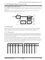
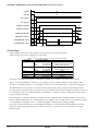
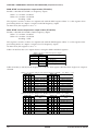
1.3 Pin Layout Diagram
QFP15-128pin
96
65
64
97
S1C63558
INDEX
33
128
1
32
No. Pin name No. Pin name No. Pin name No.
Pin name
1
N.C.
33
SEG4
65
N.C.
97
N.C.
2
SEG34
34
SEG3
66
R10
98
P00
3
SEG33
35
SEG2
67
R03
99
K13
4
SEG32
36
SEG1
68
R02
100
K12
5
SEG31
37
SEG0
69
R01
101
K11
6
SEG30
38
COM7
70
R00
102
K10
7
SEG29
39
COM6
71
CDIN
103
K03
8
SEG28
40
COM5
72
BPOUT 104
K02
9
SEG27
41
COM4
73
RDRC
105
K01
10
SEG26
42
COM3
74
RDIN
106
K00
11
SEG25
43
COM2
75
VREF
107
SVD
12
SEG24
44
COM1
76
AVSS
108
VC1
13
SEG23
45
COM0
77
FB
109
VC23
14
SEG22
46
VSS
78
RING
110
VC4
15
SEG21
47
OSC1
79
TIP
111
VC5
16
SEG20
48
OSC2
80
AVDD
112
CC
17
SEG19
49
VD1
81
P33
113
CB
18
SEG18
50
OSC3
82
P32
114
CA
19
SEG17
51
OSC4
83
P31
115 COM8/SEG47 ∗1
20
SEG16
52
VDD
84
P30
116 COM9/SEG47 ∗1
21
SEG15
53
RESET
85
P23
117 COM10/SEG46 ∗1
22
SEG14
54
TEST
86
P22
118 COM11/SEG45 ∗1
23
SEG13
55
TONE
87
P21
119 COM12/SEG44 ∗1
24
SEG12
56
DP
88
P20
120 COM13/SEG43 ∗1
25
SEG11
57
R23
89
P13
121 COM14/SEG42 ∗1
26
SEG10
58
R22
90
P12
122 COM15/SEG41 ∗1
27
SEG9
59
R21
91
P11
123 COM16/SEG40 ∗1
28
SEG8
60
R20
92
P10
124
SEG39
29
SEG7
61
R13
93
P03
125
SEG38
30
SEG6
62
R12
94
P02
126
SEG37
31
SEG5
63
R11
95
P01
127
SEG36
32
N.C.
64
N.C.
96
N.C.
128
SEG35
∗1: Mask option
N.C. : No Connection
Fig. 1.3.1 Pin layout diagram
S1C63558 TECHNICAL MANUAL
EPSON
3
CHAPTER 1: OUTLINE
1.4 Pin Description
Table 1.4.1 Pin description
Pin name
VDD
VSS
VD1
VC1–VC5
CA–CC
OSC1
OSC2
OSC3
OSC4
K00–K03
K10–K13
P00–P03
P10–P13
P20
P21
P22
P23
P30–P33
R00
R01
R02
R03
R10
R11
R12
R13
R20–R23
COM0–COM7
COM8–COM16
(SEG47–SEG40)
SEG0–SEG39
SVD
DP
TONE
RESET
TEST
AVDD
AVSS
RDIN
TIP
RING
FB
BPOUT
CDIN
RDRC
VREF
4
Pin No.
I/O
52
46
–
–
Power (+) supply pin
Power (–) supply pin
Function
49
–
Oscillation system regulated voltage output pin
108–111
114–112
–
–
LCD system power supply pin (1/4 bias generated internally)
LCD system boosting/reducing capacitor connecting pin
47
I
Crystal oscillation input pin
48
50
O
I
Crystal oscillation output pin
Ceramic oscillation input pin
Ceramic oscillation output pin
51
O
106–103
102–99
98, 95–93
I
I
I/O
Input port
Input port
I/O port
92–89
88
87
I/O
I/O
I/O
I/O port (switching to serial I/F (1) input/output is possible by software)
I/O port
I/O port
86
I/O
I/O port (switching to CL signal output is possible by software)
85
84–81
70
I/O
I/O
O
I/O port (switching to FR signal output is possible by software)
I/O port (switching to serial I/F (2) input/output is possible by software)
Output port (switching to XBZ signal output is possible by software)
69
68
67
O
O
O
Output port (switching to BZ signal output is possible by software)
Output port (switching to TOUT signal output is possible by software)
Output port (switching to FOUT signal output is possible by software)
66
63
62
O
O
O
Output port (switching to XTMUTE signal output is possible by software)
Output port (switching to XRMUTE signal output is possible by software)
Output port (switching to HDO signal output is possible by software)
61
60–57
45–38
O
O
O
Output port (switching to HFO signal output is possible by software)
Output port
LCD common output pin (1/8, 1/16, 1/17 duty can be selected by software)
115–123
O
LCD common output pin
or LCD segment output pin (mask option)
37–33, 31–2, 128–124
107
56
55
53
54
80
76
74
79
78
77
72
71
73
75
O
I
O
O
I
I
–
–
I
I
I
O
O
I
I/O
O
LCD segment output pin
SVD external voltage input pin
Dial pulse output pin
DTMF output pin
Initial reset input pin
Testing input pin
Power (+) supply pin for FSK demodulator
Power (-) supply pin for FSK demodulator
Ring detection input pin
TIP input pin
RING input pin
Input amplifier output pin
Band-pass filter output pin
Carrier detection input pin
I/O pin for connecting RC network
Reference voltage output pin (1/2 VDD)
EPSON
S1C63558 TECHNICAL MANUAL
CHAPTER 1: OUTLINE
1.5 Mask Option
Mask options shown below are provided for the S1C63558. Several hardware specifications are prepared
in each mask option, and one of them can be selected according to the application. The function option
generator FOG63558, that has been prepared as the development software tool of S1C63558, is used for
this selection. Mask pattern of the IC is finally generated based on the data created by the FOG63558.
Refer to the "S5U1C63558D Manual" for the FOG63558.
<Functions selectable with S1C63558 mask options>
(1) External reset by simultaneous LOW input to the input port (K00–K03)
This function resets the IC when several keys are pressed simultaneously. The mask option is used to
select whether this function is used or not. Further when the function is used, a combination of the
input ports (K00–K03), which are connected to the keys to be pressed simultaneously, can be selected.
Refer to Section 2.2.2, "Simultaneous low input to terminals K00–K03", for details.
(2) Time authorize circuit for the simultaneous LOW input reset function
When using the external reset function (shown in 1 above), using the time authorize circuit or not can
be selected by the mask option. The reset function works only when the input time of simultaneous
LOW is more than the rule time if the time authorize circuit is being used.
Refer to Section 2.2.2, "Simultaneous low input to terminals K00–K03", for details.
(3) Input port pull-up resistor
The mask option is used to select whether the pull-up resistor is supplemented to the input ports or
not. It is possible to select for each bit of the input ports.
Refer to Section 4.4.3, "Mask option", for details.
(4) Output specification of the output port
Either complementary output or N-channel open drain output can be selected as the output specification for the output ports. The selection is done in 1-bit units.
Refer to Section 4.5.2, "Mask option", for details.
(5) Output specification / pull-up resistor of the I/O ports
Either complementary output or N-channel open drain output can be selected as the output specification when the I/O ports are in the output mode. The selection is done in 1-bit units.
Further, whether or not the pull-up resistors working in the input mode are supplemented can be
selected. The selection is done in 1-bit units or 4-bit units depending on the I/O port.
1-bit unit: P20, P21, P22, P23
4-bit unit: P00–P03, P10–P13, P30–P33
Refer to Section 4.6.2, "Mask option", for details.
(6) Configuration of the LCD segment
The COM8–COM16 terminals allow selection of terminal specification between COM outputs and
SEG45–SEG40 outputs.
Refer to Section 4.7.2, "Mask option", for details.
(7) External voltage detection of SVD circuit
External voltage (SVD terminal–VSS terminal) detection can be selected in addition to supply voltage
(VDD terminal–VSS terminal) detection. The SVD terminal is used to input the external voltage to be
detected.
Refer to Section 4.13.2, "Mask option", for details.
S1C63558 TECHNICAL MANUAL
EPSON
5
CHAPTER 1: OUTLINE
(8) Output specification of the DP terminal
Either complementary output or N-channel open drain output can be selected as the output specification for the DP (dial pulse output) terminal.
Refer to Section 4.14.2, "Mask option", for details.
(9) Gain of FSK demodulator input amplifier
The gain of the FSK demodulator input amplifier can be either fixed at 1 using the internal feedback
resistor or varied using external resistors.
Refer to Section 4.15.2, "Mask option", for details.
(10)Output specification of other special output terminals
The following special output terminals are shared with the output (R) terminals or the I/O (P)
terminals. Consequently, the output specification (complementary output or N-channel open drain
output) of the shared terminal applies to the special output.
Special output signal
Shared port
XBZ, BZ, TOUT, FOUT
Output ports R00–R03
XRMUTE, XTMUTE, HDO, HFO
Output ports R10–R13
Serial interface input/output
I/O ports P10–P13
CL, FR
I/O ports P22, P23
<Mask option list>
The following is the option list for the S1C63558. Multiple selections are available in each option item as
indicated in the option list. Refer to Chapter 4, "Peripheral Circuits and Operation", to select the specifications that meet the application system. Be sure to select the specifications for unused functions too,
according to the instruction provided. Use fog63558 in the S5U1C63000A package for this selection. Refer
to the "S5U1C63558D Manual" for details.
1. MULTIPLE KEY ENTRY RESET COMBINATION
■
■
■
■
1. Not Use
2. Use <K00, K01, K02, K03>
3. Use <K00, K01, K02>
4. Use <K00, K01>
2. MULTIPLE KEY ENTRY RESET TIME AUTHORIZE
■ 1. Not Use
■ 2. Use
3. INPUT PORT PULL UP RESISTOR
• K00
• K01
• K02
• K03
• K10
• K11
• K12
• K13
■
■
■
■
■
■
■
■
1. With Resistor
1. With Resistor
1. With Resistor
1. With Resistor
1. With Resistor
1. With Resistor
1. With Resistor
1. With Resistor
■
■
■
■
■
■
■
■
2. Gate Direct
2. Gate Direct
2. Gate Direct
2. Gate Direct
2. Gate Direct
2. Gate Direct
2. Gate Direct
2. Gate Direct
4. OUTPUT PORT OUTPUT SPECIFICATION
• R00
• R01
• R02
• R03
• R10
• R11
• R12
• R13
• R20
• R21
• R22
• R23
6
■
■
■
■
■
■
■
■
■
■
■
■
1. Complementary
1. Complementary
1. Complementary
1. Complementary
1. Complementary
1. Complementary
1. Complementary
1. Complementary
1. Complementary
1. Complementary
1. Complementary
1. Complementary
■
■
■
■
■
■
■
■
■
■
■
■
2. Nch-OpenDrain
2. Nch-OpenDrain
2. Nch-OpenDrain
2. Nch-OpenDrain
2. Nch-OpenDrain
2. Nch-OpenDrain
2. Nch-OpenDrain
2. Nch-OpenDrain
2. Nch-OpenDrain
2. Nch-OpenDrain
2. Nch-OpenDrain
2. Nch-OpenDrain
EPSON
S1C63558 TECHNICAL MANUAL
CHAPTER 1: OUTLINE
5. I/O PORT OUTPUT SPECIFICATION
• P00
• P01
• P02
• P03
• P10
• P11
• P12
• P13
• P20
• P21
• P22
• P23
• P30
• P31
• P32
• P33
■
■
■
■
■
■
■
■
■
■
■
■
■
■
■
■
1. Complementary
1. Complementary
1. Complementary
1. Complementary
1. Complementary
1. Complementary
1. Complementary
1. Complementary
1. Complementary
1. Complementary
1. Complementary
1. Complementary
1. Complementary
1. Complementary
1. Complementary
1. Complementary
■
■
■
■
■
■
■
■
■
■
■
■
■
■
■
■
2. Nch-OpenDrain
2. Nch-OpenDrain
2. Nch-OpenDrain
2. Nch-OpenDrain
2. Nch-OpenDrain
2. Nch-OpenDrain
2. Nch-OpenDrain
2. Nch-OpenDrain
2. Nch-OpenDrain
2. Nch-OpenDrain
2. Nch-OpenDrain
2. Nch-OpenDrain
2. Nch-OpenDrain
2. Nch-OpenDrain
2. Nch-OpenDrain
2. Nch-OpenDrain
■
■
■
■
■
■
■
2. Gate Direct
2. Gate Direct
2. Gate Direct
2. Gate Direct
2. Gate Direct
2. Gate Direct
2. Gate Direct
6. I/O PORT PULL UP RESISTOR
• P0x
• P1x
• P20
• P21
• P22
• P23
• P3x
■
■
■
■
■
■
■
1. With Resistor
1. With Resistor
1. With Resistor
1. With Resistor
1. With Resistor
1. With Resistor
1. With Resistor
7. DP PORT OUTPUT SPECIFICATION
■ 1. Complementary
■ 2. Nch-OpenDrain
8. SVD EXTERNAL VOLTAGE DETECTION
■ 1. Not Use
■ 2. Use
9. LCD DRIVER SPECIFICATION
■ 1. 40 seg ∗ 17 com
■ 2. 48 seg ∗ 8 com
10. FSK INTERNAL FEEDBACK RESISTOR
■ 1. Use
■ 2. Not Use
S1C63558 TECHNICAL MANUAL
EPSON
7
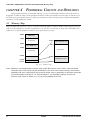
CHAPTER 2: POWER SUPPLY AND INITIAL RESET
CHAPTER 2
POWER SUPPLY AND INITIAL RESET
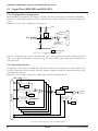
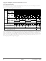
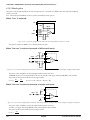
2.1 Power Supply
The S1C63558 operating power voltage is as follows:
Supply voltage VDD = 2.2 V to 5.5 V
The S1C63558 operates by applying a single power supply within the above range between VDD and VSS.
The S1C63558 itself generates the voltage necessary for all the internal circuits by the built-in power
supply circuits shown in Table 2.1.1.
Table 2.1.1 Power supply circuits
Circuit
Power supply circuit
Output voltage
Oscillation and internal circuits
LCD driver
Oscillation system voltage regulator
LCD system voltage circuit
VD1
VC1–VC5
FSK demodulator
Analog system power supply
AVDD, AVDD
Note: • Do not drive external loads with the output voltage from the internal power supply circuits.
• See Chapter 7, "Electrical Characteristics", for voltage values and drive capability.
VDD
AVDD
Internal
circuits
VD1
VD1
External
power
supply
+
-
VC1
VC23
VC4
VC5
CA
CB
CC
Oscillation system
voltage regulator
LCD system
voltage circuit
Oscillation
circuit
VC1 ~ VC5
OSC1~4
LCD driver
COM0~16
SEG0~39
AVSS
VSS
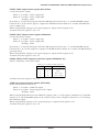
Fig. 2.1.1 Configuration of power supply
2.1.1 Voltage <VD1> for oscillation circuit and internal circuits
VD1 is a voltage for the oscillation circuit and the internal logic circuits, and is generated by the oscillation
system voltage regulator for stabilizing the oscillation. The VD1 voltage is fixed at 2.1 V, so it is not
necessary to control by software.
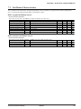
2.1.2 Voltage <VC1–VC5> for LCD driving
VC1, VC23, VC4 and VC5 are the LCD (1/4 bias) drive voltages generated by the LCD system voltage
circuit. These four output voltages can only be supplied to the externally expanded LCD driver.
The LCD system voltage circuit generates VC23 with the voltage regulator built-in, and generates three
other voltages by boosting or reducing the voltage of VC23. Table 2.1.2.1 shows the VC1, VC23, VC4 and VC5
voltage values and boost/reduce status.
Table 2.1.2.1 LCD drive voltage when generated internally
LCD drive voltage
VC1
VC23
VC4
VC5
Boost/reduce status
VC2 × 0.5
VC2 (standard)
VC2 × 1.5
VC2 × 2
Voltage value [V]
1.13
2.25
3.38
4.50
Refer to Section 4.7, "LCD Driver", for control of the LCD drive voltage.
8
EPSON
Note: The LCD drive voltage can
be adjusted by the software
(see Section 4.7.5). Values
in the above table are
typical values.
S1C63558 TECHNICAL MANUAL
CHAPTER 2: POWER SUPPLY AND INITIAL RESET
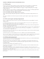
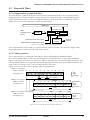
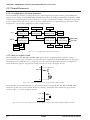
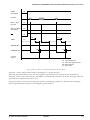
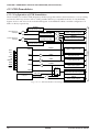
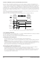
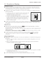
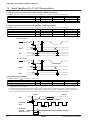
2.2 Initial Reset
To initialize the S1C63558 circuits, initial reset must be executed. There are two ways of doing this.
(1) External initial reset by the RESET terminal
(2) External initial reset by simultaneous low input to terminals K00–K03 (mask option setting)
The circuits are initialized by either (1) or (2). When the power is turned on, be sure to initialize using the
reset function. It is not guaranteed that the circuits are initialized by only turning the power on.
Figure 2.2.1 shows the configuration of the initial reset circuit.
OSC1
OSC2
1 Hz
OSC1
oscillation
circuit
Divider
2 Hz
Mask option
VDD
K00
K01
Mask option
Time
authorize
circuit
K02
Noise
reject
circuit
K03
VDD
R
RESET
Internal
initial
reset
Q
S
Fig. 2.2.1 Configuration of initial reset circuit
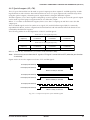
2.2.1 Reset terminal (RESET)
Initial reset can be executed externally by setting the reset terminal to a low level (VSS). After that the
initial reset is released by setting the reset terminal to a high level (VDD) and the CPU starts operating.
The reset input signal is maintained by the RS latch and becomes the internal initial reset signal. The RS
latch is designed to be released by a 2 Hz signal (high) that is divided by the OSC1 clock. Therefore in
normal operation, a maximum of 250 msec (when fOSC1 = 32.768 kHz) is needed until the internal initial
reset is released after the reset terminal goes to high level. Be sure to maintain a reset input of 0.1 msec or
more.
However, when turning the power on, the reset terminal should be set at a low level as in the timing
shown in Figure 2.2.1.1.
2.2 V
VDD
2.0 msec or more
RESET
0.5•VDD
0.1•VDD or less (low level)
Power on
Fig. 2.2.1.1 Initial reset at power on
The reset terminal should be set to 0.1•VDD or less (low level) until the supply voltage becomes 2.2 V or
more. After that, a level of 0.5•VDD or less should be maintained more than 2.0 msec.
S1C63558 TECHNICAL MANUAL
EPSON
9
CHAPTER 2: POWER SUPPLY AND INITIAL RESET
2.2.2 Simultaneous low input to terminals K00–K03
Another way of executing initial reset externally is to input a low signal simultaneously to the input ports
(K00–K03) selected with the mask option.
Since this initial reset passes through the noise reject circuit, maintain the specified input port terminals at
low level for at least 1.5 msec (when the oscillation frequency fOSC1 is 32.768 kHz) during normal operation. The noise reject circuit does not operate immediately after turning the power on until the oscillation
circuit starts oscillating. Therefore, maintain the specified input port terminals at low level for at least 1.5
msec (when the oscillation frequency fOSC1 is 32.768 kHz) after oscillation starts.
Table 2.2.2.1 shows the combinations of input ports (K00–K03) that can be selected with the mask option.
Table 2.2.2.1 Combinations of input ports
1
2
3
Not use
K00∗K01∗K02∗K03
K00∗K01∗K02
4
K00∗K01
When, for instance, mask option 2 (K00∗K01∗K02∗K03) is selected, initial reset is executed when the
signals input to the four ports K00–K03 are all low at the same time. When 3 or 4 is selected, the initial
reset is done when a key entry including a combination of selected input ports is made.
Further, the time authorize circuit can be selected with the mask option. The time authorize circuit checks
the input time of the simultaneous low input and performs initial reset if that time is the defined time (1
to 2 sec) or more.
If using this function, make sure that the specified ports do not go low at the same time during ordinary
operation.
2.2.3 Internal register at initial resetting
Initial reset initializes the CPU as shown in Table 2.2.3.1.
The registers and flags which are not initialized by initial reset should be initialized in the program if
necessary.
In particular, the stack pointers SP1 and SP2 must be set as a pair because all the interrupts including
NMI are masked after initial reset until both the SP1 and SP2 stack pointers are set with software.
When data is written to the EXT register, the E flag is set and the following instruction will be executed in
the extended addressing mode. If an instruction which does not permit extended operation is used as the
following instruction, the operation is not guaranteed. Therefore, do not write data to the EXT register for
initialization only.
Refer to the "S1C63000 Core CPU Manual" for extended addressing and usable instructions.
Table 2.2.3.1 Initial values
Name
Data register A
Data register B
Extension register EXT
Index register X
Index register Y
Program counter
Stack pointer SP1
Stack pointer SP2
Zero flag
Carry flag
Interrupt flag
Extension flag
Queue register
10
CPU core
Symbol Number of bits
A
4
B
4
EXT
8
X
16
Y
16
PC
16
SP1
8
SP2
8
Z
1
C
1
I
1
E
1
Q
16
Setting value
Undefined
Undefined
Undefined
Undefined
Undefined
0110H
Undefined
Undefined
Undefined
Undefined
0
0
Undefined
Name
RAM
Display memory
Other pheripheral circuits
Peripheral circuits
Number of bits
4
4
–
Setting value
Undefined
Undefined
∗
∗ See Section 4.1, "Memory Map".
EPSON
S1C63558 TECHNICAL MANUAL
CHAPTER 2: POWER SUPPLY AND INITIAL RESET
2.2.4 Terminal settings at initial resetting
The output port (R) terminals and I/O port (P) terminals are shared with special output terminals and
input/output terminals of the serial interface. These functions are selected by the software. At initial
reset, these terminals are set to the general purpose output port terminals and I/O port terminals. Set
them according to the system in the initial routine. In addition, take care of the initial status of output
terminals when designing a system.
Table 2.2.4.1 shows the list of the shared terminal settings.
Table 2.2.4.1(a) List of shared terminal settings (Rxx)
Terminal
name
R00
R01
R02
R03
R10
R11
R12
R13
R20–R23
Terminal status
at initial reset
R00 (HIGH output)
R01 (HIGH output)
R02 (HIGH output)
R03 (HIGH output)
R10 (HIGH output)
R11 (HIGH output)
R12 (HIGH output)
R13 (HIGH output)
R20–R23 (HIGH output)
FOUT
TOUT
Special output
BZ XBZ HFO HDO XRMUTE XTMUTE
XBZ
BZ
TOUT
FOUT
XTMUTE
XRMUTE
HDO
HFO
Table 2.2.4.1(b) List of shared terminal settings (Pxx)
Terminal
Terminal status
Special output
Serial I/F *2
CL
FR
Async. Clk-sync. Master Clk-sync. Slave
name
at initial reset
P00–P03 P00–P03 (Input & Pull-up *1)
SIN(I)
SIN(I)
SIN(I)
P10
P10 (Input & Pull-up *1)
SOUT(O)
SOUT(O)
SOUT(O)
P11
P11 (Input & Pull-up *1)
SCLK(O)
SCLK(I)
P12
P12 (Input & Pull-up *1)
SRDY(O)
P13
P13 (Input & Pull-up *1)
P20
P20 (Input & Pull-up *1)
P21
P21 (Input & Pull-up *1)
CL
P22
P22 (Input & Pull-up *1)
FR
P23
P23 (Input & Pull-up *1)
SIN(I)
SIN(I)
SIN(I)
P30
P30 (Input & Pull-up *1)
SOUT(O)
SOUT(O)
SOUT(O)
P31
P31 (Input & Pull-up *1)
SCLK(O)
SCLK(I)
P32
P32 (Input & Pull-up *1)
SRDY(O)
P33
P33 (Input & Pull-up *1)
∗1 When "with pull-up" is selected by mask option (high impedance when "gate direct" is selected)
∗2 The P10–P13 I/O terminals are used for serial I/F (1) and the P30–P33 I/O terminals are for serial I/F (2).
For setting procedure of the functions, see explanations for each of the peripheral circuits.
2.3 Test Terminal (TEST)
This is the terminal used for the factory inspection of the IC. During normal operation, connect the TEST
terminal to VDD.
S1C63558 TECHNICAL MANUAL
EPSON
11
CHAPTER 3: CPU, ROM, RAM
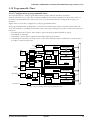
CHAPTER
3 CPU, ROM, RAM
3.1 CPU
The S1C63558 has a 4-bit core CPU S1C63000 built-in as its CPU part.
Refer to the "S1C63000 Core CPU Manual" for the S1C63000.
Note: The SLP instruction cannot be used because the SLEEP operation is not assumed in the S1C63558.
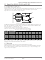
3.2 Code ROM
The built-in code ROM is a mask ROM for loading programs, and has a capacity of 8,192 steps × 13 bits.
The core CPU can linearly access the program space up to step FFFFH from step 0000H, however, the
program area of the S1C63558 is step 0000H to step 1FFFH. The program start address after initial reset is
assigned to step 0110H. The non-maskable interrupt (NMI) vector and hardware interrupt vectors are
allocated to step 0100H and steps 0104H–010EH, respectively.
0000H
0000H
ROM
S1C63558
program area
1FFFH
2000H
0100H
0104H
010EH
S1C63000 core CPU
program space
FFFFH
0110H
Program area
NMI vector
Hardware
interrupt vectors
Program start address
Program area
Unused area
13 bits
Fig. 3.2.1 Configuration of code ROM
3.3 RAM
The RAM is a data memory for storing various kinds of data, and has a capacity of 5,120 words × 4 bits.
The RAM area is assigned to addresses 0000H to 13FFH on the data memory map. Addresses 0100H to
01FFH are 4-bit/16-bit data accessible areas and in other areas it is only possible to access 4-bit data.
When programming, keep the following points in mind.
(1) Part of the RAM area is used as a stack area for subroutine call and register evacuation, so pay
attention not to overlap the data area and stack area.
(2) The S1C63000 core CPU handles the stack using the stack pointer for 4-bit data (SP2) and the stack
pointer for 16-bit data (SP1).
16-bit data are accessed in stack handling by SP1, therefore, this stack area should be allocated to the
area where 4-bit/16-bit access is possible (0100H to 01FFH). The stack pointers SP1 and SP2 change
cyclically within their respective range: the range of SP1 is 0000H to 03FFH and the range of SP2 is
0000H to 00FFH. Therefore, pay attention to the SP1 value because it may be set to 0200H or more
exceeding the 4-bit/16-bit accessible range in the S1C63558 or it may be set to 00FFH or less. Memory
accesses except for stack operations by SP1 are 4-bit data access.
After initial reset, all the interrupts including NMI are masked until both the stack pointers SP1 and
SP2 are set by software. Further, if either SP1 or SP2 is re-set when both are set already, the interrupts
including NMI are masked again until the other is re-set. Therefore, the settings of SP1 and SP2 must
be done as a pair.
12
EPSON
S1C63558 TECHNICAL MANUAL
CHAPTER 3: CPU, ROM, RAM
(3) Subroutine calls use 4 words (for PC evacuation) in the stack area for 16-bit data (SP1). Interrupts use
4 words (for PC evacuation) in the stack area for 16-bit data (SP1) and 1 word (for F register evacuation) in the stack area for 4-bit data.
0000H
4-bit access area
(SP2 stack area)
00FFH
0100H
4/16-bit access area
(SP1 stack area)
01FFH
0200H
4-bit access area
(Data area)
13FFH
4 bits
Fig. 3.3.1 Configuration of data RAM
3.4 Data ROM
The data ROM is a mask ROM for loading various static data such as a character generator, and has a
capacity of 2,048 words × 4 bits. The data ROM is assigned to addresses 8000H to 87FFH on the data
memory map, and the data can be read using the same data memory access instructions as the RAM.
S1C63558 TECHNICAL MANUAL
EPSON
13
CHAPTER 4: PERIPHERAL CIRCUITS AND OPERATION (Memory Map)
CHAPTER
4 PERIPHERAL CIRCUITS AND OPERATION
The peripheral circuits of S1C63558 (timer, I/O, etc.) are interfaced with the CPU in the memory
mapped I/O method. Thus, all the peripheral circuits can be controlled by accessing the I/O memory on
the memory map using the memory operation instructions. The following sections explain the detailed
operation of each peripheral circuit.
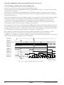
4.1 Memory Map
The S1C63558 data memory consists of 5,120-word RAM, 2,048-word data ROM, 816-bit display memory
and 97-word peripheral I/O memory. Figure 4.1.1 shows the overall memory map of the S1C63558, and
Tables 4.1.1(a)–(h) the peripheral circuits' (I/O space) memory maps.
0000H
RAM area
1400H
F000H
Unused area
Display memory area
8000H
F25EH
Data ROM area
8800H
Unused area
Unused area
F000H
FF00H
FFFFH
FF00H
Peripheral I/O area
I/O memory area
FFFFH
Fig. 4.1.1 Memory map
Note: Memory is not implemented in unused areas within the memory map. Further, some non-implementation areas and unused (access prohibition) areas exist in the display memory area and the
peripheral I/O area. If the program that accesses these areas is generated, its operation cannot be
guaranteed. Refer to Section 4.7.5, "Display memory", for the display memory, and the I/O
memory maps shown in Tables 4.1.1 (a)–(h) for the peripheral I/O area.
14
EPSON
S1C63558 TECHNICAL MANUAL
CHAPTER 4: PERIPHERAL CIRCUITS AND OPERATION (Memory Map)
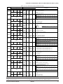
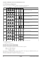
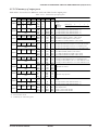
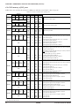
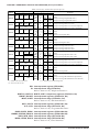
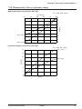
Table 4.1.1 (a) I/O memory map (FF00H–FF18H)
Address
Register
D3
D2
D1
D0
CLKCHG OSCC
0
Dummy
R/W
R
R/W
FF00H
SVDS3 SVDS2 SVDS1 SVDS0
FF04H
R/W
0
0
SVDDT SVDON
FF05H
R
R/W
FOUTE
0
FOFQ1 FOFQ0
R/W
R
R/W
0
0
WDEN WDRST
FF06H
FF07H
R
TPS
0
R/W
R
PTS3
PTS2
R/W
W
MB
DRS
FF10H
R/W
PTS1
PTS0
FF11H
R/W
FTS3
FTS2
FTS1
FTS0
FF12H
R/W
CHFO
CHDO
CRMO
CTMO
FF13H
R/W
HF
HOLD
PAUSE FLASH
FF14H
R/W
IDP3
W
IDP2
IDP1
IDP0
SINR
SINC
FF15H
R/W
CTO
0
R/W
R
TCD3
TCD2
FF16H
R/W
TCD1
TCD0
FF17H
R/W
HSON
0
CRMUT CTMUT
R/W
R
R/W
FF18H
Comment
Name Init ∗1
1
0
CLKCHG
0
OSC3 OSC1 CPU clock switch
OSCC
0
On
Off
OSC3 oscillation On/Off
0 ∗3
– ∗2
Unused
Dummy
0
General-purpose register
SVD criteria voltage setting
SVDS3
0
1
2
3
4
5
6
7
[SVDS3–0] 0
SVDS2
0
Voltage(V) 2.20/1.05 2.20 2.20 2.20 2.20 2.30 2.40 2.50
SVDS1
0
[SVDS3–0] 8
9
10
11
12
13
14
15
SVDS0
0
Voltage(V) 2.60 2.70 2.80 2.90 3.00 3.10 3.20 3.30
Unused
– ∗2
0 ∗3
0 ∗3
– ∗2
Unused
SVDDT
0
Low Normal SVD evaluation data
SVDON
0
On
Off
SVD circuit On/Off
R03 output selection (R03 should be fixed at "1".)
FOUTE
0
FOUT
DC
Unused
0 ∗3
– ∗2
FOUT
FOFQ1
0
1
2
[FOFQ1, 0]
0
3
frequency
Frequency fOSC1/64 fOSC1/8 fOSC1 fOSC3
FOFQ0
0
selection
0 ∗3
– ∗2
Unused
0 ∗3
– ∗2
Unused
WDEN
1
Enable Disable Watchdog timer enable
WDRST∗3 Reset Reset Invalid Watchdog timer reset (writing)
TPS
0
Pulse
Tone Tone / pulse mode selection
0 ∗3
Unused
– ∗2
MB
0
33.3:66.6 40:60 Make : Break ratio selection
DRS
0
20pps 10pps Dialing pulse rate selection
Pause time selection (initial value: 4 sec)
PTS3
0
1
2
3
4
5
6
7
[PTS3–0] 0
PTS2
1
1
2
3
4
5
6
7
Time(sec) ×
PTS1
0
9
10
11
12
13
14
15
[PTS3–0] 8
PTS0
0
9
10
11
12
13
14
15
Time(sec) 8
Flash time selection (initial value: 563 ms)
FTS3
0
1
2
3
4
5
6
7
[FTS3–0] 0
FTS2
1
94 188 281 375 469 563 656
Time(ms) ×
FTS1
1
9
10
11
12
13
14
15
[FTS3–0] 8
FTS0
0
Time(ms) 750 844 938 1031 1125 1219 1313 1406
CHFO
DC
R13 output selection (R13 should be fixed at "1".)
0
HFO
CHDO
DC
R12 output selection (R12 should be fixed at "1".)
0
HDO
XRMUTE DC
CRMO
R11 output selection (R11 should be fixed at "1".)
0
XTMUTE DC
CTMO
R10 output selection (R10 should be fixed at "1".)
0
HF
0
Hand free
Yes
No
HOLD
0
Hold-line function
On
Off
PAUSE∗3
0
Pause function
Yes
No
FLASH∗3
0
Flash function
Yes
No
Inter-digit pause selection for dial pulse (initial value: 750 ms)
IDP3
1
1
2
3
4
5
6
7
[IDP3–0] 0
IDP2
0
94 188 281 375 469 563 656
Time(ms) ×
IDP1
0
9
10
11
12
13
14
15
[IDP3–0] 8
IDP0
0
Time(ms) 750 844 938 1031 1125 1219 1313 1406
CTO
Continuous tone output On/Off
0
On
Off
0 ∗3
Unused
– ∗2
SINR
1
Enable Disable DTMF row frequency output enable
Enable Disable DTMF column frequency output enable
SINC
1
TCD3
Telephone code for dialing
0
[TCD3–0] 0
1
2
3
4
5
6
7
TCD2
0
DTMF (R1C4) (R1C1) (R1C2) (R1C3) (R2C1) (R2C2) (R2C3) (R3C1)
×
1
2
3
4
5
6
7
DP
TCD1
0
9
10
11
12
13
14
15
[TCD3–0] 8
DTMF (R3C2) (R3C3) (R4C2) (R4C3) (R4C1) (R2C4) (R4C4) (R3C4)
TCD0
0
8
9
10
11
12
13
14
15
DP
HSON
0 ∗3
CRMUT
CTMUT
0
– ∗2
1
1
Off
On
Mute
Mute
0
0
Hook switch On/Off
Unused
Receive mute control
Transmit mute control
Remarks
∗1 Initial value at initial reset
∗2 Not set in the circuit
S1C63558 TECHNICAL MANUAL
∗3 Constantly "0" when being read
∗4 Depends on the input status of the RDIN terminal
EPSON
15
CHAPTER 4: PERIPHERAL CIRCUITS AND OPERATION (Memory Map)
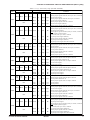
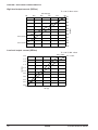
Table 4.1.1 (b) I/O memory map (FF20H–FF42H)
Address
Register
D3
D2
D1
D0
SIK03
SIK02
SIK01
SIK00
FF20H
R/W
K03
K02
K01
K00
FF21H
R
KCP03 KCP02 KCP01 KCP00
FF22H
R/W
SIK13
SIK12
SIK11
SIK10
FF24H
R/W
FF25H
K13
(EVIN)
K12
K11
K10
R
KCP13 KCP12 KCP11 KCP10
FF26H
R/W
R03HIZ R02HIZ R01HIZ R00HIZ
FF30H
R/W
FF31H
R03
R02
(FOUT) (TOUT)
R01
(BZ)
R00
(XBZ)
R/W
R13HIZ R12HIZ R11HIZ R10HIZ
FF32H
R/W
FF33H
R13
(HFO)
R12
R11
R10
(HDO) (XRMUTE) (XTMUTE)
R/W
R23HIZ R22HIZ R21HIZ R20HIZ
FF34H
R/W
R23
R22
R21
R20
IOC01
IOC00
FF35H
R/W
IOC03
IOC02
FF40H
R/W
PUL03
PUL02
PUL01
PUL00
FF41H
R/W
P03
P02
P01
FF42H
R/W
16
P00
Comment
Name Init ∗1
1
0
SIK03
0
Enable Disable
SIK02
0
Enable Disable
K00–K03 interrupt selection register
SIK01
0
Enable Disable
SIK00
0
Enable Disable
K03
– ∗2 High
Low
– ∗2 High
K02
Low
K00–K03 input port data
– ∗2 High
K01
Low
∗2
–
K00
High
Low
KCP03
1
KCP02
1
K00–K03 input comparison register
KCP01
1
KCP00
1
SIK13
0
Enable Disable
SIK12
0
Enable Disable
K10–K13 interrupt selection register
SIK11
0
Enable Disable
SIK10
0
Enable Disable
K13
– ∗2 High
Low
– ∗2 High
K12
Low
K10–K13 input port data
– ∗2 High
K11
Low
∗2
–
K10
High
Low
KCP13
1
KCP12
1
K10–K13 input comparison register
KCP11
1
KCP10
1
R03HIZ
0
Hi-Z
Output R03 (FOUTE=0)/FOUT (FOUTE=1) Hi-z control
R02HIZ
0
Hi-Z
Output R02 (PTOUT=0)/TOUT (PTOUT=1) Hi-z control
R01HIZ
0
Hi-Z
Output R01 (BZOUT=0)/BZ (BZOUT=1) Hi-z control
R00HIZ
0
Hi-Z
Output R00 (XBZOUT=0)/XBZ (XBZOUT=1) Hi-z control
R03
1
High
Low R03 output port data (FOUTE=0) Fix at "1" when FOUT is used.
R02
1
High
Low R02 output port data (PTOUT=0) Fix at "1" when TOUT is used.
R01
1
High
Low R01 output port data (BZOUT=0) Fix at "1" when BZ is used.
R00
1
High
Low R00 output port data (XBZOUT=0) Fix at "1" when XBZ is used.
R13HIZ
0
Hi-Z
Output R13 (CHFO=0)/HFO (CHFO=1) Hi-z control
R12HIZ
0
Hi-Z
Output R12 (CHDO=0)/HDO (CHDO=1) Hi-z control
R11HIZ
0
Hi-Z
Output R11 (CRMO=0)/XRMUTE (CRMO=1) Hi-z control
R10HIZ
0
Hi-Z
Output R10 (CTMO=0)/XTMUTE (CTMO=1) Hi-z control
R13
1
High
Low R13 output port data (CHFO=0) Fix at "1" when HFO is used.
R12
1
High
Low R12 output port data (CHDO=0) Fix at "1" when HDO is used.
R11
1
High
Low R11 output port data (CRMO=0) Fix at "1" when XRMUTE is used.
R10
1
High
Low R10 output port data (CTMO=0) Fix at "1" when XTMUTE is used.
R23HIZ
0
Hi-Z
Output
R22HIZ
0
Hi-Z
Output
R20–R23 Hi-z control
R21HIZ
0
Hi-Z
Output
R20HIZ
0
Hi-Z
Output
R23
1
High
Low
R22
1
High
Low
R20–R23 output port data
R21
1
High
Low
R20
1
High
Low
IOC03
0
Output Input
IOC02
0
Output Input
P00–P03 I/O control register
IOC01
0
Output Input
IOC00
0
Output Input
PUL03
1
On
Off
PUL02
1
On
Off
P00–P03 pull-up control register
PUL01
1
On
Off
PUL00
1
On
Off
P03
– ∗2 High
Low
– ∗2 High
P02
Low
P00–P03 I/O port data
– ∗2 High
P01
Low
∗2
–
P00
High
Low
EPSON
S1C63558 TECHNICAL MANUAL
CHAPTER 4: PERIPHERAL CIRCUITS AND OPERATION (Memory Map)
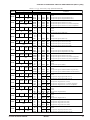
Table 4.1.1 (c) I/O memory map (FF44H–FF4DH)
Address
Register
D3
IOC13
D2
D1
IOC12
IOC11
D0
IOC10
FF44H
R/W
PUL13
PUL12
PUL11
PUL10
Name
IOC13
Init ∗1
0
1
Output
0
Input
IOC12
0
Output
Input
IOC11
0
Output
Input
IOC10
0
Output
Input
PUL13
1
On
Off
PUL12
1
On
Off
PUL11
1
On
Off
PUL10
1
On
Off
P13
– ∗2
High
Low
P12
– ∗2
High
Low
P11
– ∗2
High
Low
P10
– ∗2
High
Low
FF45H
R/W
P13
P12
P11
(XSRDY) (XSCLK) (SOUT)
P10
(SIN)
FF46H
R/W
IOC23
IOC22
IOC21
FF48H
R/W
PUL23
PUL22
PUL21
R/W
P22
(CL)
P21
R/W
IOC32
IOC31
IOC30
FF4CH
R/W
PUL33
PUL32
PUL31
Output
Input
IOC22
0
Output
Input
IOC21
IOC20
PUL23
0
0
1
Output
Output
On
Input
Input
Off
PUL22
1
On
Off
PUL21
PUL20
P23
1
1
– ∗2
On
On
High
Off
Off
Low
P22
– ∗2
High
Low
P21
P20
IOC33
– ∗2
– ∗2
0
High
High
Output
Low
Low
Input
IOC32
0
Output
Input
IOC31
0
Output
Input
IOC30
0
Output
Input
PUL33
1
On
Off
PUL32
1
On
Off
PUL31
1
On
Off
PUL30
1
On
Off
P20
FF4AH
IOC33
0
PUL20
FF49H
P23
(FR)
IOC23
IOC20
PUL30
FF4DH
R/W
S1C63558 TECHNICAL MANUAL
EPSON
Comment
P13 I/O control register
General-purpose register when SIF (clock sync. slave) is selected
P12 I/O control register
General-purpose register when SIF (clock sync.) is selected
P11 I/O control register (ESIF=0)
General-purpose register when SIF is selected
P10 I/O control register (ESIF=0)
General-purpose register when SIF is selected
P13 pull-up control register
General-purpose register when SIF (clock sync. slave) is selected
P12 pull-up control register
General-purpose register when SIF (clock sync. master) is selected
SCLK (I) pull-up control register
when SIF (clock sync. slave) is selected
P11 pull-up control register (ESIF=0)
General-purpose register when SIF is selected
P10 pull-up control register (ESIF=0)
SIN pull-up control register when SIF is selected
P13 I/O port data
General-purpose register when SIF (clock sync. slave) is selected
P12 I/O port data
General-purpose register when SIF (clock sync.) is selected
P11 I/O port data (ESIF=0)
General-purpose register when SIF is selected
P10 I/O port data (ESIF=0)
General-purpose register when SIF is selected
P23 I/O control register (EXLCDC=0)
General-purpose register when FR output is selected
P22 I/O control register (EXLCDC=0)
General-purpose register when CL output is selected
P21 I/O control register
P20 I/O control register
P23 pull-up control register (EXLCDC=0)
General-purpose register when FR output is selected
P22 pull-up control register (EXLCDC=0)
General-purpose register when CL output is selected
P21 pull-up control register
P20 pull-up control register
P23 I/O port data (EXLCDC=0)
General-purpose register when FR output is selected
P22 I/O port data (EXLCDC=0)
General-purpose register when CL output is selected
P21 I/O port data
P20 I/O port data
P33 I/O control register
General-purpose register when SIF (clock sync. slave) is selected
P32 I/O control register
General-purpose register when SIF (clock sync.) is selected
P31 I/O control register (ESIFS=0)
General-purpose register when SIF is selected
P30 I/O control register (ESIFS=0)
General-purpose register when SIF is selected
P33 pull-up control register
General-purpose register when SIF (clock sync. slave) is selected
P32 pull-up control register
General-purpose register when SIF (clock sync. master) is selected
SCLK (I) pull-up control register
when SIF (clock sync. slave) is selected
P31 pull-up control register (ESIFS=0)
General-purpose register when SIF is selected
P30 pull-up control register (ESIFS=0)
SIN pull-up control register when SIF is selected
17
CHAPTER 4: PERIPHERAL CIRCUITS AND OPERATION (Memory Map)
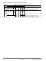
Table 4.1.1 (d) I/O memory map (FF4EH–FF67H)
Address
Register
D3
D2
D1
D0
P33
P32
P31
P30
(XSRDYS) (XSCLKS) (SOUTS) (SINS)
FF4EH
R/W
Name
P33
P32
– ∗2
P31
– ∗2
P30
– ∗2
0 ∗3
SMD1S
FF58H
SMD0S
R
R/W
ESIFS
EPRS
EPRS PMDS SCS1S SCS0S
PMDS
FF59H
SCS1S
R/W
SCS0S
RXTRGS
RXTRGS RXENS TXTRGS TXENS
RXENS
FF5AH
TXTRGS
R/W
TXENS
0 ∗3
0
FERS PERS OERS FERS
– ∗2
0
0
0
0
0
0
0
0
FF5BH
PERS
0
OERS
0
SMD1S SMD0S ESIFS
0
R
R/W
TRXD3S
TRXD2S
FF5CH
TRXD1S
R/W
TRXD0S
TRXD7S
TRXD7S TRXD6S TRXD5S TRXD4S
TRXD6S
FF5DH
TRXD5S
R/W
TRXD4S
LDUTY1
LDUTY1 LDUTY0 Dummy LPWR
LDUTY0
FF60H
Dummy
R/W
LPWR
EXLCDC
EXLCDC ALOFF ALON LPAGE ALOFF
FF61H
ALON
LPAGE
R/W
TRXD3S TRXD2S TRXD1S TRXD0S
LC3
LC3
LC2
LC1
R/W
LC0
0 ∗3
0
BZOUT XBZOUT
0 ∗3
BZOUT
R/W
XBZOUT
FSKON
0
RDET CDET
0 ∗3
RDET
R
CDET
0 ∗3
0
RDETCP CDETCP
0 ∗3
RDETCP
R/W
CDETCP
LC2
FF62H
0
FF65H
R
FSKON
FF66H
R/W
0
FF67H
R
18
Init ∗1
– ∗2
LC1
LC0
0
0
0
– ∗2
0
1
High
0
Low
Comment
P33 I/O port data
General-purpose register when SIF (clock sync. slave) is selected
Low P32 I/O port data
High
General-purpose register when SIF (clock sync.) is selected
Low P31 I/O port data (ESIFS=0)
High
General-purpose register when SIF is selected
Low P30 I/O port data (ESIFS=0)
High
General-purpose register when SIF is selected
0
1
[SMD1S, 0S]
Unused
Clk-sync. master Clk-sync. slave
Mode
Serial I/F (2)
2
3
[SMD1S, 0S]
mode selection Mode
Async. 7-bit
Async. 8-bit
SIF
I/O
Serial I/F (2) enable (P3x port function selection)
Enable Disable Serial I/F (2) parity enable register
Odd
Even Serial I/F (2) parity mode selection
SIF (2) clock
[SCS1S, 0S] 0
1
2
3
1200bps 600bps 2400bps PT
source selection Mode
Run
Stop Serial I/F (2) receive status (reading)
Trigger
–
Serial I/F (2) receive trigger (writing)
Enable Disable Serial I/F (2) receive enable
Run
Stop Serial I/F (2) transmit status (reading)
Trigger
–
Serial I/F (2) transmit trigger (writing)
Enable Disable Serial I/F (2) transmit enable
Unused
Error No error Serial I/F (2) framing error flag status (reading)
Reset
–
Serial I/F (2) framing error flag reset (writing)
Error No error Serial I/F (2) parity error flag status (reading)
Reset
–
Serial I/F (2) parity error flag reset (writing)
Error No error Serial I/F (2) overrun error flag status (reading)
Reset
–
Serial I/F (2) overrun error flag reset (writing)
High
Low
High
Low
Serial I/F (2) transmit/receive data (low-order 4 bits)
High
Low
LSB
High
Low
High
MSB
Low
High
Low
Serial I/F (2) transmit/receive data (high-order 4 bits)
High
Low
High
Low
LCD drive duty
[LDUTY1, 0]
0
1
2, 3
Duty
1/17
1/16
1/8
switch
General-purpose register
LCD power On/Off
On
Off
– ∗2
– ∗2
– ∗2
– ∗2
– ∗2
– ∗2
– ∗2
– ∗2
0
0
0
0
0
Enable Disable Expanded LCD driver signal control
1
All Off Normal LCD all Off control
0
All On Normal LCD all On control
F100-F15F F000-F05F Display memory area selection (when 1/8 duty is selected)
0
General-purpose register when 1/16, 1/17 duty is selected
LCD contrast adjustment
– ∗2
– ∗2
[LC3–0]
0
–
15
Contrast
Light
–
Dark
– ∗2
– ∗2
– ∗2
– ∗2
0
0
0
– ∗2
– ∗4
0
– ∗2
– ∗2
0
0
BZ
XBZ
On
Ring
Carrier
Unused
Unused
DC
R01 output selection (R01 should be fixed at "1".)
DC
R00 output selection (R00 should be fixed at "1".)
Off
FSK demodulator On/Off
Unused
No Ring Ring detection bit
No Carrier Carrier detection bit
Unused
Unused
RDET comparison register
CDET comparison register
EPSON
S1C63558 TECHNICAL MANUAL
CHAPTER 4: PERIPHERAL CIRCUITS AND OPERATION (Memory Map)
Table 4.1.1 (e) I/O memory map (FF6CH–FF7AH)
Address
FF6CH
FF6DH
FF6EH
FF6FH
FF70H
FF71H
FF72H
FF73H
FF74H
FF75H
FF76H
FF78H
FF79H
FF7AH
Register
Name Init ∗1
1
ENRTM
0
1sec
ENRTM ENRST ENON
BZE
ENRST∗3 Reset Reset
ENON
0
On
R/W
W
R/W
BZE
0
Enable
0 ∗3
– ∗2
0
BZSTP BZSHT SHTPW BZSTP∗3
0
Stop
BZSHT
0
Trigger
Busy
R
W
R/W
SHTPW
0
125msec
– ∗2
0 ∗3
0
BZFQ2 BZFQ1 BZFQ0
BZFQ2
0
BZFQ1
0
R
R/W
BZFQ0
0
0 ∗3
– ∗2
0
BDTY2 BDTY1 BDTY0
BDTY2
0
BDTY1
0
R
R/W
BDTY0
0
0 ∗3
– ∗2
0
SMD1 SMD0
ESIF
SMD1
0
SMD0
0
R
R/W
ESIF
0
SIF
EPR
0
Enable
EPR
PMD
SCS1 SCS0
PMD
0
Odd
SCS1
0
R/W
SCS0
0
Run
0
RXTRG
Trigger
RXTRG RXEN TXTRG TXEN
0
Enable
RXEN
0
Run
TXTRG
Trigger
R/W
0
TXEN
Enable
– ∗2
0 ∗3
Error
FER
0
0
FER
PER
OER
Reset
PER
0
Error
Reset
R
R/W
OER
0
Error
Reset
TRXD3
– ∗2 High
TRXD3 TRXD2 TRXD1 TRXD0
– ∗2 High
TRXD2
– ∗2 High
TRXD1
R/W
– ∗2 High
TRXD0
TRXD7
– ∗2 High
TRXD7 TRXD6 TRXD5 TRXD4
– ∗2 High
TRXD6
– ∗2 High
TRXD5
R/W
– ∗2 High
TRXD4
0 ∗3
– ∗2
0
0
0
SIFTM
0 ∗3
– ∗2
0 ∗3
– ∗2
R
R/W
SIFTM
0
0 ∗3
– ∗2
0
0
TMRST TMRUN
0 ∗3
– ∗2
TMRST∗3 Reset Reset
R
W
R/W
TMRUN
0
Run
TM3
0
TM3
TM2
TM1
TM0
TM2
0
TM1
0
R
TM0
0
TM7
0
TM7
TM6
TM5
TM4
TM6
0
TM5
0
R
TM4
0
D3
D2
D1
S1C63558 TECHNICAL MANUAL
D0
0
0.5sec
Invalid
Off
Disable
Invalid
Invalid
Ready
31.25msec
Comment
Envelope releasing time selection
Envelope reset (writing)
Envelope On/Off
Buzzer output enable
Unused
1-shot buzzer stop (writing)
1-shot buzzer trigger (writing)
1-shot buzzer status (reading)
1-shot buzzer pulse width setting
Unused
[BZFQ2, 1, 0]
0
1
2
3
Buzzer
Frequency (Hz) 4096.0 3276.8 2730.7 2340.6
frequency
[BZFQ2, 1, 0]
4
5
6
7
Frequency (Hz) 2048.0 1638.4 1365.3 1170.3
selection
Unused
Buzzer signal duty ratio selection
(refer to main manual)
0
1
[SMD1, 0]
Unused
Clk-sync. master Clk-sync. slave
Mode
Serial I/F (1)
2
3
[SMD1, 0]
mode selection Mode
Async. 7-bit
Async. 8-bit
I/O
Serial I/F (1) enable (P1x port function selection)
Disable Serial I/F (1) parity enable register
Even Serial I/F (1) parity mode selection
SIF (1) clock
[SCS1, 0]
0
1
2
3
1200bps 600bps 2400bps PT
source selection Mode
Stop
–
Disable
Stop
–
Disable
Serial I/F (1) receive status (reading)
Serial I/F (1) receive trigger (writing)
Serial I/F (1) receive enable
Serial I/F (1) transmit status (reading)
Serial I/F (1) transmit trigger (writing)
Serial I/F (1) transmit enable
Unused
No error Serial I/F (1) framing error flag status (reading)
–
Serial I/F (1) framing error flag reset (writing)
No error Serial I/F (1) parity error flag status (reading)
–
Serial I/F (1) parity error flag reset (writing)
No error Serial I/F (1) overrun error flag status (reading)
–
Serial I/F (1) overrun error flag reset (writing)
Low
Low
Serial I/F (1) transmit/receive data (low-order 4 bits)
Low
LSB
Low
MSB
Low
Low
Serial I/F (1) transmit/receive data (high-order 4 bits)
Low
Low
Unused
Unused
Unused
Serial I/F test mode (disabled. Do not change.)
Unused
Unused
Invalid Clock timer reset (writing)
Stop Clock timer Run/Stop
Clock timer data (16 Hz)
Clock timer data (32 Hz)
Clock timer data (64 Hz)
Clock timer data (128 Hz)
Clock timer data (1 Hz)
Clock timer data (2 Hz)
Clock timer data (4 Hz)
Clock timer data (8 Hz)
EPSON
19
CHAPTER 4: PERIPHERAL CIRCUITS AND OPERATION (Memory Map)
Table 4.1.1 (f) I/O memory map (FF7CH–FFCBH)
Address
Register
D3
D2
D1
0
0
SWRST
FF7CH
R
SWD3
W
SWD2
SWD1
FF7DH
R
SWD7
SWD6
SWD5
FF7EH
R
0
EVCNT FCSEL
FFC0H
R
R/W
CHSEL PTOUT CKSEL1
FFC1H
R/W
PTPS01 PTPS00 PTRST0
FFC2H
R/W
W
PTPS11 PTPS10 PTRST1
FFC3H
R/W
RLD03
W
RLD02
RLD01
FFC4H
R/W
RLD07
RLD06
RLD05
FFC5H
R/W
RLD13
RLD12
RLD11
FFC6H
R/W
RLD17
RLD16
RLD15
FFC7H
R/W
PTD03
PTD02
PTD01
FFC8H
R
PTD07
PTD06
PTD05
FFC9H
R
PTD13
PTD12
PTD11
FFCAH
R
PTD17
PTD16
PTD15
FFCBH
R
20
Name Init ∗1
1
0 ∗3
– ∗2
SWRUN
0 ∗3
– ∗2
SWRST∗3 Reset Reset
R/W
SWRUN
0
Run
SWD3
0
SWD0
SWD2
0
SWD1
0
SWD0
0
SWD7
0
SWD4
SWD6
0
SWD5
0
SWD4
0
0 ∗3
– ∗2
PLPOL
EVCNT
0
Event ct.
FCSEL
0
With NR
PLPOL
0
CHSEL
0
Timer1
CKSEL0
PTOUT
0
On
CKSEL1
0
OSC3
CKSEL0
0
OSC3
PTPS01
0
PTRUN0
PTPS00
0
PTRST0∗3
– ∗2 Reset
R/W
PTRUN0
0
Run
PTPS11
0
PTRUN1
PTPS10
0
PTRST1∗3
– ∗2 Reset
R/W
PTRUN1
0
Run
RLD03
0
RLD00
RLD02
0
RLD01
0
RLD00
0
RLD07
0
RLD04
RLD06
0
RLD05
0
RLD04
0
RLD13
0
RLD10
RLD12
0
RLD11
0
RLD10
0
RLD17
0
RLD14
RLD16
0
RLD15
0
RLD14
0
PTD03
0
PTD00
PTD02
0
PTD01
0
PTD00
0
PTD07
0
PTD04
PTD06
0
PTD05
0
PTD04
0
PTD13
0
PTD10
PTD12
0
PTD11
0
PTD10
0
PTD17
0
PTD14
PTD16
0
PTD15
0
PTD14
0
D0
Comment
0
Unused
Unused
Invalid Stopwatch timer reset (writing)
Stop Stopwatch timer Run/Stop
Stopwatch timer data
BCD (1/100 sec)
Stopwatch timer data
BCD (1/10 sec)
Unused
Timer Timer 0 counter mode selection
No NR Timer 0 function selection (for event counter mode)
Timer 0 pulse polarity selection (for event counter mode)
Timer0 TOUT output channel selection
TOUT output control
Off
OSC1 Prescaler 1 source clock selection
OSC1 Prescaler 0 source clock selection
[PTPS01, 00]
0
1
2
3
Prescaler 0
division ratio
Division ratio 1/1 1/4 1/32 1/256
selection
Invalid Timer 0 reset (reload)
Stop Timer 0 Run/Stop
[PTPS11, 10]
0
1
2
3
Prescaler 1
division ratio
Division ratio 1/1 1/4 1/32 1/256
selection
Invalid Timer 1 reset (reload)
Stop Timer 1 Run/Stop
MSB
EPSON
Programmable timer 0 reload data (low-order 4 bits)
LSB
MSB
Programmable timer 0 reload data (high-order 4 bits)
LSB
MSB
Programmable timer 1 reload data (low-order 4 bits)
LSB
MSB
Programmable timer 1 reload data (high-order 4 bits)
LSB
MSB
Programmable timer 0 data (low-order 4 bits)
LSB
MSB
Programmable timer 0 data (high-order 4 bits)
LSB
MSB
Programmable timer 1 data (low-order 4 bits)
LSB
MSB
Programmable timer 1 data (high-order 4 bits)
LSB
S1C63558 TECHNICAL MANUAL
CHAPTER 4: PERIPHERAL CIRCUITS AND OPERATION (Memory Map)
Table 4.1.1 (g) I/O memory map (FFE2H–FFF7H)
Address
Register
D3
D2
D1
D0
0
0
EIPT1
EIPT0
FFE2H
R
0
R/W
EISER
EISTR
EISRC
FFE3H
R
R/W
0
0
0
EIK0
FFE4H
R
0
R/W
0
0
EIK1
FFE5H
R
EIT3
R/W
EIT2
EIT1
EIT0
FFE6H
R/W
0
0
EISW1 EISW10
FFE7H
R
R/W
0
EISERS EISTRS EISRCS
R
R/W
FFE8H
0
0
0
EID
FFE9H
R
0
0
R/W
EIRDET EICDET
FFEAH
R
0
R/W
0
IPT1
IPT0
FFF2H
R
0
R/W
ISER
ISTR
ISRC
FFF3H
R
R/W
0
0
0
IK0
FFF4H
R
0
R/W
0
0
IK1
FFF5H
R
IT3
R/W
IT2
IT1
IT0
ISW1
ISW10
FFF6H
R/W
0
0
FFF7H
R
R/W
S1C63558 TECHNICAL MANUAL
Name Init ∗1
1
0 ∗3
– ∗2
0 ∗3
– ∗2
EIPT1
0
Enable
EIPT0
0
Enable
0 ∗3
– ∗2
EISER
0
Enable
EISTR
0
Enable
EISRC
0
Enable
0 ∗3
– ∗2
0 ∗3
– ∗2
0 ∗3
– ∗2
EIK0
0
Enable
0 ∗3
– ∗2
0 ∗3
– ∗2
0 ∗3
– ∗2
EIK1
0
Enable
EIT3
0
Enable
EIT2
0
Enable
EIT1
0
Enable
EIT0
0
Enable
0 ∗3
– ∗2
0 ∗3
– ∗2
EISW1
0
Enable
EISW10
0
Enable
0 ∗3
– ∗2
EISERS
0
Enable
EISTRS
0
Enable
EISRCS
0
Enable
0 ∗3
– ∗2
0 ∗3
– ∗2
0 ∗3
– ∗2
EID
0
Enable
0 ∗3
– ∗2
0 ∗3
– ∗2
EIRDET
0
Enable
EICDET
0
Enable
0 ∗3
– ∗2
(R)
0 ∗3
– ∗2
Yes
IPT1
0
(W)
IPT0
0
Reset
0 ∗3
– ∗2
(R)
ISER
0
Yes
ISTR
0
(W)
ISRC
0
Reset
0 ∗3
– ∗2
(R)
0 ∗3
– ∗2
Yes
0 ∗3
– ∗2
(W)
IK0
0
Reset
0 ∗3
– ∗2
(R)
0 ∗3
– ∗2
Yes
0 ∗3
– ∗2
(W)
IK1
0
Reset
IT3
0
(R)
IT2
0
Yes
IT1
0
(W)
IT0
0
Reset
0 ∗3
– ∗2
(R)
0 ∗3
– ∗2
Yes
ISW1
0
(W)
ISW10
0
Reset
0
Mask
Mask
Mask
Mask
Mask
Mask
Mask
Mask
Mask
Mask
Mask
Mask
Mask
Mask
Mask
Mask
Mask
Mask
Mask
(R)
No
(W)
Invalid
(R)
No
(W)
Invalid
(R)
No
(W)
Invalid
(R)
No
(W)
Invalid
(R)
No
(W)
Invalid
(R)
No
(W)
Invalid
EPSON
Comment
Unused
Unused
Interrupt mask register (Programmable timer 1)
Interrupt mask register (Programmable timer 0)
Unused
Interrupt mask register (Serial I/F (1) error)
Interrupt mask register (Serial I/F (1) transmit completion)
Interrupt mask register (Serial I/F (1) receive completion)
Unused
Unused
Unused
Interrupt mask register (K00–K03)
Unused
Unused
Unused
Interrupt mask register (K10–K13)
Interrupt mask register (Clock timer 1 Hz)
Interrupt mask register (Clock timer 2 Hz)
Interrupt mask register (Clock timer 8 Hz)
Interrupt mask register (Clock timer 32 Hz)
Unused
Unused
Interrupt mask register (Stopwatch timer 1 Hz)
Interrupt mask register (Stopwatch timer 10 Hz)
Unused
Interrupt mask register (Serial I/F (2) error)
Interrupt mask register (Serial I/F (2) transmit completion)
Interrupt mask register (Serial I/F (2) receive completion)
Unused
Unused
Unused
Interrupt mask register (Dialer)
Unused
Unused
Interrupt mask register (FSK demodulator ring detection)
Interrupt mask register (FSK demodulator carrier detection)
Unused
Unused
Interrupt factor flag (Programmable timer 1)
Interrupt factor flag (Programmable timer 0)
Unused
Interrupt factor flag (Serial I/F (1) error)
Interrupt factor flag (Serial I/F (1) transmit completion)
Interrupt factor flag (Serial I/F (1) receive completion)
Unused
Unused
Unused
Interrupt factor flag (K00–K03)
Unused
Unused
Unused
Interrupt factor flag (K10–K13)
Interrupt factor flag (Clock timer 1 Hz)
Interrupt factor flag (Clock timer 2 Hz)
Interrupt factor flag (Clock timer 8 Hz)
Interrupt factor flag (Clock timer 32 Hz)
Unused
Unused
Interrupt factor flag (Stopwatch timer 1 Hz)
Interrupt factor flag (Stopwatch timer 10 Hz)
21
CHAPTER 4: PERIPHERAL CIRCUITS AND OPERATION (Memory Map)
Table 4.1.1 (h) I/O memory map (FFF8H–FFFAH)
Address
Register
D3
D2
0
ISERS
FFF8H
R
0
0
FFF9H
R
0
0
FFFAH
R
22
D1
D0
Name
0 ∗3
ISTRS ISRCS
ISERS
ISTRS
R/W
ISRCS
0 ∗3
0
ID
0 ∗3
0 ∗3
R/W
ID
0 ∗3
IRDET ICDET
0 ∗3
IRDET
R/W
ICDET
Init ∗1
– ∗2
0
0
0
– ∗2
– ∗2
– ∗2
0
– ∗2
– ∗2
0
0
1
(R)
Yes
(W)
Reset
(R)
Yes
(W)
Reset
(R)
Yes
(W)
Reset
0
(R)
No
(W)
Invalid
(R)
No
(W)
Invalid
(R)
No
(W)
Invalid
EPSON
Comment
Unused
Interrupt factor flag (Serial I/F (2) error)
Interrupt factor flag (Serial I/F (2) transmit completion)
Interrupt factor flag (Serial I/F (2) receive completion)
Unused
Unused
Unused
Interrupt factor flag (Dialer)
Unused
Unused
Interrupt factor flag (FSK demodulator ring detection)
Interrupt factor flag (FSK demodulator carrier detection)
S1C63558 TECHNICAL MANUAL
CHAPTER 4: PERIPHERAL CIRCUITS AND OPERATION (Watchdog Timer)
4.2 Watchdog Timer
4.2.1 Configuration of watchdog timer
The S1C63558 has a built-in watchdog timer that operates with a 256 Hz divided clock from the OSC1 as
the source clock. The watchdog timer starts operating after initial reset, however, it can be stopped by the
software. The watchdog timer must be reset cyclically by the software while it operates. If the watchdog
timer is not reset in at least 3–4 seconds, it generates a non-maskable interrupt (NMI) to the CPU.
Figure 4.2.1.1 is the block diagram of the watchdog timer.
Watchdog timer
OSC1 dividing signal 256 Hz
Non-maskable
interrupt (NMI)
Watchdog timer enable signal
Watchdog timer reset signal
Fig. 4.2.1.1 Watchdog timer block diagram
The watchdog timer contains a 10-bit binary counter, and generates the non-maskable interrupt when the
last stage of the counter (0.25 Hz) overflows.
Watchdog timer reset processing in the program's main routine enables detection of program overrun,
such as when the main routine's watchdog timer processing is bypassed. Ordinarily this routine is
incorporated where periodic processing takes place, just as for the timer interrupt routine.
The watchdog timer operates in the HALT mode. If a HALT status continues for 3–4 seconds, the nonmaskable interrupt releases the HALT status.
4.2.2 Interrupt function
If the watchdog timer is not reset periodically, the non-maskable interrupt (NMI) is generated to the core
CPU. Since this interrupt cannot be masked, it is accepted even in the interrupt disable status (I flag =
"0"). However, it is not accepted when the CPU is in the interrupt mask state until SP1 and SP2 are set as a
pair, such as after initial reset or during re-setting the stack pointer. The interrupt vector of NMI is
assigned to 0100H in the program memory.
S1C63558 TECHNICAL MANUAL
EPSON
23
CHAPTER 4: PERIPHERAL CIRCUITS AND OPERATION (Watchdog Timer)
4.2.3 I/O memory of watchdog timer
Table 4.2.3.1 shows the I/O address and control bits for the watchdog timer.
Table 4.2.3.1 Control bits of watchdog timer
Address
Register
D3
D2
0
0
FF07H
R
Comment
1
0
Name Init ∗1
0 ∗3
– ∗2
Unused
WDEN WDRST
0 ∗3
– ∗2
Unused
WDEN
1
Enable Disable Watchdog timer enable
R/W
W
WDRST∗3 Reset Reset Invalid Watchdog timer reset (writing)
D1
D0
*1 Initial value at initial reset
*2 Not set in the circuit
*3 Constantly "0" when being read
WDEN: Watchdog timer enable register (FF07H•D1)
Selects whether the watchdog timer is used (enabled) or not (disabled).
When "1" is written: Enabled
When "0" is written: Disabled
Reading: Valid
When "1" is written to the WDEN register, the watchdog timer starts count operation. When "0" is written,
the watchdog timer does not count and does not generate the interrupt (NMI).
At initial reset, this register is set to "1".
WDRST: Watchdog timer reset (FF07H•D0)
Resets the watchdog timer.
When "1" is written: Watchdog timer is reset
When "0" is written: No operation
Reading: Always "0"
When "1" is written to WDRST, the watchdog timer is reset and restarts immediately after that. When "0"
is written, no operation results.
This bit is dedicated for writing, and is always "0" for reading.
4.2.4 Programming notes
(1) When the watchdog timer is being used, the software must reset it within 3-second cycles.
(2) Because the watchdog timer is set in operation state by initial reset, set the watchdog timer to disabled
state (not used) before generating an interrupt (NMI) if it is not used.
24
EPSON
S1C63558 TECHNICAL MANUAL
CHAPTER 4: PERIPHERAL CIRCUITS AND OPERATION (Oscillation Circuit)
4.3 Oscillation Circuit
4.3.1 Configuration of oscillation circuit
The S1C63558 has two oscillation circuits (OSC1 and OSC3). OSC1 is a crystal oscillation circuit that
supplies the operating clock to the CPU and peripheral circuits. OSC3 is a ceramic oscillation circuit.
When processing with the S1C63558 requires high-speed operation, the CPU operating clock can be
switched from OSC1 to OSC3 by the software. Figure 4.3.1.1 is the block diagram of this oscillation
system.
OSC1
oscillation circuit
Divider
To peripheral circuits
Clock
switch
OSC3
oscillation circuit
To CPU
CPU clock selection signal
Oscillation circuit control signal
V D1 Oscillation system
voltage regulator
Fig. 4.3.1.1 Oscillation system block diagram
4.3.2 OSC1 oscillation circuit
The OSC1 crystal oscillation circuit generates the main clock for the CPU and the peripheral circuits. The
oscillation frequency is 32.768 kHz (Typ.). Figure 4.3.2.1 is the block diagram of the OSC1 oscillation
circuit.
CGX
RDX
To CPU
(and peripheral circuits)
RFX
X'tal
OSC1
C DX
OSC2
V SS
V SS
Fig. 4.3.2.1 OSC1 oscillation circuit
As shown in Figure 4.3.2.1, the crystal oscillation circuit can be configured simply by connecting the
crystal oscillator (X'tal) of 32.768 kHz (Typ.) between the OSC1 and OSC2 terminals and the trimmer
capacitor (CGX) between the OSC1 and VSS terminals.
S1C63558 TECHNICAL MANUAL
EPSON
25
CHAPTER 4: PERIPHERAL CIRCUITS AND OPERATION (Oscillation Circuit)
4.3.3 OSC3 oscillation circuit
The S1C63558 has built-in the OSC3 oscillation circuit that generates the CPU's sub-clock (3.58 MHz) for
high speed operation and the source clock for peripheral circuits needing a high speed clock (programmable timer, FOUT output). To configure a ceramic oscillation circuit, a ceramic oscillator and two
capacitors (gate and drain capacitance) are required. Figure 4.3.3.1 is the block diagram of the OSC3
oscillation circuit.
C GC
To CPU
(and some peripheral circuits)
RFC
Ceramic
CDC
OSC3
Oscillation circuit control signal
RDC
OSC4
VSS
Fig. 4.3.3.1 OSC3 oscillation circuit
As shown in Figure 4.3.3.1, the ceramic oscillation circuit can be configured by connecting the ceramic
oscillator (3.58 MHz) between the OSC3 and OSC4 terminals, capacitor CGC between the OSC3 and OSC4
terminals, and capacitor CDC between the OSC4 and VSS terminals. For both CGC and CDC, connect
capacitors that are about 30 pF. To reduce current consumption of the OSC3 oscillation circuit, oscillation
can be stopped by the software (OSCC register).
4.3.4 Switching the CPU operating clock
The CPU system clock is switched to OSC1 or OSC3 by the software (CLKCHG register).
When OSC3 is to be used as the CPU system clock, first turn the OSC3 oscillation ON and switch the
clock after waiting 5 msec or more for oscillation stabilization.
When switching from OSC3 to OSC1, turn the OSC3 oscillation circuit OFF after switching the clock.
OSC1 → OSC3
1. Set OSCC to "1" (OSC3 oscillation ON).
2. Maintain 5 msec or more.
3. Set CLKCHG to "1" (OSC1 → OSC3).
OSC3 → OSC1
1. Set CLKCHG to "0" (OSC3 → OSC1).
2. Set OSCC to "0" (OSC3 oscillation OFF).
Note: When switching the clock form OSC3 to OSC1, use a separate instruction for switching the OSC3
oscillation OFF. An error in the CPU operation can result if this processing is performed at the
same time by the one instruction.
4.3.5 Clock frequency and instruction execution time
Table 4.3.5.1 shows the instruction execution time according to each frequency of the system clock.
Table 4.3.5.1 Clock frequency and instruction execution time
Clock frequency
OSC1: 32.768 kHz
OSC3: 3.58 MHz
26
Instruction execution time (µsec)
1-cycle instruction 2-cycle instruction 3-cycle instruction
61
0.56
122
1.12
EPSON
183
1.68
S1C63558 TECHNICAL MANUAL
CHAPTER 4: PERIPHERAL CIRCUITS AND OPERATION (Oscillation Circuit)
4.3.6 I/O memory of oscillation circuit
Table 4.3.6.1 shows the I/O address and the control bits for the oscillation circuit.
Table 4.3.6.1 Control bits of oscillation circuit
Address
Register
D3
D2
D1
CLKCHG OSCC
0
R/W
R
FF00H
Name Init ∗1
CLKCHG
0
Dummy
OSCC
0
0 ∗3
– ∗2
R/W
Dummy
0
D0
1
OSC3
On
0
OSC1 CPU clock switch
OSC3 oscillation On/Off
Off
Unused
General-purpose register
Comment
*1 Initial value at initial reset
*2 Not set in the circuit
*3 Constantly "0" when being read
OSCC: OSC3 oscillation control register (FF00H•D2)
Controls oscillation ON/OFF for the OSC3 oscillation circuit.
When "1" is written: OSC3 oscillation ON
When "0" is written: OSC3 oscillation OFF
Reading: Valid
When it is necessary to operate the CPU at high speed, set OSCC to "1". At other times, set it to "0" to
reduce current consumption.
At initial reset, this register is set to "0".
CLKCHG: CPU system clock switching register (FF00H•D3)
The CPU's operation clock is selected with this register.
When "1" is written: OSC3 clock is selected
When "0" is written: OSC1 clock is selected
Reading: Valid
When the CPU clock is to be OSC3, set CLKCHG to "1"; for OSC1, set CLKCHG to "0".
After turning the OSC3 oscillation ON (OSCC = "1"), switching of the clock should be done after waiting
5 msec or more.
At initial reset, this register is set to "0".
4.3.7 Programming notes
(1) It takes at least 5 msec from the time the OSC3 oscillation circuit goes ON until the oscillation stabilizes. Consequently, when switching the CPU operation clock from OSC1 to OSC3, do this after a
minimum of 5 msec have elapsed since the OSC3 oscillation went ON.
Further, the oscillation stabilization time varies depending on the external oscillator characteristics
and conditions of use, so allow ample margin when setting the wait time.
(2) When switching the clock form OSC3 to OSC1, use a separate instruction for switching the OSC3
oscillation OFF. An error in the CPU operation can result if this processing is performed at the same
time by the one instruction.
(3) The internal operating voltage of VD1 is fixed at 2.2 V. So it is not necessary to control the operating
voltage regardless of the operating clock selected.
S1C63558 TECHNICAL MANUAL
EPSON
27
CHAPTER 4: PERIPHERAL CIRCUITS AND OPERATION (Input Ports)
4.4 Input Ports (K00–K03 and K10–K13)
4.4.1 Configuration of input ports
The S1C63558 has eight bits general-purpose input ports. Each of the input port terminals (K00–K03,
K10–K13) provides internal pull-up resistor. Pull-up resistor can be selected for each bit with the mask
option.
Figure 4.4.1.1 shows the configuration of input port.
Interrupt
request
Kxx
Data bus
VDD
Address
VSS
Mask option
Fig. 4.4.1.1 Configuration of input port
Selection of "With pull-up resistor" with the mask option suits input from the push switch, key matrix,
and so forth. When "Gate direct" is selected, the port can be used for slide switch input and interfacing
with other LSIs.
4.4.2 Interrupt function
All eight bits of the input ports (K00–K03, K10–K13) provide the interrupt function. The conditions for
issuing an interrupt can be set by the software. Further, whether to mask the interrupt function can be
selected by the software.
Figure 4.4.2.1 shows the configuration of K00–K03 (K10–K13) interrupt circuit.
K00, 10
Address
Address
Data bus
Input comparison
register (KCP00, 10)
Interrupt factor
flag (IK0, 1)
Interrupt
request
Address
Interrupt selection
register (SIK00, 10)
Interrupt mask
register (EIK0, 1)
Address
Address
K01, 11
K02, 12
K03, 13
Fig. 4.4.2.1 Input interrupt circuit configuration
28
EPSON
S1C63558 TECHNICAL MANUAL
CHAPTER 4: PERIPHERAL CIRCUITS AND OPERATION (Input Ports)
The interrupt selection register (SIK) and input comparison register (KCP) are individually set for the
input ports K00–K03 and K10–K13, and can specify the terminals for generating interrupt and interrupt
timing.
The interrupt selection registers (SIK00–SIK03, SIK10–SIK13) select what input of K00–K03 and K10–K13
to use for the interrupt. Writing "1" into an interrupt selection register incorporates that input port into
the interrupt generation conditions. The changing the input port where the interrupt selection register
has been set to "0" does not affect the generation of the interrupt.
The input interrupt timing can select that the interrupt be generated at the rising edge of the input or that
it be generated at the falling edge according to the set value of the input comparison registers (KCP00–
KCP03, KCP10–KCP13).
By setting these two conditions, the interrupt for K00–K03 or K10–K13 is generated when input ports in
which an interrupt has been enabled by the input selection registers and the contents of the input comparison registers have been changed from matching to no matching.
The interrupt mask registers (EIK0, EIK1) enable the interrupt mask to be selected for K00–K03 and K10–
K13.
When the interrupt is generated, the interrupt factor flag (IK0, IK1) is set to "1".
Figure 4.4.2.2 shows an example of an interrupt for K00–K03.
Interrupt selection register
SIK03
1
SIK02
1
SIK01
1
SIK00
0
Input comparison register
KCP03 KCP02 KCP01 KCP00
1
0
1
0
With the above setting, the interrupt of K00–K03 is generated under the following condition:
Input port
(1)
K03
1
K02
0
K01
1
K00
0
(2)
K03
1
K02
0
K01
1
K00
1
(3)
K03
0
K02
0
K01
1
K00
1
(4)
K03
K02
K01
K00
0
1
1
1
(Initial value)
Interrupt generation
Because K00 interrupt is set to disable, interrupt will be
generated when no matching occurs between the
contents of the 3 bits K01–K03 and the 3 bits input
comparison register KCP01–KCP03.
Fig. 4.4.2.2 Example of interrupt of K00–K03
K00 interrupt is disabled by the interrupt selection register (SIK00), so that an interrupt does not occur at
(2). At (3), K03 changes to "0"; the data of the terminals that are interrupt enabled no longer match the
data of the input comparison registers, so that interrupt occurs. As already explained, the condition for
the interrupt to occur is the change in the port data and contents of the input comparison registers from
matching to no matching. Hence, in (4), when the no matching status changes to another no matching
status, an interrupt does not occur. Further, terminals that have been masked for interrupt do not affect
the conditions for interrupt generation.
4.4.3 Mask option
Internal pull-up resistor can be selected for each of the eight bits of the input ports (K00–K03, K10–K13)
with the input port mask option.
When "Gate direct" is selected, take care that the floating status does not occur for the input. Select "With
pull-up resistor" for input ports that are not being used.
S1C63558 TECHNICAL MANUAL
EPSON
29
CHAPTER 4: PERIPHERAL CIRCUITS AND OPERATION (Input Ports)
4.4.4 I/O memory of input ports
Table 4.4.4.1 shows the I/O addresses and the control bits for the input ports.
Table 4.4.4.1 Control bits of input ports
Address
FF20H
FF21H
FF22H
FF24H
FF25H
FF26H
FFE4H
FFE5H
FFF4H
FFF5H
Register
D3
D2
D1
D0
Name
SIK03
SIK03 SIK02 SIK01 SIK00
SIK02
SIK01
R/W
SIK00
K03
K03
K02
K01
K00
K02
K01
R
K00
KCP03
KCP03 KCP02 KCP01 KCP00
KCP02
KCP01
R/W
KCP00
SIK13
SIK13 SIK12 SIK11 SIK10
SIK12
SIK11
R/W
SIK10
K13
K13
K12
K11
K10
K12
K11
R
K10
KCP13
KCP13 KCP12 KCP11 KCP10
KCP12
KCP11
R/W
KCP10
0 ∗3
0
0
0
EIK0
0 ∗3
0 ∗3
R
R/W
EIK0
0 ∗3
0
0
0
EIK1
0 ∗3
0 ∗3
R
R/W
EIK1
0 ∗3
0
0
0
IK0
0 ∗3
0 ∗3
R
R/W
IK0
0 ∗3
0
0
0
IK1
0 ∗3
0 ∗3
R
R/W
IK1
Init ∗1
0
0
0
0
– ∗2
– ∗2
– ∗2
– ∗2
1
1
1
1
0
0
0
0
– ∗2
– ∗2
– ∗2
– ∗2
1
1
1
1
– ∗2
– ∗2
– ∗2
0
– ∗2
– ∗2
– ∗2
0
– ∗2
– ∗2
– ∗2
0
– ∗2
– ∗2
– ∗2
0
1
Enable
Enable
Enable
Enable
High
High
High
High
0
Disable
Disable
Disable
Disable
Low
Low
Low
Low
Comment
K00–K03 interrupt selection register
K00–K03 input port data
K00–K03 input comparison register
Enable
Enable
Enable
Enable
High
High
High
High
Disable
Disable
Disable
Disable
Low
Low
Low
Low
K10–K13 interrupt selection register
K10–K13 input port data
K10–K13 input comparison register
Enable
Enable
(R)
Yes
(W)
Reset
(R)
Yes
(W)
Reset
Unused
Unused
Unused
Mask Interrupt mask register (K00–K03)
Unused
Unused
Unused
Mask Interrupt mask register (K10–K13)
Unused
(R)
Unused
No
(W) Unused
Invalid Interrupt factor flag (K00–K03)
Unused
(R)
Unused
No
(W) Unused
Invalid Interrupt factor flag (K10–K13)
*1 Initial value at initial reset
*2 Not set in the circuit
*3 Constantly "0" when being read
K00–K03: K0 port input port data (FF21H)
K10–K13: K1 port input port data (FF25H)
Input data of the input port terminals can be read with these registers.
When "1" is read: High level
When "0" is read: Low level
Writing: Invalid
The reading is "1" when the terminal voltage of the eight bits of the input ports (K00–K03, K10–K13) goes
high (VDD), and "0" when the voltage goes low (VSS).
These bits are dedicated for reading, so writing cannot be done.
30
EPSON
S1C63558 TECHNICAL MANUAL
CHAPTER 4: PERIPHERAL CIRCUITS AND OPERATION (Input Ports)
SIK00–SIK03: K0 port interrupt selection register (FF20H)
SIK10–SIK13: K1 port interrupt selection register (FF24H)
Selects the ports to be used for the K00–K03 and K10–K13 input interrupts.
When "1" is written: Enable
When "0" is written: Disable
Reading: Valid
Enables the interrupt for the input ports (K00–K03, K10–K13) for which "1" has been written into the
interrupt selection registers (SIK00–SIK03, SIK10–SIK13). The input port set for "0" does not affect the
interrupt generation condition.
At initial reset, these registers are set to "0".
KCP00–KCP03: K0 port input comparison register (FF22H)
KCP10–KCP13: K1 port input comparison register (FF26H)
Interrupt conditions for terminals K00–K03 and K10–K13 can be set with these registers.
When "1" is written: Falling edge
When "0" is written: Rising edge
Reading: Valid
The interrupt conditions can be set for the rising or falling edge of input for each of the eight bits (K00–
K03 and K10–K13), through the input comparison registers (KCP00–KCP03 and KCP10–KCP13).
For KCP00–KCP03, a comparison is done only with the ports that are enabled by the interrupt among
K00–K03 by means of the SIK00–SIK03 registers. For KCP10–KCP13, a comparison is done only with the
ports that are enabled by the interrupt among K10–K13 by means of the SIK10–SIK13 registers.
At initial reset, these registers are set to "0".
EIK0: K0 input interrupt mask register (FFE4H•D0)
EIK1: K1 input interrupt mask register (FFE5H•D0)
Masking the interrupt of the input port can be selected with these registers.
When "1" is written: Enable
When "0" is written: Mask
Reading: Valid
With these registers, masking of the input port interrupt can be selected for each of the two systems (K00–
K03, K10–K13).
At initial reset, these registers are set to "0".
IK0: K0 input interrupt factor flag (FFF4H•D0)
IK1: K1 input interrupt factor flag (FFF5H•D0)
These flags indicate the occurrence of input interrupt.
When "1" is read: Interrupt has occurred
When "0" is read: Interrupt has not occurred
When "1" is written: Flag is reset
When "0" is written: Invalid
The interrupt factor flags IK0 and IK1 are associated with K00–K03 and K10–K13, respectively. From the
status of these flags, the software can decide whether an input interrupt has occurred.
The interrupt factor flag is set to "1" when the interrupt condition is established regardless of the interrupt
mask register setting. However, the interrupt does not occur to the CPU when the interrupt is masked.
These flags are reset to "0" by writing "1" to them.
After an interrupt occurs, the same interrupt will occur again if the interrupt enabled state (I flag = "1") is
set or the RETI instruction is executed unless the interrupt factor flag is reset. Therefore, be sure to reset
(write "1" to) the interrupt factor flag in the interrupt service routine before shifting to the interrupt
enabled state.
At initial reset, these flags are set to "0".
S1C63558 TECHNICAL MANUAL
EPSON
31
CHAPTER 4: PERIPHERAL CIRCUITS AND OPERATION (Input Ports)
4.4.5 Programming notes
(1) When input ports are changed from low to high by pull-up resistors, the rise of the waveform is
delayed on account of the time constant of the pull-up resistor and input gate capacitance. Hence,
when fetching input ports, set an appropriate waiting time.
Particular care needs to be taken of the key scan during key matrix configuration.
Make this waiting time the amount of time or more calculated by the following expression.
10 × C × R
C: terminal capacitance 5 pF + parasitic capacitance ? pF
R: pull-up resistance 330 kΩ
(2) The K13 terminal functions as the clock input terminal for the programmable timer, and the input
signal is shared with the input port and the programmable timer. Therefore, when the K13 terminal is
set to the clock input terminal for the programmable timer, take care of the interrupt setting.
(3) After an interrupt occurs, the same interrupt will occur again if the interrupt enabled state (I flag =
"1") is set or the RETI instruction is executed unless the interrupt factor flag is reset. Therefore, be sure
to reset (write "1" to) the interrupt factor flag in the interrupt service routine before shifting to the
interrupt enabled state.
32
EPSON
S1C63558 TECHNICAL MANUAL
CHAPTER 4: PERIPHERAL CIRCUITS AND OPERATION (Output Ports)
4.5 Output Ports (R00–R03, R10–R13 and R20–R23)
4.5.1 Configuration of output ports
The S1C63558 has 12 bits general output ports.
Output specifications of the output ports can be selected individually with the mask option. Two kinds of
output specifications are available: complementary output and N-channel open drain output.
Figure 4.5.1.1 shows the configuration of the output port.
VDD
Data bus
Address
High impedance
control register
Mask option
Data register
Rxx
Address
VSS
Fig. 4.5.1.1 Configuration of output port
The R00 to R03 output terminals are shared with the buzer/clock outputs (XBZ, BZ, TOUT, FOUT). The
R10 to R13 output terminals are shared with the tone/pulse dialer outputs (XTMUTE, XRMUTE, HDO,
HFO). These functions are selected by the software.
At initial reset, these are all set to the general purpose output port.
Table 4.5.1.1 shows the setting of the output terminals by function selection.
Table 4.5.1.1 Function setting of output terminals
Terminal
name
R00
R01
R02
R03
R10
R11
R12
R13
R20–R23
Terminal status
at initial reset
R00 (HIGH output)
R01 (HIGH output)
R02 (HIGH output)
R03 (HIGH output)
R10 (HIGH output)
R11 (HIGH output)
R12 (HIGH output)
R13 (HIGH output)
R20–R23 (HIGH output)
FOUT
R00
R01
R02
FOUT
R10
R11
R12
R13
R20–R23
TOUT
R00
R01
TOUT
R03
R10
R11
R12
R13
R20–R23
BZ
R00
BZ
R02
R03
R10
R11
R12
R13
R20–R23
Special output
XBZ
HFO
XBZ
R00
R01
R01
R02
R02
R03
R03
R10
R10
R11
R11
R12
R12
R13
HFO
R20–R23 R20–R23
HDO
XRMUTE XTMUTE
R00
R00
R00
R01
R01
R01
R02
R02
R02
R03
R03
R03
R10
R10
XTMUTE
R11
XRMUTE
R11
HDO
R12
R12
R13
R13
R13
R20–R23 R20–R23 R20–R23
When using the output port as the special output port, the data register must be fixed at "1" and the high
impedance control register must be fixd at "0" (data output).
4.5.2 Mask option
Output specifications of the output ports can be selected with the mask option.
Either complementary output or N-channel open drain output can be selected individually (1-bit units).
However, when N-channel open drain output is selected, do not apply a voltage exceeding the power
supply voltage to the output port.
S1C63558 TECHNICAL MANUAL
EPSON
33
CHAPTER 4: PERIPHERAL CIRCUITS AND OPERATION (Output Ports)
4.5.3 High impedance control
The terminal output status of the output ports can be set to a high impedance status. This control is done
using the high impedance control register (RxxHIZ) corresponding to each output port (Rxx).
When "1" is written to the high impedance control register, the corresponding output port terminal goes
into high impedance status. When "0" is written, the port outputs a signal according to the data register.
4.5.4 Special output
In addition to the regular DC output, special output can be selected for the output ports R00–R03 and
R10–R13 as shown in Table 4.5.4.1 with the software.
Figure 4.5.4.1 shows the configuration of the R00–R03 and R10–R13 output ports.
Table 4.5.4.1 Special output
Terminal
R13
R12
R11
R10
R03
R02
R01
R00
Special output
HFO
HDO
XRMUTE
XTMUTE
FOUT
TOUT
BZ
XBZ
Output control register
CHFO
CHDO
CRMO
CTMO
FOUTE
PTOUT
BZOUT
XBZOUT
FOUT
HFO
Register
FOUTE
Register
R03
Register
CHFO
R03
(FOUT)
Register
R13
Register
R03HIZ
Register
R13HIZ
TOUT
HDO
Register
PTOUT
Register
CHDO
R02
(TOUT)
Register
R02HIZ
Register
R12
Data bus
Data bus
Register
R02
BZ
Register
BZOUT
Register
R01
R12
(HDO)
Register
R12HIZ
XRMUTE
Register
CRMO
R01
(BZ)
Register
R11
Register
R01HIZ
R11
(XRMUTE)
Register
R11HIZ
XBZ
XTMUTE
Register
XBZOUT
Register
R00
R13
(HFO)
Register
CTMO
R00
(XBZ)
Register
R10
Register
R00HIZ
R10
(XTMUTE)
Register
R10HIZ
Fig. 4.5.4.1(a) Configuration of R00–R03 output ports
Fig. 4.5.4.1(b) Configuration of R10–R13 output ports
At initial reset, the output port data register is set to "1" and the high impedance control register is set to
"0". Consequently, the output terminal goes high (VDD).
When using the output port (R00–R03, R10–R13) as the special output port, fix the data register (R00–R03,
R10–R13) at "1" and the high impedance control register (R00HIZ–R03HIZ, R10HIZ–R13HIZ) at "0" (data
output). The respective signal should be turned ON and OFF using the special output control register.
34
EPSON
S1C63558 TECHNICAL MANUAL
CHAPTER 4: PERIPHERAL CIRCUITS AND OPERATION (Output Ports)
Note: • Be aware that the output terminal is fixed at a low (VSS) level the same as the DC output if "0" is
written to the R00–R03 and R10–R13 registers when the special output has been selected.
• Be aware that the output terminal shifts into high impedance status when "1" is written to the
high impedance control register (R00HIZ–R03HIZ, R10HIZ–R13HIZ).
• A hazard may occur when the special output signal is turned ON and OFF by software.
• XBZ (R00)
The R00 terminal can output an XBZ signal.
The XBZ signal is the buzzer inverted signal that is output from the sound generator, and can be used
to drive a piezoelectric buzzer with the BZ signal.
To output the XBZ signal, set the R00 port as the XBZ output by writing "1" to the XBZOUT register
and fix the R00 register at "1" and the R00HIZ register at "0". Use the BZE register for controlling
(ON/OFF) the XBZ signal output.
Refer to Section 4.12, "Sound Generator" for details of the buzzer signal and controlling method.
• BZ (R01)
The R01 terminal can output a BZ signal.
The BZ signal is the buzzer signal that is output from the sound generator.
To output the BZ signal, set the R01 port as the BZ output by writing "1" to the BZOUT register and fix
the R01 register at "1" and the R01HIZ register at "0". Use the BZE register for controlling (ON/OFF)
the BZ signal output.
Refer to Section 4.12, "Sound Generator" for details of the buzzer signal and controlling method.
• TOUT (R02)
The R02 terminal can output a TOUT signal.
The TOUT signal is the clock that is output from the programmable timer, and can be used to provide
a clock signal to an external device.
To output the TOUT signal, fix the R02 register at "1" and the R02HIZ register at "0", and turn the
signal ON and OFF using the PTOUT register. It is, however, necessary to control the programmable
timer.
Refer to Section 4.10, "Programmable Timer" for details of the TOUT signal and controlling method.
• FOUT (R03)
The R03 terminal can output an FOUT signal.
The FOUT signal is a clock (fOSC1 or fOSC3) that is output from the oscillation circuit or a clock that the
fOSC1 clock has divided in the internal circuit, and can be used to provide a clock signal to an external
device.
To output the FOUT signal, fix the R03 register at "1" and the R03HIZ register at "0", and turn the
signal ON and OFF using the FOUTE register.
The frequency of the output clock may be selected from among 4 types shown in Table 4.5.4.2 by
setting the FOFQ0 and FOFQ1 registers.
Table 4.5.4.2 FOUT clock frequency
FOFQ1
FOFQ0
Clock frequency
1
1
fOSC3
1
0
fOSC1
0
1
fOSC1 × 1/8
0
0
fOSC1 × 1/64
fOSC1: Clock that is output from the OSC1 oscillation circuit
fOSC3: Clock that is output from the OSC3 oscillation circuit
When fOSC3 is selected for the FOUT signal frequency, it is necessary to control the OSC3 oscillation
circuit before output.
Refer to Section 4.3, "Oscillation Circuit", for the control and notes.
Figure 4.5.4.2 shows the output waveform of the FOUT signal.
S1C63558 TECHNICAL MANUAL
EPSON
35
CHAPTER 4: PERIPHERAL CIRCUITS AND OPERATION (Output Ports)
R03HIZ register
Fix at "0"
R03 register
Fix at "1"
FOUTE register
"0"
"1"
"0"
FOUT output
Fig. 4.5.4.2 Output waveform of FOUT signal
• XTMUTE (R10)
The R10 terminal can output an XTMUTE signal.
The XTMUTE signal is the transmitter mute signal used for the telephone function.
To output the XTMUTE signal, set the R10 port as the XTMUTE output by writing "1" to the CTMO
register and fix the R10 register at "1" and the R10HIZ register at "0". Use the CTMUTE register for
controlling the XTMUTE signal output.
Refer to Section 4.14, "Telephone Function" for details of the signal and controlling method.
• XRMUTE (R11)
The R11 terminal can output an XRMUTE signal.
The XRMUTE signal is the receiver mute signal used for the telephone function.
To output the XRMUTE signal, set the R11 port as the XRMUTE output by writing "1" to the CRMO
register and fix the R11 register at "1" and the R11HIZ register at "0". Use the CRMUTE register for
controlling the XRMUTE signal output.
Refer to Section 4.14, "Telephone Function" for details of the signal and controlling method.
• HDO (R12)
The R12 terminal can output a HDO signal.
The HDO signal is the hold line signal used for the telephone function.
To output the HDO signal, set the R12 port as the HDO output by writing "1" to the CHDO register
and fix the R12 register at "1" and the R12HIZ register at "0". Use the HOLD register for controlling the
HDO signal output.
Refer to Section 4.14, "Telephone Function" for details of the signal and controlling method.
• HFO (R13)
The R13 terminal can output a HFO signal.
The HFO signal is the hand free signal used for the telephone function.
To output the HFO signal, set the R13 port as the HFO output by writing "1" to the CHFO register and
fix the R13 register at "1" and the R13HIZ register at "0". Use the HF register for controlling the HFO
signal output.
Refer to Section 4.14, "Telephone Function" for details of the signal and controlling method.
36
EPSON
S1C63558 TECHNICAL MANUAL
CHAPTER 4: PERIPHERAL CIRCUITS AND OPERATION (Output Ports)
4.5.5 I/O memory of output ports
Table 4.5.5.1 shows the I/O addresses and control bits for the output ports.
Table 4.5.5.1 Control bits of output ports
Address
FF06H
FF13H
FF30H
FF31H
FF32H
FF33H
FF34H
FF35H
FF65H
FFC1H
Register
Comment
1
0
Name Init ∗1
R03
output
selection
(R03
should
be fixed at "1".)
FOUTE
0
FOUT
DC
FOUTE
0
FOFQ1 FOFQ0
Unused
0 ∗3
– ∗2
FOUT
FOFQ1
0
1
2
[FOFQ1, 0]
0
3
frequency
R/W
R
R/W
Frequency fOSC1/64 fOSC1/8 fOSC1 fOSC3
FOFQ0
0
selection
CHFO
DC
R13 output selection (R13 should be fixed at "1".)
0
HFO
CHFO CHDO CRMO CTMO
CHDO
DC
R12 output selection (R12 should be fixed at "1".)
0
HDO
XRMUTE DC
CRMO
R11 output selection (R11 should be fixed at "1".)
0
R/W
XTMUTE DC
CTMO
R10 output selection (R10 should be fixed at "1".)
0
R03HIZ
0
Hi-Z
Output R03 (FOUTE=0)/FOUT (FOUTE=1) Hi-z control
R03HIZ R02HIZ R01HIZ R00HIZ
R02HIZ
0
Hi-Z
Output R02 (PTOUT=0)/TOUT (PTOUT=1) Hi-z control
R01HIZ
0
Hi-Z
Output R01 (BZOUT=0)/BZ (BZOUT=1) Hi-z control
R/W
R00HIZ
0
Hi-Z
Output R00 (XBZOUT=0)/XBZ (XBZOUT=1) Hi-z control
R03
R02
R01
R00
R03
1
High
Low R03 output port data (FOUTE=0) Fix at "1" when FOUT is used.
(FOUT) (TOUT) (BZ)
(XBZ)
R02
1
High
Low R02 output port data (PTOUT=0) Fix at "1" when TOUT is used.
R01
1
High
Low R01 output port data (BZOUT=0) Fix at "1" when BZ is used.
R/W
R00
1
High
Low R00 output port data (XBZOUT=0) Fix at "1" when XBZ is used.
R13HIZ
0
Hi-Z
Output R13 (CHFO=0)/HFO (CHFO=1) Hi-z control
R13HIZ R12HIZ R11HIZ R10HIZ
R12HIZ
0
Hi-Z
Output R12 (CHDO=0)/HDO (CHDO=1) Hi-z control
R11HIZ
0
Hi-Z
Output R11 (CRMO=0)/XRMUTE (CRMO=1) Hi-z control
R/W
R10HIZ
0
Hi-Z
Output R10 (CTMO=0)/XTMUTE (CTMO=1) Hi-z control
R13
R12
R11
R10
R13
1
High
Low R13 output port data (CHFO=0) Fix at "1" when HFO is used.
(HFO) (HDO) (XRMUTE) (XTMUTE) R12
1
High
Low R12 output port data (CHDO=0) Fix at "1" when HDO is used.
R11
1
High
Low R11 output port data (CRMO=0) Fix at "1" when XRMUTE is used.
R/W
R10
1
High
Low R10 output port data (CTMO=0) Fix at "1" when XTMUTE is used.
R23HIZ
0
Hi-Z
Output
R23HIZ R22HIZ R21HIZ R20HIZ
R22HIZ
0
Hi-Z
Output
R20–R23 Hi-z control
R21HIZ
0
Hi-Z
Output
R/W
R20HIZ
0
Hi-Z
Output
R23
1
High
Low
R23
R22
R21
R20
R22
1
High
Low
R20–R23 output port data
R21
1
High
Low
R/W
R20
1
High
Low
0 ∗3
Unused
– ∗2
0
0
BZOUT XBZOUT
0 ∗3
– ∗2
Unused
BZOUT
0
BZ
DC
R01 output selection (R01 should be fixed at "1".)
R
R/W
XBZOUT
0
XBZ
DC
R00 output selection (R00 should be fixed at "1".)
CHSEL
0
Timer1 Timer0 TOUT output channel selection
CHSEL PTOUT CKSEL1 CKSEL0
PTOUT
TOUT output control
0
On
Off
CKSEL1
0
OSC3 OSC1 Prescaler 1 source clock selection
R/W
CKSEL0
0
OSC3 OSC1 Prescaler 0 source clock selection
D3
D2
D1
D0
*1 Initial value at initial reset
*2 Not set in the circuit
*3 Constantly "0" when being read
S1C63558 TECHNICAL MANUAL
EPSON
37
CHAPTER 4: PERIPHERAL CIRCUITS AND OPERATION (Output Ports)
R00HIZ–R03HIZ: R0 port high impedance control register (FF30H)
R10HIZ–R13HIZ: R1 port high impedance control register (FF32H)
R20HIZ–R23HIZ: R2 port high impedance control register (FF34H)
Controls high impedance output of the output port.
When "1" is written: High impedance
When "0" is written: Data output
Reading: Valid
By writing "0" to the high impedance control register, the corresponding output terminal outputs according to the data register. When "1" is written, it shifts into high impedance status.
When an output port (R00–R03, R10–R13) is used for special output, fix the corresponding high impedance control register at "0" (data output).
At initial reset, these registers are set to "0".
R00–R03: R0 output port data register (FF31H)
R10–R13: R1 output port data register (FF33H)
R20–R23: R2 output port data register (FF35H)
Set the output data for the output ports.
When "1" is written: High level output
When "0" is written: Low level output
Reading: Valid
The output port terminals output the data written in the corresponding data registers without changing
it. When "1" is written to the register, the output port terminal goes high (VDD), and when "0" is written,
the output port terminal goes low (VSS).
When an output port (R00–R03, R10–R13) is used for special output, fix the corresponding data register at
"1".
At initial reset, these registers are all set to "1".
XBZOUT: R00 output selection register (FF65H•D0)
Selects the R00 terminal function.
When "1" is written: XBZ output
When "0" is written: General-purpose DC output
Reading: Valid
When using the R00 terminal for the XBZ output, write "1" to this register. Furthermore, fix the R00
register at "1" and the R00HIZ register at "0". Refer to Section 4.12, "Sound Generator", for controlling the
XBZ output.
When using the R00 output port for a general-purpose output, fix this register at "0".
At initial reset, this register is set to "0".
BZOUT: R01 output selection register (FF65H•D1)
Selects the R01 terminal function.
When "1" is written: BZ output
When "0" is written: General-purpose DC output
Reading: Valid
When using the R01 terminal for the BZ output, write "1" to this register. Furthermore, fix the R01 register
at "1" and the R01HIZ register at "0". Refer to Section 4.12, "Sound Generator", for controlling the BZ
output.
When using the R01 output port for a general-purpose output, fix this register at "0".
At initial reset, this register is set to "0".
38
EPSON
S1C63558 TECHNICAL MANUAL
CHAPTER 4: PERIPHERAL CIRCUITS AND OPERATION (Output Ports)
PTOUT: TOUT output control register (FFC1H•D2)
Controls the TOUT output.
When "1" is written: TOUT output ON
When "0" is written: TOUT output OFF
Reading: Valid
By writing "1" to the PTOUT register when the R02 register has been set to "1" and the R02HIZ register
has been set to "0", the TOUT signal is output from the R02 terminal. When "0" is written, the R02 terminal goes high (VDD).
When using the R02 output port for general-purpose output, fix this register at "0".
At initial reset, this register is set to "0".
FOUTE: FOUT output control register (FF06H•D3)
Controls the FOUT output.
When "1" is written: FOUT output ON
When "0" is written: FOUT output OFF
Reading: Valid
By writing "1" to the FOUTE register when the R03 register has been set to "1" and the R03HIZ register
has been set to "0", an FOUT signal is output from the R03 terminal. When "0" is written, the R03 terminal
goes high (VDD).
When using the R03 output port for general-purpose output, fix this register at "0".
At initial reset, this register is set to "0".
FOFQ0, FOFQ1: FOUT frequency selection register (FF06H•D0, D1)
Selects a frequency of the FOUT signal.
Table 4.5.5.2 FOUT clock frequency
FOFQ1
1
FOFQ0
1
Clock frequency
fOSC3
1
0
0
0
1
0
fOSC1
fOSC1 × 1/8
fOSC1 × 1/64
At initial reset, this register is set to "0".
CTMO: R10 output selection register (FF13H•D0)
Selects the R10 terminal function.
When "1" is written: XTMUTE output
When "0" is written: General-purpose DC output
Reading: Valid
When using the R10 terminal for the XTMUTE output, write "1" to this register. Furthermore, fix the R10
register at "1" and the R10HIZ register at "0". Refer to Section 4.14, "Telephone Function", for controlling
the XTMUTE output.
When using the R10 output port for a general-purpose output, fix this register at "0".
At initial reset, this register is set to "0".
S1C63558 TECHNICAL MANUAL
EPSON
39
CHAPTER 4: PERIPHERAL CIRCUITS AND OPERATION (Output Ports)
CRMO: R11 output selection register (FF13H•D1)
Selects the R11 terminal function.
When "1" is written: XRMUTE output
When "0" is written: General-purpose DC output
Reading: Valid
When using the R11 terminal for the XRMUTE output, write "1" to this register. Furthermore, fix the R11
register at "1" and the R11HIZ register at "0". Refer to Section 4.14, "Telephone Function", for controlling
the XRMUTE output.
When using the R11 output port for a general-purpose output, fix this register at "0".
At initial reset, this register is set to "0".
CHDO: R12 output selection register (FF13H•D2)
Selects the R12 terminal function.
When "1" is written: HDO output
When "0" is written: General-purpose DC output
Reading: Valid
When using the R12 terminal for the HDO output, write "1" to this register. Furthermore, fix the R12
register at "1" and the R12HIZ register at "0". Refer to Section 4.14, "Telephone Function", for controlling
the HDO output.
When using the R12 output port for a general-purpose output, fix this register at "0".
At initial reset, this register is set to "0".
CHFO: R13 output selection register (FF13H•D3)
Selects the R13 terminal function.
When "1" is written: HFO output
When "0" is written: General-purpose DC output
Reading: Valid
When using the R13 terminal for the HFO output, write "1" to this register. Furthermore, fix the R13
register at "1" and the R13HIZ register at "0". Refer to Section 4.14, "Telephone Function", for controlling
the HFO output.
When using the R13 output port for a general-purpose output, fix this register at "0".
At initial reset, this register is set to "0".
4.5.6 Programming notes
(1) When using an output port (R00–R03, R10–R13) for special output, fix the corresponding data register
(R00–R03, R10–R13) at "1" and the high impedance control register (R00HIZ–R03HIZ, R10HIZ–
R13HIZ) at "0" (data output).
Be aware that the output terminal is fixed at a low (VSS) level the same as the DC output if "0" is
written to the data registers when the special output has been selected.
Be aware that the output terminal shifts into high impedance status when "1" is written to the high
impedance control register.
(2) A hazard may occur when the TOUT, FOUT , BZ or XBZ signal is turned ON and OFF.
(3) When fOSC3 is selected for the FOUT signal frequency, it is necessary to control the OSC3 oscillation
circuit before output.
Refer to Section 4.3, "Oscillation Circuit", for the control and notes.
40
EPSON
S1C63558 TECHNICAL MANUAL
CHAPTER 4: PERIPHERAL CIRCUITS AND OPERATION (I/O Ports)
4.6 I/O Ports (P00–P03, P10–P13, P20–P23 and P30–P33)
4.6.1 Configuration of I/O ports
The S1C63558 has 16 bits general-purpose I/O ports. Figure 4.6.1.1 shows the configuration of the I/O
port.
Data bus
Address
VDD
Pull-up control
register (PUL)
Address
Address
Data
register
Address
I/O control
register (IOC)
PXX
Mask option
Fig. 4.6.1.1 Configuration of I/O port
The I/O port terminals P10– P13, P30–P33 are shared with the input/output terminals of the serial
interface (1) and (2). The P22 and P23 terminals are shared with the special output (CL, FR) terminals. The
software can select these functions to be used.
At initial reset, these are all set to the I/O port.
Table 4.6.1.1 shows the setting of the input/output terminals by function selection.
Table 4.6.1.1 Function setting of input/output terminals
Terminal
name
P00–P03
P10
P11
P12
P13
P20
P21
P22
P23
P30
P31
P32
P33
Terminal status
Special output
Serial I/F (1), (2)
at initial reset
CL
FR
Async.
Clk-sync. Master Clk-sync. Slave
P00–P03 (Input & Pull-up *)
P00–P03 P00–P03
P00–P03
P00–P03
P00–P03
P10 (Input & Pull-up *)
P10
P10
SIN(I)
SIN(I)
SIN(I)
P11 (Input & Pull-up *)
P11
P11
SOUT(O)
SOUT(O)
SOUT(O)
P12 (Input & Pull-up *)
P12
P12
P12
SCLK(O)
SCLK(I)
P13 (Input & Pull-up *)
P13
P13
P13
P13
SRDY(O)
P20 (Input & Pull-up *)
P20
P20
P20
P20
P20
P21 (Input & Pull-up *)
P21
P21
P21
P21
P21
P22 (Input & Pull-up *)
CL
P22
P22
P22
P22
P23 (Input & Pull-up *)
P23
FR
P23
P23
P23
P30 (Input & Pull-up *)
P30
P30
SIN(I)
SIN(I)
SIN(I)
P31 (Input & Pull-up *)
P31
P31
SOUT(O)
SOUT(O)
SOUT(O)
P32 (Input & Pull-up *)
P32
P32
P32
SCLK(O)
SCLK(I)
P33 (Input & Pull-up *)
P33
P33
P33
P33
SRDY(O)
∗ When "with pull-up resistor" is selected by the mask option (high impedance when "gate direct" is set)
When these ports are used as I/O ports, the ports can be set to either input mode or output mode individually (in 1-bit unit). Modes can be set by writing data to the I/O control registers.
Refer to Section 4.11, "Serial Interface", for control of the serial interface.
S1C63558 TECHNICAL MANUAL
EPSON
41
CHAPTER 4: PERIPHERAL CIRCUITS AND OPERATION (I/O Ports)
4.6.2 Mask option
In the I/O ports, the output specification during output mode can be selected from complementary
output and N-channel open drain output by mask option. They are selected in 1-bit units.
When N-channel open drain output is selected, do not apply a voltage exceeding the power supply
voltage to the port.
The mask option also allows selection of whether the pull-up resistor is used or not during input mode.
They are selected in 1-bit units or 4-bit units depending on the terminal group.
Ports to be selected in 1-bit units: P20, P21, P22, P23
Ports to be selected in 4-bit units: P00–P03, P10–P13, P30–P33
When "without pull-up" during the input mode is selected, take care that the floating status does not
occur.
This option is effective even when I/O ports are used for special output or input/output of the serial
interface.
4.6.3 I/O control registers and input/output mode
Input or output mode can be set for the I/O ports by writing data into the corresponding I/O control
registers IOCxx.
To set the input mode, write "0" to the I/O control register. When an I/O port is set to input mode, it
becomes high impedance status and works as an input port.
However, when the pull-up explained in the following section has been set by software, the input line is
pulled up only during this input mode.
To set the output mode, write "1" is to the I/O control register. When an I/O port is set to output mode , it
works as an output port, it outputs a high level (VDD) when the port output data is "1", and a low level
(VSS) when the port output data is "0".
If perform the read out in each mode; when output mode, the register value is read out, and when input
mode, the port value is read out.
At initial reset, the I/O control registers are set to "0", and the I/O ports enter the input mode.
The I/O control registers of the ports that are set as special output or input/output for the serial interface
can be used as general purpose registers that do not affect the I/O control. (See Table 4.6.1.1.)
4.6.4 Pull-up during input mode
A pull-up resistor that operates during the input mode is built into each I/O port of the S1C63558. Mask
option can set the use or non-use of this pull-up.
The pull-up resistor becomes effective by writing "1" to the pull-up control register PULxx that corresponds to each port, and the input line is pulled up during the input mode. When "0" has been written,
no pull-up is done.
At initial reset, the pull-up control registers are set to "1".
The pull-up control registers of the ports in which "without pull-up" have been selected can be used as
general purpose registers.
Even when "with pull-up" has been selected, the pull-up control registers of the ports, that are set as
special output or output for the serial interface, can be used as general purpose registers that do not affect
the pull-up control. (See Table 4.6.1.1.)
The pull-up control registers of the port, that are set as input for the serial interface, function the same as
the I/O port.
42
EPSON
S1C63558 TECHNICAL MANUAL
CHAPTER 4: PERIPHERAL CIRCUITS AND OPERATION (I/O Ports)
4.6.5 Special outputs (CL, FR)
The I/O ports P22 and P23 can be used as special output ports that output CL and FR signals by switching the function with software. Since P22 and P23 are set to I/O port (input mode) at initial reset, when
using the special outputs, select the special output function using the EXLCDC register.
The data registers, I/O control registers and pull-up control registers of the ports set in the special output
can be used as general purpose registers that do not affect the output.
When "1" is written to the EXLCDC register, P22 is set to the CL output port and P23 is set to the FR
output port.
The CL and FR signals are LCD synchronous signal (CL) and LCD flame signal (FR) for externally
expanded LCD driver, and are output from the P22 terminal and P23 terminal when the functions are
switched by the EXLCDC register.
The following tables show the frequencies of the CL and FR signals.
Table 4.6.5.1 CL signal frequency
OSC1 oscillation
frequency
32.768 kHz
When 1/8 duty
is selected
512 Hz
OSC1 oscillation
frequency
32.768 kHz
When 1/8 duty
is selected
32 Hz
When 1/16 duty
is selected
1,024 Hz
When 1/17 duty
is selected
1,024 Hz
Table 4.6.5.2 FR signal frequency
When 1/16 duty
is selected
32 Hz
When 1/17 duty
is selected
30.12 Hz
Refer to Section 4.7, "LCD Driver", for control of the LCD drive duty.
Note: A hazard may occur when the CL signal or FR signal is turned ON or OFF (when the port function
is switched).
Figure 4.6.5.1 shows the output waveforms of CL and FR signals.
CL output (P22 terminal)
FR output (P23 terminal)
When 1/17 duty is selected
CL output (P22 terminal)
FR output (P23 terminal)
When 1/16 duty is selected
CL output (P22 terminal)
FR output (P23 terminal)
When 1/8 duty is selected
Fig. 4.6.5.1 Output waveforms of CL and FR signals
S1C63558 TECHNICAL MANUAL
EPSON
43
CHAPTER 4: PERIPHERAL CIRCUITS AND OPERATION (I/O Ports)
4.6.6 I/O memory of I/O ports
Tables 4.6.6.1(a) and (b) show the I/O addresses and the control bits for the I/O ports.
Table 4.6.6.1(a) Control bits of I/O ports
Address
Register
D3
D2
D1
IOC03
IOC02
IOC01
FF40H
R/W
PUL03
PUL02
PUL01
FF41H
R/W
P03
P02
P01
FF42H
R/W
IOC13
IOC12
IOC11
IOC10
R/W
PUL12
PUL11
1
Output
Output
Output
Output
On
On
On
On
High
High
High
High
Output
0
Input
Input
Input
Input
Off
Off
Off
Off
Low
Low
Low
Low
Input
IOC12
0
Output
Input
IOC11
0
Output
Input
IOC10
0
Output
Input
PUL13
1
On
Off
PUL12
1
On
Off
PUL11
1
On
Off
PUL10
1
On
Off
P13
– ∗2
High
Low
P12
– ∗2
High
Low
P11
– ∗2
High
Low
P10
– ∗2
High
Low
Name
IOC03
IOC00
IOC02
IOC01
IOC00
PUL03
PUL00
PUL02
PUL01
PUL00
P03
P00
P02
P01
P00
IOC13
FF44H
PUL13
Init ∗1
0
0
0
0
1
1
1
1
– ∗2
– ∗2
– ∗2
– ∗2
0
D0
PUL10
FF45H
R/W
P13
P12
P11
(XSRDY) (XSCLK) (SOUT)
P10
(SIN)
FF46H
R/W
IOC23
IOC22
IOC21
FF48H
R/W
PUL23
PUL22
PUL21
R/W
P22
(CL)
P21
FF4AH
R/W
*1 Initial value at initial reset
*2 Not set in the circuit
44
0
Output
Input
IOC22
0
Output
Input
IOC21
IOC20
PUL23
0
0
1
Output
Output
On
Input
Input
Off
PUL22
1
On
Off
PUL21
PUL20
P23
1
1
– ∗2
On
On
High
Off
Off
Low
P22
– ∗2
High
Low
P21
P20
– ∗2
– ∗2
High
High
Low
Low
PUL20
FF49H
P23
(FR)
IOC23
IOC20
P20
Comment
P00–P03 I/O control register
P00–P03 pull-up control register
P00–P03 I/O port data
P13 I/O control register
General-purpose register when SIF (clock sync. slave) is selected
P12 I/O control register
General-purpose register when SIF (clock sync.) is selected
P11 I/O control register (ESIF=0)
General-purpose register when SIF is selected
P10 I/O control register (ESIF=0)
General-purpose register when SIF is selected
P13 pull-up control register
General-purpose register when SIF (clock sync. slave) is selected
P12 pull-up control register
General-purpose register when SIF (clock sync. master) is selected
SCLK (I) pull-up control register
when SIF (clock sync. slave) is selected
P11 pull-up control register (ESIF=0)
General-purpose register when SIF is selected
P10 pull-up control register (ESIF=0)
SIN pull-up control register when SIF is selected
P13 I/O port data
General-purpose register when SIF (clock sync. slave) is selected
P12 I/O port data
General-purpose register when SIF (clock sync.) is selected
P11 I/O port data (ESIF=0)
General-purpose register when SIF is selected
P10 I/O port data (ESIF=0)
General-purpose register when SIF is selected
P23 I/O control register (EXLCDC=0)
General-purpose register when FR output is selected
P22 I/O control register (EXLCDC=0)
General-purpose register when CL output is selected
P21 I/O control register
P20 I/O control register
P23 pull-up control register (EXLCDC=0)
General-purpose register when FR output is selected
P22 pull-up control register (EXLCDC=0)
General-purpose register when CL output is selected
P21 pull-up control register
P20 pull-up control register
P23 I/O port data (EXLCDC=0)
General-purpose register when FR output is selected
P22 I/O port data (EXLCDC=0)
General-purpose register when CL output is selected
P21 I/O port data
P20 I/O port data
*3 Constantly "0" when being read
EPSON
S1C63558 TECHNICAL MANUAL
CHAPTER 4: PERIPHERAL CIRCUITS AND OPERATION (I/O Ports)
Table 4.6.6.1(b) Control bits of I/O ports
Address
Register
D3
IOC33
D2
D1
IOC32
IOC31
D0
IOC30
FF4CH
R/W
PUL33
PUL32
PUL31
PUL30
Name
IOC33
Init ∗1
0
1
Output
0
Input
IOC32
0
Output
Input
IOC31
0
Output
Input
IOC30
0
Output
Input
PUL33
1
On
Off
PUL32
1
On
Off
PUL31
1
On
Off
PUL30
1
On
Off
P33
– ∗2
High
Low
P32
– ∗2
High
Low
P31
– ∗2
High
Low
P30
– ∗2
High
Low
FF4DH
R/W
P33
P32
P31
P30
(XSRDYS) (XSCLKS) (SOUTS) (SINS)
FF4EH
R/W
0 ∗3
SMD1S
SMD0S
ESIFS
EXLCDC
LPAGE ALOFF
ALON
LPAGE
0
SMD1S SMD0S ESIFS
R
R/W
FF58H
EXLCDC ALOFF
ALON
FF61H
R/W
0
SMD1
SMD0
ESIF
FF70H
R
R/W
0 ∗3
SMD1
SMD0
ESIF
– ∗2
0
0
0
SIF
I/O
0
Enable Disable
1
All Off Normal
0
All On Normal
F100-F15F F000-F05F
0
– ∗2
0
0
0
SIF
I/O
Comment
P33 I/O control register
General-purpose register when SIF (clock sync. slave) is selected
P32 I/O control register
General-purpose register when SIF (clock sync.) is selected
P31 I/O control register (ESIFS=0)
General-purpose register when SIF is selected
P30 I/O control register (ESIFS=0)
General-purpose register when SIF is selected
P33 pull-up control register
General-purpose register when SIF (clock sync. slave) is selected
P32 pull-up control register
General-purpose register when SIF (clock sync. master) is selected
SCLK (I) pull-up control register
when SIF (clock sync. slave) is selected
P31 pull-up control register (ESIFS=0)
General-purpose register when SIF is selected
P30 pull-up control register (ESIFS=0)
SIN pull-up control register when SIF is selected
P33 I/O port data
General-purpose register when SIF (clock sync. slave) is selected
P32 I/O port data
General-purpose register when SIF (clock sync.) is selected
P31 I/O port data (ESIFS=0)
General-purpose register when SIF is selected
P30 I/O port data (ESIFS=0)
General-purpose register when SIF is selected
0
1
[SMD1S, 0S]
Unused
Clk-sync. master Clk-sync. slave
Mode
Serial I/F (2)
2
3
[SMD1S, 0S]
mode selection Mode
Async. 7-bit
Async. 8-bit
Serial I/F (2) enable (P3x port function selection)
Expanded LCD driver signal control
LCD all Off control
LCD all On control
Display memory area selection (when 1/8 duty is selected)
General-purpose register when 1/16, 1/17 duty is selected
0
1
[SMD1, 0]
Unused
Clk-sync. master Clk-sync. slave
Mode
Serial I/F (1)
2
3
[SMD1, 0]
mode selection Mode
Async. 7-bit
Async. 8-bit
Serial I/F (1) enable (P1x port function selection)
*1 Initial value at initial reset
*2 Not set in the circuit
*3 Constantly "0" when being read
(1) Selection of port function
EXLCDC: Expanded LCD driver signal control register (FF61H•D3)
Sets P22 and P23 to the CL signal and the FR signal output ports.
When "1" is written: CL/FR signal output
When "0" is written: I/O port
Reading: Valid
When setting P22 to the CL (LCD synchronous signal) output and P23 to the FR (LCD frame signal)
output, write "1" to this register and when they are used as I/O ports, write "0".
The CL and FR signals are output from the P22 terminal and P23 terminal immediately after the functions
are switched by the EXLCDC register. In this case, the control registers for P22 and P23 can be used as
general purpose registers that do not affect the output.
At initial reset, this register is set to "0".
S1C63558 TECHNICAL MANUAL
EPSON
45
CHAPTER 4: PERIPHERAL CIRCUITS AND OPERATION (I/O Ports)
ESIF: Serial interface (1) enable register (FF70H•D0)
Selects function for P10–P13.
When "1" is written: Serial interface (1) input/output port
When "0" is written: I/O port
Reading: Valid
When using the serial interface (1), write "1" to this register and when P10–P13 are used as the I/O port,
write "0". The terminal configuration within P10–P13 that are used for the serial interface (1) is decided by
the transfer mode (7-bit asynchronous, 8-bit asynchronous, clock synclonous slave, clock synchronous
master) selected with the SMD1 and SMD0 registers.
In the clock synchronous slave mode, all the P10–P13 ports are set to the serial interface (1) input/output
port. In the clock synchronous master mode, P10–P12 are set to the serial interface (1) input/output port
and P13 can be used as the I/O port. In the 8/7-bit asynchronous mode, P10 and P11 are set to the serial
interface (1) input/output port and P12 and P13 can be used as the I/O port.
At initial reset, this register is set to "0".
ESIFS: Serial interface (2) enable register (FF58H•D0)
Selects function for P30–P33.
When "1" is written: Serial interface (2) input/output port
When "0" is written: I/O port
Reading: Valid
When using the serial interface (2), write "1" to this register and when P30–P33 are used as the I/O port,
write "0". The terminal configuration within P30–P33 that are used for the serial interface (2) is decided by
the transfer mode (7-bit asynchronous, 8-bit asynchronous, clock synclonous slave, clock synchronous
master) selected with the SMD1S and SMD0S registers.
In the clock synchronous slave mode, all the P30–P33 ports are set to the serial interface (2) input/output
port. In the clock synchronous master mode, P30–P32 are set to the serial interface (2) input/output port
and P33 can be used as the I/O port. In the 8/7-bit asynchronous mode, P30 and P31 are set to the serial
interface (2) input/output port and P32 and P33 can be used as the I/O port.
At initial reset, this register is set to "0".
(2) I/O port control
P00–P03: P0 I/O port data register (FF42H)
P10–P13: P1 I/O port data register (FF46H)
P20–P23: P2 I/O port data register (FF4AH)
P30–P33: P3 I/O port data register (FF4EH)
I/O port data can be read and output data can be set through these registers.
• When writing data
When "1" is written: High level
When "0" is written: Low level
When an I/O port is set to the output mode, the written data is output unchanged from the I/O port
terminal. When "1" is written as the port data, the port terminal goes high (VDD), and when "0" is written,
the terminal goes low (VSS).
Port data can be written also in the input mode.
• When reading data
When "1" is read: High level
When "0" is read: Low level
The terminal voltage level of the I/O port is read out. When the I/O port is in the input mode the voltage
level being input to the port terminal can be read out; in the output mode the register value can be read.
46
EPSON
S1C63558 TECHNICAL MANUAL
CHAPTER 4: PERIPHERAL CIRCUITS AND OPERATION (I/O Ports)
When the terminal voltage is high (VDD) the port data that can be read is "1", and when the terminal
voltage is low (VSS) the data is "0".
When "with pull-up resistor" has been selected with the mask option and the PUL register is set to "1", the
built-in pull-up resister goes ON during input mode, so that the I/O port terminal is pulled up.
The data registers of the port, which are set for the special output (P22, P23) or input/output of the serial
interface (P10–P13 or P30–P33), become general-purpose registers that do not affect the input/output.
Note: When in the input mode, I/O ports are changed from low to high by pull-up resistor, the rise of the
waveform is delayed on account of the time constant of the pull-up resistor and input gate capacitance. Hence, when fetching input ports, set an appropriate wait time.
Particular care needs to be taken of the key scan during key matrix configuration.
Make this waiting time the amount of time or more calculated by the following expression.
10 × C × R
C: terminal capacitance 5 pF + parasitic capacitance ? pF
R: pull-up resistance 330 kΩ
IOC00–IOC03: P0 port I/O control register (FF40H)
IOC10–IOC13: P1 port I/O control register (FF44H)
IOC20–IOC23: P2 port I/O control register (FF48H)
IOC30–IOC33: P3 port I/O control register (FF4CH)
The input and output modes of the I/O ports are set with these registers.
When "1" is written: Output mode
When "0" is written: Input mode
Reading: Valid
The input and output modes of the I/O ports are set in 1-bit unit.
Writing "1" to the I/O control register makes the corresponding I/O port enter the output mode, and
writing "0" induces the input mode.
At initial reset, these registers are all set to "0", so the I/O ports are in the input mode.
The I/O control registers of the port, which are set for the special output (P22, P23) or input/output of
the serial interface (P10–P13 or P30–P33), become general-purpose registers that do not affect the input/
output.
PUL00–PUL03: P0 port pull-up control register (FF41H)
PUL10–PUL13: P1 port pull-up control register (FF45H)
PUL20–PUL23: P2 port pull-up control register (FF49H)
PUL30–PUL33: P3 port pull-up control register (FF4DH)
The pull-up during the input mode are set with these registers.
When "1" is written: Pull-up ON
When "0" is written: Pull-up OFF
Reading: Valid
The built-in pull-up resistor which is turned ON during input mode is set to enable in 1-bit units. (The
pull-up resistor is included into the ports selected by the mask option.)
By writing "1" to the pull-up control register, the corresponding I/O ports are pulled up (during input
mode), while writing "0" turns the pull-up function OFF.
At initial reset, these registers are all set to "1", so the pull-up function is set to ON.
The pull-up control registers of the ports in which the pull-up resistor is not included become the general
purpose register. The registers of the ports that are set as special output or output for the serial interface
can also be used as general purpose registers that do not affect the pull-up control.
The pull-up control registers of the port that are set as input for the serial interface function the same as
the I/O port.
S1C63558 TECHNICAL MANUAL
EPSON
47
CHAPTER 4: PERIPHERAL CIRCUITS AND OPERATION (I/O Ports)
4.6.7 Programming notes
(1) When in the input mode, I/O ports are changed from low to high by pull-up resistor, the rise of the
waveform is delayed on account of the time constant of the pull-up resistor and input gate capacitance. Hence, when fetching input ports, set an appropriate wait time.
Particular care needs to be taken of the key scan during key matrix configuration.
Make this waiting time the amount of time or more calculated by the following expression.
10 × C × R
C: terminal capacitance 5 pF + parasitic capacitance ? pF
R: pull-up resistance 330 kΩ
(2) When special output (CL, FR) has been selected, a hazard may occur when the signal is turned ON or
OFF.
48
EPSON
S1C63558 TECHNICAL MANUAL
CHAPTER 4: PERIPHERAL CIRCUITS AND OPERATION (LCD Driver)
4.7 LCD Driver (COM0–COM16, SEG0–SEG39)
4.7.1 Configuration of LCD driver
The S1C63558 has 17 common terminals (COM0–COM16) and 40 segment terminals (SEG0–SEG39), so
that it can drive a dot matrix type LCD with a maximum of 680 (40 × 17) dots.
The driving method is 1/17 duty, 1/16 duty or 1/8 duty dynamic drive with four voltages (1/4 bias),
VC1, VC23, VC4 and VC5.
LCD display ON/OFF can be controlled by the software.
4.7.2 Mask option
The COM8–COM16 terminals can be set as the SEG47–SEG40 terminals by mask option. In this case, only
1/8 drive duty can be selected, so a dot matrix type LCD with a maximum of 384 (48 × 8) dots can be
driven. When 48 segments × 8 commons is selected, COM terminals change to SEG terminals as follows:
COM16 → SEG40 COM15 → SEG41 COM14 → SEG42 COM13 → SEG43 COM12 → SEG44
COM11 → SEG45 COM10 → SEG46 COM9 → SEG47 COM8 → SEG47
This option is valid on the PRC board, however, the SEG47–SEG40 terminals are separately provided.
Therefore, be aware that the COM8–COM16 terminals cannot be changed to the SEG47–SEG40.
4.7.3 Power supply for LCD driving
VC1, VC23, VC4 and VC5 are the LCD (1/4 bias) drive voltages generated by the LCD system voltage
circuit. These four output voltages can only be supplied to the externally expanded LCD driver.
Turning the LCD system voltage circuit ON or OFF is controlled with the LPWR register. When LPWR is
set to "1", the LCD system voltage circuit outputs the LCD drive voltages VC1, VC23, VC4 and VC5 to the
LCD driver.
The LCD system voltage circuit generates VC23 with the voltage regulator incorporated in itself, and
generates three other voltages by boosting or reducing the voltage VC23. Table 4.7.3.1 shows the VC1,
VC23, VC4 and VC5 voltage values and boost/reduce status.
Table 4.7.3.1 LCD drive voltage when generated internally
LCD drive voltage
VC1
VC23
VC4
VC5
Boost/reduce status
VC2 × 0.5
VC2 (standard)
VC2 × 1.5
VC2 × 2
Voltage value [V]
1.13
2.25
3.38
4.50
Note: The LCD drive voltage can be adjusted by the software (see Section 4.7.6). Values in the table are
typical values.
4.7.4 LCD display control (ON/OFF) and switching of duty
(1) Display ON/OFF control
The S1C63558 incorporates the ALON and ALOFF registers to blink display. When "1" is written to
ALON, all the dots go ON, and when "1" is written to ALOFF, all the dots go OFF. At such a time, an
ON waveform or an OFF waveform is output from SEG terminals. When "0" is written to these
registers, normal display is performed. Furthermore, when "1" is written to both of the ALON and
ALOFF, ALON (all ON) has priority over the ALOFF (all OFF).
S1C63558 TECHNICAL MANUAL
EPSON
49
CHAPTER 4: PERIPHERAL CIRCUITS AND OPERATION (LCD Driver)
(2) Switching of drive duty
In the S1C63558, the drive duty can be set to 1/17, 1/16 or 1/8 by the software. This setting is done
using the LDUTY1 and LDUTY0 registers as shown in Table 4.7.4.1.
Table 4.7.4.1 LCD drive duty setting
LDUTY1
LDUTY0
1
0
∗
1
0
0
Drive
duty
1/8
Common terminal Maximum segment When 48 × 8 mask option
used
number
is selected
1/16
COM0–COM7
COM0–COM15
320 (40 × 8)
640 (40 × 16)
384 (48 × 8)
Invalid
1/17
COM0–COM16
680 (40 × 17)
Invalid
When 48 segments × 8 commons is selected by mask option, COM8–COM16 are changed to SEG47–
SEG40. Therefore, COM8–COM16 cannot be used. In this case, be sure to set the drive duty to 1/8 by
the software.
Table 4.7.4.2 shows the frame frequencies corresponding to the OSC1 oscillation frequency and drive
duty.
Table 4.7.4.2 Frame frequency
OSC1 oscillation
frequency
32.768 kHz
When 1/8 duty
is selected
32 Hz
When 1/16 duty
is selected
32 Hz
When 1/17 duty
is selected
30.12 Hz
Figure 4.7.4.1 shows the dynamic drive waveform for 1/4 bias.
Drive duty
1/8
1/16
1/17
0 1 2 3
0 1 2 3
0 1 2 3
.....
.....
.....
7 0 1 2 3
15 0 1 2 3
16 0 1 2 3
.....
.....
.....
7
15
16
(LPAGE = 0)
Frame signal
32 Hz ∗
∗ When fOSC1 = 32.768 kHz
COM0
VC5
VC4
VC23 (VC2 = VC3)
VC1
VSS
COM1
VC5
VC4
VC23 (VC2 = VC3)
VC1
VSS
VC5
VC4
VC23 (VC2 = VC3)
COM2
VC1
VSS
VC5
VC4
VC23 (VC2 = VC3)
VC1
VSS
SEG0
VC5
VC4
VC23 (VC2 = VC3)
VC1
SEG1
VSS
Fig. 4.7.4.1 Drive waveform for 1/4 bias
50
EPSON
S1C63558 TECHNICAL MANUAL
CHAPTER 4: PERIPHERAL CIRCUITS AND OPERATION (LCD Driver)
4.7.5 Display memory
1/16 duty
1/17 duty
The display memory is allocated to F000H–F25EH in the data memory area and the addresses and the
data bits correspond to COM and SEG outputs as shown in Figure 4.7.5.1.
COM0
COM1
COM2
COM3
COM4
COM5
COM6
COM7
SEG0
■ D0
■ D1
F000H
■ D2
■ D3
■ D0
■ D1
F001H
■ D2
■ D3
SEG1
■ D0
■ D1
F002H
■ D2
■ D3
■ D0
■ D1
F003H
■ D2
SEG2
■ D0
■ D1
F004H
■ D2
■ D3
■ D0
■ D1
F005H
■ D2
SEG3
■ D0
■ D1
F006H . . . . .
■ D2
■ D3
■ D0
■ D1
F007H . . . . .
■ D2
SEG39
■ D0
■ D1
F04EH
■ D2
■ D3
■ D0
■ D1
F04FH
■ D2
■ D3
■ D3
■ D3
■ D3
COM8
COM9
COM10
COM11
COM12
COM13
COM14
COM15
■ D0
■ D1
■ D2
■ D3
■ D0
■ D1
■ D2
■ D3
■ D0
■ D1
■ D2
■ D3
■ D0
■ D1
■ D2
■ D3
■ D0
■ D1
■ D2
■ D3
■ D0
■ D1
■ D2
■ D3
■ D0
■ D1
■ D2
■ D3
■ D0
■ D1
■ D2
■ D3
■ D0
■ D1
■ D2
■ D3
■ D0
■ D1
■ D2
■ D3
COM16 ■ D0
F100H
F101H
F200H
■ D0
F102H
F103H
F202H
Memory address
■ D0
F104H
F105H
F204H
■ D0
F106H . . . . .
F107H . . . . .
F206H . . . . .
■ D0
F14EH
F14FH
F24EH
Data bit
(a) When 1/17 or 1/16 duty is selected
LPAGE
=0
LPAGE
=1
COM0
COM1
COM2
COM3
COM4
COM5
COM6
COM7
SEG0
■ D0
■ D1
F000H
■ D2
■ D3
■ D0
■ D1
F001H
■ D2
■ D3
SEG1
■ D0
■ D1
F002H
■ D2
■ D3
■ D0
■ D1
F003H
■ D2
■ D3
SEG2
■ D0
■ D1
F004H
■ D2
■ D3
■ D0
■ D1
F005H
■ D2
■ D3
SEG3
■ D0
■ D1
F006H . . . . .
■ D2
■ D3
■ D0
■ D1
F007H . . . . .
■ D2
■ D3
SEG39
■ D0
■ D1
F04EH
■ D2
■ D3
■ D0
■ D1
F04FH
■ D2
■ D3
COM0
COM1
COM2
COM3
■ D0
■ D1
■ D2
■ D3
COM4
COM5
COM6
■ D0
■ D1
■ D2
■ D0
■ D1
■ D2
■ D3
■ D0
■ D0
■ D1
■ D2
■ D3
■ D0
■ D0
■ D1
■ D2
■ D3
■ D0
■ D0
■ D1
■ D2
■ D3
■ D0
COM7
■ D3
Unused ■ D0
F100H
F101H
F200H
■ D1
■ D2
■ D3
■ D0
F102H
F103H
F202H
■ D1
■ D2
■ D3
■ D0
F104H
F105H
F204H
■ D1
■ D2
■ D3
■ D0
F106H . . . . .
F107H . . . . .
F206H . . . . .
■ D1
■ D2
■ D3
■ D0
F14EH
F14FH
F24EH
(b) When 1/8 duty is selected
S1C63558 TECHNICAL MANUAL
EPSON
51
CHAPTER 4: PERIPHERAL CIRCUITS AND OPERATION (LCD Driver)
COM0
COM1
SEG0
■ D0
■ D1
COM2
COM3
COM4
■ D2
■ D3
■ D0
COM5
COM6
COM7
■ D1
■ D2
■ D3
COM0
COM1
■ D0
■ D1
LPAGE
COM2
COM3
■ D2
■ D3
=1
COM4
■ D0
COM5
COM6
COM7
■ D1
■ D2
■ D3
LPAGE
=0
Unused ■ D0
F000H
F001H
F100H
SEG1
SEG2
SEG3
SEG47
■ D0
■ D1
■ D2
■ D0
■ D1
■ D2
■ D0
■ D1
■ D2
■ D0
■ D1
■ D2
■ D3
■ D0
■ D1
■ D2
■ D3
■ D0
■ D1
■ D2
F002H
F003H
F102H
■ D3
■ D0
F101H
F200H
■ D1
■ D2
■ D3
■ D0
■ D3
■ D0
■ D1
■ D2
■ D3
■ D0
■ D1
■ D2
F004H
F005H
F104H
■ D3
■ D0
F103H
F202H
■ D1
■ D2
■ D3
■ D0
■ D3
■ D0
■ D1
■ D2
■ D3
■ D0
■ D1
■ D2
F006H . . . . .
F007H . . . . .
F106H . . . . .
■ D3
■ D0
F105H
F204H
■ D1
■ D2
■ D3
■ D0
■ D3
■ D0
■ D1
■ D2
■ D3
■ D0
■ D1
■ D2
F05EH
F05FH
F15EH
■ D3
■ D0
F107H . . . . .
F206H . . . . .
■ D1
■ D2
■ D3
■ D0
F15FH
F25EH
(c) When 1/8 duty (48 × 8 mask option) is selected
Fig. 4.7.5.1 Correspondence between display memory and LCD dot matrix
When a bit in the display memory is set to "1", the corresponding LCD dot goes ON, and when it is set to
"0", the dot goes OFF.
At 1/17 (1/16) duty drive, all data of COM0–COM16 (15) is output.
At 1/8 duty drive, data only corresponding to COM0–COM7 is output. However, since the display
memory has capacity for two screens, it is designed so that the memory for COM8–COM15 shown in
Figure 4.7.5.1 (a) can also be used as COM0–COM15. Select either F000H–F05FH or F100H–F15FH for the
area to be displayed (to be output from COM0–COM7 terminals) using the LPAGE register. It can switch
the screen in an instant.
At initial reset, the data memory content becomes undefined hence, there is need to initialize using the
software.
The display memory has read/write capability, and the addresses that have not been used for LCD
display can be used as general purpose registers. F050H–F05FH, F150H–F15FH, F250H, F252H, F254H,
· · ·, F25EH can be used as general purpose registers except when 48 × 8 is selected by mask option.
Note: When a program that access no memory mounted area (F060H–F0FFH, F160H–F1FFH, F201H,
F203H, · · ·, F25FH) is made, the operation is not guaranteed.
52
EPSON
S1C63558 TECHNICAL MANUAL
CHAPTER 4: PERIPHERAL CIRCUITS AND OPERATION (LCD Driver)
4.7.6 LCD contrast adjustment
In the S1C63558, the LCD contrast can be adjusted by the software.
It is realized by controlling the voltages VC1, VC23, VC4 and VC5 output from the LCD system voltage
circuit. When these voltages are supplied to the externally expanded LCD driver, the expanded LCD
contrast is adjusted at the same time.
The contrast can be adjusted to 16 levels as shown in Table 4.7.6.1.
Table 4.7.6.1 LCD contrast
No.
LC3
LC2
LC1
LC0
Contrast
0
1
0
0
0
0
0
0
0
1
light
2
0
0
1
0
3
0
0
1
1
4
5
0
0
1
1
0
0
0
1
6
7
0
0
1
1
1
1
0
1
8
9
1
1
0
0
0
0
0
1
10
11
12
1
1
1
0
0
1
1
1
0
0
1
0
13
14
15
1
1
1
1
1
1
0
1
1
1
0
1
dark
Setting the LC3–LC0 register affects the VC23 voltage, and other voltages change according to the VC23. As
a result, the LCD contrast is adjusted.
The supply voltage VDD within the range from 2.2 to 2.5 V affects the VC23 voltage. Ordinarily, VC23 is 2.4
V (when VDD = 2.5 to 5.5 V) in the highest-contrast setting (No. 15 in Table 4.7.6.1), note, however, that
VC23 will be VDD - 0.1 V when VDD = 2.2 to 2.5 V.
At room temperature, use setting number 7 or 8 as standard.
Since the contents of LC0–LC3 are undefined at initial reset, initialize it by the software.
S1C63558 TECHNICAL MANUAL
EPSON
53
CHAPTER 4: PERIPHERAL CIRCUITS AND OPERATION (LCD Driver)
4.7.7 I/O memory of LCD driver
Table 4.7.7.1 shows the I/O addresses and the control bits for the LCD driver. Figure 4.7.7.1 shows the
display memory map.
Table 4.7.7.1 LCD driver control bits
Address
Register
1
0
Name Init ∗1
LDUTY1
0
LDUTY1 LDUTY0 Dummy LPWR
LDUTY0
0
FF60H
Dummy
0
R/W
LPWR
0
On
Off
EXLCDC
0
Enable Disable
EXLCDC ALOFF ALON LPAGE ALOFF
1
All Off Normal
FF61H
ALON
0
All On Normal
F100-F15F F000-F05F
LPAGE
0
R/W
D3
LC3
D2
D1
LC2
LC1
Comment
D0
LC0
FF62H
R/W
LC3
LC2
LC1
LC0
– ∗2
– ∗2
– ∗2
– ∗2
LCD drive duty
[LDUTY1, 0]
0
Duty
1/17
switch
General-purpose register
LCD power On/Off
1
1/16
2, 3
1/8
Expanded LCD driver signal control
LCD all Off control
LCD all On control
Display memory area selection (when 1/8 duty is selected)
General-purpose register when 1/16, 1/17 duty is selected
LCD contrast adjustment
[LC3–0]
Contrast
0
Light
–
–
15
Dark
*1 Initial value at initial reset
*2 Not set in the circuit
*3 Constantly "0" when being read
(a) When 40 × 17 is selected
COM0–COM7
D3
COM3
COM7
COM3
COM7
COM3
F000H
F001H
F002H
F003H
F004H
:
F04DH COM7
F04EH COM3
F04FH COM7
COM8–COM15
D2
COM2
COM6
COM2
COM6
COM2
D1
COM1
COM5
COM1
COM5
COM1
D0
COM0
COM4
COM0
COM4
COM0
SEG0
SEG0
SEG1
SEG1
SEG2
COM6
COM2
COM6
COM5
COM1
COM5
COM4
COM0
COM4
SEG38
SEG39
SEG39
F060H
:
F0FFH
Notimplemented
D3
COM11
COM15
COM11
COM15
COM11
D2
COM2
COM6
COM2
COM6
D1
COM1
COM5
COM1
COM5
D0
COM0
COM4
COM0
COM4
F004H COM3
:
F05DH COM7
COM2
COM1
COM6
F05EH COM3
F05FH COM7
F060H
COM2
COM6
F000H
F001H
F002H
F003H
:
F0FFH
D1
COM09
COM13
COM09
COM13
COM9
COM16
D0
COM8
COM12
COM8
COM12
COM8
F100H
SEG0
F101H
SEG0
F102H
SEG1
F103H
SEG1
F104H
SEG2
:
F14DH COM15 COM14 COM13 COM12 SEG38
F14EH COM11 COM10 COM9 COM8 SEG39
F14FH COM15 COM14 COM13 COM12 SEG39
F160H
:
F1FFH
(b) When 48 × 8 is selected
COM0–COM7
D3
COM3
COM7
COM3
COM7
D2
COM10
COM14
COM10
COM14
COM10
F200H
F201H
F202H
F203H
:
F24CH
F24DH
F24EH
F24FH
D3
0
D2
0
D1
0
D0
COM16 SEG0
0
0
0
COM16 SEG1
0
0
0
COM16 SEG38
0
0
0
COM16 SEG39
Non-implementation area
Notimplemented
0
Unused area
Read/write disabled
Reading: Always "0"
Writing: No Operation
COM0–COM7
SEG0
SEG0
SEG1
SEG1
F100H
F101H
F102H
F103H
D3
COM3
COM7
COM3
COM7
D2
COM2
COM6
COM2
COM6
D1
COM1
COM5
COM1
COM5
D0
COM0
COM4
COM0
COM4
SEG0
SEG0
SEG1
SEG1
COM0
SEG2
COM2
COM1
COM0
SEG2
COM5
COM4
SEG46
F104H COM3
:
F15DH COM7
COM6
COM5
COM4
SEG46
COM1
COM5
COM0
COM4
SEG47
SEG47
F15EH COM3
F15FH COM7
F160H
COM2
COM6
COM1
COM5
COM0
COM4
SEG47
SEG47
Notimplemented
:
F1FFH
Notimplemented
Fig. 4.7.7.1 Display memory map
54
EPSON
S1C63558 TECHNICAL MANUAL
CHAPTER 4: PERIPHERAL CIRCUITS AND OPERATION (LCD Driver)
LPWR: LCD power control (ON/OFF) register (FF60H•D0)
Turns the LCD system voltage circuit ON and OFF.
When "1" is written: ON
When "0" is written: OFF
Reading: Valid
When "1" is written to the LPWR register, the LCD system voltage circuit goes ON and generates the LCD
drive voltage. When "0" is written, all the LCD drive voltages go to VSS level.
It takes about 100 msec for the LCD drive voltage to stabilize after starting up the LCD system voltage
circuit by writing "1" to the LPWR register.
At initial reset, this register is set to "0".
LDUTY0, LDUTY1: LCD drive duty switching register (FF60H•D2, D3)
Selects the LCD drive duty.
Table 4.7.7.2 Drive duty setting
LDUTY1
LDUTY0
1
0
0
∗
1
0
Drive
duty
1/8
1/16
1/17
Common terminal Maximum segment When 48 × 8 mask option
used
number
is selected
COM0–COM7
320 (40 × 8)
384 (48 × 8)
COM0–COM15
640 (40 × 16)
Invalid
COM0–COM16
680 (40 × 17)
Invalid
At initial reset, this register is set to "0". When 48 × 8 is selected by mask option, reset to 1/8 duty.
ALON: LCD all ON control register (FF61H•D1)
Displays the all LCD dots ON.
When "1" is written: All LCD dots displayed
When "0" is written: Normal display
Reading: Valid
By writing "1" to the ALON register, all the LCD dots goes ON, and when "0" is written, it returns to
normal display.
This function outputs an ON waveform to the SEG terminals, and does not affect the content of the
display memory.
ALON has priority over ALOFF.
At initial reset, this register is set to "0".
ALOFF: LCD all OFF control register (FF61H•D2)
Fade outs the all LCD dots.
When "1" is written: All LCD dots fade out
When "0" is written: Normal display
Reading: Valid
By writing "1" to the ALOFF register, all the LCD dots goes OFF, and when "0" is written, it returns to
normal display.
This function outputs an OFF waveform to the SEG terminals, and does not affect the content of the
display memory.
At initial reset, this register is set to "1".
S1C63558 TECHNICAL MANUAL
EPSON
55
CHAPTER 4: PERIPHERAL CIRCUITS AND OPERATION (LCD Driver)
LPAGE: LCD display memory selection register (FF61H•D0)
Selects the display memory area at 1/8 duty drive.
When "1" is written: F100H–F14FH (when 40 × 17 is selected), F100H–F15FH (when 48 × 8 is selected)
When "0" is written: F000H–F04FH (when 40 × 17 is selected), F000H–F05FH (when 48 × 8 is selected)
Reading: Valid
By writing "1" to the LPAGE register, the data set in F100H–F14FH/F15FH (the second half of the display
memory) is displayed, and when "0" is written, the data set in F000H–F04FH/F05FH (the first half of the
display memory) is displayed.
This function is valid only when 1/8 duty is selected, and when 1/16 or 1/17 duty is selected, this
register can be used as a general purpose register.
At initial reset, this register is set to "0".
LC3–LC0: LCD contrast adjustment register (FF62H)
Adjusts the LCD contrast.
LC3–LC0 = 0000B
:
:
LC3–LC0 = 1111B
light
dark
At room temperature, use setting number 7 or 8 as standard.
At initial reset, LC3–LC0 are undefined.
4.7.8 Programming notes
(1) When a program that access no memory mounted area (F060H–F0FFH, F160H–F1FFH, F201H, F203H,
· · ·, F25FH) is made, the operation is not guaranteed.
(2) Because at initial reset, the contents of display memory and LC3–LC0 (LCD contrast) are undefined,
there is need to initialize by the software. Furthermore, take care of the registers LPWR and ALOFF
because these are set so that the display goes OFF.
(3) The COM8–COM16 terminals can be set as the SEG47–SEG40 terminals by mask option. In this case,
only 1/8 drive duty can be selected, so a dot matrix type LCD with a maximum of 384 (48 × 8) dots
can be driven. When 48 segments × 8 commons is selected, COM terminals change to SEG terminals
as follows:
COM16 → SEG40 COM15 → SEG41 COM14 → SEG42 COM13 → SEG43 COM12 → SEG44
COM11 → SEG45 COM10 → SEG46 COM9 → SEG47 COM8 → SEG47
This option is valid on the PRC board, however, the SEG47–SEG40 terminals are separately provided.
Therefore, be aware that the COM8–COM16 terminals cannot be changed to the SEG47–SEG40.
56
EPSON
S1C63558 TECHNICAL MANUAL
CHAPTER 4: PERIPHERAL CIRCUITS AND OPERATION (Clock Timer)
4.8 Clock Timer
4.8.1 Configuration of clock timer
The S1C63558 has a built-in clock timer that uses OSC1 (crystal oscillator) as the source oscillator. The
clock timer is configured of an 8-bit binary counter that serves as the input clock, fOSC1 divided clock
output from the prescaler. Timer data (128–16 Hz and 8–1 Hz) can be read out by the software.
Figure 4.8.1.1 is the block diagram for the clock timer.
Data bus
Clock timer
OSC1
oscillation circuit
(fOSC1)
Divider
256 Hz
128 Hz–16 Hz
8 Hz–1 Hz
32 Hz, 8 Hz, 2 Hz, 1 Hz
Clock timer reset signal
Interrupt
control
Clock timer RUN/STOP signal
Interrupt
request
Fig. 4.8.1.1 Block diagram for the clock timer
Ordinarily, this clock timer is used for all types of timing functions such as clocks.
4.8.2 Data reading and hold function
The 8 bits timer data are allocated to the address FF79H and FF7AH.
<FF79H>
<FF7AH>
D0: TM0 = 128 Hz
D0: TM4 = 8 Hz
D1: TM1 = 64 Hz
D1: TM5 = 4 Hz
D2: TM2 = 32 Hz
D2: TM6 = 2 Hz
D3: TM3 = 16 Hz
D3: TM7 = 1 Hz
Since the clock timer data has been allocated to two addresses, a carry is generated from the low-order
data within the count (TM0–TM3: 128–16 Hz) to the high-order data (TM4–TM7: 8–1 Hz). When this carry
is generated between the reading of the low-order data and the high-order data, a content combining the
two does not become the correct value (the low-order data is read as FFH and the high-order data
becomes the value that is counted up 1 from that point).
The high-order data hold function in the S1C63558 is designed to operate to avoid this. This function
temporarily stops the counting up of the high-order data (by carry from the low-order data) at the point
where the low-order data has been read and consequently the time during which the high-order data is
held is the shorter of the two indicated here following.
1. Period until it reads the high-order data.
2. 0.48–1.5 msec (Varies due to the read timing.)
Note: Since the low-order data is not held when the high-order data has previously been read, the loworder data should be read first.
S1C63558 TECHNICAL MANUAL
EPSON
57
CHAPTER 4: PERIPHERAL CIRCUITS AND OPERATION (Clock Timer)
4.8.3 Interrupt function
The clock timer can cause interrupts at the falling edge of 32 Hz, 8 Hz, 2 Hz and 1 Hz signals. Software
can set whether to mask any of these frequencies.
Figure 4.8.3.1 is the timing chart of the clock timer.
Address
Bit
Frequency
D0
128 Hz
D1
64 Hz
D2
32 Hz
D3
16 Hz
D0
8 Hz
D1
4 Hz
D2
2 Hz
D3
1 Hz
Clock timer timing chart
FF79H
FF7AH
32 Hz interrupt request
8 Hz interrupt request
2 Hz interrupt request
1 Hz interrupt request
Fig. 4.8.3.1 Timing chart of clock timer
As shown in Figure 4.8.3.1, interrupt is generated at the falling edge of the frequencies (32 Hz, 8 Hz, 2 Hz,
1 Hz). At this time, the corresponding interrupt factor flag (IT0, IT1, IT2, IT3) is set to "1". Selection of
whether to mask the separate interrupts can be made with the interrupt mask registers (EIT0, EIT1, EIT2,
EIT3). However, regardless of the interrupt mask register setting, the interrupt factor flag is set to "1" at
the falling edge of the corresponding signal.
58
EPSON
S1C63558 TECHNICAL MANUAL
CHAPTER 4: PERIPHERAL CIRCUITS AND OPERATION (Clock Timer)
4.8.4 I/O memory of clock timer
Table 4.8.4.1 shows the I/O addresses and the control bits for the clock timer.
Table 4.8.4.1 Control bits of clock timer
Address
FF78H
FF79H
FF7AH
FFE6H
FFF6H
Register
Name Init ∗1
1
– ∗2
0 ∗3
0
0
TMRST TMRUN
0 ∗3
– ∗2
TMRST∗3 Reset Reset
R
W
R/W
TMRUN
0
Run
TM3
0
TM3
TM2
TM1
TM0
TM2
0
TM1
0
R
TM0
0
TM7
0
TM7
TM6
TM5
TM4
TM6
0
TM5
0
R
TM4
0
EIT3
0
Enable
EIT3
EIT2
EIT1
EIT0
EIT2
0
Enable
EIT1
0
Enable
R/W
EIT0
0
Enable
IT3
0
(R)
IT3
IT2
IT1
IT0
IT2
0
Yes
IT1
0
(W)
R/W
IT0
0
Reset
D3
D2
D1
D0
0
Comment
Unused
Unused
Invalid Clock timer reset (writing)
Stop Clock timer Run/Stop
Clock timer data (16 Hz)
Clock timer data (32 Hz)
Clock timer data (64 Hz)
Clock timer data (128 Hz)
Clock timer data (1 Hz)
Clock timer data (2 Hz)
Clock timer data (4 Hz)
Clock timer data (8 Hz)
Mask Interrupt mask register (Clock timer 1 Hz)
Mask Interrupt mask register (Clock timer 2 Hz)
Mask Interrupt mask register (Clock timer 8 Hz)
Mask Interrupt mask register (Clock timer 32 Hz)
Interrupt factor flag (Clock timer 1 Hz)
(R)
Interrupt factor flag (Clock timer 2 Hz)
No
(W) Interrupt factor flag (Clock timer 8 Hz)
Invalid Interrupt factor flag (Clock timer 32 Hz)
*1 Initial value at initial reset
*2 Not set in the circuit
*3 Constantly "0" when being read
TM0–TM7: Timer data (FF79H, FF7AH)
The 128–1 Hz timer data of the clock timer can be read out with these registers. These eight bits are read
only, and writing operations are invalid.
By reading the low-order data (FF79H), the high-order data (FF7AH) is held until reading or for 0.48–1.5
msec (one of shorter of them).
At initial reset, the timer data is initialized to "00H".
TMRST: Clock timer reset (FF78H•D1)
This bit resets the clock timer.
When "1" is written: Clock timer reset
When "0" is written: No operation
Reading: Always "0"
The clock timer is reset by writing "1" to TMRST. When the clock timer is reset in the RUN status, operation restarts immediately. Also, in the STOP status the reset data is maintained. No operation results
when "0" is written to TMRST.
This bit is write-only, and so is always "0" at reading.
TMRUN: Clock timer RUN/STOP control register (FF78H•D0)
Controls RUN/STOP of the clock timer.
When "1" is written: RUN
When "0" is written: STOP
Reading: Valid
The clock timer enters the RUN status when "1" is written to the TMRUN register, and the STOP status
when "0" is written. In the STOP status, the timer data is maintained until the next RUN status or the
timer is reset. Also, when the STOP status changes to the RUN status, the data that is maintained can be
used for resuming the count.
At initial reset, this register is set to "0".
S1C63558 TECHNICAL MANUAL
EPSON
59
CHAPTER 4: PERIPHERAL CIRCUITS AND OPERATION (Clock Timer)
EIT0: 32 Hz interrupt mask register (FFE6H•D0)
EIT1: 8 Hz interrupt mask register (FFE6H•D1)
EIT2: 2 Hz interrupt mask register (FFE6H•D2)
EIT3: 1 Hz interrupt mask register (FFE6H•D3)
These registers are used to select whether to mask the clock timer interrupt.
When "1" is written: Enabled
When "0" is written: Masked
Reading: Valid
The interrupt mask registers (EIT0, EIT1, EIT2, EIT3) are used to select whether to mask the interrupt to
the separate frequencies (32 Hz, 8 Hz, 2 Hz, 1 Hz).
At initial reset, these registers are set to "0".
IT0: 32 Hz interrupt factor flag (FFF6H•D0)
IT1: 8 Hz interrupt factor flag (FFF6H•D1)
IT2: 2 Hz interrupt factor flag (FFF6H•D2)
IT3: 1 Hz interrupt factor flag (FFF6H•D3)
These flags indicate the status of the clock timer interrupt.
When "1" is read: Interrupt has occurred
When "0" is read: Interrupt has not occurred
When "1" is written: Flag is reset
When "0" is written: Invalid
The interrupt factor flags (IT0, IT1, IT2, IT3) correspond to the clock timer interrupts of the respective
frequencies (32 Hz, 8 Hz, 2 Hz, 1 Hz). The software can judge from these flags whether there is a clock
timer interrupt. However, even if the interrupt is masked, the flags are set to "1" at the falling edge of the
signal.
These flags are reset to "0" by writing "1" to them.
After an interrupt occurs, the same interrupt will occur again if the interrupt enabled state (I flag = "1") is
set or the RETI instruction is executed unless the interrupt factor flag is reset. Therefore, be sure to reset
(write "1" to) the interrupt factor flag in the interrupt service routine before shifting to the interrupt
enabled state.
At initial reset, these flags are set to "0".
4.8.5 Programming notes
(1) Be sure to read timer data in the order of low-order data (TM0–TM3) then high-order data (TM4–
TM7).
(2) After an interrupt occurs, the same interrupt will occur again if the interrupt enabled state (I flag =
"1") is set or the RETI instruction is executed unless the interrupt factor flag is reset. Therefore, be sure
to reset (write "1" to) the interrupt factor flag in the interrupt service routine before shifting to the
interrupt enabled state.
60
EPSON
S1C63558 TECHNICAL MANUAL
CHAPTER 4: PERIPHERAL CIRCUITS AND OPERATION (Stopwatch Timer)
4.9 Stopwatch Timer
4.9.1 Configuration of stopwatch timer
The S1C63558 has 1/100 sec unit and 1/10 sec unit stopwatch timer built-in. The stopwatch timer is
configured with a 2 levels 4-bit BCD counter which has an input clock approximating 100 Hz signal
(signal divided from OSC1 to the closest 100 Hz) and data can be read in units of 4 bits by software.
Figure 4.9.1.1 shows the configuration of the stopwatch timer.
Data bus
Stopwatch timer
OSC1
oscillation circuit
(fOSC1)
Divider
256 Hz
10 Hz
SWD0–3
SWD4–7
10 Hz, 1 Hz
Stopwatch timer reset signal
Stopwatch timer RUN/STOP signal
Interrupt
control
Interrupt
request
Fig. 4.9.1.1 Configuration of stopwatch timer
The stopwatch timer can be used as a separate timer from the clock timer. In particular, digital watch
stopwatch functions can be realized easily with software.
4.9.2 Count-up pattern
The stopwatch timer is configured of 4-bit BCD counters SWD0–SWD3 and SWD4–SWD7.
The counter SWD0–SWD3, at the stage preceding the stopwatch timer, has an approximated 100 Hz
signal for the input clock. It counts up every 1/100 sec, and generates an approximated 10 Hz signal. The
counter SWD4–SWD7 has an approximated 10 Hz signal generated by the counter SWD0–SWD3 for the
input clock. In count-up every 1/10 sec, and generated 1 Hz signal.
Figure 4.9.2.1 shows the count-up pattern of the stopwatch timer.
SWD4–7 count-up pattern
SWD4–7 count value
Counting time (sec)
0
1
2
3
4
5
6
7
8
9
0
26 26
25 25 26
26 25 25 26 26
256 256 256 256 256 256 256 256 256 256
1 Hz
signal
generation
26 x 6 + 25 x 4 = 1 (sec)
256
256
SWD0–3 count-up pattern 1
SWD0–3 count value
Counting time (sec)
0
1
3
256
2
3
4
5
6
7
8
9
0
2
3
2
3
2
3
2
3
2
256 256 256 256 256 256 256 256 256
25
256 (sec)
Approximate
10 Hz
signal
generation
SWD0–3 count-up pattern 2
SWD0–3 count value
Counting time (sec)
0
1
2
3
4
5
6
7
8
9
0
3
3
3
2
3
2
3
2
3
2
256 256 256 256 256 256 256 256 256 256
26 (sec)
256
Approximate
10 Hz
signal
generation
Fig. 4.9.2.1 Count-up pattern of stopwatch timer
S1C63558 TECHNICAL MANUAL
EPSON
61
CHAPTER 4: PERIPHERAL CIRCUITS AND OPERATION (Stopwatch Timer)
SWD0–SWD3 generates an approximated 10 Hz signal from the basic 256 Hz signal (fOSC1 dividing
clock). The count-up intervals are 2/256 sec and 3/256 sec, so that finally two patterns are generated: 25/
256 sec and 26/256 sec intervals. Consequently, these patterns do not amount to an accurate 1/100 sec.
SWD4–SWD7 counts the approximated 10 Hz signals generated by the 25/256 sec and 26/256 sec intervals in the ratio of 4 : 6, to generate a 1 Hz signal. The count-up intervals are 25/256 sec and 26/256 sec,
which do not amount to an accurate 1/10 sec.
4.9.3 Interrupt function
The stopwatch timers SWD0–SWD3 and SWD4–SWD7, through their respective overflows, can generate
10 Hz (approximate 10 Hz) and 1 Hz interrupts.
Figure 4.9.3.1 shows the timing chart for the stopwatch timer.
Address
Bit
Stopwatch timer (SWD0–3) timing chart
D0
FF7DH
1/100sec
(BCD)
D1
D2
D3
10 Hz Interrupt request
Address
Bit
Stopwatch timer (SWD4–7) timing chart
D0
FF7EH
1/10sec
(BCD)
D1
D2
D3
1 Hz Interrupt request
Fig. 4.9.3.1 Timing chart for stopwatch timer
The stopwatch interrupts are generated by the overflow of their respective counters SWD0–SWD3 and
SWD4–SWD7 (changing "9" to "0"). At this time, the corresponding interrupt factor flags (ISW10 and
ISW1) are set to "1".
The respective interrupts can be masked separately using the interrupt mask registers (EISW10 and
EISW1). However, regardless of the setting of the interrupt mask registers, the interrupt factor flags are
set to "1" by the overflow of their corresponding counters.
62
EPSON
S1C63558 TECHNICAL MANUAL
CHAPTER 4: PERIPHERAL CIRCUITS AND OPERATION (Stopwatch Timer)
4.9.4 I/O memory of stopwatch timer
Table 4.9.4.1 shows the I/O addresses and the control bits for the stopwatch timer.
Table 4.9.4.1 Control bits of stopwatch timer
Address
Register
D3
D2
0
D1
0
D0
SWRST SWRUN
FF7CH
R
SWD3
SWD2
W
R/W
SWD1
SWD0
SWD5
SWD4
FF7DH
R
SWD7
SWD6
FF7EH
R
0
0
EISW1 EISW10
FFE7H
R
0
R/W
0
ISW1
ISW10
FFF7H
R
R/W
Name Init ∗1
1
– ∗2
0 ∗3
0 ∗3
– ∗2
SWRST∗3 Reset Reset
SWRUN
0
Run
SWD3
0
SWD2
0
SWD1
0
SWD0
0
SWD7
0
SWD6
0
SWD5
0
SWD4
0
0 ∗3
– ∗2
0 ∗3
– ∗2
EISW1
0
Enable
EISW10
0
Enable
0 ∗3
– ∗2
(R)
0 ∗3
– ∗2
Yes
ISW1
0
(W)
ISW10
0
Reset
Comment
0
Unused
Unused
Invalid Stopwatch timer reset (writing)
Stop Stopwatch timer Run/Stop
Stopwatch timer data
BCD (1/100 sec)
Stopwatch timer data
BCD (1/10 sec)
Unused
Unused
Mask Interrupt mask register (Stopwatch timer 1 Hz)
Mask Interrupt mask register (Stopwatch timer 10 Hz)
Unused
(R)
Unused
No
(W) Interrupt factor flag (Stopwatch timer 1 Hz)
Invalid Interrupt factor flag (Stopwatch timer 10 Hz)
*1 Initial value at initial reset
*2 Not set in the circuit
*3 Constantly "0" when being read
SWD0–SWD7: Stopwatch timer data (FF7DH, FF7EH)
The 1/100 sec and the 1/10 sec data (BCD) can be read from SWD0–SWD3 and SWD4–SWD7, respectively. These eight bits are read only, and writing operations are invalid.
At initial reset, the timer data is initialized to "00H".
SWRST: Stopwatch timer reset (FF7CH•D1)
When "1" is written: Stopwatch timer reset
When "0" is written: No operation
Reading: Always "0"
The stopwatch timer is reset by writing "1" to SWRST. All timer data is set to "0". When the stopwatch
timer is reset in the RUN status, operation restarts immediately. Also, in the STOP status the reset data is
maintained. No operation results when "0" is written to SWRST.
This bit is write-only, and so is always "0" at reading.
SWRUN: Stopwatch timer RUN/STOP control register (FF7CH•D0)
Controls RUN/STOP of the stopwatch timer.
When "1" is written: RUN
When "0" is written: STOP
Reading: Valid
The stopwatch timer enters the RUN status when "1" is written to the SWRUN register, and the STOP
status when "0" is written.
In the STOP status, the timer data is maintained until the next RUN status or the timer is reset. Also,
when the STOP status changes to the RUN status, the data that is maintained can be used for resuming
the count.
S1C63558 TECHNICAL MANUAL
EPSON
63
CHAPTER 4: PERIPHERAL CIRCUITS AND OPERATION (Stopwatch Timer)
When data of the counter is read at run mode, proper reading may not be obtained due to the carry from
low-order digits (SWD0–SWD3) into high-order digits (SWD4–SWD7) (i.e., in case SWD0–SWD3 and
SWD4–SWD7 reading span the timing of the carry). To avoid this occurrence, perform the reading after
suspending the counter once and then set the SWRUN to "1" again.
Moreover, it is required that the suspension period not exceed 976 µsec (1/4 cycle of 256 Hz).
At initial reset, this register is set to "0".
EISW10: 10Hz interrupt mask register (FFE7H•D0)
EISW1: 1Hz interrupt mask register (FFE7H•D1)
These registers are used to select whether to mask the stopwatch timer interrupt.
When "1" is written: Enabled
When "0" is written: Masked
Reading: Valid
The interrupt mask registers (EISW10, EISW1) are used to select whether to mask the interrupt to the
separate frequencies (10 Hz, 1 Hz).
At initial reset, these registers are set to "0".
ISW10: 10 Hz interrupt factor flag (FFF7H•D0)
ISW1: 1 Hz interrupt factor flag (FFF7H•D1)
These flags indicate the status of the stopwatch timer interrupt.
When "1" is read: Interrupt has occurred
When "0" is read: Interrupt has not occurred
When "1" is written: Flag is reset
When "0" is written: Invalid
The interrupt factor flags ISW10 and ISW1 correspond to 10 Hz and 1 Hz stopwatch timer interrupts,
respectively. The software can judge from these flags whether there is a stopwatch timer interrupt.
However, even if the interrupt is masked, the flags are set to "1" by the overflow of the corresponding
counters.
These flags are reset to "0" by writing "1" to them.
After an interrupt occurs, the same interrupt will occur again if the interrupt enabled state (I flag = "1") is
set or the RETI instruction is executed unless the interrupt factor flag is reset. Therefore, be sure to reset
(write "1" to) the interrupt factor flag in the interrupt service routine before shifting to the interrupt
enabled state.
At initial reset, these flags are set to "0".
4.9.5 Programming notes
(1) When data of the counter is read at run mode, perform the reading after suspending the counter once
and then set SWRUN to "1" again. Moreover, it is required that the suspension period not exceed 976
µsec (1/4 cycle of 256 Hz).
(2) After an interrupt occurs, the same interrupt will occur again if the interrupt enabled state (I flag =
"1") is set or the RETI instruction is executed unless the interrupt factor flag is reset. Therefore, be sure
to reset (write "1" to) the interrupt factor flag in the interrupt service routine before shifting to the
interrupt enabled state.
64
EPSON
S1C63558 TECHNICAL MANUAL
CHAPTER 4: PERIPHERAL CIRCUITS AND OPERATION (Programmable Timer)
4.10 Programmable Timer
4.10.1 Configuration of programmable timer
The S1C63558 has two 8-bit programmable timer systems (timer 0 and timer 1) built-in.
Timer 0 and timer 1 are composed of 8-bit presettable down counters and they can be used as 8-bit × 2
channel programmable timers. Timer 0 also has an event counter function using the K13 input port
terminal.
Figure 4.10.1.1 shows the configuration of the programmable timer.
The programmable timer is designed to count down from the initial value set in the counter with software. An underflow according to the initial value occurs by counting down and is used for the following
functions:
• Presetting the initial value to the counter to generate the periodical underflow signal
• Generating an interrupt
• Generating a TOUT signal output from the R02 output port terminal
• Generating the synchronous clock source for the serial interface (timer 1 underflow is used, and it is
possible to set the transfer rate)
K13
Input port
K13
Programmable timer 0
PTRST0
Timer 0 reset
Reload data register
RLD00–RLD07
Timer 0 Run/Stop
PTRUN0
OSC1
fOSC1
oscillation
circuit
CKSEL0
Clock
control
circuit
Prescaler
Selector
Divider
Timer 1 Run/Stop
2,048
Hz
8-bit
down counter
Underflow
signal
Prescaler
setting
PTPS00
PTPS01
Data buffer
PTD00–PTD07
Data bus
PTRUN1
Timer function setting
OSC3
oscillation
fOSC3
circuit
Selector
CKSEL1
Interrupt
request
FCSEL
PLPOL
Interrupt
control
circuit
EVCNT
Pulse polarity setting
Event counter mode setting
Programmable timer 1
PTRST1
Timer 1 reset
TOUT (R02)
Output port
R02
1/2
Selector
Prescaler
PTOUT
CHSEL
Serial interface
Reload data register
RLD10–RLD17
Clock
control
circuit
8-bit
down counter
Underflow
signal
Prescaler
setting
PTPS10
PTPS11
Data buffer
PTD10–PTD17
1/2
Fig. 4.10.1.1 Configuration of programmable timer
S1C63558 TECHNICAL MANUAL
EPSON
65
CHAPTER 4: PERIPHERAL CIRCUITS AND OPERATION (Programmable Timer)
4.10.2 Setting of initial value and counting down
Timers 0 and 1 each have a down counter and reload data register.
The reload data registers RLD00–RLD07 (timer 0) and RLD10–RLD17 (timer 1) are used to set the initial
value to the down counter.
By writing "1" to the timer reset bit PTRST0 (timer 0) or PTRST1 (timer 1), the down counter loads the
initial value set in the reload register RLD. Therefore, down-counting is executed from the stored initial
value by the input clock.
The registers PTRUN0 (timer 0) and PTRUN1 (timer 1) are provided to control the RUN/STOP for timers
0 and 1. By writing "1" to the register after presetting the reload data to the down counter, the down
counter starts counting down. Writing "0" stops the input count clock and the down counter stops
counting. This control (RUN/STOP) does not affect the counter data. The counter maintains its data
while stopped, and can restart counting continuing from that data.
The counter data can be read via the data buffers PTD00–PTD07 (timer 0) and PTD10–PTD17 (timer 1) in
optional timing. However, the counter has the data hold function the same as the clock timer, that holds
the high-order data when the low-order data is read in order to prevent the borrowing operation between
low- and high-order reading, therefore be sure to read the low-order data first.
The counter reloads the initial value set in the reload data register RLD when an underflow occurs
through the count down. It continues counting down from the initial value after reloading.
In addition to reloading the counter, this underflow signal controls the interrupt generation, pulse (TOUT
signal) output and clock supplying to the serial interface.
PTRUN0 (1)
PTRST0 (1)
RLD00–07 (10–17)
A6H
F3H
Input clock
PTD07 (17)
PTD06 (16)
PTD05 (15)
PTD04 (14)
PTD03 (13)
PTD02 (12)
PTD01 (11)
PTD00 (10)
Preset
Reload &
Interrupt generation
Fig. 4.10.2.1 Basic operation timing of down counter
66
EPSON
S1C63558 TECHNICAL MANUAL
CHAPTER 4: PERIPHERAL CIRCUITS AND OPERATION (Programmable Timer)
4.10.3 Counter mode
The programmable timer can operate in two counter modes, timer mode and event counter mode. It can
be selected by software.
(1) Timer mode
The timer mode counts down using the prescaler output as an input clock. In this mode, the programmable timer operates as a periodical timer using the OSC1 or OSC3 oscillation clock as a clock source.
Timer 0 can operate in both the timer mode and the event counter mode. The mode can be switched
using the timer 0 counter mode selection register EVCNT. When the EVCNT register is set to "0",
timer 0 operates in the timer mode.
Timer 1 operates only in the timer mode.
At initial reset, this mode is set.
Refer to Section 4.10.2, "Setting of initial value and counting down" for basic operation and control.
The input clock in the timer mode is generated by the prescaler built into the programmable timer.
The prescaler generates the input clock by dividing the OSC1 or OSC3 oscillation clock. Refer to the
next section for setting the input clock.
(2) Event counter mode
The timer 0 has an event counter function that counts an external clock input to the input port K13.
This function is selected by writing "1" to the timer 0 counter mode selection register EVCNT. The
timer 1 operates only in the timer mode, and cannot be used as an event counter.
In the event counter mode, the clock is supplied to timer 0 from outside of the IC, therefore, the
settings of the timer 0 prescaler division ratio selection registers PTPS00 and PTPS01 and the settings
of the timer 0 source clock selection register CKSEL0 become invalid.
Count down timing can be selected from either the falling or rising edge of the input clock using the
timer 0 pulse polarity selection register PLPOL. When "0" is written to the PLPOL register, the falling
edge is selected, and when "1" is written, the rising edge is selected. The count down timing is shown
in Figure 4.10.3.1.
EVCNT
1
PTRUN0
0
PLPOL
1
K13 input
Count data
n
n-1
n-2
n-3
n-4
n-5
n-6
Fig. 4.10.3.1 Timing chart in event counter mode
The event counter mode also includes a noise reject function to eliminate noise such as chattering on
the external clock (K13 input signal). This function is selected by writing "1" to the timer 0 function
selection register FCSEL.
When "with noise rejector" is selected, an input pulse width for both low and high levels must be 0.98
msec* or more to count reliably. The noise rejecter allows the counter to input the clock at the second
falling edge of the internal 2,048 Hz* signal after changing the input level of the K13 input port
terminal. Consequently, the pulse width of noise that can reliably be rejected is 0.48 msec* or less.
(∗: fOSC1 = 32.768 kHz).
Figure 4.10.3.2 shows the count down timing with noise rejecter.
S1C63558 TECHNICAL MANUAL
EPSON
67
CHAPTER 4: PERIPHERAL CIRCUITS AND OPERATION (Programmable Timer)
2,048 Hz ∗1
K13 input
Counter
input clock ∗2
Counter data
n
n-1
n-2
n-3
∗1 When fOSC1 is 32.768 kHz
∗2 When PLPOL register is set to "0"
Fig. 4.10.3.2 Count down timing with noise rejecter
The operation of the event counter mode is the same as the timer mode except it uses the K13 input as
the clock.
Refer to Section 4.10.2, "Setting of initial value and counting down" for basic operation and control.
4.10.4 Setting of input clock in timer mode
Timer 0 and timer 1 each include a prescaler. The prescalers generate the input clock for each timer by
dividing the source clock supplied from the OSC1 or OSC3 oscillation circuit.
The source clock (OSC1 or OSC3) and the division ratio of the prescaler can be selected with software for
timer 0 and timer 1 individually.
The set input clock is used for the count clock during operation in the timer mode. When the timer 0 is
used in the event counter mode, the following settings become invalid.
The input clock is set in the following sequence.
(1) Selection of source clock
Select the source clock input to each prescaler from either OSC1 or OSC3. This selection is done using
the source clock selection registers CKSEL0 (timer 0) and CKSEL1 (timer 1); when "0" is written to the
register, OSC1 is selected and when "1" is written, OSC3 is selected.
When the OSC3 oscillation clock is selected for the clock source, it is necessary to turn the OSC3
oscillation ON, prior to using the programmable timer. However the OSC3 oscillation circuit requires
a time at least 5 msec from turning the circuit ON until the oscillation stabilizes. Therefore, allow an
adequate interval from turning the OSC3 oscillation circuit ON to starting the programmable timer.
Refer to Section 4.3, "Oscillation Circuit", for the control and notes of the OSC3 oscillation circuit.
At initial reset, the OSC3 oscillation circuit is set in the OFF state.
(2) Selection of prescaler division ratio
Select the division ratio for each prescaler from among 4 types. This selection is done using the
prescaler division ratio selection registers PTPS00/PTPS01 (timer 0) and PTPS10/PTPS11 (timer 1).
Table 4.10.4.1 shows the correspondence between the setting value and the division ratio.
Table 4.10.4.1 Selection of prescaler division ratio
PTPS11
PTPS10
PTPS01
1
1
0
0
PTPS00
1
0
1
0
Prescaler division ratio
Source clock / 256
Source clock / 32
Source clock / 4
Source clock / 1
By writing "1" to the register PTRUN0 (timer 0) or PTRUN1 (timer 1), the prescaler inputs the source
clock and outputs the clock divided by the selected division ratio. The counter starts counting down
by inputting the clock.
68
EPSON
S1C63558 TECHNICAL MANUAL
CHAPTER 4: PERIPHERAL CIRCUITS AND OPERATION (Programmable Timer)
4.10.5 Interrupt function
The programmable timer can generate an interrupt due to an underflow of the timer 0 and timer 1. See
Figure 4.10.2.1 for the interrupt timing.
An underflow of timer 0 and timer 1 sets the corresponding interrupt factor flag IPT0 (timer 0) or IPT1
(timer 1) to "1", and generates an interrupt. The interrupt can also be masked by setting the corresponding interrupt mask register EIPT0 (timer 0) or EIPT1 (timer 1). However, the interrupt factor flag is set to
"1" by an underflow of the corresponding timer regardless of the interrupt mask register setting.
4.10.6 Setting of TOUT output
The programmable timer can generate a TOUT signal due to an underflow of timer 0 or timer 1. The
TOUT signal is generated by dividing the underflows in 1/2. It is possible to select which timer's underflow is to be used by the TOUT output channel selection register CHSEL. When "0" is written to the
CHSEL register, timer 0 is selected and when "1" is written, timer 1 is selected.
Figure 4.10.6.1 shows the TOUT signal waveform when the channel is changed.
CHSEL
0
1
Timer 0 underflow
Timer 1 underflow
TOUT output (R02)
Fig. 4.10.6.1 TOUT signal waveform at channel change
The TOUT signal can be output from the R02 output port terminal. Programmable clocks can be supplied
to external devices.
Figure 4.10.6.2 shows the configuration of the output port R02.
TOUT
Data bus
Register
PTOUT
R02
(TOUT)
Register
R02
Register
R02HIZ
Fig. 4.10.6.2 Configuration of R02
The output of a TOUT signal is controlled by the PTOUT register. When "1" is written to the PTOUT
register, the TOUT signal is output from the R02 output port terminal and when "0" is written, the
terminal goes to a high (VDD) level. However, the data register R02 must always be "1" and the high
impedance control register R02HIZ must always be "0" (data output state).
Since the TOUT signal is generated asynchronously from the PTOUT register, a hazard within 1/2 cycle is
generated when the signal is turned ON and OFF by setting the register.
Figure 4.10.6.3 shows the output waveform of the TOUT signal.
R02HIZ register
Fix at "0"
R02 register
Fix at "1"
PTOUT register
"0"
"1"
"0"
TOUT output
Fig. 4.10.6.3 Output waveform of the TOUT signal
S1C63558 TECHNICAL MANUAL
EPSON
69
CHAPTER 4: PERIPHERAL CIRCUITS AND OPERATION (Programmable Timer)
4.10.7 Transfer rate setting for serial interface
The signal that is made from underflows of timer 1 by dividing them in 1/2, can be used as the clock
source for the serial interface.
The programmable timer outputs the clock to the serial interface by setting timer 1 into RUN state
(PTRUN = "1"). It is not necessary to control with the PTOUT register.
PTRUN1
Timer 1 underflow
Source clock for serial I/F
Fig. 4.10.7.1 Synchronous clock of serial interface
A setting value for the RLD1X register according to a transfer rate is calculated by the following expression:
RLD1X = fosc / (32 ∗ bps ∗ division ratio of the prescaler) - 1
fosc: Oscillation frequency (OSC1/OSC3)
bps: Transfer rate
(00H can be set to RLD1X)
Be aware that the maximum clock frequency for the serial interface is limited to 1 MHz when OSC3 is
used as the clock source.
70
EPSON
S1C63558 TECHNICAL MANUAL
CHAPTER 4: PERIPHERAL CIRCUITS AND OPERATION (Programmable Timer)
4.10.8 I/O memory of programmable timer
Table 4.10.8.1 shows the I/O addresses and the control bits for the programmable timer.
Table 4.10.8.1 Control bits of programmable timer
Address
FFC0H
FFC1H
FFC2H
FFC3H
FFC4H
FFC5H
FFC6H
FFC7H
FFC8H
FFC9H
FFCAH
FFCBH
FFE2H
FFF2H
Register
Name Init ∗1
1
0 ∗3
– ∗2
0
EVCNT FCSEL PLPOL
EVCNT
0
Event ct.
FCSEL
0
With NR
R
R/W
PLPOL
0
CHSEL
0
Timer1
CHSEL PTOUT CKSEL1 CKSEL0
PTOUT
0
On
CKSEL1
0
OSC3
R/W
CKSEL0
0
OSC3
0
PTPS01
PTPS01 PTPS00 PTRST0 PTRUN0
0
PTPS00
PTRST0∗3
– ∗2 Reset
R/W
W
R/W
PTRUN0
0
Run
PTPS11
0
PTPS11 PTPS10 PTRST1 PTRUN1
PTPS10
0
PTRST1∗3
– ∗2 Reset
R/W
W
R/W
PTRUN1
0
Run
RLD03
0
RLD03 RLD02 RLD01 RLD00
RLD02
0
RLD01
0
R/W
RLD00
0
RLD07
0
RLD07 RLD06 RLD05 RLD04
RLD06
0
RLD05
0
R/W
RLD04
0
RLD13
0
RLD13 RLD12 RLD11 RLD10
RLD12
0
RLD11
0
R/W
RLD10
0
RLD17
0
RLD17 RLD16 RLD15 RLD14
RLD16
0
RLD15
0
R/W
RLD14
0
PTD03
0
PTD03 PTD02 PTD01 PTD00
PTD02
0
PTD01
0
R
PTD00
0
PTD07
0
PTD07 PTD06 PTD05 PTD04
PTD06
0
PTD05
0
R
PTD04
0
PTD13
0
PTD13 PTD12 PTD11 PTD10
PTD12
0
PTD11
0
R
PTD10
0
PTD17
0
PTD17 PTD16 PTD15 PTD14
PTD16
0
PTD15
0
R
PTD14
0
0 ∗3
– ∗2
0
0
EIPT1 EIPT0
0 ∗3
– ∗2
EIPT1
0
Enable
R
R/W
EIPT0
0
Enable
0 ∗3
– ∗2
(R)
0
0
IPT1
IPT0
0 ∗3
– ∗2
Yes
IPT1
0
(W)
R
R/W
IPT0
0
Reset
D3
D2
D1
D0
Comment
0
Unused
Timer Timer 0 counter mode selection
No NR Timer 0 function selection (for event counter mode)
Timer 0 pulse polarity selection (for event counter mode)
Timer0 TOUT output channel selection
TOUT output control
Off
OSC1 Prescaler 1 source clock selection
OSC1 Prescaler 0 source clock selection
Prescaler 0
[PTPS01, 00]
0
1
2
3
division ratio
Division ratio 1/1 1/4 1/32 1/256
selection
Invalid Timer 0 reset (reload)
Stop Timer 0 Run/Stop
Prescaler 1
[PTPS11, 10]
division ratio
Division ratio
selection
0
1/1
1
1/4
2
3
1/32 1/256
Invalid Timer 1 reset (reload)
Stop Timer 1 Run/Stop
MSB
Programmable timer 0 reload data (low-order 4 bits)
LSB
MSB
Programmable timer 0 reload data (high-order 4 bits)
LSB
MSB
Programmable timer 1 reload data (low-order 4 bits)
LSB
MSB
Programmable timer 1 reload data (high-order 4 bits)
LSB
MSB
Programmable timer 0 data (low-order 4 bits)
LSB
MSB
Programmable timer 0 data (high-order 4 bits)
LSB
MSB
Programmable timer 1 data (low-order 4 bits)
LSB
MSB
Programmable timer 1 data (high-order 4 bits)
LSB
Unused
Unused
Mask Interrupt mask register (Programmable timer 1)
Mask Interrupt mask register (Programmable timer 0)
Unused
(R)
Unused
No
(W) Interrupt factor flag (Programmable timer 1)
Invalid Interrupt factor flag (Programmable timer 0)
*1 Initial value at initial reset
*2 Not set in the circuit
*3 Constantly "0" when being read
S1C63558 TECHNICAL MANUAL
EPSON
71
CHAPTER 4: PERIPHERAL CIRCUITS AND OPERATION (Programmable Timer)
CKSEL0: Prescaler 0 source clock selection register (FFC1H•D0)
CKSEL1: Prescaler 1 source clock selection register (FFC1H•D1)
Selects the source clock of the prescaler.
When "1" is written: OSC3 clock
When "0" is written: OSC1 clock
Reading: Valid
The source clock for the prescaler is selected from OSC1 or OSC3. When "0" is written to the CKSEL0
register, the OSC1 clock is selected as the input clock for the prescaler 0 (for timer 0) and when "1" is
written, the OSC3 clock is selected.
Same as above, the source clock for prescaler 1 is selected by the CKSEL1 register.
When the event counter mode is selected to timer 0, the setting of the CKSEL0 register becomes invalid.
At initial reset, these registers are set to "0".
PTPS00, PTPS01: Timer 0 prescaler division ratio selection register (FFC2H•D2, D3)
PTPS10, PTPS11: Timer 1 prescaler division ratio selection register (FFC3H•D2, D3)
Selects the division ratio of the prescaler.
Two bits of PTPS00 and PTPS01 are the prescaler division ratio selection register for timer 0, and two bits
of PTPS10 and PTPS11 are for timer 1. The prescaler division ratios that can be set by these registers are
shown in Table 4.10.8.2.
Table 4.10.8.2 Selection of prescaler division ratio
PTPS11
PTPS01
PTPS10
PTPS00
Prescaler division ratio
1
1
1
0
Source clock / 256
Source clock / 32
0
0
1
0
Source clock / 4
Source clock / 1
When the event counter mode is selected to timer 0, the setting of the PTPS00 and PTPS01 becomes
invalid.
At initial reset, these registers are set to "0".
EVCNT: Timer 0 counter mode selection register (FFC0H•D2)
Selects a counter mode for timer 0.
When "1" is written: Event counter mode
When "0" is written: Timer mode
Reading: Valid
The counter mode for timer 0 is selected from either the event counter mode or timer mode. When "1" is
written to the EVCNT register, the event counter mode is selected and when "0" is written, the timer
mode is selected.
At initial reset, this register is set to "0".
72
EPSON
S1C63558 TECHNICAL MANUAL
CHAPTER 4: PERIPHERAL CIRCUITS AND OPERATION (Programmable Timer)
FCSEL: Timer 0 function selection register (FFC0H•D1)
Selects whether the noise rejector of the clock input circuit will be used or not in the event counter mode.
When "1" is written: With noise rejecter
When "0" is written: Without noise rejecter
Reading: Valid
When "1" is written to the FCSEL register, the noise rejecter is used and counting is done by an external
clock (K13) with 0.98 msec* or more pulse width. The noise rejecter allows the counter to input the clock
at the second falling edge of the internal 2,048 Hz* signal after changing the input level of the K13 input
port terminal. Consequently, the pulse width of noise that can reliably be rejected is 0.48 msec* or less.
(∗: fOSC1 = 32.768 kHz).
When "0" is written to the FCSEL register, the noise rejector is not used and the counting is done directly
by an external clock input to the K13 input port terminal.
Setting of this register is effective only when timer 0 is used in the event counter mode.
At initial reset, this register is set to "0".
PLPOL: Timer 0 pulse polarity selection register (FFC0H•D0)
Selects the count pulse polarity in the event counter mode.
When "1" is written: Rising edge
When "0" is written: Falling edge
Reading: Valid
The count timing in the event counter mode (timer 0) is selected from either the falling edge of the
external clock input to the K13 input port terminal or the rising edge. When "0" is written to the PLPOL
register, the falling edge is selected and when "1" is written, the rising edge is selected.
Setting of this register is effective only when timer 0 is used in the event counter mode.
At initial reset, this register is set to "0".
RLD00–RLD07: Timer 0 reload data register (FFC4H, FFC5H)
RLD10–RLD17: Timer 1 reload data register (FFC6H, FFC7H)
Sets the initial value for the counter.
The reload data written in this register is loaded to the respective counters. The counter counts down
using the data as the initial value for counting.
Reload data is loaded to the counter when the counter is reset by writing "1" to the PTRST0 or PTRST1
register, or when counter underflow occurs.
At initial reset, these registers are set to "00H".
PTD00–PTD07: Timer 0 counter data (FFC8H, FFC9H)
PTD10–PTD17: Timer 1 counter data (FFCAH, FFCBH)
Count data in the programmable timer can be read from these latches.
The low-order 4 bits of the count data in timer 0 can be read from PTD00–PTD03, and the high-order data
can be read from PTD04–PTD07. Similarly, for timer 1, the low-order 4 bits can be read from PTD10–
PTD13, and the high-order data can be read from PTD14–PTD17.
Since the high-order 4 bits are held by reading the low-order 4 bits, be sure to read the low-order 4 bits
first.
Since these latches are exclusively for reading, the writing operation is invalid.
At initial reset, these counter data are set to "00H".
S1C63558 TECHNICAL MANUAL
EPSON
73
CHAPTER 4: PERIPHERAL CIRCUITS AND OPERATION (Programmable Timer)
PTRST0: Timer 0 reset (reload) (FFC2H•D1)
PTRST1: Timer 1 reset (reload) (FFC3H•D1)
Resets the timer and presets reload data to the counter.
When "1" is written: Reset
When "0" is written: No operation
Reading: Always "0"
By writing "1" to PTRST0, the reload data in the reload register PLD00–PLD07 is preset to the counter in
timer 0. Similarly, the reload data in PLD10–PLD17 is preset to the counter in timer 1 by PTRST1.
When the counter is preset in the RUN status, the counter restarts immediately after presetting. In the
case of STOP status, the reload data is preset to the counter and is maintained.
No operation results when "0" is written.
Since these bits are exclusively for writing, always set to "0" during reading.
PTRUN0: Timer 0 RUN/STOP control register (FFC2H•D0)
PTRUN1: Timer 1 RUN/STOP control register (FFC3H•D0)
Controls the RUN/STOP of the counter.
When "1" is written: RUN
When "0" is written: STOP
Reading: Valid
The counter in timer 0 starts counting down by writing "1" to the PTRUN0 register and stops by writing
"0".
In STOP status, the counter data is maintained until the counter is reset or is set in the next RUN status.
When STOP status changes to RUN status, the data that has been maintained can be used for resuming
the count.
Same as above, the timer 1 counter is controlled by the PTRUN1 register.
At initial reset, these registers are set to "0".
CHSEL: TOUT output channel selection register (FFC1H•D3)
Selects the channel used for TOUT signal output.
When "1" is written: Timer 1
When "0" is written: Timer 0
Reading: Valid
This register selects which timer's underflow (timer 0 or timer 1) is used to generate a TOUT signal. When
"0" is written to the CHSEL register, timer 0 is selected and when "1" is written, timer 1 is selected.
At initial reset, this register is set to "0".
PTOUT: TOUT output control register (FFC1H•D2)
Turns TOUT signal output ON and OFF.
When "1" is written: ON
When "0" is written: OFF
Reading: Valid
PTOUT is the output control register for the TOUT signal. When "1" is written to the register, the TOUT
signal is output from the output port terminal R02 and when "0" is written, the terminal goes to a high
(VDD) level. However, the data register R02 must always be "1" and the high impedance control register
R02HIZ must always be "0" (data output state).
At initial reset, this register is set to "0".
74
EPSON
S1C63558 TECHNICAL MANUAL
CHAPTER 4: PERIPHERAL CIRCUITS AND OPERATION (Programmable Timer)
EIPT0: Timer 0 interrupt mask register (FFE2H•D0)
EIPT1: Timer 1 interrupt mask register (FFE2H•D1)
These registers are used to select whether to mask the programmable timer interrupt or not.
When "1" is written: Enabled
When "0" is written: Masked
Reading: Valid
Timer 0 and timer 1 interrupts can be masked individually by the interrupt mask registers EIPT0 (timer 0)
and EIPT1 (timer 1).
At initial reset, these registers are set to "0".
IPT0: Timer 0 interrupt factor flag (FFF2H•D0)
IPT1: Timer 1 interrupt factor flag (FFF2H•D1)
These flags indicate the status of the programmable timer interrupt.
When "1" is read: Interrupt has occurred
When "0" is read: Interrupt has not occurred
When "1" is written: Flag is reset
When "0" is written: Invalid
The interrupt factor flags IPT0 and IPT1 correspond to timer 0 and timer 1 interrupts, respectively. The
software can judge from these flags whether there is a programmable timer interrupt. However, even if
the interrupt is masked, the flags are set to "1" by the underflows of the corresponding counters.
These flags are reset to "0" by writing "1" to them.
After an interrupt occurs, the same interrupt will occur again if the interrupt enabled state (I flag = "1") is
set or the RETI instruction is executed unless the interrupt factor flag is reset. Therefore, be sure to reset
(write "1" to) the interrupt factor flag in the interrupt service routine before shifting to the interrupt
enabled state.
At initial reset, these flags are set to "0".
S1C63558 TECHNICAL MANUAL
EPSON
75
CHAPTER 4: PERIPHERAL CIRCUITS AND OPERATION (Programmable Timer)
4.10.9 Programming notes
(1) When reading counter data, be sure to read the low-order 4 bits (PTD00–PTD03, PTD10–PTD13) first.
Furthermore, the high-order 4 bits (PTD04–PTD07, PTD14–PTD17) should be read within 0.73 msec
(when fOSC1 is 32.768 kHz) of reading the low-order 4 bits (PTD00–PTD03, PTD10–PTD13).
(2) The programmable timer actually enters RUN/STOP status in synchronization with the falling edge
of the input clock after writing to the PTRUN0/PTRUN1 register. Consequently, when "0" is written to
the PTRUN0/PTRUN1 register, the timer enters STOP status at the point where the counter is
decremented (-1). The PTRUN0/PTRUN1 register maintains "1" for reading until the timer actually
stops.
Figure 4.10.9.1 shows the timing chart for the RUN/STOP control.
Input clock
PTRUN0/PTRUN1 (RD)
PTRUN0/PTRUN1 (WR)
PTD0X/PTD1X
"1" (RUN)
writing
42H
"0" (STOP)
writing
41H 40H 3FH 3EH
3DH
Fig. 4.10.9.1 Timing chart for RUN/STOP control
It is the same even in the event counter mode. Therefore, be aware that the counter does not enter
RUN/STOP status if a clock is not input after setting the RUN/STOP control register (PTRUN0).
(3) Since the TOUT signal is generated asynchronously from the PTOUT register, a hazard within 1/2
cycle is generated when the signal is turned ON and OFF by setting the register.
(4) When the OSC3 oscillation clock is selected for the clock source, it is necessary to turn the OSC3
oscillation ON, prior to using the programmable timer. However the OSC3 oscillation circuit requires
a time at least 5 msec from turning the circuit ON until the oscillation stabilizes. Therefore, allow an
adequate interval from turning the OSC3 oscillation circuit ON to starting the programmable timer.
Refer to Section 4.3, "Oscillation Circuit", for the control and notes of the OSC3 oscillation circuit.
At initial reset, the OSC3 oscillation circuit is set in the OFF state.
(5) After an interrupt occurs, the same interrupt will occur again if the interrupt enabled state (I flag =
"1") is set or the RETI instruction is executed unless the interrupt factor flag is reset. Therefore, be sure
to reset (write "1" to) the interrupt factor flag in the interrupt service routine before shifting to the
interrupt enabled state.
76
EPSON
S1C63558 TECHNICAL MANUAL
CHAPTER 4: PERIPHERAL CIRCUITS AND OPERATION (Serial Interface)
4.11 Serial Interface
4.11.1 Configuration of serial interface
The S1C63558 incorporates 2 channels (SIF (1), SIF (2)) of full duplex serial interface circuits (when
asynchronous system is selected) that allows the user to select either clock synchronous system or
asynchronous system.
The data transfer method can be selected in software.
When the clock synchronous system is selected, 8-bit data transfer is possible.
When the asynchronous system is selected, either 7-bit or 8-bit data transfer is possible, and a parity
check of received data and the addition of a parity bit for transmitting data can automatically be done by
selecting in software.
Differences between SIF (1) and SIF (2)
SIF (1) and SIF (2) are independently separated serial interface blocks that have the same functions and
circuit configurations. The serial I/O terminals and control registers are assigned as follows:
Serial I/O terminals:
SIF (1) → P10–P13
SIF (2) → P30–P33
Control register addresses: SIF (1) → FF70H–FF75H, FFE3H, FFF3H
SIF (2) → FF58H–FF5DH, FFE8H, FFF8H
To distinguish the control bits of SIF (1) from SIF (2), "S" is added to the end of the name for the SIF (2)
control bits.
Example: SIF (1) → ESIF, SIF (2) → ESIFS
When using the FSK demodulator, SIF (2) is used for data input. SIF (1) cannot be used for this purpose.
Note: Explanation made in this section is only for SIF (1). Be aware that "S" for the SIF (2) control bits is
omitted. Further, the serial I/O terminal names are explained using P10–P13.
Figure 4.11.1.1 shows the configuration of the serial interface (1). The serial interface (2) has the same
configuration except for the terminals.
Data bus
Serial I/O control
& status register
SIN(P10)
Serial input
control circuit
Start bit
detection circuit
SCLK(P12)
Received
data buffer
Interrupt
control circuit
Interrupt
request
Serial output
control circuit
SOUT(P11)
READY output
control circuit
SRDY(P13)
Error detection
circuit
Received data
shift register
Clock
control circuit
Transmitting data
shift register
fOSC3 OSC3 oscillation circuit
Programmable timer 1 underflow signal
Fig. 4.11.1.1 Configuration of serial interface
Serial interface input/output terminals, SIN, SOUT, SCLK and SRDY are shared with the I/O ports P10–
P13. In order to utilize these terminals for the serial interface input/output terminals, proper settings have
to be made with registers ESIF, SMD0 and SMD1. (At initial reset, these terminals are set as I/O port
terminals.)
The direction of I/O port terminals set for serial interface input/output terminals are determined by the
signal and transfer mode for each terminal. Furthermore, the settings for the corresponding I/O control
registers for the I/O ports become invalid.
S1C63558 TECHNICAL MANUAL
EPSON
77
CHAPTER 4: PERIPHERAL CIRCUITS AND OPERATION (Serial Interface)
Table 4.11.1.1 Configuration of input/output terminals
Terminal
When serial interface is selected
P10
P11
P12
P13
SIN
SOUT
SCLK
SRDY
* The terminals used may vary depending on the transfer mode.
SIN and SOUT are serial data input and output terminals which function identically in clock synchronous
system and asynchronous system. SCLK is exclusively for use with clock synchronous system and functions as a synchronous clock input/output terminal. SRDY is exclusively for use in clock synchronous
slave mode and functions as a send-receive ready signal output terminal.
When asynchronous system is selected, since SCLK and SRDY are superfluous, the I/O port terminals P12
and P13 can be used as I/O ports.
In the same way, when clock synchronous master mode is selected, since SRDY is superfluous, the I/O port
terminal P13 can be used as I/O port.
4.11.2 Mask option
Since the input/output terminals of the serial interface is shared with the I/O ports (P10–P13), the mask
option that selects the output specification for the I/O port is also applied to the serial interface.
The output specification of the terminals SOUT, SCLK (for clock synchronous master mode) and SRDY
(for clock synchronous slave mode) that are used as output in the input/output port of the serial interface
is respectively selected by the mask options of P11, P12 and P13. Either complementary output or Nchannel open drain output can be selected as the output specification. However, when N-channel open
drain output is selected, do not apply a voltage exceeding the power supply voltage to the terminal.
Furthermore, the pull-up resistor for the SIN terminal and the SCLK terminal (for clock synchronous
slave mode) that are used as input terminals can be selected by the mask options of P10 and P12.
When "without pull-up" is selected, take care that the floating status does not occur.
4.11.3 Transfer modes
There are four transfer modes for the serial interface and mode selection is made by setting the two bits of
the mode selection registers SMD0 and SMD1 as shown in the table below.
Table 4.11.3.1 Transfer modes
SMD1/SMD1S SMD0/SMD0S
1
1
Mode
8-bit asynchronous
1
0
7-bit asynchronous
0
0
1
0
Clock synchronous slave
Clock synchronous master
Table 4.11.3.2 Terminal settings corresponding to each transfer mode
Mode
Asynchronous 8-bit
Asynchronous 7-bit
SIN SOUT SCLK SRDY
Input Output
Input Output
P12
P12
P13
P13
Clock synchronous slave
Input Output Input Output
Clock synchronous master Input Output Output P13
At initial reset, transfer mode is set to clock synchronous master mode.
78
EPSON
S1C63558 TECHNICAL MANUAL
CHAPTER 4: PERIPHERAL CIRCUITS AND OPERATION (Serial Interface)
Clock synchronous master mode
In this mode, the internal clock is utilized as a synchronous clock for the built-in shift registers, and 8bit clock synchronous serial transfers can be performed with this serial interface as the master.
The synchronous clock is also output from the SCLK terminal which enables control of the external
(slave side) serial I/O device. Since the SRDY terminal is not utilized in this mode, it can be used as an
I/O port.
Figure 4.11.3.1(a) shows the connection example of input/output terminals in the clock synchronous
master mode.
Clock synchronous slave mode
In this mode, a synchronous clock from the external (master side) serial input/output device is
utilized and 8-bit clock synchronous serial transfers can be performed with this serial interface as the
slave.
The synchronous clock is input to the SCLK terminal and is utilized by this interface as the synchronous clock.
Furthermore, the SRDY signal indicating the transmit-receive ready status is output from the SRDY
terminal in accordance with the serial interface operating status.
In the slave mode, the settings for registers SCS0 and SCS1 used to select the clock source are invalid.
Figure 4.11.3.1(b) shows the connection example of input/output terminals in the clock synchronous
slave mode.
7-bit asynchronous mode
In this mode, 7-bit asynchronous transfer can be performed. Parity check during data reception and
addition of parity bit (odd/even/none) during transmitting can be specified and data processed in 7
bits with or without parity. Since this mode employs the internal clock, the SCLK terminal is not used.
Furthermore, since the SRDY terminal is not utilized either, both of these terminals can be used as I/O
ports.
Figure 4.11.3.1(c) shows the connection example of input/output terminals in the asynchronous mode.
8-bit asynchronous 8-bit mode
In this mode, 8-bit asynchronous transfer can be performed. Parity check during data reception and
addition of parity bit (odd/even/none) during transmitting can be specified and data processed in 8
bits with or without parity. Since this mode employs the internal clock, the SCLK terminal is not used.
Furthermore, since the SRDY terminal is not utilized either, both of these terminals can be used as I/O
ports.
Figure 4.11.3.1(c) shows the connection example of input/output terminals in the asynchronous mode.
S1C63558
External
serial device
S1C63558
External
serial device
SIN(P10)
Data input
SIN(P10)
Data input
SOUT(P11)
Data output
SOUT(P11)
Data output
SCLK(P12)
CLOCK input
SCLK(P12)
CLOCK output
READY output
SRDY(P13)
READY input
Input port(Kxx)
(a) Clock synchronous master mode
(b) Clock synchronous slave mode
S1C63558
External
serial device
SIN(P10)
Data input
SOUT(P11)
Data output
(c) Asynchronous 7-bit/8-bit mode
Fig. 4.11.3.1 Connection examples of serial interface I/O terminals
S1C63558 TECHNICAL MANUAL
EPSON
79
CHAPTER 4: PERIPHERAL CIRCUITS AND OPERATION (Serial Interface)
4.11.4 Clock source
There are four clock sources and selection is made by setting the two bits of the clock source selection
register SCS0 and SCS1 as shown in table below.
Table 4.11.4.1 Clock source
SCS1
1
1
SCS0
1
0
0
0
1
0
Clock source
Programmable timer
fOSC3 / 93 (2400 bps)
fOSC3 / 372 (600 bps)
fOSC3 / 186 (1200 bps)
This register setting is invalid in clock synchronous slave mode and the external clock input from the
SCLK terminal is used.
When the "programmable timer" is selected, the programmable timer 1 underflow signal is divided by 1/
2 and this signal used as the clock source. With respect to the transfer rate setting, see "4.10 Programmable Timer". At initial reset, the synchronous clock is set to "fOSC3/186".
Whichever clock is selected, the signal is further divided by 1/16 and then used as the synchronous clock.
Furthermore, external clock input is used as is for SCLK in clock synchronous slave mode.
1/93
OSC3
fOSC3
1/372
oscillation
Divider
1/186
circuit
Programmable timer 1
underflow signal
SCLK
Selector
1/16
Selector
Synchronous clock
1/2
(Clock synchronous slave mode)
Fig. 4.11.4.1 Division of the synchronous clock
Table 4.11.4.2 shows an examples of transfer rates and OSC3 oscillation frequencies when the clock source
is set to programmable timer.
Table 4.11.4.2 OSC3 oscillation frequencies and transfer rates
Transfer rate
(bps)
9,600
4,800
2,400
1,200
600
300
150
fOSC3 = 3.580 MHz
PSC1X
RLD1X
0 (1/1)
0CH
0 (1/1)
17H
0 (1/1)
2FH
0 (1/1)
5DH
0 (1/1)
BAH
1 (1/4)
5DH
1 (1/4)
BAH
When the demultiplied signal of the OSC3 oscillation circuit is made the clock source, it is necessary to
turn the OSC3 oscillation ON, prior to using the serial interface.
A time interval of several msec to several 10 msec, from the turning ON of the OSC3 oscillation circuit to
until the oscillation stabilizes, is necessary, due to the oscillation element that is used. Consequently, you
should allow an adequate waiting time after turning ON of the OSC3 oscillation, before starting transmitting/receiving of serial interface. (The oscillation start time will vary somewhat depending on the
oscillator and on the externally attached parts. Refer to the oscillation start time example indicated in
Chapter 7, "Electrical Characteristics".)
At initial reset, the OSC3 oscillation circuit is set to OFF status.
80
EPSON
S1C63558 TECHNICAL MANUAL
CHAPTER 4: PERIPHERAL CIRCUITS AND OPERATION (Serial Interface)
4.11.5 Transmit-receive control
Below is a description of the registers which handle transmit-receive control. With respect to transmitreceive control procedures and operations, please refer to the following sections in which these are
discussed on a mode by mode basis.
Shift register and receive data buffer
Exclusive shift registers for transmitting and receiving are installed in this serial interface. Consequently, duplex communication simultaneous transmit and receive is possible when the asynchronous
system is selected.
Data being transmitted are written to TRXD0–TRXD7 and converted to serial through the shift
register and is output from the SOUT terminal.
In the reception section, a receive data buffer is installed separate from the shift register.
Data being received are input to the SIN terminal and is converted to parallel through the shift
register and written to the receive data buffer.
Since the receive data buffer can be read even during serial input operation, the continuous data is
received efficiently.
However, since buffer functions are not used in clock synchronous mode, be sure to read out data
before the next data reception begins.
Transmit enable register and transmit control bit
For transmit control, use the transmit enable register TXEN and transmit control bit TXTRG.
The transmit enable register TXEN is used to set the transmit enable/disable status. When "1" is
written to this register to set the transmitting enable status, clock input to the shift register is enabled
and the system is ready to transmit data. In the clock synchronous mode, synchronous clock input/
output from the SCLK terminal is also enabled.
The transmit control bit TXTRG is used as the trigger to start transmitting data.
Data to be transmitted is written to the transmit data shift register, and when transmitting preparations a recomplete, "1" is written to TXTRG whereupon data transmitting begins.
When interrupt has been enabled, an interrupt is generated when the transmission is completed. If
there is subsequent data to be transmitted it can be sent using this interrupt.
In addition, TXTRG can be read as a status bit. When set to "1", it indicates transmitting operation,
and "0" indicates transmitting stop.
For details on timing, see the timing chart which gives the timing for each mode.
When not transmitting, set TXEN to "0" to disable transmition.
Receive enable register, receive control bit
For receiving control, use the receive enable register RXEN and receive control bit RXTRG.
Receive enable register RXEN is used to set receiving enable/disable status. When "1" is written into
this register to set the receiving enable status, clock input to the shift register is enabled and the
system is ready to receive data. In the clock synchronous mode, synchronous clock input/output from
the SCLK terminal is also enabled.
With the above setting, receiving begins and serial data input from the SIN terminal goes to the shift
register.
The operation of the receive control bit RXTRG is slightly different depending on whether a clock
synchronous system or an asynchronous system is being used.
In the clock synchronous system, the receive control bit TXTRG is used as the trigger to start receiving
data.
When received data has been read and the preparation for next data receiving is completed, write "1"
into RXTRG to start receiving. (When "1" is written to RXTRG in slave mode, SRDY switches to "0".)
S1C63558 TECHNICAL MANUAL
EPSON
81
CHAPTER 4: PERIPHERAL CIRCUITS AND OPERATION (Serial Interface)
In an asynchronous system, RXTRG is used to prepare for next data receiving. After reading the
received data from the receive data buffer, write "1" into RXTRG to signify that the receive data buffer
is empty. If "1" is not written into RXTRG, the overrun error flag OER will be set to "1" when the next
receiving operation is completed. (An overrun error will be generated when receiving is completed
between reading the received data and the writing of "1" to RXTRG.)
In addition, RXTRG can be read as a status bit. In either clock synchronous mode or asynchronous
mode, when RXTRG is set to "1", it indicates receiving operation and when set to "0", it indicates that
receiving has stopped.
For details on timing, see the timing chart which gives the timing for each mode.
When you do not receive, set RXEN to "0" to disable receiving.
4.11.6 Operation of clock synchronous transfer
Clock synchronous transfer involves the transfer of 8-bit data by synchronizing it to eight clocks. The
same synchronous clock is used by both the transmitting and receiving sides.
When the serial interface is used in the master mode, the clock signal selected using SCS0 and SCS1 is
further divided by 1/16 and employed as the synchronous clock. This signal is then sent via the SCLK
terminal to the slave side (external serial I/O device).
When used in the slave mode, the clock input to the SCLK terminal from the master side (external serial
input/output device) is used as the synchronous clock.
In the clock synchronous mode, since one clock line (SCLK) is shared for both transmitting and receiving,
transmitting and receiving cannot be performed simultaneously. (Half duplex only is possible in clock
synchronous mode.)
Transfer data is fixed at 8 bits and both transmitting and receiving are conducted with the LSB (bit 0)
coming first.
SCLK
Data
LSB
MSB
D0 D1 D2 D3 D4 D5 D6 D7
Fig. 4.11.6.1 Transfer data configuration using clock synchronous mode
Below is a description of initialization when performing clock synchronous transfer, transmit-receive
control procedures and operations.
With respect to serial interface interrupt, see "4.11.8 Interrupt function".
Initialization of serial interface
When performing clock synchronous transfer, the following initial settings must be made.
(1) Setting of transmitting/receiving disable
To set the serial interface into a status in which both transmitting and receiving are disabled, "0"
must be written to both the transmit enable register TXEN and the receive enable register RXEN.
Fix these two registers to a disable status until data transfer actually begins.
(2) Port selection
Because serial interface input/output ports SIN, SOUT, SCLK and SRDY are set as I/O port
terminals P10–P13 at initial reset, "1" must be written to the serial interface enable register ESIF in
order to set these terminals for serial interface use.
(3) Setting of transfer mode
Select the clock synchronous mode by writing the data as indicated below to the two bits of the
mode selection registers SMD0 and SMD1.
Master mode: SMD0 = "0", SMD1 = "0"
Slave mode: SMD0 = "1", SMD1 = "0"
82
EPSON
S1C63558 TECHNICAL MANUAL
CHAPTER 4: PERIPHERAL CIRCUITS AND OPERATION (Serial Interface)
(4) Clock source selection
In the master mode, select the synchronous clock source by writing data to the two bits of the
clock source selection registers SCS0 and SCS1. (See Table 4.11.4.1.)
This selection is not necessary in the slave mode.
The parity enable register EPR is also assigned to this address, however, since parity is not necessary in the clock synchronous mode, parity check will not take place regardless of how they are
set.
(5) Clock source control
When the master mode is selected and programmable timer for the clock source is selected, set
transfer rate on the programmable timer side. (See "4.10 Programmable Timer".)
When the divided signal of OSC3 oscillation circuit is selected for the clock source, be sure that the
OSC3 oscillation circuit is turned ON prior to commencing data transfer. (See "4.3 Oscillation
Circuit".)
Note that the frequency of the serial interface clock is limited to a maximum of 1 MHz.
Data transmit procedure
The control procedure and operation during transmitting is as follows.
(1) Write "0" in the transmit enable register TXEN and the receive enable register RXEN to reset the
serial interface.
(2) Write "1" in the transmit enable register TXEN to set into the transmitting enable status.
(3) Write the transmitting data into TRXD0–TRXD7.
(4) In case of the master mode, confirm the receive
ready status on the slave side (external serial input/
output device), if necessary. Wait until it reaches the
receive ready status.
Data transmitting
TXEN ← 0, RXEN ← 0
(5) Write "1" in the transmit control bit TXTRG and
start transmitting.
In the master mode, this control causes the synchronous clock to change to enable and to be provided
to the shift register for transmitting and output
from the SCLK terminal.
In the slave mode, it waits for the synchronous
clock to be input from the SCLK terminal.
The transmitting data of the shift register shifts one
bit at a time at each falling edge of the synchronous
clock and is output from the SOUT terminal. When
the final bit (MSB) is output, the SOUT terminal is
maintained at that level, until the next transmitting
begins.
The transmitting complete interrupt factor flag
ISTR is set to "1" at the point where the data
transmitting of the shift register is completed.
When interrupt has been enabled, a transmitting
complete interrupt is generated at this point.
Set the following transmitting data using this
interrupt.
TXEN ← 1
Set transmitting data
to TRXD0–TRXD7
No
Receiver ready ?
In case of master mode
Yes
TXTRG ← 1
ISTR = 1 ?
No
Yes
No
Transmit complete ?
Yes
TXEN ← 0
End
Fig. 4.11.6.2 Transmit procedure in clock
synchronous mode
(6) Repeat steps (3) to (5) for the number of bytes of
transmitting data, and then set the transmit disable
status by writing "0" to the transmit enable register
TXEN, when the transmitting is completed.
S1C63558 TECHNICAL MANUAL
EPSON
83
CHAPTER 4: PERIPHERAL CIRCUITS AND OPERATION (Serial Interface)
Data receive procedure
The control procedure and operation during receiving is as follows.
(1) Write "0" in the receive enable register RXEN and
transmit enable register TXEN to reset the serial
interface.
Data receiving
RXEN ← 0, TXEN ← 0
(2) Write "1" in the receive enable register RXEN to set
into the receiving enable status.
RXEN ← 1
(3) In case of the master mode, confirm the transmit ready
status on the slave side (external serial input/output
device), if necessary. Wait until it reaches the transmit
ready status.
No
Transmitter ready ?
In case of master mode
Yes
RXTRG ← 1
(4) Write "1" in the receive control bit RXTRG and start
receiving.
In the master mode, this control causes the synchronous clock to change to enable and is provided to the
shift register for receiving and output from the SCLK
terminal.
In the slave mode, it waits for the synchronous clock
to be input from the SCLK terminal. The received data
input from the SIN terminal is successively incorporated into the shift register in synchronization with the
rising edge of the synchronous clock.
At the point where the data of the 8th bit has been
incorporated at the final (8th) rising edge of the
synchronous clock, the content of the shift register is
sent to the receive data buffer and the receiving
complete interrupt factor flag ISRC is set to "1". When
interrupt has been enabled, a receiving complete
interrupt is generated at this point.
ISRC = 1 ?
No
Yes
Received data reading
from TRXD0–TRXD7
No
Receiving complete ?
Yes
RXEN ← 0
End
Fig. 4.11.6.3 Receiving procedure in clock
synchronous mode
(5) Read the received data from TRXD0–TRXD7 using
receiving complete interrupt.
(6) Repeat steps (3) to (5) for the number of bytes of
receiving data, and then set the receive disable status
by writing "0" to the receive enable register RXEN,
when the receiving is completed.
84
EPSON
S1C63558 TECHNICAL MANUAL
CHAPTER 4: PERIPHERAL CIRCUITS AND OPERATION (Serial Interface)
Transmit/receive ready (SRDY) signal
When this serial interface is used in the clock synchronous slave mode (external clock input), an SRDY
signal is output to indicate whether or not this serial interface can transmit/receive to the master side
(external serial input/output device). This signal is output from the SRDY terminal and when this
interface enters the transmit or receive enable (READY) status, it becomes "0" (Low level) and becomes "1" (High level) when there is a BUSY status, such as during transmit/receive operation.
The SRDY signal changes the "1" to "0," immediately after writing "1" into the transmit control bit
TXTRG or the receive control bit RXTRG and returns from "0" to "1", at the point where the first
synchronous clock has been input (falling edge).
When you have set in the master mode, control the transfer by inputting the same signal from the
slave side using the input port or I/O port. At this time, since the SRDY terminal is not set and instead
P13 functions as the I/O port, you can apply this port for said control.
Timing chart
The timing chart for the clock synchronous system transmission is shown in Figure 4.11.6.4.
TXEN
RXEN
TXTRG (RD)
RXTRG (RD)
TXTRG (WR)
RXTRG (WR)
SCLK
SCLK
SOUT
SIN
D0 D1 D2 D3 D4 D5 D6 D7
D0 D1 D2 D3 D4 D5 D6 D7
TRXD
Interrupt
7F
1st data
Interrupt
(a) Transmit timing for master mode
(c) Receive timing for master mode
TXEN
RXEN
TXTRG (RD)
RXTRG (RD)
TXTRG (WR)
RXTRG (WR)
SCLK
SCLK
SOUT
D0 D1 D2 D3 D4 D5 D6 D7
SIN
TRXD
SRDY
D0 D1 D2 D3 D4 D5 D6 D7
7F
1st data
7F
SRDY
Interrupt
Interrupt
(b) Transmit timing for slave mode
(d) Receive timing for slave mode
Fig. 4.11.6.4 Timing chart (clock synchronous system transmission)
S1C63558 TECHNICAL MANUAL
EPSON
85
CHAPTER 4: PERIPHERAL CIRCUITS AND OPERATION (Serial Interface)
4.11.7 Operation of asynchronous transfer
Asynchronous transfer is a mode that transfers by adding a start bit and a stop bit to the front and the
back of each piece of serial converted data. In this mode, there is no need to use a clock that is fully
synchronized clock on the transmit side and the receive side, but rather transmission is done while
adopting the synchronization at the start/stop bits that have attached before and after each piece of data.
The RS-232C interface functions can be easily realized by selecting this transfer mode.
This interface has separate transmit and receive shift registers and is designed to permit full duplex
transmission to be done simultaneously for transmitting and receiving.
For transfer data in the 7-bit asynchronous mode, either 7 bits data (no parity) or 7 bits data + parity bit
can be selected. In the 8-bit asynchronous mode, either 8 bits data (no parity) or 8 bits data + parity bit
can be selected.
Parity can be even or odd, and parity checking of received data and adding a party bit to transmitting
data will be done automatically. Thereafter, it is not necessary to be conscious of parity itself in the
program.
The start bit and stop bit are respectively fixed at one bit and data is transmitted and received by placing
the LSB (bit 0) at the front.
Sampling
clock
7bit data
s1 D0 D1 D2 D3 D4 D5 D6 s2
7bit data
+parity
s1 D0 D1 D2 D3 D4 D5 D6 p
8bit data
s1 D0 D1 D2 D3 D4 D5 D6 D7 s2
8bit data
+parity
s1 D0 D1 D2 D3 D4 D5 D6 D7 p
s2
s2
s1 : Start bit (Low level, 1 bit)
s2 : Stop bit (High level, 1 bit)
p : Parity bit
Fig. 4.11.7.1 Transfer data configuration for asynchronous system
Here following, we will explain the control sequence and operation for initialization and transmitting /
receiving in case of asynchronous data transfer. See "4.11.8 Interrupt function" for the serial interface
interrupts.
Initialization of serial interface
The below initialization must be done in cases of asynchronous system transfer.
(1) Setting of transmitting/receiving disable
To set the serial interface into a status in which both transmitting and receiving are disabled, "0"
must be written to both the transmit enable register TXEN and the receive enable register RXEN.
Fix these two registers to a disable status until data transfer actually begins.
(2) Port selection
Because serial interface input/output terminals SIN and SOUT are set as I/O port terminals P10
and P11 at initial reset, "1" must be written to the serial interface enable register ESIF in order to set
these terminals for serial interface use.
SCLK and SRDY terminals set in the clock synchronous mode are not used in the asynchronous
mode. These terminals function as I/O port terminals P12 and P13.
(3) Setting of transfer mode
Select the asynchronous mode by writing the data as indicated below to the two bits of the mode
selection registers SMD0 and SMD1.
7-bit mode: SMD0 = "0", SMD1 = "1"
8-bit mode: SMD0 = "1", SMD1 = "1"
86
EPSON
S1C63558 TECHNICAL MANUAL
CHAPTER 4: PERIPHERAL CIRCUITS AND OPERATION (Serial Interface)
(4) Parity bit selection
When checking and adding parity bits, write "1" into the parity enable register EPR to set to "with
parity check". As a result of this setting, in the 7-bit asynchronous mode, it has a 7 bits data +
parity bit configuration and in the 8-bit asynchronous mode it has an 8 bits data + parity bit
configuration.In this case, parity checking for receiving and adding a party bit for transmitting is
done automatically in hardware. Moreover, when "with parity check" has been selected, "odd" or
"even" parity must be further selected in the parity mode selection register PMD.
When "0" is written to the PMD register to select "without parity check" in the 7-bit asynchronous
mode, data configuration is set to 7 bits data (no parity) and in the 8-bit asynchronous mode (no
parity) it is set to 8 bits data (no parity) and parity checking and parity bit adding will not be done.
(5) Clock source selection
Select the clock source by writing data to the two bits of the clock source selection registers SCS0
and SCS1. (See Table 4.11.4.1.)
(6) Clock source control
When the programmable timer is selected for the clock source, set transfer rate on the programmable timer side. (See "4.10 Programmable Timer".)
When the divided signal of OSC3 oscillation circuit is selected for the clock source, be sure that the
OSC3 oscillation circuit is turned ON prior to commencing data transfer. (See "4.3 Oscillation
Circuit".)
Data transmit procedure
The control procedure and operation during transmitting is as follows.
(1) Write "0" in the transmit enable register TXEN to reset the
serial interface.
Data transmitting
(2) Write "1" in the transmit enable register TXEN to set into
the transmitting enable status.
TXEN ← 0
(3) Write the transmitting data into TRXD0–TRXD7.
Also, when 7-bit data is selected, the TRXD7 data becomes invalid.
TXEN ← 1
(4) Write "1" in the transmit control bit TXTRG and start
transmitting.
This control causes the shift clock to change to enable and
a start bit (LOW) is output to the SOUT terminal in
synchronize to its rising edge. The transmitting data set
to the shift register is shifted one bit at a time at each
rising edge of the clock thereafter and is output from the
SOUT terminal. After the data output, it outputs a stop
bit (HIGH) and HIGH level is maintained until the next
start bit is output.
The transmitting complete interrupt factor flag ISTR is set
to "1" at the point where the data transmitting is completed. When interrupt has been enabled, a transmitting
complete interrupt is generated at this point.
Set the following transmitting data using this interrupt.
Set transmitting data
to TRXD0–TRXD7
TXTRG ← 1
ISTR = 1 ?
No
Yes
No
Transmit complete ?
Yes
TXEN ← 0
End
Fig. 4.11.7.2 Transmit procedure in
asynchronous mode
(5) Repeat steps (3) to (4) for the number of bytes of transmitting data, and then set the transmit disable status by
writing "0" to the transmit enable register TXEN, when
the transmitting is completed.
S1C63558 TECHNICAL MANUAL
EPSON
87
CHAPTER 4: PERIPHERAL CIRCUITS AND OPERATION (Serial Interface)
Data receive procedure
The control procedure and operation during receiving is as follows.
(1) Write "0" in the receive enable register
RXEN to set the receiving disable status
and to reset the respective PER, OER,
FER flags that indicate parity, overrun
and framing errors.
Data receiving
RXEN ← 0
Resets error flags
(2) Write "1" in the receive enable register
RXEN to set into the receiving enable
status.
PER, OER and FER
RXEN ← 1
(3) The shift clock will change to enable
Yes
from the point where the start bit
Error generated ?
(LOW) has been input from the SIN
No
terminal and the receive data will be
synchronized to the rising edge followNo
Receiving interrupt ?
ing the second clock, and will thus be
successively incorporated into the shift
Yes
register.
Received data reading
After data bits have been incorporated,
Error processing
from TRXD0–TRXD7
the stop bit is checked and, if it is not
HIGH, it becomes a framing error and the
RXTRG ← 1
error interrupt factor flag ISER is set to
"1". When interrupt has been enabled, an
No
error interrupt is generated at this point.
Receiving complete ?
When receiving is completed, data in
the shift register is transferred to the
Yes
receive data buffer and the receiving
RXEN ← 0
complete interrupt flag ISRC is set to
"1". When interrupt has been enabled, a
receiving complete interrupt is generEnd
ated at this point. (When an overrun
error is generated, the interrupt factor
Fig. 4.11.7.3 Receiving procedure in asynchronous mode
flag ISRC is not set to "1" and a receiving complete interrupt is not generated.)
If "with parity check" has been selected, a parity check is executed when data is transferred into the
receive data buffer from the shift register and if a parity error is detected, the error interrupt factor
flag is set to "1". When the interrupt has been enabled, an error interrupt is generated at this point just
as in the framing error mentioned above.
(4) Read the received data from TRXD0–TRXD7 using receiving complete interrupt.
(5) Write "1" to the receive control bit RXTRG to inform that the receive data has been read out.
When the following data is received prior to writing "1" to RXTRG, it is recognized as an overrun
error and the error interrupt factor flag is set to "1". When the interrupt has been enabled, an error
interrupt is generated at this point just as in the framing error and parity error mentioned above.
(6) Repeat steps (3) to (5) for the number of bytes of receiving data, and then set the receive disable status
by writing "0" to the receive enable register RXEN, when the receiving is completed.
88
EPSON
S1C63558 TECHNICAL MANUAL
CHAPTER 4: PERIPHERAL CIRCUITS AND OPERATION (Serial Interface)
Receive error
During receiving the following three types of errors can be detected by an interrupt.
(1) Parity error
When writing "1" to the EPR register to select "with parity check", a parity check (vertical parity
check) is executed during receiving. After each data bit is sent a parity check bit is sent. The parity
check bit is a "0" or a "1". Even parity checking will cause the sum of the parity bit and the other
bits to be even. Odd parity causes the sum to be odd. This is checked on the receiving side.
The parity check is performed when data received in the shift register is transferred to the receive
data buffer. It checks whether the parity check bit is a "1" or a "0" (the sum of the bits including the
parity bit) and the parity set in the PMD register match. When it does not match, it is recognized
as an parity error and the parity error flag PER and the error interrupt factor flag ISER is set to "1".
When interrupt has been enabled, an error interrupt is generated at this point.
The PER flag is reset to "0" by writing "1".
Even when this error has been generated, the received data corresponding to the error is transferred in the receive data buffer and the receive operation also continues.
The received data at this point cannot assured because of the parity error.
(2) Framing error
In asynchronous transfer, synchronization is adopted for each character at the start bit ("0") and
the stop bit ("1"). When receiving has been done with the stop bit set at "0", the serial interface
judges the synchronization to be off and a framing error is generated. When this error is generated, the framing error flag FER and the error interrupt factor flag ISER are set to "1". When
interrupt has been enabled, an error interrupt is generated at this point.
The FER flag is reset to "0" by writing "1".
Even when this error has been generated, the received data for it is loaded into the receive data
buffer and the receive operation also continues. However, even when it does not become a framing
error with the following data receipt, such data cannot be assured.
Even when this error has been generated, the received data corresponding to the error is transferred in the receive data buffer and the receive operation also continues. However, even when it
does not become a framing error with the following data receiving, such data cannot be assured.
(3) Overrun error
When the next data is received before "1" is written to RXTRG, an overrun error will be generated,
because the previous receive data will be overwritten. When this error is generated, the overrun
error flag OER and the error interrupt factor flag ISER are set to "1". When interrupt has been
enabled, an error interrupt is generated at this point. The OER flag is reset to "0" by writing "1"
into it.
Even when this error has been generated, the received data corresponding to the error is transferred in the receive data buffer and the receive operation also continues.
Furthermore, when the timing for writing "1" to RXTRG and the timing for the received data
transfer to the receive data buffer overlap, it will be recognized as an overrun error.
S1C63558 TECHNICAL MANUAL
EPSON
89
CHAPTER 4: PERIPHERAL CIRCUITS AND OPERATION (Serial Interface)
Timing chart
Figure 4.11.7.4 show the asynchronous transfer timing chart.
TXEN
TXTRG(RD)
TXTRG(WR)
Sumpling
clock
D0 D1 D2 D3 D4 D5 D6 D7
SOUT
(In 8-bit mode/Non parity)
Interrupt
(a) Transmit timing
RXEN
RXTRG(RD)
RXTRG(WR)
Sumpling
clock
SIN
D0 D1 D2 D3 D4 D5 D6 D7
(In 8-bit mode/Non parity)
TRXD
D0 D1 D2 D3 D4 D5 D6 D7
1st data
D0 D1 D2 D3 D4 D5 D6 D7
2st data
OER control signal
OER
Interrupt
(b) Receive timing
Fig. 4.11.7.4 Timing chart (asynchronous transfer)
4.11.8 Interrupt function
This serial interface includes a function that generates the below indicated three types of interrupts.
• Transmitting complete interrupt
• Receiving complete interrupt
• Error interrupt
The interrupt factor flag ISxx and the interrupt mask register EISxx for the respective interrupt factors are
provided and then the interrupt can be disabled/enabled by the software.
Figure 4.11.8.1 shows the configuration of the serial interface interrupt circuit.
90
EPSON
S1C63558 TECHNICAL MANUAL
CHAPTER 4: PERIPHERAL CIRCUITS AND OPERATION (Serial Interface)
Error generation
Address
Address
Data bus
Receive completion
Address
Address
Transmit completion
Address
Address
Interrupt factor
flag ISER
Interrupt mask
register EISER
Interrupt factor
flag ISRC
Interrupt
request
Interrupt mask
register EISRC
Interrupt factor
flag ISTR
Interrupt mask
register EISTR
Fig. 4.11.8.1 Configuration of serial interface interrupt circuit
Transmit completion interrupt
This interrupt factor is generated at the point where the sending of the data written into the shift
register has been completed and sets the interrupt factor flag ISTR to "1". When set in this manner, if
the corresponding interrupt mask register EISTR is set to "1" and the CPU is set to interrupt enabled
status (I flag = "1"), an interrupt will be generated to the CPU.
When the interrupt mask register EISTR has been set to "0" and interrupt has been disabled, no
interrupt is generated to the CPU. Even in this case, the interrupt factor flag ISTR is set to "1".
The interrupt factor flag ISTR is reset to "0" by writing "1".
The following transmitting data can be set and the transmitting can be started (writing "1" to TXTRG)
after this interrupt factor occurs.
Receive completion interrupt
This interrupt factor is generated at the point where receiving has been completed and the receive
data incorporated into the shift register has been transferred into the receive data buffer and it sets the
interrupt factor flag ISRC to "1". When set in this manner, if the corresponding interrupt mask register
EISRC is set to "1" and the CPU is set to interrupt enabled status (I flag = "1"), an interrupt will be
generated to the CPU.
When the interrupt mask register EISRC has been set to "0" and interrupt has been disabled, no
interrupt is generated to the CPU. Even in this case, the interrupt factor flag ISRC is set to "1".
The interrupt factor flag ISRC is reset to "0" by writing "1".
The generation of this interrupt factor allows reading of the received data.
Also, the interrupt factor flag ISRC is set to "1" when a parity error or framing error is generated.
Error interrupt
This interrupt factor is generated at the point where a parity error, framing error or overrun error is
detected during receiving and it sets the interrupt factor flag ISER to "1". When set in this manner, if
the corresponding interrupt mask register EISER is set to "1" and the CPU is set to interrupt enabled
status (I flag = "1"), an interrupt will be generated to the CPU.
When the interrupt mask register EISER has been set to "0" and interrupt has been disabled, an
interrupt is not generated to the CPU. Even in this case, the interrupt factor flag ISER is set to "1".
The interrupt factor flag ISER is reset to "0" by writing "1".
Since all three types of errors result in the same interrupt factor, you should identify the error that has
been generated by the error flags PER (parity error), OER (overrun error) and FER (framing error).
S1C63558 TECHNICAL MANUAL
EPSON
91
CHAPTER 4: PERIPHERAL CIRCUITS AND OPERATION (Serial Interface)
4.11.9 I/O memory of serial interface
Tables 4.11.9.1(a) and (b) show the serial interface control bits and their addresses.
Table 4.11.9.1(a) Serial interface control bits
Address
Register
D3
PUL13
D2
D1
PUL12
PUL11
D0
PUL10
Name
PUL13
PUL12
FF45H
PUL11
R/W
PUL10
PUL33
PUL33
PUL32
PUL31
PUL30
PUL32
FF4DH
PUL31
R/W
PUL30
0 ∗3
SMD1S
FF58H
SMD0S
R
R/W
ESIFS
EPRS
EPRS PMDS SCS1S SCS0S
PMDS
FF59H
SCS1S
R/W
SCS0S
RXTRGS
RXTRGS RXENS TXTRGS TXENS
RXENS
FF5AH
TXTRGS
R/W
TXENS
0 ∗3
FERS
0
FERS PERS OERS
0
SMD1S SMD0S ESIFS
FF5BH
PERS
R
R/W
OERS
TRXD3S
TRXD2S
FF5CH
TRXD1S
R/W
TRXD0S
TRXD7S
TRXD7S TRXD6S TRXD5S TRXD4S
TRXD6S
FF5DH
TRXD5S
R/W
TRXD4S
TRXD3S TRXD2S TRXD1S TRXD0S
Init ∗1
1
1
On
0
Off
Comment
P13 pull-up control register
General-purpose register when SIF (clock sync. slave) is selected
Off
On
1
P12 pull-up control register
General-purpose register when SIF (clock sync. master) is selected
SCLK (I) pull-up control register
when SIF (clock sync. slave) is selected
Off
On
1
P11 pull-up control register (ESIF=0)
General-purpose register when SIF is selected
Off
On
1
P10 pull-up control register (ESIF=0)
SIN pull-up control register when SIF is selected
Off
On
1
P33 pull-up control register
General-purpose register when SIF (clock sync. slave) is selected
Off
On
1
P32 pull-up control register
General-purpose register when SIF (clock sync. master) is selected
SCLK (I) pull-up control register
when SIF (clock sync. slave) is selected
Off
On
1
P31 pull-up control register (ESIFS=0)
General-purpose register when SIF is selected
Off
On
1
P30 pull-up control register (ESIFS=0)
SIN pull-up control register when SIF is selected
0
1
[SMD1S, 0S]
Unused
– ∗2
Clk-sync. master Clk-sync. slave
Mode
0
Serial I/F (2)
2
3
[SMD1S, 0S]
0
mode selection Mode
Async. 7-bit
Async. 8-bit
0
SIF
I/O
Serial I/F (2) enable (P3x port function selection)
0
Enable Disable Serial I/F (2) parity enable register
0
Odd
Even Serial I/F (2) parity mode selection
SIF (2) clock
0
[SCS1S, 0S] 0
1
2
3
1200bps 600bps 2400bps PT
source selection Mode
0
Run
0
Stop Serial I/F (2) receive status (reading)
Trigger
–
Serial I/F (2) receive trigger (writing)
0
Enable Disable Serial I/F (2) receive enable
0
Run
Stop Serial I/F (2) transmit status (reading)
Trigger
–
Serial I/F (2) transmit trigger (writing)
0
Enable Disable Serial I/F (2) transmit enable
– ∗2
Unused
Error No error Serial I/F (2) framing error flag status (reading)
0
Reset
–
Serial I/F (2) framing error flag reset (writing)
0
Error No error Serial I/F (2) parity error flag status (reading)
Reset
–
Serial I/F (2) parity error flag reset (writing)
0
Error No error Serial I/F (2) overrun error flag status (reading)
Reset
–
Serial I/F (2) overrun error flag reset (writing)
– ∗2 High
Low
– ∗2 High
Low
Serial I/F (2) transmit/receive data (low-order 4 bits)
– ∗2 High
Low
– ∗2 High
LSB
Low
– ∗2 High
MSB
Low
– ∗2 High
Low
Serial I/F (2) transmit/receive data (high-order 4 bits)
– ∗2 High
Low
– ∗2 High
Low
*1 Initial value at initial reset
*2 Not set in the circuit
*3 Constantly "0" when being read
92
EPSON
S1C63558 TECHNICAL MANUAL
CHAPTER 4: PERIPHERAL CIRCUITS AND OPERATION (Serial Interface)
Table 4.11.9.1(b) Serial interface control bits
Address
Register
D3
0
D2
D1
SMD1
SMD0
D0
ESIF
FF70H
R
EPR
R/W
PMD
SCS1
SCS0
FF71H
R/W
RXTRG RXEN
TXTRG
TXEN
FF72H
R/W
0
FER
PER
OER
FF73H
R
R/W
TRXD3 TRXD2 TRXD1 TRXD0
FF74H
R/W
TRXD7 TRXD6 TRXD5 TRXD4
FF75H
R/W
0
EISER
EISTR
EISRC
FFE3H
R
R/W
0
EISERS EISTRS EISRCS
R
R/W
FFE8H
0
ISER
ISTR
ISRC
FFF3H
R
0
R/W
ISERS
ISTRS
ISRCS
FFF8H
R
R/W
Name Init ∗1
1
0 ∗3
– ∗2
SMD1
0
SMD0
0
ESIF
0
SIF
EPR
0
Enable
PMD
0
Odd
SCS1
0
SCS0
0
Run
0
RXTRG
Trigger
0
Enable
RXEN
0
Run
TXTRG
Trigger
0
TXEN
Enable
– ∗2
0 ∗3
Error
FER
0
Reset
PER
0
Error
Reset
OER
0
Error
Reset
TRXD3
– ∗2 High
– ∗2 High
TRXD2
– ∗2 High
TRXD1
– ∗2 High
TRXD0
TRXD7
– ∗2 High
– ∗2 High
TRXD6
– ∗2 High
TRXD5
– ∗2 High
TRXD4
0 ∗3
– ∗2
EISER
0
Enable
EISTR
0
Enable
EISRC
0
Enable
0 ∗3
– ∗2
EISERS
0
Enable
EISTRS
0
Enable
EISRCS
0
Enable
0 ∗3
– ∗2
(R)
ISER
0
Yes
ISTR
0
(W)
ISRC
0
Reset
0 ∗3
– ∗2
(R)
ISERS
0
Yes
ISTRS
0
(W)
ISRCS
0
Reset
0
Comment
0
1
[SMD1, 0]
Unused
Clk-sync. master Clk-sync. slave
Mode
Serial I/F (1)
2
3
[SMD1, 0]
mode selection Mode
Async. 7-bit
Async. 8-bit
I/O
Serial I/F (1) enable (P1x port function selection)
Disable Serial I/F (1) parity enable register
Even Serial I/F (1) parity mode selection
SIF (1) clock
[SCS1, 0] 0
1
2
3
1200bps 600bps 2400bps PT
source selection Mode
Stop
–
Disable
Stop
–
Disable
Serial I/F (1) receive status (reading)
Serial I/F (1) receive trigger (writing)
Serial I/F (1) receive enable
Serial I/F (1) transmit status (reading)
Serial I/F (1) transmit trigger (writing)
Serial I/F (1) transmit enable
Unused
No error Serial I/F (1) framing error flag status (reading)
–
Serial I/F (1) framing error flag reset (writing)
No error Serial I/F (1) parity error flag status (reading)
–
Serial I/F (1) parity error flag reset (writing)
No error Serial I/F (1) overrun error flag status (reading)
–
Serial I/F (1) overrun error flag reset (writing)
Low
Low
Serial I/F (1) transmit/receive data (low-order 4 bits)
Low
LSB
Low
MSB
Low
Low
Serial I/F (1) transmit/receive data (high-order 4 bits)
Low
Low
Unused
Mask Interrupt mask register (Serial I/F (1) error)
Mask Interrupt mask register (Serial I/F (1) transmit completion)
Mask Interrupt mask register (Serial I/F (1) receive completion)
Unused
Mask Interrupt mask register (Serial I/F (2) error)
Mask Interrupt mask register (Serial I/F (2) transmit completion)
Mask Interrupt mask register (Serial I/F (2) receive completion)
Unused
(R)
Interrupt factor flag (Serial I/F (1) error)
No
(W) Interrupt factor flag (Serial I/F (1) transmit completion)
Invalid Interrupt factor flag (Serial I/F (1) receive completion)
Unused
(R)
Interrupt factor flag (Serial I/F (2) error)
No
(W) Interrupt factor flag (Serial I/F (2) transmit completion)
Invalid Interrupt factor flag (Serial I/F (2) receive completion)
*1 Initial value at initial reset
*2 Not set in the circuit
*3 Constantly "0" when being read
ESIF: Serial interface (1) enable register (P1 port function selection) (FF70H•D0)
ESIFS: Serial interface (2) enable register (P3 port function selection) (FF58H•D0)
Sets P10–P13 to the input/output port for the serial interface.
When "1" is written: Serial interface
When "0" is written: I/O port
Reading: Valid
S1C63558 TECHNICAL MANUAL
EPSON
93
CHAPTER 4: PERIPHERAL CIRCUITS AND OPERATION (Serial Interface)
The ESIF is the serial interface (1), the ESIFS is the serial interface (2) enable registers and P10–P13, P30–
P33 terminals become serial input/output terminals (SIN, SOUT, SCLK, SRDY) when "1" is written, and
they become I/O port terminals when "0" is written.
Also, see Table 4.11.3.2 for the terminal settings according to the transfer modes.
At initial reset, this register is set to "0".
Note: After setting ESIF to "1", wait at least 10 µsec before starting actual data transfer since a hazard
may be generated from the P12 (SCLK) terminal when ESIF is set to "1".
Also, setting ESIFS to "1" may cause a hazard to be generated from the P32 (SCLK) terminal, so a
10 µsec or more interval is also needed here.
PUL10: Serial interface (1) SIN pull-up control register (FF45H•D0)
PUL12: Serial interface (1) SCLK pull-up control register (FF45H•D2)
PUL30: Serial interface (2) SIN pull-up control register (FF4DH•D0)
PUL32: Serial interface (2) SCLK pull-up control register (FF4DH•D2)
Sets the pull-up of the SIN terminal and the SCLK terminals (in the slave mode).
When "1" is written: Pull-up ON
When "0" is written: Pull-up OFF
Reading: Valid
Sets the pull-up resistor built into the SIN (P10/P30) and SCLK (P12/P32) terminals to ON or OFF. (Pullup resistor is only built in the port selected by mask option.)
SCLK pull-up is effective only in the slave mode. In the master mode, the PUL12/PUL32 register can be
used as a general purpose register.
At initial reset, these registers are set to "1" and the lines are pulled up.
SMD0, SMD1: Serial interface (1) mode selection register (FF70H•D1, D2)
SMD0S, SMD1S: Serial interface (2) mode selection register (FF58H•D1, D2)
Set the transfer modes as shown in Table 4.11.9.2.
Table 4.11.9.2 Transfer mode settings
SMD1/SMD1S SMD0/SMD0S
1
1
Mode
8-bit asynchronous
1
0
0
1
7-bit asynchronous
Clock synchronous slave
0
0
Clock synchronous master
This register can also read out.
At initial reset, this register is set to "0".
SCS0, SCS1: Serial interface (1) clock source selection register (FF71H•D0, D1)
SCS0S, SCS1S: Serial interface (2) clock source selection register (FF59H•D0, D1)
Select the clock source as shown in Table 4.11.9.3.
Table 4.11.9.3 Clock source selection
SCS1
SCS0
Clock source
1
1
0
1
0
1
Programmable timer
fOSC3 / 93 (2400 bps)
fOSC3 / 372 (600 bps)
0
0
fOSC3 / 186 (1200 bps)
This register can also be read out.
In the clock synchronous slave mode, setting of this register is invalid.
At initial reset, this register is set to "0".
94
EPSON
S1C63558 TECHNICAL MANUAL
CHAPTER 4: PERIPHERAL CIRCUITS AND OPERATION (Serial Interface)
EPR: Serial interface (1) parity enable register (FF71H•D3)
EPRS: Serial interface (2) parity enable register (FF59H•D3)
Selects the parity function.
When "1" is written: With parity
When "0" is written: Non parity
Reading: Valid
Selects whether or not to check parity of the received data and to add a parity bit to the transmitting data.
When "1" is written to EPR/EPRS, the most significant bit of the received data is considered to be the
parity bit and a parity check is executed. A parity bit is added to the transmitting data. When "0" is
written, neither checking is done nor is a parity bit added.
Parity is valid only in asynchronous mode and the EPR/EPRS setting becomes invalid in the clock
synchronous mode.
At initial reset, this register is set to "0".
PMD: Serial interface (1) parity mode selection register (FF71H•D2)
PMDS: Serial interface (2) parity mode selection register (FF59H•D2)
Selects odd parity/even parity.
When "1" is written: Odd parity
When "0" is written: Even parity
Reading: Valid
When "1" is written to PMD/PMDS, odd parity is selected and even parity is selected when "0" is written.
The parity check and addition of a parity bit is only valid when "1" has been written to EPR/EPRS. When
"0" has been written to EPR/EPRS, the parity setting by PMD/PMDS becomes invalid.
At initial reset, this register is set to "0".
TXEN: Serial interface (1) transmit enable register (FF72H•D0)
TXENS: Serial interface (2) transmit enable register (FF5AH•D0)
Sets the serial interface to the transmit enabled status.
When "1" is written: Transmit enabled
When "0" is written: Transmit disabled
Reading: Valid
When "1" is written to TXEN/TXENS, the serial interface shifts to the transmit enabled status and shifts
to the transmit disabled status when "0" is written.
Set TXEN/TXENS to "0" when making the initial settings of the serial interface and similar operations.
At initial reset, this register is set to "0".
TXTRG: Serial interface (1) transmit trigger/status (FF72H•D1)
TXTRGS: Serial interface (2) transmit trigger/status (FF5AH•D1)
Functions as the transmit start trigger and the operation status indicator (transmitting/stop status).
When "1" is read: During transmitting
When "0" is read: During stop
When "1" is written: Start transmitting
When "0" is written: Invalid
Starts transmitting when "1" is written to TXTRG/TXTRGS after writing the transmitting data.
TXTRG/TXTRGS can be read as the status. When set to "1", it indicates transmitting operation, and "0"
indicates transmitting stop.
At initial reset, TXTRG/TXTRGS is set to "0".
S1C63558 TECHNICAL MANUAL
EPSON
95
CHAPTER 4: PERIPHERAL CIRCUITS AND OPERATION (Serial Interface)
RXEN: Serial interface (1) receive enable register (FF72H•D2)
RXENS: Serial interface (2) receive enable register (FF5AH•D2)
Sets the serial interface to the receive enabled status.
When "1" is written: Receive enabled
When "0" is written: Receive disabled
Reading: Valid
When "1" is written to RXEN/RXENS, the serial interface shifts to the receive enabled status and shifts to
the receive disabled status when "0" is written.
Set RXEN/RXENS to "0" when making the initial settings of the serial interface and similar operations.
At initial reset, this register is set to "0".
RXTRG: Serial interface (1) receive trigger/status (FF72H•D3)
RXTRGS: Serial interface (2) receive trigger/status (FF5AH•D3)
Functions as the receive start trigger or preparation for the following data receiving and the operation
status indicator (during receiving/during stop).
When "1" is read: During receiving
When "0" is read: During stop
When "1" is written: Start receiving/following data receiving preparation
When "0" is written: Invalid
RXTRG/RXTRGS has a slightly different operation in the clock synchronous system and the asynchronous
system.
The RXTRG/RXTRGS in the clock synchronous system is used as the trigger for starting receive operation.
Write "1" into RXTRG/RXTRGS to start receiving at the point where the receive data has been read and
the
following receive preparation has been done. (In the slave mode, SRDY becomes "0" at the point where
"1" has been written into into the RXTRG/RXTRGS.)
In the asynchronous system, RXTRG/RXTRGS is used for preparation of the following data receiving.
Read the received data located in the receive data buffer and write "1" into RXTRG/RXTRGS to inform
that the receive data buffer has shifted to empty. When "1" has not been written to RXTRG/RXTRGS, the
overrun error flag OER is set to "1" at the point where the following receiving has been completed. (When
the receiving has been completed between the operation to read the received data and the operation to
write "1" into RXTRG/RXTRGS, an overrun error occurs.)
In addition, RXTRG/RXTRGS can be read as the status. In either clock synchronous mode or asynchronous mode, when RXTRG/RXTRGS is set to "1", it indicates receiving operation and when set to "0", it
indicates that receiving has stopped.
At initial reset, RXTRG/RXTRGS is set to "0".
TRXD0–TRXD7: Serial interface (1) transmit/receive data (FF74H, FF75H)
TRXD0S–TRXD7S: Serial interface (2) transmit/receive data (FF5CH, FF5DH)
During transmitting
Transmitting data is set.
When "1" is written: High level
When "0" is written: Low level
Write the transmitting data prior to starting transmition.
In the case of continuous transmitting, wait for the transmit completion interrupt, then write the data.
The TRXD7/TRXD7S becomes invalid for the 7-bit asynchronous mode.
Converted serial data for which the bits set at "1" as High (VDD) level and for which the bits set at "0" as
Low (VSS) level are output from the SOUT terminal.
96
EPSON
S1C63558 TECHNICAL MANUAL
CHAPTER 4: PERIPHERAL CIRCUITS AND OPERATION (Serial Interface)
During receiving
The received data is stored.
When "1" is read: High level
When "0" is read: Low level
The data from the receive data buffer can be read out.
Since the sift register is provided separately from this buffer, reading can be done during a receive operation in the asynchronous mode. (The buffer function is not used in the clock synchronous mode.)
Read the data after waiting for a receive completion interrupt.
When performing parity check in the 7-bit asynchronous mode, "0" is loaded into the 8th bit (TRXD7/
TRXD7S) that corresponds to the parity bit.
The serial data input from the SIN terminal is level converted, making the High (VDD) level bit "1" and
the Low (VSS) level bit "0" and is then loaded into this buffer.
At initial reset, the buffer content is undefined.
OER: Serial interface (1) overrun error flag (FF73H•D0)
OERS: Serial interface (2) overrun error flag (FF5BH•D0)
Indicates the generation of an overrun error.
When "1" is read: Error
When "0" is read: No error
When "1" is written: Reset to "0"
When "0" is written: Invalid
OER/OERS is an error flag that indicates the generation of an overrun error and becomes "1" when an
error has been generated.
An overrun error is generated when a receiving of data has completed prior to writing "1" to RXTRG/
RXTRGS in the asynchronous mode.
OER/OERS is reset to "0" by writing "1".
OER/OERS is set to "0" at initial reset or when RXEN/RXENS is set to "0".
PER: Serial interface (1) parity error flag (FF73H•D1)
PERS: Serial interface (2) parity error flag (FF5BH•D1)
Indicates the generation of a parity error.
When "1" is read: Error
When "0" is read: No error
When "1" is written: Reset to "0"
When "0" is written: Invalid
PER/PERS is an error flag that indicates the generation of a parity error and becomes "1" when an error
has been generated.
When a parity check is performed in the asynchronous mode, a parity error will be generated if data that
does not match the parity is received.
PER/PERS is reset to "0" by writing "1".
PER/PERS is set to "0" at initial reset or when RXEN/RXENS is set to "0".
S1C63558 TECHNICAL MANUAL
EPSON
97
CHAPTER 4: PERIPHERAL CIRCUITS AND OPERATION (Serial Interface)
FER: Serial interface (1) framing error flag (FF73H•D2)
FERS: Serial interface (2) framing error flag (FF5BH•D2)
Indicates the generation of a framing error.
When "1" is read: Error
When "0" is read: No error
When "1" is written: Reset to "0"
When "0" is written: Invalid
FER/FERS is an error flag that indicates the generation of a framing error and becomes "1" when an error
has been generated.
When the stop bit for the receiving in the asynchronous mode has become "0", a framing error is generated.
FER/FERS is reset to "0" by writing "1".
FER/FERS is set to "0" at initial reset or when RXEN/RXENS is set to "0".
EISRC, EISTR, EISER: Serial interface (1) interrupt mask registers (FFE3H•D0, D1, D2)
EISRCS, EISTRS, EISERS: Serial interface (2) interrupt mask registers (FFE8H•D0, D1, D2)
Enables or disables the generation of an interrupt for the CPU.
When "1" is written: Enabled
When "0" is written: Disabled
Reading: Valid
EISRC/EISRCS, EISTR/EISTRS and EISER/EISERS are interrupt mask registers that respectively correspond to the interrupt factors for receivie completion, transmit completion and receive error. Interrupts set
to "1" are enabled and interrupts set to "0" are disabled.
At initial reset, these registers are set to "0".
ISRC, ISTR, ISER: Serial interface (1) interrupt factor flags (FFF3H•D0, D1, D2)
ISRCS, ISTRS, ISERS: Serial interface (2) interrupt factor flags (FFF8H•D0, D1, D2)
Indicates the serial interface interrupt generation status.
When "1" is read: Interrupt has occurred
When "0" is read: Interrupt has not occurred
When "1" is written: Flag is reset
When "0" is written: Invalid
ISRC/ISRCS, ISTR/ISTRS and ISER/ISERS are interrupt factor flags that respectively correspond to the
interrupts for receivie completion, transmit completion and receive error, and are set to "1" by generation of
each factor.
Transmit completion interrupt factor is generated at the point where the data transmition of the shift
register has been completed.
Receive completion interrupt factor is generated at the point where the received data has been transferred
into the receive data buffer.
Receive error interrupt factor is generated when a parity error, framing error or overrun error has been
detected during data receiving.
When set in this manner, if the corresponding interrupt enable mask is set to "1" and the CPU is set to
interrupt enabled status (I flag = "1"), an interrupt will be generated to the CPU.
Regardless of the interrupt mask register setting, the interrupt factor flag will be set to "1" by the occurrence
of an interrupt generation condition.
The interrupt factor flag is reset to "0" by writing "1".
After an interrupt occurs, the same interrupt will occur again if the interrupt enabled state (I flag = "1") is
set or the RETI instruction is executed unless the interrupt factor flag is reset. Therefore, be sure to reset
(write "1" to) the interrupt factor flag in the interrupt service routine before shifting to the interrupt
enabled state.
At initial reset, these flags are set to "0".
98
EPSON
S1C63558 TECHNICAL MANUAL
CHAPTER 4: PERIPHERAL CIRCUITS AND OPERATION (Serial Interface)
4.11.10 Programming notes
(1) Be sure to initialize the serial interface mode in the transmit/receive disabled status (TXEN = RXEN =
"0").
(2) Do not perform double trigger (writing "1") to TXTRG (RXTRG) when the serial interface is in the
transmitting (receiving) operation.
(3) In the clock synchronous mode, since one clock line (SCLK) is shared for both transmitting and
receiving, transmitting and receiving cannot be performed simultaneously. (Half duplex only is
possible in clock synchronous mode.)
Consequently, be sure not to write "1" to RXTRG (TXTRG) when TXTRG (RXTRG) is "1".
(4) When a parity error or flaming error is generated during receiving in the asynchronous mode, the
receiving error interrupt factor flag ISER is set to "1" prior to the receive completion interrupt factor
flag ISRC for the time indicated in Table 4.11.10.1. Consequently, when an error is generated, you
should reset the receiving complete interrupt factor flag ISRC to "0" by providing a wait time in error
processing routines and similar routines.
When an overrun error is generated, the receiving complete interrupt factor flag ISRC is not set to "1"
and a receiving complete interrupt is not generated.
Table 4.11.10.1 Time difference between ISER and ISRC on error generation
Clock source
fOSC3 / n
Programmable timer
Time difference
1/2 cycles of fOSC3 / n
1 cycle of timer 1 underflow
(5) When the demultiplied signal of the OSC3 oscillation circuit is made the clock source, it is necessary
to turn the OSC3 oscillation ON, prior to using the serial interface.
A time interval of 5 msec, from the turning ON of the OSC3 oscillation circuit to until the oscillation
stabilizes, is necessary, due to the oscillation element that is used. Consequently, you should allow an
adequate waiting time after turning ON of the OSC3 oscillation, before starting transmitting/receiving of serial interface. (The oscillation start time will vary somewhat depending on the oscillator and
on the externally attached parts. Refer to the oscillation start time example indicated in Chapter 7,
"Electrical Chracteristics".)
At initial reset, the OSC3 oscillation circuit is set to OFF status.
(6) Be aware that the maximum clock frequency for the serial interface is limited to 1 MHz.
(7) After an interrupt occurs, the same interrupt will occur again if the interrupt enabled state (I flag =
"1") is set or the RETI instruction is executed unless the interrupt factor flag is reset. Therefore, be sure
to reset (write "1" to) the interrupt factor flag in the interrupt service routine before shifting to the
interrupt enabled state.
S1C63558 TECHNICAL MANUAL
EPSON
99
CHAPTER 4: PERIPHERAL CIRCUITS AND OPERATION (Sound Generator)
4.12 Sound Generator
4.12.1 Configuration of sound generator
The S1C63558 has a built-in sound generator for generating buzzer signals. Hence, generated buzzer
signals can be output from the R00 (XBZ) and R01 (BZ) terminals. Aside permitting the respective setting
of the buzzer signal frequency and sound level to 8 stages, it permits the adding of a digital envelope by
means of duty ratio control. It also has a one-shot output function for outputting key operated sounds.
Figure 4.12.1.1 shows the configuration of the sound generator.
fOSC1
256 Hz
BZFQ0–BZFQ2
BDTY0–BDTY2
ENON
Programmable
dividing circuit
Duty ratio
control circuit
Envelope
addition circuit
One-shot buzzer
control circuit
Buzzer output
control circuit
BZSHT
BZE
ENRST
ENRTM
R00, R01
output circuit
BZOUT
R00 (XBZ)
R01 (BZ)
XBZOUT
BZSTP
SHTPW
Fig. 4.12.1.1 Configuration of sound generator
4.12.2 Buzzer output circuit
The S1C63558 uses the R01 (BZ) and R00 (XBZ) terminals for outputting buzzer signals. To drive a
piezoelectric buzzer with one terminal, use the BZ signal output from the R01 (BZ) terminal. The piezoelectric buzzer should be driven via a bipolar transistor. Since the R01 (BZ) terminal goes High level
when the buzzer signal is stopped, use a PNP transistor as shown in Figure 4.12.2.1.
VDD
VDD
R01 (BZ)
VSS
Fig. 4.12.2.1 Buzzer output circuit using the R01 (BZ) terminal
The S1C63558 allows direct driving of a piezoelectric buzzer using both the R01 (BZ) and R00 (XBZ)
terminals. In this case, a piezoelectric buzzer should be connected to these terminals via protection
resistors (100 Ω) as shown in Figure 4.12.2.2.
R01 (BZ)
R00 (XBZ)
Fig. 4.12.2.2 Direct driving a piezoelectric buzzer using the R01 (BZ) and R00 (XBZ) terminals
100
EPSON
S1C63558 TECHNICAL MANUAL
CHAPTER 4: PERIPHERAL CIRCUITS AND OPERATION (Sound Generator)
4.12.3 Control of buzzer output
The R01 and R00 terminals for buzzer output are set as general-purpose output ports at initial reset.
Therefore, the R01 terminal must be set as the BZ output terminal by writing "1" to the BZOUT register
before controlling buzzer output. Furthermore, the data register R01 for the R01 output port should be
fixed at "1" and the high-impedance register R01HIZ at "0".
When direct driving a piezoelectric buzzer, the R00 terminal must be set as the XBZ output terminal
similar to the R01 terminal. Write "1" to the XBZOUT register to set the XBZ output. Also in this case, the
data register R00 for the R00 output port should be fixed at "1" and the high-impedance register R00HIZ
at "0".
The buzzer signals generated by the sound generator are output from the BZ (R01) and XBZ (R00)
terminals by writing "1" to the buzzer output enable register BZE. When "0" is written to the BZE register,
the BZ (R01) terminal goes High (VDD) and XBZ (R00) terminal goes Low (VSS).
R01HIZ register
"0"
R00HIZ register
"0"
R01 register
"1"
R00 register
"1"
BZOUT register
"0"
"1"
"0"
XBZOUT register
"0"
"1"
"0"
BZE register
"0"
"1"
"0"
R01(BZ) port
R00(XBZ) port
Fig. 4.12.3.1 Buzzer signal output timing chart
Note: Since the BZ and XBZ signals are generated asynchronous to the BZE register, hazards may be
produced when the signal goes ON/OFF due to the setting of the BZE register.
S1C63558 TECHNICAL MANUAL
EPSON
101
CHAPTER 4: PERIPHERAL CIRCUITS AND OPERATION (Sound Generator)
4.12.4 Setting of buzzer frequency and sound level
The divided signal of the OSC1 oscillation clock (32.768 kHz) is used for the buzzer (BZ, XBZ) signals and
it is set up such that 8 types of frequencies can be selected by changing this division ratio. Frequency
selection is done by setting the buzzer frequency selection registers BZFQ0–BZFQ2 as shown in Table
4.12.4.1.
Table 4.12.4.1 Buzzer signal frequency setting
BZFQ2
BZFQ1
BZFQ0
Buzzer frequency (Hz)
0
0
0
0
0
1
4096.0
3276.8
0
0
1
1
0
1
2730.7
2340.6
1
0
0
2048.0
1
1
0
1
1
0
1638.4
1365.3
1
1
1
1170.3
The buzzer sound level is changed by controlling the duty ratio of the buzzer signal.
The duty ratio can be selected from among the 8 types shown in Table 4.12.4.2 according to the setting of
the buzzer duty selection registers BDTY0–BDTY2.
Table 4.12.4.2 Duty ratio setting
Level
BDTY2 BDTY1 BDTY0
Duty ratio by buzzer frequency (Hz)
4096.0
3276.8
2730.7
2340.6
2048.0
1638.4
1365.3
1170.3
Level 1 (Max.)
Level 2
0
0
0
0
0
1
8/16
7/16
8/20
7/20
12/24
11/24
12/28
11/28
Level 3
Level 4
Level 5
Level 6
0
0
1
1
1
1
0
0
0
1
0
1
6/16
5/16
4/16
3/16
6/20
5/20
4/20
3/20
10/24
9/24
8/24
7/24
10/28
9/28
8/28
7/28
Level 7
1
1
0
2/16
2/20
6/24
6/28
Level 8 (Min.)
1
1
1
1/16
1/20
5/24
5/28
When the HIGH level output time has been made TH and when the LOW level output time has been made
TL due to the ratio of the pulse width to the pulse synchronization, the duty ratio becomes TL/(TH+TL)
for negative polarity or TH/(TH+TL) for positive polarity.
When BDTY0–BDTY2 have all been set to "0", the duty ratio becomes maximum and the sound level also
becomes maximum. Conversely, when BDTY0–BDTY2 have all been set to "1", the duty ratio becomes
minimum and the sound level also becomes minimum.
The duty ratio that can be set is different depending on the frequency that has been set, so see Table 4.12.4.2.
TH TL
TL TH
Level 1 (Max.)
Level 1 (Max.)
Level 2
Level 2
Level 3
Level 3
Level 4
Level 4
Level 5
Level 5
Level 6
Level 6
Level 7
Level 7
Level 8 (Min.)
Level 8 (Min.)
(a) Negative polarity
(b) Positive polarity
Fig. 4.12.4.1 Duty ratio of the buzzer signal waveform
Note: When a digital envelope has been added to the buzzer signal, the BDTY0–BDTY2 settings will be
invalid due to the control of the duty ratio.
102
EPSON
S1C63558 TECHNICAL MANUAL
CHAPTER 4: PERIPHERAL CIRCUITS AND OPERATION (Sound Generator)
4.12.5 Digital envelope
A digital envelope for duty control can be added to the buzzer signal.
The envelope can be controlled by staged changing of the same duty envelope as detailed in Table
4.12.4.2 in the preceding item from level 1 (maximum) to level 8 (minimum).
The addition of an envelope to the buzzer signal can be done by writing "1" into ENON, but when "0" has
been written it is not added.
When a buzzer signal output is begun (writing "1" into BZE) after setting ENON, the duty ratio shifts to
level 1 (maximum) and changes in stages to level 8.
When attenuated down to level 8 (minimum), it is retained at that level. The duty ratio can be returned to
maximum, by writing "1" into register ENRST during output of a envelope attached buzzer signal.
The envelope attenuation time (time for changing of the duty ratio) can be selected by the register
ENRTM. The time for a 1 stage level change is 62.5 msec (16 Hz), when "0" has been written into ENRTM
and 125 msec (8 Hz), when to "1" has been written. However, there is also a max. 4 msec error from
envelope ON, up to the first change.
Figure 4.12.5.1 shows the timing chart of the digital envelope.
No change of duty level
BZFQ0–2
ENON
ENRST
ENRTM
BZE
BZ signal
duty ratio
Level 1 (Max.)
2
3
4
5
6
7
8 (Min.)
t01
t02
t03
t04
t05
t06
t07
t01
+0
62.5 –4
t01 =
msec
t02–07 = 62.5 msec
t11
t12
t13
t14
t15
t16
t17
+0
125 –4
t11 =
msec
t12–17 = 125 msec
Fig. 4.12.5.1 Timing chart for digital envelope
S1C63558 TECHNICAL MANUAL
EPSON
103
CHAPTER 4: PERIPHERAL CIRCUITS AND OPERATION (Sound Generator)
4.12.6 One-shot output
The sound generator has a one-shot output function for outputting a short duration buzzer signal for key
operation sounds and similar effects. Either 125 msec or 31.25 msec can be selected by SHTPW register
for one-shot buzzer signal output time.
The output of the one-shot buzzer is controlled by writing "1" into the one-shot buzzer trigger BZSHT.
When this trigger has been assigned, a buzzer signal in synchronization with the internal 256 Hz signal is
output from the BZ and XBZ terminals. Thereafter, when the set time has elapsed, a buzzer signal in
synchronization with the 256 Hz signal goes off in the same manner as for the start of output.
The BZSHT also permits reading. When BZSHT is "1", the one-shot output circuit is in operation (during
one-shot output) and when it is "0", it shows that the circuit is in the ready (outputtable) status.
In addition, it can also terminate one-shot output prior to the elapsing of the set time. This is done by
writing a "1" into the one-shot buzzer stop BZSTP. In this case as well, the buzzer signal goes OFF in
synchronization with the 256 Hz signal.
When "1" is written to BZSHT again during a one-shot output, a new one-shot output for 125 msec or
31.25 msec starts from that point (in synchronization with the 256 Hz signal).
The one-shot output cannot add an envelope for short durations. However, the sound level can be set by
selecting the duty ratio, and the frequency can also be set.
One-shot output is invalid during normal buzzer output (during BZE = "1").
Figure 4.12.6.1 shows timing chart for one-shot output.
256 Hz
R01HIZ register
"0"
R00HIZ register
"0"
R01 register
"1"
R00 register
"1"
BZOUT register
"1"
XBZOUT register
"1"
BZE register
"0"
SHTPW register
BZSHT (W)
BZSHT (R)
BZSTP
R01(BZ) port
R00(XBZ) port
Fig. 4.12.6.1 Timing chart for one-shot output
104
EPSON
S1C63558 TECHNICAL MANUAL
CHAPTER 4: PERIPHERAL CIRCUITS AND OPERATION (Sound Generator)
4.12.7 I/O memory of sound generator
Table 4.12.7.1 shows the I/O addresses and the control bits for the sound generator.
Table 4.12.7.1 Control bits of sound generator
Address
FF30H
FF31H
FF65H
FF6CH
FF6DH
FF6EH
FF6FH
Register
Name Init ∗1
1
R03HIZ
0
Hi-Z
R03HIZ R02HIZ R01HIZ R00HIZ
R02HIZ
0
Hi-Z
R01HIZ
0
Hi-Z
R/W
R00HIZ
0
Hi-Z
R03
R02
R01
R00
R03
1
High
(FOUT) (TOUT) (BZ)
(XBZ)
R02
1
High
R01
1
High
R/W
R00
1
High
0 ∗3
– ∗2
0
0
BZOUT XBZOUT
0 ∗3
– ∗2
BZOUT
0
BZ
R
R/W
XBZOUT
0
XBZ
ENRTM
0
1sec
ENRTM ENRST ENON
BZE
ENRST∗3 Reset Reset
ENON
0
On
R/W
W
R/W
BZE
0
Enable
0 ∗3
– ∗2
0
BZSTP BZSHT SHTPW BZSTP∗3
0
Stop
BZSHT
0
Trigger
Busy
R
W
R/W
SHTPW
0
125msec
0 ∗3
– ∗2
0
BZFQ2 BZFQ1 BZFQ0
BZFQ2
0
BZFQ1
0
R
R/W
BZFQ0
0
0 ∗3
– ∗2
0
BDTY2 BDTY1 BDTY0
BDTY2
0
BDTY1
0
R
R/W
BDTY0
0
D3
D2
D1
D0
0
Output
Output
Output
Output
Low
Low
Low
Low
DC
DC
0.5sec
Invalid
Off
Disable
Invalid
Invalid
Ready
31.25msec
Comment
R03 (FOUTE=0)/FOUT (FOUTE=1) Hi-z control
R02 (PTOUT=0)/TOUT (PTOUT=1) Hi-z control
R01 (BZOUT=0)/BZ (BZOUT=1) Hi-z control
R00 (XBZOUT=0)/XBZ (XBZOUT=1) Hi-z control
R03 output port data (FOUTE=0) Fix at "1" when FOUT is used.
R02 output port data (PTOUT=0) Fix at "1" when TOUT is used.
R01 output port data (BZOUT=0) Fix at "1" when BZ is used.
R00 output port data (XBZOUT=0) Fix at "1" when XBZ is used.
Unused
Unused
R01 output selection (R01 should be fixed at "1".)
R00 output selection (R00 should be fixed at "1".)
Envelope releasing time selection
Envelope reset (writing)
Envelope On/Off
Buzzer output enable
Unused
1-shot buzzer stop (writing)
1-shot buzzer trigger (writing)
1-shot buzzer status (reading)
1-shot buzzer pulse width setting
Unused
[BZFQ2, 1, 0]
0
1
2
3
Buzzer
Frequency (Hz) 4096.0 3276.8 2730.7 2340.6
frequency
[BZFQ2, 1, 0]
4
5
6
7
Frequency (Hz) 2048.0 1638.4 1365.3 1170.3
selection
Unused
Buzzer signal duty ratio selection
(refer to main manual)
*1 Initial value at initial reset
*2 Not set in the circuit
*3 Constantly "0" when being read
R00HIZ, R01HIZ: R00, R01 port high impedance control register (FF30H•D0, D1)
Controls high impedance output of the output port.
When "1" is written: High impedance
When "0" is written: Data output
Reading: Valid
When using the BZ and XBZ outputs, fix the registers at "0". R01HIZ corresponds to the BZ output and
R00HIZ corresponds to the XBZ output.
At initial reset, these registers are set to "0".
R00, R01: R00, R01 output port data register (FF31H• D0, D1)
Set the output data for the output ports.
When "1" is written: High level output
When "0" is written: Low level output
Reading: Valid
When using the BZ and XBZ outputs, fix the registers at "1". R01 corresponds to the BZ output and R00
corresponds to the XBZ output.
At initial reset, these registers are all set to "1".
S1C63558 TECHNICAL MANUAL
EPSON
105
CHAPTER 4: PERIPHERAL CIRCUITS AND OPERATION (Sound Generator)
XBZOUT: R00 output selection register (FF65H•D0)
Selects the R00 terminal function.
When "1" is written: XBZ output
When "0" is written: General-purpose DC output
Reading: Valid
When using the R00 terminal for the XBZ output, write "1" to this register. Furthermore, fix the R00
register at "1" and the R00HIZ register at "0".
At initial reset, this register is set to "0".
BZOUT: R01 output selection register (FF65H•D1)
Selects the R01 terminal function.
When "1" is written: BZ output
When "0" is written: General-purpose DC output
Reading: Valid
When using the R01 terminal for the BZ output, write "1" to this register. Furthermore, fix the R01 register
at "1" and the R01HIZ register at "0".
At initial reset, this register is set to "0".
BZE: BZ output control register (FF6CH•D0)
Controls the buzzer signal output.
When "1" is written: Buzzer output ON
When "0" is written: Buzzer output OFF
Reading: Valid
When "1" is written to BZE, the BZ signal is output from the BZ (R01) terminal and the XBZ signal is
output from the XBZ (R00) terminal.
When "0" is written, the buzzer signals go OFF.
At initial reset, this register is set to "0".
BZFQ0–BZFQ2: Buzzer frequency selection register (FF6EH•D0–D2)
Selects the buzzer signal frequency.
Table 4.12.7.2 Buzzer signal frequency setting
BZFQ2
0
0
0
0
1
1
1
1
BZFQ1
0
0
1
1
0
0
1
1
BZFQ0
0
1
0
1
0
1
0
1
Buzzer frequency (Hz)
4096.0
3276.8
2730.7
2340.6
2048.0
1638.4
1365.3
1170.3
Select the buzzer frequency from among the above 8 types that have divided the oscillation clock.
At initial reset, this register is set to "0".
106
EPSON
S1C63558 TECHNICAL MANUAL
CHAPTER 4: PERIPHERAL CIRCUITS AND OPERATION (Sound Generator)
BDTY0–BDTY2: Duty level selection register (FF6FH•D0–D2)
Selects the duty ratio of the buzzer signal as shown in Table 4.12.7.3.
Table 4.12.7.3 Duty ratio setting
Level
BDTY2 BDTY1 BDTY0
Level 1 (Max.)
Level 2
Level 3
Level 4
Level 5
Level 6
Level 7
Level 8 (Min.)
0
0
0
0
1
1
1
1
0
0
1
1
0
0
1
1
0
1
0
1
0
1
0
1
Duty ratio by buzzer frequency (Hz)
4096.0
3276.8
2730.7
2340.6
2048.0
1638.4
1365.3
1170.3
8/16
8/20
12/24
12/28
7/16
7/20
11/24
11/28
6/16
6/20
10/24
10/28
5/16
5/20
9/24
9/28
4/16
4/20
8/24
8/28
3/16
3/20
7/24
7/28
2/16
2/20
6/24
6/28
1/16
1/20
5/24
5/28
The sound level of this buzzer can be set by selecting this duty ratio.
However, when the envelope has been set to ON (ENON = "1"), this setting becomes invalid.
At initial reset, this register is set to "0".
ENRST: Envelope reset (FF6CH•D2)
Resets the envelope.
When "1" is written: Reset
When "0" is written: No operation
Reading: Always "0"
Writing "1" into ENRST resets envelope and the duty ratio becomes maximum. If an envelope has not
been added (ENON = "0") and if no buzzer signal is being output, the reset becomes invalid. Writing "0"
is also invalid.
This bit is dedicated for writing, and is always "0" for reading.
ENON: Envelope ON/OFF control register (FF6CH•D1)
Controls the addition of an envelope onto the buzzer signal.
When "1" is written: ON
When "0" is written: OFF
Reading: Valid
Writing "1" into the ENON causes an envelope to be added during buzzer signal output. When a "0" has
been written, an envelope is not added.
At initial reset, this register is set to "0".
ENRTM: Envelope releasing time selection register (FF6CH•D3)
Selects the envelope releasing time that is added to the buzzer signal.
When "1" is written: 1.0 sec (125 msec × 7 = 875 msec)
When "0" is written: 0.5 sec (62.5 msec × 7 = 437.5 msec)
Reading: Valid
The releasing time of the digital envelope is determined by the time for converting the duty ratio.
When "1" has been written in ENRTM, it becomes 125 msec (8 Hz) units and when "0" has been written, it
becomes 62.5 msec (16 Hz) units.
At initial reset, this register is set to "0".
S1C63558 TECHNICAL MANUAL
EPSON
107
CHAPTER 4: PERIPHERAL CIRCUITS AND OPERATION (Sound Generator)
SHTPW: One-shot buzzer pulse width setting register (FF6DH•D0)
Selects the output time of the one-shot buzzer.
When "1" is written: 125 msec
When "0" is written: 31.25 msec
Reading: Valid
Writing "1" into SHTPW causes the one-short output time to be set at 125 msec, and writing "0" causes it
to be set to 31.25 msec. It does not affect normal buzzer output.
At initial reset, this register is set to "0".
BZSHT: One-shot buzzer trigger/status (FF6DH•D1)
Controls the one-shot buzzer output.
• When writing
When "1" is written: Trigger
When "0" is written: No operation
Writing "1" into BZSHT causes the one-short output circuit to operate and a buzzer signal to be output.
This output is automatically turned OFF after the time set by SHTPW has elapsed. The one-shot output is
only valid when the normal buzzer output is OFF (BZE = "0") and will be invalid when the normal buzzer
output is ON (BZE = "1"). When a re-trigger is assigned during a one-shot output, the one-shot output
time set with SHTPW is measured again from that point (time extension).
• When reading
When "1" is read: BUSY
When "0" is read: READY
During reading BZSHT shows the operation status of the one-shot output circuit. During one-shot
output, BZSHT becomes "1" and the output goes OFF, it shifts to "0".
At initial reset, this bit is set to "0".
BZSTP: One-shot buzzer stop (FF6DH•D2)
Stops the one-shot buzzer output.
When "1" is written: Stop
When "0" is written: No operation
Reading: Always "0"
Writing "1" into BZSTP permits the one-shot buzzer output to be turned OFF prior to the elapsing of the
time set by SHTPW. Writing "0" is invalid and writing "1" is also invalid except during one-shot output.
This bit is dedicated for writing, and is always "0" for reading.
4.12.8 Programming notes
(1) Since the BZ and XBZ signals are generated asynchronous to the BZE register, hazards may be produced when the signal goes ON/OFF due to the setting of the BZE register.
(2) The one-shot output is only valid when the normal buzzer output is OFF (BZE = "0") and will be
invalid when the normal buzzer output is ON (BZE = "1").
(3) Since the BZ and XBZ signals are the special outputs of the R01 and R00 ports, it is necessary to set the
high impedance control registers (R01HIZ, R00HIZ) to "0", the data registers (R01, R00) to "1" and the
output selection registers (BZOUT, XBZOUT) to "1" before setting the BZE register to "1".
108
EPSON
S1C63558 TECHNICAL MANUAL
CHAPTER 4: PERIPHERAL CIRCUITS AND OPERATION (SVD Circuit)
4.13 SVD (Supply Voltage Detection) Circuit
4.13.1 Configuration of SVD circuit
The S1C63558 has a built-in SVD (supply voltage detection) circuit, so that the software can find when the
source voltage lowers. It is possible to check an external voltage drop, other than the supply voltage, by
mask option.
Turning the SVD circuit ON/OFF and the SVD criteria voltage setting can be done with software.
Figure 4.13.1.1 shows the configuration of the SVD circuit.
VDD
SVD circuit
Detection output
SVDDT
Data bus
SVD
terminal
SVDON
VSS
SVDS3
|
SVDS0
Criteria voltage
setting circuit
Fig. 4.13.1.1 Configuration of SVD circuit
4.13.2 Mask option
Besides the supply voltage (VDD terminal–VSS terminal) drop detection, the SVD circuit can detect the
external voltage (SVD terminal–VSS terminal) input from the SVD terminal by comparing it with the
detected voltage (1.05 V). This function can select whether or not to use with the mask option.
4.13.3 SVD operation
The SVD circuit compares the criteria voltage set by software and the supply voltage (VDD terminal–VSS
terminal) or the external voltage (SVD terminal–VSS terminal) and sets its results into the SVDDT latch.
By reading the data of this SVDDT latch, it can be determined by means of software whether the supply
voltage is normal or has dropped.
The criteria voltage can be set for the 12 types shown in Table 4.13.3.1 by the SVDS3–SVDS0 registers.
When "0" is written to the SVDS3–SVDS0 register, the supply voltage detection voltage is set to 2.20 V.
However, when "External voltage detection" is selected by mask option, the SVD circuit does not compare
the supply voltage (VDD terminal–VSS terminal) but compares between the external voltage (SVD terminal–VSS terminal) input from the SVD terminal and 1.05 V.
Table 4.13.3.1 Criteria voltage setting
SVDS3 SVDS2 SVDS1 SVDS0
0
0
0
0
0
0
0
0
1
1
1
1
0
0
0
0
1
1
0
0
1
1
0
0
S1C63558 TECHNICAL MANUAL
1
0
1
0
1
0
1
0
Criteria
voltage (V)
2.50
2.40
2.30
2.20
2.20
2.20
2.20
2.20/1.05
SVDS3 SVDS2 SVDS1 SVDS0
1
1
1
1
1
1
1
1
EPSON
1
1
1
1
0
0
0
0
1
1
0
0
1
1
0
0
1
0
1
0
1
0
1
0
Criteria
voltage (V)
3.30
3.20
3.10
3.00
2.90
2.80
2.70
2.60
109
CHAPTER 4: PERIPHERAL CIRCUITS AND OPERATION (SVD Circuit)
When the SVDON register is set to "1", source voltage or external voltage detection by the SVD circuit is
executed. As soon as the SVDON register is reset to "0", the result is loaded to the SVDDT latch and the
SVD circuit goes OFF.
To obtain a stable detection result, the SVD circuit must be ON for at least l00 µsec. So, to obtain the SVD
detection result, follow the programming sequence below.
1.
2.
3.
4.
Set SVDON to "1"
Maintain for 100 µsec minimum
Set SVDON to "0"
Read SVDDT
When the SVD circuit is ON, the IC draws a large current, so keep the SVD circuit off unless it is.
4.13.4 I/O memory of SVD circuit
Table 4.13.4.1 shows the I/O addresses and the control bits for the SVD circuit.
Table 4.13.4.1 Control bits of SVD circuit
Address
FF04H
FF05H
Register
Name Init ∗1
SVDS3
0
SVDS3 SVDS2 SVDS1 SVDS0
SVDS2
0
SVDS1
0
R/W
SVDS0
0
0 ∗3
– ∗2
0
0
SVDDT SVDON
0 ∗3
– ∗2
SVDDT
0
R
R/W
SVDON
0
D3
D2
D1
D0
1
0
Low
On
Comment
SVD criteria voltage setting
1
2
3
4
5
6
7
[SVDS3–0] 0
Voltage(V) 2.20/1.05 2.20 2.20 2.20 2.20 2.30 2.40 2.50
[SVDS3–0] 8
9
10
11
12
13
14
15
Voltage(V) 2.60 2.70 2.80 2.90 3.00 3.10 3.20 3.30
Unused
Unused
Normal SVD evaluation data
Off
SVD circuit On/Off
*1 Initial value at initial reset
*2 Not set in the circuit
*3 Constantly "0" when being read
SVDS3–SVDS0: SVD criteria voltage setting register (FF04H)
Criteria voltage for SVD is set as shown in Table 4.13.3.1.
At initial reset, this register is set to "0".
SVDON: SVD control (ON/OFF) register (FF05H•D0)
Turns the SVD circuit ON and OFF.
When "1" is written: SVD circuit ON
When "0" is written: SVD circuit OFF
Reading: Valid
When the SVDON register is set to "1", a source voltage detection is executed by the SVD circuit. As soon
as SVDON is reset to "0", the result is loaded to the SVDDT latch. To obtain a stable detection result, the
SVD circuit must be ON for at least l00 µsec.
At initial reset, this register is set to "0".
SVDDT: SVD data (FF05H•D1)
This is the result of supply voltage detection.
When "0" is read: Supply voltage (VDD–VSS) ≥ Criteria voltage
When "1" is read: Supply voltage (VDD–VSS) < Criteria voltage
Writing: Invalid
The result of supply voltage detection at time of SVDON is set to "0" can be read from this latch.
At initial reset, SVDDT is set to "0".
110
EPSON
S1C63558 TECHNICAL MANUAL
CHAPTER 4: PERIPHERAL CIRCUITS AND OPERATION (SVD Circuit)
4.13.5 Programming notes
(1) To obtain a stable detection result, the SVD circuit must be ON for at least l00 µsec. So, to obtain the
SVD detection result, follow the programming sequence below.
1.
2.
3.
4.
Set SVDON to "1"
Maintain for 100 µsec minimum
Set SVDON to "0"
Read SVDDT
(2) The SVD circuit should normally be turned OFF because SVD operation increase current consumption.
S1C63558 TECHNICAL MANUAL
EPSON
111
CHAPTER 4: PERIPHERAL CIRCUITS AND OPERATION (Telephone Function)
4.14 Telephone Function (Tone/Pulse Dialer)
4.14.1 Configuration of tone/pulse dialer
The S1C63558 has a telephone function built-in. This function includes DTMF (Dual Tone Multi-Frequency), DP (Dialing pulse), Pause, Flash, Hold-line, Mute control, Hook switch control and Handfree
control.
The configuration of the telephone function is shown in Figure 4.14.1.1.
3.58 MHz
oscillator
Frequency
divider
DTMF
generator
TONE
DP
generator
DP
CPU
Data bus
HS
(Kxx)
Control
registers
32 kHz
oscillator
Frequency
divider
Telephone
timing
generator
Mute
generator
Interrupt
circuit
R12, R13
registers
HFO (R13)
HDO (R12)
XRMUTE (R11)
XTMUTE (R10)
Fig. 4.14.1.1 Configuration of tone/pulse dialer
This dialer has built-in a DTMF generator for generating tones and a DP generator for generating dial
pulses.
Either DTMF mode or DP mode can be selected by software.
In the DTMF mode, the DTMF generator uses the OSC3 (3.58 MHz) clock to generate the tone signal set
by software (signal tone or dual tone) and outputs it to the TONE terminal.
In the DP mode, the DP generator uses the OSC1 (32 kHz) clock to generate the dial pulses for the
number set by software to the DP terminal.
The push button matrix is configured using the input and output ports. The hook switch should be
connected to an input port. The hook switch can be controlled by software, this makes it possible to start
calling even if the telephone is on-hook.
Besides the above terminals, The R10 to R13 terminals can be used as an XTMUTE (transmitter mute
signal output), XRMUTE (receiver mute signal output), HDO (hold line signal output) and HFO (hand
free signal output). These terminal functions can be configured by software. (See Section 4.5, "Output
Port".)
This dialer has a built-in interrupt circuit that can generate an interrupt when execution of a dial signal
output, a pause function or a flash function is completed.
112
EPSON
S1C63558 TECHNICAL MANUAL
CHAPTER 4: PERIPHERAL CIRCUITS AND OPERATION (Telephone Function)
4.14.2 Mask option
Output specifications for the DP terminal is selected from between complementary output and Nch open
drain output by mask option.
Since the R10 to R13 terminals are used for XTMUTE, XRMUTE, HDO and HFO outputs, the output
specifications of the output ports R10–R13 apply to their output specifications. Either complementary
output or Nch open drain output can be selected for each terminal by the output port mask option.
However, even when Nch open drain output is selected, voltage exceeding source voltage must not be
applied to the output terminals.
4.14.3 Operation of telephone function
To realize the operation of the telephone function, dialing procedure is the most important concept. This
procedure contains three steps: (1) setting, (2) executing and (3) interrupt.
(1) Setting
Every function has its control registers. It is necessary to set the appropriate control registers before
execution. Table 4.14.3.1 lists the relations of functions and control registers.
Table 4.14.3.1 Control registers and default setting
Function
Control register
DTMF
TPS
(FF10H•D3)
SINC, SINR (FF16H)
DP
TPS
(FF10H•D3)
MB
(FF10H•D1)
DRS
(FF10H•D0)
IDP3–IDP0 (FF15H)
PAUSE PTS3–PTS0 (FF11H)
FLASH FTS3–FTS0 (FF12H)
Initial setting
Tone mode
Dual tone
Tone mode
40 : 60
10 pps
750 ms
4 sec
563 ms
See Section 4.14.10, "I/O memory of telephone function", for details of each control register.
Operating mode
This dialer has built-in a DTMF generator for generating tones and a DP generator for generating dial
pulses. Two basic operating modes are provided: tone mode and pulse mode. The mode can be
switched by software (TPS register). This setting must be performed prior to the dial processing. At
initial reset, tone mode is set.
The following operating condition should be set according to the operating mode:
Tone mode: • Selecting single tone or dual tone output
Pulse mode: • Setting a make ratio (40:60 or 33.3:66.6)
• Setting a pulse rate (10 pps or 20 pps)
• Setting an inter digit pause time (94 msec to 1,406 msec; selected from among 15 types)
Details will be discussed later.
The tone mode uses the OSC3 (3.58 MHz) clock, so the OSC3 oscillation must be turned ON (OSCC =
"1") prior to dialing. However, it is not necessary to switch the CPU system clock to OSC3.
When executing the pause or flash function, the period of time should be set.
Pause time: 1 to 15 sec (1-sec units; selected from among 15 types)
Flash time: 94 msec to 1,406 msec (selected from among 15 types)
Furthermore, to use the R10 to R13 terminals for the XTMUTE, XRMUTE, HDO and HFO outputs, the
output port functions must be switched to the dialer using the CTMO, CRMO, CHDO and CHFO
registers (by writing "1"). This switching should be followed the procedure shown in Figure 4.14.3.1
(sample XTMUTE and XRMUTE outputs). The high impedance control registers (R10HIZ–R13HIZ)
must be fixed at "0" and the data registers (R10–R13) at "1" before writing "1" to the CTMO, CRMO,
CHDO and CHFO registers. Also the mute control registers (CTMUT, CRMUT) should be set to "1".
S1C63558 TECHNICAL MANUAL
EPSON
113
CHAPTER 4: PERIPHERAL CIRCUITS AND OPERATION (Telephone Function)
R10HIZ
"0"
R11HIZ
"0"
R10 register
"1"
R11 register
"1"
CTMO(FF13H•D0)
"1"
"0"
CRMO(FF13H•D1)
"1"
"0"
CTMUT(FF18H•D0)
"1"
"0"
CRMUT(FF18H•D1)
"1"
"0"
R10(XTMUTE) output
Hi-z
"1"
"1"
R11(XRMUTE) output
Hi-z
"1"
"1"
Fig. 4.14.3.1 Output terminal setting procedure
(2) Executing
After setting, write the corresponding control register to start the execution.
Table 4.14.3.2 lists control registers for executing.
Table 4.14.3.2 Control registers and executing function
Functions
DTMF
DP
Pause
Flash
Hold-line
Handfree
Control registers
TCD3–TCD0 (FF17H)
CTO
(FF16H•D3)
HSON
(FF18H•D3)
TCD3–TCD0 (FF17H)
HSON
(FF18H•D3)
PAUSE
(FF14H•D1)
FLASH
(FF14H•D0)
HOLD
(FF14H•D2)
HF
(FF14H•D3)
Executing function
Dialing tone
Continuous tone output ON/OFF
Hook switch ON/OFF
Dialing pulse
Hook switch ON/OFF
Pause
Flash
Hold-line
Handfree
See Section 4.14.10, "I/O memory of telephone function", for details of each control register.
The hook switch (HSON), continuous tone output (CTO), hold-line (HOLD) and handfree (HF)
functions and their timings are controlled by software. These functions do not generate interrupts.
The HSON that controls the hook switch must be turned ON (off-hook) before executing the telephone function. Actual handset operations are not taken into the dialer. The HSON register allows onhook dialing. The hook switch should be connected to an input port (Kxx) and get the switch status
using an input interrupt.
By setting data for the dial number (1 digit) to the TCD register after setting HSON to off-hook, the
dialer output the dialing tone or dialing pulses according to the condition set in (1). When the output
is completed, an interrupt occurs. Use the interrupt for setting the next digit number.
The pause and flash functions are executed by writing "1" to the PAUSE and FLASH bits and will
generate an interrupt after the period of time set in (1) has passed. It is not necessary to turn the
function OFF.
114
EPSON
S1C63558 TECHNICAL MANUAL
CHAPTER 4: PERIPHERAL CIRCUITS AND OPERATION (Telephone Function)
(3) Interrupt
The dialing, pause and flash functions generate an interrupt when their operation has finished. At this
time, the interrupt factor flag ID (FFF9H•D0) is set to "1". An interrupt request to the CPU will be
generated when the interrupt mask register EID (FFE9H•D0) is set to "1" and will be masked when
EID is set to "0". However, the interrupt factor flag ID will be set to "1" when the above function has
completed even if the interrupt is masked. The end of operations can also be checked by scanning the
ID flag. The ID flag is reset to "0" by writing "1". The ID flag must be cleared to "0" before starting the
next interrupt.
Figure 4.14.3.2 shows an example of dialing pulse transmission procedure.
START
1. Setting
Write "1000"
to FF10H
2. Executing
Select
• Pulse mode
• Make ratio = 40 : 60
• Dialing rate = 10 pps
Write "0110"
to IDP
Inter-digit pause time = 563 ms
Write "0111"
to FTS
Flash time = 656 ms
Write "0010"
to PTS
Pause time = 2 sec
Set
HSON = 1
Set "5"
to TCD
Off-hook
Dial number "5"
3. Interrupt
No
Interrupt
Yes
Reset ID
Reset interrupt factor flag ID to "0"
for next operation
Fig. 4.14.3.2 Flow chart of dialing pulse transmission
In the setting step, "1000B" is written to address FF10H to set pulse (DP) mode, the make ratio = 40:60
and the dialing rate = 10 pps. Then data is written to IDP (FF15H), PTS (FF11H) and FTS (FF12H) to
set an inter-digit pause time, pause time and flash time. These settings are not necessary when using
the initial set values of IDP, PTS and FTS.
In the executing step, "1" is written to HSON (FF18H•D3) to set off-hook. This makes the DP terminal
go to a High (VDD) level and connects the telephone line. Then "0101B" (dialling number = 5) is
written to TCD (FF17H) to start the dialing operation. The DP terminal outputs 5 pulses according to
the condition set. At the same time, the XTMUTE and XRMUTE signals become active (if the R10 and
R11 terminals have been set as those signal output ports). In the actual application, this step should
include the processing for fetching the hook switch status and for push button inputs.
When a series of pulses has been transmitted, an interrupt occurs. The next digit process can be
started after resetting (writing "1" to) the interrupt factor flag ID.
S1C63558 TECHNICAL MANUAL
EPSON
115
CHAPTER 4: PERIPHERAL CIRCUITS AND OPERATION (Telephone Function)
4.14.4 Tone mode (DTMF)
In tone mode, the dialer outputs a tone (pushbutton dial) signal. This mode is set by default at initial
reset. To change the mode from pulse mode to this mode, write "0" to the TPS register (FF10H•D3).
The PB (tone) signal generates two different frequencies that are determined by the pushed button in the
push button matrix as shown in Table 4.14.4.1.
Table 4.14.4.1 PB frequency combination
Frequency
(Hz)
ROW1
697
ROW2
770
ROW3
852
ROW4
941
COL1
1209
COL2
1336
COL3
1477
COL4
1633
1
2
3
Unused
4
5
6
Unused
7
8
9
Unused
∗
0
#
Unused
Data bus
The row and column frequencies and the compound tone signal are generated by the DTMF (Dual Tone
Multi-Frequency) generator. Figure 4.14.4.1 shows the block diagram of the DTMF generator.
3.58 MHz
oscillator
Frequency
divider
Row group
programmable
divider
Sine-wave
pattern
ROM
D/A
converter
–
+
Control
registers
SINR
Column group
programmable
divider
SINC
Sine-wave
pattern
ROM
TONE
D/A
converter
Vref
Fig. 4.14.4.1 DTMF generator block diagram
As shown in Figure 4.14.4.1, the DTMF generator generates each frequency by dividing the OSC3 (3.58
MHz) clock. Therefore, the OSC3 oscillation circuit must be turned ON before using the DTMF generator
(it is not necessary to switch the CPU system clock to OSC3).
Two frequency dividers are provided for the row group and column group. The actual generated frequencies are listed in Table 4.14.4.2. They may include an error within tolerance due to the dividing method.
Table 4.14.4.2 Standard vs actual frequency
Tone output frequency (Hz)
Error (%) *
Standard
Actual
ROW1
697
701.32
+0.62
ROW2
770
771.45
+0.19
ROW3
852
857.17
+0.61
ROW4
941
935.10
–0.63
COL1
1209
1215.88
+0.57
COL2
1336
1331.68
–0.32
COL3
1477
1471.85
–0.35
COL4
1633
1645.01
+0.74
∗ Errors (%) do not include oscillator drift.
ROW/COL
116
EPSON
S1C63558 TECHNICAL MANUAL
CHAPTER 4: PERIPHERAL CIRCUITS AND OPERATION (Telephone Function)
The row group and column group dividers can be operated individually. The software can select one of
them to output a single tone signal as well as a dual tone signal output. Use the SINR (FF16H•D1) and
SINC (FF16H•D0) registers for this control.
Table 4.14.4.3 Tone output selection
Control register
SINR
SINC
0
0
0
1
1
0
1
1
Tone output
DC level: 1/2 (VDD–VSS)
COL frequency
ROW frequency
Dual tone output
At initial reset, dual tone output is set.
The divided frequencies are converted into a tone signal through the sine-wave ROM and the D/A
converter, then the tone signal is output from the TONE terminal.
The items to set before outputting a tone signal may be summarized as follows:
1. Setting tone mode ... It is not necessary if the mode has not be changed after an initial reset.
2. Selecting a tone output method (single tone/dual tone)
... SINR and SINC are used.
3. Turning the OSC3 oscillation circuit ON (OSCC = "1")
... Note
Note: The OSC3 oscillation needs at least 5 msec until it is stabilized after the OSC3 oscillation circuit is
turned ON. Therefore, dialing operations must be started after taking an interval of at least 5 msec
from activation of the OSC3 oscillation circuit. Since the oscillation stabilization time varies depending on the external oscillator's characteristic and operating conditions, allow ample margin for
the interval.
Further the OSC3 oscillation circuit increases current consumption, so it should be turned OFF
when the DTMF generator is not used or the CPU does not need high-speed processing.
The following explains how to output the tone signal and the circuit operation.
First, write "1" to the HSON register (FF18H•D3) so the dialer is in off-hook status. As a result, the DP
terminal goes High (VDD) level.
Next, write the ROW/COL data of the pushbutton to be transmitted to the TCD3–TCD0 register (FF17H).
Table 4.14.4.4 shows the relationship of write data and tone frequencies.
Table 4.14.4.4 Tone frequency selection
TCD code
D3 D2 D1 D0
0 0 0 0
0 0 0 1
0 0 1 0
0 0 1 1
0 1 0 0
0 1 0 1
0 1 1 0
0 1 1 1
Tone frequency
(ROW1, COL4)
(ROW1, COL1)
(ROW1, COL2)
(ROW1, COL3)
(ROW2, COL1)
(ROW2, COL2)
(ROW2, COL3)
(ROW3, COL1)
Key
symbol
"A"
"1"
"2"
"3"
"4"
"5"
"6"
"7"
TCD code
D3 D2 D1 D0
1 0 0 0
1 0 0 1
1 0 1 0
1 0 1 1
1 1 0 0
1 1 0 1
1 1 1 0
1 1 1 1
Tone frequency
(ROW3, COL2)
(ROW3, COL3)
(ROW4, COL2)
(ROW4, COL3)
(ROW4, COL1)
(ROW2, COL4)
(ROW4, COL4)
(ROW3, COL4)
Key
symbol
"8"
"9"
"0"
"#"
"*"
"B"
"D"
"C"
Writing data to this register triggers the start of the tone output. When single tone output is selected,
either the ROW frequency or COL frequency corresponding to the written data is output as a tone signal.
When dual tone output is selected, the specified ROW and COL frequencies are output after they are
composed.
Figure 4.14.4.2 shows a timing chart for tone output.
S1C63558 TECHNICAL MANUAL
EPSON
117
CHAPTER 4: PERIPHERAL CIRCUITS AND OPERATION (Telephone Function)
HSON
(FF18H•D3)
"0"
Data bus
5
Write to TCD
(FF17H)
"0"
DP
"0"
8
9
7
tTD
TONE
"0"
tTIP
XRMUTE(R11)
"1"
XTMUTE(R10)
"1"
tTIP
tTIP
tMH
Interrupt
request
tTD: Tone duration time
tTIP: Tone inter-digit pause time
tMH: Mute hold time
Fig. 4.14.4.2 Tone output timing chart
By writing data to the TCD register, the TONE terminal outputs the specified tone signal. At the same
time, the XTMUTE (R10) terminal goes Low level.
The minimum tone duration time (tTD) is 94 msec and can be prolonged using the CTO register
(FF16H•D3). When the CTO register is set to "1" before writing data to the TCD register, the tone output
continues until "0" is written to the CTO register. However the tone signal will be output for 94 msec even
if the CTO register is set to "0" before 94 msec duration time has passed. The tone duration time when the
CTO register is set to "0" is 94 msec.
When the tone signal has been output completely, the TONE terminal returns to Low level, then a 94
msec of inter-digit pause will be inserted.
An interrupt occurs when the inter-digit pause time has passed. It allows transmission of the next tone.
The XTMUTE (R10) terminal keeps on Low level for 4 msec of mute hold time (tMH) after the inter-digit
pause is released. If the next tone output does not start in this period, the XTMUTE (R10) terminal returns
to High level. When the next tone output starts in the mute hold period, the XTMUTE (R10) terminal will
stay in Low level.
Note that the CTMUT register (FF18H•D0) and CRMUT register (FF18H•D1) must be set to "1" when the
above mute function (XTMUTE and XRMUTE control) is used.
118
EPSON
S1C63558 TECHNICAL MANUAL
CHAPTER 4: PERIPHERAL CIRCUITS AND OPERATION (Telephone Function)
The following summarizes a dialing procedure in the tone mode:
1. Write "1" to the HSON register.
2. Write "1" to the CTO register. (note)
3. Write the dial tone data to the TCD register. (tone output is started)
4. Count the tone duration time and then write "0" to the CTO register. (note)
5. Reset the interrupt factor flag after an interrupt has occurred.
6. Repeat steps 2 to 5 for the number of dial digits.
:
Communication
:
7. Write "0" to the HSON register after communication is finished.
Note: The CTO register in 2 and 4 should be controlled if more than 94 msec tone duration time is
required. It is not necessary when outputting a tone for 94 msec.
4.14.5 Pulse mode (DP)
The pulse mode outputs dial pulses. By specifying a dial number using software, the DP generator
generates the pulse pattern and outputs it from the DP terminal.
At initial reset, the dialer is set in tone mode. To change the mode to the pulse mode, write "1" to the TPS
register (FF10H•D3).
Figure 4.14.5.1 shows the block diagram of the DP generator.
Data bus
32
32 kHz
kHz
Oscillator
oscillator
Frequency
Frequency
Divider
divider
Control
Registers
registers
Programmable
Programmable
Down
down counter
Counter
DP
Timing
Timing
control
Control
circuit
Fig. 4.14.5.1 DP generator block diagram
The DP generator uses the OSC1 (32 kHz) clock for generating dial pulses. In this mode it is not necessary
to control the OSC3 oscillation circuit as in the tone mode.
In the pulse mode, the specified dial number (1 to 9) represents the number of pulses ("0" represents 10
pulses). The DP generator has a built-in programmable down counter in which a dial number can be
preset. It produces dial pulses by means of a count down until it is equal to "0".
The pulse specification can be set by software and the timing control circuit controls the down counter
according to the settings.
The software can set a pulse rate, make ratio and an inter-digit pause time.
The pulse rate is a number of output pulses per second, and can be selected to be either 10 pps (DRS =
"0") or 20 pps (DRS = "1") using the DRS register. At initial reset, it is set to 10 pps (DRS = "0").
The make ratio (M:B) is the ratio of the make period (High) to the break period (Low). It can be selected
to either 40:60 (MB = "0") or 33.3:66.6 (MB = "1") using the MB register (FF10H•D1). At initial reset, it is
set to 40:60 (MB = "0").
S1C63558 TECHNICAL MANUAL
EPSON
119
CHAPTER 4: PERIPHERAL CIRCUITS AND OPERATION (Telephone Function)
The inter-digit pause time is the interval between digits of a dial number. It can be selected from among
15 types within 94 msec to 1,406 msec using the IDP3–IDP0 register (FF15H) as shown in Table 4.14.5.1.
Table 4.14.5.1 Selection of inter-digit pause time
D3
0
0
0
0
0
0
0
0
IDP
D2 D1
0 0
0 0
0 1
0 1
1 0
1 0
1 1
1 1
D0
0
1
0
1
0
1
0
1
Inter-digit pause
time (msec)
Unavailable *
94
188
281
375
469
563
656
D3
1
1
1
1
1
1
1
1
IDP
D2 D1
0 0
0 0
0 1
0 1
1 0
1 0
1 1
1 1
D0
0
1
0
1
0
1
0
1
Inter-digit pause
time (msec)
750
844
938
1031
1125
1219
1313
1406
∗ Do not write "0" (0000B) to the IDP register because it may cause a malfunction.
At initial reset, the inter-digit pause time is set to 750 msec (IDP = "1000B").
The following summarizes initial setting items that must be set before outputting dial pulses:
1. Set to pulse mode (TPS = "1").
2. Select a pulse rate (10 pps or 20 pps) using DRS.
3. Select a make ratio (40:60 or 33.3:66.6) using MB.
4. Select an inter-digit pause time (94 msec to 1,406 msec) using IDP.
The following explains how to output dial pulses and the circuit operation.
First, write "1" to the HSON register (FF18H•D3) so the dialer is in off-hook status. As a result, the DP
terminal goes High (VDD) level.
Next, write a digit of the dial number to be transmitted to the TCD3–TCD0 register (FF17H). Table
4.14.5.2 shows the relationship of write data and pulse counts.
Table 4.14.5.2 Pulse count selection
TCD code
D3 D2 D1 D0
0 0 0 0
0 0 0 1
0 0 1 0
0 0 1 1
0 1 0 0
0 1 0 1
0 1 1 0
0 1 1 1
Pulse count
Unavailable *
1
2
3
4
5
6
7
TCD code
D3 D2 D1 D0
1 0 0 0
1 0 0 1
1 0 1 0
1 0 1 1
1 1 0 0
1 1 0 1
1 1 1 0
1 1 1 1
Pulse count
8
9
10
11
12
13
14
15
∗ Do not write "0" (0000B) to the TCD register because it may cause a malfunction.
For a dial number between "1" to "9", the number is used for the pulse count as is. Dial number "0"
represents 10 pulses, so write "10" (1010B) to the TCD register.
Writing data to the TCD register triggers the start of the pulse output.
Figure 4.14.5.2 shows a pulse output timing chart.
120
EPSON
S1C63558 TECHNICAL MANUAL
CHAPTER 4: PERIPHERAL CIRCUITS AND OPERATION (Telephone Function)
HSON
(FF18H•D3)
"0"
Data bus
Wite to TCD
(FF17H)
2
3
3
"0"
Make
DP
"0"
Break
XRMUTE(R11)
"1"
XTMUTE(R10)
"1"
tIDP
tIDP
tMH
tIDP
tMH
Interrupt
request
tIDP: Inter-digit pause time
tMH: Mute hold time
Fig. 4.14.5.2 Pulse output timing chart
When data is written to the TCD register, the specified number of pulses are output from the DP terminal.
At the same time, XRMUTE (R11) and XTMUTE (R10) terminals go Low level.
When the pulses have been output completely, the DP terminal returns to High level, then the specified
inter-digit pause will be inserted.
An interrupt occurs when the inter-digit pause time has passed. It allows transmission of the next dial
pulses.
The XRMUTE (R11) and XTMUTE (R10) terminals keep on Low level for 4 msec of mute hold time (tMH)
after the inter-digit pause is released. If the next pulse output does not start in this period, the XRMUTE
(R11) and XTMUTE (R10) terminals return to High level. When the next pulse output starts in the mute
hold period, the XRMUTE (R11) and XTMUTE (R10) terminals will stay in Low level.
Note that the CTMUT register (FF18H•D0) and CRMUT register (FF18H•D1) must be set to "1" when the
above mute function (XTMUTE and XRMUTE control) is used.
The following summarizes a dialing procedure in the pulse mode:
1. Write "1" to the HSON register.
2. Write a dial number to the TCD register. (pulse output starts)
3. Reset the interrupt factor flag after an interrupt has occurred.
4. Repeat steps 2 to 3 for the number of dial digits.
:
Communication
:
5. Write "0" to the HSON register after communication is finished.
S1C63558 TECHNICAL MANUAL
EPSON
121
CHAPTER 4: PERIPHERAL CIRCUITS AND OPERATION (Telephone Function)
4.14.6 Pause
This dialer allows insertion of a pause within 1 to 15 seconds between each two digits of tone signals or
pulses. The pause time should be set to the PTS3–PTS0 register (FF11H) as shown in Table 4.14.6.1 before
dialing.
Table 4.14.6.1 Pause time selection
D3
0
0
0
0
0
0
0
0
PTS
D2 D1
0 0
0 0
0 1
0 1
1 0
1 0
1 1
1 1
D0
0
1
0
1
0
1
0
1
Pause time (sec)
Unavailable *
1
2
3
4
5
6
7
D3
1
1
1
1
1
1
1
1
PTS
D2 D1
0 0
0 0
0 1
0 1
1 0
1 0
1 1
1 1
D0
0
1
0
1
0
1
0
1
Pause time (sec)
8
9
10
11
12
13
14
15
∗ Do not write "0" (0000B) to the PTS register because it may cause a malfunction.
At initial reset, the pause time is set to 4 seconds.
Writing data to the PTS register just defines the pause time. The actual pause operation will be activated
when the PAUSE bit (FF14H•D1) is set to "1".
Figure 4.14.6.1 shows the timing chart of the pause function.
HSON
(FF18H•D3)
"0"
Data bus
Pause
2
Write to TCD
(FF17H)
"0'
Write to PAUSE
(FF14H•D1)
"0"
DP
"0"
tIDP
XRMUTE(R11)
"1"
XTMUTE(R10)
"1"
3
tPS
tIDP
tMH
tMH
Interrupt
request
tIDP: Inter-digit pause time
tMH: Mute hold time
tPS: Pause time
Fig. 4.14.6.1(a) Pause execution timing chart in pulse mode
122
EPSON
S1C63558 TECHNICAL MANUAL
CHAPTER 4: PERIPHERAL CIRCUITS AND OPERATION (Telephone Function)
HSON
(FF18H•D3)
"0"
Data bus
Pause
2
Write to TCD
(FF17H)
"0"
Write to PAUSE
(FF14H•D1)
"0"
DP
"0"
TONE
"0"
3
tTD
tTD
tTIP
XRMUTE(R11)
"1"
XTMUTE(R10)
"1"
tPS
tMH
tTIP
tMH
Interrupt
request
tTD:
tTIP:
tMH:
tPS:
Tone duration time
Tone inter-digit pause time
Mute hold time
Pause time
Fig. 4.14.6.1(b) Pause execution timing chart in tone mode
PAUSE is a write-only bit and is used as the trigger for a pause insertion.
When the pause time that is set to the PTS register has passed from the writing of the PAUSE bit, an
interrupt occurs. At the same time the PAUSE bit is automatically cleared to "0" by the interrupt. Thus the
pause function requires start control only.
The pause function uses the same interrupt system as the dialing completion. Therefore, the interrupt
factor flag ID must be reset before executing the pause function.
S1C63558 TECHNICAL MANUAL
EPSON
123
CHAPTER 4: PERIPHERAL CIRCUITS AND OPERATION (Telephone Function)
4.14.7 Flash
The flash function pulls down the DP terminal to Low level for a predetermined period of time to
temporarily restore the telephone to on-hook status. The flash time should be set to the FTS3–FTS0
register (FF12H). Table 4.14.7.1 lists the available flash time.
Table 4.14.7.1 Flash time selection
D3
0
0
0
0
0
0
0
0
FTS
D2 D1
0 0
0 0
0 1
0 1
1 0
1 0
1 1
1 1
D0
0
1
0
1
0
1
0
1
Flash time
(msec)
Unavailable *
94
188
281
375
469
563
656
D3
1
1
1
1
1
1
1
1
FTS
D2 D1
0 0
0 0
0 1
0 1
1 0
1 0
1 1
1 1
Flash time
(msec)
750
844
938
1031
1125
1219
1313
1406
D0
0
1
0
1
0
1
0
1
∗ Do not write "0" (0000B) to the FTS register because it may cause a malfunction.
At initial reset, the flash time is set to 563 msec.
Writing data to the FTS register just defines the flash time. The actual flash operation will be activated
when the FLASH bit (FF14H•D0) is set to "1".
Figure 4.14.7.1 shows a timing chart of the flash function.
HSON
(FF18H•D3)
"0"
Data bus
1
Flash
Pulse mode
Write to TPS
(FF10H•D3)
"1"
Write to TCD
(FF17H)
"0'
Write to FLASH
(FF14H•D0)
"0"
DP
"0"
tFL
TONE
"0"
XRMUTE(R11)
"1"
XTMUTE(R10)
"1"
tFLP
2
Flash
Tone mode
tIDP
tFL
tFLP
tMH
Interrupt
request
tFL:
tFLP:
tIDP:
tMH:
Flash time
Flash pause time
Inter-digit pause time
Mute hold time
Fig. 4.14.7.1 Flash execution timing chart
124
EPSON
S1C63558 TECHNICAL MANUAL
CHAPTER 4: PERIPHERAL CIRCUITS AND OPERATION (Telephone Function)
FLASH is a write-only bit and is used as the trigger for a flash operation.
When the FLASH bit is set to "1", the DP terminal goes Low level until the flash time set by the FTS
register has passed, then the DP terminal returns to High level. After that 938 msec of the flash pause
time is taken and an interrupt occurs. At the same time the FLASH bit is automatically cleared to "0" by
the interrupt. Thus the flash function requires start control only.
The flash function uses the same interrupt system as the dialing completion. Therefore, the interrupt
factor flag ID must be reset before executing the flash function.
4.14.8 Hold-line
The hold-line function can assert the XTMUTE signal while holding the current communication line
open. This function can be controlled using the HOLD register. When "1" is written to the HOLD register,
the communication line is held open and the XTMUTE signal goes Low level. When "0" is written, the
XTMUTE signal returns to High level.
The R12 terminal can be used to output the HDO signal that indicates hold status. To use the HDO signal,
set the R12 port for the HDO output by writing "1" to the CHDO register (FF13H•D2). The R12 terminal
will output the HDO signal by controlling the HOLD register. In this case, the output port data register
R12 must be fixed at "1" and the high impedance control register at "0". Note that the HDO signal will be
fixed at Low level if the R12 register is set to "0".
Figure 4.14.8.1 shows a timing chart of the hold-line function.
HSON
(FF18H•D3)
"0"
Data bus
Hold ON
Write to HOLD
(FF14H•D2)
"0"
XRMUTE(R11)
"1"
XTMUTE(R10)
"1"
HDO(R12)
"0"
Hold OFF
Fig. 4.14.8.1 Hold-line execution timing chart
S1C63558 TECHNICAL MANUAL
EPSON
125
CHAPTER 4: PERIPHERAL CIRCUITS AND OPERATION (Telephone Function)
4.14.9 Interrupt
The dialer has three types of interrupt generation functions.
(1) Dialing interrupt
Tone mode
In the tone mode, 94 msec of an inter-digit pause is made after a tone signal (mim. 94 msec, can be
prolonged by the CTO register) is output completely. A dialing interrupt occurs immediately following the inter-digit pause. See the timing chart in Figure 4.14.4.2.
Pulse mode
In the pulse mode, the inter-digit pause set by the IDP register is made after a dial pulse digit is
output completely. A dialing interrupt occurs immediately following the inter-digit pause. See the
timing chart in Figure 4.14.5.2.
(2) Pause interrupt
When the pause function is executed, an interrupt occurs when the pause time (1 to 15 sec) set by the
PTS register has passed after writing "1" to the PAUSE bit. See the timing chart in Figure 4.14.6.1.
(3) Flash interrupt
When the flash function is executed, 938 msec of a flash pause is made when the flash time (94 to
1,406 msec) set by the FTS register has passed after writing "1" to the FLASH bit. A flash interrupt
occurs immediately following the flash pause. See the timing chart in Figure 4.14.7.1.
The interrupt factor flag ID (FFF9H•D0) is set to "1" when an interrupt occurs. The interrupt request will
be delivered to the CPU only when the interrupt mask register EID (FFE9H•D0) is set to "1".
If the EID register is set to "0", the interrupt request will be masked. However, the ID flag will be set at the
above |Iming regardless of the EID register setting. So operation status can also be checked by reading the
ID flag.
The ID flag is reset by writing "1". It must be reset for the next interrupt after an interrupt has occurred.
126
EPSON
S1C63558 TECHNICAL MANUAL
CHAPTER 4: PERIPHERAL CIRCUITS AND OPERATION (Telephone Function)
4.14.10 I/O memory of telephone function
Table 4.14.10.1 shows the I/O address and the control bits for the telephone function.
Table 4.14.10.1 Control bits of telephone function
Address
Register
D3
D2
D1
D0
CLKCHG OSCC
0
Dummy
R/W
R
R/W
MB
DRS
FF00H
TPS
0
R/W
R
PTS3
PTS2
FF10H
R/W
PTS1
PTS0
FF11H
R/W
FTS3
FTS2
FTS1
FTS0
FF12H
R/W
CHFO
CHDO
CRMO
CTMO
FF13H
R/W
HF
HOLD
PAUSE FLASH
FF14H
R/W
IDP3
W
IDP2
IDP1
IDP0
SINR
SINC
FF15H
R/W
CTO
0
R/W
R
TCD3
TCD2
FF16H
R/W
TCD1
TCD0
FF17H
R/W
Name Init ∗1
1
0
CLKCHG
0
OSC3 OSC1
OSCC
0
On
Off
0 ∗3
– ∗2
Dummy
0
TPS
0
Pulse
Tone
0 ∗3
– ∗2
MB
0
33.3:66.6 40:60
DRS
0
20pps 10pps
PTS3
0
PTS2
1
PTS1
0
PTS0
0
FTS3
0
FTS2
1
FTS1
1
FTS0
0
CHFO
DC
0
HFO
CHDO
DC
0
HDO
XRMUTE DC
CRMO
0
XTMUTE DC
CTMO
0
HF
0
Yes
No
HOLD
0
On
Off
PAUSE∗3
0
Yes
No
FLASH∗3
0
Yes
No
IDP3
1
IDP2
0
IDP1
0
IDP0
0
CTO
0
On
Off
0 ∗3
– ∗2
SINR
1
Enable Disable
SINC
1
Enable Disable
TCD3
0
TCD2
0
TCD1
0
TCD0
0
HSON
0 ∗3
CRMUT
R/W
R
R/W
CTMUT
R13HIZ
R13HIZ R12HIZ R11HIZ R10HIZ
R12HIZ
FF32H
R11HIZ
R/W
R10HIZ
R13
R12
R11
R10
R13
(HFO) (HDO) (XRMUTE) (XTMUTE) R12
FF33H
R11
R/W
R10
0 ∗3
0
0
0
EID
0 ∗3
FFE9H
0 ∗3
R
R/W
EID
0 ∗3
0
0
0
ID
0 ∗3
FFF9H
0 ∗3
R
R/W
ID
HSON
0
CRMUT CTMUT
FF18H
∗1 Initial value at initial reset
∗2 Not set in the circuit
S1C63558 TECHNICAL MANUAL
0
– ∗2
1
1
0
0
0
0
1
1
1
1
– ∗2
– ∗2
– ∗2
0
– ∗2
– ∗2
– ∗2
0
Off
On
Mute
Mute
Hi-Z
Hi-Z
Hi-Z
Hi-Z
High
High
High
High
0
0
Output
Output
Output
Output
Low
Low
Low
Low
Enable
(R)
Yes
(W)
Reset
Mask
(R)
No
(W)
Invalid
Comment
CPU clock switch
OSC3 oscillation On/Off
Unused
General-purpose register
Tone / pulse mode selection
Unused
Make : Break ratio selection
Dialing pulse rate selection
Pause time selection (initial value: 4 sec)
1
2
3
4
5
6
7
[PTS3–0] 0
1
2
3
4
5
6
7
Time(sec) ×
9
10
11
12
13
14
15
[PTS3–0] 8
9
10
11
12
13
14
15
Time(sec) 8
Flash time selection (initial value: 563 ms)
1
2
3
4
5
6
7
[FTS3–0] 0
94 188 281 375 469 563 656
Time(ms) ×
9
10
11
12
13
14
15
[FTS3–0] 8
Time(ms) 750 844 938 1031 1125 1219 1313 1406
R13 output selection (R13 should be fixed at "1".)
R12 output selection (R12 should be fixed at "1".)
R11 output selection (R11 should be fixed at "1".)
R10 output selection (R10 should be fixed at "1".)
Hand free
Hold-line function
Pause function
Flash function
Inter-digit pause selection for dial pulse (initial value: 750 ms)
1
2
3
4
5
6
7
[IDP3–0] 0
94 188 281 375 469 563 656
Time(ms) ×
9
10
11
12
13
14
15
[IDP3–0] 8
Time(ms) 750 844 938 1031 1125 1219 1313 1406
Continuous tone output On/Off
Unused
DTMF row frequency output enable
DTMF column frequency output enable
Telephone code for dialing
[TCD3–0] 0
1
2
3
4
5
6
7
DTMF (R1C4) (R1C1) (R1C2) (R1C3) (R2C1) (R2C2) (R2C3) (R3C1)
×
1
2
3
4
5
6
7
DP
9
10
11
12
13
14
15
[TCD3–0] 8
DTMF (R3C2) (R3C3) (R4C2) (R4C3) (R4C1) (R2C4) (R4C4) (R3C4)
8
9
10
11
12
13
14
15
DP
Hook switch On/Off
Unused
Receive mute control
Transmit mute control
R13 (CHFO=0)/HFO (CHFO=1) Hi-z control
R12 (CHDO=0)/HDO (CHDO=1) Hi-z control
R11 (CRMO=0)/XRMUTE (CRMO=1) Hi-z control
R10 (CTMO=0)/XTMUTE (CTMO=1) Hi-z control
R13 output port data (CHFO=0) Fix at "1" when HFO is used.
R12 output port data (CHDO=0) Fix at "1" when HDO is used.
R11 output port data (CRMO=0) Fix at "1" when XRMUTE is used.
R10 output port data (CTMO=0) Fix at "1" when XTMUTE is used.
Unused
Unused
Unused
Interrupt mask register (Dialer)
Unused
Unused
Unused
Interrupt factor flag (Dialer)
∗3 Constantly "0" when being read
EPSON
127
CHAPTER 4: PERIPHERAL CIRCUITS AND OPERATION (Telephone Function)
R10HIZ–R13HIZ: R1 port high impedance control register (FF32H)
Controls high impedance output of the output port.
When "1" is written: High impedance
When "0" is written: Data output
Reading: Valid
When using the XTMUTE, XRMUTE, HDO and HFO outputs, fix these registers at "0". R10HIZ, R11HIZ,
R12HIZ and R13HIZ correspond to the XTMUTE, XRMUTE, HDO and HFO outputs, respectively.
At initial reset, these registers are set to "0".
R10–R13: R1 output port data register (FF33H)
Set the output data for the output ports.
When "1" is written: High level output
When "0" is written: Low level output
Reading: Valid
When using the XTMUTE, XRMUTE, HDO and HFO outputs, fix these registers at "1". R10, R11, R12 and
R13 correspond to the XTMUTE, XRMUTE, HDO and HFO outputs, respectively.
At initial reset, these registers are all set to "1".
CTMO: R10 output selection register (FF13H•D0)
Selects the R10 terminal function.
When "1" is written: XTMUTE output
When "0" is written: General-purpose DC output
Reading: Valid
When using the R10 terminal for the XTMUTE output, write "1" to this register. Furthermore, fix the R10
register at "1" and the R10HIZ register at "0".
The XTMUTE output is controlled by the CTMUT register (FF18H•D0).
At initial reset, this register is set to "0".
CRMO: R11 output selection register (FF13H•D1)
Selects the R11 terminal function.
When "1" is written: XRMUTE output
When "0" is written: General-purpose DC output
Reading: Valid
When using the R11 terminal for the XRMUTE output, write "1" to this register. Furthermore, fix the R11
register at "1" and the R11HIZ register at "0".
The XRMUTE output is controlled by the CRMUT register (FF18H•D1).
At initial reset, this register is set to "0".
CHDO: R12 output selection register (FF13H•D2)
Selects the R12 terminal function.
When "1" is written: HDO output
When "0" is written: General-purpose DC output
Reading: Valid
When using the R12 terminal for the HDO output, write "1" to this register. Furthermore, fix the R12
register at "1" and the R12HIZ register at "0".
The HDO output is controlled by the HOLD register (FF14H•D2).
At initial reset, this register is set to "0".
128
EPSON
S1C63558 TECHNICAL MANUAL
CHAPTER 4: PERIPHERAL CIRCUITS AND OPERATION (Telephone Function)
CHFO: R13 output selection register (FF13H•D3)
Selects the R13 terminal function.
When "1" is written: HFO output
When "0" is written: General-purpose DC output
Reading: Valid
When using the R13 terminal for the HFO output, write "1" to this register. Furthermore, fix the R13
register at "1" and the R13HIZ register at "0".
The HFO output is controlled by the HF register (FF14H•D3).
At initial reset, this register is set to "0".
OSCC: OSC3 oscillation control (FF00H•D2)
Controls the OSC3 oscillation.
When "1" is written: OSC3 oscillation ON
When "0" is written: OSC3 oscillation OFF
Reading: Valid
When it is necessary to activate the DTMF generator or to operate the CPU at high speed, set OSCC to "1".
At other times, set it to "0" to reduce current consumption. At initial reset, this register is set to "0".
TPS: Tone/Pulse mode selection (FF10H•D3)
Selects a dialing mode.
When "1" is written: Pulse mode
When "0" is written: Tone mode
Reading: Valid
When "1" is witten to the TPS register, pulse mode (outputs dial pulses) is selected. When "0" is written,
tone mode (outputs tone signals) is selected.
At initial reset, this register is set to "0".
MB: Make/Break ratio selection (FF10H•D1)
Selects a make ratio for pulse mode.
When "1" is written: 33.3 : 66.6
When "0" is written: 40.0 : 60.0
Reading: Valid
The make ratio (make : break) of the dialing pulses that are generated from the DP generator is set. When
"1" is written to the MB register, 33.3 : 66.6 is set. When "0" is written, 40.0 : 60.0 is set. The DP generator
produces the dialing pulses as "Make" (High) period is before "Break" (Low) period.
This selection is valid only for pulse mode.
At initial reset, this register is set to "0".
DRS: Dialing pulse rate selection (FF10H•D0)
Selects a dialing pulse rate for pulse mode.
When "1" is written: 20 pps (pulses per second)
When "0" is written: 10 pps (pulses per second)
Reading: Valid
The pulse rate (number of pulses per second) for the dialing pulses that are generated from the DP
generator is set. When "1" is written to the DRS register, 20 pps is set. When "0" is written, 10 pps is set.
This selection is valid only for pulse mode.
At initial reset, this register is set to "0".
S1C63558 TECHNICAL MANUAL
EPSON
129
CHAPTER 4: PERIPHERAL CIRCUITS AND OPERATION (Telephone Function)
PTS0–PTS3: Pause time selection (FF11H)
Selects a pause time from among the 15 types shown in Table 4.14.10.2.
Table 4.14.10.2 Selection of pause times
D3
0
0
0
0
0
0
0
0
PTS
D2 D1
0 0
0 0
0 1
0 1
1 0
1 0
1 1
1 1
D0
0
1
0
1
0
1
0
1
Pause time (sec)
Unavailable *
1
2
3
4
5
6
7
D3
1
1
1
1
1
1
1
1
PTS
D2 D1
0 0
0 0
0 1
0 1
1 0
1 0
1 1
1 1
D0
0
1
0
1
0
1
0
1
Pause time (sec)
8
9
10
11
12
13
14
15
∗ Do not write "0" (0000B) to the PTS register because it may cause a malfunction.
The specified pause time will be inserted when "1" is written to the PAUSE bit (FF14H•D1).
At initial reset, this register is set to "0100B" (4 seconds).
FTS0–FTS3: Flash time selection (FF12H)
Selects a flash time from among the 15 types shown in Table 4.14.10.3.
Table 4.14.10.3 Selection of flash times
D3
0
0
0
0
0
0
0
0
FTS
D2 D1
0 0
0 0
0 1
0 1
1 0
1 0
1 1
1 1
D0
0
1
0
1
0
1
0
1
Flash time
(msec)
Unavailable *
94
188
281
375
469
563
656
D3
1
1
1
1
1
1
1
1
FTS
D2 D1
0 0
0 0
0 1
0 1
1 0
1 0
1 1
1 1
D0
0
1
0
1
0
1
0
1
Flash time
(msec)
750
844
938
1031
1125
1219
1313
1406
∗ Do not write "0" (0000B) to the FTS register because it may cause a malfunction.
The specified flash time will be inserted when "1" is written to the FLASH bit (FF14H•D0).
At initial reset, this register is set to "0110B" (563 msec).
HOLD: Hold-line function (FF14H•D2)
Controls the hold-line function and HDO signal output.
When "1" is written: ON (High level output on R12 terminal)
When "0" is written: OFF (Low level output on R12 terminal)
Reading: Valid
This register controls the HDO signal output to the R12 terminal when the HDO function has been
selected. The HDO output function is set by writing "1" to the CHDO register (FF13H•D2). In this case,
the R12 register must be fixed at "1" and the R12HIZ register at "0".
When "1" is written to the HOLD register, the XTMUTE (R10) terminal goes Low (VSS) level and the HDO
(R12) terminal goes High (VDD) level.
When "0" is written, the XTMUTE (R10) terminal goes High (VDD) level and the HDO (R12) terminal goes
Low (VSS) level.
At initial reset, this register is set to "0".
130
EPSON
S1C63558 TECHNICAL MANUAL
CHAPTER 4: PERIPHERAL CIRCUITS AND OPERATION (Telephone Function)
PAUSE: Pause function (FF14H•D1)
Executes the pause function.
When "1" is written: Execute pause function
When "0" is written: Cancel pause function
Reading: Always "0"
Writing "1" to PAUSE executes the pause function. The pause time set by the PTS register is inserted to
the DP output signal. An interrupt occurs when the pause is released and the PAUSE bit is automatically
cleared to "0".
This bit is write-only, and so is always "0" at reading.
FLASH: Flash function (FF14H•D0)
Executes the flash function.
When "1" is written: Execute flash function
When "0" is written: Cancel flash function
Reading: Always "0"
Writing "1" to FLASH executes the flash function. The DP, XRMUTE (R11) and XTMUTE (R10) terminals
go Low (VSS) level during the flash period set by the FTS register and then an interrupt occurs. At the
same time the FLASH bit is automatically cleared to "0" by the interrupt.
This bit is write-only, and so is always "0" at reading.
HF: Handfree (FF14H•D3)
Controls the handfree function and HFO signal output.
When "1" is written: ON (High level output on R13 terminal)
When "0" is written: OFF (Low level output on R13 terminal)
Reading: Valid
This register controls the HFO signal output to the R13 terminal when the HFO function has been selected. The HFO output function is set by writing "1" to the CHFO register (FF13H•D3). In this case, the
R13 register must be fixed at "1" and the R13HIZ register at "0".
When "1" is written to the HF register, the HFO (R13) terminal goes High (VDD) level.
When "0" is written, the HFO (R13) terminal goes Low (VSS) level.
At initial reset, this register is set to "0".
IDP0–IDP3: Inter-digit pause time selection (FF15H)
Select an inter-digit pause time for the pulse mode from among the 15 types shown in Table 4.14.10.4.
Table 4.14.10.4 Selection of inter-digit pause times
D3
0
0
0
0
0
0
0
0
IDP
D2 D1
0 0
0 0
0 1
0 1
1 0
1 0
1 1
1 1
D0
0
1
0
1
0
1
0
1
Inter-digit pause
time (msec)
Unavailable *
94
188
281
375
469
563
656
D3
1
1
1
1
1
1
1
1
IDP
D2 D1
0 0
0 0
0 1
0 1
1 0
1 0
1 1
1 1
D0
0
1
0
1
0
1
0
1
Inter-digit pause
time (msec)
750
844
938
1031
1125
1219
1313
1406
∗ Do not write "0" (0000B) to the IDP register because it may cause a malfunction.
The specified inter-digit pause time will be inserted after each dialing pulse digit. This selection is valid
only for pulse mode.
At initial reset, this register is set to "1000B" (750 msec).
S1C63558 TECHNICAL MANUAL
EPSON
131
CHAPTER 4: PERIPHERAL CIRCUITS AND OPERATION (Telephone Function)
SINR: DTMF row frequencies output enable (FF16H•D1)
Enables or disables the DTMF row frequency output.
When "1" is written: Enabled
When "0" is written: Disabled
Reading: Valid
This register is used to set the tone output mode with the SINC register. Write "1" to this register when
performing dual-tone output or single-tone ROW frequency output.
At initial reset, this register is set to "1".
SINC: DTMF column frequencies output enable (FF16H•D0)
Enables or disables the DTMF column frequency output.
When "1" is written: Enabled
When "0" is written: Disabled
Reading: Valid
This register is used to set the tone output mode with the SINR register. Write "1" to this register when
performing dual-tone output or single-tone COL frequency output.
At initial reset, this register is set to "1".
Table 4.14.10.5 lists the tone output selection using the SINR and SINC registers.
Table 4.14.10.5 Selection of tone output
Control register
SINR
SINC
0
0
0
1
1
0
1
1
Tone output
DC level: 1/2 (VDD–VSS)
COL frequency
ROW frequency
Dual tone output
Tables 4.14.10.6(a) and (b) list the frequencies set by the TCD register (FF17H) when single tone output is
selected.
Table 4.14.10.6(a) Single-tone COL frequencies (SINR = "0", SINC = "1")
TCD code
TCD code
COL frequency (Hz)
COL frequency (Hz)
D3 D2 D1 D0
D3 D2 D1 D0
0 0 0 0
1 0 0 0
COL4: 1645.01
COL2: 1331.68
0 0 0 1
1 0 0 1
COL1: 1215.88
COL3: 1471.85
0 0 1 0
1 0 1 0
COL2: 1331.68
COL2: 1331.68
0 0 1 1
1 0 1 1
COL3: 1471.85
COL3: 1471.85
0 1 0 0
1 1 0 0
COL1: 1215.88
COL1: 1215.88
0 1 0 1
1 1 0 1
COL2: 1331.68
COL4: 1645.01
0 1 1 0
1 1 1 0
COL3: 1471.85
COL4: 1645.01
0 1 1 1
1 1 1 1
COL1: 1215.88
COL4: 1645.01
Table 4.14.10.6(b) Single-tone ROW frequencies (SINR = "1", SINC = "0")
TCD code
D3 D2 D1 D0
0 0 0 0
0 0 0 1
0 0 1 0
0 0 1 1
0 1 0 0
0 1 0 1
0 1 1 0
0 1 1 1
132
ROW frequency
(Hz)
ROW1: 701.32
ROW1: 701.32
ROW1: 701.32
ROW1: 701.32
ROW2: 771.45
ROW2: 771.45
ROW2: 771.45
ROW3: 857.17
TCD code
D3 D2 D1 D0
1 0 0 0
1 0 0 1
1 0 1 0
1 0 1 1
1 1 0 0
1 1 0 1
1 1 1 0
1 1 1 1
EPSON
ROW frequency
(Hz)
ROW3: 857.17
ROW3: 857.17
ROW4: 935.10
ROW4: 935.10
ROW4: 935.10
ROW2: 771.45
ROW4: 935.10
ROW3: 857.17
S1C63558 TECHNICAL MANUAL
CHAPTER 4: PERIPHERAL CIRCUITS AND OPERATION (Telephone Function)
TCD0–TCD3: Telephone code for dialing (FF17H)
By writing code to this register, the dialer starts outputting the corresponding dial pulses (in pulse mode)
or tone signals (in tone mode). When the output is finished, an interrupt occurs.
At initial reset, this register is set to "0000B".
The following shows the register settings for each mode.
(1) Pulse mode
In this mode, write data for a dial number (1–9, 0) to this register.
Table 4.14.10.7 lists the relationship of writing codes and pulse counts.
Table 4.14.10.7 Relationship of code sand pulse counts
TCD code
D3 D2 D1 D0
0 0 0 0
0 0 0 1
0 0 1 0
0 0 1 1
0 1 0 0
0 1 0 1
0 1 1 0
0 1 1 1
TCD code
D3 D2 D1 D0
1 0 0 0
1 0 0 1
1 0 1 0
1 0 1 1
1 1 0 0
1 1 0 1
1 1 1 0
1 1 1 1
Pulse count
Unavailable *
1
2
3
4
5
6
7
Pulse count
8
9
10
11
12
13
14
15
∗ Do not write "0" (0000B) to the TCD register because it may cause a malfunction.
For a dial number between "1" to "9", the number is used for the pulse count as is. Dial number "0"
represents 10 pulses, so write "10" (1010B) to the TCD register.
(2) Tone mode
In this mode, write data for a push button (ROW, COL) to this register.
Table 4.14.10.8 lists the relationship of writing codes and tone frequencies.
Table 4.14.10.8 Relationship of codes and tone frequencies
TCD code
D3 D2 D1 D0
0 0 0 0
0 0 0 1
0 0 1 0
0 0 1 1
0 1 0 0
0 1 0 1
0 1 1 0
0 1 1 1
Tone frequency
(ROW1, COL4)
(ROW1, COL1)
(ROW1, COL2)
(ROW1, COL3)
(ROW2, COL1)
(ROW2, COL2)
(ROW2, COL3)
(ROW3, COL1)
Key
symbol
"A"
"1"
"2"
"3"
"4"
"5"
"6"
"7"
TCD code
D3 D2 D1 D0
1 0 0 0
1 0 0 1
1 0 1 0
1 0 1 1
1 1 0 0
1 1 0 1
1 1 1 0
1 1 1 1
Tone frequency
(ROW3, COL2)
(ROW3, COL3)
(ROW4, COL2)
(ROW4, COL3)
(ROW4, COL1)
(ROW2, COL4)
(ROW4, COL4)
(ROW3, COL4)
Key
symbol
"8"
"9"
"0"
"#"
"*"
"B"
"D"
"C"
Writing data to this register triggers the start of the tone output. When single tone output is selected,
either the ROW frequency or COL frequency corresponding to the written data is output as a tone
signal. When dual tone output is selected, the specified ROW and COL frequencies are output after
they are composed.
CRMUT: Receive mute control (FF18H•D1)
Controls the receive mute.
When "1" is written: Receive mute output
When "0" is written: Low level output on XRMUTE (R11) terminal
Reading: Valid
When "0" is written to the CRMUTE register, the XRMUTE (R11) terminal is pulled down to Low (VSS)
level to mute the receive line.
When the CRMUTE register is set to "1", the XRMUTE (R11) terminal is controlled by the hardware and
will be Low (VSS) level during a dialing pulse cycle or a flash cycle.
At initial reset, this register is set to "1".
S1C63558 TECHNICAL MANUAL
EPSON
133
CHAPTER 4: PERIPHERAL CIRCUITS AND OPERATION (Telephone Function)
CTMUT: Transmit mute control (FF18H•D0)
Controls the transmit mute.
When "1" is written: Transmit mute output
When "0" is written: Low level output on XTMUTE (R10) terminal
Reading: Valid
When "0" is written to the CTMUTE register, the XTMUTE (R10) terminal is pulled down to Low (VSS)
level to mute the transmit line.
When the CTMUTE register is set to "1", the XTMUTE (R10) terminal is controlled by the hardware and
will be Low (VSS) level during a dialing pulse cycle, flash cycle, dialing tone cycle or a hold-line cycle.
At initial reset, this register is set to "1".
HSON: Hook switch ON/OFF (FF18H•D0)
Controls the hook switch.
When "1" is written: Hook OFF
When "0" is written: Hook ON
Reading: Valid
When the HSON register is set to "1", the DP terminal goes High (VDD) level and the hook switch goes to
off-hook status.
At initial reset, this register is set to "0".
CTO: Continuous output tone selection (FF16H•D3)
Selects the tone duration time to continuous output or not.
When "1" is written: Continuous
When "0" is written: 94 msec
Reading: Valid
This register is used to decide the tone duration time. The minimum value of tone duration time is 94
msec.
When the CTO register is set to "1", a tone signal will be output until the CTO register is changed to "0". If
the period (CTO is changed from "1" to "0"), that is controlled by the CTO register, is less than 94 msec,
the duration time will be prolonged to 94 msec.
When the CTO register is set to "0", a tone signal will be output with the minimum time (94 msec).
This setting is valid only for tone mode.
At initial reset, this register is set to "0".
EID: Interrupt mask register (FFE9H•D0)
Enables or disables the generation of an interrupt for the CPU.
When "1" is written: Enabled
When "0" is written: Disabled
Reading: Valid
EID is the interrupt mask register corresponding to the dialing interrupt factor. Interrupts set to "1" are
enabled and interrupts set to "0" are disabled.
At initial reset, this register is set to "0".
134
EPSON
S1C63558 TECHNICAL MANUAL
CHAPTER 4: PERIPHERAL CIRCUITS AND OPERATION (Telephone Function)
ID: Interrupt factor flag (FFF9H•D0)
Indicates the dialing interrupt generation status.
When "1" is read: Interrupt has occurred
When "0" is read: Interrupt has not occurred
When "1" is written: Flag is reset
When "0" is written: Invalid
The interrupt factor flag ID is set to "1" when a dialing interrupt factor occurs (when a dialing output, pause
or flash cycle is completed). After executing a dialing function (dialing number, pause, flash), this flag
must be reset. Otherwise, the next dialing function can not be executed.
The interrupt factor flag is reset to "0" by writing "1".
After an interrupt occurs, the same interrupt will occur again if the interrupt enabled state (I flag = "1") is
set or the RETI instruction is executed unless the interrupt factor flag is reset. Therefore, be sure to reset
(write "1" to) the interrupt factor flag in the interrupt service routine before shifting to the interrupt
enabled state.
At initial reset, this flag is set to "0".
4.14.11 Programming notes
(1) It is necessary to turn the OSC3 oscillation on prior to a dialing operation in tone mode because the
tone mode uses the OSC3 (3.58 MHz) clock. However it increases current consumption. Therefore,
turn the OSC3 oscillation off after finishing the dialling operation in tone mode.
(2) Do not write "0" (0000B) to the IDP, FTS, PTS or TCD (in pulse mode) registers because it may cause a
malfunction.
(3) The pause function control bit PAUSE (FF14H•D1) and the flash function control bit FLASH
(FF14H•D0) are write-only, so software cannot control these functions (on address FF14H) using an
ALU instruction (AND, OR ...). Furthermore, be aware that the pause function or the flash function is
canceled when "0" is written to the PAUSE bit (FF14H•D1) or the FLASH bit (FF14H•D0).
(4) After an interrupt occurs, the same interrupt will occur again if the interrupt enabled state (I flag =
"1") is set or the RETI instruction is executed unless the interrupt factor flag is reset. Therefore, be sure
to reset (write "1" to) the interrupt factor flag in the interrupt service routine before shifting to the
interrupt enabled state.
S1C63558 TECHNICAL MANUAL
EPSON
135
CHAPTER 4: PERIPHERAL CIRCUITS AND OPERATION (FSK Demodulator)
4.15 FSK Demodulator
4.15.1 Configuration of FSK demodulator
The S1C63558 has a built-in FSK (Frequency Shift Keying) demodulator that interfaces to various calling
information delivery services such as calling number delivery (compatible with ITU-T V.23/Bell 202).
Figures 4.15.1.1 and 4.15.1.2 show the block diagram of the FSK demodulator and the configuration of
FSK core block, respectively.
EIRDET
Interrupt mask register
Ring detection
interrupt
RDETCP
RDET comparison register
IRDET
Interrupt factor flag
CDETCP
CDET comparison register
ICDET
Interrupt factor flag
Carrier detection
interrupt
EIRDET
Interrupt mask register
AVDD
AVSS
TIP
RING
FB
BPOUT
CDIN
RDIN
RDRC
VREF
FOSC3
RDET
CDET
PWDN
OSC3 oscillation circuit
RDET
RDET
Ring detection bit
CDET
CDET
Carrier detection bit
FSKON
FSKON
FSK control register
Data bus
FSK core
FOSC3
MUX
FSKIN
A
OUT
B
SIN (P30)
P3x port
TRXD7S–TRXD0S
Transmit/receive data register
A/B
SIF (2) enable
Serial interface (2)
ESIFS
SIF (2) enable register
Fig. 4.15.1.1 FSK demodulator block diagram
136
EPSON
S1C63558 TECHNICAL MANUAL
CHAPTER 4: PERIPHERAL CIRCUITS AND OPERATION (FSK Demodulator)
AVDD
AVSS
–
Amp
+
TIP
RING
Band-pass
filter
FSK
demodulator
FSKIN
FB
BPOUT
0.1µF
CDIN
Carrier
detection circuit
VDD
CDET
RDIN
RDET
RDRC
Reference voltage
generation circuit
VREF
FOSC3
Clock
generator
PWDN
Fig. 4.15.1.2 FSK core configuration
The external terminals of the FSK demodulator are as follows:
AVDD, AVSS
TIP
RING
FB
BPOUT
CDIN
RDIN
RDRC
VRFF
Power terminals for the FSK block. Supply power respectively as AVDD = VDD, AVSS = VSS.
Inverted input terminal of the input amplifier
Non-inverted input terminal of the input amplifier
Feedback output terminal of the input amplifier
Output terminal of the band-pass filter
Input terminal for carrier signal detection
Input terminal for ring signal detection
I/O terminal for connecting an RC network
Reference voltage (1/2VDD) output terminal
The basic external connection diagram is shown in Figure 4.15.1.3.
1000pF
TIP
RING
10k
TIP
Protection
Network
RING
10k
1000pF
470k
FB
RDIN
0.2µF
0.2µF
33k
VDD
0.1µF
BPOUT
CDIN
270k
RDRC
0.2µF
VREF
0.1µF
AVDD
VDD
AVSS
VSS
Fig. 4.15.1.3 Basic external connection diagram (example for Bellcore)
S1C63558 TECHNICAL MANUAL
EPSON
137
CHAPTER 4: PERIPHERAL CIRCUITS AND OPERATION (FSK Demodulator)
4.15.2 Mask option
The gain of the input amplifier shown in Figure 4.15.1.2 is fixed at 1 (0dB) when the internal feedback
resistor is used.
Use of this internal feedback resistor can be selected by mask option.
When "Use" is selected:
FB
VREF
40kΩ
100kΩ
100kΩ
–
Amp
+
TIP
100kΩ
RING
100kΩ
40kΩ
VREF
Fig. 4.15.2.1 Circuit configuration when the internal feedback resistor is used
The gain is fixed at 1 (0dB). Leave the FB terminal open.
When "Not use" is selected (example of differential input):
FB
VREF
500pF
R4
R2
R6
TIP
RING
500pF
R1
R3
–
Amp
+
R5
VREF
Fig. 4.15.2.2 Circuit configuration when the internal feedback resistor is not used (example of differential input)
The gain of the amplifier can be changed with external resistors.
A 500 kΩ resistor is recommended for R1, R2, R5 and R6, and approximately 200 kΩ for R3 and R4.
The gain can be found with the following formula.
R5
R6
GAmp =
=
(In case of R1 = R2, R3 = R4, R5 = R6)
R1
R2
When "Not use" is selected (example of single-end input):
FB
500pF
RF
RIN
TIP
RING
–
Amp
+
VREF
Fig. 4.15.2.3 Circuit configuration when the internal feedback resistor is not used (example of single-end input)
The gain of the amplifier can be changed with external resistors.
A resistor of approximately 500 kΩ is recommended for RIN and RF.
The gain can be found with the following formula.
RF
GAmp =
RIN
138
EPSON
S1C63558 TECHNICAL MANUAL
CHAPTER 4: PERIPHERAL CIRCUITS AND OPERATION (FSK Demodulator)
4.15.3 Ring/carrier detection and interrupt
The FSK block has a ring detection circuit and a carrier detection circuit built-in.
When a ring signal is input, the ring detection circuit sets the RDET bit (FF66H•D1) to "1" while the
signal is being input. In the same way, when a carrier is input, the carrier detection circuit sets the CDET
bit (FF66H•D0) to "1". Further, the interrupt can be generated at the rising edge or falling edge of these
detection signals. The edge selection can be made by the RDET comparison register RDETCP (FF67H•D1)
and CDET comparison register CDETCP (FF67H•D0).
When the register is set to "0", the interrupt is generated at the rising edge. When set to "1", the interrupt
is generated at the falling edge.
When the interrupt condition is met, the corresponding interrupt factor flag (the ring detection interrupt
= IRDET, the carrier detection interrupt = ICDET) is set to "1". In this case, when the corresponding
interrupt mask register (the ring detection interrupt = EIRDET, the carrier detection interrupt = EICDET)
has been set to "1", an interrupt request is generated to the CPU. When the interrupt mask register is set
to "0", the interrupt will be masked. However, even in this case, the interrupt factor flag is set to "1" when
the interrupt condition is met.
Figure 4.15.3.1 shows the relationship between the detection bit and the comparison register.
Comparison register
RDETCP CDETCP
0
0
With the above setting, the ring detection/carrier detection interrupt is generated under the following conditions:
RDET/CDET bit
(1)
(2)
RDET
0
CDET
0
RDET
1
CDET
0
(Initial value)
Ring detection interrupt generation
The interrupt is generated when the contents of RDET
are unmatched with the comparison register RDETCP.
By copying the RDET bit to the RDETCP register, the ring detection interrupt changes its generation timing
to the falling edge.
RDETCP CDETCP
1
0
(3)
RDET
0
CDET
0
Ring detection interrupt generation
The interrupt is generated at the falling edge.
Reset RDETCP and CDETCP in the initial status.
RDETCP CDETCP
0
0
(4)
RDET
CDET
0
1
Carrier interrupt generation
The interrupt is generated when the contents of CDET
are unmatched with the comparison register CDETCP.
By copying the CDET bit to the CDETCP register, the carrier detection interrupt changes its generation timing
to the falling edge.
RDETCP CDETCP
0
1
(5)
RDET
0
CDET
0
Carrier detection interrupt generation
The interrupt is generated at the falling edge.
Fig. 4.15.3.1 Relationship between the detection bit and the comparison register
S1C63558 TECHNICAL MANUAL
EPSON
139
CHAPTER 4: PERIPHERAL CIRCUITS AND OPERATION (FSK Demodulator)
Since the value of both RDIT and CDET is the same as the comparison register, an interrupt does not
occur at (1). When a ring is input, the ring detection interrupt will be generated since RDIT changes "0" to
"1" and no longer matches the contents of RDETCP at (2). To generate an interrupt when a ring input is
completed, write "1" to RDETCP. Copying the RDET bit to RDETCP changes the interrupt timing so that
the interrupt will occur when the RDET changes from the current status. In Figure 4.15.3.1, the RDET bit
has been copied to RDETCP immediately after (2), so an interrupt occurs again when RDET returns from
"1" to "0".
As the same as ring detection interrupt, the carrier detection interrupt will be generated at (4) and (5)
since no matching occurs between CDET and CDETCP.
Figure 4.15.3.2 shows the timing chart for the interrupt generation (example for Bellcore).
1st RING
Input
2nd RING
101010... 1
DATA
101010... 1
DATA
RDRC
RDET
FSKON
CDET
FSKIN
RDETCP
CDETCP
Interrupt
(2)
(3)
(4)
(5) ...Step of Figure 4.15.3.1
Fig. 4.15.3.2 Timing chart for interrupt generation (example for Bellcore)
4.15.4 Inputting FSK data
The FSK demodulator starts operating when "1" is written to FSKON (FF66H•D3). Normally it should be
set to "0" to decrease current consumption if not necessary.
The following settings are necessary before starting the FSK demodulator operation.
(1) Setting the serial interface (2)
The demodulated data is loaded to the data register of the serial interface (2).
Therefore, transfer conditions (transfer rate, bit width, parity condition) must be set before receiving
FSK data.
When the FSK demodulator is turned ON (FSKON = "1"), the input line of the serial interface (2) is
switched from P30 to the FSK demodulator output. The I/O terminals (P30–P33) including P30, used
for the serial interface (2), functions as the general I/O port terminals while FSKON is "1".
Refer to Section 4.11, "Serial Interface", for controlling the serial interface (2).
(2) Controlling the OSC3 oscillation circuit
The FSK demodulator uses the OSC3 clock as the operating clock. Therefore, the OSC oscillation
circuit must be turned ON and the CPU operating clock must be switched to OSC3.
It takes a maximum 5 msec for oscillation stabilization after turning the OSC3 oscillation circuit ON.
Do not turn the FSK demodulator ON in this period. Refer to Section 4.3, "Oscillation Circuit", for
controlling the OSC3 oscillation circuit.
140
EPSON
S1C63558 TECHNICAL MANUAL
CHAPTER 4: PERIPHERAL CIRCUITS AND OPERATION (FSK Demodulator)
Data input procedure (example for Bellcore) is shown below.
FSK receiving
no
1st RDET
yes
OSCC ← 1
5 msec wait
CLKCHG ← 1
FSKON ← 1
RXENS ← 1
Receiving error
yes
no
no
Receiving complete
yes
Received data reading
from TRXD0–TRXD7
Error processing
RXTRGS ← 1
no
CDET → 0
yes
RXENS ← 0
FSKON ← 0
CLKCHG ← 0
OSCC ← 0
END
Fig. 4.15.4.1 Data input flow (example for Bellcore)
1. Detect the falling edge (RDET = "0") of the first ring input. The ring detection interrupt can be used.
2. Turn the OSC3 oscillation circuit ON by writing "1" to OSCC.
3. After waiting 5 msec or more, switch the CPU operating clock from OSC1 to OSC3 by writing "1" to
CLKCHG.
4. Turn the FSK demodulator ON by writing "1" to FSKON.
5. Enable the serial interface (2) to receive data by writing "1" to RXENS.
6. Read data from TRXD0S–TRXD7S after waiting for the receiving interrupt of the serial interface (2).
After reading data, reset the overrun error check by writing "1" to RXTRGS. Repeat this step until the
carrier stops and a carrier detection interrupt is generated.
7. Disable data receiving by writing "0" to RXENS after the carrier stop detection interrupt is generated.
8. Turn the FSK demodulator OFF by writing "0" to FSKON.
9. Switch the CPU operating clock from OSC3 to OSC1 by writing "0" to CLKCHG.
10. Turn the OSC3 oscillation circuit OFF by writing "0" to OSCC.
S1C63558 TECHNICAL MANUAL
EPSON
141
CHAPTER 4: PERIPHERAL CIRCUITS AND OPERATION (FSK Demodulator)
4.15.5 I/O memory of FSK demodulator
Table 4.15.5.1 shows the I/O address and control bits for the FSK demodulator.
Table 4.15.5.1 Control bits of FSK demodulator
Address
Register
D3
D2
FSKON
0
FF66H
R/W
0
0
FF67H
R
0
0
FFEAH
R
0
0
FFFAH
R
Name Init ∗1
1
0
FSKON
On
Off
0
RDET CDET
0 ∗3
– ∗2
Ring
No Ring
RDET
– ∗4
R
0
Carrier No Carrier
CDET
0 ∗3
– ∗2
RDETCP CDETCP
0 ∗3
– ∗2
RDETCP
0
R/W
CDETCP
0
0 ∗3
– ∗2
EIRDET EICDET
0 ∗3
– ∗2
EIRDET
0
Enable Mask
R/W
EICDET
0
Enable Mask
0 ∗3
– ∗2
(R)
(R)
IRDET ICDET
0 ∗3
– ∗2
Yes
No
IRDET
0
(W)
(W)
R/W
ICDET
0
Reset Invalid
D1
D0
Comment
FSK demodulator On/Off
Unused
Ring detection bit
Carrier detection bit
Unused
Unused
RDET comparison register
CDET comparison register
Unused
Unused
Interrupt mask register (FSK demodulator ring detection)
Interrupt mask register (FSK demodulator carrier detection)
Unused
Unused
Interrupt factor flag (FSK demodulator ring detection)
Interrupt factor flag (FSK demodulator carrier detection)
*1 Initial value at initial reset
*2 Not set in the circuit
*3 Constantly "0" when being read
*4 Depends on the input status of the RDIN terminal
FSKON: FSK demodulator control register (FF66H•D3)
Turns the FSK demodulator ON and OFF.
When "1" is written: ON
When "0" is written: OFF
Reading: Valid
The FSK demodulator goes ON by writing "1" to FSKON. At the same time, the data input line of the
serial interface (2) is switched from the P30 terminal to the FSK demodulator output. The P3x terminals
function as general I/O port terminals regardless of the ESIFS setting.
When starting the FSK demodulator operation, the OSC3 oscillation circuit must be turned ON and the
CPU operating clock must be switched to the OSC3 clock.
The FSK demodulator goes OFF by writing "0" to FSKON. The P3x terminals can be set to the I/O
terminals used for the serial interface (2).
The FSK demodulator should be activated only when it is needed in order to decrease current consumption.
At initial reset, this register is set to "0".
RDET: Ring detection bit (FF66H•D1)
Indicates the ring detection status.
When "1" is read: Ring is detected
When "0" is read: Ring is not detected
Writing: Invalid
A ring signal is being input when RDIT is "1". When the ring input is completed, RDET returns to "0".
This bit is dedicated for reading, so writing can not be done.
The bit valeu at initial reset depends on the input status of the RDIN terminal.
142
EPSON
S1C63558 TECHNICAL MANUAL
CHAPTER 4: PERIPHERAL CIRCUITS AND OPERATION (FSK Demodulator)
CDET: Carrier detection bit (FF66H•D0)
Indicates the carrier detection status.
When "1" is read: Carrier is detected
When "0" is read: Carrier is not detected
Writing: Invalid
CDET goes "1" when a carrier is input. When the carrier is stopped, CDET returns to "0". This bit is
dedicated for reading, so writing can not be done.
At initial reset, this bit is set to "0".
RDETCP: RDET comparison register (FF67H•D1)
Sets a generation condition for the ring detection interrupt.
When "1" is written: RDET falling edge
When "0" is written: RDET rising edge
Reading: Valid
When RDETCP is set to "1", the ring detection interrupt is generated at the falling edge of the RDET
signal. When RDETCP is "0", the interrupt is generated at the rising edge.
At initial reset, this register is set to "0".
CDETCP: CDET comparison register (FF67H•D0)
Sets a generation condition for the carrier detection interrupt.
When "1" is written: CDET falling edge
When "0" is written: CDET rising edge
Reading: Valid
When CDETCP is set to "1", the carrier detection interrupt is generated at the falling edge of the CDET
signal. When CDETCP is "0", the interrupt is generated at the rising edge.
At initial reset, this register is set to "0".
EIRDET, EICDET: Interrupt mask registers (FFEAH•D1, D0)
Enables or disables the generation of an interrupt for the CPU.
When "1" is written: Enabled
When "0" is written: Disabled
Reading: Valid
EIRDET and EICDET are interrupt mask registers that respectively correspond to the interrupt factors for
ring detection and carrier detection. Interrupts set to "1" are enabled and interrupts set to "0" are disabled.
At initial reset, these registers are set to "0".
IRDET, ICDET: Interrupt factor flags (FFFAH•D1, D0)
Indicates the FSK interrupt generation status.
When "1" is read: Interrupt has occurred
When "0" is read: Interrupt has not occurred
When "1" is written: Flag is reset
When "0" is written: Invalid
IRDET and ICDET are interrupt factor flags that respectively correspond to the interrupts for ring
detection and carrier detection, and are set to "1" by generation of each factor.
When set in this manner, if the corresponding interrupt enable mask is set to "1" and the CPU is set to
interrupt enabled status (I flag = "1"), an interrupt will be generated to the CPU.
Regardless of the interrupt mask register setting, the interrupt factor flag will be set to "1" by the occurrence of an interrupt generation condition.
S1C63558 TECHNICAL MANUAL
EPSON
143
CHAPTER 4: PERIPHERAL CIRCUITS AND OPERATION (FSK Demodulator)
The interrupt factor flag is reset to "0" by writing "1".
After an interrupt occurs, the same interrupt will occur again if the interrupt enabled state (I flag = "1") is
set or the RETI instruction is executed unless the interrupt factor flag is reset. Therefore, be sure to reset
(write "1" to) the interrupt factor flag in the interrupt service routine before shifting to the interrupt
enabled state.
At initial reset, these flags are set to "0".
4.15.6 Programming notes
(1) When starting the FSK demodulator operation, the OSC3 oscillation circuit must be turned ON and
the CPU operating clock must be switched to the OSC3 clock.
The OSC3 oscillation circuit takes a maximum 5 msec for oscillation stabilization after turning the
circuit ON. Consequently, allow an adequate waiting time after turning ON the OSC3 oscillation,
before starting the FSK operation. Note that the oscillation start time will vary somewhat depending
on the oscillator and on the externally attached parts.
(2) In order to decrease current consumption, the FSK demodulator and the OSC3 oscillation circuit
should be turned OFF when their operations are not necessary.
(3) When detecting a carrier, the FSK demodulator may output invalid data at the rising edge of the
CDET signal. In this case, the first byte received to the serial interface (2) may result in a parity error
or a framing error. As this byte is generally used as a leader code, ignore the error in the processing.
(4) After an interrupt occurs, the same interrupt will occur again if the interrupt enabled state (I flag =
"1") is set or the RETI instruction is executed unless the interrupt factor flag is reset. Therefore, be sure
to reset (write "1" to) the interrupt factor flag in the interrupt service routine before shifting to the
interrupt enabled state.
144
EPSON
S1C63558 TECHNICAL MANUAL
CHAPTER 4: PERIPHERAL CIRCUITS AND OPERATION (Interrupt and HALT)
4.16 Interrupt and HALT
<Interrupt types>
The S1C63558 provides the following interrupt functions.
External interrupt: • Input interrupt
(2 systems)
Internal interrupt: • Watchdog timer interrupt
• Programmable timer interrupt
• Serial interface interrupt
• Timer interrupt
• Stopwatch timer interrupt
• Dialing interrupt
• FSK interrupt
(NMI, 1 system)
(2 systems)
(6 systems)
(4 systems)
(2 systems)
(1 system)
(2 systems)
To authorize interrupt, the interrupt flag must be set to "1" (EI) and the necessary related interrupt mask
registers must be set to "1" (enable).
When an interrupt occurs the interrupt flag is automatically reset to "0" (DI), and interrupts after that are
inhibited.
The watchdog timer interrupt is an NMI (non-maskable interrupt), therefore, the interrupt is generated
regardless of the interrupt flag setting. Also the interrupt mask register is not provided. However, it is
possible to not generate NMI since software can stop the watchdog timer operation.
Figure 4.16.1 shows the configuration of the interrupt circuit.
Note: After an initial reset, all the interrupts including NMI are masked until both the stack pointers SP1
and SP2 are set with the software. Be sure to set the SP1 and SP2 in the initialize routine.
Further, when re-setting the stack pointer, the SP1 and SP2 must be set as a pair. When one of
them is set, all the interrupts including NMI are masked and interrupts cannot be accepted until the
other one is set.
<HALT>
The S1C63558 has HALT functions that considerably reduce the current consumption when it is not
necessary.
The CPU enters HALT status when the HALT instruction is executed.
In HALT status, the operation of the CPU is stopped. However, timers continue counting since the
oscillation circuit operates. Reactivating the CPU from HALT status is done by generating a hardware
interrupt request including NMI.
S1C63558 TECHNICAL MANUAL
EPSON
145
CHAPTER 4: PERIPHERAL CIRCUITS AND OPERATION (Interrupt and HALT)
ID
EID
IRDET
EIRDET
ICDET
NMI request
Watchdog timer
EICDET
IPT0
EIPT0
IPT1
EIPT1
ISER
EISER
ISRC
EISRC
ISTR
EISTR
ISERS
EISERS
ISRCS
EISRCS
ISTRS
EISTRS
Interrupt
vector
generation
circuit
K00
KCP00
SIK00
Program
counter
(low-order 4 bits)
K01
KCP01
SIK01
IK0
K02
INT
Interrupt request
EIK0
KCP02
SIK02
K03
Interrupt flag
KCP03
SIK03
K10
KCP10
SIK10
K11
KCP11
Interrupt factor flag
SIK11
IK1
K12
Interrupt mask register
EIK1
KCP12
Input comparison register
SIK12
Interrupt selection register
K13
KCP13
SIK13
IT3
EIT3
IT2
EIT2
IT1
EIT1
IT0
EIT0
ISW1
EISW1
ISW10
EISW10
Fig. 4.16.1 Configuration of the interrupt circuit
146
EPSON
S1C63558 TECHNICAL MANUAL
CHAPTER 4: PERIPHERAL CIRCUITS AND OPERATION (Interrupt and HALT)
4.16.1 Interrupt factor
Table 4.16.1.1 shows the factors for generating interrupt requests.
The interrupt flags are set to "1" depending on the corresponding interrupt factors.
The CPU operation is interrupted when an interrupt factor flag is set to "1" if the following conditions are
established.
• The corresponding mask register is "1" (enabled)
• The interrupt flag is "1" (EI)
The interrupt factor flag is reset to "0" when "1" is written.
At initial reset, the interrupt factor flags are reset to "0".
∗ Since the watchdog timer's interrupt is NMI, the interrupt is generated regardless of the setting above,
and no interrupt factor flag is provided.
Table 4.16.1.1 Interrupt factors
Interrupt factor
Dialer (dialing cycle completion)
Ring detection (falling edge or rising edge)
Carrier detection (falling edge or rising edge)
Programmable timer 1 (counter = 0)
Programmable timer 0 (counter = 0)
Serial interface (1) (receive error)
Serial interface (1) (receive completion)
Serial interface (1) (transmit completion)
Serial interface (2) (receive error)
Serial interface (2) (receive completion)
Serial interface (2) (transmit completion)
K00–K03 input (falling edge or rising edge)
K10–K13 input (falling edge or rising edge)
Clock timer 1 Hz (falling edge)
Clock timer 2 Hz (falling edge)
Clock timer 8 Hz (falling edge)
Clock timer 32 Hz (falling edge)
Stopwatch timer (1 Hz)
Stopwatch timer (10 Hz)
Interrupt factor flag
(FFF9H•D0)
ID
IRDET (FFFAH•D0)
ICDET (FFFAH•D1)
(FFF2H•D1)
IPT1
(FFF2H•D0)
IPT0
(FFF3H•D2)
ISER
(FFF3H•D0)
ISRC
(FFF3H•D1)
ISTR
(FFF8H•D2)
ISERS
(FFF8H•D0)
ISRCS
(FFF8H•D1)
ISTRS
(FFF4H•D0)
IK0
(FFF5H•D0)
IK1
(FFF6H•D3)
IT3
(FFF6H•D2)
IT2
(FFF6H•D1)
IT1
IT0
ISW1
ISW10
(FFF6H•D0)
(FFF7H•D1)
(FFF7H•D0)
Note: After an interrupt occurs, the same interrupt will occur again if the interrupt enabled state (I flag =
"1") is set or the RETI instruction is executed unless the interrupt factor flag is reset. Therefore, be
sure to reset (write "1" to) the interrupt factor flag in the interrupt service routine before shifting to
the interrupt enabled state.
S1C63558 TECHNICAL MANUAL
EPSON
147
CHAPTER 4: PERIPHERAL CIRCUITS AND OPERATION (Interrupt and HALT)
4.16.2 Interrupt mask
The interrupt factor flags can be masked by the corresponding interrupt mask registers.
The interrupt mask registers are read/write registers. They are enabled (interrupt authorized) when "1" is
written to them, and masked (interrupt inhibited) when "0" is written to them.
At initial reset, the interrupt mask register is set to "0".
Table 4.16.2.1 shows the correspondence between interrupt mask registers and interrupt factor flags.
Table 4.16.2.1 Interrupt mask registers and interrupt factor flags
Interrupt mask register
(FFE9H•D0)
EID
(FFEAH•D1)
EIRDET
EICDET
EIPT1
(FFEAH•D0)
(FFE2H•D1)
EIPT0
(FFE2H•D0)
(FFE3H•D2)
EISER
EISRC
EISTR
(FFE3H•D0)
(FFE3H•D1)
ID
Interrupt factor flag
(FFF9H•D0)
IRDET
ICDET
(FFFAH•D1)
(FFFAH•D0)
IPT1
(FFF2H•D1)
IPT0
ISER
ISRC
(FFF2H•D0)
(FFF3H•D2)
(FFF3H•D0)
ISTR
ISERS
ISRCS
(FFF3H•D1)
(FFF8H•D2)
(FFF8H•D0)
EISERS
EISRCS
EISTRS
(FFE8H•D2)
(FFE8H•D0)
(FFE8H•D1)
ISTRS
(FFF8H•D1)
EIK0
EIK1
EIT3
(FFE4H•D0)
(FFE5H•D0)
(FFE 6H•D3)
IK0
IK1
IT3
(FFF4H•D0)
(FFF5H•D0)
EIT2
(FFE6H•D2)
EIT1
EIT0
EISW1
(FFE6H•D1)
(FFE6H•D0)
(FFE7H•D1)
IT2
IT1
IT0
(FFF6H•D2)
(FFF6H•D1)
(FFF6H•D0)
EISW10
(FFE7H•D0)
ISW1
ISW10
(FFF7H•D1)
(FFF7H•D0)
(FFF6H•D3)
4.16.3 Interrupt vector
When an interrupt request is input to the CPU, the CPU begins interrupt processing. After the program
being executed is terminated, the interrupt processing is executed in the following order.
1
2
3
4
The content of the flag register is evacuated, then the I flag is reset.
The address data (value of program counter) of the program to be executed next is saved in the stack
area (RAM).
The interrupt request causes the value of the interrupt vector (0100H–010EH) to be set in the program
counter.
The program at the specified address is executed (execution of interrupt processing routine by
software).
Table 4.16.3.1 shows the correspondence of interrupt requests and interrupt vectors.
Table 4.16.3.1 Interrupt request and interrupt vectors
Interrupt vector
0100H
0102H
0104H
0106H
0108H
010AH
010CH
010EH
Interrupt factor
Watchdog timer
Dialer, FSK
Programmable timer
Serial interface (1), (2)
K00–K03 input
K10–K13 input
Clock timer
Stopwatch timer
Priority
High
Low
The four low-order bits of the program counter are indirectly addressed through the interrupt request.
148
EPSON
S1C63558 TECHNICAL MANUAL
CHAPTER 4: PERIPHERAL CIRCUITS AND OPERATION (Interrupt and HALT)
4.16.4 I/O memory of interrupt
Tables 4.16.4.1(a) and (b) show the I/O addresses and the control bits for controlling interrupts.
Table 4.16.4.1(a) Control bits of interrupt (1)
Address
Register
Name Init ∗1
1
SIK03
0
Enable
SIK03 SIK02 SIK01 SIK00
SIK02
0
Enable
FF20H
SIK01
0
Enable
R/W
SIK00
0
Enable
KCP03
1
KCP03 KCP02 KCP01 KCP00
KCP02
1
FF22H
KCP01
1
R/W
KCP00
1
SIK13
0
Enable
SIK13 SIK12 SIK11 SIK10
SIK12
0
Enable
FF24H
SIK11
0
Enable
R/W
SIK10
0
Enable
KCP13
1
KCP13 KCP12 KCP11 KCP10
KCP12
1
FF26H
KCP11
1
R/W
KCP10
1
0 ∗3
– ∗2
0
0
RDETCP CDETCP
0 ∗3
– ∗2
FF67H
RDETCP
0
R
R/W
CDETCP
0
0 ∗3
– ∗2
0
0
EIPT1 EIPT0
0 ∗3
– ∗2
FFE2H
EIPT1
0
Enable
R
R/W
EIPT0
0
Enable
0 ∗3
– ∗2
0
EISER EISTR EISRC
EISER
0
Enable
FFE3H
EISTR
0
Enable
R
R/W
EISRC
0
Enable
0 ∗3
– ∗2
0
0
0
EIK0
0 ∗3
– ∗2
FFE4H
0 ∗3
– ∗2
R
R/W
EIK0
0
Enable
0 ∗3
– ∗2
0
0
0
EIK1
0 ∗3
– ∗2
FFE5H
0 ∗3
– ∗2
R
R/W
EIK1
0
Enable
EIT3
0
Enable
EIT3
EIT2
EIT1
EIT0
EIT2
0
Enable
FFE6H
EIT1
0
Enable
R/W
EIT0
0
Enable
0 ∗3
– ∗2
0
0
EISW1 EISW10
0 ∗3
– ∗2
FFE7H
EISW1
0
Enable
R
R/W
EISW10
0
Enable
0 ∗3
– ∗2
0
EISERS EISTRS EISRCS
EISERS
0
Enable
FFE8H
EISTRS
0
Enable
R
R/W
EISRCS
0
Enable
0 ∗3
– ∗2
0
0
0
EID
0 ∗3
– ∗2
FFE9H
0 ∗3
– ∗2
R
R/W
EID
0
Enable
0 ∗3
– ∗2
0
0
EIRDET EICDET
0 ∗3
– ∗2
FFEAH
EIRDET
0
Enable
R
R/W
EICDET
0
Enable
D3
D2
D1
*1 Initial value at initial reset
*2 Not set in the circuit
S1C63558 TECHNICAL MANUAL
D0
0
Disable
Disable
Disable
Disable
Comment
K00–K03 interrupt selection register
K00–K03 input comparison register
Disable
Disable
Disable
Disable
K10–K13 interrupt selection register
K10–K13 input comparison register
Mask
Mask
Mask
Mask
Mask
Mask
Mask
Mask
Mask
Mask
Mask
Mask
Mask
Mask
Mask
Mask
Mask
Mask
Mask
Unused
Unused
RDET comparison register
CDET comparison register
Unused
Unused
Interrupt mask register (Programmable timer 1)
Interrupt mask register (Programmable timer 0)
Unused
Interrupt mask register (Serial I/F (1) error)
Interrupt mask register (Serial I/F (1) transmit completion)
Interrupt mask register (Serial I/F (1) receive completion)
Unused
Unused
Unused
Interrupt mask register (K00–K03)
Unused
Unused
Unused
Interrupt mask register (K10–K13)
Interrupt mask register (Clock timer 1 Hz)
Interrupt mask register (Clock timer 2 Hz)
Interrupt mask register (Clock timer 8 Hz)
Interrupt mask register (Clock timer 32 Hz)
Unused
Unused
Interrupt mask register (Stopwatch timer 1 Hz)
Interrupt mask register (Stopwatch timer 10 Hz)
Unused
Interrupt mask register (Serial I/F (2) error)
Interrupt mask register (Serial I/F (2) transmit completion)
Interrupt mask register (Serial I/F (2) receive completion)
Unused
Unused
Unused
Interrupt mask register (Dialer)
Unused
Unused
Interrupt mask register (FSK demodulator ring detection)
Interrupt mask register (FSK demodulator carrier detection)
*3 Constantly "0" when being read
EPSON
149
CHAPTER 4: PERIPHERAL CIRCUITS AND OPERATION (Interrupt and HALT)
Table 4.16.4.1(b) Control bits of interrupt (2)
Address
FFF2H
FFF3H
FFF4H
FFF5H
FFF6H
FFF7H
FFF8H
FFF9H
FFFAH
Register
D3
D2
D1
D0
Name
0 ∗3
0
0
IPT1
IPT0
0 ∗3
IPT1
R
R/W
IPT0
0 ∗3
0
ISER
ISTR
ISRC
ISER
ISTR
R
R/W
ISRC
0 ∗3
0
0
0
IK0
0 ∗3
0 ∗3
R
R/W
IK0
0 ∗3
0
0
0
IK1
0 ∗3
0 ∗3
R
R/W
IK1
IT3
IT3
IT2
IT1
IT0
IT2
IT1
R/W
IT0
0 ∗3
0
0
ISW1 ISW10
0 ∗3
ISW1
R
R/W
ISW10
0 ∗3
0
ISERS ISTRS ISRCS
ISERS
ISTRS
R
R/W
ISRCS
0 ∗3
0
0
0
ID
0 ∗3
0 ∗3
R
R/W
ID
0 ∗3
0
0
IRDET ICDET
0 ∗3
IRDET
R
R/W
ICDET
*1 Initial value at initial reset
*2 Not set in the circuit
Init ∗1
– ∗2
– ∗2
0
0
– ∗2
0
0
0
– ∗2
– ∗2
– ∗2
0
– ∗2
– ∗2
– ∗2
0
0
0
0
0
– ∗2
– ∗2
0
0
– ∗2
0
0
0
– ∗2
– ∗2
– ∗2
0
– ∗2
– ∗2
0
0
1
(R)
Yes
(W)
Reset
(R)
Yes
(W)
Reset
(R)
Yes
(W)
Reset
(R)
Yes
(W)
Reset
(R)
Yes
(W)
Reset
(R)
Yes
(W)
Reset
(R)
Yes
(W)
Reset
(R)
Yes
(W)
Reset
(R)
Yes
(W)
Reset
0
(R)
No
(W)
Invalid
(R)
No
(W)
Invalid
(R)
No
(W)
Invalid
(R)
No
(W)
Invalid
(R)
No
(W)
Invalid
(R)
No
(W)
Invalid
(R)
No
(W)
Invalid
(R)
No
(W)
Invalid
(R)
No
(W)
Invalid
Comment
Unused
Unused
Interrupt factor flag (Programmable timer 1)
Interrupt factor flag (Programmable timer 0)
Unused
Interrupt factor flag (Serial I/F (1) error)
Interrupt factor flag (Serial I/F (1) transmit completion)
Interrupt factor flag (Serial I/F (1) receive completion)
Unused
Unused
Unused
Interrupt factor flag (K00–K03)
Unused
Unused
Unused
Interrupt factor flag (K10–K13)
Interrupt factor flag (Clock timer 1 Hz)
Interrupt factor flag (Clock timer 2 Hz)
Interrupt factor flag (Clock timer 8 Hz)
Interrupt factor flag (Clock timer 32 Hz)
Unused
Unused
Interrupt factor flag (Stopwatch timer 1 Hz)
Interrupt factor flag (Stopwatch timer 10 Hz)
Unused
Interrupt factor flag (Serial I/F (2) error)
Interrupt factor flag (Serial I/F (2) transmit completion)
Interrupt factor flag (Serial I/F (2) receive completion)
Unused
Unused
Unused
Interrupt factor flag (Dialer)
Unused
Unused
Interrupt factor flag (FSK demodulator ring detection)
Interrupt factor flag (FSK demodulator carrier detection)
*3 Constantly "0" when being read
EID: Interrupt mask register (FFE9H•D0)
ID: Interrupt factor flag (FFF9H•D0)
Refer to Section 4.14, "Telephone Function".
RDETCP, CDETCP: RDETP, CDET comparison registers (FF67H•D1, D0)
EIRDET, EICDET: Interrupt mask registers (FFEAH•D1, D0)
IRDET, ICDET: Interrupt factor flags (FFFAH•D1, D0)
Refer to Section 4.15, "FSK Demodulator".
EIPT1, EIPT0: Interrupt mask registers (FFE2H•D1, D0)
IPT1, IPT0: Interrupt factor flags (FFF2H•D1, D0)
Refer to Section 4.10, "Programmable Timer".
EISER, EISTR, EISRC:
EISERS, EISTRS, EISRCS:
ISER, ISTR, ISRC:
ISERS, ISTRS, ISRCS:
150
Interrupt mask registers (FFE3H•D2–D0)
Interrupt mask registers (FFE8H•D2–D0)
Interrupt factor flags (FFF3H•D2–D0)
Interrupt factor flags (FFF8H•D2–D0)
Refer to Section 4.11, "Serial Interface".
EPSON
S1C63558 TECHNICAL MANUAL
CHAPTER 4: PERIPHERAL CIRCUITS AND OPERATION (Interrupt and HALT)
KCP03–KCP00, KCP13–KCP10:
SIK03–SIK00, SIK13–SIK10:
EIK0, EIK1:
IK0, IK1:
Input comparison registers (FF22H, FF26H)
Interrupt selection registers (FF20H, FF24H)
Interrupt mask registers (FFE4H•D0, FFE5H•D0)
Interrupt factor flags (FFF4H•D0, FFF5H•D0)
Refer to Section 4.4, "Input Ports".
EIT3–EIT0: Interrupt mask registers (FFE6H)
IT3–IT0: Interrupt factor flags (FFF6H)
Refer to Section 4.8, "Clock Timer".
EISW1, EISW10: Interrupt mask registers (FFE7H•D1, D0)
ISW1, ISW10: Interrupt factor flags (FFF7H•D1, D0)
Refer to Section 4.9, "Stopwatch Timer".
4.16.5 Programming notes
(1) The interrupt factor flags are set when the interrupt condition is established, even if the interrupt
mask registers are set to "0".
(2) After an interrupt occurs, the same interrupt will occur again if the interrupt enabled state (I flag =
"1") is set or the RETI instruction is executed unless the interrupt factor flag is reset. Therefore, be sure
to reset (write "1" to) the interrupt factor flag in the interrupt service routine before shifting to the
interrupt enabled state.
(3) After an initial reset, all the interrupts including NMI are masked until both the stack pointers SP1
and SP2 are set with the software. Be sure to set the SP1 and SP2 in the initialize routine. Further,
when re-setting the stack pointer, the SP1 and SP2 must be set as a pair. When one of them is set, all
the interrupts including NMI are masked and interrupts cannot be accepted until the other one is set.
S1C63558 TECHNICAL MANUAL
EPSON
151
CHAPTER 5: SUMMARY OF NOTES
CHAPTER 5
SUMMARY OF NOTES
5.1 Notes for Low Current Consumption
The S1C63558 contains control registers for each of the circuits so that current consumption can be
reduced.
These control registers reduce the current consumption through programs that operate the circuits at the
minimum levels.
The following lists the circuits that can control operation and their control registers. Refer to these when
programming.
Table 5.1.1 Circuits and control registers
Circuit (and item)
CPU
Control register
HALT instruction
CPU operating frequency
LCD system voltage circuit
CLKCHG, OSCC
LPWR
SVD circuit
FSK demodulator
SVDON
FSKON
Refer to Chapter 7, "Electrical Characteristics" for current consumption.
Below are the circuit statuses at initial reset.
CPU: Operating status
CPU operating frequency: Low speed side (CLKCHG = "0")
OSC3 oscillation circuit is in OFF status (OSCC = "0")
LCD system voltage circuit: OFF status (LPWR = "0")
SVD circuit: OFF status (SVDON = "0")
FSK demodulator: OFF status (FSKON = "0")
Also, be careful about panel selection because the current consumption can differ by the order of several
µA on account of the LCD panel characteristics.
152
EPSON
S1C63558 TECHNICAL AMANUAL
CHAPTER 5: SUMMARY OF NOTES
5.2 Summary of Notes by Function
Here, the cautionary notes are summed up by function category. Keep these notes well in mind when
programming.
Memory and stack
(1) Memory is not implemented in unused areas within the memory map. Further, some non-implementation areas and unused (access prohibition) areas exist in the display memory area and the peripheral
I/O area. If the program that accesses these areas is generated, its operation cannot be guaranteed.
Refer to Section 4.7.5, "Display memory", for the display memory, and the I/O memory maps shown
in Tables 4.1.1 (a)–(h) for the peripheral I/O area.
(2) Part of the RAM area is used as a stack area for subroutine call and register evacuation, so pay
attention not to overlap the data area and stack area.
(3) The S1C63000 core CPU handles the stack using the stack pointer for 4-bit data (SP2) and the stack
pointer for 16-bit data (SP1).
16-bit data are accessed in stack handling by SP1, therefore, this stack area should be allocated to the
area where 4-bit/16-bit access is possible (0100H to 01FFH). The stack pointers SP1 and SP2 change
cyclically within their respective range: the range of SP1 is 0000H to 03FFH and the range of SP2 is
0000H to 00FFH. Therefore, pay attention to the SP1 value because it may be set to 0200H or more
exceeding the 4-bit/16-bit accessible range in the S1C63558 or it may be set to 00FFH or less. Memory
accesses except for stack operations by SP1 are 4-bit data access. After initial reset, all the interrupts
including NMI are masked until both the stack pointers SP1 and SP2 are set by software. Further, if
either SP1 or SP2 is re-set when both are set already, the interrupts including NMI are masked again
until the other is re-set. Therefore, the settings of SP1 and SP2 must be done as a pair.
Watchdog timer
(1) When the watchdog timer is being used, the software must reset it within 3-second cycles.
(2) Because the watchdog timer is set in operation state by initial reset, set the watchdog timer to disabled
state (not used) before generating an interrupt (NMI) if it is not used.
Oscillation circuit
(1) It takes at least 5 msec from the time the OSC3 oscillation circuit goes ON until the oscillation stabilizes. Consequently, when switching the CPU operation clock from OSC1 to OSC3, do this after a
minimum of 5 msec have elapsed since the OSC3 oscillation went ON.
Further, the oscillation stabilization time varies depending on the external oscillator characteristics
and conditions of use, so allow ample margin when setting the wait time.
(2) When switching the clock form OSC3 to OSC1, use a separate instruction for switching the OSC3
oscillation OFF. An error in the CPU operation can result if this processing is performed at the same
time by the one instruction.
(3) The internal operating voltage of VD1 is fixed at 2.2 V. So it is not necessary to control the operating
voltage regardless of the operating clock selected.
Input port
(1) When input ports are changed from low to high by pull-up resistors, the rise of the waveform is
delayed on account of the time constant of the pull-up resistor and input gate capacitance. Hence,
when fetching input ports, set an appropriate waiting time. Particular care needs to be taken of the
key scan during key matrix configuration. Make this waiting time the amount of time or more calculated by the following expression.
10 × C × R
C: terminal capacitance 5 pF + parasitic capacitance ? pF
R: pull-up resistance 330 kΩ
(2) The K13 terminal functions as the clock input terminal for the programmable timer, and the input
signal is shared with the input port and the programmable timer. Therefore, when the K13 terminal is
set to the clock input terminal for the programmable timer, take care of the interrupt setting.
S1C63558 TECHNICAL MANUAL
EPSON
153
CHAPTER 5: SUMMARY OF NOTES
Output port
(1) When using an output port (R00–R03, R10–R13) for special output, fix the corresponding data register
(R00–R03, R10–R13) at "1" and the high impedance control register (R00HIZ–R03HIZ, R10HIZ–
R13HIZ) at "0" (data output).
Be aware that the output terminal is fixed at a low (VSS) level the same as the DC output if "0" is
written to the data registers when the special output has been selected.
Be aware that the output terminal shifts into high impedance status when "1" is written to the high
impedance control register.
(2) A hazard may occur when the TOUT, FOUT , BZ or XBZ signal is turned ON and OFF.
(3) When fOSC3 is selected for the FOUT signal frequency, it is necessary to control the OSC3 oscillation
circuit before output.
Refer to Section 4.3, "Oscillation Circuit", for the control and notes.
I/O port
(1) When in the input mode, I/O ports are changed from low to high by pull-up resistor, the rise of the
waveform is delayed on account of the time constant of the pull-up resistor and input gate capacitance. Hence, when fetching input ports, set an appropriate wait time.
Particular care needs to be taken of the key scan during key matrix configuration.
Make this waiting time the amount of time or more calculated by the following expression.
10 × C × R
C: terminal capacitance 5 pF + parasitic capacitance ? pF
R: pull-up resistance 330 kΩ
(2) When special output (CL, FR) has been selected, a hazard may occur when the signal is turned ON or
OFF.
LCD driver
(1) When a program that access no memory mounted area (F050H–F0FFH, F150H–F1FFH, F201H, F203H,
· · ·, F24FH) is made, the operation is not guaranteed.
(2) Because at initial reset, the contents of display memory and LC3–LC0 (LCD contrast) are undefined,
there is need to initialize by the software. Furthermore, take care of the registers LPWR and ALOFF
because these are set so that the display goes OFF.
(3) The COM8–COM16 terminals can be set as the SEG47–SEG40 terminals by mask option. In this case,
only 1/8 drive duty can be selected, so a dot matrix type LCD with a maximum of 384 (48 × 8) dots
can be driven. When 48 segments × 8 commons is selected, COM terminals change to SEG terminals
as follows:
COM16 → SEG40 COM15 → SEG41 COM14 → SEG42 COM13 → SEG43 COM12 → SEG44
COM11 → SEG45 COM10 → SEG46 COM9 → SEG47 COM8 → SEG47
This option is valid on the PRC board, however, the SEG47–SEG40 terminals are separately provided.
Therefore, be aware that the COM8–COM16 terminals cannot be changed to the SEG47–SEG40.
Clock timer
Be sure to read timer data in the order of low-order data (TM0–TM3) then high-order data (TM4–TM7).
Stopwatch timer
When data of the counter is read at run mode, perform the reading after suspending the counter once
and then set SWRUN to "1" again. Moreover, it is required that the suspension period not exceed 976
µsec (1/4 cycle of 256 Hz).
Programmable timer
(1) When reading counter data, be sure to read the low-order 4 bits (PTD00–PTD03, PTD10–PTD13) first.
Furthermore, the high-order 4 bits (PTD04–PTD07, PTD14–PTD17) should be read within 0.73 msec
(when fOSC1 is 32.768 kHz) of reading the low-order 4 bits (PTD00–PTD03, PTD10–PTD13).
154
EPSON
S1C63558 TECHNICAL AMANUAL
CHAPTER 5: SUMMARY OF NOTES
(2) The programmable timer actually enters RUN/STOP status in synchronization with the falling edge of
the input clock after writing to the PTRUN0/PTRUN1 register. Consequently, when "0" is written to the
PTRUN0/PTRUN1 register, the timer enters STOP status at the point where the counter is decremented
(-1). The PTRUN0/PTRUN1 register maintains "1" for reading until the timer actually stops.
Figure 5.2.1 shows the timing chart for the RUN/STOP control.
Input clock
PTRUN0/PTRUN1 (RD)
PTRUN0/PTRUN1 (WR)
PTD0X/PTD1X
"1" (RUN)
writing
42H
"0" (STOP)
writing
41H 40H 3FH 3EH
3DH
Fig. 5.2.1 Timing chart for RUN/STOP control
It is the same even in the event counter mode. Therefore, be aware that the counter does not enter
RUN/STOP status if a clock is not input after setting the RUN/STOP control register (PTRUN0).
(3) Since the TOUT signal is generated asynchronously from the PTOUT register, a hazard within 1/2
cycle is generated when the signal is turned ON and OFF by setting the register.
(4) When the OSC3 oscillation clock is selected for the clock source, it is necessary to turn the OSC3
oscillation ON, prior to using the programmable timer. However the OSC3 oscillation circuit requires
a time at least 5 msec from turning the circuit ON until the oscillation stabilizes. Therefore, allow an
adequate interval from turning the OSC3 oscillation circuit ON to starting the programmable timer.
Refer to Section 4.3, "Oscillation Circuit", for the control and notes of the OSC3 oscillation circuit.
At initial reset, the OSC3 oscillation circuit is set in the OFF state.
Serial interface (1), (2)
(1) Be sure to initialize the serial interface mode in the transmit/receive disabled status (TXEN = RXEN =
"0").
(2) Do not perform double trigger (writing "1") to TXTRG (RXTRG) when the serial interface is in the
transmitting (receiving) operation.
(3) In the clock synchronous mode, since one clock line (SCLK) is shared for both transmitting and
receiving, transmitting and receiving cannot be performed simultaneously. (Half duplex only is
possible in clock synchronous mode.)
Consequently, be sure not to write "1" to RXTRG (TXTRG) when TXTRG (RXTRG) is "1".
(4) When a parity error or flaming error is generated during receiving in the asynchronous mode, the
receiving error interrupt factor flag ISER is set to "1" prior to the receive completion interrupt factor
flag ISRC for the time indicated in Table 4.11.10.1. Consequently, when an error is generated, you
should reset the receiving complete interrupt factor flag ISRC to "0" by providing a wait time in error
processing routines and similar routines.
When an overrun error is generated, the receiving complete interrupt factor flag ISRC is not set to "1"
and a receiving complete interrupt is not generated.
Table 5.2.1 Time difference between ISER and ISRC on error generation
Clock source
fOSC3 / n
Programmable timer
Time difference
1/2 cycles of fOSC3 / n
1 cycle of timer 1 underflow
(5) When the demultiplied signal of the OSC3 oscillation circuit is made the clock source, it is necessary
to turn the OSC3 oscillation ON, prior to using the serial interface. A time interval of 5 msec, from the
turning ON of the OSC3 oscillation circuit to until the oscillation stabilizes, is necessary, due to the
oscillation element that is used. Consequently, you should allow an adequate waiting time after
turning ON of the OSC3 oscillation, before starting transmitting/receiving of serial interface.
(6) Be aware that the maximum clock frequency for the serial interface is limited to 1 MHz.
S1C63558 TECHNICAL MANUAL
EPSON
155
CHAPTER 5: SUMMARY OF NOTES
Sound generator
(1) Since the BZ and XBZ signals are generated asynchronous to the BZE register, hazards may be produced when the signal goes ON/OFF due to the setting of the BZE register.
(2) The one-shot output is only valid when the normal buzzer output is OFF (BZE = "0") and will be
invalid when the normal buzzer output is ON (BZE = "1").
(3) Since the BZ and XBZ signals are the special outputs of the R01 and R00 ports, it is necessary to set the
high impedance control registers (R01HIZ, R00HIZ) to "0", the data registers (R01, R00) to "1" and the
output selection registers (BZOUT, XBZOUT) to "1" before setting the BZE register to "1".
SVD circuit
(1) To obtain a stable detection result, the SVD circuit must be ON for at least l00 µsec. So, to obtain the
SVD detection result, follow the programming sequence below.
1. Set SVDON to "1"
3. Set SVDON to "0"
2. Maintain for 100 µsec minimum
4. Read SVDDT
(2) The SVD circuit should normally be turned OFF because SVD operation increase current consumption.
Telephone function
(1) It is necessary to turn the OSC3 oscillation on prior to a dialing operation in tone mode because the
tone mode uses the OSC3 (3.58 MHz) clock. However it increases current consumption. Therefore,
turn the OSC3 oscillation off after finishing the dialling operation in tone mode.
(2) Do not write "0" (0000B) to the IDP, FTS, PTS or TCD (in pulse mode) registers because it may cause a
malfunction.
(3) The pause function control bit PAUSE (FF14H•D1) and the flash function control bit FLASH
(FF14H•D0) are write-only, so software cannot control these functions (on address FF14H) using an
ALU instruction (AND, OR ...). Furthermore, be aware that the pause function or the flash function is
canceled when "0" is written to the PAUSE bit (FF14H•D1) or the FLASH bit (FF14H•D0).
FSK demodulator
(1) When starting the FSK demodulator operation, the OSC3 oscillation circuit must be turned ON and
the CPU operating clock must be switched to the OSC3 clock.
The OSC3 oscillation circuit takes a maximum 5 msec for oscillation stabilization after turning the
circuit ON. Consequently, allow an adequate waiting time after turning ON the OSC3 oscillation,
before starting the FSK operation. Note that the oscillation start time will vary somewhat depending
on the oscillator and on the externally attached parts.
(2) In order to decrease current consumption, the FSK demodulator and the OSC3 oscillation circuit
should be turned OFF when their operations are not necessary.
(3) When detecting a carrier, the FSK demodulator may output invalid data at the rising edge of the
CDET signal. In this case, the first byte received to the serial interface (2) may result in a parity error
or a framing error. As this byte is generally used as a leader code, ignore the error in the processing.
Interrupt
(1) The interrupt factor flags are set when the interrupt condition is established, even if the interrupt
mask registers are set to "0".
(2) After an interrupt occurs, the same interrupt will occur again if the interrupt enabled state (I flag =
"1") is set or the RETI instruction is executed unless the interrupt factor flag is reset. Therefore, be sure
to reset (write "1" to) the interrupt factor flag in the interrupt service routine before shifting to the
interrupt enabled state.
(3) After an initial reset, all the interrupts including NMI are masked until both the stack pointers SP1
and SP2 are set with the software. Be sure to set the SP1 and SP2 in the initialize routine.
Further, when re-setting the stack pointer, the SP1 and SP2 must be set as a pair. When one of them is set,
all the interrupts including NMI are masked and interrupts cannot be accepted until the other one is set.
156
EPSON
S1C63558 TECHNICAL AMANUAL
CHAPTER 5: SUMMARY OF NOTES
5.3 Precautions on Mounting
<Oscillation Circuit>
● Oscillation characteristics change depending on conditions (board pattern, components used, etc.).
In particular, when a ceramic oscillator or crystal oscillator is used, use the oscillator manufacturer's
recommended values for constants such as capacitance and resistance.
● Disturbances of the oscillation clock due to noise may cause a malfunction. Consider the following
points to prevent this:
(1) Components which are connected to the OSC1, OSC2, OSC3 and
OSC4 terminals, such as oscillators, resistors and capacitors,
should be connected in the shortest line.
Sample VSS pattern (OSC3)
(2) As shown in the right hand figure, make a VSS pattern as large as
possible at circumscription of the OSC1, OSC2, OSC3 and OSC4
terminals and the components connected to these terminals.
Furthermore, do not use this VSS pattern for any purpose other
than the oscillation system.
OSC4
OSC3
VSS
● In order to prevent unstable operation of the oscillation circuit due to current leak between OSC1/
OSC3 and VDD, please keep enough distance between OSC1/OSC3 and VDD or other signals on the
board pattern.
<Reset Circuit>
● The power-on reset signal which is input to the RESET terminal changes depending on conditions
(power rise time, components used, board pattern, etc.).
Decide the time constant of the capacitor and resistor after enough tests have been completed with the
application product.
When the built-in pull-up resistor is added to the RESET terminal by mask option, take into consideration dispersion of the resistance for setting the constant.
● In order to prevent any occurrences of unnecessary resetting caused by noise during operating,
components such as capacitors and resistors should be connected to the RESET terminal in the
shortest line.
<Power Supply Circuit>
● Sudden power supply variation due to noise may cause malfunction. Consider the following points to
prevent this:
(1) The power supply should be connected to the VDD and VSS terminals with patterns as short and
large as possible.
(2) When connecting between the VDD and VSS terminals with a bypass capacitor, the terminals
should be connected as short as possible.
Bypass capacitor connection example
VDD
VDD
VSS
VSS
(3) Components which are connected to the VD1 and VC1–VC5 terminals, such as capacitors, should be
connected in the shortest line.
In particular, the VC1–VC5 voltages affect the display quality.
● Do not connect anything to the VC1–VC5 terminals when the LCD driver is not used.
S1C63558 TECHNICAL MANUAL
EPSON
157
CHAPTER 5: SUMMARY OF NOTES
<Arrangement of Signal Lines>
● In order to prevent generation of electromagnetic induction noise caused by mutual inductance, do
not arrange a large current signal line near the circuits that are sensitive to noise such as the oscillation unit.
● When a signal line is parallel with a high-speed line in long distance or intersects a high-speed line,
noise may generated by mutual interference between the signals and it may cause a malfunction.
Do not arrange a high-speed signal line especially near circuits that are sensitive to noise such as the
oscillation unit.
Prohibited pattern
OSC4
OSC3
VSS
Large current signal line
High-speed signal line
<Precautions for Visible Radiation (when bare chip is mounted)>
● Visible radiation causes semiconductor devices to change the electrical characteristics. It may cause
this IC to malfunction. When developing products which use this IC, consider the following precautions to prevent malfunctions caused by visible radiations.
(1) Design the product and implement the IC on the board so that it is shielded from visible radiation
in actual use.
(2) The inspection process of the product needs an environment that shields the IC from visible
radiation.
(3) As well as the face of the IC, shield the back and side too.
158
EPSON
S1C63558 TECHNICAL AMANUAL
CHAPTER 6: BASIC EXTERNAL WIRING DIAGRAM
CHAPTER
6 BASIC EXTERNAL WIRING DIAGRAM
C1
C2
TEST
VDD
AVDD
VD1
C3
S1C63558
OSC3
CGC
CR
OSC4
VC1
VC23
VC4
VC5
CDC
CRES
AVSS
VSS
C5
C6
C7
C4
0.1µ
0.2µ
270k
DP
TONE
RESET
1000p
10k
X'tal
OSC2
R00 (XBZ)
R01 (BZ)
R02 (TOUT)
R03 (FOUT)
R10 (XTMUTE)
R11 (XRMUTE)
R12 (HDO)
R13 (HFO)
R20–R23
1000p
+
CP
CGX
OSC1
[The potential of the substrate
(back of the chip) is VSS.]
Speech
Network
TIP
SVD
CA
CB
CC
TIP
RING
FB
RDIN
RDRC
Coil
P00–P03
P10 (SIN)
P11 (SOUT)
P12 (SCLK)
P13 (SRDY)
P20
P21
P22 (CL)
P23 (FR)
P30–P33
VREF
CDIN
BPOUT
Piezo
K00–K03
K10–K13
0.1µ
I/O
SEG0
|
SEG39
Input
10k
HS
COM0
|
COM16
LCD panel 40 × 17
Hook Switch
ON
OFF
Rectifier
RING
Protection
Network
470k
0.2µ
X'tal
CGX
CR
CGC
CDC
C1–C7
CP
CRES
0.2µ
33k
3V
Crystal oscillator
Trimmer capacitor
Ceramic oscillator
Gate capacitor
Drain capacitor
Capacitor
Capacitor
RESET terminal capacitor
32.768 kHz, CI (Max.) = 34 kΩ
5–25 pF
3.58 MHz
30 pF
30 pF
0.2 µF
10 µF
0.1 µF
Note: The table is simply an example, and is not guaranteed to work.
S1C63558 TECHNICAL MANUAL
EPSON
159
CHAPTER 7: ELECTRICAL CHARACTERISTICS
CHAPTER
7 ELECTRICAL CHARACTERISTICS
7.1 Absolute Maximum Rating
(VSS=0V)
Item
Rated value
Unit
Symbol
Supply voltage
-0.5 to 7.0
V
VDD
Input voltage (1)
VI
-0.5 to VDD + 0.3
V
Input voltage (2)
VIOSC
-0.5 to VD1 + 0.3
V
Permissible total output current ∗1 ΣIVDD
10
mA
Operating temperature
Topr
-20 to 70
°C
Storage temperature
Tstg
-65 to 150
°C
Soldering temperature / time
Tsol
260°C, 10sec (lead section)
–
Permissible dissipation ∗2
PD
250
mW
∗1 The permissible total output current is the sum total of the current (average current) that simultaneously flows from the
output pin (or is drawn in).
∗2 In case of plastic package (QFP15-128pin).
7.2 Recommended Operating Conditions
Item
Supply voltage
Symbol
VDD
VSS=0V
Oscillation frequency
fOSC1
fOSC3
SVD
SVD terminal input voltage
160
Condition
OSC3 oscillation OFF
OSC3 oscillation ON
When DTMF is used
When FSK is used
Crystal oscillation
Ceramic oscillation
SVD≤VDD, VSS=0V
EPSON
Min.
2.2
2.2
2.5
2.5
–
–
0
(Ta=-20 to 70°C)
Max. Unit
5.5
V
5.5
V
5.5
V
5.5
V
32.768
–
kHz
3.58
3.6 MHz
5.5
V
Typ.
S1C63558 TECHNICAL MANUAL
CHAPTER 7: ELECTRICAL CHARACTERISTICS
7.3 DC Characteristics
Unless otherwise specified:
VDD=3.0V, VSS=0V, fOSC1=32.768kHz, Ta=-20 to 70°C, VD1/VC1/VC23/VC4/VC5 are internal voltage, C1–C7=0.2µF
Min.
Typ.
Condition
Item
Max.
Symbol
0.8·VDD
K00–03, K10–13
High level input voltage (1) VIH1
VDD
P00–03, P10–13, P20–23, P30–33
RESET, TEST
0.9·VDD
VDD
High level input voltage (2) VIH2
0.75·VDD
VDD
RDIN, RDRC
High level input voltage (3) VIH3
VIL1
K00–03, K10–13
0
0.2·VDD
Low level input voltage (1)
VIL2
0.4
P00–03, P10–13, P20–23, P30–33
0
Low level input voltage (2)
0.1·VDD
VIL3
RESET, TEST
0
Low level input voltage (3)
VIL4
0.25·VDD
RDIN, RDRC
0
Low level input voltage (4)
IIH
K00–03, K10–13, RDIN, RDRC
0.5
VIH=3.0V
0
High level input current
P00–03, P10–13, P20–23, P30–33
RESET, TEST, SVD
IIL1
K00–03, K10–13, RDIN, RDRC
VIL1=VSS
0
-0.5
Low level input current (1)
No Pull-up
P00–03, P10–13, P20–23, P30–33
RESET, TEST, SVD
IIL2
K00–03, K10–13
VIL2=VSS
-10
-6
-16
Low level input current (2)
With Pull-up
P00–03, P10–13, P20–23, P30–33
RESET, TEST
IOH1
R00–03, R10–13, R20–23
VOH1=0.9·VDD
-1
High level output current
P00–03, P10–13, P20–23, P30–33
IOL1
R00–03, R10–13, R20–23, RDRC
VOL1=0.1·VDD
3
Low level output current
P00–03, P10–13, P20–23, P30–33
IOH2
VOH2=VC5-0.05V COM0–16
-25
Common output current
IOL2
VOL2=VSS+0.05V
25
IOH3
VOH3=VC5-0.05V SEG0–39
-10
Segment output current
VOL3=VSS+0.05V
IOL3
10
Unless otherwise specified:
VDD=5.0V, VSS=0V, fOSC1=32.768kHz, Ta=-20 to 70°C, VD1/VC1/VC23/VC4/VC5 are internal voltage, C1–C7=0.2µF
Min.
Typ.
Condition
Item
Max.
Symbol
0.8·VDD
K00–03, K10–13
High level input voltage (1) VIH1
VDD
P00–03, P10–13, P20–23, P30–33
RESET, TEST
0.9·VDD
VDD
High level input voltage (2) VIH2
RDIN, RDRC
0.75·VDD
VDD
High level input voltage (3) VIH3
VIL1
K00–03, K10–13
0
0.2·VDD
Low level input voltage (1)
P00–03, P10–13, P20–23, P30–33
0
VIL2
0.4
Low level input voltage (2)
VIL3
RESET, TEST
0
0.1·VDD
Low level input voltage (3)
VIL4
0.25·VDD
RDIN, RDRC
0
Low level input voltage (4)
IIH
K00–03, K10–13, RDIN, RDRC
0.5
VIH=5.0V
0
High level input current
P00–03, P10–13, P20–23, P30–33
RESET, TEST, SVD
IIL1
K00–03, K10–13, RDIN, RDRC
VIL1=VSS
0
-0.5
Low level input current (1)
No Pull-up
P00–03, P10–13, P20–23, P30–33
RESET, TEST, SVD
IIL2
K00–03, K10–13
VIL2=VSS
-15
-10
-25
Low level input current (2)
With Pull-up
P00–03, P10–13, P20–23, P30–33
RESET, TEST
IOH1
R00–03, R10–13, R20–23
VOH1=0.9·VDD
-3
High level output current
P00–03, P10–13, P20–23, P30–33
IOL1
R00–03, R10–13, R20–23, RDRC
VOL1=0.1·VDD
7.5
Low level output current
P00–03, P10–13, P20–23, P30–33
IOH2
VOH2=VC5-0.05V COM0–16
-25
Common output current
IOL2
VOL2=VSS+0.05V
25
IOH3
VOH3=VC5-0.05V SEG0–39
-10
Segment output current
VOL3=VSS+0.05V
IOL3
10
S1C63558 TECHNICAL MANUAL
EPSON
Unit
V
V
V
V
V
V
V
µA
µA
µA
mA
mA
µA
µA
µA
µA
Unit
V
V
V
V
V
V
V
µA
µA
µA
mA
mA
µA
µA
µA
µA
161
CHAPTER 7: ELECTRICAL CHARACTERISTICS
7.4 Analog Circuit Characteristics and Power Current Consumption
Unless otherwise specified:
VDD=3.0V, VSS=0V, fOSC1=32.768kHz, CG=25pF, Ta=-20 to 70°C, VD1/VC1/VC23/VC4/VC5 are internal voltage, C1–C7=0.2µF
Item
Symbol
Min.
Typ.
Max. Unit
Condition
LCD drive voltage
VC1
1/2·VC23
1/2·VC23 V
Connect 1 MΩ load resistor between VSS and VC1
(without panel load)
×0.95
-0.1
VC23
Connect 1 MΩ load resistor
LC0–3="0"
1.95
V
between VSS and VC23
LC0–3="1"
1.98
(without panel load)
LC0–3="2"
2.01
LC0–3="3"
2.04
LC0–3="4"
2.07
LC0–3="5"
2.10
LC0–3="6"
2.13
Typ.
Typ.
LC0–3="7"
2.16
×0.88
×1.12
LC0–3="8"
2.19
LC0–3="9"
2.22
LC0–3="10"
2.25
LC0–3="11"
2.28
LC0–3="12"
2.31
LC0–3="13"
2.34
LC0–3="14"
2.37
LC0–3="15"
2.40
3/2·VC23
3/2·VC23 V
Connect 1 MΩ load resistor between VSS and VC4
VC4
(without panel load)
×0.95
VC5
2·VC23 V
Connect 1 MΩ load resistor between VSS and VC5
2·VC23
(without panel load)
×0.95
SVD voltage
VSVD1 SVDS0–3="0" (internal)
2.20
V
(Ta=25°C)
2.20
SVDS0–3="1"
2.20
SVDS0–3="2"
2.20
SVDS0–3="3"
2.20
SVDS0–3="4"
2.30
SVDS0–3="5"
2.40
SVDS0–3="6"
Typ.
2.50
Typ.
SVDS0–3="7"
×0.93
2.60
×1.07
SVDS0–3="8"
2.70
SVDS0–3="9"
2.80
SVDS0–3="10"
2.90
SVDS0–3="11"
3.00
SVDS0–3="12"
3.10
SVDS0–3="13"
3.20
SVDS0–3="14"
3.30
SVDS0–3="15"
SVD voltage (external) ∗3
0.85
0.95
1.05
V
VSVD2 SVDS0–3="0" (external), Ta = 25°C
SVD circuit response time
100
µs
tSVD
Ta = 25°C
Current consumption
1.5
3
µA
IOP
LCD power OFF ∗1, ∗2
During HALT
(Ta=25°C)
4
8
µA
(32 kHz crystal oscillation) LCD power ON ∗1, ∗2
10
19
µA
LCD power ON ∗1, ∗2
During execution
(32 kHz crystal oscillation)
150
300
µA
LCD power ON ∗1
During HALT
(3.58 MHz ceramic oscillation)
600
800
µA
During execution
LCD power ON ∗1
(3.58 MHz ceramic oscillation)
1
15
µA
SVD circuit current (during supply voltage detection)
VDD=2.2 to 5.5 V
6
µA
SVD circuit current (during external voltage detection) 0.5
VDD=2.2 to 5.5 V
1.4
2.5
mA
DTMF circuit current VDD=5.5 V ∗4
1.2
2.0
mA
DTMF circuit current VDD=3.0 V ∗4
1.8
2.5
mA
FSK circuit current VDD=5.5 V ∗4
1.0
1.5
mA
FSK circuit current VDD=3.0 V ∗4
∗1 Without panel load. The SVD circuit is OFF.
∗2 OSCC = "0"
∗3 Please input the voltage, which is within the range between VSS and VDD, into the SVD terminal.
∗4 OSC3 oscillation current and CPU operating current with a 3.58 MHz clock are included.
162
EPSON
S1C63558 TECHNICAL MANUAL
CHAPTER 7: ELECTRICAL CHARACTERISTICS
7.5 Oscillation Characteristics
The oscillation characteristics change depending on the conditions (components used, board pattern,
etc.). Use the following characteristics as reference values.
OSC1 crystal oscillation circuit
Unless otherwise specified:
VDD=3.0V, VSS=0V, fOSC1=32.768kHz, CG=25pF, CD=built-in, Ta=-20 to 70°C
Symbol
Item
Condition
Vsta
tsta≤3sec (VDD)
Oscillation start voltage
Vstp
tstp≤10sec (VDD)
Oscillation stop voltage
CD
Including the parasitic capacitance inside the IC (in chip)
Built-in capacitance (drain)
Frequency/voltage deviation ∆f/∆V VDD=2.2 to 5.5V
∆f/∆IC
Frequency/IC deviation
Frequency adjustment range ∆f/∆CG CG=5 to 25pF
Harmonic oscillation start voltage Vhho
CG=5pF (VDD)
Between OSC1 and VSS
Permitted leak resistance
Rleak
Min.
2.2
2.2
Typ.
Max.
14
-10
10
5.5
200
10
10
20
Unit
V
V
pF
ppm
ppm
ppm
V
MΩ
OSC3 ceramic oscillation circuit
Unless otherwise specified:
VDD=3.0V, VSS=0V, Ceramic oscillator: 3.58MHz, CGC=CDC=30pF, Ta=-20 to 70°C
Item
Symbol
Condition
Oscillation start voltage
Vsta
(VDD)
Oscillation start time
tsta
VDD=2.2 to 5.5V
Oscillation stop voltage
Vstp
(VDD)
S1C63558 TECHNICAL MANUAL
EPSON
Min.
2.2
Typ.
Max.
5
2.2
Unit
V
ms
V
163
CHAPTER 7: ELECTRICAL CHARACTERISTICS
7.6 Serial Interface (1), (2) AC Characteristics
1. Clock synchronous master mode (during 1 MHz operation)
Condition: VDD=3.0V, VSS=0V, Ta=-20 to 70°C, VIH1=0.8VDD, VIL1=0.2VDD, VOH=0.8VDD, VOL=0.2VDD
Min.
Typ.
Max.
Item
Symbol
200
tsmd
Transmitting data output delay time
400
tsms
Receiving data input set-up time
tsmh
200
Receiving data input hold time
Note that the maximum clock frequency is limited to 1 MHz.
Unit
ns
ns
ns
2. Clock synchronous slave mode (during 1 MHz operation)
Condition: VDD=3.0V, VSS=0V, Ta=-20 to 70°C, VIH1=0.8VDD, VIL1=0.2VDD, VOH=0.8VDD, VOL=0.2VDD
Item
Symbol
Min.
Typ.
Max.
Transmitting data output delay time
tssd
500
Receiving data input set-up time
400
tsss
Receiving data input hold time
tssh
200
Note that the maximum clock frequency is limited to 1 MHz.
Unit
ns
ns
ns
<Master mode>
VOH
SCLK OUT
VOL
tsmd
VOH
VOL
SOUT
tsms
tsmh
VIH1
VIL1
SIN
<Slave mode>
VIH1
SCLK IN
VIL1
tssd
VOH
VOL
SOUT
tsss
tssh
VIH1
VIL1
SIN
3. Asynchronous system
Condition: VDD=2.2 to 5.5V, VSS=0V, Ta=-20 to 70°C
Item
Max.
Unit
Min.
Typ.
Symbol
Start bit detection error time ∗1
s
0
tsa1
t/16
Erroneous start bit detection range time ∗2
s
tsa2
9t/16
10t/16
∗1 Start bit detection error time is a logical delay time from inputting the start bit until internal sampling begins operating.
(Time as far as AC is excluded.)
∗2 Erroneous start bit detection range time is a logical range to detect whether a LOW level (start bit) has been input again
after a start bit has been detected and the internal sampling clock has started. When a HIGH level is detected, the start bit
detection circuit is reset and goes into a wait status until the next start bit. (Time as far as AC is excluded.)
Start bit
Stop bit
SIN
tsa1
Sampling
clock
t
Erroneous
start bit
detection signal
164
tsa2
EPSON
S1C63558 TECHNICAL MANUAL
CHAPTER 7: ELECTRICAL CHARACTERISTICS
7.7 FSK Demodulator Characteristics
Unless otherwise specified:
VDD=5.0V, VSS=0V, fCLK=3.579545MHz, Ta=-20 to 70°C
Min.
Typ.
Max.
Unit
Item
Symbol
Condition
1188
1200
1212
Baud
Transfer rate
TRATE
fB1
1188
1200
1212
Hz
Bell202 mark (logic 1)
frequency
fB0
2178
2200
2222
Hz
Bell202 space (logic 0)
frequency
fV1
1280
1300
1320
Hz
ITU-T V.23 mark (logic 1)
frequency
fV0
2068
2100
2132
Hz
ITU-T V.23 space (logic 0)
frequency
SNR
20
–
–
dB
Signal-to-noise ratio
GBPF
–
9.2
–
dB
Band-pass filter gain ∗1
300Hz
–
42.7
–
dB
1200Hz
–
42.8
–
dB
1700Hz
–
42.7
–
dB
2200Hz
–
22.4
–
dB
3000Hz
–
3.7
–
dB
4000Hz
–
-20.0
–
dB
≥10000Hz
–
-51
-48
dBm
CDON VDD=5.0V
Carrier detection ON
sensitivity ∗2
-57
-54
–
dBm
CDOFF VDD=5.0V
Carrier detection OFF
sensitivity ∗2
-0.1%
3.579545
+0.1% MHz
fCLK
Input clock frequency
70
100
130
kΩ
RIN
VDD=5.0V (between TIP/RING pin and VREF)
Input AC impedance
20
–
–
ms
tSUP
FSKON set-up time
3
6.25
9
ms
tCDON
Carrier detection response
5
7.5
10
ms
tCDOFF
time
∗1 Value measured between TIP/RING pin and BPOUT pin
∗2 The following expressions can be used to calculate the typical values (dBm) of CDON and CDOFF when an external resistor
RTR (10kΩ Typ.) is connected in series with the TIP pin and the RING pin.
100k ) [dBm] CDOFF = -54 + 20log( VDD ×
100k ) [dBm]
CDON = -51 + 20log( VDD ×
RTR + 100k
RTR + 100k
5
5
In addition, the following expressions can be used to calculate the sensitivity of CDON and CDOFF when an external feedback
resistor is used for the input amplifier (mask option).
GAmp = R5 = R6 (R1 = R2, R3 = R4, R5 = R6, see Figure 4.15.2.2.)
R1
R2
CDON = -51 + 20log( VDD × R1 ) [dBm]
CDOFF = -54 + 20log( VDD × R1 ) [dBm]
5
R5
5
R5
Band-pass filter gain (Typ. value)
Timing chart
50
40
30
Gain (dB)
20
2nd RING
1st RING
10
Input
0
RDRC
-10
RDET
-20
FSKON
-30
101010... 1
DATA
tSUP
CDET
tCDON
FSKIN
101010... 1
tCDOFF
-40
-50
0
1000
2000
3000
DATA
4000
Frequency (Hz)
S1C63558 TECHNICAL MANUAL
EPSON
165
CHAPTER 7: ELECTRICAL CHARACTERISTICS
7.8 Telephone Function Characteristics
Unless otherwise specified:
VDD=3.0V, VSS=0V, fCLK=3.579545MHz, Ta=-20 to 70°C
Item
Symbol
Condition
Flash pause time
tFLP
Mute hold time
tMH
Make ratio
M/B
Selected by software
Dial puls rate
DR
Selected by software
Make time
tM
Break time
tB
10pps, M/B=1/2
20pps, M/B=1/2
10pps, M/B=2/3
20pps, M/B=2/3
10pps, M/B=1/2
20pps, M/B=1/2
10pps, M/B=2/3
20pps, M/B=2/3
Tone output DC level
ROW single tone
output voltage
COL single tone
output voltage
Tone output voltage ratio
VTDC
VR
Tone load resistor
Tone distortion ratio
Tone output frequency
RTL
THD
fROW1
fROW2
fROW3
fROW4
fCOL1
fCOL2
fCOL3
fCOL4
Tone output time
Tone inter-digit pause time
Tone output cycle
tTD
tTIP
tT
VC
dBCR
VDD=3V, RL=10kΩ
VDD=5.5V, RL=10kΩ
VDD=3V, RL=10kΩ
VDD=5.5V, RL=10kΩ
VDD=3V, RL=10kΩ
VDD=5.5V, RL=10kΩ
VDD=2.5 to 5.5V
VDD=2.5 to 5.5V, RL=10kΩ
tTD+tTIP
Min.
–
–
–
–
–
–
–
–
–
–
–
–
–
–
–
–
–
–
–
7
–
–
–
–
–
–
–
–
–
94
–
188
Typ.
938
4
1/2
2/3
10
20
33.2
16.6
39.1
19.5
66.4
33.2
58.6
29.3
0.5(VDD-VSS)
92
168
122
224
2.5
2.5
–
–
701.32
771.45
857.17
935.10
1215.88
1331.68
1471.85
1645.01
–
94
–
Max.
–
–
–
Unit
ms
ms
–
–
pps
–
–
–
–
–
–
–
–
–
–
–
–
–
–
–
–
6
–
–
–
–
–
–
–
–
–
–
–
ms
ms
ms
ms
ms
ms
ms
ms
V
mVrms
mVrms
mVrms
mVrms
dB
dB
kΩ
%
Hz
Hz
Hz
Hz
Hz
Hz
Hz
Hz
ms
ms
ms
7.9 Timing Chart
System clock switching
OSCC
5 msec min.
CLKCHG
166
EPSON
1 instruction execution
time or longer
S1C63558 TECHNICAL MANUAL
CHAPTER 7: ELECTRICAL CHARACTERISTICS
7.10 Characteristic Curves (reference value)
High level output current (Pxx, Rxx, BZ)
Ta = 70˚C, Max. value
1.0
0.8
VDD–VOH [V]
0.6
0.4
0.2
0.0
0
-1
-2
-4
IOH [mA]
-3
-5
VDD = 3.0 V
-6
-7
VDD = 5.0 V
-8
Low level output current (Pxx, Rxx, BZ)
Ta = 70˚C, Min. value
VDD = 5.0 V
14
12
10
IOL [mA]
VDD = 3.0 V
8
6
4
2
0
0.0
0.2
0.4
0.6
0.8
1.0
VOL [V]
S1C63558 TECHNICAL MANUAL
EPSON
167
CHAPTER 7: ELECTRICAL CHARACTERISTICS
High level output current (SEGxx)
Ta = 70˚C, Max. value
1.0
0.8
VDD–VOH [V]
0.6
0.4
0.2
0.0
0.0
-0.1
-0.2
-0.4
-0.5
-0.6
VDD = 3.0 V
IOH [mA]
-0.3
-0.7
-0.8
VDD = 5.0 V
-0.9
-1.0
Low level output current (SEGxx)
Ta = 70˚C, Min. value
VDD = 5.0 V
2.0
VDD = 3.0 V
1.8
1.6
IOL [mA]
1.4
1.2
1.0
0.8
0.6
0.4
0.2
0.0
0.0
0.2
0.4
0.6
0.8
1.0
VOL [V]
168
EPSON
S1C63558 TECHNICAL MANUAL
CHAPTER 8: PACKAGE
CHAPTER
8 PACKAGE
8.1 Plastic Package
QFP15-128pin
(Unit: mm)
16±0.4
14±0.1
96
65
16±0.4
64
14±0.1
97
INDEX
128
33
1.4±0.1
32
0.4
+0.1
0.16 –0.05
+0.05
0.125–0.025
0°
10°
0.5±0.2
0.1
1.7max
1
1
The dimensions are subject to change without notice.
S1C63558 TECHNICAL MANUAL
EPSON
169
CHAPTER 8: PACKAGE
8.2 Ceramic Package for Test Samples
(Unit: mm)
±0.4
32
28±0.28
96
65
97
INDEX
128
170
33
0.35
32
0.15
0.8
0.2
3.05max
1
32±0.4
28±0.28
64
0.8±0.2
EPSON
S1C63558 TECHNICAL MANUAL
CHAPTER 9: PAD LAYOUT
CHAPTER
9 PAD LAYOUT
9.1 Diagram of Pad Layout
30
25
20
15
10
5
1
Die No. 122
120
35
115
40
Y
45
(0, 0)
X
105
4.50 mm
110
50
100
55
95
60
65
70
75
80
85
90
4.01 mm
Chip thickness: 400 µm
Pad opening:
100 µm
S1C63558 TECHNICAL MANUAL
EPSON
171
CHAPTER 9: PAD LAYOUT
9.2 Pad Coordinates
No. Pad name
1
R10
2
3
4
R03
R02
R01
5
6
7
R00
CDIN
BPOUT
8
9
10
RDRC
RDIN
VREF
11
AVSS
FB
RING
TIP
AVDD
12
13
14
15
16
17
18
19
20
21
22
23
24
25
26
27
28
29
30
–
P33
P32
P31
P30
P23
P22
P21
P20
P13
P12
P11
P10
P03
P02
P01
X
1767
1629
1490
Y
2118
2118
2118
No.
31
32
33
Pad name
P00
K13
K12
1351
1213
1097
2118
2118
2118
34
35
36
K11
K10
K03
982
866
751
2118
2118
2118
37
38
39
K02
K01
K00
635
2118
40
SVD
520
404
289
173
58
-58
-173
-289
-404
-520
-635
-751
-866
-982
-1097
-1213
-1351
-1490
-1629
-1767
2118
2118
2118
2118
2118
2118
2118
2118
2118
2118
2118
2118
2118
2118
2118
2118
2118
2118
2118
2118
41
42
43
44
45
46
47
48
49
50
51
52
53
54
55
56
57
58
59
60
61
VC1
VC23
VC4
VC5
CC
CB
CA
COM8/SEG47 ∗1
COM9/SEG47 ∗1
COM10/SEG46 ∗1
COM11/SEG45 ∗1
COM12/SEG44 ∗1
COM13/SEG43 ∗1
COM14/SEG42 ∗1
COM15/SEG41 ∗1
COM16/SEG40 ∗1
SEG39
SEG38
SEG37
SEG36
SEG35
X
-1874
-1874
Y
1834
1696
No. Pad name
62
SEG34
63
SEG33
X
-1767
-1629
Y
-2118
-2118
No. Pad name
92
SEG4
93
SEG3
-1874
-1874
-1874
1557
1419
1280
64
65
66
SEG32
SEG31
SEG30
-1490
-1351
-1213
-2118
-2118
-2118
94
95
96
SEG2
SEG1
SEG0
-1874
-1874
-1874
1164
1049
933
67
68
69
SEG29
SEG28
SEG27
-1097
-982
-866
-2118
-2118
-2118
97
98
99
COM7
COM6
COM5
-1874
-1874
818
702
70
71
SEG26
SEG25
-751
-635
-2118
-2118
100
101
COM4
COM3
-1874
587
72
SEG24
-520
-2118
102
COM2
-1874
-1874
-1874
-1874
-1874
-1874
-1874
-1874
-1874
-1874
-1874
-1874
-1874
-1874
-1874
-1874
-1874
-1874
-1874
-1874
471
356
240
125
9
-106
-222
-337
-453
-568
-684
-799
-915
-1030
-1146
-1261
-1400
-1538
-1677
-1815
73
74
75
76
77
78
79
80
81
82
83
84
85
86
87
88
89
90
91
–
SEG23
SEG22
SEG21
SEG20
SEG19
SEG18
SEG17
SEG16
SEG15
SEG14
SEG13
SEG12
SEG11
SEG10
SEG9
SEG8
SEG7
SEG6
SEG5
-404
-289
-173
-58
58
173
289
404
520
635
751
866
982
1097
1213
1351
1490
1629
1767
-2118
-2118
-2118
-2118
-2118
-2118
-2118
-2118
-2118
-2118
-2118
-2118
-2118
-2118
-2118
-2118
-2118
-2118
-2118
103
104
105
106
107
108
109
110
111
112
113
114
115
116
117
118
119
120
121
122
COM1
COM0
VSS
OSC1
OSC2
VD1
OSC3
OSC4
VDD
RESET
TEST
TONE
DP
R23
R22
R21
R20
R13
R12
R11
X
1874
Unit: µm
Y
-1815
1874
1874
1874
-1677
-1538
-1400
1874
1874
1874
-1261
-1146
-1030
1874
1874
-915
-799
1874
-684
1874
1874
1874
1874
1874
1874
1874
1874
1874
1874
1874
1874
1874
1874
1874
1874
1874
1874
1874
1874
1874
-568
-453
-337
-222
-106
9
125
240
356
471
587
702
818
933
1049
1164
1280
1419
1557
1696
1834
∗1: Mask option
172
EPSON
S1C63558 TECHNICAL MANUAL
International Sales Operations
AMERICA
ASIA
EPSON ELECTRONICS AMERICA, INC.
EPSON (CHINA) CO., LTD.
- HEADQUARTERS -
23F, Beijing Silver Tower 2# North RD DongSanHuan
ChaoYang District, Beijing, CHINA
Phone: 64106655
Fax: 64107319
150 River Oaks Parkway
San Jose, CA 95134, U.S.A.
Phone: +1-408-922-0200
Fax: +1-408-922-0238
SHANGHAI BRANCH
4F, Bldg., 27, No. 69, Gui Jing Road
Caohejing, Shanghai, CHINA
Phone: 21-6485-5552
Fax: 21-6485-0775
- SALES OFFICES West
1960 E. Grand Avenue
EI Segundo, CA 90245, U.S.A.
Phone: +1-310-955-5300
Fax: +1-310-955-5400
Central
101 Virginia Street, Suite 290
Crystal Lake, IL 60014, U.S.A.
Phone: +1-815-455-7630
Fax: +1-815-455-7633
Northeast
301 Edgewater Place, Suite 120
Wakefield, MA 01880, U.S.A.
Phone: +1-781-246-3600
Fax: +1-781-246-5443
EPSON HONG KONG LTD.
20/F., Harbour Centre, 25 Harbour Road
Wanchai, Hong Kong
Phone: +852-2585-4600 Fax: +852-2827-4346
Telex: 65542 EPSCO HX
EPSON TAIWAN TECHNOLOGY & TRADING LTD.
10F, No. 287, Nanking East Road, Sec. 3
Taipei
Phone: 02-2717-7360
Fax: 02-2712-9164
Telex: 24444 EPSONTB
HSINCHU OFFICE
Southeast
3010 Royal Blvd. South, Suite 170
Alpharetta, GA 30005, U.S.A.
Phone: +1-877-EEA-0020 Fax: +1-770-777-2637
13F-3, No. 295, Kuang-Fu Road, Sec. 2
HsinChu 300
Phone: 03-573-9900
Fax: 03-573-9169
EPSON SINGAPORE PTE., LTD.
No. 1 Temasek Avenue, #36-00
Millenia Tower, SINGAPORE 039192
Phone: +65-337-7911
Fax: +65-334-2716
EUROPE
EPSON EUROPE ELECTRONICS GmbH
SEIKO EPSON CORPORATION KOREA OFFICE
- HEADQUARTERS Riesstrasse 15
80992 Munich, GERMANY
Phone: +49-(0)89-14005-0
Fax: +49-(0)89-14005-110
SALES OFFICE
Altstadtstrasse 176
51379 Leverkusen, GERMANY
Phone: +49-(0)2171-5045-0
Fax: +49-(0)2171-5045-10
UK BRANCH OFFICE
Unit 2.4, Doncastle House, Doncastle Road
Bracknell, Berkshire RG12 8PE, ENGLAND
Phone: +44-(0)1344-381700
Fax: +44-(0)1344-381701
50F, KLI 63 Bldg., 60 Yoido-dong
Youngdeungpo-Ku, Seoul, 150-763, KOREA
Phone: 02-784-6027
Fax: 02-767-3677
SEIKO EPSON CORPORATION
ELECTRONIC DEVICES MARKETING DIVISION
Electronic Device Marketing Department
IC Marketing & Engineering Group
421-8, Hino, Hino-shi, Tokyo 191-8501, JAPAN
Phone: +81-(0)42-587-5816
Fax: +81-(0)42-587-5624
ED International Marketing Department Europe & U.S.A.
FRENCH BRANCH OFFICE
1 Avenue de l' Atlantique, LP 915 Les Conquerants
Z.A. de Courtaboeuf 2, F-91976 Les Ulis Cedex, FRANCE
Phone: +33-(0)1-64862350
Fax: +33-(0)1-64862355
BARCELONA BRANCH OFFICE
Barcelona Design Center
Edificio Testa, Avda. Alcalde Barrils num. 64-68
E-08190 Sant Cugat del Vallès, SPAIN
Phone: +34-93-544-2490
Fax: +34-93-544-2491
421-8, Hino, Hino-shi, Tokyo 191-8501, JAPAN
Phone: +81-(0)42-587-5812
Fax: +81-(0)42-587-5564
ED International Marketing Department Asia
421-8, Hino, Hino-shi, Tokyo 191-8501, JAPAN
Phone: +81-(0)42-587-5814
Fax: +81-(0)42-587-5110
In pursuit of “Saving” Technology, Epson electronic devices.
Our lineup of semiconductors, liquid crystal displays and quartz devices
assists in creating the products of our customers’ dreams.
Epson IS energy savings.
S1C63558
Technical Manual
ELECTRONIC DEVICES MARKETING DIVISION
EPSON Electronic Devices Website
http://www.epsondevice.com
First issue November, 1998
Printed October, 2001 in Japan
M
L
A