1
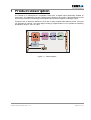
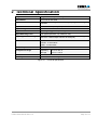
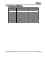
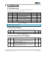
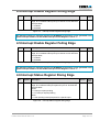
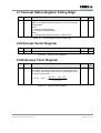
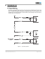
The Embedded I/O Company TIP605 16 Digital Inputs Optically Isolated Version 1.0 User Manual Issue 1.1 April 2003 D75605800 TEWS TECHNOLOGIES GmbH Am Bahnhof 7 Phone: +49-(0)4101-4058-0 e-mail: [email protected] 25469 Halstenbek / Germany Fax: +49-(0)4101-4058-19 www.tews.com TEWS TECHNOLOGIES LLC 1 E. Liberty Street, Sixth Floor Phone: +1 (775) 686 6077 e-mail: [email protected] Reno, Nevada 89504 / USA Fax: +1 (775) 686 6024 www.tews.com TIP605-10 This document contains information, which is proprietary to TEWS TECHNOLOGIES GmbH. Any reproduction without written permission is forbidden. 16 digital inputs optically isolated TEWS TECHNOLOGIES GmbH has made any effort to ensure that this manual is accurate and complete. However TEWS TECHNOLOGIES GmbH reserves the right to change the product described in this document at any time without notice. TEWS TECHNOLOGIES GmbH is not liable for any damage arising out of the application or use of the device described herein. Style Conventions Hexadecimal characters are specified with prefix 0x, i.e. 0x029E (that means hexadecimal value 029E). For signals on hardware products, an ‚Active Low’ is represented by the signal name with # following, i.e. IP_RESET#. Access terms are described as: W Write Only R Read Only R/W Read/Write R/C Read/Clear R/S Read/Set 1997-2003 by TEWS TECHNOLOGIES GmbH Issue Description Date 1.0 First Issue May 1997 1.1 General Revision April 2003 TIP605 User Manual Issue 1.2 Page 2 of 12 Table of Contents 1 2 3 4 PRODUCT DESCRIPTION ......................................................................................... 5 TECHNICAL SPECIFICATION................................................................................... 6 ID PROM CONTENTS ................................................................................................ 7 IP ADDRESSING........................................................................................................ 8 4.1 4.2 4.3 4.4 4.5 4.6 4.7 4.8 4.9 5 I/O Addressing.................................................................................................................................8 Input Data Register .........................................................................................................................8 Global Interrupt Control Register..................................................................................................8 Interrupt Enable Register Rising Edge .........................................................................................9 Interrupt Enable Register Falling Edge.........................................................................................9 Interrupt Status Register Rising Edge ..........................................................................................9 Interrupt Status Register Falling Edge .......................................................................................10 Interrupt Vector Register..............................................................................................................10 Debounce Timer Register ............................................................................................................10 INSTALLATION........................................................................................................ 11 5.1 Input Wiring ...................................................................................................................................11 6 PIN ASSIGNMENT – I/O CONNECTOR .................................................................. 12 TIP605 User Manual Issue 1.2 Page 3 of 12 Table of Figures FIGURE 1-1 : BLOCK DIAGRAM......................................................................................................................5 FIGURE 2-1 : TECHNICAL SPECIFICATION...................................................................................................6 FIGURE 3-1 : ID PROM CONTENTS ...............................................................................................................7 FIGURE 4-1 : REGISTER SET .........................................................................................................................8 FIGURE 4-2 : INPUT DATA REGISTER...........................................................................................................8 FIGURE 4-3 : GLOBAL INTERRUPT CONTROL REGISTER .........................................................................8 FIGURE 4-4 : INTERRUPT ENABLE REGISTER RISING EDGE....................................................................9 FIGURE 4-5 : INTERRUPT ENABLE REGISTER FALLING EDGE .................................................................9 FIGURE 4-6 : INTERRUPT STATUS REGISTER RISING EDGE....................................................................9 FIGURE 4-7 : INTERRUPT STATUS REGISTER FALLING EDGE ...............................................................10 FIGURE 4-8 : INTERRUPT VECTOR REGISTER..........................................................................................10 FIGURE 4-9 : DEBOUNCE TIMER REGISTER..............................................................................................10 FIGURE 5-1 : INPUT WIRING OPTIONS .......................................................................................................11 FIGURE 6-1 : INPUT I/O CONNECTION........................................................................................................12 TIP605 User Manual Issue 1.2 Page 4 of 12 1 Product Description The TIP605 is an IndustryPack compatible module with 16 digital inputs galvanically isolated by optocoupler. The individual inputs are potential free in relation to each other. A high performance input circuit ensures a defined switching point and polarization protection against confusing the pole. All inputs have an electronic debounce circuit with a freely programmable debounce time. All inputs can generate an interrupt. The signal edge handling is programmable. For the TIP605 the operating temperature range is –40°C to +85°C. Figure 1-1 : Block Diagram TIP605 User Manual Issue 1.2 Page 5 of 12 2 Technical Specification Logic Interface Single Size IndustryPack Logic I/O Interface 50-conductor flat cable Inputs 16, each input can generate an interrupt at programmable signal transition Input Isolation All channels completely independent from each other Input Voltage 24V DC Input Current 4.2mA typical @+24V input voltage Input Switching Level 12V typical (minimum 7.5, maximum 14V) Input Signal Debouncing Electronic debouncing with programmable debounce time (8µs to 261ms in 1.024ms steps common for all inputs) Wait States IOSEL: no wait states INTSEL: no wait states IDSEL: no wait states Power Requirements Tbd. Temperature Range Operating Storage MTBF 394420h Humidity 5 – 95 % non-condensing -40 °C to +85 °C -55°C to +125°C Figure 2-1 : Technical Specification TIP605 User Manual Issue 1.2 Page 6 of 12 3 ID Prom Contents Address Function Contents 0x01 ASCII ‘I’ 0x49 0x03 ASCII ‘P’ 0x50 0x05 ASCII ‘A’ 0x41 0x07 ASCII ‘C’ 0x43 0x09 Manufacturer ID 0xB3 0x0B Model Number 0x1A 0x0D Revision 0x10 0x0F Reserved 0x00 0x11 Driver-ID Low - Byte 0x00 0x13 Driver-ID High - Byte 0x00 0x15 Number of bytes used 0x0D 0x17 CRC 0x1F 0x19 Version -10 0x0A Figure 3-1 : ID PROM Contents TIP605 User Manual Issue 1.2 Page 7 of 12 4 IP Addressing 4.1 I/O Addressing The complete register set of the TIP605 is accessible in the I/O space of the IP. Address rage: ip_io_base_address + (0x00 to 0x0F) Address Symbol Description Size (Bit) Access 0x00 DATAREG Input Data Register word R 0x03 INTCONT Global Interrupt Control Register byte R/W 0x04 INTENALH Interrupt Enable Rising Edge word R/W 0x06 INTENAHL Interrupt Enable Falling Edge word R/W 0x08 INSTATLH Interrupt Status Rising Edge word R/W 0x0A INTSTATHL Interrupt Status Falling Edge word R/W 0x0D INTVEC Interrupt Vector Register byte R/W 0x0F DEBTIME Debounce Time Register byte R/W Figure 4-1 : Register Set All registers are set to ‘0’ after reset. 4.2 Input Data Register The Input Data Register is a read only register that reflects the actual states of inputs. Bit Symbol 15:0 Description Access 16 bit input data R Reset Value Figure 4-2 : Input Data Register 4.3 Global Interrupt Control Register Bit Symbol Description Access 7 Int Req Global Interrupt Request flag Read as ‘1’ = an interrupt request of at least one of the 16 input channels is pending. R 6:1 0 Reset Value Not used and undefined during reads Int Enable Global Interrupt Enable Bit 1 = globally enables interrupts for all 16 inputs on interrupt request line INTREQ0# of the IP bus R/W Figure 4-3 : Global Interrupt Control Register TIP605 User Manual Issue 1.2 Page 8 of 12 4.4 Interrupt Enable Register Rising Edge Bit Symbol 15:0 Description Access Bit 0 enables the interrupt of input channel 1 for the rising edge, bit 15 enables interrupt of input channel 16. All other bits are equivalent. 1 = enabled 0 = disabled R/W Reset Value Figure 4-4 : Interrupt Enable Register Rising Edge An interrupt request on interrupt request line INTREQ0# of the IP bus is only generated if the global interrupt enable bit of the Global Interrupt Control Register is set to ‘1’. 4.5 Interrupt Enable Register Falling Edge Bit Symbol 15:0 Description Access Bit 0 enables the interrupt of input channel 1 for the falling edge, bit 15 enables interrupt of input channel 16. All other bits are equivalent. 1 = enabled 0 = disabled R/W Reset Value Figure 4-5 : Interrupt Enable Register Falling Edge An interrupt request on interrupt request line INTREQ0# of the IP bus is only generated if the global interrupt enable bit of the Global Interrupt Control Register is set to ‘1’. 4.6 Interrupt Status Register Rising Edge Bit 15:0 Symbol Description Access Bit 0 reflects the interrupt request state of input 1 for the rising edge, bit 15 reflects interrupt request of input 16. All other bits are equivalent. Read: 1 = interrupt request pending 0 = no interrupt request pending Write: 1 = clear pending interrupt request for a specific input R/W Reset Value Figure 4-6 : Interrupt Status Register Rising Edge TIP605 User Manual Issue 1.2 Page 9 of 12 4.7 Interrupt Status Register Falling Edge Bit Symbol 15:0 Description Access Bit 0 reflects the interrupt request state of input 1 for the falling edge, bit 15 reflects interrupt request of input 16. All other bits are equivalent. Read: 1 = interrupt request pending 0 = no interrupt request pending Write: 1 = clear pending interrupt request for a specific input R/W Reset Value Figure 4-7 : Interrupt Status Register Falling Edge 4.8 Interrupt Vector Register Bit Symbol 7:0 Description Access 8 bit interrupt vector is loaded by software R/W Reset Value Figure 4-8 : Interrupt Vector Register 4.9 Debounce Timer Register Bit 7:0 Symbol Description Access Value 0 sets the debounce time to a minimum of 8µs (default after reset). The debounce time can be programmed in steps of 1.024ms in the range of 8µs to 261ms. The debounce time is common for all inputs. R/W preload value = Reset Value debounce time ( ms ) 1 . 024 ( ms ) Figure 4-9 : Debounce Timer Register TIP605 User Manual Issue 1.2 Page 10 of 12 5 Installation 5.1 Input Wiring Each input is optically isolated from the logic circuit. Each input is independent of the other inputs and can be wired different. Each input has two connections at the IP I/O connector, input x+ and input x-. All inputs are isolated by optocoupler and against each other. The input channels can be activated only in one polarity and have an external diode to prevent damage of the optocoupler by wiring the input in a wrong direction. Figure 5-1 : Input Wiring Options TIP605 User Manual Issue 1.2 Page 11 of 12 6 Pin Assignment – I/O Connector Pin Function 1 Input 1 + 2 Input 1 - 3 Input 2 + 4 Input 2 - 5 Input 3 + 6 Input 3 - 7 Input 4 + 8 Input 4 - 9 Input 5 + 10 Input 5 - 11 Input 6 + 12 Input 6 - 13 Input 7 + 14 Input 7 - 15 Input 8 + 16 Input 8 - 17 Input 9 + 18 Input 9 - 19 Input 10 + 20 Input 10 - 21 Input 11 + 22 Input 11 - 23 Input 12 + 24 Input 12 - 25 Input 13 + 26 Input 13 - 27 Input 14 + 28 Input 14 - 29 Input 15 + 30 Input 15 - 31 Input 16 + 32 Input 16 - Figure 6-1 : Input I/O Connection TIP605 User Manual Issue 1.2 Page 12 of 12