1
INTERFACING TO DSPS
SECTION 8
INTERFACING TO DSPs
Walt Kester, Dan King
INTRODUCTION
As the technology in the rapidly growing field of mixed signal processing evolves,
more highly integrated DSP products are being introduced (such as the ADSP21ESP202) which contain on-chip ADCs and DACs as well as the DSP, thereby
eliminating most component-level interface problems. Stand-alone ADCs and DACs
are now available with interfaces especially designed for DSP chips, thereby
minimizing or eliminating external interface support or glue logic. High
performance sigma-delta ADCs and DACs are currently available in the same
package (called a CODEC or COder/DECcoder) such as the AD73311 and AD73322.
These products are also designed to require minimum glue logic when interfacing to
the most common DSP chips. This section discusses the various data transfer and
timing issues associated with the various interfaces.
PARALLEL INTERFACING TO DSP PROCESSORS:
READING DATA FROM MEMORY-MAPPED PERIPHERAL
ADCS
Interfacing an ADC or a DAC to a fast DSP parallel requires an understanding of
how the DSP processor reads data from a memory-mapped peripheral (the ADC)
and how the DSP processor writes data to a memory-mapped peripheral (the DAC).
We will first consider some general timing requirements for reading and writing
data. It should be noted that the same concepts presented here regarding ADCs and
DACs apply equally when reading and writing from/to external memory.
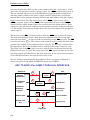
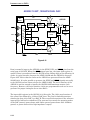
A block diagram of a typical parallel DSP interface to an external ADC is shown in
Figure 8.1. This diagram has been greatly simplified to show only those signals
associated with reading data from an external memory-mapped peripheral device.
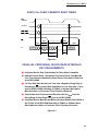
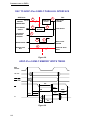
The timing diagram for the ADSP-21xx read-cycle is shown in Figure 8.2.
In this example it is assumed that the ADC is sampling at a continuous rate which
is controlled by the external sampling clock, not the internal DSP clock. Using a
separate clock for the ADC is the preferred method, since the DSP clock may be
noisy and introduce jitter in the ADC sampling process, thereby increasing the noise
level.
Assertion of the sampling clock at the ADC convert start input initiates the
conversion process (step 1). The leading (or trailing) edge of this pulse causes the
internal ADC sample-and-hold to switch from the sampling mode to the hold mode
so that the conversion process can take place. When the conversion is complete, the
conversion complete output of the ADC is asserted (step 2). The read process thus
begins when this signal is applied to the processor interrupt request line ( IRQ ) of
the DSP. The processor then places the address of the peripheral initiating the
8.1