1
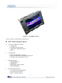
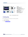
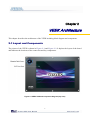
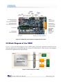
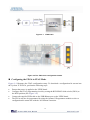
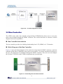
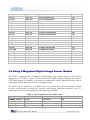
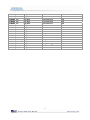
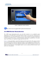
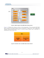
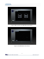
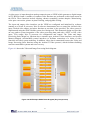
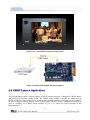
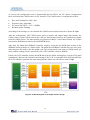
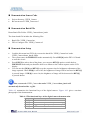
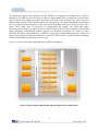
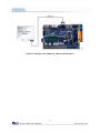
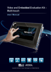
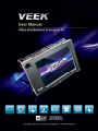
1 CONTENTS CHAPTER 1 INTRODUCTION OF THE VEEK...................................................................................................... 3 1.1 ABOUT THE KIT ......................................................................................................................................................... 7 1.2 GETTING HELP .......................................................................................................................................................... 8 CHAPTER 2 VEEK ARCHITECTURE.........................................................................................................9 2.1 LAYOUT AND COMPONENTS ...................................................................................................................................... 9 2.2 BLOCK DIAGRAM OF THE VEEK............................................................................................................................. 10 CHAPTER 3 USING THE VEEK ............................................................................................................... 11 3.1 CONFIGURING THE CYCLONE IV E FPGA............................................................................................................... 11 3.2 BUS CONTROLLER .................................................................................................................................................. 14 3.3 USING THE 8” LCD TOUCH SCREEN MODULE ........................................................................................................ 15 3.4 USING 5-MEGAPIXEL DIGITAL IMAGE SENSOR MODULE ........................................................................................ 16 CHAPTER 4 VEEK DEMONSTRATIONS .................................................................................................18 4.1 SYSTEM REQUIREMENTS ......................................................................................................................................... 18 4.2 FACTORY CONFIGURATION ...................................................................................................................................... 18 4.3 VEEK STARTER DEMONSTRATION .......................................................................................................................... 19 4.4 VEEK PICTURE VIEWER ......................................................................................................................................... 23 4.5 VIDEO AND IMAGE PROCESSING.............................................................................................................................. 26 4.6 VEEK CAMERA APPLICATION ................................................................................................................................. 29 4.7 VIDEO AND IMAGE PROCESSING FOR CAMERA ........................................................................................................ 32 1 CHAPTER 5 APPLICATION SELECTOR .................................................................................................36 5.1 READY TO RUN SD CARD DEMOS ........................................................................................................................... 36 5.2 RUNNING THE APPLICATION SELECTOR................................................................................................................... 37 5.3 APPLICATION SELECTOR DETAILS ........................................................................................................................... 37 5.4 RESTORING THE FACTORY IMAGE ........................................................................................................................... 40 CHAPTER 6 APPENDIX ...........................................................................................................................42 6.1 REVISION HISTORY ................................................................................................................................................. 42 6.2 COPYRIGHT STATEMENT ......................................................................................................................................... 42 2 Chapter 1 Introduction of the VEEK The VEEK FPGA Development Kit is a comprehensive design environment with everything embedded developers need to create processing-based systems. The VEEK delivers an integrated platform that includes hardware, design tools, intellectual property (IP) and reference designs for developing embedded software and hardware platform in a wide range of applications. The fully integrated kit allows developers to rapidly customize their processor and IP to best suit their specific application. The VEEK features the DE2-115 development board targeting the Cyclone IV E FPGA, as well as a LCD multimedia color touch panel and a 5-Megapixel digital image sensor module. The VEEK is preconfigured with an FPGA hardware reference design including several Ready-to-Run demonstration applications stored on the provided SD-Card. Software developers can use these reference designs as their platform to quickly architect, develop and build complex embedded systems. By simply scrolling through the demo of your choice on the LCD multimedia color touch panel, you can evaluate numerous processor system designs. The all-in-one embedded solution offered on the VEEK, in combination of the LCD touch panel and digital image module, provide embedded developers the ideal platform for multimedia applications with unparallel processing performance. Developers can benefit from the use of FPGA-based embedded processing system such as mitigate design risk and obsolescence, design reuse, reducing bill of material (BOM) costs by integrating powerful graphics engines within the FPGA, and lower cost. Figure 1-1 shows a photograph of the VEEK. 3 Figure 1-1 The VEEK overview The key features of the board are listed below: DE2-115 Development Board • Cyclone IV EP4CE115 FPGA o 114,480 LEs o 432 M9K memory blocks o 3,888 Kbits embedded memory o 4 PLLs • Configuration o On-board USB-Blaster circuitry o JTAG and AS mode configuration supported o EPCS64 serial configuration device • Memory Devices o 128MB SDRAM o 2MB SRAM o 8MB Flash with 8-bit mode o 32Kbit EEPROM • Switches and Indicators o 18 switches and 4 push-buttons o 18 red and 9 green LEDs o Eight 7-segment displays 4 • Audio o 24-bit encoder/decoder (CODEC) o Line-in, line-out, and microphone-in jacks • Display o 16x2 LCD module • On-Board Clocking Circuitry o Three 50MHz oscillator clock inputs o SMA connectors (external clock input/output) • SD Card Socket o Provides SPI and 4-bit SD mode for SD Card access • Two Gigabit Ethernet Ports o Integrated 10/100/1000 Gigabit Ethernet • High Speed Mezzanine Card (HSMC) o Configurable I/O standards (voltage levels: 3.3/2.5/1.8/1.5V) • USB Type A and B o Provide host and device controller compliant with USB 2.0 o Support data transfer at full-speed and low-speed o PC driver available • 40-pin Expansion Port o Configurable I/O standards (voltage levels: 3.3/2.5/1.8/1.5V) • VGA-out Connector o VGA DAC (high speed triple DACs) • DB9 Serial Connector o RS232 port with flow control • PS/2 Connector o PS/2 connector for connecting a PS2 mouse or keyboard • TV-in Connector o TV decoder (NTSC/PAL/SECAM) • Remote Control o Infrared receiver module 5 • Power o Desktop DC input o Switching and step-down regulators LM3150MH LCD touch screen module • • • • Equipped with an 8-inch Amorphous-TFT-LCD (Thin Film Transistor Liquid Crystal Display) module Module composed of LED backlight Support 18-bit parallel RGB interface Converting the X/Y coordination of touch point to its corresponding digital data via the Analog Devices AD7843 A/D converter Table 1-1 shows the general physical specifications of the LTC (Note*). Table 1-1 General physical specifications of the LCD Item Specification Unit LCD size 8 inch (Diagonal) - Resolution 800 x3(RGB) x 600 dot Dot pitch 0.0675(W) x 0.2025(H) mm Active area 162.0(W) x 121.5(H) mm Module size 183.0(W) x 141.0(H) x 7.2(D) mm Surface treatment Anti-Glare - Color arrangement RGB-stripe - Interface Digital - 5-Megapixel digital image sensor module • • • • • • • • • • • Superior low-light performance High frame rate Low dark current Global reset release, which starts the exposure of all rows simultaneously Bulb exposure mode, for arbitrary exposure times Snapshot mode to take frames on demand Horizontal and vertical mirror image Column and row skip modes to reduce image size without reducing field-of-view Column and row binning modes to improve image quality when resizing Simple two-wire serial interface Programmable controls: gain, frame rate, frame size, exposure Table 1-2 shows the key parameters of the CMOS sensor (Note*). 6 Table 1-2 Key performance parameters of the CMOS sensor Parameter Value Active Pixels 2592Hx1944V Pixel size 2.2umx2.2um Color filter array RGB Bayer pattern Shutter type Global reset release(GRR) Maximum data rate/master clock 96Mp/s at 96MHz Frame rate Full resolution Programmable up to 15 fps VGA mode Programmable up to 70 fps ADC resolution 12-bit Responsivity 1.4V/lux-sec(550nm) Pixel dynamic range 70.1dB SNRMAX 38.1dB Supply Voltage Power I/O 3.3V 1.7V~3.1V Note: for more detailed information of the LCD touch panel and CMOS sensor module, please refer to their datasheets respectively. 1.1 About the Kit The kit contains all users needed to run the demonstrations and develop custom designs, as shown in Figure 1-2. The system CD contains technical documents of the VEEK which includes component datasheets, demonstrations, schematic, and user manual. 7 Figure 1-2 VEEK kit package contents 1.2 Getting Help Here is information of how to get help if you encounter any problem: • • • Terasic Technologies Tel: +886-3-550-8800 Email: [email protected] 8 Chapter 2 VEEK Architecture This chapter describes the architecture of the VEEK including block diagram and components. 2.1 Layout and Components The picture of the VEEK is shown in Figure 2-1 and Figure 2-2. It depicts the layout of the board and indicates the locations of the connectors and key components. Figure 2-1 VEEK PCB and component diagram (top view) 9 Figure 2-2 VEEK PCB and component diagram (bottom view) 2.2 Block Diagram of the VEEK Figure 2-3 gives the block diagram of the VEEK board. To provide maximum flexibility for the user, all connections are made through the Cyclone IV E FPGA device. Thus, the user can configure the FPGA to implement any system design. Figure 2-3 Block Diagram of VEEK 10 Chapter 3 Using the VEEK This section describes the detailed information of the components, connectors, and pin assignments of the VEEK. 3.1 Configuring the Cyclone IV E FPGA The VEEK board contains a serial configuration device that stores configuration data for the Cyclone IV E FPGA. This configuration data is automatically loaded from the configuration device into the FPGA every time while power is applied to the board. Using the Quartus II software, it is possible to reconfigure the FPGA at any time, and it is also possible to change the non-volatile data that is stored in the serial configuration device. Both types of programming methods are described below. 1. JTAG programming: In this method of programming, named after the IEEE standards Joint Test Action Group, the configuration bit stream is downloaded directly into the Cyclone IV E FPGA. The FPGA will retain this configuration as long as power is applied to the board; the configuration information will be lost when the power is turned off. 2. AS programming: In this method, called Active Serial programming, the configuration bit stream is downloaded into the Altera EPCS64 serial configuration device. It provides non-volatile storage of the bit stream, so that the information is retained even when the power supply to the VEEK board is turned off. When the board’s power is turned on, the configuration data in the EPCS64 device is automatically loaded into the Cyclone IV E FPGA. JTAG Chain on VEEK Board To use JTAG interface for configuring FPGA device, the JTAG chain on the VEEK must form a close loop that allows Quartus II programmer to detect the FPGA device. Figure 3-1 illustrates the JTAG chain on the VEEK board. Shorting pin1 and pin2 on JP3 can disable the JTAG signals on the HSMC connector that will form a close JTAG loopback on DE2-115 (See Figure 3-2). Thus, only the on board FPGA device (Cyclone IV E) will be detected by Quartus II programmer. By default, a jumper is placed on pin1 and pin3 of JP3. To prevent any changes to the bus controller (Max II EPM240) described in later sections, users should not adjust the jumper on JP3. 11 Figure 3-1 JTAG Chain Figure 3-2 The JTAG chain configuration header Configuring the FPGA in JTAG Mode Figure 3-3 illustrates the JTAG configuration setup. To download a configuration bit stream into the Cyclone IV E FPGA, perform the following steps: • • • • Ensure that power is applied to the VEEK board Configure the JTAG programming circuit by setting the RUN/PROG slide switch (SW19) to the RUN position (See Figure 3-4) Connect the supplied USB cable to the USB-Blaster port on the VEEK board The FPGA can now be programmed by using the Quartus II Programmer module to select a configuration bit stream file with the .sof filename extension 12 Figure 3-3 The JTAG chain configuration scheme Figure 3-4 The RUN/PROG switch (SW19) is set to JTAG mode Configuring the EPCS64 in AS Mode Figure 3-5 illustrates the AS configuration set up. To download a configuration bit stream into the EPCS64 serial configuration device, perform the following steps: • • • • • Ensure that power is applied to the VEEK board Connect the supplied USB cable to the USB-Blaster port on the VEEK board Configure the JTAG programming circuit by setting the RUN/PROG slide switch (SW19) to the PROG position The EPCS64 chip can now be programmed by using the Quartus II Programmer module to select a configuration bit stream file with the .pof filename extension Once the programming operation is finished, set the RUN/PROG slide switch back to the RUN position and then reset the board by turning the power switch off and back on; this action causes the new configuration data in the EPCS64 device to be loaded into the FPGA chip 13 Figure 3-5 The AS configuration scheme 3.2 Bus Controller The VEEK comes with a bus controller using the Max II EPM240 that allows user to access the touch screen module through the HSMC connector. This section describes its structure in block diagram form and its capabilities. Bus Controller Introduction The bus controller provides level shifting functionality from 2.5V (HSMC) to 3.3V domains. Block Diagram of the Bus Controller Figure 3-6 gives the block diagram of the connection setup from the HSMC connector to the bus controller on the Max II EPM240 to the touch screen module. To provide maximum flexibility for the user, all connections are established through the HSMC connector. Thus, the user can configure the Cyclone IV E FPGA on the VEEK to implement any system design. Figure 3-6 Block Diagram of the Bus Controller 14 3.3 Using the 8” LCD Touch Screen Module The VEEK features an 8-inch Amorphous-TFT-LCD panel. The LCD Touch Screen module offers resolution of (800x600) to provide users the best display quality for developing applications. The LCD panel supports 18-bit parallel RGB data interface. The VEEK is also equipped with an Analog Devices AD7843 touch screen digitizer chip. The AD7843 is a 12-bit analog to digital converter (ADC) for digitizing x and y coordinates of touch points applied to the touch screen. The coordinates of the touch points can be read through the serial port interface on the AD7843. To display images on the LCD panel correctly, the RGB color data along with the data enable and clock signals must act according to the timing specification of the LCD touch panel as shown in Table 3-1. Table 3-2 gives the pin assignment information of the LCD touch panel. Table 3-1 LCD timing specifications Parameter Symbol CLK Frequency CLK Period CLK Pulse Duty DE Period DE Pulse Width DE Frame Blanking DE Frame Width OEV Pulse Width OKV Pulse Width DE(internal)-STV Time DE(internal)-CKV Time DE(internal)-OEV Time DE(internal)-POL Time STV Pulse Width Min. FCPH FCPH FCWH FDEH+ TDEL FDH FHS FEP TOEV TCKV T1 T2 T3 T4 - 40 1000 10 - Values Typ. 39.79 25.13 50 1056 800 28 600 150 133 4 40 23 157 1 Max. 60 110 - Unit MHz Ns % TCPH TCPH FDEH+TDEL FDEH+TDEL TCPH TCPH TCPH TCPH TCPH TCPH TH Note: THS + THA < TH Table 3-2 Pin assignment of the LCD touch panel Signal Name FPGA Pin No. Description I/O Standard LCD_DIM LCD_NCLK LCD_R0 LCD_R1 PIN_P27 PIN_V24 PIN_V26 PIN_R27 LCD backlight enable LCD clock LCD red data bus bit 0 LCD red data bus bit 1 2.5V 2.5V 2.5V 2.5V 15 LCD_R2 LCD_R3 LCD_R4 LCD_R5 LCD_G0 LCD_G1 LCD_G2 LCD_G3 LCD_G4 LCD_G5 LCD_B0 LCD_B1 LCD_B2 LCD_B3 LCD_B4 LCD_B5 LCD _DEN TOUCH _PENIRQ_N TOUCH _DOUT TOUCH _BUSY TOUCH _DIN TOUCH _CS_N TOUCH _DCLK PIN_R28 PIN_U27 PIN_U28 PIN_V27 PIN_P21 PIN_R21 PIN_R22 PIN_R23 PIN_T21 PIN_T22 PIN_V28 PIN_U22 PIN_V22 PIN_V25 PIN_L28 PIN_J26 PIN_P25 PIN_L22 PIN_L21 PIN_U26 PIN_U25 PIN_T26 PIN_T25 LCD red data bus bit 2 LCD red data bus bit 3 LCD red data bus bit 4 LCD red data bus bit 5 LCD green data bus bit 0 LCD green data bus bit 1 LCD green data bus bit 2 LCD green data bus bit 3 LCD green data bus bit 4 LCD green data bus bit 5 LCD blue data bus bit 0 LCD blue data bus bit 1 LCD blue data bus bit 2 LCD blue data bus bit 3 LCD blue data bus bit 4 LCD blue data bus bit 5 LCD RGB data enable AD7843 pen interrupt AD7843 serial interface data out AD7843 serial interface busy AD7843 serial interface data in AD7843 serial interface chip select input AD7843 interface clock 2.5V 2.5V 2.5V 2.5V 2.5V 2.5V 2.5V 2.5V 2.5V 2.5V 2.5V 2.5V 2.5V 2.5V 2.5V 2.5V 2.5V 2.5V 2.5V 2.5V 2.5V 2.5V 2.5V 3.4 Using 5-Megapixel Digital Image Sensor Module The VEEK is equipped with a 5-Megapixel digital image sensor module that provides an active imaging array of 2,592H x 1,944V. It features low-noise CMOS imaging technology that achieves CCD image quality. In addition, it incorporates sophisticated camera functions on-chip such as windowing, column and row skip mode, and snapshot mode. The sensor can be operated in its default mode or programmed by the user through a simple two-wire serial interface for frame size, exposure, gain settings, and other parameters. Table 3-3 contains the pin names and descriptions of the image sensor module. Table 3-3 Pin assignment of the CMOS sensor Signal Name CAMERA_ PIXCLK CAMERA_ D0 CAMERA_ D1 CAMERA_ D2 FPGA Pin No. PIN_J27 PIN_F26 PIN_E26 PIN_G25 Description Pixel clock Pixel data bit 0 Pixel data bit 1 Pixel data bit 2 16 I/O Standard 2.5V 2.5V 2.5V 2.5V CAMERA_ D3 PIN_G26 CAMERA_ D4 PIN_H25 CAMERA_ D5 PIN_H26 CAMERA_ D6 PIN_K25 CAMERA_ D7 PIN_K26 CAMERA_ D8 PIN_L23 CAMERA_ D9 PIN_L24 CAMERA_ D10 PIN_M25 CAMERA_ D11 PIN_M26 CAMERA_ STROBE PIN_G28 CAMERA_ LVAL PIN_K27 CAMERA_ FVAL PIN_K28 CAMERA_ RESET_N PIN_M28 CAMERA_ SCLK PIN_K22 CAMERA_ TRIGGER PIN_H23 CAMERA_ SDATA PIN_H24 CAMERA_ XCLKIN PIN_G23 Pixel data bit 3 Pixel data bit 4 Pixel data bit 5 Pixel data bit 6 Pixel data bit 7 Pixel data bit 8 Pixel data bit 9 Pixel data bit 10 Pixel data bit 11 Snapshot strobe Line valid Frame valid Image sensor reset Serial clock Snapshot trigger Serial data External input clock 17 2.5V 2.5V 2.5V 2.5V 2.5V 2.5V 2.5V 2.5V 2.5V 2.5V 2.5V 2.5V 2.5V 2.5V 2.5V 2.5V 2.5V Chapter 4 VEEK Demonstrations This chapter gives detailed description of the provided bundles of exclusive demonstrations implemented on VEEK. These demonstrations are particularly designed (or ported) for VEEK, with the goal of showing the potential capabilities of the kit and showcase the unique benefits of FPGA-based SOPC systems such as reducing BOM costs by integrating powerful graphics and video processing circuits within the FPGA. 4.1 System Requirements To run and recompile the demonstrations, you should: • • • Install Altera Quartus II 10.0 and NIOS II EDS 10.0 or later edition on the host computer Install the USB-Blaster driver software. You can find instructions in the tutorial “Getting Started with Altera’s DE2-115 Board” (tut_initialDE2-115.pdf) which is available on the DE2-115 system CD Copy the entire demonstrations folder from the VEEK system CD to your host computer 4.2 Factory Configuration The VEEK development kit comes preconfigured with a default utility that boots up on power on and allows users to quickly select, load, and run different Ready-to-Run demonstrations stored on an SD Card using the VEEK touch panel. Figure 4-1 gives a snapshot of the default application selector interface (Note*). Every demonstration consists of a FPGA hardware image and an application software image. When you select a demonstration the application selector copies the hardware image to EPCS device and software image to flash memory and reconfigures the FPGA with your selection. For more comprehensive information of the application selector factory configuration, please refer to chapter 5. 18 Figure 4-1 Application selector interface Note: Please insert the supplied SD Card from this demonstration. 4.3 VEEK Starter Demonstration The VEEK starter demonstration takes user the initial experience of an embedded system integrating a LCD Touch Panel. This demonstration consists of two sub item, Touch and Color pattern generator. The Touch segment draws a circle on where you touch the screen and updates its coordinates on the top left corner. The pattern generator can be treated as an upgrade version of the LCD test program. The software successively generates different color patterns after a fixed time delay. Users could use it to quickly investigate any flaw of the LCD. Figure 4-2 shows the hardware system block diagram of this demonstration. The system is clocked by an external 50MHz Oscillator. Through the internal PLL module, the generated 100MHz clock is used for Nios II processor and other components, and there also a 40MHz pixel clock for the video pipeline and 10MHz for low-speed peripherals. The Nios II CPU runs the application software and controls all the peripherals. A scatter-gather DMA is used to transfer pixel data from the video buffer to the video pipeline. 19 Figure 4-2 Block diagram of the VEEK Starter demonstration Figure 4-3 illustrates the software structure of this demonstration. The touch panel’s SPI HAL block responds to the bottom hardware requests and interface to upper layers. The SGDMA HAL allocates required frame/descriptor buffers to specified memory address and is responsible of handling frame buffer update issue. Figure 4-3 Software stack of the VEEK Starter demonstration 20 Demonstration Source Code • • • Project directory: VEEK_Starter Bit stream used: VEEK_Starter.sof Nios II Workspace: VEEK_Starter\Software Demonstration Batch File Demo Batch File Folder:VEEK_Starter\demo_batch The demo batch file includes the following files: • • • Batch File: VEEK_Starter.bat, VEEK_Starter_bashrc FPGA Configure File: VEEK_Starter.sof Nios II Program: VEEK_Starter.elf Demonstration Setup • • • • • • • Make sure Quartus II and Nios II are installed on your PC Power on the DE2-115 board Connect USB-Blaster to the DE2-115 board and install USB-Blaster driver if necessary Execute the demo batch file “VEEK_Starter.bat” under the batch file folder, VEEK_Starter\demo_batch After Nios II program is downloaded and executed successfully, a prompt message will be displayed in nios2-terminal From on the touch panel, tap any icon of the main interface and start the experience, as shown in Figure 4-4, Figure 4-5 and Figure 4-6 Under each sub item, touch the Exit button on the left bottom corner will lead you back to the main interface 21 Figure 4-4 Main interface of the VEEK Starter demonstration Figure 4-5 The VEEK Starter Touch sub item 22 Figure 4-6 The VEEK Starter Pattern sub item 4.4 VEEK Picture Viewer This demonstration shows a simple picture viewer implementation using Nios II based SOPC system. It reads JPEG images stored on SD Card and displays them on the LCD. The Nios II CPU decodes the images and fills the raw result data into frame buffers in SDRAM. The VEEK will show the image the buffer being displayed points to. When users touch the LCD Touch Panel, it will proceed to display the next buffered image until there is no filled buffer and enter the Loading phase. Figure 4-7 shows the block diagram of this demonstration. The Nios II CPU here takes a key roll in the demonstration. It is responsible of decoding the JPEG images and coordinates the works of all the peripherals. The touch panel handling program uses the timer as a regular interrupter and periodically updates the pen state and sampled coordinates. 23 Figure 4-7 Block diagram of the picture viewer demonstration Demonstration Source Code • • • Project directory: VEEK_Picture_Viewer Bit stream used: VEEK_Picture_Viewer.sof Nios II Workspace: VEEK_Picture_Viewer\Software Demonstration Batch File Demo Batch File Folder: VEEK_Picture_Viewer\demo_batch The demo batch file includes the following files: • • • Batch File: VEEK_Picture_Viewer.bat, VEEK_Picture_Viewer _bashrc FPGA Configure File: VEEK_Picture_Viewer.sof Nios II Program: VEEK_Picture_Viewer.elf Demonstration Setup • • • • Format your SD Card into FAT16 format Place the jpg image files to the \jpg subdirectory of the SD Card. For best display result, the image should have a resolution of 800x600 or the multiple of that Insert the SD Card to the SD Card slot on the VEEK Load the bitstream into the FPGA on the VEEK board 24 • • Run the Nios II Software under the workspace VEEK_Picture_Viewer\Software (Note*) Touch the play button will proceed to display the next image. Figure 4-8 gives a screen shot of the VEEK picture viewer demonstration. Table 4-1 shows the instructions for running the demonstration Figure 4-8 VEEK picture viewer demonstration Table 4-1 Touch panel displayed information Display information Implication Press the play button to display the next buffered image Indicates the loading progress Note: execute the VEEK_Picture_Viewer.bat under VEEK_Picture_Viewer\demo_batch will automatically download the .sof and .elf file. 25 4.5 Video and Image Processing The Video and Image Processing (VIP) Example Design demonstrates dynamic scaling and clipping of a standard definition video stream in either National Television System Committee (NTSC) or Phase Alternation Line (PAL) format and picture-in-picture mixing with a background layer. The video stream is output in high definition resolution (800×600) on the HSMC LTC daughter card (part of the VEEK). The example design demonstrates a framework for rapid development of video and image processing systems using the parameterizable MegaCore® functions that are available in the Video and Image Processing Suite. Available functions are listed in Table 4-2. This demonstration needs the Quartus II license file includes the VIP suite feature. Table 4-2 VIP IP cores functions IP MegaCore Function Frame Reader Control Synchronizer Switch Color Space Converter Chroma Resampler 2D FIR Filter Alpha Blending Mixer Scaler Deinterlacer Test Pattern Generator Clipper Color Plane Sequencer Frame Buffer 2D Median Filter Gamma Corrector Clocked Video Input/Output Description Reads video from external memory and outputs it as a stream. Synchronizes the changes made to the video stream in real time between two functions. Allows video streams to be switched in real time. Converts image data between a variety of different color spaces such as RGB to YCrCb. Changes the sampling rate of the chroma data for image frames, for example from 4:2:2 to 4:4:4 or 4:2:2 to 4:2:0. Implements a 3 x 3, 5 x 5, or 7 x 7 finite impulse response (FIR) filter on an image data stream to smooth or sharpen images. Mixes and blends multiple image streams—useful for implementing text overlay and picture-in-picture mixing. A sophisticated polyphase scaler that allows custom scaling and real-time updates of both the image sizes and the scaling coefficients. Converts interlaced video formats to progressive video format using a motion adaptive deinterlacing algorithm. Also supports 'bob' and "weave" algorithms Generates a video stream that contains still color bars for use as a test pattern. Provides a way to clip video streams and can be configured at compile time or at run time. Changes how color plane samples are transmitted across the Avalon-ST interface. This function can be used to split and join video streams, giving control over the routing of color plane samples. Buffers video frames into external RAM. This core supports double or triple-buffering with a range of options for frame dropping and repeating. Provides a way to apply 3 x 3, 5 x 5, or 7 x 7 pixel median filters to video images. Allows video streams to be corrected for the physical properties of display devices. These two cores convert the industry-standard clocked video format (BT-656) to Avalon-ST video and vice versa. These functions allow you to fully integrate common video functions with video interfaces, processors, and external memory controllers. The example design uses an Altera Cyclone® IV E EP4CE115F29 featured VEEK board. 26 A video source is input through an analog composite port on VEEK which generates a digital output in ITU BT656 format. A number of common video functions are performed on this input stream in the FPGA. These functions include clipping, chroma resampling, motion adaptive deinterlacing, color space conversion, picture-in-picture mixing, and polyphase scaling. The input and output video interfaces on the VEEK are configured and initialized by software running on a Nios® II processor. Nios II software demonstrates how to control the clocked video input, clocked video output, and mixer functions at run-time is also provided. The video system is implemented using the SOPC Builder system level design tool. This abstracted design tool provides an easy path to system integration of the video processing data path with a NTSC or PAL video input, VGA output, Nios II processor for configuration and control. The Video and Image Processing Suite MegaCore functions have common open Avalon-ST data interfaces and Avalon Memory-Mapped (Avalon-MM) control interfaces to facilitate connection of a chain of video functions and video system modeling. In addition, video data is transmitted between the Video and Image Processing Suite functions using the Avalon-ST Video protocol, which facilitates building run-time controllable systems and error recovery. Figure 4-9 shows the Video and Image Processing block diagram. Figure 4-9 VIP Example SOPC Block Diagram (Key Components) 27 Demonstration Source Code • • • Project directory: VEEK_VIP Bit stream used: VEEK_VIP.sof Nios II Workspace: VEEK_VIP\Software Demonstration Batch File Demo Batch File Folder: VEEK_VIP\demo_batch The demo batch file includes the following files: • • • Batch File: VEEK_VIP.bat, VEEK_VIP_bashrc FPGA Configure File: VEEK_VIP.sof Nios II Program: VEEK_VIP.elf Demonstration Setup • • • • • Connect a DVD player’s composite video output(yellow plug) to the Video-IN RCA jack(J12) of the VEEK board. The DVD player has to be configured to provide NTSC output or PAL output Connect the VGA output of the VEEK board to a VGA monitor (both LCD and CRT type of monitors should work) Load the bit stream into FPGA (note*) Run the Nios II and choose VEEK_VIP\Software as the workspace. Click on the Run button (note *) Press and drag the video frame box will result in scaling the playing window to any size, as shown in Figure 4-10 Note: (1).Execute VEEK_VIP\demo_batch\VEEK _VIP.bat will download .sof and .elf files. (2).You may need additional Altera VIP suite Megacore license features to recompile the project. Figure 4-11 illustrates the setup for this demonstration. 28 Figure 4-10 The VIP demonstration running result Figure 4-11 Setup for the VEEK_VIP demonstration 4.6 VEEK Camera Application This demonstration shows a digital camera reference design using the 5-Megapixel CMOS sensor and 8-inch LCD modules on the VEEK. The CMOS sensor module sends the raw image data to FPGA on DE2-115 Board, the FPGA on the board is handling image processing part and converts the data to RGB format to display on the LCD module. The I2C Sensor Configuration module is used to configure the CMOS sensor module. Figure 4-12 shows the block diagram of the demonstration. 29 As soon as the configuration code is downloaded into the FPGA, the I2C Sensor Configuration block will initial the CMOS sensor via I2C interface. The CMOS sensor is configured as follow: • • • • Row and Column Size: 800 * 600 Exposure time: Adjustable Pix clock: MCLK*2 = 25*2 = 50MHz Readout modes: Binning According to the settings, we can calculate the CMOS sensor output frame rate is about 44.4 fps. After the configuration, The CMOS sensor starts to capture and output image data streams, the CMOS sensor Capture block extracts the valid pix data streams based on the synchronous signals from the CMOS sensor. The data streams are generated in Bayer Color Pattern format. So it’s then converted to RGB data streams by the RAW2RGB block. After that, the Multi-Port SDRAM Controller acquires and writes the RGB data streams to the SDRAM which performs as a frame buffer. The Multi-Port SDRAM Controller has two write ports and read ports also with 16-bit data width each. The writing clock is the same as CMOS sensor pix clock, and the reading clock is provided by the LCD Controller, which is 40MHz. Finally, the LCD controller fetches the RGB data from the buffer and displays it on the LCD panel continuously. Because the resolution and timing of the LCD is compatible with SVGA@800*600, the LCD controller generates the same timing and the frame rate can achieve about 25 fps. Figure 4-12 Block diagram of the digital camera design 30 Demonstration Source Code • • Project directory: VEEK_Camera Bit stream used: VEEK_Camera.sof Demonstration Batch File Demo Batch File Folder: VEEK_Camera\demo_batch The demo batch file includes the following files: • • Batch File: VEEK_Camera.bat FPGA Configure File: VEEK_Camera.sof Demonstration Setup • • • • Load the bit stream into FPGA by execute the batch file ‘VEEK_Camera.bat’ under VEEK_Camera\demo_batch\ folder The system enters the FREE RUN mode automatically. Press KEY[0] on the DE2-115 board to reset the circuit Press KEY[2] to take a shot of the photo; you can press KEY[3] again to switch back to FREE RUN mode and you should be able to see whatever the camera captures on the LCD display User can use the SW[0] and KEY[1] to set the exposure time for brightness adjustment of the image captured. When SW[0] is set to Off, the brightness of image will be increased as KEY[1] is pressed longer. If SW[0] is set to On, the brightness of image will be decreased as KEY[1] is pressed shorter Note: execute the VEEK_Camera.bat under VEEK_Camera\demo_batch will automatically download the .sof file. Table 4-3 summarizes the functional keys of the digital camera. Figure 4-13 gives a run-time photograph of the demonstration. Table 4-3 The functional keys of the digital camera demonstration Component Function Description KEY[0] Reset circuit KEY[1] Set the new exposure time (use with SW[0] ) KEY[2] Trigger the Image Capture (take a shot) KEY[3] Switch to Free Run mode 31 SW[0] HEX[7:0] Off: Extend the exposure time On: Shorten the exposure time Frame counter (Display ONLY) Figure 4-13 Screen shot of the VEEK camera demonstration 4.7 Video and Image Processing for Camera The Video and Image Processing (VIP) for Camera Example Design demonstrates dynamic scaling and clipping of a standard definition video stream in RGB format and picture-in-picture mixing with a background layer. The video stream is output in high definition resolution (800×600) on the HSMC LTC daughter card (part of the VEEK). The example design demonstrates a framework for rapid development of video and image processing systems using the parameterizable MegaCore® functions that are available in the Video and Image Processing Suite. Available functions are listed in Table 4 2. This demonstration needs the Quartus II license file includes the VIP suite feature. These functions allow you to fully integrate common video functions with video interfaces, processors, and external memory controllers. The example design uses an Altera Cyclone® IV E EP4CE115F29 featured VEEK board. A video source is input through the CMOS sensor on VEEK which generates a digital output in RGB format. A number of common video functions are performed on this input stream in the FPGA. These functions include clipping, chroma resampling, motion adaptive deinterlacing, color space conversion, picture-in-picture mixing, and polyphase scaling. 32 The input and output video interfaces on the VEEK are configured and initialized by software running on a Nios® II processor. Nios II software demonstrates how to control the clocked video input, clocked video output, and mixer functions at run-time is also provided. The video system is implemented using the SOPC Builder system level design tool. This abstracted design tool provides an easy path to system integration of the video processing data path with a NTSC or PAL video input, VGA output, Nios II processor for configuration and control. The Video and Image Processing Suite MegaCore functions have common open Avalon-ST data interfaces and Avalon Memory-Mapped (Avalon-MM) control interfaces to facilitate connection of a chain of video functions and video system modeling. In addition, video data is transmitted between the Video and Image Processing Suite functions using the Avalon-ST Video protocol, which facilitates building run-time controllable systems and error recovery. Figure 4-14 shows the Video and Image Processing block diagram. Figure 4-14 VIP Camera Example SOPC Block Diagram (Key Components) 33 Demonstration Source Code • • • Project directory: VEEK_VIP_Camera Bit stream used: VEEK_VIP_Camera.sof Nios II Workspace: VEEK_VIP_Camera \Software Demonstration Batch File Demo Batch File Folder: VEEK_VIP_Camera\demo_batch The demo batch file includes the following files: • • • Batch File: VEEK_VIP_Camera.bat, VEEK_VIP_Camera _bashrc FPGA Configure File: VEEK_VIP_Camera.sof Nios II Program: VEEK_VIP_Camera.elf Demonstration Setup • • • • • • Connect the VGA output of the VEEK board to a VGA monitor (both LCD and CRT type of monitors should work) Load the bit stream into FPGA (note*) Run the Nios II and choose VEEK_VIP_Camera\Software as the workspace. Click on the Run button (note *) The system enters the FREE RUN mode automatically. Press KEY[0] on the DE2-115 board to reset the circuit Press KEY[2] to stop run; you can press KEY[3] again to switch back to FREE RUN mode and you should be able to see whatever the camera captures on the VGA display Press and drag the video frame box will result in scaling the playing window to any size, as shown in Figure 4-10 Note: (1).Execute VEEK_VIP_Camera\demo_batch\VEEK_VIP_CameraA.bat will download .sof and .elf files. (2).You may need additional Altera VIP suite Megacore license features to recompile the project. Figure 4-15 illustrates the setup for this demonstration. 34 Figure 4-15 Setup for the VEEK_VIP_Camera demonstration 35 Chapter 5 Application Selector The application selector utility is the default code that powers on the FPGA and offers a graphical interface on LCD allowing users to select and run different demonstrations resides on SD Card. 5.1 Ready to Run SD Card Demos You can find several Ready to Run SD Card demos in your SD Card root directory as well as in the System CD under VEEK_Factory_Recovery\Application_Selector folder. Figure 5-1 shows the photograph while the Application Selector is loading an image. Figure 5-1 Application selector loading image Also, you can easily convert your own applications to be loadable by the application selector. For more information see “Creating Your Own Loadable Applications” in section 5.3. If you have lost the contained files in the SD Card, you could find them on the VEEK System CD under the VEEK_Factory_Recovery folder. 36 5.2 Running the Application Selector • • • • • Connect power to the VEEK board Insert the SD Card with applications into the SD Card socket of VEEK Switch on the power (SW18) (1*) Scroll to select the demonstration to load using the side-bar Tap on the Load button to load and run a demonstration (2*) Note: (1).If the board is already powered, the application selector will boot from EPCS, and a splash screen will appear while the application selector searches for applications on the SD Card. (2).The application will begin loading, and a window will be displayed showing the progress. Loading will take between 2 and 30 seconds, depending on the size of the application. 5.3 Application Selector Details This section describes some details about the operation of the application selector utility. SD Card The Application Selector uses the SD Card for storing applications. The SD Card must be formatted with the FAT 16 file system, and can be any capacity up to 2GB. Long file names are supported. The Nios II CPU access the SD Card through an SD Card SPI controller. Application Files Each loadable application consists of two binary files, all stored on the SD Card. The first binary file represents the software portion of the example and must be derived from an .ELF file as described in the section of this document titled “Creating Your Own Loadable Applications”. This binary file can be named anything supported by the FAT16 file system, the only restriction being that the name must end with _SW.bin. The second binary file represents the hardware portion of the example and must be derived from a .SOF file as described in the section of this document titled “Creating Your Own Loadable Applications”. This file can be named anything supported by the FAT 16 file system, the only restriction being that the name must end with _HW.bin. SD Card Directory Structure All loadable applications on the SD Card must be located in a top-level directory named Application_Selector. Under the Application_Selector directory, each application is located in its own subdirectory. The name of that subdirectory is important because the application selector utility uses that name as the title of the application when displaying it in the main menu. The subdirectory 37 names can be anything so long as they adhere to the FAT file system long file name rules. Spaces are permitted. CFI Flash CFI flash is used to store the software binary files of applications. All software binary files used by the application selector contain a boot copier which is pre-ended by the Nios2-elf-objcopy utility during file conversion process described in the “Creating Your Own Loadable Applications” section. The boot copier copies the software code to program memory before running it. The Application software binary file is stored in flash at load time to an offset 0x0. EPCS Device EPCS is used to store both the binary file of the Application Selector (both hardware and software image) itself, as well as hardware binary files of applications which are being loaded. The Application Selector binary file is permanently stored in EPCS device at offset 0x0. Hardware binary files for the applications being loaded get written to EPCS at load time to an offset 0x400000. Creating Your Own Loadable Applications It is easy to convert your own Nios II design into an application which is loadable by the Application Selector utility. All you need is a hardware image (a .SOF file) and a software image which runs on that hardware (a Nios II .ELF file). The only restrictions are: • • • The hardware designs must contain a CFI Flash controller (1*) The .SOF file must contain a Nios II CPU whose reset address is set to CFI Flash at offset 0x0 Before compiling the software, make sure you have set your software’s program memory (.text section) in Flash memory under the System Library Properties (Nios II IDE) page or through BSP Editor (Nios II SBT for Eclipse) utility (2*) Once you have your working .SOF and .ELF file pair, perform the following steps to convert them to a loadable application selector compatible application. • • • • Copy both the .SOF and .ELF files into a common directory relying on your choice. This directory is where you will convert the files On your host PC, launch a Nios II Command Shell from Start ->Programs -> Altera -> Nios II <version #> EDS -> Nios II Command Shell From the command shell navigate to where your SOF file is located and create your hardware binary file using the following commands Convert .sof file into .flash file sof2flash --epcs --input=”your example.sof” 38 --output= “your example_HW.flash”(3*) • Convert .flash file into .binary file nios2-elf-objcopy –I srec –O binary “your example_HW.flash” “your example_HW.bin” • From the command shell navigate to where your ELF file is located and create your software binary file using the following command nios2-elf-objcopy –O binary “your example.elf” “your example_SW.bin ”(4,5*) • • Create a new subdirectory and name it what you would like the title of your application to be shown as in the application selector Using an SD Card reader, copy the directory onto an SD Card into a directory named “Application_Selector”. The directory structure on the SD Card should look like this: Application_Selector\<Name of Application>\{<elf_name>_SW.bin;<sof_name>_HW.bin} • Place the SD Card in the VEEK board, and switch on the power. The Application Selector will start up, and you will now see your application appear as one of the selections Note: (1).You may not need a CFI Flash controller when your design does not contain a Nios II processor or you store your software code within the on-chip memory and use the .hex initialization file. (2).If you would like to use other memories such as SRAM or SDRAM as the program memory, you may need to perform two steps to convert your .elf file into .bin file to make the software properly run on VEEK. The commands seem to look like this: elf2flash --base=flash_base_address --end=flash_end_address --reset=flash_base_address --input="<your software name>.elf" --output="<your software name>.flash" --boot="$SOPC_KIT_NIOS2/components/altera_nios2/boot_loader_cfi.srec" nios2-elf-objcopy –I srec –O binary <your software name>.flash <your software name>_SW.bin (3).You may pad a --compress option for saving binary image space because the Cyclone IV E series support the decompress feature while loading hardware image from EPCS device. (4).The command will use the default HAL boot loader and link it to the .text section. (5).You can also use the tool ‘bin_demo_batch’ to convert your sof and elf to bin. Copy ”your example.sof” and “your example.elf” to the bin_demo_batch folder, rename them to test.sof, test.elf, execute the test.bat, then the final test_HW.bin and test_SW.bin are your target files. 39 5.4 Restoring the Factory Image This section describes some details about the operation of restoring the Application Selector factory image. Combining factory recovery binary files In the factory settings, you need to program Application Selector binary files to EPCS. Before programming, you should combine application selector software binary file and hardware binary file together by executing the instructions below: • • • • Copy both the VEEK_Selector.sof and VEEK_Selector.elf files into a common directory relying on your choice. This directory is where you will convert the files On your host PC, launch a Nios II Command Shell from Start ->Programs -> Altera -> Nios II <version #> EDS -> Nios II Command Shell From the command shell navigate to where your SOF file is located and create your hardware binary file using the following command commands listed below Convert VEEK_Selector.sof file into VEEK_Selector_HW.flash file sof2flash • --epcs –input=VEEK_Selector.sof --output= VEEK_Selector_HW.flash Convert .flash file into .bin file nios2-elf-objcopy –I srec –O binary VEEK_Selector_HW.flash VEEK_Selector_HW.bin • • From the command shell navigate to where your ELF file is located and create your software bin image using the following command commands listed below Convert VEEK_Selector.elf into VEEK_Selector_SW.flash elf2flash –epcs --after=VEEK_Selector_HW.flash --input=VEEK_Selector.elf --output=VEEK_Selector_SW.flash • Convert VEEK_Selector_SW.flash into VEEK_Selector_SW.bin nios2-elf-objcopy –I srec –O binary VEEK_Selector_SW.flash VEEK_Selector_SW.bin • Combine VEEK_Selector_HW.bin and VEEK_Selector_SW.bin using the following command cat VEEK_Selector_HW.bin • VEEK_Selector_SW.bin > VEEK_Selector.bin The generated VEEK_Selector.bin is our target binary file 40 Restoring the original binary file • • • • • • • • • To restore the original contents of the Application Selector, perform the following steps: Copy VEEK_Selector project into a local directory of your choice. The VEEK_Selector project is placed in VEEK_Demonstrations\VEEK_Selector Power on the VEEK board, with the USB cable connected to the USB Blaster port Download the VEEK_Selector.sof to the board by using either JTAG or AS programming Run the Nios II and choose VEEK_Selector\Software as the workspace Choose Tools > Flash Programmer to open the flash programmer Choose Program a file into memory, choose your VEEK_Selector.bin file. See Figure 5-2 Click Program Flash to start program VEEK_Selector.bin to EPCS in the board When program finish, power on again Note: You can also use ‘VEEK_Selector_batch’ to generate selector.bin and restore the original binary file by executing the VEEK_Selector.bat under the VEEK_Factory_Recovery\VEEK_Selector_batch folder. Figure 5-2 Programming Flash settings 41 Chapter 6 Appendix 6.1 Revision History Version V1.0 Change Log Initial Version (Preliminary) 6.2 Copyright Statement Copyright © 2011 Terasic Technologies. All rights reserved. 42