1
Application Note: Zynq-7000 All Programmable SoC Video and Imaging Kit
1080p60 Camera Image Processing
Reference Design
XAPP794 (v1.2) January 2, 2013
Summary
Authors: Mario Bergeron (Avnet, Inc.), Steve Elzinga, Gabor Szedo, Greg Jewett,
and Tom Hill (Xilinx, Inc.)
The Xilinx Zynq™-7000 All Programmable (AP) SoC Video and Imaging Kit (ZVIK) builds on
the Zynq-7000 AP SoC ZC702 evaluation kit (ZC702) [Ref 43] by including additional
hardware, software, and IP components for the development of custom video applications. The
included video reference designs, WUXGA color image sensor, and video I/O FPGA
mezzanine card (FMC) with HDMI™ input and output enable users to immediately start
development of video system software, firmware, and hardware designs.
This application note describes how to set up and run the 1080p60 camera image processing
reference design (camera design) using the ZVIK. Instructions are also included on how to
build the hardware and software components as well as how to create the SD card boot image.
The intended audience for this document includes video applications embedded system
developers, hardware developers, and system architects. To learn more about the Zynq-7000
AP SoC, the ZVIK, or for further development using the embedded design kit, consult the
references mentioned in References. The Appendix provides a list of acronyms used in this
application note.
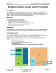
Introduction
This application note describes the 1080p60 camera image processing reference design that
showcases various features of the ZVIK, provides a working camera image processing
example design, and introduces several Xilinx video IP cores.
Video input is generated by the VITA-2000 image sensor from ON Semiconductor, which is
configured for 1080p60 resolution. The raw Bayer sub-sampled image is converted to an RGB
image by an image processing pipeline implemented using LogiCORE™ IP video cores that
remove defective pixels, de-mosaic, and color-correct the image. A video frame buffer is
implemented in the processing system (PS) DDR3 memory, making images accessible to the
ARM® processor cores via the AXI Video Direct Memory Access (VDMA). The video frame
buffer is not required for the operation of the image processing pipeline, but is included in the
design to enable the capture of input video images for analysis. Figure 1 shows a block diagram
of the design.
© Copyright 2013 Xilinx, Inc. Xilinx, the Xilinx logo, Artix, ISE, Kintex, Spartan, Virtex, Vivado, Zynq, and other designated brands included herein are trademarks of Xilinx in the
United States and other countries. ARM, AMBA, and CoreSight are trademarks of ARM in the EU and other countries. HDMI and High-Definition Multimedia Interface are
trademarks of HDMI Licensing LLC. MATLAB is a registered trademark of The MathWorks, Inc. All other trademarks are the property of their respective owners.
XAPP794 (v1.2) January 2, 2013
www.xilinx.com
1
Introduction
X-Ref Target - Figure 1
DDR3
Processing
System
Firmware
on SD Card
DDR Memory Controller
S_AXI4_HPx
M_AXI4_GP
AXI4 Stream
AMBA® Switches
Hardened
Peripherals
(USB, GigE,
CAN, SPI,
UART, 12C
GPIO)
PC running
Web-based GUI
APU
Dual Core
Cortex-A9 + OCM
AMBA Switches
Camera
Input
Image
Processing
Pipeline
AXI
VDMA
VITA-2000
Camera
HDMI
Output
Programmable Logic
HDMI Monitor
X794_01_102512
Figure 1:
1080p60 Camera Design Block Diagram
A web-based graphical user interface (GUI) allows configuring each of the Xilinx video IP cores
in the image processing pipeline, displaying information about the incoming image such as
histograms of the data, and enables processor-based operations on the data such as automatic
white balance and automatic exposure.
The hardware evaluation cores contained in the design time out after approximately four hours,
resulting in a blank screen. At this point, the board must be power-cycled to reload the design.
XAPP794 (v1.2) January 2, 2013
www.xilinx.com
2
Introduction
Host PC System Requirements
The host PC requirements to operate the camera design and its applications are:
•
32-bit/64-bit host PC with Ethernet port running Windows XP or Windows 7 Professional
32-bit/64-bit, or Ubuntu 10 or later 32-bit/64-bit Linux distribution.
•
UART connected terminal (for example, Tera Term 4.69 or HyperTerminal).
•
Zip/Unzip software (for example, 7-Zip).
•
Web browser such as Internet Explorer (to operate the web-based GUI).
•
USB-UART driver from Silicon Labs [Ref 39] (might already be installed). For information
about installing the USB-UART driver, see Zynq-7000 All Programmable SoC: ZC702
Evaluation Kit and Video and Imaging Kit Getting Started Guide [Ref 1].
To build the hardware and software components, the ISE® Design Suite: Embedded Edition
14.2 with compatible OS is also required.
Target Hardware Requirements
The target hardware requirements for running the camera design and its applications are:
•
Zynq-7000 All Programmable SoC Video and Imaging Kit, including:
•
Xilinx XC7Z020 CLG484-1 SoC-based ZC702 evaluation board.
•
Avnet FMC-IMAGEON FMC module.
•
VITA-2000 camera module (including optics, tripod, and cable).
•
HDMI cable.
•
SD-MMC flash card.
•
12V power supply.
•
HDMI monitor supporting 1080p60 resolution. A DVI monitor can also be used, but an
HDMI female to DVI-D male connector adapter must be obtained (not provided with the
kit). The connector adapter is available at most electronic retailers or through a variety of
online sources.
•
SD-MMC flash card writer.
For more information on the Zynq-7000 AP SoC Video and Imaging Kit, refer to:
www.xilinx.com/zvik
For more information on the Zynq-7000 AP SoC ZC702 evaluation board (including hardware
user manual, schematics, and BOM), refer to:
www.xilinx.com/zc702
For more information on the Avnet FMC-IMAGEON FMC Module with ON Semiconductor
image sensor, refer to:
http://www.em.avnet.com/fmc-imageon-v2000c
XAPP794 (v1.2) January 2, 2013
www.xilinx.com
3
Running the Demonstration
Running the
Demonstration
This section describes how to run the 1080p60 camera image processing reference design on
the ZVIK.
Reference Design File
The reference design files for this application note can be downloaded from:
https://secure.xilinx.com/webreg/clickthrough.do?cid=199792
Table 1 shows the reference design matrix.
Table 1: Reference Design Matrix
Parameter
Description
General
Developer name
Xilinx
Target devices
Zynq-7000 AP SoC
Source code provided
Yes
Source code format
VHDL (some sources encrypted)
IP used
EDK and CORE Generator Video IP Cores
Simulation
Functional simulation performed
N/A
Timing simulation performed
N/A
Test bench used for functional and timing
simulations
N/A
Test bench format
N/A
Simulator software/version used
N/A
SPICE/IBIS simulations
N/A
Implementation
Synthesis software tools/version used
XST 14.2
Implementation software tools/version used
ISE® Design Suite 14.2: System Edition
Static timing analysis performed
Yes (pass timing in PAR/TRACE)
Hardware Verification
Hardware verified
Yes
Hardware platform used for verification
Zynq-7000 Video and Imaging Kit
Installing Design Files
Download the ZVIK_Camera_Design_14_2 files to the C: drive of the host PC:
C:\zvik_camera
Note: If another location is chosen, there should be no spaces in the folder names.
XAPP794 (v1.2) January 2, 2013
www.xilinx.com
4
Running the Demonstration
Preparing the SD Card
Pre-built binaries for the camera design are provided in this directory:
..\zvik_camera\binaries\sd_content
Create a backup copy of the files on the SD card provided with the kit to enable them to be
restored if desired. These files are also available on the ZVIK product page. Copy the contents
of the sd_content directory to the root directory of the SD card.
By default, the design configures the ZVIK for IP address 192.168.1.10. This requires
configuring the host computer to a compatible IP address, such as 192.168.1.20. If this is not
possible, the IP address of the ZVIK in the configuration script should be changed:
..\zvik_camera\binaries\sd_content\config_my_ip.sh
On a Windows host, use a text editor that does not alter the end of line characters, such as
Notepad.
X-Ref Target - Figure 2
X794_02_111512
Figure 2:
Modifying the ZVIK IP Address
With a subnet mask of 255.255.255.0, the first three number groups of the IP address must be
identical in both the host computer IP address and the ZVIK IP address. For example, if the
ZVIK is configured with the IP address 192.168.1.10 (and subnet mask 255.255.255.0), the
host must be configured with an IP address containing identical numbers in the first three
positions and a differing number in the fourth group, such as 192.168.1.20.
Configuring the Host IP Address
Configure the IP address of the host computer to one that is compatible with the ZVIK IP
address discussed in Preparing the SD Card. Record the host PC's original network settings so
they can be restored after running the demonstration. Configure the computer’s IP address to
192.168.1.20 (or similar). The subnet mask can be 255.255.255.0. The screen captures and
icon names shown below might be slightly different depending on the computer’s operating
system version.
For Windows 7:
1. Click the Start button and select Control Panel.
2. Select Network and Sharing Center.
3. Select Change Adapter Settings from the options on the left panel.
4. Right click the adapter corresponding to the wired Ethernet port identified as a local area
connection and select Properties.
5. Accept the User Account Control dialog box by selecting Yes.
6. Click the Internet Protocol Version 4 (TCP/IPv4) entry and select Properties.
7. On the General tab, select the radio button for Use the following IP address.
8. In the IP address: field, enter 192.168.1.20 or a value that is compatible with the ZVIK IP
address configured in the previous section.
XAPP794 (v1.2) January 2, 2013
www.xilinx.com
5
Running the Demonstration
9. Click the Subnet mask: field and ensure that it is populated with 255.255.255.0. The dialog
box should appear be similar to Figure 3.
X-Ref Target - Figure 3
X794_03_102512
Figure 3:
Host Computer IP Address Configuration Dialog Box
10. Select OK to close the Internet Protocol Version 4 (TCP/IPv4) dialog box. Select OK to
close the Local Area Connection Properties dialog box.
Assembling the Camera
If the camera assembly has been completed, go to Setting Up the Hardware.
The ZVIK package contains these components, which must be assembled:
1. IR cut filter
2. Lens (2/3”, 8 mm)
3. VITA-2000-C image sensor module (with C-mount lens holder)
4. Tripod
5. LCEDI cable
6. FMC-IMAGEON FMC module
XAPP794 (v1.2) January 2, 2013
www.xilinx.com
6
Running the Demonstration
To assemble the camera:
1. Remove both protective caps from the lens (2) (Figure 4).
X-Ref Target - Figure 4
5
4
2
6
3
1
X794_04_102612
Figure 4:
VITA-2000 Camera Assembly Step 1
2. Attach the IR cut filter (1) to the lens (2) (Figure 5). The filter screws onto the front of the
lens.
X-Ref Target - Figure 5
4
5
3
6
X794_05_102612
Figure 5:
XAPP794 (v1.2) January 2, 2013
VITA-2000 Camera Assembly Step 2
www.xilinx.com
7
Running the Demonstration
3. Screw the IR cut filter and lens assembly onto the VITA-2000 image sensor module (3)
(Figure 6). The image sensor module has a lens holder with an opening for standard
C-mount lenses.
X-Ref Target - Figure 6
4
5
6
X794_06_102612
Figure 6:
VITA-2000 Camera Assembly Step 3
4. Attach the tripod (4) to the bottom of the VITA-2000 image sensor module (Figure 7). The
image sensor module lens holder has a hole that accepts standard tripods having a 1/4
inch screw with 20 threads per inch.
X-Ref Target - Figure 7
5
6
X794_07_102612
Figure 7:
XAPP794 (v1.2) January 2, 2013
VITA-2000 Camera Assembly Step 4
www.xilinx.com
8
Running the Demonstration
5. Attach the LCEDI cable (5) to the back of the VITA-2000 image sensor module (Figure 8).
Both ends of the LCEDI are identical. Either end can be connected to the image sensor
module.
X-Ref Target - Figure 8
6
X794_08_102612
Figure 8: VITA-2000 Camera Assembly Step 5
6. Attach the other end of the LCEDI cable to the FMC-IMAGEON FMC module (6) (Figure 9).
X-Ref Target - Figure 9
X794_09_102612
Figure 9: VITA-2000 Camera Assembly Step 6
The VITA-2000 color camera assembly is complete.
XAPP794 (v1.2) January 2, 2013
www.xilinx.com
9
Running the Demonstration
7. The IMAGEON FMC Module connects to the FMC2 connector of the ZC702 board FMC
carrier. The flexibility of the LCEDI cable allows the camera to be positioned in virtually any
direction (Figure 10).
X-Ref Target - Figure 10
X794_10_102612
Figure 10:
XAPP794 (v1.2) January 2, 2013
VITA-2000 Camera Assembly Step 7
www.xilinx.com
10
Running the Demonstration
8. The ZVIK package also contains two standoffs and four screws that secure the IMAGEON
FMC module to the ZC702 board. The package also contains four longer screws, standoffs,
and rubber feet to support the free end of the board. Assemble the hardware, as shown in
Figure 11.
X-Ref Target - Figure 11
X794_11_102612
Figure 11:
VITA-2000 Camera Assembly Step 8
Setting Up the Hardware
Figure 12 illustrates how to connect the ZVIK for the 1080p60 camera design.
X-Ref Target - Figure 12
Avnet
FMC Adapter
VITA-2000 Camera
Firmware
on SD Card
Xilinx ZC702 Board
HDMI
OUT
USB-Serial
Ethernet
1080P60 HDMI Monitor
Web-based GUI
X794_12_103112
Figure 12:
XAPP794 (v1.2) January 2, 2013
1080p60 Camera Design Hardware Setup
www.xilinx.com
11
Running the Demonstration
Connect the ZVIK hardware as follows:
1. Position the Avnet FMC-IMAGEON board on FMC slot #2 of the ZC702 board.
2. Connect the VITA-2000 camera to the FMC module with the provided LCEDI cable.
3. Connect the HDMI monitor to the ZC702 HDMI out connector (P1) with the provided HDMI
cable. If a DVI monitor is used, an HDMI female to DVI-D male connector adapter must be
provided. The connector adapter is available at most electronic retailers or through online
sources.
4. Connect the USB-Serial port on the ZC702 board (J17 labeled USB UART) to the host
computer using the provided USB Mini-B to USB-A cable.
5. Connect the Gbit Ethernet connector on the ZC702 to the host computer using the
provided Ethernet cable.
6. Ensure that the power switch on the ZC702 board is off by moving the switch away from the
power connector.
7. Connect the 12V power supply to the ZC702 board.
8. Insert the SD card into the ZC702 board SD card connector.
9. Ensure that the switches are set as shown in Figure 13, allowing the ZC702 board to boot
from the SD-MMC card.
X-Ref Target - Figure 13
X794_13_102612
Figure 13: Switch Settings for the SD-MMC Card Boot Mode Switch
10. Ensure that the monitor is set for HDMI (or DVI if using an HDMI female to DVI-D male
adapter) at 1920 x 1080 resolution.
11. Power on the ZC702 board.
Observing the Linux Console on the Serial Port
During boot, the Zynq-7000 SoC displays these steps on its serial port:
•
First stage boot loader (FSBL) output
•
U-Boot output
•
Linux console output
XAPP794 (v1.2) January 2, 2013
www.xilinx.com
12
Running the Demonstration
To view this serial output, open a terminal window using the UART connection program (Terra
Term or Hyperterminal) with these settings:
•
115200 baud
•
8 data bits
•
No parity
•
1 stop bit
•
No flow control
To determine which host computer COM port is mapped to the ZC702 Silicon Labs driver,
follow these steps (for Windows):
Note: If not already installed, refer to the Zynq-7000 All Programmable SoC: ZC702 Evaluation Kit and
Video and Imaging Kit Getting Started Guide [Ref 1].
1. Right-click My Computer and select Properties.
2. Select the Hardware tab.
3. Click Device Manager.
4. Expand the Ports (COM & LPT) section.
5. Make note of the COM port for the Silicon Labs CP210x USB to UART Bridge item. This is
the COM port that must be selected in the serial terminal program (Figure 14).
X-Ref Target - Figure 14
X794_14_102612
Figure 14:
Determining COM Port in Windows
In the example illustrated in Figure 14, the COM port is COM4. This can be different for each
computer.
XAPP794 (v1.2) January 2, 2013
www.xilinx.com
13
Running the Demonstration
To restart the boot process, press the POR_B button (SW1) located close to the SD card
connector or power cycle the ZC702 board.
This boot sequence should be observed:
1. The ZC702 board is powered on.
2. The DONE LED is off.
3. The first stage bootloader takes approximately 20 seconds.
4. Camera design hardware is loaded into programmable logic.
5. The DONE LED turns on.
6. U-Boot takes approximately 30 seconds.
7. Linux Kernel boot takes approximately 15 seconds.
8. Camera design software is executed (this takes approximately 5 seconds).
The total boot sequence should take approximately 70 seconds (just over one minute).
U-Boot generates this output on the serial console:
U-Boot 2010.09-01918-g068cc03 (Jan 20 2012 - 14:02:15)
Xilinx Pele Emulation Platform
DRAM: 256 MiB
## Unknown FLASH on Bank 1 - Size = 0x00000000 = 0 MB
Flash: 0 Bytes
MMC:
SDHCI: 0
Using default environment
In:
serial
Out:
serial
Err:
serial
Hit any key to stop autoboot: 0
Copying Linux from SD to RAM...
.
.
.
++ Mounting SD card to /mnt
++ Configuring IP Address
GEM: lp->tx_bd ffdfb000 lp->tx_bd_dma 2f220000 lp->tx_skb ee17d580
GEM: lp->rx_bd ffdfc000 lp->rx_bd_dma 2e47f000 lp->rx_skb ee17d680
GEM: MAC 0xefcb686e, 0x0000fb1d, 6e:68:cb:ef:1d:fb
GEM: phydev ef28ca00, phydev->phy_id 0x1410e40, phydev->addr 0x7
eth0, phy_addr 0x7, phy_id 0x01410e40
eth0, attach [Marvell 88E1116R] phy driver
++ Starting telnet daemon
++ Starting http daemon
++ Starting ftp daemon
++ Starting dropbear (ssh) daemon
rcS Complete
XAPP794 (v1.2) January 2, 2013
www.xilinx.com
14
Running the Demonstration
Finally, the camera demonstration software generates this output on the serial console:
------------------------------------------------------Xilinx Zynq-7000 AP SoC Video and Imaging Kit
--1080P60 Real-Time Camera Demonstration
------------------------------------------------------FMC-IPMI Initialization ...
Configure ZC702 IIC Mux for Port 6 (FMC2) ...
FMC Module Validation
Board Information:
Manufacturer
= Avnet
Product Name
= FMC-IMAGEON
Serial Number
= 6122
Part Number
= AES-FMCIMAGEON-G
SUCCESS : Detected FMC-IMAGEON module!
FMC-IMAGEON Initialization ...
FMC-IMAGEON Video Clock Initialization ...
Initialize Video Output for 1080P60 ...
Video Resolution = 1080P
Configure ZC702 IIC Mux for Port 1 (HDMI) ...
ZC702 HDMI Output Initialization ...
FMC-IMAGEON VITA Receiver Initialization ...
FMC-IMAGEON VITA Initialization ...
FMC-IMAGEON VITA Configuration for 1080P60 timing ...
VITA Status =
Image Width = 1920
Image Height = 1080
Frame Rate
= 61 frames/sec
Video Detector Initialization ...
Video Detector Configuration ...
Image Processing Pipeline (iPIPE) Initialization ...
Initializing iPipe cores ...
CCM done
Gamma done
CFA done
Stats done
Noise done
Enhance done
Initializing iPipe cores ... done!
Configure ZC702 IIC Mux for Port 1 (HDMI) ...
ZC702 HDMI Output Initialization ...
web avnet console : IN(/tmp/zvik_camera_linux_pipe_req) OUT(/tmp/zvik_camera_linux_pipe_rsp)
access(PIPE_IN_NAME, F_OK) ...done
access(PIPE_OUT_NAME, F_OK) ...done
open(PIPE_IN_NAME, O_RDONLY | O_NONBLOCK ) ...done
[web_session_handler] ... started
XAPP794 (v1.2) January 2, 2013
www.xilinx.com
15
Running the Demonstration
------------------------------------------------------Xilinx Zynq-7000 AP SoC Video and Imaging Kit
--1080P60 Real-Time Camera Demonstration
------------------------------------------------------General Commands:
help
Print the Top-Level menu Help Screen
quit
Exit console (if applicable)
verbose
Toggle verbosity on/off
delay
Wait for specified delay
mem
Memory accesses
I2C Commands
iic0
IIC accesses on FMC-IPMI I2C chain
iic1
IIC accesses on FMC-IMAGEON I2C chain
VITA Commands
vita
VITA commands (init, status, ...)
vspi
SPI accesses to VITA sensor
vreg
Memory accesses to VITA receiver
again
Analog gain (0-10)
dgain
Digital gain (0-4095) where 128 corresponds to 1.00
exposure
Exposure time (1-99) in percentage of frame period (16.66 msec)
iPIPE Commands
dpc
Defect Pixel Correction configuration
cfa
Color Filter Array Interpolation configuration
stats|s
Image Statistics
awb
Auto White Balance (on|off)
agc
Auto Gain Control (on|off)
aec
Auto Exposure Control (on|off)
geq
Gamma Equalization (on|off)
noise
Noise Reduction configuration
enhance
Image Enhance configuration
ccm
Color Correction Matrix configuration
gamma
Gamma Correction configuration
Video Source Selection
video
Video Source Initialization and Selection (vita, ipipe)
Video Frame Buffer Commands
vdma
Control frame buffer (start/stop/fill)
rec
Save frame buffer image to BMP file
play
Fill frame buffer image from BMP file
-----------------------------------------------------zvik_camera>
XAPP794 (v1.2) January 2, 2013
www.xilinx.com
16
Running the Demonstration
Adjusting the Lens
The content captured by the image sensor and processed by the image processing pipeline
should be visible on the monitor. If the image is blurry, adjust the lens focus, which ranges from
1 cm to 150 cm. If the image is too dark or too light, adjust the aperture (Figure 15). If the image
is black, the aperture should be adjusted to allow more light to enter the image sensor.
X-Ref Target - Figure 159
Focus
Aperture
X794_15_102612
Figure 15:
Adjusting the Focus and Aperture
To adjust the focus, aperture, or both:
1. Unlock the set screws by loosening them on both the aperture and focus ring.
2. Twist until the desired result is achieved.
3. Lock the setting by tightening the set screw.
This kit includes an 8 mm lens that is appropriate for a broad range of video applications. If this
lens is incorrect for a specific application, determine the required field of view (FOV) using
these measurements:
•
Distance to object (L)
•
Size of object (H x V)
XAPP794 (v1.2) January 2, 2013
www.xilinx.com
17
Running the Demonstration
The FOV measurements are shown in Figure 16.
X-Ref Target - Figure 16
H
Field
of
View
V
L
X794_16_102612
Figure 16: Determining the Required Field of View (FOV)
A lens calculator (such as http://www.1stvision.com/lens/lens_calculator.htm) can determine
the FOV and, consequently, the ideal lens choice for a specific application.
Using the Text-based Console
The Linux camera demonstration application accepts commands from a text-based console.
Type the help command to list the supported commands. The Linux application also has a
web-based GUI that significantly improves the ease-of-use and is described in Using the
Web-based GUI.
zvik_camera>help
------------------------------------------------------Xilinx Zynq-7000 AP SoC Video and Imaging Kit
--1080P60 Real-Time Camera Demonstration
------------------------------------------------------General Commands:
help
Print the Top-Level menu Help Screen
quit
Exit console (if applicable)
verbose
Toggle verbosity on/off
delay
Wait for specified delay
mem
Memory accesses
I2C Commands
iic0
IIC accesses on FMC-IPMI I2C chain
iic1
IIC accesses on FMC-IMAGEON I2C chain
VITA Commands
vita
VITA commands (init, status, ...)
vspi
SPI accesses to VITA sensor
vreg
Memory accesses to VITA receiver
trig
Trigger configuration (off/stress/internal/external/manual)
iPIPE Commands
dpc
Defect Pixel Correction configuration
cfa
Color Filter Array Interpolation configuration
stats|s
Image Statistics
awb
Auto White Balance (on|off)
agc
Auto Gain Control (on|off)
XAPP794 (v1.2) January 2, 2013
www.xilinx.com
18
Running the Demonstration
aec
Auto Exposure Control (on|off)
geq
Gamma Equalization (on|off)
irq|i
Image Statistics Interrupt (manual)
noise
Noise Reduction configuration
enhance
Image Enhance configuration
ccm
Color Correction Matrix configuration
gamma
Gamma Correction configuration
Video Source Selection
video
Video Initialization (hdmi, hdmii, hdmio, vita)
Record/Playback Commands
rec
Save frame buffer image to BMP file
play
Fill frame buffer image from BMP file
-----------------------------------------------------zvik_camera>
Type the {command} help command to obtain detailed help for a specific command. For
example, to save an image from the video frame buffer to the SD card (/mnt), type these
commands:
zvik_camera>rec help
rec help
Syntax :
rec {filename} => Write frame buffer image to BMP file
zvik_camera>rec /mnt/mypicture.bmp
rec /mnt/mypicture.bmp
height = 1080, width = 1920, n = 6220800
zvik_camera>
XAPP794 (v1.2) January 2, 2013
www.xilinx.com
19
Running the Demonstration
Using the Web-based GUI
To access the web-based GUI, open a web browser such as Internet Explorer and enter the
ZVIK IP address http://192.168.1.10 (or the address assigned in Preparing the SD Card). The
web page shown in Figure 17 appears.
X-Ref Target - Figure 17
X794_17_102612
Figure 17:
1080p60 Camera Design Web-based GUI
If the host computer cannot establish a connection, it might be necessary to disable virus
scanning, the firewall, or both. This is not typically required. To test whether the computer can
communicate over the Ethernet connection, open a Command Prompt window (this is done in
Windows 7 by selecting Start Button > All Programs > Accessories > Command Prompt)
and type ping 192.168.1.10 or ping followed by the IP address assigned to the ZVIK in the
previous section. If this is not successful, review the IP configurations set in Preparing the SD
Card and Configuring the Host IP Address.
XAPP794 (v1.2) January 2, 2013
www.xilinx.com
20
Running the Demonstration
Adjusting the Image Sensor Gain and Exposure
The image sensor gain and exposure can be adjusted using the controls shown in Figure 18.
X-Ref Target - Figure 18
X794_18_102612
Figure 18:
Image Sensor Gain and Exposure Controls
The check boxes shown in Figure 18 allow the gain and exposure to be adjusted automatically
by either of these two methods:
•
Processor Control: One of the Zynq-7000 SoC processors collects information about the
image from the Image Statistics IP core and uses this information to adjust the image
sensor exposure and gain settings. The Target Intensity slider allows the user to select the
desired target intensity.
•
Image Sensor Auto Gain/Exposure: Uses the image sensor internal auto gain/exposure
control (AEC) to control the gain and exposure. The Target Intensity slider allows the user
to select the desired target intensity.
Note: When the processor control boxes are checked, they disable both the manual gain and exposure
settings and the image sensor AEC.
Sliders allow the gain and exposure to be adjusted manually when the auto gain and exposure
check boxes are not selected.
XAPP794 (v1.2) January 2, 2013
www.xilinx.com
21
Running the Demonstration
The analog gain provides a course manual adjustment of the image sensor gain, as shown in
Table 2.
Table 2: Analog Gain Slider Settings
Setting
Description
0
Analog gain = 0.00
1
Analog gain = 1.14
2
Analog gain = 1.33
3
Analog gain = 1.60
4
Analog gain = 2.00
5
Analog gain = 2.29
6
Analog gain = 2.67
7
Analog gain = 3.20
8
Analog gain = 4.00
9
Analog gain = 5.33
10
Analog gain = 8.00
The digital gain slider provides a fine manual adjustment of the image sensor gain, as shown in
Table 3.
Table 3: Digital Gain Slider Settings
Setting
0.00–31.99
Description
Digital gain = 0.00–31.99
The exposure slider provides a manual adjustment of the image sensor exposure time, as
shown in Table 4.
Table 4: Exposure Slider Settings
Setting
1 – 99
XAPP794 (v1.2) January 2, 2013
Description
Exposure in percentage of frame time (16.6 ms):
1% = 0.16 ms
99% = 16.5 ms
www.xilinx.com
22
Running the Demonstration
Capturing a 1080P Image
The Image Capture section of the web-based GUI allows capturing an image from the video
frame buffer, as shown in Figure 19.
X-Ref Target - Figure 19
X794_19_102612
Figure 19:
Image Capture Controls
After clicking the Click to Take Snapshot button, a scaled-down version of the image is
displayed in the GUI. A full-size version of the image (24-bit RGB 1920 x 1080 bitmap (BMP))
can be saved to the host hard drive by right-clicking the image and selecting Save Picture As.
This allows analysis of the image with a separate image viewing program.
Configuring the Defective Pixel Correction
The Xilinx Defective Pixel Correction IP core can be configured with three sliders, as shown in
Figure 20.
X-Ref Target - Figure 20
X794_20_102612
Figure 20:
Defective Pixel Correction IP Core Controls
To observe the operation of the Defective Pixel Correction core, move the Pixel Age slider to
100. A few small white dots appear on the monitor. To better see the dots, point the image
sensor at a uniform dark background. These are defective pixels in the image sensor. As the
Pixel Age Slider is moved back to 0, the defective pixels are effectively removed from the image
by the Defective Pixel IP core processing.
XAPP794 (v1.2) January 2, 2013
www.xilinx.com
23
Running the Demonstration
Configuring the Color Filter Array Interpolation
The Xilinx Color Filter Array Interpolation IP core Bayer Phase setting (Figure 21) can be
changed, but only one setting produces a valid result with the VITA 2000 image sensor.
X-Ref Target - Figure 21
X794_21_102612
Figure 21:
Color Filter Array IP Core Control
Configuring the Spatial Noise Reduction
The Xilinx Image Noise Reduction IP core performs spatial noise reduction using a low-pass
filter that is edge adaptive. The Strength slider shown in Figure 22 allows the settings shown in
Table 5.
X-Ref Target - Figure 22
X794_22_102612
Figure 22:
Image Noise Reduction IP Core Control
Table 5: Spatial Noise Reduction Strength Settings
Setting
0
1–4
Description
Spatial Noise Reduction OFF.
Spatial Noise Reduction ON.
Number identifies strength of spatial noise reduction filter.
Configuring the Edge Enhancement
The Xilinx Image Edge Enhancement IP core performs edge detection and highlights the edges
in the color image. The Strength slider shown in Figure 23 allows the settings shown in Table 6.
The best image quality is usually achieved with a value of 1.
X-Ref Target - Figure 23
X794_23_102612
Figure 23:
Image Edge Enhancement IP Core Control
Table 6: Edge Enhancement Settings
Setting
Description
0
Edge Enhancement OFF
1-4
Edge Enhancement ON
Number identifies strength of edge enhancement
XAPP794 (v1.2) January 2, 2013
www.xilinx.com
24
Running the Demonstration
Configuring the Color Correction Matrix
The Xilinx Color Correction Matrix IP core provides color correction of the image to correct for
different illumination sources. The Color Correction IP core settings can be adjusted using the
GUI controls shown in Figure 24.
X-Ref Target - Figure 24
X794_24_102612
Figure 24:
Color Correction Matrix IP Core Controls
The white balance list box applies pre-determined color corrections for four illumination
conditions, as shown in Table 7.
Table 7: White Balance Settings
Setting
Description
Bypass
Color correction OFF (all coefficients are 1.0)
Daylight
Color correction ON for daylight lighting conditions
Cool White Fluorescent
Color correction ON for cool white fluorescent (4500°K) lighting
U30 (Hot Fluorescent)
Color correction ON for hot fluorescent (3000°K) lighting
Incandescent
Color correction ON for incandescent lighting
Alternatively, the white balance setting can be automatically controlled by one of the Zynq-7000
SoC processors. Based on the information received from the Image Statistics IP core, the
processor can select a weighted sum of one or more of the white balance configurations, based
on the calculated probability of each of the possible light sources.
The Brightness and Contrast sliders can be used to change the intensity of the image, making
it darker or brighter.
The Saturation slider can be used to change the intensity of the colors. A Saturation of 0
produces a grayscale image.
The color correction coefficients for the four illumination sources were generated by placing an
X-Rite ColorChecker 24 Patch Classic target [Ref 40] in an X-Rite Macbeth Judge II light booth
[Ref 41]. Bitmap images were collected using the GUI for the four different illumination settings
(Daylight, Cool White Fluorescent, U30, and Incandescent sources) with the color correction
matrix set to Bypass (no color corrections applied). Average values for the 24 patches at each
illumination setting were calculated by a MATLAB® software script. A second script is used to
model the Xilinx color correction matrix operations and determine a set of coefficients that
result in output from the color correction matrix that best matches the known target values for
the 24 patches. The MATLAB software scripts used to develop the coefficients for the Color
Correction Matrix IP core are included in the 1080p60 camera image processing design files
that can be downloaded from the ZVIK product page on Xilinx.com. Select the Docs and
Designs tab and look for the ZVIK_Camera_Design_14_2.zip download. Additional
XAPP794 (v1.2) January 2, 2013
www.xilinx.com
25
Running the Demonstration
information on development of the color correction coefficients can be found in an article titled
Image Sensor Color Calibration Using the Zynq-7000 SoC in the Xcell Journal [Ref 2].
Figure 25 illustrates the effects of white balance on the 24-patch ColorChecker chart for the
four different illumination sources:
X-Ref Target - Figure 25
Daylight
Cold White Fluorescent
U30
Incandescent
Uncorrected
Uncorrected
Uncorrected
Uncorrected
Corrected
Corrected
Corrected
Corrected
X794_25_102812
Figure 25:
White Balance Color Checker Results
The top four images show the output of the image sensor and image processing pipeline with
no color correction applied for four different illumination sources. There are marked differences
in color for all four cases. The bottom images show the output with the various color corrections
applied for each different illumination source and illustrate how the white balance setting
corrects the colors. These images were taken in the X-Rite Macbeth Judge II light booth using
the ZVIK camera design.
Xilinx provides support for the 1080p60 camera image processing reference design, IP cores
such as the Color Correction Matrix, and Xilinx FPGA and SoC products. Xilinx cannot provide
assistance to customers developing color correction coefficients for the ON Semiconductor or
any other image sensor. Development of custom color correction coefficients is the
responsibility of the customer. The MATLAB software scripts are provided as examples to
assist customers in developing their own color corrections for different image sensors. Consult
the Additional Resources tab of the ZVIK product page for additional information.
XAPP794 (v1.2) January 2, 2013
www.xilinx.com
26
Running the Demonstration
Configuring the Gamma Correction
The gamma correction IP core is implemented as a look-up table that is applied to all three
color channels. The gamma correction IP core can be adjusted using the GUI controls shown
in Figure 26.
X-Ref Target - Figure 26
X794_26_102612
Figure 26:
Gamma Correction IP Core Controls
The Gamma Table list box allows the manual gamma correction settings shown in Table 8.
Table 8: Gamma Table Setting
Setting
Description
Linear
Gamma Correction OFF (linear look-up table)
Compression Table 1/2.2
Gamma Correction ON (gamma = 1/2.2)
Compression Table 1/1.6
Gamma Correction ON (gamma = 1/1.6)
Expansion Table 1.6
Gamma Correction ON (gamma = 1/1.6)
Expansion Table 2.2
Gamma Correction ON (gamma = 1/2.2)
Alternatively, the gamma correction setting can be automatically controlled by one of the
Zynq-7000 SoC processors. Based on the information received from the image statistics IP
core, the processor can calculate a look-up table that makes the most efficient use of the 0–255
values based on the image intensity histogram. The strength slider allows the user to adjust the
gamma correction strength applied by the processor.
XAPP794 (v1.2) January 2, 2013
www.xilinx.com
27
Running the Demonstration
Understanding the Image Statistics
The Xilinx Image Statistics IP core provides hardware-based image analysis to support
auto-focus, auto-exposure, and auto-white balance applications. The third column in the
web-based GUI provides feedback from the image statistics IP core in the form of histograms,
as shown in Figure 27.
X-Ref Target - Figure 27
X794_27_121412
Figure 27: Histograms from the Xilinx Image Statistics IP Core
Four histograms are displayed. The content of each histogram is described by the color bar at
the bottom of each histogram. The intensity histogram has a gray color bar, the red channel
histogram has a red color bar, the green histogram has a green bar, and the blue histogram has
a blue bar.
XAPP794 (v1.2) January 2, 2013
www.xilinx.com
28
Running the Demonstration
The intensity histogram (Figure 28) provides information about the overall image exposure.
X-Ref Target - Figure 28
X794_28_121412
Figure 28:
Intensity Histogram
In addition to the histogram distribution of the data, the bar at the top of the histogram provides
visual feedback on the exposure:
•
A red bar on the top left indicates that the image is under-exposed according to the
formula:
(number of pixels in the 0–64 range) * (under-exposure threshold) > (number of pixels in
the 64–192 range)
•
A red bar on the top right indicates that the image is over-exposed according to the this
formula:
(number of pixels in the 192–255 range) * (over-exposure threshold) > (number of pixels in
the 64–192 range)
•
A green bar on the top indicates that the image has good exposure (neither
under-exposed or over-exposed)
The under- and over-exposure thresholds can be adjusted by moving the Under-Exp and
Over-Exp sliders at the top of the third column, as shown in Figure 29.
X-Ref Target - Figure 29
X794_29_102612
Figure 29:
XAPP794 (v1.2) January 2, 2013
Image Statistics Exposure Controls
www.xilinx.com
29
Running the Demonstration
The red histogram (Figure 30) shows the distribution of red pixel values.
X-Ref Target - Figure 30
X794_30_121412
Figure 30:
•
Red Histogram
A red bar on the top right indicates that the red color channel is over-saturated according
to the formula:
(number of pixels in the 242–255 range) > 0
•
A green bar on the top indicates that the red color channel is not over-saturated.
The green histogram (Figure 31) shows the distribution of green pixel values.
X-Ref Target - Figure 31
X794_31_121412
Figure 31:
•
Green Histogram
A red bar on the top right indicates that the green color channel is over-saturated
according to the formula:
(number of pixels in the 242–255 range) > 0
•
A green bar on the top indicates that the green color channel is not over-saturated.
The blue histogram (Figure 32) shows the distribution of blue pixel values.
X-Ref Target - Figure 32
X794_32_121412
Figure 32:
•
Blue Histogram
A red bar on the top right indicates that the blue color channel is over-saturated according
to the formula:
(number of pixels in the 242–255 range) > 0
XAPP794 (v1.2) January 2, 2013
www.xilinx.com
30
Hardware Platform
•
A green bar on the top indicates that the blue color channel is not over-saturated.
The contents of the histograms are static by default, unless configured otherwise. There are
two options for updating the histograms (see Figure 29):
1. To update the contents of the histograms a single time, click the Update button.
2. To periodically update the histograms, click the Click to Start button. To stop periodically
updating the histograms, click the Click to Stop button. The frequency of the update can
be adjusted by moving the Interval (msec) slider.
Hardware
Platform
The block diagram for the 1080p60 camera reference design is shown in Figure 33.
X-Ref Target - Figure 33
DDR3
S_AXI4_HPx
M_AXI4_GP
Processing
System
AXI4 Stream
DDR Memory Controller
AMBA Switches
Hardened
Peripherals
(USB, GigE,
CAN, SPI,
UART, 12C
GPIO)
APU
Dual Core
Cortex-A9 + OCM
AMBA Switches
AXI-Lite Interconnect
AXI
VDMA
VITA-2000
Camera In
VITA
Receiver
Image
Pipe
RGB to
YCbCr422
HDMI
Output
On-board
HDMI Out
X794_33_111912
Figure 33:
1080p Camera Hardware Block Diagram
The details of the image processing pipeline are shown in Figure 34.
X-Ref Target - Figure 34
AXI
VTC
AXI
DPC
AXI
CFA
RGB
YUV
AXI
Noise
AXI
Enhance
YUV
RGB
AXI
CCM
AXI
STATS
Figure 34:
XAPP794 (v1.2) January 2, 2013
AXI
Gamma
AXI
VTC
X794_34_102612
1080p Camera Image Processing Pipeline
www.xilinx.com
31
Hardware Platform
This design is implemented in a Zynq-7000 AP SoC device (XC7Z020CLG484-1) using the
ISE Design Suite: Embedded Edition 14.2. The PL hardware utilization for the implemented
design is shown in Table 9.
Table 9: Hardware Utilization
FPGA Components
Total Available
Used
% Used
I/Os
200
50
25
LUTs
53,200
29,708
55
Registers
106,400
36,255
34
DSP48s
220
54
24
RAMB36E1/FIFO36E1s
140
48
34
RAMB18E1/FIFO18E1s
280
26
9
Block RAM
A more detailed resource utilization summary can be found in this directory:
..\zvik_camera\doc\system_summary.html
Note: Device resource utilization results are dependent on the implementation tool versions. Exact
results can vary. These numbers should be used as a guideline.
There are many advantages to implementing this system in a Zynq-7000 AP SoC:
•
Processing-intensive pixel operations are efficiently implemented in the PL.
•
Complex decision-making algorithms like automatic white balance and automatic
exposure are efficiently implemented in the PS.
•
Processor operations can easily be modified or added to the PS.
•
The hardware system can easily be expanded or customized by adding/removing
instances of Xilinx IP cores from the Xilinx IP catalog or third-party sources.
•
The hardware system can be further customized by adding custom logic that either
interfaces to the PS or is totally independent.
•
A choice of Zynq-7000 AP SoC sizes allows room to shrink or expand the hardware PL to
meet system requirements.
System Features
Processing System
•
Two ARM Cortex™-A9 processors, each with a 32 KB instruction cache and a 32 KB data
cache, and a NEON coprocessor
•
ARM processors at 800 MHz
•
512 KB of level-2 cache
•
256 KB of on-chip RAM
•
128 KB of on-chip ROM
•
AMBA® AXI interconnect
•
Multi-protocol, 32-bit DDR DRAM controller
•
DDR3 DRAM at 533 MHz
•
Standard peripheral interfaces including flash, USB, Ethernet, UART, I2C, and more
•
High bandwidth interconnect to and from the PL
•
Power domain independent of the PL
XAPP794 (v1.2) January 2, 2013
www.xilinx.com
32
Hardware Platform
Programmable Logic
•
One 64-bit AXI interconnect at 150 MHz
•
Two 32-bit AXI interconnect at 75 MHz
•
VITA receiver (serial LVDS) interface
•
Image processing pipeline
•
Video frame buffer (AXI-VDMA)
•
HDMI output interface
Device Address Map
The pcores that are instantiated on the M_AXI_GP0 port are shown in Table 10.
Table 10: AXI GP0 Port Address Map
Instance
Peripheral
Base Address
High Address
axi_vdma_0
axi_vdma_v5_00_a
0x40090000
0x4009FFFF
IIC_MAIN
axi_iic_v1_01_a
0x40800000
0x4080FFFF
fmc_imageon_iic_0
axi_iic_v1_01_a
0x40900000
0x4090FFFF
fmc_imageon_vita_receiver_0
fmc_imageon_vita_receiver_v1_09_a
0x40820000
0x4082FFFF
axi_vtc_2
axi_vtc_v3_00_a
0x40440000
0x4044FFFF
xsvi_mux_0
xsvi_mux_v1_00_b
0x40600000
0x4060FFFF
xsvi_mux_1
xsvi_mux_v1_00_b
0x40610000
0x4061FFFF
vtc_0
axi_vtc_v3_00_a
0x7DE20000
0x7DE2FFFF
dpc_0
axi_dpc_v4_00_a
0x75000000
0x7500FFFF
cfa_0
axi_cfa_v4_00_a
0x64C00000
0x64C0FFFF
stats_0
axi_stats_v3_00_a
0x6CE00000
0x6CE0FFFF
noise_0
axi_noise_v3_00_a
0x76000000
0x7600FFFF
enhance_0
axi_enhance_v3_00_a
0x7B200000
0x7B20FFFF
ccm_0
axi_ccm_v3_00_a
0x64C20000
0x64C2FFFF
gamma_0
axi_gamma_v4_00_a
0x6FC00000
0x6FC0FFFF
vtc_1
axi_vtc_v3_00_a
0x7DE00000
0x7DE0FFFF
System Configuration
Clocking
The PL design has several clock domains: AXI MM (memory-mapped) interconnect, AXI
register interface, and video clock(s). These domains run at 150 MHz, 75 MHz, and
148.5 MHz, respectively.
The first clock generator module receives a 100 MHz input clock from PS FCLK0 and
generates 75 MHz and 150 MHz. The AXI4-Lite interconnect operates on the 75 MHz clock
domain.
The AXI MM interconnect to the HP port of the PS operates on the 150 MHz clock domain. The
stream to memory map (S2MM) and memory map to stream (MM2S) channels of the VDMA
operate on the 150 MHz clock domain.
XAPP794 (v1.2) January 2, 2013
www.xilinx.com
33
Hardware Platform
The video clock comes from the external clock synthesizer on the Avnet FMC-IMAGEON card.
The video input and output interfaces, as well as the video processing pipeline operate on the
video clock domain.
The clock signals are shown in Table 11.
Table 11: System Clocks
Clock Signal
Frequency
(MHz)
Source
Use
FPGA_CLK
PS – FPGA_CLK0
100
Input clock to clock generator.
clk_100mhz
Clock generator – MMCM (1)
100
Not used.
clk_200mhz
Clock generator – MMCM
200
200 MHz reference clock for deserializer in VITA
receiver.
clk_75mhz
Clock generator – MMCM
75
Slave clock for AXI4-Lite interconnect.
clk_150mhz
Clock generator – MMCM
150
Clock for AXI MM interconnect.
clk_25mhz
Clock generator – MMCM
25
Slowest sync clock, used for reset logic.
fmc_imageon_video_clk1
External video clock coming
from clock synthesizer on
FMC module
148.5
Input clock to clock generator.
vid_out_clk
Clock generator – MMCM
148.5
Clock for video input and video output interfaces
and video processing pipeline.
vita_clk_ref
Clock generator – MMCM
37.125
Reference clock for VITA image sensor.
Notes:
1.
Mixed-mode clock manager.
Reset
The proc_sys_reset module implements a reset scheme. Input to the proc_sys_reset core is
generated by PS FCLK_RESET0. The polarity of input reset to this block is indicated by the
parameter C_EXT_RESET_HIGH. In this design, C_EXT_RESET_HIGH is set to 0 because
the reset generated by the PS is active-Low. This block generates various types of resets, such
as reset for interconnect and peripheral reset. All the blocks in the PL are driven by interconnect
reset, which is active-Low.
For detailed information about the complete feature set and a functional description of the
proc_sys_reset IP core, refer to LogiCORE IP Processor System Reset Module Product
Specification [Ref 4].
AXI Interconnect
The PL design has one interconnect for the AXI memory-mapped master and one interconnect
for the AXI register interface.
The AXI memory-mapped interconnect is connected to a master, the AXI VDMA. It is also
connected to a slave, the HP0 port of the Zynq-7000 AP SoC PS. This interconnect operates at
150 MHz, and the data width is 64 bits. The read/write acceptance and issuance are set to 8.
The acceptance and issuance helps improve system performance. The PS HP port can accept
a maximum burst length of 16.
This read/write acceptance and issuance setting imposes a limitation on getting minimum
acceptable bandwidth for every master in a multi-master system. The optimum setting of
issuance and acceptance reduces throttle on the bus and compensates for long latencies.
The AXI register interface is clocked at 75 MHz. The Zynq-7000 AP SoC PS GP0 port acts as
the master on this interconnect and connected slaves have register maps. AXI TPG and AXI
VTC are examples of slaves connected to this interconnect. The operations of the video
XAPP794 (v1.2) January 2, 2013
www.xilinx.com
34
Hardware Platform
pipeline are controlled by registers inside every IP core. Depending upon the data flow required
in the video pipeline, the processor writes these registers through the AXI4-Lite interconnect.
The AXI4-Lite interconnect accepts write or read transfers from the processor, performs
address decoding, selects a particular slave, and establishes a communication channel
between the processor and the slave device.
For detailed information about the complete feature set and a functional description of the AXI
interconnect IP, refer to LogiCORE IP AXI Interconnect [Ref 5].
Video System Configuration
AXI VDMA
AXI VDMA has an AXI4-Stream interface on one side and an AXI memory-mapped interface on
the other side. The AXI VDMA has two channels: MM2S and S2MM. The MM2S channel is not
implemented in this design.
The S2MM channel receives data from the master device connected through the streaming
interface. The C_S_AXIS_S2MM_TDATA_WIDTH parameter decides the width of the
streaming interface. Data received on the streaming interface is then written into the system
memory through the memory-mapped interface. The C_M_AXI_S2MM_DATA_WIDTH
parameter decides the data width of the memory-mapped interface and
C_S2MM_MAX_BURST_LENGTH governs the burst length of the write transaction.
In this design, the stream interface data width is set to 32 bits and the memory-mapped
interface width is 64 bits. The AXI VDMA is used in simple register direct mode, which removes
the area cost of the scatter gather feature. Initialization, status, and management registers in
the AXI VDMA core are accessed through an AXI4-Lite slave interface. To get the best possible
throughput for AXI VDMA instances, the maximum burst length is set to 16. In addition, the
master interfaces have a read and write issuance of 8 and a read and write FIFO depth of 512
to maximize throughput. The line buffers inside the AXI VDMA for the read and write sides are
set to 4K deep, and the store and forward feature of the AXI VDMA are enabled on both
channels to improve system performance and reduce the risk of system throttling.
For additional information about the AXI VDMA LogiCORE solution and the detailed product
guide, refer to the AXI VDMA product page on Xilinx.com:
http://www.xilinx.com/products/intellectual-property/axi_video_dma.htm
Video Processing Pipeline Details
Video Timing Controller
The AXI Video Timing Controller (VTC) is a general-purpose video timing generator and
detector. The input side of this core automatically detects horizontal and vertical
synchronization pulses, polarity, blanking timing, and active video pixels. The output side of the
core generates the horizontal and vertical blanking and synchronization pulses. There are two
AXI VTC cores in the image processing pipeline, as shown in Figure 35.
X-Ref Target - Figure 35
AXI
VTC
AXI
DPC
AXI
CFA
RGB
YUV
AXI
Noise
AXI
Enhance
YUV
RGB
AXI
Stats
Figure 35:
AXI
CCM
AXI
Gamma
AXI
VTC
X794_35_102612
AXI VTC Core Pipeline Position
The first AXI VTC core detects the video resolution of the video input coming from the VITA
receiver. The second AXI VTC core is used to regenerate the VSYNC and HSYNC signals that
were not preserved by the image processing pipeline.
XAPP794 (v1.2) January 2, 2013
www.xilinx.com
35
Hardware Platform
For additional information about the Video Timing Controller LogiCORE solution and the
detailed product guide, refer to the Video Timing Controller product page on Xilinx.com:
http://www.xilinx.com/products/intellectual-property/EF-DI-VID-TIMING.htm
Defective Pixel Correction
The AXI Defective Pixel Correction (DPC) core is the first processing element in the image
processing pipeline, as shown in Figure 36.
X-Ref Target - Figure 36
AXI
VTC
AXI
DPC
AXI
CFA
RGB
YUV
AXI
Noise
AXI
Enhance
YUV
RGB
AXI
CCM
AXI
Gamma
AXI
Stats
Figure 36:
AXI
VTC
X794_36_102612
AXI DPC Core Pipeline Position
This core is responsible for correcting defective pixels, as illustrated in Figure 37.
X-Ref Target - Figure 37
X794_37_102612
Figure 37:
Defective Pixel Correction
For additional information about the Defective Pixel Correction LogiCORE solution and the
detailed product guide, refer to the Defective Pixel Correction product page on Xilinx.com:
http://www.xilinx.com/products/intellectual-property/EF-DI-DEF-PIX-CORR.htm
Color Filter Array Interpolation
The AXI Color Filter Array (CFA) core is the second processing element in the image
processing pipeline, as shown in Figure 38.
X-Ref Target - Figure 38
AXI
VTC
AXI
DPC
AXI
CFA
RGB
YUV
AXI
Noise
AXI
Enhance
YUV
RGB
AXI
Stats
Figure 38:
XAPP794 (v1.2) January 2, 2013
AXI
CCM
AXI
Gamma
AXI
VTC
X794_38_102612
AXI CFA Core Pipeline Position
www.xilinx.com
36
Hardware Platform
The most widespread and cost effective implementation of color image sensors involves
placing color filters on top of each pixel in a Bayer pattern arrangement, as shown in Figure 39.
.
X-Ref Target - Figure 39
X794_39_102612
Figure 39:
Bayer Pattern Color Filter
With this arrangement of color filters, each pixel captures only one of the three primary colors.
The CFA core restores the missing two colors based on neighboring pixels.
For additional information about the Color Filter Array Interpolation LogiCORE solution and the
detailed product guide, refer to the Color Filter Array Interpolation product page on Xilinx.com:
http://www.xilinx.com/products/intellectual-property/EF-DI-CFA.htm
Image Statistics Engine
The AXI STATS core is used to gather various image statistics from the image processing
pipeline (Figure 40) such as:
•
Intensity histograms
•
Color histograms
X-Ref Target - Figure 40
AXI
VTC
AXI
DPC
AXI
CFA
RGB
YUV
AXI
Noise
AXI
Enhance
YUV
RGB
AXI
CCM0
AXI
CCM1
AXI
Gamma
AXI
VTC
AXI
Stats
X794_40_102612
Figure 40:
AXI Stats Core Pipeline Position
For additional information about the Image Statistics Engine LogiCORE solution and the
detailed product guide, refer to the Image Statistics Engine product page on Xilinx.com:
http://www.xilinx.com/products/intellectual-property/EF-DI-IMG-STATS.htm
Color Space Conversion
The color space conversion cores are used in the image processing pipeline to convert to/from
the RGB color space and the YCrCb color space, as shown in Figure 41.
X-Ref Target - Figure 41
AXI
VTC
AXI
DPC
AXI
CFA
RGB
YUV
AXI
Noise
AXI
Enhance
YUV
RGB
AXI
CCM
AXI
Stats
Figure 41:
XAPP794 (v1.2) January 2, 2013
AXI
Gamma
AXI
VTC
X794_41_102612
Color Space Conversion Cores Pipeline Position
www.xilinx.com
37
Hardware Platform
For additional information about the Color Space Conversion LogiCORE solutions and the
detailed product guides, refer to the Color Space Conversion product pages on Xilinx.com:
http://www.xilinx.com/products/intellectual-property/RGB_to_YCrCb.htm
http://www.xilinx.com/products/intellectual-property/YCrCb_to_RGB.htm
Image Noise Reduction
The AXI NOISE core is used to remove spatial noise in the image processing pipeline, as
shown in Figure 42.
X-Ref Target - Figure 42
AXI
VTC
AXI
DPC
AXI
CFA
RGB
YUV
AXI
Noise
AXI
Enhance
YUV
RGB
AXI
CCM
AXI
Gamma
AXI
Stats
AXI
VTC
X794_42_100912
Figure 42: AXI Noise Core Pipeline Position
For additional information about the Image Noise Reduction LogiCORE solution and the
detailed product guide, refer to the Image Noise Reduction product page on Xilinx.com:
http://www.xilinx.com/products/intellectual-property/EF-DI-IMG-NOISE.htm
Image Edge Enhancement
The AXI ENHANCE core is used to accentuate edges in the image and is positioned in the
image processing pipeline, as shown in Figure 43.
X-Ref Target - Figure 43
AXI
VTC
AXI
DPC
AXI
CFA
RGB
YUV
AXI
Noise
AXI
Enhance
YUV
RGB
AXI
CCM0
AXI
CCM1
AXI
Gamma
AXI
Stats
AXI
VTC
X794_43_102612
Figure 43:
AXI Enhance Core Pipeline Position
For additional information about the Image Edge Enhancement LogiCORE solution and the
detailed product guide, refer to the Image Edge Enhancement product page on Xilinx.com:
http://www.xilinx.com/products/intellectual-property/EF-DI-IMG-ENHANCE.htm
Color Correction Matrix
The AXI Color Correction Matrix (CCM) core is used to implement various color corrections in
the image processing pipeline (Figure 44):
•
White balance
•
Brightness
•
Contrast
•
Saturation
X-Ref Target - Figure 44
AXI
VTC
AXI
DPC
AXI
CFA
RGB
YUV
AXI
Noise
AXI
Enhance
YUV
RGB
AXI
Stats
Figure 44:
XAPP794 (v1.2) January 2, 2013
AXI
CCM
AXI
Gamma
AXI
VTC
X794_44_102612
AXI CCM Core Pipeline Position
www.xilinx.com
38
Software Platform
For additional information about the Color Correction Matrix LogiCORE solution and the
detailed product guide, refer to the Image Edge Enhancement product page on Xilinx.com:
http://www.xilinx.com/products/intellectual-property/EF-DI-CCM.htm
Gamma Correction
The AXI GAMMA core implements look-up tables that are used to implement gamma
correction in the image processing pipeline, as shown in Figure 45.
X-Ref Target - Figure 45
AXI
VTC
AXI
DPC
AXI
CFA
RGB
YUV
AXI
Noise
AXI
Enhance
YUV
RGB
AXI
CCM
AXI
Gamma
AXI
Stats
Figure 45:
AXI
VTC
X794_45_102612
AXI Gamma Core Pipeline Position
For additional information about the Gamma Correction LogiCORE solution and the detailed
product guide, refer to the Gamma Correction product page on Xilinx.com:
http://www.xilinx.com/products/intellectual-property/EF-DI-GAMMA.htm
Software
Platform
An application to demonstrate the capabilities of the Zynq-7000 AP SoC PS and PL
combination for mainstream video embedded systems is implemented on top of Linux kernel
3.x. Developers can easily tailor Linux to their particular applications by porting their
applications and customizing open source software packages. The pre-verified Linux platform
enables rapid software platform modification to adapt to hardware changes.
Zynq-7000 AP SoC-based 1080p60 Camera Application
A unified and multi-threaded Linux software application is implemented to demonstrate the
capabilities of the Zynq-7000 AP SoC PS and PL combination for mainstream video embedded
systems. The main application initializes the video processing pipeline, and allows design
configuration via the USB-serial connection or via the network with a web-based GUI.
The block diagram in Figure 46 illustrates the general architecture of the Linux application.
X-Ref Target - Figure 46
STDIN
STDOUT
To/From Web Server
(Named Pipes)
Main Task
Web Session Task
avnet_console
Image Statistics Task
fmc_imageon_demo
video_ipipe
fmc_imageon
vita_receiver
zvik_camera_linux_app.elf
X794_46_102612
Figure 46:
XAPP794 (v1.2) January 2, 2013
1080p60 Camera Linux Application General Architecture
www.xilinx.com
39
Software Platform
The application has three tasks:
1. Main Task (main.c)
2. Image Statistics Task (vipp_stats_handler)
3. Web Session Task
Each of these tasks are described in subsequent sections.
The block diagram in Figure 47 shows the source files that make up the 1080p60 camera
application.
X-Ref Target - Figure 47
Local Source Files
web_session_handler (task)
avenet_console_*.c
Avnet Provided Software Libraries
fmc_imageon_demo.c
main.c (task)
fmc_ipmi_sw
fmc_iic_sw
fmc_imageon_sw
Avnet Provided Drivers
fmc_imageon_vita_receiver
Xilinx provided drivers
video_resolution.c
iic
video_detector.c
vtc
video_generator.c
video_frame_buffer.c
vdma
dpc
cfa
video_ipipe.c
vipp_stats_handler (task)
stats
noise
enhance
ccm
sleep.c
gamma
X794_47_102612
Figure 47:
1080p60 Camera Linux Application Source Files
The fmc_imageon_demo.c file contains most of the top-level initialization code for the
camera design.
The avnet_console_*.c files, which implement a text-based command interface, are
optional and can be removed from the application. This command interface is used by the main
task to provide user control via the STDIN and STDOUT pipes. The command interface is also
used by the web session task, via named pipes, to provide control from a web page serviced by
a web server.
XAPP794 (v1.2) January 2, 2013
www.xilinx.com
40
Software Platform
Main Task
The main task is the main( ) function, which initializes the reference design. This function also:
•
Initializes the VITA image sensor
•
Initializes the image processing pipeline
•
Initializes the video frame buffer
•
Launches the other tasks (image statistics task, web session task)
When the reference design has been initialized, it provides a text-based command interface via
the STDIN and STDOUT pipes.
The main.c source code is:
// ---------------------------------------------------------------------// Main entry point.
//
int main()
{
// Specify Base Addresses of all PCOREs
init_base_addresses( &fmc_imageon_demo, 0 );
// Initialize FMC-IMAGEON Demo
fmc_imageon_demo_init( &fmc_imageon_demo );
// Initialize Web Console
print_avnet_console_web_app_header();
start_avnet_console_web_application();
// Initialize Serial Console
print_avnet_console_serial_app_header();
start_avnet_console_serial_application();
while (1)
{
// Process user input from Serial Console
if ( transfer_avnet_console_serial_data() )
{
// user requested to quit
break;
}
}
// Shutdown the FMC-IMAGEON Demo
fmc_imageon_demo_quit( &fmc_imageon_demo );
return 0;
}
Image Statistics Task
The image statistics task (vipp_stats_handler) is launched when the video image processing
pipeline is initialized.
This task periodically reads the image statistics from the image sensor, and performs these
application examples:
•
auto gain
•
auto exposure
•
auto white balance
•
global contrast (gamma equalization)
XAPP794 (v1.2) January 2, 2013
www.xilinx.com
41
Software Platform
Figure 48 illustrates how the image statistics handler interacts with the image processing
pipeline.
X-Ref Target - Figure 48
Processing System
Image Statistics Handler
Gain
Control
Exposure
Control
Auto
Gain
Image
Statistics
Handler
Auto
Exposure
Auto
White
Balance
Global
Contrast
AXI4-Lite
Image
Statistics
Camera
Input
Defective
Pixel
Correction
Color Filter
Array
Interpolation
Color
Correction
Matrix
Gamma
Correction
Noise
Reduction
Edge
Enhance
Programmable Logic
X794_48_102612
Figure 48:
Image Statistics Handler
The image processing pipeline consists of these IP cores:
•
Defective pixel correction
•
Color filter array interpolation
•
Image statistics
•
Color correction
•
Gamma correction
•
Noise reduction
•
Edge enhance
The image statistics IP core provides an important link with the Linux applications. It gathers
statistics about the camera input, including intensity and chroma histograms, which are used to
automatically adjust the image processing pipeline to improve image quality.
The image statistics task provides some interesting application examples that are all based on
the image statistics IP core:
•
Auto white balance: Attempts to determine the lighting conditions and applies a weighted
sum of one or more of the pre-determined white balance corrections based on the
calculated probability of each of the possible light sources using the color correction matrix
IP core.
•
Auto-gain: Based on the intensity of the image, reconfigures the image sensor gain
setting.
•
Auto-exposure: Based on the intensity of the image, reconfigures the image sensor
exposure setting.
•
Global contrast: Automatically determines a gamma correction look-up table.
XAPP794 (v1.2) January 2, 2013
www.xilinx.com
42
Rebuilding the Hardware Platform
Web Session Task
The web-based GUI is implemented with several applications. Figure 49 illustrates how these
applications interact with each other.
X-Ref Target - Figure 49
Web Server
Web Pages
zvik_camera_linux_webserver.elf
STDIN STDOUT
Image Statistics Task
Main Task
Names
Pipes
Web Session Task
zvik_camera_linux_app.elf
X794_49_102612
Figure 49:
Web-Based GUI Block Diagram
The web server, a standard service provided by the open source BusyBox package in
embedded Linux, is the engine that generates the reference design web-based GUI.
The web page (index.html) that makes up the web-based GUI uses these technologies:
•
JavaScript
•
CGI
When a CGI request is generated by the Web server, the
zvik_camera_linux_webserver.elf application is invoked. When this occurs, the
application translates the CGI request, which is in HTTP format, to text-based commands and
sends the command to the zvik_camera_linux_app.elf application via a named pipe.
The inverse of this process occurs for the response of each request or command.
Rebuilding the
Hardware
Platform
Licensing the Video and Image Processing Pack IP Cores
The image processing pipeline (iPipe) reference design uses several of the Xilinx Video and
Image Processing Pack IP cores that must be licensed prior to use. Follow these steps to
request an evaluation license:
1. Got to this website:
http://www.xilinx.com/products/intellectual-property/EF-DI-VID-IMG-IP-PACK.htm
2. Click the Evaluate link located on the upper-left of the web page, as shown in Figure 50,
and follow the on-line instructions.
X-Ref Target - Figure 50
X794_50_102612
Figure 50:
XAPP794 (v1.2) January 2, 2013
Xilinx Video and Image Processing Pack Evaluation License Example
www.xilinx.com
43
Rebuilding the Hardware Platform
3. The generated license file is sent via email. Follow the enclosed instructions to add the
evaluation license features for the Video and Image Processing Pack.
Open and Build the Hardware Design Bitstream
1. Start the ISE tools.
•
On a Windows host, select Start > All Programs > Xilinx Design Tools > ISE
Design Suite 14.2 > EDK > Xilinx Platform Studio.
•
On a Linux host, enter xps at a command prompt.
2. If necessary, close out the previous project by selecting File > Close Project.
3. In Project Commands, select Open Project.
4. Browse to zvik_camera\hw and select system.xmp. Click Open (Figure 51).
X-Ref Target - Figure 51
X794_51_102612
Figure 51:
XAPP794 (v1.2) January 2, 2013
Hardware Project Opened from ISE XPS
www.xilinx.com
44
Rebuilding the Hardware Platform
Exporting the Base Hardware Platform to SDK
Because the base hardware platform is used with the Software Development Kit (SDK),
information about the hardware platform must be provided to the SDK to allow development of
software platforms and applications.
1. Import a predefined ZC702 evaluation board-specific configuration template to create a
Zynq device configuration. This template guides the generation of MIO initialization code.
Click the left-pointing red arrow just below the Bus Interfaces tab (Figure 52).
X-Ref Target - Figure 52
X794_52_102612
Figure 52:
Importing Board-Specific MIO Initialization Code
2. Click OK after choosing the ZC702 evaluation board configuration file, then click YES to
import the xml-based configuration file.
XAPP794 (v1.2) January 2, 2013
www.xilinx.com
45
Rebuilding the Software Applications
3. Under Implementation Flow, click Export Design, check Include bitstream and BMM file,
and click Export Only as shown in Figure 53. The hardware description files along with
Zynq device initialization C source code for the chosen evaluation board is stored at this
location: zvik_camera\hw\SDK\SDK_Export\hw.
X-Ref Target - Figure 53
X794_53_112912
Figure 53:
Rebuilding the
Software
Applications
Exporting the Hardware Design to SDK
Extracting the Application Archives
In the zvik_camera\sw directory, extract the archives shown in Table 12:
Table 12: Application Archives
Archive Name
Description
zvik_camera_linux_app
This is the main application for the 1080p60 camera design.
zvik_camera_linux_webserver
This is the CGI application that services requests from the
web-based GUI.
Importing and Building the Linux Applications
The Xilinx SDK included in the ISE Design Suite version 14.2 or later can be used to build Linux
applications.
To create a new SDK workspace to import and build Linux applications:
1. Launch the SDK tool. In Windows, select Start > All Programs > Xilinx Design Tools >
Xilinx ISE Design Suite > EDK > Xilinx Software Development Kit. On a Linux host,
enter xsdk at a command prompt.
XAPP794 (v1.2) January 2, 2013
www.xilinx.com
46
Rebuilding the Software Applications
2. When the Workspace Launcher appears, create a new directory as
zvik_camera\sw\SDK_Linux_Workspace. Specify this directory as the new
workspace and click OK in the Workspace Launcher.
3. When the SDK tool opens, a welcome screen is displayed. Close the welcome screen after
browsing through the displayed information. When the welcome screen is closed, the
Project Explorer tab is displayed as empty.
To import the Linux applications into the SDK workspace:
1. In the SDK tool, select File > Import.
2. In the import wizard, expand the General folder and select Existing Projects into
Workspace. Click Next.
3. To specify the project sources root directory in the Select Root directory, click Browse and
select zvik_camera\sw.
4. After the root directory is specified, the import wizard shows a list of projects available to
import, as shown in Figure 54. Make these selections:
•
Ensure that the linux_app project is selected.
•
Select the Copy projects into workspace checkbox to make a local copy of the
projects in the workspace when the import is done.
Note: The projects in the import wizard might appear in a different order than that shown in
Figure 54.
X-Ref Target - Figure 54
X794_54_112912
Figure 54:
Importing Linux Applications
5. Click Finish. The SDK tool imports the selected projects. The software application is
compiled during the import process.
XAPP794 (v1.2) January 2, 2013
www.xilinx.com
47
Rebuilding the Software Applications
Debugging the Linux Application
Before starting a remote debug session with the ZVIK, make sure the Linux application is NOT
running on the ZVIK:
1. Open the serial console (115200 baud)
2. Type the quit command in the zvik_camera linux application:
zvik_camera>quit
quit
zvik_camera>
zynq>
3. At the Linux prompt, type the ifconfig command to confirm the ZVIK IP address:
zynq> ifconfig
eth0
Link encap:Ethernet HWaddr 7E:CA:CF:54:6D:4E
inet addr:192.168.1.10 Bcast:192.168.0.255 Mask:255.255.255.0
UP BROADCAST RUNNING MULTICAST MTU:1500 Metric:1
RX packets:93 errors:0 dropped:0 overruns:0 frame:0
TX packets:0 errors:0 dropped:0 overruns:0 carrier:0
collisions:0 txqueuelen:1000
RX bytes:17184 (16.7 KiB) TX bytes:0 (0.0 B)
Interrupt:54 Base address:0xb000
zynq>
4. Optionally, to permanently prevent the application from auto-starting on boot, edit the
launch_myapp.sh script on the SD card and comment out the statement shown using
the “#” character:
zynq> vi /mnt/launch_my_app.sh
# /mnt/zvik_camera_linux_app.elf
A remote connection can be established between the SDK tool and the ZVIK using Secure
Shell (SSH) by following these steps:
1. In the SDK tool, select Window > Open Perspective > Other ….
2. Select Remote System Explorer, then click OK.
3. In the Remote Systems tab, click the new connection icon as shown in Figure 55.
X-Ref Target - Figure 55
X794_55_102612
Figure 55:
Define a Connection to a Remote System
4. Select SSH Only, then click Next.
XAPP794 (v1.2) January 2, 2013
www.xilinx.com
48
Rebuilding the Software Applications
5. In the Host name field, type the IP address of the ZVIK (i.e., 192.168.1.10) then click
Finish.
6. In the Remote Systems tab, open the 192.168.1.10 section, then open the Sftp Files
section.
7. Double-click the Root section.
8. In the Enter Password dialog box, enter root for both user ID and password.
9. Select Save User ID and Save password, then click OK.
10. If a dialog box appears with a warning about the authenticity of the 192.168.1.10 host, click
Yes.
11. If a dialog box appears with a warning that known_hosts does not exist, click Yes.
12. Navigate to the /mnt directory. The contents of the SD card should be visible.
To open a terminal to enter Linux commands on the ZVIK:
1. In the Remote Systems tab, Select Ssh Terminals.
2. Right-click and select Launch Terminal.
The zvik_camera_linux_app application can be debugged remotely with the SDK tool by
following these steps:
1. Switch to the C/C++ perspective by selecting Window > Open Perspective > Other, then
select C/C++ (Default).
2. Select the zvik_camera_linux_app application.
3. Right-click and select Debug As.
4. Select Debug Configurations….
5. In the Debug Configurations dialog box, select Remote ARM Linux Application, then click
the new launch configuration button, as shown in Figure 56.
X-Ref Target - Figure 56
X794_56_102612
Figure 56:
New Launch Configuration Button
6. In the Connection list, select the ZVIK IP address (i.e., 192.168.1.10).
7. In the Remote Absolute File Path for C/C++ Application field, specify the path
/tmp/zvik_camera_linux_app.elf
8. Click Apply.
9. Click Debug. The application is downloaded to the specified remote path and the Debug
perspective opens.
10. Click Yes when asked to open the debug perspective.
XAPP794 (v1.2) January 2, 2013
www.xilinx.com
49
Rebuilding the Software Applications
11. In the Console tab, click the verbose console mode button as shown in Figure 57 to disable
the verbose console mode.
X-Ref Target - Figure 57
X794_57_102612
Figure 57:
Verbose Console Mode
12. Click the display selected console button, and select the zvik_camera_linux_app.elf
entry, as shown in Figure 58.
X-Ref Target - Figure 58
X794_58_102612
Figure 58: Display Selected Console
XAPP794 (v1.2) January 2, 2013
www.xilinx.com
50
Rebuilding the Software Applications
13. Click the Resume button (or press F8). The console output shown in Figure 59 is
displayed.
X-Ref Target - Figure 59
X794_59_102612
Figure 59:
Example Console Output
14. Add this breakpoint:
•
Source file: avnet_console.c
•
Function: avnet_console_record_command
15. Select Window > Open Perspective > C/C++ to view the C/C++ perspective.
16. Expand the zvik_camera_linux_app application, then double-click the
avnet_console.c source file.
17. Search for the avnet_console_record_command function, then double-click the left
margin to enable a breakpoint. Select the command Search > C/C++ Search and enter the
function name. The search results appear in a new tab in a window below the source
window (see Figure 60).
X-Ref Target - Figure 60
X794_60_102612
Figure 60:
Breakpoint Search Results
18. Switch back to the Debug perspective.
19. On the console, type rec /mnt/image1.bmp, then press enter. The debugger stops on
the specified breakpoint.
XAPP794 (v1.2) January 2, 2013
www.xilinx.com
51
Preparing the SD Card Boot Image
20. Click the Resume button (or press F8). The contents of the video frame buffer are saved to
a BMP file.
21. Switch to the Remote System Explorer perspective.
22. Select the mnt directory, then right-click and select Refresh. The newly created
image1.bmp is now visible.
23. Select the image1.bmp file, then right-click and select Open With > Default Editor. The
image file is now visible in the editor window.
24. Switch back to the Debug perspective.
25. Open a web browser and enter the address http://192.168.1.10.
26. When loaded, the web page invokes the rec /mnt/www/webshot.bmp command. The
debugger is stopped on the specified breakpoint again.
27. Disable the breakpoint.
28. Click Resume (or press F8).
The ZVIK camera linux application has successfully been remotely debugged.
Preparing the
SD Card Boot
Image
To configure and boot the ZC702 board with a customized hardware design and Linux platform,
the ISE tools and provided script files should be used to prepare the image files described in
Table 13.
Table 13: ZC702 Evaluation Board Image Files
Image Name
Description
BOOT.BIN
The zynq_fsbl.elf, u-boot.elf, and system.bit files
combined and renamed BOOT.BIN to satisfy licensing
requirements.
launch_my_app.sh
Tells the system what application to launch.
config_my_ip.sh
Specifies the default IP address.
devicetree.dtb
Device tree blob for booting a RAM disk.
ramdisk8M.image.gz
BusyBox-based Linux root file system.
zImage
Linux kernel Image.
www
Web-based GUI files.
www/cgi-bin/zvik_camera_linux_webserver.elf
CGI application for web-based GUI.
zvik_camera_linux_app.elf
Main Linux application for camera design.
The BOOT.BIN file consists of the Zynq FSBL binary image (zynq_fsbl.elf), ARM Linux
u-boot binary image (u-boot.elf), and the FPGA hardware design bitstream file
(system.bit).
To update the SD card with custom Linux applications, copy the custom ELF files to the SD card
in the location indicated in Table 13. Use the mouse to copy this file from the C/C++ Perspective
of the SDK user interface, then replace the file of the same name in the
C:\zvik_camera\binaries\sd_content folder.
To update the SD card with a custom hardware design bitstream, copy the system.bit file
from zvik_camera\hw\SDK\SDK_Export\hw to the
zvik_camera\binaries\boot_image directory, regenerate the BOOT.BIN file as
described in Regenerating the BOOT.BIN File, then copy the custom BOOT.BIN file to the SD
card.
XAPP794 (v1.2) January 2, 2013
www.xilinx.com
52
Preparing the SD Card Boot Image
Regenerating the BOOT.BIN File
The BOOT.BIN file can be regenerated using the SDK tool by following these steps:
1. In the SDK tool window, select Xilinx Tools > Create Boot Image (see Figure 61).
X-Ref Target - Figure 61
X794_61_111512
Figure 61:
Create Zynq Boot Image Dialog
2. Click the Browse button under the Basic tab adjacent to the FSBL elf entry.
3. Select the zvik_camera\binaries\boot_image\zynq_fsbl_0.elf file and click Open.
4. Click the Add button.
5. Select the zvik_camera\binaries\boot_image\system.bit file and click Open.
6. Click the Add button again.
7. Select the zvik_camera\binaries\boot_image\u-boot.elf file and click Open.
8. Click the Browse button adjacent to the Output Folder entry.
9. Select the zvik_camera\binaries\boot_image file directory and click OK.
10. Click the Create Image button.
11. If the “Output file already exists” dialog appears, click OK.
12. Rename the generated file u-boot.bin to BOOT.BIN.
13. Copy the updated BOOT.BIN file to the SD card.
XAPP794 (v1.2) January 2, 2013
www.xilinx.com
53
Preparing the SD Card Boot Image
Linux Kernel Image and Linux Root File System
It is beyond the scope of this application note to provide instructions for regenerating the Linux
kernel image and the Linux root file system.
It is assumed that the Linux root file system is created as described here:
http://wiki.xilinx.com/zynq-rootfs
or use the pre-built RAM disk image available here:
http://xilinx.wdfiles.com/local--files/zynq-release-14-2/14.2-release.tar.gz
For this reference design, the /etc/init.d/rcS file inside the ramdisk8M.image.gz
archive was modified as shown in Figure 62.
X-Ref Target - Figure 62
#!/bin/sh
echo "Starting rcS..."
echo "++
mount -t
mount -t
mount -t
Mounting filesystem"
proc none /proc
sysfs none /sys
tmpfs none /tmp
echo "++ Setting up mdev"
echo /sbin/mdev > /proc/sys/kernel/hotplug
mdev -s
mkdir -p /dev/pts
mkdir -p /dev/i2c
mount -t devpts devpts /dev/pts
echo "++ Mounting SD card to /mnt"
mount /dev/mmcblk0p1 /mnt
Mount SD Card Automatically
echo "++ Configuring IP Address"
/mnt/config_my_ip.sh
Call config_my_ip.sh Script on SD Card
to Configure IP Address
echo "++ Starting telnet daemon"
telnetd -l /bin/sh
echo "++ Starting http daemon"
#httpd -h /var/www
httpd -h /mnt/www
Configure Web Server To Use Files in WWW
Directory on SD Card
echo "++ Starting ftp daemon"
tcpsvd 0:21 ftpd ftpd -w /&
echo "++ Starting dropbear (ssh) daemon"
dropbear
echo "rcS Complete"
Call launch_my_app.sh Script on SD Card
to Launch Camera Application Automatically
/mnt/launch_my_app.sh
X794_62_111512
Figure 62:
XAPP794 (v1.2) January 2, 2013
Modifications to /etc/init.d/rcS File
www.xilinx.com
54
Appendix
To customize the /etc/init.d/rcS file, perform these steps on a Linux PC:
1. Copy the RAM disk image to the Linux host.
2. Unzip the contents of the image:
gzip -dcv ./ramdisk8M.image.gz > /ramdisk8M.image
3. Mount the RAM disk image:
mkdir ramdisk8M
sudo mount -o loop ramdisk8M.image ramdisk8M/
4. Modify the contents as necessary:
sudo vi ramdisk8M/etc/init.d/rcS
5. Unmount the ramdisk image:
sudo umount ramdisk8M/
6. Zip the contents of the image:
gzip -v9 ramdisk8M.image
7. Copy the RAM disk image back to the SD card.
Appendix
Table 14 lists the acronyms used in this application note.
Table 14: Acronyms
Acronym
DPC
Defective Pixel Correction
EDK
Embedded Development Kit
FMC
FPGA Mezzanine Card
FSBL
First Stage Boot Loader
PS
Processing System
PL
Programmable Logic (FPGA logic cell array)
SDK
Software Development Kit
TPG
(Video) Test Pattern Generator
VTC
Video Timing Controller
VDMA
ZVIK
References
Definition
Video Direct Memory Access
Zynq-7000 All Programmable SoC Video and Imaging Kit
1. To search the Answer Database of silicon, software, and IP questions and answers, or to
create a technical support WebCase, see:
http://www.xilinx.com/support
For a comprehensive listing of Video and Imaging application notes, white papers, reference
designs and related IP cores, see the Video and Imaging Resources page at:
http://www.xilinx.com/esp/video/refdes_listing.htm#ref_des
These documents provide supplemental material useful with this application note.
XAPP794 (v1.2) January 2, 2013
www.xilinx.com
55
References
Zynq-7000 All Programmable SoC Documents and Links
1. Zynq-7000 All Programmable SoC ZC702 Evaluation Kit documentation page:
http://www.xilinx.com/support/documentation/zc702.htm
2. Xcell Journal, Issue 81, Fourth Quarter 2012
http://www.xilinx.com/publications/archives/xcell/Xcell81.pdf#Oct12NL
3. UG585, Zynq-7000 All Programmable SoC Technical Reference Manual
4. DS406, LogiCORE IP Processor System Reset Module Product Specification
5. DS768, LogiCORE IP AXI Interconnect
6. Xilinx Open Source ARM Git Repository:
http://git.xilinx.com/
7. UG798, Xilinx Design Tools: Installation and Licensing Guide
8. Xilinx ARM GNU Tools:
http://wiki.xilinx.com/zynq-tools
9. Using Git:
http://wiki.xilinx.com/using-git
10. UG821, Zynq-7000 All Programmable SoC Software Developers Guide
11. Xilinx Zynq-7000 All Programmable SoC website:
http://www.xilinx.com/products/silicon-devices/soc/zynq-7000
12. Zynq-7000 All Programmable SoC Product Table:
http://www.xilinx.com/publications/prod_mktg/zynq7000/Zynq-7000-combined-product-tab
le.pdf
13. DS190, Zynq-7000 All Programmable SoC Overview
14. git: The fast version control system home page:
http://git-scm.com/
15. Zynq Linux: Downloading the Kernel Tree:
http://xilinx.wikidot.com/zynq-linux#toc7
16. Zynq Linux: Configuring and Building the Linux Kernel:
http://xilinx.wikidot.com/zynq-linux#toc8
17. Xilinx Open Source Linux:
http://wiki.xilinx.com/open-source-linux
18. Xilinx Device Tree Generator:
http://xilinx.wikidot.com/device-tree-generator
19. Device Tree general information:
http://devicetree.org/Main_Page
20. AMBA AXI4-Stream Protocol Specification:
http://infocenter.arm.com/help/index.jsp?topic=/com.arm.doc.ihi0051a/index.html
21. PCI-SIG Documentation:
http://www.pcisig.com/specifications
22. Xilinx PlanAhead Design and Analysis Tool website:
http://www.xilinx.com/tools/planahead.htm
23. UG873, Zynq-7000 All Programmable SoC Concepts, Tools, and Techniques
24. UG673, Quick Front-to-Back Overview Tutorial: PlanAhead Design Tool
XAPP794 (v1.2) January 2, 2013
www.xilinx.com
56
References
Video Documents
25. PG001, LogiCORE IP Color Correction Matrix Product Guide
26. PG002, LogiCORE IP Color Filter Array Interpolation Product Guide
27. PG003, LogiCORE IP Image Edge Enhancement Product Guide
28. PG004, LogiCORE IP Gamma Correction Product Guide
29. PG005, LogiCORE IP Defective Pixel Correction Product Guide
30. PG008, LogiCORE IP Image Statistics Product Guide
31. PG011, LogiCORE IP Image Noise Reduction Product Guide
32. PG012, LogiCORE IP Chroma Resampler Product Guide
33. PG013, LogiCORE IP RGB To YCrCb Color-Space Converter Product Guide
34. PG014, LogiCORE IP YCrCb To RGB Color-Space Converter Product Guide
35. PG016, LogiCORE IP Video Timing Controller Product Guide
36. PG020, LogiCORE IP AXI Video Direct Memory Access Product Guide
37. UG761, AXI Reference Guide
38. UG934, AXI4-Stream Video IP and System Design Guide
Additional Useful Documents
Documents associated with other software, tools, and IP used by the design are available at
these vendor or public websites:
39. Silicon Labs CP210x USB to UART Bridge VCP Drivers:
http://www.silabs.com/products/mcu/Pages/USBtoUARTBridgeVCPDrivers.aspx
40. X-Rite ColorChecker Classic
http://xritephoto.com/ph_product_overview.aspx?ID=1192
41. X-Rite Judge II
http://www.xrite.com/product_overview.aspx?ID=1131
Additional Useful Sites for Boards and Kits
More information on Zynq-7000 family boards, FMC extension cards, and other kits based on
the Zynq-7000 All Programmable architecture is available here:
42. Xilinx Zynq-7000 All Programmable SoC Boards and Kits:
http://www.xilinx.com/products/boards_kits/zynq-7000.htm
43. Zynq-7000 All Programmable SoC ZC702 Evaluation Kit:
http://www.xilinx.com/ZC702
44. Xilinx Zynq Embedded Processors Base TRD wiki page:
http://wiki.xilinx.com/zc702-base-trd
45. Xilinx Zynq-7000 All Programmable SoC Video and Imaging Kit:
http://www.xilinx.com/products/boards-and-kits/DK-Z7-VIDEO-G.htm
46. ON Semiconductor Image Sensor with HDMI Input/Output FMC bundle:
http://www.em.avnet.com/fmc-imageon-v2000c
XAPP794 (v1.2) January 2, 2013
www.xilinx.com
57
Revision History
Revision
History
The following table shows the revision history for this document.
Date
Version
Description of Revisions
11/22/12
1.0
Initial Xilinx release.
11/29/12
1.1
Removed references to targeted reference design (TRD). Updated
Figure 53, page 46 and Figure 54, page 47. Updated the path for the
hardware description files and Zynq device initialization C source code
in Exporting the Base Hardware Platform to SDK, page 45. Added path
for system.bit file in Preparing the SD Card Boot Image, page 52.
01/02/13
1.2
Added Reference Design File. Updated Figure 27, Figure 28, Figure 30,
Figure 31, and Figure 32.
Notice of
Disclaimer
The information disclosed to you hereunder (the “Materials”) is provided solely for the selection and use of
Xilinx products. To the maximum extent permitted by applicable law: (1) Materials are made available "AS
IS" and with all faults, Xilinx hereby DISCLAIMS ALL WARRANTIES AND CONDITIONS, EXPRESS,
IMPLIED, OR STATUTORY, INCLUDING BUT NOT LIMITED TO WARRANTIES OF
MERCHANTABILITY, NON-INFRINGEMENT, OR FITNESS FOR ANY PARTICULAR PURPOSE; and (2)
Xilinx shall not be liable (whether in contract or tort, including negligence, or under any other theory of
liability) for any loss or damage of any kind or nature related to, arising under, or in connection with, the
Materials (including your use of the Materials), including for any direct, indirect, special, incidental, or
consequential loss or damage (including loss of data, profits, goodwill, or any type of loss or damage
suffered as a result of any action brought by a third party) even if such damage or loss was reasonably
foreseeable or Xilinx had been advised of the possibility of the same. Xilinx assumes no obligation to
correct any errors contained in the Materials or to notify you of updates to the Materials or to product
specifications. You may not reproduce, modify, distribute, or publicly display the Materials without prior
written consent. Certain products are subject to the terms and conditions of the Limited Warranties which
can be viewed at http://www.xilinx.com/warranty.htm; IP cores may be subject to warranty and support
terms contained in a license issued to you by Xilinx. Xilinx products are not designed or intended to be
fail-safe or for use in any application requiring fail-safe performance; you assume sole risk and liability for
use of Xilinx products in Critical Applications: http://www.xilinx.com/warranty.htm#critapps.
Automotive
Applications
Disclaimer
XILINX PRODUCTS ARE NOT DESIGNED OR INTENDED TO BE FAIL-SAFE, OR FOR USE
IN ANY APPLICATION REQUIRING FAIL-SAFE PERFORMANCE, SUCH AS APPLICATIONS
RELATED TO: (I) THE DEPLOYMENT OF AIRBAGS, (II) CONTROL OF A VEHICLE, UNLESS
THERE IS A FAIL-SAFE OR REDUNDANCY FEATURE (WHICH DOES NOT INCLUDE USE
OF SOFTWARE IN THE XILINX DEVICE TO IMPLEMENT THE REDUNDANCY) AND A
WARNING SIGNAL UPON FAILURE TO THE OPERATOR, OR (III) USES THAT COULD
LEAD TO DEATH OR PERSONAL INJURY. CUSTOMER ASSUMES THE SOLE RISK AND
LIABILITY OF ANY USE OF XILINX PRODUCTS IN SUCH APPLICATIONS.
XAPP794 (v1.2) January 2, 2013
www.xilinx.com
58