1
Design of an Accelerated
Event-based Server
Project Seminar Report by Peter Schuster
Advisor: Dipl.-Ing. Boris Traskov
Start: 02.05.2012 | Delivery: 25.09.2012
Institute of Comp. Engineering|Integrated Electronic Systems Lab|Prof. Dr.-Ing. Klaus Hofmann
Herewith I declare, that I have made the presented paper myself and solely with the aid of the means permitted
by the examination regulations of the Darmstadt University of Technology. The literature used is indicated in the
bibliography. I have indicated literally or correspondingly assumed contents as such.
Darmstadt, September 2012
Peter Schuster
Contents
1. Introduction
1.1. Project Context and Objectives . . . . . . . . . . . . . . . . . . . . . . . . . . . . . . . . . . . . . . . . . . . .
1.2. Hardware Platform and Tool Set . . . . . . . . . . . . . . . . . . . . . . . . . . . . . . . . . . . . . . . . . . .
3
3
3
2. System Requirements
4
3. Implementation
3.1. The Hardware System . . . . . . . . . . . . . . . . . . . . . .
3.1.1. FPGAs . . . . . . . . . . . . . . . . . . . . . . . . . . .
3.1.2. Configuration . . . . . . . . . . . . . . . . . . . . . . .
3.1.3. Architecture . . . . . . . . . . . . . . . . . . . . . . . .
3.1.4. Clocks . . . . . . . . . . . . . . . . . . . . . . . . . . .
3.1.5. Endianness . . . . . . . . . . . . . . . . . . . . . . . .
3.1.6. Generating the Hardware System . . . . . . . . . . .
3.2. The Software . . . . . . . . . . . . . . . . . . . . . . . . . . . .
3.2.1. Linux Kernel . . . . . . . . . . . . . . . . . . . . . . . .
3.2.2. Development Environment and Cross Compilation
3.2.3. The File System . . . . . . . . . . . . . . . . . . . . .
3.2.4. Deployment and Debugging . . . . . . . . . . . . . .
3.2.5. Testing the System . . . . . . . . . . . . . . . . . . . .
.
.
.
.
.
.
.
.
.
.
.
.
.
.
.
.
.
.
.
.
.
.
.
.
.
.
.
.
.
.
.
.
.
.
.
.
.
.
.
.
.
.
.
.
.
.
.
.
.
.
.
.
.
.
.
.
.
.
.
.
.
.
.
.
.
.
.
.
.
.
.
.
.
.
.
.
.
.
.
.
.
.
.
.
.
.
.
.
.
.
.
.
.
.
.
.
.
.
.
.
.
.
.
.
.
.
.
.
.
.
.
.
.
.
.
.
.
.
.
.
.
.
.
.
.
.
.
.
.
.
.
.
.
.
.
.
.
.
.
.
.
.
.
.
.
.
.
.
.
.
.
.
.
.
.
.
.
.
.
.
.
.
.
.
.
.
.
.
.
.
.
.
.
.
.
.
.
.
.
.
.
.
.
.
.
.
.
.
.
.
.
.
.
.
.
.
.
.
.
.
.
.
.
.
.
.
.
.
.
.
.
.
.
.
.
.
.
.
.
.
.
.
.
.
.
.
.
.
.
.
.
.
.
.
.
.
.
.
.
.
.
.
.
.
.
.
.
.
.
.
.
.
.
.
.
.
.
.
.
.
.
.
.
.
.
.
.
.
.
.
.
.
.
.
.
.
.
.
.
.
.
.
.
.
.
.
.
.
.
.
.
.
.
.
.
.
.
.
.
.
.
.
.
.
.
.
.
.
.
.
.
.
.
.
.
.
.
.
.
.
.
.
.
.
.
.
.
.
.
.
.
.
.
.
.
.
.
.
.
.
.
.
.
.
.
.
.
.
.
.
.
5
5
5
5
5
8
9
9
9
10
10
13
13
14
4. Conclusion
15
4.1. Project Review and Evaluation . . . . . . . . . . . . . . . . . . . . . . . . . . . . . . . . . . . . . . . . . . . . 15
4.2. Outlook . . . . . . . . . . . . . . . . . . . . . . . . . . . . . . . . . . . . . . . . . . . . . . . . . . . . . . . . . . 15
Bibliography
16
A. Resources
A.1. Hardware Architecture Overview . . . . .
A.2. Hardware Project Configurations . . . . .
A.3. Linux Kernel Assets . . . . . . . . . . . . . .
A.3.1. Configuration . . . . . . . . . . . . .
A.3.2. Patches . . . . . . . . . . . . . . . . .
A.3.3. syslog.tcl . . . . . . . . . . . . . . . .
A.3.4. pack-fs.sh . . . . . . . . . . . . . . .
A.3.5. Device Tree Generator and Source
A.4. Image files . . . . . . . . . . . . . . . . . . .
17
17
18
18
18
18
19
19
20
20
.
.
.
.
.
.
.
.
.
.
.
.
.
.
.
.
.
.
.
.
.
.
.
.
.
.
.
.
.
.
.
.
.
.
.
.
.
.
.
.
.
.
.
.
.
.
.
.
.
.
.
.
.
.
.
.
.
.
.
.
.
.
.
.
.
.
.
.
.
.
.
.
.
.
.
.
.
.
.
.
.
.
.
.
.
.
.
.
.
.
.
.
.
.
.
.
.
.
.
.
.
.
.
.
.
.
.
.
.
.
.
.
.
.
.
.
.
.
.
.
.
.
.
.
.
.
.
.
.
.
.
.
.
.
.
.
.
.
.
.
.
.
.
.
.
.
.
.
.
.
.
.
.
.
.
.
.
.
.
.
.
.
.
.
.
.
.
.
.
.
.
.
.
.
.
.
.
.
.
.
.
.
.
.
.
.
.
.
.
.
.
.
.
.
.
.
.
.
.
.
.
.
.
.
.
.
.
.
.
.
.
.
.
.
.
.
.
.
.
.
.
.
.
.
.
.
.
.
.
.
.
.
.
.
.
.
.
.
.
.
.
.
.
.
.
.
.
.
.
.
.
.
.
.
.
.
.
.
.
.
.
.
.
.
.
.
.
.
.
.
.
.
.
.
.
.
.
.
.
.
.
.
.
.
.
.
.
.
.
.
.
.
.
.
.
.
.
.
.
.
.
.
.
.
.
.
.
.
.
.
.
.
.
.
.
.
.
.
.
.
.
.
.
.
.
.
.
.
.
.
.
.
.
1
Acronyms
AMBA Advanced Microcontroller Bus Architecture. 6
AXI Advanced eXtensible Interface. 6, 9
BSP Board Support Package. 5, 12, 20
CPU Central Processing Unit. 3, 15
DMA Direct Memory Access. 8, 9
DoS Denial of Service. 3
ELF Executable and Linkable Format. 13
FPGA Field Programmable Gate Array. 3–7, 9, 13, 15
GCC GNU Compiler Collection. 10, 11
GMII Gigabit Media Independent Interface. 7
IP Intelectual Property. 3, 5–9, 12, 15
LUT Lookup tables. 5
MAC Medium Access Control. 3, 7–9
MHS Microprocessor Hardware Specification. 5, 6, 9, 11
MII Media Independent Interface. 7
MMU Memory Management Unit. 4, 6, 8
OS Operating System. 4, 10
PHY Physical Layer. 7
PLB Processor Local Bus. 6, 7, 9
PLL phase-locked loop. 8, 9
PVR Processor Version Register. 6, 10, 18
SoC System on chip. 5, 7, 13, 15
TCL Tool command language. 12, 14
UCF User Constraints File. 5
XMD Xilinx Microprocessor Debug Engine. 13, 14
XPS Xilinx Platform Studio. 3, 5–8, 12, 18
2
1 Introduction
1.1 Project Context and Objectives
Context of this project is ongoing research for high performance network interface cards at the Integrated Electronics
Systems Labs by Boris Traskov, also supervisor of this project.
In our environment an increasing amount of data is created by every kind of device. Furthermore, the amount of
transferred data over networks (i.e. the internet) increases dramatically. This generates a demand for high speed
network interfaces, on the one hand and high performance, low cost full stack network implementations on the
other hand.
Service providers and back-end nodes need to be able to transfer large amounts of data to multiple receivers
concurrently, requiring high speed network interfaces. To circumvent - potentially unnecessary - Central Processing
Unit (CPU) utilization, much of the work can be "offloaded" to a network interface, providing a higher level of
abstraction to the transfer of data, than current state of the art systems provide.
In a future scenario with all devices being connected to each other, often described as the "internet of things", an
increasing demand for simple to implement network interfaces, not requiring the presence of an operating system or
high performance processors, will be created.
Objectives for the whole project entitled "Design of an Accelerated Event-based Server" is to setup a hardware
system on a Xilinx Field Programmable Gate Array (FPGA) utilizing Intelectual Property (IP) cores, running nginx
(an event-based web server) on top. Furthermore benchmarks have to be conducted, to prove the strength of such a
system. Ideally proving that the system is capable of utilizing the full Gigabit Ethernet interface without breaking
down on attempted Denial of Service (DoS) attacks.
Desired goal for this project seminar was to lay the necessary foundations, so that outstanding implementation work
and extensive measurements can be completed in a subsequent bachelor thesis.
1.2 Hardware Platform and Tool Set
All development, measurements and tests were done on the Xilinx XUPV5-LX110T evaluation board.
The Xilinx XUPV5-LX110T evaluation board is a modified version of the ML505 board for universities [7]. The
difference between the two boards is a larger FPGA chip on the XUPV5-LX110T, containing the Virtex-5 XC5VLX110T
with 17,280 slices1 and four in hardware implemented Ethernet Medium Access Control (MAC) cores, whereas the
ML505 board contains the XC5VLX50 with only 7,200 slices and no Ethernet MAC cores implemented in hardware.
Building the hardware design for the FPGA was started using the Xilinx Platform Studio (XPS) and continued with
the Xilinx ISE Project Navigator, for a finer control over the parameters of used tools and better logging and reporting
capabilities. All used Xilinx tools are part of the Xilinx ISE Design Suite in version 14.1. The synthesis tool (xst) of
this version of the tool suite features parallel synthesis speeding up the development process heavily.
Software development was done using the Xilinx Software Development Kit (SDK).
1
Basic logic unit of an FPGA [6]
3
2 System Requirements
Requirements for the designed system must be collected with two key points in mind: the desired outcome of the
project and the chosen/available hardware system and tool set.
Objective of the project is to run nginx, an event-based web server. nginx can not be executed directly on the
processor, because it requires the presence of an an Operating System (OS) providing a file system and taking
responsibility of process and thread management.
nginx supports a number of free (FreeBSD, Solaris, Linux) and proprietary (AIX, HP-UX) unix-based operating
systems and Microsoft Windows.1
Microsoft Windows is currently only available for Intel’s x86 and AMD’s AMD64 (also known as x86-64) architectures.
The constraint on the available Xilinx XC5VLX110T FPGA demands an easy-to-implement, low cost microprocessor
system. But the mentioned processor architectures do not count towards these categories. Therefore the choices are
limited to free unix-based operating systems.
Due to the by far largest number of supported processor architectures and wide distribution, the choice was made to
go with Linux as operating system for the project.
Linux demands an Memory Management Unit (MMU) in virtual mode and two memory protection zones.2 MMUs
enable an OS "to exercise a high degree of management and control over its address space and the address space it
allocates to processes". [4][sec. 2.3.5]
Furthermore the presence of two timers and an interrupt controller is required.3
1
2
3
see http://nginx.org/en/#tested_os_and_platforms
Linux Kernel can be configured for processors without MMU, but this is not recommended.
see http://wiki.xilinx.com/microblaze-linux#toc4, as of 09/07/2012
4
3 Implementation
3.1 The Hardware System
3.1.1 FPGAs
A FPGA consists of a large number of slices. In the Xilinx Virtex-5 FPGA family every slice contains four Lookup
tables (LUT) and two flip-flops. The LUTs define how the flip-flops and slices are connected to each other and can be
programmed with a so called bitstream. Therefore a FPGA can be programmed with any hardware layout, containing
logical gates and flip-flops, without the expensive and time-consuming process of producing electronic chips out of
silicon wafers.
Additionally to these slices a FPGA may contain already implemented hardware cores, which can be used by a
system implemented using the slices of the FPGA. These hardware cores can not be "overridden" and might contain
any kind of system or device, like access controllers for external hardware or full processors.
3.1.2 Configuration
An initial System on chip (SoC) design can be created using XPS. This tool contains a wizard for creating new
designs, by selecting the target board and favored IP cores.
By default this wizard does not provide an option for the Xilinx XUPV5 board. For adding this board to the wizard
the respective Board Support Package (BSP) needs to be downloaded from the Xilinx website1 . After extracting the
downloaded zip file the directory named "Xilinx_XUPV5_LX110T" needs to be copied to the respective directory
("ISE_DS/EDK/board/Xilinx/boards") inside of the Xilinx tools installation.
If no modifications can be made to the Xilinx tools installation to add the Xilinx XUPV5 board BSP, the ML505 board
can be selected in the wizard instead. After the project is created, the target device needs to be set to "virtex5,
xc5vlx100t, ff1136, -1" in the project options.
All properties chosen in the setup wizard or later on in XPS are stored in the Microprocessor Hardware Specification
(MHS) file in the root directory of the XPS project. All pin associations and other (timing) constraints are located in
the User Constraints File (UCF). These should be replaced by the constraints specified in the UCF file referenced in
the report appendix.
3.1.3 Architecture
In this project a SoC was build using predefined IP cores for the processor and additional system components.
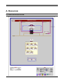
An overview of the complete hardware architecture of the system described in the next sections is included in the
appendix of this report (A.1).
Processor
The used XC5VLX110T FPGA does not have a build-in hard core processor like available in the Xilinx XC5VFX series.
Therefore a so called soft-core microprocessor needs to be implemented on the FPGA. There exists a wide range of
1
http://www.xilinx.com/univ/xupv5-lx110t-bsb.htm
5
soft microprocessor cores.2 To avoid additional licensing fees and because of the tight time schedule of the project, a
single core MicroBlaze processor was chosen. The MicroBlaze processor is a proprietary processor, developed by
Xilinx for their FPGA families and supported by the Xilinx hard- and software development kits. Its design follows
the Harvard architecture with separate data and instruction memory.
Running Linux kernel requires the presence of a MMU. This can be activated by the following settings in the project’s
MHS file for the MicroBlaze core. For using a MMU it is also required to have optimization for area disabled (default
value):
PARAMETER C_USE_MMU = 3
PARAMETER C_MMU_ZONES = 2
PARAMETER C_AREA_OPTIMIZED = 0
To improve the system performance it is recommended to enable instruction and data caches (16 KB), barrel shifter,
multiplier (64 bit) and the hardware division module. Therefore the MicroBlaze IP core settings in the MHS file
should be adjusted to meet the following values:
PARAMETER C_USE_BARREL = 1
PARAMETER C_USE_HW_MUL = 2
PARAMETER C_USE_DIV = 1
PARAMETER C_USE_ICACHE = 1
PARAMETER C_USE_DCACHE = 1
PARAMETER
PARAMETER
PARAMETER
PARAMETER
PARAMETER
PARAMETER
PARAMETER
C_CACHE_BYTE_SIZE = 16384
C_ICACHE_ALWAYS_USED = 1
C_ICACHE_LINE_LEN = 8
C_ICACHE_STREAMS = 1
C_ICACHE_VICTIMS = 8
C_DCACHE_BYTE_SIZE = 16384
C_DCACHE_ALWAYS_USED = 1
Automatic processor version recognition by the Linux Kernel (optional) can be activated by enabling the Processor
Version Register (PVR):
PARAMETER C_PVR = 2
Bus System
For connecting the MicroBlaze processor to other peripherals on the chip a bus system needs to be selected. The XPS
wizard provides an option for choosing between two interconnect types: Advanced eXtensible Interface (AXI) and
Processor Local Bus (PLB).
AXI is part of the Advanced Microcontroller Bus Architecture (AMBA), designed by ARM and introduced for FPGAs
by Xilinx starting with the Virtex-6 FPGA family generation.
Prior to the Virtex-6 FPGA family, only PLB invented by IBM as part of the CoreConnect bus system was available.
Virtex-6 FPGAs support both bus systems, but the used Xilinx XC5VLX110T FPGA is part of the Virtex-5 family,
therefore PLB needs to be selected as interconnect type. [12][p. 1, facts table]
2
see http://en.wikipedia.org/wiki/Soft_microprocessor
3.1. The Hardware System
6
Memory
The XUPV5-LX110T board contains a 9 MB ZBT synchronous SRAM, a single-rank unregistered 256 MB DDR2
SODIMM and multiple flash memory chips. The DDR2 memory fits the requirements for the desired system best.
Both regarding read and write speed, as well as the provided amount of memory.
To connect the memory to the processor a memory controller needs to be added to the system. Xilinx provides the
Multi-Port Memory Controller IP core (MPMC) – select-able in the XPS project wizard – for this purpose.
The MPMC IP core can be connected to PLB and supports Xilinx CacheLink (XCL) structures and Soft Direct Memory
Access (SDMA) for LocalLink interfaces, required for fast processing of the network interface core. [10]
The designed hardware system uses 0x50000000 as memory base address in this project. The address can be changed
arbitrarily, but needs to be adjusted accordingly in the Linux kernel configuration (see "Required Configuration
Settings", 3.2.2).
Network Interface
The Xilinx XC5VLX110T FPGA has four Tri-Mode Ethernet Media Access Controllers, designed to the IEEE 802.3-2002
specification, operating at 10, 100, and 1,000 Mb/s. [8][p. 4, table 1] To use these hard core controllers an
xps_ll_temac soft IP core can be added to the SoC, acting as a wrapper for the hard core to integrate it into the
system.
For a simple and easy-to-implement interconnection between the Physical Layer (PHY) and the various MAC
sub-layers, Media Independent Interface (MII) was invented. MII was designed originally for PHYs with data rates
of 10 Mb/s and 100 Mb/s. Gigabit Media Independent Interface (GMII) is an backwards compatible extension to
MII supporting data rates of up to 1,000 Mb/s. RMII/RGMII is an interface with reduced data path width (by half).
This is accomplished by clocking data on rising and falling edges of the clock. [5][p. 3]
For the project GMII was selected as physical interface type, because support for Gigabit Ethernet was desired, but
there was no need for a reduced data path width. Therefore the parameter C_PHY_TYPE needs to be set to 1 on the
IP core configuration.
Despite setting the C_PHY_TYPE parameter, the jumpers J22 and J23 on the Xilinx XUPV5 board need to be set to
positions 1-2 to enable GMII as physical interface type.
Depending on the (temporarily) selected FPGA during the XPS project wizard, it might be required to change the location of IDELAYCTRL elements (set by the C_IDELAYCTRL_LOC parameter) to "IDELAYCTRL_X0Y4-IDELAYCTRL_X1Y5".
Through the parameters C_TEMAC0_TXCSUM and C_TEMAC0_RXCSUM offloading checksum calculation to hardware
circuits can be enabled, to improve performance. Though there were no measurements done to prove any
performance boost during the course of this project, due to lack of time.
Other Peripherals
Besides the previously discussed IP cores, the following additional standard IP cores were used in the system, not
requiring any special explanation or configuration.
• 2x lmb_v10 – Local Memory Bus for instruction and data memory.
• bram_block – Internal Random Access Memory block on the FPGA.
• 2x lmb_bram_if_cntlr – Local Memory Bus (LMB) Block RAM (BRAM) Interface Controller for instruction
and data memory.
3.1. The Hardware System
7
• mdm – MicroBlaze Debug Module providing register access and execution control for debugging.
• xps_intc – Interrupt controller.
• 4x xps_gpio – General Purpose I/O controllers for DIP switches, LEDs and push buttons.
• xps_iic – Inter-Integrated Circuit (IIC) controller for access to external EEPROM chip.
• xps_timer – Timer block providing two independent timers.
• xps_uartlite – Universal Asynchronous Receiver Transmitter (UART) controller.
• clock_generator – Generator for system clock (configuration discussed in 3.1.4).
• proc_sys_reset – Processor System Reset Module integrating an external reset pin into the system.
The configuration settings and constraints for all IP cores as used in this project are provided in the appendix of this
report.
3.1.4 Clocks
Clock Generation
Clocks for the system can be generated using a clock_generator IP core. This IP core can generate up to 16 different
clocks from one input clock signal. On the Xilinx XUPV5 board an external oscillator providing a 100 MHz clock can
be connected to the clock generator. [11][p. 20]
Timing Considerations
After synthesis the minimum clock period is reported as 7.566 ns (i.e. a maximum clock frequency of 132.170 MHz).
Therefore it could be assumed that a 125.00 MHz system clock frequency as select-able in the XPS wizard should
work well, but the Xilinx place and route tool (par) is not able to meet all timing constraints for this frequency with
enabled MMU and instruction cache. The reason for unmet constraints are high delays on data paths in the decode
pipeline stage, demanding a clock period of about 9.12 ns.
Considering these constraints on the clock period, the system clock was set to 100 MHz. This clock is used by the
processor and the local bus.
Clock Signals for Peripherals
The memory controller (MPMC) demands atleast three different clocks: a base clock, a clock with half the frequency
of the base clock and a clock signal with the same frequency as the base clock, but shifted by 90°. If the frequency of
the base clock is not 200 MHz a fourth clock with this frequency is required. All clocks need to be controller by the
same phase-locked loop (PLL).
Therefore the clock pins of the memory controller were connected to the following signals:
PORT
PORT
PORT
PORT
MPMC_Clk0 = clk_200_0000MHzPLL0
MPMC_Clk0_DIV2 = clk_100_0000MHzPLL0
MPMC_Clk90 = clk_200_0000MHz90PLL0
MPMC_Clk_200MHz = clk_200_0000MHzPLL0
The Ethernet MAC IP core requires a clock signal with exactly 125 MHz at the GTX_CLK port for operating GMII.
This is defined in the specifications of GMII [1][sec. 35.2.2.1]. For Direct Memory Access (DMA) a clock signal
with a frequency identical to the local bus clock is required. The REFCLK needs to be connected to a 200 MHz clock,
according to the respective manual of the IP core [9][p. 11, table 3].
PORT GTX_CLK_0 = clk_125_0000MHz
3.1. The Hardware System
8
PORT REFCLK = clk_200_0000MHzPLL0
PORT LlinkTemac0_CLK = clk_100_0000MHzPLL0
The ratio between the MPMC base clock and the clock signal for LocalLink DMA access of the Ethernet MAC IP core
(200 : 100 = 2) needs to be set to the parameter C_SDMA2_PI2LL_CLK_RATIO of the MPMC core.
The clock generator is configured to generate a buffered 200 MHz clock on CLKOUT3 and a buffered 200 MHz clock
with a phase shift of 90° on CLKOUT2. All utilizing the same PLL unit (PLL0).
CLKOUT1 is configured to provide a buffered 125 MHz clock. The buffered 100 MHz system clock is set to port
CLKOUT0:
PORT
PORT
PORT
PORT
CLKOUT0
CLKOUT1
CLKOUT2
CLKOUT3
=
=
=
=
clk_100_0000MHzPLL0
clk_125_0000MHz
clk_200_0000MHz90PLL0
clk_200_0000MHzPLL0
3.1.5 Endianness
"Endianness describes how multi-byte data is represented by a computer system and is dictated by the CPU
architecture of the system." [2][p. 5]
Architectures utilizing the little endian concept store the least significant byte (LSB) at the lowest address, in big
endian architectures the most significant byte (MSB) is stored at the highest address. [2][p. 6]
Linux can be build for little, as well as for big endian systems. Only confinement is that the used toolchain (compiler,
etc. - see 3.2.2) needs to support the endianness of the architecture.
The MicroBlaze processor has the parameter C_ENDIANNESS to specify the endianness of the processor. But although
the MicroBlaze Processor Reference Guide states that "the C_ENDIANNESS parameter is automatically set to little endian
when using AXI4, and to big endian when using PLB, but can be overridden by the user" [13][p. 52], this parameter
must not be changed for Virtex-5 FPGAs. This is reasoned in the disability of the peripheral cores connected via PLB,
to handle data other than in big endian byte order. The AXI bus circumvents this problem by swapping bytes.3
Therefore big endian must be selected for the system architecture of this project.
3.1.6 Generating the Hardware System
As discussed in the sub section about FPGAs, a bitstream needs to be generated from the MHS and constraint files.
Therefore the hardware design must be implemented by triggering the "Implement Design" process listed in the
Xilinx ISE Project Navigator. In a second step the bitstream file (<project-name>.bit) can be generated from the
implemented design, by triggering the "Generate Programming File" process.
Additionally the hardware design can be exported to the Xilinx SDK. This is required for generating small C projects
for testing the hardware and single IP cores and the generation of further, intermediate configuration files (see
"Device Tree", 3.2.2).
3.2 The Software
3
http://forums.xilinx.com/t5/EDK-and-Platform-Studio/Memory-Test-fails-for-8-and-16-bit/m-p/253922/highlight/
true#M23973 (in-official statement by a Xilinx employee)
3.2. The Software
9
3.2.1 Linux Kernel
Running Linux on a MicroBlaze processor is unfortunately rarely documented and not wide spread. Mainly two
projects exist on this topic: PetaLinux and BlueCat Linux. Unfortunately both were turned into commercial solutions
and although the patched Linux source code is publicly available, it is hardly usable without the proprietary toolkit,
documentation and support, sold by the companies driving these projects.
When talking about Linux, it needs to be distinguished between the Linux kernel as the actual OS and Linux
distributions (like Ubuntu, Debian, openSUSE, Fedora and many more), containing additional libraries, applications
and configuration. The Linux kernel in itself is the heart of a Linux installation. There exists one major development
line (called "mainline"), being maintained by a group around the founder of Linux, Linus Torvalds. But there exist
also also copies of the source code (called "fork") with incorporated custom changes.
Originally support for MicroBlaze soft-core processors in the Linux kernel was developed by Xilinx and PetaLogix in
an own fork of Linux kernel, but with version 2.6.30, released on the 9th of June 2009, their additions were merged
into the mainline Linux kernel and the MicroBlaze architecture is officially supported by Linux since this date.4 The
still maintained and actively used source code repositories of Xilinx5 and PetaLogix6 contain some further additions
to device drivers and unreleased changes.
For this project the Linux kernel source code from the Xilinx repository was taken. All development, additions and
evaluation was done on top of commit ed63a4d76efadcb68f5776e4244766ffea226cc4 (June, 18th 2012)7 as part
of version 3.3.0-14.2-build1.
To enable correct recognition of the latest MicroBlaze processor versions with enabled PVR a patch included in the
appendix of this report (A.3.2) needs to be applied to the Linux kernel sources. The patch was extracted from the
PetaLogix Linux kernel fork.
3.2.2 Development Environment and Cross Compilation
To build the Linux kernel a set of tools (called toolchain) compiling source code files and linking binary output in an
executable file is required. This toolchain needs to meet two criteria: the architecture/OS it was build to run on top
and the target architecture for which images are compiled and linked. Building an image with a different target
architecture, than the architecture of the executing system, is called cross compilation. Because it is not practically
possible to build the Linux kernel on a MicroBlaze processor, without an existing and running OS on the MicroBlaze
system, a toolchain for cross compiling Linux kernel source from an existing, easily-usable system for a MicroBlaze
system, is needed. Xilinx provides toolchains, based on the widely used GNU Compiler Collection (GCC) and binutils,
for cross compiling from Linux x86 and x86-64 architectures to MicrobBlaze systems as target architecture. For
compiling the latest Linux kernel sources, version two of the toolchain containing GCC in version 4.1.2 is required.
This version of the toolchain itself requires a 64-bit Linux OS and can be downloaded from the Xilinx source code
repositories.8
During this project a virtual Linux machine with Ubuntu 12.04 64-bit was used for all software development.
To enable cross compilation of the Linux kernel, two environment variables need to be set. The CROSS_COMPILE
variable specifies a prefix for all build tools. This is required, because on cross compilation there is usually more
than one compiler available on the executing system. Furthermore the path to the utilized build tools needs to be
added to the PATH variable.
4
5
6
7
8
http://www.petalogix.com/news/microblaze-architecture-merged-into-kernel.org
http://git.xilinx.com/?p=linux-xlnx.git
http://developer.petalogix.com/git/gitweb.cgi?p=linux-2.6-microblaze.git
http://git.xilinx.com/?p=linux-2.6-xlnx.git;a=commit;h=ed63a4d76efadcb68f5776e4244766ffea226cc4
http://git.xilinx.com/?p=xldk/microblaze_v2.0.git
3.2. The Software
10
The ARCH variable enables the inclusion of code specific to the target architecture. This code files reside in
/arch/<ARCH>/ inside the Linux kernel source folder.
The environment variables can be set as parameter on build execution or for the complete shell session with the
following commands:
export PATH=/<path>/<to>/microblaze-unknown-linux-gnu/bin:$PATH
export CROSS_COMPILE=microblaze-unknown-linux-gnuA build process is triggered by calling the make executable inside of the Linux kernel source folder. Here an example
for triggering a new build of the Linux kernel for the MicroBlaze architecture, utilizing two processor cores:
make -j 2 ARCH=microblaze simpleImage.xupv5
simpleImage specifies the image format, xupv5 is an additional configuration option explained in the Device Tree
section (3.2.2).
The Linux Configuration System
Linux kernel consists of many optional sub-parts for target architectures, device drivers, special features, etc. Which
of these parts are compiled and linked into the Linux kernel binary image needs to be configured in the .config file
in the Linux kernel root directory. This file is "the configuration blueprint for building a Linux kernel image" [4][sec.
4.3.1] containing all (required) settings.
Although possible, it is not recommended to edit the .config file manually, because of many non-trivial dependencies
among different configuration settings. Instead one of the available editors (menuconfig, xconfig and gconfig) should
be used. Because of its search capabilities inside the configuration settings, xconfig was used as configuration editor
during this project.9
Before starting a new project all existing configuration and temporary output files should be cleaned up using the
commands "make ARCH=microblaze clean" and "make ARCH=microblaze mrproper".
In the Linux kernel fork maintained by Xilinx a base configuration for the ML507 board is included. It is recommended
to use this configuration as base line instead of starting from scratch. The configuration can be loaded using the
following command:
make ARCH=microblaze xilinx_mmu_defconfig
From there on the configuration can be viewed and edited using a configuration editor with the following command:
make ARCH=microblaze xconfig
Required Configuration Settings
As discussed in 3.1.3, the MicroBlaze processor can be configured with different feature sets (multiplier, barrel shifter,
etc.). Therefore the GCC compiler needs to be parameterized for matching the provided features of the target system
[14][sec. "Kernel Configuration Details"]. These need to be set in the XILINX_MICROBLAZE0_* settings inside of the
.config file.
It is important to check that the KERNEL_BASE_ADDR setting is in line with the configured base address of the main
memory (C_MPMC_BASEADDR) in the MHS file.
9
xconfig requires the QT library which can be installed through the package qt4-dev-tools on Debian and Ubuntu distributions.
3.2. The Software
11
For inclusion of the driver for the xps_ll_temac IP core, the configuration option XILINX_LL_TEMAC needs
to be enabled.
Support for UART device drivers can be enabled by the settings SERIAL_UARTLITE,
SERIAL_UARTLITE_CONSOLE, SERIAL_CORE and SERIAL_CORE_CONSOLE, but this is already included in the default
ML507 configuration settings provided by Xilinx.
When there is no boot loader triggering Linux kernel start, command-line options for the boot process need to
be compiled into the Linux kernel image. Therefore the configuration setting CMDLINE exists. The command-line
options for this project were set as follows:
CONFIG_CMDLINE = "console=ttyUL0 root=/dev/ram rw"
ttyUL0 sets the first serial device (index 0) of type uartlite (UL) as default console and loads the RAM image with
read and write access (rw) as root file system (see "The File System" 3.2.3).
Additionally some features like IPv6 support and various security algorithms were enabled in the Linux kernel
configuration. The complete .config file with all settings is referenced in the report appendix.
Device Tree
To avoid compiling all information about the target hardware system into assembler code, an abstraction called
Device Tree was invented. Device Tree is the successor of IBM’s Open Firmware (OF) and the flattened device tree,
containing information about the hardware system like available feature sets and bus addresses. [3] It is accessed by
the Linux kernel during the boot process for configuring itself and on lookup of hardware information. The Device
Tree Source (dts) file is compiled by the Device Tree Compiler (dtc) during the Linux kernel build process to an Device
Tree Blob (dtb) and linked into the final Linux kernel image.
The dts file must reside inside of the arch/microblaze/boot/dts directory (e.g. "arch/microblaze/boot/dts/xupv.dts")
and can be specified on starting the Linux kernel build process (e.g. "make ARCH=microblaze simpleImage.xupv5").
A dts file can be generated using the Device Tree Generator, a Tool command language (TCL) script reading a system
specification generated by XPS (see "SDK Export"). The latest version (1.3) of the Device Tree Generator, maintained
by Michal Simek, is referenced in the appendix of this report (A.3.5).
Apart from the generated device information, the dts file also contains options which must be set manually. These
include an aliases node for mapping device instances to standardized interface names (ethernet0 and serial0)
and command-line options, overriding10 the ones specified in the Linux kernel configuration file. Additionally the
stdout device bus address can be set:
aliases {
ethernet0 = &Hard_Ethernet_MAC;
serial0 = &RS232_Uart_1;
} ;
chosen {
bootargs = "console=ttyUL0 ip=192.168.3.10 root=/dev/ram";
linux,stdout-path = "/plb@0/serial@84020000";
} ;
Besides the options already explained in the "Required Configuration Settings" section (3.2.2), this configuration
assigns the logical IPv4 address 192.168.3.10 to the network interface of the board.
The Device Tree Generator can be setup as own BSP inside of the Xilinx SDK. A documentation with all required steps
for setting it up can be found on the respective site hosted by Xilinx.11
10
11
By setting the kernel configuration option CMDLINE_FORCE to "y", the command-line options specified in the .config file take precedence.
http://wiki.xilinx.com/device-tree-generator
3.2. The Software
12
3.2.3 The File System
Although possible, it makes little sense to use the Linux kernel without a file system. Therefore one of the last steps
in the boot process is the initialization of a root file system (rootfs). [4][sec. 6.1] On modern desktop and server
systems this rootfs is usually just a bare minimum file system, containing all necessary files to boot the Linux kernel,
mounting a file system located on a hard drive or flash memory right after booting up. But the used system in this
project has no hard drive attached, neither is one required for the purpose of the project, at the moment. Therefore
we will stick with the initial rootfs as the main file system.
A simple way to provide an initial rootfs is the Initial RAM Disk (initrd). This is a file system packed in a cpio
archive and linked into the Linux kernel image. It is unpacked completely into the main memory during kernel
boot process. Xilinx provides two packed file system archives for a MicroBlaze system within their Linux kernel
repository: initramfs_minimal.cpio.gz and initramfs_complete.cpio.gz. Both contain all files and structures
sufficient for this project. The archives can be linked into the Linux kernel image by setting the configuration option
INITRAMFS_SOURCE to one of the file names, respectively.
cpio archives can be unpacked using the following command. This command should be executed as privileged root
user to allow the creation of node points, used in the file system.
gzip -dc /<path>/<to>/initramfs_complete.cpio.gz | sudo cpio -i
After all changes were made to the files representing the file system, it can be packed into a cpio archive using the
bash script supplied in the appendix of this report ("pack-fs.sh", A.3.4). The paths to the Linux kernel sources and
file system root need to be adjusted to meet the current environment.
3.2.4 Deployment and Debugging
The generated bitstream of the hardware system representing the SoC, needs to be programmed into the FPGA
on every power-on. This is required, because the configuration of the FPGA being set by the bitstream is volatile.
Programming the bitstream is straight forward and can be accomplished using the Xilinx iMPACT tool, which is part
of the Xilinx ISE Design Suite.
When the Linux kernel build is finished, the resulting Executable and Linkable Format (ELF) file can be found at
arch/microblaze/boot/simpleImage.<dts-name>. This file can be loaded into the FPGA using Xilinx Microprocessor Debug Engine (XMD), which is also part of the Xilinx ISE Design Suite. The steps for loading an ELF file onto a
FPGA with MicroBlaze processor using XMD are as follows:
1. Connecting to the MicroBlaze processor:
xmd> connect mb mdm
2. Stopping the MicroBlaze processor:
xmd> stop
3. Downloading the ELF file:
xmd> dow simpleImage.<dts-name>
4. Starting the MicroBlaze processor:
xmd> con
After committing these steps the Linux kernel boot log should be written to the connected serial interface. However,
when there are problems in the early boot process, the console output might not have been initialized yet. If this is
the case, the content written to the console output can be read and decoded from memory manually. It is stored in
the global variable "__log_buf".
3.2. The Software
13
Reading the __log_buf variable from memory and decoding the binary representation of the content can be
accomplished using the TCL script included in the report appendix (syslog.tcl, A.3.3). It is a ported version for
MicroBlaze processors of the script supplied with the Xilinx Application Note XAPP113712 .
One thing that needs to be adjusted according to the Linux kernel image is the start address of the __log_buf
variable (at line 6, "set bufaddr <addr>"). This address can be determined by executing the command "xmd>
mrd_var __log_buf" inside of XMD. The command returns the word stored at the first address of the variable and
the address of the variable itself: "__log_buf(<address>) <data>". After saving the TCL script to a file it can be
loaded into a XMD session using the command "xmd> source syslog.tcl". The script writes all the content of the
__log_buf variable to the file "syslog_1.txt" and can be executed using the command "xmd> syslog".
3.2.5 Testing the System
Full functionality of the system, including the network interface, can be tested by connecting a computer to the
Ethernet port of the board and starting a small web server on the MicroBlaze processor.
This can be done executing the following commands on the console connected to the system:
mkdir /var/www
echo "Hello FPGA!" > /var/www/index.html
httpd -p 80 -h /var/www
The network interface of the connected computer needs to be configured to be part of the subnet 192.168.3.0/24,
except the address 192.168.3.10 which is assigned to the system on the board.
The test site returning the content "Hello FPGA!" can be accessed from the connected computer by visiting the site
http://192.168.3.10/ in a web browser.
12
http://www.xilinx.com/support/documentation/application_notes/xapp1137.pdf
3.2. The Software
14
4 Conclusion
4.1 Project Review and Evaluation
I chose this project, because it promised to cover many topics of personal interest, including network systems,
performance oriented research and optimization, web technology and System on chip design. In retrospective these
expectations were fulfilled, but came with a steep learning curve.
After some weeks of administrative problems concerning setup of the environment and required tools, the project
could get started. The following two to three weeks were filled with learning the utilized tools and understanding
the overall process of designing an IP core based SoC on a FPGA. When being familiar with the general concepts and
topics covered by this project, I started to focus on the actual project goal, assembled a time schedule and defined
an, from my point of view at that time, doable intermediate goal for the project seminar. But as it turned out during
the course of the project, it was hardly possible to stick to the schedule and the planned outcome of the project
seminar. This was mainly reasoned in lots of problems occurring at points, which initially seemed to be straight
forward implementation tasks, but in fact contained many non-trivial pitfalls.
One of the major difficulties solved during this project seminar was the fact that there exists some documentation
and reference projects (partly) covering the project objective, on the one hand, but these could not be ported easily
to the tools and hardware family used in this project. This was especially a problem, because Xilinx makes little effort
to keep new versions of their tools and included IP cores compatible with older hardware families. Discovering and
keeping this circumstance in mind, was one of the key points in successfully implementing the described outcome of
the project seminar.
All in all working through this project seminar was a hard but valuable experience, especially learning about all the
interfaces and dependencies between the different levels in the stack of a computer system.
4.2 Outlook
The project seminar covered only the first part of the project goal. So there is naturally some work to be done to
finish the project. This covers especially everything around incorporating custom user space applications (like nginx)
and an accurate measurement and evaluation of performance parameters of the designed system.
Besides these outstanding topics, improvements to already implemented parts of the system could be made, too. To
name a few, the baud rate of the serial IP core could be increased to enable a more responsive console interface for
accessing the system. An additional, non-volatile file system could be added to the system to circumvent the need
for programming a complete image onto the FPGA on every persisted change to the file system. This could be done
by including a Network File System (NFS) or a file system stored on a flash drive.
When the complete system is implemented, including the event-based server, as stated in the project title, the focus
of the project work needs to be shifted more towards measuring the performance parameters of the system. As part
of this work an "TCP Offload Engine", designed in a parallel project could be incorporated into the system. Purpose
of this offload engine is to fork processing load resulting from incoming and outgoing network traffic from the CPU
to a designated hardware core. It is expected that this will speed up the overall performance of the system, allowing
either the usage of less hardware resources or a higher network throughput.
The next steps in a subsequent project seminar or bachelor thesis would be to get cross compilation of user space
applications working, incorporate nginx into the system and conduct the mentioned performance measurements.
15
Bibliography
[1] 802.3-2000 - part 3: Carrier sense multiple access with collision detect on (csma/cd) access method and
physical layer specifications. IEEE Std 802.3, 2000 Edition, pages i –1515, 2000.
[2] Intel Corporation. Endianness White Paper. http://www.intel.com/design/intarch/papers/endian.pdf,
11 2004.
[3] David Gibson and Benjamin Herrenschmidt. Device trees everywhere. http://ozlabs.org/~dgibson/papers/
dtc-paper.pdf, 2 2006.
[4] Christopher Hallinan. Embedded Linux Primer: A Practical Real-World Approach. Prentice Hall PTR, Upper
Saddle River, NJ, USA, 2006.
[5] HP, Broadcom, and Marvel. Reduced Gigabit Media Independent Interface(RGMII). http://www.hp.com/rnd/
pdfs/RGMIIv1_3.pdf, 1.3 edition, 12 2000.
[6] National Instruments. FPGA Fundamentals. http://www.ni.com/white-paper/6983/en. called 08/28/2012.
[7] Xilinx. XUPV5-LX110T User Manual. http://www.xilinx.com/univ/xupv5-lx110T-manual.htm. called
09/06/2012.
[8] Xilinx. Virtex-5 Family Overview (DS100). http://www.xilinx.com/support/documentation/data_sheets/
ds100.pdf, v5.0 edition, 2 2009.
[9] Xilinx. LogiCORE IP XPS LL TEMAC. http://www.xilinx.com/support/documentation/ip_documentation/
xps_ll_temac.pdf, v2.03a edition, 12 2010.
[10] Xilinx.
LogiCORE IP Multi-Port Memory Controller (DS643).
http://www.xilinx.com/support/
documentation/ip_documentation/mpmc.pdf, v6.05a edition, 10 2011.
[11] Xilinx. ML505/ML506/ML507 Evaluation Platform - User Guid (UG347). http://www.xilinx.com/support/
documentation/boards_and_kits/ug347.pdf, v3.1.2 edition, 5 2011.
[12] Xilinx.
LogiCORE IP AXI Interconnect.
http://www.xilinx.com/support/documentation/ip_
documentation/axi_interconnect/v1_06_a/ds768_axi_interconnect.pdf, v1.06a edition, 4 2012.
[13] Xilinx. MicroBlaze Processor Reference Guide (UG081). http://www.xilinx.com/support/documentation/
sw_manuals/xilinx14_1/mb_ref_guide.pdf, 14.1 edition, 4 2012.
[14] Xilinx et al. MicroBlaze Linux (General). http://wiki.xilinx.com/microblaze-linux.
16
A Resources
A.1 Hardware Architecture Overview
17
A.2 Hardware Project Configurations
The configuration files contain more than 800 lines, being too much to include them directly in the project
report. Therefore the Microprocessor Hardware Specification (mhs) and User Constraint File (ucf) files can be
downloaded as part of the projects for XPS and the Xilinx ISE Project Navigator from the following address:
http://www.peschuster.de/ies-project/IesHttpProject-Hardware.zip.
A.3 Linux Kernel Assets
A.3.1 Configuration
The Linux kernel configuration file contains more than 1,200 lines and is therefore not included directly within this
appendix, but can be downloaded together with all other scripts concerning the software part of this project from
the following address: http://www.peschuster.de/ies-project/IesHttpProject-Software.zip.
Here are the configuration settings specific for the MicroBlaze processor used in this project:
CONFIG_KERNEL_BASE_ADDR=0x50000000
CONFIG_XILINX_MICROBLAZE0_FAMILY="virtex5"
CONFIG_XILINX_MICROBLAZE0_USE_MSR_INSTR=1
CONFIG_XILINX_MICROBLAZE0_USE_PCMP_INSTR=1
CONFIG_XILINX_MICROBLAZE0_USE_BARREL=1
CONFIG_XILINX_MICROBLAZE0_USE_DIV=1
CONFIG_XILINX_MICROBLAZE0_USE_HW_MUL=2
CONFIG_XILINX_MICROBLAZE0_USE_FPU=0
CONFIG_XILINX_MICROBLAZE0_HW_VER="8.30.a"
A.3.2 Patches
Path for correct recognition of the latest MicroBlaze processor versions with enabled PVR:
commit 9be0160c855d1740f392d74a90197421c1380946
Author: Peter Schuster <[email protected]>
Date:
Sat Sep 8 19:48:56 2012 +0200
Added new MicroBlaze versions.
diff --git a/arch/microblaze/kernel/cpu/cpuinfo.c b/arch/microblaze/kernel/cpu/cpuinfo.c
index 54194b2..783c7087 100644
--- a/arch/microblaze/kernel/cpu/cpuinfo.c
+++ b/arch/microblaze/kernel/cpu/cpuinfo.c
@@ -35,6 +35,8 @@ const struct cpu_ver_key cpu_ver_lookup[] = {
{"8.00.b", 0x13},
{"8.10.a", 0x14},
{"8.20.a", 0x15},
+
{"8.20.b", 0x16},
+
{"8.30.a", 0x17},
{NULL, 0},
};
The patch file "new-microblaze-versions.patch" is also included in the zip archive available at http://www.
peschuster.de/ies-project/IesHttpProject-Software.zip.
A.2. Hardware Project Configurations
18
A.3.3 syslog.tcl
proc mb_mrd_w { address } {
return 0x[ string range [mrd $address 1 w] 12
}
19]
proc syslog { } {
set bufaddr 0xc04d3c30
set bufsize 0x00020000
set startaddr $bufaddr
set endaddr [expr $bufaddr + $bufsize]
set fp [open "syslog_1.txt" w]
puts $fp "Displaying Linux syslog buffer of $bufsize length at $bufaddr"
while {$startaddr < $endaddr} {
# Read 4 bytes of text
set mval [ mb_mrd_w $startaddr ]
# Display the word of text, a byte at a time
set shift 24
while {$shift >= 0} {
set char [expr [expr $mval >> $shift] & 0xff]
# NULL ? End of string.
if {$char == 0} {
return
}
set char [format "%c" $char]
puts -nonewline $fp "$char"
incr shift -8
}
incr startaddr 4
}
puts $fp ""
close $fp
}
The file "syslog.tcl" is also included in the zip archive available at http://www.peschuster.de/ies-project/
IesHttpProject-Software.zip.
A.3.4 pack-fs.sh
#!/bin/bash
f=‘dirname "$0"‘
cd "$f/complete"
find . -print | cpio -H newc -o | gzip > "../complete_fs.cpio.gz"
A.3. Linux Kernel Assets
19
The file "pack-fs.sh" is also included in the zip archive available at http://www.peschuster.de/ies-project/
IesHttpProject-Software.zip.
A.3.5 Device Tree Generator and Source
The latest version of the Device Tree Generator BSP can be downloaded from the site of Michal Simek (http:
//www.monstr.eu/wiki/lib/exe/fetch.php?media=fdt:fdt:logs:device-tree_latest.tar.gz.
It is also available in version 1.3 from the url http://www.peschuster.de/ies-project/device-tree-1-3.zip,
as used in this project.
The dts file (xupv5.dts) for the hardware system used in this project is part of the zip archive available at
http://www.peschuster.de/ies-project/IesHttpProject-Software.zip.
A.4 Image files
The bitstream (system.bit) and Linux kernel image (simpleImage.xupv5) files for the Xilinx XUPV5-LX110T
board and described hardware system are available for download at http://www.peschuster.de/ies-project/
IesHttpProject-Images.zip.
A.4. Image files
20

![2008 [DAMN SMALL NAS]](http://vs1.manualzilla.com/store/data/005757702_2-ad0d2f1082977ee9ed587e807bbc0127-150x150.png)