1
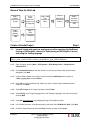
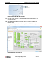
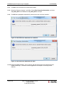
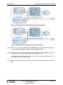
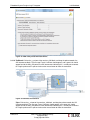
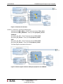
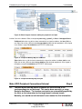
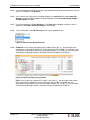
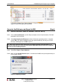
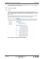
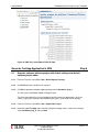
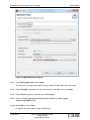
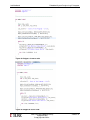
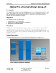
Lab Workbook
Embedded System Design using IP Integrator
Embedded System Design using IP Integrator
Introduction
This lab guides you through the process of using Vivado and IP Integrator to create a simple ARM
Cortex-A9 based processor design targeting either the ZedBoard or the Zybo development board. You
will use IP Integrator to create the hardware block diagram and SDK (Software Development Kit) to
create an example application to verify the hardware functionality.
Objectives
After completing this lab, you will be able to:
• Create a Vivado project for a Zynq system
• Use the IP Integrator to create a hardware system
• Use IP Catalog to use AXI GPIO peripheral to extend the design
• Use SDK to create a standard memory test project
• Run the test application on the board
Procedure
This lab is separated into steps that consist of general overview statements that provide information on
the detailed instructions that follow. Follow these detailed instructions to progress through the lab.
Design Description
The purpose of the lab exercise is to walk you through a complete hardware and software processor
system design. The following diagram represents the completed design (Figure 1).
In this lab, you will use IP Integrator to create a processing system based design consisting of the
following:
• ARM Cortex A9 core (PS)
• UART for serial communication
• DDR3 controller for external DDR3_SDRAM memory
• AXI Interconnect block
• Two instances of GPIO peripheral to connect push-buttons and slide switches
Figure 1. Processor Design of this Lab
www.xilinx.com/support/university
[email protected]
© copyright 2014 Xilinx
ZYNQ 3-1
Embedded System Design using IP Integrator
Lab Workbook
General Flow for this Lab
Step 1:
Create a
project using
Vivado
Step 6:
Create a
Memory
TestApp in
SDK
Step 2:
Create
Processor
System using
IP Integrator
Step 3: Add
Two
Instances of
GPIO
Step 4:
Make GPIO
Connections
External
Step 5:
Generate
Bitstream
and Export to
SDK
Step 7:
Verify
Functionality
in Hardware
Create a Vivado Project
1-1.
Step 1
Launch Vivado and create an empty project either targeting the ZedBoard
(having xc7z020clg484-1 device) or Zybo (having xc7z010clg400-1 device)
and using the Verilog language.
References to <2014_2_zynq_labs> means c:\xup\sys_design\2014_2_zynq_labs and
<2014_2_zynq_sources> means c:\xup\sys_design\2014_2_zynq_sources directories.
1-1-1. Open Vivado by selecting Start > All Programs > Xilinx Design Tools > Vivado 2014.2 >
Vivado 2014.2
1-1-2. Click Create New Project to start the wizard. You will see the Create a New Vivado Project
dialog box. Click Next.
1-1-3. Click the Browse button of the Project Location field of the New Project form, browse to
<2014_2_zynq_labs>, and click Select.
1-1-4. Enter lab3 in the Project Name field. Make sure that the Create Project Subdirectory box is
checked. Click Next.
1-1-5. Select RTL Project in the Project Type form, and click Next.
1-1-6. Select Verilog as the Target language and as the Simulator language in the Add Sources form,
and click Next.
1-1-7. Click Next two more times to skip Adding Existing IP and Add Constraints
1-1-8. In the Default Part form, select Boards specify, and either select ZedBoard or Zybo. Click Next.
1-1-9. Check the Project Summary and click Finish to create an empty Vivado project.
ZYNQ 3-2
www.xilinx.com/support/university
[email protected]
© copyright 2014 Xilinx
Lab Workbook
Embedded System Design using IP Integrator
Create the System Using the IP Integrator
2-1.
Step 2
Use the IP Integrator to create a new Block Design, and generate the ARM
Cortex-A9 processor based hardware system.
2-1-1. In the Flow Navigator pane, click Create Block Design under IP Integrator
2-1-2. Enter system for the design name and click OK.
Figure 2. Create New Block Diagram
2-1-3. IP from the catalog can be added in different ways. Click on Add IP in the message at the top of
the Diagram panel, or click the Add IP icon
in the block diagram side bar, press Ctrl + I, or
right-click anywhere in the Diagram workspace and select Add IP
Figure 3. Add IP to Block Diagram
www.xilinx.com/support/university
[email protected]
© copyright 2014 Xilinx
ZYNQ 3-3
Embedded System Design using IP Integrator
Lab Workbook
2-1-4. Once the IP Catalog is open, type “zy” into the Search bar, find and double click on ZYNQ7
Processing System entry, or click on the entry and hit the Enter key to add it to the design.
Figure 4. Add Zynq block to the design
2-1-5. Notice the message at the top of the Diagram window that Designer Assistance available. Click
on Run Block Automation and select /processing_system7_0
Figure 5. Designer Assistance message
2-1-6. Click OK when prompted to run automation.
Figure 6. Run Block Automation
Once Block Automation has been complete, notice that ports have been automatically added for
the DDR and Fixed IO, and some additional ports are now visible. A default configuration for the
Zynq depending on the target board has been applied which will now be modified.
ZYNQ 3-4
www.xilinx.com/support/university
[email protected]
© copyright 2014 Xilinx
Lab Workbook
Embedded System Design using IP Integrator
Figure 7. Zynq Block with DDR and Fixed IO ports
2-1-7. In the block diagram, double click on the Zynq block to open the Customization window for the
Zynq processing system.
2-1-8. A block diagram of the Zynq should now be open, showing various configurable blocks of the
Processing System.
At this stage, the designer can click on various configurable blocks (highlighted in green) and
change the system configuration.
Figure 8: Zynq System Configuration View
www.xilinx.com/support/university
[email protected]
© copyright 2014 Xilinx
ZYNQ 3-5
Embedded System Design using IP Integrator
2-2.
Lab Workbook
Configure I/O Peripherals block to use UART 1 only
Only the UART is required for this lab, so all other peripherals will be deselected.
2-2-1. Click on one of the peripherals (in green) in the IOP Peripherals block, or select the MIO
Configuration tab in the Page Navigator on left to open the configuration form
2-2-2. Expand I/O peripherals if necessary, and deselect all the I/O peripherals except UART 1.
i.e. Remove:
ENET 0
USB 0
SD 0
Expand GPIO to deselect GPIO MIO
Expand Memory Interfaces to deselect Quad SPI Flash
Expand Application Processor Unit to deselect Timer 0.
Figure 9. Selecting only UART 1
2-2-3. Click on the Clock Configuration, expand PL Fabric Clocks, and observe that FCLK_CLK0 is
enabled with 100 MHz frequency.
ZYNQ 3-6
www.xilinx.com/support/university
[email protected]
© copyright 2014 Xilinx
Lab Workbook
Embedded System Design using IP Integrator
2-2-4. Click OK.
We left the rest of the configuration as is since we want to add two GPIO peripherals in the PL
section which will be connected through the GP0 master interface, using FCLK_CLK0 as the
clock source and FCLK_RESET0_N as the reset control signal.
Figure 10. Updated Zynq Block
Add Two Instances of GPIO
3-1.
Step 3
Add two instances of the GPIO Peripheral from the IP catalog to the
processor system.
3-1-1. Click the Add IP icon
and search for “gp”.
Figure 11. Add GPIO IP
3-1-2. Double-click the AXI GPIO to add the core to the design. The core will be added to the design
and the block diagram will be updated.
Figure 12. Zynq system with AXI GPIO added
3-1-3. Click on the AXI GPIO block to select it, and in the properties tab,
ZedBoard: Change the name to sw_8bit
www.xilinx.com/support/university
[email protected]
© copyright 2014 Xilinx
ZYNQ 3-7
Embedded System Design using IP Integrator
Lab Workbook
Figure 13: Change AXI GPIO default name
Zybo: Change the name to sw_4bit
Figure 13. Change AXI GPIO default name
3-1-4. Double click on the AXI GPIO block to open the customization window.
If a board specify was selected during the project creation, and board files were available for the
Zybo, Vivado has knowledge of available resources on the board.
3-1-5. Click on Generate Board Based IO Constraints, and under Board Interface, for GPIO.
ZedBoard: Click on Custom to view the dropdown menu options, and select sws 8bits
Figure 14: Configuring GPIO instance for switches on ZedBoard
ZYNQ 3-8
www.xilinx.com/support/university
[email protected]
© copyright 2014 Xilinx
Lab Workbook
Embedded System Design using IP Integrator
Zybo: Click on Custom to view the dropdown menu options, and select sws 4bits
Figure 14. Configuring GPIO instance for switches on Zybo
3-1-6. Click the IP Configuration tab. Notice the set GPIO Width.
Notice that the peripheral can be configured for two channels, but, since we want to use only one
channel without interrupt, leave the GPIO Supports Interrupts and Enable Channel 2 unchecked.
ZedBoard: The GPIO width is set to 8.
Figure 15. Configuring GPIO instance for ZedBoard
Zybo: The GPIO width is set to 4.
Figure 15. Configuring GPIO instance for Zybo
www.xilinx.com/support/university
[email protected]
© copyright 2014 Xilinx
ZYNQ 3-9
Embedded System Design using IP Integrator
Lab Workbook
3-1-7. Click OK to save and close the customization window
3-1-8. Notice that Design assistance is available. Click on Run Connection Automation, and select
/sw_8bit/S_AXI for the ZedBoard or /sw_4bit/S_AXI for the Zybo.
3-1-9. Click OK when prompted to automatically connect the master and slave interfaces
Figure 16. Run Connection Automation for ZedBoard
Figure 16. Run Connection Automation for Zybo
3-1-10. Notice two additional blocks, Proc Sys Reset, and AXI Interconnect have automatically been
added to the design. (The blocks can be dragged to be rearranged, or the design can be
redrawn.)
ZYNQ 3-10
www.xilinx.com/support/university
[email protected]
© copyright 2014 Xilinx
Lab Workbook
Embedded System Design using IP Integrator
Figure 17: Design with sw_8bit automatically connected for ZedBoard
Figure 17. Design with sw_4bit automatically connected for Zybo
3-1-11. Add another instance of the GPIO peripheral (Add IP), and using the board flow, configure it to
connect to either the btns 5bit on ZedBoard or the btns 4bits on Zybo.
3-1-12. Change the name of the block either to btns_5bit for ZedBoard or to btns_4bit for Zybo (Click
on the block to select it, and change the name in the properties view)
At this point connection automation could be run, or the block could be connected manually. This
time the block will be connected manually.
3-1-13. Double click on the AXI Interconnect and change the Number of Master Interfaces to 2 and click
OK
www.xilinx.com/support/university
[email protected]
© copyright 2014 Xilinx
ZYNQ 3-11
Embedded System Design using IP Integrator
Lab Workbook
Figure 18. Add slave port to AXI Interconnect
3-1-14. ZedBoard: Click on the s_axi port of the new btns_5bit block, and drag the pointer towards the
AXI Interconnect block. The message Found 1 interface should appear, and a green tick should
appear beside the M01_AXI port on the AXI Interconnect indicating this is a valid port to connect
to. Drag the pointer to this port and release the mouse button to make the connection.
Figure 19: Connect the interfaces
Zybo: Click on the s_axi port of the new btns_4bit block, and drag the pointer towards the AXI
Interconnect block. The message Found 1 interface should appear, and a green tick should
appear beside the M01_AXI port on the AXI Interconnect indicating this is a valid port to connect
to. Drag the pointer to this port and release the mouse button to make the connection.
ZYNQ 3-12
www.xilinx.com/support/university
[email protected]
© copyright 2014 Xilinx
Lab Workbook
Embedded System Design using IP Integrator
Figure 19. Connect the interfaces
3-1-15. In a similar way, connect the following ports:
AXI Interconnect M01_ACLK -> Zynq7 Processing System FCLK_CLK0
AXI Interconnect M01_ARESETN -> Proc Sys Reset peripheral_aresetn
ZedBoard:
btns_5bit s_axi_aclk -> Zynq7 Processing System FCLK_CLK0
btns_5bit s_axi_aresetn -> Proc Sys Reset peripheral_aresetn
Zybo:
btns_4bit s_axi_aclk -> Zynq7 Processing System FCLK_CLK0
btns_4bit s_axi_aresetn -> Proc Sys Reset peripheral_aresetn
The block diagram should look similar to this:
Figure 20. Block diagram view after adding the peripherals for ZedBoard
www.xilinx.com/support/university
[email protected]
© copyright 2014 Xilinx
ZYNQ 3-13
Embedded System Design using IP Integrator
Lab Workbook
Figure 20. Block diagram view after adding the peripherals for Zybo
3-1-16. Click on the Address Editor, and expand processing_system7_0 > Data > Unmapped Slaves.
ZedBoard: Notice that sw_8bit has been automatically assigned an address, but btns_5bit has
not. Right click on btns_5bit and select Assign Address. Note that both peripherals are assigned
in the address range of 0x40000000 to 0x7FFFFFFF (GP0 range).
Figure 21. Peripheral Memory Map for ZedBoard
Zybo: Notice that sw_4bit has been automatically assigned an address, but btns_4bit has not.
Right click on btns_4bit and select Assign Address. Note that both peripherals are assigned in
the address range of 0x40000000 to 0x7FFFFFFF (GP0 range).
Figure 21. Peripherals Memory Map for Zybo
Make GPIO Peripheral Connections External
4-1.
Step 4
The push button and dip switch instances will be connected to the
corresponding pins on the board. This can be done manually, or using
Designer Assistance. The location constraints are automatically applied by
the tools as the information for the target board is already known.
Normally, one would consult the board’s user manual for this information.
ZYNQ 3-14
www.xilinx.com/support/university
[email protected]
© copyright 2014 Xilinx
Lab Workbook
Embedded System Design using IP Integrator
In the Diagram view, notice that Designer Assistance is available. This will be ignored for now,
and a port will be manually created and connected for the switch instance. Designer Assistance
will be used to connect the buttons peripheral.
4-1-1. Right-Click on the gpio port of the sw_8bit instance for ZedBoard or the sw_4bit for Zybo, and
select Make External to create the external port. This will create the external port named gpio
and connected to the peripheral.
4-1-2. Select the gpio port and change the name to sw_8bit for ZedBoard or sw_4bit for Zybo in its
properties form.
The width of the interface will be automatically determined by the upstream block.
4-1-3. Connection automation will be used to create a port for the buttons.
ZedBoard: Add the port for the btns_5bit component automatically, by clicking on Run
Connection Automation, and selecting /btns_5bit/GPIO. In the Select Board Interface drop down
menu, select btns_5bits, and click OK to create and connect the external port.
Zybo: Add the port for the btns_4bit component automatically, by clicking on Run Connection
Automation, and selecting /btns_4bit/GPIO. In the Select Board Interface drop down menu, select
btns_4bits, and click OK to create and connect the external port.
4-1-4. Run Design Validation (Tools -> Validate Design) and verify there are no errors. The design
should now look similar to the diagram below:
Figure 22. Completed design for ZedBoard
Figure 22. Completed design for Zybo
www.xilinx.com/support/university
[email protected]
© copyright 2014 Xilinx
ZYNQ 3-15
Embedded System Design using IP Integrator
Lab Workbook
4-1-5. In the Flow Navigator window, click on the Generate Block Design to generate the relevant files of
each IP in the design. Click Generate.
4-1-6. In the sources view, Right Click on the block diagram file, system.bd, and select Create HDL
Wrapper to create the HDL wrapper file. When prompted, select Let Vivado manage wrapper
and auto-update, click OK.
4-1-7. In the Flow Navigator, click Run Synthesis. (Click Save when prompted) and when synthesis
completes, select Open Synthesized Design and click OK
4-1-8.
In the shortcut Bar, select I/O Planning from the Layout dropdown menu
Figure 23. Switch to the IO planning view
4-1-9. ZedBoard: In the I/O ports tab, expand GPIO_42989 > BTNs_5bit_tri_i, and notice pins have
already been assigned to this peripheral. The pin information was included in the board files, and
automatically assigned when the IP was connected to the port. The sw_8bit_tri_i have also been
automatically assigned pin locations, along with the other Fixed ports in the design.
Figure 24. Check the IP port pin constraints
Zybo: In the I/O ports tab, expand GPIO_23532 > btns_4bit_tri_i, and notice pins have already
been assigned to this peripheral. The pin information was included in the board files, and
automatically assigned when the IP was connected to the port. The sw_4bit_tri_i have also been
automatically assigned pin locations, along with the other Fixed ports in the design.
ZYNQ 3-16
www.xilinx.com/support/university
[email protected]
© copyright 2014 Xilinx
Lab Workbook
Embedded System Design using IP Integrator
Figure 24. Check the IP port pin constraints
Generate the Bitstream and Export to SDK
5-1.
Step 5
Generate bitstream, export the hardware, and start SDK by.
5-1-1. Click on Generate Bitstream, and click Yes, if prompted, to launch Implementation (Click Yes if
prompted to save the design).
5-1-2. Select Open Implemented Design option when the bitstream generation process is complete
and click OK. (Click Yes, if prompted, to close the synthesized design) You may see a Critical
Messages window pop-up. Click OK to ignore it.
You should have the block design open before you export the design and launch SDK. If it is
closed then open the block design by clicking on the Open Block Design under the IP Integrator
sub-menu of the Flow Navigator pane.
5-1-3. Select File > Export > Export Hardware
5-1-4. Make sure that Include Bitstream option is selected and click OK, leaving the target directory set
to local project directory.
Figure 25. Exporting hardware
www.xilinx.com/support/university
[email protected]
© copyright 2014 Xilinx
ZYNQ 3-17
Embedded System Design using IP Integrator
Lab Workbook
The lab3.sdk directory will be created under the lab3 project directory. The system_wrapper.hdf
file will be placed under the lab3.sdk directory.
5-1-5. Select File > Launch SDK
5-1-6. Click OK.
SDK should now be open. A Hardware platform project should have been created, and the
system_wrapper_hw_platform_0 folder should exist in the Project Explorer panel. The system.hdf
file for the Hardware platform should be open in the preview pane. Double click system.hdf to
open it if it is not.
Basic information about the hardware configuration of the project can be found in the .hdf file,
along with the Address maps for the PS systems, and the IPs used information.
Figure 26. SDK C/C++ development view for ZedBoard
ZYNQ 3-18
www.xilinx.com/support/university
[email protected]
© copyright 2014 Xilinx
Lab Workbook
Embedded System Design using IP Integrator
Figure 26. SDK C/C++ development view for Zybo
Generate TestApp Application in SDK
6-1.
Step 6
Generate software platform project with default settings and default
software project name.
6-1-1. From the File menu select File > New > Board Support Package
6-1-2. Click Finish with the standalone OS selected.
6-1-3. Click OK to generate the board support package named standalone_bsp_0.
This will create a new Board Support Package Project
The library generator will run in the background and will create the xparameters.h file in the
<2014_2_zynq_labs>\lab3\lab3.sdk\standalone_bsp_0\ps7_cortexa9_0\include directory
6-1-4. From the File menu select File > New > Application Project
6-1-5. Name the project TestApp and in the Board Support Package section, select Use existing to
select standalone_bsp_0, and click Next
www.xilinx.com/support/university
[email protected]
© copyright 2014 Xilinx
ZYNQ 3-19
Embedded System Design using IP Integrator
Lab Workbook
Figure 27. Application project settings
6-1-6. Select Empty Application and click Finish
This will create a new application project directory, named TestApp, under lab3.sdk directory.
6-1-7. Expand TestApp in the project view, and right-click on the src folder, and select Import
6-1-8. Expand General category and double-click on File System
6-1-9. Browse to <2014_2_zynq_sources>\lab3_zed for ZedBoard or <2014_2_zynq_
sources>\lab3_zybo for Zybo.
6-1-10. Select lab3.c and click Finish.
A snippet of the source code is shown in figure below.
ZYNQ 3-20
www.xilinx.com/support/university
[email protected]
© copyright 2014 Xilinx
Lab Workbook
Embedded System Design using IP Integrator
Figure 28: Snippet of source code
Figure 28. Snippet of source code
www.xilinx.com/support/university
[email protected]
© copyright 2014 Xilinx
ZYNQ 3-21
Embedded System Design using IP Integrator
Test in Hardware
Lab Workbook
Step 7
In case of Zybo, make sure that the JP7 is set to select USB power, so that
one cable can be used for both programming and powering up the board.
In case of ZedBoard, you will need two micro-usb cables, one to program
the device and another for serial communication.
7-1.
Connect the board with necessary micro-usb cable(s) and power it ON.
Establish the serial communication using SDK’s Terminal tab.
7-1-1. Zybo only: Make sure that the JP7 is set to select USB power.
7-1-2. ZedBoard: Connect the Micro-USB cable to the UART port of the ZedBoard. Turn ON the power.
Zybo: Make sure that a micro-USB cable is connected to the JTAG PROG connector (next to the
power supply connector). Turn ON the power.
7-1-3. Select the
tab. If it is not visible then select Window > Show view > Terminal.
7-1-4. Click on
and if required, select Serial as the connection type, select appropriate COM port
(depends on your computer), and configure it with the parameters as shown. (These settings may
have been saved from previous lab).
ZYNQ 3-22
www.xilinx.com/support/university
[email protected]
© copyright 2014 Xilinx
Lab Workbook
Embedded System Design using IP Integrator
Figure 29. Setting up the Terminal tab
7-2.
Program the FPGA by selecting Xilinx Tools > Program FPGA. Run the
TestApp application and verify the functionality.
7-2-1. Select Xilinx Tools > Program FPGA
7-2-2. Click Program to download the hardware bitstream. When FPGA is programmed, the DONE
LED (blue color) will be lit.
7-2-3. Select TestApp in Project Explorer, right-click and select Run As > Launch on Hardware (GDB)
to download the application, execute ps7_init, and execute TestApp.elf.
7-2-4. You should see the something similar to the following output on Terminal console.
www.xilinx.com/support/university
[email protected]
© copyright 2014 Xilinx
ZYNQ 3-23
Embedded System Design using IP Integrator
Lab Workbook
Figure 30. Program output on ZedBoard
Figure 30. Program output on Zybo
7-2-5. Select the Console tab and click on the Terminate button (
) to stop the program.
7-2-6. Close SDK and Vivado programs by selecting File > Exit in each program.
7-2-7. Power OFF the board.
Conclusion
Vivado and the IP Integrator allow base embedded processor systems and applications to be generated
very quickly. GPIO peripherals were added from the IP catalog and connected to the Processing System
through the 32b Master GP0 interface. The peripherals were configured and external FPGA connections
were established. Pin location constraints, since we used the board aware port names, were
automatically applied to connect the peripherals to the push buttons and DIP switches of the target board.
After the system has been defined, the hardware can be exported and SDK can be invoked from Vivado.
Software development was done in SDK which provides several application templates including memory
tests. You verified the operation of the hardware by downloading a test application, executing on the
processor, and observing the output in the serial terminal window.
ZYNQ 3-24
www.xilinx.com/support/university
[email protected]
© copyright 2014 Xilinx