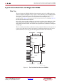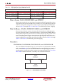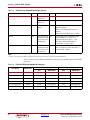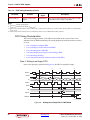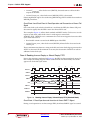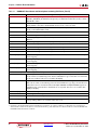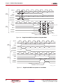
1
7 Series FPGAs Memory Resources User Guide UG473 (v1.11) November 12, 2014 The information disclosed to you hereunder (the “Materials”) is provided solely for the selection and use of Xilinx products. To the maximum extent permitted by applicable law: (1) Materials are made available "AS IS" and with all faults, Xilinx hereby DISCLAIMS ALL WARRANTIES AND CONDITIONS, EXPRESS, IMPLIED, OR STATUTORY, INCLUDING BUT NOT LIMITED TO WARRANTIES OF MERCHANTABILITY, NON-INFRINGEMENT, OR FITNESS FOR ANY PARTICULAR PURPOSE; and (2) Xilinx shall not be liable (whether in contract or tort, including negligence, or under any other theory of liability) for any loss or damage of any kind or nature related to, arising under, or in connection with, the Materials (including your use of the Materials), including for any direct, indirect, special, incidental, or consequential loss or damage (including loss of data, profits, goodwill, or any type of loss or damage suffered as a result of any action brought by a third party) even if such damage or loss was reasonably foreseeable or Xilinx had been advised of the possibility of the same. Xilinx assumes no obligation to correct any errors contained in the Materials or to notify you of updates to the Materials or to product specifications. You may not reproduce, modify, distribute, or publicly display the Materials without prior written consent. Certain products are subject to the terms and conditions of Xilinx’s limited warranty, please refer to Xilinx’s Terms of Sale which can be viewed at http://www.xilinx.com/legal.htm#tos; IP cores may be subject to warranty and support terms contained in a license issued to you by Xilinx. Xilinx products are not designed or intended to be fail-safe or for use in any application requiring fail-safe performance; you assume sole risk and liability for use of Xilinx products in such critical applications, please refer to Xilinx’s Terms of Sale which can be viewed at http://www.xilinx.com/legal.htm#tos. AUTOMOTIVE APPLICATIONS DISCLAIMER XILINX PRODUCTS ARE NOT DESIGNED OR INTENDED TO BE FAIL-SAFE, OR FOR USE IN ANY APPLICATION REQUIRING FAILSAFE PERFORMANCE, SUCH AS APPLICATIONS RELATED TO: (I) THE DEPLOYMENT OF AIRBAGS, (II) CONTROL OF A VEHICLE, UNLESS THERE IS A FAIL-SAFE OR REDUNDANCY FEATURE (WHICH DOES NOT INCLUDE USE OF SOFTWARE IN THE XILINX DEVICE TO IMPLEMENT THE REDUNDANCY) AND A WARNING SIGNAL UPON FAILURE TO THE OPERATOR, OR (III) USES THAT COULD LEAD TO DEATH OR PERSONAL INJURY. CUSTOMER ASSUMES THE SOLE RISK AND LIABILITY OF ANY USE OF XILINX PRODUCTS IN SUCH APPLICATIONS. © Copyright 2011–2014 Xilinx, Inc. Xilinx, the Xilinx logo, Artix, ISE, Kintex, Spartan, Virtex, Vivado, Zynq, and other designated brands included herein are trademarks of Xilinx in the United States and other countries. Revision History The following table shows the revision history for this document. Date Version Revision 03/01/2011 1.0 Initial Xilinx release. 03/28/2011 1.1 Updated disclaimer and copyright on page 2. Updated values in Table 2-1, descriptions in Table 2-3, and values in Table 2-4. Modified discussions in Almost Empty Flag, Full Flag, and Almost Full Flag sections. Updated values in Table 2-7 and Table 2-8. Revised Figure 2-6. Revised discussion of clock event 2 and clock event 4 on page 59. Updated Case 3: Reading from a Full FIFO including Figure 2-8. 04/14/2011 1.2 Added 7 Series FPGAs Block RAM and FIFO Differences from Previous FPGA Generations. Added Table 1-2: Block RAM Resources in 7 Series Devices. Clarified valid values for Read Width - READ_WIDTH_[A|B] and Write Width WRITE_WIDTH_[A|B] Updated the example in Block RAM Location Constraints. Updated parameter names in Table 1-18. Clarified the flag behavior in the Synchronous FIFO introduction. Revised the FIFO Almost Full/Empty Flag Offset Range section including adding Note 1 to Table 2-8, removing Equation 2-1 and revising Equation 2-2 to be the new Equation 2-1. Updated port connection instructions for WEBWE[7:0]. 10/18/2011 1.3 Added Stacked Silicon Interconnect. Added Artix-7 and Virtex-7 families to Table 1-2 and updated table notes. 11/18/2011 1.4 Updated second bullet in Changes from Virtex-6 FPGAs. 7 Series FPGAs Memory Resources www.xilinx.com UG473 (v1.11) November 12, 2014 Date Version Revision 01/30/2012 1.5 In Table 1-2, removed XC7A8, XC7A15, XC7A30T, and XC7A50T; updated number of 36 Kb block RAM blocks per column for XC7K420T and XC7VX550T; updated note 1 to say “GTP/GTX Quad.” Updated Simple Dual-Port Block RAM. 07/04/2012 1.6 Updated fifth and sixth bullets in Changes from Virtex-6 FPGAs. Added Virtex-7 devices to Table 1-2. Updated descriptions of RAMB36E1, RAMB18E1, and FIFO18E1 in Table 1-6. Updated description of WREN in Table 2-3. In Table 2-9, replaced TRCCK_RST/TRCKC_RST with TRREC_RST/TRREM_RST. 10/02/2012 1.7 Removed XC7A350T, XC7V1500T, and XC7VH290T from Table 1-2. 08/07/2013 1.8 Added three devices to Table 1-2. 10/02/2013 1.9 Update disclaimer and copyright on page 2. Updated Byte-Wide Write Enable. 01/30/2014 1.10 Updated the last bullet in Summary. Updated Figure 1-6 and Figure 3-2. 05/09/2014 1.10.1 11/12/2014 1.11 Typographical updates in Table 1-7 and Table 1-8. Added XC7A15T device to Table 1-2. UG473 (v1.11) November 12, 2014 www.xilinx.com 7 Series FPGAs Memory Resources 7 Series FPGAs Memory Resources www.xilinx.com UG473 (v1.11) November 12, 2014 Table of Contents Revision History . . . . . . . . . . . . . . . . . . . . . . . . . . . . . . . . . . . . . . . . . . . . . . . . . . . . . . . . . . . . . 2 Preface: About This Guide Guide Contents . . . . . . . . . . . . . . . . . . . . . . . . . . . . . . . . . . . . . . . . . . . . . . . . . . . . . . . . . . . . . . 9 7 Series FPGAs Block RAM and FIFO Differences from Previous FPGA Generations . . . . . . . . . . . . . . . . . . . . . . . . . . . . . . . . . . . . . . . . . . . . . . . . . . . . . . . . . 9 Changes from Virtex-6 FPGAs . . . . . . . . . . . . . . . . . . . . . . . . . . . . . . . . . . . . . . . . . . . . . . . 9 Changes from Spartan-6 FPGAs . . . . . . . . . . . . . . . . . . . . . . . . . . . . . . . . . . . . . . . . . . . . 10 Additional Support Resources . . . . . . . . . . . . . . . . . . . . . . . . . . . . . . . . . . . . . . . . . . . . . . . 10 Chapter 1: Block RAM Resources Summary . . . . . . . . . . . . . . . . . . . . . . . . . . . . . . . . . . . . . . . . . . . . . . . . . . . . . . . . . . . . . . . . . . . 11 Block RAM Introduction . . . . . . . . . . . . . . . . . . . . . . . . . . . . . . . . . . . . . . . . . . . . . . . . . . . . 13 Synchronous Dual-Port and Single-Port RAMs . . . . . . . . . . . . . . . . . . . . . . . . . . . . . . 15 Data Flow . . . . . . . . . . . . . . . . . . . . . . . . . . . . . . . . . . . . . . . . . . . . . . . . . . . . . . . . . . . . . . . Read Operation . . . . . . . . . . . . . . . . . . . . . . . . . . . . . . . . . . . . . . . . . . . . . . . . . . . . . . . . . . Write Operation . . . . . . . . . . . . . . . . . . . . . . . . . . . . . . . . . . . . . . . . . . . . . . . . . . . . . . . . . . Write Modes . . . . . . . . . . . . . . . . . . . . . . . . . . . . . . . . . . . . . . . . . . . . . . . . . . . . . . . . . . . . . WRITE_FIRST or Transparent Mode (Default) . . . . . . . . . . . . . . . . . . . . . . . . . . . . . . . . READ_FIRST or Read-Before-Write Mode . . . . . . . . . . . . . . . . . . . . . . . . . . . . . . . . . . . NO_CHANGE Mode . . . . . . . . . . . . . . . . . . . . . . . . . . . . . . . . . . . . . . . . . . . . . . . . . . . Conflict Avoidance . . . . . . . . . . . . . . . . . . . . . . . . . . . . . . . . . . . . . . . . . . . . . . . . . . . . . . . Asynchronous Clocking . . . . . . . . . . . . . . . . . . . . . . . . . . . . . . . . . . . . . . . . . . . . . . . . . Synchronous Clocking . . . . . . . . . . . . . . . . . . . . . . . . . . . . . . . . . . . . . . . . . . . . . . . . . . 15 16 16 16 17 17 17 18 18 18 Additional Block RAM Features in 7 Series Devices . . . . . . . . . . . . . . . . . . . . . . . . . 19 Optional Output Registers . . . . . . . . . . . . . . . . . . . . . . . . . . . . . . . . . . . . . . . . . . . . . . . . . Independent Read and Write Port Width Selection . . . . . . . . . . . . . . . . . . . . . . . . . . . . Simple Dual-Port Block RAM . . . . . . . . . . . . . . . . . . . . . . . . . . . . . . . . . . . . . . . . . . . . . . Cascadable Block RAM . . . . . . . . . . . . . . . . . . . . . . . . . . . . . . . . . . . . . . . . . . . . . . . . . . . . Byte-Wide Write Enable . . . . . . . . . . . . . . . . . . . . . . . . . . . . . . . . . . . . . . . . . . . . . . . . . . . Block RAM Error Correction Code . . . . . . . . . . . . . . . . . . . . . . . . . . . . . . . . . . . . . . . . . . Power Gating of Unused Block RAMs . . . . . . . . . . . . . . . . . . . . . . . . . . . . . . . . . . . . . . . 19 19 20 21 21 22 22 Block RAM Library Primitives . . . . . . . . . . . . . . . . . . . . . . . . . . . . . . . . . . . . . . . . . . . . . . 23 Block RAM Port Signals . . . . . . . . . . . . . . . . . . . . . . . . . . . . . . . . . . . . . . . . . . . . . . . . . . . . . 26 Clock - CLKARDCLK and CLKBWRCLK . . . . . . . . . . . . . . . . . . . . . . . . . . . . . . . . . . . . Enable - ENARDEN and ENBWREN . . . . . . . . . . . . . . . . . . . . . . . . . . . . . . . . . . . . . . . . Byte-Wide Write Enable - WEA and WEBWE . . . . . . . . . . . . . . . . . . . . . . . . . . . . . . . . . Register Enable - REGCEA, REGCE, and REGCEB . . . . . . . . . . . . . . . . . . . . . . . . . . . . Set/Reset . . . . . . . . . . . . . . . . . . . . . . . . . . . . . . . . . . . . . . . . . . . . . . . . . . . . . . . . . . . . . . . . RSTREGARSTREG, RSTREGB, RSTRAMARSTRAM, and RSTRAMB . . . . . . . . . . . . . . Address Bus - ADDRARDADDR and ADDRBWRADDR . . . . . . . . . . . . . . . . . . . . . . Data-In Buses - DIADI, DIPADIP, DIBDI, and DIPBDIP. . . . . . . . . . . . . . . . . . . . . . . . Data-Out Buses - DOADO, DOPADOP, DOBDO, and DOPBDOP . . . . . . . . . . . . . . . Cascade In . . . . . . . . . . . . . . . . . . . . . . . . . . . . . . . . . . . . . . . . . . . . . . . . . . . . . . . . . . . . . . . CASCADEINA, CASCADEINB, CASCADEOUTA, and CASCADEOUTB . . . . . . . . . . 7 Series FPGAs Memory Resources UG473 (v1.11) November 12, 2014 www.xilinx.com 26 26 26 27 27 27 27 29 29 29 29 Send Feedback 5 Inverting Control Pins . . . . . . . . . . . . . . . . . . . . . . . . . . . . . . . . . . . . . . . . . . . . . . . . . . . . . 30 GSR . . . . . . . . . . . . . . . . . . . . . . . . . . . . . . . . . . . . . . . . . . . . . . . . . . . . . . . . . . . . . . . . . . . . . 30 Unused Inputs . . . . . . . . . . . . . . . . . . . . . . . . . . . . . . . . . . . . . . . . . . . . . . . . . . . . . . . . . . . 30 Block RAM Address Mapping . . . . . . . . . . . . . . . . . . . . . . . . . . . . . . . . . . . . . . . . . . . . . . . 30 Block RAM Attributes . . . . . . . . . . . . . . . . . . . . . . . . . . . . . . . . . . . . . . . . . . . . . . . . . . . . . . 31 Content Initialization - INIT_xx . . . . . . . . . . . . . . . . . . . . . . . . . . . . . . . . . . . . . . . . . . . . . Content Initialization - INITP_xx . . . . . . . . . . . . . . . . . . . . . . . . . . . . . . . . . . . . . . . . . . . Output Latches Initialization - INIT (INIT_A or INIT_B) . . . . . . . . . . . . . . . . . . . . . . . Output Latches/Registers Synchronous Set/Reset (SRVAL_[A|B]) . . . . . . . . . . . . . . Reset or CE Priority - RSTREG_PRIORITY_[A|B] . . . . . . . . . . . . . . . . . . . . . . . . . . . . . Optional Output Register On/Off Switch - DO[A|B]_REG . . . . . . . . . . . . . . . . . . . . . Extended Mode Address Determinant - RAM_EXTENSION_[A|B] . . . . . . . . . . . . . Read Width - READ_WIDTH_[A|B] . . . . . . . . . . . . . . . . . . . . . . . . . . . . . . . . . . . . . . . . Write Width - WRITE_WIDTH_[A|B] . . . . . . . . . . . . . . . . . . . . . . . . . . . . . . . . . . . . . . . Mode Selection - RAM_MODE . . . . . . . . . . . . . . . . . . . . . . . . . . . . . . . . . . . . . . . . . . . . . Write Mode - WRITE_MODE_[A|B] . . . . . . . . . . . . . . . . . . . . . . . . . . . . . . . . . . . . . . . . RDADDR_COLLISION_HWCONFIG . . . . . . . . . . . . . . . . . . . . . . . . . . . . . . . . . . . . . . . SIM_COLLISION_CHECK . . . . . . . . . . . . . . . . . . . . . . . . . . . . . . . . . . . . . . . . . . . . . . . . . INIT_FILE . . . . . . . . . . . . . . . . . . . . . . . . . . . . . . . . . . . . . . . . . . . . . . . . . . . . . . . . . . . . . . . SIM_DEVICE . . . . . . . . . . . . . . . . . . . . . . . . . . . . . . . . . . . . . . . . . . . . . . . . . . . . . . . . . . . . 31 32 32 32 33 33 33 33 33 34 34 34 34 34 34 Block RAM Location Constraints . . . . . . . . . . . . . . . . . . . . . . . . . . . . . . . . . . . . . . . . . . . . 34 Block RAM Initialization in VHDL or Verilog Code . . . . . . . . . . . . . . . . . . . . . . . . . 35 Additional RAMB18E1 and RAMB36E1 Primitive Design Considerations . . . . 35 Optional Output Registers . . . . . . . . . . . . . . . . . . . . . . . . . . . . . . . . . . . . . . . . . . . . . . . . . Independent Read and Write Port Width . . . . . . . . . . . . . . . . . . . . . . . . . . . . . . . . . . . . RAMB18E1 and RAMB36E1 Port Mapping Design Rules . . . . . . . . . . . . . . . . . . . . . . . Cascadable Block RAM . . . . . . . . . . . . . . . . . . . . . . . . . . . . . . . . . . . . . . . . . . . . . . . . . . . . Byte-Wide Write Enable . . . . . . . . . . . . . . . . . . . . . . . . . . . . . . . . . . . . . . . . . . . . . . . . . . . 35 35 36 36 37 Block RAM Applications . . . . . . . . . . . . . . . . . . . . . . . . . . . . . . . . . . . . . . . . . . . . . . . . . . . . 37 Creating Larger RAM Structures . . . . . . . . . . . . . . . . . . . . . . . . . . . . . . . . . . . . . . . . . . . . 37 Block RAM RSTREG in Register Mode . . . . . . . . . . . . . . . . . . . . . . . . . . . . . . . . . . . . . . 37 Block RAM Timing Model . . . . . . . . . . . . . . . . . . . . . . . . . . . . . . . . . . . . . . . . . . . . . . . . . . 39 Block RAM Timing Parameters . . . . . . . . . . . . . . . . . . . . . . . . . . . . . . . . . . . . . . . . . . . . . Block RAM Timing Characteristics . . . . . . . . . . . . . . . . . . . . . . . . . . . . . . . . . . . . . . . . . . Clock Event 1 . . . . . . . . . . . . . . . . . . . . . . . . . . . . . . . . . . . . . . . . . . . . . . . . . . . . . . . . . Clock Event 2 . . . . . . . . . . . . . . . . . . . . . . . . . . . . . . . . . . . . . . . . . . . . . . . . . . . . . . . . . Clock Event 4 . . . . . . . . . . . . . . . . . . . . . . . . . . . . . . . . . . . . . . . . . . . . . . . . . . . . . . . . . Clock Event 5 . . . . . . . . . . . . . . . . . . . . . . . . . . . . . . . . . . . . . . . . . . . . . . . . . . . . . . . . . Block RAM Timing Model . . . . . . . . . . . . . . . . . . . . . . . . . . . . . . . . . . . . . . . . . . . . . . . . . 39 40 41 41 41 42 42 Stacked Silicon Interconnect . . . . . . . . . . . . . . . . . . . . . . . . . . . . . . . . . . . . . . . . . . . . . . . . 43 Chapter 2: Built-in FIFO Support Overview . . . . . . . . . . . . . . . . . . . . . . . . . . . . . . . . . . . . . . . . . . . . . . . . . . . . . . . . . . . . . . . . . . . 45 Dual-Clock FIFO . . . . . . . . . . . . . . . . . . . . . . . . . . . . . . . . . . . . . . . . . . . . . . . . . . . . . . . . . . . . 45 Synchronous FIFO . . . . . . . . . . . . . . . . . . . . . . . . . . . . . . . . . . . . . . . . . . . . . . . . . . . . . . . . . . 46 Synchronous FIFO Implementations . . . . . . . . . . . . . . . . . . . . . . . . . . . . . . . . . . . . . . . . 47 FIFO Architecture: a Top-Level View . . . . . . . . . . . . . . . . . . . . . . . . . . . . . . . . . . . . . . . . 48 FIFO Primitives . . . . . . . . . . . . . . . . . . . . . . . . . . . . . . . . . . . . . . . . . . . . . . . . . . . . . . . . . . . . . 48 FIFO Port Descriptions . . . . . . . . . . . . . . . . . . . . . . . . . . . . . . . . . . . . . . . . . . . . . . . . . . . . . . 49 6 Send Feedback www.xilinx.com 7 Series FPGAs Memory Resources UG473 (v1.11) November 12, 2014 FIFO Operations . . . . . . . . . . . . . . . . . . . . . . . . . . . . . . . . . . . . . . . . . . . . . . . . . . . . . . . . . . . . 51 Reset . . . . . . . . . . . . . . . . . . . . . . . . . . . . . . . . . . . . . . . . . . . . . . . . . . . . . . . . . . . . . . . . . . . . Operating Mode . . . . . . . . . . . . . . . . . . . . . . . . . . . . . . . . . . . . . . . . . . . . . . . . . . . . . . . . . . Standard Mode . . . . . . . . . . . . . . . . . . . . . . . . . . . . . . . . . . . . . . . . . . . . . . . . . . . . . . . . First Word Fall Through (FWFT) Mode . . . . . . . . . . . . . . . . . . . . . . . . . . . . . . . . . . . . . Status Flags . . . . . . . . . . . . . . . . . . . . . . . . . . . . . . . . . . . . . . . . . . . . . . . . . . . . . . . . . . . . . . Empty Flag . . . . . . . . . . . . . . . . . . . . . . . . . . . . . . . . . . . . . . . . . . . . . . . . . . . . . . . . . . . Almost Empty Flag . . . . . . . . . . . . . . . . . . . . . . . . . . . . . . . . . . . . . . . . . . . . . . . . . . . . . Read Error Flag . . . . . . . . . . . . . . . . . . . . . . . . . . . . . . . . . . . . . . . . . . . . . . . . . . . . . . . . Full Flag . . . . . . . . . . . . . . . . . . . . . . . . . . . . . . . . . . . . . . . . . . . . . . . . . . . . . . . . . . . . . Write Error Flag . . . . . . . . . . . . . . . . . . . . . . . . . . . . . . . . . . . . . . . . . . . . . . . . . . . . . . . Almost Full Flag . . . . . . . . . . . . . . . . . . . . . . . . . . . . . . . . . . . . . . . . . . . . . . . . . . . . . . . 51 51 51 51 51 52 52 52 53 53 53 FIFO Attributes . . . . . . . . . . . . . . . . . . . . . . . . . . . . . . . . . . . . . . . . . . . . . . . . . . . . . . . . . . . . . 53 FIFO Almost Full/Empty Flag Offset Range . . . . . . . . . . . . . . . . . . . . . . . . . . . . . . . . . . 55 FIFO VHDL and Verilog Templates . . . . . . . . . . . . . . . . . . . . . . . . . . . . . . . . . . . . . . . . . 56 FIFO Timing Models and Parameters . . . . . . . . . . . . . . . . . . . . . . . . . . . . . . . . . . . . . . . . 56 FIFO Timing Characteristics . . . . . . . . . . . . . . . . . . . . . . . . . . . . . . . . . . . . . . . . . . . . . . . . Case 1: Writing to an Empty FIFO . . . . . . . . . . . . . . . . . . . . . . . . . . . . . . . . . . . . . . . . . Case 2: Writing to a Full or Almost Full FIFO . . . . . . . . . . . . . . . . . . . . . . . . . . . . . . . . . Case 3: Reading from a Full FIFO . . . . . . . . . . . . . . . . . . . . . . . . . . . . . . . . . . . . . . . . . . Case 4: Reading from an Empty or Almost Empty FIFO . . . . . . . . . . . . . . . . . . . . . . . . Case 5: Resetting All Flags . . . . . . . . . . . . . . . . . . . . . . . . . . . . . . . . . . . . . . . . . . . . . . . Case 6: Simultaneous Read and Write for Dual-Clock FIFO . . . . . . . . . . . . . . . . . . . . . . 58 58 60 61 62 64 64 FIFO Applications . . . . . . . . . . . . . . . . . . . . . . . . . . . . . . . . . . . . . . . . . . . . . . . . . . . . . . . . . . 64 Cascading FIFOs to Increase Depth . . . . . . . . . . . . . . . . . . . . . . . . . . . . . . . . . . . . . . . . . 64 Connecting FIFOs in Parallel to Increase Width . . . . . . . . . . . . . . . . . . . . . . . . . . . . . . . 66 Legal Block RAM and FIFO Combinations . . . . . . . . . . . . . . . . . . . . . . . . . . . . . . . . . . 67 Chapter 3: Built-in Error Correction Overview . . . . . . . . . . . . . . . . . . . . . . . . . . . . . . . . . . . . . . . . . . . . . . . . . . . . . . . . . . . . . . . . . . . 69 ECC Modes . . . . . . . . . . . . . . . . . . . . . . . . . . . . . . . . . . . . . . . . . . . . . . . . . . . . . . . . . . . . . . . . . 70 Top-Level View of the Block RAM ECC Architecture . . . . . . . . . . . . . . . . . . . . . . . . 71 Block RAM and FIFO ECC Primitive . . . . . . . . . . . . . . . . . . . . . . . . . . . . . . . . . . . . . . . . 72 Block RAM and FIFO ECC Port Descriptions . . . . . . . . . . . . . . . . . . . . . . . . . . . . . . . . 73 Block RAM and FIFO ECC Attributes . . . . . . . . . . . . . . . . . . . . . . . . . . . . . . . . . . . . . . . 76 ECC Modes of Operation . . . . . . . . . . . . . . . . . . . . . . . . . . . . . . . . . . . . . . . . . . . . . . . . . . . . 76 Standard ECC . . . . . . . . . . . . . . . . . . . . . . . . . . . . . . . . . . . . . . . . . . . . . . . . . . . . . . . . . . . . Set by Attributes . . . . . . . . . . . . . . . . . . . . . . . . . . . . . . . . . . . . . . . . . . . . . . . . . . . . . . . Standard ECC Write . . . . . . . . . . . . . . . . . . . . . . . . . . . . . . . . . . . . . . . . . . . . . . . . . . . . Standard ECC Read . . . . . . . . . . . . . . . . . . . . . . . . . . . . . . . . . . . . . . . . . . . . . . . . . . . . ECC Encode Only . . . . . . . . . . . . . . . . . . . . . . . . . . . . . . . . . . . . . . . . . . . . . . . . . . . . . . . . Set by Attributes . . . . . . . . . . . . . . . . . . . . . . . . . . . . . . . . . . . . . . . . . . . . . . . . . . . . . . . ECC Encode-Only Write . . . . . . . . . . . . . . . . . . . . . . . . . . . . . . . . . . . . . . . . . . . . . . . . . ECC Encode-Only Read . . . . . . . . . . . . . . . . . . . . . . . . . . . . . . . . . . . . . . . . . . . . . . . . . ECC Decode Only . . . . . . . . . . . . . . . . . . . . . . . . . . . . . . . . . . . . . . . . . . . . . . . . . . . . . . . . Set by Attributes . . . . . . . . . . . . . . . . . . . . . . . . . . . . . . . . . . . . . . . . . . . . . . . . . . . . . . . Using ECC Decode Only to Inject Single-Bit Error . . . . . . . . . . . . . . . . . . . . . . . . . . . . . Using the ECC Decode-Only to Inject Double-Bit Error . . . . . . . . . . . . . . . . . . . . . . . . . 79 79 80 80 80 80 80 81 81 81 81 81 ECC Timing Characteristics . . . . . . . . . . . . . . . . . . . . . . . . . . . . . . . . . . . . . . . . . . . . . . . . . 82 Standard ECC Write Timing . . . . . . . . . . . . . . . . . . . . . . . . . . . . . . . . . . . . . . . . . . . . . . . 82 7 Series FPGAs Memory Resources UG473 (v1.11) November 12, 2014 www.xilinx.com Send Feedback 7 Standard ECC Read Timing . . . . . . . . . . . . . . . . . . . . . . . . . . . . . . . . . . . . . . . . . . . . . . . . DO_REG = 0 . . . . . . . . . . . . . . . . . . . . . . . . . . . . . . . . . . . . . . . . . . . . . . . . . . . . . . . . . . DO_REG = 1 . . . . . . . . . . . . . . . . . . . . . . . . . . . . . . . . . . . . . . . . . . . . . . . . . . . . . . . . . . Encode-Only ECC Write Timing . . . . . . . . . . . . . . . . . . . . . . . . . . . . . . . . . . . . . . . . . . . . Encode-Only ECC Read Timing . . . . . . . . . . . . . . . . . . . . . . . . . . . . . . . . . . . . . . . . . . . . Decode-Only ECC Write Timing . . . . . . . . . . . . . . . . . . . . . . . . . . . . . . . . . . . . . . . . . . . . Decode-Only ECC Read Timing . . . . . . . . . . . . . . . . . . . . . . . . . . . . . . . . . . . . . . . . . . . . 82 82 82 83 83 83 83 Block RAM ECC Mode Timing Parameters . . . . . . . . . . . . . . . . . . . . . . . . . . . . . . . . . . 84 Creating 8 Parity Bits for a 64-bit Word . . . . . . . . . . . . . . . . . . . . . . . . . . . . . . . . . . . . . . 85 Block RAM ECC VHDL and Verilog Templates . . . . . . . . . . . . . . . . . . . . . . . . . . . . . 85 8 Send Feedback www.xilinx.com 7 Series FPGAs Memory Resources UG473 (v1.11) November 12, 2014 Preface About This Guide Xilinx® 7 series FPGAs include three FPGA families that are all designed for lowest power to enable a common design to scale across families for optimal power, performance, and cost. The Artix®-7 family is optimized for lowest cost and absolute power for the highest volume applications. The Virtex®-7 family is optimized for highest system performance and capacity. The Kintex®-7 family is an innovative class of FPGAs optimized for the best price-performance. This guide serves as a technical reference describing the 7 series FPGAs block RAMs. Block RAMs are used for efficient data storage or buffering, for high-performance state machines or FIFO buffers, for large shift registers, large look-up tables, or ROMs. This 7 series FPGAs memory resources user guide, part of an overall set of documentation on the 7 series FPGAs, is available on the Xilinx website at: www.xilinx.com/support/documentation/7_series Guide Contents This manual contains these chapters: • Chapter 1, Block RAM Resources • Chapter 2, Built-in FIFO Support • Chapter 3, Built-in Error Correction 7 Series FPGAs Block RAM and FIFO Differences from Previous FPGA Generations Changes from Virtex-6 FPGAs • The rules for conflict avoidance and address collision are relaxed. • In SDP mode, the WRITE_FIRST mode is automatically mapped to the NO_CHANGE mode for power savings. • The block RAM content initialization and readback behavior is changed due to a new power gating implementation. • The new external power supply VCCBRAM is used to power the block RAM memory cells. • The FIFO reset requirements are simplified in 7 series FPGAs. The FIFO reset assertion is now synchronized to the read and write clocks. However, the reset deassertion is still asynchronous. • Overall, the FIFO flag latencies are different than in Virtex-6 FPGAs (see Table 2-4). 7 Series FPGAs Memory Resources UG473 (v1.11) November 12, 2014 www.xilinx.com Send Feedback 9 Preface: About This Guide • The ALMOST_FULL_OFFSET equation for the 7 series FPGAs is changed in the case where the RDCLK is different from the WRCLK. In this case, the ALMOST_EMPTY_OFFSET equation is removed because in all cases it follows the values in Table 2-8. Changes from Spartan-6 FPGAs • Similar to the Virtex-6 family, the 7 series FPGAs support both 36 Kb and 18 Kb block RAM configurations (native 36 Kb/18 Kb versus the 18 Kb/9 Kb of the Spartan®-6 FPGAs). • Many key features already available in the Virtex-6 family but not in the Spartan-6 family are included in the 7 series FPGAs implementation: • Dedicated integrated FIFO • Error correction (ECC) • Direct cascade of block RAM • Independent reset control of output latches and registers • Asynchronous set/reset of data outputs Additional Support Resources To find additional documentation, see the Xilinx website at: www.xilinx.com/support/documentation/index To search the Answer Database of silicon, software, and IP questions and answers, or to create a technical support WebCase, see the Xilinx website at: www.xilinx.com/support 10 Send Feedback www.xilinx.com 7 Series FPGAs Memory Resources UG473 (v1.11) November 12, 2014 Chapter 1 Block RAM Resources Summary The block RAM in Xilinx® 7 series FPGAs stores up to 36 Kbits of data and can be configured as either two independent 18 Kb RAMs, or one 36 Kb RAM. Each 36 Kb block RAM can be configured as a 64K x 1 (when cascaded with an adjacent 36 Kb block RAM), 32K x 1, 16K x 2, 8K x 4, 4K x 9, 2K x 18, 1K x 36, or 512 x 72 in simple dual-port mode. Each 18 Kb block RAM can be configured as a 16K x 1, 8K x2 , 4K x 4, 2K x 9, 1K x 18 or 512 x 36 in simple dual-port mode. Similar to the Virtex®-6 FPGA block RAMs, Write and Read are synchronous operations; the two ports are symmetrical and totally independent, sharing only the stored data. Each port can be configured in one of the available widths, independent of the other port. In addition, the read port width can be different from the write port width for each port. The memory content can be initialized or cleared by the configuration bitstream. During a write operation the memory can be set to have the data output remain unchanged, reflect the new data being written or the previous data now being overwritten. The 7 series FPGAs block RAM features include: • Per block memory storage capability where each block RAM can store up to 36 Kbits of data. • Support of two independent 18Kb blocks, or a single 36Kb block RAM. • Each 36Kb block RAM can be set to simple dual-port (SDP) mode, doubling data width of the block RAM to 72 bits. The 18Kb block RAM can also be set to simple dual-port mode, doubling data width to 36 bits. Simple dual-port mode is defined as having one read-only port and one write-only port with independent clocks. • The simple dual-port RAM supports a fixed width data port setting on one side with a variable data port width setting on the other side. • Two adjacent block RAMs can be combined to one deeper 64K x 1 memory without any external logic. • One 64-bit Error Correction Coding block is provided per 36 Kb block RAM or 36 Kb FIFO. Separate encode/decode functionality is available. Capability to inject errors in ECC mode. • Synchronous Set/Reset of the outputs to an initial value is available for both the latch and register modes of the block RAM output. • Separate synchronous Set/Reset pins to independently control the Set/Reset of the optional output registers and output latch stages in the block RAM. • An attribute to configure the block RAM as a synchronous FIFO to eliminate flag latency uncertainty. • The FULL flag in 7 series FPGAs is asserted without any latency. 7 Series FPGAs Memory Resources UG473 (v1.11) November 12, 2014 www.xilinx.com Send Feedback 11 Chapter 1: Block RAM Resources • 18, 36, or 72-bit wide block RAM ports can have an individual write enable per byte. This feature is popular for interfacing to a microprocessor. • Each block RAM contains optional address sequencing and control circuitry to operate as a built-in dual-clock FIFO memory. In the 7 series architecture, the block RAM can be configured as an 18 Kb or 36 Kb FIFO. • All inputs are registered with the port clock and have a setup-to-clock timing specification. • All outputs have a read function or a read-during-write function, depending on the state of the write enable (WE) pin. The outputs are available after the clock-to-out timing interval. The read-during-write outputs have one of three operating modes: WRITE_FIRST, READ_FIRST, and NO_CHANGE. • A write operation requires one clock edge. • A read operation requires one clock edge. • All output ports are latched or registered (optional). The state of the output port does not change until the port executes another read or write operation. The default block RAM output is latch mode. • The output datapath has an optional internal pipeline register. Using the register mode is strongly recommended. This allows a higher clock rate; however, it adds a clock cycle latency of one. The 7 series FPGAs block RAM usage rules include: 12 • The synchronous set/reset (RSTRAM) ports cannot be used when the ECC decoder is enabled (EN_ECC_READ = TRUE). • The block RAM synchronous output registers (optional) are set or reset (SRVAL) with RSTREG when DO_REG = 1. The RSTREG_PRIORITY attribute determines if RSTREG has priority over REGCE. The synchronous output latches are set or reset (SRVAL) with RSTRAM when DO_REG is 0 or 1. • The setup time of the block RAM address and write enable pins must not be violated. Violating the address setup time (even if write enable is Low) can corrupt the data contents of the block RAM. • The block RAM register mode RSTREG requires REGCE = 1 to reset the output DO register value; if the RSTREG_PRIORITY is set to REGCE. The block RAM array data output latch does not get reset in this mode. The block RAM latch mode RSTRAM requires the block RAM enable, EN = 1, to reset the output DO latch value. • There are two block RAM primitives: RAMB36E1 and RAMB18E1. The RAM_MODE attribute determines the mode of the block RAM, either SDP mode or true dual-port (TDP) mode. • Different read and write port width choices are available when using specific block RAM primitives. The parity bits are only available for the x9, x18, and x36 port widths. The parity bits should not be used when the read width is x1, x2, or x4. If the read width is x1, x2 or x4, the effective write width is x1, x2, x4, x8, x16, or x32. Similarly, when a write width is x1, x2, or x4, the actual available read width is x1, x2, x4, x8, x16, or x32 even though the primitive attribute is set to 1, 2, 4, 9, 18, or 36, respectively. Table 1-1 shows some possible scenarios. Send Feedback www.xilinx.com 7 Series FPGAs Memory Resources UG473 (v1.11) November 12, 2014 Block RAM Introduction Table 1-1: Parity Use Scenarios Settings Primitive Effective Read Width Effective Write Width Read Width Write Width RAMB18E1 1, 2, or 4 9 or 18 Same as setting 8 or 16 RAMB18E1 9 or 18 1, 2, or 4 8 or 16 Same as setting RAMB18E1 1, 2, or 4 1, 2, or 4 Same as setting Same as setting RAMB18E1 9 or 18 9 or 18 Same as setting Same as setting RAMB36E1 1, 2, or 4 9, 18, or 36 Same as setting 8, 16, or 32 RAMB36E1 9, 18, or 36 1, 2, or 4 8, 16, or 32 Same as setting RAMB36E1 1, 2, or 4 1, 2, or 4 Same as setting Same as setting RAMB36E1 9, 18, or 36 9, 18, or 36 Same as setting Same as setting Notes: 1. Do not use parity bits DIP/DOP when one port width is less than 9 and another port width is 9 or greater. • The A15 pin in the RAMB36E1 should be used for cascading only. In all other cases, A15 should be left unconnected or tied High. • An asynchronous assertion or deassertion of the EN signal caused by an asynchronous reset can violate the setup/hold time of the EN signal. In this case, the first read or write operation does not yield the expected result. If an asynchronous assertion or deassertion of EN cannot be avoided, keep EN deasserted during asynchronous RESET assertion and deassertion or insert a read or write cycle after EN has been asserted before a valid data cycle occurs. If the PLL or MMCM LOCKED signal is lost, or a free running clock stops, immediately deassert EN. Block RAM Introduction In addition to distributed RAM and high-speed SelectIO™ memory interfaces, 7 series devices feature a large number of 36 Kb block RAMs. Each 36 Kb block RAM contains two independently controlled 18 Kb RAMs. Block RAMs are placed in columns, and the total number of block RAM resources is listed in Table 1-2 by the 7 series device. The 36 Kb blocks are cascadable to enable a deeper and wider memory implementation, with a minimal timing penalty. Table 1-2: Block RAM Resources in 7 Series Devices Device Total 36 Kb Block RAM Blocks per Device Number of 36 Kb Block RAM Columns per Device Number of 36 Kb Block RAM Blocks per Column XC7A15T 25 3 30(1) (2)(4) XC7A35T 50 3 30(1) (2)(4) XC7A50T 75 3 30(1) (2) XC7A75T 105 4 40(1) (2)(4) XC7A100T 135 4 40 (1) (2) XC7A200T 365 9 50 (2) (3) 7 Series FPGAs Memory Resources UG473 (v1.11) November 12, 2014 www.xilinx.com Send Feedback 13 Chapter 1: Block RAM Resources Table 1-2: Block RAM Resources in 7 Series Devices (Cont’d) Device Total 36 Kb Block RAM Blocks per Device Number of 36 Kb Block RAM Columns per Device Number of 36 Kb Block RAM Blocks per Column XC7K70T 135 4 40 (1) (2) XC7K160T 325 7 50 (1) (2) XC7K325T 445 7 70 (1) (2) XC7K355T 715 12 60 (2) XC7K410T 795 12 70 (1) (2) XC7K420T 835 12 80 (2) (4) XC7K480T 955 12 80 (2) XC7V585T 795 9 90 (2) XC7V2000T 1,292 11 120 (2) (5)(6) XC7VX330T 750 11 70 (7) XC7VX415T 880 15 60 (7) XC7VX485T 1,030 15 70 (2) XC7VX550T 1,180 15 100 (4) (7) XC7VX690T 1,470 15 100 (7) XC7VX980T 1,500 17 90 (7) XC7VX1140T 1,880 16 120 (5) (6)(7) XC7VH580T 940 16 60 (7) XC7VH870T 1,410 16 90 (7) Notes: 1. The right side column contains GTP/GTX Quads that displace ten block RAM blocks in that column per GTP/GTX Quad. 2. The column containing Gen1/Gen2 interface blocks for PCI Express® displaces five block RAM blocks per interface block for PCI Express. Block RAM blocks cannot be cascaded across interface blocks for PCI Express. 3. The four center block RAM columns contain GTP Quads that displace ten block RAM blocks in those columns per GTP Quad. 4. The total block RAM block count is limited by software. 5. The block RAM column on the left side of the device has two less block RAM blocks per super logic region (SLR). 6. There are thirty 36 Kb block RAM blocks per column in each SLR. 7. The column containing Gen3 interface blocks for PCI Express displaces ten block RAM blocks per interface block for PCI Express. Block RAM blocks cannot be cascaded across interface blocks for PCI Express. Embedded dual- or single-port RAM modules, ROM modules, synchronous FIFOs, and data width converters are implemented using the Xilinx CORE Generator™ block memory modules. Dual-clock FIFOs can be generated using the CORE Generator FIFO Generator module. The synchronous or asynchronous (dual-clock) FIFO implementation does not require additional CLB resources for the FIFO control logic because it uses dedicated hardware resources. 14 Send Feedback www.xilinx.com 7 Series FPGAs Memory Resources UG473 (v1.11) November 12, 2014 Synchronous Dual-Port and Single-Port RAMs Synchronous Dual-Port and Single-Port RAMs Data Flow The true dual-port 36 Kb block RAM dual-port memories consist of a 36 Kb storage area and two completely independent access ports, A and B. Similarly, each 18 Kb block RAM dual-port memory consists of an 18 Kb storage area and two completely independent access ports, A and B. The structure is fully symmetrical, and both ports are interchangeable. Figure 1-1 illustrates the true dual-port data flow of a RAMB36. Table 1-3 lists the port functions and descriptions. Data can be written to either or both ports and can be read from either or both ports. Each write operation is synchronous, each port has its own address, data in, data out, clock, clock enable, and write enable. The read and write operations are synchronous and require a clock edge. There is no dedicated monitor to arbitrate the effect of identical addresses on both ports. It is up to you to time the two clocks appropriately. Conflicting simultaneous writes to the same location never cause any physical damage but can result in data uncertainty. X-Ref Target - Figure 1-1 CASCADEOUTA CASCADEOUTB 36-Kbit Block RAM 32 4 16 4 DIA DIPA Port A ADDRA WEA ENA RSTREGA RSTRAMA CLKA REGCEA 32 4 16 4 DOA DOPA 32 4 36 Kb Memory Array DIB DIPB ADDRB WEB Port B ENB RSTREGB RSTRAMB DOB 32 DOPB 4 CLKB REGCEB CASCADEINA CASCADEINB UG473_c1_01_052610 Figure 1-1: 7 Series FPGAs Memory Resources UG473 (v1.11) November 12, 2014 True Dual-Port Data Flows for a RAMB36 www.xilinx.com Send Feedback 15 Chapter 1: Block RAM Resources Table 1-3: True Dual-Port Functions and Descriptions Port Function Description DI[A|B] Data input bus. DIP[A|B](1) Data input parity bus. Can be used for additional data inputs. ADDR[A|B] Address bus. WE[A|B] Byte-wide write enable. EN[A|B] When inactive no data is written to the block RAM and the output bus remains in its previous state. RSTREG[A|B] Synchronous Set/Reset the output registers (DO_REG = 1). The RSTREG_PRIORITY attribute determines the priority over REGCE. RSTRAM[A|B] Synchronous Set/Reset the output data latches. CLK[A|B] Clock input. DO[A|B] Data output bus. DOP[A|B](1) Data output parity bus. Can be used for additional data outputs. REGCE[A|B] Output Register clock enable. CASCADEIN[A|B] Cascade input for 64K x 1 mode. CASCADEOUT[A|B] Cascade output for 64K x 1 mode. Notes: 1. The Data-In Buses - DIADI, DIPADIP, DIBDI, and DIPBDIP section has more information on data parity pins. 2. Block RAM primitive port names can be different from the port function names. Read Operation In latch mode, the read operation uses one clock edge. The read address is registered on the read port, and the stored data is loaded into the output latches after the RAM access time. When using the output register, the read operation takes one extra latency cycle. Write Operation A write operation is a single clock-edge operation. The write address is registered on the write port, and the data input is stored in memory. Write Modes Three settings of the write mode determines the behavior of the data available on the output latches after a write clock edge: WRITE_FIRST, READ_FIRST, and NO_CHANGE. Write mode selection is set by configuration. The Write mode attribute can be individually selected for each port. The default mode is WRITE_FIRST. WRITE_FIRST outputs the newly written data onto the output bus. READ_FIRST outputs the previously stored data while new data is being written. NO_CHANGE maintains the output previously generated by a read operation. 16 Send Feedback www.xilinx.com 7 Series FPGAs Memory Resources UG473 (v1.11) November 12, 2014 Synchronous Dual-Port and Single-Port RAMs WRITE_FIRST or Transparent Mode (Default) In WRITE_FIRST mode, the input data is simultaneously written into memory and stored in the data output (transparent write), as shown in Figure 1-2. These waveforms correspond to latch mode when the optional output pipeline register is not used. X-Ref Target - Figure 1-2 CLK WE DI XXXX ADDR DO aa 0000 1111 2222 bb cc MEM(aa) 1111 XXXX dd 2222 MEM(dd) EN Disabled Read Write MEM(bb)=1111 Write MEM(cc)=2222 Read UG473_c1_02_052610 Figure 1-2: WRITE_FIRST Mode Waveforms READ_FIRST or Read-Before-Write Mode In READ_FIRST mode, data previously stored at the write address appears on the output latches, while the input data is being stored in memory (read before write). The waveforms in Figure 1-3 correspond to latch mode when the optional output pipeline register is not used. X-Ref Target - Figure 1-3 CLK WE DI XXXX ADDR DO aa 0000 MEM(aa) 1111 2222 bb cc old MEM(bb) XXXX dd old MEM(cc) MEM(dd) EN Disabled Read Write MEM(bb)=1111 Write MEM(cc)=2222 Read UG473_c1_03_052610 Figure 1-3: READ_FIRST Mode Waveforms NO_CHANGE Mode In NO_CHANGE mode, the output latches remain unchanged during a write operation. As shown in Figure 1-4, data output remains the last read data and is unaffected by a write operation on the same port. These waveforms correspond to latch mode when the optional 7 Series FPGAs Memory Resources UG473 (v1.11) November 12, 2014 www.xilinx.com Send Feedback 17 Chapter 1: Block RAM Resources output pipeline register is not used. This mode is the most power efficient. This mode is not available in the SDP mode because it is identical in behavior to WRITE_FIRST mode. X-Ref Target - Figure 1-4 CLK WE DI XXXX ADDR DO aa 0000 1111 2222 bb cc MEM(aa) XXXX dd MEM(dd) EN Disable Read Write MEM(bb)=1111 Write MEM(cc)=2222 Read UG473_c1_04_052610 Figure 1-4: NO_CHANGE Mode Waveforms Conflict Avoidance The 7 series FPGAs block RAM is a true dual-port RAM where both ports can access any memory location at any time. When accessing the same memory location from both ports, you must, however, observe certain restrictions. There are two fundamentally different situations: The two ports either have a common clock (synchronous clocking), or the clock frequency and phase is different for the two ports (asynchronous clocking). Asynchronous Clocking Asynchronous clocking is the more general case, where the active edges of both clocks do not occur simultaneously: • There are no timing restrictions when both ports perform a read operation. • When one port performs a write operation, the other port must not read or write access the same memory location. Therefore, the READ_FIRST mode should be avoided in true asynchronous applications, because there is no guarantee that the old data will be read (in both TDP and SDP modes). The WRITE_FIRST mode is the recommended mode when asynchronous clocks might cause simultaneous read/write operations on the same port address. The simulation model produces an error if this condition is violated. If this restriction is ignored, a read or write operation produces unpredictable results. There is, however, no risk of physical damage to the device. If a read and write operation is performed, then the write stores valid data at the write location. Synchronous Clocking Synchronous clocking is the special case, where the active edges of both port clocks occur simultaneously: 18 • Synchronous clocking is defined as both clock input pins being driven by the same clock. • There are no timing restrictions when both ports perform a read operation. Send Feedback www.xilinx.com 7 Series FPGAs Memory Resources UG473 (v1.11) November 12, 2014 Additional Block RAM Features in 7 Series Devices • When one port performs a write operation, the other port must not write into the same location, unless both ports write identical data. • When one port performs a write operation, the write operation succeeds; the other port can reliably read data from the same location if the write port is in READ_FIRST mode. DATA_OUT on both ports then reflects the previously stored data. If the write port is in either WRITE_FIRST or in NO_CHANGE mode, then the DATA_OUT on the read port would become invalid (unreliable). The mode setting of the read-port does not affect this operation. Additional Block RAM Features in 7 Series Devices Optional Output Registers The optional output registers improve design performance by eliminating routing delay to the CLB flip-flops for pipelined operation. An independent clock and clock enable input is provided for these output registers. As a result the output data registers hold the value independent of the input register operation. Figure 1-5 shows the optional output register. X-Ref Target - Figure 1-5 DO Address Memory Array (common to both ports) Register DI Write Strobe WE EN CLK D Q Latches Read Strobe D Q Register Latch Enable Control Engine Optional Inverter Configurable Options UG473_c1_05_052610 Figure 1-5: Block RAM Logic Diagram (One Port Shown) Independent Read and Write Port Width Selection Each block RAM port has control over data width and address depth (aspect ratio). The true dual-port block RAM in 7 series FPGAs extends this flexibility to Read and Write where each individual port can be configured with different data bit widths. For example, port A can have a 36-bit Read width and a 9-bit Write width, and port B can have an 18-bit Read width and a 36-bit Write width. See Block RAM Attributes, page 31. If the Read port width differs from the Write port width, and is configured in WRITE_FIRST mode, then DO shows valid new data for all the enabled write bytes. The DO port outputs the original data stored in memory for all not enabled bytes. Independent Read and Write port width selection increases the efficiency of implementing a content addressable memory (CAM) in block RAM. This option is available for all 7 series FPGAs true dual-port RAM port sizes and modes. 7 Series FPGAs Memory Resources UG473 (v1.11) November 12, 2014 www.xilinx.com Send Feedback 19 Chapter 1: Block RAM Resources Simple Dual-Port Block RAM Each 18 Kb block and 36 Kb block can also be configured in a simple dual-port RAM mode. In this mode, the block RAM port width doubles to 36 bits for the 18 Kb block RAM and 72 bits for the 36 Kb block RAM. In simple dual-port mode, independent Read and Write operations can occur simultaneously, where port A is designated as the Read port and port B as the Write port. When the Read and Write port access the same data location at the same time, it is treated as a collision, identical to the port collision in true dual-port mode. Readback through the configuration port is supported in simple dual-port block RAM mode. 7 series FPGAs support these modes in SDP (READ_FIRST, WRITE_FIRST). Figure 1-6 shows the simple dual-port data flow for and RAMB36 in SDP mode. X-Ref Target - Figure 1-6 36 Kb Memory Array 64 8 15 DI DIP DO 64 DOP 8 RDADDR RDCLK RDEN REGCE SSR 8 15 WE WRADDR WRCLK WREN UG473_c1_06_011414 Figure 1-6: RAMB36 in the Simple Dual-Port Data Flow Table 1-4: Simple Dual-Port Functions and Descriptions Port Function 20 Description DO Data Output Bus DOP Data Output Parity Bus DI Data Input Bus DIP Data Input Parity Bus RDADDR Read Data Address Bus RDCLK Read Data Clock RDEN Read Port Enable REGCE Output Register Clock Enable SBITERR Single Bit Error Status DBITERR Double Bit Error Status ECCPARITY ECC Encoder Output Bus SSR Synchronous Set or Reset of Output Registers or Latches WE Byte-wide Write Enable WRADDR Write Data Address Bus Send Feedback www.xilinx.com 7 Series FPGAs Memory Resources UG473 (v1.11) November 12, 2014 Additional Block RAM Features in 7 Series Devices Table 1-4: Simple Dual-Port Functions and Descriptions (Cont’d) Port Function Description WRCLK Write Data Clock WREN Write Port Enable Notes: 1. Block RAM primitive port names can be different from the port function names. Cascadable Block RAM In the 7 series FPGAs block RAM architecture, two 32K x 1 RAMs can be combined to form one 64K x 1 RAM without using local interconnect or additional CLB logic resources. Any two adjacent block RAMs can be cascaded to generate a 64K x 1 block RAM. Increasing the depth of the block RAM by cascading two block RAMs is available only in the 64K x 1 mode. Further information on cascadable block RAM is described in the Additional RAMB18E1 and RAMB36E1 Primitive Design Considerations section. For other wider and/or deeper sizes, consult the Creating Larger RAM Structures section. Figure 1-7 shows the block RAM with the appropriate ports connected in the Cascadable mode. X-Ref Target - Figure 1-7 CASCADEOUT (No Connect) DI D Q DI A[14:0] D Q A[14:0] A15 D Q DO Optional Output FF A15 RAM_EXTENSION = UPPER(0) 1 DO 0 WE 0 1 D Q CASCADEIN of Top WE[3:0] DI D Q A[14:0] D Q A15 D Q DI CASCADEOUT of Bottom 1 DO Not Used A15 0 WE D Q CASCADEIN Connect to logic High or Low WE[3:0] Interconnect Optional Output FF A[14:0] RAM_EXTENSION = LOWER(1) 0 1 DO Block RAM UG473_c1_07_040411 Figure 1-7: Cascadable Block RAM Byte-Wide Write Enable The byte-wide write enable feature of the block RAM allows writing eight-bit (one byte) portions of incoming data. There are four independent byte-wide write enable inputs to the RAMB36E1 true dual-port RAM. There are eight independent byte-wide write enable inputs to block RAM in simple dual-port mode (RAMB36E1 in SDP mode). Table 1-5 summarizes the byte-wide write enables for the 36Kb and 18Kb block RAM. Each byte-wide write enable is associated with one byte of input data and one parity bit. All byte-wide write enable inputs must be driven in all data width configurations. This feature is useful when using block RAM to interface with a microprocessor. Byte-wide write 7 Series FPGAs Memory Resources UG473 (v1.11) November 12, 2014 www.xilinx.com Send Feedback 21 Chapter 1: Block RAM Resources enable is not available in the dual-clock FIFO or ECC mode. Byte-wide write enable is further described in the Additional RAMB18E1 and RAMB36E1 Primitive Design Considerations section. Figure 1-8 shows the byte-wide write-enable timing diagram for the RAMB36E1. Table 1-5: Available Byte-Wide Write Enables Primitive Maximum Bit Width Number of Byte-Wide Write Enables RAMB36E1 TDP mode 36 4 RAMB36E1 SDP mode 72 8 RAMB18E1 TDP mode 18 2 RAMB18E1 SDP mode 36 4 When the RAMB36E1 is configured for a 36-bit or 18-bit wide datapath, any port can restrict writing to specified byte locations within the data word. If configured in READ_FIRST mode, the DO bus shows the previous content of the whole addressed word. In WRITE_FIRST mode, DO shows a combination of the newly written enabled byte(s), and the initial memory contents of the unwritten bytes. X-Ref Target - Figure 1-8 CLK WE DI XXXX ADDR DO aa 0000 MEM(aa) 1111 0011 1111 2222 bb bb 1111 XXXX cc 1122 MEM(cc) EN Disabled Read Write MEM(bb)=1111 Byte Write MEM(bb)=1122 Read UG473_c1_08_052610 Figure 1-8: Byte-wide Write Operation Waveforms (x36 WRITE_FIRST) Block RAM Error Correction Code Both block RAM and FIFO implementations of the 36 Kb block RAM support a 64-bit Error Correction Code (ECC) implementation. The code is used to detect single and double-bit errors in block RAM data read out. Single-bit errors are then corrected in the output data. Power Gating of Unused Block RAMs 7 series devices power down unused/uninstantiated block RAM blocks at an 18Kb granularity. Power gating is enabled on every 18Kb block that is not instantiated in the design to save power. Power-gated 18Kb blocks are not initialized during configuration and cannot be read back through the configuration interface. Unlike previous FPGA families, a valid bitstream is required for configuration and readback. Blank bitstreams are 22 Send Feedback www.xilinx.com 7 Series FPGAs Memory Resources UG473 (v1.11) November 12, 2014 Block RAM Library Primitives no longer allowed. The access to uninstantiated block RAM is prevented by disabling the internal operation. Block RAM Library Primitives The 7 series FPGAs block RAM library primitives, RAMB18E1 and RAMB36E1, are the basic building blocks for all block RAM configurations. Other block RAM primitives and macros are based on these primitives. Some block RAM attributes can only be configured using one of these primitives (for example, pipeline register, cascade). See the Block RAM Attributes section. The input and output data buses are represented by two buses for 9-bit width (8 + 1), 18-bit width (16 + 2), and 36-bit width (32 + 4) configurations. The ninth bit associated with each byte can store parity/error correction bits or serve as additional data bits. No specific function is performed on the ninth bit. The separate bus for parity bits facilitates some designs. However, other designs safely use a 9-bit, 18-bit, or 36-bit bus by merging the regular data bus with the parity bus. Read/write and storage operations are identical for all bits, including the parity bits. Figure 1-9 illustrates all the I/O ports of the 36 Kb true dual-port block RAM primitive (RAMB36). Table 1-6 lists these primitives. X-Ref Target - Figure 1-9 CASCADEOUTA 32 4 16 4 DIADI DIPADIP ADDRARDADDR CASCADEOUTB DOADO 32 4 WEA DOPADOP ENARDEN REGCEAREGCE RSTREGARSTREG RSTRAMARSTRAM CLKARDCLK 32 4 16 8 DIBDI DIPBDIP ADDRBWRADDR WEBWE ENBWREN REGCEB RSTREGB RSTRAMB DOBDO 32 DOPBDOP 4 CLKBWRCLK CASCADEINA CASCADEINB UG473_c1_09_052610 Figure 1-9: 7 Series FPGAs Memory Resources UG473 (v1.11) November 12, 2014 Block RAM Port Signals (RAMB36E1) www.xilinx.com Send Feedback 23 Chapter 1: Block RAM Resources Table 1-6: 7 Series FPGAs Block RAM and FIFO Primitives Primitive Description RAMB36E1 In TDP mode, supports port widths of x1, x2, x4, x9, x18, x36 In SDP mode, the Read or Write port width is x64 or x72. Alternate port is x1, x2, x4, x9, x18, x36, x72. In ECC mode, supports 64-bit ECC encoding and decoding RAMB18E1 In TDP mode, supports port widths of x1, x2, x4, x9, x18 In SDP mode, the Read or Write port width is x32 or x36. Alternate port is x1, x2, x4, x9, x18, x36. FIFO36E1 In FIFO36 mode, supports port widths of x4, x9, x18, x36 In FIFO36_72 mode, port width is x72, optional ECC support. FIFO18E1 In FIFO18 mode, supports port widths of x4, x9, x18 In FIFO18_36 mode, port width is x36 Table 1-7 and Table 1-8 show the show the port names and descriptions of the primitives outlined in Table 1-6. The ECC ports are described in Chapter 3, Built-in Error Correction. Table 1-7: RAMB36E1 Port Names and Descriptions Port Name Description DIADI[31:0] Port A data inputs addressed by ADDRARDADDR. See Table 1-13 for SDP mode port name mapping. DIPADIP[3:0] Port A data parity inputs addressed by ADDRARDADDR. See Table 1-13 for SDP mode port name mapping. DIBDI[31:0] Port B data inputs addressed by ADDRBWRADDR. See Table 1-13 for SDP mode port name mapping. DIPBDIP[3:0] Port B data parity inputs addressed by ADDRBWRADDR. See Table 1-13 for SDP mode port name mapping. ADDRARDADDR [15:0] Port A address input bus. In RAM_MODE = SDP, this is the RDADDR bus. ADDRBWRADDR[15:0] Port B address input bus. In RAM_MODE = SDP, this is the WRADDR bus. WEA[3:0] Port A byte-wide Write enable. Not used in RAM_MODE = SDP. WEBWE[7:0] Port B byte-wide Write enable. In RAM_MODE = SDP, this is the byte-wide Write enable. ENARDEN Port A enable. In RAM_MODE = SDP, this is the RDEN. ENBWREN Port B enable. In RAM_MODE = SDP, this is the WREN. RSTREGARSTREG Synchronous output register set/reset as initialized by SRVAL_A (DOA_REG = 1). RSTREG_PRIORITY_A determines the priority over REGCE. In RAM_MODE = SDP, this is the RSTREG. RSTREGB Synchronous output register set/reset as initialized by SRVAL_B (DOB_REG = 1). RSTREG_PRIORITY_B determines the priority over REGCE. RSTRAMARSTRAM Synchronous output latch set/reset as initialized by SRVAL_A (DOA_REG = 0). In RAM_MODE = SDP, this is the RSTRAM. RSTRAMB Synchronous output latch set/reset as initialized by SRVAL_B (DOB_REG = 0). CLKARDCLK Port A clock input. In RAM_MODE = SDP, this is the RDCLK. CLKBWRCLK Port B clock input. In RAM_MODE = SDP, this is the WRCLK. 24 Send Feedback www.xilinx.com 7 Series FPGAs Memory Resources UG473 (v1.11) November 12, 2014 Block RAM Library Primitives Table 1-7: RAMB36E1 Port Names and Descriptions (Cont’d) Port Name Description REGCEAREGCE Port A output register clock enable (DOA_REG = 1). In RAM_MODE = SDP, this is the REGCE. REGCEB Port B output register clock enable (DOB_REG = 1). CASCADEINA Port A cascade input. Used in RAM_MODE = TDP only. CASCADEINB Port B cascade input. Used in RAM_MODE = TDP only. CASCADEOUTA Port A cascade output. Used in RAM_MODE = TDP only. CASCADEOUTB Port B cascade output. Used in RAM_MODE = TDP only. DOADO[31:0] Port A data output bus addressed by ADDRARDADDR. See Table 1-13 for SDP mode port name mapping. DOPADOP[3:0] Port A parity output bus addressed by ADDRARDADDR. See Table 1-13 for SDP mode port name mapping. DOBDO[31:0] Port B data output bus addressed by ADDRBWRADDR. See Table 1-13 for SDP mode port name mapping. DOPBDOP[3:0] Port B parity output bus addressed by ADDRBWRADDR. See Table 1-13 for SDP mode port name mapping. Table 1-8: RAMB18E1 Port Names and Descriptions Port Name Description DIADI[15:0] Port A data inputs addressed by ADDRARDADDR. See Table 1-13 for SDP mode port name mapping. DIPADIP[1:0] Port A data parity inputs addressed by ADDRARDADDR. See Table 1-13 for SDP mode port name mapping. DIBDI[15:0] Port B data inputs addressed by ADDRBWRADDR. See Table 1-13 for SDP mode port name mapping. DIPBDIP[1:0] Port B data parity inputs addressed by ADDRBWRADDR. See Table 1-13 for SDP mode port name mapping. ADDRARDADDR[13:0] Port A address input bus. In RAM_MODE = SDP, this is the RDADDR bus. ADDRBWRADDR[13:0] Port B address input bus. In RAM_MODE = SDP, this is the WRADDR bus. WEA[1:0] Port A byte-wide Write enable. Not used in RAM_MODE = SDP. WEBWE[3:0] Port B byte-wide Write enable (WEBWE[1:0]). In RAM_MODE = SDP, this is the byte-wide Write enable. ENARDEN Port A enable. In RAM_MODE = SDP, this is the RDEN. ENBWREN Port B enable. In RAM_MODE = SDP, this is the WREN. RSTREGARSTREG Synchronous output register set/reset as initialized by SRVAL_A (DOA_REG = 1). RSTREG_PRIORITY_A determines the priority over REGCE. In RAM_MODE = SDP, this is the RSTREG. RSTREGB Synchronous output register set/reset as initialized by SRVAL_B (DOB_REG = 1). RSTREG_PRIORITY_B determines the priority over REGCE. RSTRAMARSTRAM Synchronous output latch set/reset as initialized by SRVAL_A (DOA_REG = 0). In RAM_MODE = SDP, this is the RSTRAM. 7 Series FPGAs Memory Resources UG473 (v1.11) November 12, 2014 www.xilinx.com Send Feedback 25 Chapter 1: Block RAM Resources Table 1-8: RAMB18E1 Port Names and Descriptions (Cont’d) Port Name Description RSTRAMB Synchronous output latch set/reset as initialized by SRVAL_B (DOB_REG = 0). CLKARDCLK Port A clock input. In RAM_MODE = SDP, this is the RDCLK. CLKBWRCLK Port B clock input. In RAM_MODE = SDP, this is the WRCLK. REGCEAREGCE Port A output register clock enable (DOA_REG = 1). In RAM_MODE = SDP, this is the REGCE. REGCEB Port B output register clock enable (DOB_REG = 1). DOADO[15:0] Port A data output bus addressed by ADDRARDADDR. See Table 1-13 for SDP mode port name mapping. DOPADOP[1:0] Port A parity output bus addressed by ADDRARDADDR. See Table 1-13 for SDP mode port name mapping. DOBDO[15:0] Port B data output bus addressed by ADDRBWRADDR. See Table 1-13 for SDP mode port name mapping. DOPBDOP[1:0] Port B parity output bus addressed by ADDRBWRADDR. See Table 1-13 for SDP mode port name mapping. Block RAM Port Signals Each block RAM port operates independently of the other while accessing the same set of 36 Kbit memory cells. Clock - CLKARDCLK and CLKBWRCLK Each port is fully synchronous with independent clock pins. All port input pins have setup time referenced to the port CLK pin. The output data bus has a clock-to-out time referenced to the CLK pin. Clock polarity is configurable (rising edge by default). In SDP mode, the CLKA port is the RDCLK and the CLKB port is the WRCLK. Enable - ENARDEN and ENBWREN The enable pin affects the read, write, and set/reset functionality of the port. Ports with an inactive enable pin keep the output pins in the previous state and do not write data to the memory cells. Enable polarity is configurable (active-High by default). In SDP mode, the ENA port is the RDEN and the ENB port is the WREN. Byte-Wide Write Enable - WEA and WEBWE To write the content of the data input bus into the addressed memory location, both EN and WE must be active within a setup time before the active clock edge. The output latches are loaded or not loaded according to the write configuration (WRITE_FIRST, READ_FIRST, NO_CHANGE). When WE is inactive and EN is active, a read operation occurs, and the contents of the memory cells referenced by the address bus appear on the data-out bus, regardless of the write mode attribute. Write enable polarity is not configurable (active-High). In SDP mode, the WEBWE[7:0] port is the byte-write enable. In TDP mode, the WEA[3:0] and WEB[3:0] are byte-write enables for port A and port B, respectively. 26 Send Feedback www.xilinx.com 7 Series FPGAs Memory Resources UG473 (v1.11) November 12, 2014 Block RAM Port Signals Register Enable - REGCEA, REGCE, and REGCEB The register enable pin (REGCE) controls the optional output register. When the RAM is in register mode, REGCE = 1 registers the output into a register at a clock edge. The polarity of REGCE is not configurable (active-High). In SDP mode, the REGCEA port is the REGCE. Set/Reset RSTREGARSTREG, RSTREGB, RSTRAMARSTRAM, and RSTRAMB In latch mode, the RSTRAM pin synchronously forces the data output latches to contain the value SRVAL. See Block RAM Attributes, page 31. When the optional output registers are enabled (DO_REG = 1), the RSTREG signal synchronously forces the data output registers contain the SRVAL value. The priority of RSTREG over REGCE is determined using the RSTREG_PRIORITY attribute. The data output latches or output registers are synchronously asserted to 0 or 1, including the parity bit. Each port has an independent SRVAL[A|B] attribute of 36 bits. This operation does not affect RAM memory cells and does not disturb write operations on the other port. The polarity for both signals is configurable (active-High by default). In SDP mode, the RSTREGA port is the RSTREG and the RSTRAMA port is the RSTRAM. Address Bus - ADDRARDADDR and ADDRBWRADDR The address bus selects the memory cells for read or write. In SDP mode, the ADDRA port is the RDADDR and the ADDRB port is the WRADDR. The data bit width of the port determines the required address bus width for a single RAMB18E1 or RAMB36E1, as shown in Table 1-9, Table 1-10, Table 1-11, and Table 1-12. Table 1-9: Port Aspect Ratio for RAMB18E1 (in TDP Mode) Port Address Width 1 14 16,384 [13:0] [0] NA 2 13 8,192 [13:1] [1:0] NA 4 12 4,096 [13:2] [3:0] NA 9 11 2,048 [13:3] [7:0] [0] 18 10 1,024 [13:4] [15:0] [1:0] Table 1-10: Depth ADDR Bus DI Bus DIP Bus DO Bus DOP Bus Port Data Width Port Aspect Ratio for RAMB18E1 (in SDP Mode) Port Data Width(1) Alternate Port Width Port Address Width 32 1 14 16,384 [13:0] [0] NA 32 2 13 8,192 [13:1] [1:0] NA 32 4 12 4,096 [13:2] [3:0] NA 36 9 11 2,048 [13:3] [7:0] [0] 36 18 10 1,024 [13:4] [15:0] [1:0] 36 36 9 512 [13:5] [31:0] [3:0] Depth ADDR Bus DI Bus DIP Bus DO Bus DOP Bus Notes: 1. Either the Read or Write port is a fixed width of x32 or x36. 7 Series FPGAs Memory Resources UG473 (v1.11) November 12, 2014 www.xilinx.com Send Feedback 27 Chapter 1: Block RAM Resources Table 1-11: Port Aspect Ratio for RAMB36E1 (in TDP Mode) Port Address Width 1 15 32,768 [14:0] [0] NA 2 14 16,384 [14:1] [1:0] NA 4 13 8,192 [14:2] [3:0] NA 9 12 4,096 [14:3] [7:0] [0] 18 11 2,048 [14:4] [15:0] [1:0] 36 10 1,024 [14:5] [31:0] [3:0] 1 (Cascade) 16 65536 [15:0] [0] NA Table 1-12: Depth ADDR Bus DI Bus DIP Bus DO Bus DOP Bus Port Data Width Port Aspect Ratio for RAMB36E1 (in SDP Mode) Port Data Width(1) Alternate Port Width Port Address Width 64 1 15 32,768 [14:0] [0] NA 64 2 14 16,384 [14:1] [1:0] NA 64 4 13 8,192 [14:2] [3:0] NA 72 9 12 4,096 [14:3] [7:0] [0] 72 18 11 2,048 [14:4] [15:0] [1:0] 72 36 10 1,024 [14:5] [31:0] [3:0] 72 72 9 512 [14:6] [63:0] [7:0] Depth ADDR Bus DI Bus DIP Bus DO Bus DOP Bus Notes: 1. Either the Read or Write port is a fixed width of x64 or x72. For cascadable block RAM using the RAMB36E1, the data width is one bit, and the address bus is 16 bits [15:0]. The address bit 15 is only used in cascadable block RAM. For non-cascading block RAM, connect High. Data and address pin mapping is further described in the Additional RAMB18E1 and RAMB36E1 Primitive Design Considerations section. SDP mode port name mapping is listed in Table 1-13. Figure 1-6, page 20 shows the SDP mode data flow. Table 1-13: SDP Mode Port Name Mapping RAMB18E1 in SDP Mode RAMB36E1 in SDP Mode X18 Mode (Width ≤ 18) X36 Mode (Width = 36) X72 Mode (Width = 72) X36 Mode (Width ≤ 36) DI[15:0] = DIADI[15:0] DI[15:0] = DIBDI[15:0] DI[31:0] = DIADI[31:0] DI[31:0] = DIBDI[31:0] DIP[1:0] = DIPADI[1:0] DIP[1:0] = DIPBDIP[1:0] DIP[3:0] = DIPADI[3:0] DIP[3:0] = DIPBDIP[3:0] DI[31:16] = DIBDI[15:0] DI[63:32] = DIBDI[31:0] DIP[3:2] = DIPBDIP[1:0] DIP[7:4] = DIPBDIP[3:0] DO[15:0] = DOADO[15:0] 28 DO[15:0] = DOADO[15:0] Send Feedback DO[31:0] = DOADO[31:0] www.xilinx.com DO[31:0] = DOADO[31:0] 7 Series FPGAs Memory Resources UG473 (v1.11) November 12, 2014 Block RAM Port Signals Table 1-13: SDP Mode Port Name Mapping (Cont’d) RAMB18E1 in SDP Mode RAMB36E1 in SDP Mode X36 Mode (Width = 36) X18 Mode (Width ≤ 18) X72 Mode (Width = 72) X36 Mode (Width ≤ 36) DOP[1:0] = DOPADOP[1:0] DOP[1:0] = DOPADOP[1:0] DOP[3:0] = DOPADOP[3:0] DOP[3:0] = DOPADOP[3:0] DO[31:16] = DOBDO[15:0] DO[63:32] = DOBDO[31:0] DOP[3:2] = DOPBDOP[1:0] DOP[7:4] = DOPBDOP[3:0] Data-In Buses - DIADI, DIPADIP, DIBDI, and DIPBDIP Data-in buses provide the new data value to be written into RAM. The regular data-in bus (DI), plus the parity data-in bus (DIP) when available, have a total width equal to the port width. For example the 36-bit port data width is represented by DI[31:0] and DIP[3:0], as shown in Table 1-9 through Table 1-12. See Table 1-13 for SDP mode port name mapping. Data-Out Buses - DOADO, DOPADOP, DOBDO, and DOPBDOP Data-out buses reflect the contents of memory cells referenced by the address bus at the last active clock edge during a read operation. During a write operation (WRITE_FIRST or READ_FIRST configuration), the data-out buses reflect either the data being written or the stored value before write. During a write operation in NO_CHANGE mode, data-out buses are not changed. The regular data-out bus (DO) plus the parity data-out bus (DOP) (when available) have a total width equal to the port width, as shown in Table 1-9 through Table 1-12. See Table 1-13 for SDP mode port name mapping. Cascade In CASCADEINA, CASCADEINB, CASCADEOUTA, and CASCADEOUTB The CASCADEIN/CASCADEOUT pins are used to connect two block RAMs to form the 64K x 1 mode (Figure 1-10). The CASCADEIN pins of the upper block RAM are connected to the CASCADEOUT pins of the lower block RAM of the corresponding ports. When cascade mode is not used, this pin does not need to be connected. Refer to the Cascadable Block RAM for further information. Cascading is only available in TDP mode. X-Ref Target - Figure 1-10 Upper RAMB36E1 CASCADEINA CASCADEINB 1 1 CASCADEOUTA CASCADEOUTB Lower RAMB36E1 UG473_c1_10_040411 Figure 1-10: 7 Series FPGAs Memory Resources UG473 (v1.11) November 12, 2014 Two RAMB36E1s Cascaded www.xilinx.com Send Feedback 29 Chapter 1: Block RAM Resources Inverting Control Pins For each port, the eight control pins (CLK, EN, RSTREG, and RSTRAM) each have an individual inversion option. EN, RSTREG, and RSTRAM control signals can be configured as active-High or -Low, and the clock can be active on a rising or falling edge (active-High on rising edge by default), without requiring other logic resources. GSR The global set/reset (GSR) signal of a 7 series device is an asynchronous global signal that is active at the end of device configuration. The GSR can also restore the initial 7 series device state at any time. The GSR signal initializes the output latches to the INIT (simple dual port), or to the INIT_A and INIT_B value (true dual port). See Block RAM Attributes. A GSR signal has no impact on internal memory contents. Because it is a global signal, the GSR has no input pin at the functional level (block RAM primitive). While GSR is asserted, a write operation is not always successful. Unused Inputs Unused data inputs should be connected Low. Unused address inputs should be connected High. Block RAM Address Mapping Each port accesses the same set of 18,432 or 36,864 memory cells using an addressing scheme dependent on whether it is a RAMB18E1 or RAMB36E1. The physical RAM locations addressed for a particular width are determined using these formulae (of interest only when the two ports use different aspect ratios): END = ((ADDR + 1) × Width) -1 START = ADDR × Width Table 1-14 shows low-order address mapping for each port width. Table 1-14: Port Address Mapping Port Parity Width Locations 1 N.A. 31 30 29 28 27 26 25 24 23 22 21 20 19 18 17 16 15 14 13 12 2 15 4 8+1 16 + 2 32 + 4 30 Data Locations 14 13 7 3 2 1 0 1 0 12 11 6 10 9 8 5 3 4 2 7 6 11 10 9 8 7 6 5 4 3 2 1 0 5 3 4 2 1 1 3 2 1 1 0 0 0 0 0 0 Send Feedback www.xilinx.com 7 Series FPGAs Memory Resources UG473 (v1.11) November 12, 2014 Block RAM Attributes Block RAM Attributes All attribute code examples are discussed in the Block RAM Initialization in VHDL or Verilog Code section. Further information on using these attributes is available in the Additional RAMB18E1 and RAMB36E1 Primitive Design Considerations section. Content Initialization - INIT_xx The memory content can be initialized or cleared in the configuration bitstream. In previous generation Virtex devices, it was possible to initialize or read back the memory contents via a blank bitstream. In the 7 series devices, a standard, valid bitstream is required for block RAM initialization or readback due to the power gating feature. For more details on initialization and readback of uninstantiated (power gated) block RAM, see Power Gating of Unused Block RAMs, page 22. INIT_xx attributes define the initial memory contents. By default, block RAM is initialized with all zeros during the device configuration sequence. The 64 initialization attributes from INIT_00 through INIT_3F for the RAMB18E1, and the 128 initialization attributes from INIT_00 through INIT_7F for the RAMB36E1 represent the regular memory contents. Each INIT_xx is a 64-digit hex-encoded bit vector. The memory contents can be partially initialized and are automatically completed with zeros. The following formula is used to determine the bit positions for each INIT_xx attribute. Given yy = conversion hex-encoded to decimal (xx), INIT_xx corresponds to the memory cells as follows: • from [(yy + 1) × 256] – 1 • to (yy) × 256 For example, for the attribute INIT_1F, the conversion is as follows: • yy = conversion hex-encoded to decimal (xx) “1F” = 31 • from [(31+1) × 256] – 1 = 8191 • to 31 × 256 = 7936 More examples are given in Table 1-15. Table 1-15: Block RAM Initialization Attributes Attribute Memory Location From To INIT_00 255 0 INIT_01 511 256 INIT_02 767 512 … … … INIT_0E 3839 3584 INIT_0F 4095 3840 INIT_10 4351 4096 … … … INIT_1F 8191 7936 INIT_20 8447 8192 7 Series FPGAs Memory Resources UG473 (v1.11) November 12, 2014 www.xilinx.com Send Feedback 31 Chapter 1: Block RAM Resources Table 1-15: Block RAM Initialization Attributes (Cont’d) Memory Location Attribute From To … … … INIT_2F 12287 12032 INIT_30 12543 12288 … … … INIT_3F 16383 16128 … … … INIT_7F 32767 32512 Content Initialization - INITP_xx INITP_xx attributes define the initial contents of the memory cells corresponding to DIP/DOP buses (parity bits). By default these memory cells are also initialized to all zeros. The initialization attributes represent the memory contents of the parity bits. The eight initialization attributes are INITP_00 through INITP_07 for the RAMB18E1. The 16 initialization attributes are INITP_00 through INITP_0F for the RAMB36E1. Each INITP_xx is a 64-digit hex-encoded bit vector with a regular INIT_xx attribute behavior. The same formula can be used to calculate the bit positions initialized by a particular INITP_xx attribute. Output Latches Initialization - INIT (INIT_A or INIT_B) The INIT (single-port) or INIT_A and INIT_B (dual-port) attributes define the output latches or output register values after configuration. The width of the INIT (INIT_A and INIT_B) attribute is the port width, as shown in Table 1-16. These attributes are hex-encoded bit vectors, and the default value is 0. In cascade mode, both the upper and lower block RAM should be initialized to the same value. Output Latches/Registers Synchronous Set/Reset (SRVAL_[A|B]) The SRVAL (single-port) or SRVAL_A and SRVAL_B (dual-port) attributes define output latch values when the RSTRAM/RSTREG input is asserted. The width of the SRVAL (SRVAL_A and SRVAL_B) attribute is the port width, as shown in Table 1-16. These attributes are hex-encoded bit vectors and the default value is 0. This attribute sets the value of the output register when the optional output register attribute is set. When the register is not used, the latch gets set to the SRVAL instead. Table 1-16 and Table 1-17 show how the SRVAL and INIT bit locations map to the DO outputs for the block RAM primitives and the SDP macro. Table 1-16: Port Width 32 RAMB18E1 and RAMB36E1, SRVAL and INIT Mapping for Port A and Port B SRVAL/INIT_(A/B) Mapping to DO SRVAL/INIT_(A/B) Full Width DOADO/DOBDO (SRVAL/INIT)_(A/B) SRVAL/INIT_(A/B) Mapping to DOP DOP(A/B)/DOP SRVAL/INIT_(A/B) 1 [0] [0] [0] N/A N/A 2 [1:0] [1:0] [1:0] N/A N/A 4 [3:0] [3:0] [3:0] N/A N/A Send Feedback www.xilinx.com 7 Series FPGAs Memory Resources UG473 (v1.11) November 12, 2014 Block RAM Attributes Table 1-16: RAMB18E1 and RAMB36E1, SRVAL and INIT Mapping for Port A and Port B (Cont’d) SRVAL/INIT_(A/B) Mapping to DO SRVAL/INIT_(A/B) Full Width DOADO/DOBDO (SRVAL/INIT)_(A/B) Port Width SRVAL/INIT_(A/B) Mapping to DOP DOP(A/B)/DOP SRVAL/INIT_(A/B) 9 [8:0] [7:0] [7:0] [0] [8] 18 [17:0] [15:0] [15:0] [1:0] [17:16] 36 (only for RAMB36E1) [35:0] [31:0] [31:0] [3:0] [35:32] Table 1-17: SDP Macro for RAMB18E1 and RAMB36E1 Port Width SRVAL/INIT Full Width SRVAL/INIT Mapping to DO SRVAL/INIT Mapping to DOP DO SRVAL/INIT DOP SRVAL/INIT 36 RAMB18E1 SDP MACRO [35:0] [31:0] [33:18]/[15:0] [3:0] [35:34]/[17:16] 72 RAMB36E1 SDP MACRO [71:0] [63:0] [67:36]/[31:0] [7:0] [71:68]/[35:32] Reset or CE Priority - RSTREG_PRIORITY_[A|B] This attribute determines the priority of RSTREG or REGCE while asserting RSTREG when DO_REG = 1. Valid values are RSTREG or REGCE. Optional Output Register On/Off Switch - DO[A|B]_REG This attribute sets the number of pipeline register at A/B output of the block RAM. The valid values are 0 (default) or 1. Extended Mode Address Determinant - RAM_EXTENSION_[A|B] This attribute determines whether the block RAM of interest has its A/B port as UPPER/LOWER address when using the cascade mode. Refer to the Cascadable Block RAM section. When the block RAM is not used in cascade mode, the default value is NONE. Read Width - READ_WIDTH_[A|B] This attribute determines the A/B read port width of the block RAM. The valid values are: 0 (default), 1, 2, 4, 9, 18, 36, and when using RAMB36E1 port A in SDP mode, 72. Write Width - WRITE_WIDTH_[A|B] This attribute determines the A/B write port width of the block RAM. The valid values are: 0 (default), 1, 2, 4, 9, 18, 36, and when using RAMB36E1 port A in SDP mode, 72. 7 Series FPGAs Memory Resources UG473 (v1.11) November 12, 2014 www.xilinx.com Send Feedback 33 Chapter 1: Block RAM Resources Mode Selection - RAM_MODE This attribute selects either true dual-port mode (TDP) or simple dual-port mode (SDP). The valid values are: TDP (default) or SDP. Write Mode - WRITE_MODE_[A|B] This attribute determines the write mode of the A/B input ports. The possible values are WRITE_FIRST (default), READ_FIRST, and NO_CHANGE. Additional information on the write modes is in the Write Modes section. RDADDR_COLLISION_HWCONFIG This attribute allows a trade off between performance and potential address overlap (collision) in SDP or TDP mode. Address overlap can occur in synchronous or asynchronous clocking applications if a block RAM in SDP mode is set to READ_FIRST or a block RAM in TDP mode has set any port to READ_FIRST mode. For the RAMB36E1, address overlap is defined as A14-A8 being identical for both ports in the same clock cycle and both ports are enabled. For the RAMB18E1, address overlap is defined as A13-A7 being identical for both ports in the same clock cycle and both ports are enabled. If an address overlap (collision) cannot occur, the full block RAM performance can be reclaimed by setting this attribute to PERFORMANCE. Otherwise, you should set it to DELAYED_WRITE (default). If an address collision occurs in PERFORMANCE mode, the content of the memory cells can be corrupted. Note: The address overlap condition is separate from the address collision described in Conflict Avoidance, page 18. SIM_COLLISION_CHECK This attribute sets the level of collision checking and behavior in the simulation model. Possible values are ALL (default), GENERATE_X_ONLY, NONE, and WARNING_ONLY. INIT_FILE This attribute points to an optional RAM initialization file (initial content). The values are NONE (default) or a STRING (the file name). For the file format, refer to the ISE® software documentation. SIM_DEVICE This attribute sets the simulation target device family. Allowed values are NONE (default) or a STRING with the family name: VIRTEX5, VIRTEX6 (default), 7_SERIES. Block RAM Location Constraints Block RAM instances can have LOC properties attached to them to constrain placement. Block RAM placement locations differ from the convention used for naming CLB locations, allowing LOC properties to transfer from array to array. The LOC properties use this form: LOC = RAMB36_X#Y# 34 Send Feedback www.xilinx.com 7 Series FPGAs Memory Resources UG473 (v1.11) November 12, 2014 Block RAM Initialization in VHDL or Verilog Code The RAMB36_X0Y0 is the bottom-left block RAM location on the device. If RAMB36E1 is constrained to RAMB36_X#Y#, the FIFO cannot be constrained to FIFO36_X#Y# because they share a location. Two RAMB18E1s can be placed in the same RAMB36E1 location: inst ”my_ramb18_2” LOC = RAMB36_X0Y0 inst ”my_ramb18_1” LOC = RAMB36_X0Y0 In addition, one FIFO18 and one RAMB18 can be placed in the same RAMB36E1 location: inst “my_ramb18” LOC = RAMB36_X0Y0 inst ”my_fifo18” LOC = RAMB36_X0Y0 Block RAM Initialization in VHDL or Verilog Code Block RAM attributes and content can be initialized in VHDL or Verilog code for both synthesis and simulation by using generic maps (VHDL) or defparams (Verilog) within the instantiated component. Modifying the values of the generic map or defparam affects both the simulation behavior and the implemented synthesis results. Inferred block RAM can be initialized as well. The 7 Series FPGAs Libraries Guide includes the code to instantiate the RAMB36E1 primitive. Additional RAMB18E1 and RAMB36E1 Primitive Design Considerations The RAMB18E1 and RAMB36E1 primitives are integral in the 7 series FPGAs block RAM solution. Optional Output Registers Optional output registers can be used at either or both A|B output ports of RAMB18E1 and RAMB36E1. The choice is made using the DO[A|B]_REG attribute. The two independent clock enable pins are REGCE[A|B]. When using the optional output registers at port [A|B], assertion of the synchronous set/reset (RSTREG and RSTRAM) pins of ports [A|B] causes the value specified by the attribute SRVAL to be registered at the output. Figure 1-5 shows an optional output register. Independent Read and Write Port Width To specify the port widths using the dual-port mode of the block RAM, designers must use the READ_WIDTH_[A|B] and WRITE_WIDTH_[A|B] attributes. These rules should be considered: • Designing a single port block RAM requires the port pair widths of one write and one read to be set (for example, READ_WIDTH_A and WRITE_WIDTH_A). • Designing a dual-port block RAM requires all port widths to be set. • When using these attributes, if both write ports or both read ports are set to 0, the Xilinx ISE® tools do not implement the design. In simple dual-port mode, one side of the ports is fixed while the other side can have a variable width. The RAMB18E1 has a data port width of up to 36, while the RAMB36E1 has a data port width of up to 72. 7 Series FPGAs Memory Resources UG473 (v1.11) November 12, 2014 www.xilinx.com Send Feedback 35 Chapter 1: Block RAM Resources RAMB18E1 and RAMB36E1 Port Mapping Design Rules The 7 series FPGAs block RAM are configurable to various port widths and sizes. Depending on the configuration, some data pins and address pins are not used. Table 1-9 through Table 1-12 show the pins used in various configurations. In addition to the information in these tables, these rules are useful to determine the RAMB port connections: • When using RAMB36E1, if the DI[A|B] pins are less than 32 bits wide, concatenate (32 – DI_BIT_WIDTH) logic zeros to the front of DI[A|B]. • If the DIP[A|B] pins are less than 4 bits wide, concatenate (4 – DIP_BIT_WIDTH) logic zeros to the front of DIP[A|B]. DIP[A|B] can be left unconnected when not in use. • DO[A|B] pins must be 32 bits wide. However, valid data are only found on pins DO_BIT_WIDTH – 1 down to 0. • DOP[A|B] pins must be 4 bits wide. However, valid data are only found on pins DOP_BIT_WIDTH – 1 down to 0. DOP[A|B] can be left unconnected when not in use. • ADDR[A|B] pins must be 16 bits wide. However, valid addresses for non-cascadable block RAM are only found on pin 14 to (15 – address width). The remaining pins, including pin 15, should be tied High. Address width is defined in Table 1-9, page 27. Cascadable Block RAM To use the cascadable block RAM feature: • Two RAMB36E1 primitives must be instantiated. • Set the RAM_EXTENSION_A and RAM_EXTENSION_B attribute for one RAMB36E1 to UPPER, and another to LOWER. • Connect the upper RAMB36E1 CASCADEINA and CASCADEINB ports to the CASCADEOUTA and CASCADEOUTB ports of the lower RAMB36E1. The CASCADEOUT ports for the upper RAMB36E1 do not require a connection. Connect the CASCADEIN ports for the lower RAMB36E1 to either logic High or Low. • The data output ports of the lower RAMB36E1 are not used. These pins are unconnected. • If placing location constraints on the two RAMB36E1s, they must be adjacent. If no location constraint is specified, the Xilinx ISE software automatically manages the RAMB36E1 locations. • The address pins ADDR[A|B] must be 16 bits wide. Both read and write ports must be one bit wide. • The optional output registers can be used by setting the DO_REG = 1 attribute. Figure 1-7, page 21 shows the cascadable block RAM. 36 Send Feedback www.xilinx.com 7 Series FPGAs Memory Resources UG473 (v1.11) November 12, 2014 Block RAM Applications Byte-Wide Write Enable These rules should be considered when using the byte-wide write enable feature: • • For RAMB36E1 • In x72 SDP mode, WEBWE<7:0> is used to connect the eight WE inputs for the write port. WEA<3:0> is unused. • In x36 mode, WEA[3:0] is used to connect the four WE inputs for port A and WEBWE<3:0> is used to connect the four WE inputs for port B. WEBWE<7:4> is unused. • In x18 mode, WEA[1:0] is used to connect the two user WE inputs for port A and WEBWE<1:0> is used to connect the two WE inputs for port B. WEA<3:2> and WEBWE<7:2> are unused. • In x9 or smaller port width mode, WEA[0] is used to connect the single user WE input for port A and WEBWE<0> is used to connect the single WE input for port B. WEA<3:1> and WEBWE<7:1> are unused. For RAMB18E1 • In x36 SDP mode, WEBWE<3:0> is used to connect the four WE inputs for the write port. WEA<1:0> is unused. • In x18 mode, WEA[1:0] is used to connect the two WE inputs for port A and WEBWE<1:0> is used to connect the two WE inputs for port B. WEBWE<3:2> is unused. • In x9 or smaller port width mode, WEA[0] is used to connect the single user WE input for port A and WEBWE<0> is used to connect the single WE input for port B. WEA<1> and WEBWE<3:1> are unused. Block RAM Applications Creating Larger RAM Structures Block RAM columns have special routing (in addition to the 64K x 1 cascade) to create wider/deeper blocks using 36 Kb block RAMs with minimal routing delays. Wider or deeper RAM structures are achieved with a smaller timing penalty than is encountered when using normal routing resources. Synthesis inference or the Xilinx CORE Generator tool program offers you an easy way to generate wider and deeper memory structures using multiple block RAM instances. This program outputs VHDL or Verilog instantiation templates and simulation models, along with an EDIF file for inclusion in a design. Block RAM RSTREG in Register Mode A block RAM RSTREG in register mode can be used to control the output register as a true pipeline register independent of the block RAM. As shown in Figure 1-11, block RAM can be read and written independent of register enable or set/reset. In register mode RSTREG sets DO to the SRVAL and data can be read from the block RAM to DBRAM. Data at DBRAM can be clocked out (DO) on the next cycle. The timing diagrams in Figure 1-12 through Figure 1-14 show different cases of the RSTREG operation. 7 Series FPGAs Memory Resources UG473 (v1.11) November 12, 2014 www.xilinx.com Send Feedback 37 Chapter 1: Block RAM Resources X-Ref Target - Figure 1-11 Block RAM DBRAM DI EN Output Register DO RAMEN RSTRAM RSTRAM REGCE RSTREG UG473_c1_11_040411 Figure 1-11: Block RAM RSTREG in Register Mode X-Ref Target - Figure 1-12 CLK REGCLK RAMEN RSTRAM DBRAM D0 D1 SRVAL(1LAT) D3 SRVAL(2REG) SRVAL(1LAT) REGCE RSTREG DO D0 SRVAL(1REG) D1 UG473_c1_12_040411 Figure 1-12: Block RAM Reset Operation in RSTREG Mode X-Ref Target - Figure 1-13 CLK REGCLK RAMEN RSTRAM DBRAM D0 D1 D3 SRVAL(1LAT) REGCE RSTREG DO D0 SRVAL(1REG) D1 SRVAL(1LAT) UG473_c1_13_040411 Figure 1-13: 38 Send Feedback Block RAM Reset Operation in REGCE Mode www.xilinx.com 7 Series FPGAs Memory Resources UG473 (v1.11) November 12, 2014 Block RAM Timing Model X-Ref Target - Figure 1-14 CLK RAMEN RSTLAT DBRAM = DO D0 D1 SRVAL(1LAT) D3 RSTLAT needs RAMEN = 1 to reset the output of the latch UG473_c1_14_040411 Figure 1-14: Block RAM Reset Operation in Latch Mode Block RAM Timing Model This section describes the timing parameters associated with the block RAM in 7 series devices (illustrated in Figure 1-15). The switching characteristics section in the 7 Series FPGAs Data Sheets and the Timing Analyzer (TRCE) report from Xilinx software are also available for reference. Block RAM Timing Parameters Table 1-18 shows the 7 series FPGAs block RAM timing parameters. Table 1-18: Block RAM Timing Parameters Parameter Function Control Signal Description Setup and Hold Relative to Clock (CLK) TRxCK_x = Setup time (before clock edge) and TRCKx_x = Hold time (after clock edge) TRCCK_ADDR Address inputs ADDR Time before the clock that address signals must be stable at the ADDR inputs of the block RAM.(1) TRCKC_ADDR Time after the clock that address signals must be stable at the ADDR inputs of the block RAM.(1) TRDCK_DI Time before the clock that data must be stable at the DI inputs of the block RAM. Data inputs DI TRCKD_DI Time after the clock that data must be stable at the DI inputs of the block RAM. TRCCK_RDEN Time before the clock that the enable signal must be stable at the EN input of the block RAM. Enable EN TRCKC_RDEN TRCCK_RSTREG TRCCK_RSTRAM TRCKC_RSTREG Synchronous Set/Reset RSTREG RSTRAM TRCKC_RSTRAM TRCCK_WEA Write Enable TRCKC_WEA 7 Series FPGAs Memory Resources UG473 (v1.11) November 12, 2014 WE Time after the clock that the enable signal must be stable at the EN input of the block RAM. Time before the clock that the synchronous set/reset signal must be stable at the RST input of the block RAM. Time after the clock that the synchronous set/reset signal must be stable at the RST input of the block RAM. Time before the clock that the write enable signal must be stable at the WE input of the block RAM. Time after the clock that the write enable signal must be stable at the WE input of the block RAM. www.xilinx.com Send Feedback 39 Chapter 1: Block RAM Resources Table 1-18: Block RAM Timing Parameters (Cont’d) Parameter Control Signal Function TRCCK_REGCE Optional Output Register Enable TRCKC_REGCE Description Time before the CLK that the register enable signal must be stable at the REGCE input of the block RAM. REGCE Time after the clock that the register enable signal must be stable at the REGCE input of the block RAM. Clock to Out Delays TRCKO_DO (latch mode) TRCKO_DO_REG (register mode) Clock to Output CLK to DO Time after the clock that the output data is stable at the DO outputs of the block RAM (without output register). Clock to Output CLK to DO Time after the clock that the output data is stable at the DO outputs of the block RAM (with output register). Notes: 1. While EN is active, ADDR inputs must be stable during the entire setup/hold time window, even if WE is inactive. Violating this requirement can result in block RAM data corruption. If ADDR timing could violate the specified requirements, EN must be inactive (disabled). Block RAM Timing Characteristics The timing diagram in Figure 1-15 describes a single-port block RAM in write-first mode without the optional output register. The timing for read-first and no-change modes are similar. For timing using the optional output register, an additional clock latency appears at the DO pin. These waveforms correspond to latch mode when the optional output pipeline register is not used. X-Ref Target - Figure 1-15 1 2 3 4 5 CLK TRCCK_ADDR 00 TRDCK_DI ADDR DI DDDD TRCKO_DO DO MEM (00) TRCCK_EN 0F 7E 8F 20 CCCC BBBB AAAA 0000 CCCC(1) MEM (7E) 0101(2) EN TRCCK_RST RST TRCCK_WE WE Disabled Read Write Read Reset Disabled Note 1: Write Mode = WRITE_FIRST Note 2: SRVAL = 0101 UG473_c1_15_052610 Figure 1-15: Block RAM Timing Diagram At time 0, the block RAM is disabled; EN (enable) is Low. 40 Send Feedback www.xilinx.com 7 Series FPGAs Memory Resources UG473 (v1.11) November 12, 2014 Block RAM Timing Model Clock Event 1 Read Operation During a read operation, the contents of the memory at the address on the ADDR inputs remain unchanged. • TRCCK_ADDR before clock event 1, address 00 becomes valid at the ADDR inputs of the block RAM. • At time TRCCK_EN before clock event 1, enable is asserted High at the EN input of the block RAM, enabling the memory for the READ operation that follows. • At time TRCKO_DO after clock event 1, the contents of the memory at address 00 become stable at the DO pins of the block RAM. • Whenever EN is asserted, all address changes must meet the specified setup and hold window. Asynchronous address changes can affect the memory content and block RAM functionality in an unpredictable way. Clock Event 2 Write Operation During a write operation, the content of the memory at the location specified by the address on the ADDR inputs is replaced by the value on the DI pins and is immediately reflected on the output latches (in WRITE_FIRST mode); when Write Enable (WE) is High. • At time TRCCK_ADDR before clock event 2, address 0F becomes valid at the ADDR inputs of the block RAM. • At time TRDCK_DI before clock event 2, data CCCC becomes valid at the DI inputs of the block RAM. • At time TRCCK_WE before clock event 2, write enable becomes valid at the WE following the block RAM. • At time TRCKO_DO after clock event 2, data CCCC becomes valid at the DO outputs of the block RAM. Clock Event 4 RST (Synchronous Set/Reset) Operation During an RSTRAM operation, initialization parameter value SRVAL is loaded into the output latches of the block RAM. The RSTRAM operation does NOT change the contents of the memory and is independent of the ADDR and DI inputs. • At time TRCCK_RST before clock event 4, the synchronous set/reset signal becomes valid (High) at the RSTRAM input of the block RAM. • At time TRCKO_DO after clock event 4, the SRVAL 0101 becomes valid at the DO outputs of the block RAM. 7 Series FPGAs Memory Resources UG473 (v1.11) November 12, 2014 www.xilinx.com Send Feedback 41 Chapter 1: Block RAM Resources Clock Event 5 Disable Operation Deasserting the enable signal EN disables any write, read, or RST operation. The disable operation does NOT change the contents of the memory or the values of the output latches. • At time TRCCK_EN before clock event 5, the enable signal becomes invalid (Low) at the EN input of the block RAM. • After clock event 5, the data on the DO outputs of the block RAM is unchanged. Block RAM Timing Model Figure 1-16 illustrates the delay paths associated with the implementation of block RAM. This example takes the simplest paths on and off FPGA (these paths can vary greatly depending on the design). This timing model demonstrates how and where the block RAM timing parameters are used. • NET = Varying interconnect delays • TIOPI = Pad to I-output of IOB delay • TIOOP = O-input of IOB to pad delay • TBCCKO_O = BUFGCTRL delay X-Ref Target - Figure 1-16 FPGA Block RAM Data Address Write Enable Enable Synchronous Set/Reset [TIOPI + NET] + TRDCK_DI [TIOPI + NET] + TRCCK_ADDR [TIOPI + NET] + TRCCK_WEN [TIOPI + NET] + TRCCK_EN [TIOPI + NET] + TRCCK_RST [TIOPI + NET] + TRCCK_RST [TBCCKO_O + NET] DI ADDR WE EN RSTREG RSTRAM CLK DO TRCKO_DO + [NET + TIOOP] Data BUFGCTRL Clock [TIOPI + NET] UG473_c1_16_052610 Figure 1-16: Block RAM Timing Model 42 Send Feedback www.xilinx.com 7 Series FPGAs Memory Resources UG473 (v1.11) November 12, 2014 Stacked Silicon Interconnect Stacked Silicon Interconnect The block RAM blocks cannot be cascaded across the interposer (SLR boundary). For more information on stacked silicon interconnect (SSI) technology, see WP380, Xilinx Stacked Silicon Interconnect Technology Delivers Breakthrough FPGA Capacity, Bandwidth, and Power Efficiency. 7 Series FPGAs Memory Resources UG473 (v1.11) November 12, 2014 www.xilinx.com Send Feedback 43 Chapter 1: Block RAM Resources 44 Send Feedback www.xilinx.com 7 Series FPGAs Memory Resources UG473 (v1.11) November 12, 2014 Chapter 2 Built-in FIFO Support Overview Many FPGA designs use block RAMs to implement FIFOs. In the Xilinx® 7 series architecture, dedicated logic in the block RAM enables you to implement synchronous or dual-clock (asynchronous) FIFOs. This eliminates the need for additional CLB logic for counter, comparator, or status flag generation, and uses just one block RAM resource per FIFO. Both standard and first-word fall-through (FWFT) modes are supported. In the 7 series architecture, the FIFO can be configured as a 18 Kb or 36 Kb memory. For the 18 Kb mode, the supported configurations are 4K x 4, 2K x 9, 1K x 18, and 512 x 36. The supported configurations for the 36 Kb FIFO are 8K x 4, 4K x 9, 2K x 18, 1K x 36, and 512 x 72. The block RAM can be configured as first-in/first-out (FIFO) memory with common or independent read and write clocks. Port A of the block RAM is used as a FIFO read port, and Port B is a FIFO write port. Data is read from the FIFO on the rising edge of read clock and written to the FIFO on the rising edge of write clock. Independent read and write port width selection is not supported in FIFO mode without the aid of external CLB logic. Dual-Clock FIFO The dual-clock FIFO offers a very simple user interface. The design relies on free-running write and read clocks, of identical or different frequencies up to the specified maximum frequency limit. The design avoids any ambiguity, glitch, or metastable problems, even when the two frequencies are completely unrelated. The write operation is synchronous, writing the data word available at DI into the FIFO whenever WREN is active one setup time before the rising WRCLK edge. The read operation is also synchronous, presenting the next data word at DO whenever the RDEN is active one setup time before the rising RDCLK edge. Data flow control is automatic; you need not be concerned about the block RAM addressing sequence, although WRCOUNT and RDCOUNT are also brought out, if needed for special applications. You must, however, observe the FULL and EMPTY flags, and stop writing when FULL is High, and stop reading when EMPTY is High. If these rules are violated, an active WREN while FULL is High activates the WRERR flag, and an active RDEN while EMPTY is High activates the RDERR flag. In either violation, the FIFO content, however, is preserved, and the address counters stay valid. Programmable Almost Full and Almost Empty flags are brought out to give you an early warning when the FIFO is approaching its limits. Both these flag values can be set by configuration to (almost) anywhere in the FIFO address range. 7 Series FPGAs Memory Resources UG473 (v1.11) November 12, 2014 www.xilinx.com Send Feedback 45 Chapter 2: Built-in FIFO Support Two operating modes affect the reading of the first word after the FIFO is emptied: • In standard mode, the first word written into an empty FIFO appears at DO after you have activated RDEN. You must pull the data out of the FIFO. • In FWFT mode, the first word written into an empty FIFO automatically appears at DO without you activating RDEN. The next RDEN then pulls the subsequent data word onto DO. • Standard and FWFT mode differ only in the reading of the first word entry after the FIFO is empty. The EN_SYN = FALSE setting is used in these cases: • when the clocks are asynchronous • when the frequencies of the two clocks are the same but the phase is different • when one frequency is a multiple of the other. Synchronous FIFO When using 7 series FPGAs synchronous FIFOs, set the EN_SYN attribute to TRUE to eliminate clock cycle latency when asserting or deasserting flags. When the built-in FIFO is used as a synchronous FIFO with the EN_SYN attribute set to TRUE and the reset is asynchronous, the behavior of the flags is not predictable after the first write. In this case, Xilinx recommends synchronizing the reset or synchronizing only the negative edge of reset to the RDCLK or WRCLK. This synchronization is not required in configurations where EN_SYN is set to FALSE. First-word fall-through (FWFT) mode is only supported in the dual-clock FIFO (EN_SYN = FALSE). Table 2-1 shows the FIFO capacity in the two modes. Table 2-1: FIFO Capacity Standard Mode FWFT Mode 18 Kb FIFO 36 Kb FIFO 18 Kb FIFO 4k entries by 4 bits 8k entries by 4 bits 4k + 1 entries by 4 bits 8k + 1 entries by 4 bits 2k entries by 9 bits 4k entries by 9 bits 2k + 1 entries by 9 bits 4k + 1 entries by 9 bits 1k entries by 18 bits 2k entries by 18 bits 1k + 1 entries by 18 bits 2k + 1 entries by 18 bits 512 entries by 36 bits 1k entries by 36 bits 512 + 1 entries by 36 bits 1k + 1 entries by 36 bits 512 entries by 72 bits 46 Send Feedback 36 Kb FIFO 512 + 1 entries by 72 bits www.xilinx.com 7 Series FPGAs Memory Resources UG473 (v1.11) November 12, 2014 Synchronous FIFO Synchronous FIFO Implementations Table 2-2 outlines varied implementations of synchronous FIFOs. Figure 2-1 shows the timing differences. Table 2-2: Comparison of Synchronous FIFO Implementations Synchronous FIFO Implementations Advantages Disadvantages EN_SYN = TRUE, DO_REG = 0 No flag uncertainty Longer data output delay (clock-to-out) EN_SYN = TRUE, DO_REG = 1 Faster data output delay (clock-to-out), no flag uncertainty Data Latency increased by one. Behaves like a synchronous FIFO with an extra data output pipeline register EN_SYN = FALSE, DO_REG = 1 Faster data output delay (clock-to-out) Falling-edge flag uncertainty. Rising edge guaranteed on FULL and EMPTY RDCLK = WRCLK X-Ref Target - Figure 2-1 rdclk rden DO EN_SYN = TRUE DO_REG = 0 TCKO_LAT DO EN_SYN = TRUE DO_REG = 1 TCKO_REG DO EN_SYN = FALSE DO_REG = 1 TCKO_REG UG473_c2_01_052610 Figure 2-1: 7 Series FPGAs Memory Resources UG473 (v1.11) November 12, 2014 Synchronous FIFO Data Timing Diagram www.xilinx.com Send Feedback 47 Chapter 2: Built-in FIFO Support FIFO Architecture: a Top-Level View Figure 2-2 shows a top-level view of the 7 series FPGAs FIFO architecture. The read pointer, write pointer, and status flag logic are dedicated for FIFO use only. X-Ref Target - Figure 2-2 waddr WRCOUNT raddr Write Pointer Block RAM mem_wen WRCLK Read Pointer mem_ren oe DIN/DINP RDCOUNT DO/DOP RDCLK Status Flag Logic WREN RDEN RST WRERR RDERR ALMOSTEMPTY ALMOSTFULL EMPTY FULL UG473_c2_02_052610 Figure 2-2: Top-Level View of FIFO in Block RAM FIFO Primitives Figure 2-3 shows the FIFO36E1 in FIFO36_72 mode. X-Ref Target - Figure 2-3 FIFO36 DI[63:0] DO[63:0] DIP[7:0] DOP[7:0] RDEN RDCLK WRCOUNT[12:0] RDCOUNT[12:0] WREN WRCLK FULL EMPTY RST ALMOSTFULL ALMOSTEMPTY RSTREG RDERR REGCE WRERR UG473_c2_03_052610 Figure 2-3: 48 Send Feedback www.xilinx.com FIFO36 7 Series FPGAs Memory Resources UG473 (v1.11) November 12, 2014 FIFO Port Descriptions Figure 2-4 shows the FIFO18E1 in FIFO18_36 mode. X-Ref Target - Figure 2-4 FIFO18 DI[31:0] DO[31:0] DIP[3:0] DOP[3:0] RDEN RDCLK WRCOUNT[11:0] RDCOUNT[11:0] WREN WRCLK RST FULL EMPTY ALMOSTFULL ALMOSTEMPTY RSTREG REGCE RDERR WRERR UG473_c2_04_052610 Figure 2-4: FIFO18 FIFO Port Descriptions Table 2-3 lists the FIFO I/O port names and descriptions. Table 2-3: FIFO I/O Port Names and Descriptions Port Name Direction Description DI Input Data input. DIP Input Parity-bit input. WREN Input Write enable. When WREN = 1, data is written to memory. When WREN = 0, write is disabled. WREN and RDEN must be held Low before and during the Reset cycle. In addition, WREN and RDEN should be held Low for two WRCLK and RDCLK cycles, respectively, after the Reset is deasserted to guarantee timing. WRCLK Input Clock for write domain operation. RDEN Input Read enable. When RDEN = 1, data is read to the output register. When RDEN = 0, read is disabled. WREN and RDEN must be held Low before RST is asserted and during the Reset cycle. RDCLK Input Clock for read domain operation. RST Input Asynchronous reset of all FIFO functions, flags, and pointers. RST must be asserted for five read and write clock cycles. 7 series FPGAs block RAMs have a synchronizer not present in previous FPGA architectures that has simplified the reset function. RSTREG Input Output register synchronous set/reset. Only used when EN_SYNC = TRUE and DO_REG = 1. RSTREG_PRIORITY is always set to RSTREG. 7 Series FPGAs Memory Resources UG473 (v1.11) November 12, 2014 www.xilinx.com Send Feedback 49 Chapter 2: Built-in FIFO Support Table 2-3: FIFO I/O Port Names and Descriptions (Cont’d) Port Name REGCE 50 Direction Description Input Output register clock enable. Only used when EN_SYNC = TRUE and DO_REG = 1. RSTREG has priority over REGCE. DO Output Data output, synchronous to RDCLK. DOP Output Parity-bit output, synchronous to RDCLK. FULL Output All entries in FIFO memory are filled. No additional writes are accepted. Synchronous to WRCLK. ALMOSTFULL Output Almost all entries in FIFO memory have been filled. The number of available entries in the FIFO is less than the ALMOST_FULL_OFFSET value. Synchronous to WRCLK. The offset for this flag is user configurable. See Table 2-4 for the clock latency for flag deassertion. EMPTY Output FIFO is empty. No additional reads are accepted. Synchronous to RDCLK. ALMOSTEMPTY Output Almost all valid entries in FIFO have been read. The number of entries in the FIFO is less than the ALMOST_EMPTY_OFFSET value. Synchronous with RDCLK. The offset for this flag is user configurable. See Table 2-4 for the clock latency for flag deassertion. RDCOUNT Output The FIFO data read pointer. It is synchronous with RDCLK. The value wraps around when the maximum read pointer value is reached. WRCOUNT Output The FIFO data write pointer. It is synchronous with WRCLK. The value wraps around when the maximum write pointer value is reached. WRERR Output When the FIFO is full, any additional write operation generates an error flag. Synchronous with WRCLK. RDERR Output When the FIFO is empty, any additional read operation generates an error flag. Synchronous with RDCLK. Send Feedback www.xilinx.com 7 Series FPGAs Memory Resources UG473 (v1.11) November 12, 2014 FIFO Operations FIFO Operations Reset A reset synchronizer circuit has been introduced to 7 series FPGAs. RST must be asserted for five cycles to reset all read and write address counters and initialize flags after power-up. RST does not clear the memory, nor does it clear the output register. When RST is asserted High, EMPTY and ALMOSTEMPTY are set to 1, FULL and ALMOSTFULL are reset to 0. The RST signal must be High for at least five read clock and write clock cycles to ensure all internal states are reset to correct values. During Reset, both RDEN and WREN must be deasserted (held Low). Operating Mode There are two operating modes in FIFO functions. They differ only in output behavior immediately after the first word is written to a previously empty FIFO. Standard Mode After the first word is written into an empty FIFO, the Empty flag is deasserted synchronously with RDCLK. After Empty is deasserted Low and RDEN is asserted, the first word appears at DO on the rising edge of RDCLK. First Word Fall Through (FWFT) Mode After the first word is written into an empty FIFO, this word automatically appears at DO before RDEN is asserted. Subsequent Read operations require Empty to be Low and RDEN to be High. Figure 2-5 illustrates the difference between standard mode and FWFT mode. X-Ref Target - Figure 2-5 RDCLK RDEN EMPTY DO (Standard) DO (FWFT) Previous Data W1 W1 W2 W2 W3 W3 UG473_c2_05_052610 Figure 2-5: Read Cycle Timing (Standard and FWFT Modes) Status Flags Table 2-4 shows the number of clock cycles to assert or deassert each flag of a dual-clock FIFO. Synchronous FIFOs do not have a clock cycle latency when asserting or deasserting flags. Due to the asynchronous nature of the clocks, the simulation model only reflects the deassertion latency cycles listed. 7 Series FPGAs Memory Resources UG473 (v1.11) November 12, 2014 www.xilinx.com Send Feedback 51 Chapter 2: Built-in FIFO Support Table 2-4: Dual-Clock FIFO Flag Assertion and Deassertion Latency Clock Cycle Latency(1) Status Flag Assertion Deassertion Standard FWFT Standard FWFT Empty(2) 0 0 3 4 Full(2) 0 0 3 3 1 1 4 4 Almost Full(3) 1 1 4 4 Read Error 0 0 0 0 Write Error 0 0 0 0 Almost Empty(3) Notes: 1. Latency is with respect to RDCLK or WRCLK. 2. Depending on the offset between read and write clock edges, the Empty and Full flags can deassert one cycle later. 3. Depending on the offset between read and write clock edges, the Almost Empty and Almost Full flags can deassert one cycle later. Empty Flag The Empty flag is synchronous with RDCLK, and is asserted when the last entry in the FIFO is read. When there are no more valid entries in the FIFO queue, the read pointer is frozen. The Empty flag is deasserted after three (in standard mode) or four (in FWFT mode) read clock cycles after new data is written into the FIFO. The empty flag is used in the read clock domain. The rising edge of EMPTY is inherently synchronous with RDCLK. The empty condition can only be terminated by WRCLK, usually asynchronous to RDCLK. The falling edge of EMPTY must, therefore, artificially be moved onto the RDCLK time domain. Because the two clocks have an unknown phase relationship, it takes several cascaded flip-flops to guarantee that such a move does not cause glitches or metastable problems. The falling edge of EMPTY is thus delayed by several RDCLK periods after the first write into the previously empty FIFO. This delay guarantees proper operation under all circumstances, and causes an insignificant loss of performance after the FIFO had gone empty. Almost Empty Flag The Almost Empty flag is set when the FIFO contains the number of entries specified by the ALMOST_EMPTY_OFFSET value or fewer entries. The Almost Empty flag warns you to stop reading. It deasserts when the number of entries in the FIFO is greater than the ALMOST_EMPTY_OFFSET value. Assertion and deassertion is synchronous to RDCLK. Flag latency is described in Table 2-4. Read Error Flag After the Empty flag has been asserted, any further read attempts do not increment the read address pointer but do trigger the Read Error flag. The Read Error flag is deasserted when Read Enable or Empty is deasserted Low. The Read Error flag is synchronous to RDCLK. 52 Send Feedback www.xilinx.com 7 Series FPGAs Memory Resources UG473 (v1.11) November 12, 2014 FIFO Attributes Full Flag The Full flag is synchronous with WRCLK, and is asserted when there are no more available entries in the FIFO queue. When the FIFO is full, the write pointer is frozen. The Full flag is deasserted three write clock cycles after a subsequent read operation. Write Error Flag After the Full flag is asserted, any further write attempts do not increment the write address pointer but do trigger the Write Error flag. The Write Error flag is deasserted when Write Enable or Full is deasserted Low. This signal is synchronous to WRCLK. Almost Full Flag The Almost Full flag is set when the FIFO has the number of available empty spaces specified by the ALMOST_FULL_OFFSET value or fewer spaces. The Almost Full flag warns you to stop writing. It deasserts when the number of empty spaces in the FIFO is greater than the ALMOST_FULL_OFFSET value. Assertion and deassertion is synchronous to WRCLK. Flag latency is described in Table 2-4. FIFO Attributes Table 2-5 lists the FIFO18 and FIFO36 attributes. The size of the dual-clock FIFO can be configured by setting the DATA_WIDTH attribute. The FIFO VHDL and Verilog Templates section has examples for setting the attributes. Table 2-5: FIFO18E1 and FIFO36E1 Attributes Attribute Name Type Values Default Notes ALMOST_FULL_OFFSET 13-bit HEX See Table 2-8 Setting determines the difference between FULL and ALMOSTFULL conditions. Must be set using hexadecimal notation. ALMOST_EMPTY_OFFSET 13-bit HEX See Table 2-8 Setting determines the difference between EMPTY and ALMOSTEMPTY conditions. Must be set using hexadecimal notation. FIRST_WORD_FALL_THROUGH Boolean FALSE, TRUE FALSE If TRUE, the first word written into the empty FIFO appears at the FIFO output without RDEN asserted. DO_REG 1-bit Binary 0, 1 1 For dual-clock (asynchronous) FIFO, must be set to 1. For synchronous FIFO, DO_REG must be set to 0 for flags and data to follow a standard synchronous FIFO operation. When DO_REG is set to 1, effectively a pipeline register is added to the output of the synchronous FIFO. Data then has a one clock cycle latency. However, the clock-to-out timing is improved. DATA_WIDTH 7 Series FPGAs Memory Resources UG473 (v1.11) November 12, 2014 Integer 4, 9, 18, 36, 72 www.xilinx.com 4 Specifies the data width for the FIFO. Send Feedback 53 Chapter 2: Built-in FIFO Support Table 2-5: FIFO18E1 and FIFO36E1 Attributes (Cont’d) Attribute Name Type FIFO_MODE String EN_SYN Boolean Values Default Notes FIFO36, FIFO36_72 FIFO36 Selects the FIFO36 modes. FIFO18, FIFO18_36 FIFO18 Selects the FIFO18 modes. FALSE, TRUE FALSE When set to TRUE, ties WRCLK and RDCLK together. When set to TRUE, FWFT must be FALSE. When set to FALSE, DO_REG must be 1. SRVAL(1) Hex Any 36-bit value in FIFO18E1 and any 72-bit value in FIFO36E1 00h Controls the value of the FIFO output when RSTREG is asserted. Only supported when DO_REG = 1 and EN_SYN = TRUE and RSTREG is connected to an active signal. INIT(1) Hex Any 36-bit value in FIFO18E1 and any 72-bit value in FIFO36E1 00h Specifies the initial value on the output after configuration, when DO_REG = 1 and EN_SYN = TRUE. Notes: 1. Table 2-6 shows how the SRVAL and INIT bit locations map to the DO outputs for the FIFO primitives. Table 2-6 shows how the SRVAL and INIT bit locations map to the DO outputs for the FIFO primitives. Table 2-6: FIFO18E1/FIFO36E1 SRVAL/INIT Mapping SRVAL/INIT Mapping to DO Port Width 54 SRVAL/INIT Mapping to DOP SRVAL/INIT DO SRVAL/INIT DOP SRVAL/INIT 4 [3:0] [3:0] [3:0] NA NA 9 [8:0] [7:0] [7:0] [0] [8] 18 [17:0] [15:0] [15:0] [1:0] [17:16] 36 (for FIFO36E1) [35:0] [31:0] [31:0] [3:0] [35:32] 36 (for FIFO18_36) [35:0] [31:0] [33:18],[15:0] [3:0] [35:34],[17:16] 72 (for FIFO36_72) [71:0] [63:0] [67:36],[31:0] [7:0] [71:68],[35:32] Send Feedback www.xilinx.com 7 Series FPGAs Memory Resources UG473 (v1.11) November 12, 2014 FIFO Attributes FIFO Almost Full/Empty Flag Offset Range The FIFO data depth is listed in Table 2-7. The offset ranges for Almost Empty and Almost Full are listed in Table 2-8. Table 2-7: FIFO Data Depth Data Width FIFO Capacity Block RAM FIFO18 Mode FIFO36 Mode Standard FWFT x4 8192 8192 8193 x4 x9 4096 4096 4097 x9 x18 2048 2048 2049 x18 x36 1024 1024 1025 x36 x72 512 512 513 Notes: 1. ALMOST_EMPTY_OFFSET and ALMOST_FULL_OFFSET for any design must be less than the total FIFO depth. Table 2-8: FIFO Almost Full/Empty Flag Offset Range(1) ALMOST_EMPTY_OFFSET Data Width ALMOST_FULL_OFFSET Standard FIFO18 Mode FIFO36 Mode Min Max FWFT Min Max Min Max Dual-Clock (Asynchronous) – EN_SYN=FALSE x4 5 8186 6 8187 4 8185 x4 x9 5 4090 6 4091 4 4089 x9 x18 5 2042 6 2043 4 2041 x18 x36 5 1018 6 1019 4 1017 x36 x72 5 506 6 507 4 505 Synchronous Mode – EN_SYN=TRUE x4 1 8190 N/A N/A 1 8190 x4 x9 1 4094 N/A N/A 1 4094 x9 x18 1 2046 N/A N/A 1 2046 x18 x36 1 1022 N/A N/A 1 1022 x36 x72 1 510 N/A N/A 1 510 Notes: 1. The ranges in this table apply when RDCLK and WRCLK are at the same frequency. The Almost Full and Almost Empty offsets are usually set to a small value of less than 10 to provide a warning that the FIFO is about to reach its limits. Because the full capacity of any FIFO is normally not critical, most applications use the Almost Full flag not only as a warning but also as a signal to stop writing. 7 Series FPGAs Memory Resources UG473 (v1.11) November 12, 2014 www.xilinx.com Send Feedback 55 Chapter 2: Built-in FIFO Support Similarly, the Almost Empty flag can be used to stop reading. However, this would make it impossible to read the very last entries remaining in the FIFO. You can ignore the Almost Empty signal and continue to read until EMPTY is asserted. The Almost Full and Almost Empty offsets can also be used in unstoppable block transfer applications to signal that a complete block of data can be written or read. When setting the offset ranges in the design tools, use hexadecimal notation. An additional ALMOST_FULL_OFFSET constraint value is necessary when the RDCLK frequency is different from the WRCLK frequency. When the WRCLK and RDCLK frequency have a wide disparity, then a different ALMOST_FULL_OFFSET applies that supersedes the maximum values in Table 2-8. In this case, the calculation in Equation 2-1 is used to determine the maximum ALMOST_FULL_OFFSET. WRCLK_FREQ Maximum ALMOST_FULL_OFFSET = FIFO_DEPTH – roundup 4 × ----------------------------------------- + 6 RDCLK_FREQ Equation 2-1 For example, using a 4K deep FIFO (FIFO36x9); if WRCLK is 500 MHz and RDCLK is 8 MHz, the maximum ALMOST_FULL_OFFSET = 4096 – (roundup(4 x 500/8)) + 6 = 3840. FIFO VHDL and Verilog Templates VHDL and Verilog templates are available in the 7 Series FPGAs Libraries Guide. FIFO Timing Models and Parameters Table 2-9 lists the FIFO parameters. Table 2-9: FIFO Timing Parameters Parameter Function Control Signal Description Setup and Hold Relative to Clock (CLK) TRXCK = Setup time (before clock edge) TRCKX = Hold time (after clock edge) TRDCK_DI/ TRCKD_DI(1) Data inputs DI TRCCK_RDEN/ TRCKC_RDEN Read enable RDEN Time before/after RDCLK that RDEN must be stable. TRCCK_WREN/ TRCKC_WREN Write enable WREN Time before/after WRCLK that WREN must be stable. TRREC_RST/ TRREM_RST Asynchronous reset RST Time before/after RDCLK/WRCLK the RST must be deasserted. TRCCK_REGCE/ TRCKC_REGCE Optional output register enable REGCE Time before/after RDCLK that the REGCE signal must be stable. Applies only to the synchronous FIFO when DO_REG = 1. TRCCK_RSTREG/ TRCKC_RSTREG Synchronous set or reset RSTREG Time before/after RDCLK that the set/reset signal must be stable at the RSTREG pin. Applies only to the synchronous FIFO when DO_REG = 1. 56 Send Feedback Time before/after WRCLK that DI must be stable. www.xilinx.com 7 Series FPGAs Memory Resources UG473 (v1.11) November 12, 2014 FIFO Timing Models and Parameters Table 2-9: FIFO Timing Parameters (Cont’d) Parameter Function Control Signal Description Clock to Out Delays TRCKO_DO(2) Clock to data output DO Time after RDCLK that the output data is stable at the DO outputs of the FIFO. The synchronous FIFO with DO_REG = 0 is different than in dual-clock mode. TRCKO_DO_REG(2) Clock to data output DO Time after RDCLK that the output data is stable at the DO outputs of the FIFO. The synchronous FIFO with DO_REG = 1 is identical to that in dual-clock mode. TRCKO_AEMPTY(3) Clock to almost empty output TRCKO_AFULL(3) Clock to almost full output AFULL Time after WRCLK that the Almost Full signal is stable at the ALMOSTFULL outputs of the FIFO. TRCKO_EMPTY(3) Clock to empty output EMPTY Time after RDCLK that the Empty signal is stable at the EMPTY outputs of the FIFO. TRCKO_FULL(3) Clock to full output FULL Time after WRCLK that the Full signal is stable at the FULL outputs of the FIFO. TRCKO_RDERR(3) Clock to read error output RDERR Time after RDCLK that the Read Error signal is stable at the RDERR outputs of the FIFO. TRCKO_WRERR(3) Clock to write error output WRERR Time after WRCLK that the Write Error signal is stable at the WRERR outputs of the FIFO. TRCKO_RDCOUNT(4) Clock to read pointer output RDCOUNT Time after RDCLK that the Read pointer signal is stable at the RDCOUNT outputs of the FIFO. TRCKO_WRCOUNT(4) Clock to write pointer output WRCOUNT Time after WRCLK that the Write pointer signal is stable at the WRCOUNT outputs of the FIFO. TRCO_AEMPTY Reset to almost empty output AEMPTY Time after reset that the Almost Empty signal is stable at the ALMOSTEMPTY outputs of the FIFO. TRCO_AFULL Reset to almost full output AFULL Time after reset that the Almost Full signal is stable at the ALMOSTFULL outputs of the FIFO. TRCO_EMPTY Reset to empty output EMPTY Time after reset that the Empty signal is stable at the EMPTY outputs of the FIFO. TRCO_FULL Reset to full output FULL TRCO_RDERR Reset to read error output RDERR Time after reset that the Read error signal is stable at the RDERR outputs of the FIFO. TRCO_WRERR Reset to write error output WRERR Time after reset that the Write error signal is stable at the WRERR outputs of the FIFO. TRCO_RDCOUNT Reset to read pointer output RDCOUNT Time after reset that the Read pointer signal is stable at the RDCOUNT outputs of the FIFO. AEMPTY Time after RDCLK that the Almost Empty signal is stable at the ALMOSTEMPTY outputs of the FIFO. Reset to Out 7 Series FPGAs Memory Resources UG473 (v1.11) November 12, 2014 Time after reset that the Full signal is stable at the FULL outputs of the FIFO. www.xilinx.com Send Feedback 57 Chapter 2: Built-in FIFO Support Table 2-9: FIFO Timing Parameters (Cont’d) Parameter TRCO_WRCOUNT Control Signal Function Reset to write pointer output Description WRCOUNT Time after reset that the Write pointer signal is stable at the WRCOUNT outputs of the FIFO. Notes: 1. TRCDCK_DI includes parity inputs. 2. TRCKO_DO includes parity output (TRCKO_DOP). 3. In the 7 series FPGAs, TRCKO_AEMPTY, TRCKO_AFULL, TRCKO_EMPTY, TRCKO_FULL, TRCKO_RDERR, TRCKO_WRERR are combined into TRCKO_FLAGS. 4. In the 7 series FPGAs, TRCKO_RDCOUNT and TRCKO_WRCOUNT are combined into TRCKO_POINTERS. FIFO Timing Characteristics The various timing parameters in the FIFO are described in this section. There is also additional data on FIFO functionality. The timing diagrams describe the behavior in these six cases. • Case 1: Writing to an Empty FIFO • Case 2: Writing to a Full or Almost Full FIFO • Case 3: Reading from a Full FIFO • Case 4: Reading from an Empty or Almost Empty FIFO • Case 5: Resetting All Flags • Case 6: Simultaneous Read and Write for Dual-Clock FIFO Case 1: Writing to an Empty FIFO Prior to the operations performed in Figure 2-6, the FIFO is completely empty. X-Ref Target - Figure 2-6 1 2 3 4 WRCLK TRCCK_WREN WREN TRDCK_DI DI 00 01 TRDCK_DI 02 03 04 05 06 RDCLK RDEN TRCKO_DO DO 00 TRCKO_EMPTY EMPTY TRCKO_AEMPTY AEMPTY UG473_c2_06_031411 Figure 2-6: 58 Send Feedback Writing to an Empty FIFO in FWFT Mode www.xilinx.com 7 Series FPGAs Memory Resources UG473 (v1.11) November 12, 2014 FIFO Timing Models and Parameters Clock Event 1 and Clock Event 3: Write Operation and Deassertion of EMPTY Signal During a write operation to an empty FIFO, the content of the FIFO at the first address is replaced by the data value on the DI pins. Three read-clock cycles later (four read-clock cycles for FWFT mode), the EMPTY pin is deasserted when the FIFO is no longer empty. The RDCOUNT also increments by one due to an internal read preloading the data to the output registers. For the example in Figure 2-6, the timing diagram is drawn to reflect FWFT mode. Clock event 1 is with respect to the write-clock, while clock event 3 is with respect to the read-clock. Clock event 3 appears four read-clock cycles after clock event 1. • At time TRDCK_DI, before clock event 1 (WRCLK), data 00 becomes valid at the DI inputs of the FIFO. • At time TRCCK_WREN, before clock event 1 (WRCLK), write enable becomes valid at the WREN input of the FIFO. • At time TRCKO_DO, after clock event 3 (RDCLK), data 00 becomes valid at the DO output pins of the FIFO. In standard mode, data 00 does not appear at the DO output pins of the FIFO. • At time TRCKO_EMPTY, after clock event 3 (RDCLK), EMPTY is deasserted. In standard mode, EMPTY is deasserted one read-clock earlier than clock event 3. If the rising WRCLK edge is close to the rising RDCLK edge, EMPTY could be deasserted one RDCLK period later. Clock Event 2 and Clock Event 4: Write Operation and Deassertion of Almost EMPTY Signal Four read-clock cycles after the third data is written into the FIFO, the Almost EMPTY pin is deasserted to signify that the FIFO is not in the almost EMPTY state. For the example in Figure 2-6, the timing diagram is drawn to reflect FWFT mode. Clock event 2 is with respect to write clock, while clock event 4 is with respect to read clock. Clock event 4 appears four read-clock cycles after clock event 2. • At time TRDCK_DI, before clock event 2 (WRCLK), data 02 becomes valid at the DI inputs of the FIFO. • Write enable remains asserted at the WREN input of the FIFO. • At clock event 4, DO output pins of the FIFO remains at data 00 because no read has been performed. In the case of standard mode, data 00 never appears at the DO output pins of the FIFO. • At time TRCKO_AEMPTY, after clock event 4 (RDCLK), almost empty is deasserted at the AEMPTY pin. In the case of standard mode, AEMPTY is deasserted in the same way as in FWFT mode. If the rising WRCLK edge is close to the rising RDCLK edge, AEMPTY could be deasserted one RDCLK period later. 7 Series FPGAs Memory Resources UG473 (v1.11) November 12, 2014 www.xilinx.com Send Feedback 59 Chapter 2: Built-in FIFO Support Case 2: Writing to a Full or Almost Full FIFO Prior to the operations performed in Figure 2-7, the FIFO is almost completely full. In this example, the timing diagram reflects of both standard and FWFT modes. X-Ref Target - Figure 2-7 1 2 4 3 WRCLK TRCCK_WREN TRCCK_WREN WREN TRDCK_DI DI 00 01 TRDCK_DI 02 TRDCK_DI 03 04 05 06 RDCLK RDEN TRCKO_FULL FULL TRCKO_WERR AFULL TRCKO_AFULL WRERR TRCKO_WERR UG473_c2_07_070110 Figure 2-7: Writing to a Full / Almost Full FIFO Clock Event 1: Write Operation and Assertion of Almost Full Signal During a write operation to an almost full FIFO, the Almost Full signal is asserted. • At time TRDCK_DI, before clock event 1 (WRCLK), data 00 becomes valid at the DI inputs of the FIFO. • At time TRCCK_WREN, before clock event 1 (WRCLK), write enable becomes valid at the WREN input of the FIFO. • At time TRCKO_AFULL, one clock cycle after clock event 1 (WRCLK), Almost Full is asserted at the AFULL output pin of the FIFO. Clock Event 2: Write Operation and Assertion of Full Signal The FULL signal pin is asserted when the FIFO is full. • At time TRDCK_DI, before clock event 2 (WRCLK), data 04 becomes valid at the DI inputs of the FIFO. • Write enable remains asserted at the WREN input of the FIFO. • At time TRCKO_FULL, after clock event 2 (WRCLK), Full is asserted at the FULL output pin of the FIFO. If the FIFO is full, and a read followed by a write is performed, the write might not be successful, depending on the timing between read and write. Consult the simulation model for the exact behavior. 60 Send Feedback www.xilinx.com 7 Series FPGAs Memory Resources UG473 (v1.11) November 12, 2014 FIFO Timing Models and Parameters Clock Event 3: Write Operation and Assertion of Write Error Signal The write error signal pin is asserted when data going into the FIFO is not written because the FIFO is in a Full state. • At time TRDCK_DI, before clock event 3 (WRCLK), data 05 becomes valid at the DI inputs of the FIFO. • Write enable remains asserted at the WREN input of the FIFO. • At time TRCKO_WRERR, after clock event 3 (WRCLK), a write error is asserted at the WRERR output pin of the FIFO. Data 05 is not written into the FIFO. Clock Event 4: Write Operation and Deassertion of Write Error Signal The write error signal pin is deasserted when you stop trying to write into a full FIFO. • At time TRCCK_WREN, before clock event 4 (WRCLK), write enable is deasserted at the WREN input of the FIFO. • At time TRCKO_WRERR, after clock event 4 (WRCLK), write error is deasserted at the WRERR output pin of the FIFO. The write error signal is asserted/deasserted at every write-clock positive edge. As long as both the write enable and Full signals are true, write error remains asserted. Case 3: Reading from a Full FIFO Prior to the operations performed in Figure 2-8, the FIFO is completely full. X-Ref Target - Figure 2-8 1 2 3 4 WRCLK WREN RDCLK RDEN DO FULL TRCCK_RDEN TRCKO_DO 00 01 02 03 04 05 06 TRCKO_AFULL TRCKO_FULL AFULL UG473_c2_08_032111 Figure 2-8: Reading From a Full FIFO Clock Event 1 and Clock Event 2: Read Operation and Deassertion of Full Signal During a read operation on a full FIFO, the content of the FIFO at the first address is asserted at the DO output pins of the FIFO. The FULL pin is deasserted three WRCLK cycles after the first read. This is a different behavior from Virtex-6 FPGA functionality. The example in Figure 2-8 reflects both standard and FWFT modes. Clock event 1 is with respect to read-clock. Clock event 2 appears three write-clock cycles after clock event 1. • At time TRCCK_RDEN, before clock event 1 (RDCLK), read enable becomes valid at the RDEN input of the FIFO. 7 Series FPGAs Memory Resources UG473 (v1.11) November 12, 2014 www.xilinx.com Send Feedback 61 Chapter 2: Built-in FIFO Support • At time TRCKO_DO, after clock event 1 (RDCLK), data 00 becomes valid at the DO outputs of the FIFO. • At time TRCKO_FULL, after clock event 2 (WRCLK), FULL is deasserted. If the rising RDCLK edge is close to the rising WRCLK edge, FULL could be deasserted one WRCLK period later. Clock Event 3 and Clock Event 4: Read Operation and Deassertion of Almost Full Signal Four write-clock cycles after the fourth data is read from the FIFO, the Almost Full pin is deasserted to signify that the FIFO is not in the almost FULL state. The example in Figure 2-8 reflects both standard and FWFT modes. Clock event 3 is with respect to read-clock, while clock event 4 is with respect to write-clock. ALMOST_FULL_OFFSET is set to a minimum of 4. Clock event 4 appears four write-clock cycles after clock event 3. • Read enable remains asserted at the RDEN input of the FIFO. • At time TRCKO_AFULL, after clock event 4 (RDCLK), Almost Full is deasserted at the AFULL pin. There is minimum time between a rising read-clock and write-clock edge to guarantee that AFULL is deasserted. If this minimum is not met, the deassertion of AFULL can take an additional write clock cycle. Case 4: Reading from an Empty or Almost Empty FIFO Prior to the operations performed in Figure 2-9, the FIFO is almost completely empty. In this example, the timing diagram reflects standard mode. For FWFT mode, data at DO appears one read-clock cycle earlier. X-Ref Target - Figure 2-9 1 2 3 4 WRCLK WREN RDCLK RDEN DO TRCCK_RDEN TRCCK_RDEN TRCKO_DO 00 TRCKO_DO 01 02 03 04 TRCKO_EMPTY EMPTY TRCKO_AEMPTY AEMPTY TRCKO_RDERR RDERR TRCKO_RDERR UG473_c2_09_070110 Figure 2-9: Reading from an Empty / Almost Empty FIFO (Standard Mode) Clock Event 1: Read Operation and Assertion of Almost EMPTY Signal During a read operation to an almost empty FIFO, the Almost EMPTY signal is asserted. 62 Send Feedback www.xilinx.com 7 Series FPGAs Memory Resources UG473 (v1.11) November 12, 2014 FIFO Timing Models and Parameters • At time TRCCK_RDEN, before clock event 1 (RDCLK), read enable becomes valid at the RDEN input of the FIFO. • At time TRCKO_DO, after clock event 1 (RDCLK), data 00 becomes valid at the DO outputs of the FIFO. • At time TRCKO_AEMPTY, one clock cycle after clock event 1 (RDCLK), Almost Empty is asserted at the AEMPTY output pin of the FIFO. Clock Event 2: Read Operation and Assertion of EMPTY Signal The EMPTY signal pin is asserted when the FIFO is empty. • Read enable remains asserted at the RDEN input of the FIFO. • At time TRCKO_DO, after clock event 2 (RDCLK), data 04 (last data) becomes valid at the DO outputs of the FIFO. • At time TRCKO_EMPTY, after clock event 2 (RDCLK), Empty is asserted at the EMPTY output pin of the FIFO. If the FIFO is empty and a write followed by a read is performed, the read might not be successful, depending on the timing between read and write. Consult the simulation model for the exact behavior. Clock Event 3: Read Operation and Assertion of Read Error Signal The read error signal pin is asserted when there is no data to be read because the FIFO is in an empty state. • Read enable remains asserted at the RDEN input of the FIFO. • At time TRCKO_RDERR, after clock event 3 (RDCLK), read error is asserted at the RDERR output pin of the FIFO. • Data 04 remains unchanged at the DO outputs of the FIFO. Clock Event 4: Read Operation and Deassertion of Read Error Signal The read error signal pin is deasserted when you stop trying to read from an empty FIFO. • At time TRCCK_RDEN, before clock event 4 (RDCLK), read enable is deasserted at the RDEN input of the FIFO. • At time TRCKO_RDERR, after clock event 4 (RDCLK), read error is deasserted at the RDERR output pin of the FIFO. The read error signal is asserted/deasserted at every read-clock positive edge. As long as both the read enable and empty signals are true, the read error signal remains asserted. 7 Series FPGAs Memory Resources UG473 (v1.11) November 12, 2014 www.xilinx.com Send Feedback 63 Chapter 2: Built-in FIFO Support Case 5: Resetting All Flags Figure 2-10 shows the timing when all the flags are reset. X-Ref Target - Figure 2-10 RST WRCLK RDCLK EMPTY TRCO_EMPTY TRCO_AEMPTY AEMPTY TRCO_FULL FULL TRCO_AFULL AFULL UG473_c2_10_070110 Figure 2-10: Resetting All Flags When the reset signal is asserted, all flags are reset. • At time TRCO_EMPTY, after reset (RST), empty is asserted at the EMPTY output pin of the FIFO. • At time TRCO_AEMPTY, after reset (RST), almost empty is asserted at the AEMPTY output pin of the FIFO. • At time TRCO_FULL, after reset (RST), full is deasserted at the FULL output pin of the FIFO. • At time TRCO_AFULL, after reset (RST), almost full is deasserted at the AFULL output pin of the FIFO. Reset is an asynchronous signal used to reset all flags. Hold the reset signal High for five read and write clock cycles to ensure that all internal states and flags are reset to the correct value. Case 6: Simultaneous Read and Write for Dual-Clock FIFO Simultaneous read and write operations for an asynchronous FIFO is not deterministic when the FIFO is at the condition to assert a status flag. The FIFO logic resolves the situation (either assert or not assert the flag), the software simulation model cannot reflect this behavior and mismatch can occur. When using a single clock for RDCLK and WRCLK, use the FIFO in synchronous mode (EN_SYN = TRUE). FIFO Applications A FIFO larger than a single 7 series FPGAs FIFO block can be created by: • Cascading two or more FIFOs to form a deeper FIFO. • Building a wider FIFO by connecting two or more FIFOs in parallel. Cascading FIFOs to Increase Depth Figure 2-11 shows a way of cascading N FIFO36s to increase depth. The application sets the first N – 1 FIFOs in FWFT mode and uses external resources to connect them together. The 64 Send Feedback www.xilinx.com 7 Series FPGAs Memory Resources UG473 (v1.11) November 12, 2014 FIFO Applications data latency of this application is the sum of the individual FIFO latencies. The maximum frequency is limited by the feedback path. The NOR gate is implemented using CLB logic. • N can be 2 or more; if N is 2, the middle FIFOs are not needed. • If WRCLK is faster than RDCLK, then INTCLK = WRCLK • If WRCLK is equal to or slower than RDCLK, then INTCLK = RDCLK • ALMOSTEMPTY threshold is set in the Nth FIFO; ALMOSTFULL threshold is set in the first FIFO. X-Ref Target - Figure 2-11 DI<3:0> DO<3:0> DI<3:0> WREN WREN WRCLK RDEN WRCLK RDCLK FWFT Mode EMPTY ALMOSTFULL FIFO 1 FULL DI<3:0> WREN DO<3:0> FWFT Mode EMPTY RDEN FULL WRCLK RDCLK FIFO 2 ... (N–1) DI<3:0> DO<3:0> DO<3:0> FULL RDEN ALMOST EMPTY WRCLK RDCLK FIFO N EMPTY ALMOST EMPTY WREN EMPTY INTCLK RDEN RDCLK ALMOST FULL FULL N x 8K x 4 FIFO UG473_c2_11_052610 Figure 2-11: 7 Series FPGAs Memory Resources UG473 (v1.11) November 12, 2014 Example: Cascading Multiple FIFOs by Depth www.xilinx.com Send Feedback 65 Chapter 2: Built-in FIFO Support Connecting FIFOs in Parallel to Increase Width As shown in Figure 2-12, the 7 series FPGAs FIFO36 can be connected to add width to the design. CLB logic is used to implement the AND/OR gates. All the FIFO FULL signals must be ORed together to created the output FULL signal and all the FIFO EMPTY signals must be ORed together to created the output EMPTY signal. The maximum frequency is limited by the logic gate feedback path. X-Ref Target - Figure 2-12 512 x 144 FIFO DIN[71:0] RDEN WRCLK RDCLK DIN[143:72] WREN DIN[71:0] WREN DOUT[71:0] DOUT[71:0] RDEN EMPTY WRCLK RDCLK FIFO #1 DIN[71:0] EMPTY FULL DOUT[71:0] DOUT[143:72] WREN RDEN EMPTY WRCLK RDCLK FIFO #2 FULL FULL UG473_c2_12_052610 Figure 2-12: 66 Send Feedback Example: Connecting FIFOs in Parallel to Increase Width www.xilinx.com 7 Series FPGAs Memory Resources UG473 (v1.11) November 12, 2014 Legal Block RAM and FIFO Combinations Legal Block RAM and FIFO Combinations The block RAM–FIFO combinations shown in Figure 2-13 are supported in a single RAMB36 primitive. When placing block RAM and FIFO primitives in the same location, the FIFO must occupy the lower port. X-Ref Target - Figure 2-13 RAMB18E1 TDP or SDP Mode RAMB18E1 TDP or SDP Mode RAMB18E1 TDP or SDP Mode RAMB18E1 TDP or SDP Mode FIFO18E1 FIFO18 Mode FIFO18E1 FIFO18_36 Mode UG473_c2_13_052610 Figure 2-13: 7 Series FPGAs Memory Resources UG473 (v1.11) November 12, 2014 Legal Block RAM and FIFO Combinations www.xilinx.com Send Feedback 67 Chapter 2: Built-in FIFO Support 68 Send Feedback www.xilinx.com 7 Series FPGAs Memory Resources UG473 (v1.11) November 12, 2014 Chapter 3 Built-in Error Correction Overview The RAMB36E1 in simple dual-port mode can be configured as a single 512 x 64 RAM with built in Hamming code error correction, using the extra 8 bits in the 72-bit wide RAM. The operation is transparent to you. Eight protection bits (ECCPARITY) are generated during each write operation and stored with the 64-bit data into the memory. These ECCPARITY bits are used during each read operation to correct any single-bit error, or to detect (but not correct) any double-bit error. The ECCPARITY bits are written into the memory and output to the FPGA logic at each rising edge of the WRCLK. There are no optional output registers available on the ECCPARITY output bits. During each read operation, 72 bits of data (64 bits of data and 8 bits of parity) are read from the memory and fed into the ECC decoder. The ECC decoder generates two status outputs (SBITERR and DBITERR) that are used to indicate the three possible read results: No error, single-bit error corrected, double-bit error detected. In the standard ECC mode, the read operation does not correct the error in the memory array, it only presents corrected data on DO. To improve FMAX, optional registers controlled by the DO_REG attribute are available for data output (DO), SBITERR, and DBITERR. The ECC configuration option is available with a 36Kb block RAM (RAMB36E1) in simple dual-port mode or a 36Kb FIFO (FIFO36E1). The RAMB36E1 has a capability to inject errors. The RAMB36E1 has the ability to read back the address where the current data read out is stored. This feature better supports repairing a bit error or invalidating the content of that address for future access. FIFO36E1 supports standard ECC mode and has error-injection capability. FIFO36E1 does not support ECC encode-only mode and does not output the address location being read. The 7 series FPGAs block RAM ECC also supports both READ_FIRST and WRITE_FIRST modes in identical fashion to the SDP mode. 7 Series FPGAs Memory Resources UG473 (v1.11) November 12, 2014 www.xilinx.com Send Feedback 69 Chapter 3: Built-in Error Correction ECC Modes In the standard ECC mode (EN_ECC_READ = TRUE and EN_ECC_WRITE = TRUE), both encoder and decoder are enabled. During write, 64-bit data and 8-bit ECC generated parity are stored in the array. The external parity bits are ignored. During read, the 72-bit decoded data and parity are read out. The encoder and decoder can be accessed separately for external use in RAMB36E1 in simple dual-port mode. To use the encoder by itself, the data needs to be sent through the DI port, and the ECCPARITY output port can be sampled. To use the decoder by itself, the encoder is disabled, the data is written into the block RAM and the corrected data and status bits are read out of the block RAM. See Block RAM (RAMB36E1) Attributes. To use the decoder in ECC decode-only mode, set EN_ECC_WRITE = FALSE and EN_ECC_READ = TRUE. The encoder can be used in two ways: • To use the encoder in standard ECC mode, set (EN_ECC_WRITE = TRUE and EN_ECC_READ = TRUE). In this mode, ECC parity is not supported. • To use the encoder-only mode, set (EN_ECC_WRITE = TRUE and EN_ECC_READ = FALSE). In this mode, ECC parity is supported. The functionality of the block RAM when using the ECC mode is described as follows: 70 • The block RAM ports still have independent address, clocks, and enable inputs, but one port is a dedicated write port, and the other is a dedicated read port (simple dual-port). • DO represents the read data after correction. • DO stays valid until the next active read operation. • Simultaneous decoding and encoding of different read/write addresses is allowed; however, simultaneous decoding and encoding of the same read/write address is not allowed. • In ECC configuration, the block RAM can be in either READ_FIRST or WRITE_FIRST mode. See also Conflict Avoidance in Chapter 1. Send Feedback www.xilinx.com 7 Series FPGAs Memory Resources UG473 (v1.11) November 12, 2014 Top-Level View of the Block RAM ECC Architecture Top-Level View of the Block RAM ECC Architecture Figure 3-1 shows the top-level view of a 7 series FPGA block RAM in ECC mode. X-Ref Target - Figure 3-1 WRADDR[8:0] RDADDR[8:0] wraddr 9 rdaddr 9 8 DIP[7:0] ECCPARITY[7:0] 8 EN_ECC_WRITE 64-bit ECC Encode 1 INJECTDBITERR 8 1 1 INJECTSBITERR DI[63:0] 0 8 64 Data In 64 Block RAM 512 x 72 DO_REG EN_ECC_READ DO[63:0] 0 1 Q D 64 0 1 64 64 Data Out 64 DO_REG DBITERR 0 1 Q D 1 0 1 1 Decode and Correct DO_REG SBITERR 0 1 Q D 1 0 1 1 DO_REG DOP[7:0] 0 1 Q D 8 1 0 DO_REG RDADDRECC[8:0] 8 8 Parity Out 8 EN_ECC_READ 0 1 9 Q D UG473_c3_01_052610 Figure 3-1: 7 Series FPGAs Memory Resources UG473 (v1.11) November 12, 2014 Top-Level View of Block RAM ECC www.xilinx.com Send Feedback 71 Chapter 3: Built-in Error Correction Block RAM and FIFO ECC Primitive Figure 3-2 shows the block RAM (RAMB36E1) ECC primitive. Only the RAMB36E1 in SDP mode supports ECC. X-Ref Target - Figure 3-2 CASCADEOUTA (NC) CASCADEOUTB (NC) RAMB36E1 DI[31:0] DIP[3:0] RDADDR[8:0] 32 DIADI DIPADIP (Decode Only) ADDRARDADDR DOADO 4 9 4 RDEN REGCE DI[63:32] DIP[7:4] WRADDR[8:0] CLKARDCLK 32 4 9 8 WREN 4 WEA DOPADOP ENARDEN REGCEAREGCE ECCPARITY RSTREGARSTREG RSTRAMARSTRAM RDCLK 32 DIBDI DIPBDIP WRCLK CASCADEINA (NC) ECCPARITY[7:0] SBITERR SBITERR DBITERR DBITERR DOBDO 32 DOPBDOP RDADDRECC RSTREGB RSTRAMB INJECTSBITERR INJECTDBITERR CLKBWRCLK INJECTSBITERR INJECTDBITERR DOP[3:0] (Standard or Encode Only) ADDRBWRADDR WEBWE ENBWREN REGCEB 8 DO[31:0] 4 9 DO[63:32] DOP[7:4] RDADDRECC[8:0] CASCADEINB (NC) UG473_c3_02_011414 Figure 3-2: 72 Send Feedback RAMB36E1 SDP Mode: Block RAM ECC www.xilinx.com 7 Series FPGAs Memory Resources UG473 (v1.11) November 12, 2014 Block RAM and FIFO ECC Port Descriptions Figure 3-3 shows the FIFO36E1 ECC primitive. The FIFO36_72 mode only supports standard ECC mode and does not support the RDADDRECC output. X-Ref Target - Figure 3-3 FIFO36E1 DI[63:0] DO[63:0] DOP[7:0] DIP[7:0] ECCPARITY[7:0] SBITERR DBITERR FULL EMPTY WREN RDEN ALMOSTFULL RST WRCLK ALMOSTEMPTY WRERR RDERR RDCLK INJECTSBITERR WRCOUNT[8:0] INJECTDBITERR RDCOUNT[8:0] UG473_c3_03_052610 Figure 3-3: FIFO36_72 Mode: FIFO ECC Block RAM and FIFO ECC Port Descriptions Table 3-1 lists and describes the block RAM ECC I/O port names. Table 3-1: RAMB36E1 Port Names and Descriptions Including ECC Ports Port Name Signal Description DIADI[31:0] Port A data inputs addressed by ADDRBWRADDR in ECC mode. See Table 1-13 for SDP mode port name mapping. DIPADIP[3:0] Port A data parity inputs addressed by ADDRBWRADDR in ECC mode. See Table 1-13 for SDP mode port name mapping. DIBDI[31:0] Port B data inputs addressed by ADDRBWRADDR. See Table 1-13 for SDP mode port name mapping. DIPBDIP[3:0] Port B data parity inputs addressed by ADDRBWRADDR. See Table 1-13 for SDP mode port name mapping. ADDRARDADDR [15:0] Port A address input bus. In RAM_MODE = SDP, this is the RDADDR bus. In ECC mode only bits [14:6] are used. ADDRBWRADDR[15:0] Port B address input bus. In RAM_MODE = SDP, this is the WRADDR bus. In ECC mode only bits [14:6] are used. WEA[3:0] Port A byte-wide Write enable. Not used in RAM_MODE = SDP. In ECC mode, connect WEA to GND. WEBWE[7:0] Port B byte-wide Write enable (WEBWE [3:0]). In RAM_MODE = SDP, this is the byte-wide Write enable. In ECC mode, connect this port to a logic High. ENARDEN Port A enable. In RAM_MODE = SDP or ECC, this is the RDEN. ENBWREN Port B enable. In RAM_MODE = SDP or ECC, this is the WREN. RSTREGARSTREG Synchronous output register set/reset as initialized by SRVAL_A (DO_REG = 1). RSTREG_PRIORITY_A determines the priority over REGCE. In RAM_MODE = SDP, this is the RSTREG. In ECC mode, connect RSTREGARSTREG to GND. 7 Series FPGAs Memory Resources UG473 (v1.11) November 12, 2014 www.xilinx.com Send Feedback 73 Chapter 3: Built-in Error Correction Table 3-1: RAMB36E1 Port Names and Descriptions Including ECC Ports (Cont’d) Port Name Signal Description RSTREGB Synchronous output register set/reset as initialized by SRVAL_B (DO_REG = 1). RSTREG_PRIORITY_B determines the priority over REGCE. In SDP (ECC) mode, connect RSTREGB to GND. RSTRAMARSTRAM Synchronous output latch set/reset as initialized by SRVAL_A (DO_REG = 0). In RAM_MODE = SDP, this is the RSTRAM. In ECC mode, connect to GND. RSTRAMB Synchronous output latch set/reset as initialized by SRVAL_B (DO_REG = 0). In SDP (ECC) mode, connect REGCEB to GND. CLKARDCLK Port A clock input. In RAM_MODE = SDP this is the RDCLK. CLKBWRCLK Port B clock input. In RAM_MODE = SDP this is the WRCLK. REGCEAREGCE Port A output register clock enable (DO_REG = 1). In RAM_MODE SDP and ECC, this is the REGCE. REGCEB Port B output register clock enable (DO_REG = 1). In ECC mode, connect REGCEB to GND. CASCADEINA Port A cascade input. Used in RAM_MODE = TDP only. CASCADEINB Port B cascade input. Used in RAM_MODE = TDP only. CASCADEOUTA Port A cascade output. Used in RAM_MODE = TDP only. CASCADEOUTB Port B cascade output. Used in RAM_MODE = TDP only. DOADO[31:0] Port A data output bus addressed by ADDRARDADDR. See Table 1-13 for SDP mode port name mapping. DOPADOP[3:0] Port A parity output bus addressed by ADDRARDADDR. See Table 1-13 for SDP mode port name mapping. DOBDO[31:0] Port B Data output bus addressed by ADDRARDADDR. See Table 1-13 for SDP mode port name mapping. DOPBDOP[3:0] Port B parity output bus addressed by ADDRARDADDR. See Table 1-13 for SDP mode port name mapping. ECC Port Names (Not used if RAM_MODE = TDP) INJECTSBERR Inject single-bit error if ECC is used. Creates a single-bit error at a particular block RAM bit location when asserted during write. The block RAM ECC logic corrects this error when this location is read back. The error is created in bit DI[30]. INJECTDBERR Inject double-bit error if ECC is used. Creates a double-bit error at two particular block RAM bit locations when asserted during write. The block RAM ECC logic flags a double-bit error when this location is read back. When both INJECTSBERR and INJECTDBERR signals are simultaneously asserted, then a double-bit error is injected. The errors are created in bits DI[30] and DI[62]. ECCPARITY[7:0] ECC encoder output bus for ECC used in encode-only mode. SBITERR ECC single-bit error output status. DBITERR ECC double-bit error output status. RDADDRECC[8:0] ECC read address. Address pointer to the data currently read out. The data and corresponding address are available in the same cycle. Notes: 1. Hamming code implemented in the block RAM ECC logic detects one of three conditions: no detectable error, single-bit error detected and corrected on DO (but not corrected in the memory), and double-bit error detected without correction. SBITERR and DBITERR indicate these three conditions. 74 Send Feedback www.xilinx.com 7 Series FPGAs Memory Resources UG473 (v1.11) November 12, 2014 Block RAM and FIFO ECC Port Descriptions Table 3-2 lists and describes the FIFO ECC I/O port names. Table 3-2: FIFO ECC Port Names and Descriptions Port Name Direction Signal Description DI[63:0] Input Data input bus. DIP[7:0] Input Data input parity bus. Not used when standard mode is used. WREN Input Write enable. When WREN = 1, data is written into memory. When WREN = 0, write is disabled. RDEN Input Read enable. When RDEN = 1, data is read from memory. When RDEN = 0, read is disabled. RSTREG Input Not supported when using the block RAM ECC primitive. Always connect to GND. RSTRAM Input Not supported when using the block RAM ECC primitive. Always connect to GND. RST Input Asynchronous reset of FIFO counter and flags. Reset must be asserted for three clock cycles. Reset does not affect DO or ECC signals. WRCLK Input Clock for write operations. RDCLK Input Clock for read operations. INJECTSBITERR Input Creates a single-bit error at a particular block RAM bit when asserted during write. The block RAM ECC logic corrects this error when this location is read back. The error is created in bit DI[30]. INJECTDBITERR Input Creates a double-bit error at two particular block RAM bits when asserted during write. The block RAM ECC logic flags a double-bit error when this location is read back. When both INJECTBITERR signals are simultaneously asserted, a double-bit error is injected. The errors are created in bit DI[30] and DI[62]. DO[63:0] Output Data output bus. DOP[7:0] Output Data output parity bus. SBITERR(1) Output Single-bit error status. DBITERR(1) Output Double-bit error status. ECCPARITY[7:0] Output Not supported. FULL Output FIFO Full flag. ALMOSTFULL Output FIFO Almost Full flag. EMPTY Output FIFO Empty flag. ALMOSTEMPTY Output FIFO Almost Empty flag. RDCOUNT Output The FIFO data read pointer. WRCOUNT Output The FIFO data write pointer. WRERR Output When the FIFO is full, any additional write operation generates an error flag. RDERR Output When the FIFO is empty, any additional read operation generates an error flag. Notes: 1. Hamming code implemented in the FIFO ECC logic detects one of three conditions: no detectable error, single-bit error detected and corrected on DO (but not corrected in the memory), and double-bit error detected without correction. SBITERR and DBITERR indicate these three conditions. 7 Series FPGAs Memory Resources UG473 (v1.11) November 12, 2014 www.xilinx.com Send Feedback 75 Chapter 3: Built-in Error Correction Block RAM and FIFO ECC Attributes In addition to the built-in registers in the decode and correct logic, the RAMB36E1 primitive allows the use of optional pipeline registers controlled by the DO_REG attribute to produce higher performance with one additional latency. Table 3-3 and Table 3-4 list the block RAM and FIFO ECC attributes. Table 3-3: Block RAM (RAMB36E1) Attributes Attribute Name Type Values Default EN_ECC_WRITE Boolean TRUE, FALSE FALSE Set to TRUE to enable ECC encoder. EN_ECC_READ Boolean TRUE, FALSE FALSE Set to TRUE to enable ECC decoder. 1-bit Binary 0, 1 0 Enables register mode or latch mode. DO_REG Table 3-4: Notes FIFO (FIFO36E1) Attributes Attribute Name Type Values Default Notes EN_ECC_WRITE Boolean TRUE, FALSE FALSE Set to TRUE to enable ECC encoder. EN_ECC_READ Boolean TRUE, FALSE FALSE Set to TRUE to enable ECC decoder. 1-bit Binary DO_REG 0, 1 1 Enables register mode or latch mode. See Table 2-5 for details on dual-clock and synchronous FIFOs. When set to TRUE, ties WRCLK and RDCLK together. EN_SYN Boolean TRUE, FALSE FALSE When set to TRUE, FWFT must be FALSE. When set to FALSE, DO_REG must be 1. ALMOST_EMPTY_OFFSET 9-bit Hex ALMOST_FULL_OFFSET 9-bit Hex See Table 2-8 See Table 2-8 FIRST_WORD_FALL_THROUGH Boolean TRUE, FALSE See Table 2-8 Setting determines the difference between EMPTY and ALMOSTEMPTY conditions. Must be set using hexadecimal notation. See Table 2-8 Setting determines the difference between FULL and ALMOSTFULL conditions. Must be set using hexadecimal notation. FALSE When set to TRUE, the first word written into the empty FIFO appears at the output in FIFO36_72 mode without RDEN asserted. Valid only when EN_SYN = FALSE. ECC Modes of Operation There are three types of ECC operation: standard, encode only, and decode only. The standard ECC mode uses both the encoder and decoder. The various modes of ECC operation in both block RAM and FIFO are shown in Figure 3-4 through Figure 3-9. The block RAM WRADDR and RDADDR address inputs are supplied 76 Send Feedback www.xilinx.com 7 Series FPGAs Memory Resources UG473 (v1.11) November 12, 2014 ECC Modes of Operation by you. The FIFO WRADDR and RDADDR addresses are generated internally from the write counter and read counter. X-Ref Target - Figure 3-4 T1W T2W T3W T4W WRCLK WREN WRADDR[8:0] DI[63:0] DIP[7:0] (Decode Only Mode) TRCCK_EN a TRCCK_ADDR b c d A TRDCK_DI_ECC B C D PA PB PB PA ECCPARITY[7:0] PC PD PC PD TRCKO_PARITY_ECC Figure 3-4: UG473_c3_04_071610 ECC Write Operation X-Ref Target - Figure 3-5 T1R T2R T3R T4R RDCLK RDEN TRCCK_EN RDADDR[8:0] DO[63:0] (Latch Mode) a b d c TRCCK_ADDR A B C PB PC TRCKO_DO (Latch Mode) DOP[7:0] (Latch Mode) PA Single Bit Error SBITERR (Latch Mode) TRCKO_ECC_SBITERR (Latch Mode) DBITERR (Latch Mode) Double Bit Error TRCKO_ECC_DBITERR (Latch Mode) ECCRDADDR (Latch Mode) a b c TRCKO_RDADDR_ECC DO[63:0] (Register Mode) A B C PB PC TRCKO_DO (Register Mode) DOP[7:0] (Register Mode) PA Single Bit Error SBITERR (Register Mode) TRCKO_ECC_SBITERR (Register Mode) Double Bit Error DBITERR (Register Mode) TRCKO_ECC_DBITERR (Register Mode) ECCRDADDR (Register Mode) a b c TRCKO_RDADDR_ECC_REG UG473_c3_05_070110 Figure 3-5: 7 Series FPGAs Memory Resources UG473 (v1.11) November 12, 2014 ECC Read Operation www.xilinx.com Send Feedback 77 Chapter 3: Built-in Error Correction X-Ref Target - Figure 3-6 WRCLK DIN Write Cycle A B TRDCK_DI_ECC C D E 1 2 3 4 5 1 2 F WREN 0 WRADDR INJSBITERR TRDCK_INJERR_ECC INJDBITERR RDCLK RDADDR 3 TRCKO_RDADDR_ECC_REG Read Cycle RDEN A DOUT Bx C TRCKO_DO_REG SBITERR TRCKO_SBIT_ECC DBITERR TRCKO_DBIT_ECC SBITERR Corrected Data DBITERR Not Corrected Data UG473_c3_06_100610 Figure 3-6: Single Double-Bit Error Injection in Register Mode X-Ref Target - Figure 3-7 WRCLK DIN Write Cycle A B C D E F 1 2 3 4 5 1 2 3 A Bx WREN WRADDR 0 INJSBITERR INJDBITERR RDCLK RDADDR Read Cycle RDEN DOUT C SBITERR DBITERR SBITERR Corrected Data DBITERR Not Corrected Data UG473_c3_07_070110 Figure 3-7: 78 Send Feedback Single Double-Bit Error Injection in Latch Mode www.xilinx.com 7 Series FPGAs Memory Resources UG473 (v1.11) November 12, 2014 ECC Modes of Operation X-Ref Target - Figure 3-8 RDCLK RDADDR 1 2 3 4 5 6 A Bx C D E 1 2 3 4 5 RDEN/REGCE DOUT SBITERR DBITERR ECCRDADDR SBITERR Corrected Data DBITERR Not Corrected Data UG473_c3_08_052610 Figure 3-8: ECCRDADDR Timing in Register Mode Note relevant to Figure 3-8: 1. Data (DOUT) and corresponding address (ECCRDADDR) are available to you in same phase. X-Ref Target - Figure 3-9 RDCLK RDADDR 1 2 3 4 5 6 A Bx C D E F 1 2 3 4 5 6 RDEN/REGCE DOUT SBITERR DBITERR ECCRDADDR SBITERR Corrected Data DBITERR Not Corrected Data UG473_c3_09_052610 Figure 3-9: ECCRDADDR Timing in Latch Mode Note relevant to Figure 3-9: 1. Data (DOUT) and corresponding address (ECCRDADDR) are available to you in same phase. Standard ECC Set by Attributes EN_ECC_READ = TRUE EN_ECC_WRITE = TRUE 7 Series FPGAs Memory Resources UG473 (v1.11) November 12, 2014 www.xilinx.com Send Feedback 79 Chapter 3: Built-in Error Correction Standard ECC Write This is shown in Figure 3-4. At time T1W, DI[63:0] = A is written into memory location a. The corresponding 8 bits of ECC parity PA (hex) are generated internally, appended to the 64 data bits, and written into the memory. Immediately after the write, the parity value PA appears at output ECCPARITY[7:0]. Because ECC parity is generated internally, DIP[7:0] pins are not used. In standard ECC mode, ECC parity is not supported. Similarly, at time T2W and T3W, DI[63:0] = B and C, together with their corresponding parity bits PB (hex) and PC (hex) are written into memory locations b and c. PB and PC appear at output ECCPARITY[7:0] shortly after T2W and T3W. Standard ECC Read This is shown in Figure 3-5. At time T1R, the 72-bit memory content, consisting 64 bits of data A and 8 bits of parity PA (hex), of address location a is read and decoded internally. If there is no error, the original data and parity are output at DO[63:0] and DOP[7:0]. If there is a single-bit error in either the data or the parity, the error is corrected, and SBITERR is High. If there is a double-bit error in the data and parity, the error is not corrected. The original data and parity is output and DBITERR is High. If attribute DO_REG is set to 0, DO[63:0] = A and DOP[7:0] = PA shortly after T1R. Similarly, at time T2R and T3R, the memory content at address locations b and c are read and decoded at DO[63:0] and DOP[7:0]. SBITERR/DBITERR outputs can also switch after T1R if a single or double-bit error is detected on dataset A. Figure 3-7 shows a single-bit error (SBITERR) being detected on data A in latch mode after clock edge T1R and a double-bit error (DBITERR) being detected on data B in latch mode after clock edge T2R. If attribute DO_REG is set to 1, DO[63:0] = A and DOP[7:0] = PA shortly after T2R. Similarly, at time T3R and T4R, the memory content at address locations b and c is read and decoded at DO[63:0] and DOP[7:0]. SBITERR/DBITERR outputs can also switch after T2R if a single- or double-bit error is detected on dataset A. Figure 3-6 shows a single-bit error (SBITERR) being detected on data A in register mode after clock edge T2R and a double-bit error (DBITERR) being detected on data B in register mode after clock edge T3R. In ECC mode, the encode-only port and the decode-only port operate independently of each other. ECC Encode Only Set by Attributes EN_ECC_READ = FALSE EN_ECC_WRITE = TRUE ECC Encode-Only Write At time T1W, DI[63:0] = A is written into memory location a. The corresponding 8 bits of ECC parity PA (hex) are generated internally, appended to the 64 data bits, and written into the memory. Immediately after the write, the parity value PA appears at output ECCPARITY[7:0]. Because ECC parity is generated internally, DIP[7:0] pins are not used. 80 Send Feedback www.xilinx.com 7 Series FPGAs Memory Resources UG473 (v1.11) November 12, 2014 ECC Modes of Operation Similarly, at time T2W and T3W, DI[63:0] = B and C, together with their corresponding parity bits PB (hex) and PC (hex) are written into memory locations b and c. PB and PC appear at output ECCPARITY[7:0] shortly after T2W and T3W. ECC Encode-Only Read ECC encode-only read is identical to normal block RAM read. 64-bit data appears at DO[63:0] and 8-bit parity appears at DOP[7:0]. Single-bit error correction does not happen, and the error flags SBITERR and DBITERR is never asserted. ECC Decode Only Set by Attributes EN_ECC_READ = TRUE EN_ECC_WRITE = FALSE In ECC decode-only, only the ECC decoder is enabled. The ECC encoder is disabled. Decode-only mode is used to inject single-bit or double-bit errors to test the functionality of the ECC decoder. The ECC parity bits must be externally supplied using the DIP[7:0] pins. Using ECC Decode Only to Inject Single-Bit Error • At time T1W, T2W, T3W, DI[63:0] = A, B, C with single-bit error and DIP[7:0] = PA (hex), PB (hex), PC (hex), the corresponding ECC parity bits for A, B, and C are written into memory locations a, b, and c. • At time T1R, T2R, T3R, the contents of address a, b, and c are read out and corrected as needed. • Latch mode: DO[63:0] = A, B, C, DOP[7:0] = PA, PB, PC shortly after T1R, T2R, T3R. • Register mode: DO[63:0] = A, B, C, DOP[7:0] = PA, PB, PC shortly after T2R, T3R, T4R. • SBITERR lines up with the corresponding DO/DOP data. The ECC decoder also corrects single-bit error in parity bits. Using the ECC Decode-Only to Inject Double-Bit Error • At time T1W, T2W, T3W, DI[63:0] = A, B, C with double-bit error and DIP[7:0] = PA (hex), PB (hex), PB (hex), the corresponding ECC parity bits for A, B, and C are written into memory location a, b, and c. • At time T1R, T2R, T3R, the original contents of address a, b, and c are read out and a double-bit error is detected. • Latch mode: DO[63:0] = A, B, C with double-bit error, DOP[7:0] = PA, PB, PC shortly after T1R, T2R, T3R. • Register mode: DO[63:0] = A, B, C with double-bit error, DOP[7:0] = PA, PB, PC shortly after T2R, T3R, T4R. • DBITERR lines up with the corresponding DO/DOP data. The ECC decoder also detects when double-bit error in parity bits occurs, and when a single-bit error in the data bits and a single-bit error in the corresponding parity bits occurs. 7 Series FPGAs Memory Resources UG473 (v1.11) November 12, 2014 www.xilinx.com Send Feedback 81 Chapter 3: Built-in Error Correction ECC Timing Characteristics The various ECC timing parameters are also shown in Figure 3-4, through Figure 3-7. Because write clock and read clock are independent of each other, all write timing in Figure 3-4 is referenced to WRCLK. All read timing in Figure 3-5 is referenced to RDCLK. Standard ECC Write Timing Refer to Figure 3-4. • At time TRCCK_EN, before time T1W, write enable becomes valid at the WREN input of the block RAM. • At time TRCCK_ADDR, before time T1W, write address a becomes valid at the WRADDR[8:0] inputs of the block RAM. WRADDR input is not needed for FIFO. • At time TRDCK_DI_ECC (standard ECC), before time T1W, write data A (hex) becomes valid at the DI[63:0] inputs of the block RAM. • At time TRCKO_ECC_PARITY (standard ECC), after time T1W, ECC parity data PA (hex) becomes valid at the ECCPARITY[7:0] output pins of the block RAM. Standard ECC Read Timing Refer to Figure 3-5. • At time TRCCK_EN, before time T1R, read enable becomes valid at the RDEN input of the block RAM. • At time TRCCK_ADDR, before time T1R, write address a becomes valid at the RDADDR[8:0] inputs of the block RAM. RDADDR input is not needed for FIFO. DO_REG = 0 • At time TRCKO_DO (latch mode), after time T1R, data A (hex) becomes valid at the DO[63:0] output pins of the block RAM. • At time TRCKO_DOP (latch mode), after time T1R, data PA (hex) becomes valid at the DOP[7:0] output pins of the block RAM. • At time TRCKO_ECC_SBITERR (latch mode), after time T1R, SBITERR is asserted if single-bit error is detected and corrected on data set A. • At time TRCKO_ECC_DBITERR (latch mode), after time T2R, DBITERR is asserted if double-bit error is detected on data set B. DO_REG = 1 82 • At time TRCKO_DO (register mode), after time T2R, data A (hex) becomes valid at the DO[63:0] output pins of the block RAM. • At time TRCKO_DOP (register mode), after time T2R, data PA (hex) becomes valid at the DOP[7:0] output pins of the block RAM. • At time TRCKO_ECCR_SBITERR (register mode), after time T2R, SBITERR is asserted if single-bit error is detected and corrected on data set A. • At time TRCKO_ECCR_DBITERR (register mode), after time T3R, DBITERR is asserted if double-bit error is detected on data set B. Send Feedback www.xilinx.com 7 Series FPGAs Memory Resources UG473 (v1.11) November 12, 2014 ECC Timing Characteristics Encode-Only ECC Write Timing Refer to Figure 3-4. • Setup/hold time for WREN and WRADDR are the same as standard ECC. • At time TRDCK_DI_ECC (encode-only ECC), before time T1W, write data A (hex) becomes valid at the DI[63:0] inputs of the block RAM. • At time TRCKO_ECC_PARITY (encode-only ECC), after time T1W, ECC parity data PA (hex) becomes valid at the ECCPARITY[7:0] output pins of the block RAM. Encode-Only ECC Read Timing • Encode-only ECC read timing are the same as normal block RAM read timing. Decode-Only ECC Write Timing • Decode-only ECC write timing is the same as normal block RAM write timing. Decode-Only ECC Read Timing • Decode-only ECC read timing is the same as standard ECC read timing. 7 Series FPGAs Memory Resources UG473 (v1.11) November 12, 2014 www.xilinx.com Send Feedback 83 Chapter 3: Built-in Error Correction Block RAM ECC Mode Timing Parameters Table 3-5 shows the 7 series FPGAs block RAM ECC mode timing parameters. Table 3-5: Block RAM ECC Mode Timing Parameters Parameter Function Control Signal Description Setup and Hold Relative to Clock (CLK) TRxCK_x = Setup time (before clock edge) and TRCKx_x = Hold time (after clock edge) TRDCK_DI_ECC (Standard ECC Mode) Data Inputs(1) Time before the clock that data must be stable at the DI inputs of the block RAM. Standard ECC mode. DI (Standard ECC Mode) Time after the clock that data must be stable at the DI inputs of the block RAM. Standard ECC mode. TRDCK_DI_ECCW (Encode-only Mode) Time before the clock that data must be stable at the DI inputs of the block RAM. Encode-only mode. TRCKD_DI_ECC Data Inputs(1) DI (Encode-only Mode) Time after the clock that data must be stable at the DI inputs of the block RAM. Encode-only mode. TRDCK_DI_ECC_FIFO Time before the clock that data must be stable at the DI inputs of the FIFO in ECC mode. TRCKD_DI_ECCW TRCKD_DI_ECC_FIFO TRDCK_INJERR_ECC TRCKD_INJERR_ECC Data Input to the FIFO in ECC Mode Inject Bit-Error Inputs DI Time after the clock that data must be stable at the DI inputs of the FIFO in ECC mode. Time before the clock that data must be stable at the INJECTSBERR INJECT[S/D]BERR inputs of the FIFO in ECC mode. INJECTDBERR Time after the clock that data must be stable at the INJECT[S/D]BERR inputs of the FIFO in ECC mode. Clock-to-Out Delays TRCKO_DO_ECC (latch mode) TRCKO_DO_ECC_REG (register mode) Clock to Output(2) CLK to DO Time after the clock that the output data is stable at the DO outputs of the block RAM (without output register). Clock to Output(2) CLK to DO Time after the clock that the output data is stable at the DO outputs of the block RAM (with output register). Clock to Read Address Output RDADDR Time after RDCLK that the read address signals are stable at the RDADDR outputs of the block RAM (without output register). Clock to Read Address Output RDADDR Time after RDCLK that the read address signals are stable at the RDADDR outputs of the block RAM (with output register). Clock to ECC Delays TRCKO_RDADDR_ECC (latch mode) TRCKO_RDADDR_ECC_REG (register mode) 84 Send Feedback www.xilinx.com 7 Series FPGAs Memory Resources UG473 (v1.11) November 12, 2014 Creating 8 Parity Bits for a 64-bit Word Table 3-5: Block RAM ECC Mode Timing Parameters (Cont’d) Parameter TRCKO_PARITY_ECC (encode-only mode) TRCKO_SBIT_ECC (latch mode) TRCKO_SBIT_ECC_REG (register mode) TRCKO_DBIT_ECC (latch mode) TRCKO_DBIT_ECC_REG (register mode) Function Control Signal Description Clock to ECC Parity Output ECCPARITY Time after WRCLK that the ECC parity signals are stable at the ECCPARITY outputs of the block RAM (in encode-only mode). Clock to ECC Single-Bit-Error Output SBITERR Time after RDCLK that the single-bit-error signal is stable at the SBITERR output of the block RAM (without output register). Clock to ECC Single-Bit-Error Output SBITERR Time after RDCLK that the single-bit-error signal is stable at the SBITERR output of the block RAM (with output register). Clock to ECC Double-Bit-Error Output DBITERR Time after RDCLK that the double-bit-error signal is stable at the DBITERR output of the block RAM (without output register). Clock to ECC Double-Bit-Error Output DBITERR Time after RDCLK that the double-bit-error signal is stable at the DBITERR output of the block RAM (with output register). Notes: 1. TRDCK_DI_ECC/TRCKD_DI_ECC include the parity input TRDCK_DIP_ECC/TRCKD_DIP_ECC. 2. TRCKO_DO_ECC and TRCKO_DO_ECC_REG includes parity output. Creating 8 Parity Bits for a 64-bit Word Using logic external to the block RAM (a large number of XOR circuits), 8 parity bits can be created for a 64-bit word. However, using ECC encoder-only mode, the 8 parity bits can be automatically created without additional logic by writing any 64-bit word into a separate block RAM. The encoded 8-bit ECC parity data is immediately available, or the complete 72-bit word can be read out. Block RAM ECC VHDL and Verilog Templates VHDL and Verilog templates are available in the Libraries Guide. 7 Series FPGAs Memory Resources UG473 (v1.11) November 12, 2014 www.xilinx.com Send Feedback 85 Chapter 3: Built-in Error Correction 86 Send Feedback www.xilinx.com 7 Series FPGAs Memory Resources UG473 (v1.11) November 12, 2014