1
PowerBase
Embedded Controller
Installation and Use
VMEPBA/IH1
Notice
While reasonable efforts have been made to assure the accuracy of this document,
Motorola, Inc. assumes no liability resulting from any omissions in this document,
or from the use of the information obtained therein. Motorola reserves the right to
revise this document and to make changes from time to time in the content hereof
without obligation of Motorola to notify any person of such revision or changes.
No part of this material may be reproduced or copied in any tangible medium, or
stored in a retrieval system, or transmitted in any form, or by any means, radio,
electronic, mechanical, photocopying, recording or facsimile, or otherwise,
without the prior written permission of Motorola, Inc.
It is possible that this publication may contain reference to, or information about
Motorola products (machines and programs), programming, or services that are
not announced in your country. Such references or information must not be
construed to mean that Motorola intends to announce such Motorola products,
programming, or services in your country.
Restricted Rights Legend
If the documentation contained herein is supplied, directly or indirectly, to the U.S.
Government, the following notice shall apply unless otherwise agreed to in
writing by Motorola, Inc.
Use, duplication, or disclosure by the Government is subject to restrictions as set
forth in subparagraph (c)(1)(ii) of the Rights in Technical Data and Computer
Software clause at DFARS 252.227-7013.
Motorola, Inc.
Computer Group
2900 South Diablo Way
Tempe, Arizona 85282
Preface
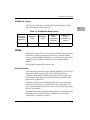
The PowerBase Embedded Controller Installation and Use manual provides
information you will need to install and use your PowerBase module, one of the
MVME130x family of PCI Mezzanine Card (PMC) carrier boards.
MVME1301
8MB DRAM, no parity
MVME1302
8MB DRAM, parity
MVME1305
16MB DRAM, no parity
MVME1306
16MB DRAM, parity
The manual includes hardware preparation and installation instructions,
information about using the front panel, a functional description, information
about programming the board, using the PPCBug debugging Þrmware, and
advanced debugger topics. Additional manuals you may wish to obtain are listed
in Appendix A, Ordering Related Documentation. Other appendices provide the
PowerBase speciÞcations, connector pin assignments, and a glossary of terms.
This manual is intended for anyone who wants to design OEM systems, supply
additional capability to an existing compatible system, or work in a lab
environment for experimental purposes. A basic knowledge of computers and
digital logic is assumed.
The PowerBase boards may be populated with a number of plug-together
components, including PMCs, PROM mezzanine, transition board, and Serial
Interface Modules (SIMs). Combinations of PowerBase boards and speciÞc
components are collectively referred to as PowerCom.
The information in this manual applies principally to the MVME130x PowerBase
boards. The PMCs, PROM mezzanine, transition modules, and SIMs are described
brießy here but are documented in detail in separate publications.
Document Terminology
Throughout this manual, a convention is used which precedes data and address
parameters by a character identifying the numeric format as follows:
$
0x
%
&
Dollar
Zero-x
Percent
Ampersand
Specifies a hexadecimal character
Specifies a binary number
Specifies a decimal number
For example, Ò12Ó is the decimal number twelve, and Ò$12Ó (hexadecimal) is the
equivalent of decimal number eighteen. Unless otherwise speciÞed, all address
references are in hexadecimal.
An asterisk (*) following the signal name for signals which are level-signiÞcant
denotes that the signal is true or valid when the signal is low.
An asterisk (*) following the signal name for signals which are edge-signiÞcant
denotes that the actions initiated by that signal occur on high-to-low transition.
In this manual, assertion and negation are used to specify forcing a signal to a
particular state. In particular, assertion and assert refer to a signal that is active or
true; negation and negate indicate a signal that is inactive or false. These terms are
used independently of the voltage level (high or low) that they represent.
Data and address sizes are deÞned as follows:
Byte
Half word
Word
Double word
8 bits, numbered 0 through 7,
with bit 0 being the least significant.
16 bits, numbered 0 through 15,
with bit 0 being the least significant.
32 bits, numbered 0 through 31,
with bit 0 being the least significant.
64 bits, numbered 0 through 63,
with bit 0 being the least significant.
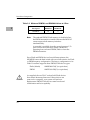
Safety Summary
Safety Depends On You
The following general safety precautions must be observed during all phases of operation, service, and
repair of this equipment. Failure to comply with these precautions or with speciÞc warnings elsewhere in
this manual violates safety standards of design, manufacture, and intended use of the equipment.
Motorola, Inc. assumes no liability for the customer's failure to comply with these requirements.
The safety precautions listed below represent warnings of certain dangers of which Motorola is aware. You,
as the user of the product, should follow these warnings and all other safety precautions necessary for the
safe operation of the equipment in your operating environment.
Ground the Instrument.
To minimize shock hazard, the equipment chassis and enclosure must be connected to an electrical ground.
The equipment is supplied with a three-conductor ac power cable. The power cable must be plugged into
an approved three-contact electrical outlet. The power jack and mating plug of the power cable meet
International Electrotechnical Commission (IEC) safety standards.
Do Not Operate in an Explosive Atmosphere.
Do not operate the equipment in the presence of ßammable gases or fumes. Operation of any electrical
equipment in such an environment constitutes a deÞnite safety hazard.
Keep Away From Live Circuits.
Operating personnel must not remove equipment covers. Only Factory Authorized Service Personnel or
other qualiÞed maintenance personnel may remove equipment covers for internal subassembly or
component replacement or any internal adjustment. Do not replace components with power cable
connected. Under certain conditions, dangerous voltages may exist even with the power cable removed. To
avoid injuries, always disconnect power and discharge circuits before touching them.
Do Not Service or Adjust Alone.
Do not attempt internal service or adjustment unless another person capable of rendering Þrst aid and
resuscitation is present.
Use Caution When Exposing or Handling the CRT.
Breakage of the Cathode-Ray Tube (CRT) causes a high-velocity scattering of glass fragments (implosion).
To prevent CRT implosion, avoid rough handling or jarring of the equipment. Handling of the CRT should
be done only by qualiÞed maintenance personnel using approved safety mask and gloves.
Do Not Substitute Parts or Modify Equipment.
Because of the danger of introducing additional hazards, do not install substitute parts or perform any
unauthorized modiÞcation of the equipment. Contact your local Motorola representative for service and
repair to ensure that safety features are maintained.
Dangerous Procedure Warnings.
Warnings, such as the example below, precede potentially dangerous procedures throughout this manual.
Instructions contained in the warnings must be followed. You should also employ all other safety
precautions which you deem necessary for the operation of the equipment in your operating environment.
!
WARNING
Dangerous voltages, capable of causing death, are present in
this equipment. Use extreme caution when handling, testing,
and adjusting.
This equipment generates, uses, and can radiate electro-magnetic energy. It
may cause or be susceptible to electro-magnetic interference (EMI) if not
WARNING installed and used in a cabinet with adequate EMI protection.
!
European Notice: Board products with the CE marking comply with the EMC Directive
(89/336/EEC). Compliance with this directive implies conformity to the following
European Norms:
EN55022 (CISPR 22)
Radio Frequency Interference
EN50082-1 (IEC801-2, IEC801-3, IEEC801-4)
Electromagnetic Immunity
The product also fulfills EN60950 (product safety) which is essentially the requirement for the Low
Voltage Directive (73/23/EEC).
This board product was tested in a representative system to show compliance with the above
mentioned requirements. A proper installation in a CE-marked system will maintain the required
EMC/safety performance.
All Motorola PWBs (printed wiring boards) are manufactured by UL-recognized
manufacturers, with a ßammability rating of 94V-0.
The computer programs stored in the Read Only Memory of this device contain
material copyrighted by Motorola Inc., 1995, and may be used only under a license
such as those contained in MotorolaÕs software licenses.
The software described herein and the documentation appearing herein are
furnished under a license agreement and may be used and/or disclosed only in
accordance with the terms of the agreement.
The software and documentation are copyrighted materials. Making unauthorized
copies is prohibited by law.
No part of the software or documentation may be reproduced, transmitted,
transcribed, stored in a retrieval system, or translated into any language or
computer language, in any form or by any means without the prior written
permission of Motorola, Inc.
Motorola¨ and the Motorola symbol are registered trademarks of Motorola, Inc.
PowerPC 603ª is a trademark of International Business Machines Corporation.
PowerPCª is a trademark of International Business Machines Corporation and is
used by Motorola with permission.
All other products mentioned in this document are trademarks or registered
trademarks of their respective holders.
© Copyright Motorola 1996
All Rights Reserved
Printed in the United States of America
May 1996
1Preparing and Installing
the PowerBase
1
Introduction
This manual provides general information, hardware preparation
and installation instructions, operating instructions, and a
functional description of the PowerBase general purpose VMEbus
board, based on the PowerPCª 603 microprocessor. PowerBase is
a powerful, low-cost embedded VME controller, as well as an
intelligent Peripheral Component Interconnect (PCI) Mezzanine
Card (PMC) carrier board. One of the primary applications for the
PowerBase board is as a Wide Area Network (WAN) Controller
module for the telecommunications market worldwide.
PowerBase Architecture
PowerBase consists of the base board, which may be an
MVME1301, MVME1302, MVME1305, or MVME1306. These
modules include support circuitry such as parity DRAM,
PROM/Flash memory, and bridges to the Industry Standard
Architecture (ISA) bus and the VMEbus.
PowerBaseÕs PMC carrier architecture allows flexible configuration
options and easy upgrades. It is designed to support one optional
add-on PROM mezzanine module plus two PMCs in a single
VMEmodule slot.
Optional PROM mezzanine board contains sockets for 4MB of OneTime-Programmable (OTP) PROM, organized as 64 bits wide.
Optional PMC products include capabilities such as Asynchronous
Transfer Mode (ATM), Fiber Distributed Data Interface (FDDI),
Fast Ethernet, Fast-Wide Small Computer System Interface (SCSI2), and high-speed serial connectivity.
The PowerBase board supports front panel and P2 I/O on PMC
slot 1, and front panel I/O only on PMC slot 2. Additionally, the 64
pins of I/O from PMC slot 1 are routed directly to P2. When
1-1
PowerBase Architecture
utilizing P2 I/O, it is necessary for customers to design their own
connectivity/transition scheme.
Note
Motorola offers a transition board, the MVME762, for use
with the PowerBase. However, this board was designed to
support only one configuration of a PowerBase/PMC
combination: the PowerCom (MVME130x with the
MPMC282-01x MC68360 PMC installed). For more details
on this transition board, refer to the MVME762 and
PowerCom documentation listed in Appendix A.
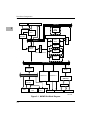
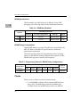
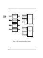
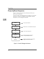
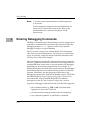
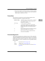
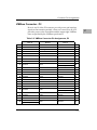
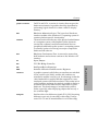
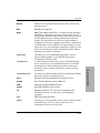
Figure 1-1 shows the PowerBase board and the positions of the
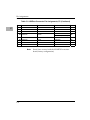
PMCs and PROM mezzanine. The block diagram in Figure 1-2
illustrates the architecture of the MVME130x base board.
Add-on PROM Module
LEDs
P1
Debug
Port
32MB ECC MEZ
Add-on PCI Mezzanine Card
PMC2
Front
Panel
I/O
(PMC2)
32MB ECC MEZ
PMC1
Front
Panel
or P2
I/O
Add-on PCI Mezzanine Card
P2
1
(PMC1)
PowerBase Board
11372
Figure 1-1. PowerBase with Optional PROM and PMC Mezzanines
1-2
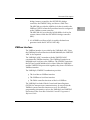
Preparing and Installing the PowerBase
Optional
MPC603
PROM/Flash
PROM
PowerPC
1 MB
4 MB
MPC603 Bus
MPC105
DRAM
8 or 16MB
Parity Option
PCI Bus
VME2PCI
ASIC
PCI/ISA Bridge
PMC Slot 1
PMC Slot 2
ISA Bus
VMEchip2
ASIC
PC16550
UART
VMEbus
Front Panel
or VMEbus P2
I/O
Front Panel
I/O
RJ45
Debug Port
VMEbus
P1 and P2
External I/O
11373
Figure 1-2. PowerBase Board Block Diagram
1-3
1
1
Equipment Required
PowerBase interfaces to the VMEbus via the P1 and P2 connectors.
It also draws +5V, +12V, and -12V power from the VMEbus
backplane through these two connectors. The +3.3V power, used
for the processor and PCI bridge chip and possibly for the PMC
mezzanine, is derived onboard from the +5V power.
Support for two IEEE P1386.1 PCI mezzanine cards is provided via
five 64-pin SMT connectors. Front panel openings are provided on
the PowerBase board for the two PMC slots. In addition, there are
64 pins of I/O from PMC slot 1 that are routed to P2. The two PMC
slots may contain two single width PMCs or one double width
PMC.
Equipment Required
The following equipment is required to utilize a PowerBase board:
❏
MVME130x base board (PowerBase)
❏
VMEsystem enclosure
The following equipment is optional:
❏
1-4
PROM mezzanine module
Preparing and Installing the PowerBase
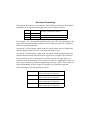
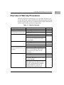
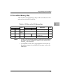
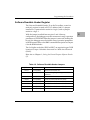
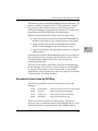
Overview of Start-Up Procedures
The following table lists the things you will need to do before you
can use this board, and tells where to find the information you need
to perform each step. Be sure to read this entire chapter and read all
Caution and Warning notes before beginning.
Table 1-1. Start-Up Overview
What you need to do ...
Unpack the hardware.
ConÞgure the hardware by
setting jumpers on the board.
Refer to ...
Unpacking the Hardware
ConÞguring the Hardware
Preparing the PowerBase
Install optional PMC(s), if any. Installing Optional PMCs
PMC Slots
For additional information on PMCs,
refer to the documentation furnished
with the PMCs.
Connect a console terminal.
Installing the Hardware
Debug Port
Installation Considerations
Connect any other optional
Connector Pin Assignments
devices or equipment you will For more information on optional
be using.
devices and equipment, refer to the
documentation provided with that
equipment.
Power up the system.
Installing the Hardware
Status Indicators (DS1 - DS4)
If any problems occur, refer to the section
Performing Diagnostic Tests in Chapter
5, Using PPCBug.
You may also wish to obtain the
PPC1Bug Diagnostics Manual, listed in
the table entitled Motorola Computer
Group Documents in Appendix A,
Ordering Related Documentation.
On page ...
1-7
1-7
1-8
1-17
2-4
1-13
2-3
1-18
C-1
1-13
2-2
5-17
1-5
1
1
Overview of Start-Up Procedures
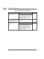
Table 1-1. Start-Up Overview (Continued)
What you need to do ...
Change any environmental
parameters as you wish.
Install the optional PROM
mezzanine, if desired (NOTE:
power must be off).
Program the MVME130x
module as needed for your
applications.
1-6
Refer to ...
ENV - Set Environment
You may also wish to obtain the PPCBug
Firmware Package UserÕs Manual, listed
in the table Motorola Computer Group
Documents in Appendix A, Ordering
Related Documentation.
Installing an Optional PROM
Mezzanine
On page ...
6-2
ConÞguring the Hardware
Programming the PowerBase
You may also wish to obtain the
PowerBase Embedded Controller
ProgrammerÕs Reference Guide, listed in
the table Motorola Computer Group
Documents in Appendix A, Ordering
Related Documentation.
1-7
4-1
1-15
Preparing and Installing the PowerBase
Unpacking the Hardware
Note
If the shipping carton is damaged upon receipt, request
that the carrier's agent be present during the unpacking
and inspection of the equipment.
Unpack the equipment from the shipping carton. Refer to the
packing list and verify that all items are present. Save the packing
material for storing and reshipping of equipment.
!
Avoid touching areas of integrated circuitry; static
discharge can damage these circuits.
Caution
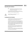
Configuring the Hardware
To produce the desired configuration and ensure proper operation
of the PowerBase board, you may need to carry out certain
modifications before and after installing the module.
The MVME130x provides software control over most options; by
setting bits in control registers after installing the MVME130x in a
system, you can modify its configuration. The MVME130x control
registers are described in Chapter 4, with additional information in
the PowerBase Embedded Controller Programmer's Reference Guide as
listed in table Motorola Computer Group Documents in Appendix
A, Ordering Related Documents.
Some options, however, are not software-programmable. Such
options are controlled through manual installation or removal of
header jumpers or interface modules on the base board or the
associated modules.
Serial ports on the optional PMC boards are manually configurable.
For a discussion of the configurable items on the PMCs, refer to the
userÕs manual for the particular PMC.
1-7
1
1
Preparing the PowerBase
Preparing the PowerBase
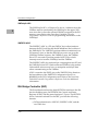
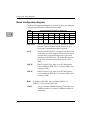
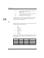
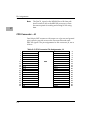
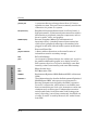
Figure 1-3 illustrates the placement of the switches, jumper
headers, connectors, and LED indicators on the MVME130x.
Manually configurable items on the base board include:
❏
General-purpose software-readable header (J2)
❏
VMEbus system controller selection (J5)
The MVME130x has been factory tested and is shipped with the
configurations described in the following sections. The MVME130x
factory-installed debug monitor, PPCBug, operates with those
factory settings.
Setting the General-Purpose Software-Readable Header (J2)
Header J2 provides eight readable jumpers. These jumpers can be
read as a register at ISA I/O address $801 (hexadecimal). Bit 0 is
associated with header pins 1 and 2; bit 7 is associated with pins 15
and 16. The bit values are read as a 0 when the jumper is installed,
and as a 1 when the jumper is removed. The MVME130x is shipped
from the factory with J2 set to all 0s (jumpers on all pins), as shown
in the diagram below.
J2
Bit 0 (SRH0)
1
PPCBug INSTALLED
2
Reserved for future use
Bit 1 (SRH1)
Setup parameter source (In=EEPROM; Out=ROM)
Bit 2 (SRH2)
Reserved for future use
Bit 3 (SRH3)
Board selection in WAN
Bit 4 (SRH4)
Board selection in WAN
Bit 5 (SRH5)
Board selection in WAN
Bit 6 (SRH6)
Board selection in WAN
Bit 7 (SRH7) 15
16
Board selection in WAN
The PowerPC firmware, PPCBug, reserves all bits, SRH0 to SRH7.
1-8
MVME
130X
J9
J4
A1
B1
C1
S1
J8
J3
PROM/FLASH
SOCKET
P1
PROM/FLASH
SOCKET
FAIL
PMC2
J1
DEBUG
PORT
XU2
CPU
PMC1
FAIL PMC2
LED LED
DS
DS
4
2
CPU PMC1
LED LED
DS
DS
1
3
XU1
RISC
WATCH
S2
DEBUG
PROM MEZ CONNECTOR
RESET
ABORT RESET
SWITCH SWITCH
ABORT
PROM MEZ CONNECTOR
CPU/DEBUG CONNECTOR
PMC2
VME BUS
P2
J14
PMC SLOT 1 I/O
A1
B1
C1
J12
PMC SLOT 1
A32
B32
C32
J22
J11
PMC SLOT 1
A32
B32
C32
SOFTWARE
READEABLE
HEADER
J5
15
3
2
1
16
1
11371.00 9602
J2
2
SYSTEM
CONTROLLER
HEADER
PMC SLOT 2
J21
PMC SLOT 2
PMC1
Figure 1-3. MVME130x Switches, LEDs, Headers, Connectors
1-9
1
Preparing and Installing the PowerBase
1
Preparing the PowerBase
With the jumper installed between pins 3 and 4 (factory
configuration), the debugger uses the current user setup/operation
parameters in EEPROM. When the jumper is removed (making the
bit a 1), the debugger uses the default setup/operation parameters
in ROM instead. Refer to the ENV command description in Chapter
6 for the ROM defaults.
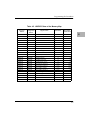
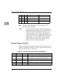
The five higher-order bits, SRH3 to SRH7, are required to get GCSR
locations for up to 18 boards when used in a Wide Area Network
(WAN). The MVME130x is shipped from the factory with J2 set to
all 0s (jumpers on all pins); each PowerBase board in the system
must have a unique address in order for the system to function
correctly. These addresses are given in Table 1-2.
There is a method to issue commands to the PPCBug on the
PowerBase board via the VMEbus. This method utilizes the Global
Control and Status Registers (GCSR) in the VMEchip2. Eight 16-bit
registers are included in the GCSR set. These registers are accessible
in the VMEbus short I/O space responding to address modifier
codes $29 or $2D. The specific address of the GCSR on the VMEbus
is programmed in the VMEchip2 LCSR by the debugger and is
determined by the conditions described below.
At start-up, PPCBug, when executing on PowerBase, reads the state
of the upper five jumpers on the software readable header J2. These
jumpers determine a board select number. Each board select
number has been assigned a specific group and board address in
VMEbus short I/O space, as shown in Table 1-2.
The specific assigned address is written into the LCSR and
EEPROM unless all five jumpers have been removed (board select
number 31). If all five jumpers are removed, then the values
previously stored in EEPROM for group and board addresses are
programmed in the LCSR. Values may be stored in the EEPROM by
setting the board select number with jumpers on J2, or with the
debugger ENV command. In this way, any jumper setting a board
select number other than 31 will over-ride and set the GCSR
address, yet any VMEbus short I/O address may be set using the
ENV command and the board select set to 31.
1-10
Preparing and Installing the PowerBase
Table 1-2. GCSR Addresses
Board
Select
Number
GCSR
Address
J2
Jumper
Setting
Notes
0
$FFFFD800
XXXIIIII
1, 2
1
$FFFFD810
XXX:IIII
1
2
$FFFFD820
XXXI:III
1
3
$FFFFD830
XXX::III
1
4
$FFFFD840
XXXII:II
1
5
$FFFFD850
XXX:I:II
1
6
$FFFFD860
XXXI::II
1
7
$FFFFD870
XXX:::II
1
8
$FFFFD880
XXXIII:I
1
9
$FFFFD890
XXX:II:I
1
10
$FFFFD8A0
XXXI:I:I
1
11
$FFFFD8B0
XXX::I:I
1
12
$FFFFD8C0
XXXII::I
1
13
$FFFFD8D0
XXX:I::I
1
14
$FFFFD8E0
XXXI:::I
1
Note: $FFFFD8F0 is not used.
15
$FFFFD900
XXX::::I
1
16
$FFFFD910
XXXIIII:
1
17
$FFFFD920
XXX:III:
1
18
$FFFFD930
XXXI:II:
1
Note: $FFFFD800 is used for all others
31
From EEPROM
XXX:::::
1
Notes 1. The first three jumper positions, for bits SRH0
through 2, may have unrelated functions. This is
represented above as XXX. An I = jumper installed on
the pins; a : = no jumper on the pins.
2. Default setting.
1-11
1
1
Preparing the PowerBase
Setting the VMEbus System Controller Selection Header (J5)
The MVME130x is factory-configured in automatic system
controller mode; i.e., a jumper is installed across pins 1 and 2 of
header J5. This means that the MVME130x determines if it is system
controller at system power-up or reset by its position on the bus; if
it is in slot 1 on the VME system, it configures itself as the system
controller.
Install the jumper across pins 2 and 3 if you intend to operate the
MVME130x as system controller in all cases.
Remove the jumper from J5 if the MVME130x is not to operate as
system controller under any circumstances.
J5
J5
1
1
1
2
2
2
3
3
3
Automatic System Controller
(factory configuration)
1-12
J5
System Controller Enabled
System Controller Disabled
Preparing and Installing the PowerBase
Installing the Hardware
The following paragraphs discuss the installation of the PowerBase
into a VME chassis, and installing the optional PMC boards and
PROM mezzanine board onto the PowerBase.
Taking ESD Precautions
Use ESD
Wrist Strap
Motorola strongly recommends that you use an antistatic wrist
strap and a conductive foam pad when installing or upgrading a
system. Electronic components, such as disk drives, computer
boards, and memory modules, can be extremely sensitive to
Electro-Static Discharge (ESD). After removing the component
from the system or its protective wrapper, place the component flat
on a grounded, static-free surface (and in the case of a board,
component side up). Do not slide the component over any surface.
If an ESD station is not available, you can avoid damage resulting
from ESD by wearing an antistatic wrist strap (available at
electronics stores) that is attached to an unpainted metal part of the
system chassis.
Installing the PowerBase
Before installing the PowerBase into your VME chassis, ensure that
the jumpers on PowerBaseÕs J2 and J5 headers are configured, as
previously described. If you intend to mount the optional PCI
mezzanine cards (PMCs) or PROM mezzanine on your PowerBase,
refer to the sections Installing Optional PMCs and Installing the
Optional PROM Mezzanine before you begin this procedure.
Proceed as follows to install the PowerBase in the VME chassis:
1. Attach an ESD strap to your wrist. Attach the other end of the
ESD strap to the chassis as a ground. The ESD strap must be
secured to your wrist and to ground throughout the
procedure.
2. Perform an operating system shutdown:
a. Turn the AC or DC power off and remove the AC cord or
DC power lines from the system.
1-13
1
1
Installing the Hardware
!
Inserting or removing modules with power applied
may result in damage to module components.
Caution
!
Warning
Dangerous voltages, capable of causing death, are
present in this equipment. Use extreme caution when
handling, testing, and adjusting.
b. Remove chassis or system cover(s) as necessary for access
to the VMEmodules.
3. Remove the filler panel from the card slot where you are
going to install the PowerBase board.
Ð If you intend to use the MVME130x as system controller, it
must occupy the leftmost card slot (slot 1). The system
controller must be in slot 1 to correctly initiate the busgrant daisy-chain and to ensure proper operation of the
IACK daisy-chain driver.
Ð If you do not intend to use the MVME130x as system
controller, it can occupy any unused card slot.
!
Avoid touching areas of integrated circuitry; static
discharge can damage these circuits.
Caution
4. Slide the MVME130x into the selected card slot. Be sure the
module is seated properly in the P1 and P2 connectors on the
backplane. Do not damage or bend connector pins.
5. Secure the MVME130x in the chassis with the screws
provided, making good contact with the transverse mounting
rails to minimize RF emissions.
Note
1-14
Some VME backplanes (e.g., those used in Motorola
ÒModular ChassisÓ systems) have an auto-jumpering
feature for automatic propagation of the IACK and BG
signals. Step 6 does not apply to such backplane
designs.
Preparing and Installing the PowerBase
6. On the chassis backplane, remove the INTERRUPT
ACKNOWLEDGE (IACK) and BUS GRANT (BG) jumpers from
the header for the card slot occupied by the MVME130x.
7. If you intend to use PPCBug interactively, connect the
terminal that is to be used as the PPCBug system console to
the DEBUG port on the front panel of the PowerBase. Set up
the terminal as follows:
Ð Eight bits per character
Ð One stop bit per character
Ð Parity disabled (no parity)
Ð Baud rate = 9600 baud (default baud rate of the port at
power-up)
In normal operation the host CPU controls PowerBase
operation via the VMEbus GCSR registers (refer to
MultiProcessor Support in Chapter 5). In normal operation,
connection of a debug console terminal is required only if you
intend to use PPCBug interactively.
8. Replace the chassis or system cover(s), cable peripherals to
the panel connectors as appropriate, reconnect the system to
the AC or DC power source, and turn the equipment power
on.
9. The MVME130xÕs CPU LED indicates activity as a set of
confidence tests is run, and the debugger prompt PPC1-Bug>
appears.
Installing the Optional PROM Mezzanine
!
Caution
When you install the PROM Mezzanine on your PowerBase, the
Flash devices will be inaccessible, and you will not be able to use the
PPCBug functions in Flash.
Proceed as follows to install the optional PROM mezzanine on your
PowerBase board:
1-15
1
1
Installing the Hardware
1. Attach an ESD strap to your wrist. Attach the other end of the
ESD strap to the chassis as a ground. The ESD strap must be
secured to your wrist and to ground throughout the
procedure.
Note
If your MVME130x has not yet been installed in a
chassis, go to step 4.
2. Perform an operating system shutdown:
a. Turn the AC or DC power off and remove the AC cord or
DC power lines from the system.
!
Inserting or removing modules with power applied
may result in damage to module components.
Caution
!
Warning
Dangerous voltages, capable of causing death, are
present in this equipment. Use extreme caution when
handling, testing, and adjusting.
b. Remove chassis or system cover(s) as necessary for access
to the VMEmodules.
3. Remove the screws securing the MVME130x to the chassis
and remove the MVME130x from its card slot.
4. Lay the MVME130x on a level surface with the P1 and P2
connectors on your right, and position the PROM mezzanine
above it in the upper right-hand corner. (Refer to Figure 1-1.)
!
Caution
1-16
Avoid touching areas of integrated circuitry; static
discharge can damage these circuits.
Preparing and Installing the PowerBase
5. Gently seat the PROM mezzanine onto the PowerBase
module, ensuring that the connectors are properly aligned.
(Refer to Figure 1-3.)
6. Using the provided screws, fasten the PROM mezzanine to
the MVME130x.
7. Reinstall the MVME130x board in the chassis according to the
instructions given in the Installing the PowerBase section of this
chapter.
Installing Optional PMCs
Proceed as follows to install optional PCI mezzanine cards (PMCs)
on your PowerBase board:
1. Attach an ESD strap to your wrist. Attach the other end of the
ESD strap to the chassis as a ground. The ESD strap must be
secured to your wrist and to ground throughout the
procedure.
Note
If your MVME130x has not yet been installed in a
chassis, go to step 4.
2. Perform an operating system shutdown:
a. Turn the AC or DC power off and remove the AC cord or
DC power lines from the system.
!
Inserting or removing modules with power applied
may result in damage to module components.
Caution
!
Warning
Dangerous voltages, capable of causing death, are
present in this equipment. Use extreme caution when
handling, testing, and adjusting.
1-17
1
1
Installation Considerations
b. Remove chassis or system cover(s) as necessary for access
to the VMEmodules.
3. Remove the screws securing the MVME130x to the chassis
and remove the MVME130x from its card slot.
4. Lay the MVME130x on a level surface with the P1 and P2
connectors closest to you, and position the PMC above it in
the center (for PMC2) or left-hand side (for PMC1). (Refer to
Figure 1-1.)
!
Avoid touching areas of integrated circuitry; static
discharge can damage these circuits.
Caution
5. Insert the PMCÕs front panel bezel through the selected PMC
slot in the PowerBaseÕs front panel and gently seat the PMC
onto the PowerBase, ensuring that the keying pin and
connectors are properly aligned. (Refer to Figure 1-3.)
6. Turn the PowerBase over, and using the four provided
screws, fasten the PMC to the MVME130x from the
underside.
7. Reinstall the MVME130x board in the chassis according to the
instructions given in the Installing the PowerBase section of this
chapter.
Installation Considerations
The PowerBase board draws power from the VMEbus backplane
connectors P1 and P2. P2 is also used for the upper 16 bits of data in
32-bit transfers, and for the upper 8 address lines in extended
addressing mode. The MVME130x may not function properly
without its main board connected to VMEbus backplane connectors
P1 and P2.
Whether the PowerBase operates as a VMEbus master or as a
VMEbus slave, it is configured for 32 bits of address and 32 bits of
data (A32/D32). However, it handles A16 or A24 devices in the
1-18
Preparing and Installing the PowerBase
address ranges indicated in Chapter 4. D8 and/or D16 devices in
the system must be handled by the PowerPC processor software.
Refer to the memory maps in Chapter 4.
The MVME130x contains shared onboard DRAM whose base
address is software-selectable. Both the onboard processor and offboard VMEbus devices see this local DRAM at base physical
address $00000000, as programmed by the PPCBug firmware. This
may be changed via software to any other base address. Refer to the
PowerBase Programmer's Reference Guide for more information.
If the MVME130x tries to access off-board resources in a
nonexistent location and is not system controller, and if the system
does not have a global bus time-out, the MVME130x waits forever
for the VMEbus cycle to complete. This will cause the system to lock
up. There is only one situation in which the system might lack this
global bus time-out: when the MVME130x is not the system
controller and there is no global bus time-out elsewhere in the
system.
Multiple PowerBase boards may be installed in a single VME
chassis. Each must have a unique GCSR address, selected by setting
jumpers on its J2 header, as described in Preparing the PowerBase. In
general, hardware multiprocessor features are supported.
Other MPUs on the VMEbus can interrupt, disable, communicate
with, and determine the operational status of the processor(s). One
register of the GCSR (global control/status register) set includes
four bits that function as location monitors to allow one MVME130x
processor to broadcast a signal to any other MVME130x processors.
All eight registers are accessible from any local processor as well as
from the VMEbus.
1-19
1
1
Installation Considerations
1-20
2Using the Front Panel
2
Introduction
This chapter provides information about the switches, status
indicators, and I/O ports on the front panel of the PowerBase. The
front panel is pictured in Figure 1-3 in Chapter 1.
Switches
There are two switches (ABORT and RESET) and four LED (lightemitting diode) status indicators (CPU, FAIL, PMC1, PMC2) located on
the MVME130x front panel.
ABORT (S1)
When activated by software, the ABORT switch can generate an
interrupt signal from the base board to the processor at a userprogrammable level. The interrupt is normally used to abort
program execution and return control to the PPCBug debugger
firmware located in the PowerBase Flash or PROM memory. The
interrupt signal reaches the processor module via ISA bus interrupt
line IRQ8*. The signal status is also available from the general
purpose I/O port (refer to Chapter 4). This also allows software,
after an IRQ8* interrupt, to poll the ABORT switch and verify that it
has been pressed.
The interrupter connected to the ABORT switch is an edge-sensitive
circuit, filtered to remove switch bounce.
RESET (S2)
The RESET switch resets all onboard devices and causes HRESET*
to be asserted in the MPC603; it also drives a SYSRESET* signal if
the PowerBase is the system controller.
The VMEchip2 includes both a global and a local reset driver. When
the VMEchip2 operates as the VMEbus system controller, the reset
2-1
Status Indicators (DS1 - DS4)
driver provides a global system reset by asserting the VMEbus
signal SYSRESET*. A SYSRESET* signal may be generated by the
RESET switch, a power-up reset, a watchdog time-out, or by a
control bit in the LCSR in the VMEchip2. SYSRESET* remains
asserted for at least 200 ms, as required by the VMEbus
specification.
2
Similarly, the VMEchip2 provides an input signal and a control bit
to initiate a local reset operation. By setting a control bit, software
can maintain a board in a reset state, disabling a faulty board from
participating in normal system operation. The local reset driver is
enabled even when the VMEchip2 is not the system controller. A
local reset may be generated by the RESET switch, a power-up reset,
a watchdog time-out, a VMEbus SYSRESET*, or a control bit in the
GCSR.
Status Indicators (DS1 - DS4)
There are four LED (light-emitting diode) status indicators located
on the MVME130x front panel.: CPU, FAIL, PMC1, and PMC2.
CPU (DS1)
This green LED indicates CPU activity; lights when the DBB* (Data
Bus Busy) signal line on the processor bus is active.
FAIL (DS4)
This yellow LED indicates board failure; lights when the BRDFAIL*
signal line is active.
PMC1 (DS3)
This green LED indicates PCI activity; lights when the PCI bus grant
to PMC1 signal line on the PCI bus is active. This indicates that a
PMC (if installed) is active.
PMC2 (DS2)
This green LED indicates PCI activity; lights when the PCI bus grant
to PMC2 signal line on the PCI bus is active. This indicates that a
PMC (if installed) is active.
2-2
Using the Front Panel
DEBUG Port
2
The RJ45 port labeled DEBUG on the front panel of the PowerBase
supplies the PowerBase serial communications interface,
implemented via a UART PC16550 controller chip from National
Semiconductor. It is asynchronous only. This serial port is
configured for EIA-232-D DTE, as shown in Figure 2-1.
The DEBUG port may be used for connecting a terminal to the
PowerBase to serve as the firmware console for PowerBaseÕs factory
installed debugger, PPCBug. The port is configured as follows:
❏
8 bits per character
❏
1 stop bit per character
❏
Parity disabled (no parity)
❏
Baud rate = 9600 baud (default baud rate at power-up)
SOUT
4
RTS*
2
DTR*
8
SIN
5
CTS*
7
DCD*
1
3
6
PC16550
PowerBase
Debug
RJ45
Figure 2-1. Debug Port Configuration
2-3
PMC Slots
After power-up, the baud rate of the DEBUG port can be
reconfigured by using the debuggerÕs Port Format (PF) command.
Refer to Chapters 5 and 6 for information about PPCBug.
2
PMC Slots
Two openings located on the front panel provide I/O expansion by
allowing access to one or two single-wide or one double-wide PCI
Mezzanine Card (PMC), connected to the PMC connectors on the
PowerBase. For pin assignments for the PMC connectors, refer to
Appendix C.
!
Warning
Do not attempt to install any PMC boards without
performing an operating system shutdown and
following the procedures given in Chapter 1.
For further information on PMCs, refer to the userÕs manual for the
particular PMC.
PMC1 (PMC Slot 1)
The opening labeled PMC1 on the front panel provides I/O access to
a PMC when it is connected to the 64-pin SMT connectors J11 and
J12 on the PowerBase board.
When a PMC is connected to the 64-pin SMT connectors J11, J12,
and J14 on the PowerBase board, 64 pins of I/O from PMC slot 1 are
routed to P2, the 96-pin VMEbus connector on the back of the
PowerBase board. Both P2 and the front panel are then accessible
for I/O.
PMC2 (PMC Slot 2)
The opening labeled PMC2 on the PowerBase front panel provides
I/O access to a PMC when it is connected to 64-pin SMT connectors
J21 and J22 on the PowerBase board.
Double-Wide PMCs
A double-wide, 8-port PMC, connected to J11, J12, J21, and J22,
would allow front panel I/O access through both PMC1 and PMC2,
and optionally the P2 connector if J14 is also used.
2-4
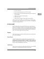
3Functional Description
3
Introduction
This chapter describes the PowerBase embedded controller on a
block diagram level. The General Description provides an overview
of the MVME130x, followed by a detailed description of several
blocks of circuitry. Figure 3-1 shows a block diagram of the overall
board architecture.
Detailed descriptions of other MVME130x blocks, including
programmable registers in the ASICs and peripheral chips, can be
found in the PowerBase Embedded Controller ProgrammerÕs Reference
Guide. Refer to it for a functional description of the MVME130x in
greater depth.
General Description
The PowerBase is a general purpose, high-performance, embedded
controller VMEmodule based on the 66MHz PowerPC 603
microprocessor.
As shown in the PowerBase Features section, PowerBase offers many
standard features desirable in a computer system, including a
debug port, Boot ROM, PROM/Flash memory, DRAM, and
interface for two PCI Mezzanine Cards (PMCs), contained in a oneslot VME package. Its flexible mezzanine architecture allows
relatively easy upgrades of the I/O and/or memory.
There are four standard buses on PowerBase:
PowerPC 603 Processor Bus
PCI Local Bus
ISA Bus
VMEbus
3-1
PowerBase Features
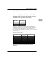
As shown in Figure 3-1, an MPC105 PCI Bridge/Memory
Controller provides the interface from the Processor Bus to PCI. An
82378ZB device performs the bridge function between PCI and ISA.
Two ASIC devices, VME2PCI and VMEchip2, provide the interface
between the PCI Local Bus and the VMEbus.
3
The PCI local bus is a key feature. In addition to the on-board local
bus peripherals, the PCI bus supports an industry-standard
mezzanine interface, IEEE P1386.1 PMC (PCI Mezzanine Card).
PowerBase Features
The base board contains the following:
❏
66.66MHz MPC603 PowerPCTM processor
❏
8 or 16MB of DRAM, with or without parity (build options)
❏
1MB of onboard PROM/Flash memory for Boot ROM
❏
Option for 4MB of PROM on a mezzanine board
❏
VMEbus interface implemented with VMEchip2 ASIC
Ð VMEbus system controller functions
Ð VMEbus interface to local bus (A24/A32,
D8/D16/D32/BLT(D8/D16/D32/D64))
Ð Local bus to VMEbus interface (A16/A24/A32,
D8/D16/D32)
Ð VMEbus interrupter
Ð VMEbus interrupt handler
Ð Global CSR for interprocessor communications
Ð DMA for fast local memory - VMEbus transfers
(A16/A24/A32, D16/D32/D64).
❏
Interfaces to two P1386.1 PCI Mezzanine Cards (PMCs)
Ð Accepts two single-width PMCs or one double-width
PMC
Ð Front panel and/or VMEbus P2 I/O on PMC slot 1
3-2
Functional Description
Ð Front panel I/O on PMC slot 2
❏
One asynchronous serial port (debug port) via an RJ45 front
panel connector
❏
8-bit Software Readable Header
❏
8KB of EEPROM
❏ RESET
switch
❏ ABORT
switch
❏
Status LEDs for FAIL, CPU, PMC1, and PMC2
Refer to Appendix B for product specifications.
PowerBase Components
Figure 3-1 is a block diagram of the MVME130xÕs overall
architecture.
RISCWatch Header
A 16-pin male 2x8 header is provided for connecting to the
RISCWatch MPC603 processor interface. MPC603 interconnect
information is provided in Appendix C.
PCI Bridge/Memory Controller (MPC105)
A Motorola MPC105 device provides the necessary interface
between the MPC603 processor, the Flash memory, the PROM, the
DRAM, and the PCI Local Bus. The MPC105 supports various
PowerPC processor external bus frequencies up to 66.66MHz and
PCI frequencies up to 33.33MHz. Table 3-1 summarizes the clock
frequencies supported by the PowerBase:
3-3
3
PowerBase Components
CPU Connector
MPU Bus
Optional
4MB
PROM
3
MPC603
MPU
Clock
Generator
PROM Mezzanine Connector
Buffers
MPU Bus
MPC105
Bridge
PROM/
Flash
1Mx8
Buffers
RISCwatch
DRAM
8MB
Data
DRAM
8MB
Optional
Address and Control
DRAM
Parity
Optional
PCI Local Bus
82378ZB
ISA Bridge
ISA Bus
VME2PCI
Bridge
PMC Slot 2
PMC Slot 1
VME
VMEchip2
Decode
Function
Buffers
CSRs
EEPROM
8Kx8
PC16550
UART
Front Panel
P2 Connector
P1 Connector
11414.00
Figure 3-1. MVME130x Block Diagram
3-4
Functional Description
Table 3-1. MPC603 Clock Frequencies Supported by PowerBase
MPC603
Internal
Processor
Speed
MPC603
MPC603
External
Clock PLL
Bus Speed
MPC105
MPC105
Internal
External
MPC105
PCI Bus
Clock
Clock
Clock PLL Frequency
Frequency Frequency
66.66MHz
66.66MHz
66.66MHz
1x
33.33MHz
2x
33.33MHz
Flash Devices and Boot ROM
The PowerBase has two onboard 32-pin PLCC sockets which
support two banks of 512Kx8 PROM or Flash devices that together
provide a total of 1MB of PROM/Flash capacity. This memory
space is provided for the Boot ROM function.
The factory configuration is with Flash devices installed. Since the
devices are socketed, they are programmed externally before they
are installed on the board. The onboard monitor/debugger,
PPCBug, resides in the Flash devices. PPCBug provides:
❏
A boot loader and extensive on-board diagnostics
❏
A single-line assembler-disassembler
❏
A remote boot capability
Each bank of PROM/Flash is 8-bits wide and is controlled by the
MPC105. The MPC105 performs byte alignment for write accesses
and also packs bytes for 16-bit, 32-bit, and 64-bit read accesses to the
PROM/Flash area.
The PROM/Flash must be accessed in the MPC105 non-burst
mode. For PROM/Flash speed of 150ns, software should program
ROMFAL (first access length) and ROMNAL (last access length) in
the MPC105 device with the following values:
3-5
3
PowerBase Components
Table 3-2. Minimum ROMFAL and ROMNAL Values at 150ns
3
Processor External
Bus Speed
Minimum
ROMFAL
Minimum
ROMNAL
66.66MHz
10
0
Note
The onboard PROM/Flash memory is disabled when
the PROM mezzanine is installed, because the MPC105
cannot support both memory interfaces
simultaneously.
A status bit is available from the general purpose I/O
port to allow the firmware to know whether it is
operating from on-board PROM/Flash or from the
PROM mezzanine.
Since Flash and PROM devices have different pinouts, the
MVME130x must be hard-wired with zero-ohm resistors for Flash
or PROM memory configuration. The factory configuration is for
Flash. PowerBase supports these PROM/Flash device types:
!
Caution
3-6
Flash (default)
AM29F040-150JC (or equivalent)
PROM
AM27C040-150JC (or equivalent)
As supplied, the two PLCC sockets hold Flash devices
that contain bootstrap firmware. If these devices are
removed or corrupted, your system will not boot.
Replacement PROM/Flash devices must have board
initialization and boot capability.
Functional Description
PROM/Flash Latency
The following table shows the PROM/Flash read latency at the
processor/memory bus frequency:
3
Table 3-3. PROM/Flash Read Latency
Processor
External Bus
Frequency
ROMFAL
Value
ROMNAL
Value
8-Bit Access
Times
(in number
of clocks)
64-Bit Access
Times
(in number of
clocks)
66.66MHz
10
0
14
98
DRAM
The MPC105 supports one or two banks of DRAM. The PowerBase
base board contains one bank (four devices) of 1Mx16 DRAM
devices providing 8MB of DRAM, or as a build option, two banks
(eight devices) of 1Mx16 DRAM devices providing 16MB of
DRAM.
The DRAM is organized as 64-bits wide.
Parity Protection
Optional parity protection is provided by eight 4Mx1 TSOP devices
mounted on the back side of the board. The board may be
configured with 8MB or 16MB of non-parity memory with only
front-side mounted chips, but for parity memory, the back side
must also be populated.
Since the parity devices are 4M deep and the two main memory
banks are only 1M deep, one 4Mx1 device provides parity for a
given byte of both memory banks. Thus, only a total of eight parity
devices are required.
A status bit available from the general purpose I/O port allows the
firmware to know whether parity is present or not. This bit is
controlled by a pulldown resistor.
3-7
PowerBase Components
DRAM Specifications
The PowerBase uses 1Mx16 devices in 400 mil, 50 pin TSOP
packaging. The following table lists the DRAM specifications:
3
Table 3-4. DRAM Specifications
DRAM SpeciÞcations
Options
Quantity
Size and ConÞguration
Package
Speed
8MB
Main
4
1M x 16
400 mil TSOP
60ns
16MB
Main
8
1M x 16
400 mil TSOP
60ns
DRAM Timing Configurations
Onboard DRAM devices on the PowerBase are controlled by the
MPC105. Refer to the MPC105 specification for additional
performance information.
The following table shows the programming values including
latency for the MPC105 timing configurations required for 60ns
DRAM at the processor/memory bus frequency:
Table 3-5. Programming Values for DRAM Timing Configurations
Processor
External Bus
Frequency
Read/Write Timing ConÞgurations
RP1
RCD2
CAS3
CP4
CAS5
RAS6P
DRAM
Latency
66.66MHz
3
2
4
1
3
4
8-4-4-4
Clocks
There are two oscillators on the PowerBase board:
1. A 14.31818MHz oscillator which feeds an MPC980 clock
driver chip. The MPC980 provides the 66.6MHz and
33.3MHz clocks for the MPC603 processor, the MPC105
3-8
Functional Description
bridge/memory controller, the 82378ZB ISA bridge
controller, the VME2PCI chip, and the two PMC slots.
The MPC980 provides the 16MHz clock that is used for the
VMEbus SYSCLK when the PowerBase board is configured
as the VMEbus system controller.
The MPC980 also provides the 14.31818MHz clock for the
counter/timers inside the 82378ZB ISA bridge controller
(IBC). .
2. A 1.8432MHz oscillator which is used by the baud rate
generator inside the PC16550 UART chip.
VMEbus Interface
The VMEbus interface is provided by the VMEchip2 ASIC. Since
the VMEchip2 local bus interface is the MC68040 bus, the VME2PCI
ASIC is also required.
The VMEchip2 ASIC, in tandem with the VME2PCI ASIC,
constitutes the VMEbus interface. The VMEchip2 interfaces an
MC68040-style local bus to the VMEbus. The VME2PCI interfaces
the PCI bus to an MC68040-style local bus. When the VMEchip2
and the VME2PCI chips are used together, they form a PCI-bus-toVMEbus interface.
The VMEchip2/VME2PCI combination provides:
❏
The local-bus-to-VMEbus interface
❏
The VMEbus-to-local-bus interface
❏
The DMA controller functions of the local VMEbus
The VMEchip2 includes Global Control and Status Registers
(GCSRs) for interprocessor communications. It can provide the
VMEbus system controller functions as well. For detailed
programming information, refer to the VMEchip2 and VME2PCI
discussions in the PowerBase Embedded Controller Programmer's
Reference Guide.
3-9
3
PowerBase Components
VMEchip2 ASIC
The VMEchip2 ASIC is a 324-pin LGA device. Addresses from the
VMEbus must be translated by the VMEchip2 to the upper 2GB
area since that is where the onboard DRAM is mapped in the PCI
memory space. Refer to the PowerBase Embedded Controller
ProgrammerÕs Reference Guide for programming information on the
VMEchip2.
3
VME2PCI ASIC
The VME2PCI ASIC is a 225-pin OMPAC device that interfaces
between the PCI Local Bus and the MC68040 bus (the local bus of
the VMEchip2). The VME2PCI performs address translation from
PCI memory space so that the MPC603 processor can get to the
VMEchip2 internal registers, the VMEbus F-page, the VMEbus
Short I/O area, and to perform pseudo IACK cycles to fetch
interrupt vectors from the VMEchip2 and the VMEbus.
The VME2PCI ASIC also performs byte swapping between PCI and
the VMEchip2 since PCI is little-endian and VMEbus is big-endian.
Little-endian software may have to manipulate multi-byte data
when communicating to the VMEbus.
AD13 is routed to the IDSEL pin on the VME2PCI chip; therefore
the base address of the VME2PCI Configuration Space is at
$00802000 in the PCI Configuration area. Refer to the PowerBase
Embedded Controller ProgrammerÕs Reference Guide for additional
information.
ISA Bridge Controller (IBC)
The PowerBase board uses the Intel 82378ZB to interface to the ISA
bus for the debug port, the EEPROM, the Control and Status
Registers (CSRs), and the general purpose I/O port. The 82378ZB
device, hereafter referred to as the IBC, provides the following
features:
❏
3-10
PCI bus arbitration for: MPC105, VME2PCI ASIC, and the
two PMC slots
Functional Description
❏
ISA bus arbitration
❏
ISA interrupt mapping for four PCI interrupts
❏
Functionality of two 82C59 interrupt controllers to support 14
ISA interrupts
❏
Edge/level control for ISA interrupts
❏
One 16-bit timer
❏
Three interval counters/timers (82C54 functionality)
AD11 is routed to the IDSEL pin on the IBC device; therefore the
base address of the configuration space for the IBC is at $00800800
in the PCI configuration area.
PC16550 UART
The PowerBase board uses a PC16550 Universal Asynchronous
Receiver/Transmitter (UART) to provide the asynchronous debug
port. TTL-level signals for the port are routed through appropriate
EIA-232-D drivers and receivers to an RJ45 connector on the front
panel. The external signals are ESD protected.
Timers
Timers and counters on the PowerBase board are provided by the
IBC and the VMEchip2.
Interval Timers
The IBC has three built-in counters that are equivalent to those
found in an 82C54 programmable interval timer. These counters are
grouped into one timer unit, Timer 1, in the IBC. These counters use
the OSC clock input as their clock source. The PowerBase drives the
OSC pin with a 14.31818MHz clock source.
16-Bit Timers
There is one 16-bit timer provided by the IBC. Refer to the 82378ZB
data sheet for programming information on this timer.
3-11
3
PowerBase Components
VMEchip2 Timers
There are two programmable 32-bit timers in the VMEchip2. Refer
to the PowerBase Embedded Controller ProgrammerÕs Reference Guide
for programming information on the VMEchip2.
3
EEPROM
There is one 28C64 EEPROM device that provides 8KB of nonvolatile storage for configuration information and environment
variables. Refer to Chapter 6 for more about the configurable
environment parameters.
PROM Mezzanine Card Slot
The PowerBase provides for an add-on PROM mezzanine board.
The PROM mezzanine interface to the PowerBase is via two 64-pin
connectors. These connectors are the same type as those used for
PMC boards. The PROM mezzanine provides eight 32-pin PLCC
sockets that support one bank of 512Kx8 devices for a total of 4MB
of PROM memory. The memory is organized as 64 bits wide and is
controlled by the MPC105.
When installed, the PROM mezzanine will disable the onboard
PROM/Flash memory because the MPC105 cannot support both
memory interfaces simultaneously. The supported package is for
one-time programmable (OTP) PLCC devices. The appropriate
PROM device type is AM27C040-150JC (or equivalent). Since the
devices are socketed, it is assumed that they must be programmed
externally before installation on the board.
Note
3-12
The PROM mezzanine can optionally be configured to use
PLCC Flash devices by changing several zero-ohm
resistors on the PROM mezzanine board. The Flash devices
in such a configuration will not be reprogrammable incircuit, however. They must be reprogrammed with an
external programmer. The appropriate Flash device type is
AM29F040-150JC (or equivalent).
Functional Description
The PROM must be accessed in the MPC105 non-burst mode. For
PROM speed of 150ns, software should program ROMFAL and
ROMNAL in the MPC105 device with the following values:
3
Table 3-6. Minimum ROMFAL and ROMNAL Values at 150ns
Processor External
Bus Speed
66.66MHz
Minimum
ROMFAL
10
Minimum
ROMNAL
0
A status bit is available from the general purpose I/O port to allow
the firmware to know whether it is operating from on-board
PROM/Flash or from the PROM mezzanine.
PCI Mezzanine Card (PMC) Slots
The PowerBase board supports two PMC slots. Five 64-pin
connectors are located on the PowerBase board to interface to two
32-bit IEEE P1386.1 PMCs to add any desirable function. The PMC
slots have the characteristics listed below. For detailed
programming information, refer to the programmerÕs reference
guide and to the user documentation for the PMC modules you
intend to use.
PMC1
PMC slot 1 supports:
Mezzanine type:
PCI Mezzanine Card (PMC)
Mezzanine size:
Single width and standard depth (75mm x
150mm) with front panel
PMC connectors:
J11, J12, and J14 (32-Bit PCI with frontpanel or P2 I/O)
Signalling voltage:
Vio = 5.0V
AD16 is routed to the IDSEL pin on PMC slot 1; therefore the base
address of the configuration space of this PMC slot is at $00810000
in the PCI configuration area.
3-13
PowerBase Components
PMC2
PMC slot 2 supports:
3
Mezzanine type:
PCI Mezzanine Card (PMC)
Mezzanine size:
Single width and standard depth (75mm x
150mm) with front panel
PMC connectors:
J21 and J22 (32-Bit PCI with front-panel
I/O only)
Signalling voltage:
Vio = 5.0V
AD17 is routed to the IDSEL pin on PMC slot 2; therefore the base
address of the configuration space of this PMC slot is at $00820000
in the PCI configuration area.
Double-Width PMC
The PMC connectors are located such that a double width PMC
may be installed in place of the two single width PMCs.
In this case, the PowerBase supports the following:
Mezzanine type:
PCI Mezzanine Card (PMC)
Mezzanine size:
Double width and standard depth (150mm
x 150mm) with front panel
PMC connectors:
J11, J12, J21, J22, and J14 (32-bit PCI with
front-panel or P2 I/O)
Signalling voltage:
Vio = 5.0V
For the double width PMC, it may pick up AD16 from the PMC slot
1 connector or AD17 from the PMC slot 2 connector; therefore the
base address of the configuration space of this PMC may be at
$00810000 or $00820000 in the PCI Configuration area.
Transition Board Power
The PowerBase board supplies +12V, -12V, +5V and +3.3V to the
PMCs. Because PMC1 is wired directly to the 64 I/O pins of P2, it
must provide power to any transition board with which it
3-14
Functional Description
communicates. On the PowerBase board, the four pins that are used
to provide power to the MVME762 transition module have
polyswitches in series for overcurrent protection (factory
configuration). A build option, for use with other transition boards,
can provide direct connections with no polyswitches.
Note
If the pins are used for high-speed signals, you should
evaluate the signal integrity.
If power fault protection is desired for transition boards other than
the MVME762, it must be provided by the corresponding PMC
module since it directly provides power to the transition module.
For the purposes of calculating how many power pins are required
for a transition board, the following trace widths are present on
PowerBase for the PMC1 I/O pins:
Header
J14
Pin
10
17
28
37
46
55
64
All others
Trace Width
50 mil
75 mil
50 mil
20 mil
20 mil
60 mil
50 mil
10 mil
3-15
3
PowerBase Components
3
3-16
4Programming the PowerBase
4
Introduction
This chapter provides basic information useful in programming
your PowerBase. This includes a description of memory maps,
control and status registers, PCI arbitration, interrupt handling,
sources of reset, and big/little endian issues.
For complete programming information, refer to the PowerBase
Embedded Controller ProgrammerÕs Reference Guide.
Memory Maps
There are multiple buses on the PowerBase and each bus domain
has its own view of the memory map. The following sections
describe the PowerBase memory organization from the following
three points of view:
❏
The mapping of all resources as viewed by the processor
(MPU bus memory map)
❏
The mapping of onboard resources as viewed by PCI local
bus masters (PCI bus memory map)
❏
The mapping of onboard resources as viewed by VMEbus
masters (VMEbus memory map)
Additional, more detailed memory maps can be found in the
PowerBase Embedded Controller ProgrammerÕs Reference Guide.
4-1
Memory Maps
MPU Bus Memory Map
The MPU bus memory map is split into different address spaces by
the Transfer Type (TT) signals. The local resources respond to the
normal access and interrupt acknowledge codes.
4
Normal Address Range
The memory map of devices that respond to the normal address
range is shown in the following tables. The normal address range is
defined by the TT signals on the MPU bus. For the MVME130x,
transfer types 0, 1, and 2 define the normal address range.
Table 4-1 defines the entire map ($00000000 to $FFFFFFFF). Many
areas of the map are user-programmable, and suggested uses are
shown in the table. The cache inhibit function is programmable in
the PowerPC 603 microprocessor MMU. The onboard I/O space
must be marked Òcache inhibitÓ and serialized in its page table.
Table 4-2 focuses on the map for the local I/O devices (accessible
through the directly mapped PCI Configuration Space).
4-2
Programming the PowerBase
Table 4-1. Processor View of the Memory Map
Processor Address
Start
Size
End
PCI Address
Generated
Start
End
DeÞnition
Notes
00000000
7FFFFFFF 2GB
80000000
807FFFFF 8MB
00000000
007FFFFF ISA/PCI I/O Space
DRAM - Not Forwarded to PCI
1, 2, 5
80800000
80FFFFFF 8MB
00800000
00FFFFFF Direct Map PCI Configuration
Space
3
81000000
BF7FFFFF 1000MB 01000000
BF8FFFFF BFFFFFEF 8MB
-16B
3F7FFFFF PCI I/O Space
Reserved
BFFFFFF0 BFFFFFFF 16B
3FFFFFF0 3FFFFFFF PCI IACK/Special Cycles
C0000000
C0FFFFFF 16MB
00000000
00FFFFFF PCI/ISA Memory Space
C1000000
FEFFFFFF 1GB
-32MB
01000000
3EFFFFFF PCI Memory Space
6
Two possible mappings follow, depending on whether the PROM mezzanine is installed. Refer to Note 4.
FF000000
FFEFFFFF 15MB
Reserved
4
FFF00000
FFF7FFFF 512KB
Onboard PROM/Flash Bank 0
4
FFF80000
FFFFFFFF 512KB
Onboard PROM/Flash Bank 1
4
FF000000
FFBFFFFF 12MB
Reserved
4
PROM Mezzanine Bank 0
4
FFC00000 FFFFFFFF 4MB
Notes
1. PCI configuration accesses to CF8 (Configuration Address) and
CFC (Configuration Data) are supported by the MPC105 PCI
bridge/memory controller as specified in the PCI Specification
Revision 2.0.
2. Both Contiguous and Discontiguous mappings are supported by
the PowerBase MVME1300 series. See the ISA/PCI I/O Space
Mapping section for more details.
3. This space is used for Direct Mapped PCI Configuration Space
accesses. See the PCI Configuration Space Mapping section for more
details.
4. This memory space is mapped as either onboard PROM/Flash
space or PROM mezzanine space. (Onboard PROM/Flash memory
is disabled when the PROM mezzanine is installed.)
4-3
4
Memory Maps
5. The EEPROM is mapped in this area. See the ISA/PCI I/O Space
Mapping section for more details.
6. A read of any byte within this 16-byte field (BFFFFFF0 through
BFFFFFFF) causes a PCI IACK cycle. The data read is the IACK
vector.
4
Direct Mapped PCI Configuration Space
Table 4-2 shows the mapping of the direct mapped PCI
configuration space on the PowerBase.
Table 4-2. PCI Configuration Space Map
IDSEL
Processor Address
Start
A11
A13
A16
A17
End
PCI ConÞguration
Space Address
Start
End
00800000
008007FF
DeÞnition
80800000
808007FF
Reserved
80800800
808008FF
00800800
008008FF
IBC ConÞguration Registers
80800900
80801FFF
00800900
00801FFF
Reserved
80802000
808020FF
00802000
008020FF
VME2PCI ConÞguration Registers
80802100
8080FFFF
00802100
0080FFFF
Reserved
80810000
808100FF
00810000
008100FF
PMC Slot 1 ConÞguration Registers
80810100
8081FFFF
00810100
0081FFFF
Reserved
80820000
808200FF
00820000
008200FF
PMC Slot 2 ConÞguration Registers
80820100
80FFFFFF
00820100
00FFFFFF
Reserved
Notes
1. Accesses to Reserved space may select multiple devices and
produce unpredictable results.
2. When a double-width PMC is installed, it may use either A16
or A17 for its IDSEL. During configuration, the firmware will
need to probe the PCI bus to find the location of this PMCÕs
configuration space.
4-4
Programming the PowerBase
ISA/PCI I/O Space
Table 4-3 focuses on the mapping of the ISA/PCI I/O space from
the processor view of the memory map.
Table 4-3. ISA/PCI I/O Space Memory Map
ISA I/O
Address
Processor Address
Contiguous Discontiguous
Function
4
Notes
0020 0021
8000 0020 8000 0021
8000 1000 8000 1001
IBC: Interrupt 1 Control & Mask
2
0040 0043
8000 0040 8000 0043
8000 2000 8000 2003
IBC: Timer Counter 1 Registers
2
0060
8000 0060
8000 3000
IBC: Reset Ubus IRQ12
0061
8000 0061
8000 3001
IBC: NMI Status and Control
2
2
0074
8000 0074
8000 3014
EEPROM Address Strobe 0
0075
8000 0075
8000 3015
EEPROM Address Strobe 1
0077
8000 0077
8000 3017
EEPROM Data Port
0092
8000 0092
8000 4012
IBC: Port 92 Register
00A0 00A1
8000 00A0 8000 00A1
8000 5000 8000 5001
IBC: Interrupt 2 Control & Mask
2
2
03F8 03FF
8000 03F8 8000 03FF
8001 F018 8001 F01F
PC16550 UART: Serial Port 1 (DEBUG)
3
04D0
8000 04D0
8002 6010
IBC: INT1 Edge Level Control
04D1
8000 04D1
8002 6011
IBC: INT2 Edge Level Control
0800
8000 0800
8004 0000
CPU ConÞguration Register
0801
8000 0801
8004 0001
Software Readable Header
0802
8000 0802
8004 0002
Board ConÞguration Register
0804
8000 0804
8004 0004
DRAM Size Register
0846
8000 0846
8004 2006
General Purpose I/O Register
2
2
4
4
4
4
4
Notes
1. All ISA I/O locations not specified in this table are reserved.
2. These locations are internally decoded by the IBC (PCI/ISA
bridge).
3. These locations are internally decoded by the UART.
4-5
Memory Maps
4. These locations are either not specified by the PRP
specification or not PRP-compliant. They may overlap some
other functions specified by the PRP specification.
5. The board comes up in contiguous mode. Contiguous and
discontiguous modes are programmed by the MPC105 PCI
bridge/memory controller.
4
!
Caution
4-6
The PPCBug debugger and several operating systems
execute in contiguous mode. If this is changed to
discontiguous mode, PPCBug will cease functioning
correctly.
Programming the PowerBase
PCI Local Bus Memory Map
Table 4-4 shows the PCI Memory Map of the PowerBase from the
point of view of the PCI Local Bus.
4
Table 4-4. PCI View of the PCI Memory Map
PCI Address
Start
End
Size
Processor Bus Address
Start
End
DeÞnition
Notes
00000000 00FFFFFF 16MB
Not forwarded to MPU bus
PCI/ISA Memory Space
1, 2
01000000 7FFFFFFF 2GB
-16MB
Not forwarded to MPU bus
PCI Memory Space
2
80000000 FFFFFFFF 2GB
00000000
Onboard DRAM
(via MPC105)
00000000 FFFFFFFF 4GB
Not forwarded to MPU bus
Notes
7FFFFFFF
PCI/ISA I/O Space
1. The IBC (PCI/ISA bridge) performs subtractive decoding in
this range and forward the PCI memory cycle to the ISA if
DEVSEL_ is not detected.
2. The VME2PCI ASIC can be programmed to claim some of
this address range to forward the PCI memory cycle to the
VMEchip2.
4-7
Memory Maps
VMEbus Memory Map
The VMEbus is programmable. The mapping of local resources as
viewed by VMEbus masters varies among applications.
The VMEchip2 ASIC includes a user-programmable map decoder
for the VMEbus-to-local-bus interface. The map decoder enables
you to program the starting and ending address and the modifiers
to which the MVME130x responds.
4
The VMEchip2 also includes a user-programmable map decoder
for the GCSRs (global control/status registers, accessible from both
the VMEbus and the local bus). The GCSR map decoder allows you
to program the starting address of the GCSRs in the VMEbus short
I/O space.
The VME2PCI ASIC supplies the interface between the PCI local
bus and the VMEchip2 ASIC.
Table 4-5 shows the mapping of onboard resources from the point
of view of the VME2PCI, and Table 4-6 shows the mapping of
onboard resources from the point of view of the VMEchip2.
4-8
Programming the PowerBase
Table 4-5. VME2PCI View of the Memory Map
Processor
Address
PCI
ConÞguration
Address
Register Name
80802000
00802000
PCI Vendor ID
80802002
00802002
80802004
00802004
80802006
80802008
Read/Write
Reset Value
(Hexadecimal)
R
1057
PCI Device ID
R
4800
PCI Command
R/W
0000
00802006
PCI Status
R/W
0000
00802008
PCI Revision ID
R
01
80802009
00802009
PCI Class Code
R
068000
8080200C
0080200C
PCI Cache Line Size
R/W
8080200D
0080200D
PCI Latency Timer
R/W
00
8080200E
0080200E
PCI Header Type
R
00
80802010
00802010
PCI I/O Base Address
R/W
00000001
80802014
00802014
PCI Memory Base Address
R/W
00000000
8080203C
0080203C
PCI Interrupt Line
R/W
00
8080203D
0080200D
PCI Interrupt Pin
R
01
8080203E
0080200E
PCI Minimum Grant
R
00
8080203F
0080200F
PCI Maximum Latency
R
00
80802040
00802040
Slave Starting Address 1
R/W
0000
80802042
00802042
Slave Ending Address 1
R/W
0000
80802044
00802044
Slave Address Offset 1
R/W
0000
80802046
00802046
Slave Address Enable 1
R/W
00
80802048
00802048
Slave Starting Address 2
R/W
0000
8080204A
0080204A
Slave Ending Address 2
R/W
0000
8080204C
0080204C
Slave Address Offset 2
R/W
0000
8080204E
0080204E
Slave Address Enable 2
R/W
00
80802050
00802050
Interrupt Status and Control
R/W
0000
4
00
4-9
Memory Maps
Table 4-6. VMEchip2 Memory Map (Sheet 1 of 3)
VMEchip2 LCSR Base Address = $BASE + 0000
OFFSET:
31
4
30
29
28
27
26
25
24
23
22
21
0
SLAVE ENDING ADDRESS 1
4
SLAVE ENDING ADDRESS 2
8
SLAVE ADDRESS TRANSLATION ADDRESS 1
C
19
18
17
16
SLAVE ADDRESS TRANSLATION ADDRESS 2
ADDER
2
10
31
30
29
28
27
SNP
2
26
25
WP
2
SUP
2
USR
2
A32
2
A24
2
BLK
D64
2
BLK
2
PRGM
2
DATA2
24
23
22
21
20
19
18
17
16
14
MASTER ENDING ADDRESS 1
18
MASTER ENDING ADDRESS 2
1C
MASTER ENDING ADDRESS 3
20
MASTER ENDING ADDRESS 4
24
MASTER ADDRESS TRANSLATION ADDRESS 4
28
20
MAST
D16
EN
MAST
WP
EN
MAST
D16
EN
MASTER AM 4
31
30
29
28
27
26
MASTER AM 3
GCSR
BOARD SELECT
GCSR GROUP SELECT
2C
MAST
WP
EN
25
30
24
23
22
21
20
WAIT
RMW
ROM
ZERO
MAST
4
EN
MAST
3
EN
MAST
2
EN
MAST
1
EN
19
18
17
16
DMA TB
SNP MODE
SRAM
SPEED
34
38
DMA CONTROLLER
3C
DMA CONTROLLER
40
DMA CONTROLLER
44
48
DMA CONTROLLER
TICK
2/1
TICK
IRQ 1
EN
CLR
IRQ
IRQ
STAT
VMEBUS
INTERRUPT
LEVEL
VMEBUS INTERRUPT VECTOR
This sheet continues on facing page.
4-10
Programming the PowerBase
15
14
13
12
11
10
9
8
7
6
5
4
3
2
1
0
SLAVE STARTING ADDRESS 1
SLAVE STARTING ADDRESS 2
4
SLAVE ADDRESS TRANSLATION SELECT 1
SLAVE ADDRESS TRANSLATION SELECT 2
ADDER
1
15
14
13
12
SNP
1
11
10
9
WP
1
SUP
1
USR
1
8
7
6
A32
1
A24
1
BLK
D64
1
BLK
1
PRGM
1
DATA1
4
3
2
1
0
5
MASTER STARTING ADDRESS 1
MASTER STARTING ADDRESS 2
MASTER STARTING ADDRESS 3
MASTER STARTING ADDRESS 4
MASTER ADDRESS TRANSLATION SELECT 4
MAST
D16
EN
MAST
WP
EN
IO2
EN
IO2
WP
EN
15
14
ARB
ROBN
MAST
DHB
DMA
TBL
INT
MAST
D16
EN
MASTER AM 2
IO2
S/U
13
MAST
DWB
DMA LB
SNP MODE
IO2
P/D
12
IO1
EN
IO1
D16
EN
IO1
WP
EN
IO1
S/U
9
8
11
10
MST
FAIR
MST
RWD
DMA
INC
VME
DMA
INC
LB
DMA
WRT
MPU
LBE
ERR
MPU
LPE
ERR
MAST
WP
EN
MASTER AM 1
ROM
SIZE
ROM BANK B
SPEED
ROM BANK A
SPEED
7
6
5
4
DMA
HALT
DMA
EN
DMA
TBL
DMA
FAIR
DMA
D16
DMA
D64
BLK
DMA
BLK
DMA
AM
5
DMA
AM
4
DMA
AM
3
DMA
AM
2
DMA
AM
1
DMA
AM
0
MPU
LOB
ERR
MPU
LTO
ERR
DMA
LBE
ERR
DMA
LPE
ERR
DMA
LOB
ERR
DMA
LTO
ERR
DMA
TBL
ERR
DMA
VME
ERR
DMA
DONE
MASTER
VMEBUS
3
2
DM
RELM
1
0
DMA
VMEBUS
LOCAL BUS ADDRESS COUNTER
VMEBUS ADDRESS COUNTER
BYTE COUNTER
TABLE ADDRESS COUNTER
DMA TABLE
INTERRUPT COUNT
MPU
CLR
STAT
1360 9403
This sheet begins on facing page.
4-11
Memory Maps
Table 4-6. VMEchip2 Memory Map (Sheet 2 of 3)
VMEchip2 LCSR Base Address = $BASE + 0000
OFFSET:
31
30
29
28
27
26
25
4C
4
24
23
22
ARB
BGTO
EN
21
20
DMA
TIME OFF
19
18
17
16
VME
GLOBAL
TIMER
DMA
TIME ON
50
TICK TIMER 1
54
TICK TIMER 1
58
TICK TIMER 2
5C
TICK TIMER 2
SCON
60
SYS
FAIL
BRD
FAIL
STAT
PURS
STAT
CLR
PURS
STAT
BRD
FAIL
OUT
RST
SW
EN
SYS
RST
WD
CLR
TO
WD
CLR
CNT
WD
TO
STAT
TO
BF
EN
WD
SRST
LRST
WD
RST
EN
WD
64
EN
PRE
31
30
29
28
27
26
25
24
23
22
21
20
19
18
17
16
68
AC
FAIL
IRQ
AB
IRQ
SYS
FAIL
IRQ
MWP
BERR
IRQ
PE
IRQ
IRQ1E
IRQ
TIC2
IRQ
TIC1
IRQ
VME
IACK
IRQ
DMA
IRQ
SIG3
IRQ
SIG2
IRQ
SIG1
IRQ
SIG0
IRQ
LM1
IRQ
LM0
IRQ
6C
EN
IRQ
31
EN
IRQ
30
EN
IRQ
29
EN
IRQ
28
EN
IRQ
27
EN
IRQ
26
EN
IRQ
25
EN
IRQ
24
EN
IRQ
23
EN
IRQ
22
EN
IRQ
21
EN
IRQ
20
EN
IRQ
19
EN
IRQ
18
EN
IRQ
17
EN
IRQ
16
CLR
IRQ
31
CLR
IRQ
30
CLR
IRQ
29
CLR
IRQ
28
CLR
IRQ
27
CLR
IRQ
26
CLR
IRQ
25
CLR
IRQ
24
CLR
IRQ
23
CLR
IRQ
22
CLR
IRQ
21
CLR
IRQ
20
CLR
IRQ
19
CLR
IRQ
18
CLR
IRQ
17
CLR
IRQ
16
70
74
78
AC FAIL
IRQ LEVEL
ABORT
IRQ LEVEL
SYS FAIL
IRQ LEVEL
MST WP ERROR
IRQ LEVEL
7C
VME IACK
IRQ LEVEL
DMA
IRQ LEVEL
SIG 3
IRQ LEVEL
SIG 2
IRQ LEVEL
80
SW7
IRQ LEVEL
SW6
IRQ LEVEL
SW5
IRQ LEVEL
SW4
IRQ LEVEL
84
SPARE
IRQ LEVEL
VME IRQ 7
IRQ LEVEL
VME IRQ 6
IRQ LEVEL
VME IRQ 5
IRQ LEVEL
88
VECTOR BASE
REGISTER 0
VECTOR BASE
REGISTER 1
MST
IRQ
EN
SYS
FAIL
LEVEL
AC
FAIL
LEVEL
ABORT
GPIOEN
LEVEL
8C
This sheet continues on facing page.
4-12
Programming the PowerBase
15
14
13
VME
ACCESS
TIMER
12
11
LOCAL
BUS
TIMER
10
9
8
7
6
5
WD
TIME OUT
SELECT
4
3
2
1
0
PRESCALER
CLOCK ADJUST
4
COMPARE REGISTER
COUNTER
COMPARE REGISTER
COUNTER
CLR
OVF
2
OVERFLOW
COUNTER 2
COC
EN
2
TIC
EN
2
CLR
OVF
1
OVERFLOW
COUNTER 1
COC
EN
1
TIC
EN
1
SCALER
15
14
13
12
11
10
9
8
7
6
5
4
3
2
1
0
SW7
IRQ
SW6
IRQ
SW5
IRQ
SW4
IRQ
SW3
IRQ
SW2
IRQ
SW1
IRQ
SW0
IRQ
SPARE
VME
IRQ7
VME
IRQ6
VME
IRQ5
VME
IRQ4
VME
IRQ3
VME
IRQ2
VME
IRQ1
EN
IRQ
15
SET
IRQ
15
EN
IRQ
14
SET
IRQ
14
EN
IRQ
13
SET
IRQ
13
EN
IRQ
12
SET
IRQ
12
EN
IRQ
11
SET
IRQ
11
EN
IRQ
10
SET
IRQ
10
EN
IRQ
9
SET
IRQ
9
EN
IRQ
8
SET
IRQ
8
EN
IRQ
7
EN
IRQ
6
EN
IRQ
5
EN
IRQ
4
EN
IRQ
3
EN
IRQ
2
EN
IRQ
1
EN
IRQ
0
CLR
IRQ
15
CLR
IRQ
14
CLR
IRQ
13
CLR
IRQ
12
CLR
IRQ
11
CLR
IRQ
10
CLR
IRQ
9
CLR
IRQ
8
P ERROR
IRQ LEVEL
IRQ1E
IRQ LEVEL
TIC TIMER 2
IRQ LEVEL
TIC TIMER 1
IRQ LEVEL
SIG 1
IRQ LEVEL
SIG 0
IRQ LEVEL
LM 1
IRQ LEVEL
LM 0
IRQ LEVEL
SW3
IRQ LEVEL
SW2
IRQ LEVEL
SW1
IRQ LEVEL
SW0
IRQ LEVEL
VME IRQ 4
IRQ LEVEL
VMEB IRQ 3
IRQ LEVEL
VME IRQ 2
IRQ LEVEL
VME IRQ 1
IRQ LEVEL
GPIOO
GPIOI
GPI
MP
IRQ
EN
REV
EROM
DIS
SRAM
DIS
MST
NO
EL
BBSY
DIS
BSYT
EN
INT
DIS
BGN
1361 9403
This sheet begins on facing page.
4-13
Memory Maps
Table 4-6. VMEchip2 Memory Map (Sheet 3 of 3)
VMEchip2 GCSR Base Address = $BASE + 0100
Offsets
VME- Local
bus Bus
4
15
14
13
LM3
LM2
LM1
12
11
10
9
8
7
6
5
SIG2
SIG1
SIG0
RST
ISF
BF
4
0
0
2
4
4
8
GENERAL PURPOSE CONTROL AND STATUS REGISTER 0
6
C
GENERAL PURPOSE CONTROL AND STATUS REGISTER 1
8
10
GENERAL PURPOSE CONTROL AND STATUS REGISTER 2
A
14
GENERAL PURPOSE CONTROL AND STATUS REGISTER 3
C
18
GENERAL PURPOSE CONTROL AND STATUS REGISTER 4
E
1C
GENERAL PURPOSE CONTROL AND STATUS REGISTER 5
Note
CHIP REVISION
LM0
SIG3
3
2
1
0
X
X
X
CHIP ID
SCON SYSFL
Refer to the PowerBase Embedded Controller ProgrammerÕs Reference Guide
for the bit and register functions of the last six registers above when
PPC1Bug uses the registers.
VME2PCI ASIC Programming Model
The VME2PCI ASIC provides the necessary interface between the
PCI Local Bus and the VMEchip2.
The Control and Status Registers of the VME2PCI ASIC consist of:
The VMEchip2 CSR window, the Pseudo IACK Registers, and the
PCI Configuration Registers. All these registers can be mapped
anywhere in the PCI Memory Space and/or PCI I/O Space. The
mapping is done by programming the appropriate base address
registers of the VME2PCI Configuration Registers. In addition, the
PCI Configuration Registers are also accessible from the PCI
Configuration Space. Figures 4-1 and 4-2 illustrate how the
VME2PCI Control and Status Registers can be mapped:
4-14
Programming the PowerBase
PCI LOCAL BUS
VME2PCI CSRs
MEM BASE + 0
PCI MEMORY
SPACE
VMEchip2
FFF40000
VMEchip2 CSR
WINDOW
VMEchip2 CSR
4
FFF4EFFF
MEM BASE + EFFF
MEM BASE + F000
MEM BASE + F7FF
MEM BASE + F800
MEM BASE + FFFF
IACK
REGISTERS
IACK CYCLES
INTERRUPT
HANDLER
CONFIGURATION
REGISTERS
11192.00 9411
Figure 4-1. VME2PCI’s CSR Mapping in PCI Memory Space
PCI LOCAL BUS
VME2PCI CSRs
IO BASE + 0
PCI I/O
SPACE
VMEchip2
FFF40000
VMEchip2 CSR
WINDOW
VMEchip2 CSR
FFF4EFFF
IO BASE + EFFF
IO BASE + F000
IO BASE + F7FF
IO BASE + F800
IO BASE + FFFF
IACK
REGISTERS
IACK CYCLES
INTERRUPT
HANDLER
CONFIGURATION
REGISTERS
11193.00 9411
Figure 4-2. VME2PCI’s CSR Mapping in PCI I/O Space
4-15
Memory Maps
EEPROM Memory Map
The EEPROM is divided into five areas as shown in Table 4-7. The
first four areas are defined by software, while the fifth area is
reserved for future use. The first area is reserved for user data. The
second area is open. The third area is used by the PowerBase board
debugger (PPCBug). The fourth area, detailed in Table 4-8, is the
configuration area.
4
The EEPROM chip is not a direct address mapped device. The
EEPROM address strobe registers, in conjunction with the
EEPROM data port register, must be used to gain access (i.e.,
read/write of data).
Table 4-7. EEPROM Memory Map
Offset (start/end)
$00000000 - $00000FFF
Description
EEPROM per the PRP speciÞcation
$00001000 - $000010FF
Open
$000016F8 - $00001EF7
Debugger area
$00001EF8 - $00001FF7
ConÞguration area (see Table 4-8)
$00001FF8 - $00001FFF
Reserved for future use
Size (Bytes)
4096
1784
2048
256
8
Table 4-8. EEPROM Configuration Area Memory Map
4-16
Offset (start/end)
$00001EF8 - $00001EFB
Version
Description
$00001EFC - $00001F07
Serial number
$00001F08 - $00001F17
Board ID
$00001F18 - $00001F27
PWA
$00001F28 - $00001F2B
Reserved_0
$00001F2C - $00001F31
Ethernet address
$00001F32 - $00001F33
Reserved_1
$00001F34 - $00001F35
Local SCSI ID
$00001F36 - $00001F38
MPU Speed in MHz
$00001F39 - $00001F3B
Bus Speed in MHz
$00001F3C - $00001FF6
Reserved
$00001FF7
Checksum
Size (Bytes)
4
12
16
16
4
6
2
2
3
3
187
1
Programming the PowerBase
Control and Status Registers
The PowerBase has the following Control and Status Registers
(CSRs):
❏
CPU Configuration Register
❏
Software Readable Header Register
❏
Board Configuration Register
❏
DRAM Size Register
❏
General Purpose I/O Port
4
Programming information for these registers is provided in the
PowerBase Embedded Controller ProgrammerÕs Reference Guide.
CPU Configuration Register
The CPU Configuration Register provides configuration
information about the processor.
CPU ConÞguration Register -$0800
REG
BIT
SD7
SD6
SD5
SD4
SD3
DS2
SD1
SD0
FIELD
CPUTYPE
CKM1
CKM0
L2P1
L2P0
OPER
R
R
R
R
R
RESET
0011b
1
1
1
1
L2P1-L2P0
L2 Cache present. These bits are deÞned as follows:
L2P1
L2P0
L2 Cache Size
0
0
512KB
0
1
256KB
1
0
1MB
1
1
L2 Cache Not Present
For the PowerBase, this Þeld is hardwired to 11b.
4-17
Control and Status Registers
CKM1-CKM0 Clocking conÞguration. These bits reßect the clocking
conÞguration of the PowerBase. The encoding for these bits is as
follows:
4
CKM1 CKM0 PCI Bus Clock
CPU External Bus Clock
0
0
33MHz
33MHz
0
1
20MHz
40MHz
1
0
25MHz
50MHz
1
1
33.33MHz
66.66MHz
For the PowerBase, this Þeld is hardwired to 11b.
CPUTYPE
CPU type. These four bits reßect the CPU type information.
For the PowerBase, this Þeld is hardwired to 11b.
4-18
Programming the PowerBase
Software Readable Header Register
The Software Readable Header, J2 on the PowerBase, controls a
read-only register located at ISA I/O address $x801. A jumper
installed for a particular bit results in a logic 0, and no jumper
results in a logic 1.
With the jumper installed between pins 3 and 4 (factory
configuration), the debugger uses the current user setup/operation
parameters in EEPROM. When the jumper is removed (making the
bit a 1), the debugger uses the default setup/operation parameters
in ROM instead. Refer to the ENV command description in Chapter
6 for the ROM defaults.
The five higher-order bits, SRH3 to SRH7, are required to get GCSR
locations for up to 18 boards when used in a Wide Area Network
(WAN).
Refer also to Chapter 1, Setting the General-Purpose Software Header
(J2).
Table 4-9. Software Readable Header Jumpers
J2 Pins
SRH Bit
DeÞnition
1 and 2
Bit #0 (SRH0)
Reserved for future use.
3 and 4
Bit #1 (SRH1)
Used for setup/operation parameters
selection.
5 and 6
Bit #2 (SRH2)
Reserved for future use.
7 and 8
Bit #3 (SRH3)
Used for board selection in WAN.
9 and 10
Bit #4 (SRH4)
Used for board selection in WAN.
11 and 12
Bit #5 (SRH5)
Used for board selection in WAN.
13 and 14
Bit #6 (SRH6)
Used for board selection in WAN.
15 and 16
Bit #7 (SRH7)
Used for board selection in WAN.
4-19
4
Control and Status Registers
Board Configuration Register
The Board Configuration Register is an 8-bit register providing the
configuration information about the PowerBase.
REG
4
BIT
SD7
FIELD
N/A
OPER
R
R
R
R
R
R
R
R
RESE
T
1
1
N/A
N/A
0
1
1
1
SD6
SD5
SD4
SD3
SD2
SD1
SD0
SCCP_ PMC2P_ PMC1P_ VMEP_ GFXP_ LANP_ SCSIP_
(Not Used)
Always set. (Formerly known as Transition Module
Present.) The PowerBase boards have no way of
knowing if a transition module is present.
SCCP_
Always set. Z85230 ESCC Present. If set, there is no
on-board sync serial support (ESCC not present). If
cleared, there is on-board support for sync serial
interface via Z85230 ESCC. (Note that this pertains
to an ESCC mounted on the base board, not on a
PMC.)
PMC1P_
PMC1 Present. If set, there is no PCI Mezzanine
Card installed in PMC Slot 1. If cleared, PMC slot 1
contains a PMC.
PMC2P_
PMC2 Present. If set, there is no PCI Mezzanine
Card installed in PMC Slot 2. If cleared, PMC slot 2
contains a PMC.
Note
VMEP_
4-20
Board Configuration Register - 0802 (hex)
A double-width PMC may use either PMC1P_ or
PMC2P_ as its presence detect bit.
Always cleared. VMEbus Present. If set, there is no
VMEbus interface. If cleared, VMEbus interface is
supported.
Programming the PowerBase
GFXP_
Always set. Graphics Present. If set, there is no
onboard graphics interface. If cleared, there is an
onboard graphics capability (MVME1300 series has
no graphics).
LANP_
Always set. Ethernet Present. If set, there is no
Ethernet transceiver interface. If cleared, there is
onboard Ethernet support (MVME1300 series has no
onboard Ethernet support).
Always set. SCSI Present. If set, there is no onboard
SCSI interface. If cleared, onboard SCSI is supported
(MVME1300 series has no onboard SCSI interface).
SCSIP_
DRAM Size Register
The DRAM Size Register is an 8-bit register providing the DRAM
size information. Banks 0 (and 1, if present) are on the PowerBase s
board.
REG
DRAM Size Register - 0804h
SD7
BIT
SD6
SD5
B2/B3 B2/B3
ASYM_ SIZ2
FIELD
B2/B3
SIZ1
SD4
SD3
SD2
B2/B3 B0/B1 B0/B1
SIZ0 ASYM_ SIZ2
SD1
SD0
B0/B1
SIZ1
B0/B1
SIZ0
OPER
R
R
R
R
R
R
R
R
RESE
T
N/A
1
1
1
N/A
N/A
N/A
N/A
DRAM Size. These bits provide the DRAM size
information for the two banks of DRAM supported
by the PowerBase. The encoding for these size bits is
as follows:
SIZ2-SIZ0
B0/B1 (B2/B3)
SIZ2 SIZ1 SIZ0
DRAM Size
Bank 0 (Bank 2)
Bank 1 (Bank 3)
0
1
1
Not Present
Not Present
0
1
0
8MB
Not Present
0
0
1
32MB
Not Present
4-21
4
Control and Status Registers
0
0
0
128MB
Not Present
1
1
1
Not Present
Not Present
1
1
0
8MB
8MB
1
0
1
32MB
32MB
1
0
0
128MB
128MB
4
Note
ASYM_
The only valid combinations for PowerBase are 010
(binary) and 110 (binary).
Asymmetric Refresh Mode. When cleared, this bit
indicates that the DRAM devices installed for Bank
0 and Bank 1 (Bank 2 and Bank 3) have more row
address bits than column address bits. This bit is
used to determine how to program the MPC105 chip
appropriately. For 1M x16 DRAM, the asymmetric
refresh mode is also referred to as the 4K refresh
mode. For these devices, there would be 12 row
address bits and 8 column address bits.
General Purpose I/O Port
The general purpose I/O port is used to provide various functions.
This port is mapped into the ISA I/O space. The assignments for the
port pins are as shown in Table 4-10:
Table 4-10. General Purpose I/O Port Pins Assignment
Port Pin
Signal Name
Direction
Signal Name
PA0
BRDFAIL0
Output
Board Fail: when set will cause FAIL LED to be lit.
PA1
TBENDIS_
Output
TBEN Disable. If cleared, TBENDIS_ will drive processorÕs TBEN pin low to disable its internal timebase.
PA2
N/A
Output
N/A
PA3
N/A
Output
N/A
PA4
FNR
Input
FNR = 0 means PROMmez is installed.
PA5
PARITY_
Input
PARITY_ = 0 means parity DRAM is present.
4-22
Programming the PowerBase
Table 4-10. General Purpose I/O Port Pins Assignment (Continued)
Port Pin
Signal Name
Direction
Signal Name
PA6
FUSE
Input
FUSE = 1 means at least one of the polyswitches on the
PowerBase MVME1300 series board is opened.
PA7
ABORT_
Input
Status of the ABORT_ signal.
4
Programming Considerations
Good programming practice dictates that only one MPU at a time
have control of the MVME130x control registers. Of particular note
are:
❏
Registers that modify the address map
❏
Registers that require two cycles to access
❏
VMEbus interrupt request registers
PCI Arbitration
There are five potential PCI bus masters on the MVME130x
embedded controller:
❏
MPC105 (PCI/MPU bus bridge and memory controller)
❏
IBC (PCI/ISA bus bridge controller)
❏
VME2PCI ASIC (PCI/VMEchip2 interface ASIC)
❏
Two PMC (PCI mezzanine card) slots
The IBC supplies the PCI arbitration support for these five devices.
The IBC supports flexible arbitration modes of fixed priority,
rotating priority, and mixed priority.
The IBC registers that control the arbitration mode are the PCI
Arbiter Priority Control (PAPC) Register and the PCI Arbiter
Priority Control Extension (ARBPRIX) Register. The PAPC register
and the ARBPRIX register default to 04 (hex) and 00 (hex)
4-23
Programming Considerations
respectively. This default configuration puts the CPU (MPC105) at
the highest priority level. Refer to the S82378ZB Reference Manual
for programming information.
Table 4-12 shows the PCI arbitration assignments for all PCI
masters on the PowerBase.
4
Figure 4-3 shows the arbitration configuration diagram of the IBC.
Additional details on PCI arbitration can be found in the PowerBase
Embedded Controller ProgrammerÕs Reference Guide.
Table 4-11. PCI Arbitration Assignments
PCI BUS
REQUEST
CPUREQ∗
IBCREQ∗
REQ0∗
PCI
MASTER
CPU
(MPC105)
IBC
(Internal)
PMC1
(Slot 1)
4-24
REQ1∗
REQ2∗
REQ3∗
VME
(VME2PCI)
PMC2
(Slot 2)
Programming the PowerBase
IBCREQ∗ (INTERNAL TO IBC)
REQ0∗
0
BANK 0
1
FIXED CONTROL BANK 0
4
ROTATE CONTROL BANK 0
REQ1∗
00
0
REQ2∗
BANK 3
01
BANK 2
1
10
FIXED CONTROL BANK 3
ROTATE CONTROL BANK 3
CPUREQ∗
0
BANK 1
REQ3∗
1
FIXED CONTROL BANK 1
ROTATE CONTROL BANK 1
FIXED CONTROL BANK 2 A
FIXED CONTROL BANK 2 B
ROTATED CONTROL BANK 2
11187.00 9411
Figure 4-3. IBC Arbiter Configuration Diagram
Interrupt Handling
The MVME130x supports both maskable and non-maskable
interrupts. Figure 4-4 illustrates the interrupt architecture.
4-25
Programming Considerations
INT∗
INT
4
NMI
HOST CONNECTORS
MPC603
IBC
MPC105
MCP∗
SERR∗ & PERR∗
PCI INTERRUPTS
ISA INTERRUPTS
11412
Figure 4-4. MVME130x Interrupt Architecture
4-26
Programming the PowerBase
Machine Check Interrupt (MCP∗)
The IBC can be programmed to assert NMI when it detects either
SERR∗ low on the PCI Local Bus or IOCHK∗ low on the ISA bus.
However, IOCHK∗ is not used on the MVME130x. The MPC105 will
assert MCP∗ to the processor upon detecting a high level on NMI
from the IBC.
Note that MPC105 also monitors SERR∗ and PERR∗. It can be
programmed to asserted MCP∗ when it detects a low level on either
SERR∗ or PERR∗.
The MPC105 can also be programmed to assert MCP∗ under many
other conditions. Refer to the PowerBase Embedded Controller
ProgrammerÕs Reference Guide for additional information on the
MCP∗ interrupt signal.
Maskable Interrupts
The IBC supports 15 interrupt requests. These 15 interrupts are ISAtype interrupts that are functionally equivalent to two 82C59
interrupt controllers. Except for IRQ0, IRQ1, IRQ2, IRQ8∗, and
IRQ13, each of the interrupt lines can be configured for either edgesensitive or level-sensitive mode by programming the appropriate
ELCR registers in the IBC.
There IBC also supports four PCI interrupts: INT3∗-INT0∗. The IBC
has four PIRQ Route Control Registers to allow each PCI interrupt
line to be routed to any of eleven ISA interrupt lines (IRQ0, IRQ1,
IRQ2, IRQ8∗, and IRQ13 are reserved for ISA system interrupts).
Since PCI interrupts are defined as level-sensitive, software must
program the selected IRQ(s) for level-sensitive mode. Note that
more than one PCI interrupt can be routed to the same ISA IRQ line.
Figure 4-5 shows the IBC interrupt structure. Additional details on
interrupt assignments can be found in the PowerBase Embedded
Controller ProgrammerÕs Reference Guide.
4-27
4
Programming Considerations
TIMER1/COUNTER0
PIRQ0∗
4
PIRQ ROUTE
CONTROL REGISTER
IRQx
IRQ1
0
1
2
IRQ3
IRQ4
PIRQ1∗
PIRQ ROUTE
CONTROL REGISTER
IRQx
IRQ5
IRQ6
IRQ7
PIRQ2∗
PIRQ ROUTE
CONTROL REGISTER
IRQ9
PIRQ ROUTE
CONTROL REGISTER
4
CONTROLLER 1
(INT1)
INTR
5
6
7
IRQx
IRQ8
PIRQ3∗
3
IRQx
IRQ10
IRQ11
IRQ12
IRQ13
IRQ14
IRQ15
0
1
2
3
4
CONTROLLER 2
(INT2)
5
6
7
11189.00 9411
Figure 4-5. IBC Interrupt Handler Block Diagram
4-28
Programming the PowerBase
Handling VMEchip2 Interrupts
VMEchip2 interrupts consist of interrupts from the VMEbus IRQ
lines and from the VMEchip2 internal resources (i.e., DMA and
Timers). You can program the VMEchip2 interrupt control registers
as though the system were MC68040-based (i.e., with interrupt
priority levels from 1 through 7). When an interrupt is pending, the
VMEchip2 asserts three encoded interrupt request lines (IPL2∗IPL0∗) to the VME2PCI device. An interrupt is then issued by the
VME2PCI device to the processor through the IBC.
After learning from the IBC that the source of the interrupt is the
VME2PCI, the software determines the interrupt level to
acknowledge the VMEchip2 by examining the ILVL status bits of
the Interrupt Control and Status Register in the VME2PCI ASIC.
Finally, to get the interrupt vector from the VMEchip2, the interrupt
handling routine must read the appropriate Pseudo IACK
Registers.
Handling ABORT Interrupts
The MVME130x can be programmed to generate an interrupt to the
processor via ISA Interrupt IRQ8∗ when the ABORT switch is
activated (refer also to the ABORT Switch section at the beginning
of this chapter). The ABORT∗ signal is also routed to the general
purpose I/O port. Refer to the 82378ZB Data Sheet for
programming information.
DMA Channels
The IBC supports seven DMA channels. The PowerBase does not
use the DMA channels in the IBC.
4-29
4
Programming Considerations
Sources of Reset
The MVME130x embedded controller has six equally powerful
potential sources of reset:
1. Power-on reset.
2. RESET switch.
4
3. ALT_RST∗ function controlled by the Port 92 register in the
IBC (resets the VMEbus when the MVME130x is system
controller).
4. Reset sources from the VMEchip2: the VMEbus SYSRESET∗,
Watchdog Reset, and Software Reset functions.
5. When the MVME130x is operating as the VMEbus System
Controller, an HRESET∗ signal will also cause a VMEbus
SYSRESET∗.
Endian Issues
The PowerBase supports both little-endian (e.g. Windows NT) and
big-endian software (e.g. AIX). The PowerPC processor and the
VMEbus are inherently big-endian, while the PCI bus is inherently
little-endian. The following figures illustrate how the MVME130x
handles the endian issue in big-endian and little-endian modes:
Processor/Memory Domain
The MPC603 processor can operate in both big-endian and littleendian mode. However, it always treats the external
processor/memory bus as big-endian by performing address
rearrangement and reordering when running in little-endian mode.
Role of the MPC105
Because the PCI bus is little-endian, the MPC105 performs byte
swapping in both directions (from PCI to memory and from the
processor to PCI) to maintain address invariance while
programmed to operate in big-endian mode with the processor and
the memory subsystem.
4-30
Programming the PowerBase
In little-endian mode, the MPC105 reverse-rearranges the address for
PCI-bound accesses and rearranges the address for memory-bound
accesses (from PCI). In this case, no byte swapping is done.
PCI Domain
The PCI bus is inherently little-endian and all devices connected
directly to PCI will operate in little-endian mode, regardless of the
mode of operation in the processorÕs domain.
Role of the VME2PCI
Because PCI is little-endian and the VMEbus is big-endian, the
VME2PCI performs byte swapping in both directions (from PCI to
VMEbus and from VMEbus to PCI) to maintain address invariance,
regardless of the mode of operation in the processorÕs domain.
VMEbus Domain
The VMEbus is inherently big-endian. All devices connected
directly to the VMEbus are expected to operate in big-endian mode,
regardless of the mode of operation in the processorÕs domain.
In big-endian mode, byte-swapping is performed first by the
VME2PCI and then by the MPC105. The result has the desirable
effect of being transparent to the big-endian software.
In little-endian mode, however, software must take the byteswapping effect of the VME2PCI and the address reverserearranging effect of the MPC105 into account.
4-31
4
Programming Considerations
BIG-ENDIAN PROGRAM
4
DRAM
MPC105
BIG ENDIAN
N-WAY BYTE SWAP
LITTLE ENDIAN
PCI
VME2PCI
LITTLE ENDIAN
N-WAY BYTE SWAP
BIG ENDIAN
VMEchip2
VMEbus
11190.00 9411
Figure 4-6. Big-Endian Mode
4-32
Programming the PowerBase
LITTLE-ENDIAN PROGRAM
LITTLE ENDIAN
BIG ENDIAN
EA MODIFICATION (XOR)
4
DRAM
MPC105
BIG ENDIAN
EA MODIFICATION
LITTLE ENDIAN
PCI
VME2PCI
LITTLE ENDIAN
N-WAY BYTE SWAP
BIG ENDIAN
VMEchip2
VMEbus
11191.00 9411
Figure 4-7. Little-Endian Mode
4-33
Programming Considerations
4
4-34
5Using PPCBug
5
PPCBug Overview
The PPCBug firmware is the layer of software just above the
hardware. The firmware provides the proper initialization for the
devices on the PowerBase board upon power-up or reset.
This chapter describes the basics of PPCBug and its architecture,
describes the monitor (interactive command portion of the
firmware) in detail, and gives information on actually using the
PPCBug debugger and the special commands. A complete list of
PPCBug commands appears at the end of the chapter.
Chapter 6 contains information about the CNFG and ENV
commands, system calls, and other advanced user topics.
PPCBug Basics
The PowerPC debug firmware, PPCBug, is a powerful evaluation
and debugging tool for systems built around the Motorola
PowerPC microcomputers. Facilities are available for loading and
executing user programs under complete operator control for
system evaluation.
PPCBug provides a high degree of functionality, user friendliness,
portability, and ease of maintenance.
It achieves good portability and comprehensibility because it was
written entirely in the C programming language, except where
necessary to use assembler functions.
PPCBug includes commands for:
❏
Display and modification of memory
❏
Breakpoint and tracing capabilities
5-1
Using PPCBug
❏
A powerful assembler and disassembler useful for patching
programs
❏
A self-test at power-up feature which verifies the integrity of
the system
PPCBug consists of three parts:
❏
A command-driven, user-interactive software debugger,
described in the PPCBug Firmware Package UserÕs Manual. It is
hereafter referred to as Òthe debuggerÓ or ÒPPCBugÓ.
❏
A command-driven diagnostics package for the PowerBase
hardware, hereafter referred to as Òthe diagnostics.Ó The
diagnostics package is described in the PPC1Bug Diagnostics
Manual.
❏
A user interface or debug/diagnostics monitor that accepts
commands from the system console terminal.
5
When using PPCBug, you operate out of either the debugger
directory or the diagnostic directory.
❏
❏
If you are in the debugger directory, the debugger prompt
PPC1-Bug> is displayed and you have all of the debugger
commands at your disposal.
If you are in the diagnostic directory, the diagnostic prompt
is displayed and you have all of the diagnostic
commands at your disposal as well as all of the debugger
commands.
PPC1-Diag>
Because PPCBug is command-driven, it performs its various
operations in response to user commands entered at the keyboard.
When you enter a command, PPCBug executes the command and
the prompt reappears. However, if you enter a command that
causes execution of user target code (e.g., GO), then control may or
may not return to PPCBug, depending on the outcome of the user
program.
5-2
PPCBug Implementation
PPCBug Implementation
Physically, PPCBug is contained in two Flash devices on the
PowerBase that together provide 1MB of storage.
!
Caution
If the optional PROM mezzanine board is mounted on
the PowerBase, the firmware on the PowerBase board is
no longer accessible.
5
PPCBug is written largely in the C programming language,
providing benefits of portability and maintainability. Where
necessary, assembler has been used in the form of separately
compiled program modules containing only assembler code. No
mixed language modules are used.
The executable code is checksummed at every power-on or reset
firmware entry. The result is checked with a pre-calculated
checksum contained in the last 16-bit word of the Flash image.
Comparison with Other MCG Debuggers
PPCBug is similar to previous Motorola Computer Group (MCG)
firmware debugging packages such as MVME147Bug,
MVME167Bug, and MVME187Bug, with differences due to
microprocessor architectures. These differences are primarily
reflected in the:
❏
Instruction mnemonics
❏
Register displays
❏
Addressing modes of the assembler/disassembler
❏
Argument passing to the system calls
5-3
Using PPCBug
Power-Up/Reset Sequence
Figure 5-1 illustrates the basic flow the firmware follows at a
power-up/reset sequence.
On the PowerBase, the default power-up condition is to the setup
parameters contained in EEPROM. Using the ENV command
(Chapter 6), you can change this if desired.
5
STARTUP
INITIALIZATION
POST
Power-up/reset initialization
Initialize devices on the PowerBase board/system
Power On Self Test diagnostics
BOOTING
Firmware-configured boot mechanism,
if so configured. Default is no boot.
MONITOR
Interactive, command-driven on-line PowerPC
debugger, when terminal connected.
Figure 5-1. PowerPC Debugger Architecture
5-4
Restarting the PowerBase
Debug Monitor
The debug ÒmonitorÓ (interactive command level) is available if a
terminal is connected to the DEBUG port. At the monitor, a number
of different commands may be entered to interact with the
hardware. Specifically, the commands are routed through various
drivers in the firmware. This way the actual register settings and
commands used by the hardware are transparent to a firmware
user. The firmware user only needs to be familiar with the basic
PPCBug commands.
Restarting the PowerBase
You can initialize the PowerBase to a known state in three different
ways:
❏
Break
❏
Reset
❏
Abort
Each has certain characteristics which make it more appropriate
than the others in given situations.
Break
A ÒbreakÓ is generated by pressing and releasing the BREAK key on
the current-console keyboard. Break does not generate an interrupt.
The only time break is recognized is when characters are sent or
received by the console port. Break performs the following:
❏
Removes any breakpoints in the user code.
❏
Keeps the breakpoint table intact.
❏
Takes a snapshot of the machine state if the function was
entered using SYSCALL.
❏
Allows access to the snapshot for diagnostic purposes.
5-5
5
Using PPCBug
Many times it may be desirable to terminate a debugger command
prior to its completion; for example, the display of a large block of
memory. Break allows you to terminate the command immediately.
Reset
A system reset is initiated by pressing and releasing the PowerBase
boardÕs RESET switch.
5
Cold and warm reset modes are available. By default, PPCBug is in
cold mode (refer to the RESET command description in the PPCBug
Firmware Package UserÕs Manual). During cold reset, a total system
initialization takes place, as if the PowerBase had just been
powered up:
❏
All static variables are restored to their default states.
❏
The breakpoint table and offset registers are cleared.
❏
The target registers are invalidated. Input and output
character queues are cleared.
❏
Onboard devices are reset.
❏
The first two serial ports are reconfigured to their default
state.
During warm reset, the PPCBug variables and tables are preserved,
as well as the target state registers and breakpoints. Note that
revision 1.1 of the PPCBug does not support the warm reset feature.
Reset must be used if the processor ever halts, or if the PPCBug
environment is ever lost (vector table is destroyed, stack corrupted,
etc.).
Abort
Abort is invoked by pressing and releasing the PowerBase boardÕs
ABORT switch.
5-6
Board Failure
Whenever abort is invoked when executing a user program
(running target code), a ÒsnapshotÓ of the processor state is
captured and stored in the target registers. When working in the
debugger, abort captures and stores only the following:
❏
Instruction pointer
❏
Status register
❏
Format and vector information
For this reason, abort is most appropriate when terminating a user
program that is being debugged. Abort should be used to regain
control if the program gets caught in a loop, etc. The target IP and
register contents help to pinpoint the malfunction.
Pressing and releasing the abort switch causes the following:
❏
An interrupt is sent to the microprocessor.
❏
The target registers, reflecting the machine state at the time
the abort switch was pressed, are displayed on the screen.
❏
Any breakpoints installed in the user code are removed.
❏
Breakpoint table remains intact.
❏
Control is returned to the debugger.
Board Failure
The following conditions result in a board failure:
❏
Board initialization error/failure
❏
Debugger object checksum error
❏
Environment data (EEPROM ENV parameters) failure (i.e.,
checksum)
❏
Configuration data (EEPROM CNFG parameters) failure
(i.e., checksum)
5-7
5
Using PPCBug
5
❏
Calculated MPU clock speed does not match the associative
CNFG parameter
❏
Calculated BUS clock speed does not match the associative
CNFG parameter
❏
Selftest error/failure
MPU Clock Speed Calculation
The MPU clock speed is calculated and checked against a user
definable parameter housed in EEPROM (refer to the CNFG
command in Chapter 6 of this manual, and to the PPCBug Firmware
Package UserÕs Manual). If the check fails, a warning message
displays. The calculated clock speed is also checked against known
clock speeds and tolerances.
Memory Requirements
The debugger requires a total of 512KB of read/write memory. The
debugger allocates this memory starting from the top of memory.
For example, on a system which contains 64MB ($04000000) of
read/write memory (i.e., DRAM), the debugger's memory page is
located at $03F80000 to $03FFFFFF.
MPU, Hardware, and Firmware Initialization
The debugger performs the MPU, hardware, and firmware
initialization process. This process occurs each time the PowerBase
is reset or powered up. The steps below are a high-level outline; not
all of the detailed steps are listed.
1. Sets MPU.MSR to known value.
2. Invalidates the MPU's data/instruction caches.
3. Clears all segment registers of the MPU.
5-8
MPU, Hardware, and Firmware Initialization
4. Clears all block address translation registers of the MPU.
5. Initializes the MPU-bus-to-PCI-bus bridge device.
6. Initializes the PCI-bus-to-ISA-bus bridge device.
7. Calculates the external bus clock speed of the MPU.
8. Delays for 750 milliseconds.
9. Determines the CPU base board type.
5
10. Sizes the local read/write memory (i.e., DRAM).
11. Initializes the read/write memory controller. Sets base
address of memory to $00000000.
12. Retrieves the speed of read/write memory from EEPROM.
13. Initializes the read/write memory controller with the speed
of read/write memory.
14. Retrieves the speed of read only memory (i.e., Flash) from
EEPROM.
15. Initializes the read only memory controller with the speed of
read only memory.
16. Enables the MPU's instruction cache.
17. Copies the MPU's exception vector table from $FFF00000 to
$00000000.
18. Verifies MPU type.
19. Verifies the external bus clock speed of the MPU.
20. Determines the debugger's console/host ports, and initializes
the PC16550A.
21. Displays the debugger's copyright message.
22. Displays any hardware initialization errors that may have
occurred.
5-9
Using PPCBug
23. Checksums the debugger object, and displays a warning
message if the checksum failed to verify.
24. Displays the amount of local read/write memory found.
25. Verifies the configuration data that is resident in EEPROM,
and displays a warning message if the verification failed.
26. Calculates and displays the MPU clock speed, verifies that
the MPU clock speed matches the configuration data, and
displays a warning message if the verification fails.
5
27. Displays the BUS clock speed, verifies that the BUS clock
speed matches the configuration data, and displays a
warning message if the verification fails.
28. Probes PCI bus for supported network devices.
29. Probes PCI bus for supported mass storage devices.
30. Initializes the memory/IO addresses for the supported PCI
bus devices.
31. Executes Self-Test, if so configured. (Default is no Self-Test.)
32. Extinguishes the board fail LED, if Self-Test passed, and
outputs any warning messages.
33. Executes boot program, if so configured. (Default is no boot.)
34. Executes the debugger monitor (i.e., issues the PPC1-Bug>
prompt).
Multiprocessor Support (Remote Start)
The PowerPC board dual-port RAM feature makes the shared
RAM available to remote processors as well as to the local
processor. This can be done by either of the following two methods.
Either method can be enabled/disabled by the ENV command as
its Remote Start Switch method.
Note that PPCBug runs in single processor operation only.
5-10
Multiprocessor Support (Remote Start)
Refer to Chapter 6 for information on setting the ENV command
parameters.
Multiprocessor Control Register (MPCR) Method
A remote processor can initiate program execution in the local
PowerPC board dual-port RAM by issuing a remote GO command
using the Multiprocessor Control Register (MPCR). MPCR contains
one of two words used to control communication between
processors. The location of MPCR is calculated as local RAM size
minus $1C000. The MPCR contents are organized as follows:
*
N/A N/A N/A (MPCR)
The status codes stored in the MPCR are of two types:
❏
Status returned (from the monitor)
❏
Status set (by the bus master)
The status codes that may be returned from the monitor are:
NUL ($00) Wait; the initialization is not yet complete.
E ($45)
Code pointed to by the MPAR address is executing.
P ($50)
Program Flash Memory. The MPAR is set to the
address of the Flash memory program control packet.
R ($52)
Ready; the Þrmware monitor is watching for a change.
You can only program Flash memory by the MPCR method. See the
.PFLASH system call for a description of the Flash memory
program control packet structure.
The status codes that may be set by the bus master are:
G ($47)
B ($42)
Initiate code at the MPAR address in a manner similar
to the GD command.
Initiate code at the MPAR address, with breakpoints
enabled, in a manner similar to the GO command.
5-11
5
Using PPCBug
The Multiprocessor Address Register (MPAR) contains the second
of two words used to control communication between processors.
The MPAR contents specify the address at which execution for the
remote processor is to begin if the MPCR contains a G or B. The
location of MPAR is calculated as MPCR plus 4. The MPAR is
organized as follows:
*
*
*
*
(MPAR)
At power-up, the PPCBug self-test routines initialize RAM,
including the memory locations used for multi-processor support
(MPCR and MPAR).
5
The MPCR contains $00 at power-up, indicating that initialization
is not yet complete. As the initialization proceeds, the execution
path comes to the routine that displays the prompt. Before sending
the prompt, this routine places an R in the MPCR to indicate that
initialization is complete. Then the prompt is sent.
If no terminal is connected to the port, the MPCR is still polled to
see whether an external processor requires control to be passed to
the dual-port RAM. If a terminal does respond, the MPCR is polled
for the same purpose while the serial port is being polled for user
input.
A G placed in the MPCR by a remote processor indicates that the Go
Direct type of transfer is requested (as with the GD command). A B
in the MPCR indicates that breakpoints are to be armed before
control is transferred (as with the GO command).
In either sequence, an E is placed in the MPCR to indicate that
execution is underway just before control is passed to RAM. (Any
remote processor could examine the MPCR contents.)
If the code being executed in dual-port RAM is to re-enter PPCBug,
a system call using function $0063 (SYSCALL .RETURN) returns
control to PPCBug with a new display prompt. Note that every time
PPCBug returns to the prompt, an R is moved into the MPCR to
indicate that control can be transferred once again to a specified
RAM location.
5-12
Multiprocessor Support (Remote Start)
Global Control and Status Register (GCSR) Methods
These methods support PPCBug for the PowerBase (MVME130x)
when used as a WAN communications controller and known as
PowerCom.
To configure a system with multiple PowerBase boards in a VME
chassis, PowerBase memory must not by default automatically
appear on the VMEbus at start-up, or overlap might occur; hence
the need for a command to control this through the GCSR.
Initialization
1. At start-up, PPCBug initializes the PowerBase board
hardware registers to configure the board environment
according to a defined set of parameters. The specific
parameters used may be default parameters or user selected
parameters which were previously stored in non-volatile
memory.
2. PPCBug initializes a residual data structure with certain
important board-specific product data. The residual data
structure adheres to the PRP Specification.
3. At start-up, PPCBug determines an assigned location in
VMEbus short I/O space (A16) which the PowerBase GCSR
registers occupy. The GCSR address is determined by the
upper five software readable jumpers on header J2 (also
referred to as the board select number).
GCSR supports mapping from jumper settings. Short I/O
addresses are contained in a table and looked up by
comparing the board select number in the table to the
jumpers present on the software readable jumper header J2.
This function expects the first argument to be an unsigned
integer representing the value read from the software
readable jumper header J2. Refer to the section Preparing the
PowerBase in Chapter 1.
5-13
5
Using PPCBug
Executing Remote Commands through the GCSR
Execution of commands issued from a remote processor through
the VMEchip2 Global Control and Status Registers (GCSR) is
performed as follows.
After performing the above initialization, PPCBug begins
monitoring the GCSR and debugger input port. At this point, the
host (or some other remote processor) may control execution of
PPCBug via the GCSR or you may enter a debugger command on a
terminal attached to the debug port. The host may invoke the
commands listed below by writing to GCSR register(s) and then
setting the SIG1 bit of the GCSR LM/SIG control register.
5
To execute a command through the GCSR on PowerBase:
1. Write the command code in GCSR0.
2. If the command requires, write information needed to GCSR1
through GCSR5.
3. Set SIG1 bit in LM/SIG register.
4. Allow sufficient time for the command to complete. Reading
GCSR0 will show only the busy bit set (bit 07) once the
command has been accepted, and will be cleared when the
command has completed, unless the Selftest command was
issued and has failed. Note that during the VME test portion
of selftest, an attempt to read the GCSR will be unsuccessful.
5. Read GCSR to retrieve any information returned by the
command.
Commands Available Through the GCSR Registers
For details, refer to the PowerBase Embedded Controller ProgrammerÕs
Reference Guide.
Code Command Name and Description
0x0001 Invoke Selftest (Execute Selftest)
5-14
Multiprocessor Support (Remote Start)
This command sets a Busy/Failed Selftest bit and starts
selftest. When the selftests are complete, it clears the bit that
started the test. If the selftests pass, the Busy/Failed Selftest
bit is cleared. If not, the address of an error message buffer
is written to two GCSR registers, GCSR1 and GCSR2.
0x0002 Setup VMEbus Slave Decoder 1
This command sets Slave Decoder 1 starting, ending,
translation, and select addresses, as well as write post and
snoop control, using values found in the GCSR registers.
0x0004 Read (a PowerBase local resource)
This command reads data from an address found in two
GCSR registers, and copies it into two other GCSR registers.
0x0008 Write (a PowerBase local resource)
This command copies data from two GCSR registers and
writes it into the address found in two other GCSR registers.
0x0010 Request Board Information or query for residual data
This command returns the address of the board residual
data. It will locate the start of free memory and initialize a
residual data structure.
Using the GO Command through GCSR
A remote processor can initiate program execution in a local
MVME130x PowerBase boardÕs dual-port RAM by issuing a remote
GO command using the Global Control and Status Registers
(GCSR). The remote GO command causes the following sequence:
❏
❏
❏
Remote processor places the PowerBase execution address in
general purpose registers 0 and 1 (GPCSR0 and GPCSR1)
Remote processor sets bit 8 (SIG0) of the VMEchip2 LM/SIG
register.
PowerBase installs breakpoints and begins execution.
The result is identical to the MPCR method (with status code B)
described in a previous section.
5-15
5
Using PPCBug
The GCSR registers are accessed in the VMEbus short I/O space.
Each general purpose register is two bytes wide, occurring at an
even address. The general purpose register number 0 is at an offset
of $8 (local bus) or $4 (VMEbus) from the start of the GCSR
registers. The local bus base address for the GCSR is variable. The
VMEbus base address for the GCSR depends on the group select
value and the module select value programmed in the Local
Control and Status Registers (LCSR) of the PowerPC board.
The execution address is formed by reading the GCSR general
purpose registers in the following manner:
5
GPCSR0
GPCSR1
used as the upper 16 bits of the address
used as the lower 16 bits of the address
The address appears as:
GPCSR0
GPCSR1
Data and Address Sizes
Data and address sizes are defined as follows:
A byte is eight bits, numbered 0 through 7, with bit 0 being the least
significant.
A half-word is 16 bits, numbered 0 through 15, with bit 0 being the
least significant.
A word is 32 bits, numbered 0 through 31, with bit 0 being the least
significant.
Byte Ordering
The MPU on the PowerBase is programmed to big-endian byte
ordering. Any attempt to use small-endian byte ordering
immediately renders the PPCBug debugger unusable.
5-16
Performing Diagnostic Tests
Performing Diagnostic Tests
The PPCBug hardware diagnostics are intended for testing and
troubleshooting the PowerBase board.
In order to use the diagnostics, you must switch to the diagnostic
directory. You may switch between directories by using the SD
(Switch Directories) command. You may view a list of the
commands in the directory that you are currently in by using the
HE (Help) command.
If you are in the debugger directory, the debugger prompt
PPC1-Bug> displays, and all of the debugger commands are
available. Diagnostics commands cannot be entered at the
PPC1-Bug> prompt.
If you are in the diagnostic directory, the diagnostic prompt
PPC1-Diag> displays, and all of the debugger and diagnostic
commands are available.
The diagnostic test groups are listed in the following table. Using
the HE command, you can list the diagnostic routines available in
each test group. Refer to the PPC1Bug Diagnostics Manual for
complete descriptions of the diagnostic routines and instructions
on how to invoke them.
Table 5-1. Diagnostic Test Groups
Test Group
Description
I82378
i82378 PCI/ISA Bridge Tests
PC16550
PC16550 UART Tests
RAM
Local RAM Tests
PCIBUS
PCI Bus/PMC Slot Tests
5-17
5
Using PPCBug
Notes 1. You may enter command names in either uppercase
or lowercase.
2. Some diagnostics depend on restart defaults that are
set up only in a particular restart mode. Refer to the
documentation on a particular diagnostic for the
correct mode.
5
Entering Debugging Commands
PPCBug is command-driven and performs its various operations in
response to commands that you enter at the keyboard. When the
debugger prompt PPC1-Bug> appears on the screen, then the
debugger is ready to accept commands.
What you enter is stored in an internal buffer. Execution begins
only after you press the Return key, allowing you to correct entry
errors, if necessary, using the control characters described in the
PPCBug General Information chapter.
After the debugger executes the command, the prompt reappears.
However, if the command causes execution of user target code (for
example GO) then control may or may not return to the debugger,
depending on what the user program does. For example, if a
breakpoint has been specified, then control returns to the debugger
when the breakpoint is encountered during execution of the user
program. Alternately, the user program could return to the
debugger by means of the System Call Handler routine. .RETURN
(described in the PPCBug Firmware Package UserÕs Manual). For
more about this, refer to the GD, GO, and GT command
descriptions in the PPCBug Firmware Package UserÕs Manual.
In general, a debugger command is made up of the following parts:
5-18
❏
The command name (e.g., MD or md). Note that either
uppercase or lowercase is allowed.
❏
At least one intervening space before the first argument.
❏
Any required arguments, as specified by command.
Entering Debugging Commands
❏
One or more options. Precede an option or a string of options
with a semi-colon (;). If no option is entered, the commandÕs
default option conditions are used.
Conventions
The following conventions are used in the descriptions of the
commands, arguments, and options that follow:
boldface strings
A boldface string is a literal such as a command
name, program name, or option, and is to be
typed just as it appears.
italic strings
An italic string is an argument.
|
A vertical bar separating two or more items
indicates that a choice is to be made; only one of
the items separated by this symbol should be
selected.
[]
Square brackets enclose an item that is optional.
The item may appear zero or one time.
{}
Braces enclose an optional symbol that may
occur zero or more times.
Command Arguments
The following arguments are common to many of the commands.
Additional arguments are defined in the descriptions of commands
found in the PPCBug Firmware Package UserÕs Manual. You will also
see the arguments for each command when you type HE to display
the help menu.
EXP
Expression (see EXP on page 5-20).
ADDR
Address (see ADDR on page 5-22).
COUNT
Count; the syntax is the same as for EXP (see EXP on
page 5-20).
5-19
5
Using PPCBug
RANGE
A range of memory addresses speciÞed with a pair of
arguments, either ADDR ADDR or
ADDR : COUNT
TEXT
An ASCII string of up to 255 characters, delimited at
each end by the single quote mark (').
PORT
Port Number (see PORT on page 5-23).
Use either a space or a comma to separate arguments. You may
select the default value for an argument by inserting a pair of
commas in place of the argument.
5
EXP
The EXP (expression) argument can be one or more numeric values
separated by the arithmetic operators:
+
plus
-
minus
*
multiply by
/
divide by
&
logical AND
<<
shift left
>>
shift right
Numeric values may be expressed in either hexadecimal, decimal,
octal, or binary by immediately preceding them with the proper
base identifier.
Data Type
5-20
Base
IdentiÞer
Examples
Integer
Hexadecimal
$
$FFFFFFFF
Integer
Decimal
&
&1974, &10-&4
Integer
Octal
@
@456
Integer
Binary
%
%1000110
Entering Debugging Commands
If no base identifier is specified, then the numeric value is assumed
to be hexadecimal.
A numeric value may also be expressed as a string literal of up to
four characters. The string literal must begin and end with the
single quote mark ('). The numeric value is interpreted as the
concatenation of the ASCII values of the characters. This value is
right-justified, as any other numeric value would be.
String Literal
Numeric Value
(Hexadecimal)
'A'
41
'ABC'
414243
'TEST'
54455354
5
Evaluation of an expression is always from left to right unless
parentheses are used to group part of the expression. There is no
operator precedence. Subexpressions within parentheses are
evaluated first. Nested parenthetical subexpressions are evaluated
from the inside out.
Valid Expression Examples
Expression
FF0011
45+99
&45+&99
@35+@67+@10
%10011110+%1001
88<<4
AA&F0
Result
(Hexadecimal)
FF0011
DE
90
5C
A7
880
A0
Notes
shift left
logical AND
The total value of the expression must be between 0 and
$FFFFFFFF.
5-21
Using PPCBug
ADDR
The syntax for the ADDR argument is similar to the syntax accepted
by the PowerPC one-line assembler. All control addressing modes
are allowed. An Òaddress + offset registerÓ mode is also provided.
ADDR Formats
The ADDR format is:
HexadecimalNumber {[^S]|[^s]|[^U]|[^u]}|Rn
5
Enter ADDR as a hexadecimal number (e.g., 20000 for address
$00020000). The address, or starting address of a range, can be
qualified by a suffix, either ^S or ^s for supervisor address space,
or ^U or ^u for user address space. The default, when the suffix is
not specified, is supervisor.
Once a qualifier has been entered, it remains valid for all addresses
entered for that command sequence, until either the PPCBug is
reentered or another qualifier is provided.
In the alternate register number (Rn) form, the debugger uses the
address contained in MPU Register Rn, where n is 0 through 31 (i.e.,
0, 1, . . . 31).
In commands with the address range specified as ADDR ADDR,
and with size option H or W chosen, data at the second (ending)
address is acted on only if the second address is a proper boundary
for a half-word or word, respectively. Otherwise, the range is
truncated so that the last byte acted upon is at an address that is a
proper boundary.
Offset Registers
Eight pseudo-registers (Z0-Z7) called offset registers are used to
simplify the debugging of relocatable and position-independent
modules. The listing files in these types of programs usually start at
an address (normally 0) that is not the one at which they are loaded,
so it is harder to correlate addresses in the listing with addresses in
the loaded program. The offset registers solve this problem by
taking into account this difference and forcing the display of
5-22
Entering Debugging Commands
addresses in a relative address+offset format. Offset registers have
adjustable ranges and may even have overlapping ranges. The
range for each offset register is set by two addresses: base and top.
Specifying the base and top addresses for an offset register sets its
range. In the event that an address falls in two or more offset
registers' ranges, the one that yields the least offset is chosen.
Note
Relative addresses are limited to 1MB (5 digits),
regardless of the range of the closest offset register.
5
PORT
The PORT argument is the logical number of the port to be used to
input or output. Valid port numbers which may be used for these
commands are as follows:
0 or 00
Terminal port 0 (Òconsole portÓ) is used for
interactive user input and output (the default). This
port number usually refers to the serial port labelled
either COM1 or SER1 on the system board.
However, this port number may also be used for the
graphics adapter device.
1 or 01
Terminal port 10 (Òhost portÓ) is the default for
downloading, uploading, concurrent mode, and
transparent modes. This port is labeled either COM2
or SER2 on the system board.
Command Options
Many commands have one or more options, defined in the
command descriptions found in the PPCBug Firmware Package
UserÕs Manual. You will also see the options for each command
when you type HE to display the help menu.
Precede an option or a string of options with a semi-colon (;). If no
option is entered, the commandÕs default option conditions are
used.
5-23
Using PPCBug
Terminal Input and Output Control Characters
You may use the following control codes for limited editing while
entering commands at the PPC1-Bug> prompt:
CTRL-X (cancel line)
Move the cursor to the beginning of the
line. If the terminal port is conÞgured with
the hardcopy or TTY option (refer to the
PF command in the PPCBug Firmware
Package UserÕs Manual), then a
<CR><LF> sequence is issued along with
another prompt.
CTRL-H (backspace)
Moved the cursor back one position. The
character at the new cursor position is
erased. If the hardcopy option is selected, a
Ò/Ó character is typed along with the
deleted character.
DEL (delete or rubout) key
Performs the same function as CTRL-H.
CTRL-D (redisplay)
Redisplay the entire command line as
entered so far is on the following line.
CTRL-A (repeat)
Repeat the previous line. This happens
only at the command line. The last line
entered is redisplayed but not executed.
The cursor is positioned at the end of the
line. You may enter the line as is or you can
add more characters to it. You can edit the
line by backspacing and typing over old
characters.
5
The XON and XOFF characters in effect for the terminal port may
be entered to control the output from any PPCBug command, if the
XON/XOFF protocol is enabled (default). The characters listed are
initialized by PPCBug, but you may change them with the PF
command:
5-24
CTRL-S (wait)
Halt console output (XON).
CTRL-Q (resume)
Resume console output (XOFF).
PPCBug Debug Command Set
PPCBug Debug Command Set
The PPCBug debugging commands are summarized in the
following table. Arguments and options for the commands will be
displayed when you use the HE (help) command. All command
details are explained in the PPCBug Firmware Package UserÕs Manual.
Table 5-2. Debugger Commands
Command
Mnemonic
AS
BC
BF
BI
BM
BR
NOBR
BS
BV
CM
NOCM
CNFG
CS
DC
DMA
DS
DU
ECHO
ENV
GD
GEVBOOT
GEVDEL
GEVDUMP
GEVEDIT
GEVINIT
Command
Title
5
One Line Assembler
Block of Memory Compare
Block of Memory Fill
Block of Memory Initialize
Block of Memory Move
Breakpoint Insert
Breakpoint Delete
Block of Memory Search
Block of Memory Verify
Concurrent Mode
No Concurrent Mode
ConÞgure Board Information Block
Checksum
Data Conversion
Block of Memory Move
One Line Disassembler
Dump S-Records
Echo String
Set Environment
Go Direct (Ignore Breakpoints)
Global Environment Variable Boot (See Note)
Global Environment Variable Delete (See Note)
Global Environment Variable(s) Dump (See Note)
Global Environment Variable Edit (See Note)
Global Environment Variable Initialization (See Note)
5-25
Using PPCBug
Table 5-2. Debugger Commands (Continued)
Command
Mnemonic
GEVSHOW
GN
GO
GT
HE
IOC
IOI
IOP
IOT
LO
MA
NOMA
MAE
MAL
NOMAL
MAR
MAW
MD, MDS
MENU
MM
MMD
MS
MW
NAB
NBH
NBO
NIOC
NIOP
NIOT
NPING
5
5-26
Command
Title
Global Environment Variable(s) Display (See Note)
Go to Next Instruction
Go Execute User Program
Go to Temporary Breakpoint
Help
I/O Control for Disk (See Note)
I/O Inquiry (See Note)
I/O Physical (Direct Disk Access) (See Note)
I/O Teach for ConÞguring Disk Controller (See Note)
Load S-Records from Host
Macro DeÞne/Display
Macro Delete
Macro Edit
Enable Macro Listing
Disable Macro Listing
Load Macros
Save Macros
Memory Display
System Menu
Memory Modify
Memory Map Diagnostic
Memory Set
Memory Write
Automatic Network Boot (See Note)
Network Boot Operating System, Halt (See Note)
Network Boot Operating System (See Note)
Network I/O Control (See Note)
Network I/O Physical (See Note)
Network I/O Teach (ConÞguration) (See Note)
Network Ping (See Note)
PPCBug Debug Command Set
Table 5-2. Debugger Commands (Continued)
Command
Mnemonic
OF
PA
NOPA
PBOOT
PF
NOPF
PFLASH
PS
RB
NORB
RD
REMOTE
RESET
RL
RM
RS
SD
SET
SYM
NOSYM
SYMS
T
TA
TIME
TM
TT
VE
VER
WL
Note
Command
Title
Offset Registers Display/Modify
Printer Attach
Printer Detach
Bootstrap Operating System (See Note)
Port Format
Port Detach
Program Flash Memory
Put RTC into Power Save Mode (See Note)
ROMboot Enable
ROMboot Disable
Register Display
Remote
Cold/Warm Reset
Read Loop
Register Modify
Register Set
Switch Directories
Set Time and Date (See Note)
Symbol Table Attach
Symbol Table Detach
Symbol Table Display/Search
Trace
Terminal Attach
Display Time and Date (See Note)
Transparent Mode
Trace to Temporary Breakpoint
Verify S-Records Against Memory
Revision/Version Display
Write Loop
5
Commands for Global Environment, I/O, networking,
PBOOT, and RTC are not applicable to PowerBase.
5-27
Using PPCBug
5
5-28
6Advanced Debugger Topics
6
Modifying Parameters in EEPROM
You can use the factory-installed debug monitor, PPCBug, to
modify certain parameters contained in the PowerBase board's
EEPROM.
❏
The Board Information Block in EEPROM contains various
elements concerning operating parameters of the hardware.
Use the PPCBug command CNFG to change those
parameters.
❏
Use the PPCBug command ENV to change configurable
PPCBug parameters in EEPROM.
The CNFG and ENV commands are both described in the PPCBug
Firmware Package User's Manual. Refer to that manual for general
information about their use and capabilities.
The following paragraphs present additional information about
CNFG and ENV that is specific to the PPCBug debugger, along
with the parameters that can be configured with the ENV
command.
CNFG - Configure Board Information Block
Use this command to display and configure the Board Information
Block, which is resident within the EEPROM. The Board
Information Block contains various elements detailing specific
operational parameters of the PowerBase board. The board
structure for the PowerBase board is as shown in the following
typical example:
6-1
Advanced Debugger Topics
6
Board (PWA) Serial Number
= “1234567
Board Identifier
= “POWERBASE
“
”
Artwork (PWA) Identifier
= “01-w3135F06A
”
MPU Clock Speed
= “067”
Bus Clock Speed
= “067”
Ethernet Address
= FFFFFFFFFFFF
Local SCSI Identifier
= “??”
System Serial Number
= “?????????????????
System Identifier
= “????????????????????????????????”
”
The parameters that are quoted are left-justified character (ASCII)
strings padded with space characters, and the quotes (Ò) are
displayed to indicate the size of the string. Parameters that are not
quoted are considered data strings, and data strings are rightjustified. The data strings are padded with zeroes if the length is not
met.
The Board Information Block is factory-configured before
shipment. There is no need to modify block parameters unless the
EEPROM is corrupted.
Refer to the PowerBase Embedded Controller ProgrammerÕs Reference
Guide for the actual location and other information about the Board
Information Block.
Refer to the PPCBug Firmware Package User's Manual for a
description of CNFG and examples.
ENV - Set Environment
Use the ENV command to view and/or configure interactively all
PPCBug operational parameters that are kept in EEPROM.
Refer to the PPCBug Firmware Package User's Manual for a
description of the use of ENV. Additional information on control
and status registers that affect these parameters is contained in the
PowerBase Embedded Controller ProgrammerÕs Reference Guide.
6-2
Modifying Parameters in EEPROM
Configuring the PPCBug Parameters
Listed and described below are the parameters that you can
configure using ENV. The default values shown were those in
effect when this publication went to print. Note that where a
prompt refers to NVRAM, the PowerBase uses EEPROM. Note also
that some parameters are not applicable to PowerBase, e.g. those
for SCSI and the automatic booting routines.
Bug or System environment [B/S] = B?
B
S
Do not run the self test diagnostics during system start-up.
Display the PPC1-Bug> prompt if the start-up fails or if you
exit from the start-up sequence. (Default)
Run the self test diagnostics during system start-up. Display
the PPC1-Diag> prompt if the start-up fails or if you exit
from the start-up sequence.
Field Service Menu Enable [Y/N] = N?
Y
Display system menu in place of a debugger prompt if the
start-up fails or if you exit from the start-up sequence.
N
Display a debugger prompt if the start-up fails or if you exit
from the start-up sequence. (Default)
Remote Start Method Switch [G/M/B/N] = B?
The method for executing a cross-loaded program when the
PowerBase is cross-loaded from another VME-based CPU.
G
Use the Global Control and Status Register (GCSR) method
to pass and start execution of cross-loaded program
(VMEchip2).
M
Use the Multiprocessor Control Register (MPCR) method in
shared RAM to pass and start execution of cross-loaded
program.
B
Use both the GCSR and the MPCR methods to pass and start
execution of cross-loaded program.
N
Do not use any remote start method.
6-3
6
Advanced Debugger Topics
Probe System for Supported I/O Controllers [Y/N] = Y?
Y
Access the appropriate system buses (e.g., VMEbus, local
MPU bus) to determine the presence of supported
controllers. (Default)
N
Do not access the VMEbus to determine the presence of
supported controllers.
Auto-Initialize of NVRAM Header Enable [Y/N] =Y?
Y
Enable auto-initialization of NVRAM header. (Default)
N
Disable auto-initialization of NVRAM header.
6
Network PReP-Boot Mode Enable [Y/N] = N?
Y
Enable network PReP-boot mode.
N
Disable network PReP-boot mode. (Default)
Negate VMEbus SYSFAIL* Always [Y/N] = N?
Y
Negate VMEbus SYSFAIL during board initialization.
N
Negate VMEbus SYSFAIL after successful completion or
entrance into PPCBug. (Default)
Local SCSI Bus Reset on Debugger Setup [Y/N] = N?
Y
Reset the Local SCSI bus on debugger set-up.
N
Do not reset the Local SCSI bus on debugger set-up.
(Default)
Local SCSI Bus Negotiations Type [A/S/N] = A?
6-4
A
Asynchronous SCSI bus negotiation
S
Synchronous SCSI bus negotiation
N
None.
Modifying Parameters in EEPROM
Local SCSI Data Bus Width [W/N] = N?
W
Wide SCSI (16-bit bus).
N
Narrow SCSI (8-bit bus). (Default)
NVRAM Bootlist (GEV.fw-boot-path) Boot Enable [Y/N] = N?
Y
Enable NVRAM Bootlist boot.
N
Disable NVRAM Bootlist boot. (Default)
NVRAM Bootlist (GEV.fw-boot-path) Boot at power-up only [Y/N] = N?
Y
Run NVRAM Bootlist boot at power-up reset only.
N
Run NVRAM Bootlist boot at any reset. (Default)
6
NVRAM Bootlist (GEV.fw-boot-path) Boot Abort Delay = 5?
The time in seconds that the start-up sequence waits before
starting NVRAM Bootlist boot. During the delay a user may exit
to the debugger or diagnostics prompt by pressing the BREAK
key. The value may be from 0-255.
Auto Boot Enable [Y/N]
= N?
Y
Enable Auto Boot.
N
Disable Auto Boot (Default).
Auto Boot at power-up only [Y/N] = N?
Y
Run Auto Boot at power-up reset only.
N
Run Auto Boot at any reset.
6-5
Advanced Debugger Topics
Auto Boot Scan Enable [Y/N] = Y?
Y
Auto Boot boots from the devices in the Auto Boot scan
Device Type List (Default)
N
Auto Boot boots from the CLUN and DLUN
Auto Boot Scan Device Type List = FDISK/CDROM/TAPE/HDISK/?
The order in which Auto Boot selects available boot devices if
Auto Boot Scan Enable is set to Y. The entries must be uppercase
and be separated by back slashes (\).
Auto Boot Controller LUN
6
= 00?
The boot controller Logical Unit Number.
Auto Boot Device LUN
= 00?
The boot device Logical Unit Number.
Auto Boot Partition Number = 00?
The disk partition that the boot is run from, as speciÞed in the
PowerPC Reference Platform speciÞcation. The valid partitions
are 1, 2, 3, or 4. If the parameter is set to 0, the Þrmware searches
the partitions in order until it Þnds the Þrst ÒbootableÓ partition.
Auto Boot Abort Delay
= 7?
The time in seconds that the start-up sequence waits before
starting Auto Boot. During the delay a user may exit to the
debugger or diagnostics prompt by pressing the BREAK key.
The value may be from 0-255.
Auto Boot Default String [NULL for an empty string] = ?
A string (Þlename) which is passed on to the code being booted.
The maximum length of this string is 16 characters.
6-6
Modifying Parameters in EEPROM
ROM Boot Enable [Y/N] = N?
Y
Enable ROM Boot
N
Disable ROM Boot (Default)
ROM Boot at power-up only [Y/N] = Y?
Y
Run ROM Boot at power-up only (Default)
N
Run ROM Boot at any reset
ROM Boot Enable search of VMEbus [Y/N] = N?
Y
Search the VMEbus address space for a ROM Boot module in
addition to the normal areas of memory.
N
VMEbus address space will not be accessed by ROM Boot.
ROM Boot Abort Delay
= 5?
The time in seconds that the start-up sequence waits before
starting ROM Boot. During the delay a user may exit to the
debugger or diagnostics prompt by pressing the BREAK key.
The value may be from 0-255.
ROM Boot Direct Starting Address = FFF00000?
The Þrst location tested when PPCBug searches for a ROM Boot
module
ROM Boot Direct Ending Address
= FFFFFFFC?
The last location tested when PPCBug searches for a ROM Boot
module
6-7
6
Advanced Debugger Topics
Network Auto Boot Enable [Y/N]
= N?
Y
Enable Network Auto Boot
N
Disable Network Auto Boot (Default)
Network Auto Boot at power-up only [Y/N] = Y?
Y
Run Network Auto Boot at power-up reset only (Default)
N
Run Network Auto Boot at any reset
Network Auto Boot Controller LUN = 00?
The boot controller Logical Unit Number.
6
Network Auto Boot Device LUN
= 00?
The boot device Logical Unit Number.
Network Auto Boot Abort Delay
= 5?
The time in seconds that the Network Auto Boot sequence waits
before starting the boot. During the delay a user may exit to the
debugger or diagnostics prompt by pressing the BREAK key.
The value is from 0-255.
Network Auto Boot Configuration Parameters Offset (NVRAM)= 00001000?
The address where the network interface conÞguration
parameters are saved/retained in EEPROM. These parameters
are the necessary parameters to perform an unattended
network boot. A typical offset might be $1000, but this is
application-speciÞc.
Note
6-8
The default value of $00001000 locates the NIOT
parameters just above the PRP partition of the
EEPROM.
Modifying Parameters in EEPROM
Memory Size Enable [Y/N]
= Y?
Y
Memory will be sized for Self Test diagnostics. (Default)
N
Memory will not be sized for Self Test diagnostics.
Memory Size Starting Address
= 00000000?
The Starting Address for memory sizing
Memory Size Ending Address
= 40000000?
The Ending Address for memory sizing. This is the calculated
size of local memory. If the memory start is changed from $0,
this parameter would also need to be adjusted. The default may
be different for each board.
DRAM Speed in NANO Seconds = xx?
The default is set to the slowest speed found on the available
banks in the DRAM memory used on the board., which varies
depending on the speed of the DRAM memory.
ROM First Access Length (0 - 31) = x?
The number of clock cycles used in accessing the ROM. This is
programmed into the MPC105 ÒROMFALÓ Þeld (Memory
Control ConÞguration Register 8: bits 23-27). Refer to Chapter 3
for appropriate values. The default ROMFAL value varies
according to the bus clock speed for the system. The allowable
range is from $0 to $1F.
ROM Next Access Length (0 - 15) = x?
The wait states in access time for nibble (or burst) mode accesses
to bursting ROMs. This is programmed into the MPC105
ÒROMNALÓ Þeld (Memory Control ConÞguration Register 8:
bits 28-31). Refer to Chapter 3 for appropriate values. The
default ROMNAL value varies according to the bus clock speed
for the system. The allowable range is from $0 to $F.
6-9
6
Advanced Debugger Topics
DRAM Parity Enable [On-Detection/Always/Never] - O/A/N] = O?
O
Enable DRAM parity on detection of a parity error.
A
Enable DRAM parity always.
N
Enable DRAM parity never.
L2Cache Parity Enable [On-Detection/Always/Never] - O/A/N] = O?
O
Enable L2 Cache parity on detection of a parity error.
A
Enable L2 Cache parity always.
N
Enable L2 Cache parity never.
6
PCI Interrupts Route Control Registers (PIRQ0/1/2/3) = xxxxxxxx?
This parameter initializes the PIRQx (PCI Interrupts) route
control registers. The parameter is a 32-bit value divided into
four parts, to yield the four PIRQx (PIRQ0/1/2/3) route control
registers, which are each a byte wide.
The default value, xxxxxxxx, is dependent upon the system
type. Runs an ENV;D command to get the default value speciÞc
to the host system.
6-10
Modifying Parameters in EEPROM
ConÞguring the VMEbus Interface
The following parameters set up the VMEbus interface for
PowerBase modules. Refer to the VME2PCI and VMEchip2 ASICs
information in Chapter 4 and to the PowerBase Embedded Controller
ProgrammerÕs Reference Guide for information on these parameters.
Figure 6-1 illustrates the processor-to-VMEbus mapping.
VME2PCI Master Master Enable [Y/N] = Y?
Y
Enable all VMEbus interface master and slave decoders.
(Default)
N
Disable all VMEbus interface master and slave decoders.
VME2PCI Slave Enable #1 [Y/N] = Y?
= Y?
Y
Enable the VME2PCI Slave Address Decoder #1.
N
Disable VME2PCI Slave Address Decoder #1.
VME2PCI Slave Starting Address #1 = 01000000?
The starting address of the Þrst PCI Memory Space for the
VME2PCIÕs slave interface. PCI memory accesses within the
range of the starting and ending addresses are passed on to the
VMEchip2, as adjusted by the slave address offset. Only the
upper 16 bits of this address are signiÞcant.
VME2PCI Slave Ending Address #1 = 1FFFFFFF?
The ending address of the Þrst PCI Memory Space for the
VME2PCIÕs slave interface. Only the upper 16 bits of this
address are signiÞcant.
VME2PCI Slave Address Offset #1 = 00000000?
The offset used to translate the most signiÞcant 16 bits of the
address to be presented to the VMEchip2 from the PCI bus. The
address presented is equal to the sum of PCI address (bits 31-16)
and the offset (bits 31-16). Bits 15-00 will be zero.
6-11
6
6-12
PCI
MEMORY
SPACE
PROCESSOR
20000000
20FFFFFF
21000000
2F7F0000
E0000000
E0FFFFFF
E1000000
E1FFFFFF
2FFFFFFF
EFFFFFFF
FEFFFFFF
2FFF0000
EFFF0000
SLAVE #2
MEMORY
SPACE
IFFFFFFF
DFFFFFFF
SLAVE #1
MEMORY
SPACE
01000000
VME2PCI
FFFFFFFF
FFFF0000
FF7FFFFF
F1000000
F0FFFFFF
F0000000
IEFFFFFF
01000000
SHORT I/O
MEMORY
SPACE
F-PAGE
MEMORY
SPACE
MASTER #1
MEMORY
SPACE
VMEchip2
FFFFFFFF
FFFF0000
FF7FFFFF
F1000000
F0FFFFFF
F0000000
IEFFFFFF
01000000
6
C1000000
C0000000
A16/D32
MEMORY
SPACE
A32/D16
MEMORY
SPACE
A24/D16
MEMORY
SPACE
A32D32
MEMORY
SPACE
VMEbus
11256.00 9502
000000 -FFFF
F1000000 - FF7FFFFF
000000 - FFFFF
01000000 - 1EFFFFF
Advanced Debugger Topics
Figure 6-1. PPCBug Default Processor-to-VMEbus Mapping
Modifying Parameters in EEPROM
VME2PCI Slave Enable #2 [Y/N] = Y?
Y
Enable VME2PCI Slave Address Decoder #2.
N
Disable VME2PCI Slave Address Decoder #2.
VME2PCI Slave Starting Address #2 = 20000000?
The starting address of the second PCI Memory Space for the
VME2PCIÕs slave interface. PCI memory accesses within the
range of the starting and ending addresses are passed on to the
VMEchip2, as adjusted by the slave address offset. Only the
upper 16 bits of this address are signiÞcant.
6
VME2PCI Slave Ending Address #2 = 2FFFFFFF?
The ending address of the second PCI Memory Space for the
VME2PCIÕs slave interface. Only the upper 16 bits of this
address are signiÞcant.
VME2PCI Slave Address Offset #2 = D0000000?
The offset used to translate the most signiÞcant 16 bits of the
address to be presented to the VMEchip2 from the PCI bus. The
address presented is equal to the sum of PCI address (bits 31-16)
and the offset (bits 31-16). Bits 15-00 will be zero.
Configuring the Slave Address Decoders
The following parameters set up the two slave address decoders in
the VMEchip2. The decoders are used to allow another VMEbus
master to access a local resource of the PowerBase. Refer to the
VMEchip2 ASICs information in Chapter 4 and the PowerBase
Embedded Controller ProgrammerÕs Reference Guide for information on
these parameters.
6-13
Advanced Debugger Topics
Slave Enable #1 [Y/N] = N?
Y
Enable the Slave Address Decoder #1.
N
Disable the Slave Address Decoder #1. (Default)
Slave Starting Address #1 = 00000000?
The base address of the local resource that is accessible by the
VMEbus. (Default is the base of local memory)
Slave Ending Address #1
= 3FFFFFFF?
The ending address of the local resource that is accessible by the
VMEbus. (Default is the end of calculated memory)
6
Slave Address Translation Address #1 = 80000000?
The base address of local resource that is associated with the
slave starting and ending addresses. This allows the VMEbus
address and the local address to be different.
Slave Address Translation Select #1 = 00000000?
A mask that deÞnes which bits of the address are signiÞcant. A
1 indicates a signiÞcant bit. A 0 indicates a nonsigniÞcant bit.
Slave Control #1 = 03FF?
The access restriction for the address space deÞned with this
slave address decoder (VMEbus Slave Write Post and Snoop
Control Register and VMEbus Slave Address ModiÞer Select
Register). (Default = $03FF)
Slave Enable #2 [Y/N] = N?
Y
Enable the Slave Address Decoder #2.
N
Do not enable the Slave Address Decoder #2.
Slave Starting Address #2 = 00000000?
The base address of the local resource that is accessible by the
VMEbus.
6-14
Modifying Parameters in EEPROM
Slave Ending Address #2
= 00000000?
The ending address of the local resource that is accessible by the
VMEbus.
Slave Address Translation Address #2 = 00000000?
The base address of local resource that is associated with the
slave starting and ending addresses. This allows the VMEbus
address and the local address to be different.
Slave Address Translation Select #2 = 00000000?
A mask that deÞnes which bits of the address are signiÞcant. A
1 indicates a signiÞcant bit. A 0 indicates a nonsigniÞcant bit.
Slave Control #2 = 0000?
The access restriction for the address space deÞned with this
slave address decoder (VMEbus Slave Write Post and Snoop
Control Register and VMEbus Slave Address ModiÞer Select
Register).
Master Enable #1 [Y/N] = Y?
Y
Enable the Master Address Decoder #1.
N
Disable the Master Address Decoder #1.
Master Starting Address #1 = 00000000
The base address of the VMEbus resource that is accessible from
the local bus. (Default is the end of calculated local memory)
Master Ending Address #1
= 1FFFFFFF?
The ending address of the VMEbus resource that is accessible
from the local bus.
Master Control #1 = 0D?
The access characteristics for the address space deÞned with
this master address decoder (Local Bus Slave Attribute
Register). Default = $0D)
6-15
6
Advanced Debugger Topics
Master Enable #2 [Y/N] = N?
Y
Enable the Master Address Decoder #2.
N
Disable the Master Address Decoder #2.
(Default)
Master Starting Address #2 = 00000000?
The base address of the VMEbus resource that is accessible from
the local bus.
Master Ending Address #2 = 00000000?
6
The ending address of the VMEbus resource that is accessible
from the local bus.
Master Control #2 = 00?
The access characteristics for the address space deÞned with
this master address decoder (Local Bus Slave Attribute
Register). (Default = $00)
Master Enable #3 [Y/N] = N?
Y
Enable the Master Address Decoder #3.
N
Disable the Master Address Decoder #3.
(Default)
Master Starting Address #3 = 00000000?
The base address of the VMEbus resource that is accessible from
the local bus.
Master Ending Address #3 = 00000000?
The ending address of the VMEbus resource that is accessible
from the local bus.
6-16
Modifying Parameters in EEPROM
Master Control #3 = 00?
The access characteristics for the address space deÞned with
this master address decoder (Local Bus Slave Attribute
Register).
Master Enable #4 [Y/N] = N?
Y
Enable the Master Address Decoder #4.
N
Disable the Master Address Decoder #4.
(Default)
Master Starting Address #4 = 00000000?
6
The base address of the VMEbus resource that is accessible from
the local bus.
Master Ending Address #4
= 00000000?
The ending address of the VMEbus resource that is accessible
from the local bus.
Master Address Translation Address #4 = 00000000?
The base address of VMEbus resource that is associated with the
starting and ending address selection from the previous
questions. This allows the VMEbus address and the local
address to be different.
Master Address Translation Select #4 = 00000000?
This register deÞnes which bits of the address are signiÞcant. A
logical 1 indicates signiÞcant address bits, logical 0 is
nonsigniÞcant.
Master Control #4 = 00?
The access characteristics for the address space deÞned with
this master address decoder (Local Bus Slave Attribute
Register).
6-17
Advanced Debugger Topics
Short I/O (VMEbus A16) Enable [Y/N] = Y?
Y
Enable the Short I/O Address Decoder. (Default)
N
Disable the Master Address Decoder.
Short I/O (VMEbus A16) Control
= 01?
The access characteristics for the address space deÞned with the
Short I/O address decoder (Local Bus to VMEbus I/O Control
Register)
F-Page (VMEbus A24) Enable [Y/N]
6
= Y?
Y
Enable the F-Page Address Decoder. (Default)
N
Disable the F-Page Address Decoder.
F-Page (VMEbus A24) Control
= 02?
The access characteristics for the address space deÞned with the
F-Page address decoder (Local Bus to VMEbus I/O Control
Register).
VMEC2 Vector Base #1
= 06?
The base interrupt vector (VMEchip2 Base Vector 0) for the
component speciÞed.
VMEC2 Vector Base #2
= 07?
The base interrupt vector (VMEchip2 Base Vector 1) for the
component speciÞed.
VMEC2 GCSR Group Base Address = D8?
The group address ($FFFFxx00) in Short I/O for this board.
VMEC2 GCSR Board Base Address = 00?.
The base address ($FFFFD8x0) in Short I/O for this board.
6-18
Entering and Debugging Programs
VMEbus Global Time Out Code
= 02?
The VMEbus time-out (VGTO) when the VMEchip2 is systems
controller. (Default $02 = 256 µs)
VMEbus Access Time Out Code
= 02?
The local bus to VMEbus access time-out (VATO). (Default $02
= 32 ms)
Entering and Debugging Programs
6
There are various ways to enter a user program into system
memory for execution. One way is to create the program using the
MM (Memory Modify) command with the DI (assembler/
disassembler) option, entering the program one source line at a
time. After each source line is entered, it is assembled and the object
code is loaded to memory. Refer to the PPCBug Firmware Package
UserÕs Manual for complete details of the PPCBug Assembler/
Disassembler.
Another way is to download an object file from a host system. The
program must be in S-record format (refer to the PPCBug Firmware
Package UserÕs Manual) and may have been assembled or compiled
on the host system. Alternately, the program may have been
previously created using the MM command as outlined above, and
stored to the host using the DU (Dump) command. A
communication link must exist between the host system and
system board port 1. (Refer to Chapter 1 for hardware configuration
information.) The file is downloaded from the host to system board
memory by the LO (Load) command.
Once the object code has been loaded into memory, you can set
breakpoints if desired and run the code or trace through it.
6-19
Advanced Debugger Topics
Calling System Routines from User Programs
Access to various PPCBug routines is provided via the System Call
Handler. This gives a convenient way of doing character
input/output and many other useful operations so that you do not
have to write these routines into the target code. Refer to the
PPCBug Firmware Package UserÕs Manual for details on the routines
available and how to invoke them from within a user program.
The System Call Handler is accessible through the sc (system call)
instruction, with exception vector $00C00 (System Call Exception).
6
Preserving the Operating Environment
This section explains how to avoid contaminating the operating
environment of the debugger. PPCBug uses certain portions of the
system board onboard resources and also off-board system
memory to contain temporary variables, exception vectors, etc. If
you disturb resources upon which PPCBug depends, then the
debugger may not function reliably or may not function at all.
If your application enables translation through the Memory
Management Unit (MMU), and utilizes resources of the debugger
(e.g., system calls), your application must create the necessary
translation tables for the debugger to have access to its various
resources. The debugger honors the enabling of the MMU; it does
not alter or disable translation.
Memory Requirements
The debugger requires a total of 512K bytes of read/write memory.
The debugger will allocate this memory from the top of memory.
For example, on a system which contains 64 megabytes ($04000000)
of read/write memory (i.e., DRAM), the debugger's memory page
will be located at $03F80000 to $03FFFFFF.
6-20
Preserving the Operating Environment
This memory space is used by the debugger for program stack, I/O
buffers, variables, and register files. If a user program is loaded
(e.g., booted, S-Records) into memory, and if this program is
utilizing the debugger's programmatic interface (i.e., system calls),
the program must not modify this allocated memory.
Whenever the host hardware is reset, the following is done:
❏
Target IP (instruction pointer) is initialized to $00004000 (i.e.,
just above the memory space of the exception vector table).
❏
Target pseudo stack pointer is initialized to the starting
location of the debugger's read/write memory space.
❏
Target IP will be set to the appropriate address if a program
load operation.
Note that user programs should handle the stack area properly in
that it should not write starting at the initialized location. Some
compilers and assemblers may write to the stack prior to
decrementing the stack.
This read/write memory space that is allocated for the debugger,
by the debugger, may increase in future releases of the debugger.
To properly compensate for the increased read/write memory
requirements, user programs may utilize the target IP as indicator
for the top (plus 1) of usable memory.
Exception Vectors Used by PPCBug
The following exception vectors are reserved for use by the
debugger:
00100
System Reset
Used for the abort switch soft reset feature.
00700
Program
Used for instruction breakpoints.
00C00
System Call
Used for the System Call Handler.
02000
Run Mode
Used for instruction tracing.
These vectors may be taken over under a userÕs application.
However, prior to returning control to the debugger these vectors
must be restored for proper operation of the affected features.
6-21
6
Advanced Debugger Topics
MPU Registers
Certain MPU registers must be preserved for their specific uses.
MPU Register SPR275
MPU register SPR275 is reserved for use by the debugger. If SPR275
is to be used by the user program, it must be restored prior to
utilizing debugger resources (system calls) and or returning control
to the debugger.
MPU Registers SPR272-SPR274
6
These MPU registers are utilized by debugger as scratch registers.
Context Switching
Context switching is the switching from the debugger state to the
user (target) state, or vice-versa. This switching occurs upon the
invocation of either the GD, GN, GO, GT, T, or TT commands, or
the return from user state to the debugger state.
User State to Debugger State
When the context switch transitions from the user state to the
debugger state, the following MPUisters are captured:
R0-R31
FR0-FR31
SR0-SR15
SPRn
IP
MSR
CR
FPSCR
6-22
General Purpose Registers
Floating Point Unit Data Registers
Segment Registers
Special Purpose Registers (n is 1, 8, 9, 18, 19, 22, 25, 26,
27, 268, 269, 275, 282, 287, 528 - 543, 976 - 981, 1008,
1010)
Instruction Pointer (copy of SPR26)
Machine State Register (copy of SPR27)
Condition Register
Floating Point Status/Control Register
Floating Point Support
Debugger State to User State
When the context switch transitions from the debugger state to the
user state, the following MPU registers are restored:
R0-R31
FR0-FR31
SPRn
IP
MSR
CR
FPSCR
General Purpose Registers
Floating Point Unit Data Registers
Special Purpose Registers (n is 1, 8, 9, 275, 1010)
Instruction Pointer (copied to SPR26)
Machine State Register (copied to SPR2)
Condition Register
Floating Point Status/Control Register
6
Note that on a restoration context switch, registers whose
perspectives feature MMU characteristics and operating modes of
the MPU are not restored. The debugger honors the user's MMU
configuration. If the user's program wishes to utilize the
programmatic interface (i.e., system calls) of the debugger, it must
maintain the address translation of 1 to 1, and the I/O resources
utilized by the debugger must be data cache inhibited.
Floating Point Support
The MD and MM commands allow display and modification of
floating point data in memory. Use either the MD command or the
MM command to assemble or disassemble floating point
instructions.
Valid data types that can be used when modifying a floating point
data register or a floating point memory location:
Integer Data Types
Byte
Half-Word
Word
12
1234
12345678
6-23
Advanced Debugger Topics
Floating Point Data Types
Single Precision Real
1_FF_7FFFFF
Double Precision Real 1_7FF_FFFFFFFFFFFFF
ScientiÞc Notation
-3.12345678901234501_E+123
(decimal)
When entering data in single or double precision format, observe
the following rules:
❏
The sign field is the first field and is a binary field.
❏
The exponent field is the second field and is a hexadecimal
field.
❏
The mantissa field is the last field and is a hexadecimal field.
❏
The sign field, the exponent field, and at least the first digit of
the mantissa field must be present (any unspecified digits in
the mantissa field are set to zero).
❏
Each field must be separated from adjacent fields by an
underscore.
❏
All the digit positions in the sign and exponent fields must be
present.
6
Single Precision Real
The single precision real format would appear in memory as:
1-bit sign Þeld
8-bit biased exponent Þeld
23-bit fraction Þeld
(1 binary digit)
(2 hex digits. Bias = $7F)
(6 hex digits)
A single precision number takes 4 bytes in memory.
6-24
Floating Point Support
Double Precision Real
The double precision real format would appear in memory as:
1-bit sign Þeld
11-bit biased exponent Þeld
52-bit fraction Þeld
(1 binary digit)
(3 hex digits. Bias = $3FF)
(13 hex digits)
A double precision number takes 8 bytes in memory.
Note
The single and double precision formats have an
implied integer bit (always 1).
6
Scientific Notation
The scientific notation format provides a convenient way to enter
and display a floating point decimal number. Internally, the
number is assembled into a packed decimal number and then
converted into a number of the specified data type.
Entering data in this format requires the following fields:
❏
An optional sign bit (+ or -)
❏
One decimal digit followed by a decimal point
❏
Up to 17 decimal digits (at least one must be entered)
❏
An optional Exponent field that consists of:
Ð An optional underscore
Ð The Exponent field identifier, letter E
Ð An optional Exponent sign (+, -)
Ð From 1 to 3 decimal digits
For more information about the floating point unit, refer to the
PowerPC 603 RISC Microprocessor User's Manual.
6-25
Advanced Debugger Topics
6
6-26
AOrdering Related
Documentation
A
Motorola Computer Group Documents
The publications listed below are on related products, and some
may be referenced in this document. If not shipped with this
product, manuals may be purchased by contacting your local
Motorola sales office.
Table A-1. Motorola Computer Group Documents
Publication
Number 1
Document Title
PowerBase Embedded Controller Installation and Use
PowerBase Embedded Controller ProgrammerÕs Reference Guide
PowerCom Installation and Use Manual
2
VMEPBA/IH
2
VMEPBA/PG
VMEPCOMA/IH
PPCBug Firmware Package UserÕs Manual (Parts 1 and 2) 2
PPCBUGA1/UM
PPCBUGA2/UM
PPC1Bug Diagnostics Manual 2
PPC1DIAA/UM
MVME762 Transition Module UserÕs Manual
2
SIM705 Serial Interface Module Installation Guide
VME762A/UM
2
SIM705A/IH
Notes 1. Although not shown in the above list, each Motorola
Computer Group manual publication number is
suffixed with characters that represent the revision
level of the document, such as Ò/xx2Ó (the second
revision of a manual); a supplement bears the same
number as the manual but has a suffix such as
Ò/xx2A1Ó (the first supplement to the second revision
of the manual).
2. Motorola documents marked with a 2 in the above
list can be purchased as a set under part number
LK-PWRCOM, when it becomes available. The content
of this set may be revised as needed and without any
notice to the customer.
A-1
A
Ordering Related Documentation
Manufacturers’ Documents
For additional information, refer to the following table for
manufacturersÕ data sheets or userÕs manuals. As an additional
help, a source for the listed document is also provided. Please note
that in many cases, the information is preliminary and the revision
levels of the documents are subject to change without notice.
To further assist your development effort, Motorola has collected
some of the non-Motorola documents in this list from the suppliers.
This bundle can be ordered as part number 68-PCIKIT. The
contents of this set is revised as needed and without any notice to
the customer.
Table A-2. Manufacturers’ Documents
Document Title and Source
Publication
Number
PowerPC 603TM RISC Microprocessor Technical Summary
Motorola Literature and Printing Distribution Services
P.O. Box 20924
Phoenix, Arizona 85036-0924
Telephone: (602) 994-6561
FAX: (602) 994-6430
MPC603/D
PowerPC 603TM RISC Microprocessor UserÕs Manual
Motorola Literature and Printing Distribution Services
P.O. Box 20924
Phoenix, Arizona 85036-0924
Telephone: (602) 994-6561
FAX: (602) 994-6430
OR
IBM Microelectronics
Mail Stop A25/862-1
PowerPC Marketing
1000 River Street
Essex Junction, Vermont 05452-4299
Telephone: 1-800-PowerPC
Telephone: 1-800-769-3772
FAX: 1-800-POWERfax
FAX: 1-800-769-3732
MPC603UM/AD
A-2
MPR603UMU-01
ManufacturersÕ Documents
Table A-2. Manufacturers’ Documents (Continued)
Document Title and Source
Publication
Number
MPC105 PCI Bridge/Memory Controller UserÕs Manual
Motorola Literature and Printing Distribution Services
P.O. Box 20924
Phoenix, Arizona 85036-0924
Telephone: (602) 994-6561
FAX: (602) 994-6430
MPC105UM/AD
PowerPCTM Microprocessor Family: The Programming Environments
Motorola Literature and Printing Distribution Services
P.O. Box 20924
Phoenix, Arizona 85036-0924
Telephone: (602) 994-6561
FAX: (602) 994-6430
OR
IBM Microelectronics
Mail Stop A25/862-1
PowerPC Marketing
1000 River Street
Essex Junction, Vermont 05452-4299
Telephone: 1-800-PowerPC
Telephone: 1-800-769-3772
FAX: 1-800-POWERfax
FAX: 1-800-769-3732
MPCFPE/AD
PC16550 UART
National Semiconductor Corporation
Customer Support Center (or nearest Sales OfÞce)
2900 Semiconductor Drive
P.O. Box 58090
Santa Clara, California 95052-8090
Telephone: 1-800-272-9959
PC16550DV
82378 System I/O (SIO) PCI-to-ISA Bridge Controller
Intel Corporation
Literature Sales
P.O. Box 7641
Mt. Prospect, Illinois 60056-7641
Telephone: 1-800-548-4725
290473-003
MPRPPCFPE-01
A-3
A
A
Ordering Related Documentation
Related Specifications
For additional information, refer to the following table for related
specifications. As an additional help, a source for the listed
document is also provided. Please note that in many cases, the
information is preliminary and the revision levels of the documents
are subject to change without notice.
Table A-3. Related Specifications
Document Title and Source
VME64 SpeciÞcation
VITA (VMEbus International Trade Association)
7825 E. Gelding Drive, Suite 104
Scottsdale, Arizona 85260-3415
Telephone: (602) 951-8866
FAX: (602) 951-0720
Publication
Number
ANSI/VITA 1-1994
NOTE: An earlier version of this speciÞcation is available as:
Versatile Backplane Bus: VMEbus
Institute of Electrical and Electronics Engineers, Inc.
Publication and Sales Department
345 East 47th Street
New York, New York 10017-21633
Telephone: 1-800-678-4333
OR
Microprocessor system bus for 1 to 4 byte data
Bureau Central de la Commission Electrotechnique Internationale
3, rue de VarembŽ
Geneva, Switzerland
ANSI/IEEE
Standard 1014-1987
IEEE - Common Mezzanine Card SpeciÞcation (CMC)
Institute of Electrical and Electronics Engineers, Inc.
Publication and Sales Department
345 East 47th Street
New York, New York 10017-21633
Telephone: 1-800-678-4333
P1386 Draft 2.0
A-4
IEC 821 BUS
Related Specifications
Table A-3. Related Specifications (Continued)
Document Title and Source
Publication
Number
IEEE - PCI Mezzanine Card SpeciÞcation (PMC)
Institute of Electrical and Electronics Engineers, Inc.
Publication and Sales Department
345 East 47th Street
New York, New York 10017-21633
Telephone: 1-800-678-4333
P1386.1 Draft 2.0
Bidirectional Parallel Port Interface SpeciÞcation
Institute of Electrical and Electronics Engineers, Inc.
Publication and Sales Department
345 East 47th Street
New York, New York 10017-21633
Telephone: 1-800-678-4333
IEEE Standard 1284
Peripheral Component Interconnect (PCI) Local Bus SpeciÞcation,
Revision 2.0
PCI Special Interest Group
P.O. Box 14070
Portland, Oregon 97214-4070
Marketing/Help Line
Telephone: (503) 696-6111
Document/SpeciÞcation Ordering
Telephone: 1-800-433-5177or (503) 797-4207
FAX: (503) 234-6762
PCI Local Bus
SpeciÞcation
PowerPC Reference Platform (PRP) SpeciÞcation,
Third Edition, Version 1.0, Volumes I and II
International Business Machines Corporation
Power Personal Systems Architecture
11400 Burnet Rd.
Austin, TX 78758-3493
Document/SpeciÞcation Ordering
Telephone: 1-800-PowerPC
Telephone: 1-800-769-3772
Telephone: 708-296-9332
MPR-PPC-RPU-02
A-5
A
A
Ordering Related Documentation
A-6
BPowerBase Specifications
B
Specifications
lists the general specifications for the PowerBase boards. The
subsequent sections detail cooling requirements and FCC
compliance.
A complete functional description of the PowerBase boards
appears in Chapter 3. Specifications for the optional PMCs can be
found in the documentation for those modules.
Table B-1. PowerBase Specifications
MPU
Characteristics
MPC603, 66MHz
Memory
DRAM
EEPROM
PROM/Flash, or
OTP ROM via
optional
mezzanine
Timers, via VMEchip2
Power requirements,
with no PMCs installed (See Note)
Operating temperature
Storage temperature
Relative humidity
Vibration (operating)
SpeciÞcations
SPECint92
(estimated baseline/peak = 37.9/47.9)
SPECint92
(estimated baseline/peak = 43.9/48.0
8MB or 16MB with optional byte parity
8KB
1MB, or 4MB via optional mezzanine
One watchdog timer
Two 32-bit tick timers
+5Vdc (±5%), 4.0A typical, 5.8A maximum
+12Vdc , 0mA
Ð12Vdc, 0mA (typical)
0ûC to 55ûC entry air with forced-air
cooling (refer to Cooling Requirements
section)
Ð40ûC to +85û C
5% to 90% (non-condensing)
2 Gs RMS, 20Hz-2000Hz random
B-1
Specifications
Table B-1. PowerBase Specifications (Continued)
B
Characteristics
Altitude (operating)
Physical dimensions
Height
(base board only)
Front panel width
Depth
PCI Mezzanine Card
Address/Data
(PMC) slots
Bus Clock
Signaling
Power
Module types
Peripheral Computer
Interface (PCI)
VMEbus
ANSI/VITA 1-1994
VME64
(previously IEEE STD
1014)
Note
B-2
SpeciÞcations
5000 meters (16,405 feet)
Double-high VME board, 9.2 in. (233 mm)
0.8 in. (19.8 mm)
6.3 in. (160 mm)
A32/D32, PMC
Up to 33MHz
5V
7.5 watts maximum per slot (see Note)
Basic, single-wide, front panel or P2 I/O
(74.0 mm x 149.0 mm)
Basic, double-wide, front panel or P2 I/O
(149.0 mm x 149.0 mm)
PMC I/O
Slot 1: Front panel and/or VMEbus P2 I/O
Slot 2: Front panel I/O
PCI bridge
MPC105
PCIbus
32-bit, 33MHz
DTB master
A32-D32; D08-D64, BLK
DTB slave
A24-A32; D08-D64, BLK, UAT
Arbiter
Round Robin or Priority
Interrupt handler IRQ 1-7
Interrupt controller Any one of seven
System controller Via jumper or auto detect
Location monitor
Four LMA32
The power requirement listed for the MVME130x does
not include the power requirements for the PMC slots.
The PMC specification allows for 7.5 watts per PMC
slot. The 15 watts total can be drawn from any
combination of the four voltage sources provided by
the PowerBase: +3.3V, +5V, +12V, and -12V.
PowerBase Specifications
Cooling Requirements
B
The Motorola PowerBase Embedded Controller is specified,
designed, and tested to operate reliably with an incoming air
temperature range from 0û to 55û C (32û to 131û F) with forced air
cooling of the entire assembly (base board and modules) at a
velocity typically achievable by using a 100 CFM axial fan.
Temperature qualification is performed in a standard Motorola
VMEsystem chassis. Twenty-five-watt load boards are inserted in
two card slots, one on each side, adjacent to the board under test, to
simulate a high power density system configuration. An assembly
of three axial fans, rated at 100 CFM per fan, is placed directly
under the VME card cage. The incoming air temperature is
measured between the fan assembly and the card cage, where the
incoming airstream first encounters the module under test. Test
software is executed as the module is subjected to ambient
temperature variations. Case temperatures of critical, high power
density integrated circuits are monitored to ensure component
vendorsÕ specifications are not exceeded.
While the exact amount of airflow required for cooling depends on
the ambient air temperature and the type, number, and location of
boards and other heat sources, adequate cooling can usually be
achieved with 10 CFM and 490 LFM flowing over the module. Less
airflow is required to cool the module in environments having
lower maximum ambients. Under more favorable thermal
conditions, it may be possible to operate the module reliably at
higher than 55û C with increased airflow. It is important to note that
there are several factors, in addition to the rated CFM of the air
mover, which determine the actual volume and speed of air flowing
over a module.
FCC Compliance
The PowerBase was tested in an FCC-compliant chassis and meets
the requirements for Class A equipment. FCC compliance was
achieved under the following conditions:
B-3
Regulatory Compliance
B
❏
Shielded cables on all external I/O ports.
❏
Cable shields connected to earth ground via metal shell
connectors bonded to a conductive module front panel.
❏
Conductive chassis rails connected to earth ground. This
provides the path for connecting shields to earth ground.
❏
Front panel screws properly tightened.
For minimum RF emissions, it is essential that the conditions above
be implemented. Failure to do so could compromise the FCC
compliance of the equipment containing the module.
Regulatory Compliance
The PowerBase is a board level product and meant to be used in
standard VME applications. As such, it is the responsibiility of the
OEM to meet the regulatory guidelines as determined by its
application.
All external I/O connectors are shielded to aid in meeting EMI
emiassions standards. PowerBase is tested in an MCG chassis for
EMI evaluation.
B-4
CConnector Pin Assignments
C
Introduction
This appendix summarizes the pin assignments for the following
groups of interconnect signals for the PowerBase board:
Connector
Location
Table
VMEbus connector
P1
C-1
VMEbus connector, PMC Slot 1 for I/O
P2
C-2
Debug serial port, RJ45
J1
C-3
RISCwatch header
J3
C-4
CPU/debug connector
J4
C-5
J8, J9
C-6
Slot 1 for 32-bit PCI
J11, J12
C-7
Slot 2 for 32-bit PCI
J21, J22
C-8
J14
C-9
PROM mezzanine connector
PMC connector
Slot 1 for P2 I/O
Pin Assignments
The following tables furnish pin assignments only. For detailed
descriptions of the various interconnect signals, consult the support
information documentation for the MVME130x (contact your
Motorola sales office) and/or the support information section of the
MVME762 transition module and SIM705 documentation.
VMEbus Connector - P1
Two 96-pin connectors, P1 and P2, supply the interface between the
base board and the VMEbus. P1 provides power and VME signals
for 24-bit addressing and 16-bit data. Its pin assignments are set by
the VMEbus specification. They are listed in the following table.
C-1
Pin Assignments
Table C-1. VMEbus Connector Pin Assignments, P1
Row A
C
Row B
Row C
1
VDO
VBBSY*
VD8
1
2
VD1
VBCLR*
VD9
2
3
VD2
VACFAIL*
VD10
3
4
VD3
VBGIN0*
VD11
4
5
VD4
VBGOUT0*
VD12
5
6
VD5
VBGIN1*
VD13
6
7
VD6
VBGOUT1*
VD14
7
8
VD7
VBGIN2*
VD15
8
9
GND
VBGOUT2*
GND
10
VSYSCLK
VBGIN3*
VSYSFAIL*
10
9
11
GND
VBGOUT3*
VBERR*
11
12
VDS1*
VBR0*
VSYSRESET*
12
13
VDS0*
VBR1*
VLWORD
13
14
VWRITE*
VBR2*
VAM5
14
15
GND
VBR3*
VA23
15
16
VDTACK*
VAM0
VA22
16
17
GND
VAM1
VA21
17
18
VAS*
VAM2
VA20
18
19
GND
VAM3
VA19
19
20
VIACK*
GND
VA18
20
21
VIACKIN*
VSERCLK
VA17
21
22
VIACKOUT*
VSERDAT
VA16
22
23
VAM4
GND
VA15
23
24
VA7
VIRQ7*
VA14
24
25
VA6
VIRQ6*
VA13
25
26
VA5
VIRQ5*
VA12
26
27
VA4
VIRQ4*
VA11
27
28
VA3
VIRQ3*
VA10
28
29
VA2
VIRQ2*
VA9
29
30
VA1
VIRQ1*
VA8
30
31
–12V
+5VSTDBY
+12V
31
32
+5V
+5V
+5V
32
C-2
Connector Pin Assignments
VMEbus Connector - P2
Rows A and C of the P2 connector provide power and interface
signals to the transition module, when one is used. Row B of P2
provides power to the PowerBase and the upper eight VMEbus
lines as specified by the VMEbus specification.
Table C-2. VMEbus Connector Pin Assignments, P2
Row A
1 PMCIO2
Row B
+5V
Row C
PMCIO1
1
2 PMCIO4
GND
PMCIO3
2
3 PMCIO6
RETRY_
PMCIO5
3
4 PMCIO8
VA24
PMCIO7
4
5 PMCIO10
VA25
PMCIO9
5
6 PMCIO12
VA26
PMCIO11
6
7 PMCIO14
VA27
PMCIO13
7
8 PMCIO16
VA28
PMCIO15
8
9 PMCIO18
VA29
10 PMCIO20
VA30
PMCIO17
PMCIO17F (See Note)
PMCIO19
9
10
11 PMCIO22
VA31
PMCIO21
11
12 PMCIO24
GND
PMCIO23
12
13 PMCIO26
+5V
PMCIO25
13
14 PMCIO28
VD16
PMCIO27
14
15 PMCIO30
VD17
PMCIO29
15
16 PMCIO32
VD18
PMCIO31
16
17 PMCIO34
VD19
PMCIO33
17
18 PMCIO36
VD20
PMCIO35
18
19 PMCIO38
VD21
PMCIO37
PMCIO37F (See Note)
19
20 PMCIO40
VD22
PMCIO39
20
21 PMCIO42
VD23
PMCIO41
21
22 PMCIO44
VD24
PMCIO43
22
GND
PMCIO45
23
23
PMCIO46
PMCIO46F (See Note)
C-3
C
Pin Assignments
Table C-2. VMEbus Connector Pin Assignments, P2 (Continued)
C
24 PMCIO48
VD25
PMCIO47
24
25 PMCIO50
VD26
PMCIO49
25
26 PMCIO52
VD27
PMCIO51
26
27 PMCIO54
VD28
PMCIO53
27
28 PMCIO56
VD29
PMCIO55F (See Note)
28
29 PMCIO58
VD30
PMCIO57
29
30 PMCIO60
VD31
PMCIO59
30
31 PMCIO62
GND
PMCIO61
31
32 PMCIO64
+5V
PMCIO63
32
Note
C-4
PMCIO55
Fused lines are used with the MVME762 transition
board (factory configuration).
Connector Pin Assignments
Debug Serial Port - J1
Table C-3. Debug Serial Port Pin Assignments, J1
C
Signal
1
DCD_EXT*
2
RTS_EXT*
3
GND
4
TD_EXT
5
RD_EXT
6
GND
7
CTS_EXT*
8
DTR_EXT*
RISCwatch Header - J3
Table C-4. RISCwatch Header Pin Assignments, J3
Header Pin
MPC603 Pin
(240-Pin QFP)
MPC603 I/O
1
198
OUT
TDO
3
199
IN
TDI
4.7K pull-up
4
202
IN
TRST*
220 ohm pull-down
3.3V
1K series
Signal
Resistor
2
5
6
7
201
IN
TCK
4.7K pull-up
200
IN
TMS
4.7K pull-up
189
IN
SRESET*
4.7K pull-up
213
IN
HRESET*
10K pull-up
8
9
10
11
12
13
14
15
16
KEY
216
OUT
CHECKSTOP*
4.7K pull-up
GND
C-5
Pin Assignments
Note
C
The QACK_ signal on the MPC603 has a 1K-ohm pulldown resistor to allow the MPC603 processor to enter
the state required for reading and writing SCAN string
data.
CPU Connector - J4
One 190-pin SMT connector with center row of power and ground
pins is used to provide access to the Processor Bus and some
MPC105 signals. The pin assignments for this connector, J4, are as
follows:
Table C-5. CPU Connector Pin Assignments, J4
1
3
5
7
9
11
13
15
17
19
21
23
25
27
29
31
33
35
37
C-6
PA0
PA2
PA4
PA6
PA8
PA10
PA12
PA14
PA16
PA18
PA20
PA22
PA24
PA26
PA28
PA30
PAPAR0
PAPAR2
APE_
GND
PA1
PA3
PA5
PA7
PA9
PA11
PA13
PA15
PA17
PA19
PA21
PA23
PA25
PA27
PA29
PA31
PAPAR1
PAPAR3
RSRV_
2
4
6
8
10
12
14
16
18
20
22
24
26
28
30
32
34
36
38
Connector Pin Assignments
Table C-5. CPU Connector Pin Assignments, J4 (Continued)
39
41
43
45
47
49
51
53
55
57
59
61
63
65
67
69
71
73
75
77
79
81
83
85
87
89
91
93
95
97
99
101
103
105
107
109
111
113
PD0
PD2
PD4
PD6
PD8
PD10
PD12
PD14
PD16
PD18
PA20
PD22
PD24
PD26
PD28
PD30
PD32
PD34
PD36
PD38
PD40
PD42
PD44
PD46
PD48
PA50
PD52
PD54
PD56
PD58
PD60
PD62
PDPAR0
PDPAR2
PDPAR4
PDPAR6
DPE_
+5V
GND
PD1
PD3
PD5
PD7
PD9
PD11
PD13
PD15
PD17
PD19
PD21
PD23
PD25
PD27
PD29
PD31
PD33
PD35
PD37
PD39
PD41
PD43
PD45
PD47
PD49
PD51
PD53
PD55
PD57
PD59
PD61
PD63
PDPAR1
PDPAR3
PDPAR5
PDPAR7
DBDIS_
40
42
44
46
48
50
52
54
56
58
60
62
64
66
68
70
72
74
76
78
80
82
84
86
88
90
92
94
96
98
100
102
104
106
108
110
112
114
C-7
C
Pin Assignments
Table C-5. CPU Connector Pin Assignments, J4 (Continued)
C
115
117
119
121
123
125
127
129
131
133
135
137
139
141
143
145
147
149
151
153
155
157
159
161
163
165
167
169
171
173
175
177
179
181
183
185
187
189
C-8
TT0
TT1
TT2
TT3
TT4
CI_
WT_
GLOBAL_
SHARED_
AACK_
ARTY_
DRTY_
TA_
TEA_
TCLK_OUT
L2PRSNT_
L2ADSC_
L2BAA_
L2DIRTYI_
L2DIRTYO_
L2DOE_
L2WE_
L2HIT_
L2TALE
L2TALOE_
L2TOE_
L2TWE_
L2TV
L2INT
SRESET_
HRESET_
GND
CPUCLK1
CPUCLK2
CPUCLK3
+3.3V
GND
TSIZ0
TSIZ1
TSIZ2
TC0
TC1
TC2
CSE0
CSE1
DBWO_
TS_
XATS_
TBST_
DBG_
DBB_
ABB_
CPUGNT_
CPUREQ_
INT_
MCPI_
SMI_
CKSTPI_
CKSTPO_
HALTED
TLBISYNC_
TBEN_
SUSPEND_
DRVMOD0
DRVMOD1
NAPRUN
QREQ_
QACK_
TDO
TDI
TCK
TMS
TRST_
116
118
120
122
124
126
128
130
132
134
136
138
140
142
144
146
148
150
152
154
156
158
160
162
164
166
168
170
172
174
176
178
180
182
184
186
188
190
Connector Pin Assignments
C
C-9
Pin Assignments
PROM Mezzanine Connectors - J8 and J9
Two 64-pin surface-mount connectors, J8 and J9, supply the
interface between the add-on PROM mezzanine and the
PowerBase. The pin assignments are listed in the following two
tables.
C
Table C-6. PROM Mezzanine Connectors Pin Assignments, J8 and J9
J8
1
3
5
7
9
11
13
15
17
19
21
23
25
27
29
31
33
35
37
39
41
43
45
47
49
51
53
55
57
59
61
63
C-10
GND
FA1
FA3
GND
FA5
FA7
GND
FA9
FA11
GND
FA13
FA15
GND
FA17
FA19
GND
FNR
BMD1
GND
BMD3
BMD5
GND
BMD7
BMD9
GND
BMD11
BMD13
GND
BMD15
BMD17
GND
BMD19
J9
FA0
FA2
GND
FA4
FA6
GND
FA8
FA10
GND
FA12
FA14
GND
FA16
FA18
GND
FOE_RCS1_L
BMD0
GND
BMD2
BMD4
GND
BMD6
BMD8
GND
BMD10
BMD12
GND
BMD14
BMD16
GND
BMD18
BMD20
2
4
6
8
10
12
14
16
18
20
22
24
26
28
30
32
34
36
38
40
42
44
46
48
50
52
54
56
58
60
62
64
1
3
5
7
9
11
13
15
17
19
21
23
25
27
29
31
33
35
37
39
41
43
45
47
49
51
53
55
57
59
61
63
BMD21
GND
BMD23
BMD25
GND
BMD27
BMD29
+5V
BMD31
BMD33
GND
BMD35
BMD37
+5V
BMD39
BMD41
GND
BMD43
BMD45
+5V
BMD47
BMD49
GND
BMD51
BMD53
GND
BMD55
BMD57
GND
BMD59
BMD61
BMD62
GND
BMD22
BMD24
GND
BMD26
BMD28
+5V
BMD30
BMD32
GND
BMD34
BMD36
+5V
BMD38
BMD40
GND
BMD42
BMD44
+5V
BMD46
BMD48
GND
BMD50
BMD52
GND
BMD54
BMD56
GND
BMD58
BMD60
GND
BMD63
2
4
6
8
10
12
14
16
18
20
22
24
26
28
30
32
34
36
38
40
42
44
46
48
50
52
54
56
58
60
62
64
Connector Pin Assignments
PCI Mezzanine Card Connectors - J11 and J12
Two 64-pin connectors, J11 and J12, supply the interface between
the PowerBase board and an optional PCI mezzanine card (PMC).
The pin assignments for PMC Slot 1 are listed in the following table.
Table C-7. PMC1 Connector Pin Assignments, J11 and J12
J11
J12
1 TCK
-12V
2
1 +12V
TRST_
2
3 GND
INTA_
4
3 TMS
TDO
4
5 INTB_
INTC_
6
5 TDI
GND
6
7 PMCPRSNT1_
+5V
8
7 GND
Not Used
8
9 INTD_
Not Used
10
9 Not Used
Not Used
10
11 GND
Not Used
12
11 Pull-up
+3.3V
12
13 CLK
GND
14
13 RST_
Pull-down
14
15 GND
PMCGNT1_
16
15 +3.3V
Pull-down
16
17 PMCREQ1_
+5V
18
17 Not Used
GND
18
19 +5V
AD31
20
19 AD30
AD29
20
21 AD28
AD27
22
21 GND
AD26
22
23 AD25
GND
24
23 AD24
+3.3V
24
25 GND
C/BE3_
26
25 IDSEL1
AD23
26
27 AD22
AD21
28
27 +3.3V
AD20
28
29 AD19
+5V
30
29 AD18
GND
30
31 +5V
AD17
32
31 AD16
C/BE2_
32
33 FRAME_
GND
34
33 GND
Not Used
34
35 GND
IRDY_
36
35 TDRY_
+3.3V
36
37 DEVSEL_
+5V
38
37 GND
STOP_
38
39 GND
LOCK_
40
39 PERR_
GND
40
41 SDONE_
SBO_
42
41 +3.3V
SERR_
42
43 PAR
GND
44
43 C/BE1_
GND
44
45 +5V
AD15
46
45 AD14
AD13
46
C-11
C
Pin Assignments
Table C-7. PMC1 Connector Pin Assignments, J11 and J12 (Continued)
47 AD12
C
AD11
48
47
GND
AD10
48
49
AD09
+5V
50
49
AD08
+3.3V
50
51
GND
C/BE0_
52
51
AD07
Not Used
52
53
AD06
AD05
54
53
+3.3V
Not Used
54
55
AD04
GND
56
55
Not Used
GND
56
57
+5V
AD03
58
57
Not Used
Not Used
58
59
AD02
AD01
60
59
GND
Not Used
60
61
AD00
+5V
62
61
ACK64_
+3.3V
62
63
GND
REQ64_
64
63
GND
Not Used
64
C-12
Connector Pin Assignments
PCI Mezzanine Card Connectors - J21 and J22
Two 64-pin connectors, J21 and J22, supply the interface between
the PowerBase board and an optional PCI mezzanine card (PMC).
The pin assignments for PMC Slot 2 are listed in the following table.
Table C-8. PMC2 Connector Pin Assignments, J21 and J22
J21
J22
1 TCK
-12V
2
1 +12V
TRST_
2
3 GND
INTA_
4
3 TMS
TDO
4
5 INTB_
INTC_
6
5 TDI
GND
6
7 PMCPRSNT2_
+5V
8
7 GND
Not Used
8
9 INTD_
Not Used
10
9 Not Used
Not Used
10
11 GND
Not Used
12
11 Pull-up
+3.3V
12
13 CLK
GND
14
13 RST_
Pull-down
14
15 GND
PMCGNT2_
16
15 +3.3V
Pull-down
16
17 PMCREQ2_
+5V
18
17 Not Used
GND
18
19 +5V
AD31
20
19 AD30
AD29
20
21 AD28
AD27
22
21 GND
AD26
22
23 AD25
GND
24
23 AD24
+3.3V
24
25 GND
C/BE3_
26
25 IDSEL2
AD23
26
27 AD22
AD21
28
27 +3.3V
AD20
28
29 AD19
+5V
30
29 AD18
GND
30
31 +5V
AD17
32
31 AD16
C/BE2_
32
33 FRAME_
GND
34
33 GND
Not Used
34
35 GND
IRDY_
36
35 TDRY_
+3.3V
36
37 DEVSEL_
+5V
38
37 GND
STOP_
38
39 GND
LOCK_
40
39 PERR_
GND
40
41 SDONE_
SBO_
42
41 +3.3V
SERR_
42
43 PAR
GND
44
43 C/BE1_
GND
44
45 +5V
AD15
46
45 AD14
AD13
46
47 AD12
AD11
48
47 GND
AD10
48
C-13
C
Pin Assignments
Table C-8. PMC2 Connector Pin Assignments, J21 and J22 (Continued)
C
49 AD09
+5V
50
49 AD08
+3.3V
50
51 GND
C/BE0_
52
51 AD07
Not Used
52
53 AD06
AD05
54
53 +3.3V
Not Used
54
55 AD04
GND
56
55 Not Used
GND
56
57 +5V
AD03
58
57 Not Used
Not Used
58
59 AD02
AD01
60
59 GND
Not Used
60
61 AD00
+5V
62
61 ACK64_
+3.3V
62
63 GND
REQ64_
64
63 GND
Not Used
64
C-14
Connector Pin Assignments
PCI Mezzanine Card I/O Connector - J14
The mapping of the PMC Slot 1 I/O connector J14 to the VMEbus
P2 connector is as follows:
Table C-9. PMC1 Connector Pin Assignments for I/O, J14 and VMEbus P2
J14
VMEbus P2
J14
VMEbus P2
1
3
5
7
9
11
13
15
17
19
21
23
25
27
29
31
33
35
37
39
41
43
45
47
49
51
53
55
57
59
61
63
C1
C2
C3
C4
C5
C6
C7
C8
C9
C10
C11
C12
C13
C14
C15
C16
C17
C18
C19
C20
C21
C22
C23
C24
C25
C26
C27
C28
C29
C30
C31
C32
2
4
6
8
10
12
14
16
18
20
22
24
26
28
30
32
34
36
38
40
42
44
46
48
50
52
54
56
58
60
62
64
A1
A2
A3
A4
A5
A6
A7
A8
A9
A10
A11
A12
A13
A14
A15
A16
A17
A18
A19
A20
A21
A22
A23
A24
A25
A26
A27
A28
A29
A30
A31
A32
C-15
C
Glossary
Abbreviations, Acronyms, and Terms to Know
This glossary defines some of the abbreviations, acronyms, and key terms
used in this document.
10Base5
See thick Ethernet.
10Base2
See thin Ethernet.
10BaseT
See twisted-pair Ethernet.
ACIA
Asynchronous Communications Interface Adapter
AIX
Advanced Interactive eXecutive (IBM version of UNIX)
architecture
The main overall design in which each individual hardware
component of the computer system is interrelated. The most
common uses of this term are 8-bit, 16-bit, or 32-bit
architectural design systems.
ASCII
American Standard Code for Information Interchange, a 7bit code used to encode alphanumeric information. In the
IBM-compatible world, this is expanded to 8 bits to encode
a total of 256 alphanumeric and control characters.
ASIC
Application-Specific Integrated Circuit
AUI
Attachment Unit Interface
BBRAM
Battery Backed-up Random Access Memory
bi-endian
Having big-endian and little-endian byte ordering
capability.
big-endian
A byte-ordering method in memory where the address n of
a word corresponds to the most significant byte. In an
addressed memory word, the bytes are ordered (left to
right) 0, 1, 2, 3, with 0 being the most significant byte.
GL-1
Glossary
G
L
O
S
S
A
R
Y
BIOS
Basic Input/Output System. The built-in program that
controls the basic functions of communications between
the processor and the I/O devices (peripherals). Also
referred to as ROM BIOS.
BitBLT
Bit Boundary BLock Transfer. A type of graphics
drawing routine that moves a rectangle of data from one
area of display memory to another. The data need not
have any particular alignment.
BLT
BLock Transfer
board
The term more commonly used to refer to a PCB
(printed circuit board). Basically, a flat board made of
nonconducting material, such as plastic or fiberglass, on
which chips and other electronic components are
mounted. Also referred to as a circuit board or card.
bpi
bits per inch
bps
bits per second
bus
The pathway used to communicate between the CPU,
memory, and various input/output devices, including
floppy drives and hard disk drives. Available in various
widths (8-, 16-, and 32-bit), with accompanying
increases in speed.
cache
A high-speed memory that resides logically between a
central processing unit (CPU) and the main memory.
This temporary memory holds the data and/or
instructions that the CPU is most likely to use over and
over again and avoids frequent accesses to the slower
hard drive or floppy disk drive.
CAS
Column Address Strobe. The clock signal used in
dynamic RAMs to control the input of column
addresses.
CD
Compact Disc. A hard, round, flat portable storage unit
that stores information digitally.
CD-ROM
Compact Disk Read-Only Memory
CFM
Cubic Feet per Minute
GL-2
Glossary
CISC
Complex-Instruction-Set Computer. A computer whose
processor is designed to sequentially run variable-length
instructions, many of which require several clock cycles,
that perform complex tasks and thereby simplify
programming.
CODEC
COder/DECoder
Color Difference (CD)
The signals of (R-Y) and (B-Y) without the luminance (-Y)
signal. The Green signals (G-Y) can be extracted by these
two signals.
Composite Video Signal (CVS/CVBS)
Signal that carries video picture information for color,
brightness and synchronizing signals for both horizontal
and vertical scans. Sometimes referred to as ÒBaseband
VideoÓ.
cpi
characters per inch
cpl
characters per line
CPU
Central Processing Unit. The master computer unit in a
system.
DCE
Data Circuit-terminating Equipment.
DLL
Dynamic Link Library. A set of functions that are linked to
the referencing program at the time it is loaded into
memory.
DMA
Direct Memory Access. A method by which a device may
read or write to memory directly without processor
intervention. DMA is typically used by block I/O devices.
DOS
Disk Operating System
dpi
dots per inch
DRAM
Dynamic Random Access Memory. A memory technology
that is characterized by extremely high density, low power,
and low cost. It must be more or less continuously refreshed
to avoid loss of data.
DTE
Data Terminal Equipment.
ECC
Error Correction Code
ECP
Extended Capability Port
GL-3
G
L
O
S
S
A
R
Y
Glossary
G
L
O
S
S
A
R
Y
EEPROM
Electrically Erasable Programmable Read-Only Memory. A
memory storage device that can be written repeatedly with
no special erasure fixture. EEPROMs do not lose their
contents when they are powered down.
EISA (bus)
Extended Industry Standard Architecture (bus) (IBM). An
architectural system using a 32-bit bus that allows data to be
transferred between peripherals in 32-bit chunks instead of
the 16-bit or 8-bit units that most systems use. With the
transfer of larger bits of information, the machine is able to
perform much faster than the standard ISA bus system.
EPP
Enhanced Parallel Port
EPROM
Erasable Programmable Read-Only Memory. A memory
storage device that can be written once (per erasure cycle)
and read many times.
ESCC
Enhanced Serial Communication Controller
ESD
Electro-Static Discharge/Damage
Ethernet
A local area network standard that uses radio frequency
signals carried by coaxial cables.
FDC
Floppy Disk Controller
FDDI
Fiber Distributed Data Interface. A network based on the
use of optical-fiber cable to transmit data in non-return-tozero, invert-on-1s (NRZI) format at speeds up to 100 Mbps.
FIFO
First-In, First-Out. A memory that can temporarily hold
data so that the sending device can send data faster than the
receiving device can accept it. The sending and receiving
devices typically operate asynchronously.
firmware
The program or specific software instructions that have
been more or less permanently burned into an electronic
component, such as a ROM (read-only memory) or an
EPROM (erasable programmable read-only memory).
frame
One complete television picture frame consists of 525
horizontal lines with the NTSC system. One frame consists
of two Fields.
GL-4
Glossary
graphics controller
On EGA and VGA, a section of circuitry that can provide
hardware assistance for graphics-drawing algorithms by
performing logical functions on data written to display
memory.
HAL
Hardware Abstraction Layer. The lower-level hardware
interface module of the Windows NT operating system. It
contains platform-specific functionality.
hardware
The term used to describe any of the physical embodiments
of a computer system, with emphasis on the electronic
circuits (the computer) and electromechanical devices
(peripherals) that make up the system. A computing system
is normally spoken of as having two major components:
hardware and software.
HCT
Hardware Conformance Test. A test used to ensure that
both hardware and software conform to the Windows NT
interface.
I/O
Input/Output
IBC
PCI/ISA Bridge Controller
IDE
Intelligent Device Expansion
IEEE
Institute of Electrical and Electronics Engineers
interlaced
A graphics system in which the even scanlines are refreshed
in one vertical cycle (field), and the odd scanlines are
refreshed in another vertical cycle. Its advantage is that the
video bandwidth is roughly half that required for a noninterlaced system of the same resolution. This results in less
costly hardware and may also make it possible to display a
resolution that would otherwise be impossible on given
hardware. The disadvantage of an interlaced system is
flicker, especially when displaying objects that are only a
few scanlines high.
IQ Signals
Similar to the color difference signals (R-Y), (B-Y) but using
different vector axis for encoding or decoding. Used by
some USA TV and IC manufacturers for color decoding.
GL-5
G
L
O
S
S
A
R
Y
Glossary
G
L
O
S
S
A
R
Y
ISA (bus)
Industry Standard Architecture (bus). The de facto
standard system bus for IBM-compatible computers until
the introduction of VESA and PCI. Used in the reference
platform specification. (IBM)
ISASIO
ISA Super Input/Output device
ISDN
Integrated Services Digital Network. A standard for
digitally transmitting video, audio, and electronic data over
public phone networks.
LAN
Local Area Network
LED
Light-Emitting Diode
LFM
Linear Feet per Minute
little-endian
A byte-ordering method in memory where the address n of
a word corresponds to the least significant byte. In an
addressed memory word, the bytes are ordered (left to
right) 3, 2, 1, 0, with 3 being the most significant byte.
MBLT
Multiplexed BLock Transfer
MCA (bus)
Micro Channel Architecture
MCG
Motorola Computer Group
MFM
Modified Frequency Modulation
MIDI
Musical Instrument Digital Interface. The standard format
for recording, storing, and playing digital music.
MPC
Multimedia Personal Computer
MPC105
The PowerPC-to-PCI bus bridge chip developed by
Motorola for the Ultra 603/Ultra 604 system board. It
provides the necessary interface between the MPC603/
MPC604 processor and the Boot ROM (secondary cache),
the DRAM (system memory array), and the PCI bus.
MPC601
MotorolaÕs component designation for the PowerPC 601
microprocessor.
MPC603
MotorolaÕs component designation for the PowerPC 603
microprocessor.
MPC603e
MotorolaÕs component designation for the PowerPC 603e
microprocessor.
GL-6
Glossary
MPC604
MotorolaÕs component designation for the PowerPC 604
microprocessor.
MPU
MicroProcessing Unit
MTBF
Mean Time Between Failures. A statistical term relating to
reliability as expressed in power-on hours (poh). It was
originally developed for the military and can be calculated
several different ways, yielding substantially different
results. The specification is based on a large number of
samplings in one place, running continuously, and the rate
at which failure occurs. MTBF is not representative of how
long a device or any individual component is likely to last,
nor is it a warranty, but rather an indicator of the relative
reliability of a family of products.
multisession
The ability to record additional information, such as
digitized photographs, on a CD-ROM after a prior
recording session has ended.
non-interlaced
A video system in which every pixel is refreshed during
every vertical scan. A non-interlaced system is normally
more expensive than an interlaced system of the same
resolution, and is usually said to have a more pleasing
appearance.
nonvolatile memory
A memory in which the data content is maintained whether
the power supply is connected or not.
NTSC
National Television Standards Committee (USA)
NVRAM
Non-Volatile Random Access Memory
OEM
Original Equipment Manufacturer
OMPAC
Over-Molded Pad Array Carrier
OS
Operating System. The software that manages the
computer resources, accesses files, and dispatches
programs.
OTP
One-Time Programmable
palette
The range of colors available on the screen, not necessarily
simultaneously. For VGA, this is either 16 or 256
simultaneous colors out of 262,144.
GL-7
G
L
O
S
S
A
R
Y
Glossary
parallel port
A connector that can exchange data with an I/O device
eight bits at a time. This port is more commonly used for the
connection of a printer to a system.
PCI (local bus)
Peripheral Component Interconnect (local bus) (Intel). A
high-performance, 32-bit internal interconnect bus used for
data transfer to peripheral controller components, such as
those for audio, video, and graphics.
PCMCIA (bus)
Personal Computer Memory Card International
Association (bus). A standard external interconnect bus
which allows peripherals adhering to the standard to be
plugged in and used without further system modification.
Processor Direct Slot
PDS
physical address
PIB
G
L
O
S
S
A
R
Y
A binary address that refers to the actual location of
information stored in secondary storage.
PCI-to-ISA Bridge
pixel
An acronym for picture element, also called a pel. A pixel is
the smallest addressable graphic on a display screen. In
RGB systems, the color of a pixel is defined by some Red
intensity, some Green intensity, and some Blue intensity.
PLL
Phase-Locked Loop
PMC
PCI Mezzanine Card
POWER
Performance Optimized With Enhanced RISC architecture
(IBM)
PowerPC™
The trademark used to describe the Performance Optimized
With Enhanced RISC microprocessor architecture for
Personal Computers developed by the IBM Corporation.
PowerPC is superscalar, which means it can handle more
than one instruction per clock cycle. Instructions can be sent
simultaneously to three types of independent execution
units (branch units, fixed-point units, and floating-point
units), where they can execute concurrently, but finish out
of order. PowerPC is used by Motorola, Inc. under license
from IBM.
GL-8
Glossary
PowerPC 601™
The first implementation of the PowerPC family of
microprocessors. This CPU incorporates a memory
management unit with a 256-entry buffer and a 32KB
unified (instruction and data) cache. It provides a 64-bit
data bus and a separate 32-bit address bus. PowerPC 601 is
used by Motorola, Inc. under license from IBM.
PowerPC 603™
The second implementation of the PowerPC family of
microprocessors. This CPU incorporates a memory
management unit with a 64-entry buffer and an 8KB
(instruction and data) cache. It provides a selectable 32-bit
or 64-bit data bus and a separate 32-bit address bus.
PowerPC 603 is used by Motorola, Inc. under license from
IBM.
PowerPC 603e™
A variant of the second implementation of the PowerPC
family of microprocessors. This CPU incorporates a faster
clock (100MHz) and 256KB L2 cache. PowerPC 603e is used
by Motorola, Inc. under license from IBM.
PowerPC 604™
The third implementation of the PowerPC family of
microprocessors currently under development. PowerPC
604 is used by Motorola, Inc. under license from IBM.
PowerPC Reference Platform (PRP)
A specification published by the IBM Power Personal
Systems Division which defines the devices, interfaces, and
data formats that make up a PRP-compliant system using a
PowerPC processor.
PowerStack™ RISC PC (System Board)
A PowerPC-based computer board platform developed by
the Motorola Computer Group. It supports MicrosoftÕs
Windows NT and IBMÕs AIX operating systems.
PRP
See PowerPC Reference Platform (PRP).
PRP-compliant
See PowerPC Reference Platform (PRP).
PRP Spec
See PowerPC Reference Platform (PRP).
PROM
Programmable Read-Only Memory
PS/2
Personal System/2 (IBM)
QFP
Quad Flat Package
GL-9
G
L
O
S
S
A
R
Y
Glossary
RAM
Random-Access Memory. The temporary memory that a
computer uses to hold the instructions and data currently
being worked with. All data in RAM is lost when the
computer is turned off.
RAS
Row Address Strobe. A clock signal used in dynamic RAMs
to control the input of the row addresses.
Reduced-Instruction-Set Computer (RISC)
A computer in which the processorÕs instruction set is
limited to constant-length instructions that can usually be
executed in a single clock cycle.
G
L
O
S
S
A
R
Y
RFI
Radio Frequency Interference
RGB
The three separate color signals: Red, Green, and Blue.
Used with color displays, an interface that uses these three
color signals as opposed to an interface used with a
monochrome display that requires only a single signal. Both
digital and analog RGB interfaces exist.
RISC
See Reduced-Instruction-Set Computer (RISC).
ROM
Read-Only Memory
RTC
Real-Time Clock
SBC
Single Board Computer
SCSI
Small Computer Systems Interface. An industry-standard
high-speed interface primarily used for secondary storage.
The SCSI-1 implementation provides up to 5 Mbps data
transfer.
SCSI-2 (Fast/Wide)
An improvement over plain SCSI; and includes command
queuing. Fast SCSI provides 10 Mbps data transfer on an 8bit bus. Wide SCSI provides up to 40 Mbps data transfer on
a 16- or 32-bit bus.
serial port
A connector that can exchange data with an I/O device one
bit at a time. It may operate synchronously or
asynchronously, and may include start bits, stop bits, and/
or parity.
SIM
Serial Interface Module
GL-10
Glossary
SIMM
Single Inline Memory Module. A small circuit board with
RAM chips (normally surface mounted) that is designed to
fit into a standard slot.
SIO
Super I/O controller
SMP
Symmetric MultiProcessing. A computer architecture in
which tasks are distributed among two or more local
processors.
SMT
Surface Mount Technology. A method of mounting devices
(such as integrated circuits, resistors, capacitors, and others)
on a printed circuit board, characterized by not requiring
mounting holes. Rather, the devices are soldered to pads on
the printed circuit board. Surface-mount devices are
typically smaller than the equivalent through-hole devices.
software
The term used to describe any single program or group of
programs, languages, operating procedures, and
documentation of a computer system. A computing system
is normally spoken of as having two major components:
hardware and software. Software is the real interface
between the user and the computer.
SRAM
Static Random Access Memory
SSBLT
Source Synchronous BLock Transfer
standard(s)
A set of detailed technical guidelines used as a means of
establishing uniformity in an area of hardware or software
development.
SVGA
Super Video Graphics Array (IBM). An improved VGA
monitor standard that provides at least 256 simultaneous
colors and a screen resolution of 800 x 600 pixels.
Teletext
One-way broadcast of digital information. The digital
information is injected in the broadcast TV signal, VBI, or
full field, The transmission medium could be satellite,
microwave, cable, etc. The display medium is a regular TV
receiver.
GL-11
G
L
O
S
S
A
R
Y
Glossary
thick Ethernet (10Base5)
An Ethernet implementation in which the physical medium
is a double-shielded, 50-ohm coaxial cable capable of
carrying data at 10 Mbps for a length of 500 meters (also
referred to as thicknet).
thin Ethernet (10Base2)
An Ethernet implementation in which the physical medium
is a single-shielded, 50-ohm RG58A/U coaxial cable capable
of carrying data at 10 Mbps for a length of 185 meters (also
referred to as AUI or thinnet).
twisted-pair Ethernet (10BaseT)
An Ethernet implementation in which the physical medium
is an unshielded pair of entwined wires capable of carrying
data at 10 Mbps for a maximum distance of 185 meters.
G
L
O
S
S
A
R
Y
UART
Universal Asynchronous Receiver/Transmitter
UV
UltraViolet
UVGA
Ultra Video Graphics Array. An improved VGA monitor
standard that provides at least 256 simultaneous colors and
a screen resolution of 1024 x 768 pixels.
Vertical Blanking Interval (VBI)
The time it takes the beam to fly back to the top of the screen
in order to retrace the opposite field (odd or even). VBI is on
the order of 20 TV lines. Teletext information is transmitted
over 4 of these lines (lines 14-17).
VESA (bus)
Video Electronics Standards Association (or VL bus). An
internal interconnect standard for transferring video
information to a computer display system.
VGA
Video Graphics Array (IBM). The third and most common
monitor standard used today. It provides up to 256
simultaneous colors and a screen resolution of 640 x 480
pixels.
virtual address
A binary address issued by a CPU that indirectly refers to
the location of information in primary memory, such as
main memory. When data is copied from disk to main
memory, the physical address is changed to the virtual
address.
GL-12
Glossary
VL bus
See VESA Local bus (VL bus).
VMEchip2
MCG second generation VMEbus interface ASIC (Motorola)
VME2PCI
MCG ASIC that interfaces between the PCI bus and the
VMEchip2 device.
volatile memory
A memory in which the data content is lost when the power
supply is disconnected.
VRAM
Video (Dynamic) Random Access Memory. Memory chips
with two ports, one used for random accesses and the other
capable of serial accesses. Once the serial port has been
initialized (with a transfer cycle), it can operate
independently of the random port. This frees the random
port for CPU accesses. The result of adding the serial port is
a significantly reduced amount of interference from screen
refresh. VRAMs cost more per bit than DRAMs.
Windows NT™
The trademark representing Windows New Technology, a
computer operating system developed by the Microsoft
Corporation.
XGA
EXtended Graphics Array. An improved IBM VGA monitor
standard that provides at least 256 simultaneous colors and
a screen resolution of 1024 x 768 pixels.
Y Signal
Luminance. Parameter that determines the brightness (but
not the color) of each spot (pixel) on a CRT screen in color or
B/W systems.
GL-13
G
L
O
S
S
A
R
Y
Glossary
G
L
O
S
S
A
R
Y
GL-14