1
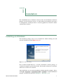
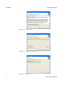
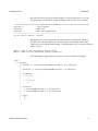
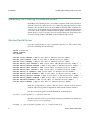
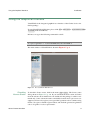
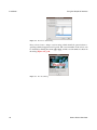
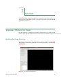
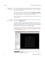
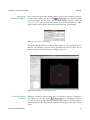
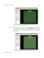
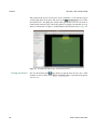
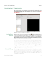
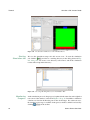
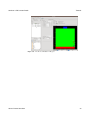
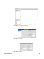
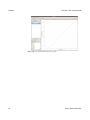
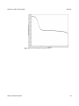
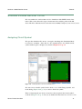
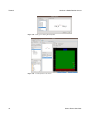
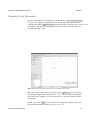
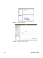
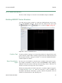
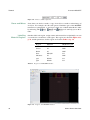
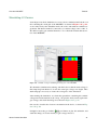
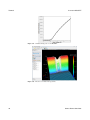
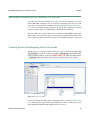
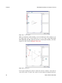
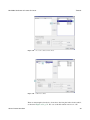
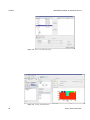
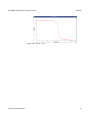
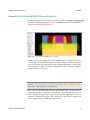
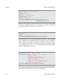
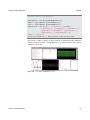
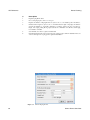
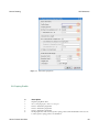
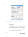
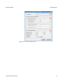
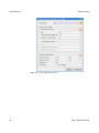
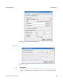
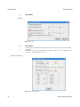
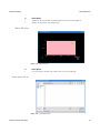
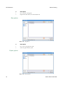
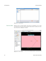
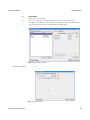
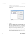
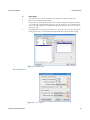
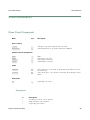
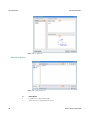
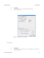
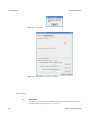
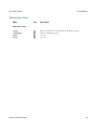
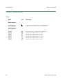
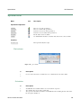
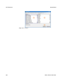
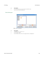
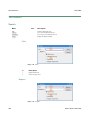
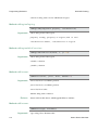
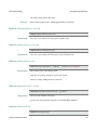
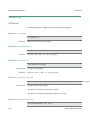
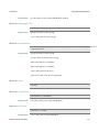
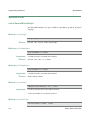
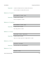
Simulate a PN Junction Diode
Tutorials
Figure 2.7 The Doping Profiles of the PN Junction Diode
Meshing
The numerical device simulation always relies on a mesh grid that divides the
device into many small elements. Click on the
Do Mesh tool, and accepts the
default parameters in the mesh parameter dialog. The initial mesh is shown in
Figure 2.8, p. 19. One may notice that the PN junction is slightly highlighted
with shading.
Figure 2.8 The Initial Mesh Grid of the PN Junction Diode
Genius Device Simulator
19