1
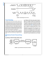
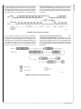
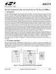
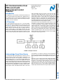
National Semiconductor
Application Note 2173
Dac Tran
July 14, 2011
Introduction
and/or transmitter. The bus consists of two wires, the SCL
(clock) line, and the SDA (data) line. The two wires are open
collector/drain outputs and must be pulled high using an external pull-up resistor. A logic state low is transmitted by
driving the output low. A logic high state is transmitted by releasing the output and allowing it to be pulled-up externally.
The appropriate pull-up resistor values will depend upon the
total bus capacitance and operating bus speed.
The I2C bus is a two-wire serial interface. These wires convey
information to and from devices connected to the bus, each
of which is identified by a unique address. Each device can
either transmit data or receive data. A device can operate as
either a master or as a slave; depending on whether it generates or receives the serial clock (SCL). A master initiates a
data transfer by addressing slave device and generates
START and STOP signals. The I2C protocol allows for more
than two devices to be connected to the bus and for multiple
master/slave relationships to exist.
This application note describes communication between devices using the FPD-Link III SerDes with a bidirectional control channel using I2C. The low latency bidirectional control
interface allows the master I2C device to remotely control peripherals across the serial link.
I2C Overview
The Inter-Integrated Circuit (I2C) bus is a two-wire bidirectional bus that allows multiple devices to operate on the same
bus (Figure 1). The bus consists of master and slave devices
which transmit data back and forth over the I2C interface.
Master devices control the bus and are typically microcontrollers, FPGAs, DSPs, or other digital controllers. The slave
devices are controlled by a host controller. I2C uses a masterslave protocol when data is exchanged among devices. Each
device on the bus (both master and slave) can be a receiver
30168801
FIGURE 1. Example of I2C Bus
Acknowledge From Slave Device
To communicate with a particular device on the bus, the controller (master) sends the slave address and listens for a
response from the slave. This response is referred to as an
“Acknowledge” (ACK = 1) or “No Acknowledge” (NACK = 0).
The Acknowledge cycle consists of two signals: the acknowledge clock pulse the master sends with each byte transferred,
and the acknowledge signal sent by the receiving device. All
bytes transmitted on the SDA line consists of eight bits of data
followed by an Acknowledge bit. Each byte transferred effectively requires 9 bits. The ACK bit allows data to be sent in
one direction to one device on the bus, and to indicate the
data was received. A device acknowledges a transfer of each
byte by pulling the SDA line low during the 9th clock pulse of
SCL.
ACKs also occur on the bus when data is being transmitted.
When the master is writing data, the slave ACKs after every
data byte is successfully received. When the master is reading data, the master ACKs after every data byte is received
to let the slave know it is ready to receive another data byte.
When the master wants to stop reading, it NACKs after the
last data byte and terminates with a stop condition on the bus.
I2C Communication Over FPD-Link III with Bidirectional Control Channel
I2C Communication Over
FPD-Link III with
Bidirectional Control
Channel
AN-2173
© 2011 National Semiconductor Corporation
301688
www.national.com
AN-2173
30168802
FIGURE 2. Acknowledge On The I2C Bus
an embedded a bidirectional control channel (referred as
BCC) concurrently over a single differential link. The BCC interface is I2C compliant according to the I2C standard. The
BCC interface provides access to programmable functions
and registers on the local and remote device(s). Three types
of operations are supported for I2C transactions with the bidirectional control channel SerDes chipsets: local, remote, and
remote slave as shown in Figure 3. Each device can function
as an I2C slave proxy or master proxy depending on the I2C
mode of operation. The SerDes interface acts as a virtual
bridge between host controller and the remote device. Local
operations use standard master to slave operations to the local Serializer or Deserializer. Local I2C operations do not
require any clock stretching by the slave and do not result in
transactions across the bidirectional control link. When addressing a remote peripheral or SerDes, the slave proxy will
forward any byte transactions sent by the Master controller to
the target device. The device will function as a master proxy
device; acts as a master on behalf of the I2C host controller.
Clock Stretching
In general, the I2C master controls the SCL clock line. This
line provides timing of all transfers on the bus. When the master is reading from the slave, the slave sends data on the SDA
line, but it is the master that controls the clock. However, there
are situations where a slave device(s) is not ready to respond
to the master or needs to slow down bus traffic. The I2C protocol defines a mode for the slave to hold the SCL line Low.
This mechanism is known as “Clock Stretching”. When the
slave receives the write/read command from the master it
holds the clock line Low. During any SCL low period, the slave
holds down SCL to prevent it from rising high again to delay
the SCL clock rate and pause communication.
When the master attempts to make SCL high to complete the
current clock pulse, it should verify that SCL has really gone
high. If it is still low, this indicates a slave is holding SCL low
and the master must wait until SCL goes high before continuing
Bidirectional Control Channel Using
I2C
The FPD-Link III Serializer/Deserializer (SerDes) chipsets
support full-duplex transmission of high-speed video data and
30168803
FIGURE 3. Typical FPD-Link III Connection with I2C Bus
www.national.com
2
CLOCK STRETCHING section. During this phase, the control
channel is embedded on the link and then data is reconstructed on the remote bus. Note the slave device will not control
the clock and only stretches it until the remote peripheral has
responded.
30168804
FIGURE 4. Clock Stretch For Sent Byte
Figure 4 shows an example of a remote access including the
clock stretching period following the transmitted byte, prior to
completion of the acknowledge bit. Since each byte transferred to the I2C slave must be acknowledged separately, the
clock stretching will be done for each byte sent by the host
controller. For remote accesses, the “Response Delay”
shown is on the order of 5 – 10 us and 10 – 15 us for
DS90UH925Q/UH926Q/UB925Q/UB926Q
and
DS90UB901Q/902Q/903Q/904Q respectively. The “Response Delay” includes the latency time of the control channel
packing and serialization protocol across the differential link
to the remote peripheral. The following diagrams (Figures 5,
6) show the timing relationships of the SCL clock and SDA
data signals.
30168805
FIGURE 5. Write Format To Remote I2C Slave
3
www.national.com
AN-2173
In order to communicate with remote devices on the I2C bus
through the bidirectional control channel, slave clock stretching must be supported by the I2C host controller. The chipsets
with a bidirectional control channel employ I2C clock stretching during remote data transmission; as described in the
AN-2173
30168806
FIGURE 6. Combined Format Read From Remote I2C Slave
approximate bit rate including latency timings across the control channel can be calculated by the following:
Data Throughput To Remote I2C
Slaves
9 bits / ((Host_bit * 9) + (Remote_bit * 9) + FCdelay + BCCdelay)
Since the BCC buffers each I2C data byte and regenerates
the I2C protocol on the remote side of the link, the overall I2C
throughput will be reduced. The reduction is dependent on the
operating frequencies of the local and remote interfaces. The
local I2C rate is based on the host controller clock rate, while
the remote rate depends on the settings for the proxy I2C
master (SCL frequency).
For purposes of understanding the effects of the BCC on data
throughput from a host controller to a remote I2C master, the
Example of DS90UH925Q/926Q/UB925Q/UB926Q chipset:
For the 100 kbit/s (100 kHz) :
Host_bit = 10us (100 kHz)
Remote_bit = 13.5us (default 74 kHz)
FCdelay = 1us (max)
BCCdelay = 9us (typical value)
Effective rate = 9bits / (90us + 121us + 1us + 9us) = 40.6 kbit/s
TABLE 1. Typical Achievable Bit Rates
FPD-Link III SerDes
Host I2C rate
Remote I2C Rate
Net bit rate
DS90UH925Q/926Q
DS90UB925Q/926Q
100 kbit/s
74 kbit/s (default settings)
40.6 kbit/s
100 kbit/s
100 kbit/s
47.4 kbit/s
400 kbit/s
100 kbit/s
73.5 kbit/s
400 kbit/s
400 kbit/s
163.6 kbit/s
100 kbit/s
100 kbit/s (default settings)
46.6 kbit/s
100 kbit/s
75 kbit/s
40.4 kbit/s
50 kbit/s
100 kbit/s
31.8 kbit/s
25 kit/s
100 kbit/s
19.4 kbit/s
DS90UB901Q/902Q
DS90UB903Q/904Q
Since the I2C protocol includes overhead for sending address
information as well as START and STOP bits, the actual data
throughput depends on the size and type of transactions
used. Use of large bursts to read and write data will result in
higher data transfer rates.
III chipsets with a bidirectional control channel and I2C peripherals.
References
1.
Conclusion
2.
3.
This application note provides an overview of the I2C bus
along with details describing the interface between FPD-Link
www.national.com
4
NXP UM102104, I2C-bus specification and user manual,
Rev. 03 - 19 June 2007
DS90UB901Q/902Q; DS90UB903Q/904Q Datasheet
DS90UH925Q/926Q, DS90UB925Q/926Q Datasheet
AN-2173
5
www.national.com
I2C Communication Over FPD-Link III with Bidirectional Control Channel
Notes
For more National Semiconductor product information and proven design tools, visit the following Web sites at:
www.national.com
Products
Design Support
Amplifiers
www.national.com/amplifiers
WEBENCH® Tools
www.national.com/webench
Audio
www.national.com/audio
App Notes
www.national.com/appnotes
Clock and Timing
www.national.com/timing
Reference Designs
www.national.com/refdesigns
Data Converters
www.national.com/adc
Samples
www.national.com/samples
Interface
www.national.com/interface
Eval Boards
www.national.com/evalboards
LVDS
www.national.com/lvds
Packaging
www.national.com/packaging
Power Management
www.national.com/power
Green Compliance
www.national.com/quality/green
Switching Regulators
www.national.com/switchers
Distributors
www.national.com/contacts
LDOs
www.national.com/ldo
Quality and Reliability
www.national.com/quality
LED Lighting
www.national.com/led
Feedback/Support
www.national.com/feedback
Voltage References
www.national.com/vref
Design Made Easy
www.national.com/easy
www.national.com/powerwise
Applications & Markets
www.national.com/solutions
Mil/Aero
www.national.com/milaero
PowerWise® Solutions
Serial Digital Interface (SDI) www.national.com/sdi
Temperature Sensors
www.national.com/tempsensors SolarMagic™
www.national.com/solarmagic
PLL/VCO
www.national.com/wireless
www.national.com/training
PowerWise® Design
University
THE CONTENTS OF THIS DOCUMENT ARE PROVIDED IN CONNECTION WITH NATIONAL SEMICONDUCTOR CORPORATION
(“NATIONAL”) PRODUCTS. NATIONAL MAKES NO REPRESENTATIONS OR WARRANTIES WITH RESPECT TO THE ACCURACY
OR COMPLETENESS OF THE CONTENTS OF THIS PUBLICATION AND RESERVES THE RIGHT TO MAKE CHANGES TO
SPECIFICATIONS AND PRODUCT DESCRIPTIONS AT ANY TIME WITHOUT NOTICE. NO LICENSE, WHETHER EXPRESS,
IMPLIED, ARISING BY ESTOPPEL OR OTHERWISE, TO ANY INTELLECTUAL PROPERTY RIGHTS IS GRANTED BY THIS
DOCUMENT.
TESTING AND OTHER QUALITY CONTROLS ARE USED TO THE EXTENT NATIONAL DEEMS NECESSARY TO SUPPORT
NATIONAL’S PRODUCT WARRANTY. EXCEPT WHERE MANDATED BY GOVERNMENT REQUIREMENTS, TESTING OF ALL
PARAMETERS OF EACH PRODUCT IS NOT NECESSARILY PERFORMED. NATIONAL ASSUMES NO LIABILITY FOR
APPLICATIONS ASSISTANCE OR BUYER PRODUCT DESIGN. BUYERS ARE RESPONSIBLE FOR THEIR PRODUCTS AND
APPLICATIONS USING NATIONAL COMPONENTS. PRIOR TO USING OR DISTRIBUTING ANY PRODUCTS THAT INCLUDE
NATIONAL COMPONENTS, BUYERS SHOULD PROVIDE ADEQUATE DESIGN, TESTING AND OPERATING SAFEGUARDS.
EXCEPT AS PROVIDED IN NATIONAL’S TERMS AND CONDITIONS OF SALE FOR SUCH PRODUCTS, NATIONAL ASSUMES NO
LIABILITY WHATSOEVER, AND NATIONAL DISCLAIMS ANY EXPRESS OR IMPLIED WARRANTY RELATING TO THE SALE
AND/OR USE OF NATIONAL PRODUCTS INCLUDING LIABILITY OR WARRANTIES RELATING TO FITNESS FOR A PARTICULAR
PURPOSE, MERCHANTABILITY, OR INFRINGEMENT OF ANY PATENT, COPYRIGHT OR OTHER INTELLECTUAL PROPERTY
RIGHT.
LIFE SUPPORT POLICY
NATIONAL’S PRODUCTS ARE NOT AUTHORIZED FOR USE AS CRITICAL COMPONENTS IN LIFE SUPPORT DEVICES OR
SYSTEMS WITHOUT THE EXPRESS PRIOR WRITTEN APPROVAL OF THE CHIEF EXECUTIVE OFFICER AND GENERAL
COUNSEL OF NATIONAL SEMICONDUCTOR CORPORATION. As used herein:
Life support devices or systems are devices which (a) are intended for surgical implant into the body, or (b) support or sustain life and
whose failure to perform when properly used in accordance with instructions for use provided in the labeling can be reasonably expected
to result in a significant injury to the user. A critical component is any component in a life support device or system whose failure to perform
can be reasonably expected to cause the failure of the life support device or system or to affect its safety or effectiveness.
National Semiconductor and the National Semiconductor logo are registered trademarks of National Semiconductor Corporation. All other
brand or product names may be trademarks or registered trademarks of their respective holders.
AN-2173
Copyright© 2011 National Semiconductor Corporation
For the most current product information visit us at www.national.com
National Semiconductor
Americas Technical
Support Center
Email: [email protected]
Tel: 1-800-272-9959
www.national.com
National Semiconductor Europe
Technical Support Center
Email: [email protected]
National Semiconductor Asia
Pacific Technical Support Center
Email: [email protected]
National Semiconductor Japan
Technical Support Center
Email: [email protected]