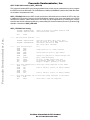
1
Order this document by: A N 1 2 3 3 / D
Freescale Semiconductor
Using M68HC16 Digital Signal Processing
To Build An Audio Frequency Analyzer
Freescale Semiconductor, Inc...
By Mark Glenewinkel
INTRODUCTION
This application note demonstrates the use of a microcontroller unit (MCU) with integrated DSP capabilities.
The MC68HC16Z1 is a high performance 16-bit MCU that includes on-chip peripheral modules and a CPU
module (CPU16). The CPU16 instruction set simplifies the use of digital signal processing algorithms, and
makes it easy to implement low-bandwidth filter and control-oriented applications.
OBJECTIVES
The goal of this application note is for an engineer to learn the MC68HC16Z1 well enough to design and
build an audio frequency analyzer (AFA). The following intermediate objectives have been defined to help
reach this goal.
• Learning the CPU16 instruction set
• Becoming familiar with MC68HC16Z1 modules
• Learning basic MCU I/O hardware and software
• Understanding DSP system concepts with the frequency analyzer
• Understanding and implementing common DSP algorithms with an MCU
This is a tutorial design project that follows a hands-on approach to using DSP. It provides concrete hardware/software applications that are used to understand and design an MCU-based system utilizing DSP al-
© Freescale Semiconductor, Inc., 2004. All rights reserved.
For More Information On This Product,
Go to: www.freescale.com
Freescale Semiconductor, Inc.
EQUIPMENT REQUIRED
The following items are needed to build and test the audio frequency analyzer (AFA).
1. An IBM PC compatible computer with a parallel printer port
2. The M68HC16Z1EVB
3. A prototyping or wire-wrap board
4. One straight DB25 cable, male on one end, female on the other
5. A 5 volt power supply
6. An audio sound source, preferably a CD player
7. Two Y-connectors to split the stereo sound source with audio cables
8. A sinusoidal waveform generator, optional
Freescale Semiconductor, Inc...
9. Oscilloscope for debugging, optional
All of the components needed to build the AFA are shown in Figure 4 and Figure 5, the AFA schematics.
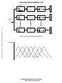
THE AUDIO FREQUENCY ANALYZER
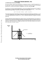
Spectral analysis is a method of determining the specific frequency content of a signal and the energy levels
of these frequencies. This information is processed by either Fourier Transform methods or by specific filtering of the signal. The information is tabulated for more analysis or displayed in a visual format.
One example of spectral analysis is found in oil exploration. An engineer sends a known signal into the earth
and then calculates the frequency content of the reflected signal. This is a classic input/output black box.
The transfer function of the black box (the earth in this case) yields clues to the structure beneath the surface. Different frequency responses correspond to different types of rock. With spectral analysis, the engineer can decide whether it is feasible to drill.
This project focuses on the frequency analysis of an audio signal. A frequency analyzer is often used in audio systems and recording studios. It filters out energy levels of specific audio frequencies and displays
them to indicate the frequency content of the audio signal. Audio frequency analyzers are also used in conjunction with equalizers to help the user define and shape the spectral characteristics of a sound source.
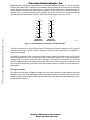
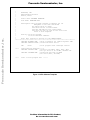
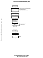
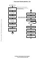
Figure 1 is a generic system diagram of a frequency analyzer based on bandpass filters. The input signal
is split and sent to all the filters. The filters pass only specific frequency components of the input signal. After
filtration, the strength of each passed signal is analyzed, and the amount of energy in each band is repre-
For More Information On This Product,
Go to: www.freescale.com
Freescale Semiconductor, Inc.
1ST BAND
BANDPASS FILTER
PEAK DETECT
&
COMPARISON
LED DRIVERS
PEAK DETECT
&
COMPARISON
LED DRIVERS
PEAK DETECT
&
COMPARISON
LED DRIVERS
2ND BAND
BANDPASS FILTER
Freescale Semiconductor, Inc...
ANALOG
SIGNAL
NTH BAND
BANDPASS FILTER
AN1233 F1
Figure 1 Frequency Analyzer System Diagram
MAGNITUDE
0dB
For More Information On This Product,
Go to: www.freescale.com
Freescale Semiconductor, Inc.
+5V
LOW-PASS ANTI-ALIASING
FILTER
STEREO SUMMING AMPLIFIER
HC16Z1
ADC
BIAS
0dB
LEFT
AD0
LED DRIVER
Freescale Semiconductor, Inc...
PCS0
SCK
MOSI
LED DRIVER
PCS0
EN
SCK
CLK
MOSI
DIN
DOUT
100 200
SCK
LED DRIVER
PCS0
EN
SCK
CLK
MOSI
DIN
DOUT
MOSI
FO
PCS0
RIGHT
1K 4K
EN
CLK
DIN
DOUT
10K
AN1233 F3
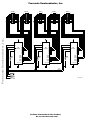
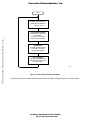
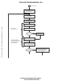
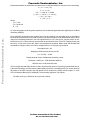
Figure 3 Audio Frequency Analyzer System Diagram
AFA Hardware
Familiarity with the AFA hardware helps to understand the code used to implement the analyzer. Figure 4
is a schematic of the analog front end of the AFA, and Figure 5 is a schematic of the display logic.
For More Information On This Product,
Go to: www.freescale.com
Freescale Semiconductor, Inc.
+5VA
AUDIO INPUT
R16
RIGHT
GND
C7
R14
R17, 90.9KΩ
R20, 665KΩ
2
4
6
INA
BPOA
LPIA
R18, 681KΩ
3
1
BPIA
LPOA
R19, 107KΩ
R22, 332KΩ
11
9
7
INB
BPOB
LPIB
R23, 332KΩ
10
12
BPIB
LPOB
C12
C10
R12
C13
C11
R13
4.7µF
4.7µF
0.1µF
0.1µF
R15
5
V+
17
V–
U9
MAX274
PCS0/SS
SCK
MOSI
LPID 19
21
BPOD
23
IND
R4, 196KΩ
22
47µF
R8, 453KΩ
R5, 40.2KΩ
13
LPOC
BPIC 15
R1, 232KΩ
LPIC 18
BPOC 15
INC 14
10KΩ
C4
AD0
R7, 200KΩ
BPID
0.1µF
GND
24
LPOD
C3
0.1µF
AGND
R2, 226KΩ
R3, 162KΩ
GND
20
+5VA
VCC
+5V
AGND
C2
0.1µF
AGND
FC
8
46.4KΩ
10KΩ
C1
10µF
+5VA
R21, 66.5KΩ
+5VA
10µH
C9
1.0µF
133KΩ
10µF
AGND
C8
133KΩ
10µF
LEFT
Freescale Semiconductor, Inc...
C6
VCC
L1
R6
1.0KΩ
2
4
6
8
10
12
14
16
18
20
1
3
5
7
9
11
13
15
17
19
P3
(MATES WITH P6 ON EVB)
VRHP
C5
0.1µF
AD0
GND
AGND
AD0
2
4
6
8
10
12
14
16
18
20
1
3
5
7
9
11
13
15
17
19
P2
(MATES WITH P7 ON EVB)
For More Information On This Product,
Go to: www.freescale.com
VRLP
AGND
AN1233 SCHEM P1
Freescale Semiconductor, Inc.
1
2
3
4
5
6
7
8
125 Hz
16
15
14
13
12
11
10
9
1
2
3
4
5
6
7
8
U1
U3
Freescale Semiconductor, Inc...
HLMP6658
12
11
10
8
R9
680Ω
DIN
CLK
EN
RX
500 Hz
16
15
14
13
12
11
10
9
HLMP6658
1
2
3
4
5
6
7
8
1 kHz
16
15
14
13
12
11
10
9
1
2
3
4
5
6
7
8
U4
4 kHz
16
15
14
13
12
11
10
9
1
2
3
4
5
6
7
8
U6
HLMP6658
10 kHz
16
15
14
13
12
11
10
9
U7
HLMP6658
HLMP6658
VCC
VCC
VCC
3
VDD
3
VDD
3
VDD
U2
12
MC14489
A
B
C
D
E
F
G
H
BANK1
BANK2
BANK3
BANK4
BANK5
VSS DOUT
14
7
6
5
4
2
1
20
19
9
13
15
16
17
18
11
10
8
R10
680Ω
DIN
CLK
EN
RX
U5
12
MC14489
A
B
C
D
E
F
G
H
BANK1
BANK2
BANK3
BANK4
BANK5
VSS DOUT
14
7
6
5
4
2
1
20
19
11
10
8
9
13
15
16
17
DIN
CLK
EN
RX
U8
MC14489
BANK1
BANK2
BANK3
BANK4
BANK5
R11
680Ω
18
A
B
C
D
E
F
G
H
VSS DOUT
14
CLOCK
ENABLE
7
6
5
4
2
1
20
19
9
13
15
16
17
18
GND
PCS0/SS
SCK
AN1233 SCHEM P2
MOSI
For More Information On This Product,
Go to: www.freescale.com
Freescale Semiconductor, Inc.
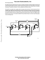
The Analog Front End
The analog front end contains all of the circuitry to condition the signal for analog-to-digital conversion and
subsequent digital signal processing. It consists of the summing circuitry for the stereo signal, the anti-aliasing filter, and the biasing circuitry for the ADC. A MAX274 low-pass filter chip, manufactured by the Maxim
Corporation of Sunnyvale, California, is used to implement all of these functions.
Freescale Semiconductor, Inc...
The MAX274 is an eighth order, programmable, continuous-time active filter. The chip consists of four independent cascadable second-order filter sections. Each filter section can implement any all-pole bandpass
or lowpass filter, characterized as a Butterworth, Bessel, or Chebyshev response. Each second-order section is programmable with four external resistors. A second-order section is illustrated in Figure 6. Maxim
provides an evaluation board and a software package that calculates resistor values from response specifications input by the user. This makes the MAX274 very flexible and easy to use when implementing highorder anti-aliasing filters.
BANDPASS
INPUT
RX
INPUT
IN
LOWPASS
OUTPUT
R2
50KΩ
79,575 PF
RY
79,575 PF
5KΩ
50KΩ
R1
R3
R4
BANDPASS
OUTPUT
AN1233 F6
For More Information On This Product,
Go to: www.freescale.com
Freescale Semiconductor, Inc.
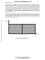
Anti-Aliasing Filter
When a signal of a given frequency is sampled at too low a rate, it appears as a totally different lower frequency at the output of the sampler. This phenomenon is referred to as aliasing. Aliasing occurs at a point
called the folding frequency, which is one-half the sampling frequency. In order for the frequency analyzer
to be accurate, sampling frequency must therefore be at least two times the highest frequency component
to be sampled. The ideal solution to this problem is to raise the sampling rate as high as possible, but realworld designs generally have a fixed upper limit on sampling frequency. The most practical solution is to
attenuate high frequency components of the input signal so that aliasing does not occur. The anti-aliasing
filter correctly attenuates the high frequency components of the signal, so that they are not present within
the sample bandwidth.
Freescale Semiconductor, Inc...
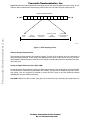
The AFA has a 25-kHz sampling frequency (Fs), and a processing bandwidth of 10 kHz. If no filter is used,
signal components with a frequency higher than 12.5 kHz alias at lower frequencies, and the digitized samples represent invalid information. Figure 7 shows these relationships. Fs/2 is the folding frequency, 12.5
kHz. Frequencies that will not alias with a 25 kHz sampling frequency are to the left of Fs/2, while frequencies that will alias are to the right of Fs/2.
MAGNITUDE
(dB)
0
10
12.5
FS/2
25
FS
FREQ
(kHz)
AN1233 F7
Figure 7 AFA Aliasing Without Filter
For More Information On This Product,
Go to: www.freescale.com
Freescale Semiconductor, Inc.
Voltage Attenuation (dB) = 20 ∗ log [1/(2ADCres)]
Where:
ADCres = A/D converter resolution
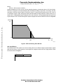
System bandwidth is 10 kHz, and at a 25 kHz sampling frequency, components above 12.5 kHz will alias.
Therefore, the signal must be attenuated 48 dB to eliminate all aliasing components. Accordingly, the filter
must have a minimum drop-off slope of 96 dB per octave. To insure that this requirement is met, a roll-off
of 100 dB per octave is used. Using these values with the MAX274 design software, resistor values for an
eighth order 0.5 dB passband ripple Chebyshev filter were obtained. Lower passband ripple was sacrificed
to gain steeper roll-off. The anti-aliasing filter response programmed into the MAX274 is shown in Figure 8.
MAGNITUDE
(dB)
Freescale Semiconductor, Inc...
0
-50
10
12.5
FS/2
15
25
FS
FREQ
(kHz)
AN1233 F8
Figure 8 AFA Anti-Aliasing Filter Roll-Off
ADC Input Biasing
The MC68HC16Z1 ADC module can convert analog data into six different digital representations. Digital
data can have 8-bit or 10-bit resolution, can be signed or unsigned, and can be left or right justified. These
formats are shown in Figure 9.
15
8 7
RESULT
0
For More Information On This Product,
Go to: www.freescale.com
Freescale Semiconductor, Inc.
Figure 10 shows hexadecimal representations of signed and unsigned ADC data. For 8-bit conversions,
there are 256 possible values. Unsigned formats assume the zero voltage point is at the low ADC reference
voltage, with 256 steps from low to high reference. Signed formats assume that the zero voltage point is
halfway between the low and high ADC reference voltages. The most significant bit indicates a positive or
negative value — 128 values represent positive voltages, and 128 two’s-complement values represent negative voltages ($00 represents the midpoint, and $FF represents midpoint minus one count).
Freescale Semiconductor, Inc...
$FF
5.0V
$7F
5.0V
$C0
$BF
3.75V
$40
$3F
3.75V
$80
$7F
2.5V
$00
$FF
2.5V
$40
$3F
1.25V
$C0
$BF
1.25V
$00
0V
UNSIGNED
HEXADECIMAL
REPRESENTATION
$80
0V
SIGNED
HEXADECIMAL
REPRESENTATION
AN1233 F10
Figure 10 Hexadecimal Representation of 8-Bit ADC Data
The AFA uses signed, 8-bit, left justified ADC data. The analog signal must be biased at 2.5 vdc, centered
between the 0 vdc and 5 vdc ADC reference voltages, in order to use this representation. The MAX274 is
used to bias the signal.
The MAX274 requires two power connections. Biasing circuitry consists of a voltage divider (R12, R13) and
decoupling capacitors (C10 – C13) connected to one of the MAX274 supplies. The V– pin is connected to
analog ground. The V+ pin is connected to the 5 volt supply. The GND pin is connected to 2.5 volts. This
splits the supply and causes the analog signal to have a 2.5 volt DC offset. The signal is buffered by an op
amp driver and is sent directly to the ADC module pins from the MAX274. The ADC can now properly sample the signal.
The Digital Back End
The digital back end shown in Figure 5 contains all of the circuitry required to output digitally processed
information to the LED array. When digital signal processing is complete, encoded energy levels for each
band are loaded into QSPI transmit RAM, then the QSPI is activated, and the data is transmitted serially to
the MC14489 LED drivers.
For More Information On This Product,
Go to: www.freescale.com
Freescale Semiconductor, Inc.
Three MC14489 drivers are used in the AFA. There are five 8-bit LED arrays. Two of the MC14489 chips
control four banks of four diodes each, and one controls two banks of four diodes each. Drive current for
diodes in each bank is supplied by pins A, B, C, and D of the MC14489. The cathodes of each bank of diodes are tied together and a bank-select pin sinks the current for that bank. Please refer to the MC14489
Data Sheet for more information.
The M68HC16Z1 EVB and Development Environment
The M68HC16Z1 Evaluation Board provides the capability to test and debug the audio frequency analyzer.
Table 1 shows development software supplied with the EVB.
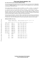
Table 1 Development Software
MASM16.EXE
Freescale Semiconductor, Inc...
MASM.EXE
HEX.EXE
MASM16.HLP
EVB16.EXE
MASM16 software is used to edit and assemble code, and EVB16 software is used to download code to the
EVB and run it. EVB16 software also has debug capabilities such as trace and breakpoint. Please refer to
the M68HC16Z1EVB User's Manual for a list of debug features.
Assembling the Development Environment
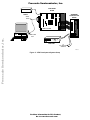
Assembling the development system with the AFA is simple. Hook up the system as shown in Figure 11.
The AFA project board connects to the M68HC16Z1EVB via P7 and P6. Use the DB25 cable to connect the
parallel port of the PC to the parallel port connector of the EVB. After connecting the 5 volt power supply to
the M68HC16Z1EVB, connect the audio signal source. A CD player is the recommended source for a high
quality output. Split the audio source outputs so that both the AFA board and the speakers receive the signals (audio splitters can be found at most stereo and electronics stores).
For More Information On This Product,
Go to: www.freescale.com
Freescale Semiconductor, Inc.
EVALUATION
BOARD
5-VOLT POWER
SUPPLY
ASSEMBLED
AFA PROTOTYPE
BOARD
SERIAL
CABLE
Freescale Semiconductor, Inc...
M68HC16Z1EVB
SERIAL COMM
PORT
❮ ■ ❯
❙❙
CD PLAYER
TO
LEFT AND RIGHT
SPEAKERS
AN1233 F9
Figure 11 AFA Development System Setup
For More Information On This Product,
Go to: www.freescale.com
Freescale Semiconductor, Inc.
AFA Software
Even though hardware is required to build the AFA, software running on the CPU16 performs most of the
actual work. Five tutorial programs must be integrated to complete the project. Each program demonstrates
specific functions of the AFA, and each is discussed in a separate section. Since this is a DSP project/tutorial, discussion focuses on signal-processing tasks. Each of the tutorial programs must be modified in order
to complete the AFA. The software steps to the AFA design are listed below.
1. Acquisition of data
2. QSPI to MC14489 interface
3. Periodic interrupt timer routine
4. Peak detector
5. 1-kHz bandpass filter routine
Freescale Semiconductor, Inc...
6. 5-band audio frequency analyzer
AFA software is listed in Table 2. Each of the first six programs in the table corresponds to one of the software steps listed above. In order to organize and streamline the project, each program has been designed
according to a standard template for the M68HC16Z1EVB. Figure 12 shows the template.
Table 2 AFA Project Software
ADC.ASM
QSPI_LED.ASM
INT_TEST.ASM
PEAK.ASM
1K_FLTR.ASM
5BAND_SA.ASM
EQUATES.ASM
ORG00000.ASM
INITSYS.ASM
INITRAM.ASM
OUTVAL1.ASM
OUTVAL2.ASM
OUTVAL1.ASM and OUTVAL2.ASM are lookup tables for the LED display routines. They contain values
that correspond to the number of LEDs needed to reflect a given peak value.
For More Information On This Product,
Go to: www.freescale.com
Freescale Semiconductor, Inc...
Freescale Semiconductor, Inc.
*
*
MOTOROLA, INC.
*
Advanced MCU Division
*
Austin, Texas
*
*
Title: HC16 SOFTWARE TEMPLATE
*
*
File Name: TEMPLATE.ASM
*
*
Description: This program provides a template for all
*
designers to use with the HC16Z1
*
An equate table is given.
*
The reset vector is initialized.
*
The CPU and RAM are also initialized.
*
The user can put his code in the ‘user area’
*
block of this template
*
*
History: 06/05/91 Created.
*
10/02/91 Modified comments.
*
*
Note: This program is written for the M68HC16Z1EVB.
***************************************************************************
INCLUDE ‘EQUATES.ASM’ ;table of EQUates for common register addr
INCLUDE ‘ORG00000.ASM’ ;initialize reset vector
ORG
$0200
;start program after interrupt vectors
*****
Initialization Routines *****
INCLUDE ‘INITSYS.ASM’ ;initially set EK=F, XK=0, YK=0, ZK=0
;set sys clock at 16.78 MHz, disable COP
INCLUDE ‘INITRAM.ASM’ ;initialize and turn on SRAM
;set stack (SK=1, SP=03FE)
*****
Start of user program area
*****
Figure 12 AFA Software Template
For More Information On This Product,
Go to: www.freescale.com
Freescale Semiconductor, Inc.
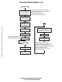
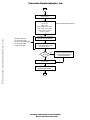
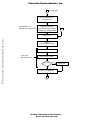
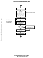
START
Freescale Semiconductor, Inc...
A/D DATA AQUISITION
INCOMING ANALOG SIGNAL WILL
BE CONTINUOUSLY SAMPLED AT
A RATE OF 24.95 kHz
DIGITAL SIGNAL PROCESSING
FIVE INFINITE IMPULSE RESPONSE
FILTERS WILL BE
EXECUTED ON EACH SAMPLE
WITHIN THE SAMPLING PERIOD
BAND ANALYSIS
EACH BAND MAGNITUDE WILL BE
UPDATED WITH THE LATEST
PROCESSED MAGNITUDE
QSPI → LED DISPLAY
THE DATA REPRESENTING EACH
BAND WILL BE SENT OUT TO THE
LED ARRAY VIA QSPI
AN1233 F13
Figure 13 AFA System Software Flowchart
All processing must be completed within one period of the 24.95-kHz sampling frequency. As shown below,
For More Information On This Product,
Go to: www.freescale.com
Freescale Semiconductor, Inc.
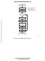
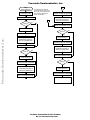
Figure 14 shows the relationship between sampling periods and real-time digital signal processing. All calculations and internal/external housekeeping must be taken care of within the given sample period.
Freescale Semiconductor, Inc...
STREAM OF SAMPLING PERIODS
GET ADC
VALUE
RUN 5 IIR
DSP ROUTINES
DETECT PEAK OF
EACH FILTER
WRITE PEAK VALUES
TO QSPI
TRANSMIT RAM
TURN ON QSPI
OUTPUT PEAK VALUES
TO LED ARRAY
668 SYSTEM CLOCK CYCLES
AN1233 F14
Figure 14 AFA Sampling Period
Software Design Implementation
The following sections examine AFA software in detail. For each of the programs, there is a discussion of
design and implementation, a code listing, and appropriate flow charts. In the interest of brevity, the standard template headers have been omitted from the listings, and redundant portions of flowcharts are reproduced only once.
Analog-to-Digital Data Acquisition (ADC.ASM)
In order to perform digital signal processing, a digital representation of the analog signal must be available.
The MC68HC16Z1 contains a programmable ADC module. The ADC has a number of automatic conversion modes. Only four registers are needed to control the ADC. Refer to the ADC Reference Manual
(ADCRM/AD) for more detailed information.
ADC.ASM initializes the ADC module, then goes into a continuous loop, repeating the programmed con-
For More Information On This Product,
Go to: www.freescale.com
Freescale Semiconductor, Inc.
ADC.ASM Code listing
INCLUDE 'EQUATES.ASM'
INCLUDE 'ORG00000.ASM'
ORG
*****
$0200
Initialization Routines
INCLUDE 'INITSYS.ASM'
INCLUDE 'INITRAM.ASM'
Freescale Semiconductor, Inc...
ORG
*****
*****
LOOP
SCFSET
$0200
ADC Initialization
LDD
#$0000
STD
ADCMCR
LDD
#$0003
STD
ADCTL0
ADC Start
LDD
#$0000
STD
ADCTL1
LDAA
BITA
BEQ
BRA
;table of EQUates for common register addr
;initialize reset vector
*****
;initially set EK=F, XK=0, YK=0, ZK=0
;set sys clock at 16.78 MHz, disable COP
;initialize and turn on SRAM
;set stack (SK=1, SP=03FE)
*****
;turn on ADC
;8-bit, set sample period
*****
;single 4 conversion, single channel, AD0
;writing to the ADCTL1 reg starts conversion
#$80
ADSTAT
SCFSET
LOOP
;check for the Sequence Complete Flag
;complete?, if not check again
;go get another sample
START
INCLUDE 'EQUATES.ASM'
INCLUDE 'ORG00000.ASM'
INCLUDE 'INITSYS.ASM'
INCLUDE 'INITRAM.ASM'
THESE INCLUDE FILES CONTAIN THE FOLLOWING:
AN EQUATE FILE WITH ALL THE Z1 REGISTERS DEFINED
RESET VECTOR INITIALIZATION
SYSTEM INITIALIZATION FOR THE Z1
INTERNAL RAM INITIALIZATION FOR THE Z1
ADC
INITIALIZATION
START UP
ADC
For More Information On This Product,
Go to: www.freescale.com
Freescale Semiconductor, Inc.
QSPI TO MC14489 Interface (QSPI_LED.ASM)
This program illustrates QSPI serial timing and data format, which must be understood in order to program
the QSPI to talk to the MC14489. The QSM Reference Manual (QSMRM/AD) and the MC14489 data sheet
are needed to understand the code.
QSPI_LED.ASM initializes the QSPI module and the three MC14489 drivers to handle 40 LEDs. After this
it updates the LED array by writing to the MC14489 display registers, then gives control back to the EVB16
development software. Values being sent to the array may be changed either by modifying the memory
locations that hold the transmitted data or by reassembling the lines that load these memory locations. Figure 16 is a flowchart of QSPI_LED.ASM.
QSPI_LED.ASM Code Listing
INCLUDE 'EQUATES.ASM'
INCLUDE 'ORG00000.ASM'
Freescale Semiconductor, Inc...
ORG
*****
$0200
Initialization Routines
INCLUDE 'INITSYS.ASM'
INCLUDE 'INITRAM.ASM'
*****
;table of EQUates for common register addr
;initialize reset vector
*****
;initially set EK=F, XK=0, YK=0, ZK=0
;set sys clock at 16.78 MHz, disable COP
;initialize and turn on SRAM
;set stack (SK=1, SP=03FE)
QSPI Initialization
LDAA
#$08
STAA
QPDR
LDAA
#$0F
STAA
QPAR
LDAA
#$FE
STAA
QDDR
*****
LDD
STD
LDD
STD
;mstr, womq=cpol=cpha=0
;16 bits, 2.10MHz serial baud rate
;no interrupt generated, no wrap mode
;newqp=0, endqp=3, queued for 4 trans
#$8004
SPCR0
#$0300
SPCR2
;output pcs0/ss* to 0 when asserted
;assign QSM port pins to qspi module
;assign all QSM pins as outputs except miso
*****
Fill QSPI Command.ram to write the config registers of the 14489
LDAA
#$C0
STAA
CR0
;cont=1, bitse=1, pcs0=0, no delays needed
STAA
CR1
STAA
CR2
LDAA
#$40
STAA
CR3
;cont=0, bitse=1, pcs0=0, no delays needed
*****
Fill QSPI Transmit.ram to write the config registers of the 14489
LDAA
#$3F
STD
TR0+1
;store $3F to tran.ram registers
For More Information On This Product,
Go to: www.freescale.com
Freescale Semiconductor, Inc.
*****
*****
Fill QSPI Transmit.ram for display registers of the 14489
The beginning LED values will be $00, all of the LEDs will be off
LDD
#$8000
;TR0 = $8000
STD
TR0
;TR1 = $0080
STAA
TR3+1
;TR2 = $0000
LDD
#$0080
;TR3 = $XX80
STD
TR1
;TR4 = $0000
CLRD
STD
TR2
STD
TR4
LDD
STD
*****
T125
T500
T1K
Freescale Semiconductor, Inc...
T4K
T10K
#$0400
SPCR2
;display registers need 5 transmissions
;newqp=0, endqp=4
Load up the various LED bands for experimentation
LDAA
#$0F
STAA
TR4+1
;125 Hz band
LDAA
#$3F
STAA
TR4
;500 Hz band
LDAA
#$FF
STAA
TR2+1
;1k Hz band
LDAA
#$3F
STAA
TR2
;4k Hz band
LDAA
#$03
STAA
TR1
;10k Hz band
LDD
STD
#$8404
SPCR1
BGND
BRA
;load up d
;turn on QSPI
;go back to EVB16 software
;reassemble code for T125 to T10K
;experiment with different values
T125
;branch back to TR125 line
For More Information On This Product,
Go to: www.freescale.com
Freescale Semiconductor, Inc.
START
INCLUDE 'EQUATES.ASM'
INCLUDE 'ORG00000.ASM'
INCLUDE 'INITSYS.ASM'
INCLUDE 'INITRAM.ASM'
THESE INCLUDE FILES CONTAIN THE FOLLOWING:
AN EQUATE FILE WITH ALL THE Z1 REGISTERS DEFINED
RESET VECTOR INITIALIZATION
SYSTEM INITIALIZATION FOR THE Z1
INTERNAL RAM INITIALIZATION FOR THE Z1
Freescale Semiconductor, Inc...
QSPI PORT INITIALIZATION
ASSIGN PORT PINS
TO OUTPUT QSPI SIGNALS
QSPI INITIALIZATION
MASTER MODE, 16 BIT
2.10 MHz SERIAL BAUD RATE
4 QUEUED TRANSMISSIONS
A
FILL QSPI COMMAND.RAM
FOR MC14489 CONFIG REGS
LOAD AND STORE VALUES TO
THE QSPI'S TRANSMIT.RAM TO
EXPERIMENT WITH THE LED ARRAY
FILL QSPI TRANSMIT.RAM
FOR MC14489 CONFIG REGS
TURN ON QSPI
TURN ON QSPI
ENTER BACKGROUND MODE
THIS FIRST TRANSFER INITIALIZES THE
INTERNAL CONFIGURATION REGISTERS
OF THE MC14489 TO HANDLE 40 LEDS
NO
SPIF BIT SET?
YES
FILL QSPI COMMAND.RAM
FOR MC14489 DISPLAY REGS
WHEN BACKGROUND MODE IS ENTERED,
CONTROL IS GIVEN BACK TO THE EVB16 SOFTWARE.
CHANGE THE VALUES THAT ARE LOADED AND
STORED INTO THE QSPI TRANSMIT.RAM TO EXPERIMENT
WITH THE LED ARRAY AND THE QSPI.
TO RUN THE ROUTINE AGAIN, TYPE GO IN THE
DEBUG WINDOW OF EVB16.
FILL QSPI TRANSMIT.RAM
FOR MC14489 DISPLAY REGS
For More Information On This Product,
Go to: www.freescale.com
Freescale Semiconductor, Inc.
The Periodic Interrupt Timer (INT_TEST.ASM)
The periodic interrupt timer (PIT) is an internal timer that can be programmed to make an interrupt service
request at specific intervals. One application of the PIT is to configure it to interrupt the processor every second so that an interrupt service routine can update a clock.
INT_TEST.ASM produces a square wave on the port F pins of the MC68HC16Z1. The square wave has a
set frequency determined by the PIT timeout period. The program uses the level six autovector and the PIT
times out at 15.6 ms. Port F is initialized for discrete output, then the code enters a wait loop until the programmed interval elapses. The interrupt service routine creates the square wave. Figure 17 is a flowchart
of INT_TEST.ASM.
For detailed information concerning interrupts, the PIT, and port F, refer to the MC68HC16Z1 User ’s Manual (MC68HC16Z1UM/D), the SIM Reference Manual (SIMRM/AD), and the CPU16 Reference Manual
(CPU16RM/AD).
Freescale Semiconductor, Inc...
INT_TEST.ASM Code Listing
*****
INCLUDE 'EQUATES.ASM'
INCLUDE 'ORG00000.ASM'
;table of EQUates for common register addr
;initialize reset vector
ORG
;start program after interrupt vectors
$0200
Initialization Routines
INCLUDE 'INITSYS.ASM'
INCLUDE 'INITRAM.ASM'
*****
;initially set EK=F, XK=0, YK=0, ZK=0
;set sys clock at 16.78 MHz, disable COP
;initialize and turn on SRAM
;set stack (SK=1, SP=03FE)
*****
Initialize level 6 autovector address
LDAB
#$00
TBEK
;ek extension pointer = bank0
LDD
#INT_RT
;load Dacc with interrupt vector addr
STD
$002C
;store addr to level 6 autovector
*****
Initialize PortF
LDAB
#$0F
TBEK
LDAB
#$00
STAB
PFPAR
LDAA
#$FF
STAA
DDRF
STAA
PORTF0
*****
Initialize the PIT
LDD
#$0616
STD
PICR
*****
*****
;ek extension pointer = bankf
;define port f as discrete i/o
;define port f as all output
;store $ff to port f
;pirql=6, piv=$16
For More Information On This Product,
Go to: www.freescale.com
Freescale Semiconductor, Inc.
START
INCLUDE 'EQUATES.ASM'
INCLUDE 'ORG00000.ASM'
INCLUDE 'INITSYS.ASM'
INCLUDE 'INITRAM.ASM'
THESE INCLUDE FILES CONTAIN THE FOLLOWING:
AN EQUATE FILE WITH ALL THE Z1 REGISTERS DEFINED
RESET VECTOR INITIALIZATION
SYSTEM INITIALIZATION FOR THE Z1
INTERNAL RAM INITIALIZATION FOR THE Z1
Freescale Semiconductor, Inc...
INITIALIZE LEVEL 6
AUTOVECTOR ADDRESS
INITIALIZE PORT F
DISCRETE OUTPUT ONLY
INITIALIZE PIT
REQUEST LEVEL 6
PIT VECTOR $16
15.6 mS INTERRUPT
NO OPERATION
INFINITE LOOP WAITING FOR
PIT INTERRUPT LEVEL 6
START
LEVEL 6 INTERRUPT
STACK D, C, AND K REG
ONE'S COMPLEMENT
PORT F
CREATES A SQUARE WAVE
ON PORT F
For More Information On This Product,
Go to: www.freescale.com
Freescale Semiconductor, Inc.
Signal Peak Detector (PEAK.ASM)
The signal peak detector graphically measures and displays the peak amplitude of a signal in real time. An
audio signal is sampled at 24.95 kHz. The peak amplitude of the signal is detected, then a value that represents the peak on a bar of eight light-emitting diodes (LED) is generated. A reference value of 0.775 Vrms
equivalent to 0 dB is used to relate the digital peak value to the LED display. The LED bar can display a
signal in the range –15 dB to +6 dB, in 3 dB steps. Figure 18 shows relationships between the LED bar,
decibels, Vrms, and Vp. Figure 19 shows the relationship between an analog input signal and the peak values displayed. Figure 20 is a flowchart of PEAK.ASM.
Freescale Semiconductor, Inc...
LED BAR
dB
VRMS
VPEAK
+6
1.548
2.187
+3
1.096
1.548
0
0.775
1.096
-3
0.549
0.775
-6
0.389
0.549
-9
0.275
0.389
-12
0.195
0.275
-15
0.138
0.195
Vin
dB = 20 • log ------------
Vref
0dB ≥ Vref = 0.775Vrms
Vpeak =
2 • Vrms
AN1233 F18
For More Information On This Product,
Go to: www.freescale.com
Freescale Semiconductor, Inc.
The code originating in the internal RAM will now be correctly loaded into the MC68HC16Z1.
PEAK.ASM reads values from a look-up table in memory. The file OUTVAL2.ASM contains the table. Be
sure this file is in the same directory as PEAK.ASM before assembly.
2.5
2.187
VOLTS
1.548
1.096
Freescale Semiconductor, Inc...
0.776
0.0
0.549
0.389
0.275
0.195
- 0.195
- 0.275
- 0.389
- 0.549
TIME
- 0.776
- 1.096
- 1.548
- 2.187
- 2.5
AN1233 F19
Figure 19 Analog Input vs Peak Display Level
After initializing the SRAM, the ADC, the QSPI, and the PIT, the code jumps to internal RAM at location
For More Information On This Product,
Go to: www.freescale.com
Freescale Semiconductor, Inc.
Using a PIT interrupt to decrement the peak value causes the LED display to decrease slowly, like a capacitor discharging, when the input signal decreases rapidly. This gives the display a more fluid appearance
when rapidly-changing peak values are measured. If the display jumped from peak to peak, the discontinuity
would lower the aesthetic appeal. In fact, most commercial audio analyzers show the relative peak differences of the frequency spectrum rather than attempt to display the peak signal precisely.
To test the code, hook up the system as shown in Figure 11. Input a known signal and observe the display.
Apply an audio signal from the sound source and watch the peak detector execute in real time. If there is
only one sound source output, connect it to either the left or right AFA input. The display is calibrated to the
output of a CD player. The CD player puts out a line level signal, with .775 Vrms equal to 0 dB. If the sound
source is not a CD player, adjust the output of the sound source so that the dynamic range of the signal is
fully displayed.
PEAK.ASM Code Listing
Freescale Semiconductor, Inc...
INCLUDE 'EQUATES.ASM'
INCLUDE 'ORG00000.ASM'
*****
PK
CNT
Temporary variable storage
EQU
$0200
; bank F
EQU
$0201
; bank F
ORG
*****
;table of EQUates for common register addr
;initialize reset vector
$0200
Initialization Routines *****
INCLUDE 'INITSYS.ASM'
;initially set EK=F, XK=0, YK=0, ZK=0
;set sys clock at 16.78 MHz, disable COP
*****
RAM and
LDD
STD
LDD
STD
CLR
LDAB
TBSK
LDS
Stack Initialization
#$00FF
RAMBAH
;store high ram array, bank F
#$0000
RAMBAL
;store low ram array, 0000
RAMMCR
;enable ram
#$0F
;set SK to bank F for system stack
#$02FE
;put SP in 1k internal SRAM
*****
Initialize level 6 autovector address
LDAB
#$00
TBEK
;ek extension pointer = bank0
LDD
#JMPINT
;load Dacc with interrupt vector addr
STD
$002C
;store addr to level 6 autovector
*****
Initialize the PIT
LDAB
#$0F
TBEK
LDD
#$0616
*****
;ek extension pointer = bankf
For More Information On This Product,
Go to: www.freescale.com
Freescale Semiconductor, Inc.
STAA
STAA
LDAA
STAA
*****
*****
*****
GO
SPIWT
Freescale Semiconductor, Inc...
*****
*****
*****
*****
*****
;cont=0, bitse=1, pcs0=0, no delays needed
Fill QSPI Transmit.ram to write the config registers of the 14489
LDAA
#$3F
STD
TR0+1
;store $3F to tran.ram registers
STD
TR2
STD
TR3+1
Turn on the QSPI, this will write to the config registers
of the MC14489 drivers
LDD
#$8404
STAA
SPCR1
;turn on spi
LDAA
SPSR
;after sending data we wait until the
ANDA
#$80
;spif bit is set, before we can send more
CMPA
#$80
;check for spi done
BNE
SPIWT
Fill QSPI Command.ram to write the display registers
LDAA
#$C0
STAA
CR0
;cont=1, bitse=1, pcs0=0, no
STAA
CR1
LDAA
#$40
;cont=0, bitse=1, pcs0=0, no
STAA
CR2
STAA
CR4
LDAA
#$80
;cont=1, bitse=0, pcs0=0, no
STAA
CR3
of the 14489
delays needed
delays needed
delays needed
Fill QSPI Transmit.ram for display registers of the 14489
The beginning LED values will be $00, all of the LEDs will be off
LDD
#$8000
STD
TR0
;TR0 = $8000
STAA
TR3+1
;TR1 = $0080
LDD
#$0080
;TR2 = $0000
STD
TR1
;TR3 = $XX80
CLRD
;TR4 = $0000
STD
TR2
STD
TR4
LDD
STD
*****
CR1
CR2
#$40
CR3
#$0400
SPCR2
;display registers need 5 transmissions
;newqp=0, endqp=4
ADC Initialization
LDD
#$0000
STD
ADCMCR
LDD
#$0003
STD
ADCTL0
*****
;turn on ADC
;8-bit, set sample period
Initialize the extension registers for the internal ram in bank F
Set up the extension registers to point to bank F
LDAB
#$0F
;load b with $0F
TBEK
;transfer Bacc to Ek
TBXK
;transfer Bacc to Xk
For More Information On This Product,
Go to: www.freescale.com
Freescale Semiconductor, Inc.
LDD
STD
*
TRAN
Freescale Semiconductor, Inc...
LD
#$8404
SPCR1
; 6 load up d
; 6 turn on QSPI, send LED data out
Get LED encode value from look-up table
TED
; 2 transfer Eacc to Dacc
STAA
LD+3
; 6 Dacc high byte -> instruction ldaa $03??
NOP
; 2 no operation, wait for CPU pipeline
NOP
; 2 no operation, wait for CPU pipeline
LDAA
LED_TBL
; 6 load Aacc with the encoded LED value
;
from scaled peak LED table
*
Update peak value if needed
CMPA
PK
; 6 compare value to previous peak value
BLS
DN
; 6,2 branch if not more than peak value
STAA
PK
; 6 store new peak value
STAA
TR1
; 6 store new value to all 5 qspi tran.rams
STAA
TR2
; 6
STAA
TR2+1
; 6
STAA
TR4
; 6
STAA
TR4+1
; 6
*****
*****
*****
Loop to generate calculated delay
Clocks = 6 + 8*(N-1) N >= 1
N is the number put into the B accumulator
DN
WAIT
LDAB
DECB
BNE
#$4B
WAIT
; 75dec this loop will create an extra delay
; to make a 24.95kHz sampling rate
; or a 668 cycle sampling period
; 598 cycles
JMP
LP
; 6 jump back to start another conversion
*****
*****
*****
INT_RT
DONE
Exceptions/Interrupts
*****
This interrupt is used to decrement each LED bar value
representing the peak value of the audio signal
PSHM
D,CCR
;stack Dacc and CCR on stack
LDAA
PK
;load Aacc with peak value
BEQ
DONE
;equal to 0?, then done
ANDP
RORA
STAA
STAA
STAA
STAA
STAA
STAA
LDD
STD
#$FEFF
PULM
RTI
D,CCR
TR1
TR2
TR2+1
TR4
TR4+1
PK
#$8404
SPCR1
;clear C bit
;rotate right once, decrease peak value
;store Aacc to all qspi tran.ram
;store Aacc to peak value
;load up Dacc
;turn on QSPI, send LED data out
;pull Dacc and CCR from stack
;return from interrupt
For More Information On This Product,
Go to: www.freescale.com
Freescale Semiconductor, Inc.
START
INCLUDE 'EQUATES.ASM'
INCLUDE 'ORG00000.ASM'
INCLUDE 'INITSYS.ASM'
THESE INCLUDE FILES CONTAIN THE FOLLOWING:
AN EQUATE FILE WITH ALL THE Z1 REGISTERS DEFINED
RESET VECTOR INITIALIZATION
SYSTEM INITIALIZATION FOR THE Z1
INITIALIZE INTERNAL RAM
AT LOCATION $F0000
STACK AT $F02FE
Freescale Semiconductor, Inc...
INITIALIZE LEVEL 6
AUTOVECTOR ADDRESS
INITIALIZE PIT
REQUEST LEVEL 6
PIT VECTOR $16
15.6 mS INTERRUPT
A
FILL QSPI COMMAND.RAM
FOR MC14489 CONFIG REGS
THIS FIRST TRANSFER INITIALIZES THE
INTERNAL CONFIGURATION REGISTERS
OF THE MC14489 TO HANDLE 40 LEDS
FILL QSPI TRANSMIT.RAM
FOR MC14489 CONFIG REGS
TURN ON QSPI
SPIF BIT SET?
QSPI PORT INITIALIZATION
ASSIGN PORT PINS
TO OUTPUT QSPI SIGNALS
QSPI INITIALIZATION
MASTER MODE, 16 BIT
2.10 MHz SERIAL BAUD RATE
4 QUEUED TRANSMISSIONS
A
NO
YES
FILL QSPI COMMAND.RAM
FOR MC14489 DISPLAY REGS
FILL QSPI TRANSMIT.RAM
FOR MC14489 DISPLAY REGS
CHANGE QSPI TO 5
QUEUED TRANSMISSIONS
ADC
INITIALIZATION
For More Information On This Product,
Go to: www.freescale.com
Freescale Semiconductor, Inc.
B
LOCATION $F0000
CLEAR LED UPDATE COUNTER
CLEAR PEAK VALUE
START THE ADC
Freescale Semiconductor, Inc...
READ ADC VALUE
READ LED UPDATE COUNTER
CHECK IF LEDS
NEED TO BE UPDATED
ADD 1 TO LED COUNTER
256 CYCLES?
YES
TURN ON QSPI
NO
THE ADC VALUE IS USED
AS THE OFFSET WHEN READING
THE LED ENCODE VALUE
FROM THE LED TABLE
STORE ADC VALUE TO THE
READ LED TABLE INSTRUCTION
READ LED ENCODE PEAK VALUE
FROM THE LED TABLE OFFSET
BY THE ADC VALUE
PEAK >
OLD PEAK?
NO
YES
STORE AWAY NEW ENCODED PEAK
STORE NEW ENCODED PEAK
TO QSPI TRANSMIT.RAM
For More Information On This Product,
Go to: www.freescale.com
Freescale Semiconductor, Inc.
A 1-kHz Bandpass Filter (1K_FLTR.ASM)
This code is similar in function to the peak detector, except that it executes a 1-kHz IIR bandpass filter on
the input signal. The peak is detected and displayed on an LED bar in real time. The focus is on using the
MC68HC16Z1 to implement the digital filter. Figure 22 is a flowchart of 1K_FLTR.ASM.
The objective is to take incoming sampled data x(n), and run the bandpass filter function on the sample to
produce output y(n). Again, this is the basic ‘black box’ concept of electrical engineering — excite the input
and watch the output change. The function in the ‘black box’ is defined below.
y(n) = 2 ∗ {α ∗ [x(n) − x(n−2)] + γ ∗ y(n-1) − β ∗ y(n−2)}
Freescale Semiconductor, Inc...
This function implements an IIR bandpass function with characteristics defined by the coefficients α, β, and
γ. In an RLC bandpass filter circuit, resistors, capacitors, and inductors would characterize filter response.
In the digital implementation of the filter, the α, β, and γ coefficients determine the response in much the
same way.
The basic parameters that define digital filter response are the Q, the sampling frequency (Fs), and the center frequency (Fo). The Q value defines the sharpness of the filter and is equal to the center frequency divided by the bandwidth between the 3 dB points. The specified sampling frequency is 24.95 kHz, the center
frequency is 1 kHz, and Q value is 1.5. Figure 21 illustrates these relationships. Table 3 shows the way in
which coefficients are stored in memory.
MAGNITUDE
(DB)
0
3dB BANDWIDTH
-3
Fo
Q = ------------------------------------BANDWIDTH
FO
For More Information On This Product,
Go to: www.freescale.com
FS
FREQ
Freescale Semiconductor, Inc.
Equations that define the coefficients are shown below. Coefficient values are also given in the code listing.
θ = {(2 ∗ π ∗ Fo) / Fs}
X = θ / (2 ∗ Q)
If X > π / 4 then X = 0.75398
β = 0.5 ∗{1 − tan (X)} / {1+ tan (X)}
γ = (0.5 + β) ∗ cos θ
α = (0.5 − β) / 2
Where:
Fo = 1 kHz
Fs = 24.95 kHz
Q = 1.5
Freescale Semiconductor, Inc...
For more information concerning these equations, refer to Motorola Application Note Digital Stereo 10-Band
Generator (APR2/D).
Once coefficient values have been obtained, they must be encoded. The assembler does not understand
fractional decimal numbers, so fractional values are converted into signed 16-bit hexadecimal values. When
using two’s complement arithmetic, the most significant bit (bit 15) is the sign bit, and the fraction is contained in bits 14 to 0. Fifteen bits can represent the decimal numbers from 0 to 32,767. Multiply the decimal
fraction by 32,768, then convert the value to the hexadecimal equivalent. Make certain that hexadecimal
equivalents of negative values are in two’s complement form. An example is given below.
Decimal fraction = 0.5
Multiply fractional decimal value by 32,768
0.5 ∗ 32,768 = 16,384
Change decimal value to hexadecimal and binary values
16,384 dec = 4000 hex = 0100 0000 0000 0000 bin
4000 hex is the 16-bit fractional value.
CPU16 multiply and add instructions are used to implement the function. Processing is streamlined so that,
in the final AFA design, five filters can be implemented in the 40.08 µs sampling period. For a more thorough
discussion of the DSP instruction set and related CPU16 architecture, please consult Chapter 11 in the
CPU16 Reference Manual (CPU16RM/AD). The processing sequence is as follows.
The ADC value x(n) is divided by two to prevent overflow.
For More Information On This Product,
Go to: www.freescale.com
Freescale Semiconductor, Inc.
As mentioned earlier, the 1-kHz bandpass filter is very similar to the peak detector design. Once the DSP
is finished on the input x(n) sample, the peak detect algorithm is executed.
The include file OUTVAL1.ASM is used to encode the DSP output with an LED display value multiplied by
two. Be sure this file is in the same directory as 1K_FLTR.ASM during assembly.
The best way to test this program is to connect a signal generator with sine-wave sweep capability to the
AFA inputs, then set it to sweep from 0 to 15 kHz. The 1-kHz LED bar should display the amplitude of a pure
1-kHz tone and the routine should filter out higher and lower frequency signals. Since Q is equal to 1.5,
some side-lobe frequencies in the pass band should be evident. For instance, if a 2-kHz pure signal is sent
into the filter, the side-lobe response of the 1-kHz bandpass will pass an attenuated level of the 2-kHz tone.
1K_FLTR.ASM Code Listing
Freescale Semiconductor, Inc...
INCLUDE 'EQUATES.ASM'
INCLUDE 'ORG00000.ASM'
;table of EQUates for common register addr
;initialize reset vector
*****
COEFBS
GAM_1K
BETA_1K
ALPH_1K
Addresses of coefficients for the IIR Filters and initialization
EQU
$0280
;base addr of coefficients
EQU
COEFBS+$0
;addr of the gamma coef
EQU
COEFBS+$2
;addr of the beta coef
EQU
COEFBS+$4
;addr of the alpha coef
ORG
$F0280
dc.w
$7257
;1k Hz gamma coef, Q=1.5
dc.w
$C9F0
;1k Hz beta coef, Q=1.5
dc.w
$04F7
;1k Hz alpha coef, Q=1.5
*****
XTRMBS
XN1_1K
XN2_1K
Addresses of filter terms for the x(n) terms and initialization
EQU
$02A0
;base addr of x(n) filter terms
EQU
XTRMBS+$0
;x(n-1)
EQU
XTRMBS+$2
;x(n-2)
ORG
$F02A0
dc.w
$0000
;1k Hz x(n-1)
dc.w
$0000
;1k Hz x(n-2)
*****
YTRMBS
YN1_1K
YN2_1K
X_2_1K
Addresses of filter terms for the y(n) terms and initialization
EQU
$02C0
;base addr of y(n) filter terms
EQU
YTRMBS+$0
;y(n-1)
EQU
YTRMBS+$2
;y(n-2)
EQU
YTRMBS+$4
;x(n) - x(n-2), stored here for mac
ORG
$F02C0
dc.w
$0000
;1k y(n-1)
dc.w
$0000
;1k y(n-2)
dc.w
$0000
;1k [ x(n) - x(n-2) ]
*****
PKRES
PK_1K
CNT
Addresses of various temporary variables and initialization
EQU
$02E0
;base addr of filter result storage
EQU
PKRES+$0
;peak value for 1k Hz
EQU
PKRES+$1
;count value for LED qspi update routine
For More Information On This Product,
Go to: www.freescale.com
Freescale Semiconductor, Inc...
Freescale Semiconductor, Inc.
*****
RAM and
LDD
STD
LDD
STD
CLR
LDAB
TBSK
LDS
*****
Initialize level 6 autovector address
LDAB
#$00
TBEK
;ek extension pointer = bank0
LDD
#JMPINT
;load Dacc with interrupt vector addr
STD
$002C
;store addr to level 6 autovector
*****
Initialize the PIT
LDAB
#$0F
TBEK
LDD
#$0616
STD
PICR
LDD
#$0101
STD
PITR
ANDP
#$FF1F
*****
QSPI Initialization
LDAA
#$08
STAA
QPDR
LDAA
#$0F
STAA
QPAR
LDAA
#$FE
STAA
QDDR
*****
LDD
STD
LDD
STD
;mstr, womq=cpol=cpha=0
;16 bits, 2.10MHz serial baud rate
;no interrupt generated, no wrap mode
;newqp=0, endqp=3, queued for 4 trans
*****
Stack Initialization
#$00FF
RAMBAH
;store high ram array, bank F
#$0000
RAMBAL
;store low ram array, 0000
RAMMCR
;enable ram
#$0F
;set SK to bank F for system stack
#$02FE
;put SP in 1k internal SRAM
#$8004
SPCR0
#$0300
SPCR2
;ek extension pointer = bankf
;pirql=6, piv=$16
;set the periodic timer at 62.5msec
;set interrupt priority to 000
;output pcs0/ss* to 0 when asserted
;assign QSM port pins to qspi module
;assign all QSM pins as outputs except miso
*****
Fill QSPI Command.ram to write the config registers of the 14489
LDAA
#$C0
STAA
CR0
;cont=1, bitse=1, pcs0=0, no delays needed
STAA
CR1
STAA
CR2
LDAA
#$40
STAA
CR3
;cont=0, bitse=1, pcs0=0, no delays needed
*****
Fill QSPI Transmit.ram to write the config registers of the 14489
LDAA
#$3F
STD
TR0+1
;store $3F to tran.ram registers
STD
TR2
STD
TR3+1
*****
*****
Turn on the QSPI, this will write to the config registers
of the MC14489 drivers
For More Information On This Product,
Go to: www.freescale.com
Freescale Semiconductor, Inc.
*****
*****
Fill QSPI Transmit.ram for display registers of the 14489
The beginning LED values will be $00, all of the LEDs will be off
LDD
#$8000
STD
TR0
;TR0 = $8000
STAA
TR3+1
;TR1 = $0080
LDD
#$0080
;TR2 = $0000
STD
TR1
;TR3 = $XX80
CLRD
;TR4 = $0000
STD
TR2
STD
TR4
LDD
STD
Freescale Semiconductor, Inc...
*****
#$0400
SPCR2
;display registers need 5 transmissions
;newqp=0, endqp=4
ADC Initialization
LDD
#$0000
STD
ADCMCR
LDD
#$0003
STD
ADCTL0
*****
;turn on ADC
;8-bit, set sample period
*****
*****
Initialize the extension registers for the internal ram in bank F
Set up the extension registers to point to bank F
LDAB
#$0F
;load b with $0F
TBEK
;transfer Bacc to Ek
TBXK
;transfer Bacc to Xk
TBYK
;transfer Bacc to Yk
TBZK
;transfer Bacc to Zk
JMP
RAM
;jump to internal ram for speed!
*****
Start of Internal 1K RAM
ORG
$F0000
CLR
CNT
;clear LED update counter
CLR
PK_1K
;clear 1K peak value
RAM
*
LP
Initialization for DSP
ORP
#$0010
CLRD
TDMSK
LDY
#COEFBS
LDX
#YTRMBS
;set saturation mode for Macc
;clear Dacc
;no modulo addressing
;load y with the coef base addr
;load x with the yterm base addr
CLRD
STD
; 2 clear Dacc
; 6 single 4 conversion, single channel AD0
;
writing to the ADCTL1 reg starts conv
ADCTL1
*
Divide input x(n) by 2, no overflow problem
LDAA
LJSRR0
; 6 load Aacc with left jus signed ADC value
ASRA
; 2 divide by 2
STAA
AD
; 6 store divide by 2 adc value away
*
Check if LEDs need updating
LDAA
CNT
; 6 load Aacc with count
ADDA
#1
; 2 add 1 to Aacc
STAA
CNT
; 6 store new count
For More Information On This Product,
Go to: www.freescale.com
Freescale Semiconductor, Inc.
*
*
Freescale Semiconductor, Inc...
LD1K
Digital
TED
SUBD
STD
LDD
STED
processing algorithm
; 2 transfer Eacc to Dacc
XN2_1K
; 6 Dacc = x(n) - x(n-2)
X_2_1K
; 6 store Dacc to [x(n) - x(n-2)] addr
XN1_1K
; 6 load Dacc with x(n-1)
XN1_1K
; 8 store x(n) to x(n-1) and
;
store x(n-1) to x(n-2)
MAC
MAC
MAC
TMET
ASLE
2,2
2,2
-4,-4
;12
;12
;12
; 2
; 2
gamma*(yn1)+Macc=Macc
beta*(yn2)+Macc=Macc
alpha*[x(n)-x(n-2)]+Macc=Macc
transfer Macc to Eacc, truncate
multiply Eacc by 2
Get LED encode value from look-up table
TED
; 2 transfer Eacc to Dacc
STAA
LD1K+3
; 6 Dacc high byte -> instruction ldaa $03??
NOP
; 2 no operation, due to CPU pipeline
NOP
; 2 no operation, due to CPU pipeline
LDAA
LED_TBL
; 6 load Aacc with the encoded LED value
;
from scaled peak LED table
*
Update peak value if needed
CMPA
PK_1K
; 6 compare value to previous peak value
BLS
DN1K
; 6,2 branch if not more than peak value
STAA
PK_1K
; 6 store new peak value
STAA
TR2+1
; 6 store new value to 1k qspi tran.ram
*
DN1K
Update y(n-1) and y(n-2)
LDD
YN1_1K
; 6 load Dacc with y(n-1)
STED
YN1_1K
; 8 store Eacc to y(n-1), Dacc to y(n-2)
*****
*****
*****
Loop to generate calculated delay
Clocks = 6 + 8*(N-1) N >= 1
N is the number put into the B accumulator
WAIT
LDAB
DECB
BNE
NOP
NOP
NOP
JMP
*****
*****
*****
INT_RT
#$3D
WAIT
LP
;
;
;
;
;
;
;
;
61 this loop will create an extra delay
to make a 24.95kHz sampling rate
or a 668 cycle sampling period
486 cycles
2
2
2
6 jump back to start another conversion
Exceptions/Interrupts
*****
This interrupt is used to decrement the LED bar value
representing the peak value of the 1k filter band
PSHM
D,CCR
;stack Dacc and CCR on stack
LDAA
PK_1K
;load Aacc with 1K peak value
BEQ
DONE
;equal to 0?, then done
ANDP
#$FEFF
;clear C bit
For More Information On This Product,
Go to: www.freescale.com
Freescale Semiconductor, Inc.
START
INCLUDE 'EQUATES.ASM'
INCLUDE 'ORG00000.ASM'
INCLUDE 'INITSYS.ASM'
THESE INCLUDE FILES CONTAIN THE FOLLOWING:
AN EQUATE FILE WITH ALL THE Z1 REGISTERS DEFINED
RESET VECTOR INITIALIZATION
SYSTEM INITIALIZATION FOR THE Z1
INITIALIZE INTERNAL RAM
AT LOCATION $F0000
STACK AT $F02FE
Freescale Semiconductor, Inc...
INITIALIZE LEVEL 6
AUTOVECTOR ADDRESS
INITIALIZE PIT
REQUEST LEVEL 6
PIT VECTOR $16
15.6 mS INTERRUPT
A
FILL QSPI COMMAND.RAM
FOR MC14489 CONFIG REGS
THIS FIRST TRANSFER INITIALIZES THE
INTERNAL CONFIGURATION REGISTERS
OF THE MC14489 TO HANDLE 40 LEDS
FILL QSPI TRANSMIT.RAM
FOR MC14489 CONFIG REGS
TURN ON QSPI
SPIF BIT SET?
QSPI PORT INITIALIZATION
ASSIGN PORT PINS
TO OUTPUT QSPI SIGNALS
QSPI INITIALIZATION
MASTER MODE, 16 BIT
2.10 MHz SERIAL BAUD RATE
4 QUEUED TRANSMISSIONS
A
NO
YES
FILL QSPI COMMAND.RAM
FOR MC14489 DISPLAY REGS
FILL QSPI TRANSMIT.RAM
FOR MC14489 DISPLAY REGS
CHANGE QSPI TO 5
QUEUED TRANSMISSIONS
ADC
INITIALIZATION
For More Information On This Product,
Go to: www.freescale.com
Freescale Semiconductor, Inc.
LOCATION $F0000
B
CLEAR LED UPDATE COUNTER
CLEAR PEAK VALUE
Freescale Semiconductor, Inc...
INITIALIZE INTERNAL CPU
REGISTERS FOR DSP OPERATIONS
SET SATURATION MODE
NO MODULO ADDRESSING
LOAD Y REG WITH COEFF ADDRESS
LOAD X REG WITH Y TERMS ADDRESS
D
START THE ADC
READ ADC VALUE
DIVIDE BY 2
STORE AWAY NEW VALUE AS AD
READ LED UPDATE COUNTER
CHECK IF LEDS
NEED TO BE UPDATED
ADD 1 TO LED COUNTER
STORE AWAY LED COUNTER
256 CYCLES?
YES
TURN ON QSPI
NO
LOAD UP H AND I REGISTERS
C
For More Information On This Product,
Go to: www.freescale.com
Freescale Semiconductor, Inc.
C
CLEAR ACCM
READ AD VALUE
Freescale Semiconductor, Inc...
Z = X(N) - X(N-2)
X(N-1) = X(N)
X(N-2) = X(N-1)
MACC = GAMMA * Y(N-1) + MACC
MACC = -BETA * Y(N-2) + MACC
MACC = ALPHA * Z + MACC
MACC = 2 * MACC
SELF-MODIFYING CODE
THE ADC VALUE IS USED
AS THE OFFSET WHEN READING
THE LED ENCODE VALUE
FROM THE LED TABLE
THE DIGITAL PROCESSING ALGORITHM
STORE DSP FILTER VALUE TO THE
READ LED TABLE INSTRUCTION
READ LED ENCODE PEAK VALUE
FROM THE LED TABLE OFFSET
BY THE ADC VALUE
PEAK >
OLD PEAK?
YES
NO
STORE AWAY NEW ENCODED PEAK
STORE NEW ENCODED PEAK
TO QSPI TRANSMIT.RAM
Y(N-1) = Y(N)
Y(N-2) = Y(N-1)
WAIT UNTIL THE 40.08 ΜS
SAMPLING PERIOD EXPIRES
D
For More Information On This Product,
Go to: www.freescale.com
Freescale Semiconductor, Inc.
START
LEVEL 6 INTERRUPT
STACK D AND C REG
THIS INTERRUPT WILL DECREASE THE
LED ENCODED PEAK VALUE.
THE DECREASED PEAK VALUE IS THEN
TRANSMITTED TO UPDATE THE LED ARRAY.
READ PEAK VALUE
PEAK = 0?
YES
NO
Freescale Semiconductor, Inc...
CLEAR C BIT IN CCR
ROTATE PEAK TO THE RIGHT
STORE AWAY NEW PEAK
STORE NEW PEAK TO
QSPI TRANSMIT.RAM
TURN ON QSPI
PULL D AND C REG
RETURN FROM
LEVEL 6 INTERRUPT
AN1233 F20C
Figure 22 1K_FLTR.ASM Flowchart (Sheet 4 of 4)
For More Information On This Product,
Go to: www.freescale.com
Freescale Semiconductor, Inc.
The 5 Band Audio Frequency Analyzer (5BAND_SA.ASM)
The final design of the AFA is simple because of the groundwork that has already been done. Figure 23 is
a flowchart of 5BAND_SA.ASM. Notice that five iterations of the IIR bandpass filter are executed before
control passes to the interrupt routine.
The five bands and their Q values are: 125 Hz – 0.5, 500 Hz – 1.0, 1 kHz – 1.5, 4 kHz – 1.0, and 10 kHz –
0.5. Coefficient values are in the area labeled ‘Address of coefficients...’ at the beginning of the listing.
The specified Q values were chosen because they produce an appealing frequency display. If sharp filters
with high Q values were used, the display would not show the relative differences between the bass,
midrange, and treble frequency ranges. Energy associated to one particular frequency is not the primary
concern of the AFA design, but rather the energy of an entire frequency band.
Freescale Semiconductor, Inc...
Test the code as before with the 1-kHz filter. Sweep a sinusoidal tone across the frequency and watch the
appropriate LED array display signal energy. Apply a real time audio signal. Notice the differences between
the high and low ends of the audio spectrum, the visible contrast between a bass drum and a cymbal.
5BAND_SA.ASM Code Listing
INCLUDE 'EQUATES.ASM'
INCLUDE 'ORG00000.ASM'
*****
COEFBS
GAM_125
BET_125
ALP_125
GAM_500
BET_500
ALP_500
GAM_1K
BET_1K
ALP_1K
GAM_4K
BET_4K
ALP_4K
GAM_10K
BET_10K
ALP_10K
;table of EQUates for common register addr
;initialize reset vector
Addresses of coefficients for the IIR Filters and initialization
EQU
$0280
;base addr of coefficients
EQU
COEFBS+$0
;addr of the gamma coef
EQU
COEFBS+$2
;addr of the beta coef
EQU
COEFBS+$4
;addr of the alpha coef
EQU
COEFBS+$6
;addr of the gamma coef
EQU
COEFBS+$8
;addr of the beta coef
EQU
COEFBS+$A
;addr of the alpha coef
EQU
COEFBS+$C
;addr of the gamma coef
EQU
COEFBS+$E
;addr of the beta coef
EQU
COEFBS+$10
;addr of the alpha coef
EQU
COEFBS+$12
;addr of the gamma coef
EQU
COEFBS+$14
;addr of the beta coef
EQU
COEFBS+$16
;addr of the alpha coef
EQU
COEFBS+$18
;addr of the gamma coef
EQU
COEFBS+$1A
;addr of the beta coef
EQU
COEFBS+$1C
;addr of the alpha coef
ORG
$F0280
dc.w
$7C07
;125 Hz gamma coef, Q=0.5
dc.w
$C3E9
;125 Hz beta coef, Q=0.5
dc.w
$01F4
;125 Hz alpha coef, Q=0.5
dc.w
$7774
;500 Hz gamma coef, Q=1.0
dc.w
$C798
;500 Hz beta coef, Q=1.0
dc.w
$03CB
;500 Hz alpha coef, Q=1.0
dc.w
$7257
;1k Hz gamma coef, Q=1.5
For More Information On This Product,
Go to: www.freescale.com
Freescale Semiconductor, Inc...
Freescale Semiconductor, Inc.
*****
XTRMBS
XN1_125
XN2_125
XN1_500
XN2_500
XN1_1K
XN2_1K
XN1_4K
XN2_4K
XN1_10K
XN2_10K
Addresses of filter terms for the x(n) terms and initialization
EQU
$02A0
;base addr of x(n) filter terms
EQU
XTRMBS+$0
;x(n-1)
EQU
XTRMBS+$2
;x(n-2)
EQU
XTRMBS+$4
;x(n-1)
EQU
XTRMBS+$6
;x(n-2)
EQU
XTRMBS+$8
;x(n-1)
EQU
XTRMBS+$A
;x(n-2)
EQU
XTRMBS+$C
;x(n-1)
EQU
XTRMBS+$E
;x(n-2)
EQU
XTRMBS+$10
;x(n-1)
EQU
XTRMBS+$12
;x(n-2)
ORG
$F02A0
dc.w
$0000
;125 Hz x(n-1)
dc.w
$0000
;125 Hz x(n-2)
dc.w
$0000
;500 Hz x(n-1)
dc.w
$0000
;500 Hz x(n-2)
dc.w
$0000
;1k Hz x(n-1)
dc.w
$0000
;1k Hz x(n-2)
dc.w
$0000
;1k Hz x(n-1)
dc.w
$0000
;1k Hz x(n-2)
dc.w
$0000
;1k Hz x(n-1)
dc.w
$0000
;1k Hz x(n-2)
*****
YTRMBS
YN1_125
YN2_125
X_2_125
YN1_500
YN2_500
X_2_500
YN1_1K
YN2_1K
X_2_1K
YN1_4K
YN2_4K
X_2_4K
YN1_10K
YN2_10K
X_2_10K
Addresses of filter terms for the y(n) terms and initialization
EQU
$02C0
;base addr of y(n) filter terms
EQU
YTRMBS+$0
;y(n-1)
EQU
YTRMBS+$2
;y(n-2)
EQU
YTRMBS+$4
;x(n) - x(n-2), stored here for mac
EQU
YTRMBS+$6
;y(n-1)
EQU
YTRMBS+$8
;y(n-2)
EQU
YTRMBS+$A
;x(n) - x(n-2), stored here for mac
EQU
YTRMBS+$C
;y(n-1)
EQU
YTRMBS+$E
;y(n-2)
EQU
YTRMBS+$10
;x(n) - x(n-2), stored here for mac
EQU
YTRMBS+$12
;y(n-1)
EQU
YTRMBS+$14
;y(n-2)
EQU
YTRMBS+$16
;x(n) - x(n-2), stored here for mac
EQU
YTRMBS+$18
;y(n-1)
EQU
YTRMBS+$1A
;y(n-2)
EQU
YTRMBS+$1C
;x(n) - x(n-2), stored here for mac
ORG
$F02C0
dc.w
$0000
;125 Hz y(n-1)
dc.w
$0000
;125 Hz y(n-2)
dc.w
$0000
;125 Hz [ x(n) - x(n-2) ]
dc.w
$0000
;500 Hz y(n-1)
dc.w
$0000
;500 Hz y(n-2)
dc.w
$0000
;500 Hz [ x(n) - x(n-2) ]
dc.w
$0000
;1k Hz y(n-1)
dc.w
$0000
;1k Hz y(n-2)
dc.w
$0000
;1k Hz [ x(n) - x(n-2) ]
dc.w
$0000
;4k Hz y(n-1)
dc.w
$0000
;4k Hz y(n-2)
dc.w
$0000
;4k Hz [ x(n) - x(n-2) ]
For More Information On This Product,
Go to: www.freescale.com
Freescale Semiconductor, Inc.
*****
Initialization Routines *****
Freescale Semiconductor, Inc...
INCLUDE 'INITSYS.ASM'
;initially set EK=F, XK=0, YK=0, ZK=0
;set sys clock at 16.78 MHz, disable COP
*****
RAM and
LDD
STD
LDD
STD
CLR
LDAB
TBSK
LDS
*****
Initialize level 6 autovector address
LDAB
#$00
TBEK
;ek extension pointer = bank0
LDD
#JMPINT
;load Dacc with interrupt vector addr
STD
$002C
;store addr to level 6 autovector
*****
Initialize the PIT
LDAB
#$0F
TBEK
LDD
#$0616
STD
PICR
LDD
#$0101
STD
PITR
ANDP
#$FF1F
*****
QSPI Initialization
LDAA
#$08
STAA
QPDR
LDAA
#$0F
STAA
QPAR
LDAA
#$FE
STAA
QDDR
*****
LDD
STD
LDD
STD
;mstr, womq=cpol=cpha=0
;16 bits, 2.10MHz serial baud rate
;no interrupt generated, no wrap mode
;newqp=0, endqp=3, queued for 4 trans
*****
Stack Initialization
*
#$00FF
RAMBAH
;store high ram array, bank F
#$0000
RAMBAL
;store low ram array, 0000
RAMMCR
;enable ram
#$0F
;set SK to bank F for system stack
#$02FE
;put SP in 1k internal SRAM
#$8004
SPCR0
#$0300
SPCR2
;ek extension pointer = bankf
;pirql=6, piv=$16
;set the periodic timer at 62.5msec
;set interrupt priority to 000
;output pcs0/ss* to 0 when asserted
;assign QSM port pins to qspi module
;assign all QSM pins as outputs except miso
*****
Fill QSPI Command.ram to write the config registers of the 14489
LDAA
#$C0
STAA
CR0
;cont=1, bitse=1, pcs0=0, no delays needed
STAA
CR1
STAA
CR2
LDAA
#$40
STAA
CR3
;cont=0, bitse=1, pcs0=0, no delays needed
*****
Fill QSPI Transmit.ram to write the config registers of the 14489
LDAA
#$3F
STD
TR0+1
;store $3F to tran.ram registers
For More Information On This Product,
Go to: www.freescale.com
Freescale Semiconductor, Inc.
*****
*****
Fill QSPI Transmit.ram for display registers of the 14489
The beginning LED values will be $00, all of the LEDs will be off
LDD
#$8000
STD
TR0
;TR0 = $8000
STAA
TR3+1
;TR1 = $0080
LDD
#$0080
;TR2 = $0000
STD
TR1
;TR3 = $XX80
CLRD
;TR4 = $0000
STD
TR2
STD
TR4
LDD
STD
Freescale Semiconductor, Inc...
*****
#$0400
SPCR2
;display registers need 5 transmissions
;newqp=0, endqp=4
ADC Initialization
LDD
#$0000
STD
ADCMCR
LDD
#$0003
STD
ADCTL0
*****
;turn on ADC
;8-bit, set sample period
*****
*****
Initialize the extension registers for the internal ram in bank F
Set up the extension registers to point to bank F
LDAB
#$0F
;load b with $0F
TBEK
;transfer Bacc to Ek
TBXK
;transfer Bacc to Xk
TBYK
;transfer Bacc to Yk
TBZK
;transfer Bacc to Zk
JMP
RAM
;jump to internal ram for speed!
*****
Start of Internal 1K RAM
ORG
$F0000
CLR
CNT
;clear LED update counter
CLR
PK_125
;clear 125 peak value
CLR
PK_500
;clear 500 peak value
CLR
PK_1K
;clear 1k peak value
CLR
PK_4K
;clear 4k peak value
CLR
PK_10K
;clear 10k peak value
CLRW
AD
;clear AD
RAM
*
LP
*
Initialization for DSP
ORP
#$0010
CLRD
TDMSK
;set saturation mode for Macc
;clear Dacc
;no modulo addressing
LDY
LDX
LDHI
CLRD
STD
;
;
;
;
;
;
#COEFBS
#YTRMBS
ADCTL1
4
4
8
2
6
load y with the coef base addr
load x with the yterm base addr
load h and i multiplier and multiplicand
clear Dacc
single 4 conversion, single channel AD0
writing to the ADCTL1 reg starts conv
Divide input x(n) by 2, no overflow problem
LDAA
LJSRR0
; 6 load Aacc with left jus signed ADC value
ASRA
; 2 divide by 2
For More Information On This Product,
Go to: www.freescale.com
Freescale Semiconductor, Inc.
*
*
Freescale Semiconductor, Inc...
LD125
Digital
TED
SUBD
STD
LDD
STED
processing algorithm
; 2 transfer Eacc to Dacc
XN2_125
; 6 Dacc = x(n) - x(n-2)
X_2_125
; 6 store Dacc to [x(n) - x(n-2)] addr
XN1_125
; 6 load Dacc with x(n-1)
XN1_125
; 8 store x(n) to x(n-1) and
;
store x(n-1) to x(n-2)
MAC
MAC
MAC
TMER
ASLE
2,2
2,2
2,2
;12
;12
;12
; 6
; 2
gamma*(yn1)+Macc=Macc
beta*(yn2)+Macc=Macc
alpha*[x(n)-x(n-2)]+Macc=Macc
transfer Macc to Eacc, round for converg
multiply Eacc by 2
Get LED encode value from look-up table
TED
; 2 transfer Eacc to Dacc
STAA
LD125+3
; 6 Dacc high byte -> instruction ldaa $03??
NOP
; 2 no operation, due to CPU pipeline
NOP
; 2 no operation, due to CPU pipeline
LDAA
LED_TBL
; 6 load Aacc with the encoded LED value
;
from scaled peak LED table
*
Update peak value if needed
CMPA
PK_125
; 6 compare value to previous peak value
BLS
DN125
; 6,2 branch if not more than peak value
STAA
PK_125
; 6 store new peak value
STAA
TR4+1
; 6 store new value to 125 qspi tran.ram
*
DN125
Update y(n-1) and y(n-2)
LDD
YN1_125
; 6 load Dacc with y(n-1)
STED
YN1_125
; 8 store Eacc to y(n-1), Dacc to y(n-2)
*****
F500
Start of the 500 Hz DSP routine
CLRM
; 2 clear Macc
LDE
AD
; 6 load Eacc with AD
*
Digital
TED
SUBD
STD
LDD
STED
MAC
MAC
MAC
TMET
ASLE
*
processing algorithm
; 2 transfer Eacc to Dacc
XN2_500
; 6 Dacc = x(n) - x(n-2)
X_2_500
; 6 store Dacc to [x(n) - x(n-2)] addr
XN1_500
; 6 load Dacc with x(n-1)
XN1_500
; 8 store x(n) to x(n-1) and
;
store x(n-1) to x(n-2)
2,2
;12 gamma*(yn1)+Macc=Macc
2,2
;12 beta*(yn2)+Macc=Macc
2,2
;12 alpha*[x(n)-x(n-2)]+Macc=Macc
; 2 transfer Macc to Eacc, truncate
; 2 multiply Eacc by 2
Get LED encode value from look-up table
TED
; 2 transfer Eacc to Dacc
STAA
LD500+3
; 6 Dacc high byte -> instruction ldaa $03??
NOP
; 2 no operation, due to CPU pipeline
NOP
; 2 no operation, due to CPU pipeline
For More Information On This Product,
Go to: www.freescale.com
Freescale Semiconductor, Inc.
*
*
Freescale Semiconductor, Inc...
LD1K
Digital
TED
SUBD
STD
LDD
STED
processing algorithm
; 2 transfer Eacc to Dacc
XN2_1K
; 6 Dacc = x(n) - x(n-2)
X_2_1K
; 6 store Dacc to [x(n) - x(n-2)] addr
XN1_1K
; 6 load Dacc with x(n-1)
XN1_1K
; 8 store x(n) to x(n-1) and
;
store x(n-1) to x(n-2)
MAC
MAC
MAC
TMET
ASLE
2,2
2,2
2,2
;12
;12
;12
; 2
; 2
gamma*(yn1)+Macc=Macc
beta*(yn2)+Macc=Macc
alpha*[x(n)-x(n-2)]+Macc=Macc
transfer Macc to Eacc, truncate
multiply Eacc by 2
Get LED encode value from look-up table
TED
; 2 transfer Eacc to Dacc
STAA
LD1K+3
; 6 Dacc high byte -> instruction ldaa $03??
NOP
; 2 no operation, due to CPU pipeline
NOP
; 2 no operation, due to CPU pipeline
LDAA
LED_TBL
; 6 load Aacc with the encoded LED value
;
from scaled peak LED table
*
Update peak value if needed
CMPA
PK_1K
; 6 compare value to previous peak value
BLS
DN1K
; 6,2 branch if not more than peak value
STAA
PK_1K
; 6 store new peak value
STAA
TR2+1
; 6 store new value to 1k qspi tran.ram
*
DN1K
Update y(n-1) and y(n-2)
LDD
YN1_1K
; 6 load Dacc with y(n-1)
STED
YN1_1K
; 8 store Eacc to y(n-1), Dacc to y(n-2)
*****
F4K
Start of the 4k Hz routine
CLRM
; 2 clear Macc
LDE
AD
; 6 load Eacc with AD
*
Digital
TED
SUBD
STD
LDD
STED
processing algorithm
; 2 transfer Eacc to Dacc
XN2_4K
; 6 Dacc = x(n) - x(n-2)
X_2_4K
; 6 store Dacc to [x(n) - x(n-2)] addr
XN1_4K
; 6 load Dacc with x(n-1)
XN1_4K
; 8 store x(n) to x(n-1) and
;
store x(n-1) to x(n-2)
MAC
MAC
MAC
TMET
ASLE
2,2
2,2
2,2
*
;12
;12
;12
; 2
; 2
gamma*(yn1)+Macc=Macc
beta*(yn2)+Macc=Macc
alpha*[x(n)-x(n-2)]+Macc=Macc
transfer Macc to Eacc, truncate
multiply Eacc by 2
Get LED encode value from look-up table
TED
; 2 transfer Eacc to Dacc
STAA
LD4K+3
; 6 Dacc high byte -> instruction ldaa $03??
NOP
; 2 no operation, due to CPU pipeline
For More Information On This Product,
Go to: www.freescale.com
Freescale Semiconductor, Inc.
*
*
LD10K
Freescale Semiconductor, Inc...
*
Digital
TED
SUBD
STD
LDD
STED
processing algorithm
; 2 transfer Eacc to Dacc
XN2_10K
; 6 Dacc = x(n) - x(n-2)
X_2_10K
; 6 store Dacc to [x(n) - x(n-2)] addr
XN1_10K
; 6 load Dacc with x(n-1)
XN1_10K
; 8 store x(n) to x(n-1) and
;
store x(n-1) to x(n-2)
MAC
MAC
MAC
TMET
ASLE
2,2
2,2
2,2
;12
;12
;12
; 2
; 2
gamma*(yn1)+Macc=Macc
beta*(yn2)+Macc=Macc
alpha*[x(n)-x(n-2)]+Macc=Macc
transfer Macc to Eacc, truncate
multiply Eacc by 2
Get LED encode value from look-up table
TED
; 2 transfer Eacc to Dacc
STAA
LD10K+3
; 6 Dacc high byte -> instruction ldaa $03??
NOP
; 2 no operation, due to CPU pipeline
NOP
; 2 no operation, due to CPU pipeline
LDAA
LED_TBL
; 6 load Aacc with the encoded LED value
;
from scaled peak LED table
Update peak value
CMPA
PK_10K
BLS
DN10K
STAA
PK_10K
STAA
TR1
;
;
;
;
6 compare value to previous peak value
6,2 branch if not more than peak value
6 store new peak value
6 store new value to 10k qspi tran.ram
*
DN10K
Update y(n-1) and y(n-2)
LDD
YN1_10K
; 6 load Dacc with y(n-1)
STED
YN1_10K
; 8 store Eacc to y(n-1), Dacc to y(n-2)
NOP
END
JMP
LP
; 6 jump back to start another conversion
For More Information On This Product,
Go to: www.freescale.com
Freescale Semiconductor, Inc.
*****
*****
*****
INT_RT
Exceptions/Interrupts
*****
This interrupt is used to decrement each LED bar value
representing the peak value of each filter band
PSHM
D,CCR
;stack Dacc and CCR on stack
CK125
LDAA
BEQ
ANDP
RORA
STAA
STAA
PK_125
CK500
#$FEFF
LDAA
BEQ
ANDP
RORA
STAA
STAA
LDAA
BEQ
ANDP
RORA
STAA
STAA
PK_500
CK1K
#$FEFF
LDAA
BEQ
ANDP
RORA
STAA
STAA
PK_4K
CK10K
#$FEFF
LDAA
BEQ
ANDP
RORA
STAA
STAA
PK_10K
UPDATE
#$FEFF
TR1
PK_10K
;load Aacc with 10k peak value
;equal to 0?, then UPDATE
;clear C bit
;rotate right once, decrease peak value
;store Aacc to 10k Hz qspi tran.ram
;store Aacc to 10k Hz peak value
UPDATE
LDD
STD
#$8404
SPCR1
;load up Dacc
;turn on QSPI, send LED data out
DONE
PULM
RTI
D,CCR
;pull Dacc and CCR from stack
;return from interrupt
*****
JMPINT
Location of start of level 6 interrupt, has to be in bank 0
ORG
$A000
JMP
INT_RT
*****
*****
*****
*****
OUTVAL1 is a 256 byte lookup table to convert an
ADC reading to a LED value that can be transmitted to the 14489
Multiplies by two and
Encodes to a scale of +6, +3, 0, -3, -6, -9, -12, -15 dB
CK500
Freescale Semiconductor, Inc...
CK1K
CK4K
CK10K
TR4+1
PK_125
TR4
PK_500
PK_1K
CK4K
#$FEFF
TR2+1
PK_1K
TR2
PK_4K
;load Aacc with 125 peak value
;equal to 0?, then CK500
;clear C bit
;rotate right once, decrease peak value
;store Aacc to 125 Hz qspi tran.ram
;store Aacc to 125 Hz peak value
;load Aacc with 500 peak value
;equal to 0?, then CK1K
;clear C bit
;rotate right once, decrease peak value
;store Aacc to 500 Hz qspi tran.ram
;store Aacc to 500 Hz peak value
;load Aacc with 1k peak value
;equal to 0?, then CK4K
;clear C bit
;rotate right once, decrease peak value
;store Aacc to 1k Hz qspi tran.ram
;store Aacc to 1k Hz peak value
;load Aacc with 4k peak value
;equal to 0?, then CK10K
;clear C bit
;rotate right once, decrease peak value
;store Aacc to 4k Hz qspi tran.ram
;store Aacc to 4k Hz peak value
For More Information On This Product,
Go to: www.freescale.com
Freescale Semiconductor, Inc.
START
INCLUDE 'EQUATES.ASM'
INCLUDE 'ORG00000.ASM'
INCLUDE 'INITSYS.ASM'
THESE INCLUDE FILES CONTAIN THE FOLLOWING:
AN EQUATE FILE WITH ALL THE Z1 REGISTERS DEFINED
RESET VECTOR INITIALIZATION
SYSTEM INITIALIZATION FOR THE Z1
INITIALIZE INTERNAL RAM
AT LOCATION $F0000
STACK AT $F02FE
Freescale Semiconductor, Inc...
INITIALIZE LEVEL 6
AUTOVECTOR ADDRESS
INITIALIZE PIT
REQUEST LEVEL 6
PIT VECTOR $16
15.6 mS INTERRUPT
A
FILL QSPI COMMAND.RAM
FOR MC14489 CONFIG REGS
THIS FIRST TRANSFER INITIALIZES THE
INTERNAL CONFIGURATION REGISTERS
OF THE MC14489 TO HANDLE 40 LEDS
FILL QSPI TRANSMIT.RAM
FOR MC14489 CONFIG REGS
TURN ON QSPI
SPIF BIT SET?
QSPI PORT INITIALIZATION
ASSIGN PORT PINS
TO OUTPUT QSPI SIGNALS
QSPI INITIALIZATION
MASTER MODE, 16 BIT
2.10 MHz SERIAL BAUD RATE
4 QUEUED TRANSMISSIONS
A
NO
YES
FILL QSPI COMMAND.RAM
FOR MC14489 DISPLAY REGS
FILL QSPI TRANSMIT.RAM
FOR MC14489 DISPLAY REGS
CHANGE QSPI TO 5
QUEUED TRANSMISSIONS
ADC
INITIALIZATION
For More Information On This Product,
Go to: www.freescale.com
Freescale Semiconductor, Inc.
LOCATION $F0000
B
CLEAR LED UPDATE COUNTER
CLEAR PEAK VALUE
Freescale Semiconductor, Inc...
INITIALIZE INTERNAL CPU
REGISTERS FOR DSP OPERATIONS
SET SATURATION MODE
NO MODULO ADDRESSING
LOAD Y REG WITH COEFF ADDRESS
LOAD X REG WITH Y TERMS ADDRESS
D
START THE ADC
READ ADC VALUE
DIVIDE BY 2
STORE AWAY NEW VALUE AS AD
READ LED UPDATE COUNTER
CHECK IF LEDS
NEED TO BE UPDATED
ADD 1 TO LED COUNTER
STORE AWAY LED COUNTER
256 CYCLES?
YES
TURN ON QSPI
NO
LOAD UP H AND I REGISTERS
C
For More Information On This Product,
Go to: www.freescale.com
Freescale Semiconductor, Inc.
C
CLEAR ACCM
READ AD VALUE
Freescale Semiconductor, Inc...
Z = X(N) - X(N-2)
X(N-1) = X(N)
X(N-2) = X(N-1)
MACC = GAMMA * Y(N-1) + MACC
MACC = -BETA * Y(N-2) + MACC
MACC = ALPHA * Z + MACC
MACC = 2 * MACC
SELF-MODIFYING CODE
THE ADC VALUE IS USED
AS THE OFFSET WHEN READING
THE LED ENCODE VALUE
FROM THE LED TABLE
THE DIGITAL PROCESSING ALGORITHM
STORE DSP FILTER VALUE TO THE
READ LED TABLE INSTRUCTION
READ LED ENCODE PEAK VALUE
FROM THE LED TABLE OFFSET
BY THE ADC VALUE
PEAK >
OLD PEAK?
YES
NO
STORE AWAY NEW ENCODED PEAK
STORE NEW ENCODED PEAK
TO QSPI TRANSMIT.RAM
Y(N-1) = Y(N)
Y(N-2) = Y(N-1)
WAIT UNTIL THE 40.08 ΜS
SAMPLING PERIOD EXPIRES
D
For More Information On This Product,
Go to: www.freescale.com
Freescale Semiconductor, Inc.
START
LEVEL 6 INTERRUPT
THIS INTERRUPT WILL DECREASE
THE LED ENCODED PEAK VALUE FOR
EACH FILTER. THE DECREASED PEAK
VALUE IS THEN TRANSMITTED TO
UPDATE THE LED ARRAY.
STACK D AND C REG
READ 125 Hz FILTER PEAK VALUE
YES
PEAK = 0?
I
J
ROTATE 1 kHz PEAK TO THE RIGHT
STORE AWAY NEW 1 kHz PEAK
STORE NEW 1 kHz PEAK TO
QSPI 1 kHz TRANSMIT.RAM
READ 4 kHz FILTER PEAK VALUE
NO
CLEAR C BIT IN CCR
PEAK = 0?
Freescale Semiconductor, Inc...
ROTATE 125 Hz PEAK TO THE RIGHT
STORE AWAY NEW 125 Hz PEAK
STORE NEW 125 Hz PEAK TO
QSPI 125 Hz TRANSMIT.RAM
READ 500 Hz FILTER PEAK VALUE
YES
PEAK = 0?
NO
CLEAR C BIT IN CCR
ROTATE 500 Hz PEAK TO THE RIGHT
STORE AWAY NEW 500 Hz PEAK
STORE NEW 500 Hz PEAK TO
QSPI 500 Hz TRANSMIT.RAM
READ 1 kHz FILTER PEAK VALUE
YES
NO
CLEAR C BIT IN CCR
ROTATE 4 kHz PEAK TO THE RIGHT
STORE AWAY NEW 4 kHz PEAK
STORE NEW 4 kHz PEAK TO
QSPI 4 kHz TRANSMIT.RAM
READ 10 kHz FILTER PEAK VALUE
PEAK = 0?
YES
NO
CLEAR C BIT IN CCR
ROTATE 10 kHz PEAK TO THE RIGHT
STORE AWAY NEW 10 kHz PEAK
For More Information On This Product,
Go to: www.freescale.com
Freescale Semiconductor, Inc.
CONCLUSION
This application note is intended to give designers some insight concerning the use of digital signal processing algorithms with a microcontroller. The finished project is flexible enough to permit experimenting with
different filters and LED output displays. DSP allows the experimenter to make on-the-fly changes in filter
response by changing the coefficients.
REFERENCES
The following Motorola documents are referred to in this application note.
• M68HC16Z1EVB User's Manual (M68HC16Z1EVB/D)
• MC68HC16Z1 User’s Manual (MC68HC16Z1UM/D)
• CPU16 Reference Manual (CPU16RM/AD)
Freescale Semiconductor, Inc...
• QSM Reference Manual (QSMRM/AD)
• ADC Reference Manual (ADCRM/AD)
• MC14489 Data Sheet (MC14489/D)
These items can be obtained through a Motorola Sales Office or Literature Distribution Center.
Information in this document is provided solely to enable system and software
implementers to use Freescale Semiconductor products. There are no express or
implied copyright licenses granted hereunder to design or fabricate any integrated
circuits or integrated circuits based on the information in this document.
Freescale Semiconductor reserves the right to make changes without further notice to
any products herein. Freescale Semiconductor makes no warranty, representation or
guarantee regarding the suitability of its products for any particular purpose, nor does
Freescale Semiconductor assume any liability arising out of the application or use of
any product or circuit, and specifically disclaims any and all liability, including without
limitation consequential or incidental damages. “Typical” parameters which may be
provided in Freescale Semiconductor data sheets and/or specifications can and do
vary in different applications and actual performance may vary over time. All operating
parameters, including “Typicals” must be validated for each customer application by
customer’s technical experts. Freescale Semiconductor does not convey any license
under its patent rights nor the rights of others. Freescale Semiconductor products are
not designed, intended, or authorized for use as components in systems intended for
surgical implant into the body, or other applications intended to support or sustain life,
or for any other application in which the failure of the Freescale Semiconductor product
could create a situation where personal injury or death may occur. Should Buyer
purchase or use Freescale Semiconductor products for any such unintended or
unauthorized application, Buyer shall indemnify and hold Freescale Semiconductor
and its officers, employees, subsidiaries, affiliates, and distributors harmless against all
claims, costs, damages, and expenses, and reasonable attorney fees arising out of,
directly or indirectly, any claim of personal injury or death associated with such
unintended or unauthorized use, even if such claim alleges that Freescale
Semiconductor was negligent regarding the design or manufacture of the part.
For More Information On This Product,
Go to: www.freescale.com