1
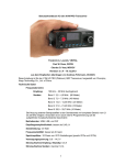
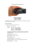
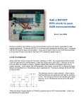
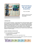
Build this Direct Digital Synthesizer "Development Kit"
By: Diz Gentzow, W8DIZ
A great tutorial for adding a keypad to the DDS Kit by Bruce, W8BH
This manual has been prepared to be read directly on screen. (Use CTRL+L on
Acroread or similar command in other PDF readers for “full-screen”). If you want to
print it, please use “Multiple page” option to save resources. Thank you.
General Notes:
The DDS Development Kit is fully functional as a Sig_Gen/VFO (once built).
the internal firmware currently displays:
line1: "DDS Dev Kit V2.0" - (Your callsign can be custom programmed upon
request)
line2: "nn,nnn.nnn Hz " - (where nn,nnn.nnn is the Frequency)
Programmed Frequency range is 1 Hz up to 29,999 kHz
Operates from 12 VDC at about 110 milliamps
Two channels RF output (control line selectable)
70-20 milliwatts output into a 50 Ω load from 1,800 KHz to 29,999 kHz,
respectively.
Freq range can be changed in firmware.
This DDS kit was designed to be a VFO source for NE602A and/or Diode Ring
mixers
Fully expandable using 20 CPU I/O lines to control other transceiver function.
Open Source code available under the GNU General Public License.
Quick user manual:
Supply power to the DDS using 12-14 VDC at 120 milliamps current draw.
On power-up, the Red LED blinks twice and then the LCD displays 10,000,000 Hz
Note there is a cursor under the 1 MHz position on the LCD.
Press the encoder and the cursor moves to the 100 KHz position.
Each press of the encoder will move the cursor to the right.
Pressing the encoder when the cursor is at the 1 Hz position causes the cursor to
move to the 10 MHz position.
Default Freq is 10 MHz; software programmable. IF OFFSET, both +/-, and band
selection via pre-programmed memories will be available soon.
100 MHz CLOCK calibration is available through a special program:
http://w8diz.com/qq-fc-project/9834/calc-9834.php
Building Instructions:
1. Inventory all Parts
The Kit includes two plastic parts bags; one with all the resistors; the other with the
remaining parts.
The parts bags may contain extra resistors and capacitors that are not used.
1 - PCB manufactured by http://expresspcb.com
Resistors (1/4 W)
1 - 10 Ω
R4
1 - 51 Ω
R22
1 - 120 Ω
R11
Brown
Green
Brown
- Black
- Brown
- Red
- Black - Gold
- Black - Gold
- Brown - Gold
Resistors (1/8 W)
1 - 3.3 Ω
R21
2 - 22 Ω
R33,34
1 - 51 Ω
R20
2 - 75 Ω
R31,32
5 - 100 Ω
R2,13,14,29,30
1 - 330 Ω
R18
Orange
Red
Green
Violet
Brown
Orange
-
-
Orange
Red
Brown
Green
Black
Orange
Gold
Black
Black
Black
Brown
Gold
-
Gold
Gold
Gold
Gold
Gold
Gold
Resistors (1/8 W) (cont.)
2 - 620 Ω
R6,35
Blue 4 - 1 kΩ
R3,19,27,28
Brown 1 - 2.7 kΩ
R12
Red
3 - 4.7 kΩ
R15,16,17
Yellow 10 - 10 kΩ
R1,5,7,8,9,10,23,24,25,26
Brown -
Red
Black
Violet
Violet
-
Brown
Red
Red
Red
Black
- Orange - Gold
Capacitors
1 - 22 pF
C3
1 - 30pF or 40pF - C2 trimmer (green or yellow, respectively)
2 - 100 pF
C20,22
1 - 220 pF
C21
5 - 10 nF
C10,11,12,27,28
7 - 47 nF
C15,18,23,24,25,29,30
9 - 100 nF
C1,4,5,6,7,14,16,17,26
1 - 330 nF
C13
2 - 47μF
C8,9 Electrolytic
1 - jumper
C19 (instead of a capacitor)
-
Gold
Gold
Gold
Gold
Crystal and oscillator
1 - 20.48 MHz crystal
1 - 100 MHz oscillator
X1
X2
Semiconductors
1 - ATmega88PA-20
1 - 74HC164
1 - 7805
1 - 78L33
1 - AD9834CRUZ
1 - 2N5109 transistor
2 - 2N3904 transistor
1 - red LED
2 - MPN3700 PIN diode
U1
U2
U3
U4
U5
Q1
Q2,3
D1
D2,3
Ferrites
1 - BN-43-2402
L1 inductor/filter 4 turns
1 - BN-61-2402
T1 transformer 6 turn : 3 turn
1 - FT37-43
T2 transformer 8+8 turn (bifilar)
2 - T30-6
L2,3 filter cores 8 turn
16 inches of 26 gage magnet wire
16 inches of 30 gauge magnet wire (dual twisted wires)
Miscellaneous
1 - Rotary Encoder
1 - RESET pushbutton
3 - 14 pin socket
1 - 2x3 Program Header
3 - 3-pin power header
1 - 16-pin LCD socket
1 - 16-pin LCD header
E1
S1
J1
J2,3,4
USER SUPPLIED PARTS:
three (3) feet of hookup wire
3-pin female connector for power input connection
3-pin female connector for receive RF output connection
3-pin female connector for transmit RF output connection
2. Install all 1/4 Watt Resistors.
Note: Bend the resistor leads a sharp 90 degrees from the body
____R4: 10 Ω
Brown - Black - Black - Gold
____R11: 120 Ω Brown - Red
- Brown - Gold
____R22: 51 Ω
Green - Brown - Black - Gold
3. Install all 1/8 Watt Resistors.
Note: Bend the resistor leads a sharp 90 degrees from the body
____R1,5,7,8,9,10,23,24,25,26: 10 kΩ
Brown - Black - Orange
____R2,13,14: 100 Ω
Brown - Black - Brown
____R3,19,27,28: 1 kΩ (1K0)
Brown - Black - Red
____R6,35: 620 Ω
Blue - Red
- Brown
____R12: 2.7 kΩ (2K7)
Red
- Violet - Red
____R15,16,17: 4.7 kΩ (4K7)
Yellow - Violet - Red
____R18: 330 Ω
Orange - Orange - Brown
____R20: 51 Ω
Green - Brown - Black
____R21: 3.3 Ω (3R3)
Orange - Orange - Gold
-
Gold
Gold
Gold
Gold
Gold
Gold
Gold
Gold
Gold
Note: If the DDS Receive output drives a +7dBM Diode Ring Mixer then place a
jumper wire at R31 else
if the DDS Receive output drives a 602 Gilbert Cell Mixer then install resistors
R29,31,33 else
design your own Receive output level resistor pad.
____R29: 100 Ω
Brown - Black - Brown - Gold
____R31: 75 Ω
Violet - Green - Black - Gold
____R33: 22 Ω
Red
- Red
- Black - Gold
Note: If the DDS Transmit output drives a +7dBM Diode Ring Mixer then place a
jumper wire at R32 else
if the DDS Transmit output drives a 602 Gilbert Cell Mixer then install resistors
R30,32,34 else
design your own Transmit output level resistor pad.
____R30: 100 Ω
Brown - Black - Brown - Gold
____R32: 75 Ω
Violet - Green - Black - Gold
____R34: 22 Ω
Red
- Red
- Black - Gold
4. Install three 14 pin DIP sockets.
____Position the socket notches at PIN-1/14 and solder.
5. Install the 20.48 MHz Crystal about 1/32 inch above the PCB.
____Insert the Crystal in the PCB and tilt it; hold with one finger and solder.
Straighten the XTAL.
6. Install the following capacitors on the digital side (right side) of the PCB.
____C1,4,5,6,7: 100n yellow axial lead bypass capacitors
____C2: 40p yellow trimmer capacitor; FLAT SIDE toward C1 (picture shows a
green trimmer)
____C3: 22p NPO axial lead capacitor
7. Install type 43 ferrite binocular below C5.
There are two binoculars in the parts kit; one has rounded corners and is shiny
black, the other has sharp corners and is dull black.
The shiny, rounded corners ferrite binocular is a type -43; the other is a type -61.
Cut 4 inches of 30 GA green wire and insert 4 complete turns through the -43
binocular.
One turn is defined are a wire running through BOTH HOLES of the binocular.
Strip the insulation off the wires all the way down to the body of the binocular core.
Tin the wires.
____L1: Insert the BN-43-2402 binocular filter inductor (standing up) and solder.
8. Install Red LED at .
____D1: Red LED; note polarity (flat side) and solder.
9. Install electrolytic capacitors.
____C8,9: 47uF; note polarity (+) and solder.
10. Install 4 pin reset push putton; note polaririty; only fints one way into the PCB
____RESET: Insert and solder.
11. Install the 6 pin programming header to the left of C8
____Solder.
12. Install the 3 terminal voltage regulator in lower right corner of the PCB (not
labeled).
____U3: LM7805AC; note polarity; Metal TAB toward C8; solder.
13. Install the 16-PIN female LCD header on the left side of the PCB
Before installing the female LCD header, you might want to consider how and
where you want the LCD to display.
You may want to make an extension cable by soldering 16 wires between the PCB
and the female header.
____Install and solder both male and female, header and socket.
14. Connect a 3-PIN header at J2 or connect power wires to J2; center pin is +12V
(wires are not supplied)
____+12V + GND wires: solder.
15. Apply 12Vdc power to J2
____Measure 5 volts across C7; if not 5V then fix the problem before proceeding.
16. Install the surface mount DDS chip (optionally installed by kitsandparts)
*** Please be carefull installing the AD9834 ***
Align the chip on the SMT pad, PIN-1 toward R12. Tack solder one corner of the
DDS chip.
Solder the remaining pins to the SMT pad. Use solder wick to remove solder
shorts.
Review soldering mess using high power magnifying glass, optionally check for
shorts using ohm meter.
____AD9834CRUZ
17. Install type 61 ferrite binocular above R12.
There are two binoculars in the parts kit; one has rounded corners and is shiny
black, the other has sharp corners and is dull black.
The shiny, rounded corners ferrite binocular is a type -43; the other is a type -61.
Cut 8 inches of 30 GA red wire and insert 6 complete turns through the -61
binocular.
The binocular holes are small so make sure the turns are tight to allow additional
winding to be added.
One turn is defined as one wire running through BOTH HOLES of the binocular in
a U patern.
Cut 4 inches of 30 GA green wire and insert 3 complete turns through the -61
binocular.
The completed transformer should have 2 red wires coming out one end of the
binocular and 2 green wires on the other end.
Strip the insulation off the wires all the way down to the body of the binocular core.
Tin the wires.
____L1: Insert the BN-61-2402 binocular transformer (red wires toward R13), pull
leads tight and solder.
18. Install the following capacitors on the DDS side (left side) of the PCB.
Note that C15 is labeled twice (in error) on the PCB. C15 in the next step is
between C14 and C16.
____C15,18,23,24,25,29,30: 47n yellow axial lead capacitors
____Install a jumper (discarded resistor lead) at location labeled C15 between R13
and R14
____C14,16,17,26: 100n yellow axial lead capacitors
____C10,11,12,27,28: 10n yellow radial lead disk capacitors
19. Install T2, a bifilar wound transformer.
Prepare 8 inches of 30 GA dual red/green magnet wire. Twist tightly to about 4
twists per inch.
Wind 8 turns, evenly and tight through the body of the FT37-43 ferrite toroid.
Trim leads to about half inch from the toroid body. Remove insulation up to the
body of the ferrite.
It is required that one colored wire is installed in the upper right corner connected
to C25 and the other colored wire is connected in the lower left corner connected
to the collector of Q1.
The remaining red and green wires run through the holes connecting to R19 and
the PIN diodes.
____FT37-43 Strip and Tin leads; and install.
20. Install two T30-6 yellow toroid inductors (low pass filter cores).
Prepare 2 pieces of 7 inches of 26 GA red magnet wire.
Wind 8 turns of the wire through one yellow toroid. Repeat for the
other toroid.
Strip the insulation off the wires all the way down to the body of the
toroid cores.
Tin the wires.
____L2,3: Install the T37-6 toroids (standing up) and solder.
21. Install large yellow capacitor and 3.3 volt regulator
____C13: 330n yellow radial lead capacitor
____U4: 78L33 - 3 terminal voltage regulator; observe polarity
22. Install low pass filter capacitors
____C20,22: 100p
____C21: 220p
23. Install semiconductors
____Q1: 2N5109 - install about 1/16 inch or 2 mm above the PCB.
____Q2,3: 2N3904 - install with about 1/4 inch or 6 mm leads above the PCB.
Observe polarity and do not overheat.
____D2,3: MPN3700 - install the PIN diodes all the way against the PCB. Observe
polarity and do not overheat.
24. Install the 100 MHz Clock
____X2: 100 MHz - observe polarity; Squared corner points toward the lower left
corner of the PCB
25. Install the Rotary Mechanical Encoder, a pulled part recycled from a Panasonic
AM/FM Auto Radio.
____E1: Solder
26. Install the power connection jumpers between the DDS and CPU sections of
the PCB
The following step installs jumpers but could be replaced with inductors to possibly
reduce circuit noise.
____VCC: Install a jumper at VCC located in the center of the PCB and to the left
of the trimmer capacitor.
____GND: Install a jumper at GND located at the lower left of the 20.48 crystal.
27. Connect the DDS section to the CPU section (a total of six (6) wire jumpers)
These connections are firmware dependent. Current firmware requires the
following connections:
____PD4: Connect PD4 from the Encoder to PD4 on the ATmel CPU.
____PD2: Connect PD2 from the Encoder to PD2 on the ATmel CPU.
____PD3: Connect PD3 from the Encoder to PD3 on the ATmel CPU.
____PD5: Connect SD from the AD9834 to PD5 on the ATmel CPU.
____PD1: Connect SC from the AD9834 to PD1 on the ATmel CPU.
____PD0: Connect FS from the AD9834 to PD0 on the ATmel CPU.
28. Install the ICs; before inserting the ICs into their sockets, bend the IC pins so
that they are at sharp right angles to the IC`s plastic body. The easiest way to
bend all leads uniformly is to place the IC legs on a flat table and push/press the
body of the IC against the table. DO both sides.
____U1: ATmega88PA-20 - install observing PIN-1 polarity
____U2:74HC164 - install observing PIN-1 polarity
29. Connect the LCD to the PCB.
____OK
30. Momentarily connect 12 volt power to the PCB, observing current draw (if
possible)
Current consumption should be about 120 milliamps.
When the DDS powes up, the LED should flash twice and then the LCD should
display 10,000,000 Hz.
If all is OK at this point, connect 12 volts to either the TRANSMIT or RECEIVE
control lines and measure/view 10 MHz output from the corresponding TRANSMIT
or RECEIVE outputs at J3/4.
Output level into a 50 ohm dummy load should be about 4.8 volts Peak-to-Peak at
10 MHz, provided that there is no resistor pad in the output section on the PCB.
____OK
31. Assuming that all is OK to this point, the next step is to set up the DDS as a
development platform. This step is optional; not required if you plan to use the
DDS Kit as a Sig_Gen or VFO.
Click on the Development Platform Link for information to update and/or modify the
firmware.