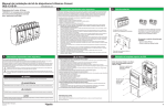
1
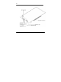
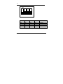
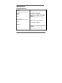
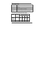
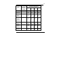
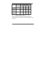
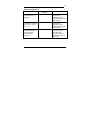
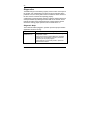
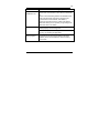
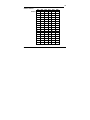
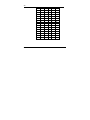
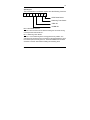
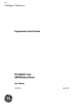
PCI Genius® Card
Quick Install Guide
PCI Genius Card
IC660ELB931
October 2004
________________________________________
GFK-2342
GFL-002
Warnings, Cautions, and Notes as Used in this Publication
Warning
Warning notices are used in this publication to emphasize that hazardous voltages,
currents, temperatures, or other conditions that could cause personal injury exist in
this equipment or may be associated with its use. In situations where inattention
could cause either personal injury or damage to equipment, a Warning notice is used.
Caution
Caution notices are used where equipment might be damaged if care is not taken.
Note:
Notes merely call attention to information that is especially significant to
understanding and operating the equipment.
This document is based on information available at the time of its publication. While efforts
have been made to be accurate, the information contained herein does not purport to cover
all details or variations in hardware or software, nor to provide for every possible contingency
in connection with installation, operation, or maintenance. Features may be described herein
that are not present in all hardware and software systems. GE Fanuc Automation assumes
no obligation of notice to holders of this document with respect to changes subsequently
made.
GE Fanuc Automation makes no representation or warranty, expressed, implied, or statutory
with respect to, and assumes no responsibility for the accuracy, completeness, sufficiency,
or usefulness of the information contained herein. No warranties of merchantability or fitness
for purpose shall apply.
Any trademarks referenced herein are used solely for purposes of identifying compatibility
with the products of GE Fanuc Automation.
©Copyright 2004 GE Fanuc Automation North America, Inc.
All Rights Reserved.
The PCI Genius Card has been tested and found to meet or exceed the requirements of U.S.
(47 CFR 15), Canadian (ICES-003), Australian (AS/NZS 3548) and European (EN55022)
regulations for Class A digital devices when installed in accordance with guidelines noted in
this manual.
Note: This device complies with Part 15 of the FCC rules. Operation is subject to the
following two conditions: (1) This device may not cause harmful interference, and
(2) This device must accept any interference received including interference that
may cause undesired operation.
Note: This Class A digital apparatus complies with Canadian ICES-003.
Note: This equipment has been tested and found to comply with the limits for a Class A
digital device, pursuant to Part 15 of the FCC Rules. These limits are designed to
provide reasonable protection against harmful interference when the equipment is
operated in a commercial environment. This equipment generates, uses, and can
radiate radio frequency energy and, if not installed and used in accordance with the
instruction manual, may cause harmful interference to radio communications.
Operation of this equipment in a residential area is likely to cause harmful
interference in which case the user will be required to correct the interference at his
own expense.
Note:
Any changes or modifications to the product or installation that are not expressly
approved by GE Fanuc Automation could void the user's authority to operate the
equipment under FCC rules.
The following statements are required to appear for Class 1, Div 2 Hazardous Locations.
1. EQUIPMENT LABELED WITH REFERENCE TO CLASS 1, GROUPS A, B, C, AND D,
DIV 2 HAZARDOUS LOCATIONS IS SUITABLE FOR USE IN CLASS 1, DIVISION 2,
GROUPS A, B, C, D, OR NON-HAZARDOUS LOCATIONS ONLY.
2. WARNING - EXPLOSION HAZARD - SUBSTITUTION OF COMPONENTS MAY IMPAIR
SUITABILITY FOR CLASS 1, DIVISION 2.
3. WARNING - EXPLOSION HAZARD - DO NOT DISCONNECT EQUIPMENT UNLESS
POWER HAS BEEN SWITCHED OFF OR THE AREA IS KNOWN TO BE
NONHAZARDOUS.
4. WARNING - EXPLOSION HAZARD - WHEN IN HAZARDOUS LOCATIONS, TURN OFF
POWER BEFORE REPLACING OR WIRING MODULES
Table of Contents
Table of Contents.................................................................. 5
Description ............................................................................ 7
PCI Genius Card ...........................................................................7
Faceplate ......................................................................................7
Software ........................................................................................8
Programming Interface..................................................................8
Installing the PCI Genius Card ............................................ 9
Mechanical Overview............................................................ 9
Indicators ............................................................................. 11
Connecting the Bus ............................................................ 13
Sample Bus Configuration ................................................. 13
DIP Switch Setting .............................................................. 15
Bus Termination Resistor Setting................................................15
Specifications...................................................................... 17
Board Specifications....................................................................17
Network Specification..................................................................18
Bus Cable Type and Maximum Cable Length: ............................18
Product Certification ....................................................................21
Diagnostics .......................................................................... 22
Diagnostic Steps .........................................................................22
Appendix A .......................................................................... 25
History .........................................................................................25
PCI Genius Card
GFK-2342
PCI Configuration........................................................................26
Functional Registers....................................................................27
Shared RAM Memory Map..........................................................35
PCI Genius Card
GFK-2342
7
Description
PCI Genius Card
The PCI Genius card provides an intelligent interface between a PCI
slot in a PC compatible computer and a single channel general purpose
controller interface to the Genius serial bus. This card complies with
Rev 2.2 of PCI Local Bus Specification and handles all the interface and
protocol tasks associated with the Genius bus communications. The
primary function of this card is to provide a means for third parties to
interface the CPU, PLC, or Genius I/O Blocks on the Genius bus.
Faceplate
The PCI Genius card has a 4-pin right angle male terminal box
connector with retention screws for the Genius I/O interface. Two LEDs
(GENI OK and COMM OK) on the faceplate indicate the single channel
Genius bus status. Openings in the faceplate accommodate the bus
connector and LEDs.
PCI Genius Card
GFK-2342
8
Software
If you are using the PCI Genius card with Machine Edition software,
Machine Edition installs custom drivers for its use. Please consult the
topic "Installing the device driver for a PCI device (card)" in the Machine
Edition online help for more details.
If you are not using Machine Edition, you can use a Windows driver for
the PCI Genius card that is available for Windows NT4, 2000, and XP.
This driver allows user-mode programs to gain access to the PCI
Genius card’s Shared RAM, configuration register, status register, and
control register and also to determine the physical bus and slot of the
card. The driver is available under special license from GE Fanuc.
Contact the GE Fanuc Global Customer Care Center at
1-800-GEFANUC for more details concerning part number
44A750896-G01.
Programming Interface
Programming user applications to communicate with the drivers are not
covered in this manual. Users wishing to write their own interface to the
hardware should see Appendix A for hardware register details.
PCI Genius Card
GFK-2342
9
Installing the PCI Genius Card
Warning:
Always use anti-static precautions when handling
the PCI Genius card or working inside the host
computer.
1. Power off the host computer and unplug it from its power source.
2. Install the PCI Genius card according to computer manufacturer's
instructions for option cards.
3. Power up the computer and login to Windows.
Mechanical Overview
The PCI Genius card is shown on the next page. The interface card will
plug into PCI slot of a computer. The Genius bus connector is where the
Genius bus cable is connected to the module. DIP switches are used to
set the termination resistance for the Genius bus. LED indicators display
the status of the module.
PCI Genius Card
GFK-2342
10
PCI Genius Card
GFK-2342
11
Indicators
The Genius Interface module has two LED indicators on the faceplate.
These are used for displaying the status of the module.
PCI Genius Card
GFK-2342
12
LED
Communication
OK
Genius OK
PCI Genius Card
LED
Status
Description
ON
The Genius Interface can send and receive
data on the serial bus.
OFF
(Flashing)
An error has been detected in communications
on the serial bus.
ON
Power is available to the Genius Interface, and
the onboard self-diagnostics passed.
OFF
The watchdog timer has timed out, indicating a
board failure.
GFK-2342
13
Connecting the Bus
Devices can be connected in any physical sequence on the bus.
The Genius bus connector has four terminals for the bus cable:
(Serial 1 (X1), Serial 2 (X2), Shield In (SI), and Shield Out (SO)).
Connect the Serial 1 terminal of each connector to the Serial 1
terminals of the previous device and the next device. Connect the
Serial 2 terminal of each connector to the Serial 2 terminals of the
previous device and the next device. Shield In of each connector
must be connected to Shield Out of the preceding device. For the
first device on the bus, Shield In can be left unconnected. For the
last device on the bus, Shield Out can be left unconnected.
Sample Bus Configuration
Terminating
Resistor
Start
of Bus
PCI Genius Card
End
of Bus
Terminating
Resistor
GFK-2342
14
Caution: When making bus connections, the maximum exposed
length of bare wires should be two inches. For added
protection, each shield drain wire should be insulated with
electrically isolated tubing to prevent the Shield In and
Shield Out wires from touching each other.
Refer to The Genius I/O System and Communications User’s
Manual, GEK-90486-1 for additional details on Genius bus wiring.
PCI Genius Card
GFK-2342
15
DIP Switch Setting
Bus Termination Resistor Setting
A bus must be terminated at each end by the correct impedance for the
particular cable type. The impedance will be either 75, 100, 120, or 150
ohms. Install the appropriate terminating resistor across the Serial 1 and
Serial 2 terminals.
The Genius Interface has on-board termination resistors that can be
selected by the DIP switch setting. The Genius I/O System and
Communications User’s Manual, GEK-90486-1 lists appropriate
terminating resistors for each recommended bus cable type.
The DIP switch configuration should be set according to the description
on the next page.
PCI Genius Card
GFK-2342
16
ON
1
2
3
4
Pole1
Pole 2
Pole3
Pole 4
Resistor Value
ON
OFF
OFF
OFF
150 OHM
ON
ON
OFF
OFF
125 OHM
100 OHM
ON
ON
ON
OFF
ON
ON
ON
ON
75 OHM
OFF
OFF
OFF
OFF
*NONE
* Default setting.
PCI Genius Card
GFK-2342
17
Specifications
Board Specifications
Environmental:
Operating:
Operating temperature at board
Humidity
Vibration
Shock
Non–operating:
Ambient Temperature at board
Humidity
Vibration
Shock
PCI Genius Card
0°C to +60°C, 32°F to + 140°F
5% to 95% non–condensing
IEC 68-2-6; 10 - 57Hz, 0.012" peak to peak
displacement; 57 - 500Hz, 1.0g constant
acceleration.
IEC 68-2-27; 15g, 11ms (sine wave).
–40°C to +85°C, –40°F to +185°F
5% to 95% non–condensing
IEC 68-2-6; 10 - 57Hz, 0.012" peak to peak
displacement; 57 - 500Hz, 1.0g constant
acceleration
IEC 68-2-27; 15g, 11ms (sine wave).
GFK-2342
18
Network Specification
Bus Type
Daisy-chained bus cable; single twisted pair plus shield or
Twinax
Bus Termination
On board DIP switch selectable: None, 75, 100, 120, or
150 ohms.
Baud Rate
Configurable 153.6 Kbaud standard, 153.6 Kbaud
extended, 76.8 Kbaud, or 38.4 Kbaud.
Max. Number of
Devices
32 devices at 153.6 Kbaud standard, 153.6 Kbaud
extended, or 76.8 Kbaud. 16 devices at 38.4 Kbaud.
Bus Cable Type and Maximum Cable Length:
Cable #
& Make
Terminating
Resistor
–10%to+20%
1/2 Watt
Maximum Length Cable Run,
feet/meters at baud rate
153.6s
153.6e
76.8
38.4 •
(A)9823
(B)9182
(C)4596
(M)M39240
150 ohms
2000ft
606m
3500ft
1061m
4500ft
1364m
7500ft
2283m
(B)89182
150 ohms
2000ft
3500ft
4500ft
7500ft
PCI Genius Card
GFK-2342
19
Cable #
& Make
Terminating
Resistor
–10%to+20%
1/2 Watt
Maximum Length Cable Run,
feet/meters at baud rate
153.6s
153.6e
76.8
38.4 •
606m
1061m
1364m
2283m
(B)9841
(M)M3993
120 ohms
1000ft
303m
1500ft
455m
2500ft
758m
3500ft
1061m
(A)9818C
(B)9207
(M)M4270
100 ohms
1500ft
1818m
2500ft
455m
3500ft
758m
6000ft
1061m
(A)9109
(B)89207
(C)4798
(M)M44270
100 ohms
1500ft
1818m
2500ft
455m
3500ft
758m
6000ft
1061m
(A)9818D
(B)9815
100 ohms
1500ft
1818m
2500ft
455m
3500ft
758m
6000ft
1061m
(A)9818
(B)9855
(M)M4230
100 ohms
1200ft
364m
1700ft
516m
3000ft
909m
4500ft
1364m
(A)9110
(B)89696
100 ohms
1200ft
364m
1700ft
516m
3000ft
909m
4500ft
1364m
PCI Genius Card
GFK-2342
20
Cable #
& Make
Terminating
Resistor
–10%to+20%
1/2 Watt
Maximum Length Cable Run,
feet/meters at baud rate
153.6s
153.6e
76.8
38.4 •
(B)89855
(M)M64230
(A)9814C)
(B)9463
(M)M4154
75 ohms
800ft
242m
1500ft
455m
2500ft
758m
3500ft
1061m
(A)5902C
(B)9302
(M)M17002
75 ohms
800ft
242m
1500ft
455m
2500ft
758m
3500ft
1061m
Notes:
A = Alpha, B = Belden, C = Consolidated, M = Manhattan
• = Limited to 16 taps at 38.4 Kbaud
Refer to The Genius I/O System and Communications User’s
Manual, GEK-90486-1 for details on selection and installation of the
bus cable.
PCI Genius Card
GFK-2342
21
Product Certification
Description
Agency Standard or
Marking
Comments
North American Safety
for Industrial Control
Equipment
UL 508/C-UL
Certification by
Underwriter’s
Laboratories to UL
standard and equivalent
CSA standard
North American Safety
for Hazardous Locations
Class I, Div. 2, Groups
A, B, C, D
UL 1604C-UL
Certification by
Underwriter’s
Laboratories to UL
standard and equivalent
CSA standard
Electromagnetic
Compatibility Directive
European EMC for
Industrial Control
Equipment
CE
Certification by
Competent Body in
accordance with
European Directives.
Refer to Declaration of
Conformity.
PCI Genius Card
GFK-2342
22
Diagnostics
Troubleshooting involves thinking logically of the function of each part of
the system, and understanding how these functions interrelate. When
problems occur, the total system must be considered. All the devices on
the bus must be connected and operating properly.
A malfunction causing improper operation of Genius Interface board can
usually be isolated by checking the board LEDs on the module. These
indicate the status of the board itself and its communications with the
Genius bus. During proper operation, both the LEDs will be on.
Diagnostic Steps
The module should be plugged in, powered up and the proper software
application should be running:
Indication
Genius OK is off
COMM OK is on
PCI Genius Card
Troubleshooting Steps
Make sure the correct parameters are entered using the
configuration software.
Ensure that the Genius interface Module is completely
inserted in the host backplane connector, and that all
connector pins are properly aligned.
If these steps do not correct the problem, replace the
Genius Interface Module.
GFK-2342
23
Indication
Troubleshooting Steps
Genius OK is on
COMM OK is off
Ensure correct cable type and length (see Genius I/O
System and communications User’s Manual, GEK-904861).
Ensure correct terminating resistors are installed at both
ends of the bus length (see Genius I/O System and
communications User’s Manual, GEK-90486-1).
Ensure the serial bus is wired in a daisy-chain fashion.
Make sure cabling is not in proximity to high voltage runs.
Make sure cable is not broken.
Both LEDs are off
Make sure the Genius interface Module is plugged in,
seated properly, and receiving power.
Make sure the proper software application is loaded and
running. (Try reloading the application)
Both LEDS are
flashing together
PCI Genius Card
Two devices on the same bus have probably been
configured with the same Device Number (serial bus
address). Check the bus addresses, and if necessary
correct them.
GFK-2342
24
Indication
Troubleshooting Steps
Repeated bus
errors occur
Ensure that cable shielding is properly installed and
Grounded (see Genius I/O System and communications
User’s Manual, GEK-90486-1).
Unplug the bus communications cable from the Interface
Module, verify the serial bus addresses (SBAs) of all
network nodes with a hand-held monitor (HHM), and use
the HHM to read the configuration and verify device
numbers and I/O reference numbers.
Bus errors--can’t
get the Interface
Module up and
running
Serial 1 and Serial 2 are crossed.
Correct the bus wiring (see “Sample Bus Configuration”
on page 14.)
Intermittent or total
lack of
communications
Mixed baud rates.
Power up blocks one at a time and confirm the baud rate
for each. Any changes to baud rate in a block will not take
effect until block power is cycled.
PCI Genius Card
GFK-2342
25
Appendix A
Many users of the ISA bus Genius cards have developed private
software that interfaces with the Genius network. This appendix
provides hardware details to help those users transition to the PCI card.
History
In working with the GENIUS PCI card, it is helpful to understand some
of the history of the GENIUS PC interfaces. The core of the GENIUS PC
interface products is a shared memory module called a GENI or µGENI,
which is described in the Genius I/O µGENI Board User’s Manual,
GFK-0845. This module has a 16Kbyte memory mapped interface that
allows a host processor to communicate on the GENIUS network. The
other input and output signals to a µGENI module are the four GENIUS
bus lines, two LED signals, and eight initialization signals that specify
the card's SBA, network baud rate, and output enabled status.
Previous ISA PC GENIUS cards either implemented the µGENI circuitry
as a single circuit board or had a carrier ISA circuit board that allowed
one or two µGENI daughter modules to attach to the carrier ISA circuit
board. The eight initialization signal values and the address information
as to where the µGENI mapped into the ISA space were programmed
into non-volatile memory on the carrier board. This configuration
information resided at one range of I/O registers and control of the reset
PCI Genius Card
GFK-2342
26
and watchdog lines going into the µGENI hardware were controlled at a
second set of I/O registers.
The GENIUS PCI card continues this tradition. The µGENI module has
been integrated onto the single circuit board and the setup signals and
control of the reset and watchdog functions have been mapped to I/O
registers. There is no non-volatile memory on the PCI card, so the card
does not retain its SBA address, bus baud rate, or output enable state in
non-volatile storage.
PCI Configuration
The Device and Vendor IDs of the PCI Genius card are 0x0100 and
0x1FC3. The card reports five resource descriptors:
-
An interrupt descriptor
-
A four byte I/O area for the Functional Registers
A memory and I/O region of length 128 bytes for access to the
internal PCI hardware
A 16K byte memory area for the Shared RAM
Users programming their own drivers should only need to access the
Functional Registers and Shared RAM in most cases.
PCI Genius Card
GFK-2342
27
Functional Registers
The PCI Genius card has three I/O mapped registers. The PCI stack
maps these registers into I/O space The Windows driver controls
access to these registers.
Register
Size
Description
Access Type
0
1 Byte
Configuration Register
Read /Write
1
1 Byte
Status Register
Read only
2
1 Byte
Control Register
Read /Write
PCI Genius Card
GFK-2342
28
Configuration Register
The Configuration register must be programmed prior to releasing the
PCI Genius card from reset. The bits of this register are read by the
µGENI firmware during its initialization. The bits of this register are
described below:
Bit
Name
Function
7
Output
Enable
0=enabled
1=disabled (Default)
6—5
Baud Rate
Serial Bus Baud Rate
00=153.6 Kbaud Extended (8 bit skip time)
01=38.4 Kbaud (8 bit skip time)
10=76.8 Kbaud (8 bit skip time)
11=153.6 Kbaud Standard (4 bit skip time) (Default)
4—0
Address
Serial Bus Address, see “Serial Bus Addresses” on
page 29.
PCI Genius Card
GFK-2342
29
Serial Bus Addresses
Default
PCI Genius Card
Bit4
Bit3
Bit2
Bit1
Bit0
SBA
0
0
0
0
0
0
0
0
0
0
1
1
0
0
0
1
0
2
0
0
0
1
1
3
0
0
1
0
0
4
0
0
1
0
1
5
0
0
1
1
0
6
0
0
1
1
1
7
0
1
0
0
0
8
0
1
0
0
1
9
0
1
0
1
0
10
0
1
0
1
1
11
0
1
1
0
0
12
0
1
1
0
1
13
0
1
1
1
0
14
0
1
1
1
1
15
1
0
0
0
0
16
GFK-2342
30
PCI Genius Card
Bit4
Bit3
Bit2
Bit1
Bit0
SBA
1
0
0
0
1
17
1
0
0
1
0
18
1
0
0
1
1
19
1
0
1
0
0
20
1
0
1
0
1
21
1
0
1
1
0
22
1
0
1
1
1
23
1
1
0
0
0
24
1
1
0
0
1
25
1
1
0
1
0
26
1
1
0
1
1
27
1
1
1
0
0
28
1
1
1
0
1
29
1
1
1
1
0
30
1
1
1
1
1
31
GFK-2342
31
Status Register
The individual bits in the Status register have the following functions:
7
6
5
4
3
2
1
0
GENI Reset Detect
Watchdog Timer Status
GENI OK
COMM OK
Bit 0 –GENI RESET Detect
This bit is set to 0 whenever PCI Genius board goes into reset. During
normal operation this bit will be 1.
Bit 1 – Watchdog Timer Status
This bit is 1 if the watchdog timer is being pulsed every 500ms. The
watchdog timer is pulsed by the accesses into the Shared Memory area.
If the timer expires, this bit goes to 0. The Shared RAM area should be
accesses to set this value before enabling the watchdog timer.
PCI Genius Card
GFK-2342
32
Bit 3 –GENI OK
The state of this bit follows the condition of the GENI OK LED on the
board. If the LED is lit, the GENI OK bit is 0. This bit also indicates the
MIT watchdog timer (an onboard firmware watchdog timer) has timed
out, indicating a failure in the onboard firmware. The board can be reset
by pulsing bit 6 of the control register to low and then high again.
Bit 4 – COMM (Communications) OK
Like the GENI OK bit, this bit follows the output of one of the LED’s on
the board. This bit is 0 if the COMM OK LED on the board is lit.
PCI Genius Card
GFK-2342
33
Control Register
The individual bits in the Control register are used for the following
functions:
7
6
5
4
3
2
1
0
HHM Present Test
WDT Enable
Board Reset
Bit 3 – HHM Test
An HHM present can be indicated even when one is not plugged in by
raising this bit to 1. After power up and under normal conditions, this bit
should be 0. It is not used on the PCI Genius card.
Bit 5 – WDT Enable
When this bit is 0 it enables the hardware watchdog timer. The host can
set this bit to '1' to disable the watchdog timer. During power on this bit
will be default zero (watchdog timer enabled).
Bit 6 –Board RESET
When this bit is 0 it resets the PCI Genius board. Under normal running
conditions, it should be 1. During power on, this bit will default to 0.
Before setting this bit to 1, the host can update the configuration register
PCI Genius Card
GFK-2342
34
and the control register; this bit can be set to 1 to bring the board out of
reset.
Watchdog Timer
The watchdog timer provides watchdog time out period of 0.99 seconds.
Once the watchdog circuit is enabled, it will monitor access to the
Shared RAM area of the card. If the host does not access the card
within the 0.99 seconds +/- 25% the watchdog expires. It is
recommended that host application should communicate with the
Genius card at least once every 0.5 second. The host should access
the Shared RAM area at least one before enabling the watchdog to
reset the timeout before enabling the watchdog reset feature.
PCI Genius Card
GFK-2342
35
Shared RAM Memory Map
The 16Kbyte Shared RAM area is allocated by the PCI stack. User
applications must use a Windows driver to access this area or map it to
the process address space.
Host Address
Content
Base + 0x0000
Request Queue
Size in bytes
2176
Base + 0x0880
Request Queue Head Pointer
1
Base + 0x0881
Request Queue Tail Pointer
1
Base + 0x0882
Setup Table
16
Base + 0x0892
Status Table
16
Base + 0x08A2
Interrupt Status Table
16
Base + 0x08B2
Interrupt Disable Table
16
Base + 0x08C2
Command Block
16
Base + 0x08D2
Transmit Datagram Buffer
240
Base + 0x09C2
Read Datagram Buffer
134
Base + 0x0A48
I/O Table lockout Request
1
Base + 0x0A49
I/O Table lockout state
1
Base + 0x0A4A
Host Clear
1
Base + 0x0A4B
Reserved
64
PCI Genius Card
GFK-2342
36
Host Address
Content
Size in bytes
Base + 0x0A8B
Auxiliary Request Queue
48
Base + 0x0ABB
Heartbeat Enable
2
Base + 0x0ABD
Heartbeat Timeout Multiplier
1
Base + 0x0ABF
Reserved
4930
Base + 0x1E00
Device Configuration Table
256
Base + 0x1F00
Directed Control Input Table
128
Base + 0x1F80
Broadcast Control Output Table
128
Base + 0x2000-0x3FFF
Device I/O Table
8192
For more details on how to operate the Shared RAM Interface refer to
the Genius I/O µGENI Board User’s Manual, GFK-0845.
PCI Genius Card
GFK-2342