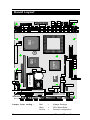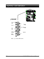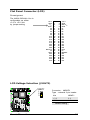
1
Copyright© 2000,2001 All Right Reserved. Manual Edition 1.2, March 2001 The information in this document is subject to change without prior notice in order to improve the reliability, design and function. It does not represent a commitment on the part of the manufacturer. Under no circumstances will the manufacturer be liable for any direct, indirect, special, incidental, or consequential damages arising from the use or inability to use the product or documentation, even if advised of the possibility of such damages. This document contains proprietary information protected by copyright. All rights are reversed. No part of this manual may be reproduced by any mechanical, electronic, or other means in any form without prior written permission of the manufacturer. Trademarks SIS is a trademark of Silicon Integrated System Crop.; DiskOnChip(r)2000 and TrueFFS are registered trademarks of M-Systems Inc.; IBM PC is a registered trademark of International Business Machines Corporation; Intel is a registered trademark of Intel Corporation; AMD is a registered trademark of Advanced Micro Devices, Inc.; AWARD is a registered trademark of Award Software international, Inc.. Other product names mentioned herein are used for identification purposes only and may be trademarks and/or registered trademarks of their respective companies. Part number :MPRT-UM Table of Contents Introduction ................................................................................... 1 Specifications ............................................................................... 2 Component Locations .................................................................. 6 Dimensions .................................................................................... 7 Board Layout ................................................................................ 8 Jumper / Connector Quick Reference ........................................ 9 CPU and CMOS Jumper Settings .............................................. 10 CPU Clock Speed (JR0~JR2, JF0~JF2) ............................................................. 10 CPU Voltage (JV0~JV4) ..................................................................................... 11 CMOS Operation (JRTC) ..................................................................................... 11 Watchdog Timer ......................................................................... 12 Mode Setting (JP4) ............................................................................................ 12 Time-out Setting (SWDT) ................................................................................... 12 Programming Example ....................................................................................... 13 DiskOnChip® 2000 Flash Disk .................................................... 14 Installation Instructions ...................................................................................... 14 Power Connectors ...................................................................... 15 Power Connector (PWRCON1) ......................................................................... 15 ATX Power Cotrol (PWRCON2) ......................................................................... 15 CPU / System Fan Connector (CPUFAN1 / SYSFAN1) ..................................... 15 Ethernet 10Base-T/100-Base-TX ................................................. 16 Disabling the Ethernet Controller ....................................................................... 17 LAN Port Signals ............................................................................................... 17 LAN LED Indicator (LED) ................................................................................... 17 Audio ESS Solo-1 ES-19385 ....................................................... 18 Disabling the Audio Controller ........................................................................... 19 Serial Port COM2 Mode (RS-232/485) ........................................ 19 COM RS-232C/485 Selection (J2) ..................................................................... 19 Switches and Indicators ............................................................. 20 Interface Connectors HDD, FDD ................................................. 21 Floppy Disk Drive (Floppy) ................................................................................ 21 EIDE Connector (Primary_IDE, Secondary_IDE) ............................................... 22 Peripheral Ports .......................................................................... 23 Parallel Port (Print) ............................................................................................. 23 USB Port (USB) ................................................................................................. 23 Onboard RS-232 Serial Port (JCOM1,2,3,4) .................................................... 24 RS-485 Serial Ports (RS1) ................................................................................ 24 IrDA (SIR) ........................................................................................................... 24 16-bit General Purpose I/O (JDIO) ..................................................................... 24 Flat Panel VGA (LCD1) ...................................................................................... 25 CRT SVGA (VGAH) ........................................................................................... 25 PS/2 Keyboard (PS2-KB) .................................................................................. 27 PS/2 Mouse (PS2-MS) ....................................................................................... 27 Audio Interface (JAUDIO) ................................................................................. 27 CDROM audio interface (MITSUMI) ................................................................... 27 System Resources ...................................................................... 27 SIS-530 AGP for CRT .................................................................. 29 Memory Assignment .......................................................................................... 29 C&T 69000 Flat Panel Controller ............................................... 30 Flat Panel Connector (LCD) ............................................................................... 30 LCD Voltage Selection (JVOLT1) ...................................................................... 30 PLANAR EL640.480-AA1 ................................................................................. 32 KYOCERA KCB104VG2BA-A01 ....................................................................... 33 SHARP LQ12S41 ............................................................................................... 34 HITACHI LMG9211XUCC .................................................................................... 35 NAN YA LTBSHT024GC ..................................................................................... 36 TORISAN MXS121022010 ................................................................................. 37 NEC NL8060AC26-04 ........................................................................................ 38 AWARD BIOS Setup .................................................................... 40 Standard CMOS Setup ....................................................................................... 41 BIOS Features Setup ......................................................................................... 44 Chipset Features Setup ..................................................................................... 47 Power Management Setup ................................................................................ 50 PNP/PCI Configuration ........................................................................................ 53 Hardware Monitor ............................................................................................. 55 Integrated Peripherals ......................................................................................... 56 Integrated Peripherals (NASA-582VLA version) ................................................. 56 POST Codes ................................................................................ 59 Audible Error Messages .................................................................................... 59 Visible Error Messages ..................................................................................... 59 POST Card Error Messages .............................................................................. 61 Howto : Flash the BIOS .............................................................. 66 Warranty ...................................................................................... 67 Introduction The NASA-582VLA is a 5.25" drive size single board computer that can drive both CRT and Flat Panel Displays. The board supports the latest high speed socket 7 CPUs. With its small form factor and high performance, the board is a cost/effective solution for demanding application such as GUI-based MMI solutions or high speed server/ controller functions. Enhanced IDE, high-speed I/O A Built-in fast PCI IDE controller supports ATA PIO/DMA and Ultra DMA33/ 66with transfer rates of up to 66MB/s. A separate data path for both IDE channels improves the overall performance under multi-tasking environments. In addition, the NASA-582VLA has 4 RS-232 series ports with 16C550 and 16-Byte FIFO and 1 bi-directional printer port that supports SPP, ECP, and EPP modes. For enhanced data transfer, USB and IrDA ports are available. Flat Panel / CRT SVGA The chips C&T69000 is a highly integrated graphics/flat panel controller integrating 2MB SDRAM, graphics, flat panel, and CRT control logic on the same die. The C&T69000 delivers super 2D video performance and consumes minimal power. DiskOnChip®2000 The SSD socket accommodates a DiskOnChip®2000, a new generation of high performance single-chip Flash Disks. This unique data storage solution offers a better, faster and more cost-effective Flash Disk for applications with limited space and modest disk capacity requirements. Watchdog Timer The onboard Watchdog Timer can invoke an NMI or system RESET when your application loses control over the system. NASA-582VLA User's Manual 1 Specifications CPU : AMD-K6® -3 Processor with 3DNow! up to 550 MHz AMD K5/K6/K6-2, Cyrix M1/M2, Intel Pentium P54C/P55C Chipset : SIS 530 (Host, PCI, 3D A.G.P. Video/Graphics) BIOS : AWARD PCI/ISA PnP system BIOS Green Function : power saving options supported in BIOS. DOZE / STANDBY / SUSPEND modes Secondary Cache : write Back Cache Mode with Direct Mapped Cache Organization, 512 KB Pipelined Burst SRAM (up 1MB - 2MB) DRAM Memory : up to 1024 MB of EDO or SDRAM in two 168-pin DIMM sockets Bus Interface : PCI and PC/104 Data Bus : PCI - 32-bit, PC/104 - 16 bit Bus Speeds : PCI - 33.3 MHz, PC/104 - 8.3 MHz DMA Controllers : 8237 x 2 (7 channels) Interrupt Controllers : 8259 x 2 (15 levels) PCI Enhanced IDE with Ultra DMA : supports two ports and up to four ATAPI devices. Supports IDE PIO Timing Mode 0, 1, 2 ,3 and 4, Multiword DMA Mode 0, 1, 2 and Ultra DMA 33/66 Watchdog Timer : generates an NMI or system RESET when your application loses control over the system. The timer interval is: 1, 2, 10, 20, 110 and 220 seconds . Real-time Clock : included in SIS-530 with lithium battery backup for 10 years of data retention. CMOS data backup of BIOS setup and BIOS default. Keyboard and Mouse Connectors: 5-pin header connector for PS/2 Mouse 5-pin header connector for AT or PS/2 Keyboard High Speed Multi I/O 2 Chipset : ITE 8661F Serial Ports : 3 high speed RS-232C ports COM1/COM3/COM4, 1 high speed RS-232C/485 port COM2 (jumper selectable). Both with 16C550 compatible UART and 16 byte FIFO. Game Port : one port 16-pin header USB : two onboard USB ports (12 Mb/s and 1.5 Mb/s) SIR Interface : 5-pin IrDA TX/RX header Digital I/O : 16-bit GPIO, 8 independent GPI and 8 independet GPO programamble by software. Floppy Disk Drive Interface : up to two floppy drives, 5¼ " (360 KB or 1.2 MB) and 3½ " (720 KB, 1.44 MB or 2.88 MB). BIOS enabled/disabled Bi-directional Parallel Port : SPP, EPP and ECP mode. NASA-582VLA User's Manual External Expansion slots PC/104 : 104-pin connector for a 16-bit bus PCI : one standard 32-bit PCI bus expansion connector AGP/PCI 3D graphics accelerator for CRT Chipset : SIS- 530 AGP, 2x AGP supports up to 133 MHz BIOS : combined with system BIOS Memory : up to 8 MB SDRAM shared with system memory Display Type : CRT (VGA, SVGA, XGA, SXGA) Connectors : 15-pin header PCI graphics accelerator for Flat Panel Chipset : CHIPS C&T 69000 HiQVideo Accelerator with 2 MB integrated SDRAM on chip BIOS : combined with system BIOS Display Type : CRT, TFT, DSTN, SSTN, EL, Plasma Quarter VGA (VGA, SVGA, XGA) Connectors : 50-pin box header for Flat Panel display and 15-pin header for CRT (C&T 69000) 10BASE-T/100BASE-TX PCI Ethernet Chipset : Realtek RTL8139A(or compatible) Type : 10BASE-T / 100BASE-TX Connector : 10-pin box header PCI AUDIO Interface Chipset : ESS Solo-1 ES-19385, 3D Sound onboard Connectors : 9-pin header for AUXA, AUXB, Mic/Speaker and 4-pin mini box header for CDROM audio cable Flash Disk DiskOnChip®2000 Package : Single Chip Flash Disk in 32-pin DIP JEDEC Capacity : 1-288 MByte Environmental and Power Power Requirements : + 5V @ 2.8A (Intel Pentium 233MMX + 64MB SDRAM), ±12 V Connectors : 3-pin CPU fan power, 3-pin system fan power 6-pin power source block System Monitoring and Alarm : CPU and System temperature, system voltage and cooling fan RPM. Board Dimensions : 146 mm x 203 mm (5.75" x 8.0") LxW Board Weight : 0.28 Kg Operating Temperature: 0 to 55°C (32 to 131°F) NASA-582VLA User's Manual 3 This page intentionally left blank 4 NASA-582VLA User's Manual Warning Single Board Computers and their components contain very delicate Integrated Circuits (IC). To protect the Single Board Computer and its components against damage from static electricity, you should always follow the following precautions when handling it : 1. Disconnect your Single Board Computer from the power source when you want to work on it 2. Always hold the board by the edges and try not to touch the IC chips, leads or circuitry 3. Use a grounded wrist strap when handling computer components. 4. Place components on a grounded antistatic pad or on the bag that came with the Single Board Computer, whenever components are separated from the board NASA-582VLA User's Manual 5 Component Locations 16-bit Digital I/O 2x Fan Power 2 DIMM sockets CPU up to AMD K6-3 at 550 MHz SiS 530, SiS 5595 PCI Slot C&T 69000 PC/104 Connector DiskOnChip socket RTL 8139A 10/100 Mbps P8 Power Connector 2x EIDE 1x FDD 1x Printer Port 2x USB PS/2 Keyboard Mouse 6 SIR COM1/2/3/4 RS-485 GAME Audio Port ESS Solo-1 NASA-582VLA User's Manual Dimensions 25.50 107.80 30.20 5.20 7.60 14.60 40.75 5.00 10.30 68.50 49.00 36.00 7.00 7.70 23.30 7.00 7.70 11.60 1.20 5.70 5.70 7.50 7.50 5.00 2.30 61.60 144.20 30.80 49.50 5.65 6.00 26.00 49.50 24.60 79.00 46.00 6.00 203.20 85.00 52.00 R 1.80 5.00 20.00 4.88 94.70 8.84 9.40 40.60 73.25 7.50 50.70 31.50 5.00 24.50 9.00 NASA-582VLA User's Manual 8.80 5.00 58.30 1.80 5.00 58.30 8.80 23.60 14.90 5.0040.30 51.00 10.50 7 Board Layout JF0 JF1 JF2 JFRO NT JDIO CPUFAN1 JR 0 JR 1 JR 2 SYSFAN1 DIM M 1 530 1998 PCI PNP 586 $ : $ 5 ' PW RCON2 USB PS2_M S Jumper Color coding : B6900 Realtek DiskOnChip200 0 5 7 / % SECO NDARY_IDE PS2_KB LCD 1 JLAN JSN D PRINT LAN-CON M ITSUM I JAU DIO LED FLOPPY RS1 SIR JV0 JV1 JV2 JV3 JV4 JR TC PRIM ARY_IDE PW R CO N1 8 CHIPS JDOC VG AH JP4 J2 JVO LT1 5595 SIS SW DT SIS ON 1 2 3 4 DIM M 2 JCOM 4 JCOM 3 JCO M 2 JCOM 1 GAM E Red = Geen = Voltage Settings CPU Speed Ratio Yellow = General configuration User's Manual Jumper / Connector Quick Reference Jumpers JV0~JV4 CPU Core Voltage JV0 JV1 JV2 JV3 JV4 2-3 2-3 1-2 1-2 1-2 2-3 1-2 1-2 1-2 1-2 1-2 2-3 2-3 2-3 2-3 2-3 1-2 2-3 2-3 2-3 1-2 1-2 2-3 2-3 2-3 2-3 2-3 1-2 2-3 2-3 1-2 2-3 1-2 2-3 2-3 2-3 2-3 2-3 1-2 2-3 1-2 2-3 2-3 1-2 2-3 2-3 2-3 1-2 1-2 2-3 1-2 2-3 1-2 1-2 2-3 1-2 1-2 1-2 1-2 2-3 JF0~JF2 FSB Speed JF0 JF1 JF2 1-2 1-2 1-2 1-2 1-2 2-3 1-2 2-3 1-2 1-2 2-3 2-3 2-3 1-2 1-2 2-3 1-2 2-3 2-3 2-3 1-2 2-3 2-3 2-3 JLAN LAN Enable/Disable 1-2 -> Enable 2-3 -> Disable Volts 1.9 V 2.0 V 2.1 V 2.2 V 2.3 V 2.4 V 2.5 V 2.8 V 2.9 V 3.2 V 3.3 V 3.5 V Speed 66.8 MHz 75.0 MHz 83.3 MHz 95.0 MHz 100 MHz 112 MHz 124 MHz 133 MHz JR0~JR2 FSB / CPU Core Ratio JR0 JR1 JR2 ratio 2-3 2-3 2-3 x 1.5 1-2 2-3 2-3 × 2.0 1-2 1-2 2-3 × 2.5 2-3 1-2 2-3 × 3.0 2-3 2-3 2-3 × 3.5 1-2 2-3 1-2 × 4.0 1-2 1-2 1-2 × 4.5 2-3 1-2 1-2 × 5.0 2-3 2-3 1-2 × 5.5 JRTC RTC/CMOS Operation 1-2 -> Clear 2-3 -> Normal JDOC DiskOnChip Base Address 1-2 -> D0000h 3-4 -> D8000h JVOLT LCD voltage Selection 1-2 -> 5 V 2-3 -> 3.3 V NASA-582VLA User's Manual JSND J2 JP4 Audio Enable/Disable 1-2 -> Enable 2-3 -> Disable COM2 RS-232C/485 Mode 1-2 -> RS-232C 2-3 -> RS-485 Watchdog Active Mode 1-2 -> IOCHK 2-3 -> RESET off -> Disabled SWDT Watchdog Timer Timeout 1 2 3 4 Time off off on off 1 sec off off on on 2 sec off on off off 10 sec off on off on 20 sec on off off off 110 sec on off off on 220 sec Connectors CPUFAN1 SYSFAN1 JFRONT JDIO LCD1 VGAH PRINT FLOPPY PRI_IDE SEC_IDE JAUDIO MITSUMI LAN-CON PWRCON1 PS2_KB PS2_MS SIR COM1,2,3,4 USB RS1 LED 3-pin CPU Fan Power 3-pin system Fan Power Signals, RESET 20-pin Digtial I/O header 50-pin Flat Panel header 16-pin VGA boxheader LPT1, Parallel Port 34-pin FDD interface 40-pin Primary IDE 40-pin Secondary IDE 9-pin audio header 4-pin CDROM audio 10-pin LAN header 6-pin Power Connector PS/2 Keyboard PS/2 Mouse 5-pin IrDA header four 9-pin COM headers 10-pin USB Port 2-pin COM2 RS-485 LAN traffic LED 9 CPU and CMOS Jumper Settings CPU Clock Speed (JR0~JR2, JF0~JF2) CPU type JR0 JR1 JR2 JF0 JF1 JF2 Intel Pentium 100MHz (3.3V) 2-3 2-3 2-3 1-2 1-2 1-2 Intel Pentium 133MHz (3.3V) 1-2 2-3 2-3 1-2 1-2 1-2 Intel Pentium 166MHz (3.3V) 1-2 1-2 2-3 1-2 1-2 1-2 Intel Pentium 200MHz (3.3V) 2-3 1-2 2-3 1-2 1-2 1-2 Intel P55C MMX 166MHz (2.8V) 1-2 1-2 2-3 1-2 1-2 1-2 Intel P55C MMX 200MHz (2.8V) 2-3 1-2 2-3 1-2 1-2 1-2 Intel P55C MMX 233MHz (2.8V) 2-3 2-3 2-3 1-2 1-2 1-2 Cyrix M2 PR-200 (2.9V) 1-2 1-2 2-3 1-2 1-2 1-2 Cyrix MX PR-233 (2.9V) 2-3 1-2 2-3 1-2 1-2 1-2 IDT C6-180 (3.5V) 2-3 1-2 2-3 1-2 1-2 1-2 IDT C6-200 (3.5V) 2-3 1-2 2-3 1-2 1-2 1-2 AMD K5 PR133 (2.9V) 1-2 2-3 2-3 1-2 1-2 1-2 AMD K5 PR166 (2.9V) 1-2 1-2 2-3 1-2 1-2 1-2 AMD K6 166 (2.9V) 1-2 1-2 2-3 1-2 1-2 1-2 AMD K6 200 (2.9V) 2-3 1-2 2-3 1-2 1-2 1-2 AMD K6 233 (3.2V) 2-3 2-3 2-3 1-2 1-2 1-2 AMD K6-2 266 (2.2 V) AMD K6-2 300 (2.2 V) 1-2 2-3 2-3 1-2 1-2 2-3 1-2 2-3 1-2 1-2 1-2 1-2 AMD K6-2 350 (2.2 V) 2-3 2-3 2-3 2-3 1-2 1-2 AMD K6-3 400 (2.4 V) 1-2 2-3 1-2 2-3 1-2 1-2 AMD K6-3 450 (2.4 V) 1-2 1-2 1-2 2-3 1-2 1-2 AMD K6-3 500 (2.4 V) 2-3 1-2 1-2 2-3 1-2 1-2 default setting 10 NASA-582VLA User's Manual CPU Voltage (JV0~JV4) CPU Voltage JV0 JV1 JV2 JV3 JV4 1.9V 2-3 2-3 1-2 1-2 1-2 2.0V 2-3 1-2 1-2 1-2 1-2 2.1V 2.2V 1-2 2-3 2-3 1-2 2-3 2-3 2-3 2-3 2-3 2-3 2.3V 1-2 1-2 2-3 2-3 2-3 2.4V 2-3 2-3 1-2 2-3 2-3 2.5V 1-2 2-3 1-2 2-3 2-3 2.8V 2-3 2-3 2-3 1-2 2-3 2.9V 1-2 2-3 2-3 1-2 2-3 3.2V 2-3 2-3 1-2 1-2 2-3 3.3V 1-2 2-3 1-2 1-2 2-3 3.5V 1-2 1-2 1-2 1-2 2-3 default setting 3 2 1 3 2 1 JV0 JV1 JV2 JV3 JV4 CHIPS Realtek 5 7 / % B6900 530 5595 SIS 3 2 1 SIS ON JR0 JR1 JR2 1998 PCI PNP 586 DiskOnChip200 0 JRTC 1 2 3 1 2 3 4 JF0 JF1 JF2 $: $5 ' CMOS Operation (JRTC) If the NASA-582VLA refuses to boot due to inappropriate CMOS settings here is how to proceed to clear (reset) the CMOS to its default values Mode Normal Operation JRTC 2-3 Clear CMOS 1-2 default setting NASA-582VLA User's Manual 11 Watchdog Timer The onboard watchdog timer can be disabled by jumper setting or enabled for either reboot by RESET or invoking an NMI.(non-maskable interrupt). Even if enabled by jumper setting upon boot the watchdog timer is always inactive. To initialize the watchdog timer reading of port 444H is sufficient. To disable the watchdog timer read port 44H. After the watchdog timer has been initialized by reading port 444H, it has to be strobed at preconfigured intervals to keep it from issuing a RESET or NMI. Intervals can also be selected by jumper setting. Strobing of the watchdog is done by reading port the same port that initializes the watchdog timer: port 444H. Failure to strobe before the configured period expires, indicating a program halt/abort, resulting in a RESET or NMI. Mode Setting (JP4) Watchdog Mode RESET JP4 2-3 I0CHK 1-2 Disable Watchdog timer OFF default setting 3 2 1 Realtek 5 7 / % 1998 PCI PNP 586 DiskOnChip200 0 JP4 J2 B6900 CHIPS SIS 530 5595 SIS ON 1 2 3 4 1 2 3 4 ON SW DT $ : $ 5 ' Time-out Setting (SWDT) Watchdog Time-out Period 1 sec 1 OFF 2 OFF 3 ON 4 OFF 2 sec OFF OFF ON ON 10 sec OFF ON OFF OFF 20 sec OFF ON OFF ON 110 sec ON OFF OFF OFF 220 sec ON OFF OFF ON default setting 12 NASA-582VLA User's Manual Watchdog Timer Program Control Function Requirred Action Enable/refresh the Watch -Dog I/O Read 444H Disable the Watch-Dog Timer. I/O Read 044H Programming Example The following program is an examples of how to enable, disable and refresh the Watchdog timer: WDT_EN_RF EQU 0444H WDT_DIS EQU 0044H WT_Enable PUSH AX PUSH DX MOV DX,WDT_EN_RF IN AL,DX POP DX POP AX ;save AX ;enable DX the ;reco AX DX ;save AX DX watchdog RET WT_Rresh PUSH AX PUSH DX MOV DX,WDT_ET_RF IN AL,DX POP DX ;refresh ;reco the AX, watchdog DX RET WT_DISABLE PUSH AX PUSH DX MOV DX,WDT_DIS; IN AL,DX POP DX POP AX disable ;reco the AX, watchdog DX RET NASA-582VLA User's Manual 13 DiskOnChip® 2000 Flash Disk Installation Instructions 1. Make sure the NASA-582VLA is powered OFF. 2. Plug the DOC (DiskOnChip 2000) device into its socket. Verify the direction is correct (pin 1 of the DiskOnChip 2000 is aligned with pin 1 of the socket) 1 2 B6900 CHIPS SIS 530 Realtek 5 7 / % 1998 PCI PNP 586 DiskOnChip200 0 DiskOnchip Socket 5595 SIS 3 4 1 2 3 4 ON JDOC $ : $ 5 ' 3. Set address Base Address D0000h JDOC 1-2 D8000h 3-4 default setting 4. Power up the system 5. During power up you may observe a message displayed by the DOC when its drivers are automatically loaded into systems memory 6. At this stage the DOC can be accessed as any disk in the system 7. If the DOC is the only disk in the system, it will appear as the first disk (drive C: in DOS) 8. If there are more disks besides the DOC, the DOC will appear by default as the last drive, unless it was programmed as first drive. (please refer to the DOC utilities user manual) 9. If you want the DOC to be bootable: a - copy the operating system files into the DOC by using the standard DOS command (for example: sys d:) b - The DOC should be the only disk in the systems or should be configured as the first disk in the system (c: ) using the DUPDATE utility For more information on DiskOnChip2000, visit M-Systems Web site at http:// www.m-sys.com where you can find Utilities Manual, Data Sheets and Application Notes. In addition, you can find the latest DiskOnChip 2000 S/W Utilities 14 NASA-582VLA User's Manual Power Connectors Power Connector (PWRCON1) Connector : PWRCON1 Type : 6-pin P8 4 +12V 2 GND 5 +5V 3 -12V 6 PG (power good) 2 1 2 3 1 530 3 SIS 4 GND ON 5 Description 1 1 2 3 4 6 Pin CP UFAN 1 B6900 CHIPS 1998 $: $5 ' 1 2 3 Realtek 5 7 / % PCI PNP 586 POW ERC ON2 DiskOnChip200 0 1 2 3 5595 SIS P OW ER CON1 S YSFAN1 ATX Power Cotrol (PWRCON2) Connector : PWRCON2 Type : 3-pin onboard header Pin Description 1 5 V SB (standby) 2 GND 3 PS-ON CPU / System Fan Connector (CPUFAN1 / SYSFAN1) Connector : CPUFAN1/SYSFAN1 Type : 3-pin onboard header box Pin Description 1 FanTach 2 +12 V 3 GND NASA-582VLA User's Manual 15 Ethernet 10Base-T/100-Base-TX The Realtek RTL8139B(L) is a highly integrated and cost-effective single-chip Fast Ethernet controller that provides 32-bit performance, PCI bus master capability, and full compliance with IEEE 802.3u 100Base-T specifications and IEEE 802.3x Full Duplex Flow Control and n-way auto-negotiation. Power Management and Wake-up The RTL8139BL supports Advanced Configuration Power management Interface (ACPI), PCI power management for modern operating systems that is capable of Operating System Directed Power Management (OSPM) to achieve the most efficient power management. Besides ACPI, the RTL8139B(L) also supports remote wake-up in both ACPI and APM environments. The RTL8139B(L) is capable of generating an internal reset whenever there (auxiliary) power is applied. Once auxiliary power is on whereas the main power still remains off, the RTL8139B(L) is ready and is waiting for the Magic packet or LinkChange to wake the system up. Supported operating systems : DOS/Windows Packet driver for UNIX Client NDIS2 (DOS, OS/2, Lantastic, WFW3.1.....) SCO Unix driver NDIS3, NDIS4, NDIS5 for Win95, 98, NT 3.51, 4.0, 5.0, WFW3.11 Netware 16-bit ODI driver for DOS, OS/2 and 32-bit ODI driver for Netware 3.x, 4.x, 5.0 Server Linux driver FreeBSD UnixWare 7.0 For latest drivers go to : http://www.realtek.com.tw Disabling the Ethernet Controller B6900 CHIPS SIS 530 Realtek 5 7 / % 1998 PCI PNP 586 DiskOnChip200 0 16 5595 SIS ON 1 2 3 4 Connector : JLAN Type : onboard 3-pin header JLAN JSND 1 2 3 State Enabled JLAN 1-2 Disabled 2-3 default setting $ : $ 5 ' NASA-582VLA User's Manual LAN Port Signals 1 3 5 7 9 TX- 3 RX+ 4 N/C 5 N/C 6 RX- 7 N/C 8 N/C 9 GND 10 GND Realtek 1998 PCI PNP 586 DiskOnChip200 0 5 7/ % B6900 CHIPS 5595 SIS 530 Description 2 SIS Pin TX+ ON Description 1 1 2 3 4 Pin 2 4 6 8 10 $: $5 ' 10 100 ACT LAN LED Indicator (LED) Connector: LED Type: 3 LED LED Description 10 (green) 10MB Mode 100 (green) 100MB Mode ACT (yellow) Active Transfer NASA-582VLA User's Manual 17 Audio ESS Solo-1 ES-19385 The Solo-1 ES1938 PCI AudioDrive solution implements a single-chip PCI audio solution, providing high-quality audio processing while maintaining full legacy DOS game compatibility. With playback dynamic range of 84dB, the Solo-1 complies with Microsoft® PC 98/PC 99 specifications and meets WHQL audio requirements. The Solo-1 forms a complete audio subsystem on a single chip for both add-in card and motherboard platforms. The Solo-1 incorporates a microcontroller, ESFM music synthesizer, 3-D stereo effects processor, 16-bit stereo wave ADC and DAC, 16-bit stereo music DAC, MPU-401 UART mode serial port, dual game port, hardware master volume control, a serial port interface to external wavetable music synthesizer, DMA control logic with FIFO, and PCI bus interface logic. There are three stereo inputs (typically line-in, CD audio, and auxiliary line) and a mono microphone input. The Solo-1 integrates ESS' field-proven hardware design for DOS game and compatibility with hardware FM synthesis (ESFM) and three methods for legacy audio control interface: PC/PCI, Distributed DMA, and Transparent DMA. Transparent DMA and Distributed DMA implement legacy compatibility with no sideband signals form PC core logic chipsets in addition to the standard PCI 2.1 bus. TDMA is compatible with Pentium®, Pentium Pro®, and Pentium® II chipsets. Disabling the Audio Controller B6900 CHIPS SIS 530 Realtek 5 7 / % 1998 PCI PNP 586 DiskOnChip200 0 18 5595 SIS ON 1 2 3 4 Connector : JSND Type : onboard 3-pin header JLAN JSND 1 2 3 State Enabled JSND 1-2 Disabled 2-3 default setting $ : $ 5 ' NASA-582VLA User's Manual Serial Port COM2 Mode (RS-232/485) The onboard COM2 port can be configured to operate either in RS-232C or RS-485 mode. Selection of the mode is done by jumper J2. In RS-232C mode the onboard 10-pin header box JCOM2 is activated. In RS-485 mode the 2-pin header RS1 should be used. 530 Realtek 1998 PCI PNP 586 DiskOnChip200 0 5 7/ % B6900 CHIPS SIS 3 2 1 JP4 J2 5595 SIS 1 2 3 4 ON For pinout descriptions of COM2 and RS1 see page 23 $ : $ 5 ' COM RS-232C/485 Selection (J2) Connector : J2 Type : onboard 3-pin header Mode RS-232C J2 1-2 Active Connector JCOM2 RS-485 2-3 RS1 default setting NASA-582VLA User's Manual 19 IDE LED Vcc(+) Active Pow er PW RB T Sw itch GN D SM I Sw itch GN D SMI (+)Vcc NC GND B6900 CHIPS SIS 530 Realtek Reset GND Reset 1998 Green ACPI(+) LED GND 5 7 / % PCI PNP 586 DiskOnChip200 0 JFRONT 5595 SIS ON 1 2 3 4 Switches and Indicators $: $5 ' Pow er LED KBLO CK Keyboard Lock GND Vcc NC NC SPKIN Speaker Note : (+) means LED anode 20 NASA-582VLA User's Manual Interface Connectors HDD, FDD Floppy Disk Drive (Floppy) 1 2 Connector : Floppy Type : Onboard 34-pin box header Pin Description Pin Description 1 GROUND 2 REDUCE WRITE 3 GROUND 4 N/C 5 GROUND 6 N/C 7 GROUND 8 INDEX 9 GROUND 10 MOTOR ENABLE A 11 GROUND 12 DRIVE SELECT B 13 GROUND 14 DRIVE SELECT A 15 GROUND 16 MOTOR ENABLE B 17 GROUND 18 DIRECTION 19 GROUND 20 STEP 21 GROUND 22 WRITE DATA 23 GROUND 24 WRITE GATE 25 GROUND 26 TRACK 0 27 GROUND 28 WRITE PROTECT 29 GROUND 30 READ DATA 31 GROUND 32 HEAD SELECT 33 GROUND 34 DISK CHANGE NASA-582VLA User's Manual 21 EIDE Connector (Primary_IDE, Secondary_IDE) 1 2 Connector : Primary_IDE and Secondary_IDE Type : Two onboard 40-pin box headers, primary and secondary IDE Pin Description Pin 1 RESET IDE 2 Description GND 3 D7 4 D8 5 D6 6 D9 7 D5 8 D10 9 D4 10 D11 11 D3 12 D12 13 D2 14 D13 15 D1 16 D14 17 D0 18 D15 19 GND 20 NC 21 REQ 22 GND 23 IOW- 24 GND 25 IOR- 26 GND 27 IORDY 28 IDSEL 29 DACK- 30 GND 31 IRQ 32 NC 33 A1 34 GND 35 A0 36 A2 37 CS0 38 CS1 39 ACT- 40 GND 22 NASA-582VLA User's Manual Peripheral Ports Parallel Port (Print) Connector : Print Type : Onboard 26-pin box header 13 1 26 14 Pin Description Pin Description 1 STROBE- 14 AUTOFEED- 2 DATA0 15 ERROR- 3 DATA1 16 INITIALIZE- 4 DATA2 17 SELECT INPUT- 5 DATA3 18 GND 6 DATA4 19 GND 7 DATA5 20 GND 8 DATA6 21 GND 9 DATA7 22 GND 10 ACKNOWLEDGE- 23 GND 11 BUSY 24 GND 12 PAPER EMPTY 25 GND 13 SELECT+ 26 NC USB Port (USB) 9 7 5 3 1 Connector : USB Type : onboard 10-pin header for two USB ports 10 8 6 4 2 Pin Description Pin Description 1 Vcc 2 Vcc 3 DATA0- 4 DATA1- 5 DATA0+ 6 DATA1+ 7 GND 8 GND 9 GND 10 GND NASA-582VLA User's Manual 23 Onboard RS-232 Serial Port (JCOM1,2,3,4) Connector : COM1, COM2, COM3, COM4 Type : 4x onboard 10-pin headers RS-232 9 7 5 3 1 10 8 6 4 2 Pin Description Pin 1 DCD 2 Description RXD 3 TXD 4 DTR 5 GND 6 DSR 7 RTS 8 CTS 9 RI 10 N/C RS-485 Serial Ports (RS1) 2 1 Connector : RS1 Type : onboard 2-pin header (COM2) Pin 1 2 Description RS-485+ RS-485- IrDA (SIR) 5 4 3 2 1 Connector : SIR Type : onboard 5-pin header Pin Description Pin Description 1 3 5 Vcc IRRX IRTX 2 4 N/C GND 16-bit General Purpose I/O (JDIO) Connector : JDIO Type : Onboard 20-pin header Pin 1 3 5 7 9 11 13 15 17 19 24 Description DO0 DO2 DO4 DO6 DIO DI2 DI4 DI6 GND +5V 1 2 Digital input address (write) : 200H Digital output address (read) : 208H Pin 2 4 6 8 10 12 14 16 18 20 Description DO1 DO3 DO5 DO7 DI1 DI3 DI5 DI7 GND +12V NASA-582VLA User's Manual Flat Panel VGA (LCD1) 1 2 Connector : LCD1 Type : Onboard 50-pin box header Pin 1 3 5 7 9 11 13 15 17 19 21 23 25 27 29 31 33 35 37 39 41 43 45 47 49 Description +12V GND VCC_LCD ENAVEE P0 P2 P4 P6 P8 P10 P12 P14 P16 P18 P20 P22 P24 SHFCLK M GND P26 P28 P30 P32 P34 Pin 2 4 6 8 10 12 14 16 18 20 22 24 26 28 30 32 34 36 38 40 42 44 46 48 50 Description +12V GND ENAVDD GND P1 P3 P5 P7 P9 P11 P13 P15 P17 P19 P21 P23 P25 FLM LP ENABKL P27 P29 P31 P33 P35 1 2 CRT SVGA (VGAH) Connector : VGAH Type : onboard 16-pin header Pin Description Pin Description 1 RED 2 GREEN 3 BLUE 4 N/C 5 GROUND 6 GROUND 7 GROUND 8 GROUND 9 N/C 10 GROUND 11 N/C 12 VDDAT 13 HSYNC 14 VSYNC 15 VDCCLK 16 N/C NASA-582VLA User's Manual 25 PS/2 Keyboard (PS2-KB) 5 4 3 2 1 5 4 3 2 1 Connector : PS2-KB Type : onboard 5-pin header Pin Description Pin Description 1 3 5 KBDATA GND KBCLK 2 4 6 N/C Vcc N/C PS/2 Mouse (PS2-MS) Connector : PS2-MS Type : onboard 5-pin header Pin Description Pin Description 1 3 5 MSDATA GND MSCLK 2 4 6 N/C Vcc N/C 9 7 5 3 1 Audio Interface (JAUDIO) Connector : JAUDIO Type : onboard 10-pin header 10 8 6 4 2 Pin Description Pin Description 1 LINE RIGHT 2 GND 3 LINE LEFT 4 MIC 5 MIC 6 GND 7 N/C 8 SPEAKER LEFT 9 SPEAKER RIGHT 10 GND 1 2 3 4 CDROM audio interface (MITSUMI) Connector : MITSUMI Type : onboard 4-pin boxheader Pin Description Pin 1 GND 2 CDLEFT 3 GND 4 CDRIGHT 26 Description NASA-582VLA User's Manual System Resources Interrupt Assignment IRQ Address Description 0 System Timer 1 Keyboard (KB output buffer full) 2 Programmable Interrupt Controller 3 Serial Port 2 4 Serial Port 1 5 Parallel Port 2 6 Floppy controller 7 Parallel Port 1 8 Real-Time Clock 9 Software Redirected IRQ2 10 Reserved 11 Reserved 12 Reserved 13 Coprocessor 14 Primary IDE Controller 15 Secondary IDE Controller Memory Mapping Adress Size Description 00000000h-0009FFFFh 640K Host access map to the main memory 000A0000h-000BFFFFh 128K Reserved for Video frame buffer 000C0000h-000C3FFFh 16K Reserved for VGA BIOS 000C4000h-000C7FFFh 16K Reserved for VGA BIOS 000C8000h-000CBFFFh 16K Reserved for ROM device 000CC000h-000CFFFFh 16K Reserved for ROM device 000D0000h-000DFFFFh 64K Reserved for ROM device NASA-582VLA User's Manual 27 I/O Adress Mapping IO address Description Notes 0000h-000Fh DMA controller 1 registers 0010h-001Ch Local Bus configuration registers 0020h-0021h Interrupt controller 1 registers. 0040h-0043h Timer/Counter registers 0060h-0064h Keyboard shadow registers 0070h-0071h NMI Mask control registers 0080h-008Fh DMA Page registers. 0094h Mother-board VGA enable 00A0h-00A1h Interrupt controller 2 registers 00B1h ISA standard Port B 00C0h-00DFh DMA controller 2 registers 0102h VGA setup register. 03B4h,03B5h,03BAh 03D4h,03D5h,03DAh 03C0h-03CFh VGA registers. 0CF8h PCI configuration Address register. 0CFCh-0CFFh PCI configuration Data register. 46E8h VGA add-in mode enable register. 28 NASA-582VLA User's Manual SIS-530 AGP for CRT NASA-582VLA only ! The boards SiS 530 embedded chipset incorporates SiS popular 3D AGP solution that allows 3D acceleration at 100 MHz on a 64-bit internal host bus. With this architecture, the video data transfer rate achieves 800 MB/sec, far superior to the conventional 32-bit bus at 66 MHz. Supported Display Modes : Resolution Colors Refresh Rate 1600x1200 64K 60 Hz 1280x1024 16M 60, 75, 85 Hz 1024x768 16M 60, 75, 85 Hz 800x600 16M 60, 75, 85 Hz 640x480 16M 60, 75, 85 Hz Memory Assignment The SIS-530 shared memory architecture lets you assign up to 8 MB of SDRAM. Memory assignment is done in the boards "Integrated Peripherals" setup menu of the Award BIOS. Important Notice ! Only system memory in DIMM socket 1 is available for sharing by the SIS-530 SVGA controller. This means that if only one DIMM is installed this always has to be the first DIMM socket. NASA-582VLA User's Manual 29 C&T 69000 Flat Panel Controller NASA-582VLA only ! The 69000 is the first member of CHIPS's HiQVideo family to integrate high speed SDRAM frame buffer memory into the chip. Using leading edge embedded memory logic technologies, the 69000 integrates 2 MBytes of SDRAM into the chip. By embedding SDRAM and graphics controller logic on the same die, the 69000 delivers uncompromised performance and at the same time consumes much less power than the discrete solution. The integrated SDRAM supports up to 83MHz operation, which provides up to 664MBytes/second frame buffer bandwidth. The increase in the frame buffer bandwidth enables the 69000 to support high color, high-resolution graphics modes and real-time video acceleration. Supported Display Modes : Resolution Colors Refresh Rate 1280x1024 8bpp 60 Hz 1024x768 16bpp 60,75,85 Hz 800x600 24bpp 60,75,85 Hz 640x480 24bpp 60,75,85 Hz 30 NASA-582VLA User's Manual Flat Panel Connector (LCD) Pin assignment The NASA-582VLA's Vcc is configurable as either +3.3 or +5.0 Volt by jumper setting +12 V GND V CC FPVEE P0 P2 P4 P6 P8 P10 P12 P14 P16 P18 P20 P22 P24 SHFCLK M GND P26 P28 P30 P32 P34 1 3 5 7 9 11 13 15 17 19 21 23 25 27 29 31 33 35 37 39 41 43 45 47 49 2 4 6 8 10 12 14 16 18 20 22 24 26 28 30 32 34 36 38 40 42 44 46 48 50 +12 V GND ENA VDD GND P1 P3 P5 P7 P9 P11 P13 P15 P17 P19 P21 P23 P25 FLM LP ENABKL P27 P29 P31 P33 P35 CHIPS Realtek 1998 PCI PNP 586 DiskOnChip200 0 5 7 / % B6900 530 SIS JVO LT1 1 2 3 5595 SIS ON 1 2 3 4 LCD Voltage Selection (JVOLT1) Connector : JVOLT1 Type : onboard 3-pin header Vcc +3.3 JVOLT1 2-3 +5.0 1-2 default setting $ : $ 5 ' User's Manual 31 PLANAR EL640.480-AA1 Display type : 640 x 480 EL Mono 32 EL 640.480-AA1/ 34-pin 2.54 pitch / housing NASA-582VLA/ 50-pin 2.0 pitch / housing Pin 1 2 3 4 5 6 7 8 9 10 11 12 13 14 15 16 17 18 19 20 21 22 23 24 25 26 27 28 29 30 31 32 33 34 J2(1) J2(2) J2(3) J2(4) J3(1) J3(2) Pin 39 21 39 22 39 23 Description GND PD12 GND PD13 GND PD14 24 PD15 39 GND 3 35 3 40 3 38 GND SHFCLK GND ENABKL GND LP 36 FLM 6 PVCC 1 4 4 5 5 4 +12V GND GND VCC VCC GND Description GND D0 GND D1 GND D2 N/C D3 N/C Reserved N/C Reserved N/C Reserved GND Reserved GND VCLK GND _BLANK GND HS N/C VS N/C N/C N/C ENABLE VMODE N/C N/C N/C Reserved Reserved +12Vdc GND GND +5Vdc LUM GND NASA-582VLA User's Manual KYOCERA KCB104VG2BA-A01 Display type : 640 x 480 16-bit Color STN KCB104VG2BA-A01 Molex 53261-1510 NASA-582VLA/ 50-pin 2.0 pitch / housing Pin 1 2 3 4 5 6 7 8 9 10 11 12 13 14 15 Pin 36 --40 38 39 35 39 20 19 18 17 12 11 10 9 Description FLM NC DISP LOAD VSS CP VSS HD0 HD1 HD2 HD3 HD4 HD5 HD6 HD7 Description FLM --ENABKL LP GND SHFCLK GND P11 P10 P9 P8 P3 P2 P1 P0 KCB104VG2BA-A01 Molex 53261-1410 NASA-582VLA/ 50-pin 2.0 pitch / housing Pin 1 2 3 4 5 6 7 8 9 10 11 12 13 14 Pin 24 23 22 21 16 15 14 13 5 3 --------- Description LD0 LD1 LD2 LD3 LD4 LD5 LD6 LD7 VDD VSS NC NC NC VCONT NASA-582VLA User's Manual Description P15 P14 P13 P12 P7 P6 P5 P4 +5V GND ------+0.8~+2.8V 33 SHARP LQ12S41 Display type : 800 x 600 18-bit Color TFT 34 LQ12S41 DF9X-41S-1V/Hirose NASA-582VLA / 50-pin 2.0 pitch / housing Pin 1 2 3 4 5 6 7 8 9 10 11 12 13 14 15 16 17 18 19 20 21 22 23 24 25 26 27 28 29 30 31 32 33 34 35 36 37 38 39 40 41 Pin 39 35 39 38 36 39 39 39 27 28 29 4 30 31 32 4 4 4 19 20 21 8 22 23 24 8 8 8 11 12 13 3 14 15 16 3 37 --5 5 --- Description GND CLK GND Hsync Vsync GND GND GND R0 R1 R2 GND R3 R4 R5 GND GND GND G0 G1 G2 GND G3 G4 G5 GND GND GND B0 B1 B2 GND B3 B4 B5 GND DE R/L VCC VCC U/P Description GND SHFCLK GND LP FLM GND GND GND P18 P19 P20 GND P21 P22 P23 GND GND GND P10 P11 P12 GND P13 P14 P15 GND GND GND P2 P3 P4 GND P5 P6 P7 GND M --+3.3V +3.3V --- NASA-582VLA User's Manual HITACHI LMG9211XUCC Display type : 640 x 480 16-bit Color STN LMG9211XUCC Molex 53261-1510 NASA-582VLA/ 50-pin 2.0 pitch / housing Pin 1 2 3 4 5 6 7 8 9 10 11 12 13 14 15 Pin 36 --40 38 39 35 39 20 19 18 17 12 11 10 9 Description FLM NC DISP·OFF LOAD VSS CP VSS UD0 UD1 UD2 UD3 UD4 UD5 UD6 UD7 Description FLM --ENABKL LP GND SHFCLK GND P11 P10 P9 P8 P3 P2 P1 P0 LMG9211XUCC Molex 53261-1410 NASA-582VLA/ 50-pin 2.0 pitch / housing Pin 1 2 3 4 5 6 7 8 9 10 11 12 13 14 Pin 24 23 22 21 16 15 14 13 5 3 3 ------- Description LD0 LD1 LD2 LD3 LD4 LD5 LD6 LD7 VDD VSS VSS VEE VEE VO NASA-582VLA User's Manual Description P15 P14 P13 P12 P7 P6 P5 P4 +5V GND GND +27V +27V +27V 35 NAN YA LTBSHT024GC Display type : 640 x 480 8-bit Mono STN 36 LTBSHT024GC Molex 53261-1590 NASA-582VLA / 50-pin 2.0 pitch / housing Pin 1 2 3 4 5 6 7 8 9 10 11 12 13 14 15 Pin 36 38 35 40 5 39 -12 11 10 9 16 15 14 13 Description FLM LOAD CP D.OFF VDD VSS VEE DU0 DU1 DU2 DU3 DL0 DL1 DL2 DL3 Description FLM LP SHFCLK ENABKL VCC GND -17V P3 P2 P1 P0 P7 P6 P5 P4 NASA-582VLA User's Manual TORISAN MXS121022010 Display type : 800 x 600 18-bit Color TFT MXS121022010 DF9X-41S-1V/Hirose NASA-582VLA/ 50-pin 2.0 pitch / housing Pin 1 2 3 4 5 6 7 8 9 10 11 12 13 14 15 16 17 18 19 20 21 22 23 24 25 26 27 28 29 30 31 32 33 34 35 36 37 38 39 40 41 Pin 3 35 3 38 36 3 3 3 27 28 29 4 30 31 32 4 4 4 19 20 21 8 22 23 24 8 8 8 11 12 13 39 14 15 16 39 37 39 5 5 --- Description GND DCLK GND Hsync Vsync GND GND GND R0 R1 R2 GND R3 R4 R5 GND GND GND G0 G1 G2 GND G3 G4 G5 GND GND GND B0 B1 B2 GND B3 B4 B5 GND DE TEST VCC VCC MODE NASA-582VLA User's Manual Description GND SHFCLK GND LP FLM GND GND GND P18 P19 P20 GND P21 P22 P23 GND GND GND P10 P11 P12 GND P13 P14 P15 GND GND GND P2 P3 P4 GND P5 P6 P7 GND M GND +3.3V +3.3V --- 37 NEC NL8060AC26-04 Display type : 800 x 600 18-bit Color TFT 38 NL8060AC26-04 DF9X-41S-1V/Hirose NASA-582VLA / 50-pin 2.0 pitch / housing Pin 1 2 3 4 5 6 7 8 9 10 11 12 13 14 15 16 17 18 19 20 21 22 23 24 25 26 27 28 29 30 31 32 33 34 35 36 37 38 39 40 41 Pin 39 35 39 38 36 39 39 39 27 28 29 4 30 31 32 4 4 4 19 20 21 8 22 23 24 8 8 8 11 12 13 3 14 15 16 3 37 5 5 5 --- Description GND CLK GND Hsync Vsync GND GND GND R0 R1 R2 GND R3 R4 R5 GND GND GND G0 G1 G2 GND G3 G4 G5 GND GND GND B0 B1 B2 GND B3 B4 B5 GND DE VCC VCC VCC MODE Description GND SHFCLK GND LP FLM GND GND GND P18 P19 P20 GND P21 P22 P23 GND GND GND P10 P11 P12 GND P13 P14 P15 GND GND GND P2 P3 P4 GND P5 P6 P7 GND M +3.3V/+5V +3.3V/+5V +3.3V/+5V --- NASA-582VLA User's Manual This page intetionally left blank NASA-582VLA User's Manual 39 AWARD BIOS Setup The NASA-582VLA uses the Award PCI/ISA BIOS for the system configuration. The Award BIOS setup program is designed to provide the maximum flexibility in configuring the system by offering various options which could be selected for end-user requirements. This chapter is written to assist you in the proper usage of these features. To access AWARD PCI/ISA BIOS Setup program, press <Del> key. The Main Menu will be displayed at this time. ROM PCI/ISA BIOS (2A5IMTPD) CMOS SETUP UTILITY AWARD SOFTWARE, INC. STANDARD CMOS SETUP HARDWARE MONITOR BIOS FEATURES SETUP INTEGRATED PERIPHERALS CHIPSET FEATURES SETUP SUPERVISOR PASSWORD POWER MANAGEMENT SETUP USER PASSWORD PNP/PCI CONFIGURATION IDE HDD AUTO DETECTION LOAD BIOS DEFAULTS SAVE & EXIT SETUP LOAD SETUP DEFAULTS EXIT WITOUT SAVE Esc: Quit F10: Save & Exit Setup : Select Item (Shift)F2 : Change Color ¯ ® ¬ Time, Date, Hard Disk Type 40 NASA-582VLA User's Manual Standard CMOS Setup ROM PCI/ISA BIOS (2A5IMTPD) STANDARD CMOS SETUP AWARD SOFTWARE, INC. Date (mm:dd:yy) : Mon, 21, Jun 1999 Time (hh:mm:ss) : 20:37:12 HARD DISKS TYPE SIZE CYLS HEAD PRECOM LANDE Primary Master : Auto Primary Slave : Auto Secondary Master : Auto Secondary Slave : Auto 0 0 0 0 0 0 0 0 Drive A : 1.44M , 3.5 in. Drive B : None Floppy Mode 3 Support : Disabled Video : EGA / VGA Halt On : All, But Keyboard Esc: Quit F1 : Help 0 0 0 0 0 0 0 0 SECTOR MODE 0 0 0 0 AUTO AUTO AUTO AUTO Base Memory : 640K Extended Memory : 31744K Other Memory : 384K Total Memory : 32768K : Select Item (Shift)F2 : Change Color ¯ ® ¬ 0 0 0 0 PU/PD/+/- : Modify Date The BIOS determines the day of the week from the other date information; this field is for information only. Time The time format is based on the 24-hour military-time clock. For example, 1 p.m. is 13:00:00. Press the « or ( key to move to the desired field . Press the PgUp or PgDn key to increment the setting, or type the desired value into the field. Hard Disks The BIOS supports up to four IDE drives. This section does not show information about other IDE devices, such as a CD-ROM drive, or about other hard drive types, such as SCSI drives. NOTE : recommend that you select type AUTO for all drives. The BIOS can automatically detect the specifications and optimal operating mode of almost all IDE hard drives. When you select type AUTO for a hard drive, the BIOS detects its specifications during POST, every time the system boots. If you do not want to select drive type AUTO, other methods of selecting the drive type are available: 1. Match the specifications of your installed IDE hard drive(s) with the preprogrammed values for drive types 1 through 45. NASA-582VLA User's Manual 41 2. Select USER and enter values into each drive parameter field. 3. Use the IDE HDD AUTO DECTECTION function in Setup. Here is a brief explanation of drive specifications: Type: The BIOS contains a table of pre-defined drive types. Each defined drive type has a specified number of cylinders, number of heads, write precompensation factor, landing zone, and number of sectors. Drives whose specifications do not accommodate any pre-defined type are classified as type USER. Size: Disk drive capacity (approximate). Note that this size is usually slightly greater than the size of a formatted disk given by a disk-checking program. Cyls: Number of cylinders Head: Number of heads Precomp: Write precompensation cylinder Landz: Landing zone Sector: Number of sectors Mode: Auto, Normal, large, or LBA Auto The BIOS automatically determines the optimal mode. Normal Maximum number of cylinders, heads, and sectors supported are 1024, 16, and 63. Large For drives that do not support LBA and have more than 1024 cylinders. Applicable to only a few drives. LBA Logical Block Addressing. During drive accesses, the IDE controller transforms the data address described by sector, head, and cylinder number into a physical block address, significantly improving data transfer rates. For drives with greater than 1024 cylinders. 42 NASA-582VLA User's Manual Drive A, B Select the correct specifications for the diskette drive(s) installed in the computer. None : 360K : 1.2M : 720K : 1.44M : 2.88M : No diskette drive installed 5.25 in5-1/4 inch PC-type standard drive 5.25 in5-1/4 inch AT-type high-density drive 3.5 in3-1/2 inch double-sided drive 3.5 in3-1/2 inch double-sided drive 3.5 in3-1/2 inch double-sided drive Floppy Mode 3 Support Enables support for 1.2 MB format capacity on 3½" disk drives. This format is commonly used Japan. Video Select the type of primary video subsystem in your computer. The BIOS usually detects the correct video type automatically. The BIOS supports a secondary video subsystem, but you do not select it in Setup. Halt On During the power-on self-test (POST), the computer stops if the BIOS detects a hardware error. You can tell the BIOS to ignore certain errors during POST and continue the boot-up process. These are the selections: No errors POST does not stop for any errors. All errors If the BIOS detects any non-fatal error, POST stops and prompts you to take corrective action. All, But Keyboard POST does not stop for a keyboard error, but stops for all other errors. All, But Diskette POST does not stop for diskette drive errors, but stops for all other errors. All, But Disk/Key POST does not stop for a keyboard or disk error, but stops for all other errors. NASA-582VLA User's Manual 43 BIOS Features Setup ROM PCI/ISA BIOS (2A5IMTPD) STANDARD CMOS SETUP AWARD SOFTWARE, INC. Virus Warning CPU Internal Cache External Cache Quick Power On Self Test Boot Sequence Swap Floppy Drive Boot Up Floppy Seek Boot Up NumLock Status Memory Parity Check Typematic Rate Setting Typematic Rate (Char/Sec) Typematic Delay (Msec) Security Option PCI/VGA Palette Snoop OS Select for DRAM > 64MB Report No FDD For Win95 : : : : : : : : : : : : : : : : Disabled Enabled Enabled Disabled A,C,SCSI Disabled Enabled On Disabled Disabled 6 250 Setup Disabled Non-OS2 Yes Video BIOS Shadow C8000-CBFFF Shadow CC000-CFFFF Shadow D0000-D3FFF Shadow D4000-D7FFF Shadow D8000-DBFFF Shadow DC000-DFFFF Shadow Cyrix 6x86/MII CPUID Esc: F1 : F5 : F6 : F7 : : : : : : : : : Enabled Disabled Disabled Disabled Disabled Disabled Disabled Enabled Quit ¯®¬ : Select Item Help PU/PD/+/- : Modify Old Values (Shift)F2: Color Load BIOS Defaults Load Setup Defaults Virus Warning When enabled, you receive a warning message if a program (specifically, a virus) attempts to write to the boot sector or the partition table of the hard disk drive. You should then run an anti-virus program. Keep in mind that this feature protects only the boot sector, not the entire hard drive. CPU Internal Cache & CPU External Cache Cache memory is additional memory that is much faster than conventional DRAM (system memory). CPUs from 486-type on up contain internal cache memory, and most, but not all, modern PCs have additional (external) cache memory. When the CPU requests data, the system transfers the requested data from the main DRAM into cache memory, for even faster access by the CPU. Quick Power On Self Test Select Enabled to reduce the amount of time required to run the power-on self-test (POST). A quick POST skips certain steps. We recommend that you normally disable quick POST. Better to find a problem during POST than lose data during your work. Boot Sequence The original IBM PCs loaded the DOS operating system from drive A (floppy disk), so IBM PC-compatible systems are designed to search for an operating system first on drive A, and then on drive C (hard disk). However, modern computers usually load the operating system from the hard drive, and may even load it from a CD-ROM drive. 44 NASA-582VLA User's Manual Swap Floppy Drive This field is effective only in systems with two floppy drives. Selecting Enabled assigns physical drive B to logical drive A, and physical drive A to logical drive B. Boot Up Floppy Seek When Enabled, the BIOS tests (seeks) floppy drives to determine whether they have 40 or 80 tracks. Only 360-KB floppy drives have 40 tracks; drives with 720 KB, 1.2 MB, and 1.44 MB capacity all have 80 tracks. Because very few modern PCs have 40-track floppy drives, we recommend that you set this field to Disabled to save time. Boot Up NumLock Status Toggle between On or Off to control the state of the NumLock key when the system boots. When toggled On, the numeric keypad generates numbers instead of controlling cursor operations. Memory Parity Check Parity is a measure of the consistency of your system's RAM, memory chips. Plus, there is both parity and non-parity memory. At boot, the Award BIOS both sizes and tests all memory. Normally, when a parity error is detected, the BIOS will display a message describing the problem as well as the problem's location, if possible. The boot process will then terminate and you will not be able to continue until the bad chip or SIMM is located and replaced. Disabling the Memory Parity Check allows the system to by-pass the test and allow your system to boot. You then have a choice of continuing to operate your system or attempting the remedying the problem. Typematic Rate Setting When Disabled, the following two items (Typematic Rate and Typematic Delay) are irrelevant. Keystrokes repeat at a rate determined by the keyboard controller in your system. When Enabled, you can select a typematic rate and typematic delay. Typematic Rate (Chars/Sec) When the typematic rate setting is enabled, you can select a typematic rate (the rate at which character repeats when you hold down a key) of 6, 8, 10,12, 15, 20, 24 or 30 characters per second. Typematic Delay (Msec) When the typematic rate setting is enabled, you can select a typematic delay (the delay before key strokes begin to repeat) of 250, 500, 750 or 1000 milliseconds. Security Option If you have set a password, select whether the password is required every time the System boots, or only when you enter Setup. System The system will not boot and access to Setup will be denied if the correct password is not entered at the prompt. NASA-582VLA User's Manual 45 Setup The system will boot, but access to Setup will be denied if the correct password is not entered at the prompt. Note: To disable security, select PASSWORD SETTING at Main Menu and then you will be asked to enter password. Do not type anything and just press Enter, it will disable security. Once the security is disabled, the system will boot and you can enter Setup freely. PCI/VGA Palette Snoop Normally this option is always disabled ! Nonstandard VGA display adapters such as overlay cards or MPEG video cards may not show colors properly. Setting "PCI/VGA Palette Snoop" to Enable should correct this problem. If the PCI/VGA Palette Snoop is "Enabled", any I/O access on the ISA-bus to the VGA card's palette registers will be reflected on the PCI bus. This will allow overlay cards to adapt to the changing palette colors. OS Select for DRAM > 64MB Non-OS/2 If your operating system is not OS/2 OS/2 If system DRAM is more than 64MB and if your operating system is OS/2. Report No FDD For WIN 95 Select Yes to release IRQ6 when the system contains no floppy drive, for compatibility with Windows 95 logo certification. In the "Integrated Peripherals" menu screen, select Disabled for the Onboard FDC Controller field. Video BIOS Shadow Enabled this copies the video BIOS from ROM to RAM. effectively enhancing performance, and reducing the amount of upper memory available by 32KB (the C0000~C7FFF area of memory between 640 KB and 1 MB is used). C8000-CBFFF Shadow Enabling any of the C8000~DFFFF segments allows components to move their firmware into these upper memory segments. However your computer can lock-up doing so, because some devices don't like being shadowed at those particular 16 KB segments of upper memory. Note - In Windows 95, double click 'Computer' within Device Manager and select 'Memory'. This will tell you what segments (if any) are being shadowed For DOS you can use MSD.EXE to see what segments are claimed. CC000-CFFFF - D0000-D3FFF - D4000-D7FFF - D8000-DBFFF and DC000-DFFFF - Same as above. Cyrix 6x86/MII CPUID When using a Cyrix CPU this option should be enabled to correctly determine the Cyrix CPU type. 46 NASA-582VLA User's Manual Chipset Features Setup ROM PCI/ISA BIOS (2A5IMTPD) CHIPSET FEATURES SETUP AWARD SOFTWARE, INC. Refresh Rate Control Ref/Act Command delay Refresh Queue Depth RAS Precharge Time RAS to CAS Delay ISA Bus Clock Frequency Starting Point of Paging NA# Enable L2 Cache Burst RD Cycle Asyn/Sync Mode CPU DRAM SDRAM CAS Latency SDRAM WR Retite Rate DRAM Opt RAS Precharge PCI Peer Concurrency Read Prefetch Memory RD Assert TRDY After Prefet CPU to PCI Burst Mem. WR CPU to PCI Post Write AGP Aperture Size System BIOS Cacheable : : : : : : : : : : : : : : : : : : : : 15.6us 6T 12 3T 3T PCICLK/4 1T Disabled Delay 1T Asynchron 3T X-2-2-2 Disabled Disabled Enabled 2 QWs Disabled Disabled 64MB Enabled Video BIOS Cachable Memory Hole at 15/16M PCI Post Write Buffer PCI Delayed Transaction Esc: F1 : F5 : F6 : F7 : : : : : Enabled Enabled Disabled Disabled Quit ¯®¬ : Select Item Help PU/PD/+/- : Modify Old Values (Shift)F2: Color Load BIOS Defaults Load Setup Defaults This Chipset Feature Setup screen allows you to configure the system based on the specific features of the installed chipset. This chipset manages bus speeds and access to system memory resources, such as DRAM and the external cache. It also coordinates communications between the conventional ISA bus and the PCI bus. It must be stated that these items should never need to be altered. The default settings have been chosen because they provide the best operating conditions for your system. The only time you might consider making any changes would be if you discovered that data was being lost while using your system. The first chipset settings deal with CPU access to dynamic random access memory (DRAM). The default timings have been carefully chosen and should only be altered if data is being lost. Such a scenario might well occur if your system had mixed speed DRAM chips installed so that greater delays may be required to preserve the integrity of the data held in the slower memory chips. Refresh Rate Control Select the period required to refresh the DRAMs, according to DRAM specifications. Ref / Act Command Delay Set the DRAM clock of the refresh command to refresh/active command delay. Refresh Queue Depth Set the depth of refresh queue. NASA-582VLA User's Manual 47 RAS Precharge Time The precharge time is the number of cycles it takes for the RAS to accumulate its charge before DRAM refreshes. If insufficient time is allowed, refresh may be incomplete and the DRAM may fail to retain data. The Choice: 2T, 3T, 4T, 5T. RAS to CAS Delay TWhen DRAM is refreshed, both rows and columns are addressed separately. This setup item allows you to determine the timing of the transition from RAS (row address strobe) to CAS (column address strobe). The choice: 2T, 3T, 4T, 5T. ISA Bus Clock Frequency You can set the speed of the AT bus at one-third or one-fourth of the CPU clock speed. The choice: 7.159MHz, PCICLK/3, PCICLK/4. Starting Point of Paging This value controls the start timing of memory paging operations. The choice: 1T, 2T, 4T, 8T. NA# Enable Selecting Enabled permits pipelining, in which the chipset signals the CPU for a new memory address before all data transfers for the current cycle are complete, resulting in faster performance. The choice: Enabled, Disabled. L2 Cache Burst RD Cycle These timing numbers are the pattern of cycles the CPU uses to read data from the cache. The choice: Normal, Delay 1T. Asyn/Sync Mode CPU/DRAM This feature can only be enabled when the frequency of CPU clock and the frequency of DRAM clock are the same and the skew between these two clocks should be zero. The choice: Asynchronous, Synchronous. SDRAM CAS Latency When synchronous DRAM is installed, the number of clock cycles of CAS latency depends on the DRAM timing. Do not reset this field from the default value specified by the system designer. The choice: 2T, 3T. SDRAM WR Retire Rate The system designer must select the correct timing for data transfers from the write buffer to memory, according to DRAM specifications The choice: 0WS, 1WS. DRAM Opt RAS Precharge The precharge time is the number of cycles it takes for the RAS to accumulate its charge before DRAM refreshes. If insufficient time is allowed, refresh may be incomplete and the DRAM may fail to retain data. The choice: Enabled, Disabled. PCI Peer Concurrency Peer concurrency means that more than one PCI device can be active at a time. The choice: Enabled, Disabled. 48 NASA-582VLA User's Manual Read Prefetch Memory RD When this item is Enabled, the system is allowed to prefetch the next read instruction and initiate the next process. The choice: Enabled, Disabled. Assert TRDY After Prefet When you select 1QWs, SiS530 asserts its first TRDY# for 1 transaction after it prefetched 1 quadword of data from system memory. Otherwise, SiS530 asserts its first TRDY# after 2 quadwords are prefetched. The choice: 1QWs, 2QWs. CPU to PCI Burst Mem. WR Select enabled permits PCI burst memory write cycles, for faster performance. When disabled, performance is slightly slower, but more reliable. Choices are Enabled, Disabled. CPU to PCI Post Write Select enabled to use a fast buffer for posting writes to memory. Using a fast buffer releases the CPU before completion of a write cycle to DRAM. The choice: Enabled, Disabled. AGP Aperture Size (MB) Select the size of the Accelerated Graphics Port (AGP) aperture. The aperture is a portion of the PCI memory address range dedicated for graphics memory address space. Host cycles that hit the aperture range are forwarded to the AGP without any translation. See www.agpforum.org for APG information. The choice: 4 MB, 8MB, 16 MB, 32 MB, 64 MB, 128 MB, 256MB. System BIOS Cacheable Selecting Enabled allows caching of the system BIOS ROM at F0000h-FFFFFh, resulting in better system performance. However, if any program writes to this memory area, a system error may result. The choice: Enabled, Disabled. Video BIOS Cacheable Selecting Enabled allows caching of the system BIOS ROM at C0000h-F7FFFh, resulting in better system performance. However, if any program writes to this memory area, a system error may result. The choice: Enabled, Disabled. Memory Hole at 15M-16M You can reserve this area of system memory for ISA adapter ROM. When this area is reserved, it cannot be cached. The user information of peripherals that need to use this area of system memory usually discusses their memory requirements. The choice: Enabled, Disabled. PCI Post Write Buffer Enable/disable PCI post write buffer. PCI Delayed Transaction The chipset has an embedded 32-bit posted write buffer to support delay transactions cycles. Select Enabled to support compliance with PCI specification version 2.1. The choice: Enabled, Disabled. NASA-582VLA User's Manual 49 Power Management Setup ROM PCI/ISA BIOS (2A5IMTPD) POWER MANAGEMENT SETUP AWARD SOFTWARE, INC. ACPI Function Power Management Video Off Option Video Off Method Switch Function Doze Speed (div by) Stdby Speed (div by) Modem Use IRQ Hot Key Function As ** PM Timers ** HDD Off After Doze Mode Standby Mode Suspend Mode ** PM Events ** HDD Ports Activity COM Ports Activity LPT Ports Activity : : : : : : : : : Enabled VGA Activity User Define IRQ [3-7,9-15], NMI Always On IRQ 8 Break Suspend V/H SYNC+Blank Break/Wake 2/8 1/8 3 Poer Off : : : : 15 Min 4 Hours 4 Hours 4 Hours : Enabled : Enabled : Enabled Esc: F1 : F5 : F6 : F7 : : Enabled : Enabled : Disabled Quit ¯®¬ : Select Item Help PU/PD/+/- : Modify Old Values (Shift)F2: Color Load BIOS Defaults Load Setup Defaults ACPI Function Select Enabled only if your computers operating system supports the Advanced Configuration and Power Interface (ACPI) specification. Currently, Windows 98 and Windows NT 5.0 (beta) support ACPI. Power Management There are 4 selections for Power Management, 3 of which have fixed mode : Disable (default) No power management. Disables all four modes Min. Power Saving Minimum power management. Doze Mode = 1 hr. Standby Mode = 1 hr., Suspend Mode = 1 hr., and HDD Power Down = 15 min. Max. Power Saving Maximum power management -- ONLY AVAILABLE FOR SL CPU'S. Doze Mode = 1 min., Standby Mode = 1 min., Suspend Mode = 1 min., and HDD Power Down = 1 min. User Defined Allows you to set each mode individually. When not disabled, each of the ranges are from 1 min. to 1 hr. except for HDD Power Down which ranges from 1 min. to 15 min. and disable. Video Off Option When enabled, this feature allows the VGA adapter to operate in a power saving mode.This determines the manner in which the monitor is blanked. 50 NASA-582VLA User's Manual Always On Monitor will remain on during power saving modes. Suspend --> Off Monitor blanked when the systems enters the Suspend mode. Susp,Stby --> Off Monitor blanked when the system enters either Suspend or Standby modes. All Modes --> Off Monitor blanked when the system enters any power saving mode. Video Off Method This determines the manner in which the monitor is blanked. V/H SYNC+Blank causes the system to turn off the vertical and horizontal synchronization ports and write blanks to the video buffer. Blank Screen This option only writes blanks to the video buffer. DPMS Initial display power management signaling. Switch Function You can choose whether or not to permit your system to enter complete Suspend mode. Suspend mode offers greater power savings, with a correspondingly longer awakening period. The choice: Deturbo, Break, Break/ Wake, Disabled. Doze Speed (div by) Sets the CPU's speed during Doze mode. The speed is reduced to a fraction of the CPU's normal speed. The divisors range from 1 to 8 The choice: 1~8. Stdby Speed (div by) Select a divisor to reduce the CPU speed during Standby mode to a fraction of the full CPU speed. The speed is reduced to a fraction of the CPU's normal speed. The divisors range from 1 to 8-0. The choice: 1~8 Modem Use IRQ Name the interrupt request (IRQ) line assigned to the modem (if any) on your system. Activity of the selected IRQ always awakens the system. Hot Key Function As Select Enabled if your system has a hot key for soft power off. The choice: Enabled, Disabled. PM Timers The following four modes are Green PC power saving functions which are only user configurable when User Defined Power Management has been selected. See above for available selections. HDD Off After By default, this item is Disabled, meaning that no matter the mode the rest of the system, the hard drive will remain ready. Otherwise, you have a range of choices from 1 to 15 minutes or Suspend. This means that you can elect to have your hard disk drive be turned off after a selected number of minutes or when the rest of the system goes into a Suspend mode. Doze Mode NASA-582VLA User's Manual 51 When enabled and after the set time of system inactivity, the CPU clock will run at slower speed while all other devices still operate at full speed. Standby Mode When enabled and after the set time of system inactivity, the fixed disk drive and the video would be shut off while all other devices still operate at full speed. Suspend Mode When enabled and after the set time of system inactivity, all devices except the CPU will be shut off. PM Events You may disable activity monitoring of some common I/O events and interrupt requests so they do not wake up the system. The default wake-up event is keyboard activity. When On (or named, in the case of LPT & COM), any activity from one of the listed system peripheral devices or IRQs wakes up the system. HDD Ports Activity When set to On (default), any event occurring at a HDD (serial) port will awaken a system which has been powered down. COM Port Activity When set to On (default), any event occurring at a hard or floppy drive port will awaken a system which has been powered down. LPT Port Activity When set to On (default), any event occurring at a LPT (printer) port will awaken a system which has been powered down. VGA Activity When set to On (default), any event occurring at VGA will awaken a system which has been powered down. IRQ [ 3-7, 9-15], NMI The following is a list of IRQ's, Interrupt ReQuests, which can be exempted much as the COM ports and LPT ports above can. When an I/O device wants to gain the attention of the operating system, it signals this by causing an IRQ to occur. When the operating system is ready to respond to the request, it interrupts itself and performs the service. As above, the choices are On and Off. When set On, activity will neither prevent the system from going into a power management mode nor awaken it. IRQ 8 Break Suspend You can Enable or Disable monitoring of IRQ8 (the Real Time Clock) so it does not awaken the system from Suspend mode. 52 NASA-582VLA User's Manual PNP/PCI Configuration ROM PCI/ISA BIOS (2A5IMTPD) PNP/PCI CONFIGURATION AWARD SOFTWARE, INC. Resources Controlled By : Manual Reset Configuration Data : Disabled IRQ-3 assigned to : PCI/ISA Pnp IRQ-4 assigned to : PCI/ISA Pnp IRQ-5 assigned to : PCI/ISA Pnp IRQ-7 assigned to : PCI/ISA Pnp IRQ-9 assigned to : PCI/ISA Pnp IRQ-10 assigned to : PCI/ISA Pnp IRQ-11 assigned to : PCI/ISA Pnp IRQ-12 assigned to : PCI/ISA Pnp IRQ-14 assigned to : PCI/ISA Pnp IRQ-15 assigned to : PCI/ISA Pnp DMA-0 assigned to : PCI/ISA Pnp DMA-1 assigned to : PCI/ISA Pnp DMA-3 assigned to : PCI/ISA Pnp DMA-5 assigned to : PCI/ISA Pnp DMA-6 assigned to : PCI/ISA Pnp DMA-7 assigned to : PCI/ISA Pnp PCI IRQ Activated By Esc: F1 : F5 : F6 : F7 : : Level Quit ¯®¬ : Select Item Help PU/PD/+/- : Modify Old Values (Shift)F2: Color Load BIOS Defaults Load Setup Defaults This section describes configuring the PCI bus system. PCI, or Personal Computer Interconnect, is a system which allows I/O devices to operate at speeds nearing the speed the CPU itself uses when communicating with its own special components. Resources Controlled By The Award Plug and Play BIOS can automatically configure all the boot and Plug and Play-compatible devices. If you select Auto, all the interrupt request (IRQ) and DMA assignment fields disappear, as the BIOS automatically assigns them. Choice: Auto and Manual. Reset Configuration Data Normally, you leave this field Disabled. Select Enabled to reset Extended System Configuration Data (ESCD) when you exit Setup if you have installed a new add-on and the system reconfiguration has caused such a serious conflict that the operating system cannot boot. Choice: Enabled and Disabled. IRQ n Assigned to When resources are controlled manually, assign each system interrupt as one of the following types, depending on the type of device using the interrupt: Legacy ISA Devices compliant with the original PC AT bus specification, requiring a specific interrupt (such as IRQ4 for serial port 1). PCI/ISA PnP Devices compliant with the Plug and Play standard, whether designed for PCI or ISA bus architecture. NASA-582VLA User's Manual 53 DMA n Assigned to When resources are controlled manually, assign each system DMA channel as one of the following types, depending on the type of device using the interrupt: Legacy ISA Devices compliant with the original PC AT bus specification, requiring a specific DMA channel PCI/ISA PnP Devices compliant with the Plug and Play standard, whether designed for PCI or ISA bus architecture. PCI IRQ Activated By This sets the method by which the PCI bus recognizes that an IRQ service is being requested by a device. Under all circumstances, you should retain the default configuration unless advised otherwise by your system's manufacturer. The choice: Level, Edge. 54 NASA-582VLA User's Manual Hardware Monitor ROM PCI/ISA BIOS (2A5IMTPD) CPU FEATURE SETUP AWARD SOFTWARE, INC. Current CPU Temperature : 40ºC/104ºF Current CPUFAN1 Speed : 0 RPM +12(V) : 12.49 V Vio(V) : 3.42 V Vcc(V) : 5.12 V Vcore(V) 2.22 V Esc: F1 : F5 : F6 : F7 : Quit ¯®¬ : Select Item Help PU/PD/+/- : Modify Old Values (Shift)F2: Color Load BIOS Defaults Load Setup Defaults Current CPU Temperature A onboard sensor underneath the CPU monitors the current CPU temperature. Current CPU Fan Speed When using the onboard CPU Fan power connector the board can deduct the actual rounds per minute (RPM) of the installed CPU Fan +12(V) Measured external power for Serial port, FAN etc should be ~ +12 V V CC(V) Measured external power supply to board should be ~ +5 V V IO (V) Measured power to DIMM, Chipset and Slot 1 Cache, should be ~ 3.5 V VCORE(V) Measured power to CPU core, depends on type of CPU and jumper settings NASA-582VLA User's Manual 55 Integrated Peripherals (NASA-582VLA version) ROM PCI/ISA BIOS (2A5IMTPD) INTEGRATED PERIPHERALS AWARD SOFTWARE, INC. Internal PCI/IDE IDE Primary Master PIO IDE Primary Slave PIO IDE Secondary Master PIO IDE Secondary Slave PIO Primary Master UltraDMA Primary Slave UltraDMA Secondary Master UltraDMA Secondary Slave UltraDMA IDE Burst Mode IDE Data Port Post Write IDE HDD Block Mode Onboard FDD Controller Onboard Serial Port 1 Onboard Serial Port 2 IR Address Select IR Mode IR IRQ Select Onboard Parallel Port : : : : : : : : : : : : : : : : : : : Both Auto Auto Auto Auto Auto Auto Auto Auto Enabled Disabled Enabled Enabled 3F8/IRQ4 2F8/IRQ3 3E8H ASKIR IRQ10 Disabled Onboard Parallel Mode ECP Mode Use DMA Onboard Serial Port 3 Serial Port 3 Use IRQ Onboard Serial Port 4 Serial Port 4 Use IRQ PS/2 mouse function USB Controller USB Keyboard Support Init Display First : : : : : : : : : : VGA Shared Memory Size : 4 MB Esc: F1 : F5 : F6 : F7 : ECP 3 3E8H IRQ11 2E8H IRQ10 Enabled Enabled Disabled PCI Slot Quit ¯®¬ : Select Item Help PU/PD/+/- : Modify Old Values (Shift)F2: Color Load BIOS Defaults Load Setup Defaults Integrated Peripherals (NASA-582VLA version) ROM PCI/ISA BIOS (2A5IMTPD) INTEGRATED PERIPHERALS AWARD SOFTWARE, INC. Internal PCI/IDE IDE Primary Master PIO IDE Primary Slave PIO IDE Secondary Master PIO IDE Secondary Slave PIO Primary Master UltraDMA Primary Slave UltraDMA Secondary Master UltraDMA Secondary Slave UltraDMA IDE Burst Mode IDE Data Port Post Write IDE HDD Block Mode Onboard FDD Controller Onboard Serial Port 1 Onboard Serial Port 2 IR Address Select IR Mode IR IRQ Select Onboard Parallel Port 56 : : : : : : : : : : : : : : : : : : : Both Auto Auto Auto Auto Auto Auto Auto Auto Enabled Disabled Enabled Enabled 3F8/IRQ4 2F8/IRQ3 3E8H ASKIR IRQ10 Disabled Onboard Parallel Mode ECP Mode Use DMA Onboard Serial Port 3 Serial Port 3 Use IRQ Onboard Serial Port 4 Serial Port 4 Use IRQ PS/2 mouse function USB Controller USB Keyboard Support Init Display First : : : : : : : : : : LCD Panel Type : Panel 0 Esc: F1 : F5 : F6 : F7 : ECP 3 3E8H IRQ11 2E8H IRQ10 Enabled Enabled Disabled PCI Slot Quit ¯®¬ : Select Item Help PU/PD/+/- : Modify Old Values (Shift)F2: Color Load BIOS Defaults Load Setup Defaults NASA-582VLA User's Manual Internal PCI / IDE This chipset contains an internal PCI IDE interface with support for two IDE channels. The choice: Primary, Secondary, Both. IDE Primary/Secondary Master/Slave PIO The four IDE PIO (Programmed Input / Output) fields let you set a PIO mode (04) for each of the four IDE devices that the onboard IDE interface supports. Modes 0 through 4 provide successively increased performance. In Auto mode, the system automatically determines the best mode for each device. The choice: Auto, Mode 0, Mode 1, Mode 2, Mode 3, Mode 4. IDE Primary/Secondary Master/Slave UDMA UDMA (Ultra DMA) is a DMA data transfer protocol that utilizes ATA commands and the ATA bus to allow DMA commands to transfer data at a maximum burst rate of 33 MB/s. When you select Auto in the four IDE UDMA fields (for each of up to four IDE devices that the internal PCI IDE interface supports), the system automatically determines the optimal data transfer rate for each IDE device. The choice: Auto, Mode 0, Mode 1, Mode 2, Mode 3, Mode 4. IDE Burst Mode Selecting Enabled reduces latency between each drive read/write cycle, but may cause instability in IDE subsystems that cannot support such fast performance. If you are getting disk drive errors, try setting this value to Disabled. This field does not appear when the Internal PCI/IDE field, above, is Disabled. The choice: Enabled, Disabled. IDE Data Port Post Write Selecting Enabled speeds up processing of drive reads and writes, but may cause instability in IDE subsystems that cannot support such fast performance. If you are getting disk drive errors, try setting this value to Disabled The choice: Enabled, Disabled. IDE HDD Block Mode The chipset contains a PCI IDE interface with support for two IDE channels. Select Enabled to activate the primary and/or secondary IDE interface. Select Disabled to deactivate this interface, if you install a primary and/or secondary add-in IDE interface IDE interface. Enabled : Secondary HDD controller used Disabled : Secondary HDD controller not used. Onboard FDD Controller This should be enabled if your system has a floppy disk drive (FDD) installed on the system board and you wish to use it. Even when so equipped, if you add a higher performance controller, you will need to disable this feature. The choice: Enabled, Disabled. Onboard Serial Port 1/Port 2 This item allows you to determine access onboard serial port 1/port 2 controller with which I/O address. The choice: 3F8/IRQ4, 2E8/IRQ3, 3E8/IRQ4, 2F8/IRQ3, Disabled, Auto. IR Address Select This item allows you to determine access onboard IR port controller with which I/O address. The choice: 3F8, 2E8, 3E8, 2F8 and Disabled. NASA-582VLA User's Manual 57 IR Mode Offers a selection of two different types of infrared ports. IrDA : Standard Infra Red Port ASKIR : Amplitude Shift Keyed Infrared Port IR IRQ Select Select Interuppt for IR port. Options 3, 4, 10, 11. Onboard Parallel Port Select a logical LPT port name and matching address for the physical parallel (printer) port. Parallel Port Mode Select an operating mode for the onboard parallel (printer) port. Select SPP unless you are certain your hardware and software both support one of the other available modes. The choice: SPP, EPP, ECP, ECP+E PP. ECP Mode Use DMA Select a DMA channel for the parallel port for use during ECP mode. The choice: 3, 1. Onboard Serial Port 3/Port 4 This item allows you to determine access onboard serial port 3 / port 4 controller with which I/O address. The choice for both ports I/O Address: 3F8/2E8/3E8/2F8, IRQ : 3/4/10/11 PS/2 mouse function If your system has a PS/2 mouse port and you install a serial pointing device, select Disabled. The choice: Enabled, Disabled. USB Controller Select Enabled if your system contains a Universal Serial Bus (USB) controller and you have USB peripherals. The choice: Enabled, Disabled. USB Keyboard Support Choice enable, disable. Init Display First This item allows you to decide to active which bus first (PCI Slot or AGP first). The choice: PCI Slot, AGP. VGA Shared Memory Size (NASA-582VLA only !) Specify the size of system memory to allocate for video memory, from 1 MB to 8 MB. The choice: 1MB, 2MB, 4MB, 8MB. 58 NASA-582VLA User's Manual POST Codes During the power-on self test (POST), the BIOS either sounds a beep code or displays a message when it detects a correctable error. An error message may be followed by a prompt to press F1 to continue or press DEL to enter Setup. Audible Error Messages Currently the only implemented beep code indicates that a video error has occurred and the BIOS cannot initialize the video screen to display any additional information. This beep code consists of a single long beep followed by two short beeps. Visible Error Messages BIOS ROM checksum error - System halted The checksum of the BIOS code in the BIOS chip is incorrect, indicating the BIOS code may have become corrupt. Contact your system dealer to replace the BIOS. CMOS battery failed CMOS battery is no longer functional. Contact your system dealer for a replacement battery. CMOS checksum error - Defaults loaded Checksum of CMOS is incorrect, so the system loads the default equipment configuration. A checksum error may indicate that CMOS has become corrupt. This error may have been caused by a weak battery. Check the battery and replace if necessary. CPU at nnnn Displays the running speed of the CPU. Display switch is set incorrectly The display switch on the motherboard can color. This message indicates the switch is indicated in Setup. Determine which setting the system and change the jumper, or enter selection. be set to either monochrome or set to a different setting than is correct, and then either turn off Setup and change the VIDEO Press ESC to skip memory test The user may press Esc to skip the full memory test. Floppy disk(s) fail Cannot find or initialize the floppy drive controller or the drive. Make sure the controller is installed correctly. If no floppy drives are installed, be sure the Diskette Drive selection in Setup is set to NONE or AUTO. NASA-582VLA User's Manual 59 HARD DISK initializing Please wait a moment... Some hard drives require extra time to initialize. HARD DISK INSTALL FAILURE Cannot find or initialize the hard drive controller or the drive. Make sure the controller is installed correctly. If no hard drives are installed, be sure the Hard Drive selection in Setup is set to NONE. Hard disk(s) diagnosis fail The system may run specific disk diagnostic routines. This message appears if one or more hard disks return an error when the diagnostics run. Keyboard error or no keyboard present Cannot initialize the keyboard. Make sure the keyboard is attached correctly and no keys are pressed during POST. To purposely configure the system without a keyboard, set the error halt condition in Setup to HALT ON ALL, BUT KEYBOARD. The BIOS then ignores the missing keyboard during POST. Keyboard is locked out - Unlock the key This message usually indicates that one or more keys have been pressed during the keyboard tests. Be sure no objects are resting on the keyboard. Memory Test : This message displays during a full memory test, counting down the memory areas being tested. Memory test fail If POST detects an error during memory testing, additional information appears giving specifics about the type and location of the memory error. Override enabled - Defaults loaded If the system cannot boot using the current CMOS configuration, the BIOS can override the current configuration is a set of BIOS defaults designed for the most stable, minimal-performance system operations. Press TAB to show POST screen System OEMs may replace the Award BIOS POST display with their own proprietary display. Including this message in the OEM display permits the operator to switch between the OEM display and the default POST display. Primary master hard disk fail POST detects an error in the primary master IDE hard drive. Primary slave hard disk fail POST detects an error in the secondary master IDE hard drive. Secondary master hard disk fail POST detects an error in the primary slave IDE hard drive. Secondary slave hard disk fail POST detects an error in the secondary slave IDE hard drive. 60 NASA-582VLA User's Manual POST Card Error Messages The following codes are not displayed on the screen. They can only be viewed on the LED display of a so called POST card. The codes are listened in the same order as the according functions are executed at PC startup. If you have access to a POST Card reader, you can watch the system perform each test by the value that's displayed. If the system hangs (if there's a problem) the last value displayed will give you a good idea where and what went wrong, or what's bad on the system board. CODE CHECK DESCRIPTION OF CHECK C0 01 Turn Off Chipset Processor Test 1 OEM Specific-Cache control Cache Processor Status (1FLAGS) Verification. Tests the following processor status flags:carry, zero, sign, overflow, The BIOS sets each flag, verifies they are set, then turns each flag off and verifies it is off. 02 Processor Test 2 Read/Write/Verify all CPU registers except SS, SP, and BP with data pattern FF and 00. 03 Initialize Chips Disable NMI, PIE, AIE, UEI, SQWV Disable video, parity checking, DMA Reset math coprocessor Clear all page registers, CMOS shutdown byte Initialize timer 0, 1, and 2, including set EISA timer to a known state Initialize DMA controllers 0 and 1 Initialize interrupt controllers 0 and 1 Initialize EISA extended registers. 04 Test Memory Refresh Toggle RAM must be periodically refreshed to keep the memory from decaying. This function ensures that the memory refresh function is working properly. 05 Blank video Initialize keyboard Keyboard controller initialization 06 Reserved 07 Test CMOS Interface and Battery Status Verifies CMOS is working correctly, detects bad battery. BE Chipset Default Initialization Program chipset registers with power on BIOS defaults. NASA-582VLA User's Manual 61 C1 Memory presence test OEM Specific-Test to size on-board memory C5 Early Shadow OEM Specific-Early Shadow enable for fast boot. C6 Cache presence test External cache size detection 08 Setup low memory Early chip set initialization Memory presence test OEM chip set routines Clear low 64K of memory Test first 64K memory. 09 Early Cache Initialization Cyrix CPU initialization Cache initialization 0A Setup Interrupt Vector Table Initialize first 120 interrupt vectors with SPURIOUS_INT_HDLR and initialize INT 00h-1Fh according to INT_TBL 0B Test CMOS RAM Checksum Test CMOS RAM Checksum, if bad, or insert key pressed, load defaults. 0C Initialize keyboard Detect type of keyboard controller (optional) Set NUM_LOCK status. 0D Initialize Video Interface Detect CPU clock. Read CMOS location 14h to find out type of video in use. Detect and Initialize Video Adapter. 0E Test Video Memory Test video memory, write sign-on message to screen. Setup shadow RAM - Enable shadow according to Setup. 0F Test DMA Controller 0 BIOS checksum test. Keyboard detect and initialization 10 Test DMA Controller 1 11 Test DMA Page Registers 12-13 Reserved 62 Test DMA Page Registers. NASA-582VLA User's Manual 14 Test Timer Counter 2 Test 8254 Timer 0 Counter 2 15 Test 8259-1 Mask Bits Verify 8259 Channel 1 masked interrupts by alternately turning off and on the interrupt lines. 16 Test 8259-2 Mask Bits Verify 8259 Channel 2 masked interrupts by alternately turning off and on the interrupt lines. 17 Test Stuck 8259's Interrupt Bits Turn off interrupts then verify no interrupt mask register is on. 18 Test 8259 Interrupt Functionality Force an interrupt and verify the interrupt occurred. 19 Test Stuck NMI Bits (Parity/IO Check) Verify NMI can be cleared. 1A Display CPU clock 1B-1E Reserved 1F Set EISA Mode If EISA non-volatile memory checksum is good, execute EISA initialization. If not, execute ISA tests an clear EISA mode flag. Test EISA Configuration Memory Integrity (checksum & communication interface). 20 Enable Slot 0 Initialize slot 0 (System Board). 21-2F Enable Slots 1-15 Initialize slots 1 through 15. 30 Size Base and Extended Memory Size base memory from 256K to 640K and extended memory above 1MB. 31 Test Base and Extended Memory Test base memory from 256K to 640K and extended memory above 1MB using various patterns. NOTE: This test is skipped in EISA mode and can be skipped with ESC key in ISA mode. NASA-582VLA User's Manual 63 32 Test EISA Extended Memory If EISA Mode flag is set then test EISA memory found in slots initialization. NOTE: This test is skipped in ISA mode and can be skipped with ESC key in EISA mode. 33-3B Reserved 3C Setup Enabled 3D Initialize & Install Mouse Detect if mouse is present, initialize mouse, install interrupt vectors. 3E Setup Cache Controller Initialize cache controller. 3F Reserved BF Chipset Initialization 40 Program chipset registers with Setup values Display virus protect disable or enable 41 Initialize Floppy Drive & Controller Initialize floppy disk drive controller and any drives. 42 Initialize Hard Drive & Controller initialize hard drive controller and any drives. 43 Detect & Initialize Serial/Parallel Ports Initialize any serial and parallel ports (also game port). 44 Reserved 45 Detect & Initialize Math Coprocessor 46 Reserved 47 Reserved Initialize math coprocessor. 48-4D Reserved 4E 64 Manufacturing POST Loop Display Messages Reboot if Manufacturing POST Loop pin or is set. Otherwise display any messages (i.e., any non-fatal errors that were detected during POST) and enter Setup. NASA-582VLA User's Manual 4F Security Check Ask password security (optional). 50 Write CMOS Write all CMOS values back to RAM and clear screen. 51 Pre-boot Enable Enable parity checker Enable NMI, Enable cache before boot. 52 Initialize Option ROMs Initialize any option ROMs present from C8000h to EFFFFh. NOTE: When FSCAN option is enabled, ROMs initialize from C8000h to F7FFFh. 53 Initialize Time Value Initialize time value in 40h: BIOS area. 60 Setup Virus Protect Setup virus protect according to Setup 61 Set Boot Speed Set system speed for boot 62 Setup NumLock Setup NumLock status according to Setup 63 Boot Attempt Set low stack Boot via INT 19h. B0 Spurious If interrupt occurs in protected mode. B1 Unclaimed NMI If unmasked NMI occurs, display: Press F1 to disable NMI, F2 reboot. E1-EF Setup Pages E1- Page 1, E2 - Page 2, etc. FF Boot NASA-582VLA User's Manual 65 Howto : Flash the BIOS What do you need: To flash your BIOS you'll need 1) a xxxxx.bin file that is a file image of the new BIOS 2) AWDFLASH.EXE a utility that can write the data-file into the BIOS chip. The procedure: Create a new, clean DOS (6 or higher) bootable floppy with "format a: /s". Copy flash utility and the BIOS image file to this disk. Turn your computer off. Insert the floppy you just created and boot the computer. As it boots up, hit the [DEL] key to enter the CMOS setup. Go to "LOAD SETUP (or BIOS) DEFAULTS," and then save and exit the setup program. Continue to boot with the floppy disk. Type "AWDFLASH" to execute the flash utility. When prompted, enter the name of the new BIOS image and begin the flash procedure. Note: If you reboot now, you may not be able to boot again. After the flash utility is complete, reboot the system. 66 NASA-582VLA User's Manual Warranty This product is warranted to be in good working order for a period of one year from the date of purchase. Should this product fail to be in good working order at any time during this period, we will, at our option, replace or repair it at no additional charge except as set forth in the following terms. This warranty does not apply to products damaged by misuse, modifications, accident or disaster. Vendor assumes no liability for any damages, lost profits, lost savings or any other incidental or consequential damage resulting from the use, misuse of, or inability to use this product. Vendor will not be liable for any claim made by any other related party. Return authorization must be obtained from the vendor before returned merchandise will be accepted. Authorization can be obtained by calling or faxing the vendor and requesting a Return Merchandise Authorization (RMA) number. Returned goods should always be accompanied by a clear problem description.