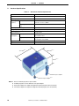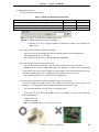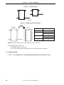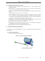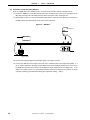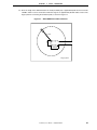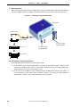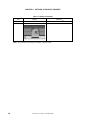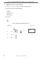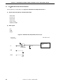
1
To our customers,
Old Company Name in Catalogs and Other Documents
On April 1st, 2010, NEC Electronics Corporation merged with Renesas Technology
Corporation, and Renesas Electronics Corporation took over all the business of both
companies. Therefore, although the old company name remains in this document, it is a valid
Renesas Electronics document. We appreciate your understanding.
Renesas Electronics website: http://www.renesas.com
April 1st, 2010
Renesas Electronics Corporation
Issued by: Renesas Electronics Corporation (http://www.renesas.com)
Send any inquiries to http://www.renesas.com/inquiry.
Notice
1.
2.
3.
4.
5.
6.
7.
All information included in this document is current as of the date this document is issued. Such information, however, is
subject to change without any prior notice. Before purchasing or using any Renesas Electronics products listed herein, please
confirm the latest product information with a Renesas Electronics sales office. Also, please pay regular and careful attention to
additional and different information to be disclosed by Renesas Electronics such as that disclosed through our website.
Renesas Electronics does not assume any liability for infringement of patents, copyrights, or other intellectual property rights
of third parties by or arising from the use of Renesas Electronics products or technical information described in this document.
No license, express, implied or otherwise, is granted hereby under any patents, copyrights or other intellectual property rights
of Renesas Electronics or others.
You should not alter, modify, copy, or otherwise misappropriate any Renesas Electronics product, whether in whole or in part.
Descriptions of circuits, software and other related information in this document are provided only to illustrate the operation of
semiconductor products and application examples. You are fully responsible for the incorporation of these circuits, software,
and information in the design of your equipment. Renesas Electronics assumes no responsibility for any losses incurred by
you or third parties arising from the use of these circuits, software, or information.
When exporting the products or technology described in this document, you should comply with the applicable export control
laws and regulations and follow the procedures required by such laws and regulations. You should not use Renesas
Electronics products or the technology described in this document for any purpose relating to military applications or use by
the military, including but not limited to the development of weapons of mass destruction. Renesas Electronics products and
technology may not be used for or incorporated into any products or systems whose manufacture, use, or sale is prohibited
under any applicable domestic or foreign laws or regulations.
Renesas Electronics has used reasonable care in preparing the information included in this document, but Renesas Electronics
does not warrant that such information is error free. Renesas Electronics assumes no liability whatsoever for any damages
incurred by you resulting from errors in or omissions from the information included herein.
Renesas Electronics products are classified according to the following three quality grades: “Standard”, “High Quality”, and
“Specific”. The recommended applications for each Renesas Electronics product depends on the product’s quality grade, as
indicated below. You must check the quality grade of each Renesas Electronics product before using it in a particular
application. You may not use any Renesas Electronics product for any application categorized as “Specific” without the prior
written consent of Renesas Electronics. Further, you may not use any Renesas Electronics product for any application for
which it is not intended without the prior written consent of Renesas Electronics. Renesas Electronics shall not be in any way
liable for any damages or losses incurred by you or third parties arising from the use of any Renesas Electronics product for an
application categorized as “Specific” or for which the product is not intended where you have failed to obtain the prior written
consent of Renesas Electronics. The quality grade of each Renesas Electronics product is “Standard” unless otherwise
expressly specified in a Renesas Electronics data sheets or data books, etc.
“Standard”:
8.
9.
10.
11.
12.
Computers; office equipment; communications equipment; test and measurement equipment; audio and visual
equipment; home electronic appliances; machine tools; personal electronic equipment; and industrial robots.
“High Quality”: Transportation equipment (automobiles, trains, ships, etc.); traffic control systems; anti-disaster systems; anticrime systems; safety equipment; and medical equipment not specifically designed for life support.
“Specific”:
Aircraft; aerospace equipment; submersible repeaters; nuclear reactor control systems; medical equipment or
systems for life support (e.g. artificial life support devices or systems), surgical implantations, or healthcare
intervention (e.g. excision, etc.), and any other applications or purposes that pose a direct threat to human life.
You should use the Renesas Electronics products described in this document within the range specified by Renesas Electronics,
especially with respect to the maximum rating, operating supply voltage range, movement power voltage range, heat radiation
characteristics, installation and other product characteristics. Renesas Electronics shall have no liability for malfunctions or
damages arising out of the use of Renesas Electronics products beyond such specified ranges.
Although Renesas Electronics endeavors to improve the quality and reliability of its products, semiconductor products have
specific characteristics such as the occurrence of failure at a certain rate and malfunctions under certain use conditions. Further,
Renesas Electronics products are not subject to radiation resistance design. Please be sure to implement safety measures to
guard them against the possibility of physical injury, and injury or damage caused by fire in the event of the failure of a
Renesas Electronics product, such as safety design for hardware and software including but not limited to redundancy, fire
control and malfunction prevention, appropriate treatment for aging degradation or any other appropriate measures. Because
the evaluation of microcomputer software alone is very difficult, please evaluate the safety of the final products or system
manufactured by you.
Please contact a Renesas Electronics sales office for details as to environmental matters such as the environmental
compatibility of each Renesas Electronics product. Please use Renesas Electronics products in compliance with all applicable
laws and regulations that regulate the inclusion or use of controlled substances, including without limitation, the EU RoHS
Directive. Renesas Electronics assumes no liability for damages or losses occurring as a result of your noncompliance with
applicable laws and regulations.
This document may not be reproduced or duplicated, in any form, in whole or in part, without prior written consent of Renesas
Electronics.
Please contact a Renesas Electronics sales office if you have any questions regarding the information contained in this
document or Renesas Electronics products, or if you have any other inquiries.
(Note 1) “Renesas Electronics” as used in this document means Renesas Electronics Corporation and also includes its majorityowned subsidiaries.
(Note 2) “Renesas Electronics product(s)” means any product developed or manufactured by or for Renesas Electronics.
Preliminary User’s Manual
QB-179F124
In-Circuit Emulator
Target Devices
µPD179F110
µPD179F111
µPD179F112
µPD179F122
µPD179F124
Document No. U18586EJ1V0UM00 (1st edition)
Date Published January 2007 NS CP(K)
© NEC Electronics Corporation 2007
Printed in Japan
[MEMO]
2
Preliminary User’s Manual U18586EJ1V0UM
IECUBE is a registered trademark of NEC Electronics Corporation in Japan and Germany.
Windows is either a registered trademark or a trademark of Microsoft Corporation in the United States and/or
other countries.
PC/AT is a trademark of International Business Machines Corporation.
• The information contained in this document is being issued in advance of the production cycle for the
product. The parameters for the product may change before final production or NEC Electronics
Corporation, at its own discretion, may withdraw the product prior to its production.
• No part of this document may be copied or reproduced in any form or by any means without the prior written consent
of NEC Electronics. NEC Electronics assumes no responsibility for any errors that may appear in this document.
• NEC Electronics does not assume any liability for infringement of patents, copyrights or other intellectual property
rights of third parties by or arising from the use of NEC Electronics products listed in this document or any other
liability arising from the use of such products. No license, express, implied or otherwise, is granted under any
patents, copyrights or other intellectual property rights of NEC Electronics or others.
• Descriptions of circuits, software and other related information in this document are provided for illustrative purposes
in semiconductor product operation and application examples. The incorporation of these circuits, software and
information in the design of a customer's equipment shall be done under the full responsibility of the customer. NEC
Electronics assumes no responsibility for any losses incurred by customers or third parties arising from the use of
these circuits, software and information.
(Note)
(1) "NEC Electronics" as used in this statement means NEC Electronics Corporation and also includes its
majority-owned subsidiaries.
(2) "NEC Electronics products" means any product developed or manufactured by or for NEC Electronics (as
defined above).
M5A 06. 2
Preliminary User’s Manual U18586EJ1V0UM
3
[MEMO]
4
Preliminary User’s Manual U18586EJ1V0UM
General Precautions for Handling This Product
1. Circumstances not covered by product guarantee
• If the product was disassembled, altered, or repaired by the customer
• If it was dropped, broken, or given another strong shock
• Use at overvoltage, use outside guaranteed temperature range, storing outside guaranteed temperature range
• If power was turned on while connection to the AC adapter, USB interface cable, or target system was in an
unsatisfactory state
• If the cable of the AC adapter, the USB interface cable, the emulation probe, or the like was bent or pulled
excessively
• If an AC adapter other than the supplied product was used
• If the product got wet
• If this product is connected to the target system when there is a potential difference between the GND of this
product and GND of the target system.
• If the connectors or cables are plugged/unplugged while this product is in the power-on state.
• If excessive load is applied to the connectors or sockets (As for handling, please see 2.5 Mounting and
Connecting Connectors).
• If a metal part of the power switch, cooling fan, or another such part comes in contact with an electrostatic charge.
• If the product is used or stored in an environment where an electrostatic or electrical noise is likely to occur.
2. Safety precautions
• If used for a long time, the product may become hot (50°C to 60°C). Be careful of low temperature burns and
other dangers due to the product becoming hot.
• Be careful of electrical shock. There is a danger of electrical shock if the product is used as described above in
1. Circumstances not covered by product guarantee.
• The AC adapter supplied with the product is exclusively for this product, so do not use it with other products.
Preliminary User’s Manual U18586EJ1V0UM
5
INTRODUCTION
Readers
This manual is intended for users who wish to perform debugging using the QB179F124. The readers of this manual are assumed to be familiar with the device
functions and usage, and to have knowledge of debuggers.
Purpose
This manual is intended to give users an understanding of the basic specifications and
correct usage of the QB-179F124.
Organization
This manual is divided into the following sections.
• General
• Setup procedure
• Settings at product shipment
• Differences between target interface circuit and target device
• Notes
How to Read This Manual
It is assumed that the readers of this manual have general knowledge in the fields of
electrical engineering, logic circuits, and microcontrollers.
This manual describes the basic setup procedures and how to set switches.
To understand the overall functions and usages of the QB-179F124
→ Read this manual in the order of the CONTENTS.
To know the manipulations, command functions, and other software-related settings
of the QB-179F124
→ See the user’s manual of the debugger (supplied with the QB-179F124) to be used.
Conventions
Note:
Footnote for item marked with Note in the text
Caution:
Information requiring particular attention
Remark:
Supplementary information
Numeric representation:
Binary ... xxxx or xxxxB
Decimal ... xxxx
Hexadecimal ... xxxxH
Prefix indicating power of 2
(address space, memory
capacity):
K (kilo): 210 = 1,024
M (mega): 220 = 1,0242
6
Preliminary User’s Manual U18586EJ1V0UM
Terminology
The meanings of the terms used in this manual are described in the table below.
Term
Target device
Target system
Meaning
This is the device to be emulated.
This is the system to be debugged.
This includes the target program and the hardware provided by the user.
IECUBE
TM
Generic name for NEC Electronics’ high-performance/compact in-circuit
emulator.
Related Documents
Please use the following documents in conjunction with this manual.
The related documents listed below may include preliminary versions. However,
preliminary versions are not marked as such.
Documents Related to Development Tools (User’s Manuals)
Document Name
QB-179F124 In-Circuit Emulator
RA78K0 Assembler Package Ver. 3.80
CC78K0 C Compiler Ver. 3.70
ID78K0-QB Integrated Debugger Ver. 2.94
This manual
Operation
U17199E
Language
U17198E
Structured Assembly Language
U17197E
Operation
U17201E
Language
U17200E
Operation
U18330E
PM plus Ver. 5.20
Caution
Document Number
U16934E
The related documents listed above are subject to change without notice. Be sure to use the latest
version of each document for designing, etc.
Preliminary User’s Manual U18586EJ1V0UM
7
CONTENTS
CHAPTER 1 GENERAL............................................................................................................................. 9
1.1
Hardware Specifications ................................................................................................................................10
1.2
System Specifications....................................................................................................................................11
1.3
System Configuration ....................................................................................................................................12
1.4
System Configuration for Each Target Device.............................................................................................13
1.5
Package Contents ..........................................................................................................................................14
CHAPTER 2 SETUP PROCEDURE ....................................................................................................... 15
2.1
Names and Functions of Hardware...............................................................................................................16
2.2
Removal of Acrylic Board ..............................................................................................................................18
2.3
Clock Settings.................................................................................................................................................18
2.3.1 Overview of clock settings ..................................................................................................................18
2.4
Software Settings ...........................................................................................................................................20
2.5
Mounting and Connecting Connectors ........................................................................................................21
2.5.1 Mounting TC to target system .............................................................................................................21
2.5.2 Mounting YQ to TC ...............................................................................................................................21
2.5.3 Plugging EA into YQ ............................................................................................................................22
2.5.4 Precautions for handling TC, YQ, SA, and CA ...................................................................................22
2.5.5 Precautions for mounting IC using TC and MA .................................................................................23
2.6
Connecting QB-179F124 to Target System ..................................................................................................23
2.7
Notes on Power Supply and GND Pin Connection ......................................................................................27
2.8
Connecting USB Interface Cable and AC Adapter.......................................................................................27
2.9
Switching Power On and Off .........................................................................................................................27
CHAPTER 3 SETTINGS AT PRODUCT SHIPMENT........................................................................... 28
CHAPTER 4 DIFFERENCES BETWEEN TARGET INTERFACE CIRCUIT AND TARGET
DEVICE ............................................................................................................................... 29
4.1
For µ PD179F110, 179F111, and 179F112 Emulation...................................................................................30
4.2
For µ PD179F122 and 179F124 Emulation ....................................................................................................32
CHAPTER 5 NOTES................................................................................................................................ 34
8
Preliminary User’s Manual U18586EJ1V0UM
CHAPTER
1
GENERAL
The QB-179F124 is an in-circuit emulator for emulating the µ PD179F11x and 179F12x.
Hardware and software can be debugged efficiently in the development of systems in which the µ PD179F11x and
179F12x are used.
This manual descries basic setup procedures, hardware specifications, system specifications,
and how to set switches.
Preliminary User’s Manual U18586EJ1V0UM
9
CHAPTER 1
1.1
GENERAL
Hardware Specifications
Table 1-1. QB-179F124 Hardware Specifications
Parameter
Specification
Target device
µ PD179F110, 179F111, 179F112, 179F122, 179F124
Operating voltage
1.8 to 3.6 V
Operating
frequency
Main system clock
2.7 V ≤ VDD ≤ 3.6 V: 1 to 10 MHz
1.8 V ≤ VDD < 2.7 V: 1 to 5 MHz
Internal high-speed oscillation
clock
1.8 V ≤ VDD ≤ 3.6 V: 4 MHz TYP.
Operating temperature range
0 to 40°C (No condensation)
Storage temperature range
−15 to 60°C (No condensation)
External dimensions
See figure below
Power
consumption
AC adapter for QB-179F124
Output: DC15 V, 1 A
Input: AC100 to 240 V
Target system power supply
Voltage: 1.8 to 3.6 V
Current: approx. 275 µ A MAX.
Weight
Approx. 400 g
Host interface
USB interface (1.1, 2.0)
112.7 mmNote 1
108.2 mmNote 2
58 mmNote 3
Rear space adapter
Front space adapterNote 4
Notes 1. Does not include projection of power switch
2. Includes projection of screw that fixes rear space adapter
3. Rear space adapter can adjust the height from 30 mm (longest) to 0 mm (shortest)
4. Front space adapter can adjust the height from 20 mm (longest) to 5 mm (shortest)
10
Preliminary User’s Manual U18586EJ1V0UM
CHAPTER 1
1.2
GENERAL
System Specifications
This section shows the QB-179F124 system specifications.
Table 1-2. System Specifications
Parameter
Emulation memory capacity
Program execution
functions
Specification
Internal ROM
512 KB (MAX.)
Internal RAM
61.75 KB (MAX.)
Real-time execution function
Go, Start from Here, Come Here, Restart, Return Out,
Ignore break points and Go
Non-real-time execution function
Step In, Next Over, Slowmotion, Go & Go
Memory manipulation
Available (initialize, copy, compare)
Register manipulation
Available (general-purpose registers, control registers, SFRs)
Disassemble function
Available
Local variable view
Local variables
Watch data view
Local variables, global variables, or else
Stack trace view
Available
Break functions
Trace functions
Event break
Execution: 8 points
Access: 8 points
Software break
2000 points
Pre-execution break
4 to 8 points
Fail-safe break
Non-map, write protect, SFR illegal access, stack overflow, or else
Other
Forcible break, trace full break, trace delay break, timeout break,
timer overflow break
Trace data types
Program address, program data, access address, access data,
status, time tag
Trace modes
Unconditional trace, section trace, qualify trace, delay trigger trace
Trace functions
Non-stop, full stop, full break, delay trigger stop, delay trigger
break
Memory capacity
128K frames
Note
Real-time RAM monitoring function
All internal RAM spaces
Time measurement
functions
Measurement clock
60 MHz
Measurement objects
Start through end of program execution
Start event through end event
Maximum measurement time
Approx. 40 hours and 43 minutes (Resolution: 17 ns)
Number of timers for
measurement
Start through end of program execution: 1
Start event through end event: 2
Measurement results
Execution time (start through end of execution)
Maximum, minimum, average, total, pass count (between events)
Other
Other functions
Timer overflow break function, timeout break function
Command functions set in the console, mapping function, event
function, coverage function, snapshot function, DMM function,
power-off emulation function, pin mask function, flash self
programming emulation function
Note The number of breaks that can be set varies depending on the location where the break is set.
Preliminary User’s Manual U18586EJ1V0UM
11
CHAPTER 1
1.3
GENERAL
System Configuration
This section shows the system configuration when using the QB-179F124 connected to a PC (Windows
TM
(Windows 2000 and Windows XP), PC/AT
compatible).
TM
PC
Connection is possible even without optional products.
Figure 1-1. System Configuration
<1>
<3>
<5>
<4>
<2>
<6>
<7>
<8>
<12>
<13>
<9>
<10>
<11>
<14>
<1> Host machine
<2> ID78K0-QB Disk/Accessory Disk
<3> USB interface cable
<4> AC adapter
<5> QB-179F124
<6> Check pin adapter (optional)
<7> Emulation probe
<8> Exchange adapter
<9> Space adapter (optional)
<10> YQ connector
<11> Target connector
<12> Mount adapter (optional)
<13> Device
<14> Target system
: Windows PC (Windows 2000 and Windows XP), IBM PC/AT compatible
can be used
: Debugger, USB drivers, manual, etc.
: Cable connecting QB-179F124 to host machine
: Support input AC100 to 240 V
: This product
: Adapter used for monitoring waveforms with oscilloscope
: Flexible type of emulation probe
: Adapter that performs pin conversion
: Adapter used for height adjustment
: Connector that connects exchange adapter to target connector
: Connector soldered to target system
: Adapter used for mounting target device into socket
: Target device
Remarks 1. Obtain device files from the NEC Electronics website.
http://www.necel.com/micro/ods/eng/
2. Refer to 1.5 Package Contents for the purchase forms of the above products.
3. As for handling of connectors, refer to 2.5 Mounting and Connecting Connectors.
12
Preliminary User’s Manual U18586EJ1V0UM
CHAPTER 1
1.4
GENERAL
System Configuration for Each Target Device
The following table lists the system configuration for each target device of the QB-179F124.
Table 1-3. Adapters and Connectors for Each Target Device
Target
Device
Package
µ PD179F110, 30MC
179F111,
179F112
µ PD179F122, 38MC
179F124
Exchange Adaptor
Space Adaptor
YQ Connector
Target Connector
Mount Adaptor
QB-30MC-EA-02T
Note
(sold separately)
QB-30MC-YS-01T
(sold separately)
QB-30MC-YQ-01T
Note
(sold separately)
QB-30MC-NQ-01T
Note
(sold separately)
QB-30MC-HQ-01T
(sold separately)
QB-38MC-EA-02T
Note
(sold separately)
QB-38MC-YS-01T
(sold separately)
QB-38MC-YQ-01T
Note
(sold separately)
QB-38MC-NQ-01T
Note
(sold separately)
QB-38MC-HQ-01T
(sold separately)
Table 1-4. Common Probe and Adapter
Name
Note
Part Number
Check pin adapter
QB-144-CA-01 (sold separately)
Emulation probe
QB-80-EP-01T (sold separately)
Note
These items are included with the QB-179F124, depending on the ordering code.
• If QB-179F124-ZZZ is ordered
The exchange adapter, YQ connector, target connector and emulation probe are not included.
• If QB-179F124-T30MC is ordered
The QB-30MC-EA-02T, QB-30MC-YQ-01T, QB-30MC-NQ-01T and QB-80-EP-01T are included.
• If QB-179F124-T38MC is ordered
The QB-38MC-EA-02T, QB-38MC-YQ-01T, QB-38MC-NQ-01T and QB-80-EP-01T are included.
Remark For notes on target system design and package drawings, refer to [Related Information] on the following
URL.
http://www.necel.com/micro/english/iecube/index.html
Preliminary User’s Manual U18586EJ1V0UM
13
CHAPTER
1.5
1
GENERAL
Package Contents
The following items have been placed in the QB-179F124 packing box.
Please check the contents.
Products supplied with QB-179F124-ZZZ
1:
QB-179F124
2:
AC adapter
3:
USB interface cable (2 meters)
4:
Online user registration card (warranty card and software contract in one)
5:
ID78K0-QB Disk (CD-ROM)
6:
Accessory Disk (CD-ROM)
7:
IECUBE Setup Manual (Japanese/English)
8:
Packing list
9:
QB-MINI2
Products supplied with QB-179F124-T30MC
1 to 9
10:
Emulation probe
11:
Exchange adapter
12:
YQ connector
13:
Target connector
QB-80-EP-01T
QB-30MC-EA-02T
QB-30MC-YQ-01T
QB-30MC-NQ-01T
Products supplied with QB-179F124-T38MC
1 to 9
14
10:
Emulation probe
11:
Exchange adapter
12:
YQ connector
13:
Target connector
QB-80-EP-01T
QB-38MC-EA-02T
QB-38MC-YQ-01T
QB-38MC-NQ-01T
Preliminary User’s Manual U18586EJ1V0UM
CHAPTER 2
SETUP
PROCEDURE
This chapter explains the QB-179F124 setup procedure.
Setup can be completed by performing installation setup in the order in which it appears in this chapter.
Perform setup along the lines of the following procedure.
See 2.1
Names and Functions of Hardware for clock positions.
Clock settings
Hardware settings are not required if the clock internally generated from the emulator is used.
If an oscillator must be mounted, see 2.2
Removal of Acrylic Board and 2.3 Clock Settings.
Software settings
See 2.4
Software Settings.
Mounting and connecting connectors
See 2.5
Mounting and Connecting Connectors.
Connecting QB-179F124 to target system
See 2.6 Connecting QB-179F124 to Target System.
Connecting USB interface cable and AC adapter
See 2.8 Connecting USB Interface Cable and AC Adapter.
Switching power on and off
See 2.9
Switching Power On and Off.
Preliminary User’s Manual U18586EJ1V0UM
15
CHAPTER
2
SETUP
PROCEDURE
2.1 Names and Functions of Hardware
Figure 2-1. Names of Parts of QB-179F124
Top View
Bottom View
Power switch
OSC1
CN4
POWER
TARGET
TCN2
TCN1
Side View
Power supply connector
USB connector
16
Preliminary User’s Manual U18586EJ1V0UM
CHAPTER
2
SETUP
PROCEDURE
(1) TCN1, TCN2
These are connectors for connecting a check pin adapter or emulation probe.
(2) OSC1
This is a socket for mounting the oscillator.
(3) CN4
This is a connector for the shipment inspection. It is not something that the user will need.
(4) POWER (Red LED)
This is an LED that shows whether the power supply of the QB-179F124 is switched on.
LED State
QB-179F124 State
Lit
Power switch ON
Not lit
Power switch OFF or AC adapter not connected to QB-179F124
Blinking
Internal error occurred (Contact an NEC Electronics sales representative or
distributor)
(5) TARGET (Green LED)
This is an LED that shows whether the power supply of the target system is switched on.
LED State
Target System State
Lit
Target system power supply ON
Not lit
Target system power supply OFF or target system not connected
(6) Power switch
This is the power switch of the QB-179F124.
It is OFF at shipment.
Preliminary User’s Manual U18586EJ1V0UM
17
CHAPTER
2.2
2
SETUP
PROCEDURE
Removal of Acrylic Board
To modify the clock setting, the acrylic board on the bottom of the QB-179F124 must be removed.
The acrylic board can be removed by lifting it up.
Figure 2-2.
2.3
Acrylic Board Removal Method
Clock Settings
2.3.1 Overview of clock settings
The following three types of clock settings are available.
Each clock setting is listed below.
Clock Used
(1) High-speed system clock
(2) Internal high-speed
oscillation clock
Debugger Setting
(in Configuration Dialog)
Clock Supply
Uses the clock internally generated from the emulator
System
Uses the square-wave clock from the target system
External
Uses the clock generated from the oscillator (OSC1)
mounted on the emulator
Clock Socket
Uses the clock internally generated from the emulator
–
Oscillation with the resonator on the target system is not supported.
Therefore, the in-circuit emulator cannot
emulate the oscillation operation of the clock on the target system.
18
Preliminary User’s Manual U18586EJ1V0UM
CHAPTER
2
SETUP
PROCEDURE
(1) High-speed system clock
The clock settings are listed below.
Table 2-1. Settings for High-Speed System Clock
Type of Clock to Be Used
OSC1
(a) Uses the clock internally generated from the emulator
(b) Uses the square-wave clock from the target system
–
Note
(c) Uses the clock generated from the oscillator (OSC1) mounted on the emulator
–
Oscillator mounted
Debugger Setting
System
External
Clock Socket
Note This setting is not possible when TARGET LED is not lit.
Remarks 1. Settings other than the above are prohibited.
2. Selection of (a) or (b) is possible regardless of whether the oscillator is not mounted in the
OSC1socket.
(a) Uses the clock internally generated from the emulator
Select the “System” in the debugger and select the desired frequency from the drop-down list.
The following frequencies are selectable.
2.00, 3.00, 3.57, 4.00, 4.19, 4.91, 5.00, 6.00, 8.00, 8.38, 10.00 [MHz]
(b) Uses the square-wave clock from the target system
Select the “External” in the debugger. The clock input from the target system is then used.
Oscillation with the resonator on the target system is not supported. To input a clock from the target
system, input to the clock pin (X2) the square-wave signal with the same voltage potential as that of the
target device supply voltage (VDD). Inputting the inverted signal to X1 is not necessary.
The selectable frequencies are same as those of the target device.
(c) Uses the clock generated from the oscillator (OSC1) mounted on the emulator
Mount an oscillator in the OSC1 socket in the emulator and then select the “Clock socket” in the
debugger. The clock generated from the oscillator mounted on the emulator is used.
The selectable frequencies are same as those of the target device.
Note
As an oscillator
to be mounted in the OSC1 socket in the emulator, use the one that satisfies the
following specifications.
- Supply voltage: 5 V
- Output level: CMOS
Note An oscillator that uses a resonator cannot be used.
Preliminary User’s Manual U18586EJ1V0UM
19
CHAPTER
2
SETUP
PROCEDURE
Figure 2-3. Oscillator Shape
Top View
Figure 2-4.
Oscillator
Mapping of Oscillator to Socket
Socket
Oscillator
VCC
NC
GND
CLOCK OUT
OSC1 Pin Number
1
14
NC
1
2
13
GND
4
3
12
4
11
5
10
6
9
7
8
7
CLOCK OUT
8
11
VCC
14
Remark Insert the oscillator into the socket, take care for the pin 1 position.
(2) Internal high-speed oscillation clock
The debugger setting is not necessary.
The use of the internal high-speed oscillation clock can be specified in the user program.
2.4
Software Settings
For details, see the ID78K0-QB Ver. 2.94 Integrated Debugger Operation User's Manual (U18330E).
20
Preliminary User’s Manual U18586EJ1V0UM
CHAPTER
2.5
2
SETUP
PROCEDURE
Mounting and Connecting Connectors
This section describes the methods of connecting the QB-179F124 and target system.
Make connections with both the QB-179F124 and target system powered OFF.
The following abbreviations are used in this section:
- TC: Target connector
- YQ: YQ connector
- EA: Exchange adapter
- MA: Mount adapter
- CA: Check pin adapter
- SA: Space adapter
2.5.1 Mounting TC to target system
(1) Thinly apply a two-component epoxy adhesive (hardening time at least 30 minutes) to the ends of the four
projections on the base of the TC and adhere the TC to the user board (clean the surface of the target
system board using alcohol or the like). If alignment of target system pads to TC leads is difficult, align
them as in (2).
(2) Align by inserting the guide pins for alignment for the TC (NQGUIDE) through the pin holes on the top of
the TC. Accessory holes are φ1.0 mm non-through holes in two or three places.
(For hole positions, see the particular TC drawing.)
(3) Solder after fitting the MA to the TC. This is to prevent troubles such as flux or solder splashing and
adhering to the TC contact pins when soldering.
- Soldering conditions
Caution
Solder reflow
260°C × 10 seconds or less
Manual soldering
350°C × 5 seconds or less (1 pin)
Do not perform washing by flux immersion or vapor.
(4) Take away the guide pins.
2.5.2
Mounting YQ to TC
(1) After confirming that there are no broken or bent YQ contact pins, fit the YQ in the TC and fasten the screw.
If repeatedly inserting and removing, be sure to inspect the YQ pins before fitting. If pins are bent, correct
them using something thin and flat such as the edge of a knife.
(2) Accessory holes are needed in prescribed positions in four places in the board for connecting the YQ.
Fasten the YQ to the TC on the target system using the supplied M2 x 10 mm screws. The thickness of a
board corresponding to these screws is 1.0 to 2.0 mm.
Fasten the screws equally in the four corners
using a #0 or #1 Phillips precision screwdriver or torque driver. The tightening torque of the screws is
0.054 Nm (MAX.). Too great tightening causes bad connections.
Four screws for fitting to the TC (M2 x 10 mm / 4 units) are included with the YQ.
Preliminary User’s Manual U18586EJ1V0UM
21
CHAPTER
2.5.3
2
SETUP
PROCEDURE
Plugging EA into YQ
Match the pin 1 position of the YQ or SA (corner cuts match in both) to the pin 1 position of the EA and plug
in.
- When plugging or unplugging, press on the TC, YQ, and SA with a finger so that there is no force on the
TC.
- When plugging or unplugging, be careful of the direction of wiggling.
As a tool when unplugging, insert some kind of thin non-conductive material such as a wooden stick between
the YQ (SA) and EA and wiggle while slowly unplugging.
Be careful since the connector will be damaged if
this is done in the wrong direction.
2.5.4 Precautions for handling TC, YQ, SA, and CA
(1) When taking the TC from the box, press down on the body and take out the sponge first.
(2) Since the pins of the YQ are thin and easily bent, be careful. When inserting it in the TC, confirm that there
are no bent pins.
(3) When screwing a YQ soldered to a board to the TC, fasten the screws in four places in turn using a #0 or
#1 Phillips precision screwdriver or torque driver after tentatively tightening them. Fix the torque at 0.054
Nm (MAX.).
If just one place is overtightened, it may cause poor contact. Moreover, a board being connected to the
YQ must have accessory holes in prescribed positions (four places: φ2.3 mm or φ3.3 mm). The φ3.8 mm
or φ4.3 mm that is the screw head size is an area where wiring is prohibited.
(4) In YQ and SA removal, since there is a danger of YQ pins being bent or broken when prying and wiggling,
remove them gradually using a flatbladed screwdriver from four directions.
Moreover, to connect and use
the YQ and SA, screw the YQ to the TC according to the YQGUIDE (included with the YQ) using a 2.3 mm
flatbladed screwdriver and then connect it to the SA.
Fix the torque at 0.054 Nm (MAX.). If even one
place is overtightened, it may cause poor contact.
(5) For the TC, YQ, and SA, since there is a danger that washing fluid on the structure will remain in the
connector, do not perform washing.
(6) TC, IC, and YQ cannot be used in combination.
(7) A TC/YQ system cannot be used in an environment of vibrations or shocks.
(8) It is assumed that this product will be used in system development and evaluation.
Moreover, when used
in Japan, Electrical Appliance and Material Control Law and electromagnetic disturbance countermeasures
have not been applied.
(9) Since there are rare cases of shape change if the box is left for a long time in a place where it is 50°C or
higher, for safekeeping, store it in a place where it is no higher than 40°C and direct sunlight does not hit it.
(10) For details about handling the TC, YQ, and SA, see the NQPACK series technical materials at the website
of Tokyo Eletech Corporation.
URL: http://www.tetc.co.jp/
(11) CA
The CA is an optional product for IECUBE, and can be used to measure the waveform between IECUBE
and the target system.
Since the pins on the CA do not correspond to the pin layout in each device, the pin header cover must be
mounted according to the device to be used. For mounting methods of the pin header cover, refer to
[Related Information] on the following URL.
http://www.necel.com/micro/english/iecube/index.html
22
Preliminary User’s Manual U18586EJ1V0UM
CHAPTER
2
SETUP
PROCEDURE
2.5.5 Precautions for mounting IC using TC and MA
(1) Confirm that there is no weld flash in the resin (sealant part) of the IC. If there is weld flash, remove it
using a knife or the like.
(2) Confirm that there is no weld flash breaking or bending of IC leads.
In particular, confirm the planarity of
IC leads. If there is abnormality in the planarity, correct that portion.
(3) Viewing the TC contact pins from the top, if there are foreign bodies on them, remove them using a brush or
the like.
After confirming (1) to (3), fit the IC to the TC. Also fit the MA.
(4) Put the supplied M2 x 6 mm screws in the four accessory holes of the MA and fasten the screws in opposite
corners. At that time, use either the dedicated screwdriver that is supplied or a torque driver to fasten
them equally in turn with a tightening torque of 0.054 Nm (MAX.). Since the contact is poor if tightening is
too great, once you have lightly fastened the MA screws, tighten them again.
(5) Depending on the use environment, when starting up a device that has been left for a long time, starting it
may be difficult. In this case, loosen the screws slightly and then retighten them.
(6) If startup still is difficult after (5) above, check (1) to (3) again.
(7) Tightening the screws of the MA too much may give rise to cracks in the molded part of the MA (plastic
part) and bend the mold into a bowed shape, making contact poor.
(8) After soldering the TC, do not perform cleaning by flux immersion or vapor.
2.6
Connecting QB-179F124 to Target System
If connecting the emulation probe (QB-80-EP-01T), connect it to the QB-179F124 and the target system by the
following procedure.
(a) Connection of emulation probe
Connect the emulation probe to the QB-179F124.
Figure 2-5. Emulation Probe Connection Method
Insert CN1 and CN2 of the probe into
TCN1 and TCN2 of the QB-179F124.
Preliminary User’s Manual U18586EJ1V0UM
23
CHAPTER
2
SETUP
PROCEDURE
(b) Connection of emulation probe GND wire
There are 2 GND wires in the emulation probe. Connect them to the QB-179F124 and target system.
<1> Fasten the GND wire on the QB-179F124 side of the emulation probe to the nut on the bottom of the
QB-179F124 using a #0 or #1 Phillips precision driver (connection of B to A in Figure 2-6).
<2> Next plug the connector on top of the emulation probe into the connector at the opening on the bottom of
the QB-179F124 from below being careful of the insertion direction.
Figure 2-6. GND Wire
QB-179F124
A
B
C
Target system
<3> Connect the exchange adapter and emulation probe to the target connector.
<4> Connect the GND wire on the target system side of the emulation probe to the target system GND.
If a
pin or screw is fastened to the target system GND, remove the transparent terminal cover on the end of
the GND wire and fasten the Y terminal of the GND wire to the target system (C in Figure 2-6).
If the
GND on the target system is an exposed pad, likewise fasten the Y terminal to the pad on the target
system by soldering (recommended soldering iron temperature setting:
24
Preliminary User’s Manual
U18586EJ1V0UM
300°C).
CHAPTER
2
SETUP
PROCEDURE
<5> Since the length of the GND wire below the head (insulated part) is approximately 60 mm, there must be
a GND to which it can be connected to within the range of an approximately 60 mm radius section of the
target system for connecting the emulation probe, as shown in Figure 2-7.
Figure 2-7. Where GND Wire Can Be Connected
20
L = 60
27.5
30.75
Target system
Preliminary User’s Manual U18586EJ1V0UM
25
CHAPTER
2
SETUP
PROCEDURE
(c) Ensuring isolation
When connecting the target system to the QB-179F124 using an emulation probe, adjust the height using the
front space adapter or rear space adapter of the QB-179F124 and ensure isolation from the target system.
Figure 2-8. Connection Using Emulation Probe
QB-179F124
Emulation probe
Exchange adapter
Rear space adapter
(Height adjustable)
YQ connector
Front space adapter
(Height adjustable)
Target connector
(d) Precautions related to emulation probe
The following precautions pertain to using the emulation probe.
<1> Be careful that stress of the emulation probe is not placed on the target connector. Moreover, when
removing the emulation probe, remove it slowly while pressing down on the exchange adapter with a
finger so that there is no stress on the target connector.
<2> Be sure to connect the GND wire of the emulation probe to the QB-179F124 and the target system. If
not, the impedance of the cable becomes unstable, resulting in the lowering of signal transmission
characteristics or distortion of the output waveform for an input waveform.
26
Preliminary User’s Manual U18586EJ1V0UM
CHAPTER
2.7
2
SETUP
PROCEDURE
Notes on Power Supply and GND Pin Connection
For power supplies and GND pins of the target device, be sure to connect all pins to each power supply or GND.
2.8
Connecting USB Interface Cable and AC Adapter
Plug the USB interface cable supplied with the QB-179F124 into the USB connector of the host machine, and
plug the other side into the USB connector on the rear of the QB-179F124.
Plug the AC adapter supplied with the QB-179F124 into a receptacle and plug the other side into the power
supply connector on the rear of the QB-179F124.
For QB-179F124 connector positions, see Figure 2-9.
Figure 2-9. Connector Positions
Power supply connector
(Connect AC adapter)
USB connector
(Connect USB interface cable)
2.9
Switching Power On and Off
Be sure to switch the power on and off according to the following procedures.
- Switching power on
- Switching power off
<1> QB-179F124 power on
<1> Debugger termination
Note
Note
<2> Target system power on
<2> Target system power off
<3> Debugger startup
<3> QB-179F124 power off
Note In the procedures, <2> is unnecessary if the target system is not connected.
Caution
If the wrong sequence was used for the operation, the target system or QB-179F124 may fail.
Preliminary User’s Manual U18586EJ1V0UM
27
CHAPTER 3 SETTINGS AT PRODUCT SHIPMENT
Table 3-1. Settings at Shipment
Setting
Item
OSC1
Power switch
Not mounted
Remarks
Note
Oscillator can be mounted
Set to OFF at shipment.
Note The oscillation circuit using an oscillation cannot be used.
28
Preliminary User’s Manual U18586EJ1V0UM
.
CHAPTER 4 DIFFERENCES BETWEEN TARGET INTERFACE CIRCUIT AND TARGET DEVICE
This chapter explains the differences between the signal lines of a target interface circuit of the QB-179F124 and
the signal lines of a target device
Although the target device is a CMOS circuit, the target interface circuit of the QB-179F124 consists of an
emulation circuit that depends on the emulation CPU, TTL, CMOS-IC, or other.
When the target system is debugged by connecting it to the QB-179F124, the QB-179F124 emulates just as if the
actual target device were operating on the target system.
However, small differences arise because the QB-179F124 actually is emulating.
(1) Signals input and output by emulation CPU (FPGA)
(2) Other signals
The circuits of the QB-179F124 for the signals in (1) and (2) above are shown below by target device.
Preliminary User’s Manual U18586EJ1V0UM
29
CHAPTER 4 DIFFERENCES BETWEEN TARGET INTERFACE CIRCUIT AND TARGET DEVICE
4.1
For µ PD179F110, 179F111, and 179F112 Emulation
For the signals in (1) and (2) below, see Figure 4-1 Emulation Circuit Equivalent Circuit 1.
(1) Signals input and output by emulation CPU (FPGA)
• P07 to P00
• P17 to P10
• P27 to P25, P22 to P20
• P122 to P120
• RESETN, FLMD0
(2) Other signals
• VDD
• GND
• REGC
Figure 4-1. Emulation Circuit Equivalent Circuit 1 (1/2)
• Probe side
(target system)
• QB-179F124 side
VDD
Emulation power
supply
VDD
PI5A4624TEX
0.1 µ F
GND
REGC
Open
30
Preliminary User’s Manual U18586EJ1V0UM
CHAPTER 4 DIFFERENCES BETWEEN TARGET INTERFACE CIRCUIT AND TARGET DEVICE
Figure 4-1. Emulation Circuit Equivalent Circuit 1 (2/2)
• Probe side
(target system)
• QB-179F124 side
LVDD
Pull-up Control IC
150 kΩ
P07
P17 to P10
FPGA Emulation CPU
30 Ω
Level Shifter
P00 to P06
P27 to P25,
P22 to P20
P122 to P120
30 Ω
Level Shifter
LVDD
Pull-up Control IC
150 kΩ
Level Shifter
RESETN
1 MΩ
Level Shifter
Level Shifter
4.7 kΩ
15 kΩ
Level Shifter
FLMD0
15 kΩ
Level Shifter
Level Shifter
Preliminary User’s Manual U18586EJ1V0UM
31
CHAPTER 4 DIFFERENCES BETWEEN TARGET INTERFACE CIRCUIT AND TARGET DEVICE
4.2
For µ PD179F122 and 179F124 Emulation
For the signals in (1) and (2) below, see Figure 4-2 Emulation Circuit Equivalent Circuit 2.
(1) Signals input and output by emulation CPU (FPGA)
• P07 to P00
• P17 to P10
• P27 to P20
• P35 to P30
• P122 to P120
• RESETN, FLMD0
(2) Other signals
• VDD
• GND
• REGC
Figure 4-2. Emulation Circuit Equivalent Circuit 2 (1/2)
• Probe side
(target system)
• QB-179F124 side
VDD
Emulation power
supply
VDD
PI5A4624TEX
0.1 µ F
GND
REGC
Open
32
Preliminary User’s Manual U18586EJ1V0UM
CHAPTER 4 DIFFERENCES BETWEEN TARGET INTERFACE CIRCUIT AND TARGET DEVICE
Figure 4-2. Emulation Circuit Equivalent Circuit 2 (2/2)
• Probe side
(target system)
• QB-179F124 side
LVDD
Pull-up Control IC
150 kΩ
P07
P17 to P10
P35 to P30
FPGA Emulation CPU
30 Ω
Level Shifter
30 Ω
P00 to P06
P27 to P20
P122 to P120
Level Shifter
LVDD
Pull-up Control IC
150 kΩ
Level Shifter
RESETN
1 MΩ
Level Shifter
Level Shifter
4.7 kΩ
15 kΩ
Level Shifter
FLMD0
15 kΩ
Level Shifter
Level Shifter
Preliminary User’s Manual U18586EJ1V0UM
33
CHAPTER 5 NOTES
Observe the following notes.
• Even when using the product without connecting a target system, connect and use the emulation probe and
exchange adapter.
If the product is used without connecting the emulation probe and exchange adapter, a warning window is
displayed but use is possible.
• Do not turn off the target power supply (do not allow it to become lower than the POC voltage) during a break
(power supply can be turned off only during RUN).
• When inputting the external clock, input the square waveform with the same potential as the target device to the
clock pins (X2).
• A WDT reset is not generated when an area for which the capacities of the internal ROM, internal high-speed
ROM, and internal expansion RAM are not set with the IMS and IXS registers is illegally accessed. Emulation is
performed with a fail-safe break.
• An internal oscillator of IECUBE is used as the high-speed internal oscillator. Thus, because trimming is not
required, the high-speed internal oscillator trimming register (R4MTRM2) cannot be emulated and actual
operation is not affected by accessing the high-speed internal oscillator trimming register (R4MTRM2).
• The REGC pin is processed within IECUBE and is not connected externally. Thus the REGC pin cannot be
emulated.
• If the power supply of the target system is OFF, even though IECUBE and the target system are connected, no
warning message will be displayed even if the debugger is started with “Target” setting set to “Not Connect”.
34
Preliminary User’s Manual U18586EJ1V0UM
For further information,
please contact:
NEC Electronics Corporation
1753, Shimonumabe, Nakahara-ku,
Kawasaki, Kanagawa 211-8668,
Japan
Tel: 044-435-5111
http://www.necel.com/
[America]
[Europe]
[Asia & Oceania]
NEC Electronics America, Inc.
2880 Scott Blvd.
Santa Clara, CA 95050-2554, U.S.A.
Tel: 408-588-6000
800-366-9782
http://www.am.necel.com/
NEC Electronics (Europe) GmbH
Arcadiastrasse 10
40472 Düsseldorf, Germany
Tel: 0211-65030
http://www.eu.necel.com/
NEC Electronics (China) Co., Ltd
7th Floor, Quantum Plaza, No. 27 ZhiChunLu Haidian
District, Beijing 100083, P.R.China
Tel: 010-8235-1155
http://www.cn.necel.com/
Hanover Office
Podbielskistrasse 166 B
30177 Hannover
Tel: 0 511 33 40 2-0
Munich Office
Werner-Eckert-Strasse 9
81829 München
Tel: 0 89 92 10 03-0
Stuttgart Office
Industriestrasse 3
70565 Stuttgart
Tel: 0 711 99 01 0-0
United Kingdom Branch
Cygnus House, Sunrise Parkway
Linford Wood, Milton Keynes
MK14 6NP, U.K.
Tel: 01908-691-133
Succursale Française
9, rue Paul Dautier, B.P. 52
78142 Velizy-Villacoublay Cédex
France
Tel: 01-3067-5800
Sucursal en España
Juan Esplandiu, 15
28007 Madrid, Spain
Tel: 091-504-2787
NEC Electronics Shanghai Ltd.
Room 2511-2512, Bank of China Tower,
200 Yincheng Road Central,
Pudong New Area, Shanghai P.R. China P.C:200120
Tel: 021-5888-5400
http://www.cn.necel.com/
NEC Electronics Hong Kong Ltd.
12/F., Cityplaza 4,
12 Taikoo Wan Road, Hong Kong
Tel: 2886-9318
http://www.hk.necel.com/
NEC Electronics Taiwan Ltd.
7F, No. 363 Fu Shing North Road
Taipei, Taiwan, R. O. C.
Tel: 02-8175-9600
http://www.tw.necel.com/
NEC Electronics Singapore Pte. Ltd.
238A Thomson Road,
#12-08 Novena Square,
Singapore 307684
Tel: 6253-8311
http://www.sg.necel.com/
NEC Electronics Korea Ltd.
11F., Samik Lavied’or Bldg., 720-2,
Yeoksam-Dong, Kangnam-Ku,
Seoul, 135-080, Korea
Tel: 02-558-3737
http://www.kr.necel.com/
Tyskland Filial
Täby Centrum
Entrance S (7th floor)
18322 Täby, Sweden
Tel: 08 638 72 00
Filiale Italiana
Via Fabio Filzi, 25/A
20124 Milano, Italy
Tel: 02-667541
Branch The Netherlands
Steijgerweg 6
5616 HS Eindhoven
The Netherlands
Tel: 040 265 40 10
G06.11A