1
www.dbebooks.com - Free Books & magazines
RAPID PROTOTYPING
O F D I G I TA L S Y S T E M S
SOPC EDITION
RAPID PROTOTYPING
O F D I G I TA L S Y S T E M S
SOPC EDITION
James O. Hamblen
School of Electrical and Computer Engineering
Georgia Institute of Technology
Tyson S. Hall
School of Computing
Southern Adventist University
Michael D. Furman
Department of Engineering
Cambridge University
James O. Hamblen
Georgia Institute of Technology
Atlanta, GA
Tyson S. Hall
Southern Adventist University
Collegedale, TN
Michael D. Furman
University of Florida
Gainesville, FL
Library of Congress Control Number: 2007934543
ISBN 978-0-387-72670-0
e-ISBN 978-0-387-72671-7
Printed on acid-free paper.
© 2008 Springer Science+Business Media, LLC
All rights reserved. This work may not be translated or copied in whole or in part without the written permission of
the publisher (Springer Science+Business Media, LLC, 233 Spring Street, New York, NY 10013, USA), except for
brief excerpts in connection with reviews or scholarly analysis. Use in connection with any form of information
storage and retrieval, electronic adaptation, computer software, or by similar or dissimilar methodology now known or
hereafter developed is forbidden. The use in this publication of trade names, trademarks, service ma rks and similar
terms, even if they are not identified as such, is not to be taken as an expression of opinion as to whether or not they
are subject to proprietary rights.
The author and publisher of this book have used their best efforts in preparing this book. These efforts include the
development, research, and testing of the theories and programs to determine their effectiveness. The author and
publisher make no warranty of any kind, expressed or implied, with regard to these programs or the documentation
contained in this book. The author and publisher shall not be liable in any event for incidental or consequential
damages in connection with, or arising out of, the furnishing, performance, or use of these programs
Springer Science+Business Media, LLC or the author(s) make no warranty or representation, either express or
implied, with respect to this DVD or book, including their quality, mechantability, or fitness for a particular purpose.
In no event will Springer Science+Business Media, LLC or the author(s) be liable for direct, indirect, special,
incidental, or consequential damages arising out of the use or inability to use the disc or book, even if Springer
Science+Business Media, LLC or the author(s) has been advised of the possibility of such damages.
Cover artwork based on FPGA image courtesy of Altera. Chip Images ©1995-2004 courtesy of Michael
Davidson, Florida State University, http://micro.magnet.fsu.edu/chipshots. Altera, Byteblaster*, Cyclone,
MAX, APEX, ACEX and QUARTUS are registered trademarks of Altera Corporation. XC4000 and Virtex
are registered trademarks of Xilinx, Inc. MIPS is a registered trademark of MIPS Technologies, Inc. Plexiglas
is a registered trademark of Rohn and Hass Company. This publication includes images from Corel Draw
which are protected by the copyright laws of the U.S., Canada and elsewhere. Used under license.
9 8 7 6 5 4 3 2 1
springer.com
RAPID PROTOTYPING
O F D I G I TA L S Y S T E M S
SOPC EDITION
Table of Contents
1 Tutorial I: The 15 Minute Design______________________________ 2
1.1
Design Entry using the Graphic Editor _______________________________________ 9
1.2
Compiling the Design ____________________________________________________ 16
1.3
Simulation of the Design __________________________________________________ 17
1.4
Testing Your Design on an FPGA Board ____________________________________ 18
1.5
Downloading Your Design to the DE1 Board _________________________________ 19
1.6
Downloading Your Design to the DE2 Board _________________________________ 22
1.7
Downloading Your Design to the UP3 Board _________________________________ 25
1.8
Downloading Your Design to the UP2 or UP1 Board __________________________ 27
1.9
The 10 Minute VHDL Entry Tutorial _______________________________________ 29
1.10
Compiling the VHDL Design ______________________________________________ 32
1.11
The 10 Minute Verilog Entry Tutorial ______________________________________ 34
1.12
Compiling the Verilog Design______________________________________________ 36
1.13
Timing Analysis _________________________________________________________ 38
1.14
The Floorplan Editor_____________________________________________________ 39
1.15
Symbols and Hierarchy ___________________________________________________ 40
1.16
Functional Simulation ____________________________________________________ 41
1.17
Laboratory Exercises_____________________________________________________ 42
2 FPGA Development Board Hardware and I/O Features____________ 46
2.1
FPGA and External Hardware Features_____________________________________ 47
2.2
The FPGA Board’s Memory Features_______________________________________ 48
2.3
The FPGA Board’s I/O Features ___________________________________________ 49
2.4
Obtaining an FPGA Development Board and Cables __________________________ 53
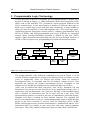
3 Programmable Logic Technology______________________________ 56
3.1
CPLDs and FPGAs ______________________________________________________ 59
3.2
Altera MAX 7000S Architecture – A Product Term CPLD Device _______________ 60
Rapid Prototyping of Digital Systems
vi
3.3
Altera Cyclone Architecture – A Look-Up Table FPGA Device _________________ 62
3.4
Xilinx 4000 Architecture – A Look-Up Table FPGA Device ____________________ 65
3.5
Computer Aided Design Tools for Programmable Logic _______________________ 67
3.6
Next Generation FPGA CAD tools _________________________________________ 68
3.7
Applications of FPGAs ___________________________________________________ 69
3.8
Features of New Generation FPGAs________________________________________ 69
3.9
For additional information _______________________________________________ 70
3.10
Laboratory Exercises ____________________________________________________ 71
4 Tutorial II: Sequential Design and Hierarchy ____________________ 74
4.1
Install the Tutorial Files and FPGAcore Library for your board ________________ 74
4.2
Open the tutor2 Schematic _______________________________________________ 75
4.3
Browse the Hierarchy____________________________________________________ 76
4.4
Using Buses in a Schematic _______________________________________________ 78
4.5
Testing the Pushbutton Counter and Displays _______________________________ 79
4.6
Testing the Initial Design on the Board _____________________________________ 80
4.7
Fixing the Switch Contact Bounce Problem__________________________________ 81
4.8
Testing the Modified Design on the FPGA Board _____________________________ 82
4.9
Laboratory Exercises ____________________________________________________ 83
5 FPGAcore Library Functions _________________________________ 88
5.1
FPGAcore LCD_Display: LCD Panel Character Display ______________________ 90
5.2
FPGAcore DEC_7SEG: Hex to Seven-segment Decoder _______________________ 92
5.3
FPGAcore Debounce: Pushbutton Debounce ________________________________ 94
5.4
FPGAcore OnePulse: Pushbutton Single Pulse ______________________________ 95
5.5
FPGAcore Clk_Div: Clock Divider_________________________________________ 96
5.6
FPGAcore VGA_Sync: VGA Video Sync Generation _________________________ 97
5.7
FPGAcore Char_ROM: Character Generation ROM_________________________ 99
5.8
FPGAcore Keyboard: Read Keyboard Scan Code ___________________________ 100
5.9
FPGAcore Mouse: Mouse Cursor _________________________________________ 102
5.10
For additional information ______________________________________________ 103
6 Using VHDL for Synthesis of Digital Hardware _________________ 106
6.1
VHDL Data Types _____________________________________________________ 106
6.2
VHDL Operators ______________________________________________________ 107
6.3
VHDL Based Synthesis of Digital Hardware ________________________________ 108
6.4
VHDL Synthesis Models of Gate Networks _________________________________ 108
Table of Contents
vii
6.5
VHDL Synthesis Model of a Seven-segment LED Decoder_____________________ 109
6.6
VHDL Synthesis Model of a Multiplexer ___________________________________ 111
6.7
VHDL Synthesis Model of Tri-State Output_________________________________ 112
6.8
VHDL Synthesis Models of Flip-flops and Registers __________________________ 112
6.9
Accidental Synthesis of Inferred Latches ___________________________________ 114
6.10
VHDL Synthesis Model of a Counter ______________________________________ 114
6.11
VHDL Synthesis Model of a State Machine _________________________________ 115
6.12
VHDL Synthesis Model of an ALU with an Adder/Subtractor and a Shifter ______ 117
6.13
VHDL Synthesis of Multiply and Divide Hardware __________________________ 118
6.14
VHDL Synthesis Models for Memory ______________________________________ 119
6.15
Hierarchy in VHDL Synthesis Models _____________________________________ 123
6.16
Using a Testbench for Verification ________________________________________ 125
6.17
For additional information _______________________________________________ 126
6.18
Laboratory Exercises____________________________________________________ 126
7 Using Verilog for Synthesis of Digital Hardware ________________ 130
7.1
Verilog Data Types _____________________________________________________ 130
7.2
Verilog Based Synthesis of Digital Hardware ________________________________ 130
7.3
Verilog Operators ______________________________________________________ 131
7.4
Verilog Synthesis Models of Gate Networks _________________________________ 132
7.5
Verilog Synthesis Model of a Seven-segment LED Decoder ____________________ 132
7.6
Verilog Synthesis Model of a Multiplexer ___________________________________ 133
7.7
Verilog Synthesis Model of Tri-State Output ________________________________ 134
7.8
Verilog Synthesis Models of Flip-flops and Registers _________________________ 135
7.9
Accidental Synthesis of Inferred Latches ___________________________________ 136
7.10
Verilog Synthesis Model of a Counter ______________________________________ 136
7.11
Verilog Synthesis Model of a State Machine_________________________________ 137
7.12
Verilog Synthesis Model of an ALU with an Adder/Subtractor and a Shifter _____ 138
7.13
Verilog Synthesis of Multiply and Divide Hardware __________________________ 139
7.14
Verilog Synthesis Models for Memory _____________________________________ 140
7.15
Hierarchy in Verilog Synthesis Models _____________________________________ 143
7.16
For additional information _______________________________________________ 144
7.17
Laboratory Exercises____________________________________________________ 144
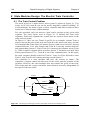
8 State Machine Design: The Electric Train Controller_____________ 148
8.1
The Train Control Problem ______________________________________________ 148
viii
Rapid Prototyping of Digital Systems
8.2
Train Direction Outputs (DA1-DA0, and DB1-DB0) _________________________ 149
8.3
Switch Direction Outputs (SW1, SW2, and SW3) ____________________________ 150
8.4
Train Sensor Input Signals (S1, S2, S3, S4, and S5) __________________________ 150
8.5
An Example Controller Design ___________________________________________ 151
8.6
VHDL Based Example Controller Design __________________________________ 154
8.7
Verilog Based Example Controller Design__________________________________ 157
8.8
Automatically Generating a State Diagram of a Design _______________________ 160
8.9
Simulation Vector file for State Machine Simulation _________________________ 161
8.10
Running the Train Control Simulation ____________________________________ 162
8.11
Running the Video Train System (After Successful Simulation) ________________ 162
8.12
A Hardware Implementation of the Train System Layout_____________________ 164
8.13
Laboratory Exercises ___________________________________________________ 166
9 A Simple Computer Design: The µP 3 _________________________ 170
9.1
Computer Programs and Instructions _____________________________________ 171
9.2
The Processor Fetch, Decode and Execute Cycle_____________________________ 172
9.3
VHDL Model of the μP 3 ________________________________________________ 179
9.4
Verilog Model of the μP 3 _______________________________________________ 182
9.5
Automatically Generating a State Diagram of the μP3________________________ 186
9.6
Simulation of the μP3 Computer__________________________________________ 187
9.7
Laboratory Exercises ___________________________________________________ 188
10 VGA Video Display Generation using FPGAs ___________________ 192
10.1
Video Display Technology _______________________________________________ 192
10.2
Video Refresh _________________________________________________________ 192
10.3
Using an FPGA for VGA Video Signal Generation __________________________ 195
10.4
A VHDL Sync Generation Example: FPGAcore VGA_SYNC _________________ 196
10.5
Final Output Register for Video Signals ___________________________________ 198
10.6
Required Pin Assignments for Video Output _______________________________ 198
10.7
Video Examples________________________________________________________ 199
10.8
A Character Based Video Design _________________________________________ 200
10.9
Character Selection and Fonts ___________________________________________ 200
10.10 VHDL Character Display Design Examples ________________________________ 203
10.11 A Graphics Memory Design Example _____________________________________ 206
10.12 Video Data Compression ________________________________________________ 207
10.13 Video Color Mixing using Dithering_______________________________________ 207
Table of Contents
ix
10.14 VHDL Graphics Display Design Example __________________________________ 208
10.15 Higher Video Resolution and Faster Refresh Rates ___________________________ 209
10.16 Laboratory Exercises____________________________________________________ 210
11 Interfacing to the PS/2 Keyboard and Mouse ___________________ 214
11.1
PS/2 Port Connections___________________________________________________ 214
11.2
Keyboard Scan Codes ___________________________________________________ 215
11.3
Make and Break Codes __________________________________________________ 215
11.4
The PS/2 Serial Data Transmission Protocol ________________________________ 216
11.5
Scan Code Set 2 for the PS/2 Keyboard_____________________________________ 218
11.6
The Keyboard FPGAcore ________________________________________________ 220
11.7
A Design Example Using the Keyboard FPGAcore ___________________________ 223
11.8
Interfacing to the PS/2 Mouse ____________________________________________ 224
11.9
The Mouse FPGAcore ___________________________________________________ 226
11.10 Mouse Initialization _____________________________________________________ 226
11.11 Mouse Data Packet Processing ____________________________________________ 227
11.12 An Example Design Using the Mouse FPGAcore_____________________________ 228
11.13 For Additional Information ______________________________________________ 229
11.14 Laboratory Exercises____________________________________________________ 229
12 Legacy Digital I/O Interfacing Standards ______________________ 232
12.1
Parallel I/O Interface____________________________________________________ 232
12.2
RS-232C Serial I/O Interface _____________________________________________ 233
12.3
SPI Bus Interface _______________________________________________________ 235
12.4
I2C Bus Interface _______________________________________________________ 237
12.5
For Additional Information ______________________________________________ 239
12.6
Laboratory Exercises____________________________________________________ 239
13 FPGA Robotics Projects ____________________________________ 242
13.1
The FPGA-bot Design ___________________________________________________ 242
13.2
FPGA-bot Servo Drive Motors____________________________________________ 242
13.3
Modifying the Servos to make Drive Motors ________________________________ 243
13.4
VHDL Servo Driver Code for the FPGA-bot ________________________________ 244
13.5
Low-cost Sensors for an FPGA Robot Project _______________________________ 246
13.6
Assembly of the FPGA-bot Body __________________________________________ 259
13.7
I/O Connections to the board’s Expansion Headers __________________________ 266
13.8
Robot Projects Based on R/C Toys, Models, and Robot Kits ___________________ 267
Rapid Prototyping of Digital Systems
x
13.9
For Additional Information ______________________________________________ 275
13.10 Laboratory Exercises ___________________________________________________ 277
14 A RISC Design: Synthesis of the MIPS Processor Core ___________ 284
14.1
The MIPS Instruction Set and Processor ___________________________________ 284
14.2
Using VHDL to Synthesize the MIPS Processor Core ________________________ 287
14.3
The Top-Level Module __________________________________________________ 288
14.4
The Control Unit_______________________________________________________ 291
14.5
The Instruction Fetch Stage______________________________________________ 293
14.6
The Decode Stage ______________________________________________________ 296
14.7
The Execute Stage______________________________________________________ 298
14.8
The Data Memory Stage ________________________________________________ 300
14.9
Simulation of the MIPS Design ___________________________________________ 301
14.10 MIPS Hardware Implementation on the FPGA Board _______________________ 302
14.11 For Additional Information ______________________________________________ 303
14.12 Laboratory Exercises ___________________________________________________ 304
15 Introducing System-on-a-Programmable-Chip __________________ 310
15.1
Processor Cores________________________________________________________ 310
15.2
SOPC Design Flow _____________________________________________________ 311
15.3
Initializing Memory ____________________________________________________ 313
15.4
SOPC Design versus Traditional Design Modalities __________________________ 315
15.5
An Example SOPC Design_______________________________________________ 316
15.6
Hardware/Software Design Alternatives ___________________________________ 317
15.7
For additional information ______________________________________________ 317
15.8
Laboratory Exercises ___________________________________________________ 318
16 Tutorial III: Nios II Processor Software Development ____________ 322
16.1
Install the DE board files ________________________________________________ 322
16.2
Starting a Nios II Software Project ________________________________________ 322
16.3
The Nios II IDE Software________________________________________________ 324
16.4
Generating the Nios II System Library ____________________________________ 325
16.5
Software Design with Nios II Peripherals __________________________________ 326
16.6
Starting Software Design – main() ________________________________________ 329
16.7
Downloading the Nios II Hardware and Software Projects ____________________ 330
16.8
Executing the Software__________________________________________________ 331
16.9
Starting Software Design for a Peripheral Test Program _____________________ 331
Table of Contents
xi
16.10 Handling Interrupts_____________________________________________________ 334
16.11 Accessing Parallel I/O Peripherals_________________________________________ 335
16.12 Communicating with the LCD Display (DE2 only) ___________________________ 336
16.13 Testing SRAM _________________________________________________________ 339
16.14 Testing Flash Memory___________________________________________________ 340
16.15 Testing SDRAM ________________________________________________________ 341
16.16 Downloading the Nios II Hardware and Software Projects ____________________ 346
16.17 Executing the Software __________________________________________________ 347
16.18 For additional information _______________________________________________ 347
16.19 Laboratory Exercises____________________________________________________ 348
17 Tutorial IV: Nios II Processor Hardware Design ________________ 352
17.1
Install the DE board files ________________________________________________ 352
17.2
Creating a New Project __________________________________________________ 352
17.3
Starting SOPC Builder __________________________________________________ 353
17.4
Adding a Nios II Processor _______________________________________________ 355
17.5
Adding UART Peripherals _______________________________________________ 358
17.6
Adding an Interval Timer Peripheral ______________________________________ 359
17.7
Adding Parallel I/O Components __________________________________________ 360
17.8
Adding an SRAM Memory Controller _____________________________________ 361
17.9
Adding an SDRAM Memory Controller ____________________________________ 362
17.10 Adding the LCD Module (DE2 Board Only) _________________________________ 362
17.11 Adding an External Bus _________________________________________________ 363
17.12 Adding Components to the External Bus ___________________________________ 364
17.13 Global Processor Settings ________________________________________________ 364
17.14 Finalizing the Nios II Processor ___________________________________________ 365
17.15 Add the Processor Symbol to the Top-Level Schematic _______________________ 366
17.16 Create a Phase-Locked Loop Component___________________________________ 367
17.17 Complete the Top-Level Schematic ________________________________________ 368
17.18 Design Compilation _____________________________________________________ 368
17.19 Testing the Nios II Project _______________________________________________ 369
17.20 For additional information _______________________________________________ 370
17.21 Laboratory Exercises____________________________________________________ 370
18 Operating System Support for SOPC Design ____________________ 374
18.1
Nios II OS Support _____________________________________________________ 376
xii
Rapid Prototyping of Digital Systems
18.2
eCos _________________________________________________________________ 377
18.3
µC/OS-II _____________________________________________________________ 378
18.4
µClinux ______________________________________________________________ 379
18.5
Implementing the µClinux on the DE Board ________________________________ 380
18.6
Hardware Design for µClinux Support ____________________________________ 380
18.7
Configuring the DE Board_______________________________________________ 382
18.8
Exploring µClinux on the DE Board_______________________________________ 385
18.9
PS/2 Device Support in µClinux __________________________________________ 386
18.10 Video Display in µClinux ________________________________________________ 386
18.11 USB Devices in µClinux (DE2 Board Only) _________________________________ 387
18.12 Network Communication in µClinux (DE2 Board Only) ______________________ 387
18.13 For additional information ______________________________________________ 388
18.14 Laboratory Exercises ___________________________________________________ 388
Appendix A: Generation of Pseudo Random Binary Sequences _______ 391
Appendix B: Quartus II Design and Data File Extensions ____________ 393
Appendix C: Common FPGA Pin Assignments _____________________ 394
Appendix D: ASCII Character Code______________________________ 396
Appendix E: Common I/O Connector Pin Assignments ______________ 397
Glossary ____________________________________________________ 399
Index ______________________________________________________ 407
About the Accompanying DVD__________________________________ 411
PREFACE
Changes to the SOPC Edition
Rapid Prototyping of Digital Systems provides an exciting and challenging
laboratory component for undergraduate digital logic and computer design courses
using FPGAs and CAD tools for simulation and hardware implementation. The
more advanced topics and exercises also make this text useful for upper level
courses in digital logic, programmable logic, and embedded systems. The SOPC
edition includes Altera’s new Quartus II CAD tool and includes laboratory projects
for Altera’s DE2 and the new DE1 FPGA boards. Student laboratory projects
provided on the book’s DVD include video graphics and text, mouse and keyboard
input, and several computer designs.
Rapid Prototyping of Digital Systems includes four tutorials on the Altera Quartus
II and Nios II tool environment, an overview of programmable logic, and IP cores
with several easy-to-use input and output functions. These features were developed
to help students get started quickly. Early design examples use schematic capture
and IP cores developed for the Altera UP and DE FPGA boards. VHDL is used for
more complex designs after a short introduction to VHDL-based synthesis. Verilog
is also now supported as an option for the student projects.
New chapters in this edition provide an overview of System-On-a-Programmable
Chip (SOPC) technology and SOPC design examples for the DE1 & 2 boards using
Altera’s new Nios II Processor hardware, the C software development tools, an
overview of OS support for SOPC, and the uClinux operating system. A full set of
Altera’s FPGA CAD tools is included on the book’s DVD.
Intended Audience
This text is intended to provide an exciting and challenging laboratory
component for an undergraduate digital logic design class. The more advanced
topics and exercises are also appropriate for consideration at schools that have
an upper level course in digital logic or programmable logic. There are a
number of excellent texts on digital logic design. For the most part, these texts
do not include or fully integrate modern CAD tools, logic simulation, logic
synthesis using hardware description languages, design hierarchy, current
generation field programmable gate array (FPGA) technology and SOPC
design. The goal of this text is to introduce these topics in the laboratory
portion of the course. Even student laboratory projects can now implement
entire digital and computer systems with hundreds of thousands of gates.
Over the past eight years, we have developed a number of interesting and
challenging laboratory projects involving serial communications, state
machines with video output, video games and graphics, simple computers,
keyboard and mouse interfaces, robotics, and pipelined RISC processor cores.
xiv
Rapid Prototyping of Digital Systems
Source files and additional example files are available on the DVD for all
designs presented in the text. The student version of the PC based CAD tool on
the DVD can be freely distributed to students. Students can purchase their own
FPGA board for little more than the price of a contemporary textbook. As an
alternative, a few of the low-cost FPGA boards can be shared among students
in a laboratory. Course instructors should contact the Altera University Program
for detailed information on obtaining full versions of the CAD tools for
laboratory PCs and educational FPGA boards for student laboratories.
Topic Selection and Organization
Chapter 1 is a short CAD tool tutorial that covers design entry, simulation, and
hardware implementation using an FPGA. The majority of students can enter
the design, simulate, and have the design successfully running on the FPGA
board in less than thirty minutes. After working through the tutorial and
becoming familiar with the process, similar designs can be accomplished in less
than 10 minutes.
Chapter 2 provides an overview of the various FPGA development boards. The
features of each board are briefly described. Several tables listing pin
connections of various I/O devices serve as an essential reference whenever a
hardware design is implemented on the DE1, DE2, UP3, or UP 2 FPGA boards.
Chapter 3 is an introduction to programmable logic technology. The
capabilities and internal architectures of the most popular CPLDs and FPGAs
are described. These include the Cyclone FPGA used on the FPGA board, and
the Xilinx 4000 family FPGAs.
Chapter 4 is a short CAD tool tutorial that serves as both a hierarchical and
sequential design example. A counter is clocked by a pushbutton and the output
is displayed in the seven-segment LEDs. The design is downloaded to the
FPGA board and some real world timing issues arising from switch contact
bounce are resolved. It uses several functions from the FPGAcore library which
greatly simplify use of the FPGA’s input and output capabilities.
Chapter 5 describes the available FPGAcore library I/O functions. The I/O
devices include switches, the LCD, a decoder for seven segment LEDs, a
multiple output clock divider, VGA output, keyboard input, and mouse input.
Chapter 6 is an introduction to the use of VHDL for the synthesis of digital
hardware. Rather than a lengthy description of syntax details, models of the
commonly used digital hardware devices are developed and presented. Most
VHDL textbooks use models developed only for simulation and frequently use
language features not supported in synthesis tools. Our easy to understand
synthesis examples were developed and tested on FPGAs using the Altera CAD
tools.
Chapter 7 is an introduction to the use of Verilog for the synthesis of digital
hardware. The same hardware designs as Chapter 6 as modeled in Verilog. It is
optional, but is included for those who would like an introduction to Verilog.
Chapter 8 is a state machine design example. The state machine controls a
virtual electric train simulation with video output generated directly by the
FPGA. Using track sensor input, students must control two trains and three
Preface
xv
track switches to avoid collisions. An actual model train layout can also built
using the new digital DCC trains interfaced to an FPGA board.
Chapter 9 develops a model of a simple computer. The fetch, decode, and
execute cycle is introduced and a brief model of the computer is developed
using VHDL. A short assembly language program can be entered in the FPGA’s
internal memory and executed in the simulator.
Chapter 10 describes how to design an FPGA-based digital system to output
VGA video. Numerous design examples are presented containing video with
both text and graphics. Fundamental design issues in writing simple video
games and graphics using an FPGA board are examined.
Chapter 11 describes the PS/2 keyboard and mouse operation and presents
interface examples for integrating designs on an FPGA board. Keyboard scan
code tables, mouse data packets, commands, status codes, and the serial
communications protocol are included. VHDL code for a keyboard and mouse
interface is also presented.
Chapter 12 describes several of the common I/O standards that are likely to be
encountered in FPGA systems. Parallel, RS232 serial, SPI, and I2C standards
and interfacing are discussed.
Chapter 13 develops a design for an adaptable mobile robot using an FPGA
board as the controller. Servo motors and several sensor technologies for a low
cost mobile robot are described. A sample servo driver design is presented.
Commercially available parts to construct the robot described can be obtained
for as little as $60. Several robots can be built for use in the laboratory.
Students with their own FPGA board may choose to build their own robot
following the detailed instructions found in section 13.6.
Chapter 14 describes a single clock cycle model of the MIPS RISC processor
based on the hardware implementation presented in the widely used Patterson
and Hennessy textbook, Computer Organization and Design the
Hardware/Software Interface. Laboratory exercises that add new instructions,
features, and pipelining are included at the end of the chapter.
Chapters 15, 16, and 17 introduce students to SOPC design using the Nios II
RISC processor core. Chapter 15 is an overview of the SOPC design approach.
Chapter 16 contains a tutorial for the Nios II IDE software development tool
and examples using the Nios II C/C++ compiler. Chapter 17 contains a tutorial
on the processor core hardware configuration tool, SOPC builder. A DE2, DE1,
or FPGA board is required for this new material since it is not supported on the
UP2 or UP1’s smaller FPGA.
Chapter 18 is new to the fourth edition and introduces students to a Linux
based Real-Time Operating System (RTOS). A tutorial shows how the Clinux
OS can be ported to the DE2 and DE1 FPGA boards.
We anticipate that some schools will still choose to begin with TTL designs on
a small protoboard for the first few labs. The first chapter can be started at this
time since only OR and NOT logic functions are used to introduce the CAD
tool environment. The CAD tool can also be used for simulation of TTL labs,
since a TTL parts library is included.
xvi
Rapid Prototyping of Digital Systems
Even though VHDL and Verilog are complex languages, we have found after
several years of experimentation that students can write HDL models to
synthesize hardware designs after a short overview with a few basic hardware
design examples. The use of HDL templates and online help files in the CAD
tool make this process easier. After the initial experience with HDL synthesis,
students dislike the use of schematic capture on larger designs since it can be
time consuming. Experience in industry has been much the same since large
productivity gains have been achieved using HDL based synthesis tools for
FPGAs and Application Specific Integrated Circuits (ASICs).
Most digital logic classes include a simple computer design such as the one
presented in Chapter 9 or a RISC processor such as the one presented in
Chapter 14. If this is not covered in the first digital logic course, it could be
used as a lab component for a subsequent computer architecture class.
A typical quarter or semester length course could not cover all of the topics
presented. The material in Chapters 7 through 17 can be used on a selective
basis. The keyboard and mouse are supported by FPGAcore library functions,
and the material presented in Chapter 11 is not required to use these library
functions for keyboard or mouse input. A DE1, DE2, or FPGA board is required
for the SOPC Nios designs in Chapters 16 and 17.
A video game based on the material in Chapter 10 can serve as the basis for a
final design project. We use robots with sensors from Chapter 13 that are
controlled by the simple computer in Chapter 9. Students really enjoy working
with the robot, and it presents almost infinite possibilities for an exciting design
competition. More advanced classes might want to develop projects based on
the Nios II processor reference design in Chapter 16 and 17 using C/C++ code
or use the uClinux material in Chapter 18 to develop more complex application
programs for embedded devices.
Software and Hardware Packages
We recommend the use of the new 7.1 SP1 web version of Quartus II FPGA
CAD included with this book; all exercises were tested using this version.
FPGA boards are available from the Altera University Program at special
student pricing. Although boards can be easily shared among several students in
a lab setting, pricing makes it possible for students who would like to purchase
their own to do so.
Details and suggestions for additional cables that may be required for a
laboratory setup can be found in Section 2.4. Source files for all designs
presented in the text are available on the DVD.
Additional Web Material and Resources
There is a web site for the text with additional course materials, slides, text
errata, and software updates at:
http://www.ece.gatech.edu/users/hamblen/book/book4e.htm
Preface
xvii
Acknowledgments
Over three thousand students and several hundred teaching assistants have
contributed to this work during the past eight years. In particular, we would like
to acknowledge Doug McAlister, Michael Sugg, Jurgen Vogel, Greg Ruhl, Eric
Van Heest, Mitch Kispet, Evan Anderson, Zachary Folkerts, and Nick Clark for
their help in testing and developing several of the laboratory assignments and
tools. Stephen Brown, Mike Phipps, Joe Hanson, Tawfiq Mossadak, and Eric
Shiflet at Altera provided software, hardware, helpful advice, and
encouragement.
CHAPTER 1
Tutorial I:
The 15-Minute Design
2
Rapid Prototyping of Digital Systems
Chapter 1
1 Tutorial I: The 15 Minute Design
The purpose of this tutorial is to introduce the user to the Altera CAD tools and
the University Program (DE1, DE2, UP3, UP2, or UP1) FPGA Development
Boards in the shortest possible time. The format is an aggressive introduction to
schematic, VHDL, and Verilog entry for those who want to get started quickly.
The approach is tutorial and utilizes a path that is similar to most digital design
processes.
Once you have completed this tutorial, you will understand and be able to:
•
•
•
•
•
Navigate the Altera schematic entry environment,
Compile a VHDL or Verilog design file,
Simulate, debug, and test your designs,
Generate and verify timing characteristics, and
Download and run your design on a DE1, DE2, UP3, UP2, or UP1
board.
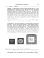
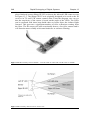
Determining your FPGA Board Type
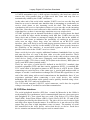
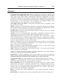
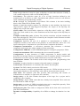
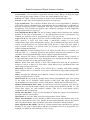
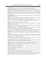
The first step is to identify which one of the various Altera Educational FPGA
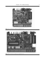
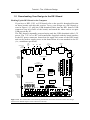
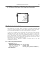
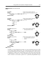
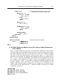
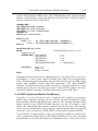
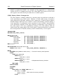
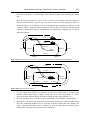
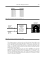
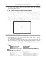
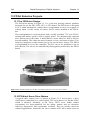
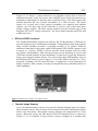
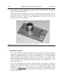
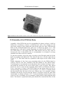
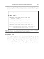
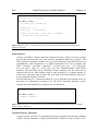
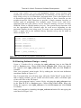
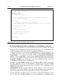
boards you are using for the tutorial. Examine the photographs in Figures 1.1
to 1.4 and compare them to your board to determine which type of board you
are using.
There will be some minor variations in the instructions later on that depend on
which board type you are using. After identifying your board, be sure to
remember which model of Altera FPGA board you have (i.e., DE1, DE2, UP3,
UP2 or UP1).
If your board looks like Figure 1.4 and you see UP1X printed on the board,
some early UP2 production boards had the designation UP1X printed on the
board. The UP1X is electronically equivalent to a UP2 board and contains the
same FPGA, so follow the instructions for a UP2 board.
If you have a UP3 board, the UP3 board comes in two versions and you need
to determine which version you have. The 1C12 version contains a larger
EP1C12 FPGA instead of the EP1C6 FPGA. Check the part number on the
FPGA chip on the left center of the board.
Tutorial I: The 15-Minute Design
Figure 1.1 The Altera DE1 FPGA Development board.
Figure 1.2 The Altera DE2 FPGA Development board.
3
4
Rapid Prototyping of Digital Systems
Chapter 1
Figure 1.3 The Altera UP3 FPGA Development board. The 1C12 version has a larger EP1C12Q240
FPGA. (Check the part number on the large square FPGA chip in middle of board).
Figure 1.4 The Altera UP2 FPGA development board. UP1 boards appear very similar and can also
be used, but instead of a FLEX EPF10K70 they use a smaller EPF10K20 FPGA that contains fewer
logic elements. (Check the part number on the large square FPGA chip on right side of your board)
Tutorial I: The 15-Minute Design
5
In this tutorial, a simple OR logic function will be demonstrated to provide an
introduction to the Altera Quartus II CAD tools. After simulation, the design
will then be used to program a field programmable gate array (FPGA) on an
FPGA development board. The design will then be tested running on real
hardware.
ALTERA’S NEWEST BOARDS ARE THE DE1 AND DE2. IF YOU HAVE ONE OF THE OTHER FPGA
BOARDS AS SEEN IN FIGURES 1.1 TO 1.4, YOU SHOULD ALWAYS FOLLOW THE INSTRUCTIONS
AND PROCEDURES OUTLINED IN THE TEXT AND ON THE DVD FOR YOUR BOARD. THE DVD
CONTAINS ADDITIONAL INFORMATION AND FILES FOR THE OLDER FPGA BOARDS.
The inputs to the OR logic will be two pushbuttons and the output will be
displayed using a light emitting diode (LED). Both the pushbuttons and the
LED are part of the development board, and no external wiring is required.
Of course, any actual design will be more complex, but the objective here is to
quickly understand the capabilities and flow of the design tools with minimal
effort and time.
More complex digital designs including computers and color video graphics
will be introduced later in this text after you have become familiar with the
development tools and hardware description languages (Hals) used in digital
designs.
Granted, all this may not be accomplished in just 15 minutes; however, the
skills acquired from this demonstration tutorial will enable the first-time user
to duplicate similar designs in less time than that!
INSTALL THE QUARTUS II WEB VERSION SOFTWARE USING THE DVD AND OBTAIN A WEB
LICENSE FILE FROM ALTERA. CHECK FOR ALTERA QUARTUS II W EB VERSION SOFTWARE
UPDATES AT WWW.ALTERA.COM. THE BOOKS DESIGNS WERE ALL TESTED WITH VERSION 7.1
SP1. AS NEWER VERSIONS OF THE ALTERA SOFTWARE APPEAR, MINOR CHANGES MAY BE
NEEDED. CHECK THE BOOK’ S WEBSITE FOR ANY UPDATES .
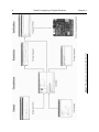
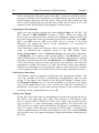
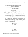
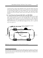
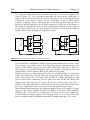
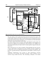
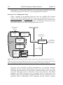
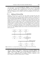
With the standard FPGA computer aided design tools, designs can be entered
via schematic capture or by using a Hardware Description Language (HDL)
such as VHDL or Verilog. It is also possible to combine blocks with different
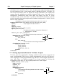
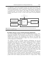
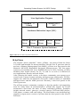
entry methods into a single design. As seen in Figure 1.5, tools can then be
used to simulate, calculate timing delays, synthesize logic, and program a
hardware implementation of the design on an FPGA.
Rapid Prototyping of Digital Systems
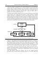
Figure 1.5 Design process for schematic or HDL entry.
6
Chapter 1
Tutorial I: The 15-Minute Design
7
The Board
The default boards that will be used are the newer DE1 and DE2 boards.
Although the following tutorial can be done with any of the DE1, DE2, UP3,
UP2 or UP1 boards. Some minor modifications (i.e., the FPGA device number
and pin number assignments) will be needed for the other boards. In this
tutorial, complete instructions will be provided for all of the different FPGA
boards.
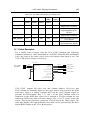
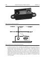
The Pushbuttons
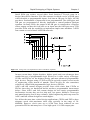
On the FPGA board, two pushbutton switch inputs, PB1 and PB2, are
connected to FPGA input pins. Each pushbutton input is tied “High” with a
pull-up resistor and pulled “Low” when the respective pushbutton is pressed.
One needs to remember that when using the on-board pushbuttons, this "active
low" condition ties zero volts to the input when the button is pressed and the
Vcc high supply to the input when not pressed. See Figure 1.6. Vcc is 3.3V on
newer boards and 5V on the older UP2 and 1 boards. On the FPGA board
shown on the left in Figure 1.6, a logic “0” at the output turns on the LED.
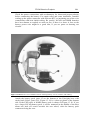
Figure 1.6 FPGA I/O connections to Pushbuttons (PBx) and LED: Right of center, active LOW LED
output (i.e., UP1 and UP2 boards) or on far right active HIGH LED output (i.e., DE1, DE2, and UP3
boards). Note that a depressed pushbutton input will be LOW.
The LED Outputs
On many of the newer FPGA development boards including the DE1 and DE2,
the LED is connected with active HIGH outputs as in the right LED output
illustration in Figure 1.6. This allows a HIGH signal on the output pin of the
FPGA to turn the LED on and a LOW signal to turn it off.
Historically, most digital logic output pins were designed to sink more current
than they could source. In such cases, it makes sense to let the output pin of
the FPGA tie the cathode (-) of the LED to ground to allow for a brighter LED
(i.e., more current flowing); however, this configuration has the side effect of
requiring a LOW signal to turn the LED on, but is generally the more common
8
Rapid Prototyping of Digital Systems
Chapter 1
configuration. This active LOW output is actually the arrangement used on all
seven segment LED displays on all of the FPGA development boards.
The Problem Definition
To illustrate the capabilities of the software in the simplest terms, we will
build a circuit that turns off the LED when one OR the other pushbutton is
pushed. In a simple logic equation, one could write:
LED_OFF = PB1_HIT + PB2_HIT
At first, this may seem too simple; however, the active low inputs and outputs
add just enough complication to illustrate some of the more common errors,
and it provides an opportunity to compare some of the different syntax features
of VHDL and Verilog. (Students needing an exercise in DeMorgan's Law will
also find these exercises particularly enlightening.)
We will first build this circuit with the graphical editor and then implement it
in VHDL and Verilog. As you work through the tutorial, note how the design
entry method is relatively independent of the compile, timing, and simulation
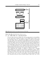
steps, and which FPGA board is used for the hardware implementation.
Resolving the Active Low Signals
Since the pushbuttons generate inverted signals and the LED requires an
inverted or low level logic signal to turn off, we could build an OR logic
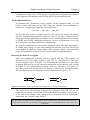
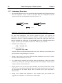
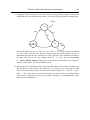
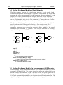
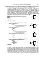
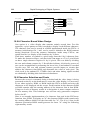
circuit using the layout in Figure 1.7a. Recalling that a bubble on a gate input
or output indicates inversion, careful examination shows that the two circuits
in Figure 1.7 are functionally equivalent; however, the circuit in Figure 1.7a
uses more gates and would take a bit longer to enter in the schematic editor.
We will therefore use the single gate circuit illustrated in Figure 1.7b.
(a)
(b)
Figure 1.7a and 1.7b. Equivalent circuits for ORing active low inputs and outputs.
This form of the OR function is known as a "negative-logic OR." If you are
confused, try writing a truth table to show this Boolean equality. (In Exercise 1
at the end of the chapter, this circuit will be compared with its DeMorgan’s
equivalent, the "positive-logic AND.").
ON THE UP2 AND UP1 BOARDS, THE LEDS OUTPUT STATE WILL APPEAR INVERTED SINCE ITS
LED OUTPUT CIRCUIT IS INVERTED, SO PUSHING ONE OF THE PUSHBUTTONS WILL TURN ON
THE LED.
Tutorial I: The 15-Minute Design
9
1.1 Design Entry using the Graphic Editor
Examine the CAD tool overview diagram in Figure 1.5. The initial path in this
section will be from schematic capture (Graphical Entry) to downloading the
design to the FPGA board. On the way, we will pass through some of the
nuances of the Compiler along with setting up and controlling a simulation.
Later, after having actually tested the design, we will examine the Timing
Analysis information of the design. Although relatively short, each step is
carefully illustrated and explained. Install the Altera Quartus II software on
your PC using the book’s DVD, if it is not already installed.
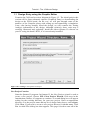
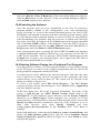
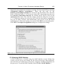
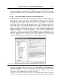
Figure 1.8 Creating a new Quartus II Project.
New Project Creation
Start the Quartus II program. In Quartus II, the New Project wizard is used to
create a new project. Choose File New Project Wizard. Click next in the
Introduction window, if it appears to continue. A second dialog box will appear
asking for the working directory for your new project. Enter an appropriate
directory. For the project name and top-level design entity boxes, enter orgate.
Click Next. If you need to create a new project directory with that name, click
Yes. An Add Files dialog box then appears. This page is used to enter all of the
10
Rapid Prototyping of Digital Systems
Chapter 1
design files (other than the top-level file). Since this simple project will only
use a single top-level design file, click Next.
Select the FPGA Device to be Used
The next dialog box is used to select the FPGA device type as seen in Figure
1.9. The detailed instructions for this step will vary depending on your board
type.
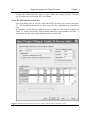
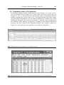
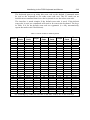
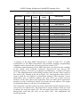
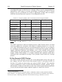
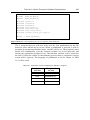
A summary of the different FPGA devices found on each board is shown in
Table 1.1. Find your board’s FPGA family and device part number in Table 1.1
and follow the specific instructions below for your board.
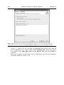
Figure 1.9 Setting the FPGA Device Type. Settings shown are for the DE1 board.
Tutorial I: The 15-Minute Design
11
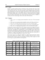
Table 1.1 FPGA Devices used on the various Altera Educational FPGA boards.
FPGA
Family
FPGA
Device
DE1
Cyclone II
DE2
Cyclone II
UP3
Cyclone
UP2 & UP1
FLEX10K
EP2C20F484C7
EP2C35F672C6
EP1C6Q240C8
or 1C12 version
EP1C12Q240C8
EPF10K70RC240-4
or on older UP1s
EPF10K20RV240-4
If you are using a DE1 or DE2 board:
Select the Cyclone II Family FPGA. The DE1 uses an EP2C20F484C7 device
and the DE2 uses a EP2C35F672C6 device.
If you are using the UP3 board:
Select Cyclone family. You will then need to select the specific FPGA device
number on your board. The UP3 is available with two different sizes of
Cyclone FPGAs: an EP1C6Q240C8 (UP3 1C6 board) or the larger
EP1C12Q240C8 (UP3 1C12 board). Check the large square chip in the middle
of the board to verify the exact FPGA part number.
If you are using a UP2 or UP1:
Select FLEX10K family. On the UP2, it will be a EPF10K70RC240-X (-X is
the speed grade of the chip). Check the large square chip in the middle on the
right side of the board to verify the FPGA part number. If you see
EPF10K20RC240 on the FPGA, you have a UP1 board. The original UP1
boards can also be used. The UP1 looks very similar to a UP2 and they use the
same pin assignments and have the same I/O features as the UP2, but they
contain a EPF10K20RC240 FPGA with fewer logic elements. UP1 users
should always follow the instructions for the UP2, but specify the
EPF10K20RC240 device type for each project.
All Boards:
The last digit in the FPGA part number is the speed grade. The correct speed
grade is needed for accurate delays in timing simulations. You may need to
change the setting of the Speed Grade on Pin Count dialog box to Any to
display your specific device. Always choose the correct speed grade to match
your board’s FPGA so that the correct delay times are used in the logic
simulation tools.
If you choose the wrong device type, you will have errors when you attempt to
download your design to the FPGA.
After selecting the correct FPGA part number, click Next, then on the thirdparty EDA tools settings box also click Next since we will not be using any
third-party EDA tools – only Quartus II. Double check the information
summary page that appears and click Finish. In case of problems, use the back
option to make changes.
12
Rapid Prototyping of Digital Systems
Chapter 1
Establishing Graphics (Schematic) as the Input Format
You have now named your project and setup which FPGA will be used, now
choose File New, and a popup menu will appear. Select Block
Diagram/Schematic File, then click OK. This will create a blank schematic
worksheet – a graphics display file (*.gdf file). Note that the toolbar options in
Quartus II are context sensitive and change as different tools are selected. An
empty schematic window with grids will appear named Block1.bdf.
Enter and Place the OR Symbol in Your Schematic
Click on the AND gate icon
on the left-side toolbar. This selects the symbol
tool. In the upper left box under Libraries, expand the library path to see the
options. Find the library named primitives and click on it to expand it. Then
click to expand the logic library. Scroll down the list of logic symbols and
select BNOR2. An OR gate with inverted inputs and outputs should appear in
the symbol window. (The naming convention is B-bubbled NOR with 2 inputs.
Although considered to be a NOR with active low inputs, it is fundamentally
an OR gate with active low inputs and output.) Click OK at the bottom of the
Symbol window.
Figure 1.10 Creating the top-level project schematic design file.
Select the Block1.bdf window and the BNOR2 symbol will appear
in the schematic. Drag the symbol to the middle of the window and
left click to place it. Click on the arrow icon
on the left side
toolbar or hit escape to stop inserting the symbol.
BNOR2
inst
Tutorial I: The 15-Minute Design
13
TO USE THE ONLINE HELP SYSTEM, CLICK HELP ON THE TOP MENU, SELECT SEARCH AND
THEN ENTER BNOR. AT ANY POINT IN THE TUTORIAL , EXTENSIVE ONLINE HELP IS ALWAYS
AVAILABLE . TO SEARCH BY TOPIC OR KEYWORD SELECT THE HELP MENU AND FOLLOW THE
INSTRUCTIONS THERE .
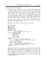
Assigning the Output Pin for Your Schematic
OUTPUT
pin_name
Select the AND gate symbol again on the left side toolbar, expand the pin
library, select output, and click OK. Using the mouse and the left mouse
button, drag the output symbol to the right of the BNOR2 symbol leaving
space between them – they will be connected later.
Figure 1.11 Selecting a new symbol with the Symbol Tool.
Assigning the Input Pins for Your Schematic
pin_name1
INPUT
VCC
Find and place two pin input symbols to the left of the BNOR2 symbol in the
same way that you just selected and placed the output symbol. (Another hint:
Once selected, a symbol can be copied with Right Click Copy and pasted
multiple times using the Right Click Paste function.). Hit the arrow symbol
on the left tool bar and deselect the new symbol by moving the cursor away
and clicking the left mouse button a second time.
14
Rapid Prototyping of Digital Systems
Chapter 1
Connecting the Signal Lines
When you move the mouse cursor near a wire, the cursor changes into a
crosshair. Move to one end of a wire you need to add and push and hold down
the left mouse button. Hold down the left mouse button and drag the end of the
wire to the other point that you want to connect. Release the left button to
connect the wire. If you need to delete a wire, click on it – the wire should turn
blue when selected. Hit the delete key to remove it. You can also use the Right
Click Delete function. Connect the other wires using the same process so
that the diagram looks something like Figure 1.12
Figure 1.12 Active low OR-gate schematic example with I/O pins connected.
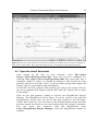
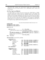
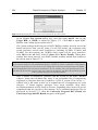
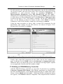
Enter the PIN Names
Right click on the first
INPUT symbol. It will be outlined in blue
and a menu will appear. Select Properties, type PB1 for the pin name and
click OK. Name the other input pin PB2 and the output pin for the LED in a
similar fashion.
Assign the PIN Numbers to Connect the Pushbuttons and the LED
Since the FPGA chip is already prewired to the pushbuttons and the LED on
the printed circuit board (PCB), you need to look up the correct pin numbers
and designate them in your design.
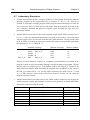
Table 1.2 Hardwired I/O connections on the various FPGA boards in the design example.
I/O Device
DE1 Pin
DE2 Pin
UP3 Pin
UP2 & 1 Pin
PB1
R21 (Key1)
N23 (Key1)
62 (SW7)
28 (FLEX PB1)
PB2
T22 (Key2)
P23 (Key2)
48 (SW4)
29 (FLEX PB2)
LED
R20(LEDR0)
AE23(LEDR0)
56 (D3)
14 (7Seg Dec. pt.)
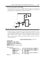
The information in Table 1.2 is from the documentation on the pinouts for the
various FPGA board user’s manuals. (Table 2.4 lists additional I/O pins) In the
Tutorial I: The 15-Minute Design
15
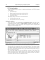
main menu, select Assignments Pin. (If the option to select the pin is
unavailable, you need to go back and select Assignments Device, and make
sure that your device is selected correctly.) You may need to adjust the
Window sizes to find the pin assignment area or select the pulldown,
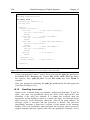
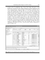
View All Pins List; Figure 1.13 shows the pin list area with pin information
entered. In the “Node Name” column, type the name of the new pin, PB1. In
the “Location” column, double click, scroll down, and select the pin number
for PB1 on your board or type in the pin number in the blank space provided
(NOTE: pin numbers will be different on the various FPGA boards refer to
Table 1.2). The software adds PIN_ to the pin number. Repeat this process
assigning PB2 and LED to the correct pins for your board. After assigning all
three pins and verifying your entries, click File Save Project to save.
Device and pin information is stored in the project’s *.qsf file. Pin names are
also case sensitive.
CAUTION: BE SURE TO USE UNIQUE NAMES FOR DIFFERENT PINS. PINS AND WIRES WITH THE
SAME NAME ARE AUTOMATICALLY CONNECTED EVEN WITHOUT A VISIBLE WIRE SHOWING UP
ON THE SCHEMATIC DIAGRAM.
Figure 1.13 Assigning Pins with the Assignment Editor.
Saving Your Schematic
If you haven’t saved your file yet, Select File Save As and save your project
using the filename ORGATE. Throughout the remainder of this tutorial you
should always refer to the same project directory path when saving or opening
files. A number of other files are automatically created by the Quartus II tools
and maintained in your project directory.
16
Rapid Prototyping of Digital Systems
Chapter 1
Set Unused Pins as Inputs
The memory chips on the development board could all be turned on at the
same time by unused pins on the FPGA, causing their tri-state output drivers to
try to force output data bus bits to different states. This causes high currents,
which can overheat and damage devices after several minutes. To eliminate the
possibility of any damage to the board, the following option should always be
set in a new project. On the menu bar, select Assignments Device then click
the Device and Pin Options button. Click on the Unused Pins tab and check
the As inputs, tri-stated option. Click OK and then OK in the first window.
This setting is saved in the projects *.qsf file. Any time you create a new
project repeat this step.
1.2 Compiling the Design
Compiling your design checks for syntax errors, synthesizes the logic design,
produces timing information for simulation, fits the design on the selected
FPGA, and generates the file required to download the program. After any
changes are made to the design files or pin assignments, the project will
always need to be re-compiled prior to simulation or downloading.
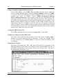
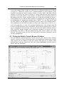
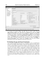
Compiling your Project
Compile by selecting Processing Start Compilation. The compilation
report window will appear in the Quartus II screen and can be used to monitor
the compilation process, view warnings, and errors.
Checking for Compile Warnings and Errors
The project should compile with 0 Errors. If a popup window appears that
states, "Full Compilation was Successful," then you have not made an error.
Info messages will appear in green in the message window. Warnings appear in
blue in the message window and Errors will be red. Errors must be corrected.
If you forget to assign pins, the compiler will select pins based on the best
performance for internal timing and routing. Since the pins for the pushbuttons
and the LED are pre-wired on the FPGA boards, their assignment cannot be
left up to the compiler and the user must always specify them.
Examining the Report File
After compilation, the compiler window shows a summary of the compiled
design including the FPGA logic and memory resources used by the design.
Select the orgate.bdf schematic window. Use View Show Location
Assignments and check the schematic’s I/O pins to verify the correct pin
numbers have been assigned. If a pin is not assigned you may have a typo
somewhere in one of the pin names or you did not save your pin assignments
earlier. You will need to recompile whenever you change pin assignments.
You can also check all of the FPGA’s pins by going to the compiler report
window with Processing Compilation Report, expanding the Fitter file
folder, and clicking on the Pin-out file.
Tutorial I: The 15-Minute Design
17
1.3 Simulation of the Design
For complex designs, the project is normally simulated prior to downloading to
a FPGA. Although the OR example is straightforward, we will take you
through the steps to illustrate the simulation of the circuit.
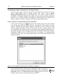
Set Up the Simulation Traces
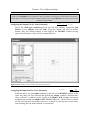
Choose File New, select the Other Files tab, and then from the popup
window select Vector Waveform File and click OK. A blank waveform
window should be displayed. Right click on the Name column on the left side.
Select Insert Nodes or Bus. Click on the Node Finder and then the LIST
button. PB1, PB2 and LED should appear as trace values in the window. Then
click on the center >> button and click OK and OK again. The signals should
appear in the waveform window.
Generate Test Vectors for Simulation
A simulation requires external input data or "stimulus" data to test the circuit.
Since the PB1 and PB2 input signals have not been set to a value, the
simulator sets them to a default of zero. The ‘X’ on the LED trace indicates
that the simulator has not yet been run. (If the simulator has been run and you
still get an ‘X,’ then the simulator was unable to determine the output
condition.)
Right click on PB1; the PB1 trace will be highlighted. Select Value Count
Value, then click on the Timing tab and change the entry in the field
Multiplied By from 1 to 5 and click OK. An alternating pattern of Highs and
Lows should appear in the PB1 trace. (Use View Zoom Out, if you cannot
see the pattern.) Repeat the procedure for PB2 but this time change the entry in
Multiplied By from 1 to 10. PB2 should now be an alternating pattern of ones
and zeros but at twice the frequency of PB1.
(Other useful options in the Value menu will generate a clock and set a signal
High or Low. It is also possible to highlight a portion of a signal trace with the
mouse and set the level manually.)
When you need a longer simulation time in a waveform, you can change the
default simulation end time using Edit End Time.
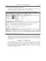
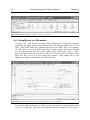
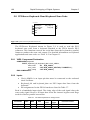
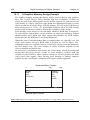
Performing the Simulation with Your Timing Diagram
Select File Save and click the Save button to save your project’s vector
waveform file. Select Processing Start Simulation and click OK on the
window that appears. The simulation should run and the output waveform for
LED should now appear in the Simulation Report window. You may want to
right click on the timing display and use the Zoom options to adjust the time
scale as seen in Figure 1.14.
18
Rapid Prototyping of Digital Systems
Chapter 1
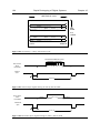
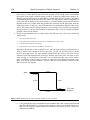
Figure 1.14 Active low OR-gate timing simulation with device time delays.
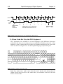
Note that the simulation includes the signal propagation timing delays through
the FPGA and that it takes almost 10 ns (ns = 10-9 sec.) for an input change to
be reflected in the delayed output. Taking this LED output time delay into
account, examine the Simulation Waveform to verify that the LED output is
Low only when either PB1 OR PB2 inputs are Low.
1.4 Testing Your Design on an FPGA Board
The next step is to download the design to a board and test it on real hardware.
At this point, the instructions vary depending on which type of board you are
using for the tutorial. If you do not know your board type, refer back to
Figures 1.1 to 1.4 to identify it. You will need to skip ahead to the appropriate
section for each board as listed below:
•
•
•
•
DE1 users go to Section 1.5 (next Section),
DE2 users skip ahead to Section 1.6,
UP3 users skip ahead to Section 1.7,
UP2 & UP1 users skip ahead to Section 1.8.
Tutorial I: The 15-Minute Design
19
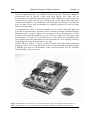
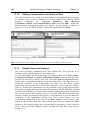
1.5 Downloading Your Design to the DE1 Board
Hooking Up the DE1 Board to the Computer
If you have a DE2, UP2, or UP3 board refer to the specific download Section
on those boards and skip this section. To try your design on a DE1 board as
seen in Figure 1.15, plug the USB download cable into the DE1 board’s USB
connector (top left corner of the board) and attach the other end to an open
USB port on the PC.
The DE1 board is normally powered using only the USB download cable’s 5V
power. The 7.5V AC to DC wall transformer supplied with the board attaches
to the DC power connector located on the upper left corner of the DE2 board
and can be used to supply power to the board when it is not attached to the PC
(i.e., standalone operation).
7.5V DC Power
Supply
Connector
USB
Blaster
Port
Mic
In
Line
In
Line
Out
VGA
Video Port
RS-232
Port
PS/2 Port
Power
ON/OFF
Switch
24-bit Audio CODEC
Ocillators
27Mhz 50MHz 24Mhz
Altera USB
Blaster
Controller
Chipset
Altera EPCS 16
Configuration Device
RUN/PROG
Switch for
JTAG/AS
Modes
90nm
Cyclone II
FPGA with
20K LEs
8MB SDRAM
512KB SRAM
SD Card Socket
4MB Flash
Memory
7-SEG Display Module
10 Red LEDs
8 Green LEDs
SMA
External
Clock
4 Push-button Switches
10 Toggle Switches
Figure 1.15 The Altera DE1 board showing Pushbutton and LED locations used in the design
(enclosed in dashed ellipses seen at bottom of board).
20
Rapid Prototyping of Digital Systems
Chapter 1
After attaching the USB cable, press in the DE1’s red power switch located on
the upper left edge of the board below the USB connector to turn on the board.
When properly powered, the blue power LED on the DE1 board near the
power switch should light up and the other LEDs will all flash, if it is still
setup to run the default demo design shipped from the factory.
Preparing for Downloading
Make sure that you have assigned the correct Device Name for the DE1. The
DE1 contains a EP2C20F484C7 Cyclone II FGPA. When you change the
device type you will also need to redo the pin assignments. Make sure that you
have also assigned the correct pin numbers for the DE1 board. PB1 is pin R22,
PB2 is pin R21 and the LED is pin U22. (refer to section 1.1 for help)
Whenever you change the Device or pin assignments, it is necessary to
recompile before downloading.
After checking to make sure that the cables are hooked up properly, you are
ready to download the compiled circuit to the DE1 board. Select
Tools Programmer. Click on Hardware Setup, select the proper hardware,
a USB-Blaster. (If a window comes up that displays, "No Hardware" to the
right of the Hardware Setup button, use the Hardware Setup button to change
currently selected hardware from "No Hardware" to "USB-Blaster". If a red
JTAG error message appears or the start button is not working, close down the
Programmer window and reopen it. If this still doesn’t correct the problem,
then there is something else wrong with the setup or cable connection. Go back
to the beginning of this section and check each step and connection carefully.)
Final Steps to Download
The filename orgate.sof should be displayed in the programmer window. The
*.sof file contains the FPGA’s configuration (programming) data for your
design. To the right of the filename in the Program/Configure column, check
the Program/Configure box. To start downloading your design to the board,
click on the Start button. Just a few seconds are required to download. If
download is successful, a green info message displays in the system window
notifying you the programming was successful.
Testing Your Design
On the DE1 board, the right two pushbuttons are used in the design and one of
the LEDs to the right just above them. The locations of PB1 (Key0), PB2
(Key1), and the LED (LEDG0) are in the lower right corner of the board as
seen in Figure 1.13. After downloading your program to the DE1 board, the
LED in the lower right corner should turn off whenever a pushbutton is hit.
Since the output of the OR gate is driving the LED signal, it should be on
when no pushbuttons are hit. Since the buttons are active low, and the BNOR2
gate also has active low inputs and output, hitting either button should turn off
the LED.
Tutorial I: The 15-Minute Design
21
Congratulations! You have just entered, compiled, simulated, downloaded a
design to a FPGA device, and verified its operation. Since you are using a DE1
board, you can skip the next three sections on the DE2, UP3 or UP2 board and
go directly to Section 1.9.
COMPLETED TUTORIAL FILES ARE AVAILABLE ON THE TEXT’S DVD.
IN THE BOOK’S DESIGN EXAMPLES, ADDITIONAL DE1 RELATED MATERIALS
CAN BE FOUND IN THE
BOOKSOFT_FE\DE1\CHAPX DIRECTORIES.
22
Rapid Prototyping of Digital Systems
Chapter 1
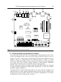
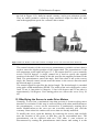
1.6 Downloading Your Design to the DE2 Board
Hooking Up the DE2 Board to the Computer
If you have a DE1, UP2 or UP3 board refer to the download Sections on those
boards. To test your design on a DE2 board as seen in Figure 1.16, plug the
USB download cable into the DE2 board’s USB connector (leftmost of the
three USB connectors on the top left side of the board) and attach the other end
to an open USB port on the PC. Using the 9V AC to DC wall transformer
attach power to the DC power connector located on the upper left corner of the
DE2 board.
Press the power switch located on the upper left edge of the board below the
power connector. When properly powered, the blue power LED on the DE2
board next to the power switch should light up and the other LEDs will flash,
if it is still setup to run the default demo design shipped from the factory.
9V DC Power
Supply
Connector
USB
Blaster
Port
USB
Device
Mic
In
USB
Host
Mic
Out
Line
In
24-bit Audio CODEC
Power
ON/OFF
Switch
XSGA
Video Port
Video
In
Ethernet
10/100M Port
RS-232
Port
27Mhz Oscillator
XSGA
10-bit DAC
USB
Host/Slave
Controller
PS/2 Port
Ethernet 10/100M
Controller
TV Decoder
(NTSC/PAL)
Altera EPCS 16
Configuration Device
Altera USB Blaster
Controller Chipset
50Mhz Oscillator
RUN/PROG
Switch for
JTAG/AS
Modes
90nm
Cyclone II
FPGA with
35K LEs
LCD 16x2 Module
8MB SDRAM
7-SEG Display Module
88 88
512KB SRAM
SD Card Connector
1MB Flash
Memory
(upgradable to
4MB)
88 88
18 Red LEDs
8 Green LEDs
IrDA
Transceiver
SMA
Ext
Clk
18 Toggle Switches
4 Push-button Switches
Figure 1.16 Altera DE2 board showing the Pushbutton and LED locations used in design (enclosed
in dashed ellipses seen in bottom right).
Tutorial I: The 15-Minute Design
23
Preparing for Downloading
Make sure that you have assigned the correct Device Name for the DE2. The
DE2 contains a EP2C35F672C6 Cyclone II FGPA. When you change the
device type you will also need to redo the pin assignments. Make sure that you
have also assigned the correct pin numbers for the DE2 board. PB1 is pin N23,
PB2 is pin P23 and the LED is pin AE23. (refer to section 1.1 for help)
Whenever you change the Device or pin assignments, if is necessary to
recompile before downloading.
After checking to make sure that the cables and jumpers are hooked up
properly, you are ready to download the compiled circuit to the DE2 board.
Select Tools Programmer. Click on Hardware Setup, select the proper
hardware, a USB-Blaster. (If a window comes up that displays, "No
Hardware" to the right of the Hardware Setup button, use the Hardware Setup
button to change currently selected hardware from "No Hardware" to "USBBlaster". If a red JTAG error message appears or the start button is not
working, close down the Programmer window and reopen it. If this still
doesn’t correct the problem, then there is something else wrong with the setup
or cable connection. Go back to the beginning of this section and check each
step and connection carefully.)
Final Steps to Download
The filename orgate.sof should be displayed in the programmer window. The
*.sof file contains the FPGA’s configuration (programming) data for your
design. To the right of the filename in the Program/Configure column, check
the Program/Configure box. To start downloading your design to the board,
click on the Start button. Just a few seconds are required to download. If
download is successful, a green info message displays in the system window
notifying you the programming was successful.
Testing Your Design
On the DE2 board, the middle two pushbuttons are used in the design and one
of the LEDs to the left just above them. The locations of PB1, PB2, and the
decimal LED are in the lower right corner of the board as seen in Figure 1.16.
After downloading your program to the DE2 board, the LED in the lower right
corner should turn off whenever a pushbutton is hit. Since the output of the OR
gate is driving the LED signal, it should be on when no pushbuttons are hit.
Since the buttons are active low, and the BNOR2 gate also has active low
inputs and output, hitting either button should turn off the LED.
24
Rapid Prototyping of Digital Systems
Chapter 1
Congratulations! You have just entered, compiled, simulated, downloaded a
design to a FPGA device, and verified its operation. Since you are using a DE2
board, you can skip the next two sections on the UP3 or UP2/1 board and go
directly to Section 1.9.
COMPLETED TUTORIAL FILES ARE AVAILABLE ON THE TEXT’S DVD.
IN THE BOOK’S DESIGN EXAMPLES, ADDITIONAL DE2 RELATED MATERIALS
AND DESIGN FILES CAN BE FOUND IN THE
DIRECTORIES.
BOOKSOFT_FE\DE2\CHAPX
Tutorial I: The 15-Minute Design
25
1.7 Downloading Your Design to the UP3 Board
Hooking Up the UP3 Board to the Computer
If you have a UP2 board skip ahead to Section 1.8. To try your design on a
UP3 board, plug the Byteblaster™ II cable into the UP3 board’s JTAG
connector (innermost of the two connectors on the left side of the board) and
attach the other end to the parallel port on the PC (USB port if you are using a
USB Blaster). If you have not done so already, make sure that the PC’s BIOS
settting for the printer port is ECP or EPP mode. Using the 6V AC to DC wall
transformer attach power to the DC power connector (DC_IN) located on the
lower right side of the UP3 board. Press in the power switch located on the
right edge of the board above the power connector. When properly powered,
two LEDs on the bottom of the UP3 board near the power connector should
light up. A USB ByteBlaster can also be used, if one is available.
Preparing for Downloading
After checking to make sure that the cables are hooked up properly, you are
ready to download the compiled circuit to the UP3 board. Select
Tools Programmer. Click on Hardware Setup, select the proper hardware,
a ByteBlasterII on LPT1. (If a window comes up that displays, No Hardware
to the right of the Hardware Setup button, use the Hardware Setup button to
change currently selected hardware from No Hardware to ByteblasterII. If a
red JTAG error message appears or the start button is not working, close down
the Programmer window and reopen it. If this still doesn’t correct the problem,
then there is something else wrong with the setup or cable connection. Go back
to the beginning of this section and check each step and connection carefully.)
The new USB ByteBlaster can also be used.
Final Steps to Download
The filename orgate.sof should be displayed in the programmer window. The
*.sof file contains the FPGA’s configuration (programming) data for your
design. To the right of the filename in the Program/Configure column, check
the Program/Configure box. To start downloading your design to the board,
click on the Start button. Just a few seconds are required to download. If
download is successful, a green info message displays in the system window
notifying you the programming was successful.
Testing Your Design
The locations of PB1, PB2, and the decimal LED are indicated in Figure 1.17.
After downloading your program to the UP3 board, the LED in the lower left
corner should turn off whenever a pushbutton is hit. Since the output of the OR
gate is driving the LED signal, it should be on when no pushbuttons are hit.
Since the buttons are active low, and the BNOR2 gate also has active low
inputs and output, hitting either button should turn off the LED.
26
Rapid Prototyping of Digital Systems
Chapter 1
Figure 1.17 ALTERA UP3 board. Pushbuttons and LED locations used in the tutorial design are
seen in the lower left corner (enclosed in dashed ellipses). Silk-screening found on the board
identifies each switch and LED.
Congratulations! You have just entered, compiled, simulated, downloaded a
design to a FPGA device, and verified its operation. Since you are using a UP3
board, you can skip the next section on the UP2 board and go directly to
Section 1.9.
COMPLETED TUTORIAL FILES ARE AVAILABLE ON THE TEXT’S DVD.
IN THE BOOK’S DESIGN EXAMPLES, ADDITIONAL UP3 RELATED MATERIALS
AND DESIGN FILES CAN BE FOUND IN THE
DIRECTORIES.
THE LARGER
BOOKSOFT_FE\UP3\CHAPX
THE \UP3\1C12\CHAPX DIRECTORIES CONTAINS DESIGNS FOR
FPGA USED ON THE 1C12 VERSION OF THE UP3
Tutorial I: The 15-Minute Design
27
1.8 Downloading Your Design to the UP2 or UP1 Board
Hooking Up the UP1 or UP 2 Board to the Computer
To try your design on a UP1 or UP2 board, plug the ByteBlaster cable into the
UP board (top left) and attach the other end to the parallel port on a PC. If you
have not done so already, make sure that the PC’s BIOS settting for the printer
port is ECP or EPP mode. Using a 9V AC to DC wall transformer or another 7
to 9V DC power source, attach power to the DC power connector (DC_IN)
located on the upper left-hand corner of the UP3 board. When properly
powered, one of the green LEDs on the board should light up.
Figure 1.18 ALTERA UP2 board with jumper settings and PB1, PB2, and LED locations.
Verify that the device jumpers are set for the FLEX chip as shown in Table 1.2.
The locations of the pushbuttons, PB1 and PB2, and the LED decimal point are
also highlighted in Figure 1.18. (Note that for the MAX EPM7128 chip, the
jumper pins are all set to the top position as indicated in Table 1.2.)
Table 1.2 Jumper settings for downloading to the MAX and FLEX devices.
28
Rapid Prototyping of Digital Systems
Chapter 1
Preparing for Downloading
After checking to make sure that the cables and jumpers are hooked up
properly, you are ready to download the compiled circuit to the UP2 board.
Select Tools Programmer. Click on Hardware Setup, select the proper
hardware, a ByteBlasterII on LPT1. (If a window comes up that displays, "No
Hardware" to the right of the Hardware Setup button, use the Hardware Setup
button to change currently selected hardware from "No Hardware" to
"ByteBlasterII". If a red JTAG error message appears or the start button is not
working, close down the Programmer window and reopen it. If this still
doesn’t correct the problem, then there is something else wrong with the setup
or cable connection. Go back to the beginning of this section and check each
step and connection carefully.) The new USB ByteBlaster can also be used.
Final Steps to Download
Make sure that the Device Name has changed to EP10K20 or
EPF10K20RC240 for the UP1 or EPF10K70RC240 for the UP2 (depending
on the UP board and Quartus II version that you are running). Make sure you
have also assigned the pin numbers for a UP2 board (see Table 1.1). If it does
not display the correct device, then return to your schematic, assign the correct
device first and then the pin numbers (See section 1.1.), recompile, and try
again. Next, check the Program/Configure box.
The Start button in the programming window should now be highlighted.
Click on the Start button to download to the UP2 board. Just a few seconds are
required to download. If download is successful, a green info successful
programmer operation message displays in the system window. (If the Start
button is not highlighted, click Hardware Setup from the programmer
window. Confirm the port settings and click OK. If you still have problems
confirm that the printer port BIOS settings use ECP or EPP mode.)
Testing Your Design
The locations of PB1, PB2, and the decimal LED are indicated in Figure 1.19.
On the UP2, one of the seven-segment LEDs decimal points is used for
monitoring the LED output.
Pin 14
Figure 1.19 UP2’s FLEX FPGA pin connection to seven-segment display decimal point.
All of these LEDs are pre-wired to the FPGA chip with a pull-up resistor as
illustrated earlier in Figure 1.6. This configuration allows the external resistor
Tutorial I: The 15-Minute Design
29
to control the amount of current through the LED; however, it also requires the
FPGA chip to output a Low signal to turn on the LED. (Students regularly
forget this point and have a fully working project with an inverted pattern on
the LEDs.). Vcc is 5V on the UP2.
Figure 1.19 shows the UP2’s Flex FPGA pin number 14 hard wired to the
seven-segment LEDs decimal point. On the UP2, in this tutorial, only the
decimal point will be used for output.
After downloading your program to the UP2 board, locate the two rightmost
seven-segment displays. Since the output of the BNOR2 gate is driving the
decimal LED signal on the left digit of the two seven-segment displays, it
should be off (i.e., LED state is inverted on UP1 and UP2). Since the buttons
are active low, and the BNOR2 gate also has active low inputs and output,
hitting either button should turn on the LED.
Congratulations! You have just entered, compiled, simulated, and downloaded
a design to a FPGA device, and verified its operation.
COMPLETED TUTORIAL FILES ARE AVAILABLE ON THE TEXT’S DVD.
IN THE BOOK’S DESIGN EXAMPLES, ADDITIONAL UP2 RELATED MATERIALS
CAN BE FOUND IN THE
BOOKSOFT_FE\UP2\CHAPX DIRECTORIES.
ADDITIONAL UP RELATED MATERIALS CAN BE FOUND IN THE
\UP1\CHAPX DIRECTORIES.
1.9 The 10 Minute VHDL Entry Tutorial
As an alternative to schematic capture, a hardware description language such
as VHDL or Verilog can be used. In large designs, these languages greatly
increase productivity and reduce design cycle time. Logic minimization and
synthesis to a netlist are automatically performed by the compiler and
synthesis tools. (A netlist is a textual representation of a schematic.) As an
example, to perform addition, the VHDL statement:
A <= B + C;
will automatically generate an addition logic circuit with the correct number of
bits to generate the new value of A. Using the OR-gate design from the
Schematic Entry Tutorial, we will now create the same circuit using VHDL.
PRIOR KNOWLEDGE OF VHDL IS NOT NEEDED TO COMPLETE THIS TUTORIAL .
30
Rapid Prototyping of Digital Systems
Chapter 1
Using a Template to Begin the Entry Process
Choose File New, select VHDL File and OK. Place the cursor within the
text area, right click the mouse, and select Insert Template. Make sure VHDL
is selected. (Note the different prewritten templates. These are provided to
expedite the entry of VHDL.) Select VHDL Constructs Design
Units Entity Declaration. This template is the one you will generally start
with since it also sets up the input and output declarations. The template for
the ENTITY declaration appears in the Insert Template preview window. Click
Insert and then Close to paste the template in your VHDL window. Since the
editor knows that it is a VHDL source file, the text will appear in different
context-sensitive colors. VHDL keywords appear in blue and strings in purple
and comments are green. The color information should be used to detect minor
syntax errors while still in the text editor.
Saving the VHDL Source File
Select File
Save As and save the file as orgate.vhd – click Save.
Replacing Comments in the VHDL Code
The entire string indicating the position of the entity name, <entity_name>,
should be set to the name used for the filename – in this case, orgate. There
are two occurrences of <entity_name> in the text. Find and change both
accordingly.
Declaring the I/O Pins
The input and output pins, PB1, PB2 and LED need to be specified in the
PORT declaration. Since there are no input vectors, bi-directional I/O pins, or
GENERIC declarations in this design, remove all of these lines. The source
file should look like Figure 1.20.
Figure 1.20 VHDL Entity declaration text.
Tutorial I: The 15-Minute Design
31
Setting up the Architecture Body
Click the mouse at the bottom of the text field. (We will be inserting another
template here.) Following the earlier procedure for selecting a VHDL template
(start with a right click), select VHDL Constructs Design
Units Architecture Body. (The Architecture Body specifies the internal
logic of the design.) The syntax for the Architecture Body appears in the text
window after the other text. (You can now see why the template is left
highlighted – had you not placed your cursor first, text would have appeared at
your last cursor position. If you do misplace the template, hitting the Edit
Undo key removes the new text.)
Editing the Architecture Body
Change the entity name in the ARCHITECTURE statement to orgate.
Template lines with a "--" preceding a comment, need to be edited
appropriately for each particular design. Delete the signal declaration line
since this simple design does not require internal signals. Delete the remaining
comment lines after BEGIN that start with "--", and insert LED <= NOT (
NOT PB1 OR NOT PB2 ) as a single line. (This line contains a deliberate
syntax error that will be detected and fixed later.) Insert the following two
lines at the beginning of the text file to define the libraries for the
STD_LOGIC data type.
LIBRARY IEEE;
USE IEEE.STD_LOGIC_1164.all;
This is the preferred data type for bits in VHDL. The file should now appear
similar to Figure 1.21.
Figure 1.21 VHDL OR-gate model (with syntax error).
32
Rapid Prototyping of Digital Systems
Chapter 1
Before You Compile
Before you compile the VHDL code, the FPGA device type and pin numbers
need to be assigned with Assignments Device and Assignments Pin. If
your pins are already defined from the earlier Schematic Entry Tutorial, just
confirm the pin assignments. If you did not do this step earlier in the tutorial
see the device and pin assignment instructions at the end of section 1.1. At this
point, VHDL code is generally ready to be compiled, simulated, and
downloaded to the board using steps identical to those used earlier in the
schematic entry method. Once pin assignments are made, they are stored in the
project’s *.qsf file.
1.10 Compiling the VHDL Design
The Compile process checks for syntax errors, synthesizes the logic design,
produces timing information for simulation, fits the design on the FPGA, and
generates the file required to program the FPGA. After any changes are made
to the design files or pin assignments, the project should always be recompiled prior to simulation or programming.
Figure 1.22 VHDL compilation with a syntax error.
Select Project ADD/Remove Files in Current Project. Confirm that the
new orgrate.vhd file is now part of project and remove the tutorial’s earlier
Tutorial I: The 15-Minute Design
33
orgate.bdf file that the new VHDL file replaces from the project’s file list, if it
is present. Click OK. Start the compiler with Processing Start
Compilation.
Checking for Compile Warnings and Errors
The project should compile with an error. After compiling the VHDL code, a
window indicating an error should appear. The result should look something
like Figure 1.22.
Double click on the first red error line and note that the cursor is placed in the
editor either on or after the line missing the semicolon (;). VHDL statements
should end with a semicolon. Add the semicolon to the end of the line so that it
is now reads:
LED <= NOT ( NOT PB1 OR NOT PB2 );
Now, recompile, and you should have no errors. You can simulate your VHDL
code using steps identical to the tutorial’s earlier schematic version of the
project.
Viewing the Synthesized Logic in a Schematic
You can view the logic automatically generated by the VHDL synthesis tools
using Tools Netlist Viewers RTL Schematic, after a successful
compilation. A schematic of the logic synthesized by your VHDL code will be
displayed as seen in Figure 1.23. This is a handy way to double check simple
logic designs when first becoming familiar with VHDL or Verilog hardware
description languages and their associated automatic logic synthesis tools.
Figure 1.23 Logic schematic that was automatically synthesized from the VHDL code.
34
Rapid Prototyping of Digital Systems
Chapter 1
1.11 The 10 Minute Verilog Entry Tutorial
Verilog is another widely used hardware description language (HDL). Verilog
and VHDL have roughly the same capabilites. VHDL is based on a PASCAL
style syntax and Verilog is based on the C language. In large designs, HDLs
greatly increase productivity and reduce design cycle time. Logic minimization
and synthesis are automatically performed by the compiler and synthesis tools.
Just like the previous VHDL example, to perform addition, the Verilog
statement:
A = B + C;
will automatically generate an addition logic circuit with the correct number of
bits to generate the new value of A.
Using the OR-gate design from the Schematic Entry Tutorial and the VHDL
Tutorial, we will now create the same circuit in Verilog.
PRIOR KNOWLEDGE OF VERILOG IS NOT NEEDED TO COMPLETE THIS TUTORIAL.
Using a Template to Begin the Entry Process
Choose File New, select Verilog HDL File and OK. Place the cursor within
the text area, right click the mouse, and select Insert Template and then select
Verilog HDL. (Note the different prewritten templates. These are built to
expedite the entry of Verilog.) Select Constructs Design Units Module
Declaration (style 2) – this declaration is the one you will generally start with
since it also sets up the input and output declarations. Click Insert then Close
and the template for the module declaration appears in the Text editor. Since
the editor knows that it is a Verilog source file, the text will appear in different
context-sensitive colors. Verilog keywords appear in blue and strings in purple
and comments in green. The color information should be used to detect minor
syntax errors while still in the text editor.
Saving the new Verilog File
Select File Save As. Note the automatic extension is .v (Verilog) and save
the file as orgate.v – click Save.
Replacing Comments in the Verilog Code
The entire string indicating the position of the entity name, <module_name>,
should be set to the name used for the filename – in this case, orgate. There is
one occurrence of <module_name> in the text. Find and change it
accordingly. Lines starting with // are comments and these will need to be
replaced with the appropriate Verilog code.
Tutorial I: The 15-Minute Design
35
Declaring the I/O Pins
The input pins, PB1 and PB2, and the output pin, LED, need to be specified in
the arguments of the Module statement and Port declaration. Since there are no
‘inout pins’, ‘wire’, ‘reg’, or ‘integer’ declarations, or Always statements in
this design, remove all of these lines. The source file should now look similar
to Figure 1.24.
Figure 1.24 Verilog module declaration text.
Setting up the Behavioral Code
Click the mouse to just before the line starting with “endmodule”. (We will be
inserting another template here.) Following the earlier procedure for selecting
a Verilog template (start with a right click), select a Constructs Module
Items Continuous Assignment. (A single assign statement will specify the
internal logic of this design.) The syntax for a Continuous Assignment
Statement appears in the text window after the other text. (You can now see
why the template is left highlighted – had you not placed your cursor first, text
would have appeared at your last cursor position. If you do misplace the
template, hitting the delete key removes the highlighted text.)
Editing the Continuous Assignment Statement
Change the <net lvalue> in the assign statement to "LED" and <value> to:
! ( ! PB1 | ! PB2 );
Verilog is based on C and "|" (vertical line) is the bit wise OR operator. The "!"
(exclamation point) is the NOT operator. Delete the remaining comment lines
that start with "//". Delete the ";" at the end of the assign LED statement (This
causes a deliberate syntax error that will be detected and fixed later.) The file
should now appear as in Figure 1.25.
36
Rapid Prototyping of Digital Systems
Chapter 1
Before You Compile
Before you compile the Verilog code, the FPGA device type and pin numbers
need to be assigned with Assignments Device and Assignments Pin. If
your pins are already defined from the earlier Schematic Entry Tutorial, just
confirm the pin assignments. If you did not do this step earlier in the tutorial
see the device and pin assignment instructions at the end of Section 1.1.
Figure 1.25 Verilog active low OR-gate model (with syntax error).
At this point, Verilog code is generally ready to be compiled, simulated, and
downloaded to the board using steps identical to those used earlier in the
schematic entry method. Once pin assignments are made, they are stored in the
project’s *.qsf file.
1.12 Compiling the Verilog Design
The Compile process checks for syntax errors, synthesizes the logic design,
produces timing information for simulation, fits the design on the FPGA, and
generates the file required to program the FPGA. After any changes are made
to the design files or pin assignments, the project should always be recompiled prior to simulation or programming.
Select Project ADD/Remove Files in Current Project. Confirm that the
new orgrate.v file is now part of project and remove the tutorial’s earlier
orgate.bdf or orgate.vhd files that the new Verilog file replaces from the
project if either file is present. Click OK. Start the compiler with
Processing Start Compilation.
Tutorial I: The 15-Minute Design
37
Checking for Compile Warnings and Errors
The project will compile with an error. After compiling the Verilog code, a
window indicating an error should appear. (See Figure 1.26.)
Figure 1.26 Verilog compilation with a syntax error.
Double click on the first red error line and note that the cursor is placed in the
editor either on or after the line missing the semicolon (;). Verilog statements
should end with a semicolon. Add the semicolon to the end of the line so that it
is now reads:
assign LED = ! ( ! PB1 | ! PB2 );
Now, recompile, and you should have no errors. You can simulate your Verilog
code using steps identical to the tutorial’s earlier schematic version of the
project. You can also view a schematic of the synthesized logic using
Tools Netlist Viewers RTL Schematic similar to the steps previously
outlined in the VHDL tutorial.
38
Rapid Prototyping of Digital Systems
Chapter 1
1.13 Timing Analysis
With every physical device, there are timing considerations. An FPGA’s timing
is affected by:
•
•
•
•
Input buffer delays,
Signal routing interconnect delays within the FPGA,
The internal logic delays (in this case the OR), and
Output buffer delays.
The timing analysis tool can be used to determine:
•
•
The physical delay times and
The maximum clock rates in your design.
Starting the Analyzer
At the top menu, select Processing Compilation Report and then in the
Compilation Report window, expand Timing Analyzer and select tpd. A
matrix of input to output delay times for the project will be computed and
displayed as seen in Figure 1.27.
Figure 1.27 Timing analyzer showing input to output signal propagation timing delays.
Note that this is the same delay time seen in the simulator. These times include
the input-to-output buffer delays at the pins and the interconnect delays inside
the FPGA. The internal OR logic delay is only around a nanosecond relative to
the rest of the device delay.
The exact time shown will vary with different versions of the Altera CAD
tools, the different FPGA chips found on the various boards, and different
FPGA chip speed grades. Other timing analysis options include setup times,
hold times, and clock rates for sequential circuits.
Tutorial I: The 15-Minute Design
39
1.14 The Floorplan Editor
A floorplan editor is a visual tool to assist expert users in manually placing and
moving portions of logic circuits to different logic cells inside the FPGA. This
is done in an attempt to achieve faster timing or better utilization of the FPGA.
Floorplanning is typically used only on very large designs that contain
subsections of hardware with critical high-speed timing. Since the interconnect
delays are as large as the design’s logic delays, logic element and I/O pin
placement is very critical in high speed designs. Vertical and horizontal
interconnect buses are used through the FPGA to connect Logic Elements.
For all but expert users, the compiler’s automatic place-and-route tools should
be used. Automatic place-and-route was already performed by the fitter in the
compile process of the tutorial. Timing constraints for critical signals can also
be specified in some FPGA place and routing tools to help the fitter meet the
design’s timing goals.
To see the fitter’s automatic placement of the design inside the FPGA, select
Assignment Back-Annotate
Assignments
click
OK
and
then
Assignments Timing Closure Floorplan. In the display that opens, zoom in
and scroll around to find the colored logic element and gray shaded I/O pins
used in your design. Find and select the colored Logic Element (LE), then
View Routing show fan in and then show fan out, and a view like Figure
1.28 showing the design can be produced for the DE1.
There is a lot of empty space since the Cyclone II EP2C20 FPGA contains
18,752 Logic Elements (LEs) and 315 I/O pins. Only 1 LE and three I/O pins
were used in this design. If you move the logic cell or I/O pins to other
locations, it will make small changes to the circuit timing because of changes
in the interconnect delays inside the FPGA.
Due to the vast number of possible combinations, FPGA CAD tools cannot
explore every possible placement and routing option. The Quartus II Design
Space Explorer tool can also be used to search and explore other design
options in the design space. Large FPGA designs containing millions of gates
can require several hours or even days of CPU time to examine many of the
different place and route alternatives in the design space.
40
Rapid Prototyping of Digital Systems
Chapter 1
Figure 1.28 Floorplan view showing the internal FPGA I/O and LE placements of an OR-gate on a
DE1. User logic and pins used in the design are seen as shaded areas in the lower right corner.
1.15 Symbols and Hierarchy
The Symbol Editor is used to edit or create a symbol to represent a logic
circuit. Symbols can be created for a design whenever a VHDL or Verilog file
is compiled. Create a symbol for your VHDL design by opening the orgate.vhd
file, and then select File Create/Update Create Symbol Files for
Current File.
Select File Open, change the file type setting for *.bsf, find and chose
orgate.bsf to see the new symbol for your VHDL based design as shown in
Figure 1.29. Inputs are typically shown on the left side of the symbol and
outputs on the right side. Symbols are used for design hierarchy in more
complex schematics. This new symbol can be used to add the circuit to a
design with the graphic editor just like the BNOR2 symbol that was used
earlier in the tutorial. Double clicking on a symbol in the graphic editor will
open a pop-up requesting, “Select one design file.” Selecting the appropriate
*.vhd, *.v, or *.bdf, file takes the user to the underlying Verilog, VHDL, or
graphic file respectively by opening the underlying file in a different screen
tab.
Tutorial I: The 15-Minute Design
41
orgate
PB1
LED
PB2
inst
Figure 1.29 ORgate design symbol.
1.16 Functional Simulation
In large designs with long compile and simulation times, a faster functional
simulation is commonly used initially. This type of simulation does not include
device delay times and it is used solely to check for logic errors. Although a
functional simulation is good for finding logic errors, a timing simulation is
still necessary to check for any timing related errors as illustrated earlier in the
tutorial.
Performing a Functional Simulation
To perform a functional simulation, set the simulator for functional simulation
with Assignments Settings. Select Simulator Settings in the left column
and then change the simulation mode from Timing to Functional. Run
Processing Generate Functional Simulation Netlist. Finally, select
Processing Start Simulation. Open the Simulation Report waveform and
note that the output changes without any delay in response to an input, unlike
the earlier timing simulation. To switch back to a timing-mode simulation,
change the simulator setting back to timing, recompile, and restart the
simulation.
This short tutorial has gone through the basics of a simple design using a
common path through the design tools. As you continue to work with the tools,
you will want to explore more of the menus, options and shortcuts. Chapter 4
contains a tutorial that will introduce a more complex design example. In
Quartus II, Help Tutorial also contains more tutorials. Quartus II video
tutorials and reference manuals are also available online at Altera’s website,
www.altera.com .
A number of files such as the *.q* files are maintained in the project directory
to support a design. Appendix B contains a list of different file extensions used
by Quartus II. One of the more important files in a project is the *.qsf file. It
contains the device type and pin assignments along with a number of other
project settings.
42
Rapid Prototyping of Digital Systems
Chapter 1
1.17 Laboratory Exercises
1. The tutorials ORed the active low signals from the pushbuttons and produced an output
that was required to be low to turn off an LED. This was accomplished with the
"negative-logic OR" gate illustrated to the left in Figure 1.30.
A + B = A B
Figure 1.30 Equivalent gates: A negative logic OR and a positive-logic AND.
We know from DeMorgan's Law that the equation in Figure 1.25 represents an
equivalence. We should therefore be able to substitute a simple two-input AND gate as
illustrated in Figure 1.29 and accomplish the same task as the single gate used in the
tutorial. Substitute the AND2 gate for the BNOR2 gate in the schematic capture, then
compile, simulate, and download the AND circuit. What can you conclude?
2. Substitute in the VHDL code:
LED <= PB1 AND PB2;
Or into the Verilog code:
assign LED = PB1 & PB2;
Compile, simulate, and download and test the new circuit. What can you conclude about
gate equivalence using DeMorgan’s Theorem?
3. Design a logic circuit to turn on the LED when both pushbuttons are pressed. Compile,
simulate, and download the new circuit.
4. Try a different logic function such as XOR. Start at the beginning or edit your existing
schematic by deleting and replacing the BNOR2 symbol. Next repeat the tutorial steps to
compile, simulate, download and test.
5. Repeat problem 2 for all of the basic gates including, OR, NOR, NAND, XOR, XNOR,
and NOT. Try using different LEDs and output your results simultaneously. Look up the
pin connections for the FPGA chip in Table 2.4 and be sure to give each pinout a
different name.
6. Design, enter, simulate and implement a more complex logic gate network. One
suggestion is a half adder. You will need two LED outputs.
Tutorial I: The 15-Minute Design
43
7. In the schematic editor, try building the design with some 74xx TTL parts from the
others maxplus2 symbol library.
8. Draw a schematic and develop a simulation to test the 2-to-1 Mux function in the others
maxplus2 symbol library.
9. View the orgate.rpt file and find the device utilization, the pin assignments, and the
netlist. A substantial portion of the time delay in this simple logic design is the input and
output buffer delays and the internal routing of this signal inside the FPGA. Find this
delay time by removing the BNOR2 gate and one of the inputs in the schematic.
Connect the input pin to the output pin, recompile and rerun the timing analyzer to
estimate this time delay.
10. Use the chip editor to move the logic cell used in the OR-gate design to another location
inside the FPGA. For information of the chip editor, use the Quartus II Help function.
Try moving the LE used several columns farther away from the pushbutton and LED
pins. Not all locations of the logic cell will work and some trial and error will be
required. Save the edited design, rerun the timing analyzer, and compare the resulting
time delays with the original time delays. See if you are able to achieve a faster
implementation than the automatic place-and-route tools.
11. Remove the pin number constraints from the schematic and let the compiler assign the
pin locations. Rerun the timing analyzer and compare the time delays. Are they faster or
slower than having specified the input pins?
12. If you are using a UP2 board, retarget the example design to the MAX chip. Pin
numbers for the MAX decimal point LED can be found in the UP2 User manual. It will
be necessary to connect jumper wires from the MAX header to the pushbuttons. Select
pins near the pushbuttons. Pin numbers can be seen on the board’s silk-screen. Compare
the timing from the MAX implementation to the Flex implementation.
13. If a storage oscilloscope or a fast logic analyzer is available, compare the predicted
delay times from the simulation and timing analysis to the actual delays measured on the
FPGA board. Force the pins to a header connector so that you can attach probes to the
signal wires.
14. Draw a schematic that uses the LPM_ADD_SUB megafunction to add two signed
numbers on the Cyclone device. Use Tools
Megawizard to start the megawizard to
help configure LPM symbols. Verify the proper operation using a simulation with two 4bit numbers. Do not use pipelining, clock, or carry in. Vary the number of bits in the
adder and find the maximum delay time using the timing analyzer. Plot delay time
versus number of bits for adder sizes of 4, 8, 16, 32, and 64 bits. Using the LC
percentages listed in the compiler’s report file, estimate the hardware size in LEs. Plot
LEs required versus number of bits.
44
Rapid Prototyping of Digital Systems
Chapter 1
15. Use the DFF part from the primitives storage library and enter the symbol in a schematic
using the graphical editor. Develop a simulation that exercises all of the features of the
D flip-flop. Use Help on DFF for more information on this primitive.
16. Use the DFFE part from the primitives storage library and enter the symbol in a
schematic using the graphical editor. Develop a simulation that exercises all of the
features of the D flip-flop with a clock enable. Use Help on DFFE for more information
on this primitive.
17. Use gates and a DFF part from the primitives storage library with graphical entry to
implement the state machine shown in the following state diagram. Verify correct
operation with a simulation using the Altera CAD tools. The simulation should exercise
all arcs in the state diagram. A and B are the two states, X is the output and Y is the
input. Use the timing analyzer’s Processing
Classic Timing Analyzer Tool
Registered performance option tab to determine the maximum clock frequency on the
Cyclone device. Reset is asynchronous and the DFF Q output should be high for state B.
1
1
A
X=0
Reset
0
B
X=1
0
18. Repeat the previous problem but use one-hot encoding on the state machine. For one-hot
encoding use two flip-flops with only one active for each state. For state A the flip-flop
outputs would be "10" and for state B "01". One-hot encoding is common in FPGAs.
CHAPTER 2
FPGA Development Board
Hardware and I/O Features
Photo: The Altera DE1 board contains a Cyclone II FPGA, external SRAM, SDRAM &
Flash memory, and a wide assortment of I/O devices and connectors.
46
Rapid Prototyping of Digital Systems
Chapter 2
2 FPGA Development Board Hardware and I/O Features
Each of the five different FPGA boards (DE1, DE1, UP3, UP2, and UP1) have
a slightly different feature set of logic, I/O interfaces, memory and other
assorted hardware. As long as the FPGA board has enough logic and it has the
required I/O features, a project can be implemented on any of the boards.
FPGAs are available in a wide range of sizes with different feature sets. In
general, FPGAs with more logic, more I/O pins, higher speed, or more memory
are more expensive. When designing new products, choosing the FPGA with
the proper feature set at the lowest cost is an important design consideration.
Figure 2.1 The Altera DE1 board has a number of onboard I/O devices.
FPGA Development Board Hardware and I/O Features
7.5V DC Power
Supply
Connector
USB
Blaster
Port
Mic
In
Line
In
Line
Out
47
RS-232
Port
VGA
Video Port
PS/2 Port
Power
ON/OFF
Switch
24-bit Audio CODEC
Ocillators
27Mhz 50MHz 24Mhz
Altera USB
Blaster
Controller
Chipset
Altera EPCS 16
Configuration Device
RUN/PROG
Switch for
JTAG/AS
Modes
90nm
Cyclone II
FPGA with
20K LEs
8MB SDRAM
512KB SRAM
SD Card Socket
4MB Flash
Memory
7-SEG Display Module
8 Green LEDs
10 Red LEDs
SMA
External
Clock
4 Push-button Switches
10 Toggle Switches
Figure 2.2 The Altera DE1 board’s I/O features.
2.1 FPGA and External Hardware Features
On each of the boards, the FPGA is the large square chip located near the center
of the development board. Locate the FPGA chip on the DE1 board as seen in
Figures 2.1 and 2.2. Each of the various board’s FPGAs has a different array of
features. These are summarized for the different boards in Table 2.1. Each
FPGA has a different number of logic elements (LE) that are used to implement
user logic. They also contain varying amounts of both internal embedded
memory blocks and the newer boards also have external memory.
FPGAs such as the Cyclone II found on the DE1 and DE2 boards are designed
to support Digital Signal Processing (DSP) applications, so they also contain
hardware integer multipliers.
On larger FPGAs, phase locked loops (PLLs) are used to divide, multiply, and
shift the phase of clock signals. Remember that you must always compile your
design for the correct board’s FPGA device and pin assignments or it will not
download to the device and operate correctly.
48
Rapid Prototyping of Digital Systems
Chapter 2
Table 2.1 FPGA and Hardware Features of the different development boards.
FPGA & Hardware
Features
Introduction Year
FPGA Family
Logic Elements
(LEs)
Approximate Max.
Logic Gate Count1
DE1
DE2
UP3
UP2 & 1
2006
Cyclone II
2006
Cyclone II
18,752
35,000
500,000
1,000,000
FPGA Device Part
Number
EP2C20F484C7
EP2C35F672
C6
Memory in bits
204K bits
483K bits
PLLs
Integer 18 by 18 bit
Multipliers
External
Clocks
External SRAM
Memory
External SDRAM
Memory
Ext. Flash
Memory
Nios II Processor
SoC Designs
Supported
4
4
2004
Cyclone
6,000 (1C6) or
12,000 (1C12)
189,000 (1C6)
or 378,000
EP1C6Q240C8
or (1C12)
EP1C12Q240C
8
80K or 208K
bits
2
2001 & 1999
Flex10K
3,744 or 1,152
(UP1)
118,000 or
63,000(UP1)
EPF10K70
RC240-4 or
EPF10K20
RC240-4 (UP1)
18K bits
12K (UP1)
No
26
35
No
No
24, 27, 50 Mhz
27, 50Mhz
48, 66, or
100Mhz
25Mhz
64k by 16 bits
No
1M by 16 bits
No
1M by 16 bits
with 4 banks
256K by 16
bits
1M by 16 bits
with 4 banks
4M by 8 bits
4M by 8 bits
1M by 8 bits
No
Yes
Yes
Yes
No
256K by 16 bits
2.2 The FPGA Board’s Memory Features
In addition to the FPGA’s internal memory, the newer boards provide several
external ROM and RAM memory devices as seen in Table 2.1. Capacities of
external memory are much larger than the internal memory, but they will have a
slower access time.
FPGA processor cores such as the Nios II used in System-on-a-Chip (SoC)
designs use external memory for program and data memory, and typically use
the FPGA’s smaller and faster internal memory for register files and a cache.
Flash and EEPROM are used to provide non-volatile memory storage. The
EPCS1 serial Flash chip is used to automatically load the FPGA’s serial
configuration data at power up in final systems where you do not want to
download the board with the ByteBlaster each time power is applied.
1
This is only a very crude estimate of the number of equivalent two input NANDs in the FPGA’s hardware
design. This should be viewed only as a very rough estimate since any real design cannot use every feature
of every logic element. The estimates given here also include additional gates in the total count to account
for the FPGA’s embedded memory blocks and hardware multipliers. Such crude gate count estimates can
also vary by a factor of two or more between different FPGA venders for a similar device and they are
rarely used now in industry.
FPGA Development Board Hardware and I/O Features
49
A larger Flash memory chip is typically used to boot the initial program code
on SoC designs that include a processor. Note that the older UP2 and UP1s
cannot support a Nios processor since they lack external memory and have a
smaller older FPGA. Links to detailed datasheets for many of the different
board’s memory chips can be found on the book’s DVD or at the book’s
website.
Each board contains a crystal controlled clock circuit that is normally used as
the master clock for the user’s digital logic circuit. Note that the frequency of
the clock is different on the boards as seen in table 2.1. PLLs can be used to
scale the crystal controlled clock to provide other clock frequencies.
2.3 The FPGA Board’s I/O Features
Each board provides a wide variety of I/O features as summarized in Table 2.2.
For most devices, the FPGA board’s hardware provides only an electrical
interface to the FPGA’s I/O pins. Logic that provides a device interface circuit
or controller will need to be constructed by the user using the FPGA’s internal
logic. Many design examples of interfacing to these various I/O devices can be
found in the following chapters of this book.
Standard 0.1 inch headers on each of the boards can be used to interface to
external devices off of the board. A small custom PCB can be designed or a 0.1
inch predrilled perforated protoboard can be used to plug into the header
connectors on the board. Standard 0.1 inch ribbon cable connector technology
can also be used to connect to another board with custom user hardware.
Table 2.2 The I/O Features of the different development boards.
I/O Features
Pushbuttons
User Switches
User LEDs
LCD Panel
Seven Segment
LED Displays
PS/2
RS-232 Serial
VGA output
I/O Expansion
Header Pins
TV Decoder
SD Card slot
Printer Port
Audio CODEC
User USB
IrDA
Network
Optional Camera
and Color LCD
Panel
DE1
4 - debounced
18
8 green 10 red
No
4
DE2
4 - debounced
10
9 green 18 red
16 char x 2 line
8
UP3
4 –no debounce
4
4
16 char x 2 line
No
UP1& 2
2 –no debounce
8
No
No
2
Yes
Yes
212 colors
2 – 40 Pin
connectors
No
Yes
No
24-bit
No
No
No
Yes
Yes
Yes
230 colors
2 – 40 Pin
connectors
Yes
Yes
No
24-bit
Yes
Yes
10/100Mhz
Yes
Yes
Yes
8 colors
4 – 72 I/O Pins
total
No
No
Yes
No
No
No
No
No
Yes
No
8 colors
3 – add 60 Pin
headers
No
No
No
No
No
No
No
No
50
Rapid Prototyping of Digital Systems
Chapter 2
Modern FPGAs are surface-mount chips that are soldered directly to the board.
It is difficult if not impossible to replace the FPGA chip without expensive
surface mount soldering equipment, so extreme care should be exercised when
interfacing the FPGA I/O pins to any external devices.
Standard I/O connector pin assignments used for external PS/2, serial, parallel,
VGA, network and USB I/O cables can be found in Appendix F.
Table 2.3 Requirements to use the different I/O Features
I/O Device
Description
USB 1.1
Full Speed and Low Speed
Serial Port
Parallel Port
PS/2 Port
VGA Port for
Video Display on
Monitor
IDE Port
Reset Switch
Pushbutton
Switches
Hardware Interface Needed
Processor & USB SIE engine core
RS 232 Full Modem
UART to send and receive data
IEEE 1284
State machine or Proc. for handshake
PC Keyboard or Mouse
Serial Data - PS/2 state machine
RGB three 1-bit signals on
UP1,2,3, 10-bits on DE2
and 3-bits on DE1
State machine for sync signals & user
logic to generate RGB color signals
Connector on UP3
Processor & IDE Device Driver
Global Reset on UP3
Must use a reset in design
debounced on DE1 & DE2
but not on the UP1,2, & 3
Most applications will need a switch
debounce Circuit on UP1,2,3
Connect to .1 inch headers
Depends on expansion card used
1=ON (DE1 & DE2)
None, but uses 1 FPGA I/O pin
LCD Display
16 Character by 2 line
ASCII Characters
on DE2& UP3
State machine or Processor to send
ASCII characters and LCD commands
Real Time Clock
I2C clock chip on UP3
Serial Data - I2C state machine
DIP/Slide Switch
Switches (1=ON)
None or Synchronizer Circuit
Expansion Cards
LEDs
W HEN CONNECTING EXTERNAL HARDWARE, ADDITIONAL PINS ARE AVAILABLE FOR USE ON
THE HEADER CONNECTORS ON THE BOARD . F OR DETAILS, REFER TO THE BOARD’ S
REFERENCE MANUAL, WHICH IS ON THE BOOK’S DVD, AND IS ALSO AVAILABLE FREE AT
HTTP:// WWW.ALTERA.COM OR AT HTTP:// WWW.TERASIC .COM.
Also, remember to assign pins as shown in the tutorials to avoid randomly
turning on several of the memory devices at the same time. A tri-state bus
conflict occurs when several tri-state outputs are turned on and they attempt to
drive a single signal line to different logic levels. It is possible that such a tristate bus conflict on the memory data bus could damage the devices by
overheating after several minutes of operation.
Table 2.4 contains the pin assignments and names used for the DE1, DE2, UP3,
and UP2 board’s most commonly used I/O devices that are used in basic digital
designs. A complete list of all pin assignments for all of the boards is too
lengthy to include here; however, they can be found in each of the FPGA
board’s user manuals that are available on the book’s DVD in \Board\Chap2.
FPGA Development Board Hardware and I/O Features
51
Table 2.4 DE1, DE2, UP3, and UP2 Board’s FPGA I/O pin names and assignments
Pin Name
DE1
DE2
UP3
UP2,
UP1
Pin
Type
Function of Pin
KEY0
R22
G26
48
28 PB1
Input
Pushbutton KEY0
(debounced, 0 = button hit)
KEY1
R21
N23
49
29 PB2
Input
Pushbutton KEY1
(debounced, 0 = button hit)
KEY2
T22
P23
57
-
Input
Pushbutton KEY2
(debounced, 0 = button hit)
KEY3
T21
W26
62
-
Input
Pushbutton KEY3
(debounced, 0 = button hit)
LEDR0
R20
AE23
56
25
0=on
Output
RED LED R0
(1 = LED ON, 0= LED OFF)
LEDR1
R19
AF23
55
14
0=on
Output
RED LED R1
(1 = LED ON, 0= LED OFF)
LEDR2
U19
AB21
54
-
Output
RED LED R2
(1 = LED ON, 0= LED OFF)
LEDR3
Y19
AC22
53
-
Output
RED LED R3
(1 = LED ON, 0= LED OFF)
SW0
L22
N25
58
41
Input
Slide or DIP Switch
(0=Down, non-debounced)
SW1
L21
N26
59
40
Input
Slide or DIP Switch
(0=Down, non-debounced)
SW2
M22
P25
60
39
Input
Slide or DIP Switch
(0=Down, non-debounced)
SW3
V12
AE14
61
38
Input
Slide or DIP Switch
(0=Down, non-debounced)
HEX0[0]
J2
AF10
-
6
Output
Seven Segment Display 0
LED Segment A (0=on)
HEX0[1]
J1
AB12
-
7
Output
Seven Segment Display 0
LED Segment B (0=on)
HEX0[2]
H2
AC12
-
8
Output
Seven Segment Display 0
LED Segment C (0=on)
HEX0[3]
H1
AD11
-
9
Output
Seven Segment Display 0
LED Segment D (0=on)
HEX0[4]
F2
AE11
-
11
Output
Seven Segment Display 0
LED Segment E (0=on)
HEX0[5]
F1
V14
-
12
Output
Seven Segment Display 0
LED Segment F (0=on)
HEX0[6]
E2
V13
-
13
Output
Seven Segment Display 0
LED Segment G (0=on)
HEX1[0]
E1
V20
-
17
Output
Seven Segment Display 1
LED Segment A (0=on)
HEX1[1]
H6
V21
-
18
Output
Seven Segment Display 1
LED Segment B (0=on)
HEX1[2]
H5
W21
-
19
Output
Seven Segment Display 1
LED Segment C (0=on)
HEX1[3]
H4
Y22
-
20
Output
Seven Segment Display 1
LED Segment D (0=on)
52
Rapid Prototyping of Digital Systems
Chapter 2
Pin Name
DE1
DE2
UP3
UP2,
UP1
Pin
Type
Function of Pin
HEX1[4]
G3
AA24
-
21
Output
Seven Segment Display 1
LED Segment E (0=on)
HEX1[5]
D2
AA23
-
23
Output
Seven Segment Display 1
LED Segment F (0=on)
HEX1[6]
D1
AB24
-
24
Output
Seven Segment Display 1
LED Segment G (0=on)
LCD_E
-
K3
50
-
Output
LCD Enable line
LCD_RW
-
K4
73
-
Output
LCD R/W control line
LCD_RS
-
K1
108
-
Output
LCD Register Select Line
LCD_DATA[0]
-
J1
94
-
Bidir.
LCD Data Bus
LCD_DATA[1]
-
J2
96
(133)
-
Bidir.
LCD Data Bus
LCD_DATA[2]
-
H1
98
-
Bidir.
LCD Data Bus
LCD_DATA[3]
-
H2
100
-
Bidir.
LCD Data Bus
J4
102
(108)
-
Bidir.
LCD Data Bus
LCD_DATA[4]
-
LCD_DATA[5]
-
J3
104
-
Bidir.
LCD Data Bus
LCD_DATA[6]
-
H4
106
-
Bidir.
LCD Data Bus
LCD_DATA[7]
-
H3
113
-
Bidir.
LCD Data Bus
PS2_CLK
H15
D26
12
30
Bidir.
PS2 Connector
PS2_DATA
J14
C24
13
31
Bidir.
PS2 Connector
91
25Mhz
Input
50MHz Crystal Controlled
Clock
CLOCK
L1
N2
153
48Mhz
VGA_RED
B7
E10
228
236
Output
VGA Red Video Signal
(highest bit)
VGA_GREEN
A8
D12
122
237
Output
VGA Green Video Signal
(highest bit)
VGA_BLUE
B10
B12
170
238
Output
VGA Blue Video Signal
(highest bit)
VGA_VSYNC
B11
D8
226
239
Output
VGA Connector Vertical
Sync Signal
VGA_HSYNC
A11
A7
227
240
Output
VGA Connector Horizontal
Sync Signal
The pushbuttons are not debounced on the UP3 and its clock frequency depends
on the board’s JP3 jumper settings. Set JP3 to short pins 3-4 for the 48Mhz
clock. UP3 pins enclosed in parenthesis in table 2.4 are for the larger FPGA
used in the 1C12 version of the UP3 board. It requires more power and ground
pins so there are some minor pin differences.
On the UP2 board, the two pushbuttons are not debounced, the LEDs are the
seven segment decimal points, and its clock is 25Mhz. The original UP1 boards
look very similar to a UP2 and they use the same pin assignments as the UP2,
but they contain a smaller EPF10K20RC240 FPGA. Verify the part number on
the large FPGA chip on the right side of the board, if you are uncertain.
FPGA Development Board Hardware and I/O Features
53
NOTE: If you ever switch a design to a different board, you will need to
change the device type, redo all of the pin assignments, and then recompile for
the new FPGA device. The voltage levels on FPGA pins can vary (3.3V or 5V),
so be sure to check for the proper voltage levels when selecting an I/O pin to
interface external hardware to the board.
Do not connect high current devices such as motors or relay coils directly to
FPGA I/O pins. These pins cannot provide the high current levels needed, and it
may damage the FPGA’s.
2.4 Obtaining an FPGA Development Board and Cables
FPGA boards are available for purchase from Altera’s University Program at
special educational pricing for schools and students (www.altera.com in the
University Program area). The newest board, the DE1, is ordered, produced,
and shipped directly from the manufacturer to minimize cost
(www.terasic.com). Other DE2 and DE1 accessories such as a camera module
and a small 320 by 240 color LCD panel are also available. Some UP3 add-on
boards such as an A/D card can also be found at www.slscorp.com .
A Longer Cable for the ByteBlaster on UP3, UP2, and UP1 boards
For use with the UP3, UP2 or UP1 boards, a longer 25pin to 25pin PC M/F
parallel printer cable is useful since the 1 foot Byteblaster II cable provided
with the boards is often too short to reach the PC’s printer port. All 25 wires
must be connected in the printer extension cable. Any computer store should
have these cables. A three-foot well-shielded cable works best. Avoid using
extra long cables or very low-cost cables without good shielding as they can
cause problems. The newer DE1 and DE2 boards come with a newer USBbased ByteBlaster that has a longer USB cable, so no additional cable is
needed.
ADDITIONAL REFERENCE MATERIALS AND DOCUMENTATION FOR EACH
FPGA BOARD CAN BE FOUND ON THE BOOK’S DVD IN THE
\BOARD\CHAP2 SUBDIRECTORIES.
CHAPTER 3
Programmable Logic
Technology
Photo: An Altera Flex 10K100 FPGA containing 10,000,000 Transistors and 100,000
gates. The FPGA is in a pin grid array (PGA) package. The cover has been removed so
that the chip die is visible in the center of the package.
56
Rapid Prototyping of Digital Systems
Chapter 3
3 Programmable Logic Technology
A wide spectrum of devices is available for the implementation of digital logic
designs as shown in Figure 3.1. Older traditional off-the-shelf integrated circuit
chips, such as SSI and MSI TTL, performed a fixed operation defined by the
device manufacturer. A user must connect a number of different chip types to
build even a simple logic circuit with this older technology. A large number of
chips will also be required as each chip contains only a few basic logic gates.
Application specific integrated circuits (ASICs), complex programmable logic
devices (CPLDs), and field programmable gate arrays (FPGAs) are integrated
circuits whose internal functional operation is defined by the user. ASICs
require a final customized manufacturing step for the user-defined function. A
CPLD or FPGA requires user programming to perform the desired operation.
Digital
Logic
Standard
Logic
TTL
74xx
CMOS
4xxx
Progammable
Logic (FPLDs)
PLDs
FPGAs
Full
Custom
ASICs
Microproce ssor
& RAM
CPLDs
Gate
Arrays
Standard
Cell
Figure 3.1 Digital logic technologies.
The design tradeoffs of the different technologies are seen in Figure 3.2. Full
custom VLSI development of a design at the transistor level can require several
years of engineering effort for design and testing. Such an expensive
development effort is warranted only for the highest volume devices. This
approach can generate the highest performance devices. Examples of full
custom devices include the microprocessor and RAM chips used in PCs.
ASICs can be divided into three categories, Gate Arrays, Standard Cell and
Structured. Gate Arrays are built from arrays of pre-manufactured logic cells. A
single logic cell can implement a few gates or a flip-flop. A final manufacturing
step is required to interconnect the sea of logic cells on a gate array. This
interconnection pattern is created by the user to implement a particular design.
Standard Cell devices contain no fixed internal structure. For standard cell
devices, the manufacturer creates a custom photographic mask to build the chip
based on the user's selection of devices, such as controllers, ALUs, RAM,
ROM, and microprocessors from the manufacturer’s standard cell library. New
Structured ASICs are similar to gate arrays but each array element contains
more logic. They offer tradeoffs somewhere between other ASICs and FPGAs.
Programmable Logic Technology
57
Since ASICs require custom manufacturing, additional time and development
costs are involved. Several months are normally required and substantial setup
fees are charged. ASIC setup fees can be as high as a few million dollars.
Additional effort in testing must be performed by the user since chips are tested
after the final custom-manufacturing step. Any design error in the chip will lead
to additional manufacturing delays and costs. For products with long lifetimes
and large volumes, this approach has a lower cost per unit than CPLDs or
FPGAs. Economic and performance tradeoffs between ASICs, CPLDs, and
FPGAs are changing with each new generation of devices and design tools.
Full Custom
VLSI Design
Speed,
Density,
Complexity,
Market
Volume
needed for
Product
ASICs
CPLDs
FPGAs
PLDs
Engineering Cost, Time to Develop Product
Figure 3.2 Digital logic technology tradeoffs.
Simple programmable logic devices (PLDs), such as programmable array logic
(PALs), and programmable logic arrays (PLAs), have been in use for over thirty
years. An example of a small PLA is shown in Figure 3.3. First, the logic
equation is minimized and placed in sum of products (SOP) form. The PLA has
four inputs, A, B, C, and D shown in the upper left corner of Figure 3.3. Every
input connects to an inverter, making the inverted values of A, B, C, and D
available for use. Each product term is implemented using an AND gate with
several inputs. Outputs from the two product term’s AND gates then feed into
an OR gate.
A special shorthand notation is used in PLAs and PALs to represent the large
number of inputs present in the AND and OR gate arrays. A gate input is
present at each point where the vertical and horizontal signal lines cross in
Figure 3.3. Note that this means that the two AND gates actually have eight
inputs and the OR gate has two inputs in the PLA. Every input signal and its
complement is available as an input to the AND gates. Each gate input in the
PLA is controlled by a fuse. Initially all fuses are intact. By blowing selected
fuses, or programming the PLA, the desired SOP equation is produced. The top
AND gate in Figure 3.3 has fuses intact to the A and B inputs, so it produces
the AB product term. The lower AND gate has fuses set to produce C D . The
OR gate has both fuses intact, so it ORs both product terms from the AND
gates to produce the final output, F = AB + C D .
58
Rapid Prototyping of Digital Systems
Chapter 3
Small PLDs can replace several older fixed function TTL-style parts in a
design. Most PLDs contain a PLA-like structure in which a series of AND gates
with selectable or programmable inputs, feed into an OR gate. In PALs, the OR
gate has a fixed number of inputs and is not programmable. The AND gates and
OR gate are programmed to directly implement a sum-of-products Boolean
equation. On many PLDs, the output of the OR gate is connected to a flip-flop
whose output can then be feed back as an input into the AND gate array. This
provides PLDs with the capability to implement simple state machines. A PLD
can contain several of these AND/OR networks.
Figure 3.3 Using a PLA to implement a Sum of Products equation.
In more recent times, higher densities, higher speed, and cost advantages have
enabled the use of programmable logic devices in a wider variety of designs.
CPLDs and FPGAs are the highest density and most advanced programmable
logic devices. Designs using a CPLD or FPGA typically require several weeks
of engineering effort instead of months. These devices are also sometimes
collectively called field programmable logic devices (FPLDs).
ASICs and full custom designs provide faster clock times than CPLDs or
FPGAs since they are hardwired and do not have programmable interconnect
delays. Since ASICs and full custom designs do not require programmable
interconnect circuitry they use less chip area, less power, and have a lower per
unit manufacturing cost in large volumes. Initial engineering and setup costs for
ASICs and full custom designs are much higher.
For all but the most time critical design applications, CPLDs and FPGAs have
adequate speed with maximum clock rates typically in the range of 50400MHz; however, clock rates up to 1GHz have been achieved on new
generation FPGAs and many have a few high-speed 1-10 GHz output pins.
Programmable Logic Technology
59
3.1 CPLDs and FPGAs
Internally, CPLDs and FPGAs typically contain multiple copies of a basic
programmable logic element (LE) or cell. The logic element can implement a
network of several logic gates that then feed into 1 or 2 flip-flops. Logic
elements are arranged in a column or matrix on the chip. To perform more
complex operations, logic elements can be automatically connected to other
logic elements on the chip using a programmable interconnection network. The
interconnection network is also contained in the CPLD or FPGA. The
interconnection network used to connect the logic elements contains row and/or
column chip-wide interconnects. In addition, the interconnection network often
contains shorter and faster programmable interconnects limited only to
neighboring logic elements.
When a design approaches the device size limits, it is possible to run out of
either gate, interconnect, or pin resources when using a CPLD or FPGA.
CPLDs tend to have faster and more predictable timing properties while FPGAs
offer the highest gate densities and more features.
Clock signals in large FPGAs normally use special low-skew global clock
buffer lines. These are dedicated pins connected to an internal high-speed bus.
This special bus is used to distribute the clock signal to all flip-flops in the
device at the same time to minimize clock skew. If the global clock buffer line
is not used, the clock is routed through the chip just like a normal signal. The
clock signal could arrive at flip-flops at widely different times since
interconnect delays will vary in different parts of the chip. This delay time can
violate flip-flop setup and hold times and can cause metastability or
unpredictable operation in flip-flops. Most large designs with a common clock
that is used throughout the FPGA will require the use of the global clock buffer.
Figure 3.4 Examples of FPGAs and advanced high pin count package types.
The size of CPLDs and FPGAs is typically described in terms of useable or
equivalent gates. This refers to the maximum number of two input NAND gates
available in the device. This should be viewed as a rough estimate of size only.
60
Rapid Prototyping of Digital Systems
Chapter 3
The internal architecture of three examples of CPLD and FPGA device
technologies, the Altera MAX 7000, the Altera Cyclone, and the Xilinx 4000
family will now be examined. An example of each of these devices is shown in
Figure 3.4. From left to right the chips are an Altera MAX 7128S CPLD in a
Plastic J-Lead Chip Carrier (PLCC), an Altera Cyclone 10K70 FPGA in a
Plastic Quad Flat Pack (PQFP), and a Xilinx XC4052 FPGA in a ceramic Pin
Grid Array Package (PGA). The PGA package has pins on .1" centers while the
PQFP has pins on .05" centers at the edges of the package. Both Altera and
Xilinx devices are available in a variety of packages.
Packaging can represent a significant portion of the FPGA chip cost. The
number of I/O pins on the FPGA package often limits designs. Larger ceramic
packages such as a PGA with more pins are more expensive than plastic.
3.2 Altera MAX 7000S Architecture – A Product Term CPLD
Device
The multiple array matrix (MAX) 7000S is a CPLD device family with 600 to
20,000 gates. This device is configured by programming an internal electrically
erasable programmable read only memory (EEPROM). Since an EEPROM is
used for programming, the configuration is retained when power is removed.
This device also allows in-circuit reprogrammability.
LAB Local Array
Parallel Logic
Expanders
(from other
macrocells)
Global
Clear
This respresents a
multiplexer
controlled by the
configuration
program
Global
Clock
Programmable
Register
PRN
ProductTerm
Select
Matrix
D
Clock/
Enable
Select
To I/O
Control
Block
Q
ENA
CLRN
Clear VCC
Select
Shared Logic
Expanders
36 Signals
from PIA
To PIA
16 Expander
Product
Figure 3.5 MAX 7000 macrocell.
The 7000 device family contains from 32 to 256 macrocells of the type seen in
Figure 3.5. Similar to the early PALs, an individual macrocell contains five
programmable AND gates with wide inputs that feed into an OR gate with a
programmable inversion at the output. Just like a PAL, the AND/OR network is
Programmable Logic Technology
61
designed to implement Boolean equations expressed in sum-of-products form.
Inputs to the wide AND gate are available in both normal and inverted forms.
Parallel expanders are included that are used to borrow extra product terms
from adjacent macrocells for logic functions needing more than five product
terms.
The output from the AND/OR network can then be fed into a programmable
flip-flop. Inputs to the AND gates include product terms from other macrocells
in the same local block or signals from the chip-wide programmable
interconnect array (PIA). The flip-flop contains Bypass, Enable, Clear and
Preset functions and can be programmed to act as a D flip-flop, Toggle flipflop, JK flip-flop, or SR latch.
Macrocells are combined into groups of 16 and called logic array blocks
(LABs), for the overall device architecture as shown in Figure 3.6. The PIA can
be used to route data to or from other LABs or external pins on the device.
Each I/O pin contains a programmable tri-state output buffer. An FPGA’s I/O
pin can thus be programmed as input, output, output with a tri-state driver, or
even tri-state bi-directional.
Input/GCLK1
Input/OE2/GCLK2
Input/OE1
Input/GCLRn
6 Output
6-16
I/O Pins
6 Output
6- LAB A
16
I/O
Macrocells
Control
1-16
Block 6-
3
Macrocells
17-32
1
16
616
I/O
Control
6- Block
6-16
6-16
6
LAB C
I/O
Control
Block 6-
6
Figure 3.6 MAX 7000 CPLD architecture.
Macrocells
33-48
3
16
6-16
3
1
6-16
6-16
I/O Pins
6
PIA
6-
6-16
I/O Pins
LAB B
3
LAB D
6-
Macrocells
49-64
6-
I/O
Control
Block
6
6-16
I/O Pins
62
Rapid Prototyping of Digital Systems
Chapter 3
3.3 Altera Cyclone Architecture – A Look-Up Table FPGA
Device
The Cyclone device is configured by loading internal static random access
memory (SRAM). Since SRAM is used in FPGAs, the configuration will be
lost whenever power is removed. In actual systems, a small external low-cost
serial flash memory or programmable read only memory (PROM) is normally
used to automatically load the FPGA’s programming information when the
device powers up.
FPGAs contain a two-dimensional row and column-based architecture to
implement user logic. A column and row interconnection network provides
signal connections between Logic Array Blocks (LABs) and embedded memory
blocks. Interconnect delay times are on the same order of magnitude as logic
delays.
The Cyclone FPGA’s logic array consists of LABs, with 10 Logic Elements
(LEs) in each LAB. An LE is a small unit of logic providing efficient
implementation of user logic functions. LABs are grouped into rows and
columns across the device. Cyclone devices range from 2,910 to 20,060 LEs.
M4K RAM embedded memory blocks are dual-port memory blocks with 4K
bits of memory plus parity (4,608 bits). These blocks provide dual-port or
single-port memory from 1 to 36-bits wide at up to 200 MHz. These blocks are
grouped into columns across the device in between certain LABs. The Cyclone
EP1C6 and EP1C12 contain 92K and 239K bits of embedded RAM
respectively.
Each of the Cyclone device’s I/O pins is fed by an I/O element (IOE) located at
the ends of LAB rows and columns around the periphery of the device. I/O pins
support various single-ended and differential I/O standards. Each IOE contains
a bidirectional I/O buffer and three registers for registering input, output, and
output-enable signals.
Cyclone devices also provide a global low-skew clock network and up to two
Phase Locked Loops (PLLs). The global clock network consists of eight global
clock lines that drive throughout the entire device. The global clock network
can provide clocks for all resources within the device, such as IOEs, LEs, and
memory blocks. Cyclone PLLs provide general-purpose clocking with clock
multiplication/division and phase shifting as well as external outputs for highspeed differential I/O support.
Figure 3.7 shows a Cyclone logic element. Logic gates are implemented using
a look-up table (LUT), which is a high-speed 16 by 1 SRAM. Four inputs are
used to address the LUT’s memory. The truth table for the desired gate network
is loaded into the LUT's SRAM during programming. A single LUT can
therefore model any network of gates with four inputs and one output. The
multiplexers seen in Figure 3.7 are all controlled by bits in the FPGA’s SRAM
configuration memory.
Programmable Logic Technology
Register Chain
Routing from
Previous LE
LAB-Wide
Synchronous
Load LAB-Wide
Synchronous
Clear
LAB Carry In
Carry In1
Carry In0
Register Bypass
Programmable
Register
Packed
Registered
Select
Addnsub
DATA1
DATA2
DATA3
Look-Up
Carry
Table
Chain
(LUT)
63
Synchronous
Load and
Clear Logic
D
LUT Chain
Routing to
Next LE
Q
Row, Column,
and Direct
Link Routing
Register
Feedback
Row, Column,
and Direct
Link Routing
PRNALD
ADATA
DATA4
ENA
CLRN
LABCTRL1
LABCTRL2
LABPRE/ALOAD
Local Routing
Asynchronous
Clear/Preset/
Load Logic
Register Chain
Output
Chip-Wide Reset
Clock & Clock
Enable Select
LABCTRL1
LABCTRL2
LABCLKENA1
LABCLKENA2
LAB Carry In
Carry In1
Carry In0
Figure 3.7 Cyclone Logic Element (LE).
An example showing how a LUT can model a gate network is shown in Figure
3.8. First, the gate network is converted into a truth table. Since there are four
inputs and one output, a truth table with 16 rows and one output is needed. The
truth table is then loaded into the LUT’s 16 by 1 high-speed SRAM when the
FPGA is programmed.
Note that the four gate inputs, A, B, C, and D, are used as address lines for the
RAM and that F, the output of the truth table, is the data that is stored in the
LUT’s RAM. In this manner, the LUT’s RAM implements the gate network by
performing a RAM based table lookup instead of using actual logic gates.
64
Rapid Prototyping of Digital Systems
A
B
C
D
4 Input
LUT
(16 x 1 RAM)
F
A
B
F
C
D
A
0
0
0
0
0
0
0
0
1
1
1
1
1
1
1
1
Chapter 3
RAM Contents
Address
Data
B C D
F
0 0 0
0
0 0 1
0
0 1 0
1
0 1 1
0
1 0 0
0
1 0 1
0
1 1 0
1
1 1 1
0
0 0 0
0
0 0 1
0
0 1 0
1
0 1 1
0
1 0 0
1
1 0 1
1
1 1 0
1
1 1 1
1
Figure 3.8 Using a look-up table (LUT) to model a gate network.
More complex gate networks require interconnections with additional
neighboring logic elements. The output of the LUT can be fed into a D flip-flop
and then to the interconnection network. The clock, Clear, and Preset can be
driven by internal logic or an external I/O pin. The flip-flop can be
programmed to act as a D flip-flop, T flip-flop, JK flip-flop, or SR latch. Carry
and Cascade chains connect to all LEs in the same row.
Figure 3.9 shows a Logic Array Block (LAB). A logic array block is composed
of ten logic elements (LEs). Both programmable local LAB and chip-wide row
and column interconnects are available. Carry chains are also provided to
support faster addition operations.
Input-output elements (IOEs) are located at each of the device’s I/O pins. IOEs
contain a programmable tri-state driver and an optional 1-bit flip-flop register.
Each I/O pin can be programmed as input, output, output with a tri-state driver,
or even tri-state bi-directional with or without a register. Four clock I/O pins
connect to the eight low-skew global clock buffer lines that are provided in the
device.
Programmable Logic Technology
65
Row Interconnect
Direct Link
Interconnect
from
Adjacent
Block
Direct Link
Interconnect
from
Adjacent
Block
Direct Link
Interconnect
to Adjacent
Block
Direct Link
Interconnect
to Adjacent
Block
Local
Interconnect
LAB
Local
Interconnect
LAB
Figure 3.9 Cyclone Logic Array Blocks (LAB) and Interconnects.
3.4 Xilinx 4000 Architecture – A Look-Up Table FPGA Device
The Xilinx 4000 Family was a popular first generation FPGA device family
with 2,000 to 180,000 usable gates. It is configured by programming internal
SRAM. Figure 3.10 is a photograph of a six-inch silicon wafer containing
several XC4010E 10,000 gate FPGA chip dice. Figure 3.11 is a contrastenhanced view of a single XC4010E die. If you look closely, you can see the 20
by 20 array of logic elements and the surrounding interconnect lines. Die that
pass wafer-level inspection and testing are sliced from the wafer and packaged
in a chip. FPGA yields are typically 90% or higher after the first few
production runs.
As seen in Figure 3.12, this device contains a more complex logic element
called a configurable logic block (CLB). Each CLB contains three SRAMbased lookup tables. Outputs from the LUTs can be fed into two flip-flops and
routed to other CLBs. A CLB’s lookup tables can also be configured to act as a
16 by 2 RAM or a dual-port 16 by 1 RAM. High-speed carry logic is provided
between adjacent CLBs.
66
Rapid Prototyping of Digital Systems
Chapter 3
Figure 3.10 Silicon wafer containing XC4010E 10,000 gate FPGAs.
Figure 3.11 Single XC4010E FPGA die showing 20 by 20 array of logic elements and interconnect.
Programmable Logic Technology
C1 • • • C4
4
H1
G4
G3
G2
G1
67
DIN/H2
SR/H0
EC
S/R
Control
Look-Up
Table
(LUT)
Look-Up
Table
(LUT)
Register
Bypass
YQ
SD
D Q
EC
RD
Programmable
Register
1
Y
Register
Bypass
F4
F3
F2
F1
K
S/R
Control
Look-Up
Table
(LUT)
(Clock)
SD
D Q
EC
RD
XQ
Programmable
Register
1
X
Figure 3.12 Xilinx 4000 Family Configurable Logic Block (CLB).
CLBs are arranged in a square matrix with a programmable hierarchical
interconnection network. Devices in the family contain from 100 to 3,136
CLBs. The multiplexers seen in Figure 3.12 are all controlled by bits in the
FPGA’s SRAM configuration memory.
The complex hierarchical interconnection network contains varying length
row, column, and neighboring CLB interconnect structures. Eight low-skew
global clock buffers are also provided. Input-output blocks (IOBs), contain
programmable tri-state drivers and optional registers. Each I/O pin can be
programmed as input, output, output with a tri-state driver, or tri-state bidirectional with or without a register. In the more recent Xilinx Virtex 4
FPGAs, each CLB now contains four circuits similar to the earlier 4000 CLBs.
3.5 Computer Aided Design Tools for Programmable Logic
Increasing design complexity and higher gate densities are forcing digital
designs to undergo a paradigm shift. Old technology, low-density logic
families, such as the TTL 7400 or simple PLD families are rarely if ever used in
new designs. With logic capacities of an individual FPGA chip approaching
10,000,000 gates, manual design at the gate level is no longer a viable option in
complex systems. Rapid prototyping using hardware description languages
(HDLs), IP cores, and logic synthesis tools has all but replaced traditional gatelevel design with schematic capture entry. These new HDL-based logic
synthesis tools can be used for both ASIC and FPGA-based designs. The two
most widely used HDLs at the present time are VHDL and Verilog.
68
Rapid Prototyping of Digital Systems
Chapter 3
The typical FPGA CAD tool design flow is shown in Figure 3.13. After design
entry using an HDL or schematic, the design is automatically translated,
optimized, synthesized, and saved as a netlist. (A netlist is a text-based
representation of a logic diagram.) A functional simulation step is often added
prior to the synthesis step to speed up simulations of large designs.
An automatic tool then fits the design onto the device by converting the design
to use the FPGA’s logic elements, first by placing the design in specific logic
element locations in the FPGA and then by selecting the interconnection
network routing paths. The place and route process can be quite involved and
can take several minutes to compute on large designs. On large devices,
combinatorial explosion (exponential growth) will prevent the tool from
examining all possible place and route combinations. When designs require
critical timing, some tools support timing constraints that can be placed on
critical signal lines. These optional constraints are added to aid the place and
route tool in finding a design placement with improved performance.
Design
Entry
Translation
Optimization &
Synthesis
Device
Fitting
Simulation
Device
Programming
Figure 3.13 CAD tool design flow for FPGAs.
After place and route, simulation can be performed using actual gate and
interconnect time delays from a detailed timing model of the device. Although
errors can occur at any step, the most common path is to find errors during an
exhaustive simulation. The final step is device programming and hardware
verification on the FPGA.
3.6 Next Generation FPGA CAD tools
A few HDL synthesis tools now support behavioral synthesis. Unlike the more
widely used register transfer level (RTL) models contained in this book,
behavioral synthesis models do not specify the exact states and sequence of
register transfers. A separate constraint file specifies the number of clocks
needed to obtain selected signals and the tool automatically generates the state
machines, logic, and register transfers needed.
Although not currently in widespread use for current designs, newer FPGA
CAD tools are also appearing based on other languages such as C and Java.
Some of these system-level tools output VHDL or Verilog models as an
intermediate step. New HDLs such as SystemVerilog (www.systemverilog.org)
and SystemC (www.systemC.org) provide enhanced support for verification.
Tools that automatically generate an FPGA design from other engineering tools
such as MATLAB-Simulink or LabVIEW have also been introduced. These
graphical based tools are primarily aimed at DSP application development for
FPGAs using a library of specialized DSP blocks.
Programmable Logic Technology
69
3.7 Applications of FPGAs
The last decade has seen ever increasing application areas for FPGAs. A recent
market study found over twelve times as many new FPGA-based designs as
ASIC-based designs, and ASIC setup costs continue to increase. New
generation FPGAs can have nearly ten million gates with clock rates
approaching 1GHz. Example application areas include single chip replacements
for old multichip technology designs, Digital Signal Processing (DSP), image
processing, multimedia applications, high-speed communications and
networking equipment such as routers and switches, the implementation of bus
protocols such as peripheral component interconnect (PCI), microprocessor
glue logic, co-processors, and microperipheral controllers.
Several large FPGAs with an interconnection network are used to build
hardware emulators. Hardware emulators are specially designed commercial
devices used to prototype and test complex hardware designs that will later be
implemented on gate arrays or custom VLSI devices. Hardware emulators are
commonly used to build a prototype quickly during the development and
testing of microprocessors. Several of the recent Intel and AMD processors
used in PCs were tested on FPGA-based hardware emulators before the full
custom VLSI processor chip was produced.
A newer application area is reconfigurable computing. In reconfigurable
computing, FPGAs are quickly reprogrammed or reconfigured multiple times
during normal operation to enable them to perform different computations at
different times for a particular application.
3.8 Features of New Generation FPGAs
Each new generation of FPGAs increases in size and performance. In addition
to more logic elements, embedded memory blocks, and interconnects, other
new features are appearing. Some FPGAs contain a mix of both product term
and lookup tables to implement logic. Such product term structures typically
require less chip area to implement the complex gating logic present in large
state machines and address decoders. Many FPGAs include several phaselocked loops (PLLs). These PLLs are used to multiply, divide, and adjust highspeed clock signals. Similar to microprocessors used in PCs, many new FPGAs
use a lower 1.5 to 3 Volt internal core power supply. To easily interface to
external processor and memory chips, new FPGAs feature selectable I/O
standards on I/O pins.
High-speed hardware multipliers and multiply accumulators (MACs) are also
available in FPGA families targeted for multiply intensive DSP and graphics
applications. Several FPGAs from Altera and Xilinx are available with
commercial internal RISC microprocessor intellectual property (IP) cores.
These include the Nios, ARM, Microblaze, and PowerPC. The Nios and
Microblaze processors are an HDL model that is synthesized using the FPGA’s
standard logic elements. The ARM, and PowerPC are commercial IP cores with
custom VLSI layouts. These new devices are a hybrid that contains both ASIC
and FPGA features. Several processors can be implemented in a single FPGA.
70
Rapid Prototyping of Digital Systems
Chapter 3
These FPGAs come with additional software tools for the processor, including
C/C++ compilers. Some processor cores are available with a small operating
system kernel. These new large FPGAs with a microprocessor IP core are
targeted for System on-a-Chip (SOC) applications. When an FPGA is used for
SOC applications it is also called System on-a-Programmable Chip (SOPC).
On many of the largest FPGAs, redundant rows of logic elements are included
to increase yields. As any VLSI device gets larger the probability of a
manufacturing defect increases. If a defective logic element is found during
initial testing, the entire row is mapped out and replaced with a spare row of
logic elements. This operation is transparent to the user.
3.9 For additional information
This short overview of programmable logic technology has provided a brief
introduction to FPGA architectures. Altera and Xilinx have the largest market
share of current FPGA vendors. Additional CPLD and FPGA manufacturers
include Lattice, Actel, Atmel, Quicklogic, and Cypress. Actel, Quicklogic, and
Cypress have one-time programmable FPGA devices. These devices utilize
antifuse programming technology. Antifuses are open circuits that short circuit
or have low impedance only after programming. Trade publications such as
Electronic Design News periodically have a comparison of the available
devices and manufacturers.
The March 2007 issue of IEEE Computer contains several articles on recent
developments in FPGA tools and reconfigurable computing using FPGAs.
Altera MAX 7000, Cyclone, Cyclone II, and Stratix II family data manuals with
a more in-depth explanation of device hardware details are available free online
at Altera’s website, http://www.altera.com.
For other examples of FPGA architectures, details on the Xilinx Spartan 3E and
Virtex II Pro families can be found at http://www.xilinx.com.
An introduction to the mathematics and algorithms used internally by digital
logic CAD tools can be found in Synthesis and Optimization of Digital Circuits
by Giovanni De Micheli, McGraw-Hill, 1994 and Logic Synthesis and
Verification Algorithms by Hactel and Somenzi, Springer Publishers, 1996. The
Design Warrior’s Guide to FPGAs by Clive Maxfield, Elsevier, 2004 contains
an overview of commercial FPGA devices and commercial EDA tool flows for
FPGA design.
Programmable Logic Technology
71
3.10 Laboratory Exercises
1. Show how the logic equation (A AND NOT(B)) OR (C AND NOT(D)) can be
implemented using the following:
A. The PLA in Figure 3.3
B. The LUT in Figure 3.9
Be sure to include the PLA fuse pattern and contents of the LUT.
2. Examine the compiler report file and use the chip editor to explain how the OR-gate
design in the tutorial in Chapter 1 was mapped into the Cyclone device.
3. Retarget the design from Chapter 1 to a MAX 7000S device. Examine the compiler
report file and use the chip editor to explain how the OR-gate design in the tutorial in
Chapter 1 was mapped into the MAX device.
4. Show how the logic equation (A AND NOT(B)) OR (C AND NOT(D)) can be
implemented in the following:
A. A MAX Logic Element
B. A Cyclone Logic Element
C. An XC4000 CLB
Be sure to include the contents of any LUTs required and describe the required mux
settings.
5. Using data sheets available on the web, compare and contrast the features of newer
generation FPGAs such as Altera’s Cyclone III and Stratix III, and Xilinx’s Virtex II and
Virtex 4 families.
CHAPTER 4
Tutorial II: Sequential
Design and Hierarchy
74
Rapid Prototyping of Digital Systems
Chapter 4
4 Tutorial II: Sequential Design and Hierarchy
The second tutorial contains a more complex design containing sequential logic and
hierarchy with a counter and a Hex display. To save time, much of the design has
already been entered. The existing design will require some modifications. Once again,
any of the Altera educational FPGA boards can be used.
Once completed, you will:
• Understand the fundamentals of hierarchical design tools,
• Complete an example of a sequential logic design,
• Use the FPGAcore library designed for the FPGA boards,
• Use a hex display, pushbuttons, and the onboard clock,
• Use buses in a schematic, and
• Be able to perform automatic timing analysis of sequential circuits.
4.1 Install the Tutorial Files and FPGAcore Library for your
board
Depending on your FPGA board type, slightly different I/O features are used in
this tutorial as seen in Table 4.1. DE2 and UP3 boards will use their LCD
display module to display a counter value in hexadecimal. On the DE1, UP2,
and UP1 boards, two seven-segment LEDs will be used to display to counter
value in hex. A slide switch, SW0, is used on the DE2 and DE1 for the count
up operation, and pushbuttons on the other boards.
Table 4.1 FPGA I/O Devices used in the tutorial on the various FPGA boards.
I/O Device
DE1
DE2
UP3
UP2 & 1
SW4 – count
SW0
SW0
SW4
Flex PB1
SW8 - reset
KEY3
KEY3
SW8
Flex PB2
Hex Display
7-Segment LEDs
HEX0 & HEX1
LCD module
LCD module
Flex
LEDs
Clock
50Mhz
50Mhz
48Mhz
25Mhz
7-Segment
Locate the \BOARD\chap4 directory on the DVD that came with the book.
Each board type has a subdirectory with the required project files for that
board. Copy all of the Chapter 4 tutorial files in this directory to your
drive:\mydesigns directory or another subdirectory.
In the UP3 directory, A special version of the files for the larger 1C12 UP3
board is in the subdirectory \UP3\1C12\chap4. If you are using the UP2, a
version of the files for the UP2 board is in the subdirectory, \UP2\chap4.
Tutorial II: Sequential Design and Hierarchy
75
Figure 4.1 The tutor2.gdf schematic uses the LCD module on the DE2 and UP3 boards to display an
8-bit counter value in hex. DE1 and UP2 boards use two seven-segment LED displays instead.
4.2 Open the tutor2 Schematic
After setting up the files in your directory, select File Open
Project drive:\mydesigns\tutor2.qpf. Open the top-level schematic by
selecting File Open drive:\mydesigns\tutor2.bdf (not tutor2.gdf) and a
schematic similar to Figure 4.1 should be displayed. This design has been
partially entered to save time. This is an 8-bit counter design that outputs the
counter value to a two digit hexadecimal display.
On the DE1 and UP2 version of the tutorial, you will see the counter value in
two seven-segment LED displays and the DE2 and UP3 boards will use their
LCD module.
Click on the lpm_counter0 symbol to activate the MegaWizard Plug-In
Manager. The MegaWizard seen in Figure 4.2 can be used to create and edit
megafunctions. In this case, you can see that lpm_counter0 is an 8-bit binary
counter that counts up. You can click on the documentation button and then
generate sample waveforms to view more details about the counter’s operation.
You can create new functions with the MegaWizard using
Tools MegaWizard Plug-In Manager. Close the MegaWizard window to
continue.
76
Rapid Prototyping of Digital Systems
Chapter 4
Figure 4.2 Lpm_counter0 MegaWizard edit window.
Special hardware blocks have been designed to support the easy use of the
advanced I/O features found on the FPGA board. They include pushbuttons,
LCD displays, keyboard, mouse, and video output. More details on all of these
FPGAcore functions are provided in Chapter 5. The FPGAcore functions
needed for this tutorial have already been placed in this project’s directory.
Several symbols from the FPGAcore library appear in the project library and
are available to be entered in a design.
As an alternative to copying these files to each project’s directory, under
Project Add/Remove Files in Project, in the left column you can click on
Libraries and enter another path to an external library such as the FPGAcore
library.
4.3 Browse the Hierarchy
In engineering, the principle of functional decomposition is normally used in
large designs. Complex designs are typically broken into smaller design units.
The smaller design units are then more easily understood and implemented. The
smaller designs are interconnected to form the complex system. The overall
design is a hierarchy of interconnected smaller design units. This also promotes
the re-use of portions of the design.
The current schematic is a view of the top level of the design. In this design,
the problem was decomposed into a module (design unit) or symbol with logic
for a counter and another design unit to display the count. Each symbol also has
an internal design that can be any combination of another schematic,
megafunction, VHDL, or Verilog file.
Tutorial II: Sequential Design and Hierarchy
77
Figure 4.3 Internal VHDL code for LCD_Display function.
On schematic for the DE2 or UP3, double click on the LCD_Display symbol to
see the underlying VHDL code that describes the internal operation of the
LCD_Display block. As shown in Figure 4.3, it contains a complex state
machine that sends commands and ASCII character data to the LCD controller.
DE1 and UP2 users should click on the DEC_7SEG symbol. It contains VHDL
code with a case statement to implement the seven-segment LED decoder
hardware for the count display.
As an alternative, the module could be designed in Verilog or even at the gate
level using basic logic symbols (if you had infinite time and patience to work at
that low of a level!). Close the VHDL text editor and return to the graphic
editor.
To see the overall hierarchy of the design, select View Utility Windows
Project Navigator and make sure the Hierarchy tab is selected. After
expanding this window as seen in Figure 4.4, note that the tutor2 schematic is
comprised of two symbols.
For the DE2 and UP3, the LCD_Display symbol is used in the design to output
the count to the LCD display. The lpm_counter0 symbol contains the 8-bit
binary counter. If you click on the “+” block on the lpm_counter symbol, you
will see that it contains an lpm_counter megafunction. In this case, the design
hierarchy is three levels deep. After examining the hierarchy display window,
close it and return to the graphic editor window that contains the tutor2
schematic.
78
Rapid Prototyping of Digital Systems
Chapter 4
Figure 4.4 Hierarchy display window for the tutor2 design.
4.4 Using Buses in a Schematic
In Figure 4.5, find the heavy purple lines flowing out of the lpm_counter0
symbol in the upper right corner and into the LCD_Display (DE2 and UP3) or
DEC_7SEG (DE1 and UP2) symbol in the lower left corner. This is an example
of a bus. A bus is just a parallel collection of numbered bits. The bus is labeled
q[7..0] indicating the bus has eight signals (bits) named q[7], q[6] … q[0].
q[3..0] would be the low four bits of the q[7..0] bus and q[7..4] would be the
high four bits. The q[7..0] bus sends the counter’s eight output bits to the
appropriate display function for each FPGA board.
Figure 4.5 Enlarged view of tutor2 design showing q[7..0] bus connnections.
To connect single node lines to a bus, it is first necessary to assign a name such
as q[7..0] to the bus. Then the node line that needs to connect to a bus line is
Tutorial II: Sequential Design and Hierarchy
79
given the name of one or more of the bus elements. As an example, the counter
output MSB signal line is labeled q[7]. To label a bus or node, right click on the
node or bus line and select Properties. You can then type in or edit the name.
When signal lines have the same name, they are automatically connected in the
graphic editor. A physical node line connecting a node and a bus with the same
name is optional. Leaving it out often times makes a complex schematic easier
to follow since there will be fewer lines crossing on the schematic. Node and
bus names must be assigned first when connecting a node to a bus.
4.5 Testing the Pushbutton Counter and Displays
Compile the design with Processing Start Compilation. Wait a few seconds
for the “Full Compilation was successful” message to appear. Select
Processing Classic Timing Analyzer Tool. This counter circuit is a
sequential design. The primary timing issue in sequential circuits is the
maximum clock rate. Whenever you compile, a timing analysis tool
automatically runs that will determine the maximum clock frequency of the
logic circuit.
Figure 4.6 Timing analysis of a Sequential Circuit
The Timing Analyzer shows the maximum clock frequency of this logic circuit
to be approximately 120 MHz. Clock rates you will obtain will vary depending
on the FPGA device type, the complexity and size of the logic circuits, the
speed grade of the chip, and the CAD tool version and settings. In this design,
the clock is supplied by a manual switch input so a clock input of only a few
hertz will be used for the counter.
80
Rapid Prototyping of Digital Systems
Chapter 4
Since the FPGA’s clock input on the DE2 and UP3 is only 50 or 48 MHz for
the LCD_Display core, this simple counter cannot be overclocked. Close and
exit the timing analyzer.
4.6 Testing the Initial Design on the Board
Download the design to the FPGA board. If you need help downloading to the
board, refer back to Sections 1.5 to 1.8 depending on board type.
The name of the specific switch assigned for each FPGA board is shown in
Table 4.2. Hit or turn on the count switch several times to clock the counter and
watch the count display as it counts up. When the switch is hit, it will
occasionally count up by more than one. This is a product of mechanical
bounce in the switch. A switch contains a metal spring that actually forces
contact and bounces several times before stabilizing. The high-speed logic
circuits will react to the switch contact bounce just as if several clock signals
have occured. This makes the counter count up by more than one randomlly.
Table 4.2 Location of Switches on each FPGA board.
I/O Device
DE1
DE2
UP3
UP2 & 1
SW4 – count up
SW0
SW0
SW4
Flex PB1
SW8 - reset
KEY3
KEY3
SW8
Flex PB2
Figure 4.7 Oscillosope display of switch contact bounce.
Tutorial II: Sequential Design and Hierarchy
81
The actual output of the switch as it appears on a digital oscilloscope is shown
in Figure 4.7. When the switch is hit, a random number of pulses appear as the
switches mechanical metal contacts bounce several times and then finally
stabilize. Several of the pulses will have a voltage and duration long enough to
generate extra clock pulses to the counter. An FPGA will respond to pulses in
the nanosecond (ns) range, and these pulses are in the microsecond (μs) range.
This problem occurs with all slide switches or pushbuttons in digital designs. If
the pushbutton is a double-pole double-throw (DPDT; i.e., has both an ON and
an OFF contact), an SR latch is commonly used to remove the contact bounce.
The pushbutton on the FPGA boards are single pole single throw (SPST), so a
time averaging filter is used. This example demonstrates why designs must be
tested on actual hardware after simulation. This problem would not have shown
up in a simulation.Verify that the reset switch resets the display and the counter.
DE1 and DE2 boards already have a hardware debounce circuit on the four
pushbuttons and that is why the undebounced slide switch (SW0) was used
instead. The other boards do not have this built-in hardware debounce circuit
on their pushbuttons.
4.7 Fixing the Switch Contact Bounce Problem
For the hardware implementation to work correctly, the switch contact bounce
must be removed. A logic circuit that filters the pushbutton output using a small
shift register can be added to filter the output. This process is called switch
debouncing. Using the right click, insert the symbol debounce from the project
library into the schematic.
Figure 4.8 Modified tutor2 design schematic.
82
Rapid Prototyping of Digital Systems
Chapter 4
Disconnect the pushbutton from the lpm_counter0’s clock pin and connect it to
the pushbutton input pin, PB, on the debounce symbol. Now connect the
PB_DEBOUNCED pin to the lpm_counter0’s clock pin. The debounce circuit
needs a 100Hz clock signal for the time averaging filter. The clock needed is
much slower than a 25-50MHz system clock, so a clock prescalar is needed. A
clock prescalar is a logic circuit that divides a clock signal.
Add the clk_div symbol from the project library to the schematic. Connect the
100Hz input pin on the debounce symbol to the 100Hz output pin on the clock
prescalar. Connect the 48MHz clock input on the clk_div symbol to the
clk_48MHz (or clk_50Mhz on DE1 and DE2) input pin.
The internal VHDL design in the debounce module generates the switch
debounce circuit. The debounce circuit contains a 4-bit shift register that is
clocked at 100Hz. The shift register shifts in the inverted pushbutton output.
When any of the four bits of the shift register (i.e., four 10 ms time-spaced
samples of the pushbutton’s output) are High the output of the debounce circuit
changes to High. When all four bits of the shift register are Low the output
goes Low. This delays the High to Low change until after the switch contact
bounce stops.
If the external input signal being counted or used for a reset was a fast clock
that was not synchronized to the internal FPGA clock, another problem with the
simple counter circuit could appear that would cause problems. If the external
input signal changes right at a clock edge, it could violate the flip-flop setup
and hold times and cause upredictable results (metastability). The traditional
solution for this problem is to feed any external input signals through two
cascaded D flip-flops that are clocked by the system clock. This reduces the
probability of a such an error to only once in several years even for a rapidly
changing clock input signal. This circuit is sometimes called a synchronizer. A
very slowly changing signal, such as a user input switch, has a very low
probability of such an event occuring even without a synchronizer circuit, but it
could still occur and would require a synchronizer in mission critical
applications where such a failure could be catastrophic.
4.8 Testing the Modified Design on the FPGA Board
Verify that your schematic has the same connections to the new debounce and
clock divide symbols as seen in Figure 4.8. Compile the design and download
the design to the board again. Hit the count switch several times to clock the
counter and watch the LCD display as it counts up. It should now count up
reliably by one whenever the pushbutton is hit. Hit the reset switch and verify
that the count resets to zero.
The FPGAcore functions LCD_Display or DEC_7SEG, clk_div, and debounce
will be useful in future design projects using the FPGA board. They can be used
in any VHDL, Verilog, or schematic designs by using the graphical editor and
FPGAcore symbols or by using an HDL component instantiation statement.
Tutorial II: Sequential Design and Hierarchy
83
ALL SOURCE CODE FOR THE BOOK’S DESIGNS IS AVAILABLE ON THE DVD.
MATERIALS CAN BE FOUND IN THE \ BOOKSOFT_ FE\ BOARD\CHAPX
DIRECTORIES FOR EACH SPECIFIC BOARD ( I .E ., DE1,
DE2, UP3, UP2)
4.9 Laboratory Exercises
1. Simulate the initial design without the switch debounce circuit by setting up an initial
reset pulse and a periodic 200 ns clock input in the simulator. In sequential simulations,
turn on the setup and hold time violation detection simulator setting option before
running the simulator. This will check for flip-flop timing problems that would otherwise
go undetected in the simulation. Adjust the reset pulse so that it changes right before the
clock edge and run another simulation to see if you can produce a setup or hold violation.
2. Modify the counter circuit so that it counts down or up depending on the state of a switch
input. See Table 2.4 for the pin assignment for the new switch input.
3. Modify the counter circuit so that it parallel loads a count value from the four switches on
the FPGA board when PB2 is pushed. Zero out the low four counter bits during a load.
Since the switch inputs are only used when PB2 is hit, they do not need to be debounced.
See Table 2.4 for the pin assignments for the new switch inputs.
4. Build a stopwatch with the following modifications to the design. Disconnect the counter
clk line and connect it to the clock_10hz pin on the clock_div symbol. Clock a toggle
flip-flop with the pb_debounced output. A toggle flip-flop, tff, can be found in the prim
symbol library. A toggle flip-flop’s output changes state every time it is clocked. Connect
the output of the toggle flip-flop to a new count enable input added to the counter with
the megawizard. The count should start and stop when PB1 is hit. Elapsed time in tenths
of seconds should be displayed in hexadecimal. Pushing PB2 should reset the stopwatch.
5. The elapsed time in the stopwatch from problem 3 is displayed in hexadecimal. Replace
the counter with two cascaded binary-coded-decimal (BCD) counters so that it displays
the elapsed time as two decimal digits.
84
Rapid Prototyping of Digital Systems
Chapter 4
6. Build a watch by expanding the counter circuit to count seconds, hours, and minutes. The
two pushbuttons reset and start the watch.
7. Replace the lpm_counter0 logic with a VHDL or Verilog counter design, simulate the
design, and verify operation on the FPGA board. Read Chapter 5 and note the example
counter design in section 6.10.
8. Draw a schematic, develop a simulation, and download a design to the FPGA board that
uses the LCD displays for outputs and the DIP switch for input, to test the 74161 4-bit
TTL counter function found in the /others/maxplus2 symbol library. Use the DIP or slide
switch to provide four inputs for a parallel load of the count. Use a debounced pushbutton
input for the clock. Use the second pushbutton for the load input.
9. Draw a schematic, develop a simulation, and download a design to the FPGA board to
test the following functions that can be created with the MegaWizard:
LPM_ADD_SUB:
a 2-bit adder/subtractor; test the add operation
LPM_ADD_SUB:
a 2-bit adder/subtractor; test the subtract operation
LPM_COMPARE:
compare two 2-bit unsigned numbers
LPM_DECODE:
a 4 to 16-bit decoder
LPM_CLSHIFT:
a 4-bit shift register
LPM_MULT:
a 2-bit unsigned multiply
The LPM megafunctions require several parameters to specify bus size and other various
options. For this problem, do not use pipelining and use the unregistered input options.
Refer to the online help files for each LPM function for additional information. In the
enter symbol window, use the megawizard button to help configure LPM symbols. Use
the FPGA boards switches for four inputs as needed and display the output in hex on the
two seven-segment displays. Use a debounced pushbutton input for the clock, if one is
required. Use the second pushbutton for a Clear or Reset input. Use the timing analyzer
to determine the worst-case delay time for each function.
10. Draw a schematic and develop a simulation to test the LPM_ROM megafunction. Create
a sixteen word ROM with eight data bits per word. Specify initial values in hex for the
ROM in a memory initialization file (*.mif) file. The contents of each memory location
should be initialized to four times its address. See MIF in the online help for details on
the syntax of a MIF file. Enter the address in four switches and display the data from the
ROM in the two seven-segment LEDs or the LCD. Determine the access time of the
ROM.
Tutorial II: Sequential Design and Hierarchy
85
11. Using gates and the DFF part from the primitives/storage library, design a circuit that
implements the state machine shown below. Use two D flip-flops with an encoded state.
Reset
A
0X
1X
X1
B
Output1
C
X0
For the encoded states use A = "00", B = "01", and C = "10". Ensure that the undefined
"11" state enters a known state. Enter the design using the graphical editor. Develop a
simulation that tests the state machine for correct operation. The simulation should test
all states and arcs in the state diagram and the "11" state. Use the Processing
Classic Timing Analyzer Tool option to determine the maximum clock frequency
on the Cyclone device. Use an asynchronous reset.
12. Repeat the previous problem using one-hot encoding. Recall that one-hot encoding uses
one flip-flop per state, and only one flip-flop is ever active at any given time in valid
states. The state encoding for the one-hot state machine would be A = "100", B = "010",
and C = "001". Start with a reset in the simulation. It is not necessary to test illegal states
in the one-hot simulation. One-hot state machine encoding is recommended by many
FPGA device manufacturers.
CHAPTER 5
FPGAcore Library
Functions
debounce
onepulse
pb_debounced
pb
PB_debounced
clock_100Hz
PB_single_pulse
clock
inst
inst
clk_div
clock_48Mhz
keyboard
clock_1MHz
clock_100KHz
keyboard_clk
clock_10KHz
keyboard_data
clock_1KHz
scan_code[7..0]
scan_ready
clock_48Mhz
clock_100Hz
reset
clock_10Hz
read
clock_1Hz
inst
inst
MOUSE
LCD_Display
mouse_data
clock_48Mhz
reset
mouse_clk
lef t_button
right_button
mouse_cursor_row[9..0]
Hex_Display_Data[num_hex_digits*4-1..0]
LCD_RS
reset
clk_48Mhz
LCD_E
LCD_RW
DATA_BUS[7..0]
mouse_cursor_column[9..0]
inst
inst
VGA_SYNC
clock_48Mhz
red
green
blue
red_out
green_out
Char_ROM
blue_out
horiz_sync_out
vert_sync_out
video_on
pixel_clock
clock
character_address[5..0]
f ont_row[2..0]
f ont_col[2..0]
pixel_row[9..0]
pixel_column[9..0]
inst
inst
rom_mux_output
88
Rapid Prototyping of Digital Systems
Chapter 5
5 FPGAcore Library Functions
In complex hierarchical designs, intellectual property (IP) cores are frequently
used. An IP core is a previously developed synthesizable hardware design that
provides a widely used function. Commercially licensed IP cores include
functions such as microprocessors, microcontrollers, bus interfaces, multimedia
and DSP functions, and communications controllers. IP cores promote design
reuse and reduce development time by providing common hardware functions
for use in a new design.
The FPGAcore functions listed in Table 5.1 are designed to simplify use of the
FPGA board’s pushbuttons, keyboard, mouse, LCD display, seven-segment
LEDs, and video output features. They can be used in schematic capture,
VHDL, or Verilog based designs. Full source code is provided on the DVD.
Table 5.1 The FPGAcore Functions.
FPGAcore
Name
Description
LCD_Display
DEC_7SEG
Debounce
OnePulse
Clk_Div
VGA_Sync
Video_PLL
Char_ROM
Keyboard
Mouse
Displays ASCII Characters and Hex Data on an LCD Panel
Display Hex Data on a seven-segment LED Display
Pushbutton Debounce Circuit
Pushbutton Single Pulse Circuit
Clock Prescaler with 7 slower frequency outputs (1MHz to 1hz)
VGA Sync signal generator for FPGA that outputs pixel addresses
Used by VGA Sync to generate the video pixel clock using a PLL
Small Character Font ROM for video character generation
Reads keyboard scan codes from the board’s PS/2 connector
Reads PS/2 mouse data and outputs cursor row and column address
FPGAcores can be used as symbols from the FPGAcore library, accessed via a
VHDL package, or used as a component in other VHDL or Verilog files. An
example of using the FPGAcore package in VHDL can be found in the file
\board\chap5\FPGApack.vhd available on the DVD. The use of FPGApack’s
VHDL package saves retyping lengthy component declarations for the core
functions in each VHDL-based design.
This section contains a one-page summary of each FPGAcore interface. VHDL
source code is provided for all FPGAcores on the DVD. Additional
documentation, examples, and interface details can be found in later chapters
on video signal generation, the keyboard, and the mouse. The Clk_Div,
LCD_Display, and Debounce functions were already used in the tutorial design
example in Chapter 4.
For correct operation of the FPGAcore functions, I/O pin assignments must be
made as shown in the description of each FPGAcore function. Clock inputs are
also required on several of the FPGAcore functions. The Clk_Div FPGAcore is
setup to provide the slower clock signals needed by some of the core functions.
FPGAcore Library Functions
89
Source code for the FPGAcore functions must be in the project directory or in
the user’s library search path. Review Section 4.2 for additional information on
checking the library path. The VGA_Sync, Video_PLL, and LCD_Display core
functions are often modified by the user to support different display resolutions
and message options for each design. Be sure to select the right version of these
core functions when adding file paths for a new project.
For UP2 and UP1 users, the same functionality is provided in the FPGAcore
library functions found on the DVD in the \UP2\Chap5 and \UP1\Chap5
directories. Since the DE1 and UP2 do not have an LCD display, the seven
segment display core, DEC_7SEG, must be used instead.
On the UP2 and UP1, only the 640 by 480 video mode is possible since the
FPGA on these boards does not have a Phase Locked Loop (PLL) to generate
the higher clock frequencies needed for other video display resolutions.
ALL OF THE SOURCE CODE FOR THE VARIOUS FPGACORE FUNCTIONS
CAN BE FOUND ON THE
DVD IN THE \BOARD\CHAP5 SUBDIRECTORIES.
90
Rapid Prototyping of Digital Systems
5.1
Chapter 5
FPGAcore LCD_Display: LCD Panel Character Display
LCD_Display
Hex_Display_Data[num_hex_digits*4-1..0]
reset
LCD_RS
LCD_E
clk_48Mhz
LCD_RW
DATA_BUS[7..0]
inst
Figure 5.1 Symbol for LCD_Display FPGAcore.
The LCD_Display core is used to display static ASCII characters and changing
hex values from hardware on the DE2’s or UP3’s 16 by 2 line LCD display
panel. The core’s VHDL code can be configured internally by the user to
display different ASCII strings and hex data fields. Instructions can be found in
comments in the core’s VHDL code. A Generic, Num_Hex_Digits, is used to set
the size of the Hex_Display_Data input (i.e., Each hex digit displayed requires
a 4-bit signal).
The LCD controller datasheet contains information on graphics characters and
LCD commands. A state machine is used to send data and commands to the
LCD controller and to generate the required handshake signals. An ASCII to
hex table can be found in Appendix D. See LCD_Display.vhd for more
information.
5.1.1 VHDL Component Declaration
COMPONENT LCD_Display
PORT(Hex_Display_Data:
reset, clock_48MHz:
LCD_RS, LCD_E:
LCD_RW:
DATA_BUS:
END COMPONENT;
IN STD_LOGIC_VECTOR
((Num_Hex_Digits*4)-1 DOWNTO 0);
IN STD_LOGIC;
OUT STD_LOGIC;
INOUT STD_LOGIC;
INOUT STD_LOGIC_VECTOR(7 DOWNTO 0));
5.1.2 Inputs
Hex_Display_Data contains the 4-bit hexadecimal hardware signal values to
convert to ASCII hex digits and send to the LED display. The Generic,
Num_Hex_Digits, adjusts the size of the input hex data. Generics can be
assigned a value in an HDL file or with a block’s parameter assignment in a
schematic. In a schematic, use View Parameter assignment to see the
generic value and the symbol’s properties parameters tab to set it.
FPGAcore Library Functions
91
5.1.3 Outputs
Outputs control an 8-bit tri-state bidirectional data bus to the LCD panel.
Handshake lines are used to transfer ASCII data to the display. Pin assignments
for the LCD module on the DE2 and UP3 boards are listed below. The DE1,
UP2, and UP1 boards do not have a built-in LCD display module.
Table 5.2 The LCD Pin Assignments
Pin Name
DE1
DE2
UP3
UP2,
UP1
Pin
Type
Function of Pin
LCD_E
-
K3
50
-
Output
LCD Enable line
LCD_RW
-
K4
73
-
Output
LCD R/W control line
LCD_RS
-
K1
108
-
Output
LCD Register Select Line
LCD_DATA[0]
-
J1
94
-
Bidir.
LCD Data Bus
LCD_DATA[1]
-
J2
96(133)
-
Bidir.
LCD Data Bus
LCD_DATA[2]
-
H1
98
-
Bidir.
LCD Data Bus
LCD_DATA[3]
-
H2
100
-
Bidir.
LCD Data Bus
LCD_DATA[4]
-
J4
102(108)
-
Bidir.
LCD Data Bus
LCD_DATA[5]
-
J3
104
-
Bidir.
LCD Data Bus
LCD_DATA[6]
-
H4
106
-
Bidir.
LCD Data Bus
LCD_DATA[7]
-
H3
113
-
Bidir.
LCD Data Bus
92
Rapid Prototyping of Digital Systems
Chapter 5
5.2 FPGAcore DEC_7SEG: Hex to Seven-segment Decoder
Figure 5.2 Symbol for DEC_7SEG FPGAcore.
The FPGAcore Dec_7seg shown in Figure 5.2 is a hexadecimal to sevensegment display decoder with active low outputs. This function is used to
display hex numbers on an FPGA board’s seven-segment LED displays.
5.2.1 VHDL Component Declaration
COMPONENT dec_7seg
PORT( hex_digit
: IN
STD_LOGIC_VECTOR ( 3 DOWNTO 0 );
seg_a, seg_b, seg_c,
seg_d, seg_e, seg_f,
seg_g
: OUT STD_LOGIC );
END COMPONENT;
5.2.2 Inputs
Hex_digit is the 4-bit hexadecimal value to send to the LED display.
Hex_digit[3] is the most-significant bit.
5.2.3 Outputs
Segments a through g are active low and should be connected as output pins to
the corresponding pin on a seven-segment display. Table 5.3 lists the pin
assignments for the first two hex displays on the FPGA boards. The UP3 does
not contain seven segment displays, but it does have an LCD module. More
than two seven segment displays are available on both the DE1 and DE2
boards, see the appropriate board’s user manuals for a complete list of pin
assignments.
FPGAcore Library Functions
93
Table 5.3 The Seven Segment Display Pin Assignments
Pin Name
DE1
DE2
UP3
UP2,
UP1
Pin
Type
Function of Pin
HEX0[0]
J2
AF10
-
6
Output
Seven Segment Display 0
LED Segment A (0=on)
HEX0[1]
J1
AB12
-
7
Output
Seven Segment Display 0
LED Segment B (0=on)
HEX0[2]
H2
AC12
-
8
Output
Seven Segment Display 0
LED Segment C (0=on)
HEX0[3]
H1
AD11
-
9
Output
Seven Segment Display 0
LED Segment D (0=on)
HEX0[4]
F2
AE11
-
11
Output
Seven Segment Display 0
LED Segment E (0=on)
HEX0[5]
F1
V14
-
12
Output
Seven Segment Display 0
LED Segment F (0=on)
HEX0[6]
E2
V13
-
13
Output
Seven Segment Display 0
LED Segment G (0=on)
HEX1[0]
E1
V20
-
17
Output
Seven Segment Display 1
LED Segment A (0=on)
HEX1[1]
H6
V21
-
18
Output
Seven Segment Display 1
LED Segment B (0=on)
HEX1[2]
H5
W21
-
19
Output
Seven Segment Display 1
LED Segment C (0=on)
HEX1[3]
H4
Y22
-
20
Output
Seven Segment Display 1
LED Segment D (0=on)
HEX1[4]
G3
AA24
-
21
Output
Seven Segment Display 1
LED Segment E (0=on)
HEX1[5]
D2
AA23
-
23
Output
Seven Segment Display 1
LED Segment F (0=on)
HEX1[6]
D1
AB24
-
24
Output
Seven Segment Display 1
LED Segment G (0=on)
94
Rapid Prototyping of Digital Systems
Chapter 5
5.3 FPGAcore Debounce: Pushbutton Debounce
debounce
pb
pb_debounced
clock_100Hz
inst
Figure 5.3 Symbol for Debounce FPGAcore.
The FPGAcore Debounce shown in Figure 5.3 is a pushbutton debounce circuit.
This function is used to filter mechanical contact bounce in a switch or
pushbutton. A shift register is used to filter out the switch contact bounce. The
shift register takes several time spaced samples of the switch input and changes
the output only after several sequential samples are the same value.
5.3.1 VHDL Component Declaration
COMPONENT debounce
PORT( pb, clock_100Hz
pb_debounced
END COMPONENT;
: IN
: OUT
STD_LOGIC;
STD_LOGIC;
5.3.2 Inputs
PB is the raw pushbutton input. It should be tied to an input pin connected to a
pushbutton or slide switch. See Chapter 2 for pushbutton and switch pin
numbers. Clock is a clock signal of approximately 100Hz that is used for the
internal 50ms switch debounce filter circuits. UP3, UP2, and UP1 board
pushbuttons are not debounced in hardware, but DE2 and DE1 boards are.
5.3.3 Outputs
PB_debounced is the debounced pushbutton output. The output will remain
Low until the pushbutton is released. If a pulse is needed to be only 1 clock
period long, add the OnePulse core function to the debounced switch output.
Table 5.4 The Pushbutton Switch Pin Assignments
Pin Name
DE1
DE2
UP3
UP2, UP1
Pin Type
Function of Pin
KEY0
R22
G26
48
28 PB1
Input
Pushbutton KEY0
(debounced, 0 = button hit)
KEY1
R21
N23
49
29 PB2
Input
Pushbutton KEY1
(debounced, 0 = button hit)
KEY2
T22
P23
57
-
Input
Pushbutton KEY2
(debounced, 0 = button hit)
KEY3
T21
W26
62
Input
Pushbutton KEY3
(debounced, 0 = button hit)
-
FPGAcore Library Functions
95
5.4 FPGAcore OnePulse: Pushbutton Single Pulse
onepulse
PB_debounced
PB_single_pulse
clock
inst
Figure 5.4 Symbol for OnePulse FPGAcore.
The FPGAcore OnePulse shown in Figure 5.4 is a pushbutton single-pulse
circuit. Output from the pushbutton is High for only one clock cycle no matter
how long the pushbutton is pressed. This function is useful in state machines
that read external pushbutton inputs. In general, fewer states are required when
it is known that inputs only activate for one clock cycle. Internally, an edgetriggered flip-flop is used to build a simple state machine.
5.4.1 VHDL Component Declaration
COMPONENT onepulse
PORT( PB_debounced, clock
PB_single_pulse
END COMPONENT;
: IN
STD_LOGIC;
: OUT STD_LOGIC );
5.4.2 Inputs
PB_debounced is the debounced pushbutton input. It should be connected to a
debounced pushbutton.
Clock is the user’s state-machine clock. It can be any frequency. In some
designs, the user may want to edit the VHDL code to add a reset input.
5.4.3 Outputs
PB_single_pulse is the output, which is High for only one clock cycle when a
pushbutton is hit.
96
Rapid Prototyping of Digital Systems
Chapter 5
5.5 FPGAcore Clk_Div: Clock Divider
clk_div
clock_48Mhz
clock_1MHz
clock_100KHz
clock_10KHz
clock_1KHz
clock_100Hz
clock_10Hz
clock_1Hz
inst
Figure 5.5 Symbol for Clk_Div FPGAcore.
The FPGAcore Clk_Div shown in Figure 5.5 is used to provide clock signals
slower than the on-board clock oscillator. The output signals are obtained by
dividing down the clock input signal. Multiple output taps provide clock
frequencies in powers of ten.
5.5.1 VHDL Component Declaration
COMPONENT clk_div
PORT(
clock_48MHz
clock_1MHz
clock_100kHz
clock_10kHz
clock_1kHz
clock_100Hz
clock_10Hz
clock_1Hz
END COMPONENT;
: IN
: OUT
: OUT
: OUT
: OUT
: OUT
: OUT
: OUT
STD_LOGIC;
STD_LOGIC;
STD_LOGIC;
STD_LOGIC;
STD_LOGIC;
STD_LOGIC;
STD_LOGIC;
STD_LOGIC );
5.5.2 Inputs
A different frequency input clock is used on different FPGA boards, so each
board has a slightly different version of this function. The UP3 version is
shown. Clock_48MHz is an input pin that should be connected to the UP3 onboard 48MHz USB clock. The pin number for the UP3’s 48MHz USB clock is
29. Make sure the JP3 jumper selects the 48MHz USB clock (default setting).
5.5.3 Outputs
Clock_1MHz through clock_1Hz provide output signals of the specified
frequency. Based on a crystal oscillator, the actual frequency is 1.007 ± .005%
times the listed value.
Table 5.5 The Crystal Oscillator Clock Pin Assignments
Pin
Name
DE1
DE2
UP3
UP2, UP1
Pin Type
Function
of Pin
CLOCK
L1 50Mhz
N2 50Mhz
153 48Mhz
91 25Mhz
Input
25-50MHz
Clock
FPGAcore Library Functions
97
5.6 FPGAcore VGA_Sync: VGA Video Sync Generation
VGA_SYNC
clock_48Mhz
red
green
blue
red_out
green_out
blue_out
horiz_sync_out
vert_sync_out
video_on
pixel_clock
pixel_row[9..0]
pixel_column[9..0]
inst
Figure 5.6 Symbol for VGA_Sync FPGAcore.
The FPGAcore VGA_Sync shown in Figure 5.6 provides horizontal and
vertical sync signals to generate an 8-color 640 by 480 pixel VGA video image.
For more detailed information on video signal generation see Chapter 9.
A table of the common screen resolutions and refresh rates along with the
required pixel clocks and sync count values can be found at the end of the
VGA_Sync IP core source code. When changing resolutions or refresh rates,
use the MegaWizard edit feature to adjust the video_pll.vhd code to output a
different pixel clock rate and change the horizontal and vertical sync counter
limits to the six new values found in the table.
Video_pll.vhd must be present to compile VGA_Sync since it uses this
component for the clock.
5.6.1 VHDL Component Declaration
COMPONENT vga_sync
PORT( clock_48MHz, red, green, blue: IN STD_LOGIC;
red_out, green_out, blue_out,
horiz_sync_out, vert_sync_out:
OUT STD_LOGIC;
pixel_row, pixel_column:
OUT STD_LOGIC_VECTOR( 9 DOWNTO 0 ) );
END COMPONENT;
98
Rapid Prototyping of Digital Systems
Chapter 5
5.6.2 Inputs
Clock is an input pin that must be connected to the on-board clock. One of the
FPGA’s Phase Locked Loops (PLL) is used to generate the exact video clock
rate required in the video_pll.vhd code. Red, Green, and Blue inputs provide the
color information for the video signal. External user logic must generate the
RGB input signals. One of the FPGA’s PLLs is used to generate the required
pixel clock on all boards except the UP2 and UP1, which only provide a 25Mhz
clock for 640 by 480 modes. An external reference clock of 48 or 50MHz is
used by the PLL for the input clock on the other FPGA boards.
5.6.3 Outputs
•
Horiz_sync is an output pin that should be tied to the VGA horizontal
sync.
• Vert_sync is an output pin that should be tied to the VGA vertical sync.
• Red_out is an output pin that should be tied to the red RGB signal.
• Green_out is an output pin that should be tied to the green RGB signal.
• Blue_out is an output pin that should be tied to the blue RGB signal.
An interface circuit on the UP2 & UP3 boards converts the digital red, green,
and blue video color signals to the appropriate analog voltage for the monitor.
On the UP3, set jumper JP3 to short pins 3-4 for the 48Mhz clock. Eight colors
are possible using the three digital color signals. A four-bit signal is used on the
DE1 for a total of 4096 colors and the DE2 has 10-bits per color. Just wiring up
a signal to a couple of the high color bits on boards with more colors gives a
solid color for simple designs that use only a few colors.
Pixel_clock, pixel_row, and pixel_column are outputs that provide the current
pixel clock and the pixel address. Video_on indicates that pixel data is being
displayed and a retrace cycle is not presently occurring. These outputs are used
by user logic to generate RGB color input data.
Table 5.6 The VGA Video Display Pin Assignments
Pin
Type
Function of Pin
153
48Mhz
UP2,
UP1
91
25Mhz
Input
25-50MHz Clock - PLL
input on DEx and UP3
E10
228
236
Output
VGA Red Video Signal
(highest bit)
A8
D12
122
237
Output
VGA Green Video
Signal (highest bit)
VGA_BLUE
B10
B12
170
238
Output
VGA Blue Video Signal
(highest bit)
VGA_VSYNC
B11
D8
226
239
Output
VGA_HSYNC
A11
A7
227
240
Output
Pin Name
DE1
DE2
UP3
CLOCK
L1
50Mhz
N2
50Mhz
VGA_RED
B7
VGA_GREEN
VGA Connector
Vertical
Sync Signal
VGA Connector
Horizontal Sync Signal
FPGAcore Library Functions
99
5.7 FPGAcore Char_ROM: Character Generation ROM
Char_ROM
clock
rom_mux_output
character_address[5..0]
f ont_row[2..0]
f ont_col[2..0]
inst
Figure 5.7 Symbol for Char_ROM FPGAcore.
The FPGAcore Char_ROM shown in Figure 5.7 is a character generation ROM
used to generate text in a video display. Each character is represented by an 8
by 8 pixel font. For more information on video character generation see
Chapter 10. Character codes are listed in Table 10.2 of Section 10.9. Font data
is contained in the memory initialization file, tcgrom.mif. One Cyclone M4K
memory block is required for the ROM that holds the font data.
5.7.1 VHDL Component Declaration
COMPONENT char_rom
PORT( clock
character_address
font_row, font_col
rom_mux_output
END COMPONENT;
: IN STD_LOGIC;
: IN STD_LOGIC_VECTOR( 5 DOWNTO 0 );
: IN STD_LOGIC_VECTOR( 2 DOWNTO 0 );
: OUT STD_LOGIC);
5.7.2 Inputs
Character_address is the address of the alphanumeric character to display.
Font_row and font_col are used to index through the 8 by 8 font to address the
single pixels needed for video signal generation. Clock loads the address
register and should be tied to the video pixel_clock.
5.7.3 Outputs
Rom_mux_output is the pixel font value indexed by the address inputs. It is
used by user logic to generate the RGB pixel color data for the video signal.
100
Rapid Prototyping of Digital Systems
Chapter 5
5.8 FPGAcore Keyboard: Read Keyboard Scan Code
keyboard
keyboard_clk
keyboard_data
scan_code[7..0]
scan_ready
clock_48Mhz
reset
read
inst
Figure 5.8 Symbol for Keyboard FPGAcore.
The FPGAcore Keyboard shown in Figure 5.8 is used to read the PS/2
keyboard scan code from a keyboard attached to the FPGA board’s PS/2
connector. This function converts the serial data from the keyboard to parallel
format to produce the scan code output. For detailed information on keyboard
applications and scan codes see Table 11.2 in Chapter 11.
5.8.1 VHDL Component Declaration
COMPONENT keyboard
PORT( keyboard_clk, keyboard_data, clock_48MHz ,
reset, read
: IN STD_LOGIC;
scan_code
: OUT STD_LOGIC_VECTOR( 7 DOWNTO 0 );
scan_ready
: OUT STD_LOGIC);
END COMPONENT;
5.8.2 Inputs
•
Clock_48MHz is an input pin that must be connected to the on-board
clock oscillator.
• Keyboard_clk and keyboard_data are PS/2 input data lines from the
keyboard.
• Pin assignments for the FPGA boards are listed in Table 5.7.
Read is a handshake input signal. The rising edge of the read signal clears the
scan ready signal. Reset is an input that clears the internal registers and flags
used for serial-to-parallel conversion.
Table 5.7 The PS/2 Keyboard Pin Assignments
Pin Name
DE1
DE2
UP3
UP2,
UP1
Pin
Type
Function of Pin
PS2_CLK
H15
D26
12
30
Bidir.
PS2 Connector
PS2_DATA
J14
C24
13
31
Bidir.
PS2 Connector
FPGAcore Library Functions
101
5.8.3 Outputs
Scan_code contains the bytes transmitted by the keyboard when a key is
pressed or released. See Table 11.2 in Chapter 11 for a listing of keyboard scan
codes. Scan codes for a single key are a sequence of several bytes. A make code
is sent when a key is hit, and a break code is sent whenever a key is released.
When typing, it is normal to have several keys on a keyboard depressed at the
same time on different fingers. Also, some features require holding down
multiple keys, so several make codes may be seen before the break code for a
particular key.
Scan_ready is a handshake output signal that goes High when a new scan code
is sent by the keyboard. The read input clears scan_ready. The scan_ready
handshake line should be used to ensure that a new scan code is read only once.
102
Rapid Prototyping of Digital Systems
Chapter 5
5.9 FPGAcore Mouse: Mouse Cursor
MOUSE
clock_48Mhz
mouse_data
reset
mouse_clk
lef t_button
right_button
mouse_cursor_row[9..0]
mouse_cursor_column[9..0]
inst
Figure 5.9 Symbol for Mouse FPGAcore.
The FPGAcore Mouse shown in Figure 5.9 is used to read position data from a
mouse attached to the UP3’s PS/2 connector. It outputs a row and column
cursor address for use in video applications. The mouse must be attached to the
FPGA board prior to downloading for proper initialization.
The internal operation of the core and more detailed information on mouse
applications, commands, and data formats can be found in Chapter 11.
5.9.1 VHDL Component Declaration
COMPONENT mouse
PORT( clock_48MHz, reset
mouse_data
mouse_clk
left_button, right_button
mouse_cursor_row
mouse_cursor_column
END COMPONENT;
: IN
STD_LOGIC;
: INOUT STD_LOGIC;
: INOUT STD_LOGIC;
: OUT
STD_LOGIC;
: OUT STD_LOGIC_VECTOR( 9 DOWNTO 0 ) );
: OUT STD_LOGIC_VECTOR( 9 DOWNTO 0 ) );
5.9.2 Inputs
Clock_48MHz is an input pin that must be connected to the on-board clock. On
DE1 and DE2 boards a 50Mhz clock is used. Mouse_clk and mouse_data are
bi-directional PS/2 signal lines from the mouse.
FPGAcore Library Functions
103
Table 5.8 The PS/2 Mouse Pin Assignments
Pin Name
DE1
DE2
UP3
UP2,
UP1
Pin
Type
Function of Pin
PS2_CLK
H15
D26
12
30
Bidir.
PS2 Clk Connector
PS2_DATA
J14
C24
13
31
Bidir.
PS2 Data Connector
5.9.3 Outputs
Mouse_cursor_row and mouse_cursor_column are outputs that contain the
current address of the mouse cursor in the 640 by 480 screen area. The cursor is
initialized to the center of the screen. Left_button and right_button outputs are
High when the corresponding mouse button is pressed.
5.10 For additional information
The FPGA cores summarized in this chapter are used extensively in the
textbook’s design examples, and complete source code is provided on the DVD.
They are provided to support any new FPGA designs that you may develop.
Extensive lists of more complex commercial third-party IP cores available for
purchase can be found at the major FPGA vendor web sites, www.altera.com
and www.xilinx.com. Pricing on commercial cores can be expensive and access
to source code may not be provided. An assortment of free open source IP cores
for FPGAs is available at www.opencores.org.
SOURCE CODE FOR THE FPGACORE FUNCTIONS IS ON THE DVD.
IN THE BOOK’S DESIGN EXAMPLES, ADDITIONAL MATERIALS
CAN BE FOUND IN EACH \ BOARD\ CHAPX DIRECTORY.
CHAPTER 6
Using VHDL for
Synthesis of Digital
Hardware
106
Rapid Prototyping of Digital Systems
Chapter 6
6 Using VHDL for Synthesis of Digital Hardware
In the past, most digital designs were manually entered into a schematic entry
tool. With increasingly large and more complex designs, this is a tedious and
time-consuming process. Logic synthesis using hardware description languages
is becoming widely used since it greatly reduces development time and cost. It
also enables more exploration of design alternatives, more flexibility to
changes in the hardware technology, and promotes design reuse.
VHDL is a language widely used to model and design digital hardware. VHDL
is the subject of IEEE standards 1076 and 1164 and is supported by numerous
CAD tool and programmable logic vendors. VHDL is an acronym for VHSIC
Hardware Description Language. VHSIC, Very High Speed Integrated Circuits,
was a USA Department of Defense program in the 1980s that sponsored the
early development of VHDL. VHDL has syntax similar to ADA and PASCAL.
Conventional programming languages are based on a sequential operation
model. Digital hardware devices by their very nature operate in parallel. This
means that conventional programming languages cannot accurately describe or
model the operation of digital hardware since they are based on the sequential
execution of statements. VHDL is designed to model parallel operations.
IT IS CRUCIAL TO REMEMBER THAT VHDL MODULES, CONCURRENT STATEMENTS, AND
PROCESSES ALL OPERATE IN PARALLEL .
In VHDL, variables change without delay and signals change with a small
delay. For VHDL synthesis, signals are normally used instead of variables so
that simulation works the same as the synthesized hardware.
A subset of VHDL is used for logic synthesis. In this section, a brief
introduction to VHDL for logic synthesis will be presented. It is assumed that
the reader is already familiar with basic digital logic devices and PASCAL,
ADA, or VHDL.
Whenever you need help with VHDL syntax, VHDL templates of common
statements are available in the Quartus II online help. In the text editor, just
click the right mouse button and Insert Templates and select VHDL.
6.1 VHDL Data Types
In addition to the normal language data types such as Boolean, integer, and
real, VHDL contains new types useful in modeling digital hardware. For logic
synthesis, the most important type is standard logic. Type standard logic,
STD_LOGIC, is normally used to model a logic bit. To accurately model the
operation of digital circuits, more values than "0" or "1" are needed for a logic
bit. In the logic simulator, a standard logic bit can have nine values, U, X, 0, 1,
Z, W, L, H, and "-". U is uninitialized and X is forced unknown. Z is tri-state or
high impedance. L and H are weak "0" and weak "1". "-" is don’t care. Type
STD_LOGIC_VECTOR contains a one-dimensional array of STD_LOGIC bits.
Using these types normally requires the inclusion of special standard logic
libraries at the beginning of each VHDL module. The value of a standard logic
Using VHDL for Synthesis of Digital Hardware
107
bit can be set to ‘0’ or ‘1’ using single quotes. A standard logic vector constant,
such as the 2-bit zero value, "00" must be enclosed in double quotes. X”F” is
the four bit hexadecimal value F.
6.2 VHDL Operators
Table 6.1 lists the VHDL operators and their common function in VHDL
synthesis tools.
Table 6.1 VHDL Operators.
VHDL Operator
Operation
+
Addition
-
Subtraction
*
Multiplication*
/
Division*
MOD
Modulus*
REM
Remainder*
&
Concatenation – used to combine bits
SLL**
logical shift left
SRL**
logical shift right
SLA**
arithmetic shift left
SRA**
arithmetic shift right
ROL**
rotate left
ROR**
rotate right
=
equality
/=
Inequality
<
less than
<=
less than or equal
>
greater than
>=
greater than or equal
NOT
logical NOT
AND
logical AND
OR
logical OR
NAND
logical NAND
NOR
logical NOR
XOR
logical XOR
XNOR*
logical XNOR
*Not supported in many VHDL synthesis tools. In the Quartus II tools, only
multiply and divide by integers are supported. Mod and Rem are not
supported in Quartus II. Efficient design of multiply or divide hardware may
require the user to specify the arithmetic algorithm and design in VHDL.
** Supported only in 1076-1993 VHDL only.
Table 6.2 illustrates two useful VHDL conversion functions for type STD_LOGIC
and integer.
108
Rapid Prototyping of Digital Systems
Chapter 6
Table 6.2 STD_LOGIC conversion functions.
Function
Example:
CONV_STD_LOGIC_VECTOR( integer, bits )
CONV_STD_LOGIC_VECTOR( 7, 4 )
Converts an integer to a standard logic
vector. Useful to enter constants.
CONV_SIGNED and CONV_UNSIGNED
work in a similar way to produce signed
and unsigned values.
Produces a standard logic vector of
"0111".
CONV_INTEGER( std_logic_vector )
Converts a standard logic vector to an
integer. Useful for array indexing when
using a std_logic_vector signal for the array
index.
CONV_INTEGER( "0111" )
Produces an integer value of 7.
6.3 VHDL Based Synthesis of Digital Hardware
VHDL can be used to construct models at a variety of levels such as structural,
behavioral, register transfer level (RTL), and timing. An RTL model of a circuit
described in VHDL describes the input/output relationship in terms of dataflow
operations on signal and register values. If registers are required, a synchronous
clocking scheme is normally used. Sometimes an RTL model is also referred to
as a dataflow-style model.
VHDL simulation models often include physical device time delays. In VHDL
models written for logic synthesis, timing information should not be provided.
For timing simulations, the CAD tools automatically include the actual timing
delays for the synthesized logic circuit. A FPGA timing model supplied by the
CAD tool vendor is used to automatically generate the physical device time
delays inside the FPGA. Sometimes this timing model is also written in VHDL.
For a quick overview of VHDL, several constructs that can be used to
synthesize common digital hardware devices will be presented.
6.4 VHDL Synthesis Models of Gate Networks
The first example consists of a simple gate network. In this model, both a
concurrent assignment statement and a sequential process are shown which
generate the same gate network. X is the output on one network and Y is the
output on the other gate network. The two gate networks operate in parallel.
In VHDL synthesis, inputs and outputs from the port declaration in the module
will become I/O pins on the programmable logic device. Comment lines begin
with "--". The Quartus II editor performs syntax coloring and is useful to
quickly find major problems with VHDL syntax.
Using VHDL for Synthesis of Digital Hardware
109
Inside a process, statements are executed in sequential order, and all processes
are executed in parallel. If multiple assignments are made to a signal inside a
process, the last assignment is taken as the new signal value.
A
A
B
X
C
B
C
D(1)
D(1)
D(2)
D(2)
LIBRARY IEEE;
USE IEEE.STD_LOGIC_1164.ALL;
Y
-- Include Libraries for standard logic data types
-- Entity name normally the same as file name
-- Ports: Declares module inputs and outputs
STD_LOGIC;
-- Standard Logic Vector ( Array of 4 Bits )
: IN
STD_LOGIC_VECTOR( 3 DOWNTO 0 );
-- Output Signals
: OUT STD_LOGIC );
ENTITY gate_network IS
PORT( A, B, C : IN
D
X, Y
END gate_network;
-- Defines internal module architecture
ARCHITECTURE behavior OF gate_network IS
BEGIN
-- Concurrent assignment statements operate in parallel
-- D(1) selects bit 1 of standard logic vector D
X <= A AND NOT( B OR C ) AND ( D( 1 ) XOR D( 2 ) );
-- Process must declare a sensitivity list,
-- In this case it is ( A, B, C, D )
-- List includes all signals that can change the outputs
PROCESS ( A, B, C, D )
BEGIN
-- Statements inside process execute sequentially
Y <= A AND NOT( B OR C) AND ( D( 1) XOR D( 2 ) );
END PROCESS;
END behavior;
6.5 VHDL Synthesis Model of a Seven-segment LED Decoder
The following VHDL code implements a seven-segment decoder for sevensegment LED displays. A 7-bit standard logic vector is used to assign the value
of all seven bits in a single case statement. In the logic vector, the mostsignificant bit is segment ‘a’ and the least-significant bit is segment ‘g’. The
logic synthesis CAD tool automatically minimizes the logic required for
implementation. The signal MSD contains the 4-bit binary value to be
110
Rapid Prototyping of Digital Systems
Chapter 6
displayed in hexadecimal. MSD is the left or most-significant digit. Another
identical process with a different input variable is needed for the second display
digit.
LED_MSD_DISPLAY:
-- BCD to 7 Segment Decoder for LED Displays
PROCESS (MSD)
BEGIN
-- Case statement implements a logic truth table
CASE MSD IS
WHEN "0000" =>
MSD_7SEG <= "1111110";
WHEN "0001" =>
MSD_7SEG <= "0110000";
WHEN "0010" =>
MSD_7SEG <= "1101101";
a
WHEN "0011" =>
MSD_7SEG <= "1111001";
f
b
WHEN "0100" =>
g
MSD_7SEG <= "0110011";
WHEN "0101" =>
e
c
MSD_7SEG <= "1011011";
WHEN "0110" =>
dp
MSD_7SEG <= "1011111";
d
WHEN "0111" =>
MSD_7SEG <= "1110000";
WHEN "1000" =>
MSD_7SEG <= "1111111";
WHEN "1001" =>
MSD_7SEG <= "1111011";
WHEN OTHERS =>
MSD_7SEG <= "0111110";
END CASE;
END PROCESS LED_MSD_DISPLAY;
The following VHDL concurrent assignment statements provide the value to be
displayed and connect the individual segments. NOT is used since a logic zero
actually turns on the LED. Automatic minimization in the synthesis process
will eliminate the extra inverter in the logic circuit. Pin assignments for the
seven-segment display must be included in the project’s *.qsf file or in the toplevel schematic.
-- Provide 4-bit value to display
MSD <= PC ( 7 DOWNTO 4 );
-- Drive the seven-segments (LEDs are active low)
MSD_a <= NOT MSD_7SEG( 6 );
MSD_b <= NOT MSD_7SEG( 5 );
MSD_c <= NOT MSD_7SEG( 4 );
MSD_d <= NOT MSD_7SEG( 3 );
MSD_e <= NOT MSD_7SEG( 2 );
Using VHDL for Synthesis of Digital Hardware
111
MSD_f <= NOT MSD_7SEG( 1 );
MSD_g <= NOT MSD_7SEG( 0 );
6.6 VHDL Synthesis Model of a Multiplexer
The next example shows several alternative ways to synthesize a 2-to-1
multiplexer in VHDL. Four identical multiplexers that operate in parallel are
synthesized by this example. In VHDL, IF and CASE statements must be inside
a process. The inputs and outputs from the multiplexers could be changed to
standard logic vectors if an entire bus is multiplexed. Multiplexers with more
than two inputs can also be easily constructed. Nested IF-THEN-ELSE
statements generate priority-encoded logic that requires more hardware and
produce a slower circuit than a CASE statement.
LIBRARY IEEE;
USE IEEE.STD_LOGIC_1164.ALL;
ENTITY multiplexer IS
-- Input Signals and Mux Control
PORT( A, B, Mux_Control
: IN
STD_LOGIC;
Mux_Control
Mux_Out1, Mux_Out2,
Mux_Out3, Mux_Out4 : OUT STD_LOGIC );
A
0
END multiplexer;
B
ARCHITECTURE behavior OF multiplexer IS
BEGIN
1
Mux_Outx
-- selected signal assignment statement…
Mux_Out1 <= A WHEN Mux_Control = '0' ELSE B;
-- … with Select Statement
WITH Mux_control SELECT
Mux_Out2 <=
A WHEN '0',
B WHEN '1',
A WHEN OTHERS;
PROCESS ( A, B, Mux_Control)
BEGIN
IF Mux_Control = '0' THEN
Mux_Out3 <= A;
ELSE
Mux_out3 <= B;
END IF;
-- OTHERS case required since STD_LOGIC
-has values other than "0" or "1"
-- Statements inside a process
-execute sequentially.
CASE Mux_Control IS
WHEN '0' =>
Mux_Out4 <= A;
WHEN '1' =>
Mux_Out4 <= B;
WHEN OTHERS =>
Mux_Out4 <= A;
END CASE;
END PROCESS;
END behavior;
112
Rapid Prototyping of Digital Systems
Chapter 6
6.7 VHDL Synthesis Model of Tri-State Output
Tri-state gates are supported in VHDL synthesis tools and are supported in
many programmable logic devices. Most programmable logic devices have tristate output pins. Some programmable logic devices do not support internal tristate logic. Here is a VHDL example of a tri-state output. In VHDL, the
assignment of the value "Z" to a signal produces a tri-state output.
Control
LIBRARY IEEE;
USE IEEE.STD_LOGIC_1164.ALL;
A
ENTITY tristate IS
PORT( A, Control
Tri_out
Tri_Out
: IN
STD_LOGIC;
: INOUT STD_LOGIC); -- Use Inout for bi-directional tri-state
-signals or out for output only
END tristate;
ARCHITECTURE behavior OF tristate IS
BEGIN
Tri_out <= A WHEN Control = '0' ELSE 'Z';
END behavior;
-- defines internal module architecture
-- Assignment of 'Z' value generates
-- tri-state output
6.8 VHDL Synthesis Models of Flip-flops and Registers
In the next example, several flip-flops will be generated. Unlike earlier
combinational hardware devices, a flip-flop can only be synthesized inside a
process. In VHDL, Clock’EVENT is true whenever the clock signal changes.
The positive clock edge is selected by (clock’EVENT AND clock = ‘1’) and
positive edge triggered D flip-flops will be used for synthesis.
The following module contains a variety of Reset and Enable options on
positive edge-triggered D flip-flops. Processes with a wait statement do not
need a process sensitivity list. A process can only have one clock or reset type.
The negative clock edge is selected by (clock’EVENT AND clock = ‘0’) and
negative edge-triggered D flip-flops will be generated during synthesis. If
(Clock = ’1’) is substituted for (clock’EVENT AND clock = ‘1’) leveltriggered latches will be selected for logic synthesis. Rising_edge(clock) can
also be used instead of clock’EVENT AND clock = ‘1’. Falling_edge(clock) is
also supported for negative clock edges.
LIBRARY IEEE;
USE IEEE.STD_LOGIC_1164.ALL;
ENTITY DFFs IS
PORT( D, Clock, Reset, Enable
Q1, Q2, Q3, Q4
END DFFs;
: IN
STD_LOGIC;
: OUT STD_LOGIC );
Using VHDL for Synthesis of Digital Hardware
113
ARCHITECTURE behavior OF DFFs IS
BEGIN
PROCESS
-- Positive edge triggered D flip-flop
BEGIN
-- If WAIT is used no sensitivity list is used
WAIT UNTIL ( Clock 'EVENT AND Clock = '1' );
Q1 <= D;
D
D Q
END PROCESS;
PROCESS
-- Positive edge triggered D flip-flop
BEGIN
-with synchronous reset
WAIT UNTIL ( Clock 'EVENT AND Clock = '1' );
IF reset = '1' THEN
Q2 <= '0';
Reset
ELSE
D
0
Q2 <= D;
0
1
END IF;
END PROCESS;
Q1
Clock
D
Q
Q2
Clock
PROCESS (Reset,Clock)
-- Positive edge triggered D flip-flop
with asynchronous reset
BEGIN
-IF reset = '1' THEN
Q3 <= '0';
ELSIF ( clock 'EVENT AND clock = '1' ) THEN
D
Q3 <= D;
END IF;
END PROCESS;
Reset
D
Q
Q3
Clock
PROCESS (Reset,Clock)
BEGIN
-- Positive edge triggered D flip-flop
-with asynchronous reset and
-enable
IF reset = '1' THEN
Q4 <= '0';
ELSIF ( clock 'EVENT AND clock = '1' ) THEN
IF Enable = '1' THEN
Q4 <= D;
END IF;
END IF;
END PROCESS;
END behavior;
Reset
Enable
Q4
0
D
1
D
Q
Q4
Clock
In VHDL, as in any digital logic designs, it is not good design practice to AND
or gate other signals with the clock. Use a flip-flop with a clock enable instead
to avoid timing and clock skew problems. In some limited cases, such as power
management, a single level of clock gating can be used. This works only when
a small amount of clock skew can be tolerated and the signal gated with the
clock is known to be hazard or glitch free. A particular programmable logic
114
Rapid Prototyping of Digital Systems
Chapter 6
device may not support every flip-flop or latch type and Set/Reset and Enable
option.
If D and Q are replaced by standard logic vectors in these examples, registers
with the correct number of bits will be generated instead of individual flipflops.
6.9 Accidental Synthesis of Inferred Latches
Here is a very common problem to be aware of when coding VHDL for
synthesis. If a non-clocked process has any path that does not assign a value to
an output, VHDL assumes you want to use the previous value. A level triggered
latch is automatically generated or inferred by the synthesis tool to save the
previous value. In many cases, this can cause serious errors in the design.
Edge-triggered flip-flops should not be mixed with level-triggered latches in a
design, or serious timing problems will result. Typically this can happen in
CASE statements or nested IF statements. In the following example, the signal
OUTPUT2 infers a latch when synthesized. Assigning a value to OUTPUT2 in
the last ELSE clause will eliminate the inferred latch.
LIBRARY IEEE;
USE IEEE.STD_LOGIC_1164.ALL;
ENTITY ilatch IS
PORT( A, B
Output1, Output2
END ilatch;
: IN
: OUT
STD_LOGIC;
STD_LOGIC );
ARCHITECTURE behavior OF ilatch IS
BEGIN
PROCESS ( A, B )
BEGIN
D Q
IF A = '0' THEN
Output2
Output1 <= '0';
Output2 <= '0';
ELSE
Clock
IF B = '1' THEN
Output1 <= '1';
Output2 <= '1';
ELSE
-- Latch inferred since no value is assigned
Output1 <= '0';
-- to output2 in the else clause!
END IF;
END IF;
END PROCESS;
END behavior;
6.10 VHDL Synthesis Model of a Counter
Here is an 8-bit counter design. This design performs arithmetic operations on
standard logic vectors. Since this example includes arithmetic operations, two
new libraries must be included at the beginning of the module. Either signed or
unsigned libraries can be selected, but not both. Since the unsigned library was
Using VHDL for Synthesis of Digital Hardware
115
used, an 8-bit magnitude comparator is automatically synthesized for the
internal_count < max_count comparison.
Compare operations between standard logic and integer types are supported.
The assignment internal_count <= internal_count + 1 synthesizes an 8-bit
incrementer. An incrementer circuit requires less hardware than an adder that
adds one. The operation, "+1", is treated as a special incrementer case by
synthesis tools.
VHDL does not allow reading of an "OUT" signal so an internal_count signal is
used which is always the same as count. This is the first example that includes
an internal signal. Note its declaration at the beginning of the architecture
section.
LIBRARY IEEE;
USE IEEE.STD_LOGIC_1164.ALL;
USE IEEE.STD_LOGIC_ARITH.ALL;
USE IEEE.STD_LOGIC_UNSIGNED.ALL;
ENTITY Counter IS
PORT( Clock, Reset : IN STD_LOGIC;
Max_count
: IN STD_LOGIC_VECTOR( 7 DOWNTO 0 );
Count
: OUT STD_LOGIC_VECTOR( 7 DOWNTO 0 ) );
END Counter;
ARCHITECTURE behavior OF Counter IS
-- Declare signal(s) internal to module
SIGNAL internal_count:
STD_LOGIC_VECTOR( 7 DOWNTO 0 );
BEGIN
count <= internal_count;
PROCESS ( Reset,Clock )
BEGIN
-- Reset counter
IF reset = '1' THEN
internal_count <= "00000000";
ELSIF ( clock 'EVENT AND clock = '1' ) THEN
IF internal_count < Max_count THEN
-- Check for maximum count
internal_count <= internal_count + 1; -- Increment Counter
ELSE
-- Count >= Max_Count
internal_count <= "00000000";
-reset Counter
END IF;
END IF;
END PROCESS;
END behavior;
6.11 VHDL Synthesis Model of a State Machine
The next example is a Moore state machine with three states, two inputs and a
single output. A state diagram of the example state machine is shown in Figure
6.1. In VHDL, an enumerated data type is specified for the current state using
the TYPE statement. This allows the synthesis tool to assign the actual "0" or
"1" values to the states. In many cases, this will produce a smaller hardware
design than direct assignment of the state values in VHDL.
116
Rapid Prototyping of Digital Systems
Chapter 6
Depending on the synthesis tool settings, the states may be encoded or
constructed using the one-hot technique. Outputs are defined in the last
WITH… SELECT statement. This statement lists the output for each state and
eliminates possible problems with inferred latches. To avoid possible timing
problems, unsynchronized external inputs to a state machine should be
synchronized by passing them through one or two D flip-flops that are clocked
by the state machine’s clock.
Reset
A
0X
1X
X1
B
Output1
C
X0
Figure 6.1 State Diagram for st_mach VHDL example
LIBRARY IEEE;
USE IEEE.STD_LOGIC_1164.ALL;
ENTITY st_mach IS
PORT( clk, reset
Input1, Input2
Output1
END st_mach;
: IN
: IN
: OUT
STD_LOGIC;
STD_LOGIC;
STD_LOGIC);
ARCHITECTURE A OF st_mach IS
-- Enumerated Data Type for State
TYPE STATE_TYPE IS ( state_A, state_B, state_C );
SIGNAL state: STATE_TYPE;
BEGIN
PROCESS ( reset, clk )
BEGIN
IF reset = '1' THEN
-- Reset State
state <= state_A;
ELSIF clk 'EVENT AND clk = '1' THEN
Using VHDL for Synthesis of Digital Hardware
CASE state IS
117
-- Define Next State Transitions using a Case
-Statement based on the Current State
WHEN state_A =>
IF Input1 = '0' THEN
state <= state_B;
ELSE
state <= state_C;
END IF;
WHEN state_B =>
state <= state_C;
WHEN state_C =>
IF Input2 = '1' THEN
state <= state_A;
END IF;
WHEN OTHERS =>
state <= state_A;
END CASE;
END IF;
END PROCESS;
WITH state SELECT
-- Define State Machine Outputs
Output1 <= '0' WHEN state_A,
'1' WHEN state_B,
'0' WHEN state_C;
END a;
6.12 VHDL Synthesis Model of an ALU with an Adder/Subtractor
and a Shifter
Here is an 8-bit arithmetic logic unit (ALU) that adds, subtracts, bitwise ANDs,
or bitwise ORs, two operands and then performs an optional shift on the output.
The most-significant two bits of the Op-code select the arithmetic logical
operation. If the least-significant bit of the op_code equals ‘1’ a 1-bit left-shift
operation is performed. An addition and subtraction circuit is synthesized for
the "+" and "-" operator. Depending on the number of bits and the speed versus
area settings in the synthesis tool, ripple carry or carry-lookahead circuits will
be used. Several "+" and "-" operations in multiple assignment statements may
generate multiple ALUs and increase the hardware size, depending on the
VHDL CAD tool and compiler settings used. If a single ALU is desired, muxes
can be placed at the inputs and the "+" operator would be used only in a single
assignment statement.
LIBRARY IEEE;
USE IEEE.STD_LOGIC_1164.ALL;
USE IEEE.STD_LOGIC_ARITH.ALL;
USE IEEE.STD_LOGIC_UNSIGNED.ALL;
ENTITY ALU IS
118
Rapid Prototyping of Digital Systems
PORT( Op_code
A_input, B_input
ALU_output
END ALU;
Chapter 6
: IN
STD_LOGIC_VECTOR( 2 DOWNTO 0 );
: IN
STD_LOGIC_VECTOR( 7 DOWNTO 0 );
: OUT STD_LOGIC_VECTOR( 7 DOWNTO 0 ) );
ARCHITECTURE behavior OF ALU IS
-- Declare signal(s) internal to module here
SIGNAL temp_output
:
STD_LOGIC_VECTOR( 7 DOWNTO 0 );
BEGIN
PROCESS ( Op_code, A_input, B_input )
BEGIN
--Select Arithmetic/Logical Operation
CASE Op_Code ( 2 DOWNTO 1 ) IS
WHEN "00" =>
temp_output <= A_input + B_input;
WHEN "01" =>
temp_output <= A_input - B_input;
WHEN "10" =>
temp_output <= A_input AND B_input;
WHEN "11" =>
temp_output <= A_input OR B_input;
WHEN OTHERS =>
temp_output <= "00000000";
END CASE;
-- Select Shift Operation: Shift bits left with zero fill using concatenation operator
-- Can also use VHDL 1076-1993 shift operator such as SLL
IF Op_Code( 0 ) = '1' THEN
Alu_output <= temp_output( 6 DOWNTO 0 ) & '0';
ELSE
Alu_output <= temp_output;
END IF;
END PROCESS;
END behavior;
6.13 VHDL Synthesis of Multiply and Divide Hardware
In the Quartus II tool, integer multiply and divide is supported using VHDL’s
"*" and "/" operators. Mod and Rem are not supported in Quartus II. In current
generation tools, efficient design of multiply or divide hardware typically
requires the use of a vendor-specific library function or even the specification
of the arithmetic algorithm and hardware implementation in VHDL.
A wide variety of multiply and divide algorithms that trade off time versus
hardware size can be found in most computer arithmetic texts. Several such
references are listed at the end of this chapter. These algorithms require a
sequence of add/subtract and shift operations that can be easily synthesized in
VHDL using the standard operators. The LPM_MULT function in Quartus II
can be used to synthesize integer multipliers. LPM_DIVIDE, is also available.
When using LPM functions, Tools MegaWizard Plug-in Manager can be
Using VHDL for Synthesis of Digital Hardware
119
used to help generate VHDL code. The LPM functions also support pipeline
options. Array multiply and divide hardware for more than a few bits requires
extensive hardware and a large FPGA.
LIBRARY IEEE;
USE IEEE.STD_LOGIC_1164.ALL;
USE IEEE.STD_LOGIC_ARITH.ALL;
USE IEEE.STD_LOGIC_UNSIGNED.ALL;
LIBRARY lpm;
USE lpm.lpm_components.ALL;
ENTITY mult IS
PORT( A, B
Product
END mult;
: IN STD_LOGIC_VECTOR( 7 DOWNTO 0 );
: OUT STD_LOGIC_VECTOR( 15 DOWNTO 0 ) );
ARCHITECTURE a OF mult IS
BEGIN
-- LPM 8x8 multiply function P = A * B
multiply: lpm_mult
GENERIC MAP( LPM_WIDTHA
=> 8,
LPM_WIDTHB
=> 8,
LPM_WIDTHS
=> 16,
LPM_WIDTHP
=> 16,
LPM_REPRESENTATION
=> "UNSIGNED" )
PORT MAP (
data => A,
datab => B,
result => Product );
END a;
Floating-point operations can be implemented on very large FPGAs; however,
performance is lower than current floating-point DSP and microprocessor
chips. The floating-point algorithms must be coded by the user in VHDL using
integer add, multiply, divide, and shift operations. The LPM_CLSHIFT
function is useful for the barrel shifter needed in a floating-point ALU. Some
floating point IP cores are starting to appear. Many FPGA vendors also have
optimized arithmetic packages for DSP applications such as FIR filters.
6.14 VHDL Synthesis Models for Memory
Typically, it is more efficient to call a vendor-specific function to synthesize
RAM. These functions typically use the FPGA’s internal RAM blocks rather
than building a RAM using FPGA logic elements. The memory function in the
Altera toolset is the ALTSYNCRAM function. On the UP2 board’s older
FPGA, the LPM_RAM_DQ memory function can also be used. The memory
can be set to an initial value using a separate memory initialization file with the
extension *.mif. A similar call, LPM_ROM, can be used to synthesize ROM.
If small blocks of multi-ported or other special-purpose RAM are needed, they
can be synthesized using registers with address decoders for the write operation
and multiplexers for the read operation. Additional read or write ports can be
120
Rapid Prototyping of Digital Systems
Chapter 6
added to synthesized RAM. An example of this approach is a dual-ported
register file for a computer processor core. Most RISC processors need to read
two registers on each clock cycle and write to a third register.
VHDL Memory Model - Example One
The first memory example synthesizes a memory that can perform a read and a
write operation every clock cycle. Memory is built using arrays of positive
edge-triggered D flip-flops. Memory write, memwrite, is gated with an address
decoder output and used as an enable to load each memory location during a
write operation. A synchronous write operation is more reliable. Asynchronous
write operations respond to any logic hazards or momentary level changes on
the write signal. As in any synchronous memory, the write address must be
stable before the rising edge of the clock signal. A non-clocked mux is used for
the read operation. If desired, memory can be initialized by a reset signal.
LIBRARY IEEE;
USE IEEE.STD_LOGIC_1164.ALL;
ENTITY memory IS
PORT( read_data
read_address
write_data
write_address
Memwrite
clock,reset
END memory;
:
:
:
:
:
:
OUT
IN
IN
IN
IN
IN
STD_LOGIC_VECTOR( 7 DOWNTO 0 );
STD_LOGIC_VECTOR( 2 DOWNTO 0 );
STD_LOGIC_VECTOR( 7 DOWNTO 0 );
STD_LOGIC_VECTOR( 2 DOWNTO 0 );
STD_LOGIC;
STD_LOGIC );
ARCHITECTURE behavior OF memory IS
SIGNAL mem0, mem1 :
STD_LOGIC_VECTOR( 7 DOWNTO 0 );
BEGIN
PROCESS (read_address, mem0, mem1) -- Process for memory read operation
BEGIN
CASE read_address IS
WHEN "000" =>
read_data <= mem0;
WHEN "001" =>
read_data <= mem1;
WHEN OTHERS =>
-- Unimplemented memory locations
read_data <= X"FF" ;
END CASE;
END PROCESS;
PROCESS
BEGIN
WAIT UNTIL clock 'EVENT AND clock = '1';
IF ( reset = '1' ) THEN
mem0 <= X"55" ; -- Initial values for memory (optional)
mem1 <= X"AA" ;
ELSE
Using VHDL for Synthesis of Digital Hardware
IF memwrite = '1' THEN
CASE write_address IS
WHEN "000" =>
mem0 <= write_data;
WHEN "001" =>
mem1 <= write_data;
WHEN OTHERS =>
NULL;
END CASE;
END IF;
END IF;
END PROCESS;
END behavior;
121
-- Write to memory?
-- Use a flip-flop with
-an enable for memory
-- unimplemented memory locations
VHDL Memory Model - Example Two
The second example uses an array of standard logic vectors to implement
memory. This approach is easier to write in VHDL since the array index
generates the address decoder and multiplexers automatically; however, it is a
little more difficult to access the values of individual array elements during
simulation. There are a few VHDL synthesis tools that do not support array
types. Synthesizing RAM requires a vast amount of programmable logic
resources. Only a few hundred bits of RAM can be synthesized, even on large
devices. Each bit of RAM requires 10 to 20 logic gates and a large amount of
FPGA interconnect resources. Some tools may automatically detect synthesized
RAM and use the FPGA’s embedded memory blocks.
LIBRARY IEEE;
USE IEEE.STD_LOGIC_1164.ALL;
ENTITY memory IS
PORT( read_data
:
OUT STD_LOGIC_VECTOR( 7 DOWNTO 0 );
read_address :
IN
STD_LOGIC_VECTOR( 2 DOWNTO 0 );
write_data
:
IN
STD_LOGIC_VECTOR( 7 DOWNTO 0 );
write_address :
IN
STD_LOGIC_VECTOR( 2 DOWNTO 0 );
Memwrite
:
IN
STD_LOGIC;
Clock
:
IN
STD_LOGIC );
END memory;
ARCHITECTURE behavior OF memory IS
-- define new data type for memory array
TYPE memory_type IS ARRAY ( 0 TO 7 ) OF STD_LOGIC_VECTOR( 7 DOWNTO 0 );
SIGNAL memory
: memory_type;
BEGIN
-- Read Memory and convert array index to an integer with CONV_INTEGER
read_data <= memory( CONV_INTEGER( read_address( 2 DOWNTO 0 ) ) );
PROCESS
-- Write Memory?
BEGIN
WAIT UNTIL clock 'EVENT AND clock = '1';
IF ( memwrite = '1' ) THEN
-- convert array index to an integer with CONV_INTEGER
memory( CONV_INTEGER( write_address( 2 DOWNTO 0 ) ) ) <= write_data;
122
Rapid Prototyping of Digital Systems
Chapter 6
END IF;
END PROCESS;
END behavior;
VHDL Memory Model - Example Three
The third example shows the use of the ALTSYNCRAM megafunction to
implement a block of memory. An additional library is needed for the
megafunctions. (For more information on the megafunctions see the online help
guide in the Quartus II tool.) In single port mode, the ALTSYNCRAM memory
can do either a read or a write operation in a single clock cycle since there is
only one address bus. In dual port mode, it can do both a read and write. If this
is the only memory operation needed, the ALTSYNCRAM function produces a
more efficient hardware implementation than synthesis of the memory in
VHDL. In the ALTSYNCRAM megafunction, the memory address must be
clocked into a dedicated address register located inside the FPGA’s
synchronous memory block. Asynchronous memory operations without a clock
can cause timing problems and are not supported on many FPGAs including the
Cyclone.
LIBRARY IEEE;
USE IEEE.STD_LOGIC_1164.ALL;
LIBRARY Altera_mf;
USE altera_mf.altera_mf_components.all;
ENTITY amemory IS
PORT( read_data
memory_address
write_data
Memwrite
clock,reset
END amemory;
:
:
:
:
:
OUT
IN
IN
IN
IN
STD_LOGIC_VECTOR( 7 DOWNTO 0 );
STD_LOGIC_VECTOR( 2 DOWNTO 0 );
STD_LOGIC_VECTOR( 7 DOWNTO 0 );
STD_LOGIC;
STD_LOGIC );
ARCHITECTURE behavior OF amemory IS
BEGIN
data_memory: altsyncram
-- Altsyncram memory function
GENERIC MAP ( operation_mode => “SINGLE_PORT”,
width_a
=> 8,
widthad_a
=> 3,
lpm_type => “altsyncram”,
outdata_reg_a
=> "UNREGISTERED",
-- Reads in mif file for initial data values (optional)
init_file
=> "memory.mif",
intended_device_family => “Cyclone”
)
PORT MAP (wren_a => Memwrite, clock0 => clock,
address_a => memory_address( 2 DOWNTO 0 ),
data_a => write_data, q_a => read_data );
END behavior;
Using VHDL for Synthesis of Digital Hardware
123
On the Cyclone FPGA chip, the memory can be implemented using the M4K
memory blocks, which are separate from the FPGA’s logic cells. In the Cyclone
EP1C6 chip there are 20 M4K RAM blocks at 4Kbits each for a total of 92,160
bits. In the Cyclone EP1C12 there are 52 M4K blocks for a total of 239,616
bits. Each M4K block can be setup to be 4K by 1, 2K by 2, 1K by 4, 512 by 8,
256 by 16, 256 by 18, 128 by 32 or 128 by 36 bits wide. The
Tools MegaWizard Plug-in Manager feature is useful to configure the
Altsyncram parameters.
6.15 Hierarchy in VHDL Synthesis Models
Large VHDL models should be split into a hierarchy using a top-level structural
model in VHDL or by using the symbol and graphic editor in the Quartus II
tool. In the graphical editor, a VHDL file can be used to define the contents of a
symbol block. Synthesis tools run faster using a hierarchy on large models and
it is easier to write, understand, and maintain a large design when it is broken
up into smaller modules.
An example of a hierarchical design with three submodules is seen in the
schematic in Figure 6.2. Following the schematic, the same design using a toplevel VHDL structural model is shown. This VHDL structural model provides
the same connection information as the schematic seen in Figure 6.2.
Debounce, Onepulse, and Clk_div are the names of the VHDL submodules.
Each one of these submodules has a separate VHDL source file. In the Quartus
II tool, compiling the top-level module will automatically compile the lowerlevel modules.
In the example, VHDL structural-model example, note the use of a component
declaration for each submodule. The component statement declares the module
name and the inputs and outputs of the module. Internal signal names used for
interconnections of components must also be declared at the beginning of the
component list.
In the final section, port mappings are used to specify the module or component
interconnections. Port names and their order must be the same in the VHDL
submodule file, the component instantiations, and the port mappings.
Component instantiations are given unique labels so that a single component
can be used several times.
Note that node names in the schematic or signals in VHDL used to interconnect
modules need not always have the same names as the signals in the components
they connect. Just like signal or wire names in a schematic are not always the
same as the pin names on chips that they connect. As an example,
pb_debounced on the debounce component connects to an internal signal with a
different name, pb1_debounced.
124
Rapid Prototyping of Digital Systems
debounce
Chapter 6
onepulse
PB1
PB1_Debounced
pb
pb_debounced
PB1_Single_Pulse
PB_debounced
clock_100Hz
PB_single_pulse
clock
Clock_1Mhz
inst1
inst2
Clock_100Hz
clk_div
Clock_48Mhz
clock_48Mhz
clock_1MHz
clock_100KHz
clock_10KHz
clock_1KHz
clock_100Hz
clock_10Hz
clock_1Hz
inst
Figure 6.2 Schematic of Hierarchical Design Example
LIBRARY IEEE;
USE IEEE.STD_LOGIC_1164.ALL;
USE IEEE.STD_LOGIC_ARITH.ALL;
USE IEEE.STD_LOGIC_UNSIGNED.ALL;
ENTITY hierarch IS
PORT ( clock_48MHz, pb1 : IN STD_LOGIC;
pb1_single_pulse
: OUT STD_LOGIC);
END hierarch;
ARCHITECTURE structural OF hierarch IS
-- Declare internal signals needed to connect submodules
SIGNAL clock_1MHz, clock_100Hz, pb1_debounced : STD_LOGIC;
-- Use Components to Define Submodules and Parameters
COMPONENT debounce
PORT(
pb, clock_100Hz
: IN
STD_LOGIC;
pb_debounced
: OUT
STD_LOGIC);
END COMPONENT;
COMPONENT onepulse
PORT(pb_debounced, clock
pb_single_pulse
END COMPONENT;
COMPONENT clk_div
PORT(
clock_48MHz
clock_1MHz
clock_100kHz
clock_10kHz
clock_1kHz
clock_100Hz
clock_10Hz
clock_1Hz
END COMPONENT;
BEGIN
: IN
: OUT
STD_LOGIC;
STD_LOGIC);
: IN
: OUT
: OUT
: OUT
: OUT
: OUT
: OUT
: OUT
STD_LOGIC;
STD_LOGIC;
STD_LOGIC;
STD_LOGIC;
STD_LOGIC;
STD_LOGIC;
STD_LOGIC;
STD_LOGIC);
Using VHDL for Synthesis of Digital Hardware
125
-- Use Port Map to connect signals between components in the hierarchy
debounce1 : debounce PORT MAP (pb => pb1, clock_100Hz = >clock_100Hz,
pb_debounced = >pb1_debounced);
prescalar : clk_div PORT MAP (clock_48MHz = >clock_48MHz,
clock_1MHz =>clock_1MHz,
clock_100hz = >clock_100hz);
single_pulse : onepulse PORT MAP (pb_debounced = >pb1_debounced,
clock => clock_1MHz,
pb_single_pulse => pb1_single_pulse);
END structural;
6.16 Using a Testbench for Verification
Complex VHDL synthesis models are frequently verified by simulation of the
model’s behavior in a specially written entity called a testbench. As seen in
Figure 6.3, the top–level testbench module contains a component instantiation
of the hardware unit under test (UUT). The testbench also contains VHDL code
used to automatically generate input stimulus to the UUT and automatically
monitor the response of the UUT for correct operation.
The testbench contains test vectors and timing information used in testing the
UUT. The testbench’s VHDL code is used only for testing, and it is not
synthesized. This keeps the test-only code portion of the VHDL model separate
from the UUT’s hardware synthesis model. Third party simulation tools such as
ModelSIM or Active-HDL are typically required for this approach.
Unfortunately, full versions of these third party simulation tools are currently
very expensive for students or individuals.
Testbench
Stimulus
Generator
Hardware UUT
Response
Monitor
Figure 6.3 Using a testbench for automatic verification during simulation.
126
Rapid Prototyping of Digital Systems
Chapter 6
The testbench approach is critical in large ASIC designs where all errors are
costly. Automatic Test Equipment (ATE) can also use a properly written
testbench and its test vector and timing information to physically test each
ASIC chip for correct operation after production. In large designs, the testbench
can require as much time and effort as the UUT’s synthesis model. By
performing both a functional simulation and a timing simulation of the UUT
with the same test vectors, it is also possible to check for any synthesis-related
errors.
6.17 For additional information
The chapter has introduced the basics of using VHDL for digital synthesis. It
has not explored all of the language options available. The Altera online help
contains VHDL syntax and templates. A large number of VHDL reference
textbooks are also available. Unfortunately, only a few of them currently
examine using VHDL models that can be used for digital logic synthesis. One
such text is HDL Chip Design by Douglas J. Smith, Doone Publications, 1996.
A number of alternative integer multiply, divide, and floating-point algorithms
with different speed versus area tradeoffs can be found in computer arithmetic
textbooks. Two such examples are Digital Computer Arithmetic Design and
Implementation by Cavanagh, McGraw Hill, 1984, and Computer Arithmetic
Algorithms by Israel Koren, Prentice Hall, 1993.
6.18 Laboratory Exercises
1. Rewrite and compile the VHDL model for the seven-segment decoder in Section 6.5
replacing the PROCESS and CASE statements with a WITH…SELECT statement.
2. Write a VHDL model for the state machine shown in the following state diagram and
verify correct operation with a simulation using the Altera CAD tools. A and B are the
two states, X is the output, and Y is the input. Use the timing analyzer to determine the
maximum clock frequency on the Cyclone EP1C6Q240C8 device.
1
1
A
X=0
Reset
0
B
X=1
0
3. Write a VHDL model for a 32-bit, arithmetic logic unit (ALU). Verify correct operation
with a simulation using the Altera CAD tools. A and B are 32-bit inputs to the ALU, and
Y is the output. A shift operation follows the arithmetic and logical operation. The
opcode controls ALU functions as follows:
Using VHDL for Synthesis of Digital Hardware
Opcode
000XX
001XX
010XX
011XX
100XX
101XX
110XX
111XX
XXX00
XXX01
XXX10
XXX11
Operation
ALU_OUT <= A
ALU_OUT <= A + B
ALU_OUT <= A-B
ALU_OUT <= A AND B
ALU_OUT <= A OR B
ALU_OUT <= A + 1
ALU_OUT <= A-1
ALU_OUT <= B
Y <= ALU_OUT
Y<= SHL(ALU_OUT)
Y<=SHR(ALU_OUT)
Y<= 0
127
Function
Pass A
Add
Subtract
Logical AND
Logical OR
Increment A
Decrement A
Pass B
Pass ALU_OUT
Shift Left
Shift Right (unsigned-zero fill)
Pass 0’s
4. Use the Cyclone chip as the target device. Determine the worst case time delay of the
ALU using the timing analyzer. Examine the report file and find the device utilization.
Use the logic element (LE) device utilization percentage found in the compilation report
to compare the size of the designs.
5. Explore different synthesis options for the ALU from problem 3. Change the area and
speed synthesis settings in the compiler under Assignments Settings Analysis and
Synthesis Settings, rerun the timing analyzer to determine speed, and examine the report
file for hardware size estimates. Include data points for the default, optimized for speed,
balanced, and optimized for area settings. Build a plot showing the speed versus area
trade-offs possible in the synthesis tool. Use the logic element (LE) device utilization
percentage found in the compilation report to compare the size of the designs.
6. Develop a VHDL model of one of the TTL chips listed below. The model should be
functionally equivalent, but there will be timing differences. Compare the timing
differences between the VHDL FPGA implementation and the TTL chip. Use a data
book or find a data sheet using the World Wide Web.
A. 7400 Quad nand gate
B. 74LS241 Octal buffer with tri-state output
C. 74LS273 Octal D flip-flop with Clear
D. 74163 4-bit binary counter
E. 74LS181 4-bit ALU
7. Replace the 8count block used in the tutorial in Chapter 4, with a new counter module
written in VHDL. Simulate the design and download a test program to the UP3 board.
8. Implement a 128 by 32 RAM using VHDL and the Altsyncram function. Do not use
registered output options. Target the design to the Cyclone EP1C6240C8 device. Use the
timing analyzer to determine the worst-case read and write access times for the memory.
9. Study the VHDL code in the LCD Display FPGAcore function and draw a state diagram
of the initialization and data transfer operations and explain its operation. You may find it
helpful to examine the data sheet for the LCD display’s microcontroller.
CHAPTER 7
Using Verilog for
Synthesis of Digital
Hardware
module ALU ( ALU_control, Ainput, Binput, Clock, Shift_output);
input [2:0] ALU_control;
input [15:0] Ainput;
Ainput
input [15:0] Binput;
16
input Clock;
output[15:0] Shift_output;
reg [15:0] Shift_output;
ALU_control(2 ..1)
reg [15:0] ALU_output;
/* Select ALU Arithmetic/Logical Operation */
always @(ALU_control or Ainput or Binput)
case (ALU_control[2:1])
ALU_control(0)
0: ALU_output = Ainput + Binput;
1: ALU_output = Ainput - Binput;
Clock
2: ALU_output = Ainput & Binput;
3: ALU_output = Ainput | Binput;
default: ALU_output = 0;
endcase
Binput
16
AL U
+, -, AND, OR
ALU_output
16
Shift Left
16
Register
16
Shift_output
/* Shift bits left using shift left operator if required and load register */
always @(posedge Clock)
if (ALU_control[0]==1)
Shift_output = ALU_output << 1;
else
Shift_output = ALU_output;
endmodule
130
Rapid Prototyping of Digital Systems
Chapter 7
7 Using Verilog for Synthesis of Digital Hardware
Verilog is another language that, like VHDL, is widely used to model and
design digital hardware. In the early years, Verilog was a proprietary language
developed by one CAD vendor, Gateway. Verilog was developed in the 1980’s
and was initially used to model high-end ASIC devices. In 1990, Verilog was
released into the public domain, and Verilog now is the subject of IEEE
standard 1364. Today, Verilog is supported by numerous CAD tool and
programmable logic vendors. Verilog has a syntax style similar to the C
programming language. Schools are more likely to cover VHDL since it was in
the public domain several years earlier; however, in the FPGA industry, VHDL
and Verilog have an almost equal market share for new design development.
Conventional programming languages are based on a sequential operation
model. Digital hardware devices by their very nature operate in parallel. This
means that conventional programming languages cannot accurately describe or
model the operation of digital hardware since they are based on the sequential
execution of statements. Like VHDL, Verilog is designed to model parallel
operations.
IT IS CRUCIAL TO REMEMBER THAT VERILOG MODULES AND CONCURRENT STATEMENTS ALL
OPERATE IN PARALLEL .
In this section, a brief introduction to Verilog for logic synthesis will be
presented. It is assumed that the reader is already familiar with basic digital
logic devices and some basic C syntax.
Whenever you need help with Verilog syntax, Verilog templates of common
statements are available in the Quartus II online help. In the text editor, just
click the right mouse button and Insert Templates select Verilog.
7.1 Verilog Data Types
For logic synthesis, Verilog has simple data types. The net data type, wire, and
the register data type, reg. A model with a net data type, wire, has a
corresponding electrical connection or wire in the modeled device. Type reg is
updated under the control of the surrounding procedural flow constructs
typically inside an always statement. Type reg does not necessarily imply that
the synthesized hardware for a signal contains a register, digital storage device,
or flip-flop. It can also be purely combinational logic.
Table 7.1 lists the Verilog operators and their common function in Verilog
synthesis tools.
7.2 Verilog Based Synthesis of Digital Hardware
Verilog can be used to construct models at a variety of abstraction levels such
as structural, behavioral, register transfer level (RTL), and timing. An RTL
model of a circuit described in Verilog describes the input/output relationship in
terms of dataflow operations on signal and register values. If registers are
Using Verilog for Synthesis of Digital Hardware
131
required, a synchronous clocking scheme is normally used. Sometimes an RTL
model is also referred to as a dataflow-style model.
Verilog simulation models often include physical device time delays. In Verilog
models written for logic synthesis, timing information should not be provided.
For timing simulations, the CAD tools automatically include the actual timing
delays for the synthesized logic circuit. An FPGA timing model supplied by the
CAD tool vendor is used to automatically generate the physical device time
delays inside the FPGA. Sometimes this timing model is also written in
Verilog. For a quick overview of Verilog, several constructs that can be used to
synthesize common digital hardware devices will be presented.
7.3 Verilog Operators
Table 7.1 lists the Verilog operators and their common function in Verilog
synthesis tools.
Table 7.1 Verilog Operators.
Verilog Operator
Operation
+
Addition
-
Subtraction
*
Multiplication*
/
Division*
%
Modulus*
{}
Concatenation – used to combine bits
<<
rotate left
>>
rotate right
=
equality
!=
Inequality
<
less than
<=
less than or equal
>
greater than
>=
greater than or equal
!
logical negation
&&
logical AND
||
logical OR
&
Bitwise AND
|
Bitwise OR
^
Bitwise XOR
~
Bitwise Negation
*Not supported in some Verilog synthesis tools. In the Quartus II tools,
multiply , divide, and mod of integer values is supported. Efficient design of
multiply or divide hardware may require the user to specify the arithmetic
algorithm and design in Verilog.
132
Rapid Prototyping of Digital Systems
Chapter 7
7.4 Verilog Synthesis Models of Gate Networks
The first example consists of a simple gate network. In this model, both a
concurrent assignment statement and a sequential always block are shown that
generate the same gate network. X is the output on one network and Y is the
output on the other gate network. The two gate networks operate in parallel.
In Verilog synthesis, inputs and outputs from the module will become I/O pins
on the programmable logic device. For comments “//” makes the rest of a line a
comment and “/*” and “*/” can be used to make a block of lines a comment.
The Quartus II editor performs syntax coloring and is useful to quickly find
major problems with Verilog syntax. Verilog is case sensitive just like C.
Verilog concurrent statements are executed in parallel. Inside an always
statement, statements are executed in sequential order, and all of the always
statements are executed in parallel. The always statement is Verilog’s
equivalent of a process in VHDL.
A
B
C
A
X
B
C
D(1)
D(1)
D(2)
D(2)
Y
module gatenetwork(A, B, C, D, X, Y);
input A;
input B;
input C;
input [2:1] D;
output X, Y;
reg Y;
// concurrent assignment statement
wire X = A & ~(B|C) & (D[1] ^ D[2]);
/* Always concurrent statement- sequential execution inside */
always @( A or B or C or D)
Y = A & ~(B|C) & (D[1] ^ D[2]);
endmodule
7.5 Verilog Synthesis Model of a Seven-segment LED Decoder
The following Verilog code implements a seven-segment decoder for sevensegment LED displays. A 7-bit vector is used to assign the value of all seven
bits in a single case statement. In the 7-bit logic vector, the most-significant bit
is segment ‘a’ and the least-significant bit is segment ‘g’. The logic synthesis
CAD tool automatically minimizes the logic required for implementation. The
signal Hex_digit contains the 4-bit binary value to be displayed in hexadecimal.
Using Verilog for Synthesis of Digital Hardware
133
module DEC_7SEG(Hex_digit, segment_a, segment_b, segment_c,
segment_d, segment_e, segment_f, segment_g);
input [3:0] Hex_digit;
output segment_a, segment_b, segment_c, segment_d;
output segment_e, segment_f, segment_g;
reg [6:0] segment_data;
always @(Hex_digit)
/* Case statement implements a logic truth table using gates*/
case (Hex_digit)
4’b 0000: segment_data = 7'b 1111110;
4’b 0001: segment_data = 7'b 0110000;
4’b 0010: segment_data = 7'b 1101101;
a
4’b 0011: segment_data = 7'b 1111001;
4’b 0100: segment_data = 7'b 0110011;
f
b
4’b 0101: segment_data = 7'b 1011011;
g
4’b 0110: segment_data = 7'b 1011111;
4’b 0111: segment_data = 7'b 1110000;
e
c
4’b 1000: segment_data = 7'b 1111111;
4’b 1001: segment_data = 7'b 1111011;
dp
4’b 1010: segment_data = 7'b 1110111;
d
4’b 1011: segment_data = 7'b 0011111;
4’b 1100: segment_data = 7'b 1001110;
4’b 1101: segment_data = 7'b 0111101;
4’b 1110: segment_data = 7'b 1001111;
4’b 1111: segment_data = 7'b 1000111;
default: segment_data = 7'b 0111110;
endcase
The following Verilog concurrent assignment statements extract the seven 1-bit
values needed to connect the individual segments. The not operator (~) is used
since a logic zero actually turns on most LEDs. Automatic minimization in the
synthesis process will eliminate the extra inverter in the logic circuit.
/* extract segment data bits and invert */
/* LED driver circuit is inverted */
wire segment_a = ~segment_data[6];
wire segment_b = ~segment_data[5];
wire segment_c = ~segment_data[4];
wire segment_d = ~segment_data[3];
wire segment_e = ~segment_data[2];
wire segment_f = ~segment_data[1];
wire segment_g = ~segment_data[0];
endmodule
7.6 Verilog Synthesis Model of a Multiplexer
The next example shows several alternative ways to synthesize a 2-to-1
multiplexer in Verilog. Three identical multiplexers that operate in parallel are
synthesized by this example. The wire conditional continuous assignment
134
Rapid Prototyping of Digital Systems
Chapter 7
statement can be used for a 2-to-1 mux. A concurrent assign statement can also
be used instead of wire, if the output signal is already declared. In Verilog, IF
and CASE statements must be inside an always statement. The inputs and
outputs from the multiplexers could be changed to bit vectors if an entire bus is
multiplexed. Multiplexers with more than two inputs can also be easily
constructed and a case statement is preferred. Nested IF statements generate
priority-encoded logic that requires more hardware and produce a slower circuit
than a CASE statement.
/* Multiplexer example shows three ways to model a 2 to 1 mux */
module multiplexer(A, B, mux_control, mux_out1, mux_out2, mux_out3);
input A;
/* Input Signals and Mux Control */
input B;
input mux_control;
output mux_out1,mux_out2, mux_out3;
reg mux_out2, mux_out3;
/* Conditional Continuous Assignment Statement */
/* works like an IF - ELSE */
wire mux_out1 = (mux_control)? B:A;
/* If statement inside always statement */ Mux_Control
always @(A or B or mux_control)
if (mux_control)
A
0
mux_out2 = B;
Mux_Outx
B
1
else
mux_out2 = A;
/* Case statement inside always statement */
always @(A or B or mux_control)
case (mux_control)
0: mux_out3 = A;
1: mux_out3 = B;
default: mux_out3 = A;
endcase
endmodule
7.7 Verilog Synthesis Model of Tri-State Output
Tri-state gates are supported in Verilog synthesis tools and are supported in
many programmable logic devices. Most programmable logic devices have tristate output pins. Some programmable logic devices do not support internal tristate logic. Here is a Verilog example of a tri-state output. In Verilog, the
assignment of the value "Z" to a signal produces a tri-state output.
module tristate (a, control, tri_out);
input a, control;
output tri_out;
reg tri_out;
always @(control or a)
if (control)
/* Assignment of Z value generates a tri-state output */
tri_out = 1'bZ;
A
else
tri_out = a;
endmodule
Control
Tri_Out
Using Verilog for Synthesis of Digital Hardware
135
7.8 Verilog Synthesis Models of Flip-flops and Registers
In the next example, several flip-flops will be generated. Unlike earlier
combinational hardware devices, a flip-flop can only be synthesized inside an
always statement. The positive clock edge is selected by posedge clock and
positive edge triggered D flip-flops will be used for synthesis. The following
module contains a variety of Reset and Enable options on positive edgetriggered D flip-flops. The negative clock edge is selected by negedge clock
and negative edge-triggered D flip-flops used during synthesis.
module DFFs(D, clock, reset, enable, Q1, Q2, Q3, Q4);
input D;
input clock;
input reset;
input enable;
output Q1, Q2, Q3, Q4;
reg Q1, Q2, Q3, Q4;
/* Positive edge triggered D flip-flop */
always @(posedge clock)
Q1 = D;
/* Positive edge triggered D flip-flop */
/*
with synchronous reset */
always @(posedge clock)
if (reset)
Q2 = 0;
else
Q2 = D;
/* Positive edge triggered D flip-flop */
/*
with asynchronous reset */
always @(posedge clock or posedge reset)
if (reset)
Q3 = 0;
else
Q3 = D;
/* Positive edge triggered D flip-flop */
/* with asynchronous reset and enable */
always @(posedge clock or posedge reset)
if (reset)
Q4 = 0;
else if (enable)
Q4 = D;
endmodule
D
D
Q
Q1
Clock
Reset
D
0
0
1
D
Q
Q2
Clock
Reset
D
D
Q
Q3
Clock
Reset
Enable
Q4
0
D
1
D
Q
Q4
Clock
In Verilog, as in any digital logic designs, it is not good design practice to AND
or gate other signals with the clock. Use a flip-flop with a clock enable instead
to avoid timing and clock skew problems. In some limited cases, such as power
management, a single level of clock gating can be used. This works only when
a small amount of clock skew can be tolerated and the signal gated with the
clock is known to be hazard or glitch free. A particular programmable logic
136
Rapid Prototyping of Digital Systems
Chapter 7
device may not support every flip-flop or latch type and all of the Set/Reset and
Enable options.
If D and Q are replaced by bit vectors in any of these examples, registers with
the correct number of bits will be generated instead of individual flip-flops.
7.9 Accidental Synthesis of Inferred Latches
Here is a very common problem to be aware of when coding Verilog for
synthesis. If a non-clocked process has any path that does not assign a value to
an output, Verilog assumes you want to use the previous value. A level
triggered latch is automatically generated or inferred by the synthesis tool to
save the previous value. In many cases, this can cause serious errors in the
design. Edge-triggered flip-flops should not be mixed with level-triggered
latches in a design or serious timing problems will result. Typically this can
happen in CASE statements or nested IF statements. In the following example,
the signal Output2 infers a latch when synthesized. Assigning a value to
Output2 in the last ELSE clause will eliminate the inferred latch. Warning
messages may be generated during compilation when a latch is inferred on
some tools. Note the use of begin…end is somewhat different than the use of
braces in C.
module ilatch( A, B, Output1, Output2);
input A, B;
output Output1, Output2;
reg Output1, Output2;
always@( A or B)
if (!A)
begin
Output1 = 0;
Output2 = 0;
end
else
if (B)
begin
Output1 = 1;
Output2 = 1;
end
else
Output1 = 0;
endmodule
D
Q
Output2
Clock
/*latch inferred since no value */
/*is assigned to Output2 here */
7.10 Verilog Synthesis Model of a Counter
Here is an 8-bit counter design. Compare operations such as “<” are supported
and they generate a comparator logic circuit to test for the maximum count
value. The assignment count = count+1; synthesizes an 8-bit incrementer. An
incrementer circuit requires less hardware than an adder that adds one. The
operation, "+1", is treated as a special incrementer case by synthesis tools.
Using Verilog for Synthesis of Digital Hardware
137
module counter(clock, reset, max_count, count);
input clock;
input reset;
input [7:0] max_count;
output [7:0] count;
reg [7:0] count;
/* use positive clock edge for counter */
always @(posedge clock or posedge reset)
begin
if (reset)
count = 0;
/* Reset Counter */
else if (count < max_count)
/* Check for maximum count */
count = count + 1;
/* Increment Counter */
else
count = 0;
/* Counter set back to 0*/
end
endmodule
7.11 Verilog Synthesis Model of a State Machine
The next example shows a Moore state machine with three states, two inputs
and a single output. A state diagram of the example state machine is shown in
Figure 7.1. Unlike VHDL, A direct assignment of the state values is required in
Verilog’s parameter statement. The first Always block assigns the next state
using a case statement that is updated on the positive clock edge, posedge.
Reset
A
0X
1X
X1
B
Output1
C
Figure 7.1 State Diagram for state_mach Verilog example
module state_mach (clk, reset, input1, input2 ,output1);
input clk, reset, input1, input2;
output output1;
reg output1;
reg [1:0] state;
X0
138
Rapid Prototyping of Digital Systems
Chapter 7
/* Make State Assignments */
parameter [1:0] state_A = 0, state_B = 1, state_C = 2;
always@(posedge clk or posedge reset)
begin
if (reset)
state = state_A;
else
/* Define Next State Transitions using a Case */
/* Statement based on the Current State */
case (state)
state_A:
if (input1==0)
state = state_B;
else
state = state_C;
state_B:
state = state_C;
state_C:
if (input2) state = state_A;
default: state = state_A;
endcase
end
/* Define State Machine Outputs */
always @(state)
begin
case (state)
state_A: output1 = 0;
state_B: output1 = 1;
state_C: output1 = 0;
default: output1 = 0;
endcase
end
endmodule
7.12 Verilog Synthesis Model of an ALU with an
Adder/Subtractor and a Shifter
Here is an 8-bit arithmetic logic unit (ALU) that adds, subtracts, bitwise ANDs,
or bitwise ORs, two operands and then performs an optional shift on the output.
The most-significant two bits of the Op-code select the arithmetic logical
operation. If the least-significant bit of the op_code equals ‘1’ a 1-bit left-shift
operation is performed. An addition and subtraction circuit is synthesized for
the "+" and "-" operator.
Depending on the number of bits and the speed versus area settings in the
synthesis tool, ripple carry or carry-lookahead circuits will be used. Several "+"
and "-" operations in multiple assignment statements may generate multiple
ALUs and increase the hardware size, depending on the Verilog CAD tool and
compiler settings used. If a single ALU is desired, muxes can be placed at the
Using Verilog for Synthesis of Digital Hardware
139
inputs and the "+" operator would be used only in a single assignment
statement.
module ALU ( ALU_control, Ainput, Binput, Clock, Shift_output);
input [2:0] ALU_control;
input [15:0] Ainput;
input [15:0] Binput;
input Clock;
output[15:0] Shift_output;
reg [15:0] Shift_output;
reg [15:0] ALU_output;
ALU_control(2 ..1)
Ainput
Binput
16
16
AL U
+, -, AND, OR
/* Select ALU Arithmetic/Logical Operation */
always @(ALU_control or Ainput or Binput)
case (ALU_control[2:1])
0: ALU_output = Ainput + Binput;
1: ALU_output = Ainput - Binput;
2: ALU_output = Ainput & Binput;
3: ALU_output = Ainput | Binput;
default: ALU_output = 0;
endcase
ALU_output
ALU_control(0)
16
Shift Left
16
Clock
Register
16
Shift_output
/* Shift bits left using shift left operator if required and load register */
always @(posedge Clock)
if (ALU_control[0]==1)
Shift_output = ALU_output << 1;
else
Shift_output = ALU_output;
endmodule
7.13 Verilog Synthesis of Multiply and Divide Hardware
In the Quartus II tool, integer multiply and divide is supported using Verilog’s
"*" and "/" operators. In current generation tools, efficient design of multiply or
divide hardware typically requires the use of a vendor-specific library function
or even the specification of the arithmetic algorithm and hardware
implementation in Verilog.
A wide variety of multiply and divide algorithms that trade off time versus
hardware size can be found in most computer arithmetic texts. Several such
references are listed at the end of this chapter. These algorithms require a
sequence of add/subtract and shift operations that can be easily synthesized in
Verilog using the standard operators. The LPM_MULT function in Quartus II
can be used to synthesize integer multipliers. LPM_DIVIDE, is also available.
When using LPM functions, Tools MegaWizard Plug-in Manager can be
used to help generate Verilog code. The LPM functions also support pipeline
options. Array multiply and divide hardware for more than a few bits requires
extensive hardware and a large FPGA. A few large FPGAs now contain
multiplier blocks.
140
Rapid Prototyping of Digital Systems
Chapter 7
module mult (dataa, datab, result);
input [7:0] dataa;
input [7:0] datab;
output [15:0] result;
wire [15:0] sub_wire0;
wire [15:0] result = sub_wire0[15:0];
/* Altera LPM 8x8 multiply function result = dataa * datab */
lpm_mult lpm_mult_component (
.dataa (dataa),
.datab (datab),
.result (sub_wire0) );
defparam
lpm_mult_component.lpm_widtha = 8,
lpm_mult_component.lpm_widthb = 8,
lpm_mult_component.lpm_widthp = 16,
lpm_mult_component.lpm_widths = 1,
lpm_mult_component.lpm_type = "LPM_MULT",
lpm_mult_component.lpm_representation = "UNSIGNED",
endmodule
Floating-point operations can be implemented on very large FPGAs; however,
performance is lower than current floating-point DSP and microprocessor
chips. The floating-point algorithms must be coded by the user in Verilog using
integer add, multiply, divide, and shift operations. The LPM_CLSHIFT
function is useful for the barrel shifter needed in a floating-point ALU. Some
floating point IP cores are starting to appear. Many FPGA vendors also have
optimized arithmetic packages for DSP applications such as FIR filters.
7.14 Verilog Synthesis Models for Memory
Typically, it is more efficient to call a vendor-specific function to synthesize
RAM. These functions typically use the FPGA’s internal RAM blocks rather
than building a RAM using FPGA logic elements. The memory function in the
Altera toolset is the ALTSYNCRAM function. On the UP2 board’s older
FPGA, the LPM_RAM_DQ memory function should be used. The memory can
be set to an initial value using a separate memory initialization file with the
extension *.mif. A similar call, LPM_ROM, can be used to synthesize ROM.
If small blocks of multi-ported or other special-purpose RAM are needed, they
can be synthesized using registers with address decoders for the write operation
and multiplexers for the read operation. Additional read or write ports can be
added to synthesize RAM. An example of this approach is a dual-ported
register file for a computer processor core. Most RISC processors need to read
two registers on each clock cycle and write to a third register.
Using Verilog for Synthesis of Digital Hardware
141
Verilog Memory Model - Example One
The first memory example synthesizes a memory that can perform a read and a
write operation every clock cycle. Memory is built using arrays of positive
edge-triggered D flip-flops. Memory write, memwrite, is gated with an address
decoder output and used as an enable to load each memory location during a
write operation. A synchronous write operation is more reliable. Asynchronous
write operations respond to any logic hazards or momentary level changes on
the write signal. As in any synchronous memory, the write address must be
stable before the rising edge of the clock signal. A non-clocked mux is used for
the read operation. If desired, memory can be initialized by a reset signal.
module memory(read_data, read_address, write_data, write_address,
memwrite, clock, reset);
output [7:0] read_data;
input [2:0] read_address;
input [7:0] write_data;
input [2:0] write_address;
input memwrite;
input clock;
input reset;
reg [7:0] read_data, mem0, mem1;
/* Block for memory read */
always @(read_address or mem0 or mem1)
begin
case(read_address)
3'b 000: read_data = mem0;
3'b 001: read_data = mem1;
/* Unimplemented memory */
default: read_data = 8'h FF;
endcase
end
/* Block for memory write */
always @(posedge clock or posedge reset)
begin
if (reset)
begin
/* Initial values for memory (optional) */
mem0 = 8'h AA ;
mem1 = 8'h 55;
end
else if (memwrite)
/* write new value to memory */
case (write_address)
3'b 000 : mem0 = write_data;
3'b 001 : mem1 = write_data;
endcase
end
endmodule
142
Rapid Prototyping of Digital Systems
Chapter 7
Verilog Memory Model - Example Two
The second example shows the use of Altera’s ALTSYNCRAM megafunction
to implement a block of memory. For more information on the megafunctions
see the online help guide in the Quartus II tool. In single port mode, the
ALTSYNCRAM memory can do either a read or a write operation in a single
clock cycle since there is only one address bus. In dual port mode, it can do
both a read and write. If this is the only memory operation needed, the
ALTSYNCRAM function produces a more efficient hardware implementation
than synthesis of the memory in Verilog. In the ALTSYNCRAM megafunction,
the memory address must be clocked into a dedicated address register located
inside the FPGA’s synchronous memory block. Asynchronous memory
operations without a clock can cause timing problems and are not supported on
many FPGAs including the Cyclone.
module amemory ( write_data, write_enable, address, clock, read_data);
input [7:0] write_data;
input write_enable;
input [2:0] address;
input clock;
output [7:0] read_data;
wire [7:0] sub_wire0;
wire [7:0] read_data = sub_wire0[7:0];
/* Use Altera Altsyncram function for memory */
altsyncram altsyncram_component (
.wren_a (write_enable),
.clock0 (clock),
.address_a (address),
.data_a (write_data),
.q_a (sub_wire0));
defparam
altsyncram_component.operation_mode = "SINGLE_PORT",
/* 8 data bits, 3 address bits, and no register on read data */
altsyncram_component.width_a = 8,
altsyncram_component.widthad_a = 3,
altsyncram_component.outdata_reg_a = "UNREGISTERED",
/* Reads in mif file for initial memory data values (optional) */
altsyncram_component.init_file = "memory.mif";
endmodule
On the Cyclone FPGA chip, the memory can be implemented using the M4K
memory blocks, which are separate from the FPGA’s logic cells. In the Cyclone
EP1C6 chip there are 20 M4K RAM blocks at 4Kbits each for a total of 92,160
bits. In the Cyclone EP1C12 there are 52 M4K blocks for a total of 239,616
bits. Each M4K block can be setup to be 4K by 1, 2K by 2, 1K by 4, 512 by 8,
256 by 16,256 by 18, 128 by 32 or 128 by 36 bits wide. The
Tools Megawizard Plug-in Manager feature is useful to configure the
Altsyncram parameters.
Using Verilog for Synthesis of Digital Hardware
143
7.15 Hierarchy in Verilog Synthesis Models
Large Verilog models should be split into a hierarchy using a top-level
structural model in Verilog or by using the symbol and graphic editor in the
Quartus II tool. In the graphical editor, a Verilog file can be used to define the
contents of a symbol block. Synthesis tools run faster using a hierarchy on
large models and it is easier to write, understand, and maintain a large design
when it is broken up into smaller modules.
An example of a hierarchical design with three submodules is seen in the
schematic in Figure 7.2. Following the schematic, the same design using a toplevel Verilog structural model is shown. This Verilog structural model provides
the same connection information as the schematic seen in Figure 7.2.
Debounce, Onepulse, and Clk_div are the names of the Verilog submodules.
Each one of these submodules has a separate Verilog source file. In the Quartus
II tool, compiling the top-level module will automatically compile the lowerlevel modules.
In the example Verilog structural-model example for Figure 7.2, note the use of
a component instantiation statement for each of the three submodules. The
component instantiation statement declares the module name and connects
inputs and outputs of the module. New internal signal names used for
interconnections of modules should also be declared at the beginning of the top
level module.
The order of each module’s signal names must be the same as in the Verilog
submodule files. Each instantiation of a module is given a unique name so that
a single module can be used several times. As an example, the single
instantiation of the debounce module is called debounce1 in the example code.
debounce
onepulse
PB1
PB1_Debounced
pb
pb_debounced
PB1_Single_Pulse
PB_debounced
clock_100Hz
clock
Clock_1Mhz
inst1
Clock_100Hz
clk_div
Clock_48Mhz
clock_48Mhz
clock_1MHz
clock_100KHz
clock_10KHz
clock_1KHz
clock_100Hz
clock_10Hz
clock_1Hz
inst
Figure 7.2 Schematic of Hierarchical Design Example
inst2
PB_single_pulse
144
Rapid Prototyping of Digital Systems
Chapter 7
Note that node names in the schematic or signals in Verilog used to
interconnect modules need not always have the same names as the signals in
the components they connect. As an example, PB_debounced on the debounce
component connects to an internal signal with a different name,
PB1_debounced.
module hierarch(Clock_48MHz, PB1, PB1_Single_Pulse);
input Clock_48MHz, PB1;
output PB1_Single_Pulse;
/* Declare internal interconnect signals */
reg Clock_100Hz, Clock_1MHz, PB1_Debounced;
/* declare and connect all three modules in the hierarchy */
debounce debounce1( PB1, Clock_100Hz, PB1_Debounced);
clk_div clk_div1( Clock_48MHz, Clock_1MHz, Clock_100Hz);
onepulse onepulse1( PB1_Debounced, Clock_100Hz, PB1_Single_Pulse);
endmodule
7.16 For additional information
The chapter has introduced the basics of using Verilog for digital synthesis. It
has not explored all of the language options available. The Altera online help
contains Verilog syntax and templates. A number of Verilog reference textbooks
are also available. Unfortunately, not all of them currently contain Verilog
models that can be used for digital logic synthesis. Two recommendations are
HDL Chip Design by Douglas J. Smith, Doone Publications, 1996 and
Modeling, Synthesis, and Rapid Prototyping with the Verilog HDL by Michael
Ciletti, 1999. An interesting free VHDL to Verilog conversion program is also
available at www.ocean-logic.com/downloads.htm.
7.17 Laboratory Exercises
1. Write a Verilog model for the state machine shown in the following state diagram and
verify correct operation with a simulation using the Altera CAD tools. A and B are the
two states, X is the output, and Y is the input. Use the timing analyzer to determine the
maximum clock frequency on the Cyclone EP1C6Q240C8 device.
1
1
A
X=0
Reset
0
B
X=1
0
Using Verilog for Synthesis of Digital Hardware
145
2. Write a Verilog model for a 32-bit, arithmetic logic unit (ALU). Verify correct operation
with a simulation using the Altera CAD tools. A and B are 32-bit inputs to the ALU, and
Y is the output. A shift operation follows the arithmetic and logical operation. The
opcode controls ALU functions as follows:
Opcode
Operation
Function
000XX
ALU_OUT <= A
Pass A
001XX
ALU_OUT <= A + B
Add
010XX
ALU_OUT <= A-B
Subtract
011XX
ALU_OUT <= A AND B
Logical AND
100XX
ALU_OUT <= A OR B
Logical OR
101XX
ALU_OUT <= A + 1
Increment A
110XX
ALU_OUT <= A-1
Decrement A
111XX
ALU_OUT <= B
Pass B
XXX00
Y <= ALU_OUT
Pass ALU_OUT
XXX01
Y<= SHL(ALU_OUT)
Shift Left
XXX10
Y<=SHR(ALU_OUT)
Shift Right (unsigned-zero fill)
XXX11
Y<= 0
Pass 0’s
3. Use the Cyclone chip as the target device. Determine the worst case time delay of the
ALU using the timing analyzer. Examine the report file and find the device utilization.
Use the logic element (LE) device utilization percentage found in the compilation report
to compare the size of the designs.
4. Explore different synthesis options for the ALU from problem 3. Change the area and
speed synthesis settings in the compiler under Assignments Settings Analysis and
Synthesis Settings, rerun the timing analyzer to determine speed, and examine the report
file for hardware size estimates. Include data points for the default, optimized for speed,
balanced, and optimized for area settings. Build a plot showing the speed versus area
trade-offs possible in the synthesis tool. Use the logic element (LE) device utilization
percentage found in the compilation report to compare the size of the designs.
5. Develop a Verilog model of one of the TTL chips listed below. The model should be
functionally equivalent, but there will be timing differences. Compare the timing
differences between the Verilog FPGA implementation and the TTL chip. Use a data
book or find a data sheet using the World Wide Web.
F. 7400 Quad nand gate
G. 74LS241 Octal buffer with tri-state output
H. 74LS273 Octal D flip-flop with Clear
I.
74163 4-bit binary counter
J. 74LS181 4-bit ALU
6. Replace the 8count block used in the tutorial in Chapter 4, with a new counter module
written in Verilog. Simulate the design and download a test program to the UP3 board.
146
Rapid Prototyping of Digital Systems
Chapter 7
7. Implement a 128 by 32 RAM using Verilog and the Altsyncram function. Do not use
registered output options. Target the design to the Cyclone II device. Use the timing
analysis tools to determine the worst-case read and write access times for the memory.
CHAPTER 8
State Machine Design:
The Electric Train
Controller
DE1
148
Rapid Prototyping of Digital Systems
Chapter 8
8 State Machine Design: The Electric Train Controller
8.1 The Train Control Problem
The track layout of a small electric train system is shown in Figure 8.1. Two
trains, we'll call A and B, run on the tracks, hopefully without colliding. To
avoid collisions, the trains require a safety controller that allows trains to move
in and out of intersections without mishap.
For safe operation, only one train at a time can be present on any given track
segment. The track layout seen in Figure 8.1 is divided into four track
segments. Each track segment has sensors that are used to detect trains at the
entry and exit points.
In Figure 8.1, there are two Trains A and B. As an example, assume Train A
always runs on the outer track loop and Train B on the inner track loop. Assume
for a moment that Train A has just passed Sensor 4 and is near Switch 3 moving
counterclockwise. Let's also assume that Train B is moving counterclockwise
and approaching Sensor 2. Since Train B is entering the common track (Track
2), Train A must be stopped when it reaches Sensor 1, and must wait until Train
B has passed Sensor 3 (i.e., Train B is out of the common track). At this point,
the track switches should switch for Train A, Train A will be allowed to enter
Track 2, and Train B will continue moving toward Sensor 2.
The controller is a state machine that uses the sensors as inputs. The
controller’s outputs control the direction of the trains and the position of the
switches. However, the state machine does not control the speed of the train.
This means that the system controller must function correctly independent of
the speed of the two trains.
Switch 3
Track 1
Track 3
A
B
Sensor 5
Sensor 1
Sensor 2
Sensor 3
Sensor 4
Track 4
Track 2
Switch 1
Switch 2
Figure 8.1 Track layout with input sensors and output switches and output tracks.
State Machine Design: The Electric Train Controller
149
An FPGA-based "virtual" train simulation will be used that emulates this setup
and provides video output. Since there are no actual power circuits connected
to a train on the FPGA board, it is only intended to give you a visual indication
of how the output signals work in the real system. The following sections
describe how the state machine should control each signal to operate the trains
properly.
8.2 Train Direction Outputs (DA1-DA0, and DB1-DB0)
The direction for each train is controlled by four output signals (two for each
train), DA (DA1-DA0) for train A, and DB (DB1-DB0) for train B2. When
these signals indicate forward “01” for a particular train, a train will move
counterclockwise (on track 4, the train moves toward the outer track). When the
signals imply reverse “10”, the train(s) will move clockwise. The “11” value is
illegal and should not be used. When these signals are set to “00”, a train will
stop. (See Figure 8.2.)
DA = 01 : Train A Moves Forward
(counterclockwise)
Switch 3
Track 1
Track 3
Sensor 5
Sensor 1
Sensor 2
Sensor 3
Sensor 4
Track 4
Track 2
Switch 1
Switch 2
Figure 8.2 Controlling the train’s motion with the train direction signals.
2
For those familiar with earlier editions of this book, additional track power signals were required for
power control relays. This new train problem is based on newer digital DCC model trains and it no longer
needs the track power signals and relays, so they have been eliminated. The signals work exactly the same
as the previous train setup, if you assume that track power supply A always runs train A and track power
supply B always runs train B.
150
Rapid Prototyping of Digital Systems
Chapter 8
8.3 Switch Direction Outputs (SW1, SW2, and SW3)
Switch directions are controlled by asserting the SW1, SW2, and SW3 output
signals either high (outside connected with inside track) or low (outside tracks
connected). That is, anytime all of the switches are set to 1, the tracks are setup
such that the outside tracks are connected to the inside tracks. (See Figure 8.3.)
If a train moves the wrong direction through an open switch it will derail. Be
careful. If a train is at the point labeled "Track 1" in Figure 8.3 and is moving
to the left, it will derail at Switch 3. To keep it from derailing, SW3 would need
to be set to 0.
Also, note that Tracks 3 and 4 cross at an intersection and care must be taken to
avoid a crash at this point.
Switch 3
Track 1
Track 3
Sensor 5
Sensor 1
Sensor 2
Sensor 3
Sensor 4
Track 4
Track 2
Switch 1
Switch 2
Figure 8.3 Track direction if all switches are asserted (SW1 = SW2 = SW3 = 1)
8.4 Train Sensor Input Signals (S1, S2, S3, S4, and S5)
The five train sensor input signals (S1, S2, S3, S4, and S5) go high when a train
is near the sensor location. It should be noted that sensors (S1, S2, S3, S4, and
S5) do not go high for only one clock cycle. In fact, the sensors fire
continuously for many clock cycles per passage of a train. This means that if
your design is testing the same sensor from one state to another, you must wait
for the signal to change from high to low.
As an example, if you wanted to count how many times that a train passes
Sensor 1, you can not just have an "IF S1 GOTO count-one state" followed by
"IF S1 GOTO count-two state." You would need to have a state that sees
S1=‘1’, then S1=‘0’, then S1=‘1’ again before you can be sure that it has
passed S1 twice. If your state machine has two concurrent states that look for
S1=’1’, the state machine will pass through both states in two consecutive
clock cycles although the train will have passed S1 only once.
Another way would be to detect S1=’1’, then S4=’1’, then S1=’1’ if, in fact, the
train was traversing the outside loop continuously. Either method will ensure
that the train passed S1 twice.
State Machine Design: The Electric Train Controller
151
The state machine’s signal inputs and outputs have been summarized in the
following figure:
Res et
Se nsor -5 (S5)
Switc h-3 ( Sw3)
Switc h-2 ( Sw2)
FPGA
Se nsor -4 (S4)
Se nsor -3 (S3)
State
Machi ne
Se nsor -2 (S2)
Switc h-1 ( Sw1)
Dir ecti on A1 ( DA1)
Dir ecti on A2 ( DA0)
Se nsor -1 (S1)
Dir ecti on B1 (DB1)
C LK
Sensor (S1, S2, S3, S4, S5)
Dir ecti on B0 (DB0)
= 1 Train Present
= 0 Train not Present
Switches (SW1, SW2, SW3)
= 0 Connected to Outside Track
= 1 Connected to Inside Track
Train Direction (DA1-DA0) and (DB1-DB0) = 00 Stop
= 01 Forward (Counterclockwise)
= 10 Backward (Clockwise)
Figure 8.4 Train Control State Machine I/O Configuration.
8.5 An Example Controller Design
We will now examine a working example of a train controller state machine.
For this controller, two trains run counterclockwise at various speeds and avoid
collisions. One Train (A) runs on the outer track and the other train (B) runs on
the inner track. Only one train at a time is allowed to occupy the common track.
Both an ASM chart and a classic state bubble diagram are illustrated in Figures
8.5 and 8.6 respectively. In the ASM chart, state names, ABout, Ain, Bin,
Bstop, and Astop indicate the active and possible states. The rectangles contain
152
Rapid Prototyping of Digital Systems
Chapter 8
the active (High) outputs for the given state. Outputs not listed are always
assumed to be inactive (Low).
The diamond shapes in the ASM chart indicate where the state machine tests
the condition of the inputs (S1, S2, etc.). When two signals are shown in a
diamond, they are both tested at the same time for the indicated values.
A state machine classic bubble diagram is shown in Figure 8.6. Both Figures
8.5 and 8.6 contain the same information. They are simply different styles of
representing a state diagram. The track diagrams in Figure 8.7 show the states
visually. In the state names, "in" and "out" refer to the state of track 2, the track
that is common to both loops.
Description of States in Example State Machine
All States
•
All signals that are not "Asserted" are zero and imply a logical result as described.
ABout: "Trains A and B Outside"
•
•
•
Ain:
•
•
•
•
•
•
DA0 Asserted: Train A is on the outside track and moving counterclockwise (forward).
DB0 Asserted: Train B is on the inner track (not the common track) and also moving forward.
Note that by NOT Asserting DA1, it is automatically zero -- same for DB1. Hence, the outputs are
DA = “01” and DB = “01”.
"Train A moves to Common Track"
Sensor 1 has fired either first or at the same time as Sensor 2.
Either Train A is trying to move towards the common track, or
Both trains are attempting to move towards the common track.
Both trains are allowed to enter here; however, state Bstop will stop B if both have entered.
DA0 Asserted: Train A is on the outside track and moving counterclockwise (forward).
DB0 Asserted: Train B is on the inner track (not the common track) and also moving forward.
Bstop: "Train B stopped at S2 waiting for Train A to clear common track"
•
•
•
Bin:
•
•
•
•
•
DA0 Asserted: Train A is moving from the outside track to the common track.
Train B has arrived at Sensor 2 and is stopped and waits until Sensor 4 fires.
SW1 and SW2 are NOT Asserted to allow the outside track to connect to common track.
"Train B has reached Sensor 2 before Train A reaches Sensor 1"
Train B is allowed to enter the common track. Train A is approaching Sensor 1.
DA0 Asserted: Train A is on the outside track and moving counterclockwise (forward).
DB0 Asserted: Train B is on the inner track moving towards the common track.
SW1 Asserted: Switch 1 is set to let the inner track connect to the common track.
SW2 Asserted: Switch 2 is set to let the inner track connect to the common track.
Astop: "Train A stopped at S1 waiting for Train B to clear the common track"
•
•
DB0 Asserted: Train B is on the inner track moving towards the common track.
SW1 and SW2 Asserted: Switches 1 and 2 are set to connect the inner track to the common track.
State Machine Design: The Electric Train Controller
153
ABout
DA0, DB0
Ain
1d
00
Bin
S1, S2
DA0, DB0
01
d1
DA0, DB0,
Sw1, Sw2
00
S2, S4
00
10
d1
S1, S3
Bstop
10
Astop
D A0
D B0,
Sw1, Sw2
0
1
S4
0
1
S3
Figure 8.5 Example Train Controller ASM Chart.
S1 = 0
S2 = 0
ABout
DA0, DB0
S2 = d
S4 = 1
S2 = 0
S4 = 0
S1 = 1
S2 = d
Ain
S1 = d
S3 = 1
Bin
S1 = 0
S2 = 1
DA0, DB0,
Sw1, Sw2
DA0, DB0
S2 = 1
S4 = 0
S3 = 1
Bstop
DA0
S4 = 0
Figure 8.6 Example Train Controller State Diagram.
S1 = 0
S3 = 0
S4 = 1
S1 = 1
S3 = 0
Astop
DB0,
Sw1, Sw2
S3 = 0
154
Rapid Prototyping of Digital Systems
Sw3
T1
A
T3
B
Chapter 8
S5
S1
S2
S3
S4
T4
T2
Sw1
Sw2
ABout: DA0, DB0 ( DA = 1, DB = 1 )
Sw3
Sw3
T1
B
T3
T3
S5
S1
S5
S2
S3
S4
S1
S2
T4
Sw2
T2
Sw1
Ain: DA0, DB0 ( DA = 1, DB = 1 )
Sw3
T1
S4
T3
S5
S2
S3
S4
A
S1
S2
T4
T4
B
A
Sw1
S3
T1
S5
B
Sw2
Bin: DA0, DB0, Sw1, Sw2
( DA = 1, DB = 1, Sw1, Sw2 )
T3
S1
S4
B
T2
Sw3
S3
T4
A
Sw1
A
T1
T2
Sw2
T2
Sw1
Bstop: DA0 ( DA = 1, DB = 0 )
Sw2
DB0, Sw1, Sw2
( DA = 0. DB = 1, Sw1, Sw2 )
Astop:
Figure 8.7 Working diagrams of train positions for each state.
Table 8.1 Outputs corresponding to states.
State
ABout
Ain
Astop
Bin
Bstop
Sw1
Sw2
Sw3
DA(1-0)
DB(1-0)
0
0
0
01
01
0
0
0
01
01
1
1
0
00
01
1
1
0
01
01
0
0
0
01
00
8.6 VHDL Based Example Controller Design
The corresponding VHDL code for the state machine in Figures 8.5 and 8.6 is
shown below. A CASE statement based on the current state examines the inputs
to select the next state. At each clock edge, the next state becomes the current
state. WITH…SELECT statements at the end of the program specify the
State Machine Design: The Electric Train Controller
155
outputs for each state. For additional VHDL help, see the help files in the
Altera CAD tools or look at the VHDL examples in Chapter 6.
-- Example State machine to control trains-- File: Tcontrol.vhd
--- These libraries are required in all VHDL source files
LIBRARY IEEE;
USE IEEE.STD_LOGIC_1164.ALL;
USE IEEE.STD_LOGIC_ARITH.ALL;
USE IEEE.STD_LOGIC_UNSIGNED.ALL;
-- This section defines state machine inputs and outputs
-- No modifications should be needed in this section
ENTITY Tcontrol IS
PORT( reset, clock, sensor1, sensor2,
sensor3, sensor4, sensor5
: IN
STD_LOGIC;
switch1, switch2, switch3
: OUT STD_LOGIC;
-- dirA and dirB are 2-bit logic vectors(i.e. an array of 2 bits)
dirA, dirB
: OUT STD_LOGIC_VECTOR( 1 DOWNTO 0 ));
END Tcontrol;
-- This code describes how the state machine operates
-- This section will need changes for a different state machine
ARCHITECTURE a OF Tcontrol IS
-- Define local signals (i.e. non input or output signals) here
TYPE STATE_TYPE IS ( ABout, Ain, Bin, Astop, Bstop );
SIGNAL state: STATE_TYPE;
SIGNAL sensor12, sensor13, sensor24 : STD_LOGIC_VECTOR(1 DOWNTO 0);
BEGIN
-- This section describes how the state machine behaves
-- this process runs once every time reset or the clock changes
PROCESS ( reset, clock )
BEGIN
-- Reset to this state (i.e. asynchronous reset)
IF reset = '1' THEN
state <= ABout;
ELSIF clock'EVENT AND clock = '1' THEN
-- clock'EVENT means value of clock just changed
--This section will execute once on each positive clock edge
--Signal assignments in this section will generate D flip-flops
-- Case statement to determine next state
CASE state IS
WHEN ABout =>
-- This Case checks both sensor1 and sensor2 bits
CASE Sensor12 IS
-- Note: VHDL's use of double quote for bit vector versus
-- a single quote for only one bit!
WHEN "00" => state <= About;
WHEN "01" => state <= Bin;
156
Rapid Prototyping of Digital Systems
WHEN "10" => state <= Ain;
WHEN "11" => state <= Ain;
-- Default case is always required
WHEN OTHERS => state <= ABout;
END CASE;
WHEN Ain =>
CASE Sensor24 IS
WHEN "00" => state <= Ain;
WHEN "01" => state <= ABout;
WHEN "10" => state <= Bstop;
WHEN "11" => state <= ABout;
WHEN OTHERS => state <= ABout;
END CASE;
WHEN Bin =>
CASE Sensor13 IS
WHEN "00" => state <= Bin;
WHEN "01" => state <= ABout;
WHEN "10" => state <= Astop;
WHEN "11" => state <= About;
WHEN OTHERS => state <= ABout;
END CASE;
WHEN Astop =>
IF Sensor3 = '1' THEN
state <= Ain;
ELSE
state <= Astop;
END IF;
WHEN Bstop =>
IF Sensor4 = '1' THEN
state <= Bin;
ELSE
state <= Bstop;
END IF;
END CASE;
END IF;
END PROCESS;
-- combine sensor bits for case statements above
-- "&" operator combines bits
sensor12 <= sensor1 & sensor2;
sensor13 <= sensor1 & sensor3;
sensor24 <= sensor2 & sensor4;
-- These outputs do not depend on the state
Switch3 <= '0';
Chapter 8
State Machine Design: The Electric Train Controller
157
-- Outputs that depend on state, use state to select value
-- Be sure to specify every output for every state
-- values will not default to zero!
WITH state SELECT
Switch1 <=
WITH state SELECT
Switch2
<=
WITH state SELECT
DirA
<=
WITH state SELECT
DirB
<=
'0'
'0'
'1'
'1'
'0'
WHEN ABout,
WHEN Ain,
WHEN Bin,
WHEN Astop,
WHEN Bstop;
'0'
'0'
'1'
'1'
'0'
WHEN ABout,
WHEN Ain,
WHEN Bin,
WHEN Astop,
WHEN Bstop;
"01"
"01"
"01"
"00"
"01"
WHEN ABout,
WHEN Ain,
WHEN Bin,
WHEN Astop,
WHEN Bstop;
"01"
"01"
"01"
"01"
"00"
WHEN ABout,
WHEN Ain,
WHEN Bin,
WHEN Astop,
WHEN Bstop;
END a;
8.7 Verilog Based Example Controller Design
The corresponding Verilog code for the state machine in Figures 8.5 and 8.6 is
shown below. A CASE statement based on the current state examines the inputs
to select the next state. At each clock edge, the next state becomes the current
state. A second CASE statement at the end of the program specifies the outputs
for each state. For additional Verilog help, see the help files in the Altera CAD
tools or look at the Verilog examples in Chapter 7.
// Example Verilog State machine to control trains
module Tcontrol (reset, clock, sensor1, sensor2, sensor3, sensor4, sensor5,
switch1, switch2, switch3, dirA, dirB);
// This section defines state machine inputs and outputs
// No modifications should be needed in this section
input reset, clock, sensor1, sensor2, sensor3, sensor4, sensor5;
output switch1, switch2, switch3;
output [1:0] dirA, dirB;
reg switch1, switch2;
// dirA and dirB are 2-bit logic vectors(i.e. an array of 2 bits)
reg [1:0] dirA, dirB;
reg [2:0] state;
158
Rapid Prototyping of Digital Systems
Chapter 8
// This code describes how the state machine operates
// This section will need changes for a different state machine
// State assignments are needed in Verilog
parameter ABout = 0, Ain = 1, Bin = 2, Astop = 3, Bstop = 4;
// This section describes how the state machine behaves
// this process runs once every time reset or the clock changes
always @(posedge clock or posedge reset)
begin
// Reset to this state (i.e. asynchronous reset)
if (reset)
state = ABout;
else
// posedge clock means positive clock edge
//This section will execute once on each positive clock edge
//Signal assignments in this section will generate D flip-flops
case (state)
// Case statement to determine next state
ABout:
// This Case checks both sensor1 and sensor2 bits
case (sensor12)
2'b 00: state = ABout;
2'b 01: state = Bin;
2'b 10: state = Ain;
2'b 11: state = Ain;
// Default case is needed here
default: state = ABout;
endcase
Ain:
case (sensor24)
2'b 00: state = Ain;
2'b 01: state = ABout;
2'b 10: state = Bstop;
2'b 11: state = ABout;
default: state = ABout;
endcase
Bin:
case (sensor13)
2'b 00: state = Bin;
2'b 01: state = ABout;
2'b 10: state = Astop;
2'b 11: state = ABout;
default: state = ABout;
endcase
Astop:
if (sensor3)
state = Ain;
else
state = Astop;
Bstop:
if (sensor4)
state = Bin;
else
state = Bstop;
State Machine Design: The Electric Train Controller
default: state = ABout;
endcase
end
// combine sensor bits for case statements above
// { } operators combine bits
wire [1:0] sensor12 = {sensor1, sensor2};
wire [1:0] sensor13 = {sensor1, sensor3};
wire [1:0] sensor24 = {sensor2, sensor4};
// These outputs do not depend on the state
wire switch3 = 0;
// Outputs that depend on state, use state to select value
// Be sure to specify every output for every state
// values will not default to zero!
always @(state)
begin
case (state)
ABout:
begin
switch1 = 0;
switch2 = 0;
dirA = 2'b 01;
dirB = 2'b 01;
end
Ain:
begin
switch1 = 0;
switch2 = 0;
dirA = 2'b 01;
dirB = 2'b 01;
end
Bin:
begin
switch1 = 1;
switch2 = 1;
dirA = 2'b 01;
dirB = 2'b 01;
end
Astop:
begin
switch1 = 1;
switch2 = 1;
dirA = 2'b 00;
dirB = 2'b 01;
end
Bstop:
begin
switch1 = 0;
switch2 = 0;
dirA = 2'b 01;
dirB = 2'b 00;
end
159
160
Rapid Prototyping of Digital Systems
Chapter 8
default:
begin
switch1 = 0;
switch2 = 0;
dirA = 2'b 00;
dirB = 2'b 00;
end
endcase
end
endmodule
8.8 Automatically Generating a State Diagram of a Design
You can use Tools Netlist Viewers State Diagram Viewer to
automatically generate a state diagram and state table of a VHDL or Verilog
based state machine after it has been compiled successfully as seen in Figure
8.8. The encoding tab at the bottom will also display the state encodings which
typically use the one-hot encoding scheme (i.e., one flip-flop is used per state
and the active flip-flop indicates the current state).
Figure 8.8 Automatically generated state diagram of Tcontrol.vhd.
State Machine Design: The Electric Train Controller
161
8.9 Simulation Vector file for State Machine Simulation
The vector waveform file, tcontrol.vwf, seen in Figure 8.9 controls the
simulation and tests the state machine. A vector waveform file specifies the
simulation stimulus and display. This file sets up a 40ns clock and specifies
sensor patterns (inputs to the state machine), which will be used to test the state
machine. These patterns were chosen by picking a path in the state diagram that
moves to all of the different states.
The sensor-input patterns will need to be changed if you change to a different
train pattern, and therefore, the state machine. Sensor inputs should not change
faster than the clock cycle time of 40ns. As a minimum, try to test all of the
states and arcs in your state machine simulation.
Figure 8.9 Tcontrol.vwf vector waveform file for simulation.
Figure 8.10 Simulation of Tcontrol.vhd using the Tcontrol.vwf vector waveform file in Figure 8.9.
162
Rapid Prototyping of Digital Systems
Chapter 8
8.10 Running the Train Control Simulation
Follow these steps to compile and simulate the state machine for the electric
train controller.
Select Current Project
Make Tcontrol.vhd the current project with File
Then find and select Tcontrol.vhd.
Open Project
Name
Compile and Simulate
Select Processing Start Compilation and Simulation. The simulator will
run
automatically
if
there
are
no
compile
errors.
Select
Processing Simulation Report to see the timing diagram display of your
simulation as seen in Figure 8.10. Whenever you change your VHDL (or
Verilog) source you will need to repeat this step. If you get compile errors,
clicking on the error will move the text editor to the error location. The Altera
software has extensive online help including HDL syntax examples.
Make any text changes to Tcontrol.vhd or Tcontrol.vwf (test vector waveform
file) with File Open. This brings up a special editor window. Note that the
menus at the top of the screen change depending on which window is currently
open.
Updating new Simulation Test Vectors
To update the simulation with new test vectors from a modified Tcontrol.vwf,
select Processing Start Simulation. The simulation will then run with the
new test vectors. If you modify Tcontrol.vhd, you will need to recompile first.
8.11 Running the Video Train System (After Successful
Simulation)
A simulated or "virtual" train system is provided to test the controller without
putting trains and people at risk. The simulation runs on the FPGA chip. The
output of the simulation is displayed on a VGA monitor connected directly to
the FPGA board. A typical video output display is seen in Figure 8.11. This
module is also written in VHDL and it provides the sensor inputs and uses the
outputs from the state machine to control the trains. The module tcontrol.vhd is
automatically connected to the train simulation.
Here are the steps to run the virtual train system simulation:
Select the top-level project
Make Train.vhd the current project with File Open Project Name
Then find and select Train.qpf. Train.qsf must be in the project directory since
it contains the FPGA chip pin assignment information needed for video outputs
and switch inputs. Double check that your FPGA Device type is correct.
State Machine Design: The Electric Train Controller
163
Compile the Project
Select Processing Start Compilation. Train.vhd will link in your
tcontrol.vhd file if it is in the same directory, when compiled. This is a large
program, so it will take a few seconds to compile.
Download the Video Train Simulation
Select Tools Programmer. When the programmer window opens click on the
Program/Configure box if it is not already selected. In case of problems, see the
FPGA board download tutorials in Chapter 1 for more details. The FPGA board
must be turned on the power supply must be connected, and the Byteblaster*
cable must be plugged into the PC. When everything is setup, the start button in
the programming window should highlight. If the start button is not
highlighted, try closing and reopening the programmer window. Under
Hardware setup the Byteblaster should be selected. To download the board,
click on the highlighted start button. Attach a VGA monitor to the FPGA
board.
Figure 8.11 Video Image from Train System Simulation.
Viewing the Video Train Simulation
Train output should appear on the VGA monitor after downloading is complete
as seen in Figure 8.11. On the DE1 and DE2, FPGA KEY2 is run/step/stop and
FPGA KEY1 is the reset. Train A is displayed in black and Train B is displayed
164
Rapid Prototyping of Digital Systems
Chapter 8
in red. On the DE1 and DE2, hit KEY2 once to start the train simulation
running. Hitting KEY2 again will stop the simulation. If you hit KEY2 twice
quickly while trains are stopped, it will single step to the next track sensor state
change. Other boards also use two pushbuttons for these functions.
Sensor and switch values are indicated with a green or red square on the
display. Switch values are the squares next to each switch location. Green
indicates no train present on a sensor and it indicates switch connected to
outside track for a switch.
On the DE2 and UP3 board’s, the LCD display top line shows the values of the
sensor (s), and switch (sw) signals in binary and the bottom line indicates the
values of DirA and DirB in binary. The most significant bit in each field is the
highest numbered bit.
If a possible train wreck is detected by two trains running on the same track
segment, the simulation halts and the monitor will flash. The FPGA board’s
slide or DIP switches control the speed of Train A (low 2 bits) and B (high 2
bits). Be sure to check operation with different train speeds. Many problems
occur more often with a fast moving and a slow moving train.
8.12 A Hardware Implementation of the Train System Layout
Using the new Digital Command Control (DCC) model trains3, a model train
system with a similar track layout and control scheme can be setup and
controlled by the FPGA board4. In DCC model trains, the train speed, direction,
and other special features are controlled via a bipolar bit stream that is
transmitted on the train tracks along with the power. A DCC decoder is located
inside each train’s engine that interprets the DCC signals and initiates the
desired action (i.e., change in speed, direction, or feature status).
On a DCC system, trains are individually addressable. As seen in Figure 8.12,
the DCC signal’s frequency or zero crossing rate is changed in the DCC signal
to transmit the data bits used for a command. A DCC command contains both a
train address and a speed command. Each train engine is assigned a unique
address. The electric motors in the train’s engine are powered by a simple diode
circuit that provides full–wave rectification of the bipolar DCC signal that is
present on the track. In this way, the two metal train tracks can simultaneously
provide both direct current (DC) power and speed control commands for the
trains.
The output voltages and current levels provided by an FPGA output pin cannot
drive the DCC train signals directly, but an FPGA can send the DCC data
streams to the train track with the addition of a higher current H–bridge circuit
that controls the train’s power supply. An H-bridge contains four large power
transistors that provide the higher drive current needed for DC motors and they
3
DCC standards are approved by the National Model Railroad Association and are available online
at http://www.nmra.org/standards/DCC/standards_rps/DCCStds.html.
4
Additional details on using FPGAs for DCC can be found in “Using the Using FPGAs to
Simulate and Implement Digital Design Systems in the Classroom”, by T. S. Hall and J. O.
Hamblen in the Proceedings of the 2006 ASEE Southeast Section Conference.
State Machine Design: The Electric Train Controller
165
can also reverse the motor. Integrated H–bridge modules are available that can
minimize the number of discrete components used. One such example is the
National Semiconductor LMD18200 integrated H–bridge module. The
LMD18200 supports TTL and CMOS compatible inputs allowing the FPGA
board’s output pins to be connected directly to the H-bridge inputs. A H-bridge
typically requires two digital input control pins (i.e., forward, reverse, and
stop). The H-bridge switches the train’s power supply and in addition to the
FPGA output pins that drive the H-bridge inputs, a ground connection is
required between the train’s power supply and the FPGA power supply.
Figure 8.12 A portion of a DCC train signal is seen above. The zero crossing rate of a DCC signal is
used to send data bits for train speed commands. The DCC signal is also rectified in each train’s
engine to provide 7-22V DC power for the train’s electric motor and decoder circuits.
For the train sensors, Sharp GP2L26 infrared (IR) photointerrupter sensors can
be used to detect when a train passes each sensor point. These sensors emit IR
light from an LED and detect when the light is reflected back with an IR
detector circuit. These sensors are very small (3mm x 4mm) and can fit
between the rails on the track. Wires can be run down through the roadbed to a
central protoboard where the discrete components needed for interfacing to this
sensor are connected. Many model trains have dark underbodies, and the IR
photo sensors can not always detect the trains passing over them. To increase
the visibility of the trains to the photo sensors, pieces of reflective tape can be
taped to the bottom of the trains.
Preamble
1 11 1 1 1 11 1 1 11 0
Packet Start Bit
Address Data Byte
Instruction Data Byte
0
0 11 1 0 1 0
0 11 0 111 0
Data Byte Start Bit
0
Error Detection Data Byte
0
0 1 0
Data Byte Start Bit
Figure 8.13 An example DCC model train speed and direction command packet.
0
0
0 11 1
Packet End Bit
166
Rapid Prototyping of Digital Systems
Chapter 8
Another version of the train.VHD program, dcc_train.zip is available on the
book’s DVD that will control a DCC train setup. It replaces the video train
simulation module and produces the outputs needed to run the real DCC train
system. It contains a DCC IP core, DCC_low_level.vhd, which generates the
appropriate DCC signal packets as seen in Figure 8.13. The DCC data stream is
generated by combining the Speed switch inputs and the Train direction signals
(i.e., DA, DB) from the Tcontrol module. The appropriate DCC command
packet is created from these signals and then saved in a register. The registered
command is shifted out to produce a serial bit stream. The DCC standard only
provides for one–way communication, and thus, no transmission guarantee can
be made (i.e., no acknowledgement is sent back by the train). Therefore, a
given DCC command is repeatedly shifted out until another command is
received to ensure transmission of each command. Continuous transmission
also insures a consistent power level on the tracks.
Additional construction details for anyone building the FPGA-based DCC
model train setup are available at the book’s website. The FPGA uses five input
pins to read in from the IR photointerrupter track sensors, two output bits to
send DCC commands, and two output bits to control each of the three track
switches. Each track switch has two solenoid drivers that open and close a
switch. The proper solenoid must be briefly turned on or pulsed to move the
switch and then turned off. Leaving the solenoid turned on continuously will
overheat and eventually burn out the solenoid. The 50ms timed pulse required
to briefly energize a track switch’s solenoid is already provided in the IP core.
To connect the train setup to all of the FPGA I/O pins, a ribbon cable can be
attached to one of the I/O expansion headers on the FPGA board with the other
end attached to the train interface circuitry on a protoboard or custom printed
circuit board (PCB). The FPGA device type and I/O pin assignments for the
train.VHD project will need to be changed depending on each user’s custom
train interface circuitry and the FPGA board I/O expansion connector used.
Consult each FPGA board’s reference manual for complete details on the I/O
expansion header’s FPGA pin numbers.
8.13 Laboratory Exercises
1. Assuming that train A now runs clockwise and B remains counterclockwise, draw a new
state diagram and implement the new controller. If you use VHDL to design the new
controller, you can modify the code presented in section 8.7. Simulate the controller and
then run the video train simulation.
2. Design a state machine to operate the two trains avoiding collisions but minimizing their
idle time. Trains must not crash by moving the wrong direction into an open switch.
Develop a simulation to verify your state machine is operating correctly before running
the video train system. The trains are assumed to be in the initial positions as shown in
Figure 8.14. Train A is to move counterclockwise around the outside track until it comes
to Sensor 1, then move to the inside track stopping at Sensor 5 and waiting for B to pass
Sensor 3 twice. Trains can move at different speeds, so no assumption should be made
State Machine Design: The Electric Train Controller
167
about the train speeds. A train hitting a sensor can be stopped before entering the switch
area.
Once B has passed Sensor 3 twice, Train A moves to the outside track and continues
around counterclockwise until it picks up where it left off at the starting position as
shown in Figure 8.15. Train B is to move as designated only stopping at a sensor to avoid
collisions with A. Train B will then continue as soon as there is no potential collision and
continue as designated. Trains A and B should run continuously, stopping only to avoid a
potential collision.
A
Track 1
Switch 3
B
Track 3
Sensor 5
Sensor 1
Sensor 2
Sensor 3
Sensor 4
Track 4
Track 2
Switch 1
Switch 2
Figure 8.14 Initial Positions of Trains at State Machine Reset with Initial Paths Designated.
Track 1
Switch 3
B
Track 3
Sensor 2
Sensor 1
Sensor 3
A
Sensor 5
Track 4
Switch 1
Track 2
Sensor 4
Switch 2
Figure 8.15 Return Path of Train A.
3. Use the single pulse FPGAcore functions on each raw sensor input to produce state
machine sensor inputs that go High for only one clock cycle per passage of a train.
Rework the state machine design with this assumption and repeat problem 1 or 2.
4. Develop another pattern of train movement and design a state machine to implement it.
5. Implement a real train setup using DCC model trains. Debug your control module using
the video simulation module first, to avoid any real train crashes that may damage the
trains. Typically laboratory space is limited, so keep in mind that the smaller gauge
model trains will require less space for the track layout.
CHAPTER 9
A Simple Computer
Design: The μP 3
A partial die photograph of individual transistors about 10 microns tall on the Intel i4004
microprocessor is seen above. The 1971 Intel 4004 was the world’s first single chip
microprocessor. Prior to the 4004, Intel made memory chips. The 4004 was a 4-bit CPU
with a clock rate of 108 kHz that contains 2,300 transistors. Photograph ©1995-2004
courtesy of Michael Davidson, http://micro.magnet.fsu.edu/chipshots.
170
Rapid Prototyping of Digital Systems
Chapter 9
9 A Simple Computer Design: The µP 3
A traditional digital computer consists of three main units, the processor or
central processing unit (CPU), the memory that stores program instructions and
data, and the input/output hardware that communicates to other devices. As
seen in Figure 9.1, these units are connected by a collection of parallel digital
signals called a bus. Typically, signals on the bus include the memory address,
memory data, and bus status. Bus status signals indicate the current bus
operation, memory read, memory write, or input/output operation.
Processor
Memory
PC
Input/Ouput
IR
AC
MAR
ALU
MDR
Address Bus
Data Bus
Control
Unit
Figure 9.1 Architecture of a Simple Computer System.
Internally, the CPU contains a small number of registers that are used to store
data inside the processor. Registers such as PC, IR, AC, MAR and MDR are
built using D flip-flops for data storage. One or more arithmetic logic units
(ALUs) are also contained inside the CPU. The ALU is used to perform
arithmetic and logical operations on data values. Common ALU operations
include add, subtract, and logical and/or operations. Register-to-bus
connections are hard wired for simple point-to-point connections. When one of
several registers can drive the bus, the connections are constructed using
multiplexers, open collector outputs, or tri-state outputs. The control unit is a
complex state machine that controls the internal operation of the processor.
The primary operation performed by the processor is the execution of
sequences of instructions stored in main memory. The CPU or processor reads
or fetches an instruction from memory, decodes the instruction to determine
what operations are required, and then executes the instruction. The control unit
controls this sequence of operations in the processor.
A Simple Computer Design: The µP3
171
9.1 Computer Programs and Instructions
A computer program is a sequence of instructions that perform a desired
operation. Instructions are stored in memory. For the following simple μP 3
computer design, an instruction consists of 16 bits. As seen in Figure 9.2 the
high eight bits of the instruction contain the opcode. The instruction operation
code or "opcode" specifies the operation, such as add or subtract, that will be
performed by the instruction. Typically, an instruction sends one set of data
values through the ALU to perform this operation. The low eight bits of each
instruction contain a memory address field. Depending on the opcode, this
address may point to a data location or the location of another instruction.
Some example instructions are shown in Figure 9.3.
O pcode
15
A dd res s
8
7
0
Figure 9.2 Simple μP 3 Computer Instruction Format.
Instruction Mnemonic
ADD
address
STORE address
LOAD address
JUMP
address
JNEG
address
Operation Preformed
AC <= AC + contents of memory address
contents of memory address <= AC
AC <= contents of memory address
PC <= address
If AC < 0 Then PC <= address
Opcode Value
00
01
02
03
04
Figure 9.3 Basic μP 3 Computer Instructions.
An example program to compute A = B + C is shown in Figure 9.4. This
program is a sequence of three instructions. Program variables such as A, B,
and C are typically stored in dedicated memory locations. The symbolic
representation of the instructions, called assembly language, is shown in the
first column. The second column contains the same program in machine
language (the binary pattern that is actually loaded into the computer’s
memory).
The machine language can be derived using the instruction format in Figure
9.2. First, find the opcode for each instruction in the first column of Figure 9.3.
This provides the first two hexadecimal digits in machine language. Second,
assign the data values of A, B, and C to be stored in hexadecimal addresses
10,11, and 12 in memory. The address provides the last two hexadecimal digits
of each machine instruction.
172
Rapid Prototyping of Digital Systems
Assembly Language
Machine Language
LOAD B
ADD C
STORE A
0211
0012
0110
Chapter 9
Figure 9.4 Example Computer Program for A = B + C.
The assignment of the data addresses must not conflict with instruction
addresses. Normally, the data is stored in memory after all of the instructions in
the program. In this case, if we assume the program starts at address 0, the
three instructions will use memory addresses 0,1, and 2.
The instructions in this example program all perform data operations and
execute in strictly sequential order. Instructions such as JUMP and JNEG are
used to transfer control to a different address. Jump and Branch instructions do
not execute in sequential order. Jump and Branch instructions must be used to
implement control structures such as an IF…THEN statement or program
loops. Details are provided in an exercise at the end of this section.
Assemblers are computer programs that automatically convert the symbolic
assembly language program into the binary machine language. Compilers are
programs that automatically translate higher-level languages, such as C or
Pascal, into a sequence of machine instructions. Many compilers also have an
option to output assembly language to aid in debugging.
The programmer's view of the computer only includes the registers (such as the
program counter) and details that are required to understand the function of
assembly or machine language instructions. Other registers and control
hardware, such as the instruction register (IR), memory address register
(MAR), and memory data register (MDR), are internal to the CPU and are not
described in the assembly language level model of the computer. Computer
engineers designing the processor must understand the function and operation
of these internal registers and additional control hardware.
9.2 The Processor Fetch, Decode and Execute Cycle
The processor reads or fetches an instruction from memory, decodes the
instruction to determine what operations are required, and then executes the
instruction as seen in Figure 9.5. A simple state machine called the control unit
controls this sequence of operations in the processor. The fetch, decode, and
execute cycle is found in machines ranging from microprocessor-based PCs to
supercomputers. Implementation of the fetch, decode, and execute cycle
requires several register transfer operations and clock cycles in this example
design.
The program counter contains the address of the current instruction. Normally,
to fetch the next instruction from memory the processor must increment the
program counter (PC). The processor must then send the address value in the
PC to memory over the bus by loading the memory address register (MAR) and
start a memory read operation on the bus. After a small delay, the instruction
A Simple Computer Design: The µP3
173
data will appear on the memory data bus lines, and it will be latched into the
memory data register (MDR).
Fetch Next
Instruction
Decode
Instruction
Execute
Instruction
Figure 9.5 Processor Fetch, Decode and Execute Cycle.
Execution of the instruction may require an additional memory cycle so the
instruction is normally saved in the CPU's instruction register (IR). Using the
value in the IR, the instruction can now be decoded. Execution of the
instruction will require additional operations in the CPU and perhaps additional
memory operations.
The Accumulator (AC) is the primary register used to perform data calculations
and to hold temporary program data in the processor. After completing
execution of the instruction the processor begins the cycle again by fetching the
next instruction.
The detailed operation of a computer is often modeled by describing the
register transfers occurring in the computer system. A variety of register
transfer level (RTL) languages such as VHDL or Verilog are designed for this
application. Unlike more traditional programming languages, RTL languages
can model parallel operations and map easily into hardware designs. Logic
synthesis tools can also be used to implement a hardware design automatically
using an RTL description.
To explain the function and operation of the CPU in detail, consider the
example computer design in Figure 9.1. The CPU contains a general-purpose
data register called the accumulator (AC) and the program counter (PC). The
arithmetic logic unit (ALU) is used for arithmetic and logical operations.
The fetch, decode, and execute cycle can be implemented in this computer
using the sequence of register transfer operations shown in Figure 9.6. The next
instruction is fetched from memory with the following register transfer
operations:
MAR = PC
Read Memory, MDR = Instruction value from memory
IR = MDR
PC = PC + 1
174
Rapid Prototyping of Digital Systems
Chapter 9
After this sequence of operations, the current instruction is in the instruction
register (IR). This instruction is one of several possible machine instructions
such as ADD, LOAD, or STORE. The opcode field is tested to decode the
specific machine instruction. The address field of the instruction register
contains the address of possible data operands. Using the address field, a
memory read is started in the decode state.
The decode state transfers control to one of several possible next states based
on the opcode value. Each instruction requires a short sequence of register
transfer operations to implement or execute that instruction. These register
transfer operations are then performed to execute the instruction. Only a few of
the instruction execute states are shown in Figure 9.6. When execution of the
current instruction is completed, the cycle repeats by starting a memory read
operation and returning to the fetch state. A small state machine called a control
unit is used to control these internal processor states and control signals.
FETCH
DECODE
EXECUTE
Opcode=ADD
AC=AC+MDR
*MAR=PC
Read Memory
IR=MDR
PC=PC+1
MAR=IR
Read
Memory
Opcode=LOAD
AC=MDR
...
Opcode=S TORE
MDR=AC
Write Memory
Figure 9.6 Detailed View of Fetch, Decode, and Execute for the μP 3 Computer Design.
Figure 9.7 is the datapath used for the implementation of the μP 3 Computer. A
computer’s datapath consists of the registers, memory interface, ALUs, and the
bus structures used to connect them. The vertical lines are the three major
busses used to connect the registers. On the bus lines in the datapath, a “/” with
a number indicates the number of bits on the bus. Data values present on the
active busses are shown in hexadecimal. MW is the memory write control line.
A reset must be used to force the processor into a known state after power is
applied. The initial contents of registers and memory produced by a reset can
also be seen in Figure 9.7. Since the PC and MAR are reset to 00, program
execution will start at 00.
Note that memory contains the machine code for the example program
presented earlier. Recall that the program consists of a LOAD, ADD, and
A Simple Computer Design: The µP3
175
STORE instruction starting at address 00. Data values for this example program
are stored in memory locations, 10, 11, and 12.
IR
00 00
ALU
register_AC
16
+1
00 00
PC
00
8
MAR
Memory
00: 02 11
01: 00 12
02: 01 10
03: 03 03
MDR
16
00
MW = ‘0’
10: 00 00
11: 00 04
12: 00 03
02 11
Figure 9.7 Datapath used for the μP 3 Computer Design after applying reset.
Consider the execution of the ADD machine instruction (0012) stored at
program location 01 in detail. The instruction, ADD address, adds the contents
of the memory location at address 12 to the contents of AC and stores the result
in AC. The following sequence of register transfer operations will be required
to fetch and execute this instruction.
FETCH: REGISTER TRANSFER CYCLE 1:
MAR = PC prior to fetch, read memory, IR = MDR, PC = PC + 1
First, the memory address register is loaded with the PC. In the example
program, the ADD instruction (0012) is at location 01 in memory, so the PC
and MAR will both contain 01. In this implementation of the computer, the
MAR=PC operation will be moved to the end of the fetch, decode, and execute
loop to the execute state in order to save a clock cycle. To fetch the instruction,
a memory read operation is started. After a small delay for the memory access
time, the ADD instruction is available at the input of the instruction register. To
set up for the next instruction fetch, one is added to the program counter. The
last two operations occur in parallel during one clock cycle using two different
data busses.
176
Rapid Prototyping of Digital Systems
Chapter 9
At the rising edge of the clock signal, the decode state is entered. A block
diagram of the register transfer operations for the fetch state is seen in Figure
9.8. Inactive busses are not shown.
IR
02 11
ALU
register_AC
16
+1
Memory
00: 02 11
01: 00 12
02: 01 10
03: 03 03
MDR
00 04
PC
01
MAR
01
10: 00 00
11: 00 04
12: 00 03
00 12
Figure 9.8 Register transfers in the ADD instruction’s Fetch State.
DECODE: REGISTER TRANSFER CYCLE 2:
Decode Opcode to find Next State, MAR = IR, and start memory read
Using the new value in the IR, the CPU control hardware decodes the
instruction's opcode of 00 and determines that this is an ADD instruction.
Therefore, the next state in the following clock cycle will be the execute state
for the ADD instruction.
Instructions typically are decoded in hardware using combinational circuits
such as decoders, programmable logic arrays (PLAs), or perhaps even a small
ROM. A memory read cycle is always started in decode, since the instruction
may require a memory data operand in the execute state.
The ADD instruction requires a data operand from memory address 12. In
Figure 9.9, the low 8–bit address field portion of the instruction in the IR is
transferred to the MAR. At the next clock, after a small delay for the memory
access time, the ADD instruction’s data operand value from memory (0003)
will be available in the MDR.
A Simple Computer Design: The µP3
IR
00 12
177
12
ALU
register_AC
Memory
00: 02 11
01: 00 12
02: 01 10
03: 03 03
MDR
00 04
PC
02
MAR
01
12
8
10: 00 00
11: 00 04
12: 00 03
00 12
Figure 9.9 Register transfers in the ADD instruction’s Decode State.
EXECUTE ADD: REGISTER TRANSFER CYCLE 3:
AC = AC + MDR, MAR = PC*, and GOTO FETCH
The two values can now be added. The ALU operation input is set for addition
by the control unit. As shown in Figure 9.10, the MDR’s value of 0003 is fed
into one input of the ALU. The contents of register AC (0004) are fed into the
other ALU input. After a small delay for the addition circuitry, the sum of 0007
is produced by the ALU and will be loaded into the AC at the next clock. To
provide the address for the next instruction fetch, the MAR is loaded with the
current value of the PC (02). Note that by moving the operation, MAR=PC, to
every instruction’s final execute state, the fetch state can execute in one clock
cycle. The ADD instruction is now complete and the processor starts to fetch
the next instruction at the next clock cycle. Since three states were required, an
ADD instruction will require three clock cycles to complete the operation.
After considering this example, it should be obvious that a thorough
understanding of each instruction, the hardware organization, busses, control
signals, and timing is required to design a processor. Some operations can be
performed in parallel, while others must be performed sequentially. A bus can
only transfer one value per clock cycle and an ALU can only compute one
value per clock cycle, so ALUs, bus structures, and data transfers will limit
those operations that can be done in parallel during a single clock cycle. In the
178
Rapid Prototyping of Digital Systems
Chapter 9
states examined, a maximum of three buses were used for register transfers.
Timing in critical paths, such as ALU delays and memory access times, will
determine the clock speed at which these operations can be performed.
IR
00 12
00 04
00 03
ALU
00 07
register_AC
00 04
PC
02
MAR
12
16
Memory
00: 02 11
01: 00 12
02: 01 10
03: 03 03
MDR
02
8
16
10: 00 00
11: 00 04
12: 00 03
00 03
Figure 9.10 Register transfers in the ADD instruction’s Execute State.
The μP 3’s multiple clock cycles per instruction implementation approach was
used in early generation microprocessors. These computers had limited
hardware, since the VLSI technology at that time supported orders of
magnitude fewer gates on a chip than is now possible in current devices.
Current generation processors, such as those used in personal computers, have
a hundred or more instructions, and use additional means to speedup program
execution. Instruction formats are more complex with up to 32 data registers
and with additional instruction bits that are used for longer address fields and
more powerful addressing modes.
Pipelining converts fetch, decode, and execute into a parallel operation mode
instead of sequential. As an example, with three stage pipelining, the fetch unit
fetches instruction n + 2, while the decode unit decodes instruction n + 1, and
the execute unit executes instruction n. With this faster pipelined approach, an
instruction finishes execution every clock cycle rather than three as in the
simple computer design presented here.
Superscalar machines are pipelined computers that contain multiple fetch,
decode and execute units. Superscalar computers can execute several
instructions in one clock cycle. Most current generation processors including
A Simple Computer Design: The µP3
179
those in personal computers are both pipelined and superscalar. An example of
a pipelined, reduced instruction set computer (RISC) design can be found in
Chapter 14.
9.3 VHDL Model of the μP 3
To demonstrate the operation of a computer, a VHDL model of the μP 3
computer is shown in Figure 9.11. The simple μP 3 computer design fits easily
into a FPGA device using less than 1-10% of its logic. The computer’s RAM
memory is implemented using the Altsyncram function which uses the FPGA’s
internal memory blocks.
The remainder of the computer model is basically a VHDL-based state machine
that implements the fetch, decode, and execute cycle. The first few lines
declare internal registers for the processor along with the states needed for the
fetch, decode and execute cycle. A long CASE statement is used to implement
the control unit state machine. A reset state is needed to initialize the processor.
In the reset state, several of the registers are reset to zero and a memory read of
the first instruction is started. This forces the processor to start executing
instructions at location 00 in a predictable state after a reset.
The fetch state adds one to the PC and loads the instruction into the instruction
register (IR). After the rising edge of the clock signal, the decode state starts. In
decode, the low eight bits of the instruction register are used to start a memory
read operation in case the instruction needs a data operand from memory. The
decode state contains another CASE statement to decode the instruction using
the opcode value in the high eight bits of the instruction. This means that the
computer can have up to 256 different instructions, although only four are
implemented in the basic model. Other instructions can be added as exercises.
After the rising edge of the clock signal, control transfers to an execute state
that is specific for each instruction.
Some instructions can execute in one clock cycle and some instructions may
take more than one clock cycle. Instructions that write to memory will require
more than one state for execute because of memory timing constraints. As seen
in the STORE instruction, the memory address and data needs to be stable
before and after the memory write signal is High, hence, additional states are
used to avoid violating memory setup and hold times. When each instruction
finishes the execute state, MAR is loaded with the PC to start the fetch of the
next instruction. After the final execute state for each instruction, control
returns to the fetch state.
Since the FPGA’s synchronous memory block requires and contains an internal
memory address and memory write register, it is necessary to make all
assignments to the memory address register and memory write outside of the
process to avoid having two cascaded registers. Recall that any assignment
made in a clocked process synthesizes registers. Two cascaded MAR registers
would require a delay of two clocks to load a new address for a memory
operation.
The machine language program shown in Figure 9.12 is loaded into memory
using a memory initialization file (*.mif). This produces 256 words of 16-bit
180
Rapid Prototyping of Digital Systems
Chapter 9
memory for instructions and data. The memory initialization file, program.mif
can be edited to change the loaded program. A write is performed only when
the memory_write signal is High. On a Cyclone FPGA device, the access time
for memory operations is in the range of 5-10ns.
-- Simple Computer Model Scomp.vhd
LIBRARY IEEE;
USE IEEE.STD_LOGIC_1164.ALL;
USE IEEE.STD_LOGIC_ARITH.ALL;
USE IEEE.STD_LOGIC_UNSIGNED.ALL;
LIBRARY altera_mf;
USE altera_mf.altera_mf_components.ALL;
ENTITY SCOMP IS
PORT( clock, reset
program_counter_out
register_AC_out
memory_data_register_out
memory_address_register_out
memory_write_out
END SCOMP;
: IN STD_LOGIC;
: OUT STD_LOGIC_VECTOR( 7 DOWNTO 0 );
: OUT STD_LOGIC_VECTOR(15 DOWNTO 0 );
: OUT STD_LOGIC_VECTOR(15 DOWNTO 0 ));
: OUT STD_LOGIC_VECTOR(7 DOWNTO 0 );
: OUT STD_LOGIC);
ARCHITECTURE a OF scomp IS
TYPE STATE_TYPE IS ( reset_pc, fetch, decode, execute_add, execute_load, execute_store,
execute_store2, execute_jump );
SIGNAL state: STATE_TYPE;
SIGNAL instruction_register, memory_data_register
: STD_LOGIC_VECTOR(15 DOWNTO 0 );
SIGNAL register_AC
: STD_LOGIC_VECTOR(15 DOWNTO 0 );
SIGNAL program_counter
: STD_LOGIC_VECTOR( 7 DOWNTO 0 );
SIGNAL memory_address_register
: STD_LOGIC_VECTOR( 7 DOWNTO 0 );
SIGNAL memory_write
: STD_LOGIC;
BEGIN
-- Use Altsyncram function for computer's memory (256 16-bit words)
memory: altsyncram
GENERIC MAP (
operation_mode => "SINGLE_PORT",
width_a => 16,
widthad_a => 8,
lpm_type => "altsyncram",
outdata_reg_a => "UNREGISTERED",
-- Reads in mif file for initial program and data values
init_file => "program.mif",
intended_device_family => "Cyclone")
PORT MAP (wren_a => memory_write, clock0 => clock,
address_a =>memory_address_register, data_a => Register_AC,
q_a => memory_data_register );
-- Output major signals for simulation
program_counter_out
<= program_counter;
register_AC_out
<= register_AC;
memory_data_register_out
<= memory_data_register;
memory_address_register_out <= memory_address_register;
A Simple Computer Design: The µP3
PROCESS ( CLOCK, RESET )
BEGIN
IF reset = '1' THEN
state <= reset_pc;
ELSIF clock'EVENT AND clock = '1' THEN
CASE state IS
-- reset the computer, need to clear some registers
WHEN reset_pc =>
program_counter
<= "00000000";
register_AC
<= "0000000000000000";
state
<= fetch;
-- Fetch instruction from memory and add 1 to PC
WHEN fetch =>
instruction_register
<= memory_data_register;
program_counter
<= program_counter + 1;
state
<= decode;
-- Decode instruction and send out address of any data operands
WHEN decode =>
CASE instruction_register( 15 DOWNTO 8 ) IS
WHEN "00000000" =>
state <= execute_add;
WHEN "00000001" =>
state <= execute_store;
WHEN "00000010" =>
state <= execute_load;
WHEN "00000011" =>
state <= execute_jump;
WHEN OTHERS =>
state <= fetch;
END CASE;
-- Execute the ADD instruction
WHEN execute_add =>
register_ac
<= register_ac + memory_data_register;
state
<= fetch;
-- Execute the STORE instruction
-- (needs two clock cycles for memory write and fetch mem setup)
WHEN execute_store =>
-- write register_A to memory, enable memory write
-- load memory address and data registers for memory write
state
<= execute_store2;
--finish memory write operation and load memory registers
--for next fetch memory read operation
WHEN execute_store2 =>
state
<= fetch;
-- Execute the LOAD instruction
WHEN execute_load =>
register_ac
<= memory_data_register;
state
<= fetch;
-- Execute the JUMP instruction
WHEN execute_jump =>
program_counter
<= instruction_register( 7 DOWNTO 0 );
state
<= fetch;
WHEN OTHERS =>
state <= fetch;
181
182
Rapid Prototyping of Digital Systems
Chapter 9
END CASE;
END IF;
END PROCESS;
-- memory address register is already inside synchronous memory unit
-- need to load its value based on current state
-- (no second register is used - not inside a process here)
WITH state SELECT
memory_address_register <= "00000000" WHEN reset_pc,
program_counter
WHEN fetch,
instruction_register(7 DOWNTO 0)
WHEN decode,
program_counter
WHEN execute_add,
instruction_register(7 DOWNTO 0)
WHEN execute_store,
program_counter
WHEN execute_store2,
program_counter
WHEN execute_load,
instruction_register(7 DOWNTO 0)
WHEN execute_jump;
WITH state SELECT
memory_write <=
'1'
WHEN execute_store,
'0'
WHEN Others;
END a;
Figure 9.11 VHDL Model of μP 3 Computer.
9.4 Verilog Model of the μP 3
To demonstrate the operation of the computer using Verilog, a Verilog model of
the μP 3 computer is shown in Figure 9.12. The computer’s RAM memory is
implemented using the Altsyncram function which uses the FPGA’s internal
memory blocks. The remainder of the computer model is basically a Verilogbased state machine that implements the fetch, decode, and execute cycle. The
first few lines declare internal registers for the processor along with the states
needed for the fetch, decode and execute cycle. A long CASE statement is used
to implement the control unit state machine. A reset state is needed to initialize
the processor. In the reset state, several of the registers are reset to zero and a
memory read of the first instruction is started. This forces the processor to start
executing instructions at location 00 in a predictable state after a reset. A
second case statement at the end of the code makes assignments to the memory
address register based on the current state.
//uP3 Computer Design in Verilog
module scomp (clock,reset,program_counter,register_A,
memory_data_register_out, instruction_register);
input clock,reset;
output [7:0] program_counter;
output [15:0] register_A, memory_data_register_out, instruction_register;
reg [15:0] register_A, instruction_register;
reg [7:0] program_counter;
reg [3:0] state;
A Simple Computer Design: The µP3
// State Encodings for Control Unit
parameter
reset_pc
= 0,
fetch
= 1,
decode
= 2,
execute_add = 3,
execute_store = 4,
execute_store2 = 5,
execute_store3 = 6,
execute_load = 7,
execute_jump = 8;
reg [7:0] memory_address_register;
reg memory_write;
wire [15:0] memory_data_register;
wire [15:0] memory_data_register_out = memory_data_register;
wire [15:0] memory_address_register_out = memory_address_register;
wire memory_write_out = memory_write;
// Use Altsynram function for computer's memory (256 16-bit words)
altsyncram
altsyncram_component (
.wren_a (memory_write_out),
.clock0 (clock),
.address_a (memory_address_register_out),
.data_a (register_A),
.q_a (memory_data_register));
defparam
altsyncram_component.operation_mode = "SINGLE_PORT",
altsyncram_component.width_a = 16,
altsyncram_component.widthad_a = 8,
altsyncram_component.outdata_reg_a = "UNREGISTERED",
altsyncram_component.lpm_type = "altsyncram",
// Reads in mif file for initial program and data values
altsyncram_component.init_file = "program.mif",
altsyncram_component.intended_device_family = "Cyclone";
always @(posedge clock or posedge reset)
begin
if (reset)
state = reset_pc;
else
case (state)
// reset the computer, need to clear some registers
reset_pc :
begin
program_counter = 8'b00000000;
register_A = 16'b0000000000000000;
state = fetch;
end
// Fetch instruction from memory and add 1 to program counter
183
184
Rapid Prototyping of Digital Systems
Chapter 9
fetch :
begin
instruction_register = memory_data_register;
program_counter = program_counter + 1;
state = decode;
end
// Decode instruction and send out address of any required data operands
decode :
begin
case (instruction_register[15:8])
8'b00000000:
state = execute_add;
8'b00000001:
state = execute_store;
8'b00000010:
state = execute_load;
8'b00000011:
state = execute_jump;
default:
state = fetch;
endcase
end
// Execute the ADD instruction
execute_add :
begin
register_A = register_A + memory_data_register;
state = fetch;
end
// Execute the STORE instruction (needs three clock cycles for memory write)
execute_store :
begin
// write register_A to memory
state = execute_store2;
end
// This state ensures that the memory address is valid until after memory_write goes low
execute_store2 :
begin
state = execute_store3;
end
// Execute the LOAD instruction
execute_load :
begin
register_A = memory_data_register;
state = fetch;
// Execute the JUMP instruction
end
execute_jump :
begin
program_counter = instruction_register[7:0];
state = fetch;
end
default :
A Simple Computer Design: The µP3
185
begin
state = fetch;
end
endcase
end
// Make these assignments immediately during current state (i.e., unregistered)
always @(state or program_counter or instruction_register)
begin
case (state)
reset_pc:
memory_address_register = 8'h 00;
fetch:
memory_address_register = program_counter;
decode:
memory_address_register = instruction_register[7:0];
execute_add: memory_address_register = program_counter;
execute_store: memory_address_register = instruction_register[7:0];
execute_store2: memory_address_register = program_counter;
execute_load: memory_address_register = program_counter;
execute_jump: memory_address_register = instruction_register[7:0];
default:
memory_address_register = program_counter;
endcase
case (state)
execute_store: memory_write = 1'b 1;
default:
memory_write = 1'b 0;
endcase
end
endmodule
Figure 9.12 Verilog Model of μP 3 Computer.
DEPTH = 256;
WIDTH = 16;
% Memory depth and width are required
% Enter a decimal number
%
%
ADDRESS_RADIX = HEX;
DATA_RADIX = HEX;
% Address and value radixes are optional
% Enter BIN, DEC, HEX, or OCT; unless
% otherwise specified, radixes = HEX
%
%
%
-- Specify values for addresses, which can be single address or range
CONTENT
BEGIN
[00..FF]
00 :
01 :
02 :
03 :
04 :
10 :
11 :
12 :
END ;
:
0000;
0210;
0011;
0112;
0212;
0304;
AAAA;
5555;
0000;
% Range--Every address from 00 to FF = 0000 (Default) %
% LOAD AC with MEM(10) %
% ADD MEM(11) to AC %
% STORE AC in MEM(12) %
% LOAD AC with MEM(12) check for new value of FFFF %
% JUMP to 04 (loop forever) %
% Data Value of B %
% Data Value of C%
% Data Value of A - should be FFFF after running program %
Figure 9.13 Progam.mif file containg μP 3 Computer Program and DATA.
186
Rapid Prototyping of Digital Systems
Chapter 9
9.5 Automatically Generating a State Diagram of the μP3
Using Tools Netlist Viewers State Diagram Viewer to automatically
produce a state diagram of the μP3 model’s state machine, the state diagram
seen in Figure 9.14 is generated.
Note that the Fetch, Decode and Execute cycle is clearly displayed in the state
diagram. The initial reset state is seen on the far left of the state diagram. The
Fetch state (highlighted) jumps to Decode. Decode then jumps to one of several
Execute states depending on the instruction opcode. After execution of the
instruction is complete, all of the various execute states jump back to Fetch.
The state table displayed below the state diagram. Click on the encoding tab at
the very bottom to see how the different states are encoded in hardware.
Figure 9.14 Automatically generated state diagram of the μP3 model.
A Simple Computer Design: The µP3
187
9.6 Simulation of the μP3 Computer
A simulation output from the VHDL model is seen in Figure 9.15. After a reset,
the test program seen in Figure 9.13, loads, adds, and stores a data value to
compute A = B + C. The final value is then loaded again to demonstrate that the
memory contains the correct value for A. The program then ends with a jump
instruction that jumps back to its own address producing an infinite loop. After
running the program, FF is stored in location 12. Memory can be examined in
the Simulator after running a program by clicking on the Logical Memories
section in the left column of the Simulation Report. An example is shown in
Figure 9.16. Note that the clock period is set to 20ns for simulation.
Figure 9.15 Simulation of the Simple μP 3 Computer Program.
Figure 9.16 Simulation display of μP 3 Computer Memory showing result stored in memory
188
Rapid Prototyping of Digital Systems
Chapter 9
9.7 Laboratory Exercises
1. Compile and simulate the μP 3 computer VHDL or Verilog model. Rewrite the machine
language program in the program.mif file to compute A = (B + C) + D. Store D in
location 13 in memory. End the program with a Jump instruction that jumps to itself. Be
sure to select the UP3’s Cyclone device as the target. Find the maximum clock rate of the
μP 3 computer. Examine the project’s compiler report and find the logic cell (LC)
percentage utilized.
2. Add the JNEG execute state to the CASE statement in the model. JNEG is Jump if AC <
0. If A >= 0 the next sequential instruction is executed. In most cases, a new instruction
will just require a new execute state in the decode CASE statement. Use the opcode value
of 04 for JNEG. Test the new instruction with the following test program that implements
the operation, IF A>= 0 THEN B = C
End_of_If:
Assembly Language
LOAD A
JNEG
End_of_If
LOAD C
STORE B
JMP
End_of_If
Machine Language
0210
0404
0212
0111
0304
Memory Address
00
01
02
03
04
End_of_If is an example of a label; it is a symbolic representation for a location in the
program. Labels are used in assembly language to mark locations in a program. The last
line that starts out with End_of_If: is the address used for the End_of_If symbol in the
Jump instruction address field. Assuming the program starts at address 00, the value of
the End_of_If label will be 04. Test the JNEG instruction for both cases A < 0 and
A >= 0. Place nonzero values in the *.mif file for B and C so that you can verify the
program executes correctly.
3. Add the instructions in the table below to the VHDL model, construct a test program for
each instruction, compile and simulate to verify correct operation. In JPOS and JZERO
instructions, both cases must be tested.
Instruction
SUBT address
XOR address
OR
address
AND address
JPOS address
JZERO address
ADDI address
Function
AC = AC - MDR
AC = AC XOR MDR
AC = AC OR MDR
AC = AC AND MDR
IF AC > 0 THEN PC = address
IF AC = 0 THEN PC = address
AC = AC + address
Opcode
05
06
07
08
09
0A
0B
A Simple Computer Design: The µP3
189
In the logical XOR instruction each bit is exclusive OR’ed with the corresponding bit in
each operation for a total of sixteen independent exclusive OR operations. This is called a
bitwise logical operation. OR and AND are also bitwise logical operations. The addimmediate instruction, ADDI, sign extends the 8-bit address field value to 16 bits. To
sign extend, copy the sign bit to all eight high bits. This allows the use of both positive
and negative two’s complement numbers for the 8-bit immediate value stored in the
instruction.
4. Add the following two shift instructions to the simple computer model and verify with a
test program and simulation.
Instruction
Function
Opcode
SHL
address
AC = AC shifted left address bits
0C
SHR
address
AC = AC shifted right address bits
0D
The function LPM_CLSHIFT is useful to implement multiple bit shifts. SHL and SHR
can also be used if 1993 VHDL features are enabled in the compiler. Only the low four
bits of the address field contain the shift amount. The other four bits are always zero.
5. Run the μP 3 computer model using one of the FPGA boards. Use a debounced
pushbutton for the clock and the other pushbutton for reset. Output the PC in hex to the
LCD display or seven segment LEDs. Run a test program on the board and verify the
correct value of the PC appears in the LCD display by stepping through the program
using the pushbutton.
6. Add these two input/output (I/O) instructions to the μP 3 computer model running on the
UP3 board.
Instruction
IN
i/o address
OUT i/o address
Function
Opcode
AC = switch bits (low 4 bits)
0E
LCD or 7-Seg LED displays hex value of
AC
0F
These instructions modify or use only the low eight bits of AC. Remove the PC display
feature from the previous problem, if it was added or for more of a challenge place the
AC value on the second line of the hex display by modifying the LCD display code. Test
the new I/O instructions by writing a program that reads in the switches, adds one to the
switch value, and outputs this value to the LED display. Repeat the input, add, and output
operation in an infinite loop by jumping back to the start of the program. Add a new
register, register_output, to the input of the seven-segment decoder that drives the LED
display or use the LCD display. The register is loaded with the value of AC only when an
OUT instruction is executed. Compile, download, and execute the program on the FPGA
board. When several I/O devices are present, they should respond only to their own
unique I/O address, just like memory.
190
Rapid Prototyping of Digital Systems
Chapter 9
7. Use the timing analyzer to determine the maximum clock rate for the μP 3 computer.
Using this value, compute the execution time for the example program in Figure 9.4.
8. Modify the video output display described in Chapter 9 for the MIPS computer example
to display the μP 3’s internal registers. While running on the FPGA board, use the
pushbuttons for clock and reset as suggested in problem 5.
9. Add video character output and keyboard input to the computer, after studying the
material presented in Chapters 9 and 10.
10. Add the WAIT instruction to the simple computer model and verify with a test program
and simulation. WAIT value, loads and starts an 8-bit ten-millisecond (10-2 second) timer
and then waits value*10 ms before returning to fetch for the next instruction. Use an
opcode of 10 for the WAIT instruction.
11. Expand the memory address space of the μP 3 computer from eight bits to nine bits.
Some registers will also need an additional bit. Use 512 locations of 16-bit memory.
Expand the address field by 1-bit by reducing the size of the opcode field by 1-bit. This
will limit the number of different instructions to 128 but the maximum program size can
now increase from 256 locations to 512 locations.
12. Modify the μP 3 computer so that it uses two different memories. Use one memory for
instructions and a new memory for data values. The new data memory should be 256 or
512 (see previous problem ) locations of 16-bit data.
13. Add a subroutine CALL and RETURN instruction to the μP 3 computer design. Use a
dedicated register to store the return address or use a stack with a stack pointer register.
The stack should start at high addresses and as it grows move to lower addresses.
14. Implement a stack as suggested in the previous problem and add instructions to PUSH or
POP register AC from the stack. At reset, set the stack pointer to the highest address of
data memory.
15. Add all of the instructions and features suggested in the exercises to the μP 3 computer
and use it as a microcontroller core for one of the robot projects suggested in Chapter 12.
Additional instructions of your own design along with an interval timer that can be read
using the IN instruction may also be useful.
16. Using the two low-bits from the opcode field, add a register address field that selects one
of four different data registers A, B, C, or D for each instruction.
17. Use the implementation approach in the μP 3 computer model as a starting point to
implement the basic instruction set of a different computer from your digital logic
textbook or other reference manual.
CHAPTER 10
VGA Video Display
Generation using
FPGAs
The video image above was produced by an FPGA board design.
192
Rapid Prototyping of Digital Systems
Chapter 10
10 VGA Video Display Generation using FPGAs
To understand how it is possible to generate a video image using an FPGA
board, it is first necessary to understand the various components of a video
signal. A VGA video signal contains 5 active signals. Two signals compatible
with TTL logic levels, horizontal sync and vertical sync, are used for
synchronization of the video. Three analog signals with 0.7 to 1.0-Volt peak-topeak levels are used to control the color. The color signals are Red, Green, and
Blue. They are often collectively referred to as the RGB signals. By changing
the analog levels of the three RGB signals all other colors are produced.
10.1 Video Display Technology
The first technology used to display video images dictated the nature of the
video signals. Even though LCD monitors are now in common use, the major
component inside early VGA computer monitors was the color CRT or Cathode
Ray Tube shown in Figure 10.1. The electron beam must be scanned over the
viewing screen in a sequence of horizontal lines to generate an image. The
deflection yoke uses magnetic or electrostatic fields to deflect the electron
beam to the appropriate position on the face of the CRT. The RGB color
information in the video signal is used to control the strength of the electron
beam. Light is generated when the beam is turned on by a video signal and it
strikes a color phosphor dot or line on the face of the CRT. The face of a color
CRT contains a series of rows with three different phosphors. One type of
phosphor is used for each of the primary colors of red, green, and blue.
In standard VGA format, as seen in Figure 10.2, the screen contains 640 by 480
picture elements or pixels. The video signal must redraw the entire screen 60
times per second to provide for motion in the image and to reduce flicker. This
period is called the refresh rate. The human eye can detect flicker at refresh
rates less than 30 to 60Hz.
To reduce flicker from interference from fluorescent lighting sources, refresh
rates higher than 60 Hz at around 70Hz are sometimes used in PC monitors.
The color of each pixel is determined by the value of the RGB signals when the
signal scans across each pixel. In 640 by 480-pixel mode, with a 60Hz refresh
rate, this is approximately 40 ns per pixel. A 25MHz clock has a period of 40
ns. A slightly higher clock rate will produce a higher refresh rate.
10.2 Video Refresh
The screen refresh process seen in Figure 10.2 begins in the top left corner and
paints 1 pixel at a time from left to right. At the end of the first row, the row
increments and the column address is reset to the first column. Each row is
painted until all pixels have been displayed. Once the entire screen has been
painted, the refresh process begins again.
The video signal paints or refreshes the image using the following process. The
vertical sync signal, as shown in Figure 10.3 tells the monitor to start
displaying a new image or frame, and the monitor starts in the upper left corner
VGA Video Display Generation
193
with pixel 0,0. The horizontal sync signal, as shown in Figure 10.4, tells the
monitor to refresh another row of 640 pixels.
After 480 rows of pixels are refreshed with 480 horizontal sync signals, a
vertical sync signal resets the monitor to the upper left comer and the process
continues. During the time when pixel data is not being displayed and the beam
is returning to the left column to start another horizontal scan, the RGB signals
should all be set to the color black (all zeros).
Scanning Electron Beam
Deflection
Yoke
Electron Gun
Phosphor
Screen
Grid
Blue
Electron Guns
Green
Red
Metal
Mask
R
B
G
R
B
G
Phosphor Dots
on Glass Face
Plate
G
B
R
G
B
R
G
B
R
G
B
R
G
B
R
R
B
Glass Face Plate
Figure 10.1 Color CRT and Phosphor Dots on Face of Display.
194
Rapid Prototyping of Digital Systems
Chapter 10
640 Pixels in a row
639,0
0,0
480
Pixels
in a
column
480 Horizontal Scan Lines and Retrace
.
.
.
0,479
639,479
Figure 10.2 VGA Image - 640 by 480 Pixel Layout.
480 Horizontal Refresh Cycles
Red, Green,
Blue
P i x e l D a ta
1.02 ms
15.24 ms
0.35 ms
Vertical
Sync
6 4 µs
16.6 ms
Figure 10.3 Vertical Sync Signal Timing for 640 by 480 at 60Hz.
R ed, Gr een,
Blue
P i xe l D a t a
1.89 µs
25.17 µs
Horizontal
Sync
3.77µs
31.77 µs
Figure 10.4 Horizontal Sync Signal Timing for 640 by 480 at 60Hz.
0.94 µs
VGA Video Display Generation
195
Many VGA monitors will shut down if the two sync signals are not the correct
values. Most PC monitors have an LED that is green when it detects valid sync
signals and yellow when it does not lock in with the sync signals. Modern
monitors will sync up to an almost continuous range of refresh rates up to their
design maximum. In a PC graphics card, a dedicated video memory location is
used to store the color value of every pixel in the display. This memory is read
out as the beam scans across the screen to produce the RGB signals. There is
not enough memory inside current generation FPGA chips for this approach, so
other techniques will be developed which require less memory.
10.3 Using an FPGA for VGA Video Signal Generation
To provide interesting output options in complex designs, video output can be
developed using hardware inside the FPGA. Only five signals or pins are
required, two sync signals and three RGB color signals. A simple resistor and
diode circuit is used to convert TTL output pin signals from the FPGA to the
low voltage analog RGB signals for the video signal. This supports two levels
for each signal in the RGB data and thus produces a total of eight colors. This
circuit and a VGA connector for a monitor are already installed on the Altera
UP3 board. The FPGA’s Phase Locked Loop (PLL) can be used to generate
clocks for a wide variety of video resolutions and refresh rates.
25 M hz
C lo c k
S y n c G e n e r a tio n
C o u n te r s
R ow
D a ta
fr o m
D e s ig n
C ol
H o r iz o n t a l
S ync
V e r tic a l
S ync
V G A S ig n a ls
P ix e l R A M o r
C h a ra c te r
G e n e ra to r R O M
R
G
B
Figure 10.5 FPGA based generation of VGA Video Signals.
As seen in Figure 10.5, a 25.175 MHz clock, which is the 640 by 480 VGA
pixel data rate of approximately 40ns is used to drive counters that generate the
horizontal and vertical sync signals. Additional counters generate row and
column addresses. In some designs, pixel resolution will be reduced from 640
by 480 to a lower resolution by using a clock divide operation on the row and
column counters. The row and column addresses feed into a pixel RAM for
graphics data or a character generator ROM when used to display text. The
required RAM or ROM is also implemented inside the FPGA chip.
196
Rapid Prototyping of Digital Systems
Chapter 10
10.4 A VHDL Sync Generation Example: FPGAcore VGA_SYNC
VGA_SYNC
red_out
clock_48Mhz
red
green_out
green
blue
blue_out
horiz_sync_out
vert_sync_out
video_on
pixel_clock
pixel_row[9..0]
pixel_column[9..0]
inst
The FPGAcore function, VGA_SYNC is used to generate the timing signals
needed for a VGA video display. Although VGA_SYNC is written in VHDL,
like the other FPGAcore functions it can be used as a symbol in a design
created with any entry method.
The following VHDL code generates the horizontal and vertical sync signals,
by using 10-bit counters, H_count for the horizontal count and V_count for the
vertical count. H_count and V_count generate a pixel row and column address
that is output and available for use by other processes. User logic uses these
signals to determine the x and y coordinates of the present video location. The
pixel address is used in generating the image’s RGB color data. On all boards
except the UP2 and UP1, the internal logic uses a 25 MHz clock generated by a
PLL in the design file Video_PLL.vhd. Counters are used to produce video sync
timing signals like those seen in figures 10.3 and 10.4. This process is used in
all of the video examples that follow.
LIBRARY IEEE;
USE IEEE.STD_LOGIC_1164.ALL;
USE IEEE.STD_LOGIC_ARITH.ALL;
USE IEEE.STD_LOGIC_UNSIGNED.ALL;
ENTITY VGA_SYNC IS
PORT( clock_25MHz, red, green, blue
red_out, green_out, blue_out
horiz_sync_out, vert_sync_out
pixel_row, pixel_column
END VGA_SYNC;
: IN
: OUT
: OUT
: OUT
STD_LOGIC;
STD_LOGIC;
STD_LOGIC;
STD_LOGIC_VECTOR( 9 DOWNTO 0 ));
ARCHITECTURE a OF VGA_SYNC IS
SIGNAL horiz_sync, vert_sync
: STD_LOGIC;
SIGNAL video_on, video_on_v, video_on_h : STD_LOGIC;
SIGNAL h_count, v_count
: STD_LOGIC_VECTOR( 9 DOWNTO 0 );
BEGIN
-- video_on is High only when RGB data is displayed
video_on <= video_on_H AND video_on_V;
VGA Video Display Generation
197
PROCESS
BEGIN
WAIT UNTIL( clock_25MHz'EVENT ) AND ( clock_25MHz = '1' );
--Generate Horizontal and Vertical Timing Signals for Video Signal
-- H_count counts pixels (640 + extra time for sync signals)
--- Horiz_sync -------------------------------------------________--------- H_count
0
640
659 755 799
-IF ( h_count = 799 ) THEN
h_count <= "0000000000";
ELSE
h_count <= h_count + 1;
END IF;
--Generate Horizontal Sync Signal using H_count
IF ( h_count <= 755 ) AND (h_count => 659 ) THEN
horiz_sync <= '0';
ELSE
horiz_sync <= '1';
END IF;
--V_count counts rows of pixels (480 + extra time for sync signals)
--- Vert_sync
----------------------------------------_______------------- V_count
0
480
493-494
524
-IF ( v_count >= 524 ) AND ( h_count => 699 ) THEN
v_count <= "0000000000";
ELSIF ( h_count = 699 ) THEN
v_count <= v_count + 1;
END IF;
-- Generate Vertical Sync Signal using V_count
IF ( v_count <= 494 ) AND ( v_count = >493 ) THEN
vert_sync <= '0';
ELSE
vert_sync <= '1';
END IF;
-- Generate Video on Screen Signals for Pixel Data
IF ( h_count <= 639 ) THEN
video_on_h <= '1';
pixel_column <= h_count;
ELSE
video_on_h <= '0';
END IF;
IF ( v_count <= 479 ) THEN
video_on_v <= '1';
pixel_row <= v_count;
ELSE
video_on_v <= '0';
198
Rapid Prototyping of Digital Systems
Chapter 10
END IF;
-- Put all video signals through DFFs to eliminate
-- any delays that can cause a blurry image
-- Turn off RGB outputs when outside video display area
red_out
<= red AND video_on;
green_out
<= green AND video_on;
blue_out
<= blue AND video_on;
horiz_sync_out <= horiz_sync;
vert_sync_out <= vert_sync;
END PROCESS;
END a;
To turn off RGB data when the pixels are not being displayed the video_on
signals are generated. Video_on is gated with the RGB inputs to produce the
RGB outputs. Video_on is low during the time that the beam is resetting to the
start of a new line or screen. They are used in the logic for the final RGB
outputs to force them to the zero state. VGA_SYNC also puts the all of video
outputs through a final register to eliminate any timing differences in the video
outputs. VGA_SYNC outputs the pixel row and column address. See the
comments at the end of VGA_SYNC.VHD for information on setting up other
screen resolutions and refresh rates.
10.5 Final Output Register for Video Signals
The final video output for the RGB and sync signals in any design should be
directly from a flip-flop output. Even a small time delay of a few nanoseconds
from the logic that generates the RGB color signals will cause a blurry video
image. Since the RGB signals must be delayed a pixel clock period to eliminate
any possible timing delays, the sync signals must also be delayed by clocking
them through a D flip-flop. If the outputs all come directly from a flip-flop
output, the video signals will all change at the same time and a sharper video
image is produced. The last few lines of VHDL code in the FPGAcore
VGA_SYNC design generate this final output register.
10.6 Required Pin Assignments for Video Output
The FPGA board requires the chip pins as seen in Table 10.1 to be defined in
the project’s *.qsf file, or elsewhere in your design in order to display the video
signals. These pins are hard wired on the FPGA board to the VGA connector
and cannot be changed.
A pixel clock is also needed at the appropriate rate for the screen resolution and
refresh rate. A PLL is used to generate this clock on the FPGA. The FPGA’s
external crystal controlled clock is used as input for the PLL on all boards
except the UP2 and UP1 (no PLL on these boards). On the UP3, set jumper JP3
to short pins 3-4 for the 48Mhz clock. A table of the common screen resolutions
and refresh rates with the required pixel clocks and sync counter values can be
found at the end of the VGA_SYNC IP core code.
VGA Video Display Generation
199
Table 10.1 The VGA Video Display Pin Assignments
Pin Name
DE1
DE2
UP3
UP2,
UP1
Pin
Type
Function of Pin
CLOCK
L1
50Mhz
N2
50Mhz
153
48Mhz
91
25Mhz
Input
25-50MHz Clock
VGA_RED
B7
E10
228
236
Output
VGA Red Video Signal
(highest bit on DE1/2)
VGA_GREEN
A8
D12
122
237
Output
VGA Green Video
Signal (highest bit on
DE1/2)
VGA_BLUE
B10
B12
170
238
Output
VGA Blue Video Signal
(highest bit on DE1/2)
VGA_VSYNC
B11
D8
226
239
Output
VGA Connector Vertical
Sync Signal
VGA_HSYNC
A11
A7
227
240
Output
VGA Connector
Horizontal Sync Signal
10.7 Video Examples
For a simple video example with the VGA_SYNC function, the following
schematic produces a video simulation of a red LED. When the PB1 pushbutton
is hit, the color of the entire video screen will change from black to red. The
VGA_LED project setup is seen below:
VGA_SYNC
Clock_48Mhz
PBSWITCH4
INPUT
VCC
INPUT
VCC
clock_48Mhz
red
green
blue
red_out
OUTPUT
green_out
OUTPUT
blue_out
OUTPUT
horiz_sync_out
vert_sync_out
OUTPUT
OUTPUT
VGA_Red
VGA_Green
VGA_Blue
VGA_HSync
VGA_VSync
video_on
pixel_clock
pixel_row[9..0]
pixel_column[9..0]
GND
11
1
VGA_SYNC outputs the pixel row and column address. Pixel_row and
Pixel_column are normally inputs to user logic that in turn generates the RGB
color data. Here is a simple example that uses the pixel_column output to
generate the RGB inputs. Bits 7, 6, and 5 of the pixel_column count are
connected to the RGB data. Since bits 4 through 0 of pixel column are not
connected, RGB color data will only change once every 32 pixels across the
screen. This in turn generates a sequence of color bars in the video output. The
color bars display the eight different colors that can be generated by the three
digital RGB outputs in the VGA_BAR project.
200
Rapid Prototyping of Digital Systems
Chapter 10
VGA_SYNC
Clock_48Mhz
INPUT
VCC
clock_48Mhz
red
green
blue
red_out
green_out
blue_out
horiz_sync_out
vert_sync_out
OUTPUT
VGA_Red
OUTPUT
VGA_Green
OUTPUT
VGA_Blue
OUTPUT
VGA_HSync
OUTPUT
VGA_VSync
video_on
pixel_clock
Pixel_column[5]
pixel_column[9..0]
Pixel_column[6]
Pixel_column[7]
Pixel_row[9..0]
pixel_row[9..0]
1
Pixel_column[9..0]
10.8 A Character Based Video Design
One option is a video display that contains mainly textual data. For this
approach, a pixel pattern or font is needed to display each different character.
The character font can be stored in a ROM implemented inside the FPGA. A
memory initialization file, *.mif, can be used to initialize the ROM contents
during download. Given the memory limitations inside many FPGAs, one
option that fits is a display of 40 characters by 30 lines.
Each letter, number, or symbol is a pixel image from the 8 by 8 character font.
To make the characters larger, each dot in the font maps to a 2 by 2 pixel block
so that a single character requires 16 by 16 pixels. This was done by dividing
the row and column counters by 2. Recall that in binary, division by powers of
two can be accomplished by truncating the lower bits, so no hardware is needed
for this step. The row and column counters provide inputs to circuits that
address the character font ROM and determine the color of each pixel. The
clock used is the onboard 25.175MHz clock and other timing signals needed
are obtained by dividing this clock down in hardware.
10.9 Character Selection and Fonts
Because the screen is constantly being refreshed and the video image is being
generated on-the-fly as the beam moves across the video display, it is necessary
to use other registers, ROM, or RAM inside the FPGA to hold and select the
characters to be displayed on the screen. Each location in this character ROM
or RAM contains only the starting address of the character font in font ROM.
Using two levels of memory results in a design that is more compact and uses
far less memory bits. This technique was used on early generation computers
before the PC.
Here is an example implementation of a character font used in the FPGAcore
function, char_ROM. To display an "A" the character ROM would contain only
the starting address 000001 for the font table for "A". The 8 by 8 font in the
character generation ROM would generate the letter "A" using the following
eight memory words:
VGA Video Display Generation
Address
000001000 :
000001001 :
000001010 :
000001011 :
000001100 :
000001101 :
000001110 :
000001111 :
201
Font Data
00011000 ;
00111100 ;
01100110 ;
01111110 ;
01100110 ;
01100110 ;
01100110 ;
00000000 ;
Figure 10.6 Font Memory Data for the Character "A".
8 by 8 Font
Pixel Data
Character
Address
000001 for A
6
Character
Generation
ROM
8
64 characters
512 by 8 ROM
3
Font Row
Address
000...111
8 8-bit words
per character
Figure 10.7 Accessing a Character Font Using a ROM.
The column counters are used to select each font bit from left to right in each
word of font memory as the video signal moves across a row. This value is used
to drive the logic for the RGB signals so that a "0" font bit has a different color
from a "1". Using the low three character font row address bits, the row counter
would select the next memory location from the character font ROM when the
display moves to the next row.
A 3-bit font column address can be used with a multiplexer to select the
appropriate bit from the ROM output word to drive the RGB pixel color data.
Both the character font ROM and the multiplexer are contained in the
FPGAcore char_ROM as shown below. The VHDL code declares the memory
size using the LPM_ROM function and the tcgrom.mif file contains the initial
values or font data for the ROM.
202
Rapid Prototyping of Digital Systems
Chapter 10
Char_ROM
clock
rom_mux_output
character_address[5..0]
f ont_row[2..0]
f ont_col[2..0]
inst
LIBRARY IEEE;
USE IEEE.STD_LOGIC_1164.ALL;
USE IEEE.STD_LOGIC_ARITH.ALL;
USE IEEE.STD_LOGIC_UNSIGNED.ALL;
LIBRARY lpm;
USE lpm.lpm_components.ALL;
ENTITY Char_ROM IS
PORT(
character_address
font_row, font_col
rom_mux_output
END Char_ROM;
: IN
: IN
: OUT
STD_LOGIC_VECTOR( 5 DOWNTO 0 );
STD_LOGIC_VECTOR( 2 DOWNTO 0 );
STD_LOGIC);
ARCHITECTURE a OF Char_ROM IS
SIGNAL rom_data
: STD_LOGIC_VECTOR( 7 DOWNTO 0 );
SIGNAL rom_address
: STD_LOGIC_VECTOR( 8 DOWNTO 0 );
BEGIN
-- Small 8 by 8 Character Generator ROM for Video Display
-- Each character is 8 8-bit words of pixel data
char_gen_rom: lpm_rom
GENERIC MAP (
lpm_widthad
=> 9,
lpm_numwords
=> 512,
lpm_outdata
=> "UNREGISTERED",
lpm_address_control => "UNREGISTERED",
-- Reads in mif file for character generator font data
lpm_file
=> "tcgrom.mif",
lpm_width
=> 8)
PORT MAP ( address => rom_address, q = > rom_data);
rom_address <= character_address & font_row;
-- Mux to pick off correct rom data bit from 8-bit word
-- for on screen character generation
rom_mux_output <= rom_data (
(CONV_INTEGER( NOT font_col( 2 DOWNTO 0 ))) );
END a;
VGA Video Display Generation
203
Table 10.2 Character Address Map for 8 by 8 Font ROM.
CHAR
@
A
B
C
D
E
F
G
H
I
J
K
L
M
N
O
ADDRESS
00
01
02
03
04
05
06
07
10
11
12
13
14
15
16
17
CHAR
P
Q
R
S
T
U
V
W
X
Y
Z
[
Dn Arrow
]
Up Arrow
Lft Arrow
ADDRESS
20
21
22
23
24
25
26
27
30
31
32
33
34
35
36
37
CHAR
Space
!
"
#
$
%
&
‘
(
)
*
+
,
.
/
ADDRESS
40
41
42
43
44
45
46
47
50
51
52
53
54
55
56
57
CHAR
0
1
2
3
4
5
6
7
8
9
A
B
C
D
E
F
ADDRESS
60
61
62
63
64
65
66
67
70
71
72
73
74
75
76
77
A 16 by 16 pixel area is used to display a single character with the character
font. As the display moves to another character outside of the 16 by 16 pixel
area, a different location is selected in the character RAM using the high bits of
the row and column counters. This in turn selects another location in the
character font ROM to display another character.
Due to limited ROM space, only the capital letters, numbers and some symbols
are provided. Table 10.2 shows the alphanumeric characters followed by the
high six bits of its octal character address in the font ROM. For example, a
space is represented by octal code 40. The repeated letters A-F were used to
simplify the conversion and display of hexadecimal values.
10.10
VHDL Character Display Design Examples
The FPGAcores VGA_SYNC and CHAR_ROM are designed to be used
together to generate a text display. CHAR_ROM contains an 8 by 8 pixel
character font. In the following schematic, a test pattern with 40 characters
across with 30 lines down is displayed in the VGA_CHARACTER project.
Examining the RGB inputs on the VGA_SYNC core you can see that characters
will be white (111 = RGB) with a red (100 = RGB) background. Each character
uses a 16 by 16 pixel area in the 640 by 480 display area. Since the low bit in
the pixel row and column address is skipped in the font row and font column
ROM inputs, each data bit from the font is a displayed in a 2 by 2 pixel area.
Since pixel row bits 9 to 4 are used for the character address a new character
will be displayed every 16th pixel row or character line. Division by 16 occurs
without any logic since the low four bits are not connected.
204
Rapid Prototyping of Digital Systems
Chapter 10
VGA_SYNC
Clock_48Mhz
INPUT
VCC
clock_48Mhz
red
VCC
green
blue
red_out
green_out
blue_out
horiz_sync_out
vert_sync_out
OUTPUT
VGA_Red
OUTPUT
VGA_Green
OUTPUT
VGA_Blue
OUTPUT
VGA_HSync
OUTPUT
VGA_VSync
video_on
pixel_clock
pixel_row[9..0]
Pixel_row[9..0]
pixel_column[9..0]
Pixel_column[9..0]
1
Char_ROM
clock
Pixel_row[9..4]
Pixel_row[3..1]
Pixel_column[3..1]
rom_mux_output
character_address[5..0]
f ont_row[2..0]
f ont_col[2..0]
inst
Normally, more complex user designed logic is used to generate the character
address. The video example shown in Figure 10.8 is an implementation of the
MIPS RISC processor core. The values of major busses are displayed in
hexadecimal and it is possible to single step through instructions and watch the
values on the video display. This example includes both constant and variable
character display areas. The video setup is the same as the schematic, but
additional logic is used to generate the character address.
Figure 10.8 MIPS Computer Video Output.
VGA Video Display Generation
205
Pixel row address and column address counters are used to determine the
current character column and line position on the screen. They are generated as
the image scans across the screen with the VGA_SYNC core by using the high
six bits of the pixel row and pixel column outputs. Each character is a 16 by 16
block of pixels. The divide by 16 operation just requires truncation of the low
four bits of the pixel row and column. The display area is 40 characters by 30
lines.
Constant character data for titles in the left column is stored in a small ROM
called the character format ROM. This section of code sets up the format ROM
that contains the character addresses for the constant character data in the left
column of the video image for the display.
-- Character Format ROM for Video Display
-- Displays constant format character data
-- on left side of Display area
format_rom: lpm_rom
GENERIC MAP (
lpm_widthad
=> 6,
lpm_numwords
=>60,
lpm_outdata
=> "UNREGISTERED",
lpm_address_control => "UNREGISTERED",
-- Reads in mif file for data display titles
lpm_file
=>"format.mif",
lpm_width
=> 6)
Each pixel clock cycle, a process containing a series of nested CASE
statements is used to select the character to display as the image scans across
the screen. The CASE statements check the row and column counter outputs
from the sync unit to determine the exact character column and character line
that is currently being displayed. The CASE statements then output the
character address for the desired character to the char_ROM FPGAcore.
Table 10.1 lists the address of each character in the font ROM. Alphabetic
characters start at octal location 01 and numbers start at octal location 60. Octal
location 40 contains a space that is used whenever no character is displayed.
When the display is in the left column, data from the format_ROM is used. Any
unused character display areas must select the space character that has blank or
all zero font data.
Hexadecimal variables in the right column in Figure 10.8 are generated by
using 4-bit data values from the design to index into the character font ROM.
As an example, the value "11" & PC(7 DOWNTO 4), when used as the
character address to the FPGAcore, char_ROM, will map into the character font
for 0..9 and A..F. The actual hex character selected is based on the current value
of the 4 bits in the VHDL signal, PC. As seen in the last column of Table 10.1,
the letters, A..F, appear again after decimal numbers in the font ROM to
simplify this hexadecimal mapping conversion.
206
Rapid Prototyping of Digital Systems
10.11
Chapter 10
A Graphics Memory Design Example
For another example, assume the display will be used to display only graphics
data. The Cyclone EP1C6 FPGA contains 92K bits of memory. If only two
colors are used in the RGB signals, one bit will be required for each pixel in the
video RAM. If a 300 by 300 pixel video RAM was implemented in the Cyclone
chip it would use all of the chip’s 92K-bit memory. For full color RGB data of
three bits per pixel, a 175 by 175 pixel RAM would use all of the 92K on-chip
memory and no memory would be left for the remainder of the design.
Pixel memory must always be in read mode whenever RGB data is displayed.
To avoid flicker and memory access conflicts on single port memory, designs
should update pixel RAM and other signals that produce the RGB output,
during the time the RGB data is not being displayed.
When the scan of each horizontal line is complete there are typically over 100
clock cycles before the next RGB value is needed, as seen in Figure 10.9.
Additional clocks are available when a vertical sync signal resets the monitor to
the first display line. The exact number of clocks available depends on the
video resolution and refresh rate.
In most cases, calculations that change the video image should be performed
during this off-screen period of time to avoid memory conflicts with the
readout of video RAM or other registers which are used to produce the RGB
video pixel color signals. Since on-chip pixel memory is limited, complex
graphic designs with higher resolutions will require another approach.
Horizontal Sync Counter
0
Display
RGB
Data
On Screen
639
799
Compute
New RGB
Data
During
Retrace
479
524
Vertical Sync Counter
Figure 10.9 Display and Compute clock cycles available in a single 640 by 480 Video Frame.
VGA Video Display Generation
10.12
207
Video Data Compression
Here are some ideas to save memory and produce more complex graphics.
Compress the video pixel data in memory and uncompress it on-the-fly as the
video signal is generated. One compression technique that works well is run
length encoding (RLE). The RLE compression technique only requires a simple
state machine and a counter for decoding.
In RLE, the pixels in the display are encoded into a sequence of length and
color fields. The length field specifies the number of sequentially scanned
pixels with the same color. In simple color images, substantial data
compression can be achieved with RLE and it is used in PCs to encode color
bitmaps. Matlab can be used to read bitmaps into a two-dimensional array and
then write the output as an RLE encoded version directly to a *.mif file. An
example program is available on the DVD. Bitmap file formats and some C
utilities to help read bitmaps can be found on the web.
Many early video games, such as Pong, have a background color with a few
moving images. In such cases, the background image can be the default color
value and not stored in video RAM. Hardware comparators can check the row
and column counts as the video signal is generated and detect when another
image other than the background should be displayed. When the comparator
signals that the row and column count matches the image location, the image’s
color data instead of the normal background data is switched into the RGB
output using gates or a multiplexer.
The image can be made to move if its current row and column location is stored
in registers and the output of these registers are used as the comparator input.
Additional logic can be used to increment or decrement the image’s location
registers slowly over time and produce motion. Multiple hardware comparators
can be used to support several fixed and moving images. These moving images
are also called sprites. This approach was used in early-generation video
games.
10.13
Video Color Mixing using Dithering
PC graphics cards use an analog to digital converter to drive the analog RGB
color signals. Although the hardware directly supports only eight different pixel
colors using digital color signals, there are some techniques that can be used to
generate more colors. On analog CRTs, pixels can be overclocked at two to four
times the normal rate to turn on and off the 1-bit color signal several times
while scanning across a single pixel. The FPGA’s PLL is handy to generate the
higher frequency clocks need. Along the same lines, anding the final color
signal output with the clock signal itself can further reduce the signal’s on time
to ½ a clock or less. Unfortunately, this technique does not work quite as well
on LCD monitors due to the differences in the internal electronics.
The screen is refreshed at 60Hz, but flicker is almost undetected by the human
eye at 30Hz. So, in odd refresh scans one pixel color is used and in even refresh
scans another pixel color is used. This 30Hz color mixing or dithering
technique works best if large areas have both colors arranged in a checkerboard
pattern. Alternating scans use the inverse checkerboard colors. At 30Hz, the eye
208
Rapid Prototyping of Digital Systems
Chapter 10
can detect color intensity flicker in large regions unless the alternating
checkerboard pattern is used.
10.14
VHDL Graphics Display Design Example
This simple graphics example will generate a ball that bounces up and down on
the screen. As seen in Figure 10.10, in the VGA_BALL project the ball is red
and the background is white. This example requires the VGA_SYNC design
from Section 10.4 to generate the video sync and the pixel address signals. The
pixel_row signal is used to determine the current row and the pixel_column
signal determines the current column. Using the current row and column
addresses, the process Display_Ball generates the red ball on the white
background and produces the ball_on signal which displays the red ball using
the logic in the red, green, and blue equations.
Figure 10.10 Bouncing Ball Video Output.
Ball_X_pos and Ball_y_pos are the current address of the center of the ball.
Size is the size of the square ball.
The process Move_Ball moves the ball a few pixels every vertical sync and
checks for bounces off of the walls. Ball_motion is the number of pixels to
move the ball at each vertical sync clock. The VGA_SYNC core is also used to
generate sync signals and pixel addresses, but is not shown in the code below.
ENTITY ball IS
PORT(
SIGNAL Red, Green, Blue
: OUT STD_LOGIC;
SIGNAL vert_sync_out
: IN STD_LOGIC;
SIGNAL pixel_row, pixel_column : IN STD_LOGIC_VECTOR( 9 DOWNTO 0 ));
END ball;
ARCHITECTURE behavior OF ball IS
-- Video Display Signals
SIGNAL reset, Ball_on, Direction : STD_LOGIC;
SIGNAL Size
: STD_LOGIC_VECTOR( 9 DOWNTO 0 );
SIGNAL Ball_Y_motion
: STD_LOGIC_VECTOR( 9 DOWNTO 0 );
SIGNAL Ball_Y_pos, Ball_X_pos : STD_LOGIC_VECTOR( 9 DOWNTO 0 );
VGA Video Display Generation
209
-- Size of Ball
<= CONV_STD_LOGIC_VECTOR (8,10 );
-- Ball center X address
Ball_X_pos <= CONV_STD_LOGIC_VECTOR( 320,10 );
-- Colors for pixel data on video signal
Red
<= '1';
-- Turn off Green and Blue to make
-- color Red when displaying ball
Green
<= NOT Ball_on;
Blue
<= NOT Ball_on;
BEGIN
Size
Display_Ball:
PROCESS ( Ball_X_pos, Ball_Y_pos, pixel_column, pixel_row, Size )
BEGIN
-- check row & column for ball area
-- Set Ball_on = '1' to display ball
IF ( ‘0’ & Ball_X_pos <= pixel_column + Size ) AND
( Ball_X_pos + Size >= ‘0’ & pixel_column ) AND
( ‘0’ & Ball_Y_pos <= pixel_row + Size
) AND
( Ball_Y_pos + Size >= ‘0’ & pixel_row
) THEN
Ball_on <= '1';
ELSE
Ball_on <= '0';
END IF;
END PROCESS Display_Ball;
Move_Ball:
PROCESS
BEGIN
-- Move ball once every vertical sync
WAIT UNTIL Vert_sync'EVENT AND Vert_sync = '1';
-- Bounce off top or bottom of screen
IF (‘0’ & Ball_Y_pos) >= CONV_STD_LOGIC_VECTOR(480,10) - Size THEN
Ball_Y_motion <= CONV_STD_LOGIC_VECTOR(-2,10);
ELSIF Ball_Y_pos <= Size THEN
Ball_Y_motion <= CONV_STD_LOGIC_VECTOR(2,10);
END IF;
-- Compute next ball Y position
Ball_Y_pos <= Ball_Y_pos + Ball_Y_motion;
END PROCESS Move_Ball;
END behavior;
10.15
Higher Video Resolution and Faster Refresh Rates
The Video Sync FPGAcore function is designed to support higher resolutions
and refresh rates. The UP2 and UP1 boards can only support their Video Sync
core’s existing 640 by 480 60Hz video mode since it does not have an internal
PLL to produce different pixel clocks. Table 10.3 shows several common
screen resolutions and refresh rates. To change resolutions or refresh rates two
changes are needed. First, change the PLL’s video output pixel clock to the new
frequency value by editing the Video_PLL.vhd file using the MegaWizard edit
feature. Second, the six counter constant values used to generate the horizontal
and vertical sync signals in the Video_Sync.vhd core need to be changed to the
new six values for the desired resolution and refresh rate found in the large
210
Rapid Prototyping of Digital Systems
Chapter 10
table at the end of the Video_Sync.vhd file. Keep in mind that higher
resolutions will require more pixel memory and smaller hardware delays that
can support the faster clock rates needed.
Table 10.3 Pixel clock rates for some common video resolutions and refresh rates.
Mode
640x480
640x480
640x480
640x480
800x600
800x600
800x600
1024x768
1024x768
1024x768
1024x768
1280x1024
1280x1024
10.16
Refresh
60Hz
63Hz
70Hz
72Hz
56Hz
60Hz
72Hz
60Hz
70Hz
70Hz
76Hz
61Hz
74Hz
Hor. Sync
31.5kHz
32.8kHz
36.5kHz
37.9kHz
35.1kHz
37.9kHz
48.0kHz
48.4kHz
56.5kHz
56.25kHz
62.5kHz
64.24kHz
78.85kHz
Pixel clock
25.175MHz
28.322MHz
31.5MHz
31.5MHz
36.0MHz
40.0MHz
50.0MHz
65.0MHz
75.0MHz
72.0MHz
85.0MHz
110.0MHz
135.0MHz
Laboratory Exercises
1. Design a video output display that displays a large version of your initials. Hint: use the
character generation ROM, the Video Sync FPGAcore, and some of the higher bits of the
row and column pixel counters to generate larger characters.
2. Modify the bouncing ball example to bounce and move in both the X and Y directions.
You will need to add code for motion in two directions and check additional walls for a
bounce condition.
3. Modify the bouncing ball example to move up or down based on input from the two
pushbuttons.
4. Modify the example to support different speeds. Read the speed of the ball from the
FPGA switches.
5. Draw a more detailed ball in the bouncing ball example. Use a small ROM to hold a
small detailed color image of a ball.
6. Make a Pong-type video game by using pushbutton input to move a paddle up and down
that the ball will bounce off of.
7. Design your own video game with graphics. Some ideas include breakout, space
invaders, Tetris, a slot machine, poker, craps, blackjack, pinball, and roulette. Keep the
VGA Video Display Generation
211
graphics simple so that the design will fit on the FPGA chip. If the video game needs a
random number generator, information on random number generation can be found in
Appendix A.
8. Use the character font ROM and the ideas from the MIPS character output example to
add video character output to another complex design.
9. Using Matlab or C, write a program to convert a color bitmap into a *.mif file with runlength encoding. Design a state machine to read out the memory and generate the RGB
color signals to display the bitmap. Use a reduced resolution pixel size such as 160 by
120. Find a bitmap to display or create one with a paint program. It will work best if the
bitmap is already 160 by 120 pixels or smaller. A school mascot or your favorite cartoon
character might make an interesting choice. Limited internal memory is available in the
FPGA, so a 12-bit RLE format with nine bits for length and three bits for color can be
used with up to 7,600 locations on the UP3. Some boards have more slightly more
memory as seen in Table 2.1. This means that the bitmap can only have several thousand
color changes as the image is scanned across the display. Simple images such as cartoons
have fewer color changes. A Matlab example is on the DVD.
10. Add color mixing or dithering with more than 8 colors to the previous problem. The 3-bit
color code in the RLE encoded memory can be used to map into a color palette. The
color palette contains the RGB patterns used for color mixing or interlacing. On boards
that support more than 8 colors directly in hardware, the color palette value can be used
directly to drive several of the higher RGB output bits. The color palette memory selects
8 different colors. The program translating the bitmap should select the 8 closest colors
for the color palette.
11. Modify the VGA Sync core to support a higher screen resolution and demonstrate it
using one of the earlier example video designs.
CHAPTER 11
Interfacing to the PS/2
Keyboard and Mouse
A PS/2 mouse is shown above with the cover removed. The ball (upper right) rolls two
plastic X and Y axles with a slotted wheel at one end. The slotted wheel passes through a
square slotted case containing an IR emitter and detector pair. When the wheel rotates it
generates pulses by interrupting the IR light beam. A microcontroller (lower left) counts
the pulses and sends data packets containing mouse movement and button data to the PC.
214
Rapid Prototyping of Digital Systems
Chapter 11
11 Interfacing to the PS/2 Keyboard and Mouse
The PS/2 interface was originally developed for the IBM PC/AT’s mouse and
keyboard in 1984. The Altera FPGA boards support the use of either a mouse or
keyboard using a PS/2 connector on the board (not both at the same time). This
provides only the basic electrical connections from the PS/2 cable and the
FPGA chip. It is necessary to design a hardware interface using logic in the
FPGA chip to communicate with a keyboard or a mouse. Serial-to-parallel
conversion using a shift register is required in the interface hardware.
11.1 PS/2 Port Connections
The PS/2 port consists of 6 pins including ground, power (VDD), keyboard
data, and a keyboard clock line. The FPGA board supplies the power to the
mouse or keyboard. Two lines are not used. Pins must be specified in one of the
design files.
Table 11.1 PS/2 Keyboard Commands and Messages.
Commands Sent to Keyboard
Reset Keyboard
Keyboard returns AA, 00 after self-test
Resend Message
Set key typematic (autorepeat)
XX is scan code for key
Set key make and break
Set key make
Set all key typematic, make and break
Set all keys make
Set all keys make and break
Make all keys typematic (autorepeat)
Set to Default Values
Clear Buffers and start scanning keys
Set typematic (autorepeat) rate and delay
Set typematic (autorepeat) rate and delay
Bits 6 and 5 are delay (250ms to 1 sec)
Bits 4 to 0 are rate (all 0’s-30x/sec to all 1’s 2x/sec)
Read keyboard ID
Keyboard sends FA, 83, AB
Set scan code set
XX is 01, 02, or 03
Echo
Set Keyboard LEDs
XX is 00000 Scroll, Num, and Caps Lock bits
1 is LED on and 0 is LED off
Hex Value
FF
FE
FB, XX
FC, XX
FD, XX
FA
F9
F8
F7
F6
F4
F3, XX
F2
F0, XX
EE
ED, XX
Both the clock and data lines are open collector and bi-directional. The clock
line is normally controlled by the keyboard, but it can also be driven by the
computer system or in this case the FPGA chip, when it wants to stop data
transmissions from the keyboard. Both the keyboard and the system can drive
the data line. The data line is the sole source for the data transfer between the
Interfacing to the PS/2 Keyboard and Mouse
215
computer and keyboard. The keyboard and the system can exchange several
commands and messages as seen in Tables 11.1 and 11.2.
Table 11.2 PS/2 Commands and messages sent by keyboard.
Messages Sent by Keyboard
Resend Message
Two bad messages in a row
Keyboard Acknowledge Command
Sent by Keyboard after each command byte
Response to Echo command
Keyboard passed self-test
Keyboard buffer overflow
Hex Value
FE
FC
FA
EE
AA
00
11.2 Keyboard Scan Codes
Keyboards are normally encoded by placing the key switches in a matrix of
rows and columns. All rows and columns are periodically checked by the
keyboard encoder or "scanned" at a high rate to find any key state changes. Key
data is passed serially to the computer from the keyboard using what is known
as a scan code. Each keyboard key has a unique scan code based on the key
switch matrix row and column address to identify the key pressed.
There are different varieties of scan codes available to use depending on the
type of keyboard used. The PS/2 keyboard has two sets of scan codes. The
default scan code set is used upon power on unless the computer system sends a
command the keyboard to use an alternate set. The typical PC sends commands
to the keyboard on power up and it uses an alternate scan code set. To interface
the keyboard to the FPGA board, it is simpler to use the default scan code set
since no initialization commands are required.
11.3 Make and Break Codes
The keyboard scan codes consist of 'Make' and 'Break' codes. One make code
is sent every time a key is pressed. When a key is released, a break code is sent.
For most keys, the break code is a data stream of F0 followed by the make code
for the key. Be aware that when typing, it is common to hit the next key(s)
before releasing the first key hit.
Using this configuration, the system can tell whether or not the key has been
pressed, and if more than one key is being held down, it can also distinguish
which key has been released. One example of this is when a shift key is held
down. While it is held down, the '3' key should return the value for the '#'
symbol instead of the value for the '3' symbol. Also note that if a key is held
down, the make code is continuously sent via the typematic rate until it is
released, at which time the break code is sent.
216
Rapid Prototyping of Digital Systems
Chapter 11
11.4 The PS/2 Serial Data Transmission Protocol
The scan codes are sent serially using 11 bits on the bi-directional data line.
When neither the keyboard nor the computer needs to send data, the data line
and the clock line are High (inactive).
As seen in Figure 11.1, the transmission of a single key or command consists of
the following components:
1. A start bit ('0')
2. 8 data bits containing the key scan code in low to high bit order
3. Odd parity bit such that the eight data bits plus the parity bit are an odd
number of ones
4. A stop bit ('1')
The following sequence of events occur during a transmission of a command by
the keyboard:
1. The keyboard checks to ensure that both the clock and keyboard lines are
inactive. Inactive is indicated by a High state. If both are inactive, the keyboard
prepares the 'start' bit by dropping the data line Low.
2. The keyboard then drops the clock line Low for approximately 35us.
3. The keyboard will then clock out the remaining 10 bits at an approximate
rate of 70us per clock period. The keyboard drives both the data and clock line.
4. The computer is responsible for recognizing the ‘start’ bit and for receiving
the serial data. The serial data, which is 8 bits, is followed by an odd parity bit
and finally a High stop bit. If the keyboard wishes to send more data, it follows
the 12th bit immediately with the next ‘start’ bit.
This pattern repeats until the keyboard is finished sending data at which point
the clock and data lines will return to their inactive High state.
Clock
Data
Start
Bit=0
0
1
1
0
1
0
0
8 Data Bits in Low to High Order
Scan Code shown is 16H for a “1” character
which is keyboard key #2
Figure 11.1 Keyboard Transmission of a Scan Code.
0
Odd Parity Stop
Bit=0
Bit=1
Interfacing to the PS/2 Keyboard and Mouse
217
In Figure 11.1 the keyboard is sending a scan code of 16 for the "1" key and it
has a zero parity bit. When implementing the interface code, it will be
necessary to filter the slow keyboard clock to ensure reliable operation with the
fast logic inside the FPGA chip. Whenever an electrical pulse is transmitted on
a wire, electromagnetic properties of the wire cause the pulse to be distorted
and some portions of the pulse may be reflected from the end of the wire. On
some PS/2 keyboards and mice there is a reflected pulse on the cable that is
strong enough to cause additional phantom clocks to appear on the clock line.
Here is one approach that solves the reflected pulse problem. Feed the PS/2
clock signal into an 8-bit shift register that uses a 24MHz clock. AND the bits
of the shift register together and use the output of the AND gate as the new
"filtered" clock. This prevents noise and ringing on the clock line from causing
occasional extra clocks during the serial-to-parallel conversion in the FPGA
chip.
A few keyboards and mice will work without the clock filter and many will not.
They all will work with the clock filter, and it is relatively easy to implement.
This circuit is included in the FPGAcores for the keyboard and the mouse. Pin
assignments for the various FPGA boards are seen in Table 11.3
Table 11.3 The PS/2 Keyboard or Mouse Pin Assignments
Pin Name
DE1
DE2
UP3
UP2,
UP1
Pin
Type
Function of Pin
PS2_CLK
H15
D26
12
30
Bidir.
PS2 Connector
PS2_DATA
J14
C24
13
31
Bidir.
PS2 Connector
As seen in Figure 11.2, the computer system or FPGA chip in this case sends
commands to the PS/2 keyboard as follows:
1. System drives the clock line Low for approximately 60us to inhibit any new
keyboard data transmissions. The clock line is bi-directional.
2. System drives the data line Low and then releases the clock line to signal
that it has data for the keyboard.
3. The keyboard will generate clock signals in order to clock out the remaining
serial bits in the command.
4. The system will send its 8-bit command followed by a parity bit and a stop
bit.
5. After the stop bit is driven High, the data line is released.
Upon completion of each command byte, the keyboard will send an
acknowledge (ACK) signal, FA, if it received the data successfully. If the
system does not release the data line, the keyboard will continue to generate the
clock, and upon completion, it will send a ‘re-send command’ signal, FE or FC,
to the system. A parity error or missing stop bit will also generate a re-send
command signal.
218
Rapid Prototyping of Digital Systems
Chapter 11
Clock
Data
Inhibit
I/O
0
System Data
Ready
to Send=0
0
1
0
1
1
1
1
Odd Parity Stop
Bit=0
Bit=1
8 Data Bits in Low to High Order
Command Code shown is F4H
Figure 11.2 System Transmission of a Command to PS/2 Device.
11.5 Scan Code Set 2 for the PS/2 Keyboard
PS/2 keyboards are available in several languages with different characters
printed on the keys. A two-step process is required to find the scan code. A key
number is used to lookup the scan code. Key numbers needed for the scan code
table are shown in Figure 11.3 for the English language keyboard layout.
ESC
110
~
F1
112
`
!
1
1
2
16
Caps Lock
30
Shift
44
58
2
# 3
4
3
Q
17
Tab
Ctrl
@
F2
113
$ 4
5
W
18
A
31
Alt
60
R
20
D
33
X
47
F4
115
% 5
6
E
19
S
32
Z
46
F3
114
^ 6
7
(
9
)
O
25
K
38
M
52
61
0
11
I
24
J
37
N
51
F8
119
10
U
23
H
36
B
50
F7
118
* 8
9
Y
22
G
35
V
49
F6
117
& 7
8
T
21
F
34
C
48
F5
116
F9
120
- _
12
,
<
53
= +
13
P
26
L
39
F10
121
[
{
27
;
:
‘
40
.
>
54
/
?
55
Alt
62
“
41
F11
122
F12
123
Backspace
15
]
}
28
\
|
29
Print
Scrn
124
Scroll
Lock
125
Pause
126
Insert
75
Home
80
Pg Up
85
Num
Lock
90
/
95
*
100
105
Del
76
End
81
Pg Dn
86
7
Home
91
8
96
9
Pg Up
101
+
4
76
5
97
6
102
1
End
93
2
98
3
Pg Dn
103
Enter
43
Shift
57
83
Ctrl
64
0
79
84
89
Ins
99
. Del
104
106
Enter
108
Figure 11.3 Key Numbers for Scan Code.
Each key sends out a make code when hit and a break code when released.
When several keys are hit at the same time, several make codes will be sent
before a break code.
Interfacing to the PS/2 Keyboard and Mouse
219
The keyboard powers up using this scan code as the default. Commands must
be sent to the keyboard to use other scan code sets. The PC sends out an
initialization command that forces the keyboard to use the other scan code.
The interface is much simpler if the default scan code is used. If the default
scan code is used, no commands will need to be sent to the keyboard. The keys
in Table 11.4 for the default scan code are typematic (i.e. they automatically
repeat the make code if held down).
Table 11.4 Scan Codes for PS/2 Keyboard.
Key#
Make
Code
Break
Code
Key#
Make
Code
Break
Code
Key#
Make
Code
Break
Code
1
2
3
4
5
6
7
8
9
10
11
12
13
15
16
17
18
19
20
21
22
23
24
25
26
27
28
29
0E
16
1E
26
25
2E
36
3D
3E
46
45
4E
55
66
0D
15
1D
24
2D
2C
35
3C
43
44
4D
54
5B
5D
F0 0E
F0 16
F0 1E
F0 26
F0 25
F0 2E
F0 36
F0 3D
F0 3E
F0 46
F0 45
F0 4E
F0 55
F0 66
F0 0D
F0 15
F0 1D
F0 24
F0 2P
F0 2C
F0 35
F0 3C
F0 43
F0 44
F0 4D
F0 54
F0 5B
F0 5D
31
32
33
34
35
36
37
38
39
40
41
43
44
46
47
48
49
50
51
52
53
54
55
57
58
60
61
62
1C
1B
23
2B
34
33
3B
42
4B
4C
52
5A
12
1A
22
21
2A
32
31
3A
41
49
4A
59
14
11
29
E0 11
F0 1C
F0 1B
F0 23
F0 2B
F0 34
F0 33
F0 3B
F0 42
F0 4B
F0 4C
F0 52
F0 5A
F0 12
F0 1A
F0 22
F0 21
F0 2A
F0 32
F0 31
F0 3A
F0 41
F0 49
F0 4A
F0 59
F0 14
F0 11
F0 29
E0 F0 11
90
91
92
93
96
97
98
99
100
101
102
103
104
105
106
110
112
113
114
115
116
117
118
119
120
121
122
123
77
6C
6B
69
75
73
72
70
7C
7D
74
7A
71
7B
79
76
05
06
04
0c
03
0B
83
0A
01
09
78
07
F0 77
F0 6C
F0 6B
F0 69
F0 75
F0 73
F0 72
F0 70
F0 7C
F0 7D
F0 74
F0 7A
F0 71
F0 7B
F0 79
F0 76
F0 05
F0 06
F0 04
F0 0C
F0 03
F0 0B
F0 83
F0 0A
F0 01
F0 09
F0 78
F0 07
The remaining key codes are a function of the shift, control, alt, or num-lock keys.
220
Rapid Prototyping of Digital Systems
Chapter 11
Table 11.4 (Continued) - Scan Codes for PS/2 Keyboard.
#
No Shift or
Num Lock
Make
Break
76
76
79
80
81
83
84
85
86
89
E0
E0
E0
E0
E0
E0
E0
E0
E0
E0
Key
70
71
6B
6C
69
75
72
7D
7A
74
E0
E0
E0
E0
E0
E0
E0
E0
E0
E0
F0
F0
F0
F0
F0
F0
F0
F0
F0
F0
70
71
6B
6C
69
75
72
7D
7A
74
Shift*
Make
E0
E0
E0
E0
E0
E0
E0
E0
E0
E0
F0
F0
F0
F0
F0
F0
F0
F0
F0
F0
12
12
12
12
12
12
12
12
12
12
E0
E0
E0
E0
E0
E0
E0
E0
E0
E0
Num Lock On
Break
70
71
6B
6C
69
75
72
7D
7A
74
E0
E0
E0
E0
E0
E0
E0
E0
E0
E0
F0
F0
F0
F0
F0
F0
F0
F0
F0
F0
70 E0 12
71 E0 12
6B E0 12
6C E0 12
69 E0 12
75 E0 12
72 E0 12
7D E0 12
7A E0 12
74 E0 12
Make
E0
E0
E0
E0
E0
E0
E0
E0
E0
E0
12
12
12
12
12
12
12
12
12
12
E0
E0
E0
E0
E0
E0
E0
E0
E0
E0
70
71
6B
6C
69
75
72
7D
7A
74
Break
E0
E0
E0
E0
E0
E0
E0
E0
E0
E0
F0
F0
F0
F0
F0
F0
F0
F0
F0
F0
70 E0 F0 12
71 E0 T0 12
6B E0 F0 12
6C E0 F0 12
69 E0 F0 12
75 E0 F0 12
72 E0 F0 12
7D E0 F0 12
7A E0 F0 12
74 E0 F0 12
* When the left Shift Key is held down, the 12 - FO 12 shift make and break is sent with the other scan
codes. When the right Shift Key is held down, 59 – FO 59 is sent.
Key
#
Scan Code
Make
Break
Shift Case *
Make
Break
95
E0 4A
E0 F0 4A
E0 F0 12 E0 4A
E0 12 F0 4A
* When the left Shift Key is held down, the 12 - FO 12 shift make and break is sent with the other scan
codes. When the right Shift Key is held down, 59 - FO 59 is sent. When both Shift Keys are down, both
sets of codes are sent with the other scan codes.
Key
#
124
Scan Code
Make
Break
E0 12 E0 7C E0 F0 7C E0 F0 I2
Key #
Control Case, Shift Case
Make
Break
E0 7C
E0 F0 7C
Make Code
126 *
El 14 77 El F0 14 F0 77
* This key does not repeat
Alt Case
Make
Break
84
F0 84
Control Key Pressed
E0 7E E0 F0 7E
11.6 The Keyboard FPGAcore
The following VHDL code for the keyboard FPGAcore shown in Figure 11.4
reads the scan code bytes from the keyboard. In this example code, no
command is ever sent to the keyboard, so clock and data are always used as
inputs and the keyboard power-on defaults are used.
To send commands, a more complex bi-directional tri-state clock and data
interface is required. The details of such an interface are explained in later
sections on the PS/2 mouse. The keyboard powers up and sends the self-test
code AA and 00 to the FPGA chip before it is downloaded.
Interfacing to the PS/2 Keyboard and Mouse
221
keyboard
keyboard_clk
keyboard_data
scan_code[7..0]
scan_ready
clock_48Mhz
reset
read
inst
Figure 11.4 Keyboard FPGAcore
LIBRARY IEEE;
USE IEEE.STD_LOGIC_1164.ALL;
USE IEEE.STD_LOGIC_ARITH.ALL;
USE IEEE.STD_LOGIC_UNSIGNED.ALL;
ENTITY keyboard IS
PORT( keyboard_clk, keyboard_data, clock_48MHz ,
reset, read
: IN
STD_LOGIC;
scan_code
: OUT STD_LOGIC_VECTOR( 7 DOWNTO 0 );
scan_ready
: OUT STD_LOGIC);
END keyboard;
ARCHITECTURE a OF keyboard IS
SIGNAL INCNT
SIGNAL SHIFTIN
SIGNAL READ_CHAR, clock_enable
SIGNAL INFLAG, ready_set
SIGNAL keyboard_clk_filtered
SIGNAL filter
: STD_LOGIC_VECTOR( 3 DOWNTO 0 );
: STD_LOGIC_VECTOR( 8 DOWNTO 0 );
: STD_LOGIC;
: STD_LOGIC;
: STD_LOGIC;
: STD_LOGIC_VECTOR( 7 DOWNTO 0 );
BEGIN
PROCESS ( read, ready_set )
BEGIN
IF read = '1' THEN
scan_ready <= '0';
ELSIF ready_set'EVENT AND ready_set = '1' THEN
scan_ready <= '1';
END IF;
END PROCESS;
--This process filters the raw clock signal coming from the
-- keyboard using a shift register and two AND gates
Clock_filter:
PROCESS
BEGIN
WAIT UNTIL clock_48MHz'EVENT AND clock_48MHz = '1';
clock_enable <= NOT clock_enable;
IF clock_enable = ‘1’ THEN
filter ( 6 DOWNTO 0 ) <= filter( 7 DOWNTO 1 ) ;
222
Rapid Prototyping of Digital Systems
Chapter 11
filter( 7 ) <= keyboard_clk;
IF filter = "11111111" THEN
keyboard_clk_filtered <= '1';
ELSIF filter = "00000000" THEN
keyboard_clk_filtered <= '0';
END IF;
END IF;
END PROCESS Clock_filter;
--This process reads in serial scan code data coming from the keyboard
PROCESS
BEGIN
WAIT UNTIL (KEYBOARD_CLK_filtered'EVENT AND KEYBOARD_CLK_filtered = '1');
IF RESET = '0' THEN
INCNT <= "0000";
READ_CHAR <= '0';
ELSE
IF KEYBOARD_DATA = '0' AND READ_CHAR = '0' THEN
READ_CHAR <= '1';
ready_set <= '0';
ELSE
-- Shift in next 8 data bits to assemble a scan code
IF READ_CHAR = '1' THEN
IF INCNT < "1001" THEN
INCNT <= INCNT + 1;
SHIFTIN( 7 DOWNTO 0 ) <= SHIFTIN( 8 DOWNTO 1 );
SHIFTIN( 8 )
<= KEYBOARD_DATA;
ready_set <= '0';
-- End of scan code character, so set flags and exit loop
ELSE
scan_code <= SHIFTIN( 7 DOWNTO 0 );
READ_CHAR <='0';
ready_set <= '1';
INCNT <= "0000";
END IF;
END IF;
END IF;
END IF;
END PROCESS;
END a;
The keyboard clock is filtered in the Clock_filter process using an 8-bit shift
register and an AND gate to eliminate any reflected pulses, noise, or timing
hazards that can be found on some keyboards. The clock signal in this process
is the 48 MHz system clock divided by two to produce a 24 MHz clock rate
using the clock enable signal. On DE1 and DE2 boards, a 50Mhz clock input is
used. The output signal, keyboard_clk_filtered, will only change if the input
signal, keyboard_clk, has been High or Low for eight successive 24 MHz
clocks or 320ns. This filters out noise and reflected pulses on the keyboard
cable that could cause an extra or false clock signal on the fast FPGA chip. This
problem has been observed to occur on some PS/2 keyboards and mice and is
fixed by the filter routine.
Interfacing to the PS/2 Keyboard and Mouse
223
The RECV_KBD process waits for a start bit, converts the next eight serial data
bits to parallel, stores the input character in the signal, charin, and sets a flag,
scan_ready, to indicate a new character was read. . The scan_ready or input
ready flag is a handshake signal needed to ensure that a new scan code is read
in and processed only once. Scan_ready is set whenever a new scan code is
received. The input signal, read, resets the scan ready handshake signal.
The process using this code to read the key scan code would need to wait until
the input ready flag, scan_ready, goes High. This process should then read in
the new scan code value, scan_code. Last, read should be forced High and Low
to clear the scan_ready handshake signal.
Since the set and reset conditions for scan_ready come from different processes
each with different clocks, it is necessary to write a third process to generate
the scan_ready handshake signal using the set and reset conditions from the
other two processes. Hitting a common key will send a 1-byte make code and a
2-byte break code. This will produce at least three different scan_code values
each time a key is hit and released.
A shift register is used with the filtered clock signals to perform the serial to
parallel conversion. No command is ever sent the keyboard and it powers up
using scan code set 2. Since commands are not sent to the keyboard, in this
example clock and data lines are not bi-directional. The parity bit is not
checked.
11.7 A Design Example Using the Keyboard FPGAcore
Here is a simple design using the Keyboard and LCD_Display FPGAcores. The
last six bytes of scan codes will appear in the LCD display (or on some FPGA
boards in the seven segment LEDs). The block code_FIFO saves the last six
scan codes for the LCD display and is not used on the FPGA boards with a two
digit hex LED display.
key board
VCC
BIDIR
VCC
BIDIR
PS2_CLK
PS2_DATA
key board_clk
key board_data
scan_code[7..0]
scan_ready
clock_48Mhz
reset
read
inst
code_FIFO
scan_code[7..0]
Hex_Display _Data[39..0]
Hex_display _data[39..0]
scan_ready
read
clock_48Mhz
reset
CLK_48Mhz
INPUT
VCC
SW8
INPUT
VCC
inst3
LCD_Display
reset
LCD_RS
OUTPUT
LCD_RS
LCD_E
OUTPUT
LCD_E
OUTPUT
LCD_RW
BIDIR
VCC
DATA_BUS[7..0]
clk_48Mhz
Hex_Display _Data[num_hex_digits*4-1..0]
LCD_RW
DATA_BUS[7..0]
Hex_Display _Data[39..0]
inst1
Figure 11.5 Example design using the Keyboard FPGAcore.
224
Rapid Prototyping of Digital Systems
Chapter 11
11.8 Interfacing to the PS/2 Mouse
Just like the PS/2 keyboard, the PS/2 mouse uses the PS/2 synchronous bidirectional serial communication protocol described in section 11.4 and shown
in Figures 11.1 and 11.2. Internally, the mouse contains a ball that rolls two
slotted wheels. The wheels are connected to two optical encoders. The two
encoders sense x and y motion by counting pulses when the wheels move. It
also contains two or three pushbuttons that can be read by the system and a
single-chip microcontroller. The microcontroller in the mouse sends data
packets to the computer reporting movement and button status.
It is necessary for the computer or in this case the FPGA chip to send the mouse
an initialization command to have it start sending mouse data packets. This
makes interfacing to the mouse more difficult than interfacing to the keyboard.
As seen in Table 11.5, the command value needed for initialization after power
up is F4, enable streaming mode.
Table 11.5 PS/2 Mouse Commands.
Commands Sent to Mouse
Reset Mouse
Mouse returns AA, 00 after self-test
Resend Message
Set to Default Values
Enable Streaming Mode
Mouse starts sending data packets at default rate
Disable Streaming Mode
Set sampling rate
XX is number of packets per second
Read Device Type
Set Remote Mode
Set Wrap Mode
Mouse returns data sent by system
Read Remote Data
Mouse sends 1 data packet
Set Stream Mode
Status Request
Mouse returns 3-bytes with current settings
Set Resolution
XX is 0, 1, 2, 3
Set Scaling 2 to 1
Reset Scaling
Hex Value
FF
FE
F6
F4
F5
F3, XX
F2
EE
EC
EB
EA
E9
E8, XX
E7
E6
Interfacing to the PS/2 Keyboard and Mouse
225
Table 11.6 PS/2 Mouse Messages.
Messages Sent by Mouse
Hex Value
Resend Message
Two bad messages in a row
Mouse Acknowledge Command
Sent by Mouse after each command byte
Mouse passed self-test
FE
FC
FA
AA
After streaming mode is enabled, the mouse sends data to the system in three
byte data packets that contain motion and pushbutton status. The format of a
three-byte mouse data packet is seen in Table 11.7.
Table 11.7 PS/2 Mouse Data Packet Format.
Bit
Byte 1
Byte 2
Byte 3
MSB
7
Yo
X7
Y7
6
Xo
X6
Y6
5
Ys
X5
Y5
4
Xs
X4
Y4
3
1
X3
Y3
2
M
X2
Y2
1
R
X1
Y1
LSB
0
L
X0
Y0
L = Left Key Status bit
( For buttons 1 = Pressed and 0 = Released )
M = Middle Key Status bit ( This bit is reserved in the standard PS/2 mouse protocol, but
some three button mice use the bit for middle button status.)
R = Right Key Status bit
X7 – X0 = Moving distance of X in two’s complement
( Moving Left = Negative; Moving Right = Positive )
Y7 – Y0 = Moving distance of Y in two’s complement
( Moving Up = Positive; Moving Down = Negative )
Xo = X Data Overflow bit ( 1 = Overflow )
Yo = Y Data Overflow bit ( 1 = Overflow )
Xs = X Data sign bit
( 1 = Negative )
Ys = Y Data sign bit
( 1 = Negative )
226
Rapid Prototyping of Digital Systems
Chapter 11
11.9 The Mouse FPGAcore
The FPGAcore function Mouse is designed to provide a simple interface to the
mouse. This function initializes the mouse and then monitors the mouse data
transmissions. It outputs a mouse cursor address and button status. The internal
operation of the Mouse FPGAcore is rather complex and the fundamentals are
described in the section that follows. Like the other FPGAcore functions, it is
written in VHDL and complete source code is provided.
MOUSE
clock_48Mhz
reset
mouse_data
mouse_clk
lef t_button
right_button
mouse_cursor_row[9..0]
mouse_cursor_column[9..0]
inst
To interface to the mouse, a clock filter, serial-to-parallel conversion and
parallel-to-serial conversion with two shift registers is required along with a
state machine to control the various modes. See the earlier PS/2 keyboard
section for an example of a clock filter design.
11.10
Mouse Initialization
Two lines are used to interface to the mouse, PS/2 clock and data. The lines
must be tri-state bi-directional, since at times they are driven by the mouse and
at other times by the FPGA chip. All clock, data, and handshake signals share
two tri-state, bi-directional lines, clock and data. These two lines must be
declared bi-directional when pin assignments are made and they must have tristate outputs in the interface. The mouse actually has open collector outputs
that can be simulated by using a tri-state output. The mouse always drives the
clock signal for any serial data exchanges. The FPGA chip can inhibit mouse
transmissions by pulling the clock line Low at any time.
The FPGA chip drives the data line when sending commands to the mouse.
When the mouse sends data to the FPGA chip it drives the data line. The tristate bi-directional handshaking is described in more detail in the IBM PS/2
Technical Reference manual. A simpler version with just the basics for
operation with the FPGA boards is presented here. Just like the keyboard, the
mouse interface is more reliable if a clock filter is used on the clock line.
At power-up, the mouse runs a self-test and sends out the codes AA and 00. The
clock and data FPGA chip outputs are tri-stated before downloading the board,
so they float High. High turns out to be ready to send for mouse data, so AA
Interfacing to the PS/2 Keyboard and Mouse
227
and 00 are sent out prior to downloading and need not be considered in the
interface. This assumes that the mouse is plugged in before applying power to
the UP3 board and downloading the design.
The default power-up mode is streaming mode disabled. To get the mouse to
start sending 3-byte data packets, the streaming mode must be turned on by
sending the enable streaming mode command, F4, to the mouse from the FPGA
chip. The clock tri-state line is driven Low by the FPGA for at least 60us to
inhibit any data transmissions from the mouse. This is the only case when the
FPGA chip should ever drive the clock line. The data line is then driven Low
by the FPGA chip to signal that the system has a command to send the mouse.
Clock
Data
Inhibit
I/O
System Data
Ready
to Send=0
0
0
1
0
1
8 Data Bits in Low to High Order
Command Code shown is F4H
1
1
1
Odd Parity Stop
Bit=0
Bit=1
Figure 11.6 Transmission of Mouse Initialization Command.
The clock line is driven High for four clocks at 24 MHz and then tri-stated to
simulate an open collector output. This reduces the rise time and reflections on
the mouse cable that might be seen by the fast FPGA chip logic as the clock
line returns to the High state. As an alternative, the mouse clock input to the
FPGA could be briefly disabled while the clock line returns to the High state.
Next the mouse, seeing data Low and clock High, starts clocking in the serial
data from the FPGA chip. The data is followed by an odd parity bit and a High
stop bit. The handshake signal of the data line starting out Low takes the place
of the start bit when sending commands to the mouse.
With the FPGA chip clock and data drivers both tri-stated, the mouse then
responds to this message by sending an acknowledge message code, FA, back
to the FPGA chip. Data from the mouse includes a Low start bit, eight data bits,
an odd parity bit, and a High stop bit. The mouse, as always, drives the clock
line for the serial data transmission. The mouse is now initialized.
11.11
Mouse Data Packet Processing
As long as the FPGA chip clock and data drivers remain tri-stated, the mouse
then starts sending 3-byte data packets at the power-up default sampling rate of
100 per second. Bytes 2 and 3 of the data packet contain X and Y motion values
as was seen in Table 11.6. These values can be positive or negative, and they
are in two’s complement format.
228
Rapid Prototyping of Digital Systems
Chapter 11
For a video mouse cursor such as is seen in the PC, the motion value will need
to be added to the current value every time a new data packet is received.
Assuming 640 by 480 pixel resolution, two 10-bit registers containing the
current cursor row and column addresses are needed. These registers are
updated every packet by adding the sign extended 8-bit X and Y motion values
found in bytes 2 and 3 of the data packet. The cursor normally would be
initialized to the center of the video screen at power-up.
11.12
An Example Design Using the Mouse FPGAcore
In this example design, the mouse drives the LCD display on the DE2 or UP3
boards. The mouse cursor powers up to the center position of the 640 by 480
video screen. Note that the PS/2 mouse clock and data pins must be bidirectional. The block Mouse_LCD_interface rearranges the mouse core output
signals for use by the LCD_Display core function. On FPGA boards without an
LCD module, the seven segment LED displays are used instead.
MOUSE
clock_48Mhz
BIDIR
VCC
BIDIR
VCC
mouse_data
reset
mouse_clk
PS2_DATA
PS2_CLK
lef t_button
right_button
right_button
lef t_button
mouse_cursor_row[9..0]
mouse_cursor_column[9..0]
CLK_48Mhz
INPUT
VCC
SW8
INPUT
VCC
inst1
LCD_Display
reset
LCD_RS
OUTPUT
LCD_RS
LCD_E
OUTPUT
LCD_E
OUTPUT
LCD_RW
BIDIR
VCC
DATA_BUS[7..0]
clk_48Mhz
Hex_Display _Data[num_hex_digits*4-1..0]
LCD_RW
DATA_BUS[7..0]
inst
mouse_LCD_interf ace
mouse_cursor_row[9..0]
Hex_Display _Data[23..0]
mouse_cursor_column[9..0]
lef t_button
lef t_button
right_button
right_button
inst3
Figure 11.7 Example design using the Mouse FPGAcore.
Interfacing to the PS/2 Keyboard and Mouse
11.13
229
For Additional Information
The IBM PS/2 Hardware Interface Technical Reference Manual, IBM
Corporation, 1988 contains the original PS/2 information on the keyboard and
mouse in the Keyboard and Auxiliary Device Controller Chapter. Scan codes
for the alternate scan code set normally used by the PC can be found on the
web and in many PC reference manuals.
11.14
Laboratory Exercises
1. Write a VHDL module to read a keyboard scan code and display the entire scan code
string in hexadecimal on the VGA display using the VGA_SYNC and CHAR_ROM
FPGAcores. It will require the use of the read and scan ready handshake lines and a small
RAM to hold the scan code bytes.
2. After reading the section on the PS/2 mouse, design an interface that can also send
commands to the keyboard. Demonstrate that the design works correctly by changing the
status of the keyboard LEDs after reading the new settings from switches.
3. Develop a keyboard module that uses the alternate scan code set used by the PC.
4. Write the keyboard module in another HDL such as Verilog.
5. Use the keyboard as a new input device for a video game, the μP1 computer, or another
application.
6. Generate a video display that has a moving cursor controlled by the mouse using the
Mouse and VGA_Sync FPGAcores. Use the mouse buttons to change the color of the
cursor.
7. Use the mouse as input to a video etch-a-sketch. Use a monochrome 128 by 128 1-bit
pixel RAM with the VGA_Sync core in your video design. Display a cursor. To draw a
line, the left mouse button should be held down.
8. Use the mouse as an input device in another design with video output or a simple video
game such as pong, breakout, or Tetris.
9. Write a mouse driver in Verilog. Use the mouse information provided in sections 11.2
and 11.3.
CHAPTER 12
Legacy Digital I/O
Interfacing Standards
ASCII “P” = 0x50
0
0
0
1
0
0
1
0
1
0
5
6
7
Mark (1)
Space (0)
Start
Bit
2
3
4
Data Bit number
Stop
Bit
MSB
LSB
Time
The EIA RS-232C standard is widely used in PCs on the COM ports for serial data
transmission.
232
Rapid Prototyping of Digital Systems
Chapter 12
12 Legacy Digital I/O Interfacing Standards
Historically, several common digital interface standards have developed over
the years to interface computers to their peripheral devices. This chapter will
introduce several of the older standards and briefly describe how they function
in a hardware design. Each standard has a unique set of hardware and
performance tradeoffs. Many devices and ICs are available that use these
standards. These interfaces are present in most PCs and are found in many
embedded systems including FPGA boards.
12.1 Parallel I/O Interface
The parallel printer interface standard was developed by Centronics in the
1970s and is a widely used standard for transferring 8-bit parallel data. Most
PCs have a parallel port. Data is transferred in parallel using eight data bits and
standard digital logic voltage levels. Additional status and control bits are
required for the sender and receiver to exchange handshake signals that
synchronize each 8-bit data transfer. Typically, the parallel printer port is
interfaced to two 8-bit I/O ports on a processor. One I/O port is used for 8-bit
data transfers and one I/O port for the status and control bits that are used for
handshake signals.
The transfer of an 8-bit data value is shown in Figure 12.1. First, the computer
waits for the printer’s busy signal to go Low. Next, the computer outputs the
eight data bits and the computer then sets strobe Low for at least 0.5us. The
computer then waits for the printer to pulse Ack Low. The computer must wait
for Ack Low before changing the data or strobe lines. The printer may go Busy
after it raises Ack. The printer handshake lines are also used to force the
computer to wait for events like a slow carriage return or page feed on a
mechanical printer or errors like a paper out condition. Sometimes a timeout
loop is used to detect conditions like paper out. The UP3 board has a standard
printer parallel port connector. With the appropriate hardware, it can be used to
communicate with a standard printer.
In addition to printers, some special purpose devices also use the individual
parallel port bits in a number of different ways to output digital logic bits to
control external hardware. The ByteBlaster adapter you use to program the
FPGA is one such example.
The original parallel interface supported only unidirectional data transfers from
a computer to a printer. Recent parallel port standards such as IEEE 1284 ECP
and EPP support bidirectional and faster data transfers between an external
device and the computer. In these newer modes, another control bit from the
computer specifies the data transfer direction and tri-state gate outputs are used
in both the computer and printer to drive the data lines bidirectionally.
Parallel cables will only work for relatively short distances. The RS-232C
standard in the next section supports longer cables with fewer wires, but it also
has lower bandwidth and data transfer rates.
Legacy Digital I/O Interface Standards
Data Lines
233
Data Valid
Busy
nStrobe
nAck
1
2
3
4
Figure 12.1 Parallel Port transfer of an 8-bit data value
12.2 RS-232C Serial I/O Interface
The Electronics Industry Association (EIA) RS-232C Serial interface is one of
the oldest serial I/O standards. In Europe, is it also called V.24. 8-bit data is
transmitted one bit at a time serially. Most PCs have an RS-232C serial COM
port. Serial interfaces have an advantage in that they require fewer wires in the
cable than a parallel interface and can support longer cables. In RS-232C’s
simplest implementation, only three wires are used in the cable. One wire for
transmit data (TD), one for receive data (RD) and one for signal ground (GND).
Individual bits are clocked in and out serially using a clock signal. The
frequency of this bit clock is called the serial interface’s baud rate. (Baudot was
a French engineer that developed an early serial interface for the telegraph.)
Since two different signal wires are used for receive and transmit, serial devices
can be transferring data in both directions at the same time (full-duplex). The
ASCII character code is typically used on serial devices, but they can also be
used to transfer 8-bit binary values.
The baud rate clock is not synchronized by using a signal wire connected
between the sending and receiving devices, rather it is asynchronous and is
derived by a state machine watching the serial data bit transitions occurring at
the receiver. For this to function correctly, the transmitter and receiver must be
setup to operate at the same clock or baud rate. Even though they have the same
clock rate, the clock phase must still be synchronized between a serial
transmitter and receiver by examining the incoming serial data line. The
hardware logic circuit needed for this common serial interface is called a
Universal Asynchronous Receiver Transmitter (UART).
234
Rapid Prototyping of Digital Systems
Chapter 12
ASCII “P” = 0x50
0
0
0
1
0
0
1
0
1
0
5
6
7
Mark (1)
Space (0)
Start
Bit
2
3
4
Data Bit number
Stop
Bit
MSB
LSB
Time
Figure 12.2 RS-232C Serial interface transmission of an 8-bit data value
Figure 12.2 shows the transmission of a single ASCII character over an RS232C serial interface. The serial bit has two states. Mark is the high state (>3V)
and Space is the low state (<-3V). Older generation serial devices will have
around +12V and -12V levels for Mark and Space. Note that for the proper RS232 voltage levels, a standard digital logic output bit will have to have its
voltage levels converted for use in a serial interface. Special ICs are normally
used for this RS-232C voltage conversion. To reduce the need for additional
circuits, these ICs also generate the required DC supply voltages from the
standard digital logic DC power supplies. This special IC chip is already
present on the UP3’s serial interface. FPGA logic elements can be used to build
the UART hardware function.
The idle state is High (Mark). Whenever the interface starts sending a new 8-bit
data value, the line is dropped Low (Space) for one clock cycle (baud rate
clock). This is called the start bit. The eight data bits are then clocked out
during the next eight baud clocks in low to high bit order. The highest data bit
is sometimes used as a parity bit for error detection, when only seven data bits
are used instead of eight. After the data bits are clocked out, the bit goes high
for one clock. This is called the Stop bit. Sometimes at low baud rates, two
Stop bits are present. Note that at least 10 clocks are required to transfer an 8bit data value.
Typically, UARTs transfer 8-bit data values in and out to other internal logic
using an 8-bit parallel I/O port interfaced to a processor. Extra UART status
bits can be read by the processor that indicate another 8-bit data value can be
sent to the UART or another 8-bit data value is available to read in from the
UART. Since serial transmission is very slow compared to a processor’s clock,
these status bits must be checked in software or hardware for their proper state
or the processor will send/receive data faster than the UART can produce or
consume it. Other status bits can also be used to detect various error conditions.
Legacy Digital I/O Interface Standards
235
A UARTs transmitter uses a shift register clocked by the baud rate clock to
convert the 8-bit parallel data to eight serial bits. Start and stop bits are
automatically added by the UART’s hardware.
At the other end of the serial cable, another UART’s receiver uses the Stop and
Start bits to reset its internal state machine that is attempting to synchronize its
receive clock phase to the incoming serial bit data. This state machine
synchronizes the receive clock phase whenever it sees an edge on the incoming
serial line. Note that several consecutive bits could be the same value inside the
eight data bits, so there is not an edge transition on every single clock.
A UART typically uses an internal clock that is eight or sixteen times the baud
rate to watch for edges on the incoming serial data line. UARTs also use this
faster clock and a counter to attempt to sample the data bits in the middle of
each bit’s time frame to minimize the possibility of reading in an incorrect
value near an edge. Since long wires are allowed on an RS-232C serial
interface, there will likely be noise and ringing present whenever the serial bit
changes. Clocking in the bit in the middle of its time frame greatly increases
the reliability of the interface. A second shift register is used for serial to
parallel conversion in the UART’s receiver circuit.
Some serial devices also require additional hardware handshake lines to stop
and start the flow of a new 8-bit data value over the serial interface. These
handshake lines require additional signal wires in the cable used to connect the
serial device. Some of the more commonly used handshake lines are RTS
(request to send), CTS (clear to send), DCD (data carrier detect), DSR (data set
ready), and DTR (data terminal ready).
There are two types of serial devices defined in the RS-232C standard, data
terminal equipment (DTE) and data carrier equipment (DCE). A standard RS232C serial cable is designed to connect a DTE device to a DCE device. When
connecting two serial devices of the same type, a special null modem cable or
adapter is needed. A null modem exchanges the TD and RD signal lines at one
end of the cable along with several connections on the handshake lines. If you
experience problems when connecting a new serial device, the various
handshake and null modem cable options can be quickly checked using a lowcost in-line RS-232C analyzer breakout box.
The UP3 board contains a RS-232 serial connector, and it has the required
voltage conversion IC needed for serial data transmission.
12.3 SPI Bus Interface
The serial peripheral interface (SPI) bus created by Motorola in the 1980s is
used primarily for synchronous serial communication between a host processor
and peripheral ICs. Four signal lines are used: Chip Select (CS), Serial Data
Input (SDI), Serial Data Output (SDO), Serial Clock (SCLK). CS and SCLK
are outputs provided by the master device. The slave devices receive their clock
and chip select inputs from the master. If an SPI device is not selected, its SDO
output line goes into a high impedance state (tri-state). The number of serial
bits transferred to the slave device varies from device to device. Each slave
device contains an internal shift register used to transfer data.
236
Rapid Prototyping of Digital Systems
Chapter 12
Two types on connections between master and slave devices are supported as
seen in Figure 12.3. In a cascaded connection, all slaves in the chain share a
single chip select line driven by the master. The master device outputs SDO and
it connects as an input to a slave device’s SDI input. A slave’s SDO output
connects to another slave’s SDI input. The serial data cascades through all of
the slaves and the final slave in the chain connects its SDO line to the master’s
SDI input to complete the chain. In this configuration, the slave devices appear
as one larger slave device, the data output of one device feeds into the input of
another device, thus forming one large shift register.
Slave 0
Slave
SDI
SDO
Master
CS0
CS1
CS2
SCLK
SDO
SDI
Slave
SDO
SDI
SDI
SDI
Master
CS0
CS1
CS2
SCLK
SDO
SDO
Slave 1
SDI
SDO
Slave 2
SDI
Slave
SDO
SDI
SDO
Figure 12.3 The two SPI slave device configuration options.
The second SPI configuration option supports independent slave devices, each
device has its own unique chip select input line coming from the master. The
master’s SDO output connects to each slaves SDI input. The slave’s SDO tristate outputs are connected together and to the master’s SDI input. Only the
selected slave’s SDO output is driven, the others are tri-stated.
Multiple masters are also supported in SPI. Several SPI modes are supported
with serial data being valid on either the rising edge or the falling edge of the
clock. Serial clock rates can range from 30 kHz to 3 MHz depending on the
devices used. Most commonly, devices place new data on the bus during the
falling clock edge and data is latched off the bus on the rising edge after it
stabilizes, but you will need to check data sheets for specific master and slave
devices to confirm this since some devices use the opposite clock edges.
Some Motorola literature may use different names for the SPI signals. CS may
appear as SS, SDI as MOSI, and SDO as MISO. In National Semiconductor
products, SPI is also known as Microwire. SPI devices are also available in
several different voltage supply levels ranging from 2.3 to 5 volts. Since SPI
uses a common clock, the hardware interface is simpler than RS-232C serial.
Legacy Digital I/O Interface Standards
237
12.4 I2C Bus Interface
The Inter IC (I2C) bus is a widely used standard developed by Phillips in the
1980s for connecting ICs on the same circuit board. Many small ICs now
include I2C pins to transfer data serially to other ICs. For lower bandwidth
signals, a serial interface has an advantage in that it requires fewer interconnect
lines. The I2C bus uses two signal wires called SCL and SDA. SCL is the clock
line and SDA is the 1-bit serial data & address line. A common ground signal is
also needed. The SCL and SDA lines are open drain. This means that the output
is only driven Low, never High. An external pull-up resistor pulls the lines
High whenever there is not a device driving the lines Low.
In an FPGA with tri-state output pins, you can simulate open drain outputs by
tri-stating the output whenever the bit should go High and only driving the
output signal Low. Even though there are multiple devices on the I2C bus, only
one pull-up resistor is used for the entire I2C bus.
Devices on the I2C bus are masters or slaves. The slaves are the devices that
respond to bus requests from the master. Each slave is assigned its own unique
7-bit I2C bus address. Since both address and data information is transferred
over the bus, the protocol is a bit more involved than SPI. When the master
needs to talk to a slave, it issues a start sequence on the I2C bus. In a start
sequence, SDA goes from High to Low while SCL is High. To stop an I2C
sequence, the master sends a stop sequence command. In a stop sequence, SDA
goes from Low to High while SCL is High. Start and stop sequences are the
only times a change may occur in SDA while SCL is High.
The master drives the SCL clock line to transfer each new I2C serial bit. To
force a wait, a slave device can drive SCL Low. Therefore, before each new I2C
SCL clock, the master checks to see if SCL is being forced Low by a slave. If it
is, the master must wait. SCL clocks are typically up to 100 kHz with 400 kHz
available on some new devices.
SD A
MSB
Byte Complete
1
SCL
2
S
START
ACK Signal from
Receiver
ACK Signal
from Receiver
7
8
9
R/W ACK
Clock Line held
Low while serviced
1
Address
2
3-7
Data
8
9
ACK
P
STOP
Figure 12.4 I2C interface serial transmission of an 8-bit data value
All address and data transfers contain eight bits with a final acknowledge
(ACK) handshake bit for a total of nine bits. All address and data transfers
send the High bits first, one per SCL clock bit High. In an address transfer, the
238
Rapid Prototyping of Digital Systems
Chapter 12
7-bit address is sent and the eighth bit is a R/W bit (0=read, 1=write). Some IC
datasheets just append this final R/W bit to the address field and show an 8-bit
address field (with even 8-bit addresses for read and odd for write).
The last bit in all data and address transfers, bit nine, is an ACK from the slave.
The slave normally drives ACK Low on the last SCL cycle to indicate it is
ready for another byte. If ACK is not Low, the master should send a stop
sequence to terminate the transfer.
As seen in Figure 12.4, when a master wants to write data to a slave device, it
issues the following bus transactions:
1. Master sends a start sequence.
2. Master sends the 7-bit I2C address (high bits first) of the slave with the
R/W bit set Low.
3. Master sends the 8-bit internal register number to write.
4. Master sends 8-bit data value(s). Highest bits first.
5. Master sends a stop sequence.
When a master wants to read data from a slave device, it issues the following
bus transactions:
1. Master sends a start sequence.
2. Master sends the 7-bit I2C address of the slave (high bits first) with the
R/W bit set Low.
3. Master sends the 8-bit internal register number to read.
4. Master sends a start sequence.
5. Master sends the 7-bit I2C address of the slave (high bits first) with the
R/W bit set High.
6. Master reads the 8-bit data value(s). Highest bits first.
7. Master sends a stop sequence.
In the full I2C standard, multiple bus masters are also supported with collision
detection and bus arbitration. Collision occurs when two masters attempt to
drive the bus at the same time. Arbitration schemes must decide which device
can drive the bus when multiple masters are present. Some of the newest I2C
devices can support a high-speed 3.4 MHz clock rate, 10-bit addresses,
programmable slave addresses, and lower supply voltages. The System
Management Bus (SMB) bus developed by Intel in 1995 that is used for
temperature, fan speed, and voltage measurements on many PC motherboards is
based on the I2C bus. On the UP3 board, the real-time clock chip and the serial
EEPROM chip use an I2C bus interface. Many new TVs, automobiles, and other
consumer electronics also contain I2C interfaces between chips for control
features.
Legacy Digital I/O Interface Standards
239
SPI and I2C both offer good support for communication with low-speed
devices. SPI is better suited to applications that need to transfer higher
bandwidth data streams without the need for explicit address information. Some
of the most common SPI examples are analog-to-digital (A/D) and digital-toanalog (D/A) converters used to continuously sample or output analog signals.
Since addressing is required for I2C, it requires more hardware, but with
advances in VLSI technology these additional hardware costs are minimal. In
2005, one FPGA vendor calculated that a single I/O pin on an FPGA package
costs as much as 50,000 transistors inside the chip.
12.5 For Additional Information
The books Parallel Port Complete and Serial Port Complete by Jan Axelson
published by Lakeview Research (www.lvr.com) contain complete details on
using parallel and serial ports. The full I2C specification is available from
Philips Semiconductors (www.phillipssemiconductor.com) and SMB at
(www.smbus.org).
The
Motorola
MC68HC11
data
manual
(www.freescale.com) and various National Semiconductor manuals
(www.national.com) have more information on SPI. Analog Devices
(www.analogdevices.com) makes a wide variety of A/D and D/A converters
with SPI and parallel interfaces.
12.6 Laboratory Exercises
1. Interface a printer with a parallel port to the UP3 board’s parallel port. Connect the two
devices using a printer cable. Design logic using a state machine or a processor core for
the FPGA to transfer data and handle the handshake lines. You may want to use an older
printer so that any problems with your design will not damage the printer. Be careful not
to generate tri-state bus conflicts on the parallel data lines by making sure you drive the
data direction bit to the proper state. Have the UP3 print a short ASCII message on the
printer ending with an ASCII form or page feed to print the message on a page. A form
feed may be needed to cause the printer to print since most printers store characters in an
internal page buffer.
2. Interface the FPGA board’s serial port (DE1, DE2 or UP3) to a PC serial port using a
serial cable. Run a serial communications program on the PC. Send a short message to
the PC from the FPGA and display the data from the PC on the FPGA board’s LCD
panel or seven-segment LEDs.
3. Design an I2C interface for the UP3 board’s real-time clock chip. Display the time from
the chip on the UP3 board’s LCD display. Don’t forget to check the UP3 board’s jumper
settings and battery for the real-time clock chip. The data sheet for the clock chip
contains address and data formats.
240
Rapid Prototyping of Digital Systems
Chapter 12
4. Obtain an IC chip with an SPI or I2C interface and design an interface for it on the FPGA
board. Chips with SPI interfaces include analog-to-digital converters, digital-to-analog
converters and various sensor modules. Header I/O and power connections are available
on the FPGA boards with 5V or 3V logic levels. Consult the board’s user manual for pin
assignments.
CHAPTER 13
FPGA Robotics
Projects
Photo: The FPGA-bot is a small robot controlled by an FPGA board
242
Rapid Prototyping of Digital Systems
Chapter 13
13 FPGA Robotics Projects
13.1 The FPGA-bot Design
The FPGA-bot shown in Figure 13.1 is a low-cost moving robotics platform
designed for use the DE1, DE2, UP3, or UP2 board. The FPGA-bot is designed
to be a small autonomous vehicle that is programmed to move in response to
sensory input. A wide variety of sensors can be easily attached to the FPGAbot.
The round platform is cut from plastic and a readily available 7.2V or 8.4V R/C
rechargeable battery pack is used to supply power. Two diametrically opposed
drive motors move the robot. A third inactive castor wheel or skid is used to
provide stability. The robot can move forward, reverse, and rotate in place. Two
relatively inexpensive radio control servos are used as drive motors. The FPGA
is programmed to act as the controller. The R/C servos are modified to act as
drive motors. The servos are controlled by timing pulses produced by the FPGA
board.
Figure 13.1 The FPGA-bot uses an R/C car battery and R/C servos for drive motors.
13.2 FPGA-bot Servo Drive Motors
A typical radio control servo is shown in Figure 13.2. Servos have a drive
wheel that is controlled by a coded signal. The servo shown is a Futaba S3003
which is identical, internally, to the Tower TS53J servo. Radio control
servomotors are mass-produced for the hobby market and are therefore
relatively inexpensive and consistently available. They are ideally suited for
robotics applications. Internally, the servo contains a DC drive motor (seen on
FPGA Robotics Projects
243
the left in Figure 13.2), built-in control circuitry, and a gear reduction system.
They are small, produce a relatively large amount of torque for their size, and
run at the appropriate speed for a robotics drive motor.
Figure 13.2 Left: Radio Control Servo Motor and Right: Servo with Case and Gears Removed.
The control circuitry of the servo uses a potentiometer (variable resistor) that is
used to sense the angular position of the output shaft. The potentiometer is the
tall component on the right in Figure 13.2. The output shaft of a servo normally
travels 180-210 degrees. A single control bit is used to specify the angular
position of the shaft. The timing of this bit specifies the angular position for the
shaft. The potentiometer senses the angle, and if the shaft is not at the correct
angle, the internal control circuit turns the motor in the correct direction until
the desired angle is sensed.
The control signal bit specifies the desired angle. The desired angle is encoded
using pulse width modulation (PWM). The width of the active high pulse varies
from 1-2 ms. A 1ms pulse is 0 degrees, 1.5ms is 90 degrees and a 2 ms pulse is
approximately 180 degrees. New timing pulses are sent to the servo every 20
ms.
13.3 Modifying the Servos to make Drive Motors
Normally, a servo has a mechanical stop that prevents it from traveling move
than half a revolution. If this stop is removed along with other modifications to
the potentiometer, a servo can be converted to a continuously rotating drive
motor. Modifications to the servo are not reversible and they will void the
warranty. Some robot kit vendors sell servos that are already modified.
To modify the servo, open the housing by removing the screws and carefully
note the location of the gears, so that they can be reassembled later. The
potentiometer can be replaced with two 2.2K ohm ¼ watt resistors or
disconnected by cutting the potentiometer shaft shorter and setting it to the
244
Rapid Prototyping of Digital Systems
Chapter 13
center position so that it reports the 90-degree position. A more accurate setting
can be achieved by sending the servo a 1.5ms pulse and adjusting the
potentiometer until the motor stops moving. The potentiometer can then be
glued in place with CA glue. In the center position the potentiometer will have
the same resistance from each of the outside pins to the center pin. If the
potentiometer is replaced with two resistors, a resistor is connected between
each of the two outside pins and the center pin.
In some servos, there will be less mechanical play if the potentiometer is
disabled by cutting the center pin and modified by drilling out the stop on the
potentiometer so that it can rotate freely. The two resistors are then added to
replace the potentiometer in the circuit.
The largest gear in the gear train that drives the output shaft normally has a tab
molded on it that serves as the mechanical stop. After removing the screw on
the output shaft and removing the large gear, the mechanical stop can be
carefully trimmed off with a hobby saw, knife, or small rotary-grinding tool.
The servo is then carefully re-assembled.
After modifications, if a pulse shorter than 1.5 ms is sent, the motor will
continuously rotate in one direction. If a pulse longer than 1.5 ms is sent the
motor will continuously rotate in the other direction. The 1.5 ms or 90-degree
position is sometimes called the neutral position or dead zone. The drive signal
to the motor is proportional, so the farther it is from the neutral position the
faster it moves. This can be used to control the speed of the motor if the neutral
position is carefully adjusted. A pulse width of 0 ms or no pulse will stop the
servomotor.
A servo has three wires, +4 to +6 Volt DC power, ground, and the signal wire.
The assignment of the three signals on the connector varies among different
servo manufacturers. For Futaba servos, the red wire is +5, black is ground, and
the white or yellow wire is the pulse width signal line. For JR and Hitec servos,
the orange or yellow wire is the signal line and red is +5, and black or brown is
ground.
On the FPGA-bot, the FPGA board must be programmed to provide the two
timing signals to control the servo drive motors.
13.4 VHDL Servo Driver Code for the FPGA-bot
To drive the motors a servo signal must be sent every 20 ms with a 0, 1, or 2 ms
pulse. The FPGA board is programmed to produce the timing signals that drive
the motors. If no pulse is sent, the motor stops. If a 1 ms pulse is sent, the
motor moves clockwise and if a 2 ms pulse is sent the motor moves in the
reverse direction, counterclockwise. To move the FPGA-bot forward, one motor
moves clockwise while the other motor moves counterclockwise. This is
because of the way the motors are mounted to the FPGA-bot base.
In the code that follows, lmotor_dir and rmotor_dir specify the direction for the
left and right motor. If both signals are ‘1’ the UP3 bot moves forward. The
VHDL code actually moves one motor in the opposite direction to move
forward. If both are ‘0’ the robot moves in reverse. If one is ‘1’ and the other is
‘0’, the UP3 bot turns by rotating in place. The two speed controls are
FPGA Robotics Projects
245
lmotor_speed and rmotor_speed. In the speed control signals, ‘0’ is stop and ‘1’
is run. A 1kHz clock is used for the counters in the module. The FPGAcore
function, clk_div, can be used to provide this signal. Two more complex
techniques for implementing variable speed control are discussed in problems
at the end of the chapter. Acroname sells a low-cost optical encoder kit made by
Nubotics that can be attached to standard R/C servo wheels and used for
position feedback and more accurate motor speed control.
LIBRARY IEEE;
USE IEEE.STD_LOGIC_1164.ALL;
USE IEEE.STD_LOGIC_ARITH.ALL;
USE IEEE.STD_LOGIC_UNSIGNED.ALL;
ENTITY motor_control IS
PORT
(clock_1kHz
lmotor_dir, rmotor_dir
lmotor_speed, rmotor_speed
lmotor, rmotor
END motor_control;
: IN
STD_LOGIC;
: IN STD_LOGIC;
: IN STD_LOGIC;
: OUT
STD_LOGIC);
ARCHITECTURE a OF motor_control IS
SIGNAL count_motor: STD_LOGIC_VECTOR( 4 DOWNTO 0 );
BEGIN
PROCESS
BEGIN
-- Count_motor is a 20ms timer
WAIT UNTIL clock_1kHz'EVENT AND clock_1kHz = '1';
IF count_motor /=19 THEN
count_motor <= count_motor + 1;
ELSE
count_motor <= "00000";
END IF;
IF count_motor >= 17 AND count_motor < 18 THEN
-- Don’t generate any pulse for speed = 0
IF lmotor_speed = '0' THEN
lmotor <= '0';
ELSE
lmotor <= '1';
END IF;
IF rmotor_speed = '0' THEN
rmotor <= '0';
ELSE
rmotor <= '1';
END IF;
-- Generate a 1 or 2ms pulse for each motor
-- depending on direction
-- reverse directions between the two motors because
-- of servo mounting on the FPGA-bot base
ELSIF count_motor >=18 AND count_motor <19 THEN
IF lmotor_speed /= '0' THEN
CASE lmotor_dir IS
-- FORWARD
246
Rapid Prototyping of Digital Systems
Chapter 13
WHEN '0' =>
lmotor <= '1';
-- REVERSE
WHEN '1' =>
lmotor <= '0';
WHEN OTHERS => NULL;
END CASE;
ELSE
lmotor <= '0';
END IF;
IF rmotor_speed /= '0' THEN
CASE rmotor_dir IS
-- FORWARD
WHEN '1' =>
rmotor <= '1';
-- REVERSE
WHEN '0' =>
rmotor <= '0';
WHEN OTHERS => NULL;
END CASE;
ELSE
rmotor <= '0';
END IF;
ELSE
lmotor <= '0';
rmotor <= '0';
END IF;
END PROCESS;
END a;
13.5 Low-cost Sensors for an FPGA Robot Project
A wide variety a sensors can be attached to the FPGA board. A few of the more
interesting sensors are described here. These include infrared modules to avoid
objects, track lines, and support communication between FPGA-bots. Other
modules include sonar and IR to measure the distance to the nearest object and
a digital compass to determine the orientation of the FPGA-bot. Most robots
will need to combine or “fuse” data from several types of sensors to provide
more reliable operation.
Signal conditioning circuits are required in many cases to convert the signals to
digital logic levels for interfacing to the digital inputs and outputs on the FPGA
board. Analog sensors will require an analog-to-digital converter IC to interface
to the FPGA board, so these devices pose a more challenging problem. Small
low-cost A/D ICs are available with SPI interfaces that require a minimal
number of FPGA pins.
Sensor module kits are available and are the easiest to use since they come with
a small printed circuit board to connect the parts. Sensors can also be built
using component parts and assembled on a small protoboard attached to the
FPGA-bot. Sensor modules are interfaced by connecting jumper wires to digital
inputs and outputs on the FPGA board’s J3 and J2 expansion header connector.
FPGA Robotics Projects
247
Sensors with a single output bit can utilize a simple control scheme, and for
basic tasks the robot can be controlled using hardware as simple as a state
machine. More advanced sensors that report actual distance, location, or
heading measurements will likely require a processor core on the FPGA
running a program that interprets sensor readings and implements the robot’s
control algorithm.
•
Line Tracker Sensor
A line tracker module from Lynxmotion is shown in Figure 13.3. This device
uses three pairs of red LEDs and infrared (IR) phototransistor sensors that
indicate the presence or absence of a black line below each sensor. When the
correct voltages are applied in a circuit, an IR phototransistor operates as a
switch. When IR is present the switch turns on and when no IR is present the
switch turns off. The LED transmits red light that contains enough IR to trigger
the phototransistor.
Each LED and phototransistor in a pair are mounted so that the light from the
LED bounces off the floor and back to the IR phototransistor. The LED and IR
sensor must be mounted very close to the floor for reliable operation. Black
tape or a black marker is used to draw a line on the floor. The black line does
not reflect light so no IR signal is returned. Three pairs of LEDs and IR
phototransistor sensors produce the three digital signals, left, center, and right.
The FPGA-bot can be programmed to follow a line on the floor by using these
three signals to steer the robot. The mail delivery robots used in large office
buildings use a similar technique to follow lines or signal cables in the floor.
Figure 13.3 – Three LEDs and phototransistors are mounted on bottom of the Line Tracker board.
•
Infrared Proximity Detector
An IR proximity sensor module from Lynxmotion is seen in Figure 13.4. The
FPGA-bot can be outfitted with an infrared proximity detector that is activated
by two off-angle infrared transmitting LEDs. The circuit utilizes a center-
248
Rapid Prototyping of Digital Systems
Chapter 13
placed infrared sensor (Sharp GP1U5) to detect the infrared LED return as seen
in Figure 13.5. The Sharp GP1U5 was originally designed to be used as the IR
receiver in TV and VCR remote control units. From the diagram, one can see
that the sensitivity of the sensor is based on the angle of the LEDs. The LEDs
can be outfitted with short heat-shrink tubes to better direct the infrared light
forward. This prevents a significant number of false reflections coming from
the floor. The IR sensor will still occasionally detect a few false returns and it
will function more reliably with some hardware or software filtering.
Figure 13.4 IR Proximity Sensor Module – Two IR LEDs on sides and one IR sensor in middle.
Figure 13.5 Proximity detector active sensor area.
FPGA Robotics Projects
249
As seen in Figure 13.6, the circuit on the IR proximity module utilizes a small
feedback oscillator to set up a transmit frequency that can be easily detected by
the detector module. This module utilizes a band-pass filter that essentially
filters out ambient light. Some older first generation electronic ballasts used in
commercial fluorescent lights can interfere with the IR sensors since they
operate at the same frequency as the filter. Newer ballasts now operate at a
higher frequency since they also caused problems with IR TV remote control
signals.
38 KHz
180
Ohm
1 of 2
IR LEDs
LED Enable.H
5v
Signal Detect.L
IR Detector
Figure 13.6 Circuit layout of one LED and the receiver module on the infrared detector.
In Figure 13.6, when the Left_LED Enable signal is High, the Low side of the
IR LED is pulled to ground. This forces a voltage drop across the LED at the
frequency of the 5v to ground oscillating signal. In other words, the LED
produces IR light pulses at 38 kHz. Using a 38 kHz signal helps reduce noise
from other ambient light sources.
Since the IR detector has an internal band-pass filter centered at 38 kHz, the
detector is most sensitive to the transmitted oscillating light. The 5v pull-up
resistor allows the IR Detector’s open collector output to pull up the SOUT
signal to High when no IR output is sensed. To detect right and left differences,
the right and left LEDs are alternately switched so that the detected signals are
not ambiguous. If both the left and right LEDs detect an object at the same
time, the object is in front of the sensor.
If the IR sensor was built from component parts, a hardware timer implemented
on the UP3 board could be used to supply the 38-40 kHz signal. Similar IR
LEDs and IR detector modules are available from Radio Shack, #276-137B,
and Digikey, #160-1060. Assuming two FPGA-bots are equipped with IR
sensor modules, it is also possible to use this module as a serial communication
link between the robots. One FPGA-bot transmits using its IR LED and the
other FPGA-bot receives it using its IR sensor. To prevent interference, the IR
LEDs are turned off on the FPGA-bot acting as a receiver. Just like an IR TV
250
•
Rapid Prototyping of Digital Systems
Chapter 13
remote, the IR LED and sensor must be facing each other. Bandwidth is limited
by the 38kHz modulation on the IR signal and the filters inside the IR detector.
(An IR sensor strip that converts IR to visible light is available from Radio
Shack. This sensor can be used to confirm the operation of IR LEDs.)
Wheel Encoder
The Nubotics WW01 WheelWatcher incremental quadrature encoder system
from Acroname is shown in Figure 13.7. This low-cost electronics board bolts
onto the top of a standard-size R/C servo. The adhesive-backed codewheel
attaches to a wheel mounted on the servo’s output shaft. Two pairs of optical
emitters and receivers bounce light beams off of the codewheel.
Note that there are 32 black stripes on the reflective codewheel. When the
wheel is rotating, the encoder produces two series of digital pulses that are 90
degrees out of phase. When one of the pulses changes twice before the other
pulse changes, the direction has been reversed. 128 clock pulses per revolution
are produced and a separate direction signal indicates the current direction of
rotation. By counting pulses with a counter or by accurately measuring the time
between individual pulses using a fast hardware counter on the FPGA, it is
possible to more accurately control the position and velocity of the servo motor.
When used on robot drive motors, this optical encoder feedback provides more
accurate position and speed control for the robot.
Figure 13.7 Nubotics WW-01 Wheel Watcher Incremental Encoder System.
FPGA Robotics Projects
•
251
Sonar Ranging Units
The Devantech SRF10 Sonar Module is shown in Figure 13.8. This device uses
ultrasonic sound waves to measure distances from a few inches to around 35
feet. They are widely used in robotics. The timing of the sound echo indicates
distance to the nearest object. The transducer first functions as a transmitter by
emitting several cycles of a ultrasonic signal, and then functions as a receiver to
detect sound waves returned by bouncing off nearby objects. Even though
ultrasound is inaudible, the transducer also generates a slight audible click each
time the device transmits. The beamwidth is rather wide, and several sonar
modules facing in different directions are commonly used.
The time it takes for the ultrasonic echo signal to return is measured using an
IC mounted on the back side of the board. This time is converted to distance
since sound travels out and back at 0.9 ms per foot. Only around 10-20 samples
per second are possible with the device since it takes time to wait for echoes to
return. Some sonar modules require external hardware to measure the pulse
timing to produce the distance to target. The SRF10 device operates off +5V
DC, and it sends distance measurements back to the host using an I2C bus. A
number of other similar Sonar modules are available.
Figure 13.8 Devantech SRF10 Ultrasonic Range Finder.
•
IR Distance Sensors
The Sharp GPD2D02 seen in Figure 13.9 is an IR device that can provide
distance measurements similar to the slightly more expensive sonar sensor. This
sensor has a shorter range of 10 to 80 cm (~ 4 to 32 inches). The distance is
output by the sensor on a single pin as a digital 8-bit serial stream.
252
Rapid Prototyping of Digital Systems
Chapter 13
Figure 13.9 Sharp IR Ranging Module.
Far Object
Scattered
Reflection
Near Object
Lens
IR LED
Lens
Position
Sensitive
IR Detector
Figure 13.10 Operation of Sharp IR Ranging Module.
As shown in Figure 13.10, internally the GPD2D02 contains an IR LED and a
position-sensitive IR detector. The IR LED transmits a modulated beam of
infrared light. When the light strikes an object, most of the light will be
reflected back to the LED. Since no surface is a perfect optical reflector,
scattering of the IR beam occurs at the surface of the object and some of the
light is reflected back to the position sensitive detector. By comparing the near
and far object beams shown in Figure 13.10, it is apparent that the position at
which the scattered reflected IR beam hits the detector is a function of the
reflection angle.
FPGA Robotics Projects
253
The 8-bit integer value reported by the sensor in cm is approximately
1 .9
⎞
⎛
1000 ∗ tan −1 ⎜
⎟+ offset .
DISTANCE
⎠
⎝
The constant 1.9 is the distance between the lenses in cm. The offset is the noobject present value returned by the sensor. This offset constant can vary by as
much as 17 between different sensors and has a typical value of 25. Note that a
close object reports a larger value and a distant object reports a smaller value.
Objects closer than 10cm will report an incorrect value and should be avoided
by placing the sensor away from the edge of the robot. Large objects beyond 80
cm can sometimes report an incorrect value that makes them appear closer.
A special connector (Japan Solderless Terminal #S4B-ZR) is required to
connect to the GPD2D02. If desoldering equipment is available, the small
connector can also be desoldered from the sensor and wires attached directly to
the sensor.
In addition to +5V and ground pins, the sensor has an input, Vin, and a serial
output, Vout. Vin is an input to the sensor that clocks out the serial data on
Vout. When Vin is Low for around 70 ms, the sensor takes a reading. When a
reading is available, Vout goes High.
On each of the next eight falling clock edges of Vin, the sensor will output a
new data bit. The eight data bits should be clocked into the FPGA on the rising
edges of Vin (when they are stable). When clocking out the data, the clock
period on Vin should be 0.4 ms or less. The eight data bits are clocked out in
high to low order. If Vin is not dropped Low within 1.5 ms after clocking out
the final data bit, the sensor shuts down to save power. A shift register can be
used to assemble the data bits. The demo program ir_dist.bdf on the DVD
contains a VHDL-based IP core for use with the GP2D02 sensor.
The sensor’s Vin pin is an open-drain input. Open-drain or open-collector
inputs should never be driven High. An FPGA’s tri-state output pin can be
connected directly to an open-drain input, if the tri-state output is never driven
High. When Vin should be High, tri-state the FPGA’s output pin and when the
output should be Low, drive the output pin Low with the tri-state gate turned on
with a low output.
Open-drain or open-collector inputs contain an internal pull-up resistor to +5V.
Multiple open-drain (open-collector) outputs can be tied together to a single
open drain (open-collector) input to perform a wired-AND operation. Any one
of the outputs can pull the input Low. If no output pulls the signal Low, a single
pull-up resistor forces the input High. This wired-AND operation occurs just by
tying the open-drain (open-collector) outputs together and no physical AND
gate is needed. In negative logic, a wired-OR operation occurs.
Normal gate outputs cannot be connected. This wired-AND logic only works
because these gates have special output circuits that do not contain a transistor
that forces the input High. This transistor is present in normal gate outputs. If a
normal gate output is connected to other open-drain (open-collector) outputs,
254
Rapid Prototyping of Digital Systems
Chapter 13
its transistor could turn on to force the input High at the same time another
gate’s output transistor turns on to force it Low. This would short the power
supply to ground drawing excessive current that might damage the devices. An
analog and longer range version of this IR distance sensor are also available.
•
Magnetic Compass Sensors
Various electronic components are available that detect the magnetic field of
the earth to indicate direction. A low-cost digital compass sensor is shown in
Figure 13.11. The Dinsmore model 1490, often used in electronic automobile
compasses, is a combination of a miniature rotor jewel suspended with four
Hall-effect (magnetic) switches. Four active-low outputs are provided for the
four compass directions. When the module is facing North, the North output is
Low and the other three outputs will be High. Eight directions are detected by
the device, since two outputs can become active simultaneously. In this way,
the device can indicate the four intermediate directions, NE, SE, SW, and NW.
NE for example activates the active-low North and East outputs. The device
can operate off +5V.
Mount any compass device as far away from motors as possible to avoid
magnetic interference from the magnets inside the motor. Four 2.2K ohm pullup resistors to +5V are required to interface to the UP3 board, since the four
digital output pins, N, S, E, and W, all have open-collector outputs. Just like a
real compass, a time delay is needed after a quick rotation to allow the outputs
to stabilize. If the compass module leads are carefully bent, the compass
module and the four required pull-up resistors can be mounted on a standard
20-pin DIP, machined-pin, wire-wrap socket and connected to the UP3 header
socket.
An analog version of the device is available with 1-degree accuracy, but it
requires an analog-to-digital conversion chip or signal phase timing for
interfacing.
Figure 13.11 Dinsmore 1490 Digital Compass Sensor.
FPGA Robotics Projects
•
255
Electronic Compass Sensors
Low-cost electronic compass modules are also available that detect the
magnetic field of the earth to indicate direction. The cost is two to three times
that of the mechanical compass described in the previous section. New
generation electronic compass modules offer more accuracy and faster settling
times than mechanical compass sensors. An electronic compass module from
PNI is shown in Fig. 13.12. This module contains a 2-axis magneto-inductive
sensor and an ASIC. Heading information and magnetic field measurement data
is available using a digital SPI serial interface.
Figure 13.12 PNI Electronic Compass Module.
•
Low-cost Gyros and Accelerometers
Gyros and accelerometers are useful sensors for robots that need a balance
sense. This can include robots that balance on two wheels like the Segway
Human Transporter, robots that walk on two legs, and even robots that fly.
Gyros and accelerometers have traditionally been used in aircraft autopilots and
inertial measurement units (IMUs). Helicopters use a gyro to stabilize and
control the tail rotor. Recently, Microelectromechanical Systems (MEMS)
technology has produced small low-cost piezo-gyroscope and accelerometer
ICs. These devices were originally used in automobile airbags. The gyros
output a voltage level that is proportional to the speed or rate of the tilt angle
changes. An analog-to-digital converter will be needed to input the gyro signal.
The MEMS accelerometers output a voltage level or a pulse that changes its
256
Rapid Prototyping of Digital Systems
Chapter 13
duty cycle proportionally (e.g., PWM) to the tilt angle by sensing the change in
acceleration due to gravity. Gyros will drift slowly over time and an
accelerometer is needed to correct the gyro’s drift. Without an accelerometer to
correct for gyro drift, the tilt error slowly grows to the point where the robot
would lose its balance. Accelerometers will respond more slowly to tilt than the
gyro, so both a gyro and accelerometer is typically needed for each axis that
needs a balance sense.
A complementary filter is used to combine or fuse sensor data from both the
gyro and accelerometer to generate a more accurate tilt angle. Kalman filtering
techniques can be used to improve the accuracy of noisy measurements. Noise
levels are still somewhat high at very low G forces on these low-cost gyros and
accelerometer IC sensors, so currently they are not useful for navigation since
they cannot accurately determine the exact location of a slow moving robot by
integrating the sensor measurements over time.
Analog Devices makes a variety of these sensors and sells small evaluation
boards for them. It is likely that small low-cost sensor modules containing both
a MEMS gyro and an accelerometer with a microcontroller will be available
commercially in the near term.
Figure 13.13 Small sensor board for an aircraft autopilot system. Photograph ©2004 courtesy of
Henrik Christophersen , Georgia Institute of Technology Unmanned Aerial Research Facility.
FPGA Robotics Projects
257
Figure 13.13 shows a sensor board for an autopilot system that is used for
unmanned aircraft. In the top corner, three MEMS gyros and accelerometers are
mounted at right angles to provide data on all three axes. The white square flat
module between the two vertical assemblies is a GPS receiver. The black
square ICs at each end of the vertical assemblies are airspeed and altitude
sensors. An A/D chip with an SPI interface is used to read sensors that have
analog voltage outputs. The three square modules near the bottom edge of the
board are DC to DC voltage converters. The lower board contains an FPGA and
a DSP processor.
•
GPS and DGPS receivers
The Global Positioning System was built by the US Department of Defense to
provide highly precise worldwide positioning. Triangulation using radio signals
from several satellites provides a position accurate to 25 meters. With an
additional land-based correction signal, Differential GPS (DGPS) improves the
accuracy to 3 meters. DGPS receivers provide ideal position data for robot
navigation. Unfortunately, with current systems you are not likely to receive the
GPS radio signals indoors in most buildings, so their use is typically limited to
larger more rugged outdoor robots. Low-cost single chip GPS modules such as
the Motorola FS Oncore seen in Figure 13.14 or the Ublox in Figure 13.13 are
currently available. An SPI serial interface is supported. A new generation of
highly sensitive GPS systems is being developed that may function indoors in
some buildings.
Figure 13.14 Motorola Single Chip GPS module.
•
Thermal Image Sensors
Low-cost thermal image sensors can provide thermal imaging data for robots.
Most thermal sensors such as those used in motion detectors and burglar alarms
detect only movement. Thermopile sensors measure the temperature of a heat
source. One such sensor, the Devantech TPA81 Thermopile Array is shown in
Figure 13.15. It contains 8 Pyro-electric sensors arranged in a column that
258
Rapid Prototyping of Digital Systems
Chapter 13
detect infra-red in the radiant heat range of 2um to 22um range. It contains an
on-board PIC microcontroller.
When the sensor is mounted on a servo, it can be used to horizontally scan an
area and generate a thermal image. Candle flames and human body heat can be
detected several feet away at room temperature. It uses an I2C bus for
interfacing to the host controller.
Figure 13.15 Devantech TPA81 Eight Pixel Thermal Array Sensor.
•
Solid State Cameras
Low-cost solid state cameras can provide visual sensors for robots. Keep in
mind that advanced image processing and visual pattern recognition requires
complex algorithms that need a lot of processing power. The CMUCAM2
developed at Carnegie Mellon University seen in Figure 13.16 contains a PIC
microcontroller and can transfer image data using a serial connection. It can
track color blobs and report their location and size in an image at 26 to 50
frames per second.
Low-cost USB cameras are another option, but they will require a USB core
interface and additional image processing. The low-cost CMOS color camera
assembly OV6620 or OV7620 used in the CMUCAM2 module from
Omnivision (www.ovt.com) can also be directly interfaced to an FPGA. It uses
an I2C interface for camera control signals and a separate parallel bus is used to
transfer image data.
FPGA Robotics Projects
259
Figure 13.16 The CMUCAM2 contains a color video camera on a chip and a microcontroller .
13.6 Assembly of the FPGA-bot Body
Assembly of the FPGA-bot can be accomplished in about an hour. A drill or
drill press, screwdriver, scissors, a soldering iron, and a wire stripper are the
only tools required. First, obtain the parts in the parts list. Next, drill out the
holes in the round Plexiglas base (part #15) as shown in Figure 13.17. The
mounting holes will move around depending on which FPGA board is used.
The DE2 board is a bit larger than the other boards and you may want to
increase the size of the plastic base to accommodate it or mount it on long
standoffs well above the servo wheels.
To prevent scratches, leave the paper covering on the Plexiglas until all of the
holes are marked and drilled out. The front of the base is on the right side in
Figure 13.17. The wheel slots are symmetric with respect to the center of the
circle.
Proper alignment of the four screw mounting holes for the FPGA board is
critical. Unscrew the four standoffs from the bottom of the FPGA board.
Carefully place it towards the rear of the plastic base as shown in Figure 13.17,
and mark the location of the screw holes using a pen or pencil. Any FPGA
board can also be used, but the mounting holes will be in different locations.
Leave extra space in front of the FPGA board on the plastic base for use by
forward facing sensor modules as seen in Figures 13.1 and 13.9. Double check
that the board clears the top of the servo wheels once it is mounted. Longer
standoffs can also be used to clear the wheels, if needed. Locate the cable and
switch holes as shown in Figure 13.17. Exact positioning on these holes is not
critical. If one is available, use an automatic center punch to help align the drill
holes. The board’s expansion header pins should face towards the front of the
260
Rapid Prototyping of Digital Systems
Chapter 13
base so that it is easy to attach the sensors. Re-attach the standoffs to the FPGA
board and set it aside. After all holes are drilled, remove the paper covering the
Plexiglas.
1 3/8”
Switch and
Power Cable
Two 7/32”
Holes
UP3 Mounting Screw
Four 1/8” Holes
Wheel Slots
3/8” by 2 3/4”
Servo Cable
Two 3/8”
Holes
1 3/8”
3/16” Plexiglass 10.5” Circle
Figure 13.17 FPGA-bot Plexiglas Base with wheel slots and approximate drill hole locations for the
UP3 board. Verify the exact dimensions and mounting hole locations for each individual FPGA
board.
Mount the toggle switch (part #8) in the hole provided in the base. If available,
Loctite or CA glue can be used on the switch mounting threads to prevent the
switch nut from working lose. Solder the red wire (+7.2V) from the battery
connector to one of the switch contacts. This is the connector with wires that
plugs into the battery pack connector (part #4). Solder one of the twin lead
wires (part #9) to the other switch terminal. Solder the other twin lead wire to
the black (GND) battery connector wire and insulate the splice with heat shrink
tubing or electrical tape (part #10).
Route the twin lead wire through the hole provided in the base. A small knot in
the twin lead on the bottom side of the base can be used for strain relief. Solder
the power connector (part #11) to the other end of the twin lead wire on the top
of the base. The center conductor is +7.2V and the outer conductor is ground on
the power connector.
FPGA Robotics Projects
261
Check the power connections with an ohmmeter for shorts and proper polarity
before connecting the battery. For strain relief and extra insulation, consider
sealing up the power connector with Silicone RTV or insulating one of the wire
connections with heat shrink tubing. Be careful, NiCAD and NiMH batteries
have been known to explode or catch on fire, if there is a short. A fuse on the
battery power wire might be a good idea, if you are prone to shorting out
circuits.
Figure 13.18 Bottom view of FPGA-bot base showing battery, servos, wheels, and cabling.
Attach the battery pack (part #2) to the bottom of the Plexiglas base with
sticky-back Velcro (part #16). Figure 13.18 is a close-up photo of the bottom
side of the FPGA-bot. A NiMH battery pack is shown in Figure 13.18. If you
use a larger NiCAD battery pack, it can be mounted in the middle of the base
about one inch off center towards the rear wheel, with the battery pack
connector facing the rear.
262
Rapid Prototyping of Digital Systems
Chapter 13
The battery is moved towards the rear for balance to place the weight on the
rear skid. The Velcro on the base should be around 2 inches longer than the
battery pack towards the rear of the robot to allow for positioning of the battery
later on to balance the robot. The wire and connector on the battery pack should
also be attached to the base to prevent it from dragging on the floor. Attach a
small piece of Velcro on the rear of the connector so that the battery wires can
be attached to the base. Attach the battery pack to the base.
On UP3, UP2, and UP1 boards, solder a 60-pin female header socket (part #7)
to the expansion header B location. Attach the FPGA board to the top of the
base with 4-40 screws (part #18), using the hex spacers provided on the FPGA
board (part #14). Figure 13.19 is a close-up photo of the top of the FPGA-bot.
Double check power connections and polarity with an ohmmeter. The inner
contact on the power connector should be +7.2V, the outer contact is ground,
and the toggle switch should turn it off. Then plug the power connector into the
FPGA board. Plug in the battery connector and flip the power switch. An LED
should light up on the FPGA board indicating power on. The Cyclone
expansion B header socket faces the front of the robot. DE2 and DE1 boards
already have expansion sockets soldered to the board.
Mount the wheels (part #5) on two modified servos (part #3). If you are not
using the special servo wheels, you may need to enlarge the hole in the center
of each wheel by drilling it out partially with a drill bit that is the same size as
the servo output shaft. The depth of the hole should be slightly shorter than the
servo output shaft and not all the way through the wheel, so that the wheel does
not contact the servo body. The servo output shaft screw is inserted on the side
of the wheel with the smaller hole. A washer may be required on the servo
screw. The wheel should not contact the servo case and must be mounted so
that it is straight on the servo. CA glue or Blue Loctite can also be used to
attach the wheels and screws more securely to the servo output shaft.
Attach the servos to the bottom of the base using double sided foam tape (part
#17) or a more durable servo mounting bracket. The servo body faces toward
the center of the base. Be sure to carefully center the wheels in the plastic-base
wheel slot. If you are using foam tape, make sure all surfaces are clean and free
of grease, so that the foam tape adhesive will work properly. Lightly sanding
the servo case and adding a drop of CA glue helps with tape adhesion. Route
the servo connector and wire through the holes provided in the base.
Attach a tail wheel to the base or a skid (part #19) at the rear of the battery
pack using layers of foam tape as needed. Move the battery as needed so that
the robot has proper balance and rests on the two wheels and the rear skid.
Attach another skid to the front of the battery pack using several layers of foam
tape. The front skid should not contact the floor and at least ¼ inch of clearance
is recommended. The front skid only serves to prevent the robot from tipping
forward during abrupt stops.
On the UP3, attach a 3-pin .1 inch header (part #9) to the small wire wrap
protoboard in an open area. One is required for each servo on the robot. Solder
wires from the appropriate pins J2 and J3 connections on the protoboard to the
new header pins. The three wires on the servo are Vcc (4.8 to 6 volts), ground,
FPGA Robotics Projects
263
and the PCM control signal wire. Some manufacturers’ servos have different
power connections, but they all have three pins. Wrap extra servo wire around
the hex spacers underneath the UP3 board.
Figure 13.19 Top View of FPGA-bot Base with Compass, IR, and Sonar Sensor Modules. A UP3
FPGA board is shown, but any FPGA board can be used.
Optional sensor modules such as the IR proximity detector or line tracker can
be attached to the base unit with foam tape. Run wires from the sensors to the
expansion connectors. A small .1 inch wire wrap protoboard with 40-pin female
header connectors soldered to the protoboard as shown in Figure 13.19 is handy
for making servo and sensor connections to the FPGA board. In Figure 13.19, a
third servo is used to make a sensor turret for IR and Sonar distance sensors.
•
Parts List for the FPGA-bot
1. An Altera FPGA Board. The FPGA board serves as the controller for the FPGA-bot. It
is attached to the FPGA-bot body with screws. No modifications are required to the
board. Any of the Altera FPGA boards can be used, but mounting holes will be in
different locations.
264
•
Rapid Prototyping of Digital Systems
Chapter 13
Parts Available from a Hobby Store
2. A 7.2V to 8.4V 1300-1700mAh Rechargeable NiCAD battery pack with the
standard Kyosho battery connector. This is a standard R/C car part, and it is used to
power the FPGA-bot. For a small additional cost, new NiMH batteries are also available
that store almost twice the energy per weight. The battery will need to be charged prior
to first use.
3. Two modified R/C Servomotors. Two identical model servos are required so that the
motors run at the same speed. Servo modifications are described in section 13.3. Any
servo should work. The following servos have been tested: Tower Hobbies TS53J,
Futaba S148 and S3003, and HS 300. Some manufacturers’ servos appear to run in the
reverse direction. This is easily fixed in the hardware design since the motor controller
is implemented on the UP3 board. Several robot parts vendor sell modified servos for a
slightly higher cost. Ball bearing servos are worth the extra cost, if you intend to run the
robot constantly for several months. A third unmodified servo will be needed if you
want a rotating sensor turret as shown on the example FPGA-bot photo.
4. Kyosho Female Battery connector with wire leads, Duratrax or Tower Hobbies
#DTXC2280. This is used to connect to battery. A connector is needed so that the
battery can be disconnected from the FPGA-bot and connected to a charger.
5. Two Acroname or Lynxmotion servo wheels. These wheels are 2 ¾ plastic wheels
that are designed to attach to the servo’s output shaft spline. Prather Products 2¼-inch
aluminum racing wheels with rubber O ring tires, Tower Hobbies #PRAQ1810 or Hayes
Products #114, 2 ¼-inch hard plastic racing wheels (also available from Tower Hobbies)
can be used as a substitute. These somewhat smaller two alternative wheels will work,
but they do not have the spline to match the servo output shaft and are a bit more
difficult to connect reliably than the Acroname or Lynxmotion servo wheels.
6. A Castering Wheel or Two small Teflon or Nylon Furniture Slides. There is a bit too
much mechanical play in common furniture casters for a small robot and they tend to
randomly deflect the robots direction after sharp turns. Lynxmotion’s #TWA-01 is a
mini castering robot tail wheel built using an R/C airplane tail wheel that works well.
The mounting wire needs to be bent a little off center so that the wheel quickly rotates to
the direction of travel. Other robot parts vendors such as Acroname also have robot tail
wheels, but a spacer may be required to adjust the height. The battery will need to be
moved a bit and perhaps rotated ninety degrees to accommodate them and still maintain
proper balance on the robot base. Magic Sliders 7/8-inch diameter circular discs also
work well on flat surfaces. The slides are used as a skid instead of a third wheel on the
FPGA-bot. Metal or hard plastic will also work. Attached to the bottom of the battery
with several layers of foam tape, an optional front skid can be used for stability during
abrupt stops. On flat surfaces, a Teflon skid actually works better than a common small
furniture caster from a hardware store.
FPGA Robotics Projects
265
7. A charger for the 7.2V or 8.4V battery pack. An adjustable DC power supply can be
used to charge the battery if it is properly adjusted and timed so that the battery is not
overcharged. Overcharged batteries will get hot and will have a shorter life. Automatic
peak-detection quick chargers are the easiest and most foolproof to use. These chargers
shut off automatically when the battery is charged. One quick charger can be used for
several robots as a full charge is achieved in less than 30 minutes with around 5 Amps
maximum charge current. Inexpensive trickle battery chargers deliver only around 75
mA of charge current, and they will require several hours charge the battery.
•
Parts Available from an Electronics Parts Store
8. Three 40-pin .1-inch double row PC board mount female header sockets, DigiKey
#S4310 or equivalent. These sockets are soldered into a small 0.1” center wire wrap
protoboard that fits into the Santa Cruz Expansion connector on the UP3. This is used to
connect servos and sensors to the UP3 board.
9. A 2 to 3 inch strip of .1” single row breakaway headers. DigiKey #S1021-36 or
equivalent These headers are used to make custom servo and sensor connectors on the
protoboard. They can be soldered to the protoboard.
10. A small wire wrap protoboard with holes on .1” centers cut down to 2” by 2.8”. A
This is used to make a protoboard for use with the UP3 board. The protoboard contains
connectors for servos and sensor. A protoboard with solder pads makes it easier to
mount the connectors.
11. A miniature toggle switch with solder lug connections. The switch should have a
contact rating of more than two amps (Radio Shack #275-635B or equivalent). Only two
contacts or single pole single throw (SPST) is needed on the switch to turn power on
and off. If all of your servos and sensors connect to the UP3 and do not use the
Vunregulated supply, you could eliminate the switch by using the UP3’s power switch.
12. Approximately 9 inches of small-gauge twin-lead speaker wire. This part is used to
connect power to the UP3 board. The wire must fit into the DC power plug (part# 11).
Typically, 20-22 gauge wire is required. Two individual wires can also be used, but twin
lead is preferred.
13. A 1-inch piece of small heat shrink tubing or electrical tape. This part is used to
insulate a splice in the twin-lead power wire.
14. A Coaxial DC Power Plug with 5mm O.D. and 2.1mm I.D., Radio Shack Number
274-1567 or equivalent. This power plug fits the power socket on the UP3 board. A
different size plug is needed for the UP2 board, use #274-1568 that has a 2.5mm I.D.
15. An assortment of small wire jumpers and connectors to attach wires to the male
headers on the UP3. These are the jumper wires commonly used for protoboards. Two
266
Rapid Prototyping of Digital Systems
Chapter 13
short jumpers are used to connect the two servo signal wires, and other jumpers are used
to any connect sensor boards.
16. Four, 1-inch hex spacers with 4-40 threads or use the shorter spacers that come
with the board. These are used to mount the UP3 board to the Plexiglas base using the
holes in the UP3 board.
•
Parts Available from a Hardware Store
17. 3/16-inch thick Plexiglas cut into a 10.5-inch diameter circle. This part is the base of
the robot. Colored Plexiglas such as opaque white, will not show scratches as easy as
clear. Holes to cutout and drill are shown in Figure 13.11. If a band saw, jig saw, or
other machine tool is not available, a local plastics fabricator can cut this out. When
using a number of very large sensors or a DE2 board, it may be necessary to increase the
size slightly or add another circular deck for sensor mounting. A larger robot requires
more space for maneuvering. To prevent scratches on the Plexiglas, keep the paper
backing on the plastic until all of the holes have been marked and drilled out. The size
of the wheel slots may need to change depending on the wheels you select.
18. One 8-inch long strip of 2-inch wide sticky-back Velcro. Two 8-inch long strips, 1
inch wide can also be used. The Velcro is used to attach the battery to the bottom of the
Plexiglas base. Since the battery is attached with Velcro and a connector, it can be
quickly replaced and removed for charging.
19. Approximately 8 inches of 1-inch wide double-sided 3M foam tape. This is used to
attach servos, skids, and optional sensor boards to the base. Be sure to clean surfaces to
remove any grease or oil prior to application of the tape for better adhesion. For a more
durable servo mount, Lynxmotion has aluminum servo mounting brackets that can be
used instead of the double sided tape.
20. Four 4-40 Screws 5/16-inch or slightly longer. The screws are used to attach the UP3
board to Plexiglas. The screws thread into the hex spacers attached to the UP3 board.
21. Blue Loctite, Cyanoacrylate (CA) Glue, and Clear Silicone RTV. These adhesives
and glues are useful to secure screws, servos, and wheels. The mechanical vibration on
moving robots tends to shake parts loose over time. These items can also be found at
most hobby shops. Only a few drops are needed for a single robot. A single tube or
container will build several robots.
13.7 I/O Connections to the board’s Expansion Headers
Most servos and sensor I/O signals will need to be attached to an expansion
header. Many FPGA pins are now 3.3V. R/C Servos and most sensors use 5V,
but be sure to check the device’s datasheet. Don’t forget to connect a ground
signal between the device and the FPGA board, even if the device has it’s own
power supply or a direct connection to a battery. Several ground and power pins
FPGA Robotics Projects
267
are available on the FPGA board’s expansion headers. A 5V 1A power supply
pin is available on the UP3’s J2 expansion connector. J4 has a 3.3V supply
connection pin and JP6 can be used as another 5V supply connection.
A small protoboard can be built to connect servos and sensors to the FPGA
board. All of the connectors and pins on the boards line up on tenth inch
centers. A 0.1” perfboard or wire wrap protoboard can be cut down to 2” by 2
7/8” so that it fits over J1, J2, J3, and J4. 0.1” 40 pin connectors to attached the
protoboard to connect to J1..4 can be mounted on the protoboard. A wire warp
protoboard with holes every .1” has solder pads that can be used to attach
connectors using solder. Point to point wiring and soldering can be used to
make connections on the protoboard from the J1..J4 connectors to the .1”
connectors used to attach servos and sensors. Small single row strips of .1”
header pins can be snapped apart to make male connectors on the board for the
servos and most sensors.
You may want to consider isolating your robot’s servo or motor power supply
from the supply used for the FPGA board’s logic to control the noise generated
on the supply lines by the DC motors. On larger robots, two batteries are
sometimes used. A Vunregulated connection that does not go through the 5V
regulator and is connected directly to the UP3’s power input jack is available
on JP8 and J4. The 9V supply is connected after the input power switch on the
UP3 and to JP5. This also can be used to power servos and motors, assuming
the battery voltage level is not too high. If the battery voltage is too high,
another regulator can be used for the motors.
At a minimum, decoupling capacitors connected across the servo’s power
supply connections are a good idea. If you plan on having several sensors on
your robot, you may want to consider building a small PCB with header pins
for the sensor power and data connections as seen in Figure 13.19. Most R/C
servos can run on 4.8 to 6V.
13.8 Robot Projects Based on R/C Toys, Models, and Robot Kits
A second option for building an FPGA driven robot involves modifying a lowcost radio-controlled (R/C) car or truck. Fundamentally, almost any large R/C
car or truck can be modified to work with the Altera board, although some are
clearly better choices than others.
In our robot, we used a Radio Shack (www.radioshack.com) R/C 4WD SUV
shown in Figure 13.20. The R/C platform affords a more robust drive train and
control; however, turning radius and noise levels are sacrificed over the smaller
FPGA-bot. The R/C SUV has a spring suspension and large soft tires that make
it operable outdoors on rougher surfaces. Following are some R/C car selection
considerations that will affect available modifications and control of the new
platform.
268
Rapid Prototyping of Digital Systems
Chapter 13
Figure 13.20 FPGA Controlled Toy R/C Truck with IR Distance Sensors.
•
Seven-Function Controls
When choosing an R/C car, select one that has a remote control with at least
seven remote functions (forward, backward, forward-right, forward-left,
backward-right, backward-left, and stop). Note that these low-cost R/C cars do
not have variable speed or variable turning controls; however, once they are
interfaced to the FPGA board, variable speed and turning can be accomplished
by changing the duty cycle of the command signals. (More on this later.)
A control module built using the FPGAs logic allows a relatively inexpensive
R/C car to perform with the capabilities of the more expensive cars with
“digital proportional steering” and “digital proportional speed controls.” Once
interfaced to the FPGA board, an IP core (Robot_CTL) is used to handle
control of all direction and speed control outputs. As illustrated in Figure 13.21,
the IP core control module affords a higher degree of control than the original
radio control. The outputs connect to the R/C cars internal control circuits that
drive the DC Motors.
FPGA Robotics Projects
FwdRev
Direction
1 Bit
3 Bits
Speed
3 Bits
269
0 = Forward/1 = Reverse
First bit Left/Right, 2nd and 3rd bit is angle.
0-00 = Left – Straight*
0-01 = Left – Slight Turn
0-10 = Left – Medium Turn
0-11 = Left – Full Turn
1-00 = Right – Straight*
1-01 = Right – Slight Turn
1-10 = Right – Medium Turn
1-11 = Right – Full Turn
* Note: 000 and 100 are both Straight
000 = Stop
001 = Slowest Speed
:::
111 = Fastest Speed
Figure 13.21 Robot Control IP Core with Pulsed Speed & Steering Control.
•
Speed
When considering the speed of the vehicle, a modest speed is more desirable
than the faster speeds. At 800 feet per minute, our prototype FPGA controlled
robot car moves fast enough to be difficult to catch. In almost all cases, the
robot is operated at half the maximum speed or less. The limiting factor is
generally the delay inherent in the sensor’s input sampling rate and range. A
fast moving car typically will hit the wall before a collision sensor can take the
data samples needed to initiate avoidance.
To control the speed (or the degree of turn) a repeated pulse train is sent to the
forward or reverse signals (left or right signals for direction). Instead of a
steady high signal causing the car to move forward at full speed, the pulse train
varies the duty cycle to change speed (or degree of turn). By modulating the
duty cycle of the pulse train, “digital proportional control” can be implemented
on each control signal. In other words, changing the duty cycle can control the
speed and the degree of turn. The more the duty cycle approaches 100%, the
harder the turn and/or the faster the speed.
270
Rapid Prototyping of Digital Systems
Chapter 13
The frequency of the pulsed control signal used must be higher than the natural
mechanical frequency response of the system. A very slow changing pulse will
cause the motor and gears to vibrate and make additional noise. Pulse
frequencies of a few kHz are typically used to avoid this problem.
When reversing direction on a moving DC motor, it is common practice to
include a small time delay with the motor turned off to reduce the inductive
voltage spikes produced by the motor windings. Recall that changing current
flow through an inductor produces voltage. Without the delay in some circuits,
these high voltage spikes can damage or reduce the life of the transistors
controlling the motor. This delay can be incorporated in the IP control core, if
needed.
Figure 13.22 illustrates the relationship between turn angle, speed, and duty
cycle on the control signals. The figure implies that the duty cycle is linear, i.e.,
a 50% duty cycle produces half speed. Actually, the duty cycle is very nonlinear and highly dependent on the type of car, size of the DC motors, and
power. (An R/C car with a dying battery performs as if the duty cycle is
considerably less.) By experimenting with patterns of the 16-bit speed and
direction vectors used in the IP core controller, a more linear relationship can
be established between the command bit patterns and the actual performance of
the vehicle.
Turn
Angle
Speed
Full
1/2
1/3
1/4
Figure 13.22 Affect of Duty Cycle on Turning Angle and Speed.
•
Battery Choice
The choice of car will also dictate the type of batteries and charger that will be
needed. Note that some cars come with 9.6V packs and others come with 7.2V
packs. Both should work well with the UP3 board as a controller. The prototype
used the 7.2V pack that discharged quickly and required a second pack placed
in parallel with the first to support longer run times. The cars with a 9.6V pack
should give the UP3 board’s 5V onboard regulator a better regulator margin and
a longer life between recharges.
FPGA Robotics Projects
271
•
Mounting the FPGA Board
•
Before you select an R/C car, make sure that there is a good place to mount the
FPGA board. If the car is large enough, there is usually a large flat area under
the car body cover molding to secure the FPGA board.
Interfacing the FPGA Board to the R/C Car
Remove appropriate body cover screws and expose the PC board receiver and
control module. Most current low-cost R/C toy cars have a single electronic PC
board that contains both control circuits. Generally, there is one 16 or 18-pin
DIP radio command demodulator chip in the center of the board that converts
the radio signals into simple digital control signals. These digital control
signals then activate the H-bridge circuit that controls the DC motors that drive
the wheels of the R/C car.
An H-bridge is a standard electronic circuit used to control DC motors. It
allows for both forward and reverse operation of the same DC motor. H-bridge
circuits contain four large power transistors that are needed to turn on and
reverse a DC motor. Discrete transistors may be used to build the H-bridge or it
may be in an IC or packaged module that connects directly to the motors.
NEVER ATTEMPT TO DRIVE A MOTOR OR RELAY WITH AN FPGA PIN DIRECTLY, IT CANNOT
SUPPLY THE HIGH CURRENT LEVELS THAT THESE DEVICES NEED . THE FPGA’ S OUTPUT PIN
DRIVER CIRCUIT MAY BE DESTROYED.
If the car supports seven functions, it will have at least four pins coming off of
the DIP chip package that break down into Left, Right, Forward, and Reverse.
Using a voltmeter or an oscilloscope, test which pins change when the remote
control is set to each of the four directions. From each of the designated
command pins on the chip, the trace on the PC board will run to separate Hbridge circuits for each motor.
By clipping or desoldering and pulling out the four control pins on the chip
going to the board and soldering wires from each chip pin hole pad trace to the
FPGA (Figures 13.23 and 13.24), the FPGA board can control the four
directions and speed of the R/C car using the car’s existing H-bridge circuits. In
our modification, we desoldered the entire chip and put a socket on the board.
To have the original control signals coming from the radio control module also
sent to the FPGA board, run four more wires from the clipped chip pins to the
one of the FPGA’s headers. If the four clipped chip pins (RCx) are connected to
the FPGA board, logic can be designed to include the original radio control
functions supplied by the handheld remote control unit. You can also make this
connection at the H-bridge circuit if necessary. On the UP3, you will want to
use the UP3s 5V I/O pins for this interface.
272
Rapid Prototyping of Digital Systems
Chapter 13
RCLt
RCRt
Rt
Lt
Rev
Fwd
RCRev
RCFwd
Figure 13.23 Interfacing to the R/C Car’s Internal Control Signals at the Demodulator IC.
Figure 13.24 Photo Showing Control Modifications to R/C Car Control Board.
•
Hobbyist R/C Models, Robot Kits, and Commercial Robot Bases
For those with a larger budget, higher quality R/C hobbyist cars are available
with built-in proportional steering and pulsed electronic speed controls. The
control interface to these cars uses standard R/C PWM signals that are identical
to the PWM servo control bit described at the end of Section 13.2. An example
R/C Hummer can be seen in Figure 13.25. This robot is controlled using a C
program running on the FPGA’s Nios processor core. Various robot kits without
control electronics or a computer are also available. Almost any of these robot
kits can be controlled by the UP2 or UP3 board provided they are large enough
to carry it and can power it from their battery or carry a second battery for the
FPGA Robotics Projects
273
UP3. An interesting walking robot kit containing 12 R/C servos is seen in
Figure 13.26.
Figure 13.25 Hobbyist R/C model with a CMU camera and R/C PWM servos controlled by an FPGA
Figure 13.26 Lynxmotion Hexpod Walking Robot Kit with 12 R/C servos
274
Rapid Prototyping of Digital Systems
Chapter 13
Figure 13.27 ActiveMedia’s Amigobot robot base controlled by an FPGA with a Nios Processor
Some commercial robot bases are also available such as the Amigobot as seen
in Figure 13.27, the ER1 from Evolution Robotics and the mobile robot
platform from Drrobot. The Amigobot uses an RS-232C serial interface and the
ER1 uses USB for motor control. A robot base contains a motor, drive
electronics, sensors, and a battery, but it has no high-level controller.
One of the newest and most attractive low-cost options for a robot base is
iRobot’s iCreate robot base as seen in Figure 13.28 (www.irobot.com). It is
basically a “Roomba” robotic vacuum cleaner without the vacuum parts. It
contains an internal microcontroller, two drive motors with feedback, audio
output, and several simple sensors (i.e., IR, bump or contact switches, and IR
cliff or surface drop-off sensors). Using an RS-232 serial port, motor
commands can be sent to the microcontroller and the sensor status can be read
back. An FPGA board running a Nios processor can talk to the iCreate
microcontroller using the RS-232 serial port. You can write the required robot
application code for the Nios processor in C.
6-32 screw holes are provided on top of the base that can easily be used to
mount an FPGA board using an additional flat rectangular piece of Plexiglas or
Lexan. The rectangular sheet of plastic bolts to the base using the four screw
holes above the open cargo area, and the FPGA board bolts to the sheet of
plastic. Power can be provided at up to 1 amp using the iCreate’s internal
battery or there is also space in the cargo area for an additional battery pack for
the FPGA board. The internal battery voltage is 18V, so a 7, 9, or 5 volt DC
regulator (depends on which FPGA board) is needed to drop the voltage for the
FPGA board (note: too high of a DC input voltage will overheat the FPGA
board’s internal DC regulator). A DB-25 connector seen at the center in Figure
13.28 provides all of the power and serial port connections needed.
FPGA Robotics Projects
275
Figure 13.28 iRobots iCreate robot base can be controlled by an FPGA with a Nios Processor using
an RS-232 serial port to send commands to the iCreate robot’s internal microcontroller. Photograph
courtesy of iRobot.
Once you develop a working robot and want to run existing demos, you may
want to program the FPGA board’s flash memory configuration device so that
your design automatically runs whenever the board is turned on.
13.9 For Additional Information
Radio-controlled cars and parts such as batteries, battery chargers, and servos can be
obtained at a local hobby shop or via mail order at a lower cost from:
Tower Hobbies
http://www.towerhobbies.com
P.O. Box 9078
Champaign, IL 61826-9078
800-637-6050
IR Proximity, Line Tracker, Sonar sensors, Servos, Wheels, and Robot kits can be
obtained via mail order from:
Lynxmotion, Inc.
http://www.lynxmotion.com
104 Partridge Road
Pekin, IL 61554-1403
309-382-1254
276
Rapid Prototyping of Digital Systems
Mondotronics
4286 Redwood Highway #226
San Raphael, CA 94903
800–374–5764
Chapter 13
http://www.robotstore.com
Sensors & Robot kits, Servo wheels for robots, and Servo wheel encoder kits can also
be obtained via mail order from:
Acroname
http://www.acroname.com
P.O. Box 1894
Nederland, CO 80466
303-258-3161
Low-cost digital and analog compass sensors are available via mail order from:
Dinsmore Instrument Co.
http://www.dinsmoresensors.com
P.O. Box 345
Flint, Michigan 48501
810-744-1790
Electronic Compass Modules are available from:
PNI Corp
http://www.pnicorp.com
5464 Skylane Blvd. Suite A
Santa Rosa, CA 95403
GPS and DGPS ICs and modules are available from:
Motorola TCG
http://www.motorola.com/gps
GPS Products
2900 South Diablo Way
Tempe, AZ 85282
u-blox AG
Zürcherstrasse 68
8800 Thalwil
Schweiz
http://www.u-blox.com
A wide array of robot sensor modules is available from:
Devantech Ltd (Robot Electronics)
http://www.robot-electronics.co.uk
Unit 2B Gilray Road
Diss
Norfolk
IP22 4EU
England
FPGA Robotics Projects
Robotics Connection
4355 Cobb Parkway
Suite J148
Atlanta, GA 30339
277
http://www.roboticsconnection.com
A wide array of various sensor and GPS boards is available from:
Spark Fun Electronics
2500 Central Ave.
Suite Q
Boulder, CO 80301
http://www.sparkfun.com
A longer list of robot parts vendors and sites can be found at:
http://users.ece.gatech.edu/~hamblen/4006/robot_links.htm
13.10
Laboratory Exercises
1. Develop a counter design to find the dead zone of a converted R/C servo motor. The dead
or null zone is the time near 1.5ms that actually makes the servo motor stop moving. As
in the example motor driver code, send a width adjusted pulse every 20ms. You will need
a resolution of at least .01ms to find the dead zone, so a clock faster than the example
code is required. For example, the motor might actually stop at 1.54ms instead of 1.50ms.
Use the clk_div FPGAcore function to provide the clock. The design should increase the
width of the timing pulse if one pushbutton is hit and decrease the width if the other
pushbutton is hit. Display the width of the timing pulse in the seven-segment LEDs. Use
a Cyclone DIP-switch input to select the motor to examine. By hitting the pushbuttons,
you should be able to stop and reverse the motor. The dead zone will be between the
settings where the drive wheel reverses direction. At the dead zone, the drive wheel
should stop. Settings near the dead zone will make the motor run slower. Record the dead
zone for both the left and right motor.
2. Using the dead zone settings from problem 1, design a motor speed controller. Settings
within around .2ms of the dead zone will make the motor run slower. The closer to the
dead zone the slower the motor will run. Include at least four speed settings for each
motor. See if you can get the robot to move in a straight line at a slow speed.
3. Develop a speed controller for the robot drive motors by pulsing the drive motors on and
off. The motors are sent a pulse of 1ms for reverse and 2ms for forward at full speed. If
no pulse is sent for 20ms, the motor stops. If a motor is sent a 1 or 2ms pulse followed by
no pulse in a repeating pattern, it will move slower. To move even slower use pulse, no
pulse, no pulse in a repeating pattern. To move faster use pulse, no pulse, pulse in a
repeating pattern. Using this approach, develop a speed controller for the robot with at
least five speeds and direction. Send no pulse for the stop speed. Some additional
mechanical noise will result from pulsing the motors at slow speeds. See if the robot will
move in a straight line at a slow speed.
4. Use an IR LED and IR sensor to add position feedback to the motors. You can build it
yourself or a similar servo wheel encoder kit built by Nubotics is available from
Acroname. Some sensor modules are available that have both the IR LED and IR sensor
mounted in a single plastic case. For reflective sensors, mark the wheels with radial black
278
Rapid Prototyping of Digital Systems
Chapter 13
paint stripes or black drafting tape and count the pulses from the IR sensor to determine
movement of the wheel. Another option would be to draw the radial stripes using a PC
drawing program and print it on clear adhesive labels made for laser printers. The labels
could then be placed on the flat side of the wheel. If a transmissive sensor arrangement is
used, holes can be drilled in the main wheel or a second smaller slotted wheel could be
attached to the servo output shaft that periodically interrupts the IR light beam from the
LED to the sensor. In this case, the LED and sensor are mounted on opposite sides of the
wheel. This same optical sensing technique is used in many mice to detect movement of
the mouse ball. Use the position feedback to implement more accurate variable speed and
position control for the motors.
5. Design a state machine using a counter/timer that will move the robot in the following
fixed pattern:
•
Move forward for 6 seconds.
•
Turn right and go forward for 4 seconds (do not count the time it takes to turn).
•
Turn left and go forward for 2 seconds.
•
Stop, pause for 2 seconds, turn 180 degrees, and start over.
Determine the amount of time required for 90- and 180-degree turns by trial and error. A
10Hz or 100Hz clock should be used for the timer. Use the clk_div FPGAcore to divide
the UP3 on-board clock. The state machine should check the timer to see if the correct
amount of time has elapsed before moving to the next state in the path. The timer is reset
when moving to a new portion of the path. Use an initial state that turns off the motors
until a pushbutton is hit, so that it is easier to control the robot during download. Since
there is no motor position feedback, all turns and the actual distance traveled by the
FPGA-bot will vary slightly.
6 sec.
Start
2 sec.
4 sec.
4 sec.
2 sec.
6 sec.
Turn 180
Degrees
Figure 13.29 Simple path for state machine without sensor response.
6. Using a ROM, develop a ROM-based state machine that reads a motor direction and
time from the ROM. Put a complex pattern such as a dance step in the ROM using a
MIF file. For looping, another field in the ROM can be used to specify a jump to a
different next address.
FPGA Robotics Projects
279
7. Using the keyboard FPGAcore, design an interface to the keyboard that allows the
keyboard to be used as a remote control device to move the robot. Pick at least five
different keys to command to robot to move, turn left, turn right, or stop.
8. Interface an IR proximity sensor module to the FPGA-bot using jumpers connected
to the Cyclone male header socket. Attach the module in front of the header socket
using foam tape. Alternate driving the left and right IR LEDs at 100Hz. Check for an
IR sensor return and develop two signals, LEFT and RIGHT to indicate if the IR
sensor return is from the left or right IR LED. The IR LEDs may need to be adjusted
or shielded with some heat shrink tubing so that the floor does not reflect IR to the
sensor. Use the LEFT and RIGHT signals to drive the decimal points on two LEDs to
help adjust the sensor. It may be necessary to filter the IR returns using a counter
with a return/no return threshold for reliable operation. Using a clock faster than
100Hz, for example 10kHz, only set LEFT or RIGHT if the return was present for
several clock cycles.
9. Using IR sensor input, develop a design for the FPGA-bot that follows a person. The
person must be within a foot or so of the FPGA-bot. When a left signal is present
turn left, when a right signal is present turn right, and when both signals are present,
move forward a few inches and stop. When all signals are lost, the FPGA-bot should
rotate until an IR return is acquired.
10. Use motor speed control and a state machine with a timer to perform a small figure
eight with the FPGA-bot.
11. Once the IR proximity sensor module from problem 8 is interfaced, design a state
machine for the robot that moves forward and avoids obstacles. If it sees an obstacle
to the left, turn right, and if there is an obstacle to the right, turn left. If both left and
right obstacles are present, the robot should go backwards by reversing both motors.
12. With two FPGA-bots facing each other, develop a serial communications protocol
using the IR LEDs and sensors. Assume the serial data is fixed in length and always
starts with a known pattern at a fixed clock rate. The IR LEDs are pulsed at around
40kHz and the sensor has a 40kHz filter, so this will limit the bandwidth to a few
kHz. Transmit the 8-bit value from the Cyclone DIP switches and display the value
in the receiving FPGA-bot seven-segment LED displays. Display the raw IR sensor
input in the decimal point LED to aid in debugging and alignment.
13. Interface the line-following module to the FPGA-bot, and design a state machine that
follows a line. The line-following module has three sensor signals, left, center, and
right. If the line drifts to the left, turn right, and if the line drifts to the right, turn left.
Adjust turn constants so that the FPGA-bot moves along the line as fast as possible.
If speed control was developed for the FPGA-bot as suggested in earlier problems,
try using speed control for smaller less abrupt turns.
14. Using a standard IR remote control unit from a television or VCR and an IR sensor
interfaced to the FPGA-bot, implement a remote control for the FPGA-bot. Different
buttons on the remote control unit generate a different sequence of timing pulses. A
digital oscilloscope or logic analyzer can be used to examine the timing pulses.
15. Interface the a magnetic or electronic compass module to the FPGA-bot, and design a
state machine that performs the following operation:
•
Turn North.
•
Move forward 4 seconds.
280
Rapid Prototyping of Digital Systems
•
Turn East.
•
Move forward 4 seconds.
•
Turn Southwest.
•
Move forward 6.6 seconds.
•
Stop and repeat when the pushbutton is hit.
Chapter 13
The mechanical compass has a small time delay due to the inertia of the magnetized
rotor. Just like a real compass, it will swing back and forth for awhile before
stopping. With care, the leads on the compass module can be plugged into a DIP
socket with wire wrapped power supply and pull-up resistor connections on a small
protoboard or make a printed circuit board for the compass with jumper wires to plug
into the Cyclone female header socket. Make sure the compass module is mounted so
that it is level and as far away from the motors magnets as possible.
16. Interface a Sonar-ranging module to the FPGA-bot and perform the following
operation:
•
Scan the immediate area 360 degrees by rotating the robot
•
Locate the nearest object.
•
Move close to the object and stop.
17. Attach the Sonar transducer to an unmodified servo’s output shaft. Use the new servo
to scan the area and locate the closest object. To sweep the unmodified servo back
and forth, a timing pulse that slowly increases from 1ms to 2ms and back to 1ms is
required. Move close to the nearest object and stop.
18. Attach several IR ranging sensors to the FPGA-bot and use the sensor data to
develop a wall following robot.
19. Interface additional sensors, switches, etc., to the FPGA-bot so that it can navigate a
maze. If several robots are being developed, consider a contest such as best time
through the maze or best time after learning the maze.
20. Use the μP 3 computer from Chapter 8 to implement a microcontroller to control the
robot instead of a custom state machine. Write a μP 3 assembly language program to
solve one of the previous problems. Interface a time-delay timer, the sensors, and the
motor speed control unit to the μP 3 computer using I/O ports as suggested in
problem 8.6. The additional machine instructions suggested in the exercises in
Chapter 8 would also be useful.
21. Use a Nios processor to control the robot with C code using the UP3 Nios II
reference design in Chapters 16 & 17.
FPGA Robotics Projects
281
22. Develop and hold a FPGA-bot design contest. Information on previous and current
robotics contests can be found online at various web sites. Here are some ideas that
have been used for other robot design contests:
•
Robot Maze Solving
•
Robot Dance Contest
•
Sumo Wrestling
•
Robot Soccer Teams
•
Robot Laser Tag
•
Fire Fighting Robots
•
Robots that collect objects
•
Robots that detect mines
CHAPTER 14
A RISC Design:
Synthesis of the MIPS
Processor Core
A full die photograph of the MIPS R2000 RISC Microprocessor is shown above. The
1986 MIPS R2000 with five pipeline stages and 450,000 transistors was the world’s first
commercial RISC microprocessor. Photograph ©1995-2004 courtesy of Michael
Davidson, Florida State University, http://micro.magnet.fsu.edu/chipshots.
284
Rapid Prototyping of Digital Systems
Chapter 14
14 A RISC Design: Synthesis of the MIPS Processor Core
14.1 The MIPS Instruction Set and Processor
The MIPS is an example of a modern reduced instruction set computer (RISC)
developed in the 1980s. The MIPS instruction set is used by NEC, Nintendo,
Motorola, Sony, and licensed for use by numerous other semiconductor
manufacturers. It has fixed-length 32-bit instructions and thirty-two 32-bit
general-purpose registers. Register 0 always contains the value 0. A memory
word is 32 bits wide.
As seen in Table 14.1, the MIPS has only three instruction formats. Only Iformat LOAD and STORE instructions reference memory operands. R-format
instructions such as ADD, AND, and OR perform operations only on data in the
registers. They require two register operands, Rs and Rt. The result of the
operation is stored in a third register, Rd. R-format shift and function fields are
used as an extended opcode field. J-format instructions include the jump
instructions.
Table 14.1 MIPS 32-bit Instruction Formats.
Field Size
6-bits
5-bits
5-bits
R - Format
I - Format
J - Format
Opcode
Opcode
Rs
Rs
Rt
Rt
Opcode
5-bits
5-bits
6-bits
Rd
Shift
Function
Address/immediate value
Branch target address
LW is the mnemonic for the Load Word instruction and SW is the mnemonic
for Store Word. The following MIPS assembly language program computes
A = B + C.
LW $2, B
LW $3, C
ADD $4, $2, $3
SW $4, A
;Register 2 = value of memory at address B
;Register 3 = value of memory at address C
;Register 4 = B + C
;Value of memory at address A = Register 4
The MIPS I-format instruction, BEQ, branches if two registers have the same
value. As an example, the instruction BEQ $1, $2, LABEL jumps to LABEL if
register 1 equals register 2. A branch instruction’s address field contains the
offset from the current address. The PC must be added to the address field to
compute the branch address. This is called PC-relative addressing.
LW and SW instructions contain an offset and a base register that are used for
array addressing. As an example, LW $1, 100($2) adds an offset of 100 to the
contents of register 2 and uses the sum as the memory address to read data
from. The value from memory is then loaded into register 1. Using register 0,
which always contains a 0, as the base register disables this addressing feature.
A RISC Design: Synthesis of the MIPS Processor Core
285
Table 14.2 MIPS Processor Core Instructions.
Mnemonic
Format
Opcode
Field
Function
Field
Instruction
Add
R
0
32
Add
Addi
I
8
-
Add Immediate
Addu
R
0
33
Add Unsigned
Sub
R
0
34
Subtract
Subu
R
0
35
Subtract Unsigned
And
R
0
36
Bitwise And
Or
R
0
37
Bitwise OR
Sll
R
0
0
Shift Left Logical
Srl
R
0
2
Shift Right Logical
Slt
R
0
42
Set if Less Than
Lui
I
15
-
Load Upper Immediate
Lw
I
35
-
Load Word
Sw
I
43
-
Store Word
Beq
I
4
-
Branch on Equal
Bne
I
5
-
Branch on Not Equal
J
J
2
-
Jump
Jal
J
3
-
Jump and Link (used for Call)
Jr
R
0
8
Jump Register (used for
Return)
A summary of the basic MIPS instructions is shown in Table 14.2. In depth
explanations of all MIPS instructions and assembly language programming
examples can be found in the references listed in section 14.11.
A hardware implementation of the MIPS processor core based on the example
in the widely used textbook, Computer Organization and Design The
Hardware/Software Interface by Patterson and Hennessy, is shown in Figure
14.1. This implementation of the MIPS performs fetch, decode, and execute in
one clock cycle. Starting at the left in Figure 14.1, the program counter (PC) is
used to fetch the next address in instruction memory. Since memory is byte
addressable, four is added to address the next 32-bit (or 4-byte) word in
memory. At the same time as the instruction fetch, the adder above instruction
memory is used to add four to the PC to generate the next address. The output
of instruction memory is the next 32-bit instruction.
The instruction’s opcode is then sent to the control unit and the function code is
sent to the ALU control unit. The instruction’s register address fields are used
to address the two-port register file. The two-port register file can perform two
independent reads and one write in one clock cycle. This implements the
decode operation.
286
Rapid Prototyping of Digital Systems
Chapter 14
0
ADD
PC + 4
Instruction
Memory
PC
Read
Address
Instruction
[31-0]
Control
Unit
RegDst
Branch
MemRead
MemtoReg
ALUOp
MemWrite
ALUSrc
RegWrite
Read
Register 1
Instruction
[20-16]
Read
Register 2
0
M
u
1x
Write
Register
Read
Data 1
Zero
ALU
Read
Data 2
Write
Data
Instruction
[15-0]
Shift
Left
2
Registers
Instruction
[25-21]
Instruction
[15-11]
1x
ADD
Result
4
Instruction
[31-26]
M
u
ADD
16
Sign
Extend
Instruction
[5-0]
0
M
u
1x
ALU
Result
Data
Memory
Address
Read
Data
1
M
u
0x
Write
Data
32
ALU
Control
Figure 14.1 MIPS Single Clock Cycle Implementation.
The two outputs of the register file then feed into the data ALU inputs. The
control units setup the ALU operation required to execute the instruction. Next,
Load and Store instructions read or write to data memory. R-format instructions
bypass data memory using a multiplexer. Last, R-format and Load instructions
write back a new value into the register file.
PC-relative branch instructions use the adder and multiplexer shown above the
data ALU in Figure 14.1 to compute the branch address. The multiplexer is
required for conditional branch operations. After all outputs have stabilized, the
next clock loads in the new value of the PC and the process repeats for the next
instruction.
RISC instruction sets are easier to pipeline. With pipelining, the fetch, decode,
execute, data memory, and register file write operations all work in parallel. In
a single clock cycle, five different instructions are present in the pipeline. The
basis for a pipelined hardware implementation of the MIPS is shown in Figure
14.2.
Additional complications arise because of data dependencies between
instructions in the pipeline and branch operations. These problems can be
resolved using hazard detection, data forwarding techniques, and branch
A RISC Design: Synthesis of the MIPS Processor Core
287
flushing. With pipelining, most RISC instructions execute in one clock cycle.
Branch instructions will still require flushing of the pipeline. Exercises that add
pipelining to the processor core are included at the end of the chapter.
PCSrc
0
ID/EX
M
u
1x
Control
IF/ID
WB
EX/MEM
M
WB
EX
M
WB
P
i
p
e
l
i
n
e
P
i
p
e
l
i
n
e
MEM/WB
ADD
ADD
4
Instruction
Memory
PC
Address
P
i
p
e
l
i
n
e
R
e
g
i
s
t
e
r
Registers
Read
Register 1
Read
Register 2
Write
Register
Read
Data 1
Read
Data 2
Write
Data
Instruction
16
[15-0]
Instruction
[20-16]
Instruction
[15-11]
Sign 32
Extend
P
i
p
e
l
i
n
e
ADD
Result
Shift
Left
2
ALUSrc
Zero
ALU
ALU
Result
0
R
e
g
i
s
t
e
r
M
u
1x
6
ALU
Control
ALUOp
0
M
u
1x
R
e
g
i
s
t
e
r
Branch
Data
Memory
Address
Read
Data
Write
Data
MemRead
R
e
g
i
s
t
e
r
1
M
u
x
0
RegDst
Figure 14.2 MIPS Pipelined Implementation.
14.2 Using VHDL to Synthesize the MIPS Processor Core
A VHDL-synthesis model of the MIPS single clock cycle model from Figure
14.1 will be developed in this section. This model can be used for simulation
and implemented using the UP3 board.
The full 32-bit model requires a couple minutes to synthesize. When testing
new changes you might want to use the faster functional (i.e. no timing delays)
simulation approach before using a full timing delay model. This approach is
commonly used on larger models with long synthesis and simulation times.
A two-level hierarchy is used in the model. MIPS.VHD is the top-level of the
hierarchy. It consists of a structural VHDL model that connects the five
behavioral modules. The five behavioral modules are already setup so that they
correspond to the different stages for the MIPS. This makes it much easier to
modify when the model is pipelined in later laboratory exercises. For many
synthesis tools, hierarchy is also required to synthesize large logic designs.
IFETCH.VHD is the VHDL submodule that contains instruction memory and
the program counter. CONTROL.VHD contains the logic for the control unit.
288
Rapid Prototyping of Digital Systems
Chapter 14
IDECODE.VHD contains the multi-ported register file. EXECUTE.VHD
contains the data and branch address ALUs. DMEMORY.VHD contains the
data memory.
14.3 The Top-Level Module
The MIPS.VHD file contains the top-level design file. MIPS.VHD is a VHDL
structural model that connects the five component parts of the MIPS. This
module could also be created using the schematic editor and connecting the
symbols for each VHDL submodule. The inputs are the clock and reset signals.
The values of major busses and important control signals are copied and output
from the top level so that they are available for easy display in simulations.
Signals that are not outputs at the top level will occasionally not exist due to
the compilers logic optimizations during synthesis.
-- Top Level Structural Model for MIPS Processor Core
LIBRARY IEEE;
USE IEEE.STD_LOGIC_1164.ALL;
USE IEEE.STD_LOGIC_ARITH.ALL;
ENTITY MIPS IS
PORT( reset, clock
: IN
STD_LOGIC;
-- Output important signals to pins for easy display in Simulator
PC
: OUT STD_LOGIC_VECTOR( 7 DOWNTO 0 );
ALU_result_out, read_data_1_out, read_data_2_out,
write_data_out, Instruction_out
: OUT STD_LOGIC_VECTOR( 31 DOWNTO 0 );
Branch_out, Zero_out, Memwrite_out,
Regwrite_out
: OUT STD_LOGIC );
END TOP_SPIM;
ARCHITECTURE structure OF TOP_SPIM IS
COMPONENT Ifetch
PORT( Instruction
PC_plus_4_out
Add_result
Branch
Zero
PC_out
clock,reset
END COMPONENT;
COMPONENT Idecode
PORT( read_data_1
read_data_2
Instruction
read_data
ALU_result
RegWrite, MemtoReg
: OUT
: OUT
: IN
: IN
: IN
: OUT
: IN
STD_LOGIC_VECTOR( 31 DOWNTO 0 );
STD_LOGIC_VECTOR( 9 DOWNTO 0 );
STD_LOGIC_VECTOR( 7 DOWNTO 0 );
STD_LOGIC;
STD_LOGIC;
STD_LOGIC_VECTOR( 9 DOWNTO 0 );
STD_LOGIC );
: OUT
: OUT
: IN
: IN
: IN
: IN
STD_LOGIC_VECTOR( 31 DOWNTO 0 );
STD_LOGIC_VECTOR( 31 DOWNTO 0 );
STD_LOGIC_VECTOR( 31 DOWNTO 0 );
STD_LOGIC_VECTOR( 31 DOWNTO 0 );
STD_LOGIC_VECTOR( 31 DOWNTO 0 );
STD_LOGIC;
A RISC Design: Synthesis of the MIPS Processor Core
RegDst
Sign_extend
clock, reset
END COMPONENT;
289
: IN
STD_LOGIC;
: OUT STD_LOGIC_VECTOR( 31 DOWNTO 0 );
: IN
STD_LOGIC );
COMPONENT control
PORT( Opcode
RegDst
ALUSrc
MemtoReg
RegWrite
MemRead
MemWrite
Branch
ALUop
clock, reset
END COMPONENT;
: IN
: OUT
: OUT
: OUT
: OUT
: OUT
: OUT
: OUT
: OUT
: IN
STD_LOGIC_VECTOR( 5 DOWNTO 0 );
STD_LOGIC;
STD_LOGIC;
STD_LOGIC;
STD_LOGIC;
STD_LOGIC;
STD_LOGIC;
STD_LOGIC;
STD_LOGIC_VECTOR( 1 DOWNTO 0 );
STD_LOGIC );
COMPONENT Execute
PORT( Read_data_1
Read_data_2
Sign_Extend
Function_opcode
ALUOp
ALUSrc
Zero
ALU_Result
Add_Result
PC_plus_4
clock, reset
END COMPONENT;
: IN
: IN
: IN
: IN
: IN
: IN
: OUT
: OUT
: OUT
: IN
: IN
STD_LOGIC_VECTOR( 31 DOWNTO 0 );
STD_LOGIC_VECTOR( 31 DOWNTO 0 );
STD_LOGIC_VECTOR( 31 DOWNTO 0 );
STD_LOGIC_VECTOR( 5 DOWNTO 0 );
STD_LOGIC_VECTOR( 1 DOWNTO 0 );
STD_LOGIC;
STD_LOGIC;
STD_LOGIC_VECTOR( 31 DOWNTO 0 );
STD_LOGIC_VECTOR( 7 DOWNTO 0 );
STD_LOGIC_VECTOR( 9 DOWNTO 0 );
STD_LOGIC );
COMPONENT dmemory
PORT( read_data
address
write_data
MemRead, Memwrite
Clock,reset
END COMPONENT;
: OUT
: IN
: IN
: IN
: IN
STD_LOGIC_VECTOR( 31 DOWNTO 0 );
STD_LOGIC_VECTOR( 7 DOWNTO 0 );
STD_LOGIC_VECTOR( 31 DOWNTO 0 );
STD_LOGIC;
STD_LOGIC );
SIGNAL PC_plus_4
SIGNAL read_data_1
SIGNAL read_data_2
SIGNAL Sign_Extend
SIGNAL Add_result
SIGNAL ALU_result
SIGNAL read_data
SIGNAL ALUSrc
SIGNAL Branch
SIGNAL RegDst
-- declare signals used to connect VHDL components
: STD_LOGIC_VECTOR( 9 DOWNTO 0 );
: STD_LOGIC_VECTOR( 31 DOWNTO 0 );
: STD_LOGIC_VECTOR( 31 DOWNTO 0 );
: STD_LOGIC_VECTOR( 31 DOWNTO 0 );
: STD_LOGIC_VECTOR( 7 DOWNTO 0 );
: STD_LOGIC_VECTOR( 31 DOWNTO 0 );
: STD_LOGIC_VECTOR( 31 DOWNTO 0 );
: STD_LOGIC;
: STD_LOGIC;
: STD_LOGIC;
290
Rapid Prototyping of Digital Systems
SIGNAL Regwrite
SIGNAL Zero
SIGNAL MemWrite
SIGNAL MemtoReg
SIGNAL MemRead
SIGNAL ALUop
SIGNAL Instruction
: STD_LOGIC;
: STD_LOGIC;
: STD_LOGIC;
: STD_LOGIC;
: STD_LOGIC;
: STD_LOGIC_VECTOR( 1 DOWNTO 0 );
: STD_LOGIC_VECTOR( 31 DOWNTO 0 );
BEGIN
-- copy important signals to output pins for easy
-- display in Simulator
Instruction_out
<= Instruction;
ALU_result_out <= ALU_result;
read_data_1_out <= read_data_1;
read_data_2_out <= read_data_2;
write_data_out
<= read_data WHEN MemtoReg = '1' ELSE ALU_result;
Branch_out
<= Branch;
Zero_out
<= Zero;
RegWrite_out
<= RegWrite;
MemWrite_out
<= MemWrite;
-- connect the 5 MIPS components
IFE : Ifetch
PORT MAP ( Instruction
=> Instruction,
PC_plus_4_out => PC_plus_4,
Add_result
=> Add_result,
Branch
=> Branch,
Zero
=> Zero,
PC_out
=> PC,
clock
=> clock,
reset
=> reset );
ID : Idecode
PORT MAP ( read_data_1
read_data_2
Instruction
read_data
ALU_result
RegWrite
MemtoReg
RegDst
Sign_extend
clock
reset
=> read_data_1,
=> read_data_2,
=> Instruction,
=> read_data,
=> ALU_result,
=> RegWrite,
=> MemtoReg,
=> RegDst,
=> Sign_extend,
=> clock,
=> reset );
CTL: control
PORT MAP ( Opcode
RegDst
ALUSrc
MemtoReg
RegWrite
MemRead
=> Instruction( 31 DOWNTO 26 ),
=> RegDst,
=> ALUSrc,
=> MemtoReg,
=> RegWrite,
=> MemRead,
Chapter 14
A RISC Design: Synthesis of the MIPS Processor Core
MemWrite
Branch
ALUop
clock
reset
EXE: Execute
PORT MAP ( Read_data_1
Read_data_2
Sign_extend
Function_opcode
ALUOp
ALUSrc
Zero
ALU_Result
Add_Result
PC_plus_4
Clock
Reset
MEM: dmemory
PORT MAP ( read_data
address
write_data
MemRead
Memwrite
clock
reset
END structure;
291
=> MemWrite,
=> Branch,
=> ALUop,
=> clock,
=> reset );
=> read_data_1,
=> read_data_2,
=> Sign_extend,
=> Instruction( 5 DOWNTO 0 ),
=> ALUop,
=> ALUSrc,
=> Zero,
=> ALU_Result,
=> Add_Result,
=> PC_plus_4,
=> clock,
=> reset );
=> read_data,
=> ALU_Result,
=> read_data_2,
=> MemRead,
=> MemWrite,
=> clock,
=> reset );
14.4 The Control Unit
The control unit of the MIPS shown in Figure 14.3 examines the instruction
opcode bits and generates eight control signals used by the other stages of the
processor. Recall that the high six bits of a MIPS instruction contain the
opcode. The opcode value is used to determine the instruction type.
Instruction
[31-26]
Control
Unit
Figure 14.3 Block Diagram of MIPS Control Unit.
RegDst
Branch
MemRead
MemtoReg
ALUOp
MemWrite
ALUSrc
RegWrite
292
Rapid Prototyping of Digital Systems
Chapter 14
-- control module (implements MIPS control unit)
LIBRARY IEEE;
USE IEEE.STD_LOGIC_1164.ALL;
USE IEEE.STD_LOGIC_ARITH.ALL;
USE IEEE.STD_LOGIC_SIGNED.ALL;
ENTITY control IS
PORT( Opcode
RegDst
ALUSrc
MemtoReg
RegWrite
MemRead
MemWrite
Branch
ALUop
clock, reset
END control;
: IN
: OUT
: OUT
: OUT
: OUT
: OUT
: OUT
: OUT
: OUT
: IN
STD_LOGIC_VECTOR( 5 DOWNTO 0 );
STD_LOGIC;
STD_LOGIC;
STD_LOGIC;
STD_LOGIC;
STD_LOGIC;
STD_LOGIC;
STD_LOGIC;
STD_LOGIC_VECTOR( 1 DOWNTO 0 );
STD_LOGIC );
ARCHITECTURE behavior OF control IS
SIGNAL R_format, Lw, Sw, Beq
: STD_LOGIC;
BEGIN
-- Code to generate control signals using opcode bits
WHEN Opcode = "000000" ELSE '0';
WHEN Opcode = "100011" ELSE '0';
WHEN Opcode = "101011" ELSE '0';
WHEN Opcode = "000100" ELSE '0';
R_format
Lw
Sw
Beq
<=
<=
<=
<=
'1'
'1'
'1'
'1'
RegDst
ALUSrc
MemtoReg
RegWrite
MemRead
MemWrite
Branch
ALUOp( 1 )
ALUOp( 0 )
<=
<=
<=
<=
<=
<=
<=
<=
<=
R_format;
Lw OR Sw;
Lw;
R_format OR Lw;
Lw;
Sw;
Beq;
R_format;
Beq;
END behavior;
A RISC Design: Synthesis of the MIPS Processor Core
293
14.5 The Instruction Fetch Stage
The instruction fetch stage of the MIPS shown in Figure 14.4 contains the
instruction memory, the program counter, and the hardware to increment the
program counter to compute the next instruction address.
ADD
PC + 4
4
Instruction
Memory
0
ADD Result
M
u
1x
Next
PC
PC
Read
Address
Instruction
[31-0]
Clock
Zero
Branch
Figure 14.4 Block Diagram of MIPS Fetch Unit.
Instruction memory is implemented using the Altsyncram megafunction. 256 by
32 bits of instruction memory is available. This requires two of the Cyclone
chip’s M4K RAM memory blocks. Since the Altsyncram memory requires an
address register, the PC register is actually implemented inside the memory
block. A copy of the PC external to the memory block is also saved for use in
simulation displays.
-- Ifetch module (provides the PC and instruction
--memory for the MIPS computer)
LIBRARY IEEE;
USE IEEE.STD_LOGIC_1164.ALL;
USE IEEE.STD_LOGIC_ARITH.ALL;
USE IEEE.STD_LOGIC_UNSIGNED.ALL;
LIBRARY altera_mf;
USE altera_mf.altera_mf_components.ALL;
ENTITY Ifetch IS
PORT( SIGNAL Instruction
SIGNAL PC_plus_4_out
SIGNAL Add_result
SIGNAL Branch
SIGNAL Zero
SIGNAL PC_out
SIGNAL clock, reset
END Ifetch;
: OUT
: OUT
: IN
: IN
: IN
: OUT
: IN
STD_LOGIC_VECTOR( 31 DOWNTO 0 );
STD_LOGIC_VECTOR( 7 DOWNTO 0 );
STD_LOGIC_VECTOR( 7 DOWNTO 0 );
STD_LOGIC;
STD_LOGIC;
STD_LOGIC_VECTOR( 9 DOWNTO 0 );
STD_LOGIC);
294
Rapid Prototyping of Digital Systems
Chapter 14
ARCHITECTURE behavior OF Ifetch IS
SIGNAL PC, PC_plus_4
: STD_LOGIC_VECTOR( 9 DOWNTO 0 );
SIGNAL next_PC
: STD_LOGIC_VECTOR( 7 DOWNTO 0 );
BEGIN
--ROM for Instruction Memory
data_memory: altsyncram
GENERIC MAP (
operation_mode => "ROM",
width_a => 32,
widthad_a => 8,
lpm_type => "altsyncram",
outdata_reg_a => "UNREGISTERED",
-- Reads in mif file for initial data memory values
init_file => "program.mif",
intended_device_family => "Cyclone")
-- Fetch next instruction from memory using PC
PORT MAP (
clock0 => clock,
address_a => Mem_Addr,
q_a => Instruction
);
-- Instructions always start on a word address - not byte
PC(1 DOWNTO 0) <= "00";
-- copy output signals - allows read inside module
PC_out
<= PC;
PC_plus_4_out <= PC_plus_4;
-- send word address to inst. memory address register
Mem_Addr <= Next_PC;
-- Adder to increment PC by 4
PC_plus_4( 9 DOWNTO 2 ) <= PC( 9 DOWNTO 2 ) + 1;
PC_plus_4( 1 DOWNTO 0 ) <= "00";
-- Mux to select Branch Address or PC + 4
Next_PC <= X”00” WHEN Reset = ‘1’ ELSE
Add_result WHEN ( ( Branch = '1' ) AND ( Zero = '1' ) )
ELSE PC_plus_4( 9 DOWNTO 2 );
-- Store PC in register and load next PC on clock edge
PROCESS
BEGIN
WAIT UNTIL ( clock'EVENT ) AND ( clock = '1' );
IF reset = '1' THEN
PC <= "0000000000" ;
ELSE
PC( 9 DOWNTO 2 ) <= Next_PC;
END IF;
END PROCESS;
END behavior;
A RISC Design: Synthesis of the MIPS Processor Core
295
The MIPS program is contained in instruction memory. Instruction memory is
automatically initialized using the program.mif file shown in Figure 14.5. This
initialization only occurs once during download and not at a reset.
For different test programs, the appropriate machine code must be entered in
this file in hex. Note that the memory addresses displayed in the program.mif
file are word addresses while addresses in registers such as the PC are byte
addresses. The byte address is four times the word address since a 32-bit word
contains four bytes. Only word addresses can be used in the *.mif files.
-- MIPS Instruction Memory Initialization File
Depth = 256;
Width = 32;
Address_radix = HEX;
Data_radix = HEX;
Content
Begin
-- Use NOPS for default instruction memory values
[00..FF]: 00000000;
-- nop (sll r0,r0,0)
-- Place MIPS Instructions here
-- Note: memory addresses are in words and not bytes
-- i.e. next location is +1 and not +4
00: 8C020000;
01: 8C030001;
02: 00430820;
03: AC010003;
04: 1022FFFF;
05: 1021FFFA;
-- lw $2,0 ;memory(00)=55
-- lw $3,1 ;memory(01)=AA
-- add $1,$2,$3
-- sw $1,3 ;memory(03)=FF
-- beq $1,$2,-4
-- beq $1,$1,-24
End;
Figure 14.5 MIPS Program Memory Initialization File, program.mif.
296
Rapid Prototyping of Digital Systems
Chapter 14
14.6 The Decode Stage
The decode stage of the MIPS contains the register file as shown in Figure
14.6. The MIPS contains thirty-two 32-bit registers. The register file requires a
major portion of the hardware required to implement the MIPS. Registers are
initialized to the register number during a reset. This is done to enable the use
of shorter test programs that do not have to load all of the registers. A VHDL
FOR...LOOP structure is used to generate the initial register values at reset.
RegWrite
RegDst
Registers
Instruction
[25 - 21]
Read
Register 1 Read
Data 1
Read
Instruction
[20 - 16]
Register 2
Instruction
[15 - 11]
0
M
u
1x
Write
Register
ALU Result
0
Read Data
M
u
Read
Data 2
Write
Data
1x
MemtoReg
Instruction
[15 - 0]
16
32
Sign
Extend
Figure 14.6 Block Diagram of MIPS Decode Unit.
-- Idecode module (implements the register file for
-- the MIPS computer)
LIBRARY IEEE;
USE IEEE.STD_LOGIC_1164.ALL;
USE IEEE.STD_LOGIC_ARITH.ALL;
USE IEEE.STD_LOGIC_UNSIGNED.ALL;
ENTITY Idecode IS
PORT(
read_data_1
read_data_2
Instruction
read_data
ALU_result
RegWrite
MemtoReg
RegDst
Sign_extend
clock,reset
END Idecode;
: OUT
: OUT
: IN
: IN
: IN
: IN
: IN
: IN
: OUT
: IN
STD_LOGIC_VECTOR( 31 DOWNTO 0 );
STD_LOGIC_VECTOR( 31 DOWNTO 0 );
STD_LOGIC_VECTOR( 31 DOWNTO 0 );
STD_LOGIC_VECTOR( 31 DOWNTO 0 );
STD_LOGIC_VECTOR( 31 DOWNTO 0 );
STD_LOGIC;
STD_LOGIC;
STD_LOGIC;
STD_LOGIC_VECTOR( 31 DOWNTO 0 );
STD_LOGIC );
A RISC Design: Synthesis of the MIPS Processor Core
ARCHITECTURE behavior OF Idecode IS
TYPE register_file IS ARRAY ( 0 TO 31 ) OF STD_LOGIC_VECTOR( 31 DOWNTO 0 );
SIGNAL register_array: register_file;
SIGNAL write_register_address
: STD_LOGIC_VECTOR( 4 DOWNTO 0 );
SIGNAL write_data
: STD_LOGIC_VECTOR( 31 DOWNTO 0 );
SIGNAL read_register_1_address
: STD_LOGIC_VECTOR( 4 DOWNTO 0 );
SIGNAL read_register_2_address
: STD_LOGIC_VECTOR( 4 DOWNTO 0 );
SIGNAL write_register_address_1
: STD_LOGIC_VECTOR( 4 DOWNTO 0 );
SIGNAL write_register_address_0
: STD_LOGIC_VECTOR( 4 DOWNTO 0 );
SIGNAL Instruction_immediate_value : STD_LOGIC_VECTOR( 15 DOWNTO 0 );
BEGIN
read_register_1_address
read_register_2_address
write_register_address_1
write_register_address_0
Instruction_immediate_value
<= Instruction( 25 DOWNTO 21 );
<= Instruction( 20 DOWNTO 16 );
<= Instruction( 15 DOWNTO 11 );
<= Instruction( 20 DOWNTO 16 );
<= Instruction( 15 DOWNTO 0 );
-- Read Register 1 Operation
read_data_1 <= register_array( CONV_INTEGER( read_register_1_address) );
-- Read Register 2 Operation
read_data_2 <= register_array( CONV_INTEGER( read_register_2_address) );
-- Mux for Register Write Address
write_register_address <= write_register_address_1
WHEN RegDst = '1' ELSE write_register_address_0;
-- Mux to bypass data memory for Rformat instructions
write_data <= ALU_result( 31 DOWNTO 0 )
WHEN ( MemtoReg = '0' ) ELSE read_data;
-- Sign Extend 16-bits to 32-bits
Sign_extend <= X"0000" & Instruction_immediate_value
WHEN Instruction_immediate_value(15) = '0'
ELSE
X"FFFF" & Instruction_immediate_value;
PROCESS
BEGIN
WAIT UNTIL clock'EVENT AND clock = '1';
IF reset = '1' THEN
-- Initial register values on reset are register = reg#
-- use loop to automatically generate reset logic
-- for all registers
FOR i IN 0 TO 31 LOOP
register_array(i) <= CONV_STD_LOGIC_VECTOR( i, 32 );
END LOOP;
-- Write back to register - don't write to register 0
ELSIF RegWrite = '1' AND write_register_address /= 0 THEN
register_array( CONV_INTEGER( write_register_address)) <= write_data;
END IF;
END PROCESS;
END behavior;
297
298
Rapid Prototyping of Digital Systems
Chapter 14
14.7 The Execute Stage
The execute stage of the MIPS shown in Figure 14.7 contains the data ALU and
a branch address adder used for PC-relative branch instructions. Multiplexers
that select different data for the ALU input are also in this stage.
PC+4
ADD
ADD
Result
Sign
E xtend
Shift
Left
2
Read
Data 1
Zero
ALU
Read
Data 2
Sign
E xtend
0
ALU
Result
M
u
1x
A L USrc
A L UOP
ALU
Control
Figure 14.7 Block Diagram of MIPS Execute Unit.
-- Execute module (implements the data ALU and Branch Address Adder
-- for the MIPS computer)
LIBRARY IEEE;
USE IEEE.STD_LOGIC_1164.ALL;
USE IEEE.STD_LOGIC_ARITH.ALL;
USE IEEE.STD_LOGIC_SIGNED.ALL;
ENTITY Execute IS
PORT( Read_data_1
Read_data_2
Sign_extend
Function_opcode
ALUOp
ALUSrc
Zero
ALU_Result
Add_Result
PC_plus_4
clock, reset
END Execute;
: IN
: IN
: IN
: IN
: IN
: IN
: OUT
: OUT
: OUT
: IN
: IN
STD_LOGIC_VECTOR( 31 DOWNTO 0 );
STD_LOGIC_VECTOR( 31 DOWNTO 0 );
STD_LOGIC_VECTOR( 31 DOWNTO 0 );
STD_LOGIC_VECTOR( 5 DOWNTO 0 );
STD_LOGIC_VECTOR( 1 DOWNTO 0 );
STD_LOGIC;
STD_LOGIC;
STD_LOGIC_VECTOR( 31 DOWNTO 0 );
STD_LOGIC_VECTOR( 7 DOWNTO 0 );
STD_LOGIC_VECTOR( 7 DOWNTO 0 );
STD_LOGIC );
A RISC Design: Synthesis of the MIPS Processor Core
299
ARCHITECTURE behavior OF Execute IS
SIGNAL Ainput, Binput
: STD_LOGIC_VECTOR( 31 DOWNTO 0 );
SIGNAL ALU_output_mux
: STD_LOGIC_VECTOR( 31 DOWNTO 0 );
SIGNAL Branch_Add
: STD_LOGIC_VECTOR( 8 DOWNTO 0 );
SIGNAL ALU_ctl
: STD_LOGIC_VECTOR( 2 DOWNTO 0 );
BEGIN
Ainput <= Read_data_1;
-- ALU input mux
Binput <= Read_data_2
WHEN ( ALUSrc = '0' )
ELSE Sign_extend( 31 DOWNTO 0 );
-- Generate ALU control bits
ALU_ctl( 0 ) <= ( Function_opcode( 0 ) OR Function_opcode( 3 ) ) AND ALUOp(1 );
ALU_ctl( 1 ) <= ( NOT Function_opcode( 2 ) ) OR (NOT ALUOp( 1 ) );
ALU_ctl( 2 ) <= ( Function_opcode( 1 ) AND ALUOp( 1 )) OR ALUOp( 0 );
-- Generate Zero Flag
Zero <= '1'
WHEN ( ALU_output_mux( 31 DOWNTO 0 ) = X"00000000" )
ELSE '0';
-- Select ALU output for SLT
ALU_result <= X"0000000" & B"000" & ALU_output_mux( 31 )
WHEN ALU_ctl = "111"
ELSE ALU_output_mux( 31 DOWNTO 0 );
-- Adder to compute Branch Address
Branch_Add <= PC_plus_4( 9 DOWNTO 2 ) + Sign_extend( 7 DOWNTO 0 ) ;
Add_result <= Branch_Add( 7 DOWNTO 0 );
PROCESS ( ALU_ctl, Ainput, Binput )
BEGIN
-- Select ALU operation
CASE ALU_ctl IS
-- ALU performs ALUresult = A_input AND B_input
WHEN "000"
=> ALU_output_mux <= Ainput AND Binput;
-- ALU performs ALUresult = A_input OR B_input
WHEN "001"
=> ALU_output_mux <= Ainput OR Binput;
-- ALU performs ALUresult = A_input + B_input
WHEN "010"
=> ALU_output_mux <= Ainput + Binput;
-- ALU performs ?
WHEN "011"
=> ALU_output_mux <= X”00000000” ;
-- ALU performs ?
WHEN "100"
=> ALU_output_mux <= X"00000000" ;
-- ALU performs ?
WHEN "101"
=> ALU_output_mux <= X"00000000" ;
-- ALU performs ALUresult = A_input - B_input
WHEN "110"
=> ALU_output_mux <= Ainput - Binput;
-- ALU performs SLT
WHEN "111"
=> ALU_output_mux <= Ainput - Binput ;
WHEN OTHERS => ALU_output_mux <= X"00000000" ;
END CASE;
END PROCESS;
END behavior;
300
Rapid Prototyping of Digital Systems
Chapter 14
14.8 The Data Memory Stage
The data memory stage of the MIPS core shown in Figure 14.8 contains the
data memory. To speed synthesis and simulation, data memory is limited to 256
locations of 32-bit memory. Data memory is implemented using the Altsyncram
megafunction. Memory write cycle timing is critical in any design. The
Altsyncram function requires an internal address register with a clock. In this
design, the falling clock edge is used to load the data memories internal address
register. The rising clock edge starts the next instruction. Two M4K RAM
blocks are used for data memory. Two M4K RAM blocks are also used for the
32-bit instruction memory.
MemWrite
Data
Memory
Address
Read
Data
Write
Data
MemRead
Figure 14.8 Block Diagram of MIPS Data Memory Unit.
-- Dmemory module (implements the data
-- memory for the MIPS computer)
LIBRARY IEEE;
USE IEEE.STD_LOGIC_1164.ALL;
USE IEEE.STD_LOGIC_ARITH.ALL;
USE IEEE.STD_LOGIC_SIGNED.ALL;
LIBRARY altera_mf;
USE altera_mf.atlera_mf_components.ALL;
ENTITY dmemory IS
PORT( read_data
address
write_data
MemRead, Memwrite
clock, reset
END dmemory;
: OUT
: IN
: IN
: IN
: IN
ARCHITECTURE behavior OF dmemory IS
SIGNAL write_clock : STD_LOGIC;
BEGIN
STD_LOGIC_VECTOR( 31 DOWNTO 0 );
STD_LOGIC_VECTOR( 7 DOWNTO 0 );
STD_LOGIC_VECTOR( 31 DOWNTO 0 );
STD_LOGIC;
STD_LOGIC );
A RISC Design: Synthesis of the MIPS Processor Core
301
data_memory: altsyncram
GENERIC MAP (
operation_mode => "SINGLE_PORT",
width_a => 32,
widthad_a => 8,
lpm_type => "altsyncram",
outdata_reg_a => "UNREGISTERED",
-- Reads in mif file for initial data memory values
init_file => "dmemory.mif",
intended_device_family => "Cyclone"lpm_widthad =>
8
)
PORT MAP (
wren_a => memwrite,
clock0 => write_clock,
address_a => address,
data_a => write_data,
q_a => read_data
);
-- Load memory address & data register with write clock
write_clock <= NOT clock;
END behavior;
MIPS data memory is initialized to the value specified in the file dmemory.mif
shown in Figure 14.9. Note that the address displayed in the dmemory.mif file
is a word address and not a byte address. Two values, 0x55555555 and
0xAAAAAAA, at byte address 0 and 4 are used for memory data in the short
test program. The remaining locations are all initialized to zero.
-- MIPS Data Memory Initialization File
Depth = 256;
Width = 32;
Content
Begin
-- default value for memory
[00..FF] : 00000000;
-- initial values for test program
00 : 55555555;
01 : AAAAAAAA;
End;
Figure 14.9 MIPS Data Memory Initialization File, dmemory.mif.
14.9 Simulation of the MIPS Design
The top-level file MIPS.VHD is compiled and used for simulation of the MIPS.
It uses VHDL component instantiations to connect the five submodules. The
values of major busses and important control signals are output at the top level
for use in simulations. A reset is required to start the simulation with PC = 0. A
clock with a period of approximately 200ns is required for the simulation.
302
Rapid Prototyping of Digital Systems
Chapter 14
Memory is initialized only at the start of the simulation. A reset does not reinitialize memory.
The execution of a short test program can be seen in the MIPS simulation
output shown in Figure 14.10. The program loads two registers from memory
with the LW instructions, adds the registers with an ADD, and stores the sum
with SW. Next, the program does not take a BEQ conditional branch with a
false branch condition. Last, the program loops back to the start of the program
at PC = 000 with another BEQ conditional branch with a true branch condition.
Figure 14.10 Simulation of MIPS test program.
14.10
MIPS Hardware Implementation on the FPGA Board
A special version of the top level of the MIPS, VIDEO_MIPS.VHD, is identical
to MIPS.VHD except that it also contains a VGA video output display driver.
As seen in Figure 14.11, this driver displays the hexadecimal value of major
busses in the MIPS processor on a monitor. The video character generation
technique used is discussed in Chapter 10. On the FPGA boards, it also displays
the PC in the LCD or LED displays. All FPGA boards use pushbuttons for the
clock and reset inputs. The clock pushbutton toggles the processor clock so you
can see the data changes occurring on each clock edge as you step through
MIPS machine instructions. This top-level module should be used instead of
MIPS.VHD after the design has been debugged in simulations. The final design
with video output is then downloaded to the FPGA chip on the board. The
video driver uses two M4K RAM embedded memory blocks for format and
character font data.
A RISC Design: Synthesis of the MIPS Processor Core
303
After simulation with MIPS.VHD, recompile using VIDEO_MIPS.VHD and
download the design to the FPGA board for hardware verification. Attach a
VGA monitor to the board’s VGA connector. Any changes or additions made to
top level signal names in MIPS.VHD and other modules as suggested in the
exercises will need to also be cut and pasted into VIDEO_MIPS.VHD.
Figure 14.11 MIPS with Video Output generated by UP3 Board.
14.11
For Additional Information
The MIPS processor design and pipelining are described in the widely-used
Patterson and Hennessy textbook, Computer Organization and Design The
Hardware/Software Interface, Third Edition, Morgan Kaufman Publishers,
2005. The MIPS instructions are described in Chapter 2 and Appendix A of this
text. The hardware design of the MIPS, used as the basis for this model, is
described in Chapters 5 and 6 of the Patterson and Hennessy text.
SPIM, a free MIPS R2000 assembly language assembler and PC-based
simulator developed by James Larus, is available free from
http://www.cs.wisc.edu/~larus/spim.html . The reference manual for the SPIM
simulator contains additional explanations of all of the MIPS instructions.
The MIPS instruction set and assembly language programming is also
described in J. Waldron, Introduction to RISC Assembly Language
Programming, Addison Wesley, 1999, and Kane and Heinrich, MIPS RISC
Architecture, Prentice Hall, 1992.
A SMALLER VERSION OF THE MIPS PROCESSOR FOR THE UP1 AND UP2 IS
PROVIDED ON THE DVD. 8-BIT DATA IS USED WITH ONLY 8 REGISTERS.
304
Rapid Prototyping of Digital Systems
14.12
Chapter 14
Laboratory Exercises
1. Use VHDL to synthesize the MIPS single clock cycle design in the file
TOP_SPIM.VHD. After synthesis and simulation perform the following steps:
Display and print the timing diagram from the simulation. Verify that the information on
the timing diagram shows that the hardware is functioning correctly. Examine the test
program in IFETCH.VHD. Look at the program counter, the instruction bus, the register
file and ALU outputs, and control signals on the timing diagram and carefully follow the
execution of each instruction in the test program. Label the important values for each
instruction on the timing diagram and attach a short write-up explaining in detail what the
timing diagram shows relative to each instruction's execution and correct operation.
Return to the simulator and run the simulation again. Examine the ALU output in the
timing diagram window. Zoom in on the ALU output during execution of the add
instruction and see what happens when it changes values. Explain exactly what is
happening at this point. Hint: Real hardware has timing delays.
2. Recompile the MIPS model using the VIDEO_MIPS.VHD file, which generates video
output. Download the design to the FPGA board. Attach a VGA monitor to the FPGA
board. Single step through the program using the pushbuttons.
3. Write a MIPS test program for the AND, OR, and SUB instructions and run it on the
VHDL MIPS simulation. These are all R-format instructions just like the ADD
instruction. Modifications to the memory initialization files, program.mif and
dmemory.mif, (i.e. only if you use data from memory in the test program) will be
required. Registers have been preloaded with the register number to make it easy to run
short test programs.
4. Add and test the JMP instruction. The JMP or jump instruction is not PC-relative like the
branch instructions. The J-format JMP instruction loads the PC with the low 26 bits of
the instruction. Modifications to the existing VHDL MIPS model will be required. For a
suggested change, see the hardware modifications on page 313 of Computer
Organization and Design The Hardware/Software Interface.
5. Add and test the BNE, branch if not equal, instruction. Modifications to the existing
VHDL MIPS model will be required. Hint: Follow the implementation details of the
existing BEQ, branch if equal, instruction and a change to add BNE should be obvious.
Both BEQ and BNE must function correctly in a simulation. Be sure to test both the
branch and no branch cases.
6. Add and test the I-format ADDIU, add immediate unsigned, instruction. Modifications to
the existing VHDL MIPS model will be required.
A RISC Design: Synthesis of the MIPS Processor Core
305
7. Add and test the R-format SLT, set if less than, instruction. As an example SLT $1, $2,
$3 performs the operation, If $2<$3 Then $1 = 1 Else $1 = 0. SLT is used before BEQ or
BNE to implement the other branch conditions such as less than or greater.
8. Pipeline the MIPS VHDL simulation. Test your VHDL model by running a simulation of
the example program shown in Figure 6.21 using the pipeline hardware shown in Figure
6.27 in Computer Organization and Design The Hardware/Software Interface. To
minimize changes, pipeline registers must be placed in the VHDL module that generates
the input to the pipeline. As an example, all of the pipeline registers that store control
signals must be placed in the control module. Synthesize and check the control module
first, since it is simple to see if it works correctly when you add the pipeline flip-flops.
Use the following notation which minimizes changes to create the new pipeline register
signals, add a "D_" in front of the signal name to indicate it is the input to a D flip-flop
used in a pipeline register. Signals that go through two D flip-flops would be "DD_" and
three would be "DDD_". As an example, instruction would be the registered version of
the signal, D_instruction.
Add pipeline registers to the existing modules that generate the inputs to the pipeline
registers shown in the text. This will prevent adding more modules and will not require
extensive changes to the MIP.VHD module. Add signal and process statements to model
the pipeline modules – see the PC in the ifetch.vhd module for an example of how this
can work. A few muxes may have to be moved to different modules.
The control module should contain all of the control pipeline registers – 1, 2, or 3 stages
of pipeline registers for control signals. Some control signals must be reset to zero, so use
a D flip-flop with a synchronous reset for these pipeline registers. This generates a flipflop with a Clear input that will be tied to Reset. Critical pipeline registers with control
signals such as regwrite or memwrite should be cleared at reset so that the pipeline starts
up correctly. The MIPS instruction ADD $0, $0, $0 is all zeros and does not modify any
values in registers or memory. It is used to initialize the IF/ID pipeline at reset. Pipeline
registers for instruction and data memory outputs can also be added by modifying options
in the Altsyncram megafunction.
The data memory clocking scheme might also change with pipelining. In Dmemory.vhd,
the data memory address and data inputs are already pipelined inside the altsyncram
function used for data memory (this is why it has a clock input). You will need to take
this into account when you pipeline your design. High speed memory writes almost
always require a clock and the design in the textbook skips over this point – since they do
not have their design running on real hardware. As an example, in the Quartus software
you can’t even have altsyncram memory without a clock!
Currently in the original single cycle design, data memory uses NOT CLOCK as the
clock input so that there is time to get both the correct ALU result loaded into the
306
Rapid Prototyping of Digital Systems
Chapter 14
memories internal address and data pipeline registers (first half of clock cycle) and write
to memory (second half of clock cycle).
Once you pipeline the model, you will probably want to have your data memory clock
input use CLOCK instead of NOT CLOCK for the fastest clock cycle time. With NOT
CLOCK you would be loading the ALU Result into the pipeline register in the middle of
the clock cycle (not the end) – so it would slow down the clock cycle time on real
hardware.
Since there is already a pipeline register in the data memory inputs, don’t add another one
in the address or data input paths to data memory, if you switch NOT CLOCK to
CLOCK. You will still need to delay the ALU result two clocks (with two pipeline
registers) for the register file write back operation.
Sections 6.2 and 6.3 of Computer Organization and Design The Hardware/Software
Interface contain additional background information on pipelining.
9. Once the MIPS is pipelined as in problem 8, data hazards can occur between the five
instructions present in the pipeline. As an example consider the following program:
Sub
Add
$2,$1,$3
$4,$2,$5
The subtract instruction stores a result in register 2 and the following add instruction uses
register 2 as a source operand. The new value of register 2 is written into the register file
by SUB $2,$1,$3 in the write-back stage after the old value of register 2 was read out by
ADD $4,$2,$5 in the decode stage. This problem is fixed by adding two forwarding
muxes to each ALU input in the execute stage. In addition to the existing values feeding
in the two ALU inputs, the forwarding multiplexers can also select the last ALU result or
the last value in the data memory stage. These muxes are controlled by comparing the rd,
rt, and rs register address fields of instructions in the decode, execute, or data memory
stages. Instruction rd fields will need to be added to the pipelines in the execute, data
memory, and write-back stages for the forwarding compare operations. Since register 0 is
always zero, do not forward register 0 values.
Add forwarding control to the pipelined model developed in problem 8. Test your VHDL
model by running a simulation of the example program shown in Figure 6.29 using the
hardware shown in Figures 6.32 of Computer Organization and Design The
Hardware/Software Interface by Patterson and Hennessy.
Two forwarding multiplexers must also be added to the Idecode module so that a register
file write and read to the same register work correctly in one clock cycle. If the register
file write address equals one of the two read addresses, the register file write data value
should be forwarded out the appropriate read data port instead of the normal register file
A RISC Design: Synthesis of the MIPS Processor Core
307
read
data value. Section 6.4 of Computer Organization and Design The
Hardware/Software Interface contains additional background information on forwarding.
10. Add LW/SW forwarding to the pipelined model. This will allow an LW to be followed
by an SW that uses the same register. It is possible since the MEM/WB register contains
the load instruction register write data in time for use in the MEM stage of the store.
Write a test program and verify correct operation in a simulation.
11. When a branch is taken, several of the instructions that follow a branch have already been
loaded into the pipeline. A process called flushing is used to prevent the execution of
these instructions. Several of the pipeline registers are cleared so that these instructions
do not store any values to registers or memory or cause a forwarding operation. Add
branch flushing to the pipelined MIPS VHDL model as shown in Figures 6.38 of the
Computer Organization and Design The Hardware/Software Interface by Patterson and
Hennessy. Note that two new forwarding multiplexers at the register file outputs (not
shown in the Figure, currently at ALU inputs) are needed to eliminate the new Branch
data hazards that appear when the branch comparator is moved into to the decode stage.
Section 6.6 of Computer Organization and Design The Hardware/Software Interface
contains additional background information on branch hazards.
12. Use the timing analyzer to determine the maximum clock rate for the pipelined MIPS
implementation, verify correct operation at this clock rate in a simulation, and compare
the clock rate to the original non-pipelined MIPS implementation.
13. Redesign the pipelined MIPS VHDL model so that branch instructions have 1 delay slot
as seen in Figure 6.40 (i.e. one instruction after the branch is executed even when the
branch is taken). Rewrite the VHDL model of the MIPS and test the program from the
problem 10 assuming 1 delay slot. Move instructions around and add nops if needed.
14. Add the overflow exception hardware suggested at the end of Chapter 6 in Figure 6.42 of
Computer Organization and Design The Hardware/Software Interface by Patterson and
Hennessy. Add an overflow circuit that produces the exception with a test program
containing an ADD instruction that overflows. Display the PC and the trap address in
your simulation. For test and simulation purposes make the exception address 40 instead
of 40000040. Section 6.8 of Computer Organization and Design The Hardware/Software
Interface contains additional background information on exceptions.
15. Investigate using two Altsyncram memory blocks to implement the register file in
IDECODE. A single Altsyncram block can be configured to do a read and write in one
clock cycle (dual port). To perform two reads, use two Altsyncrams that contain the same
data (i.e. always write to both blocks).
16. Add the required instructions to the model to run the MIPS bubble sort program from
Chapter 3 of Computer Organization and Design The Hardware/Software Interface.
308
Rapid Prototyping of Digital Systems
Chapter 14
After verifying correct operation with a simulation, download the design to the FPGA
board and trace execution of the program using the video output. Sort this four element
array 4, 3, 5, 1.
17. Add programmed keyboard input and video output to the sort program from the previous
problem using the keyboard, vga_sync, and char_rom FPGAcores. Use a dedicated
memory location to interface to I/O devices. Appendix A.36-38 of Computer
Organization and Design The Hardware/Software Interface contains an explanation of
MIPS memory-mapped terminal I/O.
18. The MIPS VHDL model was designed to be easy to understand. Investigate various
techniques to increase the clock rate such as using two dual-port memory blocks for the
register file, moving hardware to different pipeline stages to even out delays, or changing
the way memory is clocked. Additional fitter effort settings may also help. Use the timing
analysis tools to evaluate design changes.
19. Develop a VHDL synthesis model for another RISC processor’s instruction set. Possible
choices include the Nios, Microblaze, Picoblaze, PowerPC, ARM, SUN SPARC, the
DEC ALPHA, and the HP PARISC. DVD Appendix D of Computer Organization and
Design The Hardware/Software Interface contains information on several RISC
processors. Earlier hardware implementations of the commercial RISC processors
designed before they became superscalar are more likely to fit on a FPGA.
CHAPTER 15
Introducing System-on-aProgrammable-Chip
A small SOPC-based aircraft autopilot system that contains an FPGA with a Nios
processor core, a DSP processor, and memory is seen above. The bottom sensor board
contains a GPS receiver, an A/D converter, MEMS gyros and accelerometers for all three
axes, an airspeed sensor, and an altitude sensor. Photograph ©2004 courtesy of Henrik
Christophersen, Georgia Institute of Technology Unmanned Aerial Research Facility.
310
Rapid Prototyping of Digital Systems
Chapter 15
15 Introducing System-on-a-Programmable-Chip5
A new technology has emerged that enables designers to utilize a large FPGA
that contains both memory and logic elements along with an intellectual
property (IP) processor core to implement a computer and custom hardware for
system-on-a-chip (SOC) applications. This new approach has been termed
system-on-a-programmable-chip (SOPC).
15.1 Processor Cores
Processor cores can be classified as either “hard” or “soft.” This designation
refers to the flexibility/configurability of the core. Hard cores are less
configurable; however, they tend to have higher performance characteristics
than soft cores.
Hard processor cores use an embedded processor core (in dedicated silicon) in
addition to the FPGA's normal logic elements. Hard processor cores added to
an FPGA are a hybrid approach, offering performance trade-offs that fall
somewhere between a traditional ASIC and an FPGA; they are available from
several manufacturers with a number of different processor flavors. For
example, Altera offers an ARM processor core embedded in its APEX 20KE
family of FPGAs that is marketed as an Excalibur™ device. Xilinx's VirtexII Pro family of FPGAs include up to four PowerPC processor cores on-chip.
Cypress Semiconductor also offers a variation of the SOPC system. Cypress's
Programmable-System-on-a-Chip (PSoC™) is formed on an M8C processor
core with configurable logic blocks designed to implement the peripheral
interfaces, which include analog-to-digital converters, digital-to-analog
converters, timers, counters, and UARTs.6
Soft cores, such as Altera's Nios II and Xilinx's MicroBlaze processors, use
existing programmable logic elements from the FPGA to implement the
processor logic. As seen in Table 15.1, soft-core processors can be very featurerich and flexible, often allowing the designer to specify the memory width, the
ALU functionality, number and types of peripherals, and memory address space
parameters at compile time. However, such flexibility comes at a cost. Soft
cores have slower clock rates and use more power than an equivalent hard
processor core.
With current pricing on large FPGAs, the addition of a soft processor core costs
as little as thirty-five cents based on the logic elements it requires. The
remainder of the FPGA's logic elements can be used to build applicationspecific system hardware. Traditional system-on-a-chip devices (ASICs and
custom VLSI ICs) still offer higher performance, but they also have large
5
Portions reprinted, with permission, from T. S. Hall and J. O. Hamblen, "System-on-a-ProgrammableChip Development Platforms in the Classroom," IEEE Transactions on Education, vol. 47, no. 4, pp. 502507, Nov. 2004. © 2004 IEEE.
6
D. Seguine, “Just add sensor - integrating analog and digital signal conditioning in a programmable
system on chip,” Proceedings of IEEE Sensors, vol. 1, pp. 665–668, 2002.
M. Mar, B. Sullam, and E. Blom, “An architecture for a configurable mixed-signal device,” IEEE J. SolidState Circuits, vol. 38, pp. 565–568, Mar. 2003.
Introducing System-on-a-Programmable-Chip
311
development costs and longer turnaround times.7 For projects requiring a
hardware implementation, the FPGA-based SOPC approach is easier, faster,
and more economical in low to medium quantity production.
Table 15.1 Features of Commercial Soft Processor Cores for FPGAs
Feature
Nios II 5.0
MicroBlaze 4.0
Datapath
32 bits
32 bits
Pipeline Stages
1-6
3
Frequency
Up to 200 MHz
8
Up to 200 MHz 4
Gate Count
26,000 – 72,000
30,000 – 60,000
Register File
32 general purpose &
6 special purpose
32 general purpose &
32 special purpose
Instruction Word
32 bits
32 bits
Instruction Cache
Optional
Optional
Hardware Multiply & Divide
Optional
Optional
Third Party
Optional
Hardware Floating Point
Typically, additional software tools are provided along with each processor core
to support SOPC development. A special CAD tool specific to each soft
processor core is used to configure processor options, which can include
register file size, hardware multiply and divide, floating point hardware,
interrupts, and I/O hardware. This tool outputs an HDL synthesis model of the
processor core in VHDL or Verilog. In addition to the processor, other system
logic is added and the resulting design is synthesized using a standard FPGA
synthesis CAD tool. The embedded application program (software) for the
processor is typically written in C or C++ and compiled using a customized
compiler provided with the processor core tools.
15.2 SOPC Design Flow
The traditional flow of commercial CAD tools typically follows a path from
hardware description language (HDL) or schematic design entry through
synthesis and place and route tools to the programming of the FPGA. FPGA
manufacturers provide CAD tools such as Altera's Quartus II and Xilinx's ISE
software, which step the designer through this process. As shown in Fig. 15.1,
the addition of a processor core and the tools associated with it are a superset of
the traditional tools. The standard synthesis, place and route, and programming
7
H. Chang et al., Surviving the SOC Revolution a Guide to Platform-Based Design. Norwell, MA: Kluwer,
1999.
8
This speed is not achievable on all devices for either processor core. Some FPGAs may limit the
maximum frequency to as low as 50 MHz.
312
Rapid Prototyping of Digital Systems
Chapter 15
functionality is still needed, and in the case of both Altera and Xilinx, the same
CAD tools (Quartus II or ISE) are used to implement these blocks.
Processor Core Configuration Tools
Today, a number of pre-defined processor cores are available from various
sources. GPL-licensed public processor cores can be found on the web (i.e.,
www.opencores.org and www.leox.org), while companies such as Altera (Nios
II processor), Xilinx (MicroBlaze processor), and Tensilica (Xtensa processor)
provide their processors and/or development tools for a fee.
Additional U ser
H ardware
(optional)
D esign
Entry
Tool
Hardware
Design
Softw are
Design
Processor Core
Configuration
Tool
HD L or Schematic
Application
Program Source
Code
HDL or Netlist
FPGA
Synthesis
Tool
Traditional
FPG A Tool
Flow
Processor
Netlist
FPGA
Place and R oute
Tool
Program
FPG A
and
Initialize
M em ory
C onfig. D ata
C/C++ Compiler
for Processor
Operating
System Kernel
and Libraries
(optional)
Binary
Program/Data
Files
Processor
M em ory
Figure 15.1 The CAD tool flow for SOPC design is comprised of the traditional design process for
FPGA-based systems with the addition of the Processor Core Configuration Tool and software design
tools. In this figure, the program and data memory is assumed to be on-chip for simplicity.
Processor cores provided by FPGA manufacturers are typically manually
optimized for the specific FPGA family being used, and as such, are more
efficiently implemented on the FPGA than a student-designed core (especially
given the time and resource constraints of most class projects). The simple
computer and MIPS processor cores developed earlier in this book were
designed to be easy for students to understand and were not optimized for any
particular FPGA. Additionally, FPGA companies provide extensive support
Introducing System-on-a-Programmable-Chip
313
tools to ease the customization and use of their cores, including high-level
compilers targeted at the custom cores.
In the case of Altera and Xilinx, the Processor Core Configuration Tool block
shown in Fig. 15.1 is realized in a user-friendly GUI interface that allows the
designer to customize the processor for a particular project. The configurable
parameters can include the datapath width, memory, address space, and
peripherals (including arbitrarily defined general-purpose I/O, UARTs, Ethernet
controllers, memory controllers, etc.). Once the processor parameters are
specified in the GUI interface, the processor core is generated in the form of an
HDL file (in Altera) or a netlist file (in Xilinx). This file can then be included
within a traditional HDL or schematic design using the standard CAD tools.
Specific pin assignments and additional user logic can be included at this point
like any other FPGA design. Next, the full hardware design (processor core and
any additional user logic) is compiled (synthesis, place and route, etc.), and the
FPGA can be programmed with the resulting file using the standard tools. The
hardware design is complete, and the FPGA logic has been determined.
High-level Compiler for Processor Core
As shown on the right side of Fig. 15.1, the next step is to write and compile
the software that will be executed on the soft processor core. When the
Processor Core Configuration Tool generates the HDL or netlist files, it also
creates a number of library files and their associated C header files that are
customized for the specific processor core generated. A C/C++ compiler
targeted at this processor is also provided. The designer can then program stand
alone programs to run on the processor. Optionally, the designer can compile
code for an operating system targeted for the processor core. Several operating
systems for the Nios II are available from third-party vendors along with the
community supported open source eCos (www.niosforum.com).
15.3 Initializing Memory
Once a program/data binary file has been generated, it must be loaded into the
processor's program and data memories. This loading can be done several ways
depending on the memory configuration of the processor at hand.
On-chip Memory
If the application program is small and can fit into the memory blocks available
on the FPGA, then the program can be initialized in the memory when the
hardware configuration is programmed. This initialization is done through the
standard FPGA tools, such as Altera's Quartus II software or Xilinx's ISE
software. However, on-chip memory is typically very limited, and this solution
is not usually an option.
Bootloader
In a prototyping environment, the application program will most likely be
modified a number of times before the final program is complete. In this case,
the ability to download the application code from a PC to the memory on an
314
Rapid Prototyping of Digital Systems
Chapter 15
FPGA board must be provided. This functionality, typically called a
“bootloader” or “boot monitor,” can be implemented in either software or
hardware.
A software bootloader is comprised of code that is loaded into an on-chip
memory and starts running on power up. This program is small enough (1-2
KB) to fit in most on-chip memories, and its primary function is to receive a
program binary file over the serial port (or other interface), load it into external
memory, and then start the new code executing. In this way, a new program can
be stored into external memory (SRAM, SDRAM, Flash memory, etc.) by
downloading it over the serial or JTAG port (or other interface) on the fly
without having to reload the FPGA's hardware configuration. Xilinx provides a
boot monitor for their MicroBlaze soft-core processor that includes the ability
to download a program binary over the serial port (or other interface), store it
in memory, and start the code executing. They also provide a more enhanced
version called XMDstub that adds debugging capabilities. Altera’s legacy Nios
processors included a bootloader called GERMS. The Nios II processor still
includes limited support for the GERMS monitor; however, a hardware
bootloader is the preferred solution in Nios II.
A hardware bootloader provides functionality very similar to a software
bootloader; however, it is implemented in dedicated logic within the processor
core. Typically, the processor will be paused or stalled upon power up and the
hardware bootloader will have direct access to memory or the memory registers
in the processor’s datapath. The bootloader hardware can start and stop the
processor and can control the downloading of a program over the JTAG or
serial interface to the desired memory locations. Altera’s hardware bootloader
is a part of the JTAG debug module, which resides within the Nios II processor.
This logic uses the JTAG interface with the PC to receive the execution code,
and it then writes the code to the appropriate memory. Finally, the bootloader
hardware overwrites the processor’s program counter with the start address of
the code just downloaded and releases the pause bit to allow the processor to
begin executing the downloaded code.
External Non-volatile Storage
The application program code can be stored on an external EEPROM, Flash
memory, or other form of non-volatile memory. The application program can
either be pre-programmed in the external memory module (for a production
run) or a bootloader program can be used to store the application program in
non-volatile storage. For low-speed applications, the code can be executed
directly from the external memory. However, if high-speed functionality is
required, then a designer could use three memories as shown in Fig. 15.2. In
this scheme, the on-chip memory is initialized with a bootloader, which handles
the movement of the application program between the memories. (On-chip
memory is replaced with a hardware bootloader on some systems including the
Nios II processor.)
The fast, volatile memory (i.e., SDRAM) is used to store the application
program during execution. Finally, the slower, non-volatile memory (i.e., Flash
Introducing System-on-a-Programmable-Chip
315
or EEPROM) is used for the permanent storage of the application program. The
bootloader program can be modified to initialize the system, retrieve a program
from non-volatile memory, store it in the faster, volatile memory, and then start
it executing from the faster memory. This scheme provides the advantages of
permanent storage, fast execution, and the ability to modify the application
program when needed. Of course, it comes at the expense of having additional
memory.
To P C
(v ia S e ria l In te rfa c e )
FPG A
V o la tile M e m o ry
(fo r A p p lic a tio n
P ro g ra m E x e c u tio n )
P ro c e s s o r
C o re
O n -c h ip M e m o ry
(In itia liz e d w ith
b o o tlo a d e r)
N o n -v o la tile M e m o ry
(fo r A p p lic a tio n
P ro g ra m S to ra g e )
Figure 15.2 This arrangement of on-chip and external memories provides flexibility and
performance to an SOPC system.
15.4 SOPC Design versus Traditional Design Modalities
The traditional design modalities are ASIC and fixed-processor design. SOPC
design has advantages and disadvantages to both of these alternatives as
highlighted in Table 15.2. The strengths of SOPC design are a reconfigurable,
flexible nature and the short development cycle. However, the trade offs
include lower maximum performance, higher unit costs in production, and
relatively high power consumption.
The benefit of having a flexible hardware infrastructure can not be
overestimated. In many new designs, features and specifications are modified
throughout the design cycle. For example, marketing may detect a shift in
demand requiring additional features (e.g., demand drops for cell phones
without cameras), a protocol or specification is updated (e.g., USB 2.0 is
introduced), or the customer requests an additional feature. In traditional design
modalities (including ASIC and fixed-processor designs), these changes can
dramatically effect the ASIC design, processor selection, and/or printed circuit
board design. Since the hardware architecture is often settled upon early in the
design cycle, making changes to the hardware design later in the cycle will
typically result in delaying a product’s release and increasing its cost.
Flexible infrastructure can also be beneficial in extending the life (and thus
reducing the cost) of a product’s hardware. With flexible, reconfigurable logic,
often a single printed circuit board can be designed that can be used in multiple
product lines and in multiple generations/versions of a single product. Using
316
Rapid Prototyping of Digital Systems
Chapter 15
reconfigurable logic as the heart of a design, allows it to be reprogrammed to
implement a wide range of systems and designs. Extending the life of a board
design even one generation can result in significant savings and can largely
offset the increased per-unit expense of reconfigurable devices.
Table 15.2 Comparing SOPC, ASIC, and Fixed-Processor Design Modalities
Feature
SOPC
ASIC
Fixed-Processor
H/W Flexibility
»
»
Reconfigurability
»
»
Development
Time/Cost
Peripheral
Equipment Costs
»
S/W Flexibility
»
Performance
9
Production Cost
Power Efficiency
Legend:
– Good;
»
– Moderate; » – Poor
The SOPC approach is ideal for student projects. SOPC boards can be used and
reused to support an extremely wide range of student projects at a very low
cost. ASIC development times are too long and mask setup fees are too high to
be considered for general student projects. A fixed-processor option will often
require additional hardware and perhaps even a new printed circuit board
(PCB) design for each application. Given the complexity of today’s multilayer
surface mount PCB designs, it is highly unlikely that students would have
sufficient time and funds to develop a new printed circuit board for a design
project.
15.5 An Example SOPC Design
The SOPC-based autopilot system seen in the photograph on the first page of
this chapter and the sensor board that mounts below it (described earlier in
Section 13.5) makes an interesting case study in SOPC design10. The autopilot
system continuously reads in sensor data that indicates attitude, altitude, speed,
and location. It then uses this data to solve the control system motion equations
for the aircraft and then outputs updated signals to control the aircraft.
9
In very large quantities.
Henrik B. Christophersen; R. W. Pickell; James C. Neidhoefer; Adrian A. Koller; Suresh K. Kannan;
Eric N. Johnson, “A Compact Guidance, Navigation, and Control System for Unmanned Aerial Vehicles”,
Journal of Aerospace Computing, Information, and Communication, pp.,1542-9423, vol.3 no.5.
10
Introducing System-on-a-Programmable-Chip
317
The flexibility of SOPC design allows the use of FPGA’s logic elements to
interface to a wide range of sensors without the need for additional I/O support
chips that would be needed if a more traditional fixed-processor option was
used. This results in an extremely small and low weight PCB design. An ASIC
could be used instead of the FPGA, but the small production quantities needed
for this system do not justify the greatly increased development time and cost
needed for an ASIC.
Different types of aircraft also require markedly different I/O standards for the
control outputs. Some aircraft controls use serial interfaces, while others use
PWM or even parallel I/O. Here again, the flexibility of using the FPGA’s logic
elements to implement the I/O interface is of great benefit. By varying the logic
in the interface peripherals, the same programmable processor core and PCB
board can be used to support a wide range of aircraft without any hardware
changes to the PCB.
The autopilot system requires intensive floating-point calculations to solve the
complex control system equations for the aircraft. While it would be possible to
perform floating-point calculations using a larger FPGA, the decision was made
to use a fixed-processor DSP chip for the intensive floating-point calculations.
By offloading the algorithmic computations to a fixed processor, the Nios II
processor is primarily acting as an intelligent I/O processor for the system. This
partitioning of the system between a fixed-processor DSP and soft-core
processor results in higher computational performance than using just an FPGA
(with floating-point hardware logic) and higher interface flexibility than using
just a fixed processor in the system. However, new generations of FPGAs with
DSP features such as hardware multipliers and floating-point IP cores are
currently changing this set of design tradeoffs.
15.6 Hardware/Software Design Alternatives
The SOPC-based approach offers new design space alternatives. It is possible
to explore design options that use software, dedicated hardware, or a mixture of
both. Hardware solutions offer faster computations, but offer less flexibility
and may require a larger FPGA. Implementation of solutions using software is
easier to design for more complicated algorithms.
It is also possible to consider a combination of both approaches. Some
processor cores allow the user to add custom instructions. If an application
program requires the same calculation repeatedly in loops, adding a custom
instruction using extra hardware to accelerate the inner loop code can greatly
speed up the application.
15.7 For additional information
This chapter has provided a brief overview of SOPC systems and designs. More
information about SOPC systems can be found from manufacturers such as
Altera, Xilinx, Cypress Semiconductor, Stretch Incorporated, and Tensilica.
SOPC systems are an active area of research. Publications of interest include
the following:
318
Rapid Prototyping of Digital Systems
•
•
•
•
•
•
•
•
Chapter 15
T. S. Hall and J. O. Hamblen, "System-on-a-Programmable-Chip
Development Platforms in the Classroom," IEEE Transactions on
Education, vol. 47, no. 4, pp. 502-507, Nov. 2004.
C. Snyder, “FPGA processor cores get serious,” in Cahners Microprocessor
Report, http://www.MPRonline.com/, Sept. 2000.
D. Seguine, “Just add sensor - integrating analog and digital signal
conditioning in a programmable system on chip,” Proceedings of IEEE
Sensors, vol. 1, pp. 665–668, 2002.
M. Mar, B. Sullam, and E. Blom, “An architecture for a configurable
mixed-signal device,” IEEE J. Solid-State Circuits, vol. 38, pp. 565–568,
Mar. 2003.
H. Chang and et. al., Surviving the SOC Revolution A Guide to PlatformBased Design. Kluwer Academic Publishers, 1999.
J. Fisher, P. Faraboschi, and C. Young, Embedded Computing : A VLIW
Approach to Architecture, Compilers and Tools, Morgan Kaufmann, 2004.
A. Jerraya, H. Tenhunen, and W. Wolf, “Multiprocessor Systems-on-Chips,”
IEEE Computer, vol. 38, no. 7, pp. 36-41, July 2005.
S. Liebson and J. Kim, “Configurable Processors: A New Era in Chip
Design,” IEEE Computer, vol. 38, no. 7, pp.51-59, July 2005.
15.8 Laboratory Exercises
1. Compare the instruction formats and the instruction set of the Nios II processor to the
MIPS processor from Chapter 14. Information on the Nios II instruction set architecture
is available at Altera’s website (www.altera.com) in the Nios II Processor Reference
Handbook.
2. A system needs a processor to run a control program, but the application also needs to
compute FFTs at a somewhat high data rate. FFTs require a large number of multiply
and add operations on an array in nested loops. What SOPC hardware/software design
tradeoffs would you need to consider? Justify your answer.
3. List several types of products that could likely take advantage of the SOPC design
approach. Explain your reasoning.
4. Compare the memory read access time of the FPGA’s Flash and SRAM memory chips.
Information can be found in each chip’s datasheet. If the processor did not have an
instruction cache, how much faster could a program read instructions from SRAM?
5. You are asked to specify the memory types and sizes for an SOPC design that will
execute a program with a 60 KB length or footprint. During execution, the program
requires 16 KB of data memory for the stack and heap. If the SOPC hardware mandates a
single memory (for program and data memory), select the type and size of memory.
Perform an online search to find a manufacturer and model number for the memory you
Introducing System-on-a-Programmable-Chip
319
selected. You may have to modify your initial selection based on availability and cost of
various memories. Justify your selection considering cost, specification, performance,
and availability. Don’t forget that you need non-volatile memory to boot the system.
6. Given the SOPC system outlined in Problem 5, select the type and size of memory
needed for this system when program and data memory are separate. Justify your
selection considering cost, specification, performance, and availability. Compare the
single memory option from Problem 5 with the dual-memory option from this problem.
Which memory configuration is preferable? Justify your answer.
7. There are a number of different non-volatile memory technologies available to SOPC
designers. For a system with a 256 KB code footprint, compare the cost,
reprogrammability, configuration time, access time (reading only), and longevity for
PROM, EEPROM, and Flash memories.
CHAPTER 16
Tutorial III: Nios II
Processor Software
Development
The Nios II IDE tool compiles C/C++ code for the Nios II processor and provides an
integrated software development environment for Nios II systems.
322
Rapid Prototyping of Digital Systems
Chapter 16
16 Tutorial III: Nios II Processor Software Development
Designing systems with embeddeded processors requires both hardware and
software design elements. A collection of CAD tools developed by Altera enable
you to design both the hardware and software for a fully functional,
customizable, soft-core processor called Nios II. This tutorial steps you through
the software development for a Nios II processor executing on the DE board. A
Nios II processor reference design targeted for the DE board is used here. To
design a custom Nios II processor refer to Tutorial IV (in the following chapter),
which introduces the hardware design tools for the Nios II processor.
Upon completion of this tutorial, you will be able to:
• Navigate Altera’s Nios II Integrated Development Environment (IDE),
• Write a C-language software program that executes on the Nios II
reference design,
• Download and execute a software program on the Nios II processor, and
• Test the peripherals and memory components of the Nios II reference
design on a DE1 or DE2 board.
This tutorial will step you through writing and running two programs for the
Nios II processor. First, a simple “Hello World” type of program will be
written, compiled, downloaded to the DE board, and run. Next, a test program
that uses interrupts, pushbuttons, switches, LEDs, SRAM, Flash memory,
SDRAM, and the LCD display (on the DE2 board only) will be written that can
be used to test the major peripherals on the DE board.
THE DVD CONTAINS A VERSION OF CHAPTERS 16 AND 17 FOR THE
UP 3 BOARDS.
16.1 Install the DE board files
Run the installation program for Altera’s University Program IP Library. This
program can be found on the DVD at \Altera_Software\UP_IP_Library.exe.
16.2 Starting a Nios II Software Project
The Nios II Integrated Development Environment (IDE) is a standalone
program that works in conjunction with Quartus II. To design software in the
IDE, Quartus II does not have to be installed on your system; however, you will
need a valid Quartus II project with a Nios II processor in it to use the IDE. A
Nios II reference design for the DE board is included on the DVD that came
with this book. This hardware design will be used for the remainder of this
tutorial. Copy the design files from booksoft_fe\de2\chap16 on the DVD to a
working directory on your hard drive. (If you are using a DE1 board, then copy
the files from the booksoft_fe\de1\chap16 folder on the DVD.) The software
design files will be stored in a subdirectory of this project directory.
Tutorial III: Nios II Processor Software Development
323
Open the Nios II IDE software. For the default installation, the software icon
can be found under Start All Programs Altera Nios II EDS 7.1 Nios
II 7.1 IDE.
You should be prompted to Select a Workspace. If the dialog box in Figure
16.1 does not appear, then select File Switch Workspace…. The workspace
is a cache for information about all projects associated with a given Nios II
processor design. Enter the full pathname of the Quartus II project directory
you created above (the directory to which DVD\booksoft_fe\de2\chap16 was
copied) followed by the subdirectory \software as shown in Figure 16.1. Click
OK to select the default location and continue.
Figure 16.1 Setting the Nios II IDE workspace to the Nios II reference design software directory.
To create a new project, select File New Project…. The New Project
wizard will begin. On the first dialog box, select Nios II C/C++ Application
and click Next to continue.
In the next dialog box, fill in the requested information as shown in Figure
16.2. The name of the project is rpds_software, the SOPC Builder System
should point to the nios32.ptf file in the project directory you copied from the
DVD, and the Project Template should be set to Blank Project. If the
workspace was correctly set to your project directory as detailed above, then
the default location will be correct and Specify Location should be unchecked.
However, if the workspace is set to some other directory, then select Specify
Location and enter c:\your_project_directory\software in the Location field.
Click Next to continue.
In the final dialog box, select the option Create a new system library named:
rpds_software_syslib. Click Finish to create and open the project. When the
New Project dialog box disappears, click on the Workbench icon on the
Welcome page in the main IDE window if the main project view does not
appear automatically.
324
Rapid Prototyping of Digital Systems
Chapter 16
Figure 16.2 Create a blank project for the Nios II reference design.
16.3 The Nios II IDE Software
Take a few minutes to orient yourself to the Nios II IDE software. The middle
of the window will display the contents of the source files when you open
them. The Outline pane on the right-hand side will provide links to each of the
functions that are declared in the open C source file. Clicking on a link will
jump the cursor to the start of that function. On the left-hand side, a list of
projects for the current workspace is shown in the Nios II C/C++ Projects
pane.
Two projects should appear in the C/C++ Projects pane by default (after
having created
your
new blank project): rpds_software and
rpds_software_syslib.
• The rpds_software library is the location for your software. Since a
blank project has been created, no source or header files exist in this
library yet.
• The rpds_software_syslib library is the container for the top-level
system header file (system.h) that contains the names and base addresses
of peripherals in the Nios II reference design system for which you are
writing software. It also contains links to libraries of device drivers for
Tutorial III: Nios II Processor Software Development
325
the Nios II processor, peripherals from SOPC Builder, and any
additional component libraries that have been installed. Except for the
links to the device driver libraries, the rpds_software_syslib library will
be empty until the system library is generated in the next section.
16.4 Generating the Nios II System Library
Each Nios II system is unique. It has different peripherals, different memorymapped addresses, different interrupt settings, etc. To accommodate this
flexibility, the Nios II IDE creates a system library from your Nios II hardware
settings file (e.g., nios32.ptf). The system library defines the names of the
peripherals in a given system and maps them to their memory addresses, and it
defines several system-critical definitions that are used to make several
standard C libraries compatible with your specific Nios II system.
Before the system library can be generated, several settings must be modified.
Right click on rpds_software_syslib in the Nios II C/C++ Projects pane and
select Properties from the drop-down menu. In the dialog box, select System
Library from the list on the left to view the configuration options for the
system library.
Under System Library Contents, select the jtag_uart device for stdout,
stderr, and stdin. The Nios II system allows the stdout, stderr, and stdin data
streams to be redirected to a UART interface using a serial cable connected to
your PC. This means that the output of printf and other standard output
functions will be displayed in a console window on your PC since there is no
monitor attached to the FPGA directly at the moment. Likewise, the use of
scanf and other standard input functions will wait for data to be transmitted
from the PC to the UART. Any text that you type in the Nios II IDE’s console
window will be sent via the UART to the Nios II processor. One or more of
these output streams can be set to the uart device. This will result in data for
that stream being sent over a serial cable connected to the RS-232 serial port on
the DE board. For this tutorial, leave all data streams set to jtag_uart so only
the USB cable is needed.
Notice that the various segments of memory can be individually assigned to
different memory devices (SRAM, SDRAM, Flash, etc.). For this tutorial, set
all of the memory segments to sram. It is also useful to note that this dialog
box contains an option to use a Small C library for your project. Selecting this
option, removes many of the less common functions of the ANSI C standard
library such as printf’s floating-point number support, scanf, file seek (fseek),
and more. Using a small standard library can result in a much smaller amount
of memory needed for storing your software. A complete list of standard library
functions affected by selecting the Small C Library option can be found in the
Nios II Software Developer’s Handbook available on Altera’s website. For this
tutorial, leave the Small C Library option unchecked as shown in Figure 16.3
and click OK to continue.
326
Rapid Prototyping of Digital Systems
Chapter 16
Figure 16.3 These are the system library settings that should be used for this tutorial.
To generate the system library for this Nios II system, right click on
rpds_software_syslib in the Nios II C/C++ Projects pane and select Build
Project from the drop-down menu. Once building has completed, view the files
created by the build by expanding the rpds_software_syslib item in the Nios II
C/C++ Projects pane. Under the rpds_software_syslib folder, several folders
appear. The Includes folder contains links to the device drivers for peripherals
in the Nios II reference design processor that you are using. The Debug
System Description folder contains the system.h header file that includes
definitions for all of the peripherals in this Nios II processor.
16.5 Software Design with Nios II Peripherals
Accessing and communicating with Nios II peripherals can be accomplished in
three general methods: direct register access, hardware abstraction layer (HAL)
interface, and standard ANSI C library functions. Depending on the complexity
of the operation and the specific device being used, a programmer will often
use each of the three methods at one point or another. In this tutorial, direct
register access will be used to communicate with the LEDs, dipswitches, and
LCD display. The HAL interface will be used to communicate with Flash and
install an interrupt handler for the pushbuttons, and standard C library
conventions will be used to access the memory and timer devices. The SRAM
and SDRAM device drivers support standard memory-style access; however,
they do not currently support standard file I/O (fread, fwrite, etc.). A memorybased filesystem and the accompanying file I/O operations can be added by the
user.
Tutorial III: Nios II Processor Software Development
327
Below, each type of peripheral access is discussed. As an example, the C code
necessary to provide a one second delay using each method is shown in Figures
16.4-6.
#include “system.h”
#include “altera_avalon_timer_regs.h”
int main( void ) {
IOWR_ALTERA_AVALON_TIMER_PERIODL( TIMER0_BASE,
(48000000 & 0xFFFF) );
IOWR_ALTERA_AVALON_TIMER_PERIODH( TIMER0_BASE,
((48000000>>16) & 0xFFFF) );
IOWR_ALTERA_AVALON_TIMER_STATUS( TIMER0_BASE, 0 );
IOWR_ALTERA_AVALON_TIMER_CONTROL( TIMER0_BASE, 0x4 );
while( (IORD_ALTERA_AVALON_TIMER_STATUS( TIMER0_BASE ) &
ALTERA_AVALON_TIMER_STATUS_TO_MSK) == 0 ) {}
}
Figure 16.4 This is the C code necessary for providing a one second delay by directly accessing the
system timer’s registers. The timer peripheral in this system is called timer0.
Direct Register Access
Each peripheral’s registers can be directly accessed through read and write
macros that are defined in each component’s device driver header file. This
type of communication is the lowest level and while it provides the most
flexibility in interfacing with peripherals, it can also be the most tedious. As
illustrated in Figure 16.4, interfacing with the timer device can be quite
cumbersome, even to provide a relatively straight-forward function such as a
one second delay. If you read the actual count to determine elapsed time, you
also need to keep in mind how your code will function when the timer count
wraps around and starts over.
328
Rapid Prototyping of Digital Systems
Chapter 16
#include <sys/alt_alarm.h>
int main( void ) {
int first_val, second_val;
second_val = 0;
first_val = alt_nticks();
while( (second_val – first_val) < 1000000 ) {
second_val = alt_nticks();
}
}
Figure 16.5 This is the C code necessary for providing a one second delay by using the HAL
interface functions.
HAL Interface
A layer of software called a hardware abstraction layer (HAL) has been created
that resides between the user code and the peripheral hardware registers. The
HAL interface contains a number of very useful functions that allow the user to
communicate with peripherals at a higher functional level. For example, the
HAL interface provides functions alt_flash_open_dev, alt_read_flash,
alt_write_flash, and alt_ flash_close_dev for communication with Flash
memory. By providing these functions, Flash memory can be accessed by
opening the device and reading from it and writing to it without having to
create user functions that provide the read and write functionality from lowlevel peripheral register accesses.
For the timer device, a function called alt_nticks provides convenient access to
the timer. As illustrated in Figure 16.5, the HAL functions provide a more
straight-forward method of creating a one second delay.
#include <unistd.h>
int main( void ) {
usleep( 1000000 );
}
Figure 16.6 This is the C code necessary for providing a one second delay by using the standard
ANSI C library functions.
Standard Library Functions
Access to most of Nios II’s peripherals has been incorporated into the standard
ANSI C library functions. Using standard ANSI C libraries such as stdlib, stdio,
Tutorial III: Nios II Processor Software Development
329
string, time, malloc, etc. you can manipulate strings, access memory and
memory-like devices through standard file I/O functions, use the timer to add a
delay using usleep or wait functions, and much more. This is the highest level
of abstraction provided by the Nios II IDE. Many of these functions use the
peripheral-specific HAL functions to provide a single common interface to
various types of peripherals. For example, fopen, fread, fwrite, and fclose
functions from the stdio library can be used for memory accesses on some
SDRAM, Flash, or SRAM memory devices. The system library functions will
use the appropriate HAL function calls for each access depending on the
particular memory device being used. To create a one second delay using the
timer, a single call to the standard library function usleep can be made as
shown in Figure 16.6
#ifndef _RPDS_SOFTWARE_H_
#define _RPDS_SOFTWARE_H_
#include
#include
#include
#include
<stdio.h>
<unistd.h>
"system.h"
"altera_avalon_pio_regs.h"
#endif //_RPDS_SOFTWARE_H_
Figure 16.7 This is your first C program’s main header file.
16.6 Starting Software Design – main()
Create a C header file by selecting the rpds_software item in the Nios II
C/C++ Projects pane. Choose File New Header File. When the dialog
box appears, enter rpds_software.h for the Header File and click Finish to
continue.
Start your program’s main header file by adding the #include and definition
statements shown in Figure 16.7.
The C program that you will now write will print “Hello World” in the Nios II
IDE’s console window (via the UART and serial cable), and it will blink eight
of the red LEDs on the DE board.
Create your program’s main C source file by selecting the rpds_software item
in the Nios II C/C++ Projects pane. Choose File New File. When the
dialog box appears, enter rpds_software.c for the File name and click Finish
to continue.
Start your program by including the rpds_software.h header file and typing the
code shown in Figure 16.8.
330
Rapid Prototyping of Digital Systems
Chapter 16
#include "rpds_software.h"
int main( void ) {
unsigned char led_val = 1;
/* Print message to the Nios II IDE console via UART */
printf( "Hello World\n" );
while(1) {
/* Output a 8-bit value to the LEDs */
IOWR_ALTERA_AVALON_PIO_DATA( LEDS_BASE, (led_val & 0xFF) );
if( led_val == 0x80 )
led_val = 1;
else
led_val = led_val << 1;
/* Wait for 0.5 seconds */
usleep( 500000 );
}
return(0);
}
Figure 16.8 This is your first C program’s main source file.
16.7 Downloading the Nios II Hardware and Software Projects
To execute your software on a Nios II processor, you must configure the FPGA
with the Nios II hardware reference design and then you can download the
compiled program code to the processor’s program memory.
Connect the USB cable. Verify that the Run/Prog switch on the DE board is set
to Run, and then turn on the DE board. Select Tools Quartus II
Programmer… to configure the FPGA. When the Quartus II Programmer
appears, click on Add File… and select the rpds16.sof file from your project
directory. Click Open to add the selected file to the download chain. Check the
Program/Configure box on the row with your configuration file on it, and
click Start to begin hardware configuration.
Return to the Nios II IDE window. From the Nios II IDE window, right click
the rpds_software item in the Nios II C/C++ Projects pane and select Build
Project from the drop-down menu. This will begin a full compilation of all
libraries in your project.
IMPORTANT: In the reference hardware design, SW9 is used as the Nios II
processor’s reset signal. Before code can be downloaded to the processor, it
must be brought out of reset by setting SW9 in the up (or on) position.
To download the compiled code to the Nios II processor executing on the
FPGA, right click the rpds_software item in the Nios II C/C++ Projects pane
Tutorial III: Nios II Processor Software Development
331
and select Run As Nios II Hardware. If the run settings dialog box appears,
click the Run button to close this box. If the run settings dialog box appears,
click the Run button to close this box.
16.8 Executing the Software
Once the program code has been downloaded to the Nios II processor’s
program memory (SRAM in this configuration), your code automatically
begins executing. As a part of the normal download process, the Nios II IDE
downloads your program to memory and then reads the program memory back
to verify that the code in program memory is correct. If there are any problems
with downloading your program, then the processor is stalled and a message
that alerts you to this fact appears in the Console pane in the bottom right-hand
side of the Nios II IDE window. If this happens, verify that SW9 is in the up
(on) position and then right click the rpds_software item in the Nios II C/C++
Projects pane and select Run As Nios II Hardware again.
Once your program begins executing, the Nios II IDE’s Console pane becomes
a standard input/output terminal connected to your processor via the RS-232
UART device and cable. The text message “Hello World” should appear in the
Console pane as soon as your program begins. Also, eight of the red LEDs on
the DE board should blink one at a time.
16.9 Starting Software Design for a Peripheral Test Program
Now that you have written your first program and have it successfully running
on the DE board, it is time to write a longer program that will test each of the
major peripheral components on the DE board.
A second project can be added to the current workspace, and since the same
Nios II processor is being used for all projects in this workspace, the same
system library can be used for them all. This option will be selected in the
dialog box shown in Figure 16.9.
To create a new project, select File New Project…. The New Project
wizard will begin. On the first dialog box, select Nios II C/C++ Application
and click Next to continue.
In the next dialog box, fill in the requested information. The name of the
project is rpds_de_test, the SOPC Builder System should point to the
nios32.ptf file in your hardware project directory, and the Project Template
should be set to Blank Project. If the workspace was correctly set to your
project directory as detailed above, then the default location will be correct and
Specify Location should be unchecked. However, if the workspace is set to
some other directory, then select Specify Location and enter
c:\your_project_directory\software in the Location field. Click Next to
continue.
In the final dialog box, select the option Select or create a system library and
choose the rpds_software_syslib project from the list of Available System
Library Projects for: nios32 as shown in Figure 16.9. Click Finish to create
and open the project.
332
Rapid Prototyping of Digital Systems
Chapter 16
Figure 16.9 Since this project uses the same Nios II processor as your first program, the same
system library can be used. Select the rpds_software_syslib from the list of available libraries.
Create a C header file by selecting the rpds_up3_test item in the Nios II
C/C++ Projects pane. Choose File New Header File. When the dialog
box appears, enter rpds_up3_test.h for the Header File and click Finish to
continue.
Start your program’s main header file by adding the #include and definition
statements shown in Figure 16.10.
Tutorial III: Nios II Processor Software Development
333
#ifndef _RPDS_DE_TEST_H_
#define _RPDS_DE_TEST_H_
#include
#include
#include
#include
#include
#include
#include
<stdio.h>
<unistd.h>
"system.h"
"alt_types.h"
"sys/alt_irq.h"
"sys/alt_flash.h"
"altera_avalon_pio_regs.h"
#endif //_RPDS_DE_TEST_H_
Figure 16.10 This is the beginning of your C program’s main header file.
The C program that you will now write uses the four pushbuttons on the DE
board to select which device to test. When a pushbutton is pressed, it will be
decoded (in an interrupt handler) and a variable will be set. The program’s main
thread will continuously read the function variable (at 50 ms intervals) and
initiate the appropriate peripheral test. The function variable will be cleared at
the end of each test routine so that buttons pressed while a peripheral is being
tested will be ignored. The mapping of pushbutton to device shown in Table
16.1 will be used.
Table 16.1 Pushbutton to Device Mapping for Sample C Program
Pushbuttons
(4-3-2-1)
Peripheral
to Test
0001
LCD Display
0010
SRAM Memory
0100
Flash Memory
1000
SDRAM Memory
334
Rapid Prototyping of Digital Systems
Chapter 16
#include "rpds_de_test.h"
int main( void ) {
volatile int function = 0;
int ret_val;
while(1) {
switch( function ) {
case 0x1:
/* Test the LCD display */
ret_val = test_lcd();
break;
case 0x2:
/* Test the SRAM */
ret_val = test_sram();
break;
case 0x4:
/* Test the Flash memory */
ret_val = test_flash();
break;
case 0x8:
/* Test the SDRAM */
ret_val = test_sdram();
break;
default:
/* Do nothing */
break;
}
function = 0;
usleep( 50000 );
/* Wait 50 ms */
}
return(0);
}
Figure 16.11 This is the beginning of your C program’s main source file.
Create your program’s main C source file by selecting the rpds_de_test item in
the Nios II C/C++ Projects pane. Choose File New File. When the dialog
box appears, enter rpds_de_test.c for the File name and click Finish to
continue.
Start your program by including the rpds_de_test.h header file and typing the
code shown in Figure 16.11.
16.10
Handling Interrupts
Inputs can be evaluated using two methods—polling and interrupts. To poll an
input, your code can periodically check the value of the input device and
determine if the value has changed. If a change has occurred, then the
appropriate action should be taken to evaluate the input. An interrupt-driven
input, however, works differently. When the value of the input changes, an
interrupt signal is activated and the processor is alerted. The processor
immediately performs a jump into a section of code known as the interrupt
handler. This code determines which interrupt has occurred (most processors
support multiple interrupt signals) and calls the appropriate interrupt service
Tutorial III: Nios II Processor Software Development
335
routine (a function that has been written to handle the specific interrupt signal).
When the interrupt service routine has finished processing the input, the
processor returns to the code it was executing before the interrupt occurred.
The program you are writing will use a combination of polling and interrupt
driven inputs. The switches and function variable will be polled every 50 ms.
The value of the switches will be displayed on the LEDs, and the value of the
function variable will determine which, if any, peripheral should be tested.
The pushbuttons on the DE board are represented by a 4-bit parallel I/O (PIO)
peripheral called buttons in the Nios II reference design that you are using for
this tutorial. The buttons PIO has been configured to generate an interrupt
whenever any pushbutton is pressed and released.
To support interrupts you first must create a function that will execute when an
interrupt occurs. This function is called an interrupt service routine (ISR). ISRs
should generally be very short and execute quickly. Add the function
buttons_isr as shown in Figure 16.12. The ISR function here reads the value of
the PIO’s edge capture register and stores it in the function variable. Next, it
resets the edge capture register and IRQ mask register to allow the next
interrupt to be captured and read properly.
static void buttons_isr( void* context, alt_u32 id ) {
volatile int *function = (volatile int*) context;
*function = IORD_ALTERA_AVALON_PIO_EDGE_CAP( BUTTONS_BASE );
IOWR_ALTERA_AVALON_PIO_EDGE_CAP( BUTTONS_BASE, 0 );
IOWR_ALTERA_AVALON_PIO_IRQ_MASK( BUTTONS_BASE, 0xF );
}
Figure 16.12 This is the interrupt service routine for the pushbuttons.
In your main function, you need to register your interrupt service routine and
set the pushbuttons’ IRQ mask register to allow interrupts to be captured. Add
the two following lines before the while loop in your main function:
alt_irq_register(BUTTONS_IRQ, (void *) &function, buttons_isr);
IOWR_ALTERA_AVALON_PIO_IRQ_MASK( BUTTONS_BASE, 0xF );
16.11
Accessing Parallel I/O Peripherals
Macros are included in the altera_avalon_pio_regs.h file that read and write
from the control and data registers in PIO components. You have already used
these macros in the pushbutton’s interrupt service routine to read and write the
edge capture register and IRQ mask register. Now, you need to use these
macros to read the values from the dipswitches and write them to the LEDs.
Add the following two lines immediately above the usleep( 50000 ) line in your
main function:
switches = IORD_ALTERA_AVALON_PIO_DATA( SWITCHES_BASE );
336
Rapid Prototyping of Digital Systems
Chapter 16
IOWR_ALTERA_AVALON_PIO_DATA( LEDS_BASE, switches );
You will also need to add a declaration for the integer variable switches to your
main function.
void lcd_init( void ) {
/* Set Function
IOWR( LCD_BASE,
usleep(4100);
IOWR( LCD_BASE,
usleep(100);
IOWR( LCD_BASE,
usleep(5000);
IOWR( LCD_BASE,
usleep(100);
Code Four Times -- 8-bit, 2 line, 5x7 mode */
LCD_WR_COMMAND_REG, 0x38 );
/* Wait 4.1 ms */
LCD_WR_COMMAND_REG, 0x38 );
/* Wait 100 us */
LCD_WR_COMMAND_REG, 0x38 );
/* Wait 5.0 ms */
LCD_WR_COMMAND_REG, 0x38 );
/* Set Display to OFF */
IOWR( LCD_BASE, LCD_WR_COMMAND_REG, 0x08 );
usleep(100);
/* Set Display to ON */
IOWR( LCD_BASE, LCD_WR_COMMAND_REG, 0x0C );
usleep(100);
/* Set Entry Mode -- Cursor increment, display doesn't shift */
IOWR( LCD_BASE, LCD_WR_COMMAND_REG, 0x06 );
usleep(100);
/* Set the cursor to the home position */
IOWR( LCD_BASE, LCD_WR_COMMAND_REG, 0x02 );
usleep(2000);
/* Clear the display */
IOWR( LCD_BASE, LCD_WR_COMMAND_REG, 0x01 );
usleep(2000);
}
Figure 16.13 This is the LCD initialization function.
16.12
Communicating with the LCD Display (DE2 only)
The LCD display on the DE2 board can be treated similarly to a memory
device. However, there are some additional initialization commands that must
be sent to the LCD display that are not typical memory transactions. LCD
initialization commands vary depending on the LCD controller chip that is on a
particular LCD display. The manufacturer’s datasheet will detail the proper
initialization procedure their LCD displays. The initialization routine for the
LCD display that ships with the DE2 board is shown in Figure 16.13. Add this
Tutorial III: Nios II Processor Software Development
337
routine to your C source file. Also, add a call to this function in your main
function preceding the line of code that calls the test_lcd function.
The code for test_lcd is shown in Figure 16.14. You will notice that this code
expects several constants to be defined. Add definitions for the following
constants in your rpds_de_test.h header file:
• LCD_WR_COMMAND_REG = 0
• LCD_WR_DATA_REG
= 2
The main function in your C source file should now be complete and look
similar to the code in Figure 16.15. Note that a few printf statements have been
added to provide the user with the program’s status while executing.
alt_u32 test_lcd( void ) {
int i;
char message[17] = "Counting...
char done[12] = "Done!
";
";
/* Write a simple message on the first line. */
for( i = 0; i < 16; i++ ) {
IOWR( LCD_BASE, LCD_WR_DATA_REG, message[i] );
usleep(100);
}
/* Count along the bottom row */
/* Set Address */
IOWR( LCD_BASE, LCD_WR_COMMAND_REG, 0xC0 );
usleep(1000);
/* Display Count */
for( i = 0; i < 10; i++ ) {
IOWR( LCD_BASE, LCD_WR_DATA_REG, (char)(i+0x30) );
usleep(500000);
/* Wait 0.5 sec. */
}
/* Write "Done!" message on first line. */
/* Set Address */
IOWR( LCD_BASE, LCD_WR_COMMAND_REG, 0x80 );
usleep(1000);
/* Write data */
for( i = 0; i < 11; i++ ) {
IOWR( LCD_BASE, LCD_WR_DATA_REG, done[i] );
usleep(100);
}
return(0);
}
Figure 16.14 This is the code to test the LCD display.
338
Rapid Prototyping of Digital Systems
Chapter 16
int main( void ) {
volatile int function = 0;
alt_u32 switches, ret_val;
printf("Welcome to the Nios II Test Program\n" );
alt_irq_register(BUTTONS_IRQ, (void *) &function, buttons_isr);
IOWR_ALTERA_AVALON_PIO_IRQ_MASK( BUTTONS_BASE, 0xF );
while(1) {
switch( function ) {
case 0x1:
/* Test the LCD display */
printf("Testing LCD Display\n" );
lcd_init();
ret_val = test_lcd();
printf("...Completed.\n" );
break;
case 0x2:
/* Test the SRAM */
printf("Testing SRAM\n" );
ret_val = test_sram();
printf("...Completed with %d Errors.\n", ret_val );
break;
case 0x4:
/* Test the Flash memory */
printf("Testing Flash memory\n" );
ret_val = test_flash();
printf("...Completed with %d Errors.\n", ret_val );
break;
case 0x8:
/* Test the SDRAM */
printf("Testing SDRAM\n" );
ret_val = test_sdram();
printf("...Completed with %d Errors.\n", ret_val );
break;
default:
/* Do nothing */
break;
}
function = 0;
switches = IORD_ALTERA_AVALON_PIO_DATA( SWITCHES_BASE );
IOWR_ALTERA_AVALON_PIO_DATA( LEDS_BASE, switches );
usleep( 50000 );
}
return(0);
}
Figure 16.15 This is the completed main function.
Tutorial III: Nios II Processor Software Development
16.13
339
Testing SRAM
To test the SRAM, you will write a large number of values to memory and then
read back from the same memory locations to verify that the contents of
memory are what you expect. Since SRAM is currently being used for program
and data memory, accessing SRAM is straight-forward. Any array that is
created in a function will be stored in data memory (e.g., in SRAM). The code
for test_sram is shown in Figure 16.16. You will notice that this code expects
the constant value SRAM_MAX_WORDS to be defined. Add a definition for
this constant to your rpds_de_test.h header file and set it equal to 8000.
This test routine assumes that there is not a data cache memory present in the
Nios II system. If data cache is present, then declaring an array in a function
like test_sram would not ensure SRAM writes, because the data cache memory
could be used as a temporary buffer. Since this function is very short and the
array’s scope is internal to the function, it is highly likely that the array data
would never be written to SRAM. To avoid these potential issues, the reference
hardware design used in this tutorial does not include data cache.
THERE ARE SEVERAL WAYS TO BYPASS DATA CACHE IN THE NIOS II PROCESSOR. (1) CREATE A
BUFFER THAT IS LARGER THAN THE DATA CACHE TO FORCE AT LEAST SOME SRAM ACCESSES.
(2) USE SPECIAL MEMORY ACCESS INSTRUCTIONS (SUCH AS LWIO AND SWIO) IN THE NIOS II
INSTRUCTION SET THAT BYPASS DATA CACHE AND FORCE A MEMORY ACCESS.
alt_u32 test_sram( void ) {
alt_u32 i, val;
alt_u32 errors = 0;
alt_u32 buffer[SRAM_MAX_WORDS];
/* Write data to SRAM */
for( i = 0; i < SRAM_MAX_WORDS; i++ ) {
buffer[i] = i + 1000;
}
/* Check output from SRAM */
for( i = 0; i < SRAM_MAX_WORDS; i++ ) {
if( buffer[i] != (i+1000) )
errors++;
}
return( errors );
}
Figure 16.16 This is the code to test the SRAM memory device.
340
Rapid Prototyping of Digital Systems
16.14
Chapter 16
Testing Flash Memory
Flash memory is organized into blocks of data and is accessed in a different
manner than SRAM and SDRAM. The Nios II HAL interface includes memory
access functions for Flash devices that conform to the Common Flash Memory
Interface (CFI) standard. The functions alt_flash_open_dev, alt_read_flash,
alt_write_flash, and alt_flash_close_dev provide an interface that is very
similar to file I/O. These subroutines and more lower-level functions are all
declared in the sys/alt_flash.h header file.
Flash memory write operations happen at the block level meaning that to write
a block or any portion of a block (down to a single byte of data) requires the
entire block of data to be erased and overwritten. When writing to a partial
block of data, the user is responsible for reading the portion of the block that is
not to be overwritten, storing it, and passing it with the new data as a complete
block to be written. Also, keep in mind that Flash memory typically has a life
expectancy of 100,000 write cycles. Because of the overhead involved in
writing partial blocks of data and the finite number of write cycles for a given
Flash memory device, it is best to buffer data until a full block can be written to
Flash memory.
The code for test_flash is shown in Figure 16.17. The data to be written to
flash is buffered in the in_buff array located in data memory. Once is it full, the
entire buffer is sent to the alt_flash_write command which partitions it into
blocks of data and writes the full blocks to Flash memory. Depending on the
total length of the in_buff array the final block written may be a partial block,
but at least it will only get written once. You will also notice that this code
expects the constant value FLASH_MAX_WORDS to be defined. Add a
definition for this constant to your rpds_de_test.h header file and set it equal
to 1000.
Tutorial III: Nios II Processor Software Development
341
alt_u32 test_flash( void ) {
alt_u32 i, errors = 0;
alt_u32 in_buff[FLASH_MAX_WORDS], out_buff[FLASH_MAX_WORDS];
alt_flash_fd* flash_handle;
flash_handle = alt_flash_open_dev( FLASH_NAME );
/* Create data buffer to write to Flash memory */
for( i = 0; i < FLASH_MAX_WORDS; i++ ) {
in_buff[i] = i + 1000000;
}
/* Write data to Flash memory */
alt_write_flash( flash_handle, 0, in_buff, FLASH_MAX_WORDS*4 );
/* Read data from Flash memory */
alt_read_flash( flash_handle, 0, out_buff, FLASH_MAX_WORDS*4 );
/* Check output from Flash memory */
for( i = 0; i < FLASH_MAX_WORDS; i++ ) {
if( out_buff[i] != (i+1000000) )
errors++;
}
alt_flash_close_dev( flash_handle );
return( errors );
}
Figure 16.17 This is the code to test the Flash memory device.
16.15
Testing SDRAM
To test the SDRAM, write a large number of values to memory and then read
the same memory locations and verify that the contents of memory are the
expected values. To access the SDRAM on the DE board, a pointer to the
SDRAM memory space can be used. Once a pointer has been initialized to an
address in the SDRAM memory space, that pointer can be dereferenced like an
array to store values in successive SDRAM memory locations. This method of
accessing memory would use the data cache if it were present (which it is not in
the reference example). If you are using a Nios II processor with data cache and
you want to access SDRAM directly (bypassing the data cache), then use you
need to use the IORD and IOWR macros as shown in the previous sections.
The code for test_sdram is shown in Figure 16.18. You will notice that this
code expects the constant value SDRAM_MAX_WORDS to be defined. Add a
definition for this constant to your rpds_de_test.h header file and set it equal
to 1000000.
342
Rapid Prototyping of Digital Systems
Chapter 16
alt_u32 test_sdram( void ) {
alt_u32 i;
alt_u32 errors = 0;
alt_u32 *buffer = (alt_u32 *)SDRAM_BASE;
/* Write data to SDRAM */
for( i = 0; i < SDRAM_MAX_WORDS; i++ ) {
buffer[i] = (i + 1000000);
}
/* Check output from SDRAM */
for( i = 0; i < SDRAM_MAX_WORDS; i++ ) {
if( buffer[i] != (i+1000000) )
errors++;
}
return( errors );}
Figure 16.18 This is the code to test the SDRAM memory device.
Your C source and header files should now be complete. Figure 16.19 shows
the final rpds_de_test.h header file, and Figure 16.20 shows the final
rpds_de_test.c file. Notice that compiler directives have been put around code
that refers to the LCD and is specific to the DE2 board. These directives allow
this code to compile for either the DE1 or DE2 boards.
#ifndef _RPDS_DE_TEST_H_
#define _RPDS_DE_TEST_H_
#include
#include
#include
#include
#include
#include
#include
<stdio.h>
<unistd.h>
"system.h"
"alt_types.h"
"sys/alt_irq.h"
"sys/alt_flash.h"
"altera_avalon_pio_regs.h"
/* LCD constants */
#ifdef LCD_NAME
#define LCD_WR_COMMAND_REG
#define LCD_WR_DATA_REG
#endif
/* Memory constants */
#define SRAM_MAX_WORDS
#define FLASH_MAX_WORDS
#define SDRAM_MAX_WORDS
0
2
8000
1000
1000000
#endif //_RPDS_DE_TEST_H_
Figure 16.19 This is the final copy of the rpds_de_test.h header file.
Tutorial III: Nios II Processor Software Development
343
#include "rpds_de_test.h"
static void buttons_isr( void* context, alt_u32 id ) {
volatile int *function = (volatile int*) context;
*function = IORD_ALTERA_AVALON_PIO_EDGE_CAP( BUTTONS_BASE );
IOWR_ALTERA_AVALON_PIO_EDGE_CAP( BUTTONS_BASE, 0 );
IOWR_ALTERA_AVALON_PIO_IRQ_MASK( BUTTONS_BASE, 0xF );
}
#ifdef LCD_NAME
void lcd_init( void ) {
/* Set Function Code Four Times -- 8-bit, 2 line, 5x7 mode */
IOWR( LCD_BASE, LCD_WR_COMMAND_REG, 0x38 );
usleep(4100);
/* Wait 4.1 ms */
IOWR( LCD_BASE, LCD_WR_COMMAND_REG, 0x38 );
usleep(100);
/* Wait 100 us */
IOWR( LCD_BASE, LCD_WR_COMMAND_REG, 0x38 );
usleep(5000);
/* Wait 5.0 ms */
IOWR( LCD_BASE, LCD_WR_COMMAND_REG, 0x38 );
usleep(100);
/* Set Display to OFF */
IOWR( LCD_BASE, LCD_WR_COMMAND_REG, 0x08 );
usleep(100);
/* Set Display to ON */
IOWR( LCD_BASE, LCD_WR_COMMAND_REG, 0x0C );
usleep(100);
/* Set Entry Mode -- Cursor increment, display doesn't shift */
IOWR( LCD_BASE, LCD_WR_COMMAND_REG, 0x06 );
usleep(100);
/* Set the cursor to the home position */
IOWR( LCD_BASE, LCD_WR_COMMAND_REG, 0x02 );
usleep(2000);
/* Clear the display */
IOWR( LCD_BASE, LCD_WR_COMMAND_REG, 0x01 );
usleep(2000);
}
alt_u32 test_lcd( void ) {
int i;
char message[17] = "Counting...
char done[12] = "Done!
";
";
/* Write a simple message on the first line. */
for( i = 0; i < 16; i++ ) {
IOWR( LCD_BASE, LCD_WR_DATA_REG, message[i] );
usleep(100);
}
Figure 16.20 This is the final copy of the rpds_de_test.c source file.
344
Rapid Prototyping of Digital Systems
Chapter 16
/* Count along the bottom row */
/* Set Address */
IOWR( LCD_BASE, LCD_WR_COMMAND_REG, 0xC0 );
usleep(1000);
/* Display Count */
for( i = 0; i < 10; i++ ) {
IOWR( LCD_BASE, LCD_WR_DATA_REG, (char)(i+0x30) );
usleep(500000);
/* Wait 0.5 sec. */
}
/* Write "Done!" message on first line. */
/* Set Address */
IOWR( LCD_BASE, LCD_WR_COMMAND_REG, 0x80 );
usleep(1000);
/* Write data */
for( i = 0; i < 11; i++ ) {
IOWR( LCD_BASE, LCD_WR_DATA_REG, done[i] );
usleep(100);
}
return(0);
}
#endif
alt_u32 test_sram( void ) {
alt_u32 i, val;
alt_u32 errors = 0;
alt_u32 buffer[SRAM_MAX_WORDS];
/* Write data to SRAM */
for( i = 0; i < SRAM_MAX_WORDS; i++ ) {
buffer[i] = i + 1000;
}
/* Check output from SRAM */
for( i = 0; i < SRAM_MAX_WORDS; i++ ) {
if( buffer[i] != (i+1000) )
errors++;
}
return( errors );
}
alt_u32 test_flash( void ) {
alt_u32 i, errors = 0;
alt_u32 in_buff[FLASH_MAX_WORDS], out_buff[FLASH_MAX_WORDS];
alt_flash_fd* flash_handle;
flash_handle = alt_flash_open_dev( FLASH_NAME );
Figure 16.20 continued
Tutorial III: Nios II Processor Software Development
345
/* Create data buffer to write to Flash memory */
for( i = 0; i < FLASH_MAX_WORDS; i++ ) {
in_buff[i] = i + 1000000;
}
/* Write data to Flash memory */
alt_write_flash( flash_handle, 0, in_buff, FLASH_MAX_WORDS*4 );
/* Read data from Flash memory */
alt_read_flash( flash_handle, 0, out_buff, FLASH_MAX_WORDS*4 );
/* Check output from Flash memory */
for( i = 0; i < FLASH_MAX_WORDS; i++ ) {
if( out_buff[i] != (i+1000000) )
errors++;
}
alt_flash_close_dev( flash_handle );
return( errors );
}
alt_u32 test_sdram( void ) {
alt_u32 i;
alt_u32 errors = 0;
alt_u32 *buffer = (alt_u32 *)SDRAM_BASE;
/* Write data to SDRAM */
for( i = 0; i < SDRAM_MAX_WORDS; i++ ) {
buffer[i] = i + 1000000;
}
/* Check output from SDRAM */
for( i = 0; i < SDRAM_MAX_WORDS; i++ ) {
if( buffer[i] != (i+1000000) )
errors++;
}
return( errors );
}
int main( void ) {
volatile int function = 0;
alt_u32 switches, ret_val;
printf( "Welcome to the Nios II Test Program\n" );
alt_irq_register(BUTTONS_IRQ, (void *) &function, buttons_isr);
IOWR_ALTERA_AVALON_PIO_IRQ_MASK( BUTTONS_BASE, 0xF );
Figure 16.20 continued
346
Rapid Prototyping of Digital Systems
Chapter 16
while(1) {
switch( function ) {
case 0x1:
/* Test the LCD display */
#ifdef LCD_NAME
printf("Testing LCD Display\n" );
lcd_init();
ret_val = test_lcd();
printf("...Completed.\n" );
#else
printf("No LCD Component is Present\n" );
#endif
break;
case 0x2:
/* Test the SRAM */
printf("Testing SRAM\n" );
ret_val = test_sram();
printf("...Completed with %d Errors.\n", ret_val );
break;
case 0x4:
/* Test the Flash memory */
printf("Testing Flash Memory\n" );
ret_val = test_flash();
printf("...Completed with %d Errors.\n", ret_val );
break;
case 0x8:
/* Test the SDRAM */
printf("Testing SDRAM\n" );
ret_val = test_sdram();
printf("...Completed with %d Errors.\n", ret_val );
break;
default:
/* Do nothing */
break;
}
function = 0;
switches = IORD_ALTERA_AVALON_PIO_DATA( SWITCHES_BASE );
IOWR_ALTERA_AVALON_PIO_DATA( LEDS_BASE, switches );
usleep( 50000 );
}
return(0);
}
Figure 16.20 continued
16.16
Downloading the Nios II Hardware and Software
Projects
To execute your software on a Nios II processor, you must configure the FPGA
with the Nios II hardware reference design and then you can download the
compiled program code to the processor’s program memory.
Connect the USB cable. Verify that the Run/Prog switch on the DE board is set
to Run, and then turn on the DE board. Select Tools
Quartus II
Programmer… to configure the FPGA. When the Quartus II Programmer
appears, click on Add File… and select the rpds16.sof file from your project
directory. Click Open to add the selected file to the download chain. Check the
Tutorial III: Nios II Processor Software Development
347
Program/Configure box on the row with your configuration file on it, and
click Start to begin hardware configuration.
Return to the Nios II IDE window. From the Nios II IDE window, right click
the rpds_de_test item in the Nios II C/C++ Projects pane and select Build
Project from the drop-down menu. This will begin a full compilation of all
libraries in your project.
IMPORTANT: In the reference hardware design, SW9 is used as the Nios II
processor’s reset signal. Before code can be downloaded to the processor, it
must be brought out of reset by setting SW9 in the up (or on) position.
To download the compiled code to the Nios II processor executing on the
FPGA, right click the rpds_de_test item in the Nios II C/C++ Projects pane
and select Run As
Nios II Hardware. If the run settings dialog box appears,
click the Run button to close this box.
16.17
Executing the Software
Once the program code has been downloaded to the Nios II processor’s
program memory (SRAM in this configuration), your code should
automatically start executing. As a part of the normal program download, the
Nios II IDE verifies that the code in program memory is the same as
downloaded program before program execution begins. If there are any
problems with downloading your program then the processor is stalled and a
message that alerts you to this fact appears in the Console pane in the bottom
right-hand side of the Nios II IDE window. If this happens, verify that SW9 is
in the up (on) position and then right click the rpds_de_test item in the Nios II
C/C++ Projects pane and select Run As Nios II Hardware again.
Once your program begins executing, the Nios II IDE’s Console pane becomes
a standard input/output terminal connected to your processor via the JTAG
UART device and cable. Press each of the four pushbuttons in turn. A different
device will be tested when each button is pressed and released. Look at the text
in the Console pane to verify that the proper test is being executed.
Change the switches’ value and verify that the appropriate LEDs light.
ALL SOURCE FILES FOR THIS NIOS II SOFTWARE REFERENCE DESIGN
CAN BE FOUND ON THE
16.18
DVD IN THE \DEX\CHAP16 DIRECTORY.
For additional information
This chapter has provided a brief overview of Nios II Software development.
Additional information can be found at Altera’s website (www.altera.com) in
the Nios II Software Developer’s Handbook and at the Nios Community forum
(www.niosforum.com).
348
Rapid Prototyping of Digital Systems
16.19
Chapter 16
Laboratory Exercises
1. Write a C program to blink the eight green LEDs in a reversing shift pattern on the DE
board. After the last LED in each direction turns on, reverse the direction of the shift.
Run and demonstrate the program on the DE board. Recall that C supports shift
operations (“<<” and “>>”) and you will need a time delay in your code to see the LEDs
blink.
2. Write a C program that displays a count of the seconds that the program has been running
in the LCD display on the DE2 board or on the seven-segment displays on the DE1
board. Demonstrate the program on the DE board.
3. Expand the C program in the previous problem to display the elapsed time in hours,
minutes, and seconds on the LCD (or seven-segment displays). Have one pushbutton
reset the time to zero and another pushbutton start and stop the timer just like a
stopwatch.
4. Memory test programs cannot test all possible patterns. Research the various algorithms
widely used in more thorough memory test programs and write your own more advanced
memory test program for SRAM. Most memory test programs use several algorithms to
check for different types of faults. Execute the test code from SDRAM.
5. Write a retro version of the 1970’s classic kill the bit computer game for the DE board.
The goal in the kill the bit game is to turn off all of the four LEDs using the four
pushbuttons. The game starts with an initial non-zero pattern displayed in the LEDs. The
pattern constantly does a circular shift moving through the LEDs in a loop with a time
delay to slow down the shifts. If you hit one of the four pushbuttons exactly when the the
same number LED is turned on, it will turn off one LED in the pattern. If you hit a
pushbutton and it’s LED is off another LED turns on.
Here is how the program works. Each time just before the pattern shifts, the pattern is bitwise exclusive or’ed with one input sample from the pushbuttons to generate a new
pattern. When both the pushbutton is pushed and its corresponding bit in the pattern are
High, one less bit will be High in the new pattern after the exclusive or (i.e., 1 xor 1 is 0).
After the shift, one less LED will be turned on since there is one less “1” in the new
pattern. If your timing is off and the LED is not turned on when you hit the pushbutton, a
new high bit will be generated in the pattern (i.e., 1 xor 0 is 1). When this happens, the
new “1” bit in the pattern lights another LED. Note that you need a “1” when a
pushbutton is pressed and a “1” to turn on an LED for the xor function to work.
Display the elapsed time in the LCD display (or seven-segment displays) and stop the
time display when a player wins the game (turns out all LEDs). Adjust the shift time
delay for reasonable game play. Blink all of the LEDs when a player wins. If you want a
Tutorial III: Nios II Processor Software Development
349
more challenging game, use a pattern and shift register larger than four bits and just
display four bits at a time in the LEDs.
6. Port an interesting C application program to the Nios II processor. Execute the
application from SDRAM.
CHAPTER 17
Tutorial IV: Nios II
Processor Hardware
Design
SOPC Builder is a GUI-based hardware design tool used to configure the Nios II
processor core options and to design bus and I/O interfaces for the processor.
352
Rapid Prototyping of Digital Systems
Chapter 17
17 Tutorial IV: Nios II Processor Hardware Design
Designing systems with embeddeded processors requires both hardware and
software design elements. A collection of CAD tools developed by Altera enable
you to design both the hardware and software for a fully functional,
customizable, soft-core processor called Nios II. This tutorial steps you through
the hardware implementation of a Nios II processor for the DE1 and DE2
boards, and Tutorial III (in the preceding chapter) introduces the software
design tools for the Nios II processor.
Upon completion of this tutorial, you will be able to:
• Navigate Altera’s SOPC Builder (Nios II processor design wizard),
• Generate a custom Nios II processor core,
• Create a PLL that supplies a clock signal for the on-board SDRAM, and
• Specify the top-level pin assignments and project settings necessary for
implementing the Nios processor on the DE boards.
THE DVD CONTAINS A VERSION OF CHAPTERS 16 AND 17 FOR THE
UP 3 BOARDS.
17.1 Install the DE board files
Run the installation program for Altera’s University Program IP Library. This
program can be found on the DVD at \Altera_Software\UP_IP_Library.exe.
Figure 17.1 Import the default pin and project assignments for the DE board.
17.2 Creating a New Project
Create a new Quartus II project as illustrated in Tutorial I (see Section 1 of
Chapter 1). Use the project name rpds17 and create a top-level Block
Diagram/Schematic file named rpds17.bdf.
Tutorial IV: Nios II Processor Hardware Design
353
Import the pin assignments and project settings file from the DVD by choosing
Assignments Import Assignments…. Enter the full path for the
booksoft_fe\de2\chap17\de2.qsf file located on the DVD that came with this
book as shown in Figure 17.1. (If you are using a DE1 board, then you must use
the booksoft_fe\de1\chap17\de1.qsf file located on the DVD.) Click on the
Advanced button and verify that the settings match the dialog box in Figure
17.2. If different settings are used, then all of the pin and project assignments
may not be made correctly, and downloading your project to the DE board
could damage it. When the settings are correct, click OK to exit the dialog box.
Click OK in the Import Assignments dialog box to import the settings.
Figure 17.2 It is important that the Advanced Import Options be set as shown here.
17.3 Starting SOPC Builder
A Nios II processor is created using the SOPC Builder wizard. Within this
wizard, you can specify the settings for the Nios II processor, add peripherals,
and select the bus connections, I/O memory mapping, and IRQ assignments for
the processor. To start the SOPC Builder, choose Tools SOPC Builder….
354
Rapid Prototyping of Digital Systems
Chapter 17
Figure 17.3 Specifying the name of the Nios II processor for your system.
In the Create New System dialog box, enter the name nios32, and set the
Target HDL to VHDL as shown in Figure 17.3. Click OK to open SOPC
Builder with a blank project titled nios32.
The system settings in the top part of SOPC Builder window must be set for the
board and device that you are using. For the DE boards, the on-board clock
circuit generates several clock frequencies, including 24 MHz, 27 MHz, and
50 MHz. For this tutorial, the 50 MHz clock signal will be used; therefore,
enter 50.0 in the clk field. Select Cyclone II as Device Family. When these
settings have been entered, your SOPC Builder window should look similar to
the screen shot in Figure 17.4.
IT IS CRITICAL THAT THE FREQUENCY SELECTED IN THE SOPC BUILDER IS THE ACTUAL
CLOCK RATE USED IN YOUR HARDWARE DESIGN. IF A PLL IS USED TO GENERATE A DIFFERENT
NIOS II CLOCK SIGNAL, THEN THAT CLOCK FREQUENCY MUST BE ENTERED INTO THE SOPC
BUILDER BEFORE THE SYSTEM IS GENERATED. IF YOU MODIFY THE CLOCK FREQUENCY FOR
THE NIOS II PROCESSOR LATER, THEN YOU MUST RE- GENERATE THE NIOS II PROCESSOR WITH
THE UPDATED FREQUENCY SPECIFIED HERE .
Take a minute to familiarize yourself with the layout of the SOPC Builder
window. Along the left-hand side, there is an expandable list of components
organized by category that can be added to a Nios II system. Click on the “+”
symbol next to the items in this list to expand the list of components for each
category. If board support packages have been installed, then those
development boards will be listed as an item. Expanding these items will reveal
components that are specific to these boards. If you installed the design files as
discussed in Section 17.1, then the University Program DE1 Board and
University Program DE2 Board categories will appear.
Tutorial IV: Nios II Processor Hardware Design
355
Figure 17.4 Beginning a Nios II design in the SOPC Builder.
17.4 Adding a Nios II Processor
The first component that you will add to your Nios II processor design is the
processor core itself. In the list of components on the left-hand side of the
SOPC Builder, the Nios II Processor component. Click the Add… button at
the bottom of the component list.
When a component is added to your system, a dialog box will appear that
allows you to select options and set specific parameters for this particular
implementation. For the Nios II processor, the dialog box shown in Figure 17.5
will appear. This first selection will determine the general parameters of the
Nios II processor. Notice that there are three general configurations allowed
that vary in size, performance, and functionality. Select the middle
configuration, Nios II/s as shown in Figure 17.5. In the Hardware Multiply
field, select Embedded Multipliers, and click Next to continue.
The next dialog box allows you set the size of the instruction cache in the Nios
II processor. Keep the default value (4 KB), and click Next twice to advance to
the JTAG Debug Module dialog box.
356
Rapid Prototyping of Digital Systems
Chapter 17
Figure 17.5 Nios II supports three different general configurations. Select Nios II/s for this tutorial.
Nios II processors can be compiled with support for one of four different
debugging systems. The differences between them are shown in Figure 17.6,
along with the FPGA resources required to implement each type of debugging.
There is an order of magnitude difference in the number of logic elements
required to implement Level 4 debugging versus Level 1 debugging. This
difference is significant when compared to the overall size of the Nios II
processor. The Level 4 debugging system is two to three times larger then the
Nios II/s processor itself. Since the cost of FPGAs are largely based on their
size, the debugging logic will typically be removed before a design enters
production to minimize the number of logic elements, and thus the size of the
FPGA, required for the production quantities.
The full features of Level 3 and Level 4 debugging are only available when a
license from First Silicon Solutions, a third-party company, is purchased. The
availability of this license within your company or school along with the
complexity of your end system and the size of the FPGA available will be the
primary factors in determining which debugging system should be selected for
Tutorial IV: Nios II Processor Hardware Design
357
a given system. For this tutorial, select Level 1 (the default), and click Next to
continue.
The final option in the Nios II processor configuration is the adding of custom
instructions. Nios II processors allow the addition of up to 256 custom
instructions into the processor’s data path. These can be used to further
customize your processor for a specific task. For this tutorial, no custom
instructions will be added. Click Finish to complete the Nios II configuration
for this system.
Figure 17.6 Nios II supports four levels of debugging capabilities. Select Level 1 for this tutorial.
When the SOPC Builder window reappears, the Nios II processor will appear as
an added component in the main part of the window with the default module
name cpu. Also, a number of error and warning messages will appear in the
console at the bottom of the SOPC Builder window. These messages result
from there not being any defined memory in the system yet. When memory is
added in the next few sections, the messages will disappear.
358
Rapid Prototyping of Digital Systems
Chapter 17
17.5 Adding UART Peripherals
Two UART peripherals will be defined for this system: a JTAG UART and an
RS-232 serial UART. The USB Blaster JTAG cable that is used to configure the
FPGA can also be used as a UART device after the FPGA is configured. (The
JTAG cable is also used as the communication channel between the PC and the
debugging logic selected for the Nios II processor.) The Nios II software
integrated development environment (IDE) uses the JTAG UART as the default
device for downloading your software instructions to the Nios II processor and
was used for that purpose in the previous tutorial on software design.
Add the JTAG UART device by expanding Interface Protocols Serial.
Select JTAG UART and click Add…. When the JTAG UART Configuration
dialog box appears, click Finish to accept the default values for all fields and
add the component.
Figure 17.7 These are the settings for the RS-232 UART device to be added to the Nios II system.
Older ByteBlaster II, ByteBlaster MV, and ByteBlaster JTAG cables did not
transmit the run-tiem serial data robustly; therefore, a second RS-232 UART
module was needed for run-time serial communication. The newer USB Blaster
JTAG interface used on the DE boards works quite well as a run-time UART
device. Thus, adding a second UART module is not required; however, adding
Tutorial IV: Nios II Processor Hardware Design
359
an RS-232 UART module can be useful when debugging systems by providing
an additional communication channel.
Add the RS-232 UART peripheral by expanding Interface Protocols Serial.
Select UART (RS-232 serial port) and click Add…. When the UART
configuration dialog box appears, set the options as shown in Figure 17.7. Click
Finish to add the component.
17.6 Adding an Interval Timer Peripheral
Most processor designs require at least one timer. This timer is used to delay
the processor, coordinate transactions, timestamp events, generate time slice
interrupts for an operating system scheduler, a watchdog timer, and more. The
Nios II timer peripheral is flexible; it has several options and three predefined
configurations. Add a full-featured interval timer to your Nios II processor by
expanding Peripherals Microcontroller Peripherals. Select Interval Timer
and click Add…. When the timer configuration dialog box appears, set the
options as shown in Figure 17.8. Click Finish to add the component. In the
SOPC Builder, rename the timer module to timer0. The “0” is appended to the
timer name here to provide a consistent naming convention for your timers if
additional timers are added at a later time. It is not unusual for a processor to
have two or three timers – often of different configurations for specific uses.
Figure 17.8 These are the settings for the interval timer device to be added to the Nios II system.
360
Rapid Prototyping of Digital Systems
Chapter 17
Figure 17.9 These are the settings for the pushbutton PIO device to be added to the Nios II system.
17.7 Adding Parallel I/O Components
Many processors require a certain amount of general-purpose I/O pins. These
pins can be attached directly to pushbuttons, switches, LEDs, and similar I/O
devices. They can also be attached to relatively simple or low bandwidth
interfaces that don’t have a large amount of overhead associated with data
transmission. Examples of these types of interfaces include PS/2, I2C, SPI, and
parallel data interfaces.
In addition, general-purpose I/O pins can be used to pass low-bandwidth data
between a custom VHDL or Verilog block and the Nios II processor. A faster
method of transferring data to a VHDL block is to create a custom peripheral
that can attach to the Avalon bus. Implementing a VHDL module that is
compliant with the Avalon bus specification is more involved and requires more
logic elements than using general-purpose I/O pins, but it does provide a faster
more efficient interface.
General-purpose I/O pins are added to the Nios II processor with the PIO
(Parallel I/O) component. The PIO component has a number of options for
customizing general-purpose I/O interfaces. PIO interfaces can be specified as
input only, output only, or bidirectional. If bidirectional is selected here, then
the direction of each pin must be set in the direction register at run-time via
software. Input PIO interfaces can also have various interrupt and edge capture
capabilities including the capturing of either or both edges and edge or levelsensitive interrupt triggers.
Tutorial IV: Nios II Processor Hardware Design
361
For this tutorial, you will add three PIO components: one for the pushbuttons,
one for the switches, and one for the LEDs. First, add a PIO component for the
pushbuttons to your processor design by expanding Peripherals
Microcontroller Peripherals. Select PIO (Parallel I/O) and click Add….
When the PIO configuration dialog box appears, set the Width of the interface
to 4 bits (there are four pushbuttons) and set the Direction to Input ports only
as shown in Figure 17.9(a). Click Next to continue. On the next configuration
page, set the options as shown in Figure 17.9(b). Click Finish to add the
component. In the SOPC Builder, rename the PIO module to buttons.
Using the same procedure as above, add a second PIO component for the
dipswitches. The settings for the PIO devices are shown in Figure 17.10.
Rename this PIO module to switches.
Figure 17.10 These are the settings for the switch PIO device to be added to the Nios II system.
Finally, add a third PIO component for the LEDs. On the first configuration
page, set 8 bits for the Width, and set the Direction to Output ports only.
When the PIO is an output-only device, the interrupt and edge-capture options
are not applicable. Rename this PIO module to leds.
17.8 Adding an SRAM Memory Controller
Add the SRAM memory controller to your Nios II processor by expanding
University Program DE2 Board. (The SRAM components are identical for
the DE1 and DE2 boards, so the SRAM component may be added from either
library.) Select SRAM and click Add…. When the SRAM configuration dialog
box appears, click Finish to add the component. This component does not have
362
Rapid Prototyping of Digital Systems
Chapter 17
any configuration options; therefore, the SRAM component dialog box contains
information only. In the SOPC Builder, rename the SRAM module to sram.
17.9 Adding an SDRAM Memory Controller
There are three types of memory on the DE board: SDRAM, SRAM, and Flash.
Each type of memory requires is own unique memory controller and must be
added individually. Add the SDRAM memory controller by expanding
SDRAM. Select SDRAM Controller
Memories and Memory Controllers
and click Add…. The SDRAM controller must be configured for the timing
requirements of the specific SDRAM brand and model being used. The
configuration and timing values requested here are typically available in the
datasheet for SDRAM ICs. For the SDRAM modules on the DE board, set the
options in the configuration dialog boxes to the values shown in Figure 17.11.
Click Finish to add the component. In the SOPC Builder, rename the SDRAM
controller module to sdram.
Figure 17.11 These are the SDRAM controller settings for use with the SDRAM on the DE boards.
17.10
Adding the LCD Module (DE2 Board Only)
The DE2 board contains a Liquid Crystal Display (LCD) component. To
interface this display to the Nios II processor, add the LCD component to your
Tutorial IV: Nios II Processor Hardware Design
363
Nios II processor by expanding Peripherals Display. Select Character LCD
and click Add…. When the LCD component dialog box appears, click Finish
to add the component. This component does not have any configuration
options; therefore, the LCD component dialog box contains information only.
The LCD component will be added to the list of peripherals in your Nios II
processor.
17.11
Adding an External Bus
Multiple external devices can share the same address and data bus pins and
dramatically reduce the number of pins required on the FPGA. The Nios II
processor supports this type of bus sharing with its tristate bus components. On
many boards the SRAM, SDRAM, Flash, and even an LCD device can share a
signal external tristate bus. To accommodate the bidirectional data bus and
multiple devices on a single bus, an Avalon Tristate Bridge component must be
added. The Avalon tristate bridge creates a peripheral (tristate) bus to which
multiple memory controllers and other external components can be attached. It
also provides a seamless interface between the peripheral bus and the main
system bus. A conceptual drawing of this arrangement is shown in Figure
17.12. For the DE boards, the Flash device is the only peripheral attached to the
tristate bus. The SDRAM, SRAM, and LCD devices all attach directly to the
main system bus.
Figure 17.12 This is a conceptual drawing of the bus configuration with the Tristate Bridge
connecting the main system bus and the shared peripheral bus.
Add the Avalon Tristate Bridge component by expanding Bridges and
Adapters Memory Mapped. Select Avalon-MM Tristate Bridge and click
Add…. There is only one option for this component: registered or not
registered. Select Registered and click Finish to add the component. In the
SOPC Builder, rename the bridge module to ext_bus.
364
Rapid Prototyping of Digital Systems
17.12
Chapter 17
Adding Components to the External Bus
Once the Avalon tri-state bridge has been added, the peripherals that are going
to connect to the external peripheral bus can be added. First, add the Flash
Memories
and
Memory
memory
controller
by
expanding
Controllers Flash. Select Flash Memory (CFI) and click Add…. When the
Flash memory configuration dialog box appears, set the options as shown in
Figure 17.13. In the SOPC Builder, rename the flash module to flash.
(a)
(b)
Figure 17.13 These are the Flash memory settings for use with the Flash on the DE boards.
17.13
Global Processor Settings
All of the necessary peripherals have been added now. The next step is to
configure some global settings for your processor.
To view and modify the bus connections in your processor, select View Show
Connections Column. (If Show Connections Column is already selected, then
un-select it and select it again.) This will expand the cpu and ext_bus modules
in the table of peripherals and show the bus connections. The three buses are
displayed vertically. From left-to-right, the buses are the main system
instruction, main system data, and tri-state data bus. Notice that the UARTs,
timer, LCD, and PIO components are only attached to the system data bus since
they don’t normally interact with instruction memory. SRAM, SDRAM, and the
Avalon Tristate Bridge are connected to both the system instruction and system
data buses, because the memory devices can store both data and instruction
memory. Finally, the Flash memory device is unconnected. It must be manually
connected to the appropriate tristate bus. Hover your mouse over the
connections column just to the left of the flash module. An open circle will
appear on the tri-state data bus. Click on the open circle to connect the flash
module to the external tristate bus (a connection is denoted by a solid, filled-in
circle). The final SOPC Builder window should look like the screen shot in
Figure 17.14.
Tutorial IV: Nios II Processor Hardware Design
365
Figure 17.14 This is the completed Nios II design in SOPC Builder.
The Nios II processor uses a memory-mapped I/O scheme for accessing
peripherals. Each component added to the system is assigned a unique set of
memory addresses. Any device or data registers needed for a particular
peripheral can be accessed by reading from or writing to its respective memory
address. In general, the specific memory address assignments do not matter as
long as the assigned memory address spaces do not overlap. If the Nios II
system is going to be a part of a legacy system, there may be some constraints
placed on the memory address assignments; however, there is nothing intrinsic
within the Nios II system that restricts the settings. For this tutorial, let SOPC
Builder make the memory assignments automatically by selecting System
Auto-Assign IRQs to
Auto-Assign Base Addresses. Next, select System
have SOPC Builder automatically assign the IRQ values to the devices that
support interrupts.
17.14
Finalizing the Nios II Processor
Now that the memory modules have been added, the Nios II processor
configuration can be completed. Select the cpu module by clicking on it and
then click the Edit… button. The Nios II Processor dialog box will appear
allowing you to modify the program memory device and beginning address. For
this tutorial, set the Reset Vector and Exception Vector to sram and keep the
366
Rapid Prototyping of Digital Systems
Chapter 17
default offsets as shown in Figure 17.15. Click Finish to save the new
processor settings.
Figure 17.15 These are the processor configuration settings for the Nios II processor.
In the SOPC Builder window, click the Next button. The System Generation
dialog box is the final group of settings. For this tutorial, you will not be
simulating the processor in ModelSim or other third-party simulation tool;
therefore, unselect the Simulation. Create simulator project files option.
Click the Generate button to generate the design files for your Nios II
processor. It will take 2-3 minutes to generate your Nios II processor. When it
completes, the console should contain a message that states that your processor
was generated successfully. If your system does not generate successfully,
study the error log display in the console, correct the problem, and re-generate
the Nios II processor. When you have successfully generated your Nios II
system, click the Exit button to close SOPC Builder.
17.15
Add the Processor Symbol to the Top-Level Schematic
When SOPC Builder closes, return to your blank top-level schematic window,
rpds17.bdf. Double click on a blank area of your empty top-level schematic
Tutorial IV: Nios II Processor Hardware Design
367
file to add a component. In the Libraries pane of the Symbol dialog box,
expand the Project item and select the nios32 component. Click OK to add the
selected component. Click in the middle of schematic file to place your Nios
system.
17.16
Create a Phase-Locked Loop Component
SDRAM and the Nios II processor core operate on different clock edges. The
Nios processor uses the rising edge and SDRAM the falling edge. The SDRAM
would need a clock signal that is phase shifted by 180 degrees. An inverter
would do this, but the phase shift also needs to be adjusted a bit to correct for
the internal FPGA delays and the distance between the SDRAM and the FPGA
on the DE board. To create this SDRAM clock signal, a phase-locked loop
(PLL) component can be implemented on the FPGA. To create a PLL, use
Quartus II’s MegaWizard Plug-in Manager by selecting Tools MegaWizard
Plug-In Manager…. Click Next on page 1 of the wizard to create a new
component. On page 2, select the Installed Plug-Ins I/O ALTPLL module
from the list. Enter the full path of your project directory followed by the
filename up3_pll into the output filename field. Complete the remaining fields
with the information shown in Figure 17.16. Click Next to continue.
Figure 17.16 These are the initial settings for the ALTPLL module.
On page 3 of the MegaWizard manager, enter 50.00 MHz as the frequency of
the inclock0 input. Leave the other options set to their default values. Click
Next to continue. On page 4 of the MegaWizard manager, un-select all
checkmarks. Click Next twice to advance to page 6.
On page 6 of the MegaWizard manager, enter a Clock phase shift of -54 deg
(-3 ns). Leave the other options set to their default values. Click Finish to skip
368
Rapid Prototyping of Digital Systems
Chapter 17
pages 6 and 7 and jump to page 8 of the MegaWizard manager. Click Finish
again to complete the MegaWizard manager and create the files for the PLL
component.
Double click on a blank area of the top-level schematic file. Select the Project
up3_pll module and add it to your top-level schematic as shown in the
completed schematic in Figure 17.17.
IMPORTANT NOTE: Different or future versions of the Altera software may
generate slightly different hardware time delays for the SDRAM clock. If you
experience SDRAM errors after running memory tests on your final design or
the program downloads to SDRAM do not verify, and after double checking
that everything else is correct in your design, the PLL phase shift may need to
be adjusted a small amount. Most designs seem to fall within about 30 degrees
of -54 degrees. This corresponds to a time delay adjustment of only 1 or 2 ns.
17.17
Complete the Top-Level Schematic
To complete the top-level schematic, add the input, output, and bi-directional
pins (and pin names) shown in Figure 17.17. Also, complete the connections
between the two top-level components as shown in the figure. Finally, if you
added the LCD component for the DE2 board, add a VCC symbol and connect
it to the LCD_ON and LCD_BLON output pins to tie them High. If you have
trouble reading the signal names in the figure, the file is available on the DVD.
17.18
Design Compilation
Verify that the pin assignments discussed in Section 17.2 were made correctly
by going to Assignments Pins. A long list of pin numbers and names
corresponding to the pin names you entered into the top-level schematic should
appear. If it does not, then repeat the steps in Section 17.2 to import the pin
assignments.
Verify that the global assignments discussed in Section 17.2 were made
correctly by going to Assignments Device… Device & Pin Options
Unused Pins.
The Reserve all unused pins option should be set to As input tri-stated. If it
is not, then select this option. Click OK until all dialog boxes are closed.
Select Processing Start Compilation to begin compiling your project.
Tutorial IV: Nios II Processor Hardware Design
369
Figure 17.17 The final top-level schematic for the Nios II system on a DE2 board is shown here. The
DE1 board schematic is similar except the LCD bus signals will not be present.
17.19
Testing the Nios II Project
To fully test your Nios II project, you will need to write a software program to
run on the Nios II processor that tests each component. To complete this task,
refer to the previous chapter, which contains Tutorial III: Nios II Processor
Software Design.
You might want to try your test program from the previous chapter first to
verify that memory still works in your new design. After switching to a new
workspace for the new project in Nios II IDE, create a blank project with a new
system library that is based on your Nios II processor design. You can then
370
Rapid Prototyping of Digital Systems
Chapter 17
import an existing software project into a new design project’s software
directory using File Import. You will need to clean and rebuild the software
project since the system library changes for each new hardware design.
IMPORTANT: In the reference hardware design, SW9 is used as the Nios II
processor’s reset signal. Before code can be downloaded to the processor, it
must be brought out of reset by setting SW9 in the up (or on) position.
ALL SOURCE FILES FOR THIS NIOS II HARDWARE REFERENCE DESIGN
CAN BE FOUND ON THE
17.20
DVD IN THE \DEX \CHAP17 DIRECTORY.
For additional information
This chapter has provided a brief overview of Nios II hardware development.
Additional information can be found at Altera’s website (www.altera.com) in
the Nios II Processor Reference Handbook, Embedded Peripherals Handbook
and Hardware Development Tutorial. Nios II components for the DE boards
and other reference designs can be found at Altera’s University Program
website. The Nios Community Forum (www.niosforum.com) also contains
useful information and downloads for Nios II projects.
17.21
Laboratory Exercises
1. Add two 8-bit PIOs to the Nios II hardware design that connect to the 5 volt I/O pins on
the board’s header connector. Setup one port for input and one port for output. Connect
the PIO port’s I/O pins to eight input pins and eight output pins on the header. This is a
handy way to interface external devices and sensors like those used in the FPGA robot
projects in Chapter 13 to the FPGA board’s Nios II processor.
2. Add a PIO port to the Nios II hardware design and use the PIO port’s I/O bits to design
an I2C hardware interface to the FPGA board’s real-time clock chip. Software will be
needed to send I2C commands, the PIO port just provides a hardware interface to the I2C
SDA and SLC bits (see Section 12.4).
3. Add a parallel port to the Nios II hardware design. Use two 8-bit ports, one for data and
one for status and control bits. Connect the PIO port’s I/O bits to the parallel port
connector on the FPGA board. Software will be needed to monitor and control the
handshake lines (see Section 12.1) when connecting to a device like a parallel printer.
4. Add an SPI interface to the Nios II hardware design and use it to interface to an external
SPI device connected to one of the FPGA board’s expansion connectors.
Tutorial IV: Nios II Processor Hardware Design
371
5. Implement one of the FPGA robotics projects from Chapter 13 using a Nios II processor
running C code. See problem 1 for robot interface suggestions.
6. Design an automatic setback HVAC thermostat using the FPGA. Interface a temperature
sensor to the FPGA. Some temperature sensors are available with digital outputs that
would not require a separate analog-to-digital IC. Display the current time, temperature,
heat, fan, and A/C status, and the temperature settings in the LCD. Use the pushbuttons
to change the temperature settings and setback times. Use the LEDs to indicate the heat,
A/C, and fan control outputs from the thermostat. You can heat the temperature sensor
with your finger to cycle the thermostat and cool it with ice or an aerosol spray can of
dust off cleaner.
7. Interface a PS/2 keyboard or mouse to the Nios II processor using PIO ports. Write
software to demonstrate the new keyboard or mouse interface. Display the output on the
LCD or the UART. There are two major options to consider, use the keyboard and mouse
cores from Chapter 11 or do everything in software.
8. Use the video sync core and character generation ROM from Chapter 10 to add a video
text display to the Nios processor. Add a dual port memory to store a screen full of
characters. Write charcters to the dual port memory from the Nios II processor using PIO
ports added to the Nios II design. The video system constantly reads the characters out of
the dual port memory and then uses the character generation ROM to generate the video
display. Write a software driver for the video display and attach a monitor to the FPGA’s
VGA connector to demonstrate your design.
9. After solving the previous two problems, develop software for a video game that uses the
mouse or keyboard for input and displays output on the monitor. If you need graphics for
your game, consider replacing the character memory and text display with a larger
memory containing only pixels used in a graphics display. Keep in mind that the internal
FPGA memory is limited.
10. Add a custom instruction to the Nios II processor designed to speed up a particular
application area. See the Nios II Custom Instruction User Guide. Demostrate the speedup
obtained with the new instruction by running the application with and without the new
instruction.
11. Interface the dual port video display memory used in one of the earlier problems directly
to the Avalon system bus instead of using PIO ports. See the Avalon Interface
Specification Manual.
12. Program the FPGA’s serial flash device so that your Nios II hardware design loads
automatically at power up. See Appendix E for instructions on programming the FPGA’s
serial flash configuration chip.
372
Rapid Prototyping of Digital Systems
Chapter 17
13. Program a complete Nios II design into both Flash memories so that the FPGA board
loads both the FPGA hardware configuration data and the software from the two Flash
memories automatically at power up. See the Nios II Flash Programmer User Guide and
study the section on how to port the Flash programmer to a new board type. A full
version Altera software license is required for Flash programming of Nios II program
code.
CHAPTER 18
Operating System
Support for SOPC
Design
Embedded operating systems can provide a wide variety of services to support
application developers. The DE boards and Nios II soft-core processor support several
embedded operating systems including µClinux, which is shown here driving a VGA
monitor.
374
Rapid Prototyping of Digital Systems
Chapter 18
18 Operating System Support for SOPC Design
Many electronic devices that contain a processor now require complex software
that needs support for multitasking, synchronization of tasks, a wide range of
I/O devices, scheduling and buffering of I/O operations, memory management,
graphics displays, file systems, and/or networking. Developing custom code
(like was done in Chapter 16) that can provide all of these services is an
expensive and time consuming task. For example, one recent cell phone design
contained over five million lines of code. Few projects will have the time and
funding needed to develop all of this code entirely on their own. In cases such
as this, it makes economic sense to use an existing operating system. An
operating system (OS) can provide a wide array of features and services
including those listed above. Software developers are more productive when an
operating system is present since they can work at a higher level of abstraction
by using the operating system’s Application Programming Interface (API) calls
to access the services provided by the OS.
The development time and costs saved more than offsets the licensing fees for
the operating system. The typical commercial embedded OS license fees run
only a few dollars per device and several open source operating systems are
free. Some very simple low-end devices might not need an OS, but complexity
constantly increases with each new generation of devices.
The traditional desktop operating systems require a memory management unit
(MMU) that provides hardware support for virtual memory addressing. This
allows the OS to provide a kernel memory address space and a user memory
address space. An MMU requires extensive processor hardware and the current
FPGA soft-core processors do not contain an MMU. Specially designed
embedded operating systems that have been targeted for small MMU-less
devices are available11. They use only a single linear memory address space. An
embedded OS typically requires less processing power and has a smaller
memory footprint than a desktop OS. It also is likely to support booting from
flash memory, produce ROMable code (i.e., generates code that can run from
ROM memory), and to have I/O device drivers for the I/O devices that are more
commonly found in small devices. A C/C++ compiler is typically provided with
the OS.
For these reasons, most complex embedded devices use an existing embedded
operating system. Embedded operating systems typically are developed largely
in C/C++ and normally come bundled with a C/C++ compiler, assembler, and
debugging tools to assist designers in developing application programs and
testing the device. Embedded system development tools must also support
program execution using code stored in non-volatile memory such as ROM or
Flash memory.
Figure 18.1 shows the response embedded designers gave in a 2006 survey to
the question “what languages do you use to develop embedded systems?” The
11
Embedded Linux System Design and Development by P. Raghavan, Amol Lad, and Sriram Neelakandan, 2005.
Operating System Support for SOPC Design
375
C family of languages is clearly used for the majority of embedded systems
development. For assembly language, the response indicated that around one
third of embedded systems designers still have to use assembly language for at
least some small portion of their designs. Other studies have indicated that
assembly language is typically less than five to ten percent of the total code in
current devices.
C
C++
C#
Java
Assembly
Others
0.00%
10.00%
20.00%
30.00%
40.00%
50.00%
60.00%
70.00%
Figure 18.1 Programming languages used to develop embedded devices. 12
Figure 18.2 indicates that 70% of new embedded devices contain an operating
system. In those devices with an operating system, the most popular choice is
an off-the-shelf commercial operating system. Commercial operating systems
and commercial distributions of open source operating systems may have better
OS development tools, a wider selection of device drivers, and an experienced
consulting staff available to help with development. The real economic value of
these services should not be overlooked when choosing an embedded OS for
your project. One recent study claims that the total product development cost
can actually turn out to be higher in some cases for an open source OS when
software development time, salaries, and other required license fees are all
included.13
The embedded open source community is continuing to grow. When using an
open source operating system, the costs and development time can be
minimized by carefully selecting a platform (i.e., the processor and peripheral
devices) that has a mature supporting code base within the open source
community.
12
Language Survey data is from the 2006 annual embedded market survey conducted by EETimes and Embedded Systems
Design Magazine (www.embedded.com). Articles published throughout the year discuss the results of the annual survey and
examine the implications and trends found in the data.
13
The Total Cost of Development study is available at www.embedded-forecast.com. This study surveyed several embedded
product development projects to compare costs when using Open Source versus a Commercial OS.
376
Rapid Prototyping of Digital Systems
Chapter 18
Commercial OS
None
Internally Developed
Open Source
0%
10%
20%
30%
40%
50%
Figure 18.2 Real-time OS kernels used in new embedded designs.14
18.1 Nios II OS Support
To support SOPC-based designs, a number of commercial third-party and open
source operating systems have been ported to the processor cores running on
current FPGAs. Several embedded operating systems are supported on the Nios
II soft-core processor as seen in Table 18.1. An assortment of both open source
and commercial operating systems are available. Many can be developed using
the Nios II IDE. OS development often lags a bit behind new hardware
developments, so the OS may require an older version of the IDE tools. Since
the Nios II processor does not include MMU hardware, virtual memory
addressing is not supported. An MMU-less embedded operating system is
required that uses flat memory addressing.
Most of the operating systems in Table 18.1 claim to be Real-Time Operating
Systems (RTOS) . An RTOS is an OS that has a fixed upper bound on the
interrupt latency and service time. A real-time system must respond to external
events (i.e., interrupts) in a limited amount of time or the system will fail.
There are two classes of real-time systems soft real-time and hard real-time. In
soft real-time systems, critical tasks get priority and their response rate
typically meets the timing constraint but is not guaranteed to always respond
within the defined limit. A typical soft real-time example is a multimedia
player. The player could occasionally skip a video frame or audio sample and a
user might not even notice as long as it ran correctly the vast majority of the
time. A hard real-time system, however, must guarantee a specified response
rate or the system will fail. The average response time in a hard real-time OS is
typically in the range of 0.5ms to 10ms. Some hard real-time systems must also
14
OS Survey data is from the 2006 annual embedded market survey conducted by EETimes and Embedded Systems Design
Magazine (www.embedded.com).
Operating System Support for SOPC Design
377
guarantee a narrow margin of response time variation. For example, a response
rate that varies more than 10% can also cause some systems to fail.15
Traditional desktop operating systems such as Windows and most Linux
distributions are not hard real-time OSs, since they can occasionally have very
long interrupt response times that are well outside the range currently expected
in an RTOS. In an RTOS, the OS kernel code and user application code cannot
disable interrupts for long periods of time. To convert a traditional OS to an
RTOS normally requires rewriting all of the kernel code with this feature in
mind.
Table 18.1 OS support for the Nios II Processor
OS
RTOS
OS Type
Company Name
Nios II IDE
Plug-in
eCos
Euros RTOS
Erika Enterprise
ThreadX
Nucleus Plus
MicroC/OS-II16
embOS
osCAN17
Clinux
Clinux
Yes
Yes
Yes
Yes
Yes
Yes
Yes
Yes
-
Open Source
Commercial
Commercial
Commercial
Commercial
Commercial
Commercial
Commercial
Open Source
Open Source
eCosCentric
Euros
Evidence
Express Logic
Mentor Graphics
Micrium
Segger
Vector Informatik
Microtronix
Community Supported
Yes
Yes
Yes
Yes
-
(based on Microtronix port)
eCos, MicroC/OS-II, and Clinux are three of the more popular OS choices
available for the Nios II processor. These will be briefly examined in the next
three sections followed by a more detailed look at running the Clinux kernel
on the DE board.
18.2 eCos
eCos (embedded Configurable operating system) is an open source, royalty-fee
RTOS designed for embedded systems and applications which need only one
process with multiple threads. The OS can be can be customized for application
requirements to deliver the best possible run-time performance and minimize
hardware needs. It is programmed in the C programming language and has
compatibility layers and APIs for POSIX and µITRON18. eCos was designed
15
Based on the definition and timing that was adopted by the Open, Modular, Architecture Control (OMAC) user group: A
hard real-time system is a system that would fail if its timing requirements were not met; a soft real-time system can tolerate
significant variations in the delivery of operating system services like interrupts, timers, and scheduling
16
Included with the Nios II Embedded Design Suite, but licensed separately by Micrium.
17 OSEK/VDX compliant. OSEK/VDX is an open standard of the automotive industry.
18
More eCos information and examples can be found in Programming Embedded Systems, Second Edition With C and GNU
Development Tools by Michael Barr and Anthony Massa.
378
Rapid Prototyping of Digital Systems
Chapter 18
for devices with memory size in the tens to hundreds of kilobytes and with realtime requirements.
eCos was developed by Cygnus Solutions and was later bought by Red Hat. In
2002, Red Hat ended development of eCos and the developers then formed,
eCosCentric, in order to continue development and provide support for eCos.
Red Hat agreed to transfer its eCos copyrights to the Free Software Foundation
in October 2005. eCosCentric has a version of their eCosPro distribution that
has been ported to the Nios II processor.
18.3 µC/OS-II
µC/OS-II is a highly portable, scalable, preemptive, real-time, multitasking
kernel for microprocessors and microcontrollers. µC/OS-II is written in C19.
Since its introduction in 1992, µC/OS-II has been used in a wide array of
products including cell phones, climate controls, audio/video processors, credit
card processing units, and electrical instrumentation.
µC/OS-II can manage up to 255 tasks and provides services such as
semaphores, mutual exclusion semaphores, event flags, message mailboxes,
message queues, task management, fixed-size memory block management, and
time/timer management.
µC/OS-II has been ported to the Nios II processor (Altera usually refers to it as
MicroC/OS-II). Altera distributes MicroC/OS-II in the full commercial version
of the Nios II EDS software and supports the Nios II port of the MicroC/OS-II
kernel. Examples of MicroC/OS-II programs are included with the Nios II EDS
software.
The license for the Nios II MicroC/OS-II port is available from Micrium.
Micrium offers free OS licensing for universities and students. A MicroC/OS-II
reference manual and tutorial are available on the DVD and from Altera.
As seen in Figure 18.3, the MicroC/OS-II kernel operates on top of the
hardware abstraction layer (HAL) system library for the Nios II processor. By
using the HAL, programs based on MicroC/OS-II are more portable to other
Nios II hardware systems and are somewhat flexible with respect to hardware
changes. MicroC/OS-II programs can use all HAL services and use the HAL
APIs described earlier in this text.
19
The internal architecture of µC/OS-II is described in "µC/OS-II, The Real-Time Kernel" by Jean J. Labrosse.
Operating System Support for SOPC Design
379
User Application Program
Standard C
Library
MicroC/OS-II
API
Hardware Abstraction Layer (HAL)
Device
Device
Device
Device
Device
Driver
Driver
Driver
Driver
Driver
Nios II Processor System Hardware
Figure 18.3 MicroC/OS II System Architecture.
18.4 µClinux
The original “micro controller” Linux, µClinux, was derived from the Linux
2.0 kernel and intended for microcontrollers like the Nios II processor that do
not have a Memory Management Unit (MMU). µClinux was first ported to the
Motorola MC68328 DragonBall Integrated Microprocessor. The first target
system to successfully boot was a PalmPilot device in 1998. Currently, µClinux
includes Linux kernel releases for 2.0, 2.4, and 2.6 as well as a collection of
user applications, libraries and tool chains.
After releasing the initial version, a developer community soon sprung up to
extend work to newer kernels and other microprocessor architectures. In 1999,
support was added for the Motorola (Freescale) ColdFire family of embedded
microprocessors and the ARM processor. Recently, it has been ported to the
Nios II processor.
The µClinux project community continues to develop patches and supporting
tools for using Linux on microcontrollers. Clinux has support for several
architectures and forms the basis of many embedded products. Examples
include network routers, gateways, security cameras, DVD and MP3 players,
VoIP phones, scanners, and card readers. The NiosForum (www.niosfourm.org)
supports an open source version of Clinux that has been ported to the Nios II
Processor.
380
Rapid Prototyping of Digital Systems
Chapter 18
18.5 Implementing the µClinux on the DE Board
To illustrate the benefits of operating systems in embedded systems, the next
few sections will step the reader through the design and implementation of a
Nios II system running µClinux on a DE board.
There are two main distributions of µClinux that work on the Nios II processor.
The first distribution is controlled and released by Microtronix
(www.microtronix.com). They provided the original kernel code modifications
to support the Nios II processor. Their distribution also integrates into the Nios
II IDE design environment. However, as of the publication date of this book,
Microtronix’s latest version, release 1.4, does not work with Nios II 7.1.
Release 1.4 was originally designed for Nios II 5.0 and there are reports of
users on the Nios Community Forum (www.niosforum.com) successfully using
it in Nios II 6.0. Microtronix distributions are freely available for download on
the Nios Community Forum under Downloads. (To view the Downloads
section, you must be a registered user of the forum’s website.) The primary
advantage of this distribution is its tight integration into the Nios II IDE and
build environment; however, Microtronix releases tend to lag behind Altera’s
software releases.
A second distribution of µClinux has been developed and released on the
http://nioswiki.jot.com/WikiHome/ website by a group of developers who
frequent the Nios Community Forum. These developers took Microtronix’s
distribution and updated it with support for the latest Linux kernel release,
additional device drivers, and a larger collection of libraries and user
applications. Instead of integrating µClinux developing and compilation into
the Nios II IDE, this distribution includes uClinux-dist, a Linux-based build
environment. You must have access to a computer running the Linux operating
system to install, customize, and build this distribution of the µClinux kernel.
The remainder of this chapter will focus on this second distribution of µClinux,
which will be referred to as µClinux for Nios II. While full details of the
development of a custom µClinux kernel for the DE boards is beyond the scope
of this book, a pre-built kernel is provided for the reader’s use and exploration.
Readers who want to modify the kernel image should consult the
http://nioswiki.jot.com/WikiHome/ website, which includes the uClinux-dist
distribution as well as the necessary patches for Nios II freely available for
download. In addition, this website has a number of tutorials and application
notes available that step through the customization of various devices and
services in µClinux (including information specific to the DE2 board).
Additional help is available in the Nios Community Forum
(www.niosforum.com).
18.6 Hardware Design for µClinux Support
When compiling µClinux for Nios II, the Nios II peripheral template file (.ptf)
for the specific Nios II processor configuration being used must be provided.
The .ptf file contains the processor and peripheral details for a given Nios II
configuration including the IRQ mappings, memory address ranges for the
Operating System Support for SOPC Design
381
memory and I/O peripherals, and a list of the names and types of the
peripherals selected in the SOPC Builder. During the µClinux build process this
file is used to generate a nios2_system.h file that contains C definitions for all
of the peripheral names, addresses, IRQs, etc. The kernel and device driver
source code includes this file and relies on it to access and configure the
peripherals. Many of the device drivers use a hardcoded name for the peripheral
being accessed. Thus, designing a Nios II system to be compatible with
µClinux for Nios II requires that specific names be used for the peripherals in
SOPC Builder. Failure to properly name devices (or edit the device driver files
to match your Nios II system) will result in a loss of functionality within
µClinux. A Nios II reference design for use with µClinux for Nios II is
available on the DVD in the /DEx/chap18 directory (for the DE1 and DE2
boards only). This system was developed in a method similar to that in Chapter
17. However, specific peripheral names and configuration settings along with a
number of additional peripherals were used to make this Nios II system
compatible with µClinux for Nios II. The final SOPC Builder configuration is
shown in Figure 18.4.
Figure 18.4 This is the completed µClinux compatible Nios II design in SOPC Builder.
382
Rapid Prototyping of Digital Systems
Chapter 18
18.7 Configuring the DE Board
Configuring the DE board to run µClinux requires two steps. The FPGA must
be configured to implement the Nios II processor system, and then the µClinux
kernel image must be downloaded into SDRAM. Both configuration steps can
be accomplished via the Nios II 7.1 Command Shell, which is available on the
Windows Start menu Altera Nios II EDS 7.1 Nios II 7.1 Command Shell.
The Command Shell window is a Cygwin environment so it will behave
similarly to a Linux shell. Change directories to get to the folder where the
reference design for Chapter 18 resides. For example, if you copied the chap18
folder from the DVD to the C:\altera\qdesigns\ directory, then you would need
to type the following commands:
cd c:
cd altera/qdesigns/chap18/complete
Before configuring the FPGA, verify that the DE board is powered on and a
USB cable is connected between your PC and the USB Blaster port on the DE
board. Configure the FPGA with the .sof file provided with the reference design
by running the following command:
nios2-configure-sof rpds18.sof
If you have multiple JTAG cables or are programming a board with multiple
FPGAs on it, then you will need to specify some of the optional parameters for
the nios2-configure-sof command. Run nios2-configure-sof --help
to view additional information about the command-line options for this
program.
The reference µClinux kernel provided here supports a VGA monitor, a PS/2
keyboard or mouse, USB HID devices (i.e., keyboards, mice), USB memory
sticks, Ethernet communication, and serial UART console terminal. (Not all of
these devices are available on the DE1 board.) Attach a 9-pin serial cable
between the DE board and your PC. Use HyperTerminal or another terminal
program (BPS: 115200, Data Bits: 8, Parity: None, Stop Bits: 1, Flow Control:
None) to attach to the µClinux console. The console will allow you to view the
boot-up sequence and interact with the µClinux kernel via a command prompt.
Attach a VGA monitor and PS/2 keyboard to the respective ports on the DE
board. If you are using a DE2 board, you may also attach a USB mouse and
Ethernet cable to the respective ports on the DE2 board. Because there is only
one PS/2 port, it is recommended that you attach a keyboard to the PS/2 port
and a mouse to the USB port or vice versa. A USB hub can be used to if you
need to attach multiple USB devices to the DE2 board.
Once you have connected the appropriate cables, the µClinux kernel image
must be downloaded into the SDRAM chip and processor started executing at
the proper memory address. Type the following command to do both of these
actions at once:
nios2-download –g zImage
Operating System Support for SOPC Design
383
An illustration of the Nios II Command Shell after the complete sequence of
commands have executed is shown in Figure 18.5. When the kernel image
download is complete, the processor will immediately begin executing at
memory address 0x00D00000. µClinux will start booting immediately and the
series of messages shown in Figure 18.6 should appear in your terminal
window. (Some messages will vary for the DE1 board because device drivers
for peripherals not available on the DE1 board will not load.)
/cygdrive/c/altera/71/nios2eds/examples
[SOPC Builder]$ cd c:
/cygdrive/c
[SOPC Builder]$ cd altera/qdesigns/rpds18/complete/
/cygdrive/c/altera/qdesigns/rpds18/complete
[SOPC Builder]$ nios2-configure-sof rpds18.sof
Searching for SOF file:
in .
rpds18.sof
Info:
*******************************************************************
Info: Running Quartus II Programmer
Info: Command: quartus_pgm --no_banner --mode=jtag -o p;rpds18.sof
Info: Using programming cable "USB-Blaster [USB-0]"
Info: Started Programmer operation at Wed Aug 01 14:11:26 2007
Info: Configuring device index 1
Info: Device 1 contains JTAG ID code 0x020B40DD
Info: Configuration succeeded -- 1 device(s) configured
Info: Successfully performed operation(s)
Info: Ended Programmer operation at Wed Aug 01 14:11:28 2007
Info: Quartus II Programmer was successful. 0 errors, 0 warnings
Info: Allocated 51 megabytes of memory during processing
Info: Processing ended: Wed Aug 01 14:11:28 2007
Info: Elapsed time: 00:00:09
/cygdrive/c/altera/qdesigns/rpds18/complete
[SOPC Builder]$ nios2-download -g zImage
Using cable "USB-Blaster [USB-0]", device 1, instance 0x00
Pausing target processor: OK
Initializing CPU cache (if present)
OK
Downloaded 1775KB in 22.6s (78.5KB/s)
Verified OK
Starting processor at address 0x00D00000
/cygdrive/c/altera/qdesigns/rpds18/complete
[SOPC Builder]$
Figure 18.5 The sequence of commands and output that appear when programming the FPGA via the
Nios II Command Shell is shown here.
384
Rapid Prototyping of Digital Systems
Chapter 18
Uncompressing Linux... Ok, booting the kernel.
Linux version 2.6.19-uc1 (tyson@tyson-ubuntu) (gcc version 3.4.6) #125
PREEMPT Tue Jul 31 14:10:46 EDT 2007
uClinux/Nios II
Altera Nios II support (C) 2004 Microtronix Datacom Ltd.
setup_arch: No persistant network settings signature at 003F0000
Built 1 zonelists. Total pages: 2032
Kernel command line:
PID hash table entries: 32 (order: 5, 128 bytes)
Console: colour dummy device 80x25
Dentry cache hash table entries: 1024 (order: 0, 4096 bytes)
Inode-cache hash table entries: 1024 (order: 0, 4096 bytes)
Memory available: 5044k/8192k RAM, 0k/0k ROM (1971k kernel code, 1084k
data)
...
fb0: Altera frame buffer device, using 600K of video memory
altps2 : base 805010d0 irq 7
io scheduler noop registered
io scheduler deadline registered (default)
NIOS serial driver version 0.0
ttyS0 (irq = 2) is a builtin NIOS UART
<DM9KS> I/O: 805010c8, VID: 90000a46
usbmon: debugfs is not available
driver isp1362-hcd, 2005-04-04
isp1362-hcd isp1362-hcd: ISP1362 Host Controller
isp1362-hcd isp1362-hcd: new USB bus registered, assigned bus number 1
isp1362_hc_reset:
...
Welcome to
____ _ _
/ __| ||_|
_
_| | | | _ ____ _
_ _ _
| | | | | | || | _ \| | | |\ \/ /
| |_| | |__| || | | | | |_| |/
\
| ___\____|_||_|_| |_|\____|\_/\_/
| |
|_|
For further information check:
http://www.uclinux.org/
...
Sash command shell (version 1.1.1)
/>
Figure 18.6 This is an abbreviated version of the messages that print out in the console terminal
when µClinux is booting.
Operating System Support for SOPC Design
385
18.8 Exploring µClinux on the DE Board
Once µClinux has booted properly, you can use console window on your PC
(connected to the FPGA via a serial cable) or the terminal window display on
the VGA monitor and a PS/2 keyboard attached to the DE2 board to explore
µClinux. Standard Linux commands such as ls, cd, more, ps, kill, free, and stty
all work. In particular, type ls -al to get a listing of the files and directories
on the root filesystem (being implemented in SDRAM). Because the root
filesystem, program memory, and data memory are all utilizing the single 8MB
SDRAM chip on the DE board, this implementation is very tight on memory.
Before running a new command, be sure to run the free command to check
how much memory is available. If too many processes are running
simultaneously, the kernel will run out of memory and crash. Table 18.2
contains a summary of useful commands and programs are supported in this
µClinux kernel image. Additional commands are available in the /bin directory
and via the busybox application (type busybox for more information).
Table 18.2 Selected Supported Commands in µClinux
Command/Program
Description
ls
List the files and folders in the current directory.
List information about the currently running processes
including the PID number for each process.
Stops a running process. The PID for the process that
will be halted must be specified.
Lists the amount of used and available memory.
Starts a network utility that can be used to test network
communication.
Displays and sets network configuration settings.
Starts a DHCP client daemon that will automatically
acquire an IP address and other the network settings
from a DHCP server.
Starts an FTP server daemon that can be used to access
files on the µClinux system from over the network.
Starts a telnet server daemon that can be used to access
a µClinux console terminal over the network.
Starts a lightweight web server on the µClinux system.
The root web page is stored in /home/httpd/.
Used to mount/access different filesystems including
USB memory sticks.
Starts a windowing environment in µClinux.
Starts a window manager that runs in the nano-X
environment.
Starts a terminal program in nano-X.
Starts a graphical version of the Tetris game in nano-X.
Displays a JPEG image in a window in nano-X.
ps
kill
free
ping
ifconfig
dhcpcd
ftpd
telnetd
boa
mount
nano-X
nanowm
nxterm
ntetris
nxview
In additional to the standard Linux shell commands and typical user
applications, a custom application targeting the DE boards has been added to
386
Rapid Prototyping of Digital Systems
Chapter 18
this kernel image. The source code for this user µClinux application is shown in
Figure 18.7. When run, it will display an 8-bit counter on eight of the red LEDs
on the DE board. Start the program by typing flash_leds & in the terminal
window.
#include <stdio.h>
#include <unistd.h>
#include "nios2_system.h"
int main( void )
{
int i;
volatile unsigned *leds = ((volatile unsigned *)(na_leds));
for(i=0; i<256; i++)
{
*leds = i;
sleep(1);
}
return 0;
}
Figure 18.7 This is the source code for a user program that has been included in the µClinux kernel
image included on the DVD.
18.9 PS/2 Device Support in µClinux
The µClinux kernel image provided on the DVD includes support for a PS/2
keyboard or mouse. The DE boards only have one PS/2 port on them, so only
one PS/2 device can be used at a time. Attaching a PS/2 keyboard or mouse to
the port will be detected by the µClinux PS/2 device driver, and several debug
messages will print out in the console terminal window when a new device is
recognized. The PS/2 devices are plug-and-play meaning that one can be
removed and another device can be connected on the fly without having to
reboot the kernel or processor.
18.10
Video Display in µClinux
The µClinux kernel image provided on the DVD supports the Video output on
the DE board. This version of the kernel image starts the nano-X windowing
environment along with the nanowm window manager and nxterm window
terminal application during the boot process. The turquoise background color of
the window manager and the terminal window should be visible on the VGA
monitor when µClinux completes booting. There are several nano-X
applications included in the kernel image for exploring the graphical
capabilities of µClinux. From a terminal window, try running nxclock (a
Operating System Support for SOPC Design
387
graphical clock application), ntetris (a nano-X version of the Tetris game),
or nxview (a JPEG image preview application). Be sure to monitor the
available memory as additional processes are started.
18.11
USB Devices in µClinux (DE2 Board Only)
The µClinux kernel image provided on the DVD includes support for USB host
functionality using the ISP1362 USB controller IC on the DE2 board. USB
devices such as keyboards and mice can be supported through the Human
Interface Devices (HID) drivers in µClinux. Plug a USB mouse or keyboard
into the USB port on the DE2 board and notice the debug messages that display
in the console terminal window. A USB mouse will control the cursor in the
nano-X window manager, and a USB keyboard will allow you to enter text into
the nano-X terminal window program or control the ntetris game.
Support for USB storage devices (i.e., USB memory sticks or flash drives) is
also included in this µClinux kernel image. Insert a USB flash drive into the
USB slot. Several debug messages will print out on the console terminal
window indicating that the USB storage device is recognized and accessible as
device /dev/sda1. To access files on the USB storage device, the filesystem
must first be mounted and mapped to a directory in the root filesystem. If the
USB storage device is using a FAT filesystem (most USB flash drives that are
used with Windows PCs use a FAT filesystem), type the following commands:
mkdir /mydrive
mount –t vfat /dev/sda1 /mydrive
Once these commands have been executed, the contents of the USB flash drive
will be available in the /mydrive directory. When you are finished with the
USB flash drive, be sure to unmount the drive before removing it from the USB
port. To unmount the drive, run the following command:
umount /mydrive
18.12
Network Communication in µClinux (DE2 Board Only)
The µClinux kernel image provided on the DVD includes a number of network
utilities and applications. The ifconfig command is the primary utility used
to configure the network settings such as MAC address and IP address. All
network devices must have a unique hardware address known as a MAC
address. The DE2 board has a software configurable MAC address, thus it is up
to you to ensure that a unique address is used. To assign a MAC address, use
the following command, where XX:XX:XX:XX:XX:XX is the unique number
you are assigning:
ifconfig eth0 hw ether XX:XX:XX:XX:XX:XX
388
Rapid Prototyping of Digital Systems
Chapter 18
To use a DHCP server to automatically configure the remaining network
settings, run the following commands:
ifconfig eth0 up
dhcpcd &
The command ifconfig -a will display the network settings. If a valid IP
address is displayed after the label inet addr, then the DE2 board is
successfully communicating on the network. To start any network server
services on the DE2 board, you must first run inetd &. Inetd is a server
daemon that monitors and manages all ports and internet services. Once the
inetd process is running, you can start one or more of the server services such
as boa (web server), telnetd (telnet server daemon), or ftpd (file transfer
protocol server daemon). Be sure to monitor the available memory as additional
processes are started.
ALL SOURCE FILES FOR THIS NIOS II µCLINUX REFERENCE DESIGN
CAN BE FOUND ON THE
18.13
DVD IN THE \DEX\CHAP18 DIRECTORY.
For additional information
This chapter has provided a brief overview of embedded operating and the port
of µClinux for the Nios II processor. Additional information about µClinux can
be found at the can be found at the official µClinux website (www.uclinux.org).
Additional information about the µClinux port for Nios II can be found at the
µClinux Wiki (http://nioswiki.jot.com/WikiHome/) and the Nios Community
forum (http://www.niosforum.com). More information about the other
embedded operating systems discussed in this chapter are available at
http://www.micrium.com/, http://ecos.sourceware.org/, http://www.rtos.com/,
http://www.microtronix.com, http://www.mentor.com/, http://www.segger.com/,
http://www.vector-informatik.de/, and http://www.euros-embedded.com/.
18.14
Laboratory Exercises
1. In Figure 18.4, notice that the clock frequency is set to 100 MHz. To handle the
computational needs of an operating systems, the clock rate was increased from the 50
MHz clock used in Chapter 17. Changing the clock frequency required several changes in
the PLL settings that generate the processor and memory clocks. Open the Quartus II
project for Chapter 18 that is provided on the DVD. What are the frequencies of the three
clock signals being generated by the PLL block? Why is the phase shift of the SDRAM
clock set to 108 degrees instead of the 54 degrees specified in Chapter 17?
Operating System Support for SOPC Design
389
2. Load a small (~20KB) JPEG image onto a USB flash drive. Insert the drive into the USB
slot on the DE2 board. Mount the drive as discussed in the chapter and use the nxview
program to display the image. Make sure that there is sufficient memory available before
you run the nxview program.
3. Follow the instructions in the chapter for establishing a network connection on the DE2
board and starting the boa web server. To demonstrate the working system, open a web
browser on your PC and view the web page being served by the web server by entering
the DE2 board’s IP address as the URL in the web browser.
4. Using the ps, kill, and free commands, try stopping and starting the nano-X, nanowm,
and other graphical programs one at a time. Record the approximate memory required for
each program to run. Create a table that lists the processes and memory requirements for
at least five µClinux programs.
5. Using the ps, kill, and free commands, try stopping and starting the dhcdcd, inetd,
telnetd, ftpd, and boa programs one at a time. Record the approximate memory required
for each program to run. Create a table that lists the processes and memory requirements
for these five µClinux programs.
6. Create a new HTML page on your PC and save it to a USB flash drive. Insert the drive
into the USB slot on the DE2 board. Mount the drive as discussed in the chapter. Delete
the /home/httpd/index.html file using the rm command. Then replace the index.html file
with a symbolic link to the HTML page on your flash drive using the ln command.
Verify that your system displays the new web page by opening a web browser on your
PC and viewing the web page being served by the web server (enter the DE2 board’s IP
address as the URL in the web browser).
7. Obtain the licenses needed for the MicroC/OS-II Nios II OS port. The license for the
Nios II MicroC/OS-II port is available from Micrium (www.micrium.com) and a full
commercial license for the Altera tools for schools is available from Altera’s University
Program (www.altera.com). Micrium also offers free OS licensing for universities and
students. Follow the steps in Altera’s MicroC/OS-II tutorial (available on the DVD or at
Altera’s web site) to develop MicroC/OS-II for a Nios II reference design and run an
application program on a DE board. Use the Cyclone II reference design and complete all
steps up to the point where the board is downloaded. Currently, the older 6.1 version of
the Quartus II and Nios II tools are required, but an updated version of the tutorial may
be available soon.
8. For a challenging problem, a Reference design is provided with the MicroC/OS-II
tutorial for commercial Cypress II FPGA boards. Consult this reference design to aid in
modifying your DE Nios II reference design so that it is setup correctly to support
MicroC/OS-II. Check Altera’s website for newer versions as they become available.
390
Rapid Prototyping of Digital Systems
Chapter 18
Modify your Nios II DE board design so that the MicroC/OS-II is supported and run a
test program on the DE board.
9. For a more challenging problem, port the eCos operating system to a DE Board. It is
available free at www.niosforum.com. First, run a simple hello world application using
the UART. For the second test, write a multithreaded application with one thread talking
to the UART and a second thread blinking the LEDs.
Rapid Prototyping of Digital Systems Appendix A
391
Appendix A: Generation of Pseudo Random Binary
Sequences
In many applications, random sequences of binary numbers are needed. These
applications include random number generation for games, automatic test
pattern generation, data encryption and decryption, data compression, and data
error coding. Since a properly operating digital circuit never produces a random
result, these sequences are called pseudo random. A long pseudo-random binary
sequence appears to be random at first glance.
Table A.1 shows how to make an "n" bit pseudo-random binary sequence
generator. Here is how it works for n = 8. Build an 8-bit shift register that shifts
left one bit per clock cycle. Find the entry in Table A.1 for n = 8. This entry
shows that bits 8,6,5,4 should all XORed or XNORed together to generate the
next shift input used as the low bit in the shift register. Recall that the order of
XOR operations does not matter. Note that the low-bit number is "1" and not
"0" in this table.
A state machine that is actually a non-binary counter is produced. The counter
visits all 2n-1 non-zero states once in a pseudo-random order and then repeats.
Since the counter visits every state once, a uniform distribution of numbers
from 1 to 2n-1 is generated. In addition to a shift register, only a minimal
number of XOR or XNOR gates are needed for the circuit. The circuit is easy to
synthesize in a HDL such as VHDL since only a few lines are required to shift
and XOR the appropriate bits. Note that the next value in the random sequence
is actually 2x or 2x + 1 the previous value, x. For applications that may require
a more truly random appearing sequence order, use a larger random sequence
generator and select a disjoint subset of the bits and shuffle the output bits.
The initial value loaded in the counter is called the seed. The seed or the
random number is never zero in this circuit. If a seed of zero is ever loaded in
the shift register it will stay stuck at zero. If needed, the circuit can be modified
so that it generates 2n states. For the same initial seed value, the circuit will
always generate the same sequence of numbers. In applications that wait for
input, a random seed can be obtained by building a counter with a fast clock
and saving the value of the counter for the seed when an input device such as a
pushbutton is activated.
Additional information on pseudo-random binary sequence generators can be
found in HDL Chip Design by D.J. Smith, Doone Publications, 1996, and
Xilinx Application Note 52, 1996.
392
Rapid Prototyping of Digital Systems
Appendix A
Table A.1 Primitive Polynomials Modulo 2.
n
3
4
5
6
7
8
9
10
11
12
13
14
15
16
17
18
19
20
21
22
23
24
25
26
27
28
29
30
31
32
33
34
35
36
37
38
39
40
41
42
43
44
XOR
from bits
3,2
4,3
5,3
6,5
7,6
8,6,5,4
9,5
10,7
11,9
12,6,4,1
13,4,3,1
14,5,3,1
15,14
16,15,13,4
17,14
18,11
19,6,2,1
20,17
21,19
22,21
23,18
24,23,22,17
25,22
26,6,2,1
27,5,2,1
28,25
29,27
30,6,4,1
31,28
32,22,2,1
33,20
34,27,2,1
35,33
36,25
37,5,4,3,2,1
38,6,5,1
39,35
40,38,21,19
41,38
42,41,20,19
43,42,38,37
44,43,18,17
n
45
46
47
48
49
50
51
52
53
54
55
56
57
58
59
60
61
62
63
64
65
66
67
68
69
70
71
72
73
74
75
76
77
78
79
80
81
82
83
84
85
86
XOR
from bits
45,44,42,41
46,45,26,25
47,42
48,47,21,20
49,40
50,49,24,23
51,50,36,35
52,49
53,52,38,37
54,53,18,17
55,31
56,55,35,34
57,50
58,39
59,58,38,37
60,59
61,60,46,45
62,61,6,5
63,62
64,63,61,60
65,47
66,65,57,56
67,66,58,57
68,59
69,67,42,40
70,69,55,54
71,65
72,66,25,19
73,48
74,73,59,58
75,74,65,64
76,75,41,40
77,76,47,46
78,77,59,58
79,70
80,79,43,42
81,77
82,79,47,44
83,82,38,37
84,71
85,84,58,57
86,85,74,73
n
87
88
89
90
91
92
93
94
95
96
97
98
99
100
101
102
103
104
105
106
107
108
109
110
111
112
113
114
115
116
117
118
119
120
121
122
123
124
125
126
127
128
XOR
from bits
87,74
88,87,17,16
89,51
90,89,72,71
91,90,8,7
92,91,80,79
93,91
94,73
95,84
96,94,49,47
97,91
98,87
99,97,54,52
100,63
101,100,95,94
102,101,36,35
103,94
104,103,94,93
105,89
106,91
107,105,44,42
108,77
109,108,103,102
110,109,98,97
111,101
112,110,69,67
113,104
114,113,33,32
115,114,101,100
116,115,46,45
117,115,99,97
118,85
119,111
120,113,9,2
121,103
122,121,63,62
123,121
124,87
125,124,18,17
126,125,90,89
127,126
128,126,101,99
n
129
130
131
132
133
134
135
136
137
138
139
140
141
142
143
144
145
146
147
148
149
150
151
152
153
154
155
156
157
158
159
160
161
162
163
164
165
166
167
168
XOR
from bits
129,124
130,127
131,130,84,83
132,103
133,132,82,81
134,77
135,124
136,135,11,10
137,116
138,137,131,130
139,136,134,131
140,111
141,140,110,109
142,121
143,142,123,122
144,143,75,74
145,93
146,145,87,86
147,146,110,109
148,121
149,148,40,39
150,97
151,148
152,151,87,86
153,152
154,152,27,25
155,154,124,123
156,155,41,40
157,156,131,130
158,157,132,131
159,128
160,159,142,141
161,143
162,161,75,74
163,162,104,103
164,163,151,150
165,164,135,134
166,165,128,127
167,161
168,166,153,151
Rapid Prototyping of Digital Systems Appendix B
393
Appendix B: Quartus II Design and Data File Extensions
Project Files
Quartus II Project File (*.qpf)
Quartus II Settings File (*.qsf)
Quartus II Workspace File (*.qws)
Quartus II Default Settings File (*.qdf)
Design Files
Altera Design File (*.adf)
Block Design File (*.bdf)
EDIF Input File (*.edf)
Graphic Design File (*.gdf)
OrCAD Schematic File (*.sch)
State Machine File (*.smf)
Text Design File (*.tdf)
Verilog Design File (*.v)
VHDL Design File (*.vhd)
Waveform Design File (*.wdf)
Xilinx Netlist File (*.xnf)
Ancillary Data Files
Assignment and Configuration File (*.acf)
Assignment and Configuration Output (*.aco)
Block Symbol File (*.bsf)
Command File (*.cmd)
EDIF Command File (*.edc)
Fit File (*.fit)
Intel Hexadecimal Format File (*.hex)
History File (*.hst)
Include File (*.inc)
JTAG chain file (*.jcf)
Library Mapping File (*.lmf)
Log File (*.log)
Memory Initialization File (*.mif)
Memory Initialization Output File (*.mio)
Message Text File (*.mtf)
Programmer Log File (*.plf)
Report File (*.rpt)
Simulator Channel File (*.scf)
Standard Delay Format (*.sdf)
Standard Delay Format Output File (*.sdo)
Symbol File (*.sym)
Table File (*.tbl)
Tabular Text File (*.ttf)
Text Design Export File (*.tdx)
Text Design Output File (*.tdo)
Timing Analyzer Output File (*.tao)
Vector File (*.vec)
Verilog Quartus Mapping File (*.vqm)
VHDL Memory Model Output File (*.vmo)
Non-Editable Ancillary
File Types
Compiler Netlist File (*.cnf)
Hierarchy Interconnect File (*.hif)
JEDEC file (*.jed)
Node Database File (*.ndb)
Programmer Object File (*.pof)
Raw Binary File (*.rbf)
Serial Bitstream File (*.sbf)
Simulator Initialization File (*.sif)
Simulator Netlist File (*.snf)
SRAM Object File (*.sof)
394
Rapid Prototyping of Digital Systems
Appendix C
Appendix C: Common FPGA Pin Assignments
Table C.1 FPGA board’s common I/O pin assignments.
Pin Name
DE1
DE2
UP3
UP2,
UP1
Pin
Type
Function of Pin
KEY0
R22
G26
48
28
PB1
Input
Pushbutton KEY0
(debounced, 0 = button hit)
KEY1
R21
N23
49
29
PB2
Input
Pushbutton KEY1
(debounced, 0 = button hit)
KEY2
T22
P23
57
-
Input
Pushbutton KEY2
(debounced, 0 = button hit)
KEY3
T21
W26
62
-
Input
Pushbutton KEY3
(debounced, 0 = button hit)
LEDR0
R20
AE23
56
25
0=on
Output
RED LED R0
(1 = LED ON, 0= LED OFF)
LEDR1
R19
AF23
55
14
0=on
Output
LEDR2
U19
AB21
54
-
Output
LEDR3
Y19
AC22
53
-
Output
RED LED R3
(1 = LED ON, 0= LED OFF)
SW0
L22
N25
58
41
Input
Slide or DIP Switch
(0=Down, non-debounced)
SW1
L21
N26
59
40
Input
Slide or DIP Switch
(0=Down, non-debounced)
SW2
M22
P25
60
39
Input
SW3
V12
AE14
61
38
Input
HEX0[0]
J2
AF10
-
6
Output
Seven Segment Display 0
LED Segment A (0=on)
HEX0[1]
J1
AB12
-
7
Output
Seven Segment Display 0
LED Segment B (0=on)
HEX0[2]
H2
AC12
-
8
Output
Seven Segment Display 0
LED Segment C (0=on)
HEX0[3]
H1
AD11
-
9
Output
HEX0[4]
F2
AE11
-
11
Output
HEX0[5]
F1
V14
-
12
Output
Seven Segment Display 0
LED Segment F (0=on)
HEX0[6]
E2
V13
-
13
Output
Seven Segment Display 0
LED Segment G (0=on)
HEX1[0]
E1
V20
-
17
Output
Seven Segment Display 1
LED Segment A (0=on)
HEX1[1]
H6
V21
-
18
Output
Seven Segment Display 1
LED Segment B (0=on)
RED LED R1
(1 = LED ON, 0= LED OFF)
RED LED R2
(1 = LED ON, 0= LED OFF)
Slide or DIP Switch
(0=Down, non-debounced)
Slide or DIP Switch
(0=Down, non-debounced)
Seven Segment Display 0
LED Segment D (0=on)
Seven Segment Display 0
LED Segment E (0=on)
Rapid Prototyping of Digital Systems Appendix C
395
Pin Name
DE1
DE2
UP3
UP2,
UP1
Pin
Type
Function of Pin
HEX1[2]
H5
W21
-
19
Output
Seven Segment Display 1
LED Segment C (0=on)
HEX1[3]
H4
Y22
-
20
Output
Seven Segment Display 1
LED Segment D (0=on)
HEX1[4]
G3
AA24
-
21
Output
Seven Segment Display 1
LED Segment E (0=on)
HEX1[5]
D2
AA23
-
23
Output
Seven Segment Display 1
LED Segment F (0=on)
HEX1[6]
D1
AB24
-
24
Output
Seven Segment Display 1
LED Segment G (0=on)
LCD_E
-
K3
50
-
Output
LCD Enable line
LCD_RW
-
K4
73
-
Output
LCD R/W control line
LCD_RS
-
K1
108
-
Output
LCD Register Select Line
LCD_DATA[0]
-
J1
94
-
Bidir.
LCD Data Bus
LCD_DATA[1]
-
J2
96(133)
-
Bidir.
LCD Data Bus
LCD_DATA[2]
-
H1
98
-
Bidir.
LCD Data Bus
LCD_DATA[3]
-
H2
100
-
Bidir.
LCD Data Bus
J4
102
(108)
-
Bidir.
LCD Data Bus
LCD_DATA[4]
-
LCD_DATA[5]
-
J3
104
-
Bidir.
LCD Data Bus
LCD_DATA[6]
-
H4
106
-
Bidir.
LCD Data Bus
LCD_DATA[7]
-
H3
113
-
Bidir.
LCD Data Bus
PS2_CLK
H15
D26
12
30
Bidir.
PS2 Connector
PS2_DATA
J14
C24
13
31
Bidir.
PS2 Connector
91
25Mhz
Input
50MHz Crystal Controlled
Clock
CLOCK
L1
N2
153
48Mhz
VGA_RED
B7
E10
228
236
Output
VGA Red Video Signal
(highest bit)
VGA_GREEN
A8
D12
122
237
Output
VGA Green Video Signal
(highest bit)
VGA_BLUE
B10
B12
170
238
Output
VGA Blue Video Signal
(highest bit)
VGA_VSYNC
B11
D8
226
239
Output
VGA Connector Vertical
Sync Signal
VGA_HSYNC
A11
A7
227
240
Output
VGA Connector Horizontal
Sync Signal
The pushbuttons are not debounced on the UP3 and it’s clock frequency
depends on the board’s JP3 jumper settings. Set JP3 to short pins 3-4 for the
48Mhz clock. UP3 pins enclosed in parenthesis in table 2.4 are for the larger
FPGA used in the 1C12 version of the UP3 board. It requires more power and
ground pins so there are some minor pin differences. On the UP2 board, the two
pushbuttons are not debounced, the LEDs are the seven segment decimal
points, and its clock is 25Mhz. The original UP1 boards look very similar to a
UP2 and they use the same pin assignments as the UP2, but they contain a
smaller EPF10K20RC240 FPGA.Consult each board’s user manual for
additional pin assignments not shown.
396
Rapid Prototyping of Digital Systems
Appendix D
Appendix D: ASCII Character Code
Table D.1 ASCII Character to Hexadecimal Conversion Table.
0
1
2
3
4
5
6
7
0
NUL
DLE
SP
0
@
P
`
p
1
SOH
DC1
!
1
A
Q
a
q
2
STX
DC2
"
2
B
R
b
r
3
ETX
DC3
#
3
C
S
c
s
4
EOT
DC4
$
4
D
T
d
t
5
ENQ
NAK
%
5
E
U
e
u
6
ACK
SYN
&
6
F
V
f
v
7
BEL
ETB
'
7
G
W
g
w
8
BS
CAN
(
8
H
X
h
x
9
HT
EM
)
9
I
Y
i
y
A
LF
SUB
*
:
J
Z
j
z
B
VT
ESC
+
;
K
[
k
{
C
FF
FS
,
<
L
\
l
|
D
CR
GS
=
M
]
m
}
E
SO
RS
.
>
N
^
n
~
F
SI
US
/
?
O
_
o
DEL
The American Standard Code for Information Interchange (ASCII) is a standard
seven-bit code for computer equipment adopted in 1968. In Table D.1, locate
“A”. It is in row 4 in column 1 and the hexadecimal value for “A” is therefore
41. The UP3’s LCD and most RS-232C serial devices and printers use the
ASCII character code. The eighth bit may be used for parity. Codes below 0x20
are called control codes. Control codes perform operations other than printing a
character. Several of the most common control codes are described below:
NUL (null) – all zeros, sometimes used for end of strings.
BEL (bell) - Causes a beep in terminals and terminal emulation programs.
BS (backspace) - Moves the cursor move backwards (left) one space.
HT (horizontal tab) - Moves the cursor right to the next tab stop. The spacing
of tab stops is dependent on the output device, but is often 8 or 10.
LF (line feed) - Moves the cursor down to a new line, but not to the left.
VT (vertical tab)
FF (form feed) - Advances paper to the top of the next page on printers.
CR (carriage return) - Moves the cursor all the way to the left, but does
not advance to the next line. For a new line, both CR and LF are used.
ESC (escape) – Sometimes used to terminate program commands
SP (space) prints a blank space and cursor moves to the next character
position.
Note that the decimal digit characters “0” to “9” range in value from 0x30 to
0x39. The code is setup so that “A”<“B”<”C”… so that numeric values can be
used for alphabetical ordering. A single bit in the code changes the case of a
character (i.e. see “A” and “a”). Extended ASCII codes use an eight bit code to
display another 128 special graphics characters. There are several different
standards for these new graphics characters, so check the device manual for
details. The first 128 characters are the same as the 7-bit original ASCII code
standard.
Rapid Prototyping of Digital Systems Appendix E
397
Appendix E: Common I/O Connector Pin Assignments
Several of the more commonly used I/O connector pin assignments are shown
in this appendix. These are handy if you need to make a custom cable, attach a
custom device, or attach a test instrument to probe signals. The view is from the
I/O connector pin side of the connector and not board side where the individual
wires attach. The DE1 & 2 boards do not have a parallel printer connector, it is
included here since it is found on the UP3 and is very commonly found on
other devices. Most signals use the standard 5V digital logic levels. Recall that
the COM serial port signals use special RS-232 voltage levels that can be as
high as +12V and as low as -12V. The VGA red, green, and blue video color
signals are low voltage analog signals. Signal pairs that end in “+” or “-”
operate in differential mode (i.e., the signal is the voltage difference between
the two signal pairs). On many connectors, small pin numbers can be found
molded into the plastic case surrounding each pin. If only one mark is found on
a connector or a color stripe on a ribbon cable going to a connector, it is
typically pin 1.
VGA – 15-pin D-sub Connector
6
5
1
15
11
Pin # Signal Name Pin # Signal Name Pin # Signal Name
1
2
Red
Green
6
7
GND
GND
11
12
NC
Vcc
3
4
Blue
NC
8
9
GND
NC
13
14
HSYNC
VSYNC
5
GND
10
GND
15
Vcc
USB - For connection to external USB
1
4
Pin # Signal Name Pin # Signal Name Pin # Signal Name
1
2
Vcc
USB–
3
4
USB+
GND
5
6
NC
NC
COM – 9-pin D-sub Connector
1
5
6
9
Pin # Signal Name Pin # Signal Name Pin # Signal Name
1
DCD
4
DTR
7
RTS
2
3
RXD
TXD
5
6
GND
DSR
8
9
CTS
RI
PS/2 - Keyboard and Mouse – 6-pin Mini-Din
2
1
6
3
5
4
Pin # Signal Name Pin # Signal Name Pin # Signal Name
1
KB CLK
3
GND
5
2
-
4
KB DATA
6
5V
398
Rapid Prototyping of Digital Systems
Appendix E
Ethernet - RJ-45 Connector
Pin # Signal Name Pin # Signal Name Pin # Signal Name
8
2, 1
1
2
FTXD+
FTXD–
4
5
NC
NC
7
8
NC
NC
3
FRXIN+
6
FRXIN–
9
–
Parallel Printer (LPT) - DB25 Pinout
(DB25 Male Connector)
Pin # Signal Name Pin # Signal Name Pin # Signal Name
25
14
13
1
1
2
Strobe
Data bit 0
10
11
Acknowledge
Busy
19 Signal ground
20 Signal ground
3
4
Data bit 1
Data bit 2
12
13
Paper out
Select
21 Signal ground
22 Signal ground
5
6
Data bit 3
Data bit 4
14
15
Autofeed
Error
23 Signal ground
24 Signal ground
7
8
Data bit 5
Data bit 6
16
17
Reset
Select (Dir)
25 Signal ground
-–
9
Data bit 7
18 Signal ground
--
–
Rapid Prototyping of Digital Systems Glossary
399
Glossary
Assignment & Configuration File (.acf): An ASCII file (with the extension .acf)
used by the older MAX+PLUS tool to store information about probe, pin, location,
chip, clique, logic option, timing, connected pin and device assignments, as well as
configuration settings for the Compiler, Simulator, and Timing Analyzer for an entire
project. The ACF stores information entered with menu commands in all MAX+PLUS
II applications. You can also edit an ACF manually in a Text Editor window. This
same information is now found in the *.q* files in Quartus II.
Active-high (Active-low) node: A node that is activated when it is assigned a value
one (zero) or Vcc (Gnd).
AHDL: Acronym for Altera Hardware Description Language. Design entry language
that supports Boolean equation, state machine, conditional, and decode logic. It also
provides access to all Altera and user-defined macrofunctions.
Ancillary file: A file that is associated with a Quartus II project, but is not a design
file in the project hierarchy tree.
Antifuse: Any of the programmable interconnect technologies forming electrical
connection between two circuit points rather than making open connections.
Architecture: Describes the behavior, RTL or dataflow, and/ or structure of a VHDL
entity. An architecture is created with an architecture body. A single entity can have
more than one architecture. In some VHDL tools, configuration declarations are used
to specify which architectures to use for each entity.
Array: A collection of one or more elements of the same type that are accessed using
one or more indices depending on dimension of array. Array data types are declared
with an array range and array element type.
ASIC: Acronym for Application-Specific Integrated Circuit. A circuit whose final
photographic mask process is user design dependent.
ASM: Acronym for Algorithmic State Machine Chart. A flow-chart based method
used to represent a state diagram.
Assert: A statement that checks whether a specified condition is true. If the condition
is not true, a report is generated during simulation.
Assignment: In VHDL, assignment refers to the transfer of a value to a symbolic
name or group, usually through a Boolean equation. The value on the right side of an
assignment statement is assigned to the symbolic name or group on the left.
Asynchronous input: An input signal that is not synchronized to the device Clock.
Attribute: A special identifier used to return or specify information about a named
entity. Predefined attributes are prefixed with the ‘ character.
Back annotation: Process of incorporating time delay values into a design netlist
reflecting the interconnect capacitance obtained from a completed design. Also, in
Altera’s case, the process of copying device and resource assignments made by the
Compiler into the Assignment and Configuration File for a project. This process
preserves the current fit in future compilations.
Block: A feature that allows partitioning of the design description within an
architecture.
Buried node: A combinatorial or registered signal that does not drive an output pin.
400
Rapid Prototyping of Digital Systems
Glossary
Cell: A logic function. It may be a gate, a flip-flop, or some other structure. Usually, a
cell is small compared to other circuit building blocks.
Cell library: The collective name for a set of logic functions defined by the
manufacturer of an FPGA or ASIC. Simulation and synthesis tools use cell libraries
when simulating and synthesizing a model.
CLB: Acronym for Configurable Logic Block. This element is the basic building
block of the Xilinx FPGA product family.
Clock: A signal that triggers registers. In a flip-flop or state machine, the clock is an
edge-sensitive signal. In edge-triggered flip-flops, the output of the flip-flop can
change only on the clock edge.
Clock enable: The level-sensitive signal on a flip-flop with E suffix, e.g., DFFE.
When the Clock enable is low, clock transitions on the clock input of the flip-flop are
ignored.
Compiler Netlist File (.cnf): A binary file (with the extension .cnf) that contains the
data from a design file. The CNF is created by the Compiler Netlist Extractor module
of the MAX+PLUS II Compiler.
Component: Specifies the port of a primitive or macrofunction in VHDL. A
component consists of the name of the primitive or macrofunction, and a list of its
inputs and outputs. Components are specified in the Component declaration.
Component instantiation: A concurrent statement that references a declared
component and creates one unique instance of that component.
Configuration EPROM: A serial EPROM designed to configure (program) a FPGA.
Concurrent statements: HDL statements that are executed in parallel.
Configuration: It maps instances of VHDL components to design entities and
describes how design entities are combined to form a complete design. Configuration
declarations are used to specify which architectures to use for each entity.
Configuration scheme: The method used to load configuration (programming) data
into an FPGA.
Constant: An object that has a constant value and cannot be changed.
Control unit: The hardware of a machine that controls the data path.
Cyclone: The FPGA family used on the UP3 boards.
CPLD: Acronym for complex programmable logic device. CPLDs include an array of
functionally complete or universal logic cells with an interconnection network.
Data Path: The hardware path that provides data processing and transfer of
information in a machine, as opposed to the controller.
Design entity: A file that contains description of the logic for a project and is
compiled by the Compiler.
Design library: Stores VHDL units that have already been compiled. These units can
be referenced in VHDL designs.
Design unit: A section of VHDL description that can be compiled separately. Each
design unit must have a unique name within the project.
Dual-purpose pins: Pins used to configure an FPGA device that can be used as I/O
pins after initialization.
Dynamic reconfigurability: Capability of an FPGA to change its function "on -thefly"
Rapid Prototyping of Digital Systems Glossary
401
Embedded Array Block (EAB): A physically grouped set of 8 embedded cells that
implement memory (RAM or ROM) or combinatorial logic in a Cyclone 10K device.
A single EAB can implement a memory block of 256 x 8, 512 x 4, 1,024 x 2, or 2,048
x 1 bits.
EPLD: Acronym for EPROM programmable logic devices. This is a PLD that uses
EPROM cells to internally configure the logic function. Also, erasable programmable
logic device.
Event: The change of value of a signal. Usually refers to simulation.
Event scheduling: The process of scheduling of signal values to occur at some
simulated time.
Excitation function: A Boolean function that specifies logic that directs state
transitions in a state machine.
Exit condition: An expression that specifies a condition under which a loop should be
terminated.
FLEX 10K and FLEX 10KA: An Altera device family based on Flexible Logic
Element MatriX architecture. This SRAM-based family offers high-performance,
register-intensive, high-gate-count devices with embedded arrays. The Cyclone 10K
device family includes the EPF10K100, EPF10K70, EPF10K50, EPF10K40,
EPF10K30, EPF10K20, and EPF10K10 devices. The FPGA used on the UP2 board.
Fan-out: The number of output signals that can be driven by the output of a logic cell.
Fast Track interconnect: Dedicated connection paths that span the entire width and
height of a Cyclone device. These connection paths allow the signals to travel between
all LABs in device.
Field name: An identifier that provides access to one element of a record data type.
File type: A data type used to represent an arbitrary-length sequence of values of a
given type.
For loop: A VHDL loop construct in which an iteration scheme is a for statement.
Finite state machine: The model of a sequential circuit that cycles through a
predefined sequence of states.
Fitting: Process of making a design fit into a specific FPGA architecture. Fitting
involves technology mapping, placement, optimization, and partitioning among other
operations.
Flash: A non-volatile memory technology that also can be programmed in-circuit.
Flip-flop: An edge-sensitive memory device (cell) that stores a single bit of data.
Floorplan: Physical arrangement of functions within a connection framework of
signal routing channels.
FPGA: Acronym for field programmable gate array. A regular array of logic cells that
is either functionally complete or universal with an interconnection network of signal
routing channels.
FPLD: Acronym for field programmable logic device. An integrated circuit used for
implementing digital hardware that allows the end user to configure the chip to realize
different designs. Configuring such a device is done using either a special
programming unit or by doing it " in system". FLPDs include both CPLDs and
FPGAs.
Functional simulation: A simulation mode that simulates the logical performance of
a project without timing information.
402
Rapid Prototyping of Digital Systems
Glossary
Functional test vector: The input stimulus used during simulation to verity a VHDL
model operates functionally as intended.
Functionally complete: Property of some Boolean logic functions permitting them to
make any logic function by using only that function. The properties include making
the AND function with an invert or the OR function with an invert or the OR function
with an invert.
Fuse: A metallic interconnect point that can be electrically changed from short circuit
to an open circuit by applying electrical current.
Gate: An electronic structure, built from transistors that performs a basic logic
function.
Gate array: Array of transistors interconnected to form gates. The gates in turn are
configured to form larger functions.
Gated clock: A clock configuration in which the output of an AND or OR gate drives
a clock.
Generic: A parameter passed to a VHDL entity, component or block that describes
additional, instance-specific information about that entity, component or block.
Glitch or spike: A narrow output pulse that occurs when a logic level changes two or
more times over a short period.
Global signal: A signal from a dedicated input pin that does not pass through the
logic array before performing its specified function. Clock, Preset, Clear, and Output
Enable signals can be global signals.
GND: A Low-level input voltage. It is the default inactive node value.
Graphic Design File (.gdf): A schematic design file (with the extension .gdf) created
with the MAX+PLUS II Graphic Editor.
HDL: Acronym for Hardware Description Language. A special language used to
describe digital hardware.
Hexadecimal: The base 16 number system (radix). Hexadecimal digits are 0 through 9
and A through F.
Hierarchy: The structure of a design description, expressed as a tree of related
components.
Identifier: A sequence of characters that uniquely identify a named entity in a design
description.
Index: A scalar value that specifies an element or range of elements within an array.
Input vectors: Time-ordered binary numbers representing input values sequences to a
simulation program.
I/O cell register: A register on the periphery of a Cyclone 8000 device or a fast inputtype logic cell that is associated with an I/O pin.
IP core: An intellectual property (IP) core is a previously developed synthesizable
hardware design that provides a widely used function. Commercially licensed IP cores
include functions such as microprocessors, microcontrollers, bus interfaces,
multimedia and DSP operations, and communications controllers.
LAB: Acronym for Logic Array Block. The LAB is the basic building block of the
Altera MAX family. Each LAB contains at least one macrocell, an I/O block, and an
expander product term array.
Latch: A level-sensitive clocked memory device (cell) that stores a single bit of data.
A High to low transition on the Latch Enable signal fixes the contents of the latch at
the value of the data input until the next Low-to-High transition on Latch Enable.
Rapid Prototyping of Digital Systems Glossary
403
Latch enable: A level-sensitive signal that controls a latch. When it is High, the input
flows through the output; when it is Low, the output holds its last value.
Library: In VHDL a library statement is used to store analyzed design units.
Literal: A value that can be applied to an object to some type.
Logic Synthesizer: The Compiler module that uses several algorithms to minimize
gate count, remove redundant logic, and utilize the device architecture as efficiently as
possible. Processing can be customized with logic options and logic synthesis style
assignments. This module also applies logic synthesis techniques to help implement
timing requirements for a project.
Least Significant Bit (LSB): The bit of a binary number that contributes the smallest
quantity to the value of that number, i.e., the last member in a bus or group name. For
example, the LSB for a bus or group named a[31..0] is a[0] (or a0).
Logic Cell (LC): The generic term for a basic building block of an Altera device. In
MAX devices, a logic cell (also called a macrocell) consists of two parts:
combinatorial logic and a configurable register. The combinatorial logic allows a wide
variety of logic functions. In Cyclone and FLEX devices, a logic cell (also called a
logic element) consists of a look-up table (LUT) and a programmable register to
support sequential functions.
Logic element: A basic building block of an Altera Cyclone device. It consists of a
look-up table i.e., a function generator that quickly computes any function of four
variables, and a programmable flip-flop to support sequential functions.
LPM: Acronym for library of Parameterized Modules. Denotes Altera’s library of
design units that contain one or more changeable parts, and parameters that are used to
customize a design unit as the application requires.
Macro: When used with FPGAs, a logic cell configuration that can be repeated as
needed. It can be a Hard or a Soft macro. Hard macros force predefined place and
route rules between logic cells.
Macrocell: In FPGAs, a portion of the FPGA that is smallest indivisible building
block. In MAX devices it consists of two parts: combinatorial logic and a configurable
register.
MAX: Acronym for Multiple Array MatriX, which is an Altera product family. It is
usually considered to be a CPLD.
MAX+PLUS II: Acronym for multiple array matrix programmable logic user system
II. An older set of computer aided design (CAD) tools that allow design and
implementation of custom logic circuits with Altera’s MAX and Flex FPGA devices.
Memory Initialization File (.mif): An ASCII file (with the extension .mif) used by
Quartus II to specify the initial content of a memory block (RAM or ROM), i.e., the
initial data values for each memory address. This file is used during project
compilation and/or simulation.
Mealy state machine: A type of state machine in which the outputs are a function of
the inputs and the current state.
Microblaze: A soft core RISC processor supported on Xilinx FPGAs.
Moore state machine: A state machine in which the present state depends only on its
previous input and previous state, and the present output depends only on the present
state. In general Moore states machines have more states than a Mealy machine.
Most Significant Bit (MSB): The bit of a binary number that contributes the greatest
quantity to the value of that number, and the first member in a bus or group name. For
example, the MSB for a bus named a[31..0] is a[31].
404
Rapid Prototyping of Digital Systems
Glossary
Mode: A direction of signal (either in, out, inout or buffer) used as subprogram
parameter or port.
Model: A representation that behaves similarly to the operation of some digital
circuit.
MPLD: Acronym for Mask Programmed Logic Device.
Netlist: A text file that describes a logic design. Minimal requirements are
identification of function elements, inputs, outputs, and connections.
Netist synthesis: Process of deriving a netlist from an abstract representation, usually
from a hardware description language.
Nios: A soft core RISC processor supported on Altera FPGAs.
NRE: Acronym for Non-Recurring Engineering expense. It reefers to one-time charge
covering the use of design facilities, masks and overhead for test development of
ASICs.
Object: A named entity of a specific type that can be assigned a value. Object in
VHDL include signals, constants, variables and files.
Octal: The base 8 number system (radix). Octal digits are 0 though 7.
One Hot Encoding: A design technique used more with FPGAs than CPLDs. Only
one flip-flop output is active at any time. One flip-flop per state is used. State outputs
do not need to be decoded and they are hazard free.
Package: A collection of commonly used VHDL constructs that can be shared by
more than one design unit.
PAL: Acronym for programmable array logic. A relatively small FPLD containing a
programmable AND plane followed by a fixed-OR plane.
Parameter: An object or literal passed into a subprogram via that subprogram’s
parameter list.
Partitioning: Setting boundaries between subsections of a system or between multiple
FPGA devices.
Physical types: A data type used to represent measurements.
Pin Number: A number used to assign an input or output signal in a design file,
which corresponds to the pin number on an actual device.
PLA: (programmable logic array) a relatively small FPLD that contains two levels of
programmable logic-an AND plane and an OR plane.
PLL: (phase locked loop) a device that can be used to multiply and divide clock
signals and adjust the phase delay.
Placement: Physical assignment of a logical function to a specific location within an
FPGA. Once the logic function is placed, its interconnection is made by routing.
PLD: Acronym for programmable logic device. This class of devices is comprised of
PALs, PLAs, FPGAs, and CPLDs.
Port: A symbolic name that represents an input or output of a primitive or of a
macrofunction design file.
Primitive: One of the basic functional blocks used to design circuits with Quartus II
software. Primitives include buffers, flip-flops, latch, logical operators, ports, etc.
Process: A basic VHDL concurrent statement represented by a collection of
sequential statements that are executed whenever there is an event on any signal that
appears in the process sensitivity list, or whenever an event occurs that satisfies
condition of a wait statement within the process.
Rapid Prototyping of Digital Systems Glossary
405
Product Term: Two or more factors in a Boolean expression combined with an AND
operator constitute a product term, where "product" means "logic product."
Programmable switch: A user programmable switch that can connect a logic element
or input/output element to an interconnect wire or one interconnect wire to another.
Project: A project consists of all files that are associated with a particular design,
including all subdesign files and ancillary files created by the user or by Quartus II
software. The project name is the same as the name of the top-level design file without
an extension.
Propagation delay: The time required for any signal transition to travel between pins
and/or nodes in a device.
Radix: A number base. Group logic level and numerical values are entered and
displayed in binary, decimal, hexadecimal, or octal radix in Quartus II.
Reset: An active-high input signal that asynchronously resets the output of a register
to a logic Low (0) or a state machine to its initial state, regardless of other inputs.
Range: A subset of the possible values of a scalar type.
Register: A memory device that contains several latches or flip-flops that are clocked
from the same clock signal.
Resource: A resource is a portion of a device that performs a specific, user-defined
task (e.g., pins, logic cells, interconnection network).
Retargetting: A process of translating a design from one FPGA or other technology
to another. Retargetting involves technology-mapping optimization.
Reset: An active-high input signal that asynchronously resets the output of a register
to a logic Low (0) or a state machine to its initial state, regardless of other inputs.
Ripple Clock: A clocking scheme in which the Q output of one flip-flop drives the
Clock input to another flip-flop. Ripple clocks can cause timing problems in complex
designs.
RTL: Acronym for Register Transfer Level. The model of circuit described in VHDL
that infers memory devices to store results of processing or data transfers. Sometimes
it is referred to as a dataflow-style model.
Scalar: A data type that has a distinct order of its values, allowing two objects or
literals of that type to be compared using relational operators.
Semicustom: General category of integrated circuits that can be configured directly
by the user of an IC. It includes gate arrays and FPGA devices.
Signal: In VHDL a data object that has a current value and scheduled future values at
simulation times. In RTL models signals denote direct hardware connections.
Simulation: Process of modeling a logical design and its stimuli in which the
simulator calculates output signal values.
Slew rate: Time rate of change of voltage. Some FPGAs permit a fast or slow slew
rate to be programmed for an output pin.
Slice: A one-dimensional, contiguous array created as a result of constraining a larger
one-dimensional array.
SOPC: Acronym for System On-a Programmable Chip. SOPC systems contain a hard
or soft core processor in the FPGA in addition to other user logic.
Speed performance: The maximum speed of a circuit implemented in an FPGA. It is
set by the longest delay through any for combinational circuits, and by maximum
clock frequency at which the circuit operates properly for sequential circuits.
406
Rapid Prototyping of Digital Systems
Glossary
State transition diagram: A graphical representation of the operation of a finite state
machine using directed graphs.
State: A state is implemented in a device as a pattern of 1's and 0's (bits) that are the
outputs of multiple flip-flops (collectively called a state machine state register).
Structural-type architecture: The level at which VHDL describes a circuit as an
arrangement of interconnected components.
Subprogram: A function or procedure. It can be declared globally or locally.
Sum-of-products: A Boolean expression is said to be in sum-of-products form if it
consists of product terms combined with the OR operator.
Synthesis: The process of converting the model of a design described in VHDL from
one level of abstraction to another, lower and more detailed level that can be
implemented in hardware.
Test bench: A VHDL model used to verify the correct behavior of another VHDL
model, commonly known as the unit under test.
Tri-state Buffer: A buffer with an input, output, and controlling Output Enable
signal. If the Output Enable input is High, the output signal equals the input. If the
Output Enable input is Low, the output signal is in a state of high impedance. Tri-state
outputs can be tied together but only one should ever be enabled at any given time.
Timing Simulation: A simulation that includes the actual device delay times.
Two's Complement: A system of representing binary numbers in which the negative
of a number is equal to its logic inverse plus 1. In VHDL, you must declare a two's
complement binary number with a signed data type or use the signed library.
Type: A declared name and its corresponding set of declared values representing the
possible values the type.
Type declaration: A VHDL declaration statement that creates a new data type. A type
declaration must include a type name and a description of the entire set of possible
values for that type.
Universal logic cell: A logic cell capable of forming any combinational logic function
of the number of inputs to the cell. RAM, ROM and multiplexers have been used to
form universal logic cells. Sometimes they are also called look-up tables or function
generators.
Usable gates: Term used to denote the fact that not all gates on an FPGA may be
accessible and used for application purposes.
Variable: In VHDL, a data object that has only current value that can be changed in
variable assignment statement.
Verilog: An HDL with features similar to VHDL with a syntax reminiscent of C.
VCC: A high-level input voltage represented as a High (1) logic level in binary group
values.
VHDL: Acronym for VHSIC (Very High Speed Integrated Circuits) Hardware
Description Language. VHDL is used to describe function, interconnect and modeling.
VITAL: Acronym for VHDL Initiative Toward ASIC Libraries. An industry-standard
format for VHDL simulation libraries.
Rapid Prototyping of Digital Systems
Index
407
Index
A
Altera Cyclone Architecture, 62
Embedded memory blocks, 62
Input output elements (IOEs), 64
logic array block (LAB), 64
Logic elements, 62
PLLs, 62
Altera FLEX 10K70 CPLD, 60
Altera MAX 7000S Architecture, 60
ALTSYNCRAM, 122, 142
antifuse, 70
application specific integrated circuits (ASICs), 56
arithmetic logic unit (ALU), 117, 138
ASCII, 396
C
case statement, 109, 132
cathode ray tube (CRT), 192
clock edge, 112, 135
clocking in VHDL, 112, 135
color in video display, 192
complex programmable logic devices (CPLDs), 56
component, 124
computer aided design (CAD) tools, 67, 68
concurrent assignment statement, 109
conv_integer, 107
conv_std_logic_vector, 107
simulation, 161
switches, 150
video output, 162
electrically erasable programmable read only memory
(EEPROM), 60
F
field programmable gate arrays (FPGAs), 56
field programmable logic devices (FPLDs)
applications, 69
floating point hardware, 119, 140
for loop, 296
G
gate arrays, 56
global clock buffer lines, 59, 64
H
Hard Real-Time, 376
hardware emulator, 69
H-bridge, 271
I
I2C Bus Interface, 237
if statement, 111, 134
K
D
keyboard. See PS/2 keyboard
DE 1, 2, 46
Cyclone II device, 47
downloading, 19
other devices, 48
DE 2, 2, 46
Cyclone II device, 47
downloading, 22
other devices, 48
digital oscilloscope, 81
dithering, 207
DVD Instructions, 411
L
logic element (LE), 59
look-up table (LUT), 62
LPM_DIV, 118, 139
LPM_MULT, 118, 139
LPM_RAM_DQ, 122, 142
LPM_ROM, 201
M
E
eCOS, 377
electric train
direction, 149
example controller, 151
I/O summary, 151
sensors, 150
macrocell, 60
metastability, 59
MicroBlaze, 310
MicroC/OS-II, 378
MIPS, 284
control, 291
408
Rapid Prototyping of Digital Systems
decode, 296
dmemory, 300
execute, 298
execution on UP 1, 302
hardware implementation, 285
ifetch, 293
instruction formats, 284
instructions, 285
pipelined implementation, 286
simulation, 301
top_spim, 288
VHDL synthesis model, 287
MMU, 374
mouse. See PS/2 mouse
multiply and divide hardware, 118, 139
N
Nios, 310
Nios Hardware, 352
Nios II Command Shell, 382
Nios II IDE Software, 324
Nios II OS Support, 376
Nios II Processor, 355
Flash, 364
Interval Timer, 359
JTAG UART, 358
LCD, 362, 363
Parallel I/O, 360
pin assignments, 353
SDRAM, 362
SDRAM PLL, 367
SRAM, 361
UART, 358
Nios II Software
Flash, 340
Handling Interrupts, 334
LCD Display, 336
Parallel I/O, 335
Peripherals, 326
SRAM, 339
timer, 327
Nios II System Library, 325
Nios Software, 322
O
open collector, 253
open drain, 253
Operating System, 374
Index
plastic J-lead chip carrier (PLCC), 60
plastic quad flat pack (PQFP), 60
port map, 125
process, 109
process sensitivity list, 109, 112, 135
processor fetch, decode and execute cycle, 172
programmable array logic (PALs), 57
programmable interconnect array (PIA), 61
programmable logic, 56
programmable logic arrays (PLAs), 57
programmable logic devices, (PLDs), 57
PS/2 keyboard, 214
communications protocol, 216
connections, 214
make and break codes, 215
scan codes, 215
VHDL example, 221
PS/2 mouse, 224
commands and messages, 224
data packet format, 225
data packet processing, 227
example design, 228
initialization, 226
Q
Quartus II
assigning a device, 10
assigning pins, 13
buses, 78
compilation, 16
connecting signal lines, 14
entering pin names, 14
errors and warnings, 16
file extensions, 393
floorplan editor, 39
graphic editor, 9
hierarchy, 76
Quartus settings file (*.qsf), 15, 32, 36
report file (*.rpt), 16
schematic capture. See graphic editor
simulation, 17
simulation test vectors or stimulus, 17
simulaton vector file (*.vec), 161
symbol editor, 40
symbol entry, 12
timing analysis, 38, 79
tutorial, 2, 74
waveform editor file (*.scf), 17
R
P
Parallel I/O Interface, 232
pin grid array package (PGA), 60
pixels, 192
radio-controlled (R/C) car, 267
Real-Time System, 376
reconfigurable computing, 69
reduced instruction set computer (RISC), 284
refresh. See VGA video display refresh
Rapid Prototyping of Digital Systems
robot, 242
assembly, 259
battery, 264
battery charger, 265
communication, 249
electronic compass, 255
GPS and DGPS receivers, 257
gyros and accelerometers, 255
infrared poximity detector, 247
IR ranging, 251
line tracker sensor, 247
magnetic compass, 254, 258
modifying servos, 243
parts list, 263
sensors, 246
servo drive motors, 242
solid state cameras, 258
sonar, 251
thermal image sensors, 257
VHDL servo driver, 244
wheel encoder, 250
RS-232C Serial I/O Interface, 233
RTOS, 376
run length encoding (RLE), 207
S
Schematic View Tool, 33
seven segment decoder, 109, 132
shift operation in VHDL, 118
Soft Real-Time, 376
SOPC, 310
SOPC Builder, 353
SPI Bus Interface, 235
SR latch, 81
standard cells, 56
State Diagram View Tool, 160
T
testbench, 125
to_stdlogicvector, 107
train. See electric train
tri-state, 61, 112, 134, 253, 406
U
UART, 233
uC/OS-II, 378
uClinux, 379
Commands, 385
Network Support, 387
PS/2 Support, 386
USB Support, 387
Video Support, 386
unit under test (UUT), 125
Index
UP 1, 2, 46
downloading, 27
FLEX device, 47
other devices, 48
UP 2, 2, 46
attaching power, 27
downloading, 27
FLEX device, 47
other devices, 48
UP 3, 2, 7, 46
attaching power, 19, 22, 25
Cyclone device, 47
downloading, 25
FPGA I/O pins, 51, 266
LEDs, 7
longer cable, 53
other devices, 48
Pin Assignments, 394
power supplies, 53
pushbutton contact bounce, 81
pushbuttons, 7
UP1core library
dec_7seg, 92
UP3 computer, 170
fetch, decode, and execute, 172
instructions, 171
VHDL model, 179, 182
UP3-bot. See robot
UP3core, 88
UP3core library, 88
char_ROM, 99
clk_div, 82, 96
debounce, 81, 94
dec_7seg, 90
installation, 74
keyboard, 100, 221
mouse, 102, 226
onepulse, 95
tutorial, 75
vga_sync, 97, 196
V
Verilog
always statement, 132
compilation, 36
continuous assignment statement, 35
data types, 130
errors and warnings, 37
hierarchy in models, 143
inferred latches, 136
operators, 131
reg type, 130
shift operations, 131
structural model, 143
synthesis of a counter, 136
synthesis of a multiplexer, 133
409
410
Rapid Prototyping of Digital Systems
synthesis of a state machine, 137
synthesis of a tri-state output, 134
synthesis of an adder, 138
synthesis of an ALU, 138
synthesis of an incrementer, 136
synthesis of an subtractor, 138
synthesis of digital hardware, 130
synthesis of flip-flops and registers, 135
synthesis of gate networks, 132
synthesis of memory, 140
synthesis of multiply and divide hardware, 139
synthesis of seven segment decoder, 132
tutorial, 34
wire statement, 132
wire types, 130
VGA video display, 192
bouncing ball example, 208
character based, 200
character font ROM, 203, 210
color mixing using dithering, 207
data compression, 207
generation using an FPGA, 195
graphics display, 206
horizontal sync, 192
pin assignments, 198
refresh, 192
RGB signals, 192
using a final output register, 198
vertical sync, 192
video examples, 199
VHDL
Architecture body, 31
compilation, 32
conversion of data types, 108
data types, 106
editor syntax coloring, 30, 34
Entity, 30, 34
errors and warnings, 33
hierarchy in models, 123
Index
inferred latches, 114
libraries, 106, 114
operators, 107
shift operations, 107
standard logic (STD_LOGIC), 106
structural model, 123
synthesis of a counter, 114
synthesis of a multiplexer, 111
synthesis of a state machine, 115
synthesis of a tri-state output, 112
synthesis of an adder, 117
synthesis of an ALU, 117
synthesis of an incrementer, 114
synthesis of an subtractor, 117
synthesis of digital hardware, 108
synthesis of flip-flops and registers, 112
synthesis of gate networks, 108
synthesis of memory, 119
synthesis of multiply and divide hardware, 118
synthesis of seven segment decoder, 109
train state machine, 154, 157
tutorial, 29
using templates for entry, 30, 34
video display. See VGA video display
virtual memory, 374
W
wait statement, 113
wired-AND, 253
with statement, 111
X
Xilinx 4000 Architecture, 65
configurable logic block (CLB), 65
Input output blocks (IOBs), 67
Xilinx Virtex, 70
Rapid Prototyping of Digital Systems
DVD Instructions
411
About the Accompanying DVD
Rapid Prototyping of Digital Systems SOPC Edition, includes a DVD that contains Altera's QUARTUS II
7.1 SP1 Web Edition, Nios II IDE, SOPC Builder, University IP cores, and source code for all of the text’s
example VHDL, Verilog, Nios II SOPC reference designs, and Nios C/C++ example programs.
QUARTUS® II Software
The free Quartus® II 7.1 SP1 and Nios II Web Edition software includes everything you need to design
for Altera’s low-cost FPGA and CPLD families. Features include:
• Schematic- and text-based design entry
• Integrated VHDL and Verilog HDL logic synthesis and simulation
• SOPC Builder system generation software for the Nios II Processor
• C/C++ Compiler and debugger for Nios II Processor systems
• Place-and-route, verification, and FPGA programming functions
• Timing Optimization Advisor
• Resource Optimization Advisor
Installing the QUARTUS® II and Nios II Software
Insert the textbook’s DVD in your DVD drive. Browse the file, index.html, on the DVD using a web
browser for complete step by step instructions. Click on the link to the book’s website at the end of the
index.html file to check for new software updates and any errata.
Source Code for Design Examples from the Book
Browse the file, index.html, on the DVD using a web browser for complete step by step instructions.
Design examples from the book for each board type are located in in subdirectories
\booksoft_fe\board\chapx, where x is the chapter number. To use the design files, copy them to the hard
disk drive to your project directory or a subdirectory. In addition to *.bdf, *.vhd, *.v, and *.mif design files,
be sure to copy any *.qpf, *.qsf, or *.qws files for each Quartus project. If you want to download a demo
file, be sure to copy the *.sof device programming file. For Nios projects copy the entire project directory
including subdirectories. The FPGAcore library files are in \chap5. – See Section 1.1 if you need to identify
your FPGA board type.
In some older versions of Windows prior to XP, DVD files that are copied to the hard drive may have the
read only attribute set. If this is the case, after copying the design files you will need to clear the read only
attribute on the hard disk copy of the files to be able to use them with the Altera tools. Using Windows
Explorer, select the files and then use FILE => PROPERTY to clear the read only attribute. Control A
can be used to select all of the files in a directory in Explorer. Failure to reset the read only attribute will
cause file errors when running the Altera tools.
Springer Science+Business Media, LLC or the author(s) make no warranty or representation, either express or implied,
with respect to this DVD or book, including their quality, mechantability, or fitness for a particular purpose. In no event
will Springer Science+Business Media, LLC or the author(s) be liable for direct, indirect, special, incidental, or
consequential damages arising out of the use or inability to use the disc or book, even if Springer Science+Business
Media, LLC or the author(s) has been advised of the possibility of such damages.