1
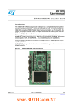
LPC1766-STK development board Users Manual All boards produced by Olimex are ROHS compliant Revision Initial, October 2009 Copyright(c) 2009, OLIMEX Ltd, All rights reserved Page 1 INTRODUCTION: LPC1766-STK is development board with LPC1766 Cortex M3 microcontroller from NXP. This powerful microcontroller supports various serial interfaces such as USB Device/Host/OTG, UART, CAN and other. On the board are avalable audio input and output, digital accelerometer, JTAG, Ethernet, TFT LCD and mini SD/MMC card connector. All this allows you to build a diversity of powerful applications to be used in a wide range of applications. BOARD FEATURES: • MCU: LPC1766 Cortex M3, 100 Mhz, 256KB Flash, 64KB RAM, Ethernet MAC, USB Host/ Device/OTG, x4 UARTS, CAN, SPI, SSP, I2C, I2S, ADC, DAC, TC • LCD NOKIA 6610 128x128 x12bit color TFT with Epson LCD controller • 3-axis digital accelerometer with 11 bit accuracy • temperature sensor • Ethernet 100Mbit • CAN interface and connector • USB host connector • USB device connector • USB OTG connector • two user LEDs • three user buttons • joystick • potentiometer • micro SD/MMC card connector • JTAG and TRACE connectors • power supply • RESET circuit • UEXT connector • Audio IN • Audio OUT • RTC battery • FR-4, 1.5 mm, red soldermask, component print • Dimensions:134.6x101.6mm (5.3 x 4.0") Page 2 ELECTROSTATIC WARNING: The LPC1766-STK board is shipped in protective anti-static packaging. The board must not be subject to high electrostatic potentials. General practice for working with static sensitive devices should be applied when working with this board. BOARD USE REQUIREMENTS: Cables: The cable you will need depends on the programmer/debugger you use. If you use ARM-JTAG-EW, you will need USB A-B cable. If you use a software programmer such as FlashMagic, you will need RS232 cable. Hardware: Programmer/Debugger ARM-JTAG-EW or other compatible programming/debugging tool if you work with EW-ARM. You can use also ARM-USB-OCD, ARM-USB-TINY, ARM-USB-TINY-H with CrossWorks.or OpenOCD. PROCESSOR FEATURES: LPC1766-STK board use ARM 32-bit Cortex™-M3 microcontroller LPC1766FBD100 from NXP Semiconductors with these features: − ARM Cortex-M3 processor, running at frequencies of up to 100 MHz. A Memory Protection Unit (MPU) supporting eight regions is included. − ARM Cortex-M3 built-in Nested Vectored Interrupt Controller (NVIC). − 256 kB on-chip flash programming memory. Enhanced flash memory accelerator enables high-speed 100 MHz operation with zero wait states. − In-System Programming (ISP) and In-Application Programming (IAP) via onchip bootloader software. − On-chip SRAM includes: − 32 kB of SRAM on the CPU with local code/data bus for highperformance CPU access. − Two 16 kB SRAM blocks with separate access paths for higher throughput. These SRAM blocks may be used for Ethernet, USB, and DMA memory, as well as for general purpose CPU instruction and data storage. − Eight channel General Purpose DMA controller (GPDMA) on the AHB multilayer matrix that can be used with the SSP, I2S-bus, UART, the Analog-toDigital and Digital-to-Analog converter peripherals, timer match signals, and for memory-to-memory transfers. − Multilayer AHB matrix interconnect provides a separate bus for each AHB master. AHB masters include the CPU, General Purpose DMA controller, Ethernet MAC, and the USB nterface. This interconnect provides communication with no arbitration delays. Page 3 − Split APB bus allows high throughput with few stalls between the CPU and DMA. − Serial interfaces: − − Ethernet MAC with RMII interface and dedicated DMA controller. − USB 2.0 full-speed device/Host/OTG controller with dedicated DMA controller and on-chip PHY for device, Host, and OTG functions. − Four UARTs with fractional baud rate generation, internal FIFO, DMA support, and RS-485 support. One UART has modem control I/O, and one UART has IrDA support. − CAN 2.0B controller with two channels. − SPI controller with synchronous, serial, full duplex communication and programmable data length. − Two SSP controllers with FIFO and multi-protocol capabilities. The SSP interfaces can be used with the GPDMA controller. − Two I2C-bus interfaces supporting fast mode with a data rate of 400 kbits/s with multiple address recognition and monitor mode. − One I2C-bus interface supporting full I2C-bus specification and fast mode plus with a data rate of 1 Mbit/s with multiple address recognition and monitor mode. − I2S (Inter-IC Sound) interface for digital audio input or output, with fractional rate control. The I2S-bus interface can be used with the GPDMA. The I2S-bus interface supports 3-wire and 4-wire data transmit and receive as well as master clock input/output. Other peripherals: − 70 General Purpose I/O (GPIO) pins with configurable pull-up/down resistors and a new, configurable open-drain operating mode. − 12-bit Analog-to-Digital Converter (ADC) with input multiplexing among eight pins, conversion rates up to 1 MHz, and multiple result registers. The 12-bit ADC can be used with the GPDMA controller. − 10-bit Digital-to-Analog Converter (DAC) with dedicated conversion timer and DMA support. − Four general purpose timers/counters, with a total of eight capture inputs and ten compare outputs. Each timer block has an external count input and DMA support. − One motor control PWM with support for three-phase motor control. − Quadrature encoder interface that can monitor one external quadrature encoder. − One standard PWM/timer block with external count input. − RTC with a separate power domain and dedicated RTC oscillator. The RTC block includes 64 bytes of battery-powered backup registers. − Watchdog Timer (WDT) resets the microcontroller within a reasonable amount of time if it enters an erroneous state. − System tick timer, including an external clock input option. Page 4 − Repetitive interrupt timer provides programmable and repeating timed interrupts. − Each peripheral has its own clock divider for further power savings. − Standard JTAG test/debug interface for compatibility with existing tools. Serial Wire Debug and Serial Wire Trace Port options. − Emulation trace module enables non-intrusive, high-speed real-time tracing of instruction execution. − Integrated PMU (Power Management Unit) automatically adjusts internal regulators to minimize power consumption during Sleep, Deep sleep, Powerdown, and Deep power-down modes. − Four reduced power modes: Sleep, Deep-sleep, Power-down, and Deep powerdown. − Single 3.3 V power supply (2.4 V to 3.6 V). − Four external interrupt inputs configurable as edge/level sensitive. All pins on PORT0 and PORT2 can be used as edge sensitive interrupt sources. − Non-maskable Interrupt (NMI) input. − Clock output function that can reflect the main oscillator clock, IRC clock, RTC clock, CPU clock, and the USB clock. − The Wakeup Interrupt Controller (WIC) allows the CPU to automatically wake up from any priority interrupt that can occur while the clocks are stopped in deep sleep, Power-down, and Deep power-down modes. − Processor wake-up from Power-down mode via interrupts from various peripherals. − Brownout detect with separate threshold for interrupt and forced reset. − Power-On Reset (POR). − Crystal oscillator with an operating range of 1 MHz to 25 MHz. − 4 MHz internal RC oscillator trimmed to 1 % accuracy that can optionally be used as a system clock. − PLL allows CPU operation up to the maximum CPU rate without the need for a high-frequency crystal. May be run from the main oscillator, the internal RC oscillator, or the RTC oscillator. − USB PLL for added flexibility. − Code Read Protection (CRP) with different security levels. Page 5 BLOCK DIAGRAM: Page 6 MEMORY MAP: Page 7 3 .3 V + Page 8 R135 33k + R133 10k ISP 1 30 1 C64 2 .2 u F 22pF 22pF 3 3R 33R 1 00 n F C58 FB0805/120R L6 V BUS DD+ ID GND U SB C67 C66 R 1 22 R1 3 1 100nF DOWN C EN TE R L EFT R IG H T UP R83 33k R82 33k C EN TE R R79 33k 2 1 330R DOWN 3 R85 L EFT DGND 6 5 4 J O YS TICK _ MT5 _ F D<6> Common<5> B<4> R84 R80 33k 330R R IG H T UP 9 8 10 LEDG ND G ND V LE D R81 33k 3 .3 V V DD P L L 1 0 0n F C74 E_ R X_ E R 3 .3V E _ C RS E_ MD IO E_ MD C R127 R128 E_ R X D1 E_ R XD 0 3 .3 V NA 3 .3 V OUT L5 C21 1 0 uF/6 .3 V 10 0 n F + 2 100nF C8 2 3 .3 V L ED 2 AC C _ IR Q /L ED 2 R89 1 x3 56 0 R 56 0 R C47 100nF R 52 B U T1 T1 15 7 R11 33k 3 .3 V MO S I1 ,MISO 1,S C K1 ,SS EL 1 BU T1 USER BUTTONS 1.5k/1% C 79 330R R107 100nF 2 .5 V 100nF 330R R96 NA R97 R98 1k PC _ C D PC _ R XD PC _ TXD P C _ DTR D B9 -F 6 7 8 9 G2 PC _ D SR PC _ R TS P C _ CTS 1 3 2 AG AY R130 3 .3k 3 .3V 7 6 8 L ED AC T K Y 1nF/2kV YELLOW GREEN L AN B U T2 T1 1 5 7 R20 33k 3 .3 V AG N D AN _ TR IM 10k 3 .3 VA 75 75 75 75 DS R 1 RXD0 D TR 1 TXD 0 3 7 8 6 1 4 5 2 3 30 R R37 3 R35 330R R23 3 30 R 12 9 11 10 5 C51 4 1 00 n F C 50 1 10 0 n F 3 .3 V GND15 R1IN R2IN T 1OUT T2O UT V- V+ AO U T M IC _ IN C 40 13 8 14 7 6 2 C53 100nF C52 1 0 0 nF 100nF C33 R5 6 R111 R112 L2 R113 R117 Z2 BZV5 5 C 2 V4 Z1 B ZV 5 5 C2 V 4 R60 1 00 R C44 1 0 0 nF 6 1uF C38 C 45 U5 L M 38 6 47nF 5 VA C 42 10R AG N D 1 0 0 u F/1 6 V R64 + 4 7u F/6 .3 V C43 C39 2 3 6 4 5 7 8 1 P 1 .2 9 P 1 .28 R 11 4 3 3k 3 .3 V R 12 1k ISP_ E 1x2 1-L 2 3-R MIC R10 33k JA CK -S MD -3 .5 mm 1-L 2 3-R H EA DP H O N E JA CK -S MD -3 .5 mm R 21 NA T2 B C 81 7 3 .3 V MIC R O _ SD /M MC CD/DA T 3/CS CMD/DI VSS V DD CLK /S CLK DA T 0/DO DA T1/RE S DA T2/RES SD /MM C B H 1 0S B H 10 S BH 1 0 S BH 1 0 S BH 1 0 S BH 1 0 S B H 10 S B H1 0 S BH 1 0 S BH 1 0 S 4 7 u F/6 .3V AG N D AGND AGND 47pF C28 C24 1 00 n F R3 10k R57 560R D4 1N4148 R9 33k P1 .2 9 P 1 .28 R E SET D3 1N4148 AG N D C41 AGND R2 100k R1 1 00 k 3 .3 VA 100nF C20 3 .3 V 6 7 8 9 G2 G1 SC K1 MISO 1 S SE L1 M O SI1 R S2 3 2 _ 0 DB 9 -F 1 2 3 4 5 R8 33k 8 AG N D 5 100nF AG N D AG N D AG N D 2 3 AGND 2 3 T1 B C 81 7 5 VA 5V A M C P6 0 1 R58 470k R59 100k 3 .3 V R ST_ E 1 x2 AG N D U9 100nF C 30 D2 1N4148 R7 33k AG N D R66 1k C 59 MISO 1 4 7 u F/6 .3 V 33 k 33k 33k MM C _P W R U X T-1 U XT- 2 U XT- 3 U XT-4 U XT-5 UX T-6 U X T- 7 U XT- 8 U XT- 9 U XT-1 0 UXT TXD3 RXD3 SCL2 SDA2 MISO1 MOSI1 SCK1 CS_UEXT 3 .3 V SD/MMC S SE L1 M O SI1 1k R33 4 7 0 nH 33k NA R S TN ISP _ E R6 5 33k C25 47pF AUDIO PC _ D TR P C_ D S R AGND 47pF S T3 2 3 2 (S O 1 6 ) R1O UT R2O UT T1IN T2IN C2- C2+ C1- C57 100nF U 6 PW R 16VCC C1+ U6 SD R32 560R C56 33k R34 1 0 0 nF( N A) T4 IR LM 6 4 0 2 3 .3V RE D(GY X -S D-TC0805S URK) R116 2k AG N D R1 5 10 k TH 1 TH ER M ISTO R 1 0 u F/6 .3 V( NA ) C16 AG N D RS232 56 0 R C23 100nF R 76 1k R6 R JL B C- 0 6 0TC 1 1:1 1:1 1 0 0 nF C80 BU T2 AIN 5 TD+ COM TDAG KG AY KY RD+ NC RD- R 1 06 4 9.9 /1 % L E D1 0 0 K G 2 .5 V PH Y _IN T NA C8 9 3 POTENTIOMETER G1 R S 23 2 _ 1 1 2 3 4 5 1 EXT_ TEM P/TH 1 EX T_ TE MP TE MP 3 .3 VA TEMPERATURE SENSOR EX T_ TE MP ETHERNET 2 .5 V 3 .3 V 3 .3 V NA R 87 33 0 R R101 C76 3.3 V 36 35 34 33 32 31 30 29 28 27 26 25 R104 4 .9 9 k/1 % R126 C48 1 0 u F/6 .3V 2 .5 V PC _ TXD P C _ RTS 3 .3 V P C_ R X D PC _ C TS 13 8 C63 100nF C62 1 0 0 nF 14 7 6 2 MDIO GND5 MDC GND4 RX D3/P HY A D1 F X S D/FX E N RX D2/P HY A D2 RX + RX D1/P HY A D3 RX RX D0/P HYA D4 V DDRX VDDIO1 P D# G ND1 LE D3/NW A Y EN RX DV /CRS DV /P CS _LP BK LE D2/DUP LE X RX C LE D1/S P D100/NFE F RX ER/IS O LE D0/TE S T GND2 INT /P HY A D0 L4 10k R1 9 FB0805/120R 1 2 3 4 5 6 7 8 9 10 11 12 C7 5 3 .3 k 3 .3 k VS S 6 N C 2 -5 0 MH z C8 1 FB0805/120R 100nF V D DP L L + C49 R STO U TN 1 0 u F/6.3 V U4 K S8 7 2 1 BL R17 V DD CD 1 4 3 .3 k 3 .3 k 1k 100k R120 R16 C<3> E<2> Center push A<1> J1 3 .3 V JOYSTICK Q4 BC 8 1 7 0 N O K IA6 6 1 0 _ CO L O R _ L C D BL _ PW R R74 RE S ET E _ CR S R 1 23 1k E /D R1IN R2IN T 1OUT T2O UT V- V+ C65 100nF LE D 2 3 .3 V TXD 1 ,R XD 1 ,R TS1 ,C TS1 ,D TR 1,D S R 1,D C D 1 ,TXD 0 ,R XD 0 S T3 2 3 2 (S O 1 6 ) R1O UT R2O UT T1IN T2IN C2- C2+ C1- C1+ GND15 W AKE -U P U 1 1 PW R 16VCC R41 33k CAN TB 3 -3 .5 mm 3 2 1 RE D(GY X -S D-TC0805S URK ) AC C _ IR Q L ED 2 /AC C _ IR Q 24 23 22 21 1k 20 1k 19 18 17 E _T XD 1 16 E _T XD 0 15 E_ T X _ EN 14E_ R EF_ CL K 13 100nF 18 17 16 15 14 13 C69 US B_ O TG M IC RO _ AB GND2 GND1 ID A GND DP DM DA T /V P S E 0/V M C68 100nF USB_OTG 330R C22 1 0u F/6 .3 V R73 2 L C D _ RS T S CK DIO CS V DIS P LA Y V DIG ITA L LCD 3 1 5 12 9 11 10 R124 R 1 25 R1 2 1 R18 R 78 NA R14 330R 8 7 6 5 VDDIO2 GND3 CRS/RMII_BTB COL/RMII TXD3 TXD2 TXD1 TXD0 TXEN TXC/REFCLK TXER VDDC V RE G3V 3 S US P END OE _N/INT_N VM VP RCV 10uF/6.3V C72 C70 1 00 n F 10uF/6.3V 7 4 7 8 9 10 11 12 24 23 22 21 20 19 R72 2k 1k NA + C71 V CC(I/O ) CG ND C2 C1 V CC V B US R71 R 75 4 3 5 6 1 SC K0 M ISO 0 S SEL 0 3 C60 4 1 00 n F R 1 46 3 30 R RS CA NH CA NL V RE F O P EN R38 120R USER LEDS 3 .3 V U11 56 0 R C73 100nF R 11 5 C 54 1 10 0 n F 3 .3 V 1 0k 2 RE D(GY X -S D-TC0805S URK ) LE D 1 R90 56 0 R 3 .3 V TX D VSS V DD RX D U7 MC P2 5 5 1 1 2 3 4 1 C A N_ D R 40 REXT VDDRCV GND6 TXTX+ VDDTX GND7 GND8 XO XI VDDPLL RST# A DR/P S W S DA S CL RE S E T_N INT _N S PE E D 3 .3 V R 68 1 .2k /1 % R108 33k E_ R EF_ C L K E_ R XD 0 E_ R XD 1 E_ R X_ ER 2.2k R132 33k U8 4 L C D _ BL 5 R69 5 .6 k/1 % 3 .3V 0R +5 V CAN LED100 1 US B _S DA 2 US B _S CL 3 4 RS TO UTN #E INT 1 5 6 S H IE L D U SB _ A MC 3 4 0 6 3 FB SC SE 1 2 1 50 R U3 TC D5 1 N 5 8 19 S + R137 2k L3 FB0805/120R C10 3 L1 220uH R70 R6 7 2 .2 NOKIA LCD BL _ PW R 3 .3V DCD1 RX D 1 C TS 1 TXD 1 R TS1 C55 R5 100nF 0 R (N A) W AK E- UP L ED 1 RD1 TD 1 R22 4 .7 k( N A) 3.3 V 37 38 39 40 41 42 43 44 45 46 47 48 R136 2k R 93 15k 1 2 3 4 US B_ H O S T +5V 220uF/16V/MINI C46 3 .3 V R 94 15k H O ST_ PW R S H IE L D U SB_ B V CC 2 R13 4 .7 k( N A) 3.3 V + R103 10k C 78 33R 33R V BU S GND 10 0 n F(N A ) C84 1 RE S E T E_ TX D0 E_ TXD 1 E_ TX_ EN E _ C RS E _ RX D 0 E_ R X D1 E_ R X_ E R E_ R EF_ C L K E_ MD C E _ MD IO R TS1 TXD 1 R XD 1 C TS1 D CD 1 DSR1 D TR 1 S SEL 1 SC K 1 MIS O 1 MO S I1 RD1 TD 1 TXD 0 R XD 0 3 .3V 3 .3 V R100 1 6 U S B_ O TG _D U S B_ O TG _ D + RSTN,RTCK,TCK,TRSTN,TMS,TDI,TDO R134 10k C 77 C61 10nF 1 2 3 4 U SB _ DE V R STN R140 U1 0 N A MC P1 3 0 T(N A) 3 .3 V RESET CIRCUIT 4 .7 k R86 SD A2 R105 R99 3 .3 V + 4 7 p F(N A) 4 7 p F(N A) 0 R ( N A) +5V _ U SB_ D E V DD+ 0R 3 .3 V 4 .7 k R77 S CL 2 R95 + U S B_ SD A U S B_ SC L 100nF R92 R91 R39 USB_HOST R30 560R USB 3 .3 V 3 .3 V 3 .3V D- D+ R27 1 .5 k/1 % UP DOW N TR AC E_ D 3 TRA C E_ D 2 TR A C E_ D 1 TR A CE _ D 0 TR AC E _ CL K L EFT R IG H T U SBD _ C O N N EC T IS P_ E # E INT1 W A KE -U P BU T2 VSS 10k 10k 1 0k L M 35 2 6 M -L (S O 8 ) 0R 0 R (N A ) USB_HOST_DUSB_HOST_D+ R36 100k 18pF R2 4 33R R26 C 32 33R USB_DEVICE U S BC G R E EN (G YX -SD - TC0 8 0 5 SG C ) R129 100k + R138 R154 R 15 2 C 1 12 8 7 6 5 H O ST_ PW R +5 V U S BH _ PW RD 18pF C 31 2 .2 k R29 T3 B C 8 07 3 .3 V 75 74 73 70 69 68 67 66 65 64 53 52 51 50 UP DOW N TR AC E_ D 3 TRA C E_ D 2 TR A C E_ D 1 TR A CE _ D 0 TR AC E _ CL K L EFT R IG H T U SBD _ C O N N EC T IS P_ E # E INT1 W A KE -U P BU T2 75 74 73 70 69 68 67 66 65 64 53 52 51 50 SD A2 S CL 2 A C C_ IR Q R139 0 R (N A) 4 H N 2 x3 U SB _ DE V_ D - U S B_ D EV _D + U SB D _ CO N NE C T R28 10k R2 5 R31 560R 3 .3 V L PC 1 7 66 FB D1 0 0 P 3[25]/MA T 0[0]/P WM1[2] P 3[26]/S TCLK /MA T0[1]/P W M1[3] P 4[28]/RX _MCLK /MA T 2[0]/TX D3 P 4[29]/TX _MCLK /MA T2[1]/RX D3 P 2[0]/P W M1[1]/T X D1 P 2[1]/P WM1[2]/RX D1 P 2[2]/P WM1[3]/CTS 1/T RA CEDA T A [3] P 2[3]/P WM1[4]/DCD1/TRA CE DA TA [2] P2[4]/P WM1[5]/DS R1/TRA CE DA T A [1] P 2[5]/PW M1[6]/DT R1/TRA CE DA TA [0] P 2[6]/P CA P 1[0]/RI1/TRA CE CLK P 2[7]/RD2/RT S 1 P 2[8]/TD2/TX D2 P 2[9]/US B_CO NNE CT /RX D2 P2[10]/#E INT0/NMI P 2[11]/#E INT1/I2S TX _CLK P 2[12]/#E INT 2/I2S T X _WS P 2[13]/#E INT 3/I2S T X _S DA VCC #E NA O UT_A FLA G _A IN FLA G _B GND #E NB OUT_B U1 3 U SB _ LIN K YEL L O W (G YX- SD -TC 0 8 0 5 SYC ) U SB_ U P _ LE D 3 .3 V 27 26 82 85 #RS T OUT #RE S E T RT CK TCK /S WDCLK #TRS T TMS /S WDIO T DI T DO/S W O X T AL2 C11 DC IS US B_ H O S T_D U S B_ H O ST_ D + 1 2 3 4 L C D _ RS T L C D _B L TXD 3 R XD 3 23 14 17 100 5 4 3 2 1 6 8 7 U SB_ D EV _ D US B_ H O S T_D U S B_ O TG _ D - # U SB _ PPW R # U SB _ O VR C R 27 26 82 85 R STO U TN R S TN R TC K TC K TR STN TMS TD I TD O TR AC E _ CL K ,TRA C E_ D [0 ..3] R STO U TN R S TN R TC K TC K TR STN TMS TD I TD O E_ TX D0 E_ TXD 1 E_ TX_ EN E _ C RS E _ RX D 0 E_ R X D1 E_ R X_ E R E_ R EF_ C L K E_ MD C E _ MD IO U SB _ U P_ L ED # U SB _P PW R SC K0 SSE L 0 U S BH _ PW RD M ISO 0 R151 1k MO SI0 L ED 1 C S_ U EXT #U S B_ O V R CR P 1 .28 P 1.2 9 VB U S C 8 3 1 0 0 nF AIN 5 AGND U SB _ DE V_ D + U SB_ H O ST_ D + U SB_ O TG _ D + 14 17 100 5 4 3 2 1 X TA L1 10 0 n F R8 8 330R AGND 2 4 6 R51 10k D BG _ E TR S TN TD I TMS TC K R TC K TD O R S TN 22 RTCX 2 RT CX 1 95 94 93 92 91 90 89 88 87 86 32 33 34 35 36 37 38 39 40 43 44 45 21 20 E_ TX D0 E_ TXD 1 E_ TX_ EN E _ C RS E _ RX D 0 E_ R X D1 E_ R X_ E R E_ R EF_ C L K E_ MD C E _ MD IO U SB _ U P_ L ED # U SB _P PW R SC K0 SSE L 0 U S BH _ PW RD M ISO 0 MO SI0 L ED 1 C S_ U EXT #U S B_ O V R CR P 1 .28 P 1.2 9 VB U S AIN 5 95 94 93 92 91 90 89 88 87 86 32 33 34 35 36 37 38 39 40 43 44 45 21 20 RD1 TD 1 TXD 0 R XD 0 L ED 2 /AC C _ IRQ C E N TE R S SEL 1 SC K 1 MIS O 1 MO S I1 SD A2 S C L2 TXD 1 R XD 1 C TS1 D CD 1 DSR1 D TR 1 MM C _ PW R R TS1 BU T1 C1 7 TEMP M IC _IN AOUT U SB _ SD A U SB _S C L U SB_ D + U S B_ D - SMB 3 8 0( Q FN 1 0 ) 4 5 0R 3 LEDACT NA 49.9/1% U SB _D - 2 4 6 R50 10k 2 1 R46 10k 23 22 18 16 P 1[0]/E NE T_TX D0 P 1[1]/E NE T_TX D1 P 1[4]/E NET _TX _E N P 1[8]/ENE T _CRS P 1[9]/E NE T_RX D0 P 1[10]/E NE T_RX D1 P 1[14]/E NE T_RX _E R P 1[15]/E NET _RE F_CLK P1[16]/ENE T _MDC P 1[17]/E NE T_MDIO P 1[18]/US B _UP _LE D/P WM1[1]/CA P 1[0] P 1[19]/MC0A /#US B _P P WR/CA P 1[1] P 1[20]/MCF B0/P WM1[2]/S CK 0 P 1[21]/MCA B ORT/P WM1[3]/S SE L0 P 1[22]/MC0B /US B _P WRD/MAT 1[0] P 1[23]/MCFB 1/P W M1[4]/MIS O0 P 1[24]/MCF B 2/P WM1[5]/MO S I0 P 1[25]/MC1A /MA T1[1] P 1[26]/MC1B /P W M1[6]/CA P 0[0] P 1[27]/CLK O UT/#US B _OV RCR/CA P 0[1] P 1[28]/MC2A/P CA P1[0]/MA T0[0] P 1[29]/MC2B /P CAP 1[1]/MA T0[1] P 1[30]/V B US /A D0[4] P 1[31]/S CK 1/A D0[5] 46 47 98 99 81 80 79 78 77 76 48 49 62 63 61 60 59 58 57 56 9 8 7 6 25 24 29 30 RD1 TD 1 TXD 0 R XD 0 L ED 2 /AC C _ IRQ C E N TE R S SEL 1 SC K 1 MIS O 1 MO S I1 SD A2 S C L2 TXD 1 R XD 1 C TS1 D CD 1 DSR1 D TR 1 MM C _ PW R R TS1 BU T1 TEMP M IC _IN AOUT U SB _ SD A U SB _S C L U SB_ D + U S B_ D - 46 47 98 99 81 80 79 78 77 76 48 49 62 63 61 60 59 58 57 56 9 8 7 6 25 24 29 30 U SB 49.9/1% 49.9/1% H N 2 x3 U SB _ D+ R110 10k R47 10k USB R109 10k R48 10k Q1 C13 12.000MHz/20pF 33pF 16 Q2 3 2 7 6 8 /6p F 18 V SS VS S VSS VSS P 0[0]/RD1/TX D3/S DA 1 P 0[1]/T D1/RX D3/S CL1 P 0[2]/T XD0/A D0[7] P 0[3]/RX D0/A D0[6] P 0[4]/I2S RX _CLK/RD2/CA P 2[0] P 0[5]/I2S RX _WS /T D2/CA P 2[1] P 0[6]/I2S RX_S DA /SS E L1/MA T2[0] P 0[7]/I2S TX _CLK/S CK 1/MA T 2[1] P 0[8]/I2S T X _WS /MIS O1/MA T2[2] P 0[9]/I2S T X_S DA /MOS I1/MA T 2[3] P0[10]/TX D2/S DA 2/MA T3[0] P 0[11]/RX D2/S CL2/MA T3[1] P 0[15]/T X D1/S CK 0/S CK P 0[16]/RX D1/S S E L0/S S E L P 0[17]/CTS 1/MIS O 0/MIS O P 0[18]/DCD1/MOS I0/MOS I P0[19]/DS R1/SDA 1 P 0[20]/DT R1/S CL1 P 0[21]/RI1/RD1 P 0[22]/RTS 1/TD1 P 0[23]/A D0[0]/I2S RX _CLK/CA P 3[0] P 0[24]/A D0[1]/I2S RX _WS /CA P 3[1] P 0[25]/A D0[2]/I2S RX _S DA /TX D3 P 0[26]/A D0[3]/A O UT /RX D3 P 0[27]/S DA 0/US B _S DA P 0[28]/S CL0/US B _S CL P 0[29]/US B_D+ P0[30]/US B _D- AG ND AGND 100nF 100nF 3 9 2 6 7 8 ACCELEROMETER NC1 S CK NC2 S DO S DI/SDA VDDIO V DD INT GND CS B U2 SCK0,MISO0,SSEL0,LCD_RESET,LCD_BL 7 1 3 5 R49 10k 1 3 5 7 9 11 13 15 17 19 +5V_JLINK 0R 1 2 + U SB_ D - 0R C12 G ND 72 55 31 1 0 0 n F 97 C6 V DD(3V 3) VDD(3V 3) V DD(3V 3) V DD(3V 3) V SS VSS 2 CLOSE 1 AG N D _ E C29 100nF C19 C34 1 10 + 6x3.8x2.5(SMD) 1 3 5 R150 33pF C15 100nF 97 72 55 31 28 54 71 96 83 41 V RE G(3V 3) V RE G(3V 3) 2 C L O SE 1 3 .3 V A_ E 3 .3 V SCL2,SDA2 1 2 U SB _ D+ 0R(NA) R53 JTA G 0R(NA) 2 4 6 8 10 12 14 16 18 20 3 .3 V 20pF C1 4 100nF 1 0 0 nF C2 42 84 VSSA V DDA 47uF/6.3V 20 p F C4 100nF 2 C3 28 54 71 96 C5 83 41 10 1 0 0 n F 11 C7 AG ND V RE FN V RE F P VBAT NC + JTAG R 1 5 7 TD O R 1 6 1 TR STN 10uF/6.3V C8 12 19 13 1 0 0 n F 15 C9 C 26 3 .3 V_ E C LO SE 3 .3 VA 1 2 3 TRA C E_ D 3 TR A C E_ D 2 TR AC E _ D1 TR AC E _D 0 TR AC E_ C L K NA NA C1 1 0 0 nF 3.3 V (I/O ) _ E CLOSE 1 TR AC E _ CL K - AG N D 3.3 V (V RE G ) _E 4 2 1 2 84 CLOSE + TMS TC K TD O TDI R S TN 3V_BAT 2 4 6 8 10 12 14 16 18 20 + 11 10 15 19 3 .3 VA + TRA C E FTS H -1 1 0 -0 1 -L - D V BA T _ H OL D ER 3 .3 V 12 U1 PW R R55 330R R4 2 4 0R /1 % R54 3 9 0 R/1 % A DJ/G ND O UT 3 .3 V 1 1 3 5 7 9 11 13 15 17 19 1 2 D1 B AT5 4 C C18 100nF IN VR 1 (3 .3 V) L M 1 1 17 3 .3 V CLOSE CAN_T W F2 S B AT 10uF/6.3V h ttp://w w w .o lime x.c o m/d e v 3 .3 V C37 C LO SE 5V A 1 C O P YR IG H T(C ) , 2 00 9 5-6 - +5V_USB 3-4 - +5V_JLINK 1-2 - +5V_EXT 5 3 1 + R e v . In itia l LPC1766-STK 4 7 u F/6.3 V C35 6 4 2 2 2 R 63 3 3 0 R /1 % C27 100nF R61 2 2 0R /1 % R62 3 3 0 R /1% A DJ/G ND +5V_USB_DEV +5V_JLINK +5V_EXT 1 5 VA _ E + GND C3 6 4 7 0 u F/1 6 VD C O UT +5V 2 DEBUG INTERFACE: TRACE 6 VAC 9V D C IN VR 2 (5 V ) LM 1 1 17 P W R _ SEL 2 x3 POWER SUPPLY 2 P W R _ JA CK D B1 0 4 (S MD ) G1 VIN SCHEMATIC: RJ45 SIDE E_TXD[0..1],E_TX_EN,E_CRS,E_RXD[0..1],E_RX_ER,E_REF_CLK,E_MDC,E_MDIO R102 470pF UP,DOW N,LEFT,RIGHT GND4 GND3 25 BOARD LAYOUT: POWER SUPPLY CIRCUIT: LPC1766-STK is typically power supplied with 9 VDC. The programmed board power consumption is about 200 mA with all peripherials enabled Page 9 RESET CIRCUIT: LPC1766-STK reset circuit includes jumper RST_E, pin 15 of JTAG connector, pin 10 of TRACE connector and RESET button. CLOCK CIRCUIT: Quartz crystal 12 MHz is connected to LPC1766 pin 22 (XTAL1) and pin 23 (XTAL2). Quartz crystal 32.768 kHz is connected to LPC1766 pin 16 (RTCX1) and pin 18 (RTCX2). JUMPER DESCRIPTION: CAN_D CAN Disable. If this jumper is closed, the CAN is disabled. Default state is open. CAN_T This jumper assures correct work of the CAN. At each end of the bus it should be closed. This means that if you have only two devices with CAN, the jumpers of both devices should be closed. If you have more than two devices, only the two end-devices should be closed. Default state is closed. 3.3V(VREG)_E This jumper, when closed, supplies 3.3 V voltage for the on-chip voltage regulator only – 42 and 84 pins of the MCU. Default state is closed. 3.3V_E This jumper, when closed, enable the main 3.3 V regulator VR1(3.3V) - LM1117. Default state is closed. 3.3VA_E This jumper, when closed, supplies 3.3 V voltage to the VDDA and VREFP pins of the MCU. Default state is closed. 3.3V(I/O)_E This jumper, when closed, supplies 3.3 V voltage to the VDD – 4 pins of the MCU. Default state is closed. Page 10 5VA_E This jumper, when closed, supplies analog 5V voltage supply to the audio amplifiers. Default state is closed. AGND_E This jumper, when closed, connects analog GND to the GND of the MCU. Default state is closed. EXT_TEMP/TH1 This jumper, when is in position EXT_TEMP – takes signal from external temperature sensor and when is in position TH1 – takes signal from the thermistor TH1 of the board. Default state is in position TH1. DBG_E The position of this jumper doesn’t matter. Default state is closed. RST_E This jumper, when closed, enables programing via RS232. Default state is open. ISP_E This jumper, when closed, enables programing via RS232. Default state is open. ACC_IRQ/LED2 This jumper when is in position ACC_IRQ – enables interrupt request from the accelerometer and when is in position LED2 – enables LED2. Default state is LED2. USB_D- This jumper, when1-2 are shorted – enables USB DEVICE, when 3-4 are shorted– enables USB HOST and when 5-6 are shorted – enables USB OTG. Default state is 1-2. Page 11 USB_D+ This jumper, when1-2 are shorted – enables USB DEVICE, when 3-4 are shorted– enables USB HOST and when 5-6 are shorted – enables USB OTG. Default state is 1-2. PWR_SEL When 1-2 are shorted – the board is supplied from PWR_JACK, when 3-4 are shorted – the board is supplied from JTAG and when 5-6 are shorted – the board is supplied from USB_DEV. Default state is 1-2. INPUT/OUTPUT: LED1 (red) connected to LPC1766 pin 39 (P1[25]/MC1A/MAT1[1]). LED2 (red) connected to LPC1766 pin 81 (P0[4]/I2SRX_CLK/RD2/CAP2[0]) via jumper ACC_IRQ/LED2, when this jumper is in position LED2. SD/MMC LED (red) connected to SD/MMC pin 4 (VDD). Power-on LED (red) with name PWR – this LED shows that +3.3V is applied to the board. USB_UP_LED with name USB_LINK (yellow) connected to LPC1766 pin 32 (P1[18]/USB_UP_LED/PWM1[1]/CAP1[0]). USBD_CONNECT LED with name USBC(green) connected to LPC1766 pin 64 (P2[9]/USB_CONNECT/RXD2) through T3 and R29. User button with name BUT1 connected to LPC1766 pin 9 (P0[23]/AD0[0]/I2SRX_CLK/CAP3[0]). User button with name BUT2 connected to LPC1766 pin 50 (P2[13]/#EINT3/I2STX_SDA). User button with name WAKE-UP connected to LPC1766 pin 51 (P2[12]/#EINT2/I2STX_WS). User button with name RESET connected to LPC1766 pin 17 (#RESET). Joystick button with name J1 this is 4 directions plus center button, in the schematic the joystick four directions switches are connected through 33k resistors to LPC1766 pins - 65 (P2[8]/TD2/TXD2) – RIGHT, 66 (P2[7]/RD2/RTS1) – LEFT, 74 (P2[1]/PWM1[2]/RXD1) – DOWN, 75 (P2[0]/PWM1[1]/TXD1) – UP, the center button is connected to pin 80 (P0[5]/I2SRX_WS/TD2/CAP2[1]). Trimpot with name AN_TRIM connected to LPC1766 pin 20 (P1[31]/SCK1/AD0[5]). TFT LCD - 128x128 12 bit color with backlight. Page 12 EXTERNAL CONNECTORS DESCRIPTION: RS232_0: Pin # Signal Name 1 NC 2 T2OUT 3 R2IN 4 RST_E 5 GND 6 NC 7 ISP_E 8 NC 9 NC RS232_1: Pin # Signal Name 1 PC_CD 2 PC_RXD 3 PC_TXD 4 PC_DTR 5 GND 6 PC_DSR 7 PC_RTS 8 PC_CTS 9 NC Page 13 PWR_JACK: Pin # Signal Name 1 Power Input 2 GND UXT: Pin # Signal Name 1 3.3V 2 GND 3 TXD3 4 RXD3 5 SCL2 6 SDA2 7 MISO1 8 MOSI1 9 SCK1 10 CS_UEXT JTAG: The JTAG connector allows the software debugger to talk via a JTAG (Joint Test Action Group) port directly to the core. Instructions may be inserted and executed by the core thus allowing LPC1766 memory to be programmed with code and executed step by step by the host software. For more details refer to IEEE Standard 1149.1 - 1990 Standard Test Access Port and Boundary Scan Architecture and LPC1766 datasheets and users manual. Page 14 Pin # Signal Name Pin # Signal Name 1 3.3V 2 3.3V 3 TRSTN 4 GND 5 TDI 6 GND 7 TMS 8 GND 9 TCK 10 GND 11 RTCK 12 GND 13 TDO 14 GND 15 RSTN 16 GND 17 through 10K to GND 18 GND 19 +5V_JLINK 20 GND LAN: Page 15 Pin # Signal Name Chip Side Pin # Signal Name Chip Side 1 TPOUT+ 5 Not Connected (NC) 2 TPOUT- 6 Not Connected (NC) 3 2.5V 7 TPIN+ 4 Not Connected (NC) 8 TPIN- LED Color Usage Right Yellow Activity Left Green 100MBits/s (Half/Full duplex) CAN Pin# Signal Description 1 GND Ground 2 CANL CAN LOW 3 CANH CAN HIGH TRACE Pin# Signal Description Pin# Signal 1 VCC 3,3V 2 TMS 3 GND 4 TCK 5 GND 6 TDO 7 NC 8 TDI 9 GND 10 RSTN 11 GND 12 TRACE_CLK 13 GND 14 TRACE_D0/TDO Depends on R150/R157 15 GND 16 TRACE_D1/TRST Depends on R153/R161 17 GND 18 TRACE_D2 19 GND 20 TRACE_D3 Page 16 Description Page 17 USB_HOST Pin # Signal Name 1 HOST_PWR 2 USB_HOST_D- 3 USB_HOST_D+ 4 GND USB 2.0 full-speed Host controller with dedicated DMA controller and on-chip PHY. The host controller enables full- and low-speed data exchange with USB devices attached to the bus. It consists of a register interface, a serial interface engine, and a DMA controller. The register interface complies with the OHCI specification. USB_DEVICE Pin # Signal Name 1 +5V_USB_DEV 2 USB_DEV_D- 3 USB_DEV_D+ 4 GND The device controller enables 12 Mbit/s data exchange with a USB Host controller. It consists of a register interface, serial interface engine, endpoint buffer memory, and a DMA controller. The serial interface engine decodes the USB data stream and writes data to the appropriate endpoint buffer. The status of a completed USB transfer or error condition is indicated via status registers. An interrupt is also generated if enabled. When enabled, the DMA controller transfers data between the endpoint buffer and the on-chip SRAM. Page 18 USB_OTG Pin # Signal Name 1 VBUS 2 USB_OTG_D- 3 USB_OTG_D+ 4 USB_OTG_ID 5 GND USB OTG is a supplement to the USB 2.0 specification that augments the capability of existing mobile devices and USB peripherals by adding host functionality for connection to USB peripherals. The OTG Controller integrates the host controller, device controller, and a master-only I2Cbus interface to implement OTG dual-role device functionality. The dedicated I2C-bus interface controls an external OTG transceiver. BAT Pin # Signal Name 1 to 3.3V 2 GND MIC Pin # Signal Name 1 AGND 2 NC 3 MIC Page 19 HEADPHONE Pin # Signal Name 1 AGND 2 IN1=IN2 3 IN2=IN1 SD/MMC Pin # Signal Name 1 Pull-up 2 SSEL1 3 MOSI1 4 VDD (power supply) 5 SCK1 6 GND 7 MISO1 8 Pull-up 9 Not connected 10 Not connected 11 Not connected 12 Not connected Page 20 MECHANICAL DIMENSIONS: All measures are in Inches. Page 21 AVAILABLE DEMO SOFTWARE: Accelerometer Demo - Basic use of I/O, timer, interrupt controllers, LDC module and the on board accelerometer EW-ARM 5.40. Audio Device Class - USB audio device class with one output and one input EW-ARM 5.40. Getting Started - Basic use of I/O, timer and interrupt controllers EW-ARM 5.40. LCD Demo - Basic use of the I/O, timer, interrupt controllers and LDC module for graphic and text drawing EW-ARM 5.40. Mass Storage Class - USB mass storage class with MMC/SD card drive EW-ARM 5.40. Simple periherals - Simple ADC demo, Basic use of ADC, Simple DAC demo, Basic use of DAC, Simple DMA demo, Basic use of DMA, Simple EMAC demo, Basic use of EMAC, Simple EXTINT demo, Basic use of EXTINT, Simple GPIO demo, Basic use of GPIO, Simple RTC demo, Basic use of RTC, Simple SSP demo, Basic use of SSP, Simple Timer demo, Basic use of Timer, Simple UART demo, Basic use of UART, Simple WDT demo, Basic use of WDT EW-ARM 5.40. uIP WEB Server - WEB server application running on the top of the uIP 1.0 TCP-IP stack EW-ARM 5.40. USB Host Demo - USB host masstorage class framework EW-ARM 5.40. USB Mouse - USB HID class (Mouse) EW-ARM 5.40. Virtual COM Port - USB communication device class EW-ARM 5.40. Page 22 ORDER CODE: LPC-1766STK - assembled and tested board How to order? You can order to us directly or by any of our distributors. Check our web www.olimex.com/dev for more info. Revision history: Revision Initial, October 2009 Page 23 Disclaimer: © 2009 Olimex Ltd. All rights reserved. Olimex®, logo and combinations thereof, are registered trademarks of Olimex Ltd. Other terms and product names may be trademarks of others. The information in this document is provided in connection with Olimex products. No license, express or implied or otherwise, to any intellectual property right is granted by this document or in connection with the sale of Olimex products. Neither the whole nor any part of the information contained in or the product described in this document may be adapted or reproduced in any material from except with the prior written permission of the copyright holder. The product described in this document is subject to continuous development and improvements. All particulars of the product and its use contained in this document are given by OLIMEX in good faith. However all warranties implied or expressed including but not limited to implied warranties of merchantability or fitness for purpose are excluded. This document is intended only to assist the reader in the use of the product. OLIMEX Ltd. shall not be liable for any loss or damage arising from the use of any information in this document or any error or omission in such information or any incorrect use of the product. Page 24