1
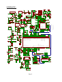
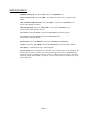
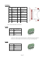
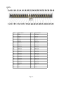
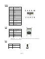
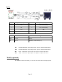
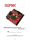
LPC-2378STK development board
Users Manual
Rev. C, July 2009
Copyright(c) 2009, OLIMEX Ltd, All rights reserved
Page 1
INTRODUCTION:
LPC-2378STK is a starter kit which uses Microcontroller LPC2378 from NXP. This
microcontroller supports various serial interfaces such as USB 2.0, UART, CAN, etc.
In addition you will find also audio input and output, JTAG, Ethernet, TFT display
and SD/MMC card holder on this board. All this along allow you to build a diversity
of powerful applications to be used in a wide range of situations.
BOARD FEATURES:
−
−
−
−
−
−
−
−
−
−
−
−
−
−
−
−
−
−
−
−
−
−
−
−
−
MCU: LPC2378 16/32 bit ARM7TDMI-S™t with 512K Bytes Program Flash, 16K
Bytes RAM, EXTERNAL MEMORY BUS, RTC, 4x 10 bit ADC 2.44 uS, 2x UARTs,
4x CAN, I2C, SPI, 2x 32bit TIMERS, 7x CCR, 6x PWM, WDT, 5V tolerant I/O, up
to 60MHz operation
standard
JTAG
connector
with
ARM
2x10
pin
layout
for
programming/debugging with ARM-JTAG
Optional - TRACE connector
128x128 pixel 12 bit color TFT LCD with backlight
Ethernet 100MBit
MMA7620 3 axis accelerometer
Two RS232 port
Two CAN drivers and connector
SD/MMC card connector
UEXT connector with I2C, SPI, RS232 and power supply for connecting add-on
modules like RF link, MP3, etc available from Olimex
IrDA transceiver on board
Audio in and Audio Out jacks for microphone and headphones
trimpot connected to ADC
RESET circuit with external control of Philips ISP utility via RS232 port
Jumpers for ISP/RUN mode
Joystick with four directions and push action
two USER button
RESET Button
two on board voltage regulators 3V and 5V with up to 800mA current
Extension port connector for many of microcontrollers pins
single power supply: External power supply, USB or JTAG connector
Battery holder and connector for the RTC
power supply led
FR-4, 1.5 mm, red soldermask, component print
Dimensions: 134.60 x 101.27mm (5.3x3.99")
ELECTROSTATIC WARNING:
The LPC-2378STK board is shipped in protective anti-static packaging. The board
must not be subject to high electrostatic potentials. General practice for working with
static sensitive devices should be applied when working with this board.
BOARD USE REQUIREMENTS:
Cables:
You will need different cables depending on the used
programming/debugging tool. If you use Olimex's ARM-JTAG, you
will need a LPT cable. If you use ARM-USB-OCD or ARM-USB-TINY,
Page 2
you will need USB A-B cable. If you use a software programmer such
as FlashMagic, you may need RS232 or other cables.
Hardware:
Programmer/Debugger – ARM-JTAG, ARM-USB-TINY or ARMUSB-OCD or other compatible programming/debugging tool.
Software:
You can use GCC or other commercial ARM compiler.
PROCESSOR FEATURES:
LPC-2378STK board use microcontroller LPC2378 from NXP with these features:
–
ARM7TDMI-S processor, running at up to 72 MHz.
–
Up to 512 kB on-chip flash program memory with In-System Programming
(ISP) and In-Application Programming (IAP) capabilities. Flash program memory is
on the ARM local bus for high performance CPU access.
–
32 kB of SRAM on the ARM local bus for high performance CPU access.
–
16 kB SRAM for Ethernet interface. Can also be used as general purpose
SRAM.
–
8 kB SRAM for general purpose DMA use also accessible by the USB.
–
Dual Advanced High-performance Bus (AHB) system that provides for
simultaneous Ethernet DMA, USB DMA, and program execution from on-chip flash
with no contention between those functions. A bus bridge allows the Ethernet DMA
to access the other AHB subsystem.
–
EMC provides support for static devices such as flash and SRAM as well as
off-chip memory mapped peripherals.
–
Advanced Vectored Interrupt Controller (VIC), supporting up to 32 vectored
interrupts.
–
General Purpose AHB DMA controller (GPDMA) that can be used with the
SSP serial interfaces, the I2S port, and the Secure Digital/MultiMediaCard
(SD/MMC) card port, as well as for memory-to-memory transfers.
–
Serial Interfaces:
•
Ethernet MAC with associated DMA controller. These functions reside
on an independent AHB bus.
•
USB 2.0 full-speed device with on-chip PHY and associated DMA
controller.
•
Four UARTs with fractional baud rate generation, one with modem
control I/O, one with IrDA support, all with FIFO.
Page 3
•
CAN controller with two channels.
•
SPI controller.
•
Two SSP controllers, with FIFO and multi-protocol capabilities. One is
an alternate for the SPI port, sharing its interrupt and pins. These can be used
with the GPDMA controller.
•
Three I2C-bus interfaces (one with open-drain and two with standard
port pins).
•
I2S (Inter-IC Sound) interface for digital audio input or output. It can be
used with the GPDMA.
–
Other peripherals:
•
SD/MMC memory card interface.
•
104 General purpose I/O pins with configurable pull-up/down
resistors.
•
10-bit ADC with input multiplexing among 8 pins.
•
10-bit DAC.
•
Four general purpose timers/counters with 8 capture inputs and 10
compare outputs. Each timer block has an external count input.
•
One PWM/timer block with support for three-phase motor control.
The PWM has two external count inputs.
•
Real-Time Clock (RTC) with separate power pin, clock source can be
the RTC oscillator or the APB clock.
•
2 kB SRAM powered from the RTC power pin, allowing data to be
stored when the rest of the chip is powered off.
•
WatchDog Timer (WDT). The WDT can be clocked from the internal
RC oscillator, the RTC oscillator, or the APB clock.
–
Standard ARM test/debug interface for compatibility with existing tools.
–
Emulation trace module supports real-time trace.
–
Single 3.3 V power supply (3.0 V to 3.6 V).
–
Four reduced power modes: idle, sleep, power down, and deep power down.
–
Four external interrupt inputs configurable as edge/level sensitive. All pins
on PORT0 and PORT2 can be used as edge sensitive interrupt sources.
Page 4
–
Processor wake-up from Power-down mode via any interrupt able to operate
during Power-down mode (includes external interrupts, RTC interrupt, USB activity,
Ethernet wake-up interrupt).
–
Two independent power domains allow fine tuning of power consumption
based on needed features.
–
Each peripheral has its own clock divider for further power saving.
–
Brownout detect with separate thresholds for interrupt and forced reset.
–
On-chip power-on reset.
–
On-chip crystal oscillator with an operating range of 1 MHz to 24 MHz.
–
4 MHz internal RC oscillator trimmed to 1 % accuracy that can optionally be
used as the system clock. When used as the CPU clock, does not allow CAN and USB
to run.
–
On-chip PLL allows CPU operation up to the maximum CPU rate without
the need for a high frequency crystal. May be run from the main oscillator, the
internal RC oscillator, or the RTC oscillator.
–
Boundary scan for simplified board testing.
–
Versatile pin function selections allow more possibilities for using on-chip
peripheral functions.
Page 5
BLOCK DIAGRAM:
Page 6
MEMORY MAP:
Page 7
red
+
Page 8
JTAG
R110
10K
R49
10K
R50
10K
R48
10K
R51
10K
DBG _E
2
1
TRSTN
TDI
TMS
TCK
RTCK
TDO
RSTN
R46
10K
3.3V
R47
10K
CP
USBC/USBSC
1
3
5
7
9
11
13
15
17
19
21
23
25
27
29
31
33
35
37
2
4
6
8
10
12
14
16
18
20
22
24
26
28
30
32
34
36
38
2
1
P2.[0..9]
P3.0/D0
P3.1/D1
P3.2/D2
P3.3/D3
P3.4/D4
P3.5/D5
P3.6/D6
P3.7/D7
P3.23/CAP0.0/PCAP1.0
P3.24/CAP0.1/PWM1.1
P3.25/MAT0.0/PWM1.2
P3.26/MAT0.1/PWM1.3
VDDPLL
L5
FB0805
C85
100n
+
GND5
GND4
GND3
GND2
GND1
C86
10u/6.3V
R129
R16
3.3V
C87
100n
3.3V
http://www.olimex.com/dev
COPYRIGHT(C) 2009 , OL IMEX Ltd.
Rev. C
330
3.3V
2.5V
R83
33K
D4
1N4148
PHY_INT
R101
R107
330
1 00n
C88
R9
33k
RESET
2.5V
R130
LPC-2378-STK
R97
330 R96
NA
R98
1k
6
7
8
9
G2
D3
1N4 148
3 .3V 3 .3V
100n
C20
3.3V
1
2
3
4
5
G1
6
7
8
9
G2
47
CENTER
C55
NA
C89
RD2
TD2
C54
0
R14
100nF
0
R13
2
+5V
+5V
1:1
1:1
R37 10 K
TXD
VSS
VDD
RXD
1
RS
CANH
CANL
VREF
2
CAN2_D
MCP2551
1
2
3
4
U6
1K
R52
75
75
1nF/2kV
YELLOW
GREEN
LAN
8
7
6
5
8
7
6
5
R38
120
R35
120
75
75
6 RIGHT
5
4 UP
R80
33K
1K
C49
100 n
BUT2
BUT1
CO N33.5MM
3
2
1
CAN2
CO N33.5MM
3
2
1
CAN1
3
7
8
6
1
4
5
2
R84
330
R81
33K
R78
C21
100n
RJLBC-060TC1
RS
CANH
CANL
VREF
MCP25 51
D<6>
Common<5>
B<4>
R77
20K
3 .3V
C90
100n
CAN1_D
1
2
TXD
VSS
VDD
RXD
U7
1 0K R40
R11
20K
3.3V
TFDU4100
IRED_ANODE
IRED_CATHODE
VCC1
NC
GND
TXD
RXD
SC
JOYSTICK_MT5_F
C<3>
LEDGND
GND
VLED
NO KIA661 0_CO LO R_LCD
IRDA
BUT2
E <2>
Center push
A<1>
J1
1
2
6
5
8
3
4
7
9
8
BUT1
3.3V
TD+
COM
TDAG
KG
AY
KY
RD+
NC
RD-
R106
49.9/1%
DOWN 3
330
2
LEFT 1
R10
20K
3.3V
4.7uF/6.3V
R85
1
2
3
4
IR_TX
C58
10K
330
10k
1
3
2
AG
LED100 KG
AY
LEDACT KY
7
6
8
2.5V
R79
33K
T2
BC817
R82
33K
R12
1k
TD1 1 00nF
RD1
100nF
ISP_ E
1
IRDA_LS_E
C57
15
R89
R94
R88
IR_RX
R86
R87
3.3V
C60
10u/6.3V
330
R74
22
Q4
BC817
RESET
SCK
DIO
CS
1
E_TXD[0..1],E_TX_EN,E_CRS,E_RXD[0..1],E_ RX_ER,E_RX_CLK,E_MDC,E_ MDIO
EXT1-28
EXT1-27
EXT1-2 6
EXT1-25
C84
100n
24
23
22
21
1K
20
1K
19
18
17 E _T XD1
16 E _T XD0
15 E _T X _E N
14 E_ RX_CLK
13
LCD_RST
EXT1-3 6
EXT1-35
EXT1-34
EXT1-33
EXT1 -32
EXT1-31
EXT1-30
EXT1-29
137
140
144
2
9
12
16
19
45
40
39
38
5
6
7
8
9
10
11
12
36
35
34
33
32
31
30
29
28
27
26
25
4.99k/1%
R104
1.5k/1%
R10 3
MDIO
GND5
MDC
GND4
RXD3/PHYAD1
FXSD/FXEN
RXD2/PHYAD2
RX+
RXD1/PHYAD3
RXRXD0/PHYAD4
VDDRX
VDDIO1
PD#
GND1
LED3/NWAYEN
RXDV/CRSDV/PCS_LPBK
LED2/DUPLEX
RXC
LED1/SPD100/NFEF
RXER/ISO
LED0/TEST
GND2
INT/PHYAD0
VDDIO2
GND3
CRS/RMII_BTB
COL/RMII
TXD3
TXD2
TXD1
TXD0
TXEN
TXC/REFCLK
TXER
VDDC
VSSA
VSS-9
VSS-8
VSS-7
VSS-6
VSS-5
VSS-4
VSS-3
VSS-2
VSS-1
E_ RX_ER
1
2
3.3K 3
3.3K 4
C91
+ 10u/6.3V
2.5V
T1
BC817
G1
RS232_0
1
2
3
4
5
RS232_1
1 00nF
C50
3.3K
15
139
119
117
103
79
65
59
44
22
EXT2-24
EXT2-25
EXT2-26
EXT2-27
3.3V
E_CRS
E_ MDIO
E_MDC
R127
R128
E_RXD1
E_RXD0
VDDPLL
C92
100n
2
R8
33K
1
LEDACT
LED100
1
R53
10K
EXT2-37
EXT2-36
EXT2-35
EXT2-34
EXT2-33
EXT2-3 2
EXT2-31
EXT2-30
EXT2 -29
EXT2 -28
P2.0
P2.1
P2.2
P2.3
P2.4
P2.5
P2.6
P2.7
P2 .8
P2.9
ISP_E
MCIDAT1
MCIDAT2
MCIDAT3
107
106
105
100
99
97
96
95
93
92
76
75
73
71
10k
R19
FB0805
L4
VSS
4
RSTN
ISP_E
D2
1N4148
3.3V
RST_E
3
G S11 /GS10
+
NA
R75
R73
10
BL_PW R
2
VDISPLAY
VDIGITAL
LCD
2
NA
P2.0
P2.1
P2.2
P2.3
P2.4
P2.5
P2.6
P2.7
P2 .8
P2.9
EXT2-40
EXT2-39
EXT2-38
P2.0/PWM1.1/TXD1/TRACECLK
P2.1/PWM1.2/RXD1/PIPESTAT0
P2.2/PWM1.3/CTS1/PIPESTAT1
P2.3/PWM1.4/DCD1/PIPESTAT2
P2.4/PWM1.5/DSR1/TRACESYNC
P2.5/PWM1.6/DTR1/TRACEPKT0
P2.6/PCAP1.0/RI1/TRACEPKT1
P2.7/RD2/RTS1/TRACEPKT2
P2.8/TD2/TXD2/TRACEPKT3
P2.9/U1CONNECT/RXD2/EXTIN0
P2.10/#EINT0
P2.11/#EINT1/MCIDAT1/I2STX_CLK
P2.12/#EINT2/MCIDAT2/I2STX_WS
P2.13/#EINT3/MCIDAT3/I2STX_SDA
OUT
VDD
CD1
13
8
14
7
C16
100n
C17
100n
R7
33k
3.3V
C34 1 00n
3.3K
3.3K
1K
6NC2-50MHz
RSTN
U4
KS87 21BL
C96
1 0u/6.3V
3.3V
E/D
GND
15
R1IN
R2IN
U2PWR
VCC
16
MAX3232
R1OUT
R2OUT
100K
12
9
T1OUT
T2OUT
V-
6
2
1K
R93
1k
R72
2k
R71
33K
3.3V
R108 LCD_ RST
4
3
5
6
1
CAN1_T
P2.4
+5V
3.3V
EXT2-22
EXT1-40
R102
2K
3 .3V
3.3V
NA
3
1
R18
R124
R125
R126
3.3V
RXD0
E_ RXD0
E_ RXD1
E_RX_ER
C95
100n
R17
R123
1K
E_ CRS
E_RX_CLK
R41
4.7K
0
T1IN
T2IN
C2-
C2+
V+
REXT
VDDRCV
GND6
TXTX+
VDDTX
GND7
GND8
XO
XI
VDDPLL
RST#
P2.8
P2.7
P2.6
P2.5
P2.4
P2.3
P2 .2
P2.1
P2.9
3.3V
P2.0
VIN
P4.31/#CS1
P4.30/#CS0
P4.29/MAT2.1/RXD3
P4.28/MAT2.0/TXD3
P4.25/#WE
P4.24/#OE
P4.15/A15
P4.14/A14
P4.13/A13
P4.12/A12
P4.11/A11
P4.10/A10
P4.9/A9
P4.8/A8
P4.7/A7
P4.6/A6
P4.5/A5
P4.4/A4
P4.3/A3
P4.2/A2
P4.1/A1
P4.0/A0
E_TXD0
E_TXD1
E_TX_EN
E_CRS
E_ RXD0
E_RXD1
E_RX_ER
E_RX_CLK
E_MDC
E_MDIO
UP
DO W N
SCK0
SSEL0
RIG HT
MISO 0
EXT2 -19
MO SI0
R11 5
10k
CENTER
LCD_BL
EXT2-20
LEFT
G _SEL2
EXT2-1 7
WP
+5V_USB EXT2-1 3
EXT2-21
AIN5
EXT2-14
136
135
133
132
131
129
128
126
125
123
46
47
49
50
51
53
54
56
57
61
63
64
30
28
R39
4 .7K
R15
5
11
10
C1-
C1+
U2
4
3
12
3.3V
LCD_BL
R68
1.2k/1%
3.3V
SCK0
MISO 0
SSEL0
3.3V
RJ45 SIDE
ETM_E
TRACE
NA
EXT1-7
EXT1-8
EXT1-9
EXT1-10
EXT1-11
EXT1 -12
EXT1-13
EXT1-14
EXT1-15
EXT1-16
EXT1-17
EXT1-18
EXT1-19
EXT1-20
EXT1-21
EXT1 -22
EXT1-23
EXT1-24
IR_RX
IR_TX
134
130
122
118
124
127
120
110
108
104
101
94
91
88
84
78
74
72
68
58
55
52
ALARM
DBGEN
P1.0/ENET_TXD0
P1.1/ENET_TXD1
P1.4/ENET_TX_EN
P1.8/ENET_CRS
P1.9/ENET_RXD0
P1.10/ENET_RXD1
P1.14/ENET_RX_ER
P1.15/ENET_RX_CLK
P1.16/ENET_MDC
P1.17/ENET_MDIO
P1.18/U1UP_LED/PWM1.1/CAP1.0
P1.19/CAP1.1
P1.20/PWM1.2/SCK0
P1.21/PWM1.3/SSEL0
P1.22/MAT1.0
P1.23/PWM1.4/MISO0
P1.24/PWM1.5/MOSI0
P1.25/MAT1.1
P1.26/PWM1.6/CAP0.0
P1.27/CAP0.1
P1.28/PCAP1.0/MAT0.0
P1.29/PCAP1.1/MAT0.1
P1.30/VBUS/AD0.4
P1.31/SCK1/AD0.5
EXT2-18
EXT2-16
EXT2-23
EXT2-15
3.3V 3.3V
RXD1
TXD1
TXD0
C19 100n 4
3
C18 100n 1
Z_O UT
+
37
38
39
40
41
42
43
44
45
46
47
48
EXT1-3 9
EXT1-5
EXT1-6
EXT1-3
EXT1-4
6
26
#RESET
#RSTOUT
RTCK
TCK
#TRST
TMS
TDI
TDO
X1
X2
RTCX1
RTCX2
MCICLK
MCICMD
MCIPWR
MCIDAT0
Y_O UT
X_O UT
MIC_IN
AO UT
SDA0
SCL0
BUT1
PHY_INT
U2D+
U2D-
R22
4.7K
RD1
3.3V
R23
TD1
4.7K
3.3V
TXD0
RXD0
RD2
3.3V 3.3V
TD2
P0.6/SSEL1
EXT2-1
P0.7/SCK1
EXT2-2
P0.8/MISO 1
R24
R36
EXT2-3
P0 .9/MO SI1
4.7K
4.7K
EXT2
-4
TXD2
EXT2-5
RXD2
EXT2-6
Z_OUT
EXT2-7
USB_LINK
EXT2-8
USB_CO NNECTEXT2-9
TXD1
EXT2-10
RXD1
EXT2-1 1
CP
EXT2-12
BUT2
Y_O UT
MMA7260Q
VSS
VDD
#SM
G_SEL1
G_SEL2
5
R69
5.6k/1%
R100
EXT1-38
EXT1-37
EXT1-2
ALARM
DBGEN
24
RSTO UTN 20
NA
143
7
5
4
3
1
31
33
Q2
32768/6
p
23
25
VDD-6
VDD-5
VDD-4
VDD-3
VDD-2
VDD-1
VDD1.8-3
VDD1.8-2
VDD1.8-1
66
67
141
142
116
115
113
112
111
109
69
70
29
32
48
89
90
87
86
85
83
82
80
13
11
10
8
35
34
42
43
36
37
R66
1K
NC1
NC2
NC3
NC4
NC5
NC6
NC7
NC8
1
2
MC34063
FB
SC
SE
BL_PWR
R95
49.9/1%
3.3V
NA
EXT1-1
RSTN
RST_O UT
RTCK
TCK
TRSTN
TMS
TDI
TDO
98
81
21
138
114
102
77
62
41
U1
LPC2378
47n
2
C51
100n
5
6
7
8
9
10
11
16
U8
G-SEL1
G-SEL2
TC
1
2
150
D5
1N5819 S
R105
R99
+5V
VIN
R20
1k
R6
3.3V
GND
Q1
12.000 MHz
22p C13
22p C12
15p C15
1 5p C14
C22 1.8_ CO RE
NA
NA
10
C41 LM386
P0.0/RD1/TXD3/SDA1
P0.1/TD1/RXD3/SCL1
P0.2/TXD0
P0.3/RXD0
P0.4/I2SRX_CLK/RD2/CAP2.0
P0.5/I2SRX_WS/TD2/CAP2.1
P0.6/I2SRX_SDA/SSEL1/MAT2.0
P0.7/I2STX_CLK/SCK1/MAT2.1
P0.8/I2STX_WS/MISO1/MAT2.2
P0.9/I2STX_SDA/MOSI1/MAT2.3
P0.10/TXD2/SDA2/MAT3.0
P0.11/RXD2/SCL2/MAT3.1
P0.12/MISO1/AD0.6
P0.13/U2UP_LED/MOSI1/AD0.7
P0.14/U2CONNECT/SSEL1
P0.15/TXD1/SCK0/SCK
P0.16/RXD1/SSEL0/SSEL
P0.17/CTS1/MISO0/MISO
P0.18/DCD1/MOSI0/MOSI
P0.19/DSR1/MCICLK/SDA1
P0.20/DTR1/MCICMD/SCL1
P0.21/RI1/MCIPWR/RD1
P0.22/RTS1/MCIDAT0/TD1
P0.23/AD0.0/I2SRX_CLK/CAP3.0
P0.24/AD0.1/I2SRX_WS/CAP3.1
P0.25/AD0.2/I2SRX_SDA/TXD3
P0.26/AD0.3/AOUT/RXD3
P0.27/SDA0
P0.28/SCL0
P0.29/U1D+
P0.30/U1DP0.31/U2D+
U2D-
R64
100uF/16V
X_O UT
R122
1k
R90
1k
XOUT
YOUT
ZOUT
3
U3
L1
220u
R70
NA
RST,RTCK,TCK,TRSTN,TMS,TDI,TDO
R109
10K
1
3
5
7
9
11
13
15
17
19 +5V_JLINK
1
SD-CARD
CP1
CP2
CP_E
2
13
15
C23
NA
1-L
HEADPHO NE
VDC_DC3V3-3
VDC_DC3V3-2
VDC_DC3V3-1
VDDA
VREF
VBAT
3.3V
2
3-R
C42
C52
100n
R121
1k
C53
100n
R91
1k
15
14
13
C47
470p
+
2.2
R67
49.9/1%
49.9/1%
RSTN
TDO
RTCK
TCK
TMS
TDI
TRSTN
2
4
6
8
10
12
14
16
18
20
33K
2K
2
+
47uF/6.3V
C59
R44
R45
1
100n C8
3.3V_E
100n C6
100n C5
100n C4
100n C3
100n C2
100n C1
3.3V
100n C9
121
60
18
14
17
27
D1
BAT54C
+
3
R120
1k
47p
C40
MIC_IN
C48
10u/6.3V
+5V
1
2
C33
100n
3.3V
MCICLK
MCIDAT0
MCIDAT1
MCIDAT2
C10
100n C7
100n
1 00n C11
BAT_HOLDER
+
8
5
R65
33K
R92
1k
Z1
100
BZV5 5C2V4
Z2
BZV55C2 V4
C44 AO UT
1 00n
47p
C25
R60
R114
33K
UEXT-1
UEXT-2
UEXT-3
UEXT-4
UEXT-5
UEXT-6
UEXT-7
UEXT-8
UEXT-9
UEXT-10
1
2
SD
470nH
CD/DAT3/CS
CMD/DI
VSS1
VDD
CLK/SCLK
VSS2
DAT0/DO
DAT1/RES
DAT2/RES
WP1
WP2
SD/MMC
WP
1
33K
33K
33K
1
2
3
4
5
6
7
8
9
10
14
2
WP_E
3.3V_REF
L2
33K
2K
MCIDAT3
MCICMD
R43
R42
1
0
R5
1
R56
R111
R112
3.3V
MCIPWR
3.3V 3.3V 3.3V
2
33K
R117
33K
R118
NA
18p
18p
2
R113
Q3
BC817
1K
NA
3.3VA_E
R32
330
C56
R119
USB_B
-
a udio_ jack
U5
47uF/6.3V
C43
+5V
1uF
C38
R59
100K
R58
470 K
MCP601
6
U9
4
7
100n (NA)
R33
33
S H IE L D
3.6V_BAT
100n
C45
R2
100 K
2
3
100n
C30
TXD2
RXD2
SCL0
SDA0
P0.8/MISO1
P0.9/MOSI1
P0.7/SCK1
P0.6/SSEL1
+
R116
2K
T4
IRLM640 2
C32
1
2
3
4
USB
AN_TRIM
1 0k
47p
C28
C24
1 00n
R1
100K
+
C31
C61
10n
+5V_USB
DD+
+
6
1
20K
R30
470
USB
D-
D+
R27
1.5k/1%
1
2
R26
33
BAT
R34
2k
R29
+
R25
1K
R76
R21
NA
R3
10K
3.3V
+
U2D-
3
2
1
USBC
AIN5
1-L
2
3-R
a udio_ jack
MIC
C39
47u F/6.3V
+5V
4
USB_ CO NNECT
USB_LINK
R31
47 0
3.3V
R55
470
3.3V
4
USB_LINK
T3
BC807
47uF/6.3V
C26
R57
470
+5V
7
R28
10k
+
3.3V
100 n
C29
PWR
3.3V
VSS
3.3V
C37
R54
390/1%
R4
240/1%
OUT
ADJ/GND
IN
VR1(3.3V)
L M111 7
VCC
R63
330/1%
+5V
10uF/16V
47uF/6.3V
C35
5
3
1
PWR_SEL
5-6 - +5V_USB
3-4 - +5V_JLINK
1-2 - +5V_EXT
6
4
2
+
100 n
C27
R61
220/1%
R62
330/1%
+5V_USB
+5V_JLINK
+5V_EXT
6
3.3V
OUT
ADJ/GND
IN
VR2(5V)
LM1117
DC
IS
GND
VIN
8
7
2
U2D+
+
C36
470uF/16 VDC
G1
DB104(SMD)
220u/16/MINI
C46
3.3V
6VAC
9 VDC
PW R_JACK
SCHEMATIC:
CAN2_T
2
BOARD LAYOUT:
Page 9
POWER SUPPLY CIRCUIT:
LPC-2378STK is powered by 9VDC/6VAC applied at the power jack. LPC-2378STK
could also be powered by USB (+5V_USB), JTAG (+5V_JLINK) and a battery
(CR2032, Li, 3V) but this battery only powers the 2KB internal SRAM and the RTC
(Real Time Clock).
The consumption of LPC-2378STK is about 190 mA.
RESET CIRCUIT:
LPC-2378STK reset circuit is made with R8 (33k) pull-up, capacitor C20(100nF), D3
(1N4148) and the RST button.
CLOCK CIRCUIT:
Quartz crystal Q1 12 MHz is connected to LPC2378 pin 31 (X1) and pin 33 (X2).
Quartz crystal Q2 32.768 kHz is connected to LPC2378 pin 23 (RTCX1) and pin 25
(RTCX2) and supplies the internal Real Time Clock.
JUMPER DESCRIPTION:
- There is jumpers description at our web page - to find it click here
Page 10
INPUT/OUTPUT:
SD/MMC LED (red) with name SD connected to SD/MMC pin 4.
Power-on LED (red) with name PWR – this LED shows that +3.3V is applied to the
board.
USB_CONNECTED LED (red) with name USBC – connected to LPC2378 pin 48
(P0.14/U2CONNECT/SSEL1).
USB-UP LED (red) with name USB_LINK – connected to LPC2378 pin 32
(P0.13/U2UP_LED/MOSI1/AD0.7).
User button with name BUT1 connected to LPC2378 pin 42 (P0.29/U1D+).
User button with name BUT2 connected to LPC2378 pin 86
(P0.18/DCD1/MOSI0/MOSI).
Reset button with name RESET connected to LPC2378 pin 24 (#RESET).
Trimpot with name AN_TRIM connected to LPC2378 pin 28 (P1.31/SCK1/AD0.5).
TFT display - 128x128 12 bit color with backlight.
Joystick button with name J1 this is 4 directions plus center button, in the schematic the
joystick four directions switches are connected through 33k resistors to LPC2378 pins 51 (P1.22/MAT1.0) – RIGHT, 61 (P1.27/CAP0.1) – LEFT, 47 (P1.19/CAP1.1) – DOWN,
46 (P1.18/U1UP_LED/PWM1.1/CAP1.0) – UP, the center button is connected to pin 56
(P1.25/MAT1.1).
Page 11
EXTERNAL CONNECTORS DESCRIPTION:
JTAG:
Pin #
Signal Name
Pin #
Signal Name
1
+3.3V
2
+3.3V
3
TRSTN
4
GND
5
TDI
6
GND
7
TMS
8
GND
9
TCK
10
GND
11
RTCK
12
GND
13
TDO
14
GND
15
RSTN
16
GND
17
Pull-down
18
GND
19
+5V_JLINK
20
GND
PWR_JACK:
Pin #
Signal Name
1
Power Input
2
GND
Page 12
RS232_0:
Pin #
Signal Name
1
Not Connected
2
T2OUT
3
R2IN
4
This signal controls
microcontroller reset
signal
5
GND
6
Not Connected
7
This signal controls
microcontroller ISP_E
signal
8
Not Connected
9
Not Connected
This is standard DB9 RS232 female type connector.
RS232_1:
Pin #
Signal Name
1
Not Connected
2
T1OUT
3
R1IN
4
Not Connected
5
GND
6
Not Connected
7
Not Connected
8
Not Connected
9
Not Connected
Page 13
HEADPHONE:
Pin #
Signal Name
1-L
Audio Left OUT
2-C
GND
3-R
Audio Right OUT
This is 3.5 mm Audio jack female connector and work with most standard 3.5 mm jack
headphones. Note the signal is Mono i.e. Left and Right channel info is same.
MIC:
Pin #
Signal Name
1-L
Audio Left IN
2-C
GND
3-R
Not Connected
IrDA:
Pin #
Signal Name
1
+3.3V
2
NC
3
IR_TX (pull-down via
R89(10k))
4
IR_RX
5
NC
6
+3.3V
7
NC 3.3V/GND – look at
jumper IRDA_LS_E
8
GND
Page 14
SD/MMC:
Pin #
Signal Name
Pin #
Signal Name
1
MCIDAT3
2
MCICMD
3
GND
4
MCIPWR
5
MCICLK
6
GND
7
MCIDAT0
8
MCIDAT1
9
MCIDAT2
10
Pull-up/WP
11
-
12
-
13
Pull-up/CP
14
Pull-down
15
Pull-down
This is standard SD-MMC card connector.
CAN1:
Pin #
Signal Name
1
GND
2
CANL
3
CANH
CANL and CANH are either deferential input, or differential output depending on
the function of the MCP2551 CAN controller (receiving or transmitting data).
CAN2:
Pin #
Signal Name
1
GND
2
CANL
3
CANH
Page 15
EXT1:
Pin #
Signal Name
Pin #
Signal Name
1
RSTN
2
ALARM
3
EXT1_3
4
EXT1_4
5
IR_RX
6
IR_TX
7
EXT1_7
8
EXT1_8
9
EXT1_9
10
EXT1_10
11
EXT1_11
12
EXT1_12
13
EXT1_13
14
EXT1_14
15
EXT1_15
16
EXT1_16
17
EXT1_17
18
EXT1_18
19
EXT1_19
20
EXT1_20
21
EXT1_21
22
EXT1_22
23
EXT1_23
24
EXT1_24
25
EXT1_25
26
LCD_RST
27
EXT1_27
28
EXT1_28
29
EXT1_29
30
EXT1_30
31
EXT1_31
32
EXT1_32
33
EXT1_33
34
EXT1_34
35
EXT1_35
36
EXT1_36
37
VIN
38
+5V
39
3.3V
40
GND
Page 16
EXT2:
Pin #
Signal Name
Pin #
Signal Name
1
P0.6/SSEL1
2
P0.7/SCK1
3
P0.8/MISO1
4
P0.9/MOSI1
5
TXD2
6
RXD2
7
Z_OUT
8
USB_LINK
9
USB_CONNECT
10
TXD1
11
RXD1
12
CP
13
WP
14
AIN5
15
X_OUT
16
AOUT
17
G_SEL2
18
PHY_INT
19
MISO0
20
LCD_BL
21
+5V_USB
22
VIN
23
Y_OUT
24
ISP_E
25
MCIDAT1
26
MCIDAT2
27
MCIDAT3
28
P2.9
29
P2.8
30
P2.7
31
P2.6
32
P2.5
33
P2.4
34
P2.3
35
P2.2
36
P2.1
37
P2.0
38
+5V
39
3.3V
40
GND
Page 17
UEXT:
Pin #
Signal Name
1
+3.3V
2
GND
3
TXD2
4
RXD2
5
SCL0
6
SDA0
7
P0.8/MISO1
8
P0.9/MOSI1
9
P0.7/SCK1
10
P0.6/SSEL1
USB:
Pin #
Signal Name
1
+5V_USB
2
U2D-
3
U2D+
4
GND
U1D-, U1D+
I/O
This signals form the differential input/output depending on
the direction of the data transfer.
BAT
Pin #
Signal Name
1
2V - 3.6V
2
GND
Page 18
LAN:
Pin #
Signal Name Chip Side
Pin #
Signal Name Chip Side
1
TD+
5
Not Connected (NC)
2
TD-
6
Not Connected (NC)
3
2.5V
7
RD+
4
Not Connected (NC)
8
RD-
LED
Color
Usage
Right
Yellow
Activity
Left
Green
100MBits/s (Half/Full duplex)
TD-
Output Differential signal output. This signal is output from the MCU.
TD+
Output Differential signal output. This signal is output from the MCU.
RD-
Input Differential signal input. This signal is input for the MCU.
RD+
Input Differential signal input. This signal is input for the MCU.
TRACE (optional):
The TRACE connector allows you to trace the execution of the programs.
Page 19
MECHANICAL DIMENSIONS:
Page 20
AVAILABLE DEMO SOFTWARE:
–
AudioDevice_demo
–
GettingStarted_demo
–
LCD_Demo
–
MassStorage_demo
–
simple_demo
–
uip_webserver_demo
–
USBMouse_demo
–
VirtualCom_demo
Page 21
ORDER CODE:
LPC-2378STK – assembled and tested (no kit, no soldering required)
How to order?
You can order to us directly or by any of our distributors.
Check our web www.olimex.com/dev for more info.
All boards produced by Olimex are RoHS compliant
Revision history:
REV.C
- created
July 2009
Page 22
Disclaimer:
© 2009 Olimex Ltd. All rights reserved. Olimex®, logo and combinations thereof, are registered
trademarks of Olimex Ltd. Other terms and product names may be trademarks of others.
The information in this document is provided in connection with Olimex products. No license, express
or implied or otherwise, to any intellectual property right is granted by this document or in connection
with the sale of Olimex products.
Neither the whole nor any part of the information contained in or the product described in this
document may be adapted or reproduced in any material from except with the prior written permission
of the copyright holder.
The product described in this document is subject to continuous development and improvements. All
particulars of the product and its use contained in this document are given by OLIMEX in good faith.
However all warranties implied or expressed including but not limited to implied warranties of
merchantability or fitness for purpose are excluded.
This document is intended only to assist the reader in the use of the product. OLIMEX Ltd. shall not be
liable for any loss or damage arising from the use of any information in this document or any error or
omission in such information or any incorrect use of the product.
Page 23