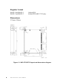
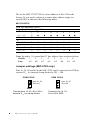
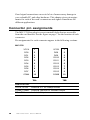
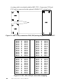
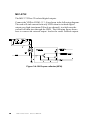
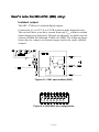
1
MIC 2000
USER'S
MANUAL
MIC-2750/2752
16/32-channel Isolated
Digital Output Card
Modular
Industrial
Computer
PC-Based Modular Industrial Computer
i
Designed for Industrial Automation
Copyright
This documentation is copyrighted 1997 by Advantech Co., Ltd. All
rights are reserved. Advantech Co., Ltd. reserves the right to make
improvements in the products described in this manual at any time
without notice.
No part of this manual may be reproduced, copied, translated or
transmitted in any form or by any means without the prior written
permission of Advantech Co., Ltd. Information provided in this
manual is intended to be accurate and reliable. However, Advantech
Co., Ltd. assumes no responsibility for its use, nor for any infringements of the rights of third parties which may result from its use.
Acknowledgments
PC-LabCard is a trademark of Advantech Co., Ltd.
IBM and PC are trademarks of International Business Machines
Corporation.
Part No. 2003000180 2nd Edition
Printed in Taiwan July 1997
ii
Contents
Chapter 1: General information ....................................................... 1
Introduction ............................................................................ 2
Features .................................................................................. 2
Applications ........................................................................... 2
Software support ................................................................... 2
Specifications ......................................................................... 3
MIC-2750 .......................................................................................3
MIC-2752 .......................................................................................3
Register format ..............................................................................4
Dimensions ....................................................................................4
Chapter 2: Installation .......................................................................5
Initial inspection .................................................................... 6
Switch and jumper settings .................................................. 6
Base address selection (SW1) ........................................................6
Card connector, jumper and switch locations ................................7
Jumper settings (MIC-2752 only) ..................................................8
Chapter 3: Signal connections ......................................................... 9
Connector pin assignments ................................................ 10
Signal connections ............................................................... 13
Isolated output.............................................................................. 13
MIC-2752 ..................................................................................... 14
Chapter 4: Register format .............................................................. 15
Table of Figures
1-1: MIC-2750/2752 layout and dimensions diagram ................................................... 4
2-1: MIC-2750 .............................................................................................................. 7
2-2: MIC-2752 .............................................................................................................. 7
3-1: MIC-2752 (connectors CN2, CN3) wiring diagram to ADAM-3937 ................. 12
3-2: CN1, CN2 and CN3 pin connection mapping ..................................................... 12
3-3: 2803 open collector (NPN) .................................................................................. 13
3-4: ULN 2803 pin configuration ................................................................................ 14
iii
CHAPTER
General information
Chapter 1
1
General information
1
Introduction
The MIC-2750 offers 16 isolated digital output channels, and the
MIC-2752 offers 32 isolated digital output channels. Their isolated
output channels provide 2,500 V of protection.
Each output channel corresponds to a bit in a PC I/O port. This makes
the MIC-2750 and MIC-2752 very easy to program.
Features
• 16/32 isolated DO channels
• High output driving capacity
• High-voltage isolation on isolated output channels (2,500 VDC)
• Connectors:
MIC-2750: Phoenix terminal (removable)
MIC-2752: Shrouded header connector
• High sink current on isolated output channels (200 mA/channel)
• LED (red) output logic status indicator (MIC-2750 only)
Applications
• Industrial ON/OFF control
• BCD interfacing
• Digital I/O control
• Industrial and lab automation
Software support
Free drivers can be downloaded from Advantech's home page at
http://www.advantech.com.tw/techhome/tech1.htm
2
MIC-2750/2752 User's Manual
Specifications
MIC-2750
Digital outputs
•
•
•
•
•
•
Number of outputs: 16
Number of commons: 2 (internally connected)
Output voltage: 5 to 40 VDC, open collector (NPN)
Sink current: 200 mA max. per channel
Isolation voltage: 2500 VDC
Throughput: 10 kHz
Front LEDs
• Number of indicator LEDs: 16
• Indication mode:
Logic "1": LED On
Logic "0": LED Off
Front headers
• Type: Phoenix plug-in screw terminal block (with 20 positions)
• Pin spacing: 5.0 mm
• Wire sizes: Accepts 0.5 mm to 2.5 mm. 1-#12 or 2-#14 to #22
AWG
Power consumption: 1.5 W @ 5 V
MIC-2752
Digital output
•
•
•
•
•
•
Number of output: 32
Number of commons: 32 (internally connected)
Output voltage: 5 to 40 VDC open collector (NPN)
Sink current: 200 mA max. per channel
Isolated voltage: 2500 VDC
Throughput: 10 kHz
Front Headers
• Type: Shrouded header connector
Power consumption: 1 W @ 5 V
Chapter 1
General information
3
Register format
BASE+0 and BASE+1
BASE+2 and BASE+3
Isolated DO
Isolated DO (MIC-2752 only)
Dimensions
122 mm x 185 mm
Figure 1-1: MIC-2750/2752 layout and dimensions diagram
4
MIC-2750/2752 User's Manual
CHAPTER
Installation
Chapter 2
2
Installation
5
Initial inspection
We carefully inspected the MIC-2750/2752 both mechanically and
electrically before shipment. It should be free of marks and in perfect
order upon receipt.
As you unpack the MIC-2750/2752, check it for signs of shipping
damage (damaged box, scratches, dents, etc.). If it is damaged or fails
to meet specifications, notify our service department or your local
sales representative immediately. Also, call the carrier immediately
and retain the shipping carton and packing material for inspection by
the carrier. We will then make arrangements to repair or replace the
unit.
Discharge any static electricity on your body before you touch the
board by touching the back of the system unit (grounded metal).
Remove the MIC-2750/2752 card from its protective packaging by
grasping the rear metal panel. Handle the card only by its edges to
avoid static electric discharge which could damage its integrated
circuits. Keep the antistatic package. Whenever you remove the card
from the PC, please store the card in this package for protection.
You should also avoid contact with materials that hold static electricity such as plastic, vinyl and Styrofoam.
Switch and jumper settings
The MIC-2750/2752 card has one function switch and four jumper
settings. The following sections explain how to configure the card.
You may want to refer to the opposite page for help identifying card
components.
Base address selection (SW1)
You control the MIC-2750/2752's operation by reading or writing
data to the PC's output port addresses. The MIC-2750/2752 requires
four consecutive address locations. Switch SW1 sets the card's base
(beginning) address. Valid base addresses range from Hex 000 to Hex
3FC. Other devices in your system may, however, be using some of
these addresses.
6
MIC-2750/2752 User's Manual
Card connector, jumper and switch locations
TBA
TBB
DO1
VCCA
DO2
DO0
DO3
DO4
DO5
DO6
DO7
COMA
VCCB
DO8
DO9
DO10
DO11
DO12
DO13
DO14
DO15
COMB
+ + + + + + + +
D15 D14 D13 D12 D11 D10 D9 D8
D7 D6 D5 D4 D3 D2 D1 D0
MIC-2750 REV. A2 01-1
16 CHANNEL ISOLATED OUTPUT
A(9 8 7 6 5 4 3 2)
SW1
DIPSW
Figure 2-1: MIC-2750
D0_31
D0_0
1
CN1
CN2
+
D1
63
MIC-2752 32 CH ISOLATION DIGITAL OUTPUT REV.A2
COM4
JP4
PIN16
COM3
JP3
PIN32
COM2
JP2
PIN48
COM1
JP1
PIN64
GND
GND
GND
GND
A( 9 8 7 6 5 4 3 2)
SW1
DIPSW
Figure 2-2: MIC-2752
Label
TBA
TBB
Function
Isolated output terminal block
MIC-2750
Isolated output terminal block
MIC-2750
SW1
CN1
Card base address
MIC-2750/2752
Isolated output connector
MIC-2752
JP1~JP4
Set pins 16, 32, 48, 64 to GRD/external VCC
MIC-2752
Chapter 2
Installation
7
We set the MIC-2750/2752 for a base address of Hex 300 at the
factory. If you need to adjust it to some other address range, set
switch SW1 as shown in the following tables:
MIC-2750/2752
Card I/O addresses (SW1)
Range (hex)
Switch position
1
2
3
4
5
6
7
8
200 - 203
204 - 207
x
*300 - 303
x
3F0 - 3F3
3F4 - 3F7
¡
¡
l
l
l
l
l
l
l
l
l
l
l
l
l
¡
¡
¡
l
l
l
l
l
l
¡
¡
¡
¡
¡
¡
¡
¡
¡
¡
¡
¡
l
l
l
¡
¡= Off
l = On
* = default
Note: Switches 1-8 control the PC bus address lines as shown below:
Switch
1
2
3
4
5
6
7
8
Line
A9 A8
A7
A6
A5
A4
A3 A2
Jumper settings (MIC-2752 only)
Pins 16, 32, 48 and 64 in the MIC-2752 can be connected to GND or
external VCC for integral clamp diodes by JP1 ~ JP4.
COM 1/2/3/4
COM 1/2/3/4
pins 16, 32,
48 or 64
GND
Connect pins 16, 32, 48 or 64 to
external VCC for clamp diodes
8
MIC-2750/2752 User's Manual
pins 16, 32,
48 or 64
GND
Connect pins 16, 32,
48 or 64 to GND
CHAPTER
Signal connections
Chapter 3
3
Signal connections
9
Good signal connections can avoid a lot of unnecessary damage to
your valuable PC and other hardware. This chapter gives pin assignments for each of the card's connectors and signal connections for
different applications.
Connector pin assignments
The MIC-2750 has plug-in screw terminal blocks that are accessible
from the card bracket. See the figure on page 7 for the location of each
connector.
Pin assignments for each connector appear in the following sections.
MIC-2750
VCCA
1
VCCB
1
DO0
2
DO8
2
DO1
3
DO9
3
DO2
4
DO10
4
DO3
5
DO11
5
DO4
6
DO12
6
DO5
7
DO13
7
DO6
8
DO14
8
DO7
9
DO15
9
COMA
10
COMB
10
TBA
TBB
Abbreviations
10
VCCA, VCCB
External VCC for clamp diodes
COMA, COMB
External ground for isolated output
D0 ~ D15
Isolated output
MIC-2750/2752 User's Manual
The MIC-2752 has a 64-pin ribbon cable connector that is accessible
from the card bracket. See the figure on page 7 for the location of each
connector.
MIC-2752
GND/COM1
64
63
DO0
GND
62
61
DO1
GND
60
59
DO2
...
.
.
...
GND
.
.
GND/COM2
48
.
GND
.
.
...
.
.
GND
.
.
GND/COM3
32
.
GND
.
.
...
.
.
GND
.
.
GND/COM4
16
.
GND
.
...
.
5
DO29
...
4
3
DO30
GND
2
1
DO31
CN1
Abbreviations
COM 1/2/3/4
External VCC for clamp diodes
GND
External ground for isolated output
D00 ~ DO31
Isolated output
Pins 16, 32, 48 and 64 can be set to GND or COM 1/2/3/4 by JP1 ~ JP4.
Chapter 3
Signal connections
11
A wiring cable is included with the MIC-2752. Connectors CN2 and
CN3 can be connected to the optional ADAM-3937 wiring board.
Figure 3-1: MIC-2752 (connectors CN2, CN3) wiring diagram to ADAM-3937
CN 1-64
CN 1-62
CN 1-60
CN 1-58
CN 1-56
CN 1-54
CN 1-52
CN 1-50
CN 1-48
CN 1-46
CN 1-44
CN 1-42
CN 1-40
CN 1-38
CN 1-36
CN 1-34
Û
Û
Û
Û
Û
Û
Û
Û
Û
Û
Û
Û
Û
Û
Û
Û
CN 2-35
CN 2-34
CN 2-33
CN 2-32
CN 2-31
CN 2-30
CN 2-29
CN 2-28
CN 2-27
CN 2-26
CN 2-25
CN 2-24
CN 2-23
CN 2-22
CN 2-21
CN 2-20
CN 1-63
CN 1-61
CN 1-59
CN 1-57
CN 1-55
CN 1-53
CN 1-51
CN 1-49
CN 1-47
CN 1-45
CN 1-43
CN 1-41
CN 1-39
CN 1-37
CN 1-35
CN 1-33
Û
Û
Û
Û
Û
Û
Û
Û
Û
Û
Û
Û
Û
Û
Û
Û
CN 2-16
CN 2-15
CN 2-14
CN 2-13
CN 2-12
CN 2-11
CN 2-10
CN 2-9
CN 2-8
CN 2-7
CN 2-6
CN 2-5
CN 2-4
CN 2-3
CN 2-2
CN 2-1
CN 1-32
CN 1-30
CN 1-28
CN 1-26
CN 1-24
CN 1-22
CN 1-20
CN 1-18
CN 1-16
CN 1-14
CN 1-12
CN 1-10
CN 1-8
CN 1-6
CN 1-4
CN 1-2
Û
Û
Û
Û
Û
Û
Û
Û
Û
Û
Û
Û
Û
Û
Û
Û
CN 3-35
CN 3-34
CN 3-33
CN 3-32
CN 3-31
CN 3-30
CN 3-29
CN 3-28
CN 3-27
CN 3-26
CN 3-25
CN 3-24
CN 3-23
CN 3-22
CN 3-21
CN 3-20
CN 1-31
CN 1-29
CN 1-27
CN 1-25
CN 1-23
CN 1-21
CN 1-19
CN 1-17
CN 1-15
CN 1-13
CN 1-11
CN 1-9
CN 1-7
CN 1-5
CN 1-3
CN 1-1
Û
Û
Û
Û
Û
Û
Û
Û
Û
Û
Û
Û
Û
Û
Û
Û
CN 3-16
CN 3-15
CN 3-14
CN 3-13
CN 3-12
CN 3-11
CN 3-10
CN 3-9
CN 3-8
CN 3-7
CN 3-6
CN 3-5
CN 3-4
CN 3-3
CN 3-2
CN 3-1
Figure 3-2: CN1, CN2, CN3 pin connection mapping
12
MIC-2750/2752 User's Manual
Signal connections
Isolated output
The MIC-2750 has 16 isolated digital outputs.
Connect the VDD to VCCA or VCCB as shown in the diagram below.
The card will sink your drive current from only VDD when its isolated
digital output goes high (max. 200 mA per channel), in which case the
current will then flow through COMA or COMB. The following figure
shows how to connect an external output load to the card's isolated
outputs:
Figure 3-3: 2803 open collector(NPN)
11
10
9
12
7
8
13
15
4
6
16
3
14
17
2
5
18
1
ULN 2803
Figure 3-4: ULN 2803 pin configuration
Chapter 3
Signal connections
13
MIC-2752
The MIC-2752 has 32 isolated digital outputs.
Connect the VDD to COM1 (2, 3, 4) as shown in the following diagram.
The card will sink current from only VDD when its isolated digital
output goes high (maximum 200 mA per channel), in which case the
current will then pass through the GND. The following figure shows
how to connect an external output load to the card's isolated outputs.
Figure 3-4: 2803 open collector (NPN)
14
MIC-2750/2752 User's Manual
CHAPTER
Register format
Chapter 4
4
Register format
15
Programming the MIC-2750/2752 is extremely simple. Each I/O channel
corresponds to a bit in the card's registers. To turn on an output
channel you write a ‘‘1” to the corresponding bit.
The MIC-2750 requires eight I/O register addresses, but you only need
to access the first two registers (data registers). The MIC-2752
requires four I/O register addresses, each of which needs to be
accessed. The address of each register is specified as an offset from
the card's base address. For example, BASE+0 is the card's base
address and BASE+2 is the base address + two bytes. If the card's
base address is 300h, the register's address is 302h. See Chapter 2 for
information on setting the card's base address.
Register assignments are as follows:
16
BASE+0
Write
DO bits 0-7
Read
N/A
MIC-2750/2752
BASE+1
DO bits 8-15
N/A
MIC-2750/2752
BASE+2
DO bits 16-23 N/A
MIC-2752
BASE+3
DO bits 24-31 N/A
MIC-2752
MIC-2750/2752 User's Manual
User's note for MIC-2750 (PNP) only:
Isolated output
The MIC-2750 has 16 isolated digital outputs.
Connect the VDD to VCCA or VCCB as shown in the diagram below.
The card will drive your drive current from only VDD when its isolated
digital output goes high (max. 200 mA per channel), in which case the
current will then flow through COMA or COMB. The following figure
shows how to connect an external output load to the card's isolated
outputs:
16
15
14
13
12
11
3
4
5
6
7
8
Gnd
17
2
vs
18
1
Figure 4-1: 2981 open emitter (PNP)
Figure 4-2: UDN 2981 pin configuration
Chapter 4
Register format
17
18
MIC-2750/2752 User's Manual