1
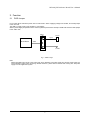
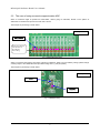
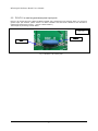
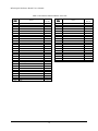
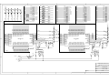
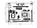
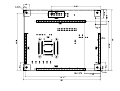
FEBL610Q174-01 ML610Q174 Reference Board User’s Manual Issue Date: Dec 5, 2013 ML610Q174 Reference Board User’s Manual NOTES No copying or reproduction of this document, in part or in whole, is permitted without the consent of LAPIS Semiconductor Co., Ltd. The content specified herein is subject to change for improvement without notice. The content specified herein is for the purpose of introducing LAPIS Semiconductor 's products (hereinafter "Products"). If you wish to use any such Product, please be sure to refer to the specifications, which can be obtained from LAPIS Semiconductor upon request. Examples of application circuits, circuit constants and any other information contained herein illustrate the standard usage and operations of the Products. The peripheral conditions must be taken into account when designing circuits for mass production. Great care was taken in ensuring the accuracy of the information specified in this document. However, should you incur any damage arising from any inaccuracy or misprint of such information, LAPIS Semiconductor shall bear no responsibility for such damage. The technical information specified herein is intended only to show the typical functions of and examples of application circuits for the Products. LAPIS Semiconductor does not grant you, explicitly or implicitly, any license to use or exercise intellectual property or other rights held by LAPIS Semiconductor and other parties. LAPIS Semiconductor shall bear no responsibility whatsoever for any dispute arising from the use of such technical information. The Products specified in this document are intended to be used with general-use electronic equipment or devices (such as audio visual equipment, office-automation equipment, communication devices, electronic appliances and amusement devices). The Products specified in this document are not designed to be radiation tolerant. While LAPIS Semiconductor always makes efforts to enhance the quality and reliability of its Products, a Product may fail or malfunction for a variety of reasons. Please be sure to implement in your equipment using the Products safety measures to guard against the possibility of physical injury, fire or any other damage caused in the event of the failure of any Product, such as derating, redundancy, fire control and fail-safe designs. LAPIS Semiconductor shall bear no responsibility whatsoever for your use of any Product outside of the prescribed scope or not in accordance with the instruction manual. The Products are not designed or manufactured to be used with any equipment, device or system which requires an extremely high level of reliability the failure or malfunction of which may result in a direct threat to human life or create a risk of human injury (such as a medical instrument, transportation equipment, aerospace machinery, nuclear-reactor controller, fuel-controller or other safety device). LAPIS Semiconductor shall bear no responsibility in any way for use of any of the Products for the above special purposes. If a Product is intended to be used for any such special purpose, please contact a ROHM sales representative before purchasing. If you intend to export or ship overseas any Product or technology specified herein that may be controlled under the Foreign Exchange and the Foreign Trade Law, you will be required to obtain a license or permit under the Law. Copyright 2013 LAPIS Semiconductor Co., Ltd. 1 ML610Q102 Reference Board User’s Manual Preface This manual describes the operation of the ReferenceBoard of the 8-bit microcontroller ML610Q174. The following manuals are also available. Read them as necessary. ML610Q174 User’s Manual Description on the operation of the hardware of the 8-bit microcontroller ML610Q174. ML610Q172 / ML610Q173 User’s Manual Description on the operation of the hardware of the 8-bit microcontroller ML610Q172/ML610Q173. uEASE User’s Manual Description on the on-chip debug tool uEASE. 2 ML610Q174 Reference Board User’s Manual 1. Overview 1.1 Features ML610Q174 Reference board is prepared by LAPIS SEMICONDUCTOR to have you study the operations of ML610Q174. The board is arranged so that necessary components are mounted by you according to your purpose, then only minimum necessary components are mounted on the board by LAPIS SEMICONDUCTOR for brief use of ML610Q174. By using the board with "uEASE on-chip debug emulator" (hereinafter referred to "uEASE") and "free sample U8 Development Tools CD-ROM" which is bundled in the package of uEASE not only Software development/debugging but also writing Flash ROM in the devices are capable. This board also works in stand alone mode with external power suppy without uEASE. ML610Q172 and ML610Q173 exist as 64 pin versions of ML610Q174. Please use this board also for development and debugging of the software of ML610Q172. Please refer to “ML610Q172/ML610Q173 User’s Manual” for the detail of ML610Q174 and ML610Q172/ML610Q173. Before starting works with this board, read below carefully and understand notices. The hardware specification of this board is shown below. Embedded microcontroller U1/U2(Mounting / IC-Socket): ML610Q174 ・ UVDD、VSS: Input power supply pin ・ PWR: Jumper for input power supply switch ( 3pin pin-header and short pin ) ・ CNUE: Connector for on-chip debug emulator ( 14pin connector ) ・ XT_1/XT_2(Mounting / IC-Socket ): 32.768kHz oscillator ・ OSC_1/OSC_2(Mounting / IC-Socket): 8MHz oscillator ・ P20-P23,P90-P91: Light emitting diodes Embedded parts ・ C1-C3/C10-C12(Mounting / IC-Socket): Capacitors for LCD external input voltage connection(3 pieces) ・ C4/C13(Mounting / IC-Socket): Capacitors for RESET_N pin. ・ C5/C14(Mounting / IC-Socket): Capacitors for VREF input voltage connection. ・ C6-C7/C15-C16: Capacitors for input voltage ( 2pieces ) ・ C8-C9/C17-C18(Mounting / IC-Socket): Capacitors for 32.768kHz oscillator ( 2pieces ) ・ R1-R6: Resistance for light emitting diodes (P20-P23,P90-P91) ・ R7-R9/R10-R12(Mounting / IC-Socket): Resistance for LCD external input voltage connection(3 pieces) ・ SP1-SP6: Lands for light emitting diodes. ・ SP9-SP10(Mounting / IC-Socket): Lands for P10, P11 terminal connection Pads for mounting ・ SP16/SP19(Mounting / IC-Socket): Pads for bonding of P85/VL2 and LCD external input voltage. ・ SP17/SP20(Mounting / IC-Socket): Pads for bonding of P84/VL1 and LCD external input voltage. ・ AIN0-AIN11: Land for SA-ADC terminal connection ・ CN1-CN4: Pads for peripheral board connectors( 30pin×2、20pin×2、2.54mm pitch) Other useful pads ・ VDD、VSS、UVDD、VREF、AIN0-AIN11 Operating voltage ・ VDD = +2.2V to +5.5V、VREF = +4.5V to +5.5V Board size ・ 100.00 x 120.00 mm This board is made on the assumption that it is used carrying in a user circuit. When used with this board simple substance, please use on an insulating material. An operation abnormality may be caused when used on a conductive material. ML610Q174 of the engineering sample may be carried in this board. Please confirm the final confirmation of an electrical property etc. on mass production goods and customer's production board. The support about this board is not accepted. Only in the case of initial failure, exchange responds. 3 ML610Q102 Reference Board User’s Manual 1.2 The external view of a board The external view of ML610Q174 ReferenceBoard is shown. CN1 PWR CNUE UVDD VSS XT_2 XT_1 OSC_2 OSC_1 CN4 VREF U2 Socket U1 Mounting CN2 P90-P91 P20-P23 CN3 Fig.1. ML610Q174 ReferenceBoard External view 1pin Fig.2. Direction of device set When a device is set to a reference board, please carry out, where the power is turned off. Moreover, please set not to mistake the direction of a device. 4 ML610Q174 Reference Board User’s Manual 2. Function 2.1 PWR Jumper It is a jumper which selects the power source of this board. When supplying voltage from uEASE, set a PWR jumper to the "uE" side. The ability to supply power of the uEASE is +3.3v/100mA. When a power supply is inputted from the external, please input between check pin UVDD-VSS and set a PWR jumper to the "USR" side. PWR uE CNUE 13pin ML610Q174 VDD UVDD USR Fig.3. PWR Jumper Note: Where the PWR jumper is set to the "USR" side, when uEASE is connected, please turn ON the power supply of a user application system after connecting uEASE. Moreover, please remove uEASE after turning OFF the power supply of a user application system. 5 ML610Q102 Reference Board User’s Manual 2.2 The case of using successive approximation ADC When a conversion target is inputted into AIN0-AIN11, without going via CN1/CN4, Please cut the pattern of AIN0-AIN11 if needed and input from the hole near a device. The example of processing is shown below. Top View Cut Pattern Please input directly from the hole of the side here after cutting. Fig.4. AIN0-AIN15 (SA-ADC) VREF is connected with VDD by the jumper at the time of shipment. When you input arbitrary voltage, please change a VREF jumper to the USER side and input VREF voltage from 1_CN6 pin (VREF). The example of processing is shown below. Top View Short Remove Fig.5. VREF(SA-ADC) 6 ML610Q174 Reference Board User’s Manual 2.3 The case of using light emitting diodes P20-P23, P90-P91 can drive direct to light emitting diodes. P20-P23, P90-P91 are wired with light emitting diodes on this board. Please remove the parts mounted in SP1-SP6. The example of processing is shown below. Top View Remove Fig.6. SP1-SP5 pads 2.4 The case of driving LCDs The chip resistor of 2012 sizes can be mounted between VL3 to VDD (SP7/SP11 pad). At the time of shipment, since VDD and VL3 short-circuit, please mount a chip resistor in SP7/SP11 if needed. Please refer to figure 6.( VL3 ) The example of processing is shown below. Top View Fig.7. SP7/SP11 pads Note: It is a short condition between VL3 and LCD driving voltage input pin (SP15/SP18). Moreover, it is an open condition between P85/VL2 and an LCD driving voltage input pin (SP16/SP19 pad) and between P85/VL2 and LCD driving voltage input pin (SP17/SP20). As for the method of using VL3, P85/VL2 and P84/VL1 as LCD driving power sources, the following three kinds of methods exist. ・ The LCD external input voltage on a reference board is used. ・ Voltage is inputted from CN1_24 to 26. ・ Voltage is generated using a built-in LCD resistance. Please be careful for the LCD external input voltage on a reference board, the voltage inputted from CN1_24~26, and the voltage generated inside LSI not to short-circuit. 7 ML610Q102 Reference Board User’s Manual 2.5 P10-P11 is used as general purpose input ports P10-P11 can change and use a 8MHz oscillation terminal and a general input port terminal. When you use it as a general input port terminal, please remove an 8MHz oscillator and short-circuit SP9/SP10 and SP13/SP14, respectively. Please refer to figure 7. ( P10,P11 8MHz oscillator ) The example of processing is shown below. Top View Remove Short Fig.7. SP9/SP10、SP13/SP14 pads 8 ML610Q174 Reference Board User’s Manual 3. User interface 3.1 The user interface of ML610Q174 Reference Board The pin assignment of CN1, CN2, CN3 and CN4 of the reference board embedded ML610Q174 in below is shown. Table 1. ML610Q174 Reference Board CN1 / CN2 CN1 Name 1 2 P44/T0P4CK/AIN4/SIN0 P33/AIN3 3 4 5 6 7 8 9 10 11 12 13 14 15 16 17 18 19 20 21 22 23 24 25 26 27 28 29 30 P32/AIN2 P31/PW6EV1/AIN1 P30/PW45EV1/AIN0 VREF P50/AIN8/SIN1 P51/AIN9/SCK1 P52/CMP0P/RXD1/SOUT1 P53/CMP1P/TXD1/PWM6/TXD0 P34/AIN11/PWM4 P35/AIN10/PWM5 P36/LSCLK NC NC P10/OSC0 P11/OSC1 VSS UVDD NC NC NC NC VL3 P85/VL2 P84/VL1 P83/COM3 P82/COM2 P81/COM1 P80/COM0 LSI Pin No. 19 20 21 22 23 24 15 14 13 12 10 11 33 ----25 26 27 28 --------34 35 36 37 38 39 40 9 CN2 Name 1 2 SEG0 SEG1 LSI Pin No. 41 42 3 4 5 6 7 8 9 10 11 12 13 14 15 16 17 18 19 20 SEG2 SEG3 SEG4 SEG5 SEG6 SEG7 PC0/SEG8 PC1/SEG9 PC2/SEG10 PC3/SEG11 PC4/SEG12 PC5/SEG13 PC6/SEG14 PC7/SEG15 PD0/SEG16 PD1/SEG17 PD2/SEG18 PD3/SEG19 43 44 45 46 47 48 49 50 51 52 53 54 55 56 57 58 59 60 ML610Q102 Reference Board User’s Manual Table 2. ML610Q174 Reference Board CN3 / CN4 CN3 Name 1 2 3 4 5 6 7 8 9 10 11 12 13 14 15 16 17 18 19 20 21 22 23 24 25 26 27 28 29 30 PD4/SEG20 PD5/SEG21 PD6/SEG22 PD7/SEG23 NC NC NC NC NC NC NC NC PF0/SEG32/SIN0 PF1/SEG33/SCK0 PF2/SEG34/RXD0/SOUT0 PF3/SEG35/TXD0/PWM4/TXD1 PF4/SEG36/SIN1/PWM4 PF5/SEG37/SCK1/PWM5 PF6/SEG38/RXD1/SOUT1/PWM6 PF7/SEG39/TXD1/TXD0 RESET_N P40/SDA/SIN0 P41/SCL/SCK0 P42/RXD0/SOUT0 P43/TXD0/PWM4/TXD1 P00/EXI0/PW45EV0 P01/EXI1/PW6EV0 P02/EXI2/RXD0 P03/EXI3/RXD1 NC LSI Pin No. 61 62 63 64 ----------------65 66 67 68 69 70 71 72 32 6 7 8 9 75 76 77 78 --- 10 CN4 Name LSI Pin No. 1 2 3 4 5 6 7 8 9 10 11 12 13 14 15 16 17 18 19 20 P20/LED0/LSCLK/PWM4 P21/LED1/OUTCLK/PWM5 P22/LED2/TM9OUT P23/LED3/TMBOUT VSS P90/LED4 P91/LCD5 NC NC NC NC NC NC NC NC NC NC P47/T9BCK/AIN7/CMP1M P46/T8AP6CK/AIN6/CMP0M P45/T1P5CK/AIN5 79 80 2 3 1 4 5 --------------------16 17 18 ML610Q174 Reference Board User’s Manual 4. The circuit diagram and substrate dimensional drawing The circuit diagram and substrate dimensional drawing of this board are shown after a next page. 11 A B P20 560 R6 P21 LED 560 R5 P22 LED 560 R4 P23 LED 560 R3 P90 LED 560 R2 P91 LED 1 LED 560 R1 VDD PIN2 2/1D PIN3 2/1D PIN4 2/1D PIN5 2/1D PIN6 PIN7 2/2C 2/2C PIN8 2/2C PIN9 2/2C SP6 PIN79 SP5 PIN80 SP4 PIN2 SP3 SP2 PIN3 PIN4 PIN5 SP1 PIN10 PIN11 AIN11 2/1A PIN13 2/1A PIN14 AIN9 P23/LED3 I/O P90/LED4 I/O P91/LED5 I/O P40/SDA I/O P41/SCL PIN15 PIN16 P43/TXD0 I/O P34/AIN11 P35/AIN10 I/O P53/TXD1 P52/RXD1 I/O 2/1A I/O 2/1A AIN3 2/1A AIN2 PIN21 2/1A AIN1 PIN22 P51/AIN9 2/2D AIN4 PIN20 I/O 2/2D AIN5 PIN18 I/O 2/2D AIN6 PIN17 P42/RXD0 2/1A AIN7 PIN19 2/2A PIN12 P22/LED2 I/O I/O 2/1A AIN10 I/O 2/1A AIN0 PIN23 D C AIN8 2/1A I/O I/O I/O I/O I/O I/O I/O I/O I/O P50/AIN8 P47/AIN7 P46/AIN6 P45/AIN5 P44/AIN4 P33/AIN3 P32/AIN2 P31/AIN1 P30/AIN0 PIN32 PIN33 2/2C 2/2A PIN34 2/2A PIN35 2/2A PIN36 PIN37 2/2A 2/2A PIN38 2/2A PIN39 2/2A PIN40 PIN41 2/2A 2/1B PIN42 2/1B PIN43 2/1B PIN44 2/1B PIN45 2/1B PIN46 2/1B PIN47 2/1B PIN48 2/1B I/O RESET_N I/O I/O P36/LSCLK VL3 I/O P85/VL2 I/O P84/VL1 I/O P83/COM3 I/O P82/COM2 P81/COM1 I/O P80/COM0 I/O SEG0 SEG1 I/O SEG2 I/O SEG3 I/O SEG4 SEG5 I/O I/O SEG6 I/O SEG7 PIN51 PIN52 I/O I/O PIN49 PIN50 2/1B 2/1B 2/1B 2/2B PIN53 PIN54 2/2B PIN55 2/2B PIN56 2/2B PIN57 PIN58 2/2B PIN59 2/2B 2/2B PIN60 2/2B 2/2B PIN61 PIN62 2/1C PIN63 2/1C PIN64 2/1C 2/1C I/O PC0/SEG8 I/O I/O PC1/SEG9 PC2/SEG10 I/O PC3/SEG11 I/O PC4/SEG12 I/O PC5/SEG13 I/O PC6/SEG14 I/O PC7/SEG15 I/O PD0/SEG16 I/O PD1/SEG17 PD2/SEG18 I/O I/O PD3/SEG19 I/O PD4/SEG20 I/O PD5/SEG21 PD6/SEG22 I/O I/O PD7/SEG23 PIN65 PIN66 2/2C 2/2C PIN67 2/2C PIN68 2/2C PIN69 PIN70 2/2C 2/2C PIN71 2/2C PIN72 2/2C PIN73 PIN74 2/3A 2/3A PIN75 2/2C PIN76 2/2C PIN77 PIN78 2/2C 2/2C PIN79 2/1D PIN80 2/1D PF0/SEG32 I/O I/O PF1/SEG33 PF2/SEG34 I/O PF3/SEG35 I/O PF4/SEG36 I/O PF5/SEG37 I/O PF6/SEG38 I/O PF7/SEG39 I/O TEST0 I/O I/O TEST1_N P00/EXI0 I/O P01/EXI1 I/O P02/EXI2 I/O P03/EXI3 I/O P20/LED0 I/O P21/LED1 VDD SP7 VSS PIN64 PIN63 PIN62 PIN61 PIN60 PIN59 PIN58 PIN57 PIN56 PIN55 PIN54 PIN53 PIN52 PIN51 PIN50 PIN49 PIN48 PIN47 PIN46 PIN45 PIN44 PIN43 PIN42 PIN41 VSS IN 200K R10 0.22UF C12 PIN36 C13 VSS PIN32 SP20 200K R12 2.2UF 2 VSS 12PF 1 3 VSS VSS OSC_2 1 VSS SP14 VSS 3 2 SP13 SP9 VDD SP19 XT_2 2 VDD USR 3 SP10 PIN24 VREF_IN 0.22UF C11 PIN35 SP22 PIN2 PIN3 PIN4 PIN5 PIN6 PIN7 PIN8 PIN9 PIN10 PIN11 PIN12 PIN13 PIN14 PIN15 PIN16 PIN17 PIN18 PIN19 PIN20 PIN21 PIN22 PIN23 PIN24 OSC_1 1 C 2/1A PIN40 PIN39 PIN38 PIN37 PIN36 PIN35 PIN34 PIN33 PIN32 1UF C14 PIN2 PIN3 PIN4 PIN5 PIN6 PIN7 PIN8 PIN9 PIN10 PIN11 PIN12 PIN13 PIN14 PIN15 PIN16 PIN17 PIN18 PIN19 PIN20 PIN21 PIN22 PIN23 PIN24 1UF C5 PIN[80:1] 40 39 38 37 36 35 34 33 32 31 30 29 28 27 26 25 200K R11 64 63 62 61 60 59 58 57 56 55 54 53 52 51 50 49 48 47 46 45 44 43 42 41 U2 2 C18 VSS C9 12PF C8 12PF VSS 2 IC_SOCKET P80/COM0 P81/COM1 P82/COM2 P83/COM3 P84/VL1 P85/VL2 VL3 P36/LSCLK RESET_N XT1 XT0 VDDL VDD VSS_27 P11/OSC1 P10/OSC0 C17 12PF XT_1 1 PF0/SEG32 PF1/SEG33 PF2/SEG34 PF3/SEG35 PF4/SEG36 PF5/SEG37 PF6/SEG38 PF7/SEG39 TEST0 TEST1_N P00/EXI0 P01/EXI1 P02/EXI2 P03/EXI3 P20/LED0 P21/LED1 C16 10UF SP12 PIN32 SP17 65 66 67 68 69 70 71 72 73 74 75 76 77 78 79 80 C15 10UF C4 200K R9 2.2UF C3 PIN65 PIN66 PIN67 PIN68 PIN69 PIN70 PIN71 PIN72 PIN73 PIN74 PIN75 PIN76 PIN77 PIN78 PIN79 PIN80 PD7/SEG23 PD6/SEG22 PD5/SEG21 PD4/SEG20 PD3/SEG19 PD2/SEG18 PD1/SEG17 PD0/SEG16 PC7/SEG15 PC6/SEG14 PC5/SEG13 PC4/SEG12 PC3/SEG11 PC2/SEG10 PC1/SEG9 PC0/SEG8 SEG7 SEG6 SEG5 SEG4 SEG3 SEG2 SEG1 SEG0 C2 VSS_1 P22/LED2 P23/LED3 P90/LED4 P91/LED5 P40/SDA P41/SCL P42/RXD0 P43/TXD0 P34/AIN11 P35/AIN10 P53/TXD1 P52/RXD1 P51/AIN9 P50/AIN8 P47/AIN7 P46/AIN6 P45/AIN5 P44/AIN4 P33/AIN3 P32/AIN2 P31/AIN1 P30/AIN0 VREF PIN36 0.22UF SP18 VSS VSS 200K R8 SP16 SP21 VSS 3 0.22UF PIN35 VSS PIN40 PIN39 PIN38 PIN37 PIN36 PIN35 PIN34 PIN33 PIN32 1 2 3 4 5 6 7 8 9 10 11 12 13 14 15 16 17 18 19 20 21 22 23 24 VSS_1 P22/LED2 P23/LED3 P90/LED4 P91/LED5 P40/SDA P41/SCL P42/RXD0 P43/TXD0 P34/AIN11 P35/AIN10 P53/TXD1 P52/RXD1 P51/AIN9 P50/AIN8 P47/AIN7 P46/AIN6 P45/AIN5 P44/AIN4 P33/AIN3 P32/AIN2 P31/AIN1 P30/AIN0 VREF U1 40 39 38 37 36 35 34 33 32 31 30 29 28 27 26 25 C7 10UF SP8 ML610Q174 P80/COM0 P81/COM1 P82/COM2 P83/COM3 P84/VL1 P85/VL2 VL3 P36/LSCLK RESET_N XT1 XT0 VDDL VDD VSS_27 P11/OSC1 P10/OSC0 C6 10UF PF0/SEG32 PF1/SEG33 PF2/SEG34 PF3/SEG35 PF4/SEG36 PF5/SEG37 PF6/SEG38 PF7/SEG39 TEST0 TEST1_N P00/EXI0 P01/EXI1 P02/EXI2 P03/EXI3 P20/LED0 P21/LED1 0.22UF C10 PIN34 VDD 65 66 67 68 69 70 71 72 73 74 75 76 77 78 79 80 PD7/SEG23 PD6/SEG22 PD5/SEG21 PD4/SEG20 PD3/SEG19 PD2/SEG18 PD1/SEG17 PD0/SEG16 PC7/SEG15 PC6/SEG14 PC5/SEG13 PC4/SEG12 PC3/SEG11 PC2/SEG10 PC1/SEG9 PC0/SEG8 SEG7 SEG6 SEG5 SEG4 SEG3 SEG2 SEG1 SEG0 64 63 62 61 60 59 58 57 56 55 54 53 52 51 50 49 48 47 46 45 44 43 42 41 200K R7 SP15 VDD PIN65 PIN66 PIN67 PIN68 PIN69 PIN70 PIN71 PIN72 PIN73 PIN74 PIN75 PIN76 PIN77 PIN78 PIN79 PIN80 C1 PIN34 1 2 3 4 5 6 7 8 9 10 11 12 13 14 15 16 17 18 19 20 21 22 23 24 0.22UF PIN64 PIN63 PIN62 PIN61 PIN60 PIN59 PIN58 PIN57 PIN56 PIN55 PIN54 PIN53 PIN52 PIN51 PIN50 PIN49 PIN48 PIN47 PIN46 PIN45 PIN44 PIN43 PIN42 PIN41 2 1 SP11 VDD I/O VREF P10 IN P11 IN 2/2A 2/2A LAPIS Semiconductor Co., Ltd. TITLE 4 ML610Q174 Reference Board APPLICATION ML610Q174 DWG NO DRAWN By A B C QTS-11583 SHEET 1 of 2 D REV 1.00 4 A B CN1 CN30P 1 P44/AIN4 P33/AIN3 P32/AIN2 P31/AIN1 P30/AIN0 VREF_IN P50/AIN8 P51/AIN9 P52/RXD1 P53/TXD1 P34/AIN11 P35/AIN10 P36/LSCLK P10 P11 2 VL3 P85/VL2 P84/VL1 P83/COM3 P82/COM2 P81/COM1 P80/COM0 I/O I/O I/O I/O I/O OUT I/O I/O I/O I/O I/O I/O I/O I/O I/O I/O I/O I/O I/O I/O I/O I/O 1/2A 1/2A 1/2A 1/2A 1/2A 1/4A 1/2A 1/1A 1/1A 1/1A 1/2A 1/2A 1/2A PIN15 PIN14 PIN13 PIN12 PIN10 PIN11 PIN33 1/4B 1/4B 1/2A 1/2A 1/1C 1/2A 1/2A 1/2A 1/2A PIN34 PIN35 PIN36 PIN37 PIN38 PIN39 PIN40 CN3 CN30P CN2 CN20P 1 2 3 4 5 6 7 8 9 10 11 12 13 14 15 16 17 18 19 20 21 22 23 24 25 26 27 28 29 30 PIN19 PIN20 PIN21 PIN22 PIN23 SEG0 SEG1 SEG2 SEG3 SEG4 SEG5 SEG6 SEG7 PC0/SEG8 PC1/SEG9 PC2/SEG10 PC3/SEG11 PC4/SEG12 PC5/SEG13 PC6/SEG14 PC7/SEG15 PD0/SEG16 PD1/SEG17 PD2/SEG18 PD3/SEG19 I/O I/O I/O I/O I/O I/O I/O I/O I/O I/O I/O I/O I/O I/O I/O I/O I/O I/O I/O I/O 1/2A 1/2A 1/2A 1/2A 1/2A 1/2A 1/2A 1/2A 1/2A 1/2A 1/2A 1/2A 1/2A 1/2A 1/2A 1/2A 1/2A 1/2A 1/2A 1/2A D C PIN41 PIN42 PIN43 PIN44 PIN45 PIN46 PIN47 PIN48 PIN49 PIN50 PIN51 PIN52 PIN53 PIN54 PIN55 PIN56 PIN57 PIN58 PIN59 PIN60 1 2 3 4 5 6 7 8 9 10 11 12 13 14 15 16 17 18 19 20 PD4/SEG20 PD5/SEG21 PD6/SEG22 PD7/SEG23 PF0/SEG32 PF1/SEG33 PF2/SEG34 PF3/SEG35 PF4/SEG36 PF5/SEG37 PF6/SEG38 PF7/SEG39 RESET_N P40/SDA P41/SCL P42/RXD0 P43/TXD0 P00/EXI0 P01/EXI1 P02/EXI2 P03/EXI3 I/O I/O I/O I/O I/O I/O I/O I/O I/O I/O I/O I/O I/O I/O I/O I/O I/O I/O I/O I/O I/O 1/2A 1/2A 1/2A 1/2C 1/2A 1/1D 1/1D 1/1D 1/1D 1/1D 1/2A 1/1D 1/2A 1/1A 1/1A 1/1A 1/1A 1/1D 1/1D 1/1D 1/1D PIN61 PIN62 PIN63 PIN64 PIN65 PIN66 PIN67 PIN68 PIN69 PIN70 PIN71 PIN72 PIN32 PIN6 PIN7 PIN8 PIN9 PIN75 PIN76 PIN77 PIN78 CN4 CN20P 1 2 3 4 5 6 7 8 9 10 11 12 13 14 15 16 17 18 19 20 21 22 23 24 25 26 27 28 29 30 P20/LED0 P21/LED1 P22/LED2 P23/LED3 OUT OUT OUT OUT P90/LED4 P91/LED5 OUT OUT P47/AIN7 P46/AIN6 P45/AIN5 I/O I/O I/O 1/1D 1/2A 1/2A 1/2A PIN79 PIN80 PIN2 PIN3 1/1A 1/1A PIN4 PIN5 1/2A 1/2A 1/2A PIN16 PIN17 PIN18 1 1 2 3 4 5 6 7 8 9 10 11 12 13 14 15 16 17 18 19 20 VSS 2 VSS VDD UE C PWR USR UVDD VDD CNUE CN14P 3 3 1 2 3 4 5 6 7 8 9 10 11 12 13 14 PIN74 1/1D PIN73 1/1D IN I/O TEST1_N TEST0 VSS VSS LAPIS Semiconductor Co., Ltd. TITLE 4 ML610Q174 Reference Board APPLICATION ML610Q174 DWG NO DRAWN By A B C QTS-11583 SHEET 2 of 2 D REV 1.00 4