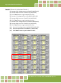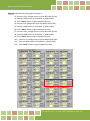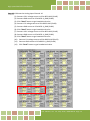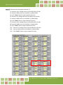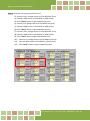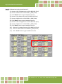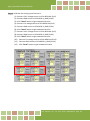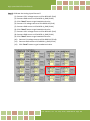
1
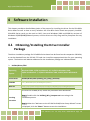
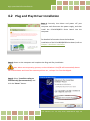
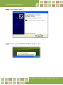
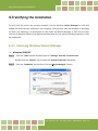
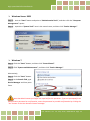
PCIe-862x Series Board User Manual High-speed Multifunction Boards Version 1.0, May 2015 SUPPORT This manual relates to the following boards: PCIe-8620 and PCIe-8622. WARRANTY All products manufactured by ICP DAS are warranted against defective materials for a period of one year from the date of delivery to the original purchaser. WARNING ICP DAS assumes no liability for damages consequent to the use of this product. ICP DAS reserves the right to change this manual at any time without notice. The information furnished by ICP DAS is believed to be accurate and reliable. However, no responsibility is assumed by ICP DAS for its use, nor for any infringements of patents or other rights of third parties resulting from its use. COPYRIGHT Copyright © 2015 by ICP DAS. All rights are reserved. TRADEMARKS Names are used for identification purposes only and may be registered trademarks of their respective companies. CONTACT US If you have any questions, feel to contact us by email at: [email protected] or [email protected] We will respond to you within 2 working days. High-speed Multifunction Boards TABLE OF CONTENTS PACKING LIST ................................................................................................................................................................ 4 1. INTRODUCTION ................................................................................................................................................. 5 1.1 OVERVIEW ............................................................................................................................................................ 5 1.2 FEATURES .............................................................................................................................................................. 6 1.3 SPECIFICATIONS ...................................................................................................................................................... 7 1.4 APPLICATIONS ........................................................................................................................................................ 9 2 HARDWARE CONFIGURATION ...........................................................................................................................10 2.1 BOARD L AYOUT .................................................................................................................................................... 10 2.2 CARD ID SWITCH (SW1) ....................................................................................................................................... 12 2.3 SYSTEM BLOCK DIAGRAM ....................................................................................................................................... 13 2.4 ANALOG INPUT .................................................................................................................................................... 14 2.4.1 Analog Input Block ...................................................................................................................................... 14 2.4.2 Analog Input Range..................................................................................................................................... 15 2.4.3 Connecting Analog Input Signals ................................................................................................................ 16 2.4.4 Signal Shielding ........................................................................................................................................... 16 2.4.5 Analog Input Data Acquisition Methods ..................................................................................................... 17 2.5 ANALOG OUTPUT ................................................................................................................................................. 18 2.5.1 Analog Output Block ................................................................................................................................... 18 2.5.2 Connection Analog Output Signals .............................................................................................................. 19 2.6 DIGITAL INPUT/OUTPUT......................................................................................................................................... 20 2.7 COUNTERS........................................................................................................................................................... 21 2.8 PIN ASSIGNMENTS ................................................................................................................................................ 22 2.8.1 CON1 Connector of the PCIe-8620/8622 ..................................................................................................... 22 2.8.2 I/O Connector Signal Descriptions ............................................................................................................... 23 2.8.3 Power Source............................................................................................................................................... 23 3 HARDWARE INSTALLATION ...............................................................................................................................24 4 SOFTWARE INSTALLATION ................................................................................................................................28 4.1 OBTAINING/INSTALLING THE DRIVER INSTALLER PACKAGE ......................................................................................... 28 4.2 PLUG AND PLAY DRIVER INSTALLATION ...................................................................................................................... 30 4.3 VERIFYING THE INSTALLATION .................................................................................................................................. 32 4.3.1 Accessing Windows Device Manager .......................................................................................................... 32 4.3.2 Check the Installation .................................................................................................................................. 35 User Manual, Ver. 1.0, May 2015, PMH-029-10 Page 2 High-speed Multifunction Boards 5 6 TESTING THE PCIE-8620/8622 SERIES BOARD ......................................................................................................36 5.1 PCIE-8620 SELF-TEST........................................................................................................................................... 36 5.2 PCIE-8622 SELF-TEST........................................................................................................................................... 41 I/O REGISTER ADDRESSES ...................................................................................................................................46 6.1 HARDWARE ID ..................................................................................................................................................... 46 6.2 I/O ADDRESS MAPPING ......................................................................................................................................... 47 6.3 BAR 0 (MMIO) ................................................................................................................................................... 48 6.3.1 Interrupt and Initialize Control/Status Registers ......................................................................................... 48 6.3.2 Digital I/O Registers .................................................................................................................................... 50 6.3.3 Analog Input Registers ................................................................................................................................ 51 6.3.4 Analog Output Registers ............................................................................................................................. 53 6.3.5 Counter Registers ........................................................................................................................................ 54 6.4 BAR 1 (MMIO) ................................................................................................................................................... 55 6.4.1 7 8 Xilinx Spartan-6 Control/Status Registers ................................................................................................... 55 CALIBRATION ....................................................................................................................................................56 7.1 INTRODUCTION..................................................................................................................................................... 56 7.2 STEP-BY-STEP CALIBRATION PROCESS........................................................................................................................ 58 7.2.1 PCIe-8622 Calibration Step .......................................................................................................................... 58 7.2.2 PCIe-8620 Calibration Step.......................................................................................................................... 80 WINDOWS API FUNCTION ................................................................................................................................90 APPENDIX: DAUGHTER BOARDS ..................................................................................................................................91 DN-68A ........................................................................................................................................................................... 91 DN-25 ............................................................................................................................................................................. 92 User Manual, Ver. 1.0, May 2015, PMH-029-10 Page 3 High-speed Multifunction Boards Packing List The shipping package should contain the following items: One High-speed multifunction board: PCIe-8620 PCIe-8622 One printed Quick Start Guide One Software Utility CD One CA-PC25M D-Sub Connector - One Low-profile Bracket - Note: If any of these items is missing or damaged, contact the dealer from whom you purchased the product. Save the shipping materials and carton in case you need to ship or store the product in the future. User Manual, Ver. 1.0, May 2015, PMH-029-10 Page 4 High-speed Multifunction Boards 1. Introduction The PCIe-862x User Manual contains information about using the ICP DAS PCIe-862x Series data acquisition (DAQ) boards with UniDAQ. PCIe-862x Series boards feature up to 16 Analog Input (AI) channels, up to two Analog Output (AO) channels, up to 24 lines of digital input/output (DIO), and two counters. This chapter provides basic information you need to get started using your PCIe-862x Series boards. 1.1 Overview The PCIe-8620/8622 is a powerful multifunction board based on the PCI Express. With a FIFO of 2048 samples, the maximum sampling rate of PCIe-862x Series is up to 200 kS/s with 8/16 16-bit A/D converters simultaneously sampling on each channel. The PCIe-862x Series has two 16-bit voltage output (D/A) channels, 4/12 digital input channels, 4/12 digital output channels, and two PWM output channels. PCIe-8620/8622 supports more kinds of trigger modes for A/D conversion: software trigger, internal pacer trigger and external pacer trigger. The software trigger can acquire a sample whenever needed, while the internal pacer saves CPU loading by triggering the sampling at pre-programmed frequency. An external pacer can be used for triggering by external frequency source. The PCIe-8620/8622 also includes an onboard Card ID switch that can be used to set a unique ID for each board so that they can be instantly recognized if two or more boards are installed in the same computer. User Manual, Ver. 1.0, May 2015, PMH-029-10 Page 5 High-speed Multifunction Boards 1.2 Features The following is an overview of the general features provided by the PCIe-862x Series boards. Refer to Section 1.3 for more details. Interface PCI Express x1, Full-profile or Low-profile (for PCIe-8620) PCI Express x1, Full-profile (for PCIe-8622) Card ID switch Software Calibration Analog Input 16-bit AD converter, with up to 200 kHz sampling rate for each channel 8/16-channel Synchronous Sample & Hold A/D 8/16 single-ended Analog Inputs Multiple A/D trigger methods Analog Input range: +/-10 V, +/- 5 V Built-in 2048-sample A/D FIFO 2500 VDC Isolation(Bus-type) Analog Output 2-channel 16-bit voltage output (for PCIe-8622) Voltage output range: +/-10 V, +/-5 V, 0 ~ +10 V, 0 ~ +5 V Digital Input/Output 4-channel Digital Inputs (for PCIe-8620) 4-channel Digital Outputs (for PCIe-8620) 12-channel Digital Inputs (for PCIe-8622) 12-channel Digital Outputs (for PCIe-8622) Digital Output Readback function 2500 VDC Isolation User Manual, Ver. 1.0, May 2015, PMH-029-10 Page 6 High-speed Multifunction Boards 1.3 Specifications The following is an overview of the specifications for the various models in the PCIe-862x Series. Model PCIe-8620 PCIe-8622 Analog Input Channels 8 single-ended (Simultaneously) Isolation Voltage 16 single-ended (Simultaneously) 2500 VDC (Bus-type) A/D Converter 16-bit, 5 µs conversion time Sampling Rate 200 kS/s FIFO Size 2048 samples Over voltage Protection Continuous +/-35 Vp-p Input Impedance 10,000 MΩ/4pF Trigger Modes Software, Pacer, External Data Transfer Polling, Interrupt, DMA Accuracy 0.05 % of FSR ±1 LSB @ 25 °C, ± 10 V Input Range Gain: 1, 2 Bipolar Range: ±10 V, ±5 V Analog Output Channels - 2 Resolution - 16-bit Accuracy - ± 6 LSB Output Range - ±5 V, ±10 V Output Driving - +/- 5 mA Slew Rate - 2.8 V/µs Output Impedance - 0.1 Ω (Max.) Operating Mode - Static update 4 12 Digital Input Channels Isolation Voltage 2500 VDC Compatibility 5 V/TTL Input Voltage Logic 0: 0.8 V (Max.)/Logic 1: 2.0 V (Min.) Response Speed 1.0 MHz (Typical) Trigger Mode Software Data Transfer Polling User Manual, Ver. 1.0, May 2015, PMH-029-10 Page 7 High-speed Multifunction Boards Model PCIe-8620 PCIe-8622 Digital Output Channels 4 12 Isolation Voltage 2500 VDC Compatibility 5 V/CMOS Output Voltage Output Capability Logic 0: 0.4 V (max.)/Logic 1: 2.4 V (min.) Sink: 6 mA @ 0.33 V/Source: 6 mA @ 4.77 V DO Readback Yes Operation Mode Static update Response Speed 1.0 MHz (Typical) Timer/Counter Channel - 2 General Bus Type PCI Express x1 Data Bus 32-bit Card ID I/O Connector Yes (4-bit) SCSIⅡ 68-pin x 1 Female DB25 x 1 Dimensions (L x W x D) Full-profile: 107 x 120 x 22 Unit: mm Low-profile: 107 x 80 x 22 Power Consumption Operating Temperature Storage Temperature Humidity 107 x 95 x 22 1 A @ +5 V (Max.) 0 ~ 60 °C -20 ~ 70 °C 5 ~ 85% RH, Non-condensing User Manual, Ver. 1.0, May 2015, PMH-029-10 Page 8 High-speed Multifunction Boards 1.4 Applications Signal Analysis FFT and Frequency Analysis Transient Analysis Temperature Monitor Vibration Analysis Energy Management Other Industrial and Laboratory Measurement and Control User Manual, Ver. 1.0, May 2015, PMH-029-10 Page 9 High-speed Multifunction Boards 2 Hardware Configuration 2.1 Board Layout The following is an overview of the board layout for each of the PCIe-862x Series cards. PCIe-8620 q Full-profile SW1 1 2 3 4 CON1 CON1 q Low-profile SW1 1 2 3 4 CON1 The Connector for 8-channel Analog Input and 4-channel isolated DIO. Refer to Section 2.8 Pin Assignments SW1 DIP Switch used to configure the Board ID. Refer to Section 2.2 Card ID Switch (SW1) User Manual, Ver. 1.0, May 2015, PMH-029-10 Page 10 High-speed Multifunction Boards PCIe-8622 CON1 SW1 1 2 3 4 CON1 The Connector for 16-channel Analog Input, 2-channel Analog Output and 12-channel isolated DIO. Refer to Section 2.8 Pin Assignments SW1 DIP Switch used to configure the Board ID. Refer to Section 2.2 Card ID Switch (SW1) User Manual, Ver. 1.0, May 2015, PMH-029-10 Page 11 High-speed Multifunction Boards 2.2 Card ID Switch (SW1) The PCIe-8620/8622 includes an onboard Card ID switch (SW1) that enables the board to be recognized via software if two or more PCIe-8620/8622 boards are installed in the same computer. The default Card ID is 0x0. For more details regarding the SW1 Card ID settings, refer to the table below. NO ID 2 ID 3 ID 1 ID 0 SW1 1 2 3 4 (Default Settings) Card ID (Hex) 1 ID0 (*) 0x0 ON 0x1 OFF 0x2 ON 0x3 OFF 0x4 ON 0x5 OFF 0x6 ON 0x7 OFF 0x8 ON 0x9 OFF 0xA ON 0xB OFF 0xC ON 0xD OFF 0xE ON 0xF OFF (*) Default Settings; OFF 1; ON 0 2 ID1 3 ID2 4 ID3 ON ON ON ON ON ON OFF ON ON OFF ON ON ON OFF ON ON OFF ON OFF OFF ON OFF OFF ON ON ON OFF ON ON OFF OFF ON OFF OFF ON OFF ON OFF OFF ON OFF OFF OFF OFF OFF OFF OFF OFF User Manual, Ver. 1.0, May 2015, PMH-029-10 Page 12 High-speed Multifunction Boards 2.3 System Block Diagram The following is the block diagram for the PCI-8620: PCIe-8620 Vin0~ Vin7 GND CLAMP CLAMP 1MΩ 1MΩ RFB RFB 2nd Order LPF T/H ADC & Digital Filter 2KSamples FIFO MagicScan Engine DMA Engine PCIe X1 ADC Controller DO0~ DO3 4-ch Digital Output (TTL Level) DI0~ DI3 4-ch Digital Input (TTL Level) Host PCIe Controller FPGA The following is the block diagram for the PCI-8622: PCIe-8622 Vin0~ Vin15 GND CLAMP CLAMP 1MΩ RFB nd 1MΩ RFB 2 Order LPF T/H ADC & Digital Filter 2KSamples FIFO MagicScan Engine DMA Engine PCIe X1 ADC Controller AO0 DAC AO1 DAC DO0~ DO11 12-ch Digital Output (TTL Level) DI0~ DI11 12-ch Digital Input (TTL Level) Host PCIe Controller FPGA User Manual, Ver. 1.0, May 2015, PMH-029-10 Page 13 High-speed Multifunction Boards 2.4 Analog Input 2.4.1 Analog Input Block The following is the block diagram for the A/D system: Input range selection CON1 Polling AI0 ... Sampling PGA Hold ADC Interrupt FIFO Memory DMA AIx AI_CONV External Clock DTRG0 Post-Trigger Internal Clock Software Clock Software Trigger On PCIe-8620/8622, each channel uses its own instrumentation amplifier and A/D converter to achieve simultaneous data acquisition. The main blocks featured in the PCIe-8620/8622 Analog Input block are as follows: CON1: User can connect Analog Input signals to the PCIe-8620/8622 through the CON1. ADC: The analog-to-digital converter (ADC) digitizes the AI signal by converting the analog voltage into a digital number. FIFO: PCIe-862x Series can perform A/D conversion of a fixed or infinite number of samples. A large first-in-first out (FIFO) buffer holds data during AI acquisitions to ensure that no data is lost. PCIe-862x can handle A/D conversion operations with DMA or programmed I/O. User Manual, Ver. 1.0, May 2015, PMH-029-10 Page 14 High-speed Multifunction Boards 2.4.2 Analog Input Range Input Range refers to the set of input voltages that an Analog Input channel can digitize with the specified accuracy. The PGA amplifies or attenuates the AI signal depending on the input range. User can individually program the input range of all channels on PCIe-862x Series board. Input rage affects the resolution of the PCIe-862x Series for an AI channel Resolution refer to the voltage of one ADC code. 16-bit ADC converts Analog Inputs into one of 65,536 (=216) codes – that is, one of 65,536 possible digital values. These values are spread fairly evenly across the input range. For an input range of -10 V to 10 V, the voltage of each code of a 16-bit ADC is 10 V - (-10 V) / 65536 = 305 μV For an input range of -5 V to 5 V, the voltage of each code of a 16-bit ADC is 5 V - (-5 V) / 65536 = 152 μV Module Name Input Range Nominal Resolution PCIe-8620 PCIe-8622 -10 V to 10 V 305 μV -5 V to 5 V 152 μV User Manual, Ver. 1.0, May 2015, PMH-029-10 Page 15 High-speed Multifunction Boards 2.4.3 Connecting Analog Input Signals The PCIe-862x Series board can be used to measure single-ended type Analog Input signals for floating signal source. AI0 AI1 AI2 Vs ... Floating Signal Source AI15 AGND PCIe-8620/8622 2.4.4 Signal Shielding Use a single-point connection to the frame ground, rather than the AGND or DGND pins. PCIe-8620/PCIe-8622 A_GND D_GND Vin Frame Ground User Manual, Ver. 1.0, May 2015, PMH-029-10 Page 16 High-speed Multifunction Boards 2.4.5 Analog Input Data Acquisition Methods The following is an overview of the five trigger modes: Trigger Mode Description No trigger signal is used and all A/D operations are initiated by software. Software Trigger DTRG0 trigger signal is used to initiate the A/D operations. Post Trigger After the clock signal is generated, A/D data will be recorded and saved to the buffer or the FIFO. Two clock sources are provided, a software command and a pacer clock. The saved data can be transferred to the memory on the PC using either software polling, Interrupt transfer or DMA transfer. Different combinations of trigger mode, clock signal and data transfer can be used to create four different types of A/D applications, which are summarized below: Trigger Mode Clock Mode Transfer Mode FIFO (K Samples) Trigger Source Software Trigger Software Command Polling N/A N/A Software Trigger Post Trigger Internal Clock External Clock Interrupt 2 (sharing) DTRG0 AI_CONV Software Trigger Post Trigger Internal Clock External Clock DMA 2 (sharing) DTRG0 AI_CONV User Manual, Ver. 1.0, May 2015, PMH-029-10 Page 17 High-speed Multifunction Boards 2.5 Analog Output 2.5.1 Analog Output Block AO Reference Selection CON1 DAC0 AO0 AO Data DAC1 AO1 PCIe-8622 has Analog Output functionality. PCIe-8622 that supports Analog Output has two AO channels that are controlled by software command. The main blocks featured in the PCIe-8622 Analog Output block are as follows: CON1: User can connect Analog Input signals to the PCIe-8622 through the CON1. DACs: Digital-to-digital converters (DACs) convert digital codes to analog voltages. AO Reference Selection: The AO reference selection signal allows you to change the range of the Analog Output. Note: The DAC function (Analog Output) has 1 mS/0.6 V output glitch on power-up. User Manual, Ver. 1.0, May 2015, PMH-029-10 Page 18 High-speed Multifunction Boards 2.5.2 Connection Analog Output Signals The PCIe-8622 board provides two DA output channels, AO0 and AO1, and the onboard -5 V (-10 V) reference signal on the PCIe-8622 may be used to generate a DA output range of 0 V to +5 V (+10 V). AO0 Channel0 Load AGND PCIe-8622 User Manual, Ver. 1.0, May 2015, PMH-029-10 Page 19 High-speed Multifunction Boards 2.6 Digital Input/Output The DIO signals, DO<0..11> and DI<0..11> are referenced to DGND. The figure shows DI<0..11> configured for Digital Input and DO<0..11> configured for Digital Output. Digital Input applications include receiving TTL signals and sensing external device states such as the state of a switch. Digital Output applications include sending TTL signals and driving external devices such as the LED shown in the figure. +5 V LED ... DO<0..11> DO0 DO1 DO2 DO11 TTL Signal ... DI<0..11> DI0 DI1 DI2 DI11 +5 V Switch DGND PCIe-8620/8622 User Manual, Ver. 1.0, May 2015, PMH-029-10 Page 20 High-speed Multifunction Boards 2.7 Counters The Counter0 and 1 can be used as either an up counter or a Pulse-width Modulation Generator. Up Counter CNT0_CLK Counter 0 (Up Counter) CNT0_GATE CNT1_CLK Counter 1 (Up Counter) CNT1_GATE PCIe-8622 Pulse-width Modulation (PWM) Generator Internal Clock (20MHz) Counter 0 CNT0_OUT CNT0_GATE Counter 1 CNT1_OUT CNT1_GATE PCIe-8622 User Manual, Ver. 1.0, May 2015, PMH-029-10 Page 21 High-speed Multifunction Boards 2.8 Pin Assignments 2.8.1 CON1 Connector of the PCIe-8620/8622 q PCIe-8620 q PCIe-8622 User Manual, Ver. 1.0, May 2015, PMH-029-10 Page 22 High-speed Multifunction Boards 2.8.2 I/O Connector Signal Descriptions Signal Name AI<0..15> A_GND Reference AGND - Direction Input - Description Analog Input channels 0 to 15. For single-ended measurements, each signal is an Analog Input voltage channel. Analog Input/Output Ground. These terminals are reference point for single-ended AI measurements and AO<0..1>. AO<0..1> AGND Output Analog Output channels 0 to 1. These terminals supply the voltage output of AO channels 0 to 3. DO<0..11> DGND Output Digital Output channels. DI<0..11> DGND Input - - D_GND CNT0_CLK D_GND Digital Input channels. Digital Ground Input Clock Input for Counter0, which can be either an external or an internal source, as set using software. Counter0 Output. CNT0_OUT D_GND Output CNT0_GATE D_GND Input Counter0 Gate Control. AI_CONV D_GND Input AD External Clock Trigger. DTRG0 D_GND Input AD external trigger.(Only support post trigger) +12 V +5 V D_GND D_GND Output +12 VDC Power Source. These terminals provide a fused +12 V power source. Refer to Power Source section for more information. Output +5 VDC Power Source. These terminals provide a fused +5 V power source. Refer to Power Source section for more information. 2.8.3 Power Source The +5 V terminals on the I/O connector supply +5 V referenced to DGND. Use these terminals to power external circuitry. Caution: Never connect the +5/+12 V power terminals to analog or digital ground or to any other voltage source on PCIe-8622 or any other device. Doing so can damage the device and the computer. ICP DAS is not liable for damage resulting from such a connection. User Manual, Ver. 1.0, May 2015, PMH-029-10 Page 23 High-speed Multifunction Boards 3 Hardware Installation Note: It is recommended that the driver is installed before installing the hardware as the computer may need to be restarted once the driver is installed in certain operating systems, such as Windows 2000 or Windows XP, etc. Installing the driver first helps reduce the time required for installation and restarting the computer. To install the PCIe-8620/8622 Series cards, follow the procedure described below: Step 1: Install the driver for the PCIe-8620/8622 board on your computer. For detailed information about installing the driver, refer to Chapter 4 Software Installation. Step 2: Configure the Card ID using the DIP Switch (SW1). For detailed information about the Card ID, refer to Section 2.2 Card ID Switch (SW1). User Manual, Ver. 1.0, May 2015, PMH-029-10 Page 24 High-speed Multifunction Boards Step 3: Shut down and switch off the power to the computer, and then disconnect the power supply. Step 4: Remove the cover from the computer. Step 5: Select a vacant PCI Express slot. User Manual, Ver. 1.0, May 2015, PMH-029-10 Page 25 High-speed Multifunction Boards Step 6: Unscrew and remove the PCI Express slot cover from the computer case. Step 7: Remove the connector cover from the PCIe-8620/8622 board. Step 8: Carefully insert the PCIe-8620/8622 board into the PCI Express slot by gently pushing down on both sides of the card until it slides into the PCI connector. User Manual, Ver. 1.0, May 2015, PMH-029-10 Page 26 High-speed Multifunction Boards Step 9: Confirm that the card is correctly inserted in the motherboard, and then secure the PCIe-8620/8622 board in place using the retaining screw that was removed in Step 6. Step 10: Replace the covers on the computer. Step 11: Re-attach any cables, insert the power cord and then switch on the power to the computer. Once the computer reboots, follow any message prompts that may be displayed to complete the Plug and Play installation procedure. Refer to Chapter 4 Software Installation for more information. User Manual, Ver. 1.0, May 2015, PMH-029-10 Page 27 High-speed Multifunction Boards 4 Software Installation This chapter provides a detailed description of the process for installing the driver for the PCIe-862x Series board as well as how to verify whether the PCIe-862x Series board was properly installed. PCIe-862x Series cards can be used on DOS, Linux and Windows 2000 and 32/64-bit versions of Windows XP/2003/2008/7/8 based systems, and the drivers are fully Plug and Play compliant for easy installation. 4.1 Obtaining/Installing the Driver Installer Package The driver installation package for PCIe-862x Series board can be found on the companion CD-ROM, or can be obtained from the ICP DAS FTP web site. Install the appropriate driver for your operating system. The location and website addresses for the installation package are indicated below. UniDAQ Driver/SDK Operating System Windows 2000, 32/64-bit Windows XP, 32/64-bit Windows 2003, 32/64-bit Windows 7, 32/64-bit Windows 2008, and 32/64-bit Windows 8 Driver Name UniDAQ Driver/SDK (unidaq_win_setup_xxxx.exe) CD-ROM CD:\\ NAPDOS\PCI\UniDAQ\DLL\Driver\ Web site http://ftp.icpdas.com/pub/cd/iocard/pci/napdos/pci/unidaq/dll/driver/ To install the UniDAQ driver, follow the procedure described below. Installing Step 1: Double-click the UniDAQ_Win_Setupxxx.exe icon to begin the installation process. Procedure Step 2: When the “Welcome to the ICP DAS UniDAQ Driver Setup Wizard” screen is displayed, click the “Next>” button to start the installation. User Manual, Ver. 1.0, May 2015, PMH-029-10 Page 28 High-speed Multifunction Boards Step 3: On the “Information” screen, verify that the DAQ card is included in the list of supported devices, then click the “Next>” button. Step 4: On the “Select Destination Location” screen, click the “Next>” button to install the software in the default folder, C:\ICPDAS\UniDAQ. Step 5: On the “Select Components” screen, verify that the DAQ Card is in the list of device, and then click the “Next>” button to continue. Installation Procedure Step 6: On the “Select Additional Tasks” screen, click the “Next>” button to continue. Step 7: On the “Download Information” screen, click the “Next>” button to continue. Step 8: Once the installation has completed, click “No, I will restart my computer later”, and then click the “Finish” button. For more detailed information about how to install the UniDAQ driver, refer to “Section 2.2 Install UniDAQ Driver DLL” of the UniDAQ Software Manual, which can be found in the \NAPDOS\PCI\UniDAQ\Manual\ folder on the companion CD, or can be downloaded from: http://ftp.icpdas.com/pub/cd/iocard/pci/napdos/pci/unidaq/manual/ User Manual, Ver. 1.0, May 2015, PMH-029-10 Page 29 High-speed Multifunction Boards 4.2 Plug and Play Driver Installation Step 1: Correctly shut down and power off your computer and disconnect the power supply, and then install the PCIe-8620/8622 Series board into the computer. For detailed information about the hardware installation of the PCIe-8620/8622Series board, refer to Chapter 3 Hardware Installation. Step 2: Power on the computer and complete the Plug and Play installation. Note: More recent operating systems, such as Windows Vista/7/8 will automatically detect the new hardware and install the necessary drivers etc., so Steps 3 to 5 can be skipped. Step 3: Select “Install the software automatically [Recommended]” and click the “Next>” button. User Manual, Ver. 1.0, May 2015, PMH-029-10 Page 30 High-speed Multifunction Boards Step 4: Click the “Finish” button. Step 5: Windows pops up “Found New Hardware” dialog box again. User Manual, Ver. 1.0, May 2015, PMH-029-10 Page 31 High-speed Multifunction Boards 4.3 Verifying the Installation To verify that the driver was correctly installed, use the Windows Device Manager to view and update the device drivers installed on the computer, and to ensure that the hardware is operating correctly. The following is a description of how access the Device Manager in each of the major versions of Windows. Refer to the appropriate description for the specific operating system to verify the installation. 4.3.1 Accessing Windows Device Manager Windows 2000/XP Step 1: Click the “Start” button and then point to “Settings” and click “Control Panel”. Double-click the “System” icon to open the “System Properties” dialog box. Step 2: Click the “Hardware” tab and then click the “Device Manager” button. User Manual, Ver. 1.0, May 2015, PMH-029-10 Page 32 High-speed Multifunction Boards Windows Server 2003 Step 1: Click the “Start” button and point to “Administrative Tools”, and then click the “Computer Management” option. Step 2: Expand the “System Tools” item in the console tree, and then click “Device Manager”. Windows 7 Step 1: Click the “Start” button, and then click “Control Panel”. Step 2: Click “System and Maintenance”, and then click “Device Manager”. Alternatively, Step 1: Click the “Start” button. Step 2: In the Search field, type Device Manager and then press Enter. Note that Administrator privileges are required for this operation. If you are prompted for an administrator password or confirmation, enter the password or provide confirmation by clicking the “Yes” button in the User Account Control message. User Manual, Ver. 1.0, May 2015, PMH-029-10 Page 33 High-speed Multifunction Boards Windows 8 Step 1: To display the Start screen icon from the desktop view, hover the mouse cursor over the bottom-left corner of screen. Step 2: Right-click the Start screen icon and then click “Device Manager”. Alternatively, press [Windows Key] +[X] to open the Start Menu, and then select Device Manager from the options list. Right-click User Manual, Ver. 1.0, May 2015, PMH-029-10 Page 34 High-speed Multifunction Boards 4.3.2 Check the Installation Check that the PCIe-8620/8622 Series board is correctly listed in the Device Manager, as illustrated below. Installation successful User Manual, Ver. 1.0, May 2015, PMH-029-10 Page 35 High-speed Multifunction Boards 5 Testing the PCIe-8620/8622 Series Board This chapter provides detailed information about the “Self-Test” process, which is used to confirm that the PCIe-8620/8622 Series board is operating correctly. Before beginning the “Self-Test” process, ensure that both the hardware and driver installation procedures are fully completed. For detailed information about the hardware and driver installation, refer to Chapter 3 Hardware Installation and Chapter 4 Software Installation. 5.1 PCIe-8620 Self-Test Before beginning the “Self-Test” procedure, ensure that the following items are available: A DN-25 wiring terminal board (Optional, Website: http://www.icpdas.com/products/DAQ/screw_terminal/dn_25.htm) A CA-2520 Cable (Optional, Website: http://www.icpdas.com/products/Accessories/cable/cable_selection.htm) A stable signal source. (For example, a dry cell battery) Step 1: Connect the DN-25 terminal board to the CON1 connector on the PCIe-8620 board using the CA-2520 cable. User Manual, Ver. 1.0, May 2015, PMH-029-10 Page 36 High-speed Multifunction Boards Wiring for the Digital Input/Output Test: Step 2: Connect the DI0 pin (Pin22) on the terminal board to DO0 pin (Pin24) and connect the DI2 pin (Pin23) on the terminal board to DO2 pin (Pin25). Wiring for the Analog Input Test: Step 3: Connect the signal source to AI channel 0, and connect the signals as follows. Connect the AI0 pin (Pin01) on the terminal board to positive signal terminal (+) Connect the A_GND pin (Pin14) on the terminal board to negative signal terminal (-) User Manual, Ver. 1.0, May 2015, PMH-029-10 Page 37 High-speed Multifunction Boards Execute the Test Program: Step 4: In Windows 7, click the “Start” button, point to “All Programs”, and then click the “ICPDAS” folder. Point to “UniDAQ Development Kits”and then click the “UniDAQ Utility” to execute the UniDAQ Utility Program. Step 5: Confirm that the PCIe-8620 board has been successfully installed in the Host system. Note that the device numbers start from 0. Step 6: Click the “TEST” button to start the test. User Manual, Ver. 1.0, May 2015, PMH-029-10 Page 38 High-speed Multifunction Boards Step 7: Check the results of the Digital Input/Output functions test. 1. Click the “Digital Output” tab. 2. Select “Port0” from the “Port Number” drop-down menu. 3. Check the checkboxes for channels 0 and 2. 4. Click the “Digital Input” tab. 5. Select “Port0” from the “Port Number” drop-down menu. 6. The DI indicators will turn red when the corresponding DO channels 0 and 2 are ON. User Manual, Ver. 1.0, May 2015, PMH-029-10 Page 39 High-speed Multifunction Boards Step 8: Check the results of the Analog Input functions test. 1. Click the “Analog Input” tab. 2. Confirm the configuration settings. 3. Click the “Start” button to start the test. 4. Check the Analog Input value for Channel 0. The values for other channels value will be a floating number. PASS User Manual, Ver. 1.0, May 2015, PMH-029-10 Page 40 High-speed Multifunction Boards 5.2 PCIe-8622 Self-Test Before beginning the “Self-Test” procedure, ensure that the following items are available: A DN-68A wiring terminal board (Optional, Website: http://www.icpdas.com/root/product/solutions/pc_based_io_board/daughter_boards/dn-68a.html) A CA-SCSI15-H Cable (Optional, Website: http://www.icpdas.com/products/Accessories/cable/cable_selection.htm) Step 1: Connect the DN-68A terminal board to the CON1 connector on the PCIe-8622 board using the CA-SCSI15-H cable. Wiring for the Digital Input/Output Test: Step 2: Connect the DI0 pin (Pin52) on the terminal board to DO0 pin (Pin45) and connect the DI1 pin (Pin18) on the terminal board to DO1 pin (Pin11). User Manual, Ver. 1.0, May 2015, PMH-029-10 Page 41 High-speed Multifunction Boards Wiring for the Analog Input/Output Test: Step 3: Connect the AO0 pin (Pin58) on the terminal board to AI0 pin (Pin60) and connect the A_GND pin (Pin59) on the terminal board to A_GND pin (Pin60). Execute the Test Program: Step 4: In Windows 7, click the “Start” button, point to “All Programs”, and then click the “ICPDAS” folder. Point to “UniDAQ Development Kits”and then click the “UniDAQ Utility” to execute the UniDAQ Utility Program. User Manual, Ver. 1.0, May 2015, PMH-029-10 Page 42 High-speed Multifunction Boards Step 5: Confirm that the PCIe-8622 board has been successfully installed in the Host system. Note that the device numbers start from 0. Step 6: Click the “TEST” button to start the test. Step 7: Check the results of the Digital Input/Output functions test. 1. Click the “Digital Output” tab. 2. Select “Port0” from the “Port Number” drop-down menu. 3. Check the checkboxes for Channels 0 and 1. User Manual, Ver. 1.0, May 2015, PMH-029-10 Page 43 High-speed Multifunction Boards 7. Click the “Digital Input” tab. 8. Select “Port0” from the “Port Number” drop-down menu. 9. The DI indicators will turn red when the corresponding DO Channels 0 and 1 are ON. Step 8: Check the results of the Analog Input/Output functions test. 1. 2. 3. 4. Click the “Analog Output” tab. Select the “0” from the “Channel” drop-down menu. Select the “3: Bipolar +/- 10V” from the “Range” drop-down menu. Enter the voltage value depending on your requirements (e.g. 5) in the “Voltage(V)” field. 5. Click the “OUTPUT” button to start test. User Manual, Ver. 1.0, May 2015, PMH-029-10 Page 44 High-speed Multifunction Boards 6. Click the “Analog Input” tab. 7. Confirm the configuration settings. 8. Click the “Start” button to start the test. 9. Check the Analog Input value for Channel 0. The values for other channels value will be a floating number. PASS User Manual, Ver. 1.0, May 2015, PMH-029-10 Page 45 High-speed Multifunction Boards 6 I/O Register Addresses 6.1 Hardware ID During the power-on stage, the Plug and Play BIOS will assign an appropriate I/O address to each PCIe-8620/8622 Series board installed in the system. Each card includes four fixed ID numbers that are used to identify the card, and are indicated below: Model PCIe-8620 PCIe-8622 Vendor ID (HEX) 0x10EE 0x10EE Device ID (HEX) 0x0007 0x0007 Sub-Vendor ID (HEX) 0x3577 0x3577 Sub-Device ID (HEX) 0x8620 0x8622 User Manual, Ver. 1.0, May 2015, PMH-029-10 Page 46 High-speed Multifunction Boards 6.2 I/O Address Mapping An overview of the registers for the PCIe-8620/8622 Series board is given below. The address of each register can be determined by simply adding the offset value to the base address of the corresponding Bar number. More detailed descriptions of each register can be found in the following. Register Function Description Bar No. Offset Read 0 (MMIO) 1 (MMIO) Write 00H Read AI FIFO Data N/A 04H AI FIFO Status Clear FIFO 08H Internal Clock Control/Status Internal Clock Control/Status 0CH AI Mode Control/Status AI Mode Control/Status 10H Read AI Data AI Trigger 14H Read AI Data Start AI Trigger 18H Interrupt Control/Status Interrupt Control/Status 1CH N/A Clear Interrupt 20H AO Control/Status AO Control/Status 24H Read DI Port and DO Port status Write DO Port 28H Counter 0 Control/Status Counter 0 Control/Status 2CH Counter 0 Period Control/Status Counter 0 Period Control/Status 30H Counter 1 Control/Status Counter 1 Control/Status 34H Counter 1 Period Control/Status Counter 1 Period Control/Status 3CH Read Card ID and firmware Version N/A 00H ∣ Xilinx Spartan-6 DMA Control/Status Xilinx Spartan-6 DMA Control/Status 40H Note: The length of the register is 32-bits. User Manual, Ver. 1.0, May 2015, PMH-029-10 Page 47 High-speed Multifunction Boards 6.3 Bar 0 (MMIO) 6.3.1 Interrupt and Initialize Control/Status Registers Register 0-1 Base+0x18 Interrupt Control/Status Bit Description Read Write 0 Enable Interrupt. Write a 1 enables interrupt when DMA done or FIFO level trigger. Yes Yes 1 Interrupt Status. Reading a 1 indicates an interrupt is complete. Yes No 2 Set Interrupt Mode. Write a 1 enables DMA down interrupt. Write a 0 enable FIFO level trigger. Yes No 3 1 Yes No Yes Yes 4:7 FIFO Trigger Level. Write a 0 indicates 32, write a 1 indicates 64, write a 2 indicates 128, write a 3 indicates 256, write a 4 indicates 512, write a 5 indicates 1024, write a 6 is 1536 and write 7 to 15 is 32. 8 Enable AI Post Trigger Mode. Writing a 1 indicates a post-trigger mode for Analog Input when DTRG0 interrupt enables. Yes Yes 9 Enable AI Pre Trigger Mode. Writing a 1 indicates a pre-trigger mode for Analog Input when DTRG1 interrupt enables. Yes Yes 10 1 Yes No 11 1 Yes No 12 Enable DTRG0 External Trigger Interrupt. Writing a 1 enable external signal interrupt from DTRG0. Yes Yes 13 DTRG0 Interrupt Status. Reading a 1 indicates an external trigger interrupt is complete for DTRG0. Yes No 14 Enable DTRG1 External Trigger Interrupt. Writing a 1 enable external signal interrupt from DTRG1. Yes Yes 15 DTRG1 Interrupt Status. Reading a 1 indicates an external trigger interrupt is complete for DTRG1. Yes No 16:31 Reserved. Yes No User Manual, Ver. 1.0, May 2015, PMH-029-10 Page 48 High-speed Multifunction Boards Register 6.3.1-2 Base+0x1C Interrupt Clear Bit Description Read Write 0 Interrupt Clear. Write a 0 to clear PCI interrupt. Yes Yes 1:31 Reserved. Yes No User Manual, Ver. 1.0, May 2015, PMH-029-10 Page 49 High-speed Multifunction Boards 6.3.2 Digital I/O Registers Register 6.3.2-1 wBase+0x24 Write DO Port and Read DI Port Bit Description Read Write 0:11 DO Port Write. Write the digital output data to specified digital output port. Read the digital output status to specified digital output port. Yes Yes 12:15 Reserved. Yes No 16:27 DI Port Read. Read the digital input data to specified digital input port. Yes Yes 28:31 Reserved. Yes No User Manual, Ver. 1.0, May 2015, PMH-029-10 Page 50 High-speed Multifunction Boards 6.3.3 Analog Input Registers Register 6.3.3-1 Base+0x00 Read AI FIFO Data Bit Description Read 0:15 FIFO Read. Read the Analog Input data to specified FIFO. Yes 16:31 Reserved. Yes Register 6.3.3-2 Base+0x04 AI FIFO Control Status Bit Description Read Write 0:10 FIFO Count and Clear. Read the FIFO data count to specified FIFO. Write a 0 to clear data to specified FIFO. Yes Yes 11 FIFO Full. Reading a 1 indicates a FIFO status is full. Yes No 12 FIFO Empty. Reading a 1 indicates a FIFO status is empty. Yes No 13:31 Reserved. Yes No Description Read Write Set Div Clock. Indicates the (WORD)((Base Clock/Sampling Rate)-1) to set internal pacer clock during an Analog Input operation. Yes Yes Read Write Yes Yes Yes No Yes Yes Yes No Yes No Yes Yes Yes No Register 6.3.3-3 Base+0x08 Analog Input Internal Clock Control/Status Bit 0:31 Register 6.3.3-4 Base+0x0C AI Scan Mode Control/Status Bit 0:3 4:6 7 8 9 10:11 12 13:31 Description Total Scan Channel Number. Indicates the number of channels to MagicScan. Writing a N indicates an 0 to N channels. Ex. Writing a 15 indicates 0 to 15 channel. Writing an 9 indicates 0 to 9 channel. Reserved. Analog Input Range. Writing 1 indicates a bipolar 10 V, Writing 0 indicates a bipolar 5 V. Pacer Trigger Start Status. ADC Status. Reading a 1 indicates a ADC Status is ready. Reading a 0 indicates a ADC Status is busy. Reserved. Pacer Trigger Source. Writing 1 indicates an external clock, Writing 0 indicates an external clock. Reserved. User Manual, Ver. 1.0, May 2015, PMH-029-10 Page 51 High-speed Multifunction Boards Register 6.3.3-5 Base+0x10 AI Software Trigger Control Bit Description Read Write 0 Software Trigger Start. Writing a 0 causes the Analog Input channel to measure Analog Input data. Yes Yes 1:31 Reserved. Yes No Read Write Yes Yes Yes No Register 6.3.3-6 Base+0x10 Read AI Data Bit Description 0:15 Software Trigger Data Read. analog input channel 0 to 7. 16:31 Reserved. Read Analog Input data form Register 6.3.3-7 Base+0x14 AI Data Acquisition Start Bit Description Read Write 0:1 Acquisition Start. Writing a 1 to causes channel to start acquisition data. Yes Yes 2:31 Reserved. Yes No Read Write Yes Yes Yes No Register 6.3.3-8 Base+0x14 Read AI Data Bit Description 0:15 Software Trigger Data Read. Analog Input channel 8 to 15. 16:31 Reserved. Read Analog Input data form User Manual, Ver. 1.0, May 2015, PMH-029-10 Page 52 High-speed Multifunction Boards 6.3.4 Analog Output Registers Register 6.3.4-1 Base+0x20 AO Control/Status Bit Description Read Write 0:23 AO Command. Writing a AO command. Yes Yes 24 AO Command Read. Reading a 1 indicates a Command Status is ready. Reading a 0 indicates a Command Status is busy. Yes No 25:31 Reserved. Yes No For more detailed information, refer to the documentation for the AD5752, which can be found at: http://www.analog.com/media/en/technical-documentation/data-sheets/AD5722_5732_5752.pdf User Manual, Ver. 1.0, May 2015, PMH-029-10 Page 53 High-speed Multifunction Boards 6.3.5 Counter Registers Register 6.3.5-1 Base+0x28 Counter 0 Control/Status Bit Description Read Write 0 0 Yes No 1 0 Yes No 2 Set Mode. Writing 1 indicates a pulse (PWM) output mode, Writing 0 indicates a up counter mode. Yes Yes 3 Set Source. Writing 1 indicates an external clock when up counter mode, Writing 0 indicates an internal clock. Yes No 8:31 Set Pulse Width. Writing value to set pulse width, the pulse equal 0.05 us x Value. Yes Yes Register 6.3.5-2 Base+0x30 Counter 1 Control/Status Bit Description Read Write 0 0 Yes No 1 0 Yes No 2 Set Mode. Writing 1 indicates a pulse (PWM) output mode, Writing 0 indicates a up counter mode. Yes Yes 3 Set Source. Writing 1 indicates an external clock when up counter mode, Writing 0 indicates an internal clock. Yes No 8:31 Set Pulse Width. Writing value to set pulse width, the pulse equal 0.05 us x Value. Yes Yes Read Write Yes Yes Read Write Yes Yes Register 6.3.5-3 Base+0x2C Counter 0 Period Control/Status Bit 0:31 Description Set Pulse Period. Writing value to set period width, the pulse equal 0.05 us x Value. Register 6.3.5-4 Base+0x34 Counter 1 Period Control/Status Bit 8:31 Description Set Pulse Period. Writing value to set period width, the pulse equal 0.05 us x Value. User Manual, Ver. 1.0, May 2015, PMH-029-10 Page 54 High-speed Multifunction Boards 6.4 Bar 1 (MMIO) 6.4.1 Xilinx Spartan-6 Control/Status Registers For more detailed information, refer to the documentation for the Spartan-6, which can be found at: http://www.xilinx.com/support/documentation/application_notes/xapp1052.pdf User Manual, Ver. 1.0, May 2015, PMH-029-10 Page 55 High-speed Multifunction Boards 7 Calibration 7.1 Introduction When shipped from the factory, the PCIe-8620/8622 Series board is already fully calibrated, including the calibration coefficients that are stored in the onboard Flash. For a more precise application of voltages in the field, the procedure described below provides a method that allows the board installed in a specific system to be calibrated so that the correct voltages can be achieved for the field connection. This calibration allows the effects of voltage drops caused by IR loss in the cable and/or the connector to be eliminated. At first the user has to prepare the equipment for calibration: the precise multi-meter. Note that the calibrated values for Analog Output/Input channels are stored within 3 words in the address of the Flash, as show in. The calibration procedure will be demonstrated below: The Analog Input channel calibration values stored in the Flash are as follows: A/D Calibration Channel Number Flash Address Bipolar 10 V Bipolar 5 V 0 1 2 3 4 5 6 7 10 V Ref 0 4 8 12 16 20 24 28 0V 1 5 9 13 17 21 25 29 5 V Ref 2 6 10 14 18 22 26 30 0V 3 7 11 15 19 23 27 31 A/D Calibration Channel Number Flash Address Bipolar 10 V Bipolar 5 V 8 9 10 11 12 13 14 15 10 V Ref 32 36 40 44 48 52 56 60 0V 33 37 41 45 49 53 57 61 5 V Ref 34 38 42 46 50 54 58 62 0V 35 39 43 47 51 55 59 63 User Manual, Ver. 1.0, May 2015, PMH-029-10 Page 56 High-speed Multifunction Boards The Analog Output channel calibration values stored in the Flash are as follows: Flash Address Bipolar Unipolar Bipolar Unipolar DA Calibration CH 0 CH 1 +5 V 64 72 +0V 65 73 +10 V 66 74 +0V 67 75 +5 V 68 76 -5V 69 77 +10 V 70 78 - 10 V 71 79 User Manual, Ver. 1.0, May 2015, PMH-029-10 Page 57 High-speed Multifunction Boards 7.2 Step-by-Step Calibration Process The following is a step-by-step description of the calibration process using the Windows Calibration Program for the PCIe-8620/8622, which can be downloaded form: http://ftp.icpdas.com/pub/cd/iocard/pci/napdos/pci/pci-8600/dll/calibration/ 7.2.1 PCIe-8622 Calibration Step Step 1: Select calibration board (1) Select “1 PCIe-8622” from the “Select Calibration Board” drop-down menu. (2) Click the “RELOAD” button. User Manual, Ver. 1.0, May 2015, PMH-029-10 Page 58 High-speed Multifunction Boards Step 2: Calibrate the Analog Output Channel 0 (1) Connect the meter to measure the voltage from channel 0 (2) Connect meter(+) to PCIe-8622.AO0 (Pin58) (3) Connect meter(-) to PCIe-8622.A_GND (Pin25) User Manual, Ver. 1.0, May 2015, PMH-029-10 Page 59 High-speed Multifunction Boards Step 3: Calibrate the Unipolar 5 V, Unipolar 10 V, Bipolar 5 V and Bipolar 10 V for Analog Output Channel 0 (1) Use button “+” or “-” and adjust output voltage to voltage 5 V. (2) Use button “+” or “-” and adjust output voltage to voltage 0 V. (3) Use button “+” or “-” and adjust output voltage to voltage 10 V. (4) Use button “+” or “-” and adjust output voltage to voltage 0 V. (5) Use button “+” or “-” and adjust output voltage to voltage 5 V. (6) Use button “+” or “-” and adjust output voltage to voltage -5 V. (7) Use button “+” or “-” and adjust output voltage to voltage 10 V. (8) Use button “+” or “-” and adjust output voltage to voltage -10 V. (1) (3) (2) (4) (5) (6) (7) (8) User Manual, Ver. 1.0, May 2015, PMH-029-10 Page 60 High-speed Multifunction Boards Step 4: Calibrate the Analog Output Channel 1 (1) Connect the meter to measure the voltage from channel 1 (2) Connect meter(+) to PCIe-8622.AO0 (Pin24) (3) Connect meter(-) to PCIe-8622.A_GND (Pin25) User Manual, Ver. 1.0, May 2015, PMH-029-10 Page 61 High-speed Multifunction Boards Step 5: Calibrate the Unipolar 5 V, Unipolar 10 V, Bipolar 5 V and Bipolar 10 V for Analog Output Channel 1 (1) Use button “+” or “-” and adjust output voltage to voltage 5 V. (2) Use button “+” or “-” and adjust output voltage to voltage 0 V. (3) Use button “+” or “-” and adjust output voltage to voltage 10 V. (4) Use button “+” or “-” and adjust output voltage to voltage 0 V. (5) Use button “+” or “-” and adjust output voltage to voltage 5 V. (6) Use button “+” or “-” and adjust output voltage to voltage -5 V. (7) Use button “+” or “-” and adjust output voltage to voltage 10 V. (8) Use button “+” or “-” and adjust output voltage to voltage -10 V. (1) (3) (2) (4) (5) (6) (7) (8) User Manual, Ver. 1.0, May 2015, PMH-029-10 Page 62 High-speed Multifunction Boards Step 6: Calibrate the Analog Input Channel 0 (1) Connect 9.9 V voltage source to PCIe-8622.AI0 (Pin68) (2) Connect GND source to PCIe-8622.A_GND (Pin60) (3) Click “Read” button to get hexadecimal value (4) Connect 0 V voltage source to PCIe-8622.AI0 (Pin68) (5) Connect GND source to PCIe-8622.A_GND (Pin60) (6) Click “Read” button to get hexadecimal value (7) Connect 4.9 V voltage source to PCIe-8622.AI0 (Pin68) (8) Connect GND source to PCIe-8622.A_GND (Pin60) (9) Click “Read” button to get hexadecimal value (10) Connect 0 V voltage source to PCIe-8622.AI0 (Pin68) (11) Connect GND source to PCIe-8622.A_GND (Pin60) (12) Click “Read” button to get hexadecimal value User Manual, Ver. 1.0, May 2015, PMH-029-10 Page 63 High-speed Multifunction Boards Step 7: Calibrate the Analog Input Channel 1 (1) Connect 9.9 V voltage source to PCIe-8622.AI1 (Pin34) (2) Connect GND source to PCIe-8622.A_GND (Pin60) (3) Click “Read” button to get hexadecimal value (4) Connect 0 V voltage source to PCIe-8622.AI1 (Pin34) (5) Connect GND source to PCIe-8622.A_GND (Pin60) (6) Click “Read” button to get hexadecimal value (7) Connect 4.9 V voltage source to PCIe-8622.AI1 (Pin34) (8) Connect GND source to PCIe-8622.A_GND (Pin60) (9) Click “Read” button to get hexadecimal value (10) Connect 0 V voltage source to PCIe-8622.AI1 (Pin34) (11) Connect GND source to PCIe-8622.A_GND (Pin60) (12) Click “Read” button to get hexadecimal value User Manual, Ver. 1.0, May 2015, PMH-029-10 Page 64 High-speed Multifunction Boards Step 8: Calibrate the Analog Input Channel 2 (1) Connect 9.9 V voltage source to PCIe-8622.AI2 (Pin67) (2) Connect GND source to PCIe-8622.A_GND (Pin60) (3) Click “Read” button to get hexadecimal value (4) Connect 0 V voltage source to PCIe-8622.AI2 (Pin67) (5) Connect GND source to PCIe-8622.A_GND (Pin60) (6) Click “Read” button to get hexadecimal value (7) Connect 4.9 V voltage source to PCIe-8622.AI2 (Pin67) (8) Connect GND source to PCIe-8622.A_GND (Pin60) (9) Click “Read” button to get hexadecimal value (10) Connect 0 V voltage source to PCIe-8622.AI2 (Pin67) (11) Connect GND source to PCIe-8622.A_GND (Pin60) (12) Click “Read” button to get hexadecimal value User Manual, Ver. 1.0, May 2015, PMH-029-10 Page 65 High-speed Multifunction Boards Step 9: Calibrate the Analog Input Channel 3 (1) Connect 9.9 V voltage source to PCIe-8622.AI3 (Pin33) (2) Connect GND source to PCIe-8622.A_GND (Pin60) (3) Click “Read” button to get hexadecimal value (4) Connect 0 V voltage source to PCIe-8622.AI3 (Pin33) (5) Connect GND source to PCIe-8622.A_GND (Pin60) (6) Click “Read” button to get hexadecimal value (7) Connect 4.9 V voltage source to PCIe-8622.AI3 (Pin33) (8) Connect GND source to PCIe-8622.A_GND (Pin60) (9) Click “Read” button to get hexadecimal value (10) Connect 0 V voltage source to PCIe-8622.AI3 (Pin33) (11) Connect GND source to PCIe-8622.A_GND (Pin60) (12) Click “Read” button to get hexadecimal value User Manual, Ver. 1.0, May 2015, PMH-029-10 Page 66 High-speed Multifunction Boards Step 10: Calibrate the Analog Input Channel 4 (1) Connect 9.9 V voltage source to PCIe-8622.AI4 (Pin66) (2) Connect GND source to PCIe-8622.A_GND (Pin60) (3) Click “Read” button to get hexadecimal value (4) Connect 0 V voltage source to PCIe-8622.AI4 (Pin66) (5) Connect GND source to PCIe-8622.A_GND (Pin60) (6) Click “Read” button to get hexadecimal value (7) Connect 4.9 V voltage source to PCIe-8622.AI4 (Pin66) (8) Connect GND source to PCIe-8622.A_GND (Pin60) (9) Click “Read” button to get hexadecimal value (10) Connect 0 V voltage source to PCIe-8622.AI4 (Pin66) (11) Connect GND source to PCIe-8622.A_GND (Pin60) (12) Click “Read” button to get hexadecimal value User Manual, Ver. 1.0, May 2015, PMH-029-10 Page 67 High-speed Multifunction Boards Step 11: Calibrate the Analog Input Channel 5 (1) Connect 9.9 V voltage source to PCIe-8622.AI5 (Pin32) (2) Connect GND source to PCIe-8622.A_GND (Pin60) (3) Click “Read” button to get hexadecimal value (4) Connect 0 V voltage source to PCIe-8622.AI5 (Pin32) (5) Connect GND source to PCIe-8622.A_GND (Pin60) (6) Click “Read” button to get hexadecimal value (7) Connect 4.9 V voltage source to PCIe-8622.AI5 (Pin32) (8) Connect GND source to PCIe-8622.A_GND (Pin60) (9) Click “Read” button to get hexadecimal value (10) Connect 0 V voltage source to PCIe-8622.AI5 (Pin32) (11) Connect GND source to PCIe-8622.A_GND (Pin60) (12) Click “Read” button to get hexadecimal value User Manual, Ver. 1.0, May 2015, PMH-029-10 Page 68 High-speed Multifunction Boards Step 12: Calibrate the Analog Input Channel 6 (1) Connect 9.9 V voltage source to PCIe-8622.AI6 (Pin65) (2) Connect GND source to PCIe-8622.A_GND (Pin60) (3) Click “Read” button to get hexadecimal value (4) Connect 0 V voltage source to PCIe-8622.AI6 (Pin65) (5) Connect GND source to PCIe-8622.A_GND (Pin60) (6) Click “Read” button to get hexadecimal value (7) Connect 4.9 V voltage source to PCIe-8622.AI6 (Pin65) (8) Connect GND source to PCIe-8622.A_GND (Pin60) (9) Click “Read” button to get hexadecimal value (10) Connect 0 V voltage source to PCIe-8622.AI6 (Pin65) (11) Connect GND source to PCIe-8622.A_GND(Pin60) (12) Click “Read” button to get hexadecimal value User Manual, Ver. 1.0, May 2015, PMH-029-10 Page 69 High-speed Multifunction Boards Step 13: Calibrate the Analog Input Channel 7 (1) Connect 9.9 V voltage source to PCIe-8622.AI7 (Pin31) (2) Connect GND source to PCIe-8622.A_GND (Pin60) (3) Click “Read” button to get hexadecimal value (4) Connect 0 V voltage source to PCIe-8622.AI7 (Pin31) (5) Connect GND source to PCIe-8622.A_GND (Pin60) (6) Click “Read” button to get hexadecimal value (7) Connect 4.9 V voltage source to PCIe-8622.AI7 (Pin31) (8) Connect GND source to PCIe-8622.A_GND (Pin60) (9) Click “Read” button to get hexadecimal value (10) Connect 0 V voltage source to PCIe-8622.AI7 (Pin31) (11) Connect GND source to PCIe-8622.A_GND (Pin60) (12) Click “Read” button to get hexadecimal value User Manual, Ver. 1.0, May 2015, PMH-029-10 Page 70 High-speed Multifunction Boards Step 14: Calibrate the Analog Input Channel 8 (1) Connect 9.9 V voltage source to PCIe-8622.AI8 (Pin64) (2) Connect GND source to PCIe-8622.A_GND (Pin60) (3) Click “Read” button to get hexadecimal value (4) Connect 0 V voltage source to PCIe-8622.AI8 (Pin64) (5) Connect GND source to PCIe-8622.A_GND (Pin60) (6) Click “Read” button to get hexadecimal value (7) Connect 4.9 V voltage source to PCIe-8622.AI8 (Pin64) (8) Connect GND source to PCIe-8622.A_GND (Pin60) (9) Click “Read” button to get hexadecimal value (10) Connect 0 V voltage source to PCIe-8622.AI8 (Pin64) (11) Connect GND source to PCIe-8622.A_GND (Pin60) (12) Click “Read” button to get hexadecimal value User Manual, Ver. 1.0, May 2015, PMH-029-10 Page 71 High-speed Multifunction Boards Step 15: Calibrate the Analog Input Channel 9 (1) Connect 9.9 V voltage source to PCIe-8622.AI9 (Pin30) (2) Connect GND source to PCIe-8622.A_GND (Pin60) (3) Click “Read” button to get hexadecimal value (4) Connect 0 V voltage source to PCIe-8622.AI9 (Pin30) (5) Connect GND source to PCIe-8622.A_GND (Pin60) (6) Click “Read” button to get hexadecimal value (7) Connect 4.9 V voltage source to PCIe-8622.AI9 (Pin30) (8) Connect GND source to PCIe-8622.A_GND (Pin60) (9) Click “Read” button to get hexadecimal value (10) Connect 0 V voltage source to PCIe-8622.AI9 (Pin30) (11) Connect GND source to PCIe-8622.A_GND (Pin60) (12) Click “Read” button to get hexadecimal value User Manual, Ver. 1.0, May 2015, PMH-029-10 Page 72 High-speed Multifunction Boards Step 16: Calibrate the Analog Input Channel 10 (1) Connect 9.9 V voltage source to PCIe-8622.AI10 (Pin63) (2) Connect GND source to PCIe-8622.A_GND (Pin60) (3) Click “Read” button to get hexadecimal value (4) Connect 0 V voltage source to PCIe-8622.AI10 (Pin63) (5) Connect GND source to PCIe-8622.A_GND (Pin60) (6) Click “Read” button to get hexadecimal value (7) Connect 4.9 V voltage source to PCIe-8622.AI10 (Pin63) (8) Connect GND source to PCIe-8622.A_GND (Pin60) (9) Click “Read” button to get hexadecimal value (10) Connect 0 V voltage source to PCIe-8622.AI10 (Pin63) (11) Connect GND source to PCIe-8622.A_GND (Pin60) (12) Click “Read” button to get hexadecimal value User Manual, Ver. 1.0, May 2015, PMH-029-10 Page 73 High-speed Multifunction Boards Step 17: Calibrate the Analog Input Channel 11 (1) Connect 9.9 V voltage source to PCIe-8622.AI11 (Pin29) (2) Connect GND source to PCIe-8622.A_GND (Pin60) (3) Click “Read” button to get hexadecimal value (4) Connect 0 V voltage source to PCIe-8622.AI11 (Pin29) (5) Connect GND source to PCIe-8622.A_GND (Pin60) (6) Click “Read” button to get hexadecimal value (7) Connect 4.9 V voltage source to PCIe-8622.AI11 (Pin29) (8) Connect GND source to PCIe-8622.A_GND (Pin60) (9) Click “Read” button to get hexadecimal value (10) Connect 0 V voltage source to PCIe-8622.AI11 (Pin29) (11) Connect GND source to PCIe-8622.A_GND (Pin60) (12) Click “Read” button to get hexadecimal value User Manual, Ver. 1.0, May 2015, PMH-029-10 Page 74 High-speed Multifunction Boards Step 18: Calibrate the Analog Input Channel 12 (1) Connect 9.9 V voltage source to PCIe-8622.AI12 (Pin62) (2) Connect GND source to PCIe-8622.A_GND (Pin60) (3) Click “Read” button to get hexadecimal value (4) Connect 0 V voltage source to PCIe-8622.AI12 (Pin62) (5) Connect GND source to PCIe-8622.A_GND (Pin60) (6) Click “Read” button to get hexadecimal value (7) Connect 4.9 V voltage source to PCIe-8622.AI12 (Pin62) (8) Connect GND source to PCIe-8622.A_GND (Pin60) (9) Click “Read” button to get hexadecimal value (10) Connect 0 V voltage source to PCIe-8622.AI12 (Pin62) (11) Connect GND source to PCIe-8622.A_GND (Pin60) (12) Click “Read” button to get hexadecimal value User Manual, Ver. 1.0, May 2015, PMH-029-10 Page 75 High-speed Multifunction Boards Step 19: Calibrate the Analog Input Channel 13 (1) Connect 9.9 V voltage source to PCIe-8622.AI13 (Pin28) (2) Connect GND source to PCIe-8622.A_GND (Pin60) (3) Click “Read” button to get hexadecimal value (4) Connect 0 V voltage source to PCIe-8622.AI13 (Pin28) (5) Connect GND source to PCIe-8622.A_GND (Pin60) (6) Click “Read” button to get hexadecimal value (7) Connect 4.9 V voltage source to PCIe-8622.AI13 (Pin28) (8) Connect GND source to PCIe-8622.A_GND (Pin60) (9) Click “Read” button to get hexadecimal value (10) Connect 0 V voltage source to PCIe-8622.AI1 (Pin28) (11) Connect GND source to PCIe-8622.A_GND (Pin60) (12) Click “Read” button to get hexadecimal value User Manual, Ver. 1.0, May 2015, PMH-029-10 Page 76 High-speed Multifunction Boards Step 20: Calibrate the Analog Input Channel 14 (1) Connect 9.9 V voltage source to PCIe-8622.AI14 (Pin61) (2) Connect GND source to PCIe-8622.A_GND (Pin60) (3) Click “Read” button to get hexadecimal value (4) Connect 0 V voltage source to PCIe-8622.AI14 (Pin61) (5) Connect GND source to PCIe-8622.A_GND (Pin60) (6) Click “Read” button to get hexadecimal value (7) Connect 4.9 V voltage source to PCIe-8622.AI14 (Pin61) (8) Connect GND source to PCIe-8622.A_GND (Pin60) (9) Click “Read” button to get hexadecimal value (10) Connect 0 V voltage source to PCIe-8622.AI14 (Pin61) (11) Connect GND source to PCIe-8622.A_GND (Pin60) (12) Click “Read” button to get hexadecimal value User Manual, Ver. 1.0, May 2015, PMH-029-10 Page 77 High-speed Multifunction Boards Step 21: Calibrate the Analog Input Channel 15 (1) Connect 9.9 V voltage source to PCIe-8622.AI15 (Pin27) (2) Connect GND source to PCIe-8622.A_GND (Pin60) (3) Click “Read” button to get hexadecimal value (4) Connect 0 V voltage source to PCIe-8622.AI15 (Pin27) (5) Connect GND source to PCIe-8622.A_GND (Pin60) (6) Click “Read” button to get hexadecimal value (7) Connect 4.9 V voltage source to PCIe-8622.AI15 (Pin27) (8) Connect GND source to PCIe-8622.A_GND (Pin60) (9) Click “Read” button to get hexadecimal value (10) Connect 0 V voltage source to PCIe-8622.AI15 (Pin27) (11) Connect GND source to PCIe-8622.A_GND (Pin60) (12) Click “Read” button to get hexadecimal value User Manual, Ver. 1.0, May 2015, PMH-029-10 Page 78 High-speed Multifunction Boards Step 22: Save Calibrate Data (1) Click “SAVE” button User Manual, Ver. 1.0, May 2015, PMH-029-10 Page 79 High-speed Multifunction Boards 7.2.2 PCIe-8620 Calibration Step Step 1: Select calibration board (1) Select “1 PCIe-8620” from the “Select Calibration Board” drop-down menu. (2) Click the “RELOAD” button. User Manual, Ver. 1.0, May 2015, PMH-029-10 Page 80 High-speed Multifunction Boards Step 2: Calibrate the Analog Input Channel 0 (1) Connect 9.9 V voltage source to PCIe-8620.AI0 (Pin1) (2) Connect GND source to PCIe-8620.A_GND (Pin14) (3) Click “Read” button to get hexadecimal value (4) Connect 0 V voltage source to PCIe-8620.AI0 (Pin1) (5) Connect GND source to PCIe-8620.A_GND (Pin14) (6) Click “Read” button to get hexadecimal value (7) Connect 4.9 V voltage source to PCIe-8620.AI0 (Pin1) (8) Connect GND source to PCIe-8620.A_GND (Pin14) (9) Click “Read” button to get hexadecimal value (10) Connect 0 V voltage source to PCIe-8620.AI0 (Pin1) (11) Connect GND source to PCIe-8620.A_GND (Pin14) (12) Click “Read” button to get hexadecimal value User Manual, Ver. 1.0, May 2015, PMH-029-10 Page 81 High-speed Multifunction Boards Step 3: Calibrate the Analog Input Channel 1 (1) Connect 9.9 V voltage source to PCIe-8620.AI1 (Pin2) (2) Connect GND source to PCIe-8620.A_GND (Pin14) (3) Click “Read” button to get hexadecimal value (4) Connect 0 V voltage source to PCIe-8620.AI1 (Pin2) (5) Connect GND source to PCIe-8620.A_GND (Pin14) (6) Click “Read” button to get hexadecimal value (7) Connect 4.9 V voltage source to PCIe-8620.AI1 (Pin2) (8) Connect GND source to PCIe-8620.A_GND (Pin14) (9) Click “Read” button to get hexadecimal value (10) Connect 0 V voltage source to PCIe-8620.AI1 (Pin2) (11) Connect GND source to PCIe-8620.A_GND (Pin14) (12) Click “Read” button to get hexadecimal value User Manual, Ver. 1.0, May 2015, PMH-029-10 Page 82 High-speed Multifunction Boards Step 4: Calibrate the Analog Input Channel 2 (1) Connect 9.9 V voltage source to PCIe-8620.AI2 (Pin3) (2) Connect GND source to PCIe-8620.A_GND (Pin14) (3) Click “Read” button to get hexadecimal value (4) Connect 0 V voltage source to PCIe-8620.AI2 (Pin3) (5) Connect GND source to PCIe-8620.A_GND (Pin14) (6) Click “Read” button to get hexadecimal value (7) Connect 4.9 V voltage source to PCIe-8620.AI2 (Pin3) (8) Connect GND source to PCIe-8620.A_GND (Pin14) (9) Click “Read” button to get hexadecimal value (10) Connect 0 V voltage source to PCIe-8620.AI2 (Pin3) (11) Connect GND source to PCIe-8620.A_GND (Pin14) (12) Click “Read” button to get hexadecimal value User Manual, Ver. 1.0, May 2015, PMH-029-10 Page 83 High-speed Multifunction Boards Step 5: Calibrate the Analog Input Channel 3 (1) Connect 9.9 V voltage source to PCIe-8620.AI3 (Pin4) (2) Connect GND source to PCIe-8620.A_GND (Pin14) (3) Click “Read” button to get hexadecimal value (4) Connect 0 V voltage source to PCIe-8620.AI3 (Pin4) (5) Connect GND source to PCIe-8620.A_GND (Pin14) (6) Click “Read” button to get hexadecimal value (7) Connect 4.9 V voltage source to PCIe-8620.AI3 (Pin4) (8) Connect GND source to PCIe-8620.A_GND (Pin14) (9) Click “Read” button to get hexadecimal value (10) Connect 0 V voltage source to PCIe-8620.AI3 (Pin4) (11) Connect GND source to PCIe-8620.A_GND (Pin14) (12) Click “Read” button to get hexadecimal value User Manual, Ver. 1.0, May 2015, PMH-029-10 Page 84 High-speed Multifunction Boards Step 6: Calibrate the Analog Input Channel 4 (1) Connect 9.9 V voltage source to PCIe-8620.AI4 (Pin5) (2) Connect GND source to PCIe-8620.A_GND (Pin14) (3) Click “Read” button to get hexadecimal value (4) Connect 0 V voltage source to PCIe-8620.AI4 (Pin5) (5) Connect GND source to PCIe-8620.A_GND (Pin14) (6) Click “Read” button to get hexadecimal value (7) Connect 4.9 V voltage source to PCIe-8620.AI4 (Pin5) (8) Connect GND source to PCIe-8620.A_GND (Pin14) (9) Click “Read” button to get hexadecimal value (10) Connect 0 V voltage source to PCIe-8620.AI4 (Pin5) (11) Connect GND source to PCIe-8620.A_GND (Pin14) (12) Click “Read” button to get hexadecimal value User Manual, Ver. 1.0, May 2015, PMH-029-10 Page 85 High-speed Multifunction Boards Step 7: Calibrate the Analog Input Channel 5 (1) Connect 9.9 V voltage source to PCIe-8620.AI5 (Pin6) (2) Connect GND source to PCIe-8620.A_GND (Pin14) (3) Click “Read” button to get hexadecimal value (4) Connect 0 V voltage source to PCIe-8620.AI5 (Pin6) (5) Connect GND source to PCIe-8620.A_GND (Pin14) (6) Click “Read” button to get hexadecimal value (7) Connect 4.9 V voltage source to PCIe-8620.AI5 (Pin6) (8) Connect GND source to PCIe-8620.A_GND (Pin14) (9) Click “Read” button to get hexadecimal value (10) Connect 0 V voltage source to PCIe-8620.AI5 (Pin6) (11) Connect GND source to PCIe-8620.A_GND (Pin14) (12) Click “Read” button to get hexadecimal value User Manual, Ver. 1.0, May 2015, PMH-029-10 Page 86 High-speed Multifunction Boards Step 8: Calibrate the Analog Input Channel 6 (1) Connect 9.9 V voltage source to PCIe-8620.AI6 (Pin7) (2) Connect GND source to PCIe-8620.A_GND (Pin14) (3) Click “Read” button to get hexadecimal value (4) Connect 0 V voltage source to PCIe-8620.AI6 (Pin7) (5) Connect GND source to PCIe-8620.A_GND (Pin14) (6) Click “Read” button to get hexadecimal value (7) Connect 4.9 V voltage source to PCIe-8620.AI6 (Pin7) (8) Connect GND source to PCIe-8620.A_GND (Pin14) (9) Click “Read” button to get hexadecimal value (10) Connect 0 V voltage source to PCIe-8620.AI6 (Pin7) (11) Connect GND source to PCIe-8620.A_GND (Pin14) (12) Click “Read” button to get hexadecimal value User Manual, Ver. 1.0, May 2015, PMH-029-10 Page 87 High-speed Multifunction Boards Step 9: Calibrate the Analog Input Channel 7 (1) Connect 9.9 V voltage source to PCIe-8620.AI7 (Pin8) (2) Connect GND source to PCIe-8622.A_GND (Pin14) (3) Click “Read” button to get hexadecimal value (4) Connect 0 V voltage source to PCIe-8620.AI7 (Pin8) (5) Connect GND source to PCIe-8622.A_GND (Pin14) (6) Click “Read” button to get hexadecimal value (7) Connect 4.9 V voltage source to PCIe-8620.AI7 (Pin8) (8) Connect GND source to PCIe-8622.A_GND (Pin14) (9) Click “Read” button to get hexadecimal value (10) Connect 0 V voltage source to PCIe-8620.AI7 (Pin8) (11) Connect GND source to PCIe-8622.A_GND (Pin14) (12) Click “Read” button to get hexadecimal value User Manual, Ver. 1.0, May 2015, PMH-029-10 Page 88 High-speed Multifunction Boards Step 10: Save Calibrate Data (1) Click “SAVE” button User Manual, Ver. 1.0, May 2015, PMH-029-10 Page 89 High-speed Multifunction Boards 8 Windows API Function For more details regarding the Windows API Functions for the PCIe-8620/8622 Series board, refer to UniDAQ SDK User manual, which can be downloaded from: CD:\NAPDOS\PCI\UniDAQ\Manual http://ftp.icpdas.com/pub/cd/iocard/pci/napdos/pci/unidaq/manual/ User Manual, Ver. 1.0, May 2015, PMH-029-10 Page 90 High-speed Multifunction Boards Appendix: Daughter Boards DN-68A The DN-68A is a general-purpose DIN-Rail mountable daughter board containing female 68 pin D-sub I/O Connectors and is designed to allow easy field wiring connections. 68-Pin cable DN-68 A PCI-8622 Pins 01 to 68 on the DN-68A daughter board are connected to the CON1 connector on the PCIe-8620/8622 using a 68-pin male-male cable. The FG on the DN-68A is connected to the shielding wire of the 68-pin cable. User Manual, Ver. 1.0, May 2015, PMH-029-10 Page 91 High-speed Multifunction Boards DN-25 The DN-25 is a general-purpose DIN-Rail mountable daughter board containing female 25 pin D-sub I/O Connectors and is designed to allow easy field wiring connections. 25-Pin cable DN-25 PCI-8620 Pins 01 to 25 on the DN-25 daughter board are connected to the CON1 connector on the PCIe-8620 using a 25-pin male-male cable. The FG on the DN-25 is connected to the shielding wire of the 25-pin cable. User Manual, Ver. 1.0, May 2015, PMH-029-10 Page 92