1
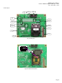
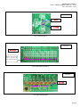
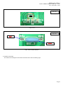
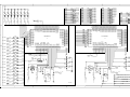
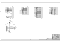
FEBL610Q178RB-01
LAPIS SEMICONDUCTOR CO., LTD.
Dec. 2012 (Rev. 1.00)
ML610Q178 Reference Board User's Manual
ML610Q178 Reference board is prepared by LAPIS SEMICONDUCTOR to have you study the operations of ML610Q178.
The board is arranged so that necessary components are mounted by you according to your purpose, then only minimum necessary
components are mounted on the board by LAPIS SEMICONDUCTOR for brief use of ML610Q178.
By using the board with "uEASE on-chip debug emulator" (hereinafter referred to "uEASE") and "free sample U8 Development Tools
CD-ROM" which is bundled in the package of uEASE not only Software development/debugging but also writing Flash ROM in the
devices are capable.
This board also works in stand alone mode with external power suppy without uEASE.
Before starting works with this board, read below carefully and understand notices.
1. The board features
Incorporates ML610Q178 or 100pin IC-Socket
Supports flash ROM programming and on-chip debugging (using TEST0 and TEST1_N pins)
High extendibility; Through-holes for your peripheral board are equipped with microcontroller pins
The power supply used can be selected ( uEASE or peripheral board )
Prepared the pad to mount parts ( parts necessary for microcontroller operation )
2. The board hardware specifications
Please refer to the reference schematics for detail on connections of each hardware parts.
Embedded
microcontroller
U1/U2(Mounting / IC-Socket): ML610Q178
・ UVDD、VSS: Input power supply pin
・ PWR: Jumper for input power supply switch
( 3pin pin-header and short pin )
・ XT_1/XT_2(Mounting / IC-Socket ): 32.768kHz oscillator
・ OSC_1/OSC_2(Mounting / IC-Socket): 8MHz oscillator
・ P20-P23,P90-P93: Light emitting diodes
Embedded parts
・ CNUE: Connector for on-chip debug emulator
( 14pin connector )
・ C1-C2/C10-C11(Mounting / IC-Socket): Capacitors for 32.768kHz oscillator ( 2pieces )
・ C3-C5/C12-C14(Mounting / IC-Socket): Capacitors for power supply ( 3pieces )
・ C6-C8/C15-C17(Mounting / IC-Socket): Capacitors for LCD external input voltage connection(3 pieces)
・ C9,C18-C19: Capacitors for input voltage ( 3pieces )
・ R1-R3/R4-R6(Mounting / IC-Socket): Resistance for LCD external input voltage connection(3 pieces)
・ R7-R10,R11-R14: Resistance for light emitting diodes (P20-P23,P90-P93)
・ PP1/PP4(Mounting / IC-Socket): Pads for LCD drive power supply
・ PP2-PP3/PP5-PP6(Mounting / IC-Socket): Land for P10, P11 terminal connection
Pads
for mounting
・ PP7-PP14: Land for light emitting diodes
・ AIN0-AIN15: Land for SA-ADC terminal connection
・ CN1-CN4: Pads for peripheral board connectors( 30pin×2、20pin×2、2.54mm pitch)
Other useful pads
・ VDD、VSS、UVDD、VREF、AIN0-AIN15
Operating voltage
・ VDD = +2.2V to +5.5V、VREF = +4.5V to +5.5V
Board size
・ 100.00 x 120.00 mm
Page1
FEBL610Q178RB-01
LAPIS SEMICONDUCTOR CO., LTD.
Dec. 2012 (Rev. 1.00)
3. Parts layout
CN1
PWR
CNUE
UVDD
VSS
XT_2
OSC_2
XT_1
OSC_1
CN4
VREF
U1
Device
U2
Socket
P90-P93
CN2
P20-P23
CN3
<fig.1 Parts layout>
L610Q178
XXXXXXXJ
1pin
<fig.2 The device set direction>
Page2
FEBL610Q178RB-01
LAPIS SEMICONDUCTOR CO., LTD.
Dec. 2012 (Rev. 1.00)
4. Notes on use
(1) The information contained herein can change without notice owing to product and/or technical improvements.
Before using the product, please make sure that the information being referred to is up-to-date.
(2) Before using this board, read carefully and understand the contents of the ML610Q178 user's manual and the uEASE user's
manual.
(3) The engineering sample of ML610Q178 might be mounted on the board.
Therefore, please confirm the characteristic finally by using MP of ML610Q178 and customer's mass production boards.
(4) LAPIS Semiconductor will not provide any support for this board, but the board can be exchanged with a new product only when it
has an initial failure.
(5) When you set a device to a reference board, please set, where the power is turned off. Moreover, when a reference board is a "
IC-socket", please set not to mistake direction of a device.
The direction of 1 pin is the right upper part direction, when a lid is opened. Please refer to figure 2.(about device set direction)
(6) When a power supply is inputted from the external, please input between check pin UVDD-VSS and set a PWR jumper to the USR
side.
(7) Notes when the PWR jumper is set to USR side and the uEASE is connected.
Turn on the power supply of the peripheral board after starting the uEASE.
Moreover, Stop the uEASE after turning off the power supply of the peripheral board.
(8) When the PWR jumper is set to the uE side, the ability to supply power of the uEASE is +3.3v/100mA.
(9) Notes when the RESET_N signal is prepared on the peripheral board side.
If you use the uEASE, open or set DVDD-level RESET_N signal pin (CN3_71pin).
(When you control a RESET_N signal by the peripheral board, add a jumper terminal etc. to it and change into an open state.)
(10) There is a possibility of short the circuit when using it on electro conductive so that the board may have the pattern on the solder
side. Therefore, please use the board on nonconductivity or put the protection parts on the solder side if necessary.
(11) When you use SA-ADC:
When you connect to AIN0-AIN15 on this board the target SA-ADC input and you do not input into it by CN2 course, please cut the
pattern of AIN0-AIN15 if needed and input from the hole of the way near a device. Please refer to figure 4. ( AIN0-AIN15 (SA-ADC))
VREF is connected with VDD by the jumper at the time of shipment. When you input arbitrary voltage, please change a VREF jumper
to the USER side and input VREF voltage from 1_CN6 pin (VREF_IN). Please refer to figure 3. ( VREF (SA-ADC))
(12) When you don’t use light emitting diodes:
P20-P23, P90-P93 can drive direct to light emitting diodes. P20-P23, P90-P93 are wired with light emitting diodes through PP7-PP14.
Please cut the land of the PP7-PP14 when you don’t use light emitting diodes, as shown in the fig.5.
(13) When driving LCD
The chip resistor of 2012 sizes can be mounted between VL3 to VDD (PP1 to PP4 pad). At the time of shipment, since VDD and VL3
short-circuit, please mount a chip resistor in PP1/PP4 if needed. Please refer to figure 6.( VL3 )
(14) When P10-P11 is used as general input ports
P10-P11 can change and use a 8MHz oscillation terminal and a general input port terminal. When you use it as a general input port
terminal, please remove an 8MHz oscillator and short-circuit PP2/PP5 and PP3/PP6, respectively.
Please refer to figure 7. ( P10,P11 8MHz oscillator )
Page3
FEBL610Q178RB-01
LAPIS SEMICONDUCTOR CO., LTD.
Dec. 2012 (Rev. 1.00)
Top View
Short
Cut LAND
<fig.3 VREF(SA-ADC)>
Top View
Cut Pattern
Please input directly
after a cut from the
hole of the side here.
<fig.4 AIN0-AIN15 (SA-ADC)>
Top View
Cut LAND
<fig.5 Light emitting diodes>
Page4
FEBL610Q178RB-01
LAPIS SEMICONDUCTOR CO., LTD.
Dec. 2012 (Rev. 1.00)
Top View
<fig.6 VL3>
Top View
Short
Remove
<fig.7 P10,P11 8MHz oscillator>
5. Reference schematics
The reference circuit diagram of this reference board is shown after the following page.
Page5
A
B
D
C
560
P20
1
PIN84
PIN83
PIN82
PIN81
PIN80
PIN79
PIN78
PIN77
PIN76
PIN75
PIN74
PIN73
PIN72
PIN71
2/1D
2/1D
2/1D
2/1D
2/2C
2/2C
2/2C
2/2C
2/2C
2/2C
2/2C
2/2C
2/2C
2/2C
OUT
OUT
OUT
OUT
P93/LED7
P92/LED6
P91/LED5
P90/LED4
OUT
OUT
OUT
OUT
IN
IN
IN
IN
IN
OUT
OUT
OUT
OUT
OUT
P23/LED3
P22/LED2
P21/LED1
P20/LED0
NMI
P03/INT3
P02/INT2
P01/INT1
P00/INT0
P43/TXD0
P42/RXD0
P41/SCL
P40/SDA
RESET_N
PIN70
PIN69
PIN68
PIN67
PIN66
PIN65
PIN64
PIN63
PIN62
PIN61
PIN60
PIN59
PIN58
PIN57
PIN56
PIN55
PIN54
PIN53
PIN52
PIN51
2/2C
2/2C
2/2C
2/2C
2/2C
2/2C
2/2C
2/2C
2/1C
2/1C
2/1C
2/1C
2/1C
2/1C
2/1C
2/1C
2/1C
2/1C
2/1C
2/1C
1 AIN11 2
2/2D
1
OSC_1
1
1 AIN4 2
PIN1
1/4D,2/3A
2
1/4C,2/2A
IN
P11/OSC1
1/4C,2/2A
IN
NMI
P03/INT3
P02/INT2
P01/INT1
P00/INT0
P43/TXD0
P42/RXD0
P41/SCL
P40/SDA
RESET_N
PF7/SEG39
PF6/SEG38
PF5/SEG37
PF4/SEG36
PF3/SEG35
PF2/SEG34
PF1/SEG33
PF0/SEG32
PE7/SEG31
PE6/SEG30
PE5/SEG29
PE4/SEG28
PE3/SEG27
PE2/SEG26
PE1/SEG25
PE0/SEG24
PD7/SEG23
PD6/SEG22
PD5/SEG21
PD4/SEG20
1
2
3
4
5
6
7
8
9
10
11
12
13
14
15
16
17
18
19
20
21
22
23
24
25
26
27
28
29
30
PP4 1
PIN6
2
200K
2 R4 1
200K
2 R5 1
1
VDDL
IN
VPP
B
C16
0.22UF
LAPIS Semiconductor Co., Ltd.
DVSS
DRAWN By
C
2
DVSS
TITLE
ML610Q178 Reference Board
APPLICATION
ML610Q178
DWG NO
QTS-11548
SHEET
1 of 2
1
A
1
2
2
P10/OSC0
IN
2
1
PIN[100:1]
DVSS
12PF C11
DVSS
1/4B,2/3A
XT_2
DVSS
2
PIN5
DVSS
2
DVSS
1
1 AIN0 2
PIN4
3
12PF C10
2/1A
1 AIN1 2
VPP
2
I/O
2/1A
C1
I/O
IN
1
0.22UF
2
PIN3
VDDL
1
1 AIN2 2
2
1
2/1A
1
DVSS
1UF C5
PIN2
12PF C2
1 AIN3 2
1/4D,2/3A
XT_1
2
P30/AIN0
2/1A
IN
1
C15
0.22UF
2
2/1A
3
1/4B,2/3A
1
PIN100
C8
10UF C13
1 2
1 AIN5 2
VDD
3
2
C14
0.22UF
OSC_2
2
10UF C12
2/2D
1
1
2
0.22UF
P11/OSC1
PIN99
1
P31/AIN1
2
PIN30
PIN29
PIN28
PIN27
C7
12PF
I/O
1
P36/LSCLK
P35/PWM5
P34/PWM4
P53/TXD1
P52/SOUT1
P51/SCK1
P50/SIN1
PIN50
PIN49
PIN48
PIN47
PIN46
PIN45
PIN44
PIN43
PIN42
PIN41
PIN40
PIN39
PIN38
PIN37
PIN36
PIN35
PIN34
PIN33
PIN32
PIN31
50
49
48
47
46
45
44
43
42
41
40
39
38
37
36
35
34
33
32
31
200K
2 R6 1
1
2
P32/AIN2
COM0
COM1
COM2
COM3
80
79
78
77
76
75
74
73
72
71
70
69
68
67
66
65
64
63
62
61
60
59
58
57
56
55
54
53
52
51
3
1
4
I/O
PD3/SEG19
PD2/SEG18
PD1/SEG17
PD0/SEG16
PC7/SEG15
PC6/SEG14
PC5/SEG13
PC4/SEG12
PC3/SEG11
PC2/SEG10
PC1/SEG9
PC0/SEG8
SEG7
SEG6
SEG5
SEG4
SEG3
SEG2
SEG1
SEG0
C6
0.22UF
VDD
DVSS
P33/AIN3
I/O
I/O
I/O
I/O
I/O
I/O
I/O
2
2
1
1
1
PP6
1 AIN6 2
OUT
OUT
OUT
OUT
2/2A
2/2A
2/1A
2/1A
2/1A
2/1A
2/1A
2
1
IN
PIN98
C17
2
VREF_IN
VDD
1UF
1 PP5
1 AIN7 2
VDD
C
2
USR
2/2D
U2
1/4B,2/2A
VREF
2/2D
2/2A
2/2A
2/2A
2/2A
PIN13
PIN12
PIN11
PIN10
PIN9
PIN8
PIN7
IC SOCKET
IN
2
2/1A
2
I/O
PIN97
1
P44/AIN4
2
1
10UF C4
I/O
1
C9
10UF C3
P45/AIN5
2/2D
AIN8
PIN30
PIN29
PIN28
PIN27
VDD
IN
I/O
1UF
2
P46/AIN6
I/O
I/O
IN
PIN14
PIN15
PIN96
1
P47/AIN7
I/O
1 AIN9 2
2/3A
2/3A
DVSS
P60/AIN8
I/O
PD3/SEG19
PD2/SEG18
PD1/SEG17
PD0/SEG16
PC7/SEG15
PC6/SEG14
PC5/SEG13
PC4/SEG12
PC3/SEG11
PC2/SEG10
PC1/SEG9
PC0/SEG8
SEG7
SEG6
SEG5
SEG4
SEG3
SEG2
SEG1
SEG0
PIN95
PP2
P61/AIN9
DVSS
DVSS
3
I/O
I/O
I/O
I/O
I/O
I/O
I/O
I/O
I/O
I/O
I/O
I/O
OUT
OUT
OUT
OUT
OUT
OUT
OUT
OUT
VDD
2
TEST0
TEST1_N
2/2D
P20/LED0
P21/LED1
P22/LED2
P23/LED3
VSS_85
P90/LED4
P91/LED5
P92/LED6
P93/LED7
P67/AIN15
P66/AIN14
P65/AIN13
P64/AIN12
P63/AIN11
P62/AIN10
P61/AIN9
P60/AIN8
P47/AIN7
P46/AIN6
P45/AIN5
PIN30
PIN29
PIN28
PIN27
1/4A,2/2A
AIN10
PIN94
2/2B
2/2B
2/2B
2/2B
2/2B
2/2B
2/2B
2/2B
2/2B
2/1B
2/1B
2/1B
2/1B
2/1B
2/1B
2/1B
2/1B
2/1B
2/1B
2/1B
PIN1
PIN2
PIN3
PIN4
PIN5
PIN6
PIN7
PIN8
PIN9
PIN10
PIN11
PIN12
PIN13
PIN14
PIN15
2/2D
PIN86
PIN87
PIN88
PIN89
PIN90
PIN91
PIN92
PIN93
PIN94
PIN95
PIN96
PIN97
PIN98
PIN99
PIN100
P10/OSC0
I/O
DVSS
81
82
83
84
85
86
87
88
89
90
91
92
93
94
95
96
97
98
99
100
PP1 1
P62/AIN10
PIN93
2
I/O
1 AIN12 2
2/2D
200K
2 R1 1
P63/AIN11
PIN92
200K
2 R2 1
I/O
1 AIN13 2
PIN81
PIN82
PIN83
PIN84
PIN50
PIN49
PIN48
PIN47
PIN46
PIN45
PIN44
PIN43
PIN42
PIN41
PIN40
PIN39
PIN38
PIN37
PIN36
PIN35
PIN34
PIN33
PIN32
PIN31
200K
2 R3 1
P64/AIN12
2/1D
U1
PIN6
I/O
PIN91
50
49
48
47
46
45
44
43
42
41
40
39
38
37
36
35
34
33
32
31
1
2
3
4
5
6
7
8
9
10
11
12
13
14
15
16
17
18
19
20
21
22
23
24
25
26
27
28
29
30
P65/AIN13
2
AIN14
ML610Q178
PIN1
PIN2
PIN3
PIN4
PIN5
PIN6
PIN7
PIN8
PIN9
PIN10
PIN11
PIN12
PIN13
PIN14
PIN15
I/O
1
PIN90
PIN91
PIN92
PIN93
PIN94
PIN95
PIN96
PIN97
PIN98
PIN99
PIN100
2
P66/AIN14
2/1D
PIN90
PP3
I/O
1 AIN15 2
PD3/SEG19
PD2/SEG18
PD1/SEG17
PD0/SEG16
PC7/SEG15
PC6/SEG14
PC5/SEG13
PC4/SEG12
PC3/SEG11
PC2/SEG10
PC1/SEG9
PC0/SEG8
SEG7
SEG6
SEG5
SEG4
SEG3
SEG2
SEG1
SEG0
1
P67/AIN15
2/1D
NMI
P03/INT3
P02/INT2
P01/INT1
P00/INT0
P43/TXD0
P42/RXD0
P41/SCL
P40/SDA
RESET_N
PF7/SEG39
PF6/SEG38
PF5/SEG37
PF4/SEG36
PF3/SEG35
PF2/SEG34
PF1/SEG33
PF0/SEG32
PE7/SEG31
PE6/SEG30
PE5/SEG29
PE4/SEG28
PE3/SEG27
PE2/SEG26
PE1/SEG25
PE0/SEG24
PD7/SEG23
PD6/SEG22
PD5/SEG21
PD4/SEG20
80
79
78
77
76
75
74
73
72
71
70
69
68
67
66
65
64
63
62
61
60
59
58
57
56
55
54
53
52
51
2
P20/LED0
P21/LED1
P22/LED2
P23/LED3
VSS_85
P90/LED4
P91/LED5
P92/LED6
P93/LED7
P67/AIN15
P66/AIN14
P65/AIN13
P64/AIN12
P63/AIN11
P62/AIN10
P61/AIN9
P60/AIN8
P47/AIN7
P46/AIN6
P45/AIN5
P44/AIN4
P33/AIN3
P32/AIN2
P31/AIN1
P30/AIN0
VREF
P50/SIN1
P51/SCK1
P52/SOUT1
P53/TXD1
P34/PWM4
P35/PWM5
P36/LSCLK
TEST0
TEST1_N
P10/OSC0
P11/OSC1
VSS_18
VDD
VDDL
XT0
XT1
VPP
VL1
VL2
VL3
COM3
COM2
COM1
COM0
81
82
83
84
85
86
87
88
89
90
91
92
93
94
95
96
97
98
99
100
PIN50
PIN49
PIN48
PIN47
PIN46
PIN45
PIN44
PIN43
PIN42
PIN41
PIN40
PIN39
PIN38
PIN37
PIN36
PIN35
PIN34
PIN33
PIN32
PIN31
PF7/SEG39
PF6/SEG38
PF5/SEG37
PF4/SEG36
PF3/SEG35
PF2/SEG34
PF1/SEG33
PF0/SEG32
PE7/SEG31
PE6/SEG30
PE5/SEG29
PE4/SEG28
PE3/SEG27
PE2/SEG26
PE1/SEG25
PE0/SEG24
PD7/SEG23
PD6/SEG22
PD5/SEG21
PD4/SEG20
I/O
I/O
I/O
I/O
I/O
I/O
I/O
I/O
I/O
I/O
I/O
I/O
OUT
OUT
OUT
OUT
OUT
OUT
OUT
OUT
PIN80
PIN79
PIN78
PIN77
PIN76
PIN75
PIN74
PIN73
PIN72
PIN71
PIN70
PIN69
PIN68
PIN67
PIN66
PIN65
PIN64
PIN63
PIN62
PIN61
PIN60
PIN59
PIN58
PIN57
PIN56
PIN55
PIN54
PIN53
PIN52
PIN51
C18
2.2UF
2/1D
2/1D
2/1D
2/1D
PIN80
PIN79
PIN78
PIN77
PIN76
PIN75
PIN74
PIN73
PIN72
PIN71
PIN70
PIN69
PIN68
PIN67
PIN66
PIN65
PIN64
PIN63
PIN62
PIN61
PIN60
PIN59
PIN58
PIN57
PIN56
PIN55
PIN54
PIN53
PIN52
PIN51
PIN71
PP7
PIN81 1
PIN87
PIN86
PIN84
PIN83
PIN82
PIN81
2
PIN89
PIN88
PIN87
PIN86
P44/AIN4
P33/AIN3
P32/AIN2
P31/AIN1
P30/AIN0
VREF
P50/SIN1
P51/SCK1
P52/SOUT1
P53/TXD1
P34/PWM4
P35/PWM5
P36/LSCLK
TEST0
TEST1_N
P10/OSC0
P11/OSC1
VSS_18
VDD
VDDL
XT0
XT1
VPP
VL1
VL2
VL3
COM3
COM2
COM1
COM0
560
P21
LED
2 2
1
1
2 2
1 R7 2
560
1 R8 2
P22
LED
PP8
PIN82 1
P23
LED
2
1
R9 2
1
560
PIN84 1
PIN89
PIN88
PP9
PIN83 1
560
1R10 2
P90
LED
2 2
1
PP10
P91
1R11 2
560
PIN87 1
PP11 2 LED
2
1
PIN86 1
560
1R13 2
1R12 2
P92
LED
2 2
1
PP12
DVSS
P93
PP13 2 2 LED 1
PIN88 1
1
PP14 2 2 LED 1
PIN89 1
1R14 2
560
VDD
D
REV
1.00
4
A
B
CN1
CN30P
1
P44/AIN4
P33/AIN3
P32/AIN2
P31/AIN1
P30/AIN0
VREF_IN
P50/SIN1
P51/SCK1
P52/SOUT1
P53/TXD1
P34/PWM4
P35/PWM5
P36/LSCLK
P10/OSC0
P11/OSC1
I/O
I/O
I/O
I/O
I/O
IN
I/O
I/O
I/O
I/O
I/O
I/O
I/O
1/3B
1/3B
1/3B
1/3B
1/3B
1/3B
1/3B
1/3B
1/3B
1/3B
1/3B
1/3B
1/3B
PIN7
PIN8
PIN9
PIN10
PIN11
PIN12
PIN13
(NC)
(NC)
1/4C,1/4A
1/4C,1/4B
IN
IN
2
COM3
COM2
COM1
COM0
PIN1
PIN2
PIN3
PIN4
PIN5
(NC)
(NC)
(NC)
(NC)
(NC)
(NC)
(NC)
PIN27
PIN28
PIN29
PIN30
1/3B
1/3B
1/3B
1/3B
OUT
OUT
OUT
OUT
D
C
CN3
CN30P-1
CN2
CN20P-1
1
2
3
4
5
6
7
8
9
10
11
12
13
14
15
16
17
18
19
20
21
22
23
24
25
26
27
28
29
30
SEG0
SEG1
SEG2
SEG3
SEG4
SEG5
SEG6
SEG7
PC0/SEG8
PC1/SEG9
PC2/SEG10
PC3/SEG11
PC4/SEG12
PC5/SEG13
PC6/SEG14
PC7/SEG15
PD0/SEG16
PD1/SEG17
PD2/SEG18
PD3/SEG19
OUT
OUT
OUT
OUT
OUT
OUT
OUT
OUT
I/O
I/O
I/O
I/O
I/O
I/O
I/O
I/O
I/O
I/O
I/O
I/O
1/1D
1/1D
1/1D
1/1D
1/1D
1/1D
1/1D
1/1D
1/1D
1/1D
1/1D
1/1D
1/1D
1/1D
1/1D
1/1D
1/1D
1/1D
1/1D
1/1D
PIN31
PIN32
PIN33
PIN34
PIN35
PIN36
PIN37
PIN38
PIN39
PIN40
PIN41
PIN42
PIN43
PIN44
PIN45
PIN46
PIN47
PIN48
PIN49
PIN50
31
32
33
34
35
36
37
38
39
40
41
42
43
44
45
46
47
48
49
50
PD4/SEG20
PD5/SEG21
PD6/SEG22
PD7/SEG23
PE0/SEG24
PE1/SEG25
PE2/SEG26
PE3/SEG27
PE4/SEG28
PE5/SEG29
PE6/SEG30
PE7/SEG31
PF0/SEG32
PF1/SEG33
PF2/SEG34
PF3/SEG35
PF4/SEG36
PF5/SEG37
PF6/SEG38
PF7/SEG39
RESET_N
P40/SDA
P41/SCL
P42/RXD0
P43/TXD0
P00/INT0
P01/INT1
P02/INT2
P03/INT3
NMI
I/O
I/O
I/O
I/O
I/O
I/O
I/O
I/O
I/O
I/O
I/O
I/O
I/O
I/O
I/O
I/O
I/O
I/O
I/O
I/O
IN
I/O
I/O
I/O
I/O
IN
IN
IN
IN
IN
1/1C
1/1C
1/1C
1/1C
1/1C
1/1C
1/1C
1/1C
1/1C
1/1C
1/1C
1/1C
1/1C
1/1C
1/1C
1/1C
1/1C
1/1C
1/1C
1/1C
1/3B
1/3B
1/3B
1/3B
1/3B
1/3B
1/3B
1/3B
1/3B
1/3B
PIN51
PIN52
PIN53
PIN54
PIN55
PIN56
PIN57
PIN58
PIN59
PIN60
PIN61
PIN62
PIN63
PIN64
PIN65
PIN66
PIN67
PIN68
PIN69
PIN70
PIN71
PIN72
PIN73
PIN74
PIN75
PIN76
PIN77
PIN78
PIN79
PIN80
CN4
CN20P-2
51
52
53
54
55
56
57
58
59
60
61
62
63
64
65
66
67
68
69
70
71
72
73
74
75
76
77
78
79
80
P20/LED0
P21/LED1
P22/LED2
P23/LED3
OUT
OUT
OUT
OUT
P90/LED4
P91/LED5
P92/LED6
P93/LED7
P67/AIN15
P66/AIN14
P65/AIN13
P64/AIN12
P63/AIN11
P62/AIN10
P61/AIN9
P60/AIN8
P47/AIN7
P46/AIN6
P45/AIN5
OUT
OUT
OUT
OUT
I/O
I/O
I/O
I/O
I/O
I/O
I/O
I/O
I/O
I/O
I/O
1
81
82
83
84
85
PIN86 86
PIN87 87
PIN88 88
PIN89 89
PIN90 90
PIN91 91
PIN92 92
PIN93 93
PIN94 94
PIN95 95
PIN96 96
PIN97 97
PIN98 98
PIN99 99
PIN100100
1/3B
1/3B
1/3B
1/3B
PIN81
PIN82
PIN83
PIN84
1/3B
1/3B
1/3B
1/3B
1/2A
1/2A
1/2A
1/3A
1/2A
1/2A
1/2A
1/2A
1/2A
1/2A
1/2A
DVSS
2
DVSS
1
uE
2
PWR
VDD
C
J1
USR
A2-3PA-2_54DSA
1
3
UVDD
1
VDD
CNUE
CN14P
3
3
1
2
3
4
5
6
7
8
9
10
11
12
13
14
1/4D,1/4B
PIN23
1/3B
PIN15
1/3B
PIN14
1/4B,1/4D
PIN20
IN
VPP
IN
TEST1_N
I/O
IN
TEST0
VDDL
1
VSS
DVSS
LAPIS Semiconductor Co., Ltd.
TITLE
4
ML610Q178 Reference Board
APPLICATION
ML610Q178
DWG NO
DRAWN By
A
B
C
QTS-11548
SHEET
2 of 2
D
REV
1.00
4