1
BDV11 bus
terminator,
bootstrap, and
diagnostic ROM
technical manual
BDV11 bus
terminator,
bootstrap, and
diagnostic ROM
technical manual
EK-BDV11-TM-001
digital equipment corporation • maynard, massachusetts
1st Edition, March 1978
Copyright
©
1978 by Digital Equipment Corporation
The materIal in this manual is for informational
purposes and is subject to change without notice.
Digital Equipment Corporation assumes no responsibility for any errors which may appear in this
manual.
Printed in U.s.A.
This document was set on DIGITAL's DECset-8000
computerized typesetting system.
The following are trademarks of Digital Equipment
Corporation, Maynard, Massachusetts:
DEC
DECCOMM
DECsyste'm-lO
DECSYSTEM·20
DEC tape
DEC US
DIGITAL
MASSBUS
PDP
RSTS
TYPESET-8
TYPESET·!!
UNIBUS
CONTENTS
Page
CHAPTER 1
INTRODUCTION
1.1
1.2
1.3
1.4
MANUAL SCOPE ......... ;.................................................................................... 1-1
GENERAL DESCRIPTION ............................................................................... 1-1
BDVII SPECIFICATIONS ................................................................................. 1-3
RELATED PUBLICATIONS ............................................................................. 1-3
CHAPTER 2
INSTALLATION
2.1
2.2
2.3
2.4
SCOPE ................................................................................................................ 2-1
PRELIMINARY STEP ....................................................................................... 2-1
INSTALLING THE MODULE IN A BACKPLANE ......................................... 2-1
MODULE PIN-OUTS AND LOGIC DRAWINGS ........................................... 2-3
CHAPTER 3
OPERATION
3.1
3.1.1
3.1.2
3.1.3
3.2
SWITCHES AND INDICATORS ...................................................................... );. 1
POWER OK LED (D6), HALT/ENABLE Switch (SI), RESTART
Switch (S2), and BEVNT L Switch (Section 5 of E21) .................................... 3-1
Diagnostic/Bootstrap Switches .................................................................... 3-1
Diagnostic Light Display .............................................................................. 3-1
HARDWARE REGISTERS ............................................................................... 3-1
CHAPTER 4
TECHNICAL DESCRIPTION
4.1
4.2
4.3
4.4
4.5
4.6
4.7
4.8
4.9
4.10
4.11
ADDRESSING ROM ON THE BDVII MODULE .......................................... .4-1
BDVII BLOCK DIAGRAM ............................................................................... 4-4
TRANSCEIVER/SWITCH REGISTER LOGIC ............................................... 4-6
CONTROL LOGIC ............................................................................................. 4-8
POWER-UP LOGIC ......................................................................................... 4-12
ROM ADDRESS SELECTION LOGIC ........................................................... 4-12
SOCKET SELECTION LOGIC ....................................................................... .4-16
ROM SOCKETS LOGIC .................................................................................. 4-19
BEVNT LOGIC ................................................................................................. 4-19
DISPLi~'''Y LOG!C ............................................................................................. 4-19
READ/WRITE REGISTER LOGIC ............................................................... .4-23
APPENDIX A
ROM SPECIFICATIONS
iii
FIGURES
Figure No.
I-I
2-1
3-1
3-2
4-1
4-2
4-3
4-4
4-5
4-6
4-7
4-8
4-9
4-10
4-11
4-12
4-13
Title
Page
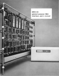
BDYII Module .................................................................................................... 1-2
Insertion and Removal of Modules Having Extractor-Type Handles .................... 2-2
BDYII Switches and Indicators ........................................................................... 3-2
Diagnostic Light Display ...................................................................................... 3-2
BDYII Block Diagram ........................................................................................ 4-5
Transceiver and Switch Register Logic, Bits 0-3 .................................................. .4-7
Control Logic ....................................................................................................... 4-9
Operation Sequence, DATO Cycle ..................................................................... 4-11
Power-Up Logic ................................................................................................. 4-13
ROM Address Selection Logic ........................................................................... .4-14
Address Bit Selection .......................................................................................... 4-15
Socket Selection Logic ........................................................................................ 4-17
Logic Block Diagram, ROM Sockets .................................................................. 4-20
System ROM Jumpers ........................................................................................ 4-21
BEVNT Logic .................................................................................................... 4-22
Display Logic/LEDs D I-D4 ............................................................................. .4-22
Read/Write Register Logic ................................................................................. 4-23
TABLES
Table No.
I-I
2-1
3-1
3-2
4-1
4-2
4-3
4-4
4-5
4-6
4-7
4-8
Title
Page
BDYII Specifications ........................................................................................... 1-3
BDYII Bus Pin-Outs ............................................................................................ 2-3
Functions of the Maintenance Aids ...................................................................... 3-3
BDYII Hardware Registers ................................................................................. 3-4
BDY11 Bus Addresses/PCR Pages ...................................................................... .4-2
Functions of ROM Sockets .................................................................................. 4-2
peR Contents/Page Relationship, Pages 0-17 ...................................................... 4-3
PCR Contents, Pages 20-57, 200-377 .................................................................. .4-4
DC004 Select Outputs ........................................................................................ 4-1 0
DC004 Protocol Signals ...................................................................................... 4-1 0
DC004 Byte Signals ............................................................................................ 4-1 0
BD Y II Selection Signals/Sockets ...................................................................... .4-18
IV
CHAPTER 1
INTRODUCTION
1.1 MANUAL SCOPE
The BDVII is an LSI-II bus option that provides both 120-ohm terminations for LSI-II bus signal
lines and diagnostic aids that help a user to determine the operating condition of his system. The
BDVII module can be equipped with a variety of read-only memories (ROMs) to provide the user
with bootstrap and additional diagnostic capabilities; in such a case, a new option designation is
assigned, e.g., BDVII-AA.
This manual gives a technical description of only the BDVII module. Each variation of the BDVII is
described in a user manual that pertains only to that variation. The reader should be familiar with the
LSI-II microcomputer and its peripheral equipment. The necessary information can be obtained from
the 1977-1978 Microcomputer Handbook* published by DIGITAL.
1.2 GENERAL DESCRIPTION
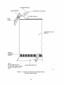
The BDVII logic components are mounted on a 26.7 X 21.6 cm (10.5 X 8.5 in) quad-height printed
circuit board (Figure 1-1) that can be inserted in any LSI-II bus quad backplane. Physical space on the
module is reserved by DIGITAL for 4K words of ROM; this ROM space contains diagnostic and
bootstrap programs for a number of system components. Furthermore, user-available space is furnished on the module for 2K words of eraseable, programmable ROM (EPROM) and 16K words of
ROM or EPROM. This 18K of user ROM can be executed directly or loaded into ROM for later
execution; all ROM is mapped into only 256 words of LSI-II I/O address space.
The BDVl1 contains switches that permit the user to choose diagnostic and bootstrap programs for
execution and a diagnostic light display that indicates failures in these programs. In addition, the
BDVII module is equipped with a green LED that monitors dc power, two test points for the dc
power, a HALT/ENABLE switch that allows the user to force the CPU into the halt mode, and a
REST ART switch that enables the user to re-boot the system. All of these controls are edge-mounted.
A switch mounted in the interior of the module permits control of the LSIp 11 line-time clock (LTC)
function.
*See Paragraph 1.4 for ordering information.
1-1
9036·3BW·A0043
Figure 1-1
BDVII Module
1-2
1.3 BDVll SPECiFiCATiONS
The specifications listed in Table 1-1 are for informational purposes only and are subject to change
without notice.
Tabie 1-1
BDVll Specifications
Specification
Item
Physical Characteristics
Length (without handles)
Height (without handles)
Depth
26.7 cm (10.5 in)
21.6 cm (8.5 in)
1.27 cm (0.5 in)
Electrical Characteristics
BDVl1 Module Type
M8012
Power Requirements
+5 Vdc @ 1.6 A (max)
+ 12 Vdc @ 0.07 A (max)
LSI-II Bus Loading
2 ac unit loads
Environmental Requirements
Operating Temperature*
Operating Humidity
*
10-95%, with a maximum wet bulb temperature of 32 0 C (90 0 F)
and a minimum dew point of 2 0 C (36 0 F)
The maximum allowable operating temperature is based on operation at sea level, i.e., at 760 mm Hg (29.92 in
Hg); maximum allowable operating temperature must be reduced by a factor of 1.8 0 C/1000 m (1.0 0 F 11000
ft) for operation at higher altitudes.
1.4 RELATED PUBLICATIONS
Information that is useful to the BDVl1 user can be found in the following DIGITAL publications.
Publication
Document Number
Remarks
BA I1-N Mounting Box
Technical Manual
EK~BAI1N-TM-001
In microfiche library; also
available in hard copy
BAI1-N Mounting Box
User's Guide
EK-BAIIN-UG-OOI
A vailable in hard copy
Microcomputer Handbook,
1977-1978 (2nd Edition)
EB-07948-53/77
A vailable in hard copy
PD P-l1 Software Handbook
EB-08127 -20 /70
A vail able in hard copy
1-3
For information concerning microfiche libraries, contact:
Digital Equipment Corporation
132 Parker St.
Maynard, MA 01754
Attn:
Micropublishing Group
(PK3-2/T 12)
Hard copy documents can be ordered from:
Digital Equipment Corporation
444 Whitney St.
Northboro, MA 01531
Attn:
Communications Services (NR2/M 15)
Customer Services Section
1-4
CHAPTER 2
INSTALLATION
2.1 SCOPE
This chapter describes the steps to take before installing the BDV11 in a backplane and tells how and
where to install the module. Detailed information concerning the installation of LSI-ll system components can be found in the reference pUblications listed in Paragraph 1.4. Refer to the specific
BDVlI-variation user manual for procedures that check for correct system operation after the installation.
2.2 PRELiMiNARY STEP
A number of switches on the module must be set before the module is inserted in the backplane. The
diagnostic/bootstrap switches are used for maintenance and system configuration; the BEVNT switch
is used to select the mode of control of the LSI-II bus BEVNT signal. The location of these switches is
shown in Figure 3-1; their operation is described in Paragraphs 3.1.1 and 3.1.2. Ensure that the
switches are in the desired positions before installing the module.
2.3 INSTALLING THE MODULE IN A BACKPLANE
The BDVII can be inserted in any LSI-II quad backplane. In multiple-backplane systems the module
must be inserted in the last backplane of the system. When inserting the module, make sure the power
is turned off. Connector A of the module is inserted in connector A of the backplane (connector A on
the module is the right-most connector when viewing the component side of the module with the
connector fingers pointing down; connector A on the backplane is on the left side when viewing the
slot side of the backplane). The LSI-II bus signals will appear on module connectors A and B.
The BDVII is equipped with metal extractor-type handles that facilitate module insertion and removal. When inserting such a module into the backplane, begin by sliding the module, component side
up, into the card guides. Slide the module all the way in and just start the module connector fingers
into the backplane connectors. Fit the prongs of the handles into the holes in the card frame (Figure 21). Press in on both handles simultaneously to fully insert the fingers in the backplane connector.
To remove the module, pull both handles out simultaneously until the prongs of the handle are clear of
the holes in the card frame. The module fingers will now be nearly free of the backplane connector and
the module can be removed easily.
CAUTION
The module and/ or the backplane assembly might be
damaged if the module is inserted or removed with
the power on or if the module is inserted upside down.
2-1
CARD
FRAM E--__../
COMPONENT SIDE OF
~MODULE
MODULE
CONNECTORFINGERS
NOTE:
VIEW IS FROM THE TOP
OF THE CARD FRAME. LOOKING
TOWARD THE REAR OF THE
UNIT.
BACKPLANE CONNECTOR
MA-1339
Figure 2-1
Insertion and Removal of Modules Having
Extractor-Type Handles
2-2
2.4 l\10DULE PIN-OUTS AND LOGIC DRA\VINGS
The M8012 print set includes logic drawings. Signal names in the iogic drawings have the following
form.
SOURCE
POLi\RITY
SOURCE indicates the particular sheet of the drawings where the signal originates. SIGNAL NAME
is the proper name of the signal; the names used in the drawings are also used in this manual. POLARITY is either H or L to indicate the voltage level of the signal when asserted: H ~ +3 V; L ~ Ground.
As an example, the signal SH2 REG L originates on sheet 2 of the drawings and means when REG is
true, this signal is at approximately ground level.
LSI-II bus signal lines do not carry a SOURCE indicator. These names represent a bidirectional wireORed bus.
a result, multiple sources for a particular bus signal exist. T-he LSI-II bus signal names
begin with a "B" for "bussed." The bus pin-outs for the BDVII are listed in Table 2-1.
As
Table 2-1
BDVll Bus Pin-Outs
Mnemonic
Pin
Mnemonic
Pin
+5
+5
+12
BBS7L
BDALOL
BDALIL
BDAL2L
BDAL3L
BDAL4L
BDAL5L
BDAL6L
BDAL7L
AA2
BA2
AD2
AP2
AU2
AV2
BE2
BF2
BH2
BJ2
BK2
BL2
BIAKI L*
BIAK 0 L
BINIT L
BDMGI L*
BDMGO L*
BIRQL
BRPLYL
BSYNCL
BDCOKH
GND
GND
GND
AM2
AN2
AT2
AR2
AS2
AL2
AF2
AJ2
BAI
AC2
ATI
BC2
BDAL8L
BM2
GND
BTl
BDAL9L
BDAL 10 L
BDAL II L
BDAL 12 L
BDAL 13 L
BDAL 14 L
BDALI5L
BDINL
BDOUTL
BHALT L
BN2
BP2
BR2
BS2
BT2
BU2
BV2
AH2
AE2
API
MSPARE A (-12 V)
AKlt
ALI
BKlt
BLI
BCI
BDI
BEl
BFI
BHI
MSPARE B(EXT R CLK)
SSPARE4
SSPARE 5
SSPARE6
SSPARE 7
SSP ARE 8 (EXT T CLK)
* These signals are not bussed; they are daisy-chained.
t This jumper is wired on the backplane.
2-3
:J
:J
CHAPTER 3·
OPERATION
3.1 SWITCHES AND INDICATORS
There are two lever switches (S 1 and S2) and five LEDs (D 1-D4 and D6) mounted on the front edge of
the BDVll module, and two dip-socket switch units (E15 and E21) mounted on the interior of the
module. These components are identified in Figure 3-1 and described in the following paragraphs.
3.1.1 POWER OK LED (D6), HALT /ENABLE Switch (SI), RESTART Switch (S2), and BEVNT L
Switch (Section 5 of E21)
These components are maintenance aids. Table 3-1 describes the function of each component.
3.1.2 Diagnostic/Bootstrap Switches
The dip-socket switch units, E15 and E21, are used with BDVll variations. The switches, except
switch 5 of E21, allow the user to select diagnostic programs and/or a bootstrap program that run
automatically when power is turned on or when the system is re-booted. (Refer to the appropriate user
manual for details.) The 12 individual switches comprise the switch register, which can be read at bus
address 177524. (Table 3-2 includes a description of this register and its function in the BDVll.)
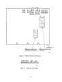
3.1.3 Diagnostic Light Display
The diagnostic light display is used primarily with BDVll variations. In these applications, the display
indicates the area of failure of a dial!nostic or bootstrao. Figure 3-2 illustrates the left front edge of the
module (as viewed from the rear ~f the mounting box), ~howing the five LEDs that comprise the
display. D6 is the POWER OK LED, which is lighted when the +12 Vdc and +5 Vdc supplies are
operating correctly and which indicates the octal point for the display value. Refer to the appropriate
user manual for information.
3.2 HARDWARE REGISTERS
The BDVl1 contains six hardware registers. These are listed in Table 3-2, together with a functional
description of each.
3-1
HALT
J3 J2
+-+
ENABLE
J1
DO
00000
S2
0
HALT/
ENABLE
I
SWITrH
""" I
RESTART
SWITCH
D1D2D3D6D4
OFF
ON
--,
__ 2
__ 3
__ 4
__ 5
__ 6
__ 7
__ 8
OFF
ON
__ 1
__ 2
__ 3
__ 4
E2i
Ei5
/
(DIAGNOSTIC/BOOTSTRAP
SWITCHES. BEVNT SWITCH)
\
(DIAGNOSTIC/BOOTSTRAP
SWITCHES)
MA-1340
Figure 3-1
BDVII Switches and Indicators
S2
D4 D6 D3 D2 D1
, 00000 lel
MA-1341
Figure 3-2
Diagnostic Light Display
3-2
Table 3-1
Functions of the Maintenance Aids
Component
Function
POWER OK LED
This green LED is lighted when the + 12 Vdc supply voltage is greater
than + 10 V and the + 5 V dc supply voltage is greater than +4 V. The
+ 12 Vdc voltage and the +5 Vdc voltage can be measured at the tip
jacks as indicated below. (Both J2 and J3 have a 560-ohm resistor in
series to prevent damage from a short circuit; use at least a 20,000ohmjV meter to measure the voltage.)
Jack
,"-,UIUI
Voltage
Jl
J2
J3
Black
Red
Purple
Ground
+5Vdc
+12 Vdc
,....~1~_
Secondariiy, the LED indicates the octal point for the diagnostic
light display (Paragraph 3.1.3).
HALT jENABLE Switch
When this switch is in the ENABLE position, the LSI-II CPU can
operate under program control. If the switch is placed in the HALT
position, the CPU enters the halt mode and responds to console
ODT commands. While in the halt mode, the CPU can execute single
instructions, facilitating maintenance of the system. Program control
is re-established by returning the switch to the ENABLE position
and entering a "P" command at the console terminal (providing the
contents of register R 7 were not changed). Refer to Chapter 2 of the
1977-1978 Microcomputer Handbook for a description of console
ODT command usage.
RESTART Switch
When the REST ART switch is cycled, i.e., moved from one side to
the other and back, the CPU automatically carries out a power-up
sequence. Thus, the system can be re-booted at any time for maintenance purposes.
BEVNT L Switch
Contact 5 of dip-socket switch E21 is the BEVNT L switch. When the
switch is off (open) the LSI-II bus BEVNT L signal can be controlled
by the power supply-generated LTC signal. When the switch is on
(closed), the LTC function is program-controlled; i.e., a single-bit,
write-only register in the logic (address 177546, bit 6) clamps BEVNT
L low when the register is cleared. (The register is automatically
cleared when the power is turned on or when the RESTART switch is
cycled.) The KWII-L line-time clock option also uses bit 6 as the
enable bit.
3-3
Table 3-2
BDVll Hardware Registers
Register
Size
Function
Bus Address
Page Control Register
(PCR)
16 bits
Controls mapping of ROM
pages into physical ROM addresses. Cleared when power is
turned on or when RESTART
switch is activated.
177520 (word or byte addressable; can be read or
written)
Read/Write Register
16 bits
Maintenance register used for diagnostics. Cleared when power is
turned on or when REST AR T
switch is activated.
177522 (word or byte addressable; can be read or
written)
Switch Register
12 bits
Used for maintenance and system configuration (selects diagnostic and/or bootstrap
programs for execution). Bits
0-11 of the register (corresponding to E15-1 through E15-8 and
E21-1 through E21-4, respectively) are associated with BDAL
<0: 11 > L, respectively; when an
individual switch of the register
is closed (on), the corresponding
BDAL signal is low (1).
177524 (read-only register)
Display Register
4 bits
Controls the diagnostic light display. Bits 0-3 of the register control LEDs DI-D4~ respectively;
when a bit is set, the corresponding LED is off. Cleared (all lights
on) when power is turned on or
when RESTART switch is activated.
177524 (word or byte addressa ble; write-only register)
BEVNT Register
1 bit
When cleared, this register
clamps the BEVNT signal low (if
the BEVNT switch is closed).
This action permits program
control of the LSI-II line-time
clock (LTC) function. Register
cleared when power is turned on
or when REST AR T switch is activated.
177546 (word or byte addressable; write-only register)
3-4
CHAPTER 4
TECHNICAL DESCRIPTION
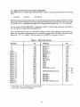
4.1 ADDRESSING ROM ON THE BDVll MODULE
A block of 256 LSI-II bus addresses is reserved for use in addressing ROM locations on the BDV11
module. This block resides in the upper 4K address bank (28K-32K), which is normally used for
peripheral-device addressing, and consists of byte addresses 173000-173776 (512 byte addresses correspond to 256 word addresses in the LSI-II addressing scheme).
The BDV11 logic enables all 2048 locations in a selected 2K ROM (or 1024 locations in a lK ROl\1) to
be addressed by just these 256 bus addresses. The logic includes a page control register (PCR) at bus
address 177520; the contents of this read/write register determine the specific ROM location that is
accessed when one of the 256 bus addresses is placed on the BDAL lines. The PCR is loaded with
"page" information, i.e., the PCR contents point to one of 16 (or one of 8) 128-word pages in the
seiected ROM 06 pages X 128 words = 2048 words). To illustrate, if the peR contents represent
pages 0 and 1, bus addresses 173000-173776 access ROM locations 0000-0377; if the PCR contents
represent pages 10 and 11, bus addresses 173000-173776 access ROM locations 2000-2377. Table 4-1
relates bus addresses, PCR pages, and ROM locations.
At the top of each column of PCR pages in Table 4-1 appear two circuit component designations;
column 1, for example, is headed by E53/E48. These designations represent the ROMs and EPROMs
that one might find on a BDV11 module. For instance, the BDV11-AA is supplied with 2K words of
diagnostic ROM. The ROM inserted in socket XE53 supplies the high byte (bits 8-15) of these 2K
words, while the ROM inserted in socket XE48 supplies the low byte (bits 0-7). To access the BDV11
diagnostic ROlVi locations, the user must load the peR with the pages in column 1; thus, when 12 and
13, for example, are loaded in the PCR, diagnostic ROM locations 2400-2777 can be addressed by the
LSI-II BDAL signals. Another variation of the BDV11 could have 1K-word EPROMs inserted in
sockets XE57/XE40 (E57 supplies the high byte, while E40 supplies the low byte). To access these
EPROM locations, the user would load the PCR with pages in column 3; thus, with 44 and 45 in the
PCR, EPROM locations 1000-1377 are accessible.
As Table 4-1 implies, the PCR pages are assigned to specific module ROM sockets. Furthermore, the
sockets are assigned specific kinds of ROMs, as indicated in Table 4-2; e.g., the diagnostic/bootstrap
ROM can occupy only sockets XE53 and XE48. Thus, a specific ROM can be addressed only when the
PCR contains the page or pages assigned to the socket that the ROM occupies. To illustrate, if 2K
ROMs are inserted in sockets E39 and E50, they can be addressed only when the PCR contains pages
360-377. The page/socket assignments indicated in Table 4-1 apply to the BDV11 module shipped by
DIGITAL. There are eight locations on the BDV11 printed circuit board in which jumpers are inserted
selectively to achieve these assignments. It is possible to change the factory arrangement of these
jumpers; by doing so, the user can cause the CPU to execute instructions directly from a ROM or
EPROM of the user's choice when power is turned on, rather than from the diagnostic ROMs. Paragraph 4.7 describes the jumpers in detail and shows how they can be rearranged.
4-1
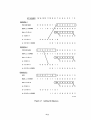
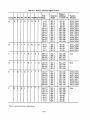
Table 4-1
BnVll Bus Addresses/PCR Pages
PCRPages
Bus Address
ROM
E53/ E58/ E57/ E52/ E54/ E59/ E60/ E55/ E51/ E47/ E43/ E39/ Location
E48 E44 E40 E36 E49 E45 E41 E37 E38 E42 E46 E50 Accessed
173000-173376
173400-173777
0
1
20
21
40
41
50
51
200 220
201 221
240 260
241 261
300 320
301 321
340 360 0000-0177
341 361 0200-0377
173000-173376
173400-173777
2
3
22
23
42
43
52
53
202 222
203 223
242 262
243 263
302 322
303 323
342 362 0400-0577
343 363 0600-0777
173000-173376
173400-173777
4
5
24
25
44
45
54
55
204 224
205 225
244 264
245 265
304 324
305 325
344 364
345 365
1000-1177
1200-1377
173000-173376
173400-173777
6
7
26
27
46
47
56
57
206 226
207 227
246 266
247 267
306 326
307 327
346 366
347 367
1400-1577
1600-1777
173000-173376
173400-173777
10
11
30
31
210 230
211 231
250 270
251 271
310 330
311 331
350 370 2000-2177
351 371 2200-2377
173000-173376
173400-173777
12
13
32
33
212 232
213 233
252
253
272
273
312 332
313 333
352 372 2400-2577
353 373 2600-2777
173000-173376
173400-173777
14
15
34
35
214 234
215 235
254 274
255 275
314 334
315 335
354 374 3000-3177
355 375 3200-3377
173000-173376
173400-173777
16
17
36
37
216
217
256
257
316 336
317 337
356 376
357 377
Table 4-2
236
237
276
277
3400-3577
3600-3777
Functions of ROM Sockets
Sockets
ROM Function
Sockets
ROM Function
XE53/XE48
XE58/XE44
2K Diagnostic/Bootstrap
2K Diagnostic/Bootstrap
XE47/XE42
XE51/XE38
XE55/XE37
XE60/XE41
XE59/XE45
XE54/XE49
2K System ROM
2K System ROM
2K System ROM
2K System ROM
2K System ROM
2K System ROM
(reserved for DIGITAL)
XE57/XE40
XE52/XE36
XE39/XE50
XE43/XE46
lKEPROM
lKEPROM
2K System ROM
2K System ROM
4-2
The PC R is a 16-bit register comprising two 8-bit bytes. The low byte consists of bits 0-7, while the
high byte consists of bits 8-15. When page 6, for instance, is loaded into the low byte of the PCR, bus
addresses 173000-173376 access the 128 ROM locations in the block 1400-1577. When a bus address
falls in this range, the logic considers only the low byte of the PCR. On the other hand, if a bus address
is in the range i 73400-i 73777, oniy the high byte of the peR is used to seiect the ROIvl location.
Table 4-3 relates the PCR contents to the PCR page for pages 0-17. As an example, if the PCR is
loaded with data 000400, the PCR low byte contains data 000, while the high byte contains data 001.
The PCR bytes can be loaded separately. To select ROM locations 1600-1777, for instance, one only
needs to load the PCR high byte with page 7; thus, the high byte contains 007, while the low byte can
contain anything. Table 4-4 lists the PCR contents for the remaining peR pages.
Table 4-3
PCR Contents
000400
001402
002404
003406
004410
005412
006414
007416
PCR Contents/Page Relationship, Pages 0-17
PCRPage
PCR High Byte
(Bits 15-8)
PCR Low Byte
(Bits 7-0)
000
0
1
001
2
3
003
4
5
005
6
7
007
10
11
011
12
13
013
002
004
006
010
012
014
14
15
015
16
17
017
016
4-3
Table 4-4
Page
Contents
Page
Contents
Page
Contents
20,21
24,25
26,27
30,31
32,33
34,35
36,37
010420
011422
012424
013426
014430
015432
016434
017436
240,241
242,243
244,245
246,247
250,251
252,253
254,255
256,257
120640
121642
122644
123646
124650
125652
126654
127656
340,341
342,343
344,345
346,347
350,351
352,353
354,355
356,357
160740
161742
162744
163746
164750
165752
166754
167756
40,41
42,43
44,45
46,47
020440
021442
022444
023446
50,51
52,53
54,55
56,57
024450
025452
026454
027456
260,261
262,263
264,265
266,267
270,271
272,273
274,275
276,277
130660
131662
132664
133666
134670
135672
136674
137676
360,361
362,363
364,365
366,367
370,371
372,373
374,375
376,377
170760
171762
172764
173766
174770
175772
176774
177776
200,201
202,203
204,205
206,207
210,211
212,213
214,215
216,217
100600
101602
102604
103606
104610
105612
106614
107616
300,301
302,303
304,305
306,307
310,311
312,313
314,315
316,317
140700
141702
142704
143706
144710
145712
146714
147716
220.221
222,223
224,225
226,227
230,231
232,233
234,235
236,237
110620
111622
112624
113626
114630
115632
116634
117636
320,321
322.323
324,325
326,327
330,331
332,333
334,335
336,337
150720
151722
152724
153726
154730
155732
156734
157736
')')
')1
..,w,~J
4.2
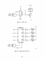
PCR Contents, Pages 20-57, 200-377
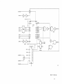
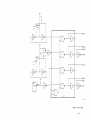
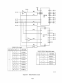
BDVll BLOCK DIAGRAM
Figure 4-1 shows a block diagram of the BDVl1 logic. The DC005 transceivers monitor the LSI-II bus
BDAL lines. When an address in the upper 4K bank of bus addresses is placed on the BDAL lines, the
transceivers gate the address information onto the BDVll DAL lines. If the address is one of those
assigned to the BDVll (173000-173777, 177520, 177522, 177524, 177546), the transceivers generate
ADDRESS MATCH signals. These signals cause the control logic to decode the bus address and to
respond to the protocol signals that effect bus data transfers.
4-4
BHALT L 4
i
I
BREPLYL.4~-----------------------------------------'1
L--~~I
BRPLY
S\lv
Rur~;HAL T
--
RESTART SW
-
BDCOK H
BSYNC L
BWTBT L
BDOUT L
~ I
- DC NOK UH
,
!j;r'
POWER-UP
LOGIC
--
:- ::~Y:~
-----------~:I
-
BDIN L
-
SYNC L/H
A
n
E:
CONTROL
LOGIC
INWD L
REG LlH
.. OUT LB/HB L
-
DAL <0:2> H
--
cl
SYNC L/H
- SEL 0/2/4/6 L
~I
R<0:15> H
BDAL <0: 15> L 4
~ DCOO5
- DAL <0:15> H
TRANSCEIVER rBBS7 L
•
•
ROM
ADDRESS
SELECTION
LOGIC
•
A<10:14> H _
SOCKET
SELECTION
LOGIC
DATA
SELECTOR
I----
I---
r--+
INJO l
SWITCH
REG
I--
READIWRITE
REG
SEt l
I+-
r
SEL4 L
REG L
INWDL
BEVNT L
A<0:10> H
REG L
OUT LB/HB L
XMITH
I
SEL2 L
REG UH
XMITH
OUTLB/HB L
BEVNT
LOGIC
r
SEL6 L
REG L
OUT La L
BEVNT
SW
-0<0:15>
REt H
H
XMIT H
i
SB<1:2> L
SE<1:2> L
ST<l :2>
SP<1:S> L
DAL6 H--.
ROM
SOCKETS
I--
DAL<0:3> H
--.
DISPLAY
LOGIC
-..
DIAGNOSTIC
DISPLAY
01-04
I
SEL4 L
REG L
OUT LB L
MA-1342
Figure 4-1
BDVll Block Diagram
4-5
The bus address placed on the BDAL lines can be the address of one of the BDVII registers, or the
address of a ROM location. If one of the registers has been addressed, the control logic asserts those
signals that are necessary to carry out the operation directed by the protocol signals that follow. For
example, if the 16-bit read/write register is addressed, the control logic asserts the signals that permit
the register to be either read or written. When the actual transfer of data takes place, the information is
gated to or from the register on the DAL lines in response to the protocol signals.
If the bus address is that of a ROM location, the address is loaded into the ROM address selection
logic. This logic includes the PCR, which contains page information previously loaded by a writing
operation into the PCR. The address selection logic decodes the address and asserts relative address
signals (AO H - AIO H) that are applied to all the ROM sockets. Other address signals (AIO H - AI4
H) are applied to the socket selection logic; this logic generates signals that select the particular ROM
identified by the PCR page information. This ROM responds to the relative address signals and places
the data in the addressed location on the 0<0: 15> H lines. The data is then gated onto the DAL lines
by the data selector and placed on the BDAL lines in response to the protocol signals.
The data selector is also used when the PCR is read. When this operation is executed, the peR page
information carried on the R <0: 15> L lines is gated onto the DAL lines and from those lines to the
bus.
All the foregoing logic blocks are described in detail in the following paragraphs. The power-up logic,
the BEVNT logic, and the display logic (all of which are self-descriptive, functionally) are also discussed. For detailed information concerning bus transfer operations, refer to the 1977-1978 Microcomputer Handbook.
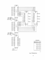
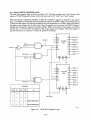
4.3 TRANSCEIVER/SWITCH REGISTER LOGIC
Figure 4-2 shows the transceiver/switch register logic for bits 0-3. The DCOO5 transceiver is a bidirectional buffer between the LSI-II data/address lines, BDAL <0: 15> L, and the BDVII data/address
lines, DAL <0:15> H. The transceiver also provides a constant generator (which is used for selecting
BDVI1 diagnostic and bootstrap addresses) and comparison circuits for address selection.
The transfer of information between the BDAL lines and the DAL lines is controlled by signals XMIT
Hand INWD L, which are generated in the control logic in response to the LSI-II bus protocol
signals. XMIT Hand INWD L are related to bus transfer cycles as follows.
INWD L
XMIT H
Bus Transfer Cycle
LO
LO
HI
HI
LO
HI
LO
HI
No transfer (DAL and BDAL lines open)
DATI (DAL-+BDAL)
}
DATO/DATOB(BDAL-+DAL)
Information can also be put on the BDAL lines by the transceiver JA V inputs. These three inputs drive
three bus lines directly, overriding the XMIT Hand INWD L control signals (JA V3, JA V2, and JA VI
are paired with BUS3, BUS2, and BUSI, respectively, in each DCOO5). A high input causes a low to be
transmitted on the corresponding bus line, while a low or open input causes an open condition to occur
on the bus line. The JAV inputs allow the user to read the contents of the switch register and are
related to the BDAL<0:2> L signals as follows.
BDALIL
BDALOL
JA V3 (HI/LO-OR-OPEN)
JA V2 (HI/LO.-QR-OPEN)
JA VI (HI/LO-OR-OPEN)
*
BDAL2L
(LO/OPEN)*
(LO/OPEN)
(LO/OPEN)
When JA V3, for example, is high, BDALO L is low~ when JA V3 is low or open, BDALO L is open.
4-6
8-{
BDALO L _ _ _ _ _
BDAL1 L _ _ _ _ _9-(
BDAL2 L _ _ _ _1_1-(
BUS3
6
DAT3 ....---DALO H
BUS2
DAT2 7
DAL1 H
DAT1 17
DAL2 H
DATO 18
DAL3 H
BUS1
BDAL3 L _ _ _ _1_2-("
19
DCOOS
+SV----------~JA3
E19
,..-________
2---1 JA2
3
MATCHt----ADDRESS MATCH
t - - - - - - - - - - - - - I JA 1
13
MENB
.--_ _1_6--1 JA V3
.--_1_S-! JA V2
14
JAV1
XMIT
REC
S
4
I
XMiT H
INWD L
E15
3
14
A3
2
1S
A2
16
A1
+SV
REG L
SEL4 L
INWD L
MA-1343
Figure 4-2
Transceiver and Switch Register Logic, Bits 0-3
4-7
The JA inputs of the transceiver are part of the comparison circuits. When the signal state at a JA
input is the same as that at the corresponding bus line, a match exists. If three matches exist, and if the
MENB L signal is low, the MATCH output of the DCOO5 is open-circuited. This open-collector
output permits more than one transceiver output to be wire-ANDed, thereby ~Jrming a somposite
address match signal. The relation between the JA signals and the BDAL signals, and between MENB
L and MATCH H is shown below.
BDALOL
JA3 (GROUND/OPEN)
JA2 (GROUND/OPEN)
JAI (GROUND/OPEN)
BDALIL
BDAL2L
LO/HI
LO/HI
LO/HI
MENBL
J A-BDAL Match
MATCHH
HI
LO
LO
All 3 match
All 3 match
One mismatch
LO
OPEN
LO
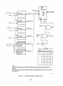
4.4 CONTROL LOGIC
The control logic (Figure 4-3) includes a DCOO4 protocol chip (E8) and an 82S23 PROM (E9). The
PROM monitors LSI-II bus addresses via the DCOO5 transceivers and generates two important signals. One of these, at output DO(I) is asserted (high) when the address of any of the BDVll registers is
placed on the bus. The other, at output Dl(l), is also asserted when a register is addressed; furthermore, this output is wire-ANDed (at A) with two signals from transceiver E17 (MATCH and DAL12
H) to produce an enabling signal when anyone of the assigned bus addresses (173000-173777) is
placed on the BDAL lines.
This enabling signal is applied to the DCOO4 ENB input, allowing this chip to generate signals that
select the BDVl1 registers for data transfers (SELO L, SEL2 L, SEL4 L, and SEL6 L). The DCOO4 also
generates the protocol signals that permit data transfers to take place. Tables 4-5, 4-6, and 4-7 relate
the inputs and outputs of the DCOO4.
As an example of the control logic operation, consider the following description. Figure 4-4 represents
the sequence of operations in a DATO bus cycle. Let us assume that we are going to place page
information in the BDVll PCR, address 177520. When this address is put on the BDAL lines, PROM
E9 asserts outputs DO and Dl, and wire-AND gate A causes the DCOO4 ENB input to go high (because BSYNC L is high, INWD L i~ high and the bus address causes the DCOO5 transceivers to assert
MATCH and DAL signals; refer to Table 4-6). When the processor asserts BSYNC L, flip-flop EI0 is
set, generating the REG H and REG L signals; in addition, the DCOO4 generates SELO L (Table 4-5),
thereby completing the "device-selected" operation in the BDVll (SELO L remains low until BSYNC
L is negated). Now the CPU places the PCR page information on the BDAL lines and asserts BDOUT
L. As Table 4-7 shows, both the OUTHB Land OUTLB L signals, as well as the BRPLY L, signal, are
asserted. (Even though ENB might have gone low when the page information was placed on the
BDAL lines, this input was high when BSYNC L was asserted.)
The OUTHB Land 0 UTLB L signals clock the PCR, loading it with the page information on the
DAL lines. After the CPU negates the BDOUT L signal, the BDVl1 negates BREPLY L and the CPU
terminates the operation by negating BSYNC L.
4-8
J;
E17-MATCH------------------------~t:t:J~-4--------------~
I
DAL12 H - - - - - {
+5V~~--~----~
ENB
~----I
INWD L
VECTOR
DC004
E8
BDAL2 L
BDAL 1 L
DAL2 H------( DAL2
E19
DC005
DAL1 H-----(
DALl
DALO H------I[ ] DALO
BDALO L
SELO L
SEL2 L
XMIT L
SEL4 L
SEL6 L
~
XMIT H
OUT LB L
BWTBT L
BDOUT L-------------------------·
WTBT
DOUT
BDIN L
DIN
OUT HB L
BRPLY L
BSYNC L-----I.
~---''---~----ID
SYNC H
BREPLY L
REG H
L
~--REG
E10
SYNC H
C
DC NOK L
E14-MATCH - - - - . . . . . ,
B
E18-MATCH----~
E19-MATCH------------MA-1344
Figure 4-3
Control Logic
4-9
Table 4-5
DCOO4 Select Outputs
Inputs
Outputs
BSYNCL
END*
DDAL2L* BDALIL* SELOL
SEL2L
SEL4L
SEL6L
L
L
L
L
H
H
H
H
H
H
H
L
H
H
H
H
L
H
H
H
H
L
H
L
H
L
L
L
L
H
H
H
*H and L for these signals indicate the state of the input line at the falling edge of BSYNC.
Table 4-6 DCOO4 Protocol Signals
Inputs
Outputs
BSYNCL
BDINL
ENB*
INWDL
BREPLYL
H
L
X
X
X
H
H
H
L
L
L
L
L
L
L
H
H
H
H
L
*H and L for these signals indicate the state of the input line at the
falling edge of BSYNC.
Table 4-7
DCOO4 Byte Signals
Outputs
Inputs
BSYNCL
BDOUTL ENB*
L
L
L
H
BWTBTL BDALOL* OUTHBL OUTLBL
H
X
L
L
L
L
L
H
L
L
L
BREPLYL
H
L
H
L
H
H
H
X
L
L
L
L
H
H
H
L
L
L
L
*H and L for these signals indicate the state of the input line at the falling edge of BSYNC.
4-10
CPU
BDV11
ADDRESS DEVICE/MEMORY
•
ASSERT BDALO-15 L WITH
ADDRESS AND
•
ASSERT BBS7 L (IF ADDRESS
IS IN THE 28-32K RANGE)
•
ASSERT BWTBT L (WRITE
I"'VI""
1::1
""I""L~I
ASSERT B SYNC L -
-
- - - - - - --"DECODE ADDRESS
•
~
OUTPUT DATA
~
•
REMOVE THE ADDRESS FROM
BDALO-15 L
AND NEGATE BBS7 LAND BWTBT L
(BV'ITBT L REMAINS ACTIVE IF
DATOB CYCLE)
•
PLACE DATA ON BDALO-15 L
•
ASSERT BDOUT L -
...--
~
~
~TAKEDATA
--- -
STORE "DEVICE SELECTED"
OPERATION
•
__ _
_.
RECEIVE DATA FROM BDAL LINES
ASSERT BRPLY L
TERMINATE OUTPUT TRANSFER"'-4"-•
REMOVE DATA FROM BDALO-15 L
AND NEGATE BDOUT L
--- --- -- -- --4-----
- . . OPERATION COMPLETED
____ •
TERMINATE BUS CYCLE
•
TERMINATE BRPLY L
NEGATE BSYNC L (AND BWTBT L
I F A DATOB BUS CYCLE)
MA-1345
Figure 4-4
Operation Sequence, DATa Cycle
4-11
4.5 POWER-UP LOGIC
The power-up logic (Figure 4-5) includes the ENABLE/HALT switch and the RESTART switch. In
normal operation, the ENABLE/HALT switch is in the ENABLE position. When the switch is placed
in the HALT position, inverter E16 causes NAND gate E7A to assert the BHALT L signal. The CPU
enters the halt mode and responds to console ODT commands. To resume operation, the user must
return the switch to the ENABLE position and enter a "P" command at the console terminal.
The REST AR T switch must be cycled to re-boot the system. If the switch is in the position shown in
Figure 4-5, cycling the switch lever generates a pulse that is differentiated by capacitor C13. The
leading edge of the negative spike is inverted by E13 and causes E7B to negate the BDCOK H signal;
thus, DC NOK L is asserted, initializing the BDVII registers. When the negative spike decays, NAND
gate E7B is disabled; the reasserted BDCOK H signal causes the CPU to carry out a power-up sequence and normal operation is resumed. BDCOK H can also be negated by the LSI-II power supply,
which negates the BDCOK H signal if the dc voltages fall below specified levels.
The bus BREPL Y L signal is asserted during the protocol routine when E8 asserts BRPLY. Contrarily, the bus BSYNC L signal causes SYNC H and SYNC L to be asserted, also during the protocol
routine.
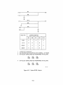
4.6 ROM ADDRESS SELECTION LOGIC
The logic shown in Figure 4-6 decodes the 256 10 LSI-ll bus addresses and produces the 2048 10 addresses needed to access ROM locations. Several examples are given here to illustrate how the logic
works.
In the first example, assume that we want to address location 0400 in the diagnostic/bootstrap ROMS,
which occupy sockets XE53 and XE48. Table 4-1 shows that to address this location we must have
page 2 in the PCR; then, bus address 173000 will access location 0400. It is usual (but not necessary) to
load the PCR with a pair of pages. Therefore, we will put pages 2 and 3 in the PCR by addressing the
PCR at address 177520 and loading it with data 001402; i.e., the PCR low byte contains 002 and the
high byte contains 003 (Figure 4-7).
Now, address 173000 is placed on the LSI-II BDAL lines. Bits 1-8 of the address are loaded into the
flip-flops, E33 (because the bus addresses differ only in the first 9 bits, BDAL<9: 15> L need not be
considered). ROM address bits AO-A6 assume the logic state ofDAL bits 1-7, respectively. The logic
looks at DAL8 H to determine which of the PCR bytes will form ROM address bits A 7-A 14. Since
DAL8 H is low, the low byte is selected; i.e., E32 gates R <0:3> H to A <7: 10> Hand E34 gates
R <4:7> H to A < 11:14> H. Bits AO-AI0 are used to select the ROM location 0400; bits AI1-AI4 are
used to select the correct ROM, i.e., the ROMs in sockets XE53 and XE48. (This procedure is explained in the next section.)
Now that the PCR contains pages 2 and 3, any ROM location from 0400 to 0777 can be addressed.
Consider location 0600, for example, which is addressed by bus address 173400. Example 2 in Figure 47 illustrates the bit selection. Because DAL8 H is high, the high byte of the PCR is selected to form
ROM address bits A7-AI4. Bits AO-AI0 select ROM location 0600, while bits All-AI4 again select
sockets XE53/XE48.
The same bus address, 173400, can address seven other ROM locations, providing the PCR page
number is changed. For example, let us address ROM location 3200. To do this, we must change the
PCR high byte from page 3 to page 15. We can do this either by loading 006414 (pages 14 and 15) into
the PCR or by loading only the high byte with 015. (This can be done by keeping the LSI-ll bus
BWTBT L signal asserted throughout the data transfer cycle; thus, only OUT HB L is asserted and
only the PCR high byte is loaded.) Let us load only the high byte, as illustrated in Example 3, Figure 47. The high byte again forms bits A7-A14 of the ROM address, and we have location 3200 being
addressed.
4-12
+5V
h
..-_~
ENABLE
HALT
r-----------,
I~----------~---------------BHALTL
+5V
I
~----------~---------------BDCOKH
~----------DCNOKH
DC NOK L
B
RESTART
SJ
o
r-----------~--------------BREPLYL
C
r-----------~---------------BSYNCL
+5V
E8
BRPLY L
.-----------SYNCH
SYNC L
D
MA-1346
Figure 4-5
Power-Up Logic
4-13
H~
SH2 OAl 15
74lS273
E27
R8
08
SH2 OAl 14 H----12. 07
R7
SH2 OAl 13 H--.l.i 06
R6
peR
HI
BYTE
SH2 OAl 12 H~ D5
SH2 OAl 11 H~ 04
R5
R4
SH2 OAl 10 H-.2. D3
SH2 OAl 9 H
~ 02
SH2 OAl 8 H
~
R3
R2
R1
01
ClK
11
SH2 REG L
74lS27
SH2 SEL 0 L
~E3
SH2 OUT HB l
~
8
SH3 R15 H
16
SH3R14H
15
SH3R13H
12
SH3 R12 H
9
6
5
2
I
I
I
I
SH3 R10 H
SH3 R9 H
SH3 R8 H
ClR
3
2
2
SH2 DAl 0 H - 2 01
Rl
R2
5
I
R3
6
I
PCR
lO
BYTE
---.!. D4
H .--..!2 05
SH2 DAl 4
R4
R5
SH2 OAl 5 H--l± 06
R6
---22. 07
R7
SH2 OAl 7 H ~ 08
R8
SH2 OAl 6 H
ClK
6
111
SH2 OC NOK L
SH2 OAl 8
SH2 OHl 7
SH2 OAl 6
SH2 OAl4
9
SH3 RO H
SH3 R1 H
SH3 R2 H
SH3 R3 H
B2
~SH3
A2
B1
10
A9 H
~SH3A8
Al
11
6
H
5
3
BO
~SH3A7
AO
2
H
A3
B2
9
F2 ~ SH3A13H
A2
B1
7
F1 ~ SH3 A12 H
Al
BO
4
FO I - - SH3 A 11 H
AO
OUT
CaNT
so
so
~15
11
11
OUT
CaNT
~15
SH3 R6 H
19
SH3 R7 H
~
R7 ~SH3A6 H
R6 ~SH3 A5 H
D6
74lS257 TRUTH TABLE
R5 ~SH3A4 H
---2.i 05
H~ D4
R4 ~SH3 A3 H
-.!.... D3
R3 r-LSH3 A2 H
~ D2
OUTCONT
R2 ~SH3 Al H
Rl
SH2 DAl 1 H---2. D 1
SH2 DC NOK l
r-
12
F3 r - - SH3 A 14 H
B3
SH3 R5 H
07
~11
14
A3
16
H~
H~
SH2 SYNC H
13
'--
ClR
74lS273
E33
ClK
Al0 H
74lS257
E34
SH3 R4 H
19
R8 ~
SH2 DAl 2 H
12
~SH3
15
08
SH2 DAl 3 H
74lS257
E32
12
H~
SH2 OAl 5 H
10
5
SH2 DAl 1 H - . ! 02
SH2 DAl 3 H
14
6
11
SH2 OAl 2 H-..2 03
~ B3
r-
111
SH2 OC NOK L
3
SH2 REG l
74LS27
SH2 SEL 0 l
~E3
SH2 OUT La l
-,
./
SH3 Rll H
11
74lS273
E29
=t2
19
~SH3
AO H
l
CLR
I'
SO
A
B
F
l
L
X
l
l
H
X
H
H
X
l
l
H
X
H
H
MA-1347
Figure 4-6
ROM Address Selection Logic
4-14
6
5
4
3
2
0
0
0
0
0
0
0
0
0
0
0
0
0
DAL <1:8> H
0
0
0
0
O{
A <0:6> H
0
0
0
0
o
0
1514131211109
8
1
0
7
BIT NUMBER
EXAMPLE 1
peR (001402)
0
0
0
0
BDAL L (173000)
0
0
1
0
0
A <7:14> H
0
0
0
0
0
I0
0
1
0
0
0
1
0
0
0
0
0
0
0
0
A <0:10> H (0400)
EXAMPLE 2
peR (001402)
0
0
0
0
0
0
0
0
1
0
BDAL L (173400)
0
1
0
0
0
O.
0
0
0
0
0
0
0
0
0
0
0
a
0
a a
:~O
0
0
0
0
0
0
0
0
0
0
0
0
0
1
0
0
0
0
0
0
0
0
0
01 0
0
0
0
0
0
O{
0
0
0
0
0
o
0
0
0
0
0
0
0
0
DAL <1 :8> H
A <0:6> H
0
A <7:14> H
0
\
0
0
A <0: 10> H (0600)
01
0
0
1
0
0
1
0
1
'"
EXAMPLE 3
peR
1
0
0
0
0
BDAL L (173400)
1
0
DAL <1:8> H
1
I
A <0:6> H
0
A <7:14> H
0
0
0
A <0: 10> H (3200)
0
1
0
'"
MA·1348
Figure 4-7
Address Bit Selection
4-15
Note that the PCR and the flip-flops are cleared whenever DC NOK Lis asseited; this happens when
the REST AR T switch is activated or when the dc voltages drop below reliable operating levels. Also,
since the R <0: 15> H signals can be gated onto the DAL<O: 15> H lines, the PCR can be read as well
as written.
4.7 SOCKET SELECTION LOGIC
The socket selection logic determines which pair of sockets responds to the ROM address signals
(although the ROMs in the sockets actually respond, we will state, for ease of explanation, that the
sockets respond). The selection signals SB1 L, SB2 L, SE1 L, SE2 L, and SP1 L through SP8 L are
generated by two decoders, E30 and E35 (Figure 4-8). Each selection signal causes two sockets to
respond to the address signals; one socket contains the high-byte ROM, the other contains the lowbyte ROM. Table 4-8 includes the relationship between the selection signals and the selected sockets.
Jumpers are inserted selectively in positions W1-W4 and W9-W12. These jumpers cause the PCR page
numbers and the selection signals (and, therefore, the sockets) to be related in definite ways. Earlier,
Table 4-1 indicated that PCR pages are assigned to specific ROM sockets. This is true within the
confines stated for Table 4-1; i.e., the table applies only to the BDV11 module shipped by DIGITAL.
On such a module, jumpers W1-W4 and W9-W12 are arranged as indicated under Group A in Table
4-8. Thus, PCR pages 0-17, for example, cause selection signal SB 1 L to be asserted, and SB 1 L causes
sockets XE53 and XE48 to respond to address signals A<0:10> H. Other combinations of jumpers are
possible, as indicated by Groups B through G in Table 4-8. Note that each selection signal always
selects the same pair of sockets; however, the relation of PCR pages to selected sockets varies with
jumper configuration.
Now, in Example 1 in the preceding section, the PCR was loaded with pages 2 and 3 so that bus
address 173000 could address location 0400. This location was specified by 11 ROM address bits, AO
H - AI0 H. The remaining four ROM address bits, All H - A14 H, are applied to the socket selection
logic; here, they determine the ROMs in which location 0400 is addressed. If we assumme that we have
a BDVI1-AA, which has the Group A jumper arrangement, sockets XE53 and XE48 should be selected; i.e., SB 1 L should be asserted by decoder E30 (Figure 4-8). With a jumper in both W9 and W12,
SBI L is asserted when A14 H is low, A12 H is low, and All H is low (AIO Hand AI3 Hare
irrelevant). Figure 4-7, Example 1, shows that the three signals are low, as they are for all pages in the
0-17 range. That these signals are low for pages 0-17 is indicated by the entry in the primary address
column of Table 4-8; i.e., for addresses in the 0-2K range, address bits All H - A14 H are low. Note
that there is correlation between PCR pages and primary addresses throughout Table 4-8.
The jumper configurations in Groups B-G allow a choice of where program execution begins. That is,
the user can cause the CPU to execute instructions directly from a system ROM or an EPROM when
power is turned on, rather than from the diagnostic/bootstrap ROM. To illustrate, in the preceding
example the PCR contained pages 2 and 3; hence, bus address 173000 addressed location 0400 in
ROMs E53 and E48. However, if jumpers W1-W4 are arranged as shown in Group F, the same PCR
pages, 2 and 3, will cause bus adress 173000 to address location 0400 in ROMs E54 and E49; or, if
jumpers W9-W12 are arranged as in Group B, 173000 will address 0400 in E57 and E40.
Note that in both of these examples, one group of four jumpers is not specified; i.e., W9-W12 are not
specified in Group F and W1-W4 are not specified in Group B. These unspecified jumpers can have
any arrangement as long as there is no conflict in chip selection. To illustrate: If we have the Group F
configuration, we want PCR page 0 to cause 173000 to addresss 0000 in XE54/XE49; but, if jumpers
W9-W12 are arranged as in Group A or B, PCR page 0 causes two other sockets to respond to the
same address. Therefore, either there can be no chips in these other sockets, or the arrangement of
W9-W12 must be changed; for instance, there would be no conflict at all ifW9-W12 were arranged as
in Group C.
4-16
+5V
A14 L
A 14 H
---r-j)or---rl'-----~
W3
o
V'
0
~~~A
yolSP8 L
Y\
Y2
G28
=
=
W4
SP7 L
SP6 L
SP5 L
74S138
E35
SP4 L
A11 H---t~----~~----------------~ A
SP3 L
A12H---r-t--~-+-----------------J 8
SP2 L
W1
A10H---+~-'r-~+-------~
C
SP1 L
W2
o.---J
A13H---+~~r-~+----~o
W12
t--+-----~o
0
I 12B
I
6
2G 2YO'----1
2A
74LS139
E30
L
SE2 L
1I1
.
UIJ~""~
W1~'18
~
I
74S138 TRUTH TABLE
~~~§SE1
2Y3
1Y0t=SB1 L
1Y1
~d _ll_A_~9__
S82L
1Y2
G _ _1_Y...J31
I
IIG-1r-IG-2'-1C-r-IB-'---IA-r--O-UT-LO-W--I
H
!
L
L
L
L
YO (SP8 L)
L
L
H
Y1 (SP7 L)
L
H
L
Y2 (SP6 L)
L
H
H
Y3 (SP5 L)
H
L
L
Y4 (SP4 L)
H
L
H
Y5 (SP3 L)
Il H
H
L
Y6 (SP2 L)
H
H
Y7 (SP1 L)
IH
!
74LS139 TRUTH TA8LE (EACH HALF)
G
L
8
A
L
L
YO(SB1 L)
L
H
Y1 (S82 L)
H
L
Y2 (SE1 L)
H
H
Y3 (SE2 L)
OUT LOW
,
I
l
MA-1349
Figure 4-8
Socket Selection Logic
4-17
Table 4-8
BnVll Selection Signals/Sockets
!
I
IpeR
Group WI W2 W3 W4 W9 WIO WII Wl2 Page
Selection
Signal
Primary
Addresses
(A<O:14>H)
Sockets
Selected
A
R
I
I
R
I
R
R
I
0-17
20-37
40-47
50-57
360-377
340-357
320-337
300-317
260-277
240-257
220-237
200-217
SBI
SB2
SEI
SE2
SPI
SP2
SP3
SP4
SP5
SP6
SP7
SP8
L
L
L
L
L
L
L
L
L
L
L
L
OK-2K
2K-4K
4K-5K
5K-6K
30K-32K
28K-30K
26K-28K
24K-26K
22K-24K
20K-22K
18K-20K
16K-18K
XE53/XE48
XE58/XE44
XE57/XE40
XE52/XE36
XE39/XE50
XE43/XE46
XE47/XE42
XE51/XE38
XE55/XE37
XE60/XE41
XE59/XE45
XE54/XE49
B
*
*
*
*
I
R
I
R
40-57
60-77
0-7
10-17
SBI
SB2
SEI
SE2
L
L
L
L
4K-6K
6K-8K
OK-IK
lK-2K
XE53/XE48
XE58/XE44
XE57/XE40
XE52/XE36
C
*
*
*
*
R
I
R
I
200-217
220-237
240-247
250-257
SBI
SB2
SEI
SE2
L
L
L
L
16K-18K
18K-20K
20K-21K
21K-22K
Ibid
D
*
*
*
*
R
I
I
R
240-257
260-277
200-207
210-217
SBI
SB2
SEI
SE2
L
L
L
L
20K-22K
22K-24K
16K-17K
17K-18K
Ibid
E
I
R
I
R
*
*
*
*
270-277
250-257
230-237
210-217
260-267
240-247
220-227
200-207
SPI
SP2
SP3
SP4
SP5
SP6
SP7
SP8
L
L
L
L
L
L
L
L
23K-24K
21K-22K
19K-20K
17K-18K
22K-23K
20K-21K
18K-19K
16K-17K
XE39/XE50
XE43/XE46
XE47/XE42
XE51/XE48
XE55/XE37
XE60/XE41
XE59/XE45
XE54/XE49
F
R
I
R
I
*
*
Ptr
*
160-177
140-157
120-137
100-117
60-77
40-57
20-37
0-17
SPI
SP2
SP3
SP4
SP5
SP6
SP7
SP8
L
L
L
L
L
L
L
L
14K-16K
12K-14K
10K-12K
8K-I0K
6K-8K
4K-6K
2K-4K
OK-2K
Ibid
*See text describing these configurations.
4-18
Table 4-8
BDVll Selection Signals/Sockets (Cont)
Group WI W2 W3 W4 W9 WI0 WIt W12 Page
G
I
R
R
I
*
*
*
*
I
70-77
50-57
30-37
10-17
60-67
40-47
20-27
n
,...
Selection
Signal
Primary
Addresses
Sockets
,. 0 44> w,,, I Selected
{A< :1
HJ
SP1
SP2
SP3
SP4
SP5
SP6
SP7
L
L
L
L
L
L
L
7K-8K
5K-6K
3K-4K
1K-2K
6K-7K
4K-5K
2K-3K
,...,.....""
T
V-I
""'YT
Ibid
.. T T
V1\..-l1\..
NOTE
R = Removed; I = Inserted
4.8 ROM SOCKETS LOGIC
Figure 4-9 represents the ROM sockets and shows the address signals and enabling signals for each
functional group of sockets. The diagnostic/bootstrap ROM sockets (which are selected by signals
SB 1 Land SB2 L) are supplied with 11 address bits, since these sockets are reserved for 2K-word
ROMs. The EPROM sockets (selected by signals SEI Land SE2 L) are reserved for lK ROMs;
therefore, these sockets are supplied with 10 address bits. The system ROM sockets can be occupied by
either 2K ROMs or 1K ROMs; five jumpers on the BDV11 module permit ROMs of either size to be
used. Figure 4-10 shows how these five jumpers control the selection signals for the system ROM
sockets, and relates the jumpers to the types of ROM that can be used in the BDV11. (If ROMs other
than 8316E, 2716, and 2708 are used, they must meet the specifications given in Appendix A.)
The output data from the selected memory is applied to data selectors that gate the data onto the DAL
< 0: 15> H lines. These selectors also allow the user to read the contents of the peR,
4.9 BEVNT LOGIC
The logic shown in Figure 4-11 permits the user to choose how to control the LTC function. When the
BEVNT switch, E21, is open, the bus BEVNT L signal can be controlled by the LTC signal generated
in the LSI-II power supply. If the switch is closed, the BEVNT L signal can be program controlled.
Program control is effected by the I-bit register, EI0. Address 177546 is placed on the BDAL lines,
causing signals SEL6 L and REG L to be asserted by the control logic. When data bit 6 is issued, the
OUT LB L signal causes E2 to clock the flip-flop, loading it with the state of DAL6 H. If DAL6 H is
high, the flip-flop output turns Q4 off, permitting the LTC signal to assert BEVNT L; but, if DAL6 H
is low, Q4 is switched on and clamps BEVNT L low. Note that the register is cleared when the power is
turned on or when the system is re-booted.
4.10 DISPLAY LOGIC
The display logic and the diagnostic LEDs, DI-D4, are illustrated in Figure 4-12. Address 177524
_.-••, .. ~t.-;
1~"UIl"
: ...
111
!:'.,~ k=:~.. = .-.L..,..-,.1.-=.~
L.£..J
U~1110
,",IV,",l\.,",U
•• ,1.,..,::.~.,. A,,-d- .... k~-!--"
n
'1 '"''''''''' ~",-""""A, -!-1,.,,,,, f'!~= f'!r.= ..... "f.,..,."f'" """"'''<'.::::t. fh.::::t. .,...::::t."''""'.::::t.,.,t~u.::::t.
"11"'11 UCllCl Ull" V-.J
Cl.l,", .l""U,",U,
U.l,", .l.l.lP-.l.lVp VIAl.plAl." "'''IA''''' l.U",
.l"'~l-''''''''l.lY''''
LEDs to glow, indicating the source of the program error. All the flip-flops are cleared when power is
turned on or when the system is re-booted; hence, display value 178 is indicated; i.e., all the LEDs
(including the green POWER OK indicator) are lighted. If the LEDs indicate 178 and the PC =
173000, the ENABLE/HALT switch might be in the HALT position, or a bus error might have
occurred.
4-19
74LS57
DATA
SELECTORS
R <0:15> H
: Bn
(E20)
(E23)
(E28)
(E31 )
A <0:10> H--~-I""XE53/XE48
0 <0:15> H 0 <0:15> H
SB1 L _ _+--1.... 'Hi BYTE/LO BYTE)I-------.,r----""'""-.. An
OUT
CONT
DAL <0:15> H
-
SO
0 <0: 15> H
- - . XE58/XE44
REb H
SB2 L _ _ _-I:... (HI BYTE/LO BYTE)
XMIT H
A <0:9> H---r--.....
Fn
)--
L
0 <0:15> H
XE57/XE40
r---
SE1 L _ _-+---I_~(HI BYTE/LO BYTE)
~ XE52/XE36
0 <0: 15> H
~
REGHXMIT H--:=
SE2 L ---+---1"" (HI BYTE/LO BYTE)
f
~OUT2 L
'---_.-
~
XE39.XE43.XE47
XE51. XE55. XE60 0 <8: 15> H
ST < 1 : 2> ---+---1_" XE59. XE54
SP
< 1:8>
L
SEL2 L---ot>--
- (HI BYTE)
74LS257
I XE50. XE46. XE42 I
lOUT
~.
XE38.XE37.XE41 0 <0:7> H
___""'"".... XE45. XE49
- (LO BYTE)
I
I
CONT
H
L
SO
An
X
I
Bn
Fn
X
X
HI-Z
L
L
X
L
L
H
X
H
H
X
L
L
H
X
H
H
NOTE:
XE53/X48. XE58/XE44 ARE DIAGNOSTIC ROM SOCKETS (XE58/XE44 RESERVED FOR
DIGITAL);
XE57/XE40. XE52/XE36 ARE EPROM SOCKETS; REMAINING SOCKETS ARE 16K SYSTEM
ROM SOCKETS.
MA-1350
Figure 4-9
Logic Block Diagram, ROM Sockets
4-20
W7
A10 H
o
+12 V
o
ST2
0
W8
I
r
+Sv
0
W13
ST1
~~
J
I
1
W6
CB2
o
0
r
DB2
ROM TYPE
JUMPERS INSERTED'
WS
W6
W7
W8
W13
2708 2
R
I
R
I
R
2716
R
R
I
R
I
8316E3
I
R
I
R
R
8316E4
R
R
I
R
I
1.
!=!!\JSERTED; R=REMOVED
2.
3.
CB2 AND DB2 MUST BE SUPPLIED WITH EXTERNAL -SV POWER.
CHIP SELECT SIGNALS MUST BE PROGRAMMED AS FOLLOWS:
CS1
LOW
4.
CS2
LOW
CS3
LOW
CHIP SELECT SIGNALS MUST BE PROGRAMMED AS FOLLOWS:
CS1
LOW
CS2
LOW
CS3
HIGH
MA·1351
Figure 4-10
System ROM Jumpers
4-21
+5V
+5V
DAL6 H
REG L
OUT LB L
SEL6 L
0
t----IC
DC NOK L
MA-1352
Figure 4-11
BEVNT Logic
+5V
74LS175
E25
R3(1)
DAL3 H ----103
R3(0)
DAL2 H----tD2
R2(1)
R2(0)
R 1 (1)
R1 (0)
D2
DAL1 H----tD1
RO(1)
RO(O)
01
DALO H----tDO
CLK
CLR
REG L
OUT LB L
SEL4 L
DC NOK L - - MA-1353
Figure 4-12
Display Logic/LEDs DI-D4
4-22
4.11 READ/WRITE REGISTER LOGIC
The read/write register logic is shown in Figure 4-13. The logic includes two 8-bit universal shift
registers, 74LS299 integrated circuits, which are used only in the "hold" and "load" modes.
When the register is addressed, the SEL2 L, REG H, and REG L signals are asserted by the control
iogic. If the register is being read, the control logic also asserts the XMIT H signal. The asserted OUT2
L signal puts the register into the hold condition; thus, the information on the DAL lines is that held in
the register output stages. On the other hand, when the register is to be written, the XMIT H signal is
negated and the register is placed in the load condition. Either or both bytes of the register are clocked
and the data on the DAL lines is loaded into the output stages of the register. The entire register is
cleared when power is turned on or when the system is re-booted.
S/l
SIR
OUT2 l
74lS299
E22
~
rfl
'\
,
)
DAL14 H
R5
DAl9 H
DII
S1
"..,.
DAL13 H
ClK
R3
DAL1 0 H
R2
pAL 12 H
R1
DAl11 H
SO
SEl2 l
REG l
DAl8 H
OH'
OA'
REG H
XMIT H
OUTHB l
DAl15 H
I
ClR
~
G1
G2
Y
S/l
SIR
OH'
OA'
DAl7 H
74lS299
E24
SO
S1
ClK
OUTlB l
74lS299
ClR
ClR
S1
SO
ClK
Rn
l
X
l
X
l
l
l
X
X
l
H
l
l
X
H
H
H
i
G1
DAlO H
DAl6 H
R5~DALI
H
R4
DAl5 H
R3
DAl2 H
R2
DAl4 H
R1
DAl3 H
G2
DC NOK l
HOLD CONDITION
I
LOAD CONDITION
I
MA-1354
Figure 4-13
Read/Write Register Logic
4-23
APPENDIX A
ROM SPECIFICATIONS
This appendix gives specifications of the ROMs recommended for use in BDVII variations. If ROMs
other than those listed are used, they must meet the specifications listed here.
A-I
2708-TYPE EPROM (IK X 8 ORGANIZATION)
READ OPERATION
DC AND OPERATING CHARACTERISTICS
=
=
TA
0° C TO 70° C, VCC
+5 V ±5%, VOO
UNLESS OTHERWISE NOTED.
SYMBOL
PARAMETER
MIN.
AC CHARACTERISTICS
MAX.
UNIT
= 5.25V or Y,N = V,L
10
ILO
OUTPUT LEAKAGE
CURRENT
10
IOD[3]
VDD SUPPLY
CURRENT
65
Iccl 3 J
VCC SUPPLY
CURRENT
10
rnA
ALL INPUTS HIGH
ISS[3J
VSS SUPPLY
CURRENT
45
rnA
CSIWE
..
....
-.
INPu I LOW
_-
'"
J.l.A
=
TA
0° eTO 70° C. VCC
+5V ±5%, VOD
UNLESS OTHERWISE NOTED.
Y,N
= 5.5 V, CSIWE = 5 V
J.l.A
VOUT
rnA
WORST CASE SUPPLY CURRENTS:
= 5V;
TA
I
= 0°
= +12 V ±5%, VBS = -5 V ±5% VSS = OV.
2708-1 LIMITS
MIN.
MAX.
CONDITIONS
ADDRESS AND CHIP
SELECT INPUT
SINK CURRENT
III
=
= +12 V ±5%, VBB[l] = -5 V ±5%, VSS = 0 V,
SYMBOL
PARAMETER
tACC
ADDRESS TO OUTPUT
DELAY
tco
CHIP SELECT TO
OUTPUT DELAY
tDF
CHIP DESELECT TO
OUTPUT FLOAT
0
tOH
ADDRESS TO OUTPUT
HOLD
0
2708 LIMITS
MIN
MAX.
UNITS
350
450
ns
120
120
ns
120
ns
120
0
ns
0
C
CAPACITANCE[1 ]
.
.
TA = 25° C, f = 1 MHz
VOLTAGE
iNPUT HIGH
VOLTAGE
I V,H
VOL
OUTPUT LOW
VOLTAGE
VOHl
OUTPUT HIGH
VOLTAGE
VOH2
OUTPUT HIGH
VOLTAGE
POWER
DISSI PATION
PD
NOTES:
1.
2.
3.
13.0
SYMBOL
PARAMETER
TYP.
MAX. UNIT CONDITIONS
C'N
INPUT CAPACITANCE
4
6
pF
Y,N
OUTPUT CAPACITANCE S
12
pF
VOUT
Vce+11 V
0.45
'3.7
V
V
2.4
V
SOO
rnW
10L
10H
10H
TA
= 1.6 rnA
= -100 J.l.A
= -1
= 70°
COUT
1.
PIN CONFIGURATION
THIS PARAMETER IS PERIODICALLY SAMPLED AND IS NOT
100% TESTED.
V
24Lvcc
I
=
OUTPUT LOAD: 1 TTL GATE AND CL
100 pF
INPUT RISE AND FALL TIMES: ~20 ns
TIMING MEASUREMENT REFERENCE LEVELS: O.S V AND
2.8 V FOR INPUTS; O.S V and 2.4 V FOR OUTPUTS.
INPUT PULSE LEVELS: 0.65 V TO 3.0 V
PIN NAMES
AO-AS
ADDRESS INPUTS
01- 0 S
DATA OUTPUTS/INPUTS
-
__
r~
... _
.
-- ..... -_ .. _ - - . - ...
Il,;HIP SELECT/WRITE ENABLE INPUT I
I
I
...."._.
23
AS
AS!1]
A5
VSB MUST BE APPLIED PRIOR TO Vee AND VOO. VaB MUST ALSO BE THE LAST
POWER SUPPLY SWITCHED OFF.
THE TOTAL POWER DISSIPATION OF THE 2704/270S IS SPECIFIED AT SOO rnW, IT IS
NOT CALCULATED BY SUMMING THE VARIOUS CURRENTS ODD, ICC, and 'BB)
MULTIPLIED BY THEIR RESPECTIVE VOLTAGES SINCE CURRENT PATHS EXIST
BETWEEN THE VARIOUS POWER SUPPLIES AND VSS. THE IDD, ICC, AND IBB
CURRE~~TS SHOULD BE USED TO DETERiviiNE PO'vVER SUPPLY CAPACiTy Oi~LY.
~ ....t
1"'\/
A6
AC TEST CONDITIONS:
TYPICAL VALUES ARE FOR TA = 25° C AND NOMINAL SUPPLY VOLTAGES.
= OV
NOTE
rnA
C
= OV
A4
4
VBB
A3
5
CSIWE
A2
6
270S/2704
\
Al
VDD
PROGRAM
(LSB) AO
07 (MSB)
(LSS) 00
06
01
05
02
04
VSS
03
-'
NOTE 1: PIN 22 MUST BE CONNECTED
TO VSSFOR THE 2704.
MA·1381
A-3
8316E-TYPE ROM (2K X 8 ORGANIZATION)
AC CHARACTERISTICS
DC AND OPERATING CHARACTERISTICS
TA
I
I
= 0°
C TO +70° C,VCC
= 5 V ±10%
TA
UNLESS OTHERWISE SPECIFIED.
i
LIMITS
MIN. MAX.
= 0°
C TO +70° C, VCC
= +5 V ±10%, UNLESS OTHERWISE
I
UNIT
TEST CONDITIONS
f..tA
VIN
SPECIFIED.
LIMITS
MIN.
MAX.
SYMBOL
PARAMETER
tA
ADDRESS TO OUTPUT DELAY TIME
450
ns
tco
CHIP SELECTTO OUTPUT ENABLE DELAY TIME
120
ns
tDF
CHIP DESELECTTO OUTPUT DATA
FLOAT DELAY TIME
100
ns
UNIT
SYMBOL
PARAMETER
III
INPUT LOAD
CURRENT
(ALL INPUT PINS)
10
OUTPUT LEAKAGE
CURRENT
10
ILOL
OUTPUT LEAKAGE
CURRENT
-20
f..tA
CHIP DESELECTED, VOUT =
0.4 V
CONDITIONS OF TEST FOR
AC CHARACTERISTICS
ICC
POWER SUPPLY
CURRENT
120
rnA
ALL INPUTS 5.25 V DATA OUT
OPEN
VIL
INPUT "LOW"
VOLTAGE
O.S
V
OUTPUT LOAD ............................................................................................... 1 TTL GATE AN D CL = 100 pF
!N PUT PU LSE LEVELS ...................................................................................................................0.8 TO 2.4 V
INPUT PULSE RISE AND FALL TIMES (10% TO 90%) .........................................................................20 ns
TIMING MEASUREMENT REFERENCE LEVEL
INPUT ........................................................................................................................................ 1 V AND 2.2 V
OUTPUT ................................................................................................................................O.S V AND 2.0 V
VIH
INPUT "HIGH"
VOLTAGE
ILOH
-0.5
2.4
VOH
OUTPUT "HIGH"
VOLTAGE
0.4
2.4
5.25 V
CHIP DESELECTED, VOUT
4.0 V
=
II
I
I
I
I
V
V
V
CAPACITANCE[21
IOL
IOH
= 2.1
PIN CONFIGURATION
TA = 25° C. f = 1 MHz
rnA
= -400 f..tA
SYMBOL
TEST
CIN
ALL PINS EXCEPT PIN UNDER
TEST TIED TO AC GROUND
COUT
ALL PINS EXCEPT PIN UNDER
TEST TIED TO AC GROUND
NOTE
1.
10
VCC
+1.0 V
OUTPUT" LOW"
VOLTAGE
VOL
f..tA
= 0 to
TYPICAL VALUES FOR TA = 25° C AND NOMINAL SUPPLY VOLTAGE.
NOTE
2.
LIMITS
TYP.
MAX.
5 pF
.
1 ('\
....,
n~
...,-
A7
2
A5
3
A9
4
CS3
A3
5
CS1
A10
10 pF
1
c:
I V
VCC
A6
AS
_I:
tJl
THIS PARAMETER IS PERIODICALLY SAMPLED AND IS
NOT 100% TESTED.
A2
6
A1
7
CS2
AO
S
D7
DO
9
06
01
10
02
11
04
GND
12
D3
15
D5
PIN NAMES
AO-A10
ADDRESS INPUTS
07- 0 0
DATA OUTPUTS
I CS1-CS3 ICHIP SELECT INPUTS I
MA·1382
A-5
2716-TYPE EPROM (2K X 8 ORGANIZATION)
PIN CONFIGURATION
READ OPERATION
DC AND OPERATING CHARACTERISTICS
TA
= 0°
C To 70° C, VCcl1.2]
SYMBOL
PARAMETER
III
INPUT LOAD
CURRENT
ILO
IPP11 2 ]
ICC1[2]
ICC2[2]
I VIH
±5%, Vpp [2]
LIMITS
MIN. MAX.
10
OUTPUT LEAKAGE
CURRENT
10
Vpp CURRENT
5
= Vee
TA = 0° C TO 70° C, vccl 1 ] == +5 V ±5%, vpp[2] == Vec ±0.6 V [3]
±O.6 V[3]
UNIT
CONDITIONS
/lA
VIN
/lA
= 5.25 V
VOUT
•• I ·
= 5.25 V
SYMBOL
PARAMETER
tACC1
ADDRESS TO
OUTPUT DELAY
LIMITS
MIN. MAX.
450
PD/PGM TO OUTPUT
tACC2
UNIT
TEST CONDITIONS
ns
PD/PGM
-
ns
450
- = VIL
= CS
= VIL
CS
DELAY
VCC CURRENT
(STANDBY)
25
VCC CURRENT
(ACTIVE)
100
INPUT LOW
VOLTAGE
VIL
= +5 V
A~~1
AC CHARACTERISTICS
-0.1
0.8
rnA
mA
rnA
Vpp
= 5.85 V
PD/PGM
CS
= VI H,
CHIP SELECT TO
OUTPUT DELAY
tco
CS
= VI L
ns
120
= VIL
tPF
PD/PGM TO OUTPUT
FLOAT
0
100
ns
CS
tDF
CHIP DESELECT TO
OUTPUT FLOAT
0
100
ns
PD/PGM
= PD/PGM = VIL
= VIL
PD/PGM
INPUT HIGH
VOLTAGE
I
ADDRESS TO
OUTPUT HOLD
ns
PO/PGM
?L1h
Vr'r'
---... .....
~v
A6
2
Aa
A5
3
AS
A4
4
VPP
A3
5
CS
A2
6
A10
A1
7
PD/PGM
AO
8
07
00
9
06
0,
10
05
02
11
04
GND
12
03
PIN NAMES
AO-A10
0
V
~
= VIL
V
. tOH
•
-
= CS = V! L
ADDRESSES
PD/PGM POWER DOWN/PROGRAM
CS
CHIP SELECT
00-07
OUTPUTS
CAPACITANCE[4]
VOL
OUTPUT LOW
VOLTAGE
VOH
OUTPUT HIGH
VOLTAGE.
0.45
2.4
= 2.1
V
10L
V
10H = -400/lA
rnA
NOTES
TA = 25° C, f = 1 MHz
SYMBOL
PARAMETER
CIN
INPUT CAPACITANCE
4
6
Cf"iIIT
nllTPllT CAPACITANCE
8
12
VUI
1.
VCC MUST BE APPLIED SIMULTANEOUSLY OR BEFORE VPP AND REMOVED
SIMULTANEOUSLY OR AFTER Vpp.
2.
VPP MAY BE CONNECTED DIRECTLY TO VCC EXCEPT DURING PROGRAMMING. THE
SUPPLY CURRENT WOULD THEN BE THE SUM OF ICC AND IPP1.
AC TEST CONDITIONS
TYP. MAX.
UNIT
CONDITIONS
pF
VIN
nF
/"
I
= OV
Vf"iIIT
VVI
=
OV
OUTPUT LOAD:1 TIL GATE AND CL = 100 pF
INPUT RISE AND FALL TIMES:
~20 ns
INPUT PULSE LEVELS:
0.8 V TO 2.2 V
T!MING MEASUREMENT REFERENCE LEVEL:
INPUTS
1 V AND 2 V
OUTPUTS
0.8 V AN 0 2 V.
MODE SELECTION
3.
THE TOLERANCE OF 0.6 V ALLOWS THE USE OF A DRIVER CIRCUIT FOR SWITCHING
THE VPP SUPPLY PIN FROM VCC IN READ TO 25 V FOR PROGRAMMING.
~s
MODE
PD/PGM
(18)
CS
(20)
Vpp
(21 )
VCC
(24)
OUTPUT
(S-11 , 13-1 7)
READ
VIL
VIL
+5
+5
DOUT
4.
THIS PARAMETER IS ONLY SAMPLED AND IS NOT 100% TESTED.
DESELECT
DON'T CARE
VIH
+5
+5
HIGH Z
5.
tACC2 IS REFERENCED TO PD/PGM OR THE ADDRESSES, WHICHEVER OCCURS
LAST.
POWER DOWN
VIH
DON'T CARE +5
+5
HIGH Z
PROGRAM
PULSED
VIL TOVIH
VIH
+25
+5
DIN
I 11U\.:ii'lMivi vi:nill
\ Iii
vlL
\. J:;
vlL~
I. ..L'l£:
I 'OJ
-L.!:
n ........... _
'"'UUI
PROGRAM INHIBIT
VIL
VIH
1+ 25
+5
HIGH Z
CO"""''"'''" ••
"r-r""tlr-V
.
.w
MA-1383
A-7
Reader's Comments
BDVll BUS TERMINATOR,
BOOTSTRAP, AND DIAGNOSTIC ROM
TECHNICAL MANUAL
EK-BDVII-TM-OOI
Your comments and suggestions will help us in our continuous effort to improve the quality and usefulness of our
publications.
What is your general reaction to this manual? In your judgment is it complete, accurate, well organized, well
written, etc.? Is it easy to use? ~~~~~~~~~~~~~~~~~~~~~~~~~~~~~
What features are most useful? _~~_~~~~~~~_~~~~~~_~~~~~~_~~~
What faults or errors have you found in the manual?
~~~~~~~~~~~~~~~~~_~_
Does this manual satisfy the need you think it was intended to satisfy?
Does it satisfy your needs? _ _ _ _ _ _ _ _ _ _ _ __
D
~_~_ _~_ _~~_ __
Why? _______________________
Please send me the current copy of the Technical Documentation Catalog, which contains information on
the remainder of DIGITAL's technical documentation.
Name
~
_ _ _ _ _ _ _~~~~~_ __
Street ~~~~~~~~_~~~~~~_ __
City ~_ _ _ _ _ _ _ _ _ _ _ _ _ _ _ _ __
Title ~_ _ _ _~~_ _~~~~_ _~_
Company _ _ _~_ _ _ _ _ _ _ _ _ _ _~ State/Country
Department ~_______________ Zip
Additional copies of this document are available from:
.......... -. 1.......·
,...,.,
.i.Jlgnai
eqUipment. corporation
444 Whitney Street
Northboro, Ma 01532
Attention: Communications Services (NR2/MI5)
Customer Services Section
Order No. ______E_K_-_B_D_V_I_I_-T_M
__
-O_O_I_______
~
________________
-----------~~-----------
-
-
-
-
-
-
-
-
DoNotTear-FoldHereandStaple
-
-
-
-
-
-
--
FIRST CLASS
PERMIT NO. 33
MA YNARD, MASS.
BUSINESS REPLY MAIL
NO POSTAGE STAMP NECESSARY IF MAILED IN THE UNITED STATES
Postage will be paid by:
Digital Equipment Corporation
Technical Documentation Department
Maynard, Massachusetts 01754
digital equipment corporation
Printed in U.S.A.