1
UNCLASSIFIED______________
S E C U R I T Y C L A S S I F I C A T I O N O F T H I S P A G E (When D a t a E n te re d )
READ INSTRUCTIONS
B EFO R E COMPLETING FORM
REPORT DOCUMENTATION PAGE
3.
R E C IP IE N T ’ S C ATA LO G NUMBER
T I T L E (a n d Su bti tle)
5.
T Y P E OF R E P O R T & P E R IO D C O V E R E D
A SIGNAL AVERAGER INTERFACE BETWEEN A
BIOMATION 6 500 TRANSIENT RECORDER AND
A LSI-11 MICROCOMPUTER
6.
P E R F O R M I N G O R G. R E P O R T N U M B E R
A U T H O R fs .)
8.
C O N T R A C T OR G R A N T N U M B E R fsJ
d.
REPOR T NUMBER
4.
7.
2. G O V T A C C E S S I O N NO.
Technical Report
L. T. Specht
9.
N00014-79-C-0424
10.
P E R F O R M IN G O R G A N IZ A T IO N N AM E AN D ADDRESS
PROGRAM ELEM ENT, P R O JE C T, TASK
A R E A & WORK U N I T N U M B E R S
Coordinated Science Laboratory
University of Illinois at Urbana-Champaig n
Urbana, IL 61801
11.
12.
C O N T R O L L IN G O F F IC E NAME AND ADDRESS
REPORT DATE
June 1980
Joint Services Electronics Program
13.
NUMBER OF PAGES
55
14.
M O N IT O R IN G AG EN C Y N AM E
a
A D D R E S S ( i t different from C o n t r o l l i n g O f f i c e )
15.
S E C U R I T Y C L A S S , (o f this report)
UNCLASSIFIED
15a.
16.
D E C L A S S I FI C A T I O N / D O W N G R A D I N G
SCHEDULE
D I S T R I B U T I O N S T A T E M E N T ( o f this R e po rt )
Approved for public release; distribution unlimited.
17.
D I S T R I B U T I O N S T A T E M E N T ( o f the abstract entered in B l o c k 20, i f different from R epo rt)
\
18.
S U P P LE M E N T A R Y NOTES
19.
K E Y WORDS (C o n t i n u e on reverse side if n e c e s s a r y and id e n ti fy by bl o ck number)
Signal averager
Transient recorder
Computer Interfacing
20.
A B S T R A C T ( C o n t i n u e on reverse side if n e c e s s a r y and id e n ti fy by bl o c k number)
This report describes the design and implementation of a
versatile and compact signal averager interface between a
Biomation 6 50 0 transient recorder and a LSI-11 microcomputer.
The design allows for fast signal averaging in excess of 1 kHz
and is also easily software configurable and controllable. The
interface has been incorporated into an LSI-11 system using the
RT-11 operating system and found to perform very satisfactorily.
DD
i
J n 73 1473
ih/j
E D I T I O N O F 1 N O V 65 IS O B S O L E T E
UNCLASSIFIED
S E C U R I T Y C L A S S I F I C A T I O N O F T H I S P A G E (When D a ta E n te re d )
i
S E C U R I T Y C L A S S I F I C A T I O N O F T H I S P A Q E f W i o n Data Bntarad)
S E C U R I T Y C L A S S I F I C A T I O N O F T H I S P A G E f W i e n D a ta E n te r e d )
A SIGNAL AVERAGER INTERFACE BETWEEN A BIOMATION 6500
TRANSIENT RECORDER AND A LSI-11 MICROCOMPUTER
by
L. T. Specht
This work was supported in part by the Joint Services
Electronics Program (U. S. Army, U. S. Navy and U. S. Air
Force) under Contract N00014-79-C-0424.
Reproduction in whole or in part is permitted for any
purpose of the United States Government.
Approved for public release.
Distribution unlimited.
A SIGNAL AVERAGER INTERFACE BETWEEN A BIOMATION 6500
TRANSIENT RECORDER AND A LSI-11 MICROCOMPUTER
L. T. Specht
Department of Electrical Engineering and
Coordinated Science Laboratory
Abstract
This report describes the design and implementation of a
versatile and compact signal averager interface between a
Biomation
6
50 0 transient recorder and a LSI-11 microcomputer.
The design allows for fast signal averaging in excess of 1
kHz and is also easily software configurable and controllable.
The interface has been incorporated into an LSI-11 system
using the RT-11 V3B operating system and found to perform
very satisfactorily.
1
1.
INTRODUCTION
This is the description of a versatile signal averaging
system based around a Digital Equipment Corporation (DEC) LSI11 microcomputer and a Biomation
6
50 0 transient recorder (TR).
With the widespread utilization of LSI-11’s in various experi
mental configurations, it is convenient to have a signal averager
(SA) plug-in that would interface a transient recorder front end
unit with the computing power of an LSI-11.
This would elimin
ate, in many cases, the need for an external signal averager
mainframe in order to incorporate a TR into an existing LSI-11
based system.
Besides providing a rather large cost savings,
this results in a more compact system that is both versatile
and easy to use.
The SA interface described herein is com
patible with either the DEC LSI-11, LSI-11/2 or LSI-11/23 CPU
and any system based on one of these CPU's and which will hence
forth be referred to as simply LSI-11.
At this point a brief description of what is meant by a
signal averager and transient recorder may be in order.
Basi
cally, a signal averager adds together waveforms that are
synchronized in time so that any coherent features that are
present will add constructively; whereas, any incoherent features
will add destructively.
In this way the ratio of signal to noise
(SNR), or coherent to incoherent features, can be increased
from that which it is for any given waveform.
Typically the
2
addition is done digitally which necessitates the need to be
able to digitally represent the original analog signal.
This
is done by digitizing the analog signal at N time intervals of
At each with an analog-to-digital converter (ADC) so that the
total time sampled is NAt.
Thus for each sampled point the
time resolution is defined by At and the amplitude resolution
is determined from the number of bits in the ADC.
For fast
signals the sampling interval At is usually too short for any
type of real time processing so that some form of buffer memory
is used to temporarily store the digitized waveform before it
can be processed.
This combination of ADC, sampling clock, and
buffer memory is referred to as a transient recorder.
Biomation
6
For the
500 transient recorder the main specifications are:
(1) minimum sampling interval of 2 ns, (2) total of 10 24
sampled points, (3) ADC resolution of
6
bits, and (4) maximum
output rate for the stored waveform (1024 words of
of 500 ns/word.
6
bits each)
As an aside, one should note that the above
restriction of non real time signal processing of fast signals
can be eliminated by incorporating a transient recorder and
signal averager into one integral unit.^
The main impetus
for real time processing is to obtain the maximum repetition
rate possible since the SNR improves as the square root of the
number of waveforms averaged.
In typical experimental configurations some form of addi
tional data manipulation is usually required after the averaged
3
waveform has been obtained.
This may include addition and
subtraction of waveforms to remove undesirable coherent
features, integration, differentiation, Fourier transform,
graphical display, handcopy output, waveform storage, etc.
When used in conjunction with an LSI-11 system all of these
features and more .are readily programmable and changeable as
the user's needs change.
Also since the SA interface is soft
ware controllable it is readily amenable to incorporation into
an automated environment.
In view of the above considerations the main features that
the SA interface incorporates are as follows.
1)
Plug-in capability - everything is contained on a single
quad size printed circuit board.
2)
High data taking rate - this allows for a 1-1.5 kHz
repetition rate for transferring a 1024 point acquired wave
form.
3)
Low CPU dead time - at the maximum repetition rate
there is only approximately
4)
2
% dead time for any length of time.
No premanipulation of stored data - the signal averaged
waveform is stored in either single precision (16 bit) or
double precision (32 bit) integer format.
5)
x-y analog outputs - two 10 bit DAC CRT monitor outputs
are provided for either real time viewing of the signal aver
aged waveform or programmed display of the memory contents.
4
6
)
Software controllable and configurable - see the soft
ware section for the various options and configurations that
may be implemented by the CSR.
7)
Ease of operation and extensive data manipulation -
this is basically a characteristic of the LSI-11 system and
corresponding software.
As a final note, while the SA interface described here is
specifically for use with the 6500 any other TR that uses a
similar means of data transmission can be utilized as a front
end unit.
Namely, the 6500 uses a word-serial, bit-parallel
data transfer under a "handshake" control.
See the circuit
I
description for more information if the SA interface is to be
used with another TR.
5
2-.
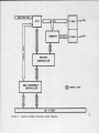
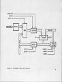
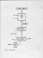
HARDWARE OVERVIEW
The basic block diagram of the SA interface is illustrated
in Figures 1-5.
There are five major functional sections:
1)
arithmetic logic unit (ALU), 2) memory, 3) x-y DAC, 4) DMA/
interrupt controller, and 5) master controller.
Each of these
five sections will now be briefly described, a more complete
discussion can be found in the circuit description section.
The ALU section is basically a 16-bit adder whose B input
is the memory data bus (MEM 0-15) and whose A input can be
either the
6
(DATA 0-15).
500 data bus (PERDATA 0-5) or the SA data bus
Both the A and B inputs can be set to zero via
the data output register (DATOR) and the sum latch, respectively.
The adder output is written into the sum latch which can be
placed back on the memory data bus, and the data input regis
ter (DATIR) which can be placed back on the SA data bus.
allows the ALU to operate on the
bus in one of three ways:
1
6
This
500 data bus or the SA data
) add to memory,
2
) overwrite
memory, or 3) write zero to memory.
The memory consists of four lkx4 bit static RAMs arranged
as lkxl6 bit words.
The memory address (MA) is generated by
the memory address counter and stored in the memory address
register.
For display purposes the MA counter may also be
continuously clocked at a 1 MHz rate.
6
A x-y CRT monitor output is available through two 10-bit
DACs.
The x-DAC monitors the memory address bus; whereas, the
y-DAC monitors the 9 least significant bits and the most signi
ficant sign bit of the memory data bus, assuming that data is
stored as signed z's complement fixed point numbers.
channel provides a ±5V full scale output.
Each
A 12V inverter is
provided for the DACs so that the only backplane voltages re
quired are +5V and +12V.
A z-blank output is also available.
The x-y output can be used to monitor the memory contents either
real time during signal averaging, or under program control.
The DMA/interrupt control section is capable of performing
DATI, DATIB, DATO, and DATIO bus cycles which are input, output,
and input/output (read-modify-write) transfers between the
LSI-11 and the SA interface.
This section contains the LSI-11
bus transceivers and logic to implement interrupt requests,
address control, protocol, and DMA requests.
in this section are five registers:
1
Also contained
) word count register
(WCR), 2) bus address register (BAR), 3) control status regis
ter (CSR), 4) data input register (DATIR), and 5) data output
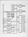
register (DATOR). The device address and interrupt vector
are switch selectable as illustrated in Figure
6
thus establish
ing the five register addresses and the two interrupt vectors.
A brief functional description of each of the five registers
is given below.
7
1)
The WCR is used to control the number of words trans
ferred during a DMA cycle.
It is loaded with the 2's complement
of the number of words to be transferred and is incremented
after each word is transferred.
The DMA cycle is terminated
when the word count reaches zero.
2)
The BAR provides the memory address to or from which
data is to be transferred.
It is loaded with the starting
address of the transfer and is incremented after each word
is transferred.
3)
The DATIR and DATOR are write only and read only
registers sharing the same register address.
These registers,
as the others, can be accessed under program control but are
typically used during a DMA cycle to buffer data into or out
of the SA interface.
4)
The CSR is used to control the functions and monitor
the status of the SA interface.
The SA interface may be con
figured in many different ways through the use of the CSR; refer
to the software section for a description of each of the CSR
bit functions.
The master control section provides the control structure
for interconnecting the other sections of the SA interface.
This includes handling communication with the
6
500, keeping
track of the number of processed waveforms, initiating DMA re
quests, and implementing the various configurations setup through
the CSR.
8
Typical cycle times are 700-900 ns per word, which for the
1024 word waveform stored in the
tion rate of 1-1.5 kHz.
6
500 allows a maximum repeti
At this rate a SNR improvement of 10 0
can be obtained in 10 seconds.
Also at the maximum rate a DMA
cycle is requested every .5 seconds which takes approximately
8
ms for a double precision transfer thus giving rise to ap
proximately 2% CPU dead time.
9
3.
SOFTWARE
This section discusses the SA interface from a software
point of view with the intention that the reader may learn how
to use the SA interface without having to become familiar with
all of the hardware.
It is assumed that the reader is somewhat
familiar with the LSI-11 software, if not, one can consult the
'LSI-11 Microcomputer Handbook".
2
The SA interface is programmed through the five registers
contained in the DMA/interrupt section:
and DATOR.
WCR, BAR, CSR, DATIR,
Each of these registers has a unique address
established by the device address, and as such each is acces
sible under program control.
The WCR and BAR are used during
DMA cycles to keep tract of the number of words transferred and
to provide a memory address to or from which each word is trans
ferred.
The WCR is loaded under program control with the 2 ’s
complement of the number of words to be transferred and the
BAR is loaded with the starting address.
The DATIR and DATOR
can also be accessed under program control to read or write in
formation out of or into the SA memory.
Each time either the
DATIR or DATOR is accessed the memory address is advanced to
the next location.
Normally the DATOR and DATIR are used
during DMA cycles to buffer data into or out of the SA inter
face.
The CSR is used to control and monitor the status of
the SA interface.
A brief description of each of the 16 CSR
10
bit functions is given in Table 1.
written under program control.
Each bit can be read or
Bits 4 and 5 of the CSR are
special in that they are the extended memory address bits XAD
16 and 17 making the SA interface compatible with the memory
management unit (MMU) of the LSI-11/23.
Two interrupt vectors are also selectable on the SA inter
face.
They are typically used by interrupt requests generated
at the end of a DMA cycle or due to an error condition to point
to interrupt service routines.
A very simple program illustra
ting the use of these registers and the interrupt vectors in
normal operation is provided in Figure 7.
Data can be transferred during a DATIO cycle in either
single or double precision format.
results in a.16 bit signed
2
Single precision format
's complement fixed point integer
(INTEGER*2); whereas, double precision format results in a 32
bit result (INTEGER*4).
Since the data is placed in standard
integer format no premanipulation of the data is necessary.
The double precision format also allows very extensive signal
averaging for long lengths of time without loss of precision.
Besides the normal DATO or DATIO cycle transfers, data may
also be transferred into the SA interface during a DATI or DATIB
cycle.
This allows the SA memory to be used as a lk scratchpad
area with the capability of either simple read-write operation
or single step add to memory operation.
It also allows loading
the SA memory with information to be displayed using the x-y
monitor.
11
4.
CIRCUIT DESCRIPTION
This section provides a detailed description of each
section of the SA interface.
While reading it may be useful
to look at the appropriate schematic indicated for each subsection.
In this description the convention of placing an H
or L after a signal mnemonic indicates either a high or low
active signal.
4.1
Arithmetic Logic Unit (ALU) - Figures
8
and 9
The ALU section uses either the SA data bus (DATA 0-16)
or the
6
50 0 data bus .(PERDATA 0-5) to perform one of three
functions on the contents of the SA memory:
1) add to memory,
2) overwrite memory, or 3) write zero to memory.
The
6
50 0 data
bus is terminated with 150 ohms and goes to one input of a 16
bit 2-to-l multiplexer (MPX) consisting of four 74LS244 non
inverting octal buffers and 3-state line drivers connected in
series parallel.
noise margin.
The 74LS244 is used because of its 400 mV
The other MPX input is the SA data bus which is
selected by SACYC H.
The high byte and low byte of the MPX
are latched by DSTBHB H and DSTBLB H respectively into the data
output register (DATOR-74LS273).
The output of the DATOR
(ADDA 0-15) which may also be set to zero by asserting DZERO L,
goes to the A input of a 16 bit adder (74LS283).
The adder's
B input is the SA memory data (MD) bus (MEM 0-15) which moni
tors the contents of the SA memory.
The adder output is
12
latched into the data input register (DATIR-74LS374) by
DATLD H and into the sum latch (74S412) by SUMLD L.
The out
put of the DATIR goes onto the SA data bus when DATEN L is
asserted and the output of the sum latch goes onto the SA MD
bus when SUMEN L is asserted.
The SA MD bus is active pull
down and may be set to zero by asserting SUMCLR L on the sum
latch.
The carry-in and carry-out of the adder are CIN and
COUT respectively, these are used for double work transfers
during a DMA operation.
4.2
Memory - Figure 10
This section is based around a lk word by 16 bit memory
array composed of four 2114 (MCM2114L) lkx4 bit statis RAMs with
typical access times from 200-4 50 ns.
The memory input and
output is via the 3-state SA MD bus with the memory being en
abled by CS L.
tion of WP L.
Information is written into memory by applica
The memory address (MA) is provided by the MA
register (74LS3 74) which is loaded by MACLK L, which also in
crements the MA counter (74LS393) to the next MA location.
When
the MA counter reaches 1024 it generates 100 ns pulses NWOVF H
and RESET L which reset the MA counter to zero.
The SA memory
may also be reduced from 1024 words to 512, 256, or 128 words
by setting the memory size switch (SI) to the appropriate
position.
For displaying purposes the MA counter may also be
continuously cycled at a 1 MHz rate by application of MEMDSPLY H
(see DAC section).
13
4.3
Digital to Analog Converter (DAC) - Figures 10 and 11
Two analog outputs, XOUT and YOUT, are provided for
monitoring the contents of the SA memory on a x-y oscilloscope.
XOUT is produced by applying the MA lines to the input of a
10-bit DAC (AD561) which in turn drives a fast settling op amp
(AD509).
This provides a full scale output of -5.00 V.to
+4.99 V for MA values of 0 through 1023 respectively.
YOUT
is produced by applying the 9 LSBs and the inverted MSB (sign
bit) of the SA MD bus to the input of another 10-bit DAC and
op amp combination.
This provides a full scale output of
-5.00 V to +4.99 V for SA MD bus values of -512 to 511 respec
tively.
This output does not correct for rollover caused by
the SA MD bus exceeding these values.
A 12V inverter is provided on board so that +12V and +5V
are the only backplane voltage needed.
8
The inverter uses a
0 kHz charge pump oscillator built around a LM311 to pump a
1 mH inductor.
This is filtered to provide -15V which is then
regulated to -12V with a 7912 regulator.
This voltage is used
by both the AD561 and AD509 to provide XOUT and YOUT.
A TTL compatible z-blank is also provided which can be
used to blank the oscilloscope trace except during a SA cycle
or when MEMDSPLY H is asserted.
A SA cycle is determined by
SACYC H being asserted, and MEMDSPLY H is used to provide a
flicker-free display of the uncharging SA memory contents.
14
4.4
Direct Memory Access (DMA) and Program Control - Figures
12-17
Since the implementation of this section is heavily based
on the use of Digital's custom ICs (CHIPKIT), it is suggested
that the reader unfamiliar with these ICs consult the "CHIPKIT
3
.
.
.
Users Manual" for further information and circuit descrip
tions.
It is also assumed that the reader is familiar with the
LSI-11 microcomputer, and if not, to consult the "LSI-11
Microcomputer Handbook". 2
The first part of this section will
deal with those components that are common to both the DMA
and program control data transfer, whereas the latter part
will deal with those that are unique to the DMA transfer.
Four DC0 05 transceivers are used to interface the 16 BDAL
lines to the 16 SA data lines.
Their receive or transmit
status is determined by REC H or XMIT H being asserted re
spectively, with receive being the normally active state.
The
transceivers also provide for device address and interrupt
vector inputs determined by user selectable switches A12-A3
and V8-V3.
These user configurable switch settings are illus
trated in Figure
6
.
When the proper device address has been decoded by the
DC005, the protocal logic (DC004) is enabled to decode the
proper bus synchronizing signals.
SA data lines 1 and 2 are
decoded to produce SEL0 L - SEL4 L which select one of four
SA registers.
The direction of transfer into or out of the
15
selected register is determined by INWD L , OUTHB L and OUTLB L
which are generated by the control lines BWTBT L , RSYNC L,
RDOUT L and RDIN L; the latter three control lines are the
buffered bus signals BSYNC L, BDOUT L and BDIN L.
Two interrupt channels, A and B, are provided by DC0 03
with channel A having a higher priority than channel B.
The
respective channel is enabled by asserting SA data lines 14
and 12 and then toggling CSRWHB H.
The status of either chan
nel can be monitored by ENAST H and ENBST H which form part of
the control status register (CSR). After being enabled the ap
propriate channel interrupt request may be made by asserting
RQSTA H or RQSTB H which in turn asserts BIRQ L.
The daisy-
chain bus signals BIAKI L and BIAKO L are then used to deter
mine the priority of the interrupting device.
After the priority
has been determined the device vector is then placed on the BDAL
lines.
Interrupt requests are provided for completion of a DMA
request, a bus timeout due to a non-existant address, and a
user initiated request for device attention.
The DC003 also
buffers BINIT L to provide a SA initialization signal INIT L.
Setting the CSR reset bit also generates a 1 microsecond INIT L
pulse.
The bus timeout interrupt is provided so that the bus will
not hang up for more than
10
address is placed on the bus.
microseconds if a non-existant
When the address is placed on
16
the bus a 10 microsecond one-shot is clocked by ADREN H.
The
one-shot is then cleared when RPLY H goes high to signify
that the address has been accepted.
If RPLY H does not go
high the one-shot clocks the A interrupt flip-flop which pro
duces (TOS + INIT) H and negates REQ H to release the bus.
-The A interrupt flip-flop also sets RQSTA H to initiate an
interrupt request if the A interrupt channel has been enabled.
RQSTA H may also be set directly through the CSR or through
the attention bit of the CSR.
Setting the attention bit asserts
ATTN L which generates RQSTA H immediately if the device is in
active or at the conclusion of the current DMA or SA cycles.
The logic necessary for DMA bus arbitration is contained
in the DC010.
A DMA request is made by asserting REQ H which
generates BDMR L.
After the bus acknowledges the request the
daisy-chain signals BDMGI L and BDMGO L are used to determine
the priority of the requesting device at which time the device
becomes bus master.
The control lines DATIN L and DATIO L are
used to determine whether a DATI, DATO, or DATIO transfer is
to take place.
For a DATI transfer DATIN L is set low and DATIO L is set
high; for a DATO transfer DATIN L is set high and DATIO is set
high.
For a DATIO transfer DATIN L can be either high or low
and DATIO L is set low.
When DATIO is asserted the falling
edge of DATN H generates a 70 ns pulse, DATIOT L, to the DCOIO
to complete the output portion of the DATIO transfer.
17
After every fourth word is transferred the bus is
released for ^ 1.2 microseconds to allow other DMA devices
to access the bus before bus mastership is regained and the
transfer continues.
This feature may be defeated by con
necting CNT4 to +5V so that the device will transfer data in
a continuous burst node.
Note that if this is done the memory
refresh must be taken into account if volatile memory is being
used.
All timing for the DC010 is provided by an
8
MHz oscil
lator (74LS132).
Once the DC010 gains control of the bus it asserts ADREN H
to the bus address register (BAR) to place the memory address
of the data transfer on the SA data lines.
The BAR is loaded
under program control with the starting address in memory of
the data transfer and is incremented by two on each transition
of ADREN H.
The word count register (WCR) is loaded with the
two's complement of the number of words to be transferred and
is incremented on each transition of ADREN H also.
When the
WCR overflows it generates WCNTO H which negates REQ H and
terminates the DMA transaction.
WCNTO H also sets the B inter
rupt flip-flop which asserts RQSTB H so that if the B inter
rupt channel has been enabled initiates an interrupt request.
Both the WCR and the BAR are contained in two DC0 06s cascaded
to form two 16 bit registers.
SEL2 L selects the WCR.
SEL0 L selects the BAR while
INWD L reads the selected register,
18
and OUTHB L and OUTLB L write the high and low byte into the
selected register.
Data is transferred through the read only data input regis
ter (DATIR-74LS374) and the write only data output register
(DATOR-74LS273).
CHANHB H and CHANLB H are used to write data
into the high and low byte of the DATOR, and DATEN L is used
to read data from the DATIR.
Under program control DATEN L is
generated by SEL6 L and INWD L, and during a DMA DATO or DATIO
cycle by DATN H.
Also under program control CHANHB H and
CHANLB H are generated by SEL6 L and MRPLY L together with
OUTHB L and OUTLB L; whereas, during a DMA DATI or DATIO cycle
CHANHB H and CHANLB H are both generated by TDIN H.
The control and status register (CSR), as its name implies,
is used to control and monitor the status of the device.
The
CSR consists of 3-state drivers (74LS244) and D flip-flops
(74LS74, 74LS175, DC003) that are incorporated in the logic
throughout this section.
The read and write operations of
the CSR are governed by CSRRD L, CSRWHB H, and CSRWLB H.
SEL4 L selects the CSR and INWD L generates CSRRD L; CSRWHB H
and CSRWLB H are generated by OUTHB L and OUTLB L together
with MRPLY L.
A description of the function of each of the
CSR bits is given in Table 1.
4.5
Master Control - Figures 18 and 19
This section handles the control lines to and from the
Biomation
6
500 as well as implementing the various configurations
19
established by the CSR.
All lines from the
6
500 are terminated
with 150 ohms and go into line receivers (74LS244) for in
creased noise immunity; lines to the
6
500 are through line
drivers (74LS244) for the same reason.
Before discussing the master control section a brief
description of the Biomation
6
500 control structure is in
order, for more information consult the “Biomation 6 50 0 Oper4
ating Manual".
Before the 6 50 0 may be triggered the trig
ger circuitry must be armed, this is done by asserting RMA L.
After being armed the next trigger pulse initiates the record
cycle indicated by RCD L going low.
After the analog waveform
has been recorded RCD L is negated.
OPT L must then be asserted
within 10 microseconds from negation of RCD L to enter the
digital output mode.
In the digital output mode the two hand-
shape control lines FLG H and WDC L are used to output the 1024
words of stored information.
FLG H is asserted to indicate
that valid data is present on the
6
500's output lines.
The
next word is then fetched when WDC L is asserted which negates
FL:G H for 350 ns
(6
500's fetch time) . This continues until
all of the memory locations have been accessed at which time
OPT L is negated and the
6
50 0 is rearmed by RMA L and the
cycle repeats.
The signal averaging (SA) cycle begins by setting the
start bit of the CSR, which in turn asserts DEVMAS L if the
attention bit of the CSR is not set.
DEVMAS L enables the
20
line drivers and receivers (74LS244) for RCD L, OPT L, and
RMA L.
DEVMAS L also triggers a 1 microsecond one-shot which
times out and triggers a 150 ns one-shot to produce RMA L.
After being armed the next trigger pulse at the
6
the record cycle signified by assertion of RCD L.
resets the arm flip-flop.
500 begins
RCD L also
When the record cycle is complete
RCD L is negated which sets the SA cycle flip-flop to generate
SACYC H and OPT L.
The negation of RCD L also increments the
SA scans counter (74LS393) which is preset to a count of one
by the application of INIT H.
SACYC L enables the line driver
and receiver for FLG H and WDC L.
The
6
500 responds to OPT L
by asserting FLG H to signify that the first word has been
placed on the
6
500 data bus.
Approximately 100 ns after FLG H
goes high DSTBHB H and DSTBLB H are generated to latch the data
into the DATOR.
Either DSTBHB H or DSTBLB H clocks the DZERO
flip-flop which negates DZERO L and triggers a 200 ns one-shot
to produce WP L which writes the resultant sum into the SA
memory.
At the same time WCD L is also asserted to fetch the
next word from the
6
500.
At the end of WP L MACLK L is asserted
which loads the next address into the MAR and also increments
the MAC.
The beginning of the 250 ns pulse also triggers a
400 ns one-shot which reasserts DZERO L and holds off acknow
ledgement of FLG H to allow for the
6
500's data lines to settle
and allow for the next SA memory location to be accessed.
After the 400 ns one-shot times out, FLG H is honored and the
21
cycle repeats until RESET L is generated from the MAC.
negates OPT L and SACYC H and clocks the
RESET L
arm flip-flop which
asserts READY H to indicate that the device is ready to accept
more data, and produces the 150 ns RMA L pulse after a 1 micro
second delay to the
6
500 to rearm the trigger circuitry.
permits a data output rate from the
6
This
500 of ^ 700 ns per word
which amounts to a signal averaging repetition rate of ^
1
-1 . 5
kHz for the faster time bases.
Scans are continuously processed until the scans counter,
which is incremented after each record cycle, reaches 512
scans.
At this point RMA L is inhibited from being reasserted,
and at the end of the SA cycle NWOVE H is gated to generate
REQ H which initiates a DMA cycle.
The results of averaging 512 scans from the
6
500 is now
stored in the SA memory and is ready to be transferred to the
main memory of the LSI-11.
At this point the user can con
figure the transfer in several different ways through the use
of the CSR.
The transfer can be configured as either a DATO
or DATIO though the use of the DATIN and DATIO CSR bits.
For
a DATO transfer the contents of the SA memory can be reset
to zero or left unchanged after the transfer by setting the
destructive bit of the CSR.
For a DATIO transfer the resul
tant word size in the main memory can be either 16 or 32 bits
corresponding to either single or double precision integer
22
format.
The contents of the SA memory are automatically reset
to zero during a DATIO transfer.
In the normal SA operating mode a DATIO transfer would be
performed with a 32 bit expansion of the stored 16 bit SA
memory contents.
In this configuration the DATIO bit of the
CSR is set which asserts
DATIO H, and the one word transfer
bit is not set so that OWT H is set low.
When the first ad
dress is placed on the bus ADREN L is asserted which toggles
the double word flip-flop which enables the sign bit (SB) and
carry (COUT) latches to be loaded by SUMLD L.
The 200 ns
SUMLD L pulse is generated by CHANHB H or CHANLB H in con
junction with DIN H which also produces DSTBHB H and DSTBLB H
to load the DATOR.
SUMLD L is then gated to produce DATLD H
which loads the DATIR with the sum of the SA memory and the
main memory.
The DATIR is then written back into the same
location in main memory by DATEN L.
The next address is then
placed on the bus by ADREN L which toggles the double word flipflop back again.
This inhibits the SB and COUT latches and
gates their outputs to produce SUMCLR L and CIN and also negates
CS L.
If a carry was produced by the previous addition then CIN
is set high, otherwise CIN is low.
Likewise, if the SB was
high for the previous addition, indicating a negative number,
then SUMCLR L is not asserted; otherwise SUMCLR L is asserted.
DATOR is then loaded by DSTBHB H and DSTBLB H with the
contents of the second main memory location.
This is then
23
added to the contents of the SA MD bus which is either all
zeros (positive add) or all ones (negative add) together with
the carry from the previous addition.
This result is then
loaded into the DATIR by DATLD H and is written back into
the same location in main memory by DATEN L to form the second
half (upper 16 MSBs) of the 32 bit expanded word.
On the
second word DATEN L is gated through to produce SUMCLR L,
SUMEN L and CS L.
At the same time, it triggers the 200 ns
one-shot which in turn triggers the 250 ns one-shot to produce
WP L and MACLK L which writes zero into the current SA memory
location and increments the MAC to the next location.
This
continues until all of the SA memory locations have been trans
ferred and the DATIO cycle terminates.
For single precision transfers OWT H is asserted so that
the double word flip-flop is inhibited from being toggled by
ADREN L.
Thus the sign bit and carry are ignored and the sum
of the SA memory and main memory is truncated to 16 bits so
that only 1024 words of main memory are needed
for storage.
Note that overflows and underflows that may occur with
single precision transfers are not corrected for during the
transfer.
If a DATO transfer is requested, setting the destructive
bit of the CSR causes DEST L to be asserted which enables WP L
to be asserted.
DATEN L is used to generate DATLD H which
24
loads the DATIR.
Since DZERO L is set the A adder input is
zero, and thus the DATIR is loaded with the unaltered contents
of the SA memory.
DATEN L also asserts SUMCLR L and SUMEN L,
and triggers a
ns one-shot which times out and triggers
200
the 250 ns one-shot to produce WP L and MACLK L.
Since
SUMCLR L and SUMEN L were both asserted this writes zero into
the SA memory location from which the DATIR was loaded.
If
the destructive bit of the CSR is not set then DEST L is
negated and inhibits WP L.
Thus the contents of the SA memory
are left unchanged during the transfer.
The SA may also be configured for a DATI cycle to trans
fer data from the LSI-11 to the SA.
This can be used, for
example, to display on a scope acquired data that has been
subsequently manipulated on by a user program; or simply as
a fast temporary storage area utilized by a user routine.
Through the use of the CSR destructive bit it is possible to
configure the SA memory so that incoming information either
overwrites or adds to the present SA memory contents.
CHANHB H and CHANLB H are used in conjunction with TDIN H
to generate DSTBHB H and DSTBLB H to latch the incoming data
from the LSI-11 bus into the DATOR.
DSTBHB H or DSTBLB H
triggers the 200 ns SUMLD L pulse.
If DEST L is asserted,
SUMCLR L is also asserted so that the contents of the DATOR
are added to zero.
If DEST L is negated, SUMCLR L is not
asserted and the contents of the DATOR are added to the contents
25
of the SA memory.
The trailing edge of SUMLD L clocks the
250 ns one-shot to produce WP L and MACLK L which writes the
result into the SA memory and clocks the MAC to the next memory
location.
This continues until all the words are transferred
and the DATI cycle terminates.
The SA memory may also be erased by setting the erase
bit of the CSR which asserts ERASE H.
When ERASE H goes high
it assets SUMCLR L, SUMEN L and CS L which sets the SA MD bus
to zero.
ERASE H also triggers SUMLD L which triggers the
250 ns one-shot to produce WP L and MACLK L.
This writes zero
into the current SA memory location and increments the MAC to
the next location.
A 400 ns one-shot is also triggered at the
beginning of WP L which allows ERASE H to retrigger SUMLD L
and repeat the above sequence of writing zero to memory.
This
continues until all of the memory locations are cleared at
which time RESET L is generated by the MAC and negates ERASE H
to terminate the erase cycle.
1
millisecond.
The total erase cycle time is <
26
5.
CONCLUSIONS
Currently the SA interface is being used with an LSI-11/2
CPU using the RT-11 V3B operating system.
configuration is depicted in Figure 20.
The total system
Various MACRO and
FORTRAN routines have been written for the device which pro
vide most of the commonly needed features, such as:
SA handler,
SA command interpreter, addition and subtraction of waveforms,
multiple waveform storage, integration, differentiation, FFT,
curve fitting, extended graphics package, diagnostics, and
others as dictated by the user's needs.
The SA command inter
preter allows all of the above features to be accessed inter
actively through the keyboard via simple four letter mnemonics.
Additional commands can be readily incorporated into the SA
command interpreter as the user's needs change.
Thus one has
at their disposal a system that is both powerful and easy to
use.
27
Table I.
CSR OPERATIONAL STATUS
BIT
15
DESCRIPTION (H=l, L=0)
Sets H when (1) bus does not reply 10 ys after addressed
(non-existent address - prevents bus hangup), (2 ) attention
is called for (not device originated) and a SA cycle or DMA
cycle are not being processed (if so it sets at cycle com
pletion) . Normally attention is called by operator inter
vention to halt the device without destroying current
contents.
For both (1) and (2) bit 14 must be set H to
enable "A” interrupt.
14
Must be set H to enable bit 15 - "A" interrupt request.
Otherwise "A" interrupt is ignored.
13
Sets H when word count overflows signifying the end of
the DMA cycle - generates interrupt request "B".
12
Must be set H to enable interrupt request "B", otherwise
"B" interrupt is ignored.
11
Sets H when the device requires a DMA;resets back L on
word count overflow (also on non-existent address and INIT)
10
Determines R/W status of SA memory.
H indicates DOUT cycle
(device to bus), L indicates DIN cycle (bus to device).
9
Determines R/M/W status of SA memory if set L causes
DATIO cycle.
8
Resets device when set H (1 ys RESET-INIT pulse).
7
Erases SA memory when set H (erase time ^ 1 ms).
to L at end of ERASE cycle.
Resets
28
BIT
6
DESCRIPTION (H=l, L=0)
If set H causes contents of memory to be clocked at 'v1 ys/word - used to display memory contents on X-Y scope contents can be either SA result or data returned from
the bus.
5
Extend memory address bit 17 used to expand- addressable
memory from 32k words to 128k words - used by MMU on
LSI-11/23.
4
Extended memory address bit 16 - see bit 5.
3
When set H inhibits 16 bit ->• 32 bit increase in word size
during DOUT cycle - single word precision.
When set L
causes 32 bit storage of data - double word precision
(1*4 format).
2
When set L causes destructive read of memory (during DOUT
clears after read, during DIN overwrites) when set H
causes non-destructive readout.
(During DOUT simple
read, during DIN does an add to SA memory). No effect
on DATIO cycle.
1
When set H starts the device.
0
When H causes "A" interrupt to be set at end of current
SA or DMA cycle - stops device.
29
References
1.
L. T. Specht, "A Computer-Based High Speed Digital Signal
Averager, M.S. Thesis, University of Illinois, May 1977.
2.
LSI-11 Microcomputer Handbook, Digital Equipment Corporation,
Maynard, MA, 1978.
3.
CHIPKIT User's Manual, Digital Equipment Corporation,
Maynard, MA, 19 79
4.
Biomation
1978.
6
500 Operating Manual, Biomation, Santa Clara, CA,
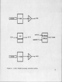
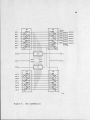
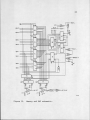
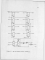
Figure 1.
Signal averager interface block diagram.
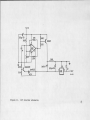
Figure 2.
Arithmetic logic unit section.
MD
BUS
MEM 0-15
►
Figure 3.
Memory section.
NWOVF
carv r
19 V
' m
12 V
^
-19 y
>
BLANKING
CIRCUIT
INVERTER
M A BUS Z
h
Y-H
AT
A
UA
v
z-BLANK
XOUT
>
Figure 4.
x and y digital-to-analog converter section.
LO
U>
BUS
LSI-11
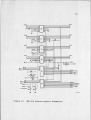
Figure 5.
Direct memory address and interrupt section.
DECODED BY BBS7
REGISTER
SELECTION
SWITCH SELECTABLE
17 16 15 14 13 12 II
10 9
8
7
6
5
4
3
2
AI2 All AIO A9 A8 A7 A6 A5 A4 A3
I
I
I
33-2 33-4
24-6 24-4 24-2
24-5
24-3 33-1
33-3 33-5
WCR =
BAR
=
CSR
=
DATIR DATOR
DEVICE ADDRESS
8
7
6
5
4
BYTE CONTROL
IXXXXO
IXXXX2
IXXXX4
|YYYYg
,XXXXb
INTERRUPT
SELECTION
3 2 1 0
V8 V7 V6 V5 V4 V3
1
1
1
24-1
33-7
33-9
33-6 33-8 33-10
INTERRUPT VECTOR
Figure 6
0
Device address and vector address format.
0
0
FIRST VECTOR = XXO
SECOND VECTOR = XX4
PRELIMINARY
LTS
~
SIGNAL
AVERAGER
UT I L I T Y
R C U T I HE3
11-JU N -7 ?
♦MCALL
•> ♦V 2 * * ? ♦REGDEF
♦MC A L L
♦P R I N I .v , D E V I C E ? ♦.P R 01" E C T ? , I H T E N :■ * H F P S * , MT
♦ ♦V 2 . ♦
, REGDEF
♦GL 0 B L S A I N I T ? S A B U F ? S A D P L Y ? S A E R 8 E , S A R S E T ? S A B E GN
♦GL OBL. S A ST AT ? S A F I L L ? S A S T 0 P >■S A S T R T ? S A S C A N r S A H A L T
SA$CSR=? 1 7 6 5 3 4
S A$ VE C = 3 3 0
P R I7=34 0
P R I5=5
y
♦D E V I C E . # A R E A y # D L I S T
, P R 0 T E CT * A R E A ># S A $ V E C
BC'S
2$
♦P R 01" E C I # A R E A ? # S A $ V E C r 4
BCS
2$
MOV
# SAX H v @# S A $ VE C
MOV
# P R 17? ® # S A $ V E C r 2
M0 V
* S A I H y is # S A $ V E C + 4
M0 V
# P R 1 7 ■/ 0 # S A * V E C + 6
CC C
2$ ♦
RTS
PC
AREA 5
♦BLKW
10,
♦WORD
SA$CSR ? 4 0 0 ? 0 •
DL 1 S T *
SADPLY 5 M0 V
@:il: S A $ C S R , S A C S R
J SR
PC y SARSET
BIS
# 0 0 0 1 0 0 * &# 3 A $ CSR
RTS
PC
0 * S A $ CS R , S A C 3 R
S A E R S E i M0 V
JSR
P C >SARSET
B IS
# 0 0 0 2 0 0 ?0 # SA $ CS R
B IT
# 0 0 0 2 0 0 ? Q# S A $ C S R
BNE
1$
J SR
PC y SARSET
M0 V
S A C S R f @# S A $ C S R /
RTS
PC
# 0 5 0 0 0 0 t Q* S A $ C S R
SARSETt B IC
BIS
# 0 0 0 4 0 0 ? @#SA$CSR
BIT
* 0 0 0 4 0 0 y 0?=11=S A $ CS R
BNE
1$
RTS
PC
S A P I L L ♦ M0 V
0 =11=S A $ C S R ? SAC S R
J SR
PC y SARSET
sabegn
:
Figure 7.
A simple interrupt handler routine.
MOV
TST
MOV
DEC
MOV
i*j
DEC
BNE
MOV
JSR
RTS
SASTAT: MOV
MOV
MOV
CLR
SEC
ROL
3 $:
BCS
♦PRINT
BIT.
BNE
*PRINT
BR
*PRINT
vat
ADD
2$:
BR
5$ 1
MOV
RTS
♦WORD
STATE i
♦ASCIZ
ms gi :
*ASCI2
MSG2 >
MSGBLKi ♦ASCII
♦WORD
♦ASCII
*WORD
♦ASCII
♦WORD
♦ASCII
♦WORD
♦ASCII
♦WORD
♦ASCII
♦WORD
♦ASCII
WORD
♦ASCII
♦WORD
♦ASCII
♦WORD
♦ASCII
♦WORD
♦ASCII
♦
RO?-< SP >
(R5)f
<R5)+ ?RO
RO
0(R5)+,0#SA$CSR
RO
1$
(SP)+ fRO
PC ySADPLY
PC
R2?-<SP)
0#SA$CSR ySACSR
#MSGBLK yR2
STATB
STATB
5$
R2
STATB r SACSR
1$
#MSG1
2$
#MSG2
#22 yR2
3$
(SP)+?R2
PC
0
NOT SET/
SET/
/ATTENTION FLAG /
100200
/SA DEVICE START /
100200
/DES TRUCTIV E REA D/
100200
/DOUBLE PRECISI0N/
100200
/XM ADDRESS 16
/
100200
/XM ADDRESS 17
100200
/MEMORY DISPLAY /
100200
/MEMORY ERASE
100200
/SA DEVICE RESET /
100200
/READ-MOD-WRITE /
100200
/DATA READ-OUT
/
Figure 7. Continued.
SA S T 0 P :
1$:
SA S T RT i
2$ J
1$:
MSGINT♦
S A IN IT ♦
SAREGI
SASCAN?
WC t
CSX
S A CS R ♦
SABUFP$
SABUF t
s a ih :
, WORD
, A S C11
♦WORD
♦A S C I I
♦WORD
♦ASCII
♦WORD
♦A S C11
♦WORD'
♦ASCII
♦WORD
♦EVEN
MOV
BIS
MOV
MOV
DEC
BNE
MOV
JSR
RTS
B IT
BNE
BIS
BIS
RTS
BIC
♦PRINT
BR ‘
* ASCIZ
♦EVEN
TST
MOV
MOV
M0 V
M0 V
RTS
♦WORD
* WORD
♦WORD
♦W0 R D
♦WORD
♦BLKW
♦INTEN
TST
BMI
B IT
BEG
J SR
J SR
100200
/ D MA R E QU E S T
100200
/DMA INTERRUPT E N /
100200
/DMA INTERRUPT
/
100200
/ E R R I N T E R R LJP T E N /•
100200
./ERR INTERRUPT
100200
0 =11=S A $ C S R ? S A C S R
* 0 0 0 0 0 1 f 0 # 3 A $ CSR
R4? - ( SP)
# 3 0 0 y R4
R4
1$
( S P ) + ? R4
PC ? SARSET
PC
# 1 2 0 0 0 0 ?0 # S A $ CS R
1$
# 0 5 0 0 0 0 ?0 # 8 A $ C3 R
# 0 0 0 0 0 2 7 0 # S A $ CSR
PC
# 1 2 0 0 0 0 7 0 # S A $ CS R
#MSGINT
2$
/ I N T E R R U P T I S SET?
( R5 ) +
0 ( R 5 ) + 7 SASCAN
WC ? 0#SA$ CSR™2
S A B iJ F P y Q# S A $ C 3 R - 4
C S 7 0 # b A $ CS R
PC
0
173777
002000
0
SABUF
4030
P R I5
0#SA$CSR
ATTN
# 2 0 0 0 0 7 0 # S A $ CS R
RET
PC 7 SARSET
PC 7 SAREG
Figure 7. Continued.
POSSIBLE
E RR OR /
DEC
BEG
J S ft
RTS
vJS R
ATTN t
RTS
MSGXXX £ ♦A S C I Z
♦EVEN
BIS
RET:
RTS
SAHALT * *MFPS
♦M I P S
JSR
SASCAN
S AH AL T
P C y S A S T ft T
PC
P C f b' A R SET
PC
< 15 > < 1 2 > / S C A N S C 0 MP L E T E / < 1 3 > < 12 > / * /
# 5 0 0 0 0 ? § # S A $ CS R
PC
#PR 1 7.
PC ? SARSET
♦PRINT fMSGXXX
♦MTPS
RTS
4 END
PC
Figure 7. Continued.
39
40
Figure 8.
ALU schematics.
41
ADD A 7
ADD A 0
DATA 7
MEM 7
DATA 0
MEM 0
DATA
MEM 15
51
56
17
DATA 8
COUT H ■
MEM 8
57
58
irn— itit
■1"I
'-rTf.ri'TT
2143 3 11132 6
121*3 5 11IS 26
ADD A 15
Figure 9.
ALU schematics.
ADD A 8
42
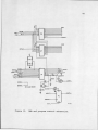
Figure 10.
Memory and DAC schematic.
+12 V
Figure 11.
12V inverter schematic.
u>
44
Figure 12.
DMA. and program control schematics.
O U TH B L
SELO L
INWD L
WCNTO H
DATIN L
BDM GO L
BDMR L
TD IN H
TSYNC H
RPLY H
ADREN L
BDMGI L
BDMGO L
RQSTB H
IN IT L -
Figure 13.
DMA and program control schematics.
46
sta r t
H
^ ^ 4 4 ^ 0 -9 ------------- DEVMAS L
CSRWHB H--------- H P * 0-4
DATA 15 -------------— ------IN IT H -
+5
1 00 0 p f 15K
HH
i T
+5
IK
ADREN H -
42
ATTN
r
„ ___ >—13-*---------- \ 12
SACYC H -------2 ^ 3 1 > > ------ r > > l 2
41
REQ H —
^ -----15-|p>0-5-------REPLY' H---------1
-(TOS + INIT) L
::E>"
S
5 -P > 0 -6 --------(T0S+INIT)H
CSRWHB
DATA
-RQSTA H
-DATIN L
OATA 10-------------INIT L ----------Jjj
40
S
-OATIO L
DATA 9 ---------1-
—n-> R
F
39
CSRWLB H-
-DATIOT L
+5
10K
USER RQST L 6
T
DATA 11--------2-
s
-B
40
43
DATNL-
-A
_u-----—.—
R
?
l
WCNTO H(TOS + INIT) H-
Figure 14.
DMA and program control schematics.
-5------------REQ H
INWD L-
DATEN L
SEL6 L-
DATEN H
25
DATN L -
-17
CHANHB H
MRPLY L .
OUTHB L '
•10
-C H A N LB H
r^3i
OUTLB LTDIN H-
DATEN H
ADREN H
TDOUTH
XM1T H
TRPLY H
INWD H
TRPLY H
TDIN H
r
i
i
i
i
i
i
i
i
i
i
i
i
i
i
TSYNC H---------------------- {■
i
i
i
i
TDOUT H --------------------- t'
i
i
MASTER H
Figure 15.
4^
16l
l5 - p
£
. 7
=
1
A-----------------•BRPLY
i
i
l -1----------------- RPLY H
1
I
■BDIN
I
l
_}-----------------■RDIN
1
i
I
l
I
1
l
H
■BSYNC
-RSYNC H
•BDOUT
1
l
H ----------------1
1
J
BSACK
DMA and program control schematics.
48
Figure 16.
DMA and program control schematics.
Figure 17.
DMA and program control schematics.
CIN
INIT
DEST L
X 1'
r.$ E >
-12J------ \
ERASEH
-8---------1H >
ha — DZERO
L
330
CHAN HB H ------- 9-1------\
+5
FLAG H -------- i-2 -| l8 > 0 -‘8
1 50 i
I
H
y
u R )o -
SUMCLR L
r8<XjiJ9— ‘
SUM LD L
13
■SUMEN L
l— 1►
-!-------DSTB LB H
CHAN LB --------------------- '
330
;
COUT-12
- DSTB HB H
3 30
’G > 5
1
SACYC
h7 = ! H > 6
68 pF <?3 9K
H84
_
TO IN H -
: M
: 2 0 0 pF
V
f*
,
SB-
SACYC L -
13
OW T HDATIO H— 12
MASTER
H
+ 5-
- ‘E > 4-
i|n>CM
6— DATLD H
I
£E >;
P G > -
CS L
WP L
+ 5-
i ® 0’
5 0 pF
P
75pF
75 pF
L rW
ADREN
x.1:
DATEN L DATEN H -
560
:H >
r l2i
-----f- 1 3 -l
-"j~ 22 0 pF
MACLKL
rW
i - 4 J ls > - 16—
WDC L
IN IT L
FP-6752
Figure 18.
Master controller schematic.
U1
O
Figure 19.
Master controller schematic.
cn
SA
INTERFACE
32 K x 16
MEMORY
LS I-11/2
CPU
I
0
5
LSI -11 BUS
DISK
CONTROLLER
4 SIO
“ f
t
/ <
A
PORTS
ft
V
FLOPPY
DIS K S
Figure 20.
GRAPHIC
TERMINAL
Total system configuration.
PLOTTER
ft
y
MODEM
PRINTER
53
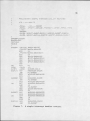
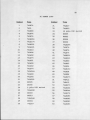
IC PARTS LIST
Number
1
2
3
4
5
6
7
8
9
10
11
12
13
14
15
16
17
18
19
20
21
22
23
24
25
26
27
28
29
30
Type
74LS74
7425
74LS00
74LS74
74LS74
74LS244
74LS174
74LS221
74LS221
74LS10
74LS04
74LS02
74LS74
74LS51
74LS00
74LS02
74LS74
74LS244
74LS00
74LS02
74LS221
DC005
DC005
5 pole DIP switch
74LS240
DC003
DC010
74LS240
DC0 04
74LS27
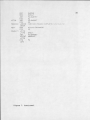
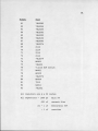
Number
31
32
33
34
35
36
37
38
39
40
41
42
43
44
45
46
47
48
49
50
51
52
53
54
55
56
57
58
59
60
Type
74LS27
74LS02
10 pole DIP switch
DC005
DC005
DC006
DC006
74LS244
74LS74
74LS74
74LS74
74LS221
74LS221
74LS00
74LS02
74LS04
74LS132
74LS28
74LS86
74LS273
74S412
74S412
74LS273
74LS244
74LS244
74LS374
74LS283
74LS283
74LS283
74LS283
54
Number
Type
61
62
63
64
65
66
67
68
69
74LS283
70
71
72
73
74
75
76
77
78
79
80
81
82
83
2114
2114
2114
74LS374
AD561
74LS02
4 pole DIP switch
AD561
AD509
74LS374
AD509
7912
LM311
74LS02
74LS244
74LS244
74LS393
74LS393
74LS132
74LS393
74LS374
2114
All resistors are h w 5% carbon
All capacitors < 1000 pf
.001 yf
.01 - 1 yf
> 1 yf
mica 5%
ceramic disc
monolythic 50V
tantalum