1
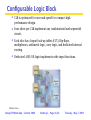
Meeting 2
Summer 2009 Doing DSP Workshop
Today:
◮
Comments.
◮
Joining a lab section.
◮
Introduce FPGAs and VHDL.
The modern computer hovers between the obsolescent and the nonexistent.
— Sydney Brenner, attributed in Science, 5 January 1990.
Doing DSP Workshop – Summer 2009
Meeting 2 – Page 1/64
Thursday – May 7, 2009
Workshop CD
◮
Workshop CD is rather full. Lots of relevant material.
◮
Most collections have an xxx.html (or the like) index file.
◮
A few don’t.
◮
Poke around. See what’s there. The collection is intended to
save you time and give some focus.
◮
There are two DSP oriented text books included.
Doing DSP Workshop – Summer 2009
Meeting 2 – Page 2/64
Thursday – May 7, 2009
Comments
◮
This is not a course. This is a workshop. Less structure, more
opportunity to participate, more opportunity to pursue one’s own
interests.
◮
Expect to have 6 lab exercises intended to familiarize you with
the Workshop hardware. One per week for six weeks.
◮
Following these exercises you have the opportunity to focus on
some aspect of DSP theory and/or implementation.
◮
The nominal end of the Workshop will be start of August, maybe
mid August, well, whenever.
◮
Discussion sessions Tu and Th 1:00 PM to 2:30 PM.
◮
The first six weeks of discussions will focus on labs. Some DSP
will be included.
◮
After six weeks will seek volunteers to research a topic and make
a minimum 20 minute presentation to the Workshop.
Doing DSP Workshop – Summer 2009
Meeting 2 – Page 3/64
Thursday – May 7, 2009
More comments
◮
We presently have about 28 Workshop members.
◮
The Workshop web page is at
www.eecs.umich.edu/courses/doing_dsp/
◮
A set of interesting questions can be found on the
Workshop web site. We will discuss them starting one week
from to day. This is NOT a homework assignment.
However, you might want to treat it as such.
◮
There are two lab sections, one Tuesday and one Thursday.
The max capacity is 18 students per section. This assumes
lab partners. Feel free to use off time.
◮
The first lab session will be next Tuesday.
◮
I will be out of town Friday through Monday.
Doing DSP Workshop – Summer 2009
Meeting 2 – Page 4/64
Thursday – May 7, 2009
First lab
Introduces the Spartan-3 Starter Board and VHDL.
◮
Have to start somewhere, some time.
◮
Read (not study) the Spartan-3 Starter Kit Board User Guide.
Can be found on the Workshop CD and on the Workshop
handouts web page.
◮
Find a VHDL tutorial and read (not study) it. I’ve put two
onto the handouts web page.
◮
Chih-Wei will be posting the first week lab write-up
probably on Monday. Probably on the handouts web page
or distributed by mailing list.
◮
There will help in lab. No deadline and no required lab
report. Though you might might want to sketch one out for
future reference.
Doing DSP Workshop – Summer 2009
Meeting 2 – Page 5/64
Thursday – May 7, 2009
A common lab exercise theme
Note that the MSP430 and the Piccolo possess at least one
channel of A/D conversion. Neither includes a D/A converter.
Kind of need to have a D/A converter if we are going to explore
computer generation of analog waveforms, e.g., sine wave.
◮
Will explore one-bit D/A conversion.
◮
Two methods, pulse width modulation and sigma-delta.
◮
What happen once we (re)enter the analog world will be of
interest as well.
◮
Will cheat with the S3SB and use a PMod D/A, at least at
first.
◮
Will be typically in the second week of each exercise pair.
◮
New to the coordinators as well.
Doing DSP Workshop – Summer 2009
Meeting 2 – Page 6/64
Thursday – May 7, 2009
Workshop mailing list
I’ve included everyone that I’m aware of. If you have not
received an email from me in the last two days you can add
yourself to the list.
For automatic subscriptions, send email to
[email protected]
with the subject as "Subscribe" or "Unsubscribe".
Note that you can remove yourself as well.
Doing DSP Workshop – Summer 2009
Meeting 2 – Page 7/64
Thursday – May 7, 2009
What defines a DSP microcomputer?
For years I’ve defined DSP microcomputer as a microcomputer
that possesses an instruction that multiplies two numbers
together and adds the result into an accumulator. A MAC
instruction.
Where does this leave microcomputers like the MSP430F2012?
It doesn’t even have a multiplier. However, it does have a 10-bit
A/D converter. It obviously is meant to do some sort of digital
signal processing.
Revised definition:
A DSP microcomputer is one whose instruction set
includes a multiply-and-accumulate (MAC) instruction
and/or possesses an A/D converter.
Doing DSP Workshop – Summer 2009
Meeting 2 – Page 8/64
Thursday – May 7, 2009
References
The best introduction to VHDL that I’ve seen is:
Circuit Design with VHDL, V. Pedroni ($29–$42).
The library copy appears to have been mis-shelved. I’ve put my
and Professor Stark’s copies on reserve.
Another good, reasonably priced book, is Advanced Digital
Logic Design by Sunggu Lee.
See the doing_dsp handouts web page for:
◮
ISE 10.1i Quick Start Tutorial.
◮
Programmable Logic Design Quick Start Handbook.
◮
Spartan-3 Starter Board User’s Guide.
◮
Chih-Wei’s ISE Tutorial.
Doing DSP Workshop – Summer 2009
Meeting 2 – Page 9/64
Thursday – May 7, 2009
What is an FPGA?
Field Programmable Gate Array
A programmable logic device that has lots of gates and other
special features that allow its “easy” use in digital systems.
Typically volatile, needs a boot device.
Xilinx introduced first FPGA devices in 1985. Best guess is that
there have been 6 or 7 generations. Current technology,
Virtex-5, is at the 65 nm level. The Spartan-3 devices used in the
lab are 90 nm.
Currently Xilinx has greater than 50% market share. 2008 net
revenue was $1.9 billion.
Costs are dropping, capabilities are rising.
Doing DSP Workshop – Summer 2009
Meeting 2 – Page 10/64
Thursday – May 7, 2009
Where FPGAs find use?
◮
Low volume (< 15k) applications.
◮
Where reconfigurability is important.
◮
Augmenting DSP chips.
◮
Replacing DSP chips.
◮
Software defined radios.
◮
Broadband modems.
◮
Set-top boxes.
◮
Auto-entertainment.
◮
Industrial automation.
◮
Many, many other applications.
Doing DSP Workshop – Summer 2009
Meeting 2 – Page 11/64
Thursday – May 7, 2009
The Xilinx Spartan-3 family devices
From the Xilinx web site.
Doing DSP Workshop – Summer 2009
Meeting 2 – Page 12/64
Thursday – May 7, 2009
Spartan-3 features
•
•
•
•
•
•
3.3V), and auxiliary purposes (2.5V)
SelectIO™ signaling
- Up to 784 I/O pins
- 622 Mb/s data transfer rate per I/O
- 18 single-ended signal standards
- 6 differential I/O standards including LVDS, RSDS
- Termination by Digitally Controlled Impedance
- Signal swing ranging from 1.14V to 3.45V
- Double Data Rate (DDR) support
Logic resources
- Abundant logic cells with shift register capability
- Wide multiplexers
- Fast look-ahead carry logic
- Dedicated 18 x 18 multipliers
- JTAG logic compatible with IEEE 1149.1/1532
SelectRAM™ hierarchical memory
- Up to 1,872 Kbits of total block RAM
- Up to 520 Kbits of total distributed RAM
Digital Clock Manager (up to four DCMs)
- Clock skew elimination
- Frequency synthesis
- High resolution phase shifting
Eight global clock lines and abundant routing
Fully supported by Xilinx ISE development system
From Xilinx Spartan-3 data manual
Doing DSP Workshop – Summer 2009
Meeting 2 – Page 13/64
Thursday – May 7, 2009
Configurable Logic Block
◮
CLB is optimized for area and speed for compact high
performance design.
◮
Four slices per CLB implement any combinatorial and sequential
circuit.
◮
Each slice has 4-input look-up tables (LUT), flip-flops,
multiplexors, arithmetic logic, carry logic, and dedicated internal
routing.
◮
Dedicated AND/OR logic implements wide input functions.
Xilinx web site.
Doing DSP Workshop – Summer 2009
Meeting 2 – Page 14/64
Thursday – May 7, 2009
Off fabric 18K bit memory blocks
WEA
ENA
SSRA
CLKA
ADDRA[rA–1:0]
DIA[wA–1:0]
DIPA[3:0]
RAM16_wA_wB
DOPA[pA–1:0]
DOA[wA–1:0]
WEB
ENB
SSRB
CLKB
ADDRB[rB–1:0]
DIB[wB–1:0]
DIPB[3:0]
DOPB[pB–1:0]
DOB[wB–1:0]
WE
EN
SSR
CLK
ADDR[r–1:0]
DI[w–1:0]
DIP[p–1:0]
(a) Dual-Port
S3E-100
S3-200
S3-1000
4 blocks
12 blocks
24 blocks
RAM16_Sw
DOP[p–1:0]
DO[w–1:0]
(b) Single-Port
72,728 bits
221,184 bits
442,368 bits
From Xilinx application note: XAPP463 V2.0.
Doing DSP Workshop – Summer 2009
Meeting 2 – Page 15/64
Thursday – May 7, 2009
Block RAM configurations
Total RAM bits, including parity
Memory Organizations
18,432 (16K data + 2K parity)
16Kx1
8Kx2
4Kx4
2Kx8 (no parity)
2Kx9 (x8 + parity)
1Kx16 (no parity)
1Kx18 (x16 + 2 parity)
512x32 (no parity)
512x36 (x32 + 4 parity)
256x72 (single-port only)
Parity
Performance
Timing Interface
Single-Port
Available and optional only for organizations greater than
byte-wide. Parity bits optionally available as extra data
bits.
200 MHz (estimated)
Simple synchronous interface. Similar to reading and
writing from a register with a setup time for write
operations and clock-to-output delay for read operations.
Yes
True Dual-Port
Yes
ROM, Initial RAM Contents
Yes
Mixed Data Port Widths
Power-Up Condition
Yes
User-defined data, defaults to zero
From Xilinx application note: XAPP463 V2.0.
Doing DSP Workshop – Summer 2009
Meeting 2 – Page 16/64
Thursday – May 7, 2009
Off fabric multipliers
Data Flow
Each embedded multiplier block (MULT18X18 primitive) supports two independent dynamic
data input ports: 18-bit signed or 17-bit unsigned. The two inputs are referred to as the
multiplicand and the multiplier, or the factors, while the output is the product. The MULT18X18
primitive is illustrated in Figure 1.
A [17:0]
P [35:0]
B [17:0]
MULT18X18
X467_01_032503
Figure 1: Embedded Multiplier
Can be configured as combinational or as registered. Timing depends
on the number of (lower) bits used in result. Note: 17-bit unsigned or
18-bit two’s complement.
From Xilinx application note: XAPP467.
Doing DSP Workshop – Summer 2009
Meeting 2 – Page 17/64
Thursday – May 7, 2009
Multiplier timing–using Core Generator
CLK
SCLR
RFD
RFD active unless ACLR or SCLR active
ND
new multiplier inputs A(n) & B(n)
A&B
Input
XXX XXX XXX XXX
A0
A1
An
A
n
A
n+1
interval depends on multiplier latency
RDY
new multiplier output
DOUT = 0 (SCLR was 1)
D0
DOUT
Dn
multiplier output still valid
but RDY low (ND was 0)
Dn
Dn+1
X467_07_040303
Figure 9: Multiplier Generator Timing Diagram
From Xilinx application note: XAPP467.
Doing DSP Workshop – Summer 2009
Meeting 2 – Page 18/64
Thursday – May 7, 2009
Routing–what makes it all happen
There are four types of wire segments available :
◮
general purpose segments,
the ones that pass through
switches in the switch block.
◮
Direct interconnect : ones
which connect logic block
pins to four surrounding
connecting blocks
◮
long line : high fan out
uniform delay connections
◮
clock lines : clock signal
provider which runs all over
the chip.
From http://www.tutorial-reports.com/computer-science/fpga/routing.php?PHPSESSID=9ed5dd1540f5b90fc4088f7c146
Doing DSP Workshop – Summer 2009
Meeting 2 – Page 19/64
Thursday – May 7, 2009
and when it happens
Global Clock Inputs
GCLK11 GCLK10
4
GCLK7
BUFGMUX
pair
DCM
•
X0Y8
2
Top Right
Quadrant (TR)
G
•
Top Spine
X0Y9
LHCLK6 LHCLK7
•
8
H
8
4
8
Left, Bottom
Top, Right
E
X3Y9 X3Y8
G
F
RHCLK3 RHCLK2
G
8
2
DCM
Clock
c Line
in Quadrant
DCM
4
H
Top Left
Quadrant (TL)
4
X2Y10 X2Y11
4
Top, Left
H
2
2
2
8
DCM
8
•
Left, Bottom
2
•
Bottom Spine
X0Y6 X0Y7
X0Y5
•
2
2
Note 4
8
Spine
Horizontal
Note 4
C
DCM
8
Note 3
8
8
•
XC3S1200E (X0Y2)
XC3S1600E (X0Y2)
8
Right Spine
D
C
2
8
8
•
DCM
2
X0Y2 X0Y3
4
8
4
D
2
B
Bottom Right
Quadrant (BR)
8
C
B
4
A
DCM
DCM
Bottom, Left
Bottom, Right
X1Y0 X1Y1
A
X3Y2
Bottom Left
Quadrant (BL)
•
X3Y3
•
B
RHCLK5 RHCLK4
LHCLK0 LHCLK1
2
Left, Top
2
2
A
E
X3Y5 X3Y4
X0Y4
Note 3
X3Y6
8
Left Spine
D
F
•
Right-Half Clock Inputs
E
•
X3Y7
LHCLK2 LHCLK3 LHCLK4 LHCLK5
2
F
RHCLK1 RHCLK0 RHCLK7 RHCLK6
Left-Half Clock Inputs
GCLK5 GCLK4
X1Y10 X1Y11
BUFGMUX
2
GCLK9 GCLK8
GCLK6
X2Y0 X2Y1
4
4
GCLK3 GCLK2
GCLK1 GCLK0
GCLK15 GCLK14
GCLK13 GCLK12
Global Clock Inputs
UG331_c4_02_080906
Notes:
From Xilinx UG331.pdf, Spartan-3 Generation FPGA User Guide (preliminary).
Doing DSP Workshop – Summer 2009
Meeting 2 – Page 20/64
Thursday – May 7, 2009
Digital Clock Multipliers
DCM
PSINCDEC
PSEN
PSCLK
Phase
Shifter
Delay Taps
Input Stage
Output Stage
CLK0
CLKIN
CLKFB
PSDONE
CLK90
CLK180
CLK270
CLK2X
CLK2X180
CLKDV
CLKFX
CLKFX180
DFS
DLL
Status
Logic
RST
Clock
Distribution
Delay
8
LOCKED
STATUS [7:0]
DS099-2_07_040103
Figure 3-3:
DCM Functional Block Diagram
From Xilinx UG331.pdf, Spartan-3 Generation FPGA User Guide (preliminary).
Doing DSP Workshop – Summer 2009
Meeting 2 – Page 21/64
Thursday – May 7, 2009
IO “standards”
“The nice things about standards is that there are so many of
them”.
S3
S3E
S3A
24 differential and single ended
18 differential and single ended
26 differential and single ended
Some restrictions apply.
Doing DSP Workshop – Summer 2009
Meeting 2 – Page 22/64
Thursday – May 7, 2009
The Spartan-3 die
From Xilinx
Doing DSP Workshop – Summer 2009
Meeting 2 – Page 23/64
Thursday – May 7, 2009
An INTEL figure
Doing DSP Workshop – Summer 2009
Meeting 2 – Page 24/64
Thursday – May 7, 2009
The Spartan-3 starter board
Basic unit (200K gates) sold
by Xilinx for $99.
Manufactured by Digilent.
Sells boards using 200K,
400K or 1M gate Spartan-3
for up to $149. Also sells
auxiliary boards such as
ethernet interface, 1 MHz
dual A/D and D/A, etc.
Well supported by Xilinx’s
free WebPack version of its
ISE 8.2 development
software.
Uses 50 MHz clock (can use
on-chip clock multiplier to
increase).
Photo and diagram from the Digilent web site.
Doing DSP Workshop – Summer 2009
Meeting 2 – Page 25/64
Thursday – May 7, 2009
FPGA boards in play in and about
EECS 452 is presently focused on Xilinx Spartan-3 FPGA devices
and is using starter/evaluation boards produced by Digilent.
◮
Spartan-3 1000 Starter Board. Used in lab.
◮
Spartan-3 200 Starter Board.
◮
Spartan-3 1000 Nexys Board.
◮
Spartan-3E 500 Nexys-2 Board.
◮
Spartan-3E 100 Basys board (2). .
◮
Virtex-2 Pro XUP. Available for project use. Xilinx donated.
◮
Nallatech uses Virtex-II 2V3000-4. Donated.
◮
Altera DE2 (as used in EECS 270).
◮
Spartan-3E 500 Starter Kit. .
These boards are reasonably “compatible” but not necessarily
without a bit of care and effort.
Doing DSP Workshop – Summer 2009
Meeting 2 – Page 26/64
Thursday – May 7, 2009
Digilent D/A, A/D and MIB
Digilent PmodDA2
Analog Outputs
D2
DAC121S101
D/A
Converter
ADC
1
Filter
P1
P2
P3: Data 2
ADC
2
Filter
P4: Clk
P3
P4
P5: GND
P5
P6: Vcc
P6
J2 Connector
Sync,
Clock
P2: Data1
J1 Connector
2
P1: CS
DAC121S101
D/A
Converter
J2 Connector
J1 Connector
D1
GND
AD1 Circuit Diagram
VCC
From Digilent data sheets.
Doing DSP Workshop – Summer 2009
Meeting 2 – Page 27/64
Thursday – May 7, 2009
Pmod in and out
◮
Pins on MIB connect to pins on PMOD modules.
◮
Use socket-socket cables to connect.
◮
Make sure VB on MIB connects to VCC on PMOD!
◮
Make connections with power OFF!
◮
Use 5 pin header on PMOD output so power is not present!
For now connector A1 is “not” being used. (Actually is
connected to memory bus which we will be using. Avoid using.
A2 is reserved for connecting to DSK peripheral interface bus.
B1 is left for use by other devices. EECS 452 attaches a MIB to
B1.
The Spartan-3 Starter Boards has provision for lots of
connections. This is the primary reason we chose it.
Doing DSP Workshop – Summer 2009
Meeting 2 – Page 28/64
Thursday – May 7, 2009
Lab arrangement
Doing DSP Workshop – Summer 2009
Meeting 2 – Page 29/64
Thursday – May 7, 2009
Xilinx tools
◮
ISE (we use the WebPACK version)
◮
◮
◮
◮
◮
Impact
◮
◮
◮
VHDL/Verilog/Schematic compiler
place and route
maps net list into FPGA
estimates timing
programs FPGA and/or EPROM.
has support for JTAG programmers.
ModelSim (by Mentor Graphics)
◮
simulates design
Digilent also sells programming cables and has associated
free programming software, ExPort.
Doing DSP Workshop – Summer 2009
Meeting 2 – Page 30/64
Thursday – May 7, 2009
Lab 1: VHDL, ISE and the S-3 Starter Board
◮
Demonstrates use of the:
◮
◮
◮
◮
◮
◮
◮
◮
Xilinx’s ISE and Impact tools,
VHDL,
slide switches,
push buttons (not physically debounced),
seven-segment displays,
individual LEDs,
serial RS-232 interface,
VGA output.
Be careful! Don’t let the smoke out!
Doing DSP Workshop – Summer 2009
Meeting 2 – Page 31/64
Thursday – May 7, 2009
Hardware Description Languages
Originally developed to simulate designs. However, you probably
should build what you simulate so they also became implementation
languages as well.
Verilog — used in Engin 100, EECS 270 and . . .
◮
Simple data types.
◮
Relatively easier to learn.
◮
Will guess at what you meant.
VHDL — used in EECS 452
◮
Strongly typed.
◮
Less easily learned.
◮
Makes you say what you mean and mean what you say.
“Synthesizable” means that a description can be made into hardware.
Doing DSP Workshop – Summer 2009
Meeting 2 – Page 32/64
Thursday – May 7, 2009
Why use an HDL?
◮
allows modularization, encapsulation, information hiding.
◮
parameters essentially map into physical connections.
◮
checks for errors and inconsistencies.
◮
enhances designer productivity (really!).
◮
working at a level closer to the device is probably
overwhelming.
VHDL supports functional and structural models.
Doing DSP Workshop – Summer 2009
Meeting 2 – Page 33/64
Thursday – May 7, 2009
What is Xilinx WebPACK ISE?
In lab we are using Xilinx’s WebPACK ISE 10.1 with SP3.
Free subset of ISE Foundation (very good and sort of expensive).
An integrated system design environment.
◮
Design entry – schematic, VHDL, Verilog.
◮
Generation of FPGA bit file.
◮
Simulation support.
◮
Fits and routes design.
Includes Impact. . . device programmer.
◮
◮
◮
◮
◮
Converts bit to various files.
Loads programming into devices.
Programs.
And much, much, more!
Doing DSP Workshop – Summer 2009
Meeting 2 – Page 34/64
Thursday – May 7, 2009
FPGA computers from Xilinx
◮
PicoBlaze — 8-bit, tiny.
Distributed as VHDL. Very useful. Good starting point.
◮
MicroBlaze — 32-bit, Unix able, on-fabric.
Need EDX (he have). Distributed as net list? Pretty much
full featured.
◮
PowerPC — 32-bit, off fabric, integer.
Need EDK (we have). Two projects have used. FPU available
as add on.
Doing DSP Workshop – Summer 2009
Meeting 2 – Page 35/64
Thursday – May 7, 2009
PicoBlaze System
Key Feature Set*
PicoBlaze Instruction Set*
• 16 byte-wide general-purpose data registers
• 1K instructions of programmable on-chip program store, automatically
loaded during FPGA configuration
• Byte-wide Arithmetic Logic Unit (ALU) with CARRY and ZERO
indicator flags
• 64-byte internal scratchpad RAM
• 256 input and 256 output ports for easy expansion and enhancement
• Automatic 31-location CALL/RETURN stack
• Predictable performance, always two clock cycles per instruction,
up to 200 MHz or 100 MIPS in a Virtex-4 ™ FPGA and 88 MHz
or 44 MIPS in a Spartan-3 FPGA
• Fast interrupt response; worst-case 5 clock cycles
• Assembler, instruction-set simulator support
PicoBlaze Block Diagram*
Take the Next Step
Visit www.xilinx.com/picoblaze to download the free PicoBlaze
microcontroller reference design, which includes the PicoBlaze
VHDL source code, assembler, and related documentation.
*Based on PicoBlaze for Spartan-3,Virtex-II/Pro and Virtex-4 (KCPSM3).
From Xilinx brochure.
Doing DSP Workshop – Summer 2009
Meeting 2 – Page 36/64
Thursday – May 7, 2009
MicroBlaze System
From Xilinx brochure.
Doing DSP Workshop – Summer 2009
Meeting 2 – Page 37/64
Thursday – May 7, 2009
IBM PowerPC
External Bus Interface
MMU
PowerPC
405 CPU
PCI
Bridge
Ext. Bus
Master Ctr
RAM/ROM/
PCMCIA
Controller
SDRAM
Controller
ATM 622 SAR
Code Decompression
PLB
Timers
Ethernet
Arbiter
Arbiter
OPB
HDLC
HDLC
HDLC
4KB
SRAM
UART
APU
UART
Interrupt
Control
GPIO
OCM
Control
DMA
Controller
OPB
Bridge
PowerPC 405x3
Embedded Core
From IBM brochure.
USB
Trace
I2C
JTAG
MAL
HDLC
I-Cache
D-Cache
Figure 2. Example 405x3 core+ASIC
Doing DSP Workshop – Summer 2009
Meeting 2 – Page 38/64
Thursday – May 7, 2009
VHDL background
◮
Hardware design/simulation language.
◮
Supports structural and behavior design description.
Logic units are called entities.
◮
◮
◮
port description. . . visible connections,
architecture. . . the design, internal signal definitions.
◮
DoD initiated. . . ADA like.
◮
Strongly typed.
◮
Picky, picky, picky.
◮
Mostly used in Universities, DoD, East Coast, Europe.
Doing DSP Workshop – Summer 2009
Meeting 2 – Page 39/64
Thursday – May 7, 2009
Entities are connectable logic blocks
Outside world
pins
FPGA
constraints
entity
port
architecture
process
process
Doing DSP Workshop – Summer 2009
Meeting 2 – Page 40/64
Thursday – May 7, 2009
The design description hierarchy
íÜÉ=êÉ~ä=ïçêäÇ
Ü~êÇï~êÉ
Åçåëíê~áåí=ÑáäÉ
íçé=äÉîÉä
ÇçáåÖ=ëçãÉíÜáåÖ=ìëÉÑìä
cmd^=~åÇ=ïÜ~íÉîÉê=áí
áë=ÅçååÉÅíÉÇ=íç
ã~éë=ëáÖå~äë=íç cmd^=éáåë
ÅçååÉÅíë=ã~àçê=ÇÉëáÖå=ìåáíë
ÇÉÅêÉ~ëáåÖ=äÉîÉä=çÑ=~Äëíê~Åíáçå
åáííóJÖêáííó
Doing DSP Workshop – Summer 2009
Meeting 2 – Page 41/64
Thursday – May 7, 2009
Example: binary addition
Consider adding two 8-bit values a and b
+
a7
a6
a5
a4
a3
a2
a1
a0
b7
b6
b5
b4
b3
b2
b1
b0 .
For each bit position we form the sum of the two bits in that
position and add in any carry from the previous (lower index)
bit position. The carry into position 1 is 0.
c7
+
c7
c6
c5
c4
c3
c2
c1
c0
0
a7
a6
a5
a4
a3
a2
a1
a0
b7
b6
b5
b4
b3
b2
b1
b0
s7
s6
s5
s4
s3
s2
s1
s0
Doing DSP Workshop – Summer 2009
Meeting 2 – Page 42/64
Thursday – May 7, 2009
A single bit adder unit
outputs
inputs
cn
sn
bn
an
cn−1
0
0
0
0
0
0
1
0
0
1
0
1
0
1
0
1
0
0
1
1
0
1
1
0
0
1
0
1
0
1
1
0
1
1
0
1
1
1
1
1
Doing DSP Workshop – Summer 2009
Åçìí
Å~êêó
Åáå
~
Ä
Meeting 2 – Page 43/64
ë
ëìã
Thursday – May 7, 2009
VHDL – behavioral
use IEEE.STD_LOGIC_1164.ALL;
use IEEE.STD_LOGIC_ARITH.ALL;
use IEEE.STD_LOGIC_UNSIGNED.ALL;
entity FullAdder01 is
Port ( a : in STD_LOGIC;
b : in STD_LOGIC;
cin : in STD_LOGIC;
sum : out STD_LOGIC;
cout : out STD_LOGIC);
end FullAdder01;
architecture Behavioral of FullAdder01 is
begin
sum <= a xor b xor cin;
cout <= (a and b) or (cin and a) or (cin and b);
end Behavioral;
Doing DSP Workshop – Summer 2009
Meeting 2 – Page 44/64
Thursday – May 7, 2009
Basic VHDL entity
◮
◮
This defines a “black box”, entity.
There is a port into/outof the box/entity.
◮
◮
There are three input signals: a, b, c_in.
There are two output signals: sum, c_out.
◮
Externally the contents of the box are hidded.
◮
In effect it simply works.
◮
Associated with the entity port is a description of how it
works, the entity’s architecture.
The architecture
◮
◮
◮
◮
defines the internal signals.
describes what the entity does in order to go from input to
output.
For this example, everything happens all at once.
Doing DSP Workshop – Summer 2009
Meeting 2 – Page 45/64
Thursday – May 7, 2009
An application
Classroom one-bit adder demonstration.
Three slide switches for input. Two LEDs for display.
Allows student to compare logic design operation against truth
table.
Ä
~
Åáå
Doing DSP Workshop – Summer 2009
íçé
cmd^
~ÇÇÉê
Éåíáíó
Åçìí
ëìã
Meeting 2 – Page 46/64
Thursday – May 7, 2009
Top level
◮
Usually use a top level to connect various module at the top level.
◮
Normally will not do any logic at this level. Only connect modules.
◮
Top’s port connects to the FPGA I/O pins.
◮
A xxxx.ucf file is used to attach names to the FPGA pins.
◮
Pins are attached to external hardware by printed circuit.
entity AdderDemoTop is
Port ( swt : in STD_LOGIC_VECTOR (2 downto 0);
led : out STD_LOGIC_VECTOR (1 downto 0));
end AdderDemoTop;
architecture Behavioral of AdderDemoTop is
begin
onebitadd : entity work.FullAdder01
port map( a => swt(1), b => swt(2), cin => swt(0),
sum => led(0), cout => led(1));
end Behavioral;
Doing DSP Workshop – Summer 2009
Meeting 2 – Page 47/64
Thursday – May 7, 2009
Connecting to the hardware
◮
We have set up a default .ucf file. Except for the clock all
name assignments are commented out. Uncomment only
those used for a given project.
◮
Use the names defined in the .ucf file as top’s port signal
names.
◮
When combining self contained modules that already have
a top use a toptop to connect modules. For example an
OFDM receiver with the XVGA support.
# light emitting
#
NET "led<0>" LOC
NET "led<1>" LOC
#
# slide switches
#
NET "swt<0>" LOC
NET "swt<1>" LOC
NET "swt<2>" LOC
diodes
= "K12" | IOSTANDARD = LVCMOS33;
= "P14" | IOSTANDARD = LVCMOS33;
= "F12" | IOSTANDARD = LVCMOS33;
= "G12" | IOSTANDARD = LVCMOS33;
= "H14" | IOSTANDARD = LVCMOS33;
Doing DSP Workshop – Summer 2009
Meeting 2 – Page 48/64
Thursday – May 7, 2009
Ripple carry adder
Having a one-bit adder we can use it to make an N-bit adder.
ÄT ~ T
ÅT
ÄS ~ S
ÅS
ëT
ÄR ~ R
ÅR
ëS
ÄQ ~ Q
ÅQ
ëR
ÄP ~ P
ÅP
ëQ
ÄO ~ O
ÅO
ëP
ÄN ~ N
ÅN
ëO
ÄM ~ M
ÅM
ëN
M
ëM
Execution time limited by the time required for carries to
propagate from least significant bit to most significant bit..
Can reduce propagation time by incorporating carry lookahead
logic. However this comes with a cost in terms of increased gate
count. Knowing how to do this is where the pros start to earn
their money.
Doing DSP Workshop – Summer 2009
Meeting 2 – Page 49/64
Thursday – May 7, 2009
Bit serial addition
The basic element is a one-bit full adder with the carry bit fed back
through a register. Values are shifted through the adder starting least
significant bit first.
Å~êêó
ê
~
Ä
ò
êÉëÉí
ëìã
ë
To subtract invert the bits of the value being subtracted and initialize
the carry bit to one.
Doing DSP Workshop – Summer 2009
Meeting 2 – Page 50/64
Thursday – May 7, 2009
Bit serial adder
ãëÄ
~
äëÄ
Ä
ëÜáÑí=êÉÖáëíÉêë
NJÄáí=~ÇÇÉê
ãëÄ
ë
äëÄ
ëÜáÑí=êÉÖáëíÉê
Åçìí
Åáå
a
áåáíá~äáòÉ
íç=M
Minimal logic. Can be clocked at high rates.
Execution time strongly influenced by word size.
Not shown is the control logic needed to step the operation.
This might be as simple as a counter. The point is that this
extra logic is not shown.
Doing DSP Workshop – Summer 2009
Meeting 2 – Page 51/64
Thursday – May 7, 2009
VHDL for bit serial adder
library IEEE;
use IEEE.STD_LOGIC_1164.ALL;
use IEEE.STD_LOGIC_ARITH.ALL;
use IEEE.STD_LOGIC_UNSIGNED.ALL;
entity BitSerialAdder is
Port ( a : in std_logic;
b : in std_logic;
clear : in std_logic;
clk : in std_logic;
ce : in std_logic;
sum : out std_logic);
end BitSerialAdder;
architecture Behavioral of BitSerialAdder is
signal sum_internal:std_logic;
signal carry_in:std_logic;
signal carry:std_logic;
begin
bit_sum:process(clear, clk) is begin
sum_internal <= a xor b xor carry_in;
carry <= (a and carry_in) or (b and carry_in) or (a and b);
if (clear = ’1’) then
sum
<= ’0’;
carry_in <= ’0’;
elsif (rising_edge(clk)) then
if (ce=’1’) then
sum <= sum_internal;
carry_in <= carry;
end if;
end if;
end process bit_sum;
end Behavioral;
Doing DSP Workshop – Summer 2009
Meeting 2 – Page 52/64
Thursday – May 7, 2009
Comments
◮
Up to this point we have been using combinational logic.
◮
The bit serial adder introduces the use of sequential logic.
◮
VHDL’s concept of sequential differs SIGNIFICANTLY from
of that one thinks of as sequential when programming in a
language such as C.
◮
Sequential statements have to be placed within a process
block.
Doing DSP Workshop – Summer 2009
Meeting 2 – Page 53/64
Thursday – May 7, 2009
Becoming proficient
Sort of like playing the piano. You might
◮
be born meant to play it. It’s in your body and soul.
◮
be good at it.
◮
be competent but not brilliant.
◮
have to work hard to get an audience.
◮
start looking for something else to do.
Becoming accomplished and successful requires desire, effort
and practice, practice, . . . .
Doing DSP Workshop – Summer 2009
Meeting 2 – Page 54/64
Thursday – May 7, 2009
A small digression
There exist families of binary sequences that possess periodic two-level
autocorrelation functions. With proper processing the amount of energy
contained in a full period can be collapsed into a single bit duration. An L-bit
sequence has the potential to increase detection by 10 log(L) dB. These
sequences are commonly used in communications systems.
Magnitude of the output of FPGA
correlator via a PicoBlaze test
processor. UART used to send
formatted values to TeraTerm
Tektronix 4100 emulator. Top plot is
real part, bottom plot is imaginary
part. The startup transient is seen at
the left. Once a full period has been
acquired the non-peak values are equal
to -1.
Doing DSP Workshop – Summer 2009
Meeting 2 – Page 55/64
Thursday – May 7, 2009
Implementing a bit serial correlator
FPGA implementation adds/subtracts 63 complex values using a nominal 20
clock tics.
Bit serial sliding pn-correlator unit.
Cut 1, rev 0 12July2005
load
sample from
external source
sample from
external source
16
SR125
16
SR124
SR123
SR2
SR1
only even stages are connected to subtract unit
control
SR0
0
32 bit-serial subtract units
16 bit-serial add units
Subtract/ add network
for
imaginary part
8 bit-serial add units
4 bit-serial add units
2 bit-serial add units
1 bit-serial add unit
18-bit values produced
then rounded to 16-bits
output
16
16
done
Doing DSP Workshop – Summer 2009
Meeting 2 – Page 56/64
Thursday – May 7, 2009
Another example project
This is for the Basys. The only files that really needing to be
changed for the S3-Starter Board should be the constraint file.
Oops, also have to specify the correct FPGA part and package to
ISE.
The task is to use the slide switches to turn on and off
individual segments (and the dp) on the right most seven
segment digit.
This is a purely combinational project and is intended to give
practise using the tools.
Digilent’s Basys Version C board used the 3E-100 TQ100 part
while the current Version E board uses the 3E-100 TQ144 part.
Doing DSP Workshop – Summer 2009
Meeting 2 – Page 57/64
Thursday – May 7, 2009
Basys board’s devices. . . S3SB is similar
3.3V
15
12
10
9
5
4
3
2
69
BTN0
30
BTN1
13
BTN2
11
BTN3
3.3V
SW0
Slide
switches
95
SW2
94
SW3
92
SW4
91
SW5
90
SW6
89
SW7
88
LD1
LEDs
LD3
LD4
LD5
LD6
LD7
3.3V
98
SW1
LD0
LD2
33
32
27
26
AN1
AN2
AN3
AN4
Spartan 3E
FPGA
42
24
22
17
16
43
23
18
CA
CB
Sseg
Display
CC
CD
CE
CF
CG
DP
From Digilent Basys Version C user manual.
Doing DSP Workshop – Summer 2009
Meeting 2 – Page 58/64
Thursday – May 7, 2009
Seven segment detail. . . S3SB similar
Common anode
AN1
AN2
AN3
AN4
A
F
CA CB CC CD CE CF CG DP
G
E
B
C
DP
Four-digit Seven
Segment Display
D
Individual cathodes
From Digilent Basys Version C user manual.
Doing DSP Workshop – Summer 2009
Meeting 2 – Page 59/64
Thursday – May 7, 2009
My simple 7-segment test VHDL
library IEEE;
use IEEE.STD_LOGIC_1164.ALL;
use IEEE.STD_LOGIC_ARITH.ALL;
use IEEE.STD_LOGIC_UNSIGNED.ALL;
entity top_seven_segment is
Port ( ssg : out STD_LOGIC_VECTOR (7 downto 0);
an : out STD_LOGIC_VECTOR (3 downto 0);
swt : in STD_LOGIC_VECTOR (7 downto 0));
end top_seven_segment;
architecture Behavioral of top_seven_segment is
signal sw_in : std_logic_vector(7 downto 0);
signal ssg_out : std_logic_vector(7 downto 0);
begin
an <= "1110";
sw_in <= not swt; -ssg_out <= sw_in; -ssg <= ssg_out(7) &
ssg_out(3) &
end Behavioral;
Doing DSP Workshop – Summer 2009
complement switch bit pattern
connect switches directly to segments
ssg_out(6) & ssg_out(5) & ssg_out(4) &
ssg_out(2) & ssg_out(1) & ssg_out(0);
Meeting 2 – Page 60/64
Thursday – May 7, 2009
My UCF
# seven segment digit anodes
NET "an<0>" LOC = "P34" | IOSTANDARD
NET "an<1>" LOC = "P33" | IOSTANDARD
NET "an<2>" LOC = "P32" | IOSTANDARD
NET "an<3>" LOC = "P26" | IOSTANDARD
# seven segment digit cathodes
NET "ssg<0>" LOC = "P83" | IOSTANDARD
NET "ssg<1>" LOC = "P17" | IOSTANDARD
NET "ssg<2>" LOC = "P20" | IOSTANDARD
NET "ssg<3>" LOC = "P21" | IOSTANDARD
NET "ssg<4>" LOC = "P23" | IOSTANDARD
NET "ssg<5>" LOC = "P16" | IOSTANDARD
NET "ssg<6>" LOC = "P25" | IOSTANDARD
NET "ssg<7>" LOC = "P22" | IOSTANDARD
# slide switches
NET "swt<0>" LOC = "P38" | IOSTANDARD
NET "swt<1>" LOC = "P36" | IOSTANDARD
NET "swt<2>" LOC = "P29" | IOSTANDARD
NET "swt<3>" LOC = "P24" | IOSTANDARD
NET "swt<4>" LOC = "P18" | IOSTANDARD
NET "swt<5>" LOC = "P12" | IOSTANDARD
NET "swt<6>" LOC = "P10" | IOSTANDARD
NET "swt<7>" LOC = "P6" | IOSTANDARD
=
=
=
=
LVCMOS33; # left most digit
LVCMOS33;
LVCMOS33;
LVCMOS33; # right most digit
=
=
=
=
=
=
=
=
LVCMOS33;
LVCMOS33;
LVCMOS33;
LVCMOS33;
LVCMOS33;
LVCMOS33;
LVCMOS33;
LVCMOS33;
=
=
=
=
=
=
=
=
LVCMOS33; # right most slide switch
LVCMOS33;
LVCMOS33;
LVCMOS33;
LVCMOS33;
LVCMOS33;
LVCMOS33;
LVCMOS33; # left most slide switch
#
#
#
#
#
#
#
#
segment
segment
segment
segment
segment
segment
segment
decimal
G
F
E
D
C
B
A
point
Note: this is for the Basys-E board (current version)!
Doing DSP Workshop – Summer 2009
Meeting 2 – Page 61/64
Thursday – May 7, 2009
Xilinx ISE
◮
GUI entry system and design compiler.
◮
Supports graphical and text inputs.
◮
Does immense amount of work going from description to
bit file.
Doing DSP Workshop – Summer 2009
Meeting 2 – Page 62/64
Thursday – May 7, 2009
Xilinx Impact
◮
Used to program FPGAs and PROMs.
◮
Use parallel-cable.
◮
Converts bit file to xxx.
Doing DSP Workshop – Summer 2009
Meeting 2 – Page 63/64
Thursday – May 7, 2009
Digilent Export
◮
Used to program FPGAs and PROMs.
◮
Part of Digilent’s Adept software.
◮
Works with all boards via parallel-cable.
◮
ISE does not recognize Digilent USB cables.
◮
Really easy to use.
◮
Use bit file for the FPGA.
◮
Needs xxx file for the ROM.
Doing DSP Workshop – Summer 2009
Meeting 2 – Page 64/64
Thursday – May 7, 2009