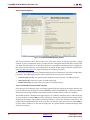
1
LogiCORE IP Block
Memory Generator v6.1
DS512 March 1, 2011
Product Specification
Introduction
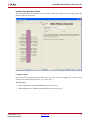
LogiCORE IP Facts
The Xilinx LogiCORE™ IP Block Memory Generator
(BMG) core is an advanced memory constructor that
generates area and performance-optimized memories
using embedded block RAM resources in Xilinx
FPGAs. Available through the CORE Generator™
software, users can quickly create optimized memories
to leverage the performance and features of block
RAMs in Xilinx FPGAs.
Core Specifics
Supported
Device Family (1)
Kintex-7, Virtex-7, Virtex-6, Virtex-5,
Virtex-4, Spartan-6, Spartan-3E/XA,
Spartan-3/XA, Spartan-3A/3AN/3A DSP
Supported User
Interfaces
AXI4, AXI4-Lite
Block RAM
Varied, based on core parameters
DCM
None
BUFG
None
IOBs/
Transceivers
None
The Native interface BMG core configurations support
the same standard BMG functions delivered by
previous versions of the Block Memory Generator (up
to and including version 4.3). Port interface names are
identical.
PPC
None
The AXI4 interface configuration of the BMG core is
derived from the Native interface BMG configuration
and adds an industry-standard bus protocol interface
to the core. Two AXI4 interface styles are available:
AXI4 and AXI4-Lite.
Design File
Formats
The BMG core supports both Native and AXI4
interfaces.
IOB-FF/TBUFs
None
Provided with Core
Product Specification
Migration Guide (2)
Documentation
NGC Netlist
Design Tool Requirements
Xilinx
Implementation
Tools
For details on the features of each interface, see
Features.
Simulation
ISE v13.1
Mentor Graphics ModelSim v6.6d
VHDL Structural
Verilog Structural
VHDL Behavioral (3)
Verilog Behavioral (3)
Synthesis
XST
Support
Provided by Xilinx, Inc.
1. For the complete list of supported devices, see Table 1, page 3 and
the release notes for this core.
2. The Migration Guide provides instructions for converting designs
that contain instances of either Legacy LogiCORE IP 6.x Single or
Dual Port Block Memory, or older versions of the Block Memory
Generator to the latest version of the Block Memory Generator.
3. Behavioral models do not precisely model collision behavior. See
Simulation Models, page 55 for details.
© 2006–2011 Xilinx, Inc. XILINX, the Xilinx logo, Kintex, Virtex, Spartan, ISE and other designated brands included herein are trademarks of Xilinx in the United
States and other countries. All other trademarks are the property of their respective owners.
DS512 March 1, 2011
Product Specification
www.xilinx.com
1
LogiCORE IP Block Memory Generator v6.1
Features
Features Common to the Native Interface and AXI4 BMG Cores
•
Optimized algorithms for minimum block RAM resource utilization or low power utilization
•
Configurable memory initialization
•
Individual Write enable per byte in Kintex™-7, Virtex®-7, Virtex-6, Virtex-5, Virtex-4, Spartan®-6,
and Spartan-3A/XA DSP with or without parity
•
Optimized VHDL and Verilog behavioral models for fast simulation times; structural simulation
models for precise simulation of memory behaviors
•
Selectable operating mode per port: WRITE_FIRST, READ_FIRST, or NO_CHANGE
•
Smaller fixed primitive configurations are now possible in Spartan-6 devices with the introduction
of the new Spartan-6 device 9K primitives
•
Lower data widths for Kintex-7, Virtex-7, and Virtex-6 devices in SDP mode
Native Block Memory Generator Specific Features
•
Generates Single-port RAM, Simple Dual-port RAM, True Dual-port RAM, Single-port ROM, and
Dual-port ROM
•
Supports data widths from 1 to 1152 bits and memory depths from 2 to 9M words (limited only by
memory resources on selected part)
•
Configurable port aspect ratios for dual-port configurations and Read-to-Write aspect ratios in
Virtex-6, Virtex-5, and Virtex-4 FPGAs
•
Supports the built-in Hamming Error Correction Capability (ECC) available in Kintex-7, Virtex-7,
Virtex-6 and Virtex-5 devices for data widths greater than 64 bits. Error injection pins in Kintex-7,
Virtex-7, and Virtex-6 allow insertion of single and double-bit errors
•
Supports soft Hamming Error Correction (Soft ECC) in Kintex-7, Virtex-7, Virtex-6, and Spartan-6
devices for data widths less than 64 bits.
•
Option to pipeline DOUT bus for improved performance in specific configurations
•
Choice of reset priority for output registers between priority of SR (Set Reset) or CE (Clock Enable)
in Kintex-7, Virtex-7, Virtex-6, and Spartan-6 families
•
Asynchronous reset in Spartan-6 devices
•
Performance up to 450 MHz
AXI4 Interface Block Memory Generator Specific Features
2
•
Supports AXI4 and AXI4-Lite interface protocols
•
AXI4 compliant Memory and Peripheral Slave types
•
Independent Read and Write Channels
•
Zero delay datapath
•
Supports registered outputs for handshake signals
•
INCR burst sizes up to 256 data transfers
•
WRAP bursts of 2, 4, 8, and 16 data beats
•
AXI narrow and unaligned burst transfers
•
Simple Dual-port RAM primitive configurations
•
Performance up to 300 MHz
www.xilinx.com
DS512 March 1, 2011
Product Specification
LogiCORE IP Block Memory Generator v6.1
•
Supports data widths from up to 256 bits and memory depths from 2 to 9 M words (limited only
by memory resources on selected part)
•
Symmetric aspect ratios
•
Asynchronous active low reset
Native Block Memory Generator Feature Summary
Overview
The Block Memory Generator core uses embedded Block Memory primitives in Xilinx FPGAs to extend
the functionality and capability of a single primitive to memories of arbitrary widths and depths.
Sophisticated algorithms within the Block Memory Generator core produce optimized solutions to
provide convenient access to memories for a wide range of configurations.
The Block Memory Generator has two fully independent ports that access a shared memory space. Both
A and B ports have a Write and a Read interface. In Kintex-7, Virtex-7, Virtex-6, Virtex-5 and Virtex-4
FPGA architectures, each of the four interfaces can be uniquely configured with a different data width.
When not using all four interfaces, the user can select a simplified memory configuration (for example,
a Single-Port Memory or Simple Dual-Port Memory) to reduce FPGA resource utilization.
The Block Memory Generator is not completely backward-compatible with the discontinued legacy
Single-Port Block Memory and Dual-Port Block Memory cores; for information about the differences,
see Compatibility with Older Memory Cores, page 86.
Applications
The Block Memory Generator core is used to create customized memories to suit any application.
Typical applications include:
•
Single-port RAM: Processor scratch RAM, look-up tables
•
Simple Dual-port RAM: Content addressable memories, FIFOs
•
True Dual-port RAM: Multi-processor storage
•
Single-port ROM: Program code storage, initialization ROM
•
Dual-port ROM: Single ROM shared between two processors/systems
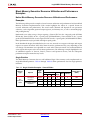
Supported Devices
Table 1 shows the families and sub-families supported by the Block Memory Generator.
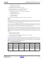
Table 1: Supported FPGA Families and Sub-Families
FPGA Family
Sub-Family
Spartan-3
Spartan-3E
Spartan-3A
Spartan-3AN
Spartan-3A DSP
Spartan-6
LX/LXT
Virtex-4
LX/FX/SX
DS512 March 1, 2011
Product Specification
www.xilinx.com
3
LogiCORE IP Block Memory Generator v6.1
Table 1: Supported FPGA Families and Sub-Families (Cont’d)
FPGA Family
Sub-Family
Virtex-5
LXT/FXT/SXT/TXT
Virtex-6
CXT/HXT/LXT/SXT
Virtex-7
Kintex-7
Memory Types
The Block Memory Generator core uses embedded block RAM to generate five types of memories:
•
Single-port RAM
•
Simple Dual-port RAM
•
True Dual-port RAM
•
Single-port ROM
•
Dual-port ROM
For dual-port memories, each port operates independently. Operating mode, clock frequency, optional
output registers, and optional pins are selectable per port. For Simple Dual-port RAM, the operating
modes are not selectable. See Collision Behavior, page 30 for additional information.
Selectable Memory Algorithm
The core configures block RAM primitives and connects them together using one of the following
algorithms:
•
Minimum Area Algorithm: The memory is generated using the minimum number of block RAM
primitives. Both data and parity bits are utilized.
•
Low Power Algorithm: The memory is generated such that the minimum number of block RAM
primitives are enabled during a Read or Write operation.
•
Fixed Primitive Algorithm: The memory is generated using only one type of block RAM
primitive. For a complete list of primitives available for each device family, see the data sheet for
that family.
Configurable Width and Depth
The Block Memory Generator can generate memory structures from 1 to 1152 bits wide, and at least two
locations deep. The maximum depth of the memory is limited only by the number of block RAM
primitives in the target device.
Selectable Operating Mode per Port
The Block Memory Generator supports the following block RAM primitive operating modes: WRITE
FIRST, READ FIRST, and NO CHANGE. Each port may be assigned its own operating mode.
Selectable Port Aspect Ratios
The core supports the same port aspect ratios as the block RAM primitives:
•
4
In all supported device families, the A port width may differ from the B port width by a factor of 1,
2, 4, 8, 16, or 32.
www.xilinx.com
DS512 March 1, 2011
Product Specification
LogiCORE IP Block Memory Generator v6.1
•
In Kintex-7, Virtex-7, Virtex-6, Virtex-5 and Virtex-4 FPGA-based memories, the Read width may
differ from the Write width by a factor of 1, 2, 4, 8, 16, or 32 for each port. The maximum ratio
between any two of the data widths (DINA, DOUTA, DINB, and DOUTB) is 32:1.
Optional Byte-Write Enable
In Kintex-7, Virtex-7, Virtex-6, Virtex-5, Virtex-4, Spartan-6, and Spartan-3A/3A DSP FPGA-based
memories, the Block Memory Generator core provides byte-Write support for memory widths which
are multiples of eight (no parity) or nine bits (with parity).
Optional Output Registers
The Block Memory Generator provides two optional stages of output registering to increase memory
performance. The output registers can be chosen for port A and port B separately. The core supports the
Kintex-7, Virtex-7, Virtex-6, Virtex-5, Virtex-4, Spartan-6, and Spartan-3A DSP embedded block RAM
registers as well as registers implemented in the FPGA fabric. See Output Register Configurations,
page 96 for more information about using these registers.
Optional Pipeline Stages
The core provides optional pipeline stages within the MUX, available only when the registers at the
output of the memory core are enabled and only for specific configurations. For the available
configurations, the number of pipeline stages can be 1, 2, or 3. For detailed information, see Optional
Pipeline Stages, page 34.
Optional Enable Pin
The core provides optional port enable pins (ENA and ENB) to control the operation of the memory.
When deasserted, no Read, Write, or reset operations are performed on the respective port. If the enable
pins are not used, it is assumed that the port is always enabled.
Optional Set/Reset Pin
The core provides optional set/reset pins (RSTA and RSTB) for each port that initialize the Read
output to a programmable value.
Memory Initialization
The memory contents can be optionally initialized using a memory coefficient (COE) file or by using the
default data option. A COE file can define the initial contents of each individual memory location, while
the default data option defines the initial content of all locations.
Hamming Error Correction Capability
Simple Dual-port RAM memories support the built-in FPGA Hamming Error Correction Capability
(ECC) available in the Kintex-7, Virtex-7, Virtex-6 and Virtex-5 FPGA block RAM primitives for data
widths greater than 64 bits. The BuiltIn_ECC (ECC) memory automatically detects single- and doublebit errors, and is able to auto-correct the single-bit errors.
For data widths of 64 bits or less, a soft Hamming Error Correction implementation is available for
Kintex-7, Virtex-7, Virtex-6, and Spartan-6 designs.
Simulation Models
The Block Memory Generator core provides behavioral and structural simulation models in VHDL and
Verilog for both simple and precise modeling of memory behaviors, for example, debugging, probing
the contents of the memory, and collision detection.
DS512 March 1, 2011
Product Specification
www.xilinx.com
5
LogiCORE IP Block Memory Generator v6.1
AXI4 Interface Block Memory Generator Feature Summary
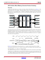
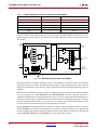
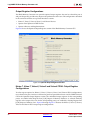
Overview
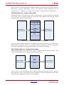
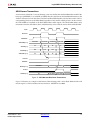
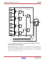
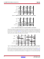
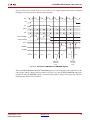
AXI4 Interface Block Memories are built on the Native Interface Block Memories (see Figure 1). Two
AXI4 interface styles are available - AXI4 and AXI4-Lite. The core can also be further classified as a
Memory Slave or as a Peripheral Slave. In addition to applications supported by the Native Interface
Block Memories, AXI4 Block Memories can also be used in AXI4 System Bus applications and Point-toPoint applications.
X-Ref Target - Figure 1
$;,0$67(5
:5,7(&+$11(/6
:5,7($''5(66
&+$11(/
:5,7('$7$
&+$11(/
:5,7(5(63
&+$11(/
$;,0$67(5
5($'&+$11(/6
$:9$/,'
$:5($'<
&+$11(/,1)2
:9$/,'
:5($'<
&+$11(/,1)2
$59$/,'
$55($'<
$;,
,17(5)$&(
:5,7()60
1$7,9(
%0*
&25(
$;,
,17(5)$&(
5($')60
%9$/,'
%5($'<
&+$11(/,1)2
&+$11(/,1)2
59$/,'
55($'<
&+$11(/,1)2
5($'$''5(66
&+$11(/
5($''$7$
&+$11(/
Figure 1: AXI4 Interface BMG Block Diagram
All communication in the AXI protocol is performed using five independent channels. Each of the five
independent channels consists of a set of information signals and uses a two-way VALID and READY
handshake mechanism. The information source uses the VALID signal to show when valid data or
control information is available on the channel. The information destination uses the READY signal to
show when it can accept the data.
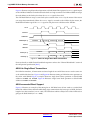
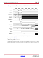
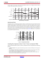
X-Ref Target - Figure 2
$&/.
9$/,'
,1)250$7,21
;;;
,1)2
;;;
,1)2
;;;
,1)2
;
5($'<
Figure 2: AXI4 Interface Handshake Timing Diagram
In Figure 2, the information source generates the VALID signal to indicate when data is available.
The destination generates the READY signal to indicate that it can accept the data, and transfer occurs
only when both the VALID and READY signals are high.
The AXI4 Block Memory Generator is an AXI4 endpoint Slave IP and can communicate with multiple
AXI4 Masters in an AXI4 System or with Standalone AXI4 Masters in point to point applications. The
core supports Simple Dual Port RAM configurations. Because AXI4 Block Memories are built using
Native interface Block Memories, they share many common features.
6
www.xilinx.com
DS512 March 1, 2011
Product Specification
LogiCORE IP Block Memory Generator v6.1
All Write operations are initiated on the Write Address Channel (AW) of the AXI bus. The AW channel
specifies the type of Write transaction and the corresponding address information. The Write Data
Channel (W) communicates all Write data for single or burst Write operations. The Write Response
Channel (B) is used as the handshaking or response to the Write operation.
On Read operations, the Read Address Channel (AR) communicates all address and control
information when the AXI master requests a Read transfer. When the Read data is available to send
back to the AXI master, the Read Data Channel (R) transfers the data and status of the Read operation
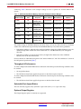
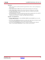
Applications
AXI4 Block Memories - Memory Slave Mode
AXI4 Block Memories in Memory Slave mode are optimized for Memory Mapped System Bus
implementations. The AXI4 Memory Slave Interface Type supports aligned, unaligned or narrow
transfers for incremental or wrap bursts.
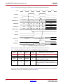
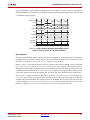
X-Ref Target - Figure 3
$;,/,7(%0*
0(025<6/$9(02'( $;,/,7(6/$9(
$;,/,7(6/$9(
$;,/LWH,QWHUFRQQHFW
3URFHVVRU3HULSKHUDO
,QWHUIDFH
Figure 3: AXI4 Memory Slave Application Diagram
Figure 3 shows an example application for the AXI4 Memory Slave Interface Type with an AXI4
Interconnect for Multi Master AXI4 applications. Minimum memory requirement for this configuration
is set to 4K bytes. Data widths supported by this configuration include 32, 64, 128 or 256 bits
AXI4-Lite Block Memories - Memory Slave Mode
AXI4-Lite Block Memories in Memory Slave mode are optimized for the AXI4-Lite interface. They can
be used in implementations requiring simple Control/Status Accesses. AXI4-Lite Memory Slave
Interface Type supports only single burst transactions.
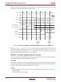
X-Ref Target - Figure 4
$;,%0*
0(025<6/$9(02'( $;,6/$9(
$;,,QWHUFRQQHFW
$;,0DVWHU
$;,0DVWHU
$;,0DVWHU
Figure 4: AXI4-Lite Memory Slave Application Diagram
DS512 March 1, 2011
Product Specification
www.xilinx.com
7
LogiCORE IP Block Memory Generator v6.1
Figure 4 shows an example application for AXI4-Lite Memory Slave Interface Type with an AXI4-Lite
Interconnect to manage Control/Status Accesses. The minimum memory requirement for this
configuration is set to 4K bytes. Data widths of 32 and 64 bits are supported by this configuration.
AXI4 Block Memories - Peripheral Slave Mode
AXI4 Block Memories in Peripheral Slave mode are optimized for a system or applications requiring
data transfers that are grouped together in packets. The AXI4 Peripheral Slave supports aligned
/unaligned addressing for incremental bursts.
X-Ref Target - Figure 5
%XIIHU$GGU&RQWURO1H[W3WU
%XIIHU$GGU&RQWURO1H[W3WU
%XIIHU
$;,0DVWHU
:ULWH&KDQQHOV
$;,%0*
3(5,3+(5$/6/$9(
02'(
$;,0DVWHU
5HDG&KDQQHOV
%XIIHU
Figure 5: AXI4 Peripheral Slave Application Diagram
Figure 5 shows an example application for the AXI4 Peripheral Slave Interface Type in a Point-to-point
buffered link list application. There is no minimum memory requirement set for this configuration.
Data widths supported by this configuration include 8, 16, 32, 64, 128 and 256 bits.
AXI4-Lite Block Memories - Peripheral Slave Mode
AXI4-Lite Block Memories in Peripheral Slave mode are optimized for the AXI4-Lite interface. They
can be used in implementations requiring single burst transactions.
X-Ref Target - Figure 74.2.4AXI4-Lite
6
8
Block Memories - Peripheral Slave Mode
'DWD&RQWURO
$;,/LWH0DVWHU
:ULWH&KDQQHOV
$;,/,7(
%0*
3(5,3+(5$/6/$9(
02'(
$;,/LWH0DVWHU 5HDG&KDQQHOV
Figure 8: AXI4-Lite Peripheral Slave Application Diagram
Figure 8 shows an example application for the AXI4-Lite Memory Slave Interface Type in a Point-topoint application. There is no minimum memory requirement set for this configuration. Data widths
supported by this configuration include 8, 16, 32 and 64 bits.
8
www.xilinx.com
DS512 March 1, 2011
Product Specification
LogiCORE IP Block Memory Generator v6.1
Supported Devices
Table 2: AXI4 BMG Supported FPGA Families and Sub-Families
FPGA Family
Sub-Family
Spartan-6
LX/LXT
Virtex-6
CXT/HXT/LXT/SXT
Virtex-7
Kintex-7
AXI4 BMG Core Channel Handshake Sequence
Figure 9 and Figure 10 illustrates an example handshake sequence for AXI4 BMG core. Figure 9
illustrates single burst Write operations to block RAM. By default the AWREADY signal is asserted on the
bus so that the address can be captured immediately during the clock cycle when both AWVALID and
AWREADY are asserted. (With the default set in this manner, there is no need to wait an extra clock cycle
AWREADY to be asserted first.) By default, the WREADY signal will be de-asserted. Upon detecting
AWVALID being asserted, the WREADY signal will be asserted (AXI4 BMG core has registered an AXI
Address and is ready to accept Data), and when WVALID is also asserted, writes will be performed to
the block RAM. If the write data channel (WVALID) is presented prior to the write address channel valid
(AWVALID) assertion, the write transactions will not be initiated until the write address channel has
valid information.
The AXI4 Block Memory core will assert BVALID for each transaction only after the last data transfer is
accepted. The core also will not wait for the master to assert BREADY before asserting BVALID.
X-Ref Target - Figure 9
$&/.
$:9$/,'
$:5($'<
$:$''5>@
;;;;;;;;
K
K
;;;;;;;;
:9$/,'
:5($'<
:'$7$ >@
;;;;;;;;
)$$$K
;;%$$K
;;;;;;;;
:675%>@
;;;;
E
E
;;;;
%9$/,'
%5($'<
%5(63>@
;;
E2.$<
;;
E2.$<
Figure 9: AXI4-Lite Single Burst Write Transactions
DS512 March 1, 2011
Product Specification
www.xilinx.com
9
LogiCORE IP Block Memory Generator v6.1
Figure 9 illustrates single burst Read operations to block RAM. The registered ARREADY signal output
on the AXI Read Address Channel interface defaults to a high assertion. The AXI Read FSM can accept
the read address in the clock cycle where the ARVALID signal is first valid.
The AXI Read FSM can accept a same clock cycle assertion of the RREADY by the master if the master
can accept data immediately. When the RREADY signal is asserted on the AXI bus by the master, the
Read FSM will either negate the RVALID signal or will place next valid data on the AXI Bus.
X-Ref Target - Figure 10
$&/.
$59$/,'
$55($'<
$5$''5>@
;;;;;;;;
K
;;;;;;;;
K
;;;;;;;;
59$/,'
55($'<
5'$7$ >@
;;;;;;;;
)$$$K
;;;;;;;;
$$K
;;;;;;;;
55(63>@
;;
E2.$<
;;
E2.$<
;;
Figure 10: AXI4 Lite Single Burst Read Transactions
For more details on AXI4 Channel handshake sequences refer to the “Channel Handshake” section of
the AXI protocol specification [Ref 1].
AXI4 Lite Single Burst Transactions
For AXI4 Lite interfaces, all transactions are burst length of one and all data accesses are the same size
as the width of the data bus. Figure 9 and Figure 10 illustrates timing of AXI 32-bit write operations to
the 32-bit wide BRAM. Figure 9 example illustrates single burst Write operations to block RAM
addresses 0x1000h and 0x1004h. Figure 10 illustrates single burst Read operations to block RAM
addresses 0x1000h and 0x1004h.
AXI4 Incremental Burst Support
Figure 11 illustrates an example of the timing for an AXI Write burst of four words to a 32-bit block
RAM. The address Write channel handshaking stage communicates the burst type as INCR, the burst
length of two data transfers (AWLEN = 01h). The Write burst utilizes all byte lanes of the AXI data bus
going to the block RAM (AWSIZE = 010b).
10
www.xilinx.com
DS512 March 1, 2011
Product Specification
LogiCORE IP Block Memory Generator v6.1
In compliance with AXI Protocol, the burst termination boundary for a transaction is determined by the
length specified in the AWLEN signal. The allowable burst sizes for INCR bursts are from 1 (00h) to 256
(FFh) data transfers.
X-Ref Target - Figure 11
$&/.
$:9$/,'
$:5($'<
;;;;;;;;
K
;;;;;;;;
K
;;;;;;;;
$:/(1>@
;;
K
;;;;;;;;
))K
;;
$:6,=(>@
;;;
E
;;;;;;;;
E
;;;
$:%8567>@
;;
E
;;;;;;;;
E
;;
$:$''5>@
:9$/,'
:5($'<
:'$7$ >@
;;;;;;;;
))))K
;;$$$K
$K
$$$$K
;;;;
E
E
E
E
E2.$<
;;
:/$67
:675%>@
%9$/,'
%5($'<
%5(63>@
;;
Figure 11: AXI4 Incremental Write Burst Transactions
Figure 12 illustrates the example timing for an AXI Read burst with block RAM managed by the Read
FSM. The memory Read burst starts at address 0x1000h of the block RAM. On the AXI Read Data
Channel, the Read FSM enables the AXI master/Interconnect to respond to the RVALID assertion when
RREADY is asserted in the same clock cycle. If the requesting AXI master/Interconnect throttles on
DS512 March 1, 2011
Product Specification
www.xilinx.com
11
LogiCORE IP Block Memory Generator v6.1
accepting the Read burst data (by negating RREADY), the Read FSM handles this by holding the data
pipeline until RREADY is asserted.
X-Ref Target - Figure 12
$&/.
$59$/,'
$55($'<
;;;;;;;;
K
K
;;;;;;;;
$5/(1>@
;;
K
))K
;;
$56,=(>@
;;;
E
E
;;;
$5%8567>@
;;
E
E
;;
$5$''5>@
59$/,'
55($'<
5'$7$ >@
;;;;;;;;
))))K
$$$K
$K
$$$$K
;;
E2.$<
E2.$<
E2.$<
E2.$<
5/$67
55(63>@
Figure 12: AXI4 Incremental Read Burst Transactions
AXI4 Wrap Burst Support
Cache line operations are implemented as WRAP burst types on AXI when presented to the block
RAM. The allowable burst sizes for WRAP bursts are 2, 4, 8, and 16. The AWBURST/ARBURST must be
set to “10” for the WRAP burst type.
WRAP bursts are handled by the address generator logic of the Write and Read FSM. The address seen
by the block RAM must increment to the address space boundary, and then wrap back around to the
beginning of the cache line address. For example, a processor issues a target word first cache line Read
request to address 0x04h. On a 32-bit block RAM, the address space boundary is 0xFFh. So, the block
12
www.xilinx.com
DS512 March 1, 2011
Product Specification
LogiCORE IP Block Memory Generator v6.1
RAM will see the following sequence of addresses for Read requests: 0x04h, 0x08h, 0x0Ch, 0x00h. Note
the wrap of the cache line address from 0xCh back to 0x00h at the end.
X-Ref Target - Figure 13
$&/.
$:9$/,'
$:5($'<
;;;;;;;;
K
;;;;;;;;
$:/(1>@
;;
K
;;
$:6,=(>@
;;;
E
;;;
$:%8567>@
;;
E
;;
$:$''5>@
:9$/,'
:5($'<
:'$7$ >@
;;;;;;;;
$$$$K
;;;;
E
$K
$K
''''K
;;;
E
E
;;;;
:/$67
:675%>@
E
%9$/,'
%5($'<
;;
%5(63>@
E2.$<
Figure 13: AXI4 Wrap Write Burst Transactions
Figure 13 illustrates the timing for AXI Wrap or cache line burst transactions. The address generated
and presented to the block RAM starts at the target word and wraps around once the address space
boundary is reached.
DS512 March 1, 2011
Product Specification
www.xilinx.com
13
LogiCORE IP Block Memory Generator v6.1
Figure 14 illustrates the timing on AXI WRAP or cache line burst Read transactions.
X-Ref Target - Figure 14
$&/.
$59$/,'
$55($'<
;;;;;;;;
K
;;;;;;;;
K
;;;;;;;;
$5/(1>@
;;
K
;;
)K
;;
$56,=(>@
;;;
E
;;;
E
;;;
$5%8567>@
;;
E
;;;
E
;;
$5$''5>@
59$/,'
55($'<
5'$7$ >@
;;;;;;;;
$$$$K
;;
E2.$<
$K
$K
''''K
E2.$<
E2.$<
5/$67
55(63>@
E2.$<
Figure 14: AXI4 Wrap Read Burst Transactions
Table 3 provides example address sequence to the block RAM for Wrap transactions.
Table 3: Example Address Sequence for AXI4 BMG Core Wrap Transactions
Memory
Width
Transfer
Size
Start
Address
Burst
Length
32-bits
32-bits
0x100Ch
2
0x100Ch(1), 0x1008h
32-bits
32-bits
0x1008h
4
0x1008h, 0x100Ch(1), 0x1000h, 0x1004h
64-bits
64-bits
0x1008h
8
0x1008h, 0x1010h, 0x1018h, 0x1020h, 0x1028h,
0x1030h, 0x1038h(1), 0x1000h
16
0x1008h, 0x100Ah, 0x100Ch, 0x100Eh, 0x1010,
0x1012, 0x1014, 0x1016h, 0x1018h, 0x101Ah,
0x101Ch, 0x101Eh(1), 0x1000h, 0x1002h, 0x1004h,
0x1006h
64-bits
1.
16-bits
0x1008h
AXI4 BMG Core Address Sequence
Calculated Wrap Boundary address.
For more details on AXI4 Wrap Burst Transactions and Wrap boundary calculations, refer to the Burst
Addressing section of the AXI protocol specification [Ref 1].
14
www.xilinx.com
DS512 March 1, 2011
Product Specification
LogiCORE IP Block Memory Generator v6.1
AXI4 Narrow Transactions
A narrow burst is defined as a master bursting a data size smaller than the block RAM data width. If the
burst type (AWBURST) is set to INCR or WRAP, then the valid data on the block RAM interface to the
AXI bus will rotate for each data beat. The Write and Read FSM handles each data beat on the AXI as a
corresponding data beat to the block RAM, regardless of the smaller valid byte lanes. In this scenario,
the AXI WSTRB is translated to the block RAM Write enable signals. The block RAM address only
increments when the full address (data) width boundary is met with the narrow Write to block RAM.
X-Ref Target - Figure 15
$&/.
$59$/,'
$55($'<
;;;;;;;;
K
;;;;;;;;
K
;;;;;;;;
$5/(1>@
;;
K
;;
K
;;
$56,=(>@
;;;
E
;;;
E
;;;
$5%8567>@
;;
E
;;
E
;;
$5$''5>@
59$/,'
55($'<
5'$7$ >@
;;;;;;;;
'';;;;K ;;;;''K
;;;;;;K
$;;;;;;K
E2.$<
E2.$<
E2.$<
5/$67
55(63>@
;;
E2.$<
Figure 15: AXI4 Narrow Write Burst Transactions
Figure 15 illustrates an example of AXI narrow Write bursting with a 32-bit block RAM and the AXI
master request is a half-word burst of four data beats. AWSIZE is set to 001b.
DS512 March 1, 2011
Product Specification
www.xilinx.com
15
LogiCORE IP Block Memory Generator v6.1
Figure 16 illustrates an example of AXI “narrow” Read bursting with a 32-bit block RAM and the AXI
master request is a half-word burst of 4 data beats. ARSIZE is set to 001b.
X-Ref Target - Figure 16
$&/.
$:9$/,'
$:5($'<
;;;;;;;;
K
;;;;;;;;
$:/(1>@
;;
K
;;
$:6,=(>@
;;;
E
;;;
$:%8567>@
;;
E
;;
$:$''5>@
:9$/,'
:5($'<
:'$7$ >@
;;;;;;;;
'';;;;K ;;;;''K '';;;;K
;;;;''K ;;;;;;;;
:/$67
:675%>@
;;;;
E
E
E
E
;;;;
%9$/,'
%5($'<
;;
%5(63>@
E2.$<
Figure 16: AXI4 Narrow Read Burst Transactions
For more details on AXI4 Narrow Transactions refer to the “Narrow transfers” section of the AXI
protocol specification [Ref 1].
AXI4 Unaligned Transactions
Unaligned burst transfers for example, occur when a 32-bit word burst size does not start on an address
boundary that matches a word memory location. The starting memory address is permitted to be
16
www.xilinx.com
DS512 March 1, 2011
Product Specification
LogiCORE IP Block Memory Generator v6.1
something other than 0x0h, 0x4h, 0x8h, etc. The example shown in Figure 17 illustrates an unaligned
word burst transaction of 4 data beats, which starts at address offset, 0x1002h.
X-Ref Target - Figure 17
'
'
'
'
'
'
'
'
'
'
'
'
'
'
'
'
Figure 17: AXI4 Unaligned Transactions
For more details on AXI4 Narrow Transactions refer to the “about unaligned transfers” section of the
AXI protocol specification [Ref 1].
Configurable Width and Depth
Table 4 provides supported Width and Depth for AXI4 Block Memory core.
Table 4: Supported Width and Depth
Operating
Mode
AXI4 Memory Slave
AXI4 Lite Memory Slave
AXI4 Peripheral Slave
AXI4 Lite Peripheral Slave
Supported Memory
Data Widths
Supported Minimum
Memory Depth
32,64,128, 256
Supports minimum 4kB address range:
Data Width Minimum Depth
32
1024
64
512
128
256
256
128
32,64
Supports minimum 4kB address range:
Data Width Minimum Depth
32
1024
64
512
8, 16, 32,64,128, 256
2
8, 16, 32,64,
2
For Peripheral Slave configurations, there is no minimum requirement for the number of address bits
used by Block Memory core. For Memory Slave configuration, AXI4 Block Memory slave has at least
sufficient address bits to fully decode a 4kB address range.
For Peripheral Slave and AXI4 Lite Memory Slave configurations, AXI4 Block Memory core is not
required to have low-order address bits to support decoding within the width of the system data bus
and assumes that such low-order address bits have a default value of all zeros. For AXI4 Memory Slave
configuration, AXI4 Block Memory core supports Narrow Transactions and performs low-order
address bits decoding. For more details, see AXI4 Interface Block Memory Addressing, page 17.
AXI4 Interface Block Memory Addressing
AXI4 Interface Block Memory cores support 32-bit byte addressing. There is no minimum requirement
for the number of address bits supplied by a master. Typically a master is expected to supply 32-bits of
DS512 March 1, 2011
Product Specification
www.xilinx.com
17
LogiCORE IP Block Memory Generator v6.1
addressing. Table 5 illustrates some example settings to create a specific size of block RAM in the
system.
Table 5: AXI4 Interface Block Memory Generator Example Address Ranges
Memory
Width x Depth
Memory
Size
Address Range
Required
Example
Base Address
Example
Max Address
Block RAM
Address
8 x 4096
4K
0x0000_0000
to 0x0000_0FFF
0xA000 0000
0xA000 0FFF
AXI_ADDR[11:0]
16 x 2048
4K
0x0000_0000
to 0x0000_0FFF
0xA000 0000
0xA000 0FFF
AXI_ADDR[11:1]
32 x 1024
4K
0x0000_0000
to 0x0000_0FFF
0xA000 0000
0xA000 0FFF
AXI_ADDR[11:2]
64 x 1024
8K
0x0000_0000
to 0x0000_1FFF
0x2400 0000
0x2400 1FFF
AXI_ADDR[12:3]
128 x 1024
16K
0x0000_0000
to 0x0000_3FFF
0x1F00 0000
0x1F00 3FFF
AXI_ADDR[13:4]
256 x 1024
32K
0x0000_0000
to 0x0000_7FFF
0x3000 0000
0x3000 7FFF
AXI_ADDR[14:5]
The Address Range of AXI Block Memory core must always start at zero. If the master has a different
address bus width than that provided by the AXI4 Block Memory Core, follow these guidelines:
•
If the Master address is wider than the configured Address Range for AXI Block Memory core, the
additional high-order address bits can be connected as is. AXI Block Memory core will ignore
these bits.
•
If the Master address is narrower than 32-bits, the high-order address bits of the AXI Block
Memory core can be left unconnected.
For more details on AXI4 Addressing refer to the “Master Addresses” and “Slave Addresses” section of
the AXI protocol specification [Ref 1].
Throughput & Performance
To achieve 100 percent block RAM interface utilization of the Write port the following conditions must
be satisfied.
•
No single Write bursts.
•
The AXI Master should not apply back pressure on the Write response channel
To achieve 100 percent block RAM interface utilization of the Read port the following conditions must
be satisfied.
•
The AXI Master should not apply back pressure on the Read data channel
Selectable Port Aspect Ratios
The core currently supports only symmetric aspect ratios (that is, a 1:1 aspect ratio only).
Optional Output Register
The Output Register option is currently not supported.
18
www.xilinx.com
DS512 March 1, 2011
Product Specification
LogiCORE IP Block Memory Generator v6.1
Optional Pipeline Stages
Pipeline stages are currently not supported.
Memory Initialization Capability
The memory contents can be optionally initialized using a memory coefficient (COE) file or by
specifying a default data value. A COE file can define the initial contents of each individual memory
location, while the default data value option defines the initial content for all locations.
Simulation Models
The Block Memory Generator core provides behavioral and structural simulation models in VHDL and
Verilog to give the user the option to perform either simple or precise modeling of memory behaviors,
respectively.
Block Memory Generator Functional Description
The Block Memory Generator is used to build custom memory modules from block RAM primitives in
Xilinx FPGAs. The core implements an optimal memory by arranging block RAM primitives based on
user selections, automating the process of primitive instantiation and concatenation. Using the CORE
Generator Graphical User Interface (GUI), users can configure the core and rapidly generate a highly
optimized custom memory solution.
Memory Type
The Block Memory Generator creates five memory types: Single-port RAM, Simple Dual-port RAM,
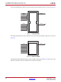
True Dual-port RAM, Single-port ROM, and Dual-port ROM. Figure 18 through Figure 22 illustrate the
signals available for each type. Optional pins are displayed in italics.
For each configuration, optimizations are made within the core to minimize the total resources used.
For example, a Simple Dual-port RAM with symmetric ports can utilize the special Simple Dual-port
RAM primitive in Virtex-5 devices, which can save as much as fifty percent of the block RAM resources
for memories 512 words deep or fewer. The Single-port ROM allows Read access to the memory space
through a single port, as illustrated in Figure 18.
X-Ref Target - Figure 18
Single-Port ROM
ADDRA
DOUTA
ENA
RSTA
REGCEA
CLKA
Figure 18: Single-port ROM
DS512 March 1, 2011
Product Specification
www.xilinx.com
19
LogiCORE IP Block Memory Generator v6.1
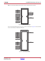
The Dual-port ROM allows Read access to the memory space through two ports, as shown in Figure 19.
X-Ref Target - Figure 19
Dual-Port ROM
ADDRA
DOUTA
ENA
RSTA
REGCEA
CLKA
ADDRB
DOUTB
ENB
RSTB
REGCEB
CLKB
Figure 19: Dual-port ROM
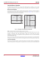
The Single-port RAM allows Read and Write access to the memory through a single port, as shown in
Figure 20.
X-Ref Target - Figure 20
Single-Port RAM
DINA
DOUTA
ADDRA
WEA
ENA
RSTA
REGCEA
CLKA
Figure 20: Single-port RAM
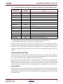
The Simple Dual-port RAM provides two ports, A and B, as illustrated in Figure 21. Write access to the
memory is allowed via port A, and Read access is allowed via port B.
20
www.xilinx.com
DS512 March 1, 2011
Product Specification
LogiCORE IP Block Memory Generator v6.1
Note: For Virtex family architectures, Read access is via port A and Write access is via port B.
X-Ref Target - Figure 21
Simple Dual-Port RAM
DINA
ADDRA
WEA
SBITERR
ENA
DBITERR
CLKA
RDADDRECC
INJECTSBITERR
INJECTDBITERR
ADDRB
DOUTB
ENB
RSTB
REGCEB
CLKB
Figure 21: Simple Dual-port RAM
The True Dual-port RAM provides two ports, A and B, as illustrated in Figure 22. Read and Write
accesses to the memory are allowed on either port.
X-Ref Target - Figure 22
True Dual-Port RAM
DINA
DOUTA
ADDRA
WEA
ENA
RSTA
REGCEA
CLKA
DINB
DOUTB
ADDRB
WEB
ENB
RSTB
REGCEB
CLKB
Figure 22: True Dual-port RAM
DS512 March 1, 2011
Product Specification
www.xilinx.com
21
LogiCORE IP Block Memory Generator v6.1
Selectable Memory Algorithm
The Block Memory Generator core arranges block RAM primitives according to one of three
algorithms: the minimum area algorithm, the low power algorithm and the fixed primitive algorithm.
Minimum Area Algorithm
The minimum area algorithm provides a highly optimized solution, resulting in a minimum number of
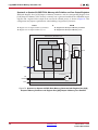
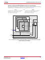
block RAM primitives used, while reducing output multiplexing. Figure 23 shows two examples of
memories built using the minimum area algorithm.
X-Ref Target - Figure 23
3kx16 memory
2kx9
5kx17 memory
2kx9
2kx9
4kx4
4kx4
1kx18
2kx9
1kx18
Figure 23: Examples of the Minimum Area Algorithm
Note: In Spartan-6 devices, two 9K block RAMs are used for one 1Kx18.
In the first example, a 3kx16 memory is implemented using three block RAMs. While it may have been
possible to concatenate three 1kx18 block RAMs in depth, this would require more output
multiplexing. The minimum area algorithm maximizes performance in this way while maintaining
minimum block RAM usage.
In the second example, a 5kx17 memory, further demonstrates how the algorithm can pack block RAMs
efficiently to use the fewest resources while maximizing performance by reducing output multiplexing.
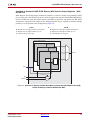
Low Power Algorithm
The low power algorithm provides a solution that minimizes the number of primitives enabled during
a Read or Write operation. This algorithm is not optimized for area and may use more block RAMs and
22
www.xilinx.com
DS512 March 1, 2011
Product Specification
LogiCORE IP Block Memory Generator v6.1
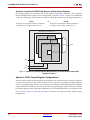
multiplexers than the minimum area algorithm. Figure 24 shows two examples of memories built
using the low power algorithm.
X-Ref Target - Figure 24
3kx16 Memory
5kx17 Memory
1kx18
1kx18
1kx18
1kx18
1kx18
1kx18
1kx18
1kx18
Figure 24: Examples of the Low Power Algorithm
Note: In Spartan-6 devices, two 9K block RAMs are used for one 1Kx18.
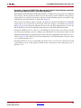
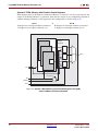
Fixed Primitive Algorithm
The fixed primitive algorithm allows the user to select a single block RAM primitive type. The core will
build the memory by concatenating this single primitive type in width and depth. It is useful in
systems that require a fixed primitive type. Figure 25 depicts two 3kx16 memories, one built using the
2kx9 primitive type, the other built using the 4kx4 primitive type.
X-Ref Target - Figure 25
3kx16 memory
2kx9
3kx16 memory
2kx9
4kx4
2kx9
4kx4
4kx4
4kx4
2kx9
Figure 25: Examples of the Fixed Primitive Algorithm
Note that both implementations use four block RAMs, and that some of the resources utilized extend
beyond the usable memory space. It is up to the user to decide which primitive type is best for their
application.
The fixed primitive algorithm provides a choice of 16kx1, 8kx2, 4kx4, 2kx9, 1kx18, 512x36, 256x72 and
256x36 primitives. The primitive type selected is used to guide the construction of the total user
memory space. Whenever possible, optimizations are made automatically that use deeper embedded
DS512 March 1, 2011
Product Specification
www.xilinx.com
23
LogiCORE IP Block Memory Generator v6.1
memory structures to enhance performance. Table 6 shows the primitives used to construct a memory
given the specified architecture and primitive selection.
Table 6: Memory Primitives Used Based on Architecture (Supported in Native BMG)
Architecture
24
Primitive
Selection
Primitives
Used
Spartan-6 FPGA
16kx1
8kx1,16kx1
Spartan-6 FPGA
8kx2
4kx2,8kx2
Spartan-6 FPGA
4kx4
2kx4,4kx4
Spartan-6 FPGA
2kx9
1kx9,2kx9
Spartan-6 FPGA
1kx18
512x18,1kx18
Spartan-6 FPGA
512x36
512x36
Spartan-6 FPGA
256x72
256x72 (SP RAM/ROM configurations only)
Spartan-6 FPGA
256x36
256x36 (SP RAM/ROM and SDP configurations only) (2)
Spartan-3 (1)FPGA
16kx1
16kx1
Spartan-3 (1)
FPGA
8kx2
8kx2
Spartan-3 (1)
FPGA
4kx4
4kx4
Spartan-3 (1)
FPGA
2kx9
2kx9
Spartan-3 (1)
FPGA
1kx18
1kx18
Spartan-3 (1)
FPGA
512x36
512x36
Spartan-3 (1)
FPGA
256x72
256x72 (Single Port configurations only)
Kintex-7 FPGA
16kx1
64x1, 32kx1, 16kx1
Kintex-7 FPGA
8kx2
16kx2, 8kx2
Kintex-7 FPGA
4kx4
4kx4, 8kx4
Kintex-7 FPGA
2kx9
2kx9, 4kx9
Kintex-7 FPGA
1kx18
1kx18, 2kx18
Kintex-7 FPGA
512x36
512x36 (SP RAM/ROM and SDP configurations only), 1kx36
Kintex-7 FPGA
256x72
512x72 (SP RAM/ROM and SDP configurations only)
Virtex-7 FPGA
16kx1
64x1, 32kx1, 16kx1
Virtex-7 FPGA
8kx2
16kx2, 8kx2
Virtex-7 FPGA
4kx4
4kx4, 8kx4
Virtex-7 FPGA
2kx9
2kx9, 4kx9
Virtex-7 FPGA
1kx18
1kx18, 2kx18
Virtex-7 FPGA
512x36
512x36 (SP RAM/ROM and SDP configurations only), 1kx36
Virtex-7 FPGA
256x72
512x72 (SP RAM/ROM and SDP configurations only)
Virtex-6 FPGA
16kx1
64x1, 32kx1, 16kx1
Virtex-6 FPGA
8kx2
16kx2, 8kx2
Virtex-6 FPGA
4kx4
4kx4, 8kx4
Virtex-6 FPGA
2kx9
2kx9, 4kx9
Virtex-6 FPGA
1kx18
1kx18, 2kx18
Virtex-6 FPGA
512x36
512x36 (SP RAM/ROM and SDP configurations only), 1kx36 (2)
www.xilinx.com
DS512 March 1, 2011
Product Specification
LogiCORE IP Block Memory Generator v6.1
Table 6: Memory Primitives Used Based on Architecture (Supported in Native BMG) (Cont’d)
Architecture
Primitive
Selection
Primitives
Used
512x72 (SP RAM/ROM and SDP configurations only)(2)
Virtex-6 FPGA
256x72
Virtex-5 FPGA
16kx1
64kx1, 32kx1, 16kx1
Virtex-5 FPGA
8kx2
16kx2, 8kx2
Virtex-5 FPGA
4kx4
8kx4, 4kx4
Virtex-5 FPGA
2kx9
4kx9, 2kx9
Virtex-5 FPGA
1kx18
2kx18, 1kx18
Virtex-5 FPGA
512x36
1kx36
Virtex-5 FPGA
256x72
512x72 (Single and Simple Dual-port RAMs and Single Port
ROMs only)
Virtex-4 FPGA
16kx1
32kx1, 16kx1
Virtex-4 FPGA
8kx2
8kx2
Virtex-4 FPGA
4kx4
4kx4
Virtex-4 FPGA
2kx9
2kx9
Virtex-4 FPGA
1kx18
1kx18
Virtex-4 FPGA
512x36
512x36
Virtex-4 FPGA
256x72
256x72 (Single Port configurations only)
Notes:
1.
2.
Spartan-3 FPGAs and its derivatives, including Spartan-3E and Spartan-3A/3A DSP devices.
Refer to Additional memory collision restrictions in Collision Behavior, page 30.
When using data-width aspect ratios, the primitive type dimensions are chosen with respect to the A
port Write width. Note that primitive selection may limit port aspect ratios as described in Aspect Ratio
Limitations, page 29. When using the byte Write feature in Kintex-7, Virtex-7, Virtex-6, Virtex-5, Virtex4, Spartan-6, and Spartan-3A/3A DSP devices, only the 2kx9, 1kx18, and 512kx36 primitive choices are
available.
Selectable Width and Depth
The Block Memory Generator generates memories with widths from 1 to 1152 bits, and with depths of
two or more words. The memory is built by concatenating block RAM primitives, and total memory
size is limited only by the number of block RAMs on the target device.
Write operations to out-of-range addresses are guaranteed not to corrupt data in the memory, while
Read operations to out-of-range addresses will return invalid data. Note that the set/reset function
should not be asserted while accessing an out-of-range address as this also results in invalid data on the
output in the present or following clock cycles depending upon the output register stages of the core.
Operating Mode
The operating mode for each port determines the relationship between the Write and Read interfaces
for that port. Port A and port B can be configured independently with any one of three Write modes:
Write First Mode, Read First Mode, or No Change Mode. These operating modes are described in the
sections that follow.
DS512 March 1, 2011
Product Specification
www.xilinx.com
25
LogiCORE IP Block Memory Generator v6.1
The operating modes have an effect on the relationship between the A and B ports when the A and B
port addresses have a collision. For detailed information about collision behavior, see Collision
Behavior, page 30. For more information about operating modes, see the block RAM section of the user
guide specific to the device family.
•
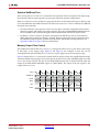
Write First Mode: In WRITE_FIRST mode, the input data is simultaneously written into memory
and driven on the data output, as shown in Figure 26. This transparent mode offers the flexibility
of using the data output bus during a Write operation on the same port.
X-Ref Target - Figure 26
CLKA
WEA
DINA[15:0]
ADDRA
DOUTA[15:0]
1111
2222
bb
cc
aa
0000
MEM(aa)
1111
dd
2222
MEM(dd)
ENA
DISABLED
WRITE
MEM(bb)=
1111
READ
WRITE
MEM(cc)=
2222
READ
Figure 26: Write First Mode Example
Note: The WRITE_FIRST operation is affected by the optional byte-Write feature in Kintex-7, Virtex-7, Virtex6, Virtex-5, Virtex-4, Spartan-6 and Spartan-3A/3A DSP devices. It is also affected by the optional Read-toWrite aspect ratio feature in Kintex-7, Virtex-7, Virtex-6, Virtex-5 and Virtex-4 devices. For detailed information,
see Write First Mode Considerations, page 30.
•
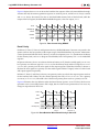
Read First Mode: In READ_FIRST mode, data previously stored at the Write address appears on
the data output, while the input data is being stored in memory. This Read-before-Write behavior
is illustrated in Figure 27.
X-Ref Target - Figure 27
CLKA
WEA
DINA[15:0]
ADDRA
DOUTA[15:0]
1111
2222
bb
cc
aa
0000
MEM(aa)
old MEM(bb)
dd
old MEM(cc)
MEM(dd)
ENA
DISABLED
READ
WRITE
MEM(bb)=
1111
WRITE
MEM(cc)=
2222
READ
Figure 27: Read First Mode Example
26
www.xilinx.com
DS512 March 1, 2011
Product Specification
LogiCORE IP Block Memory Generator v6.1
•
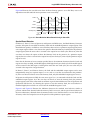
No Change Mode: In NO_CHANGE mode, the output latches remain unchanged during a Write
operation. As shown in Figure 28, the data output is still the previous Read data and is unaffected
by a Write operation on the same port.
X-Ref Target - Figure 28
CLKA
WEA
DINA[15:0]
ADDRA
1111
2222
bb
cc
aa
DOUTA[15:0]
0000
dd
MEM(aa)
MEM(dd)
ENA
DISABLED
WRITE
MEM(bb)=
1111
READ
WRITE
MEM(cc)=
2222
READ
Figure 28: No Change Mode Example
Data Width Aspect Ratios
The Block Memory Generator supports data width aspect ratios. This allows the port A data width to
be different than the port B data width, as described in Port Aspect Ratios in the following section. In
Kintex-7, Virtex-7, Virtex-6, Virtex-5 and Virtex-4 FPGA-based memories, all four data buses (DINA,
DOUTA, DINB, and DOUTB) can have different widths, as described in Kintex-7, Virtex-7, Virtex-6,
Virtex-5 and Virtex-4 Read-to-Write Aspect Ratios, page 28.
The limitations of the data width aspect ratio feature (some of which are imposed by other optional
features) are described in Aspect Ratio Limitations, page 29. The CORE Generator GUI ensures only
valid aspect ratios are selected.
Port Aspect Ratios
The Block Memory Generator supports port aspect ratios of 1:32, 1:16, 1:8, 1:4, 1:2, 1:1, 2:1, 4:1, 8:1, 16:1,
and 32:1. The port A data width can be up to 32 times larger than the port B data width, or vice versa.
The smaller data words are arranged in little-endian format, as illustrated in Figure 29.
Port Aspect Ratio Example
Consider a True Dual-port RAM of 32x2048, which is the A port width and depth. From the perspective
of an 8-bit B port, the depth would be 8192. The ADDRA bus is 11 bits, while the ADDRB bus is 13 bits.
The data is stored little-endian, as shown in Figure 29. Note that An is the data word at address n, with
respect to the A port. Bn is the data word at address n with respect to the B port. A0 is comprised of B3,
B2, B1, and B0.
X-Ref Target - Figure 29
31
A0 =
A1 =
0
7 .. 0
7 .. 0
7 .. 0
7 .. 0
B3
B2
B1
B0
7 .. 0
7 .. 0
7 .. 0
7 .. 0
B7
B6
B5
B4
.
.
.
Figure 29: Port Aspect Ratio Example Memory Map
DS512 March 1, 2011
Product Specification
www.xilinx.com
27
LogiCORE IP Block Memory Generator v6.1
Kintex-7, Virtex-7, Virtex-6, Virtex-5 and Virtex-4 Read-to-Write Aspect Ratios
When implementing RAMs targeting Kintex-7, Virtex-7, Virtex-6, Virtex-5 and Virtex-4 FPGAs, the
Block Memory Generator allows Read and Write aspect ratios on either port. On each port A and port
B, the Read to Write data width ratio of that port can be 1:32, 1:16, 1:8, 1:4, 1:2, 1:1, 2:1, 4:1, 8:1, 16:1, or
32:1.
Because the Read and Write interfaces of each port can differ, it is possible for all four data buses (DINA,
DOUTA, DINB, and DOUTB) of True Dual-port RAMs to have a different width. For Single-port RAMs,
DINA and DOUTA widths can be independent. The maximum ratio between any two data buses is 32:1.
The widest data bus can be no larger than 1152 bits.
If the Read and Write data widths on a port are different, the memory depth is different with respect to
Read and Write accesses. For example, if the Read interface of port A is twice as wide as the Write
interface, then it is also half as deep. The ratio of the widths is always the inverse of the ratio of the
depths. Because a single address bus is used for both the Write and Read interface of a port, the address
bus must be large enough to address the deeper of the two depths. For the shallower interface, the least
significant bits of the address bus are ignored. The data words are arranged in little-endian format, as
illustrated in Figure 30.
Kintex-7, Virtex-7, Virtex-6, Virtex-5 and Virtex-4 Read-to-Write Aspect Ratio Example
Consider a True Dual-port RAM of 64x512, which is the port A Write width and depth. Table 7 defines
the four data-port widths and their respective depths for this example.
Table 7: Read-to-Write Aspect Ratio Example Ports
Interface
Data Width
Memory Depth
Port A Write
64
512
Port A Read
16
2048
Port B Write
256
128
Port B Read
32
1024
The ADDRA width is determined by the larger of the A port depths (2048). For this reason, ADDRA is 11
bits wide. On port A, Read operations utilize the entire ADDRA bus, while Write operations ignore the
least significant 2 bits.
In the same way, the ADDRB width is determined by the larger of the B port depths (1024). For this
reason, ADDRB is 10 bits wide. On port B, Read operations utilize the entire ADDRB bus, while Write
operations ignore the least significant 3 bits.
The memory map in Figure 30 shows how port B Write words are related to port A Write words, in a
little-endian arrangement. Note that AWn is the Write data word at address n with respect to port A,
while BWn is the Write data word at address n with respect to port B.
X-Ref Target - Figure 30
255
0
BW 0 =
AW 3
AW 2
AW 1
AW 0
BW 1 =
AW 7
AW 6
AW 5
AW 4
.
.
.
Figure 30: Read-to-Write Aspect Ratio Example Memory Map
28
www.xilinx.com
DS512 March 1, 2011
Product Specification
LogiCORE IP Block Memory Generator v6.1
BW0 is made up of AW3, AW2, AW1, and AW0. In the same way, BR0 is made up of AR1 and AR0, and
AW0 is made up of BR1 and BR0. In the example above, the largest data width ratio is port B Write
words (256 bits) to port A Read words (16 bits); this ratio is 16:1.
Aspect Ratio Limitations
In general, no port data width can be wider than 1152 bits, and no two data widths can have a ratio
greater than 32:1. However, the following optional features further limit data width aspect ratios:
•
Byte-writes. When using byte-writes, no two data widths can have a ratio greater than 4:1.
•
Fixed primitive algorithm. When using the fixed primitive algorithm with an N-bit wide
primitive, aspect ratios are limited to 32:N and 1:N from the port A Write width. For example,
using the 4kx4 primitive type, the other ports may be no more than 8 times (32:4) larger than port
A Write width and no less than 4 times (1:4) smaller.
Byte-Writes
The Block Memory Generator provides byte-Write support in Kintex-7, Virtex-7, Virtex-6, Virtex-5,
Virtex-4, Spartan-6, and Spartan-3A/3A DSP devices. Byte-writes are available using either 8-bit or 9bit byte sizes. When using an 8-bit byte size, no parity bits are used and the memory width is restricted
to multiples of 8 bits. When using a 9-bit byte size, each byte includes a parity bit, and the memory
width is restricted to multiples of 9 bits.
When byte-writes are enabled, the WE[A|B] (WEA or WEB) bus is N bits wide, where N is the number
of bytes in DIN[A|B]. The most significant bit in the Write enable bus corresponds to the most
significant byte in the input word. Bytes will be stored in memory only if the corresponding bit in the
Write enable bus is asserted during the Write operation.
When 8-bit bytes are selected, the DIN and DOUT data buses are constructed from 8-bit bytes, with no
parity. When 9-bit bytes are selected, the DIN and DOUT data buses are constructed from 9-bit bytes,
with the 9th bit of each byte in the data word serving as a parity bit for that byte.
The byte-Write feature may be used in conjunction with the data width aspect ratios, which may limit
the choice of data widths as described in Data Width Aspect Ratios, page 27. However, it may not be
used with the NO_CHANGE operating mode. This is because if a memory configuration uses multiple
primitives in width, and only one primitive is being written to (using partial byte writes), then the
NO_CHANGE mode only applies to that single primitive. The NO_CHANGE mode does not apply to
the other primitives that are not being written to, so these primitives can still be read. The byte-Write
feature also affects the operation of WRITE_FIRST mode, as described in Write First Mode
Considerations, page 30.
DS512 March 1, 2011
Product Specification
www.xilinx.com
29
LogiCORE IP Block Memory Generator v6.1
Byte-Write Example
Consider a Single-port RAM with a data width of 24 bits, or 3 bytes with byte size of 8 bits. The Write
enable bus, WEA, consists of 3 bits. Figure 31 illustrates the use of byte-writes, and shows the contents
of the RAM at address 0. Assume all memory locations are initialized to 0.
X-Ref Target - Figure 31
CLKA
WEA[2:0]
b011
b010
b101
ADDRA[15:0]
DINA[23:0]
b000
b110
b010
66 55 44
33 22 11
00 FF 00
0000
FF EE DD
RAM Contents
CC BB AA
00 EE DD
99 88 77
00 BB DD
99 BB 77
33 22 77
33 FF 77
Figure 31: Byte-Write Example
Write First Mode Considerations
When performing a Write operation in WRITE_FIRST mode, the concurrent Read operation shows the
newly written data on the output of the core. However, when using the byte-Write feature in Kintex-7,
Virtex-7, Virtex-6, Virtex-5, Virtex-4, Spartan-6, and Spartan-3A/3A DSP devices or the Read-to-Write
aspect ratio feature in Kintex-7, Virtex-7, Virtex-6, Virtex-5 and Virtex-4 devices, the output of the
memory cannot be guaranteed.
Collision Behavior
The Block Memory Generator core supports Dual-port RAM implementations. Each port is equivalent
and independent, yet they access the same memory space. In such an arrangement, is it possible to have
data collisions. The ramifications of this behavior are described for both asynchronous and
synchronous clocks below.
Collisions and Asynchronous Clocks: General Guidelines
Using asynchronous clocks, when one port writes data to a memory location, the other port must not
Read or Write that location for a specified amount of time. This clock-to-clock setup time is defined in
the device data sheet, along with other block RAM switching characteristics.
Collisions and Synchronous Clocks: General Guidelines
Synchronous clocks cause a number of special case collision scenarios, described below.
•
30
Synchronous Write-Write Collisions. A Write-Write collision occurs if both ports attempt to Write
to the same location in memory. The resulting contents of the memory location are unknown. Note
that Write-Write collisions affect memory content, as opposed to Write-Read collisions which only
affect data output.
www.xilinx.com
DS512 March 1, 2011
Product Specification
LogiCORE IP Block Memory Generator v6.1
•
Using Byte-Writes. When using byte-writes, memory contents are not corrupted when separate
bytes are written in the same data word. RAM contents are corrupted only when both ports
attempt to Write the same byte. Figure 32 illustrates this case. Assume ADDRA = ADDRB = 0.
X-Ref Target - Figure 32
CLKA
WEA[3:0]
b1100
b0101
b1110
WEB[3:0]
b0011
b1010
b0011
b0110
b1111
DINA[31:0]
7654 FFFF
AAAA AAAA
7777 7777
AAAA AAAA
1111 1111
DINB[31:0]
FFFF 3210
BBBB BBBB
0000 0000
BBBB BBBB
2222 2222
RAM Contents
7654 3210
BBAA BBAA
b1111
7777 XX00
AAXX XXAA
XXXX XXXX
Figure 32: Write-Write Collision Example
•
Synchronous Write-Read Collisions. A synchronous Write-Read collision may occur if a port
attempts to Write a memory location and the other port reads the same location. While memory
contents are not corrupted in Write-Read collisions, the validity of the output data depends on the
Write port operating mode.
•
If the Write port is in READ_FIRST mode, the other port can reliably read the old memory
contents.
•
If the Write port is in WRITE_FIRST or NO_CHANGE mode, data on the output of the Read
port is invalid.
•
In the case of byte-writes, only bytes which are updated will be invalid on the Read port
output.
Figure 33 illustrates Write-Read collisions and the effects of byte-writes. DOUTB is shown for when port
A is in WRITE_FIRST mode and READ_FIRST mode. Assume ADDRA = ADDRB = 0, port B is always
reading, and all memory locations are initialized to 0. The RAM contents are never corrupted in WriteRead collisions.
X-Ref Target - Figure 33
CLKA
WEA[3:0]
b0000
b0101
DINA[31:0]
AAAA AAAA
DOUTBARF
0000 0000
DOUTBAWF
0000 0000
RAM Contents
0000 0000
b0000
b1100
b1111
3322 1100
1111 1111
00AA 00AA
00XX 00XX
00AA 00AA
00AA 00AA
XXXX 00AA
b0000
3322 00AA
1111 1111
XXXX XXXX
1111 1111
3322 00AA
1111 1111
Figure 33: Write-Read Collision Example
Collisions and Simple Dual-port RAM
For Simple Dual-port RAM, the operating modes are not selectable, but are automatically set to either
READ_FIRST or WRITE_FIRST depending on the target device family and clocking configuration
(synchronous or asynchronous). The Simple Dual-port RAM is like a true dual-port RAM where only
the Write interface of the A port and the Read interface of B port are connected. The operating modes
DS512 March 1, 2011
Product Specification
www.xilinx.com
31
LogiCORE IP Block Memory Generator v6.1
define the Write-to-Read relationship of the A or B ports, and only impact the relationship between A
and B ports during an address collision.
For Synchronous Clocking and during a collision, the Write mode of port A can be configured so that a
Read operation on port B either produces data (acting like READ_FIRST), or produces undefined data
(Xs). For this reason, the core is hard-coded to produce READ_FIRST-like behavior when configured as
a Simple Dual-port RAM. For detailed information about this behavior, see Collision Behavior, page 30.
Exceptions: For Kintex-7, Virtex-7, Virtex-6, and Spartan-6 devices, the operating mode (READ_FIRST
or WRITE_FIRST respectively) is determined by whether the clocking mode selection is Synchronous
(Common Clock) or Asynchronous. See Clocking Options, page 65 for more details.
Additional Memory Collision Restrictions: Address Space Overlap
Kintex-7, Virtex-7, Virtex-6 and Spartan-6 FPGA block RAM memories have additional collision
restrictions in the following configurations:
•
When configured as True Dual Port (TDP)
•
When CLKA (port A) and CLKB (port B) are Asynchronous
•
In applications that perform a simultaneous Read and Write
•
When either port A, port B, or both ports are configured with Write Mode configured as
READ_FIRST
When using TDP Memory with Write Mode = READ_FIRST (TDP-RF mode) in conjunction with
asynchronous clocking, see the “Conflict Avoidance” section of the 7 Series FPGAs Memory Resources
User Guide (UG473), the Virtex-6 FPGA Memory Resources User Guide (UG363) or the Spartan-6 FPGA
Block RAM Resources User Guide (UG383).
For Kintex-7, Virtex-7, Virtex-6 and Spartan-6 devices using the TDP-RF mode, the Address Space
Overlap issue must be considered.
Optional Output Registers
The Block Memory Generator allows optional output registers, which may improve the performance of
the core. The user may choose to include register stages at two places: at the output of the block RAM
primitives and at the output of the core.
Registers at the output of the block RAM primitives reduce the impact of the clock-to-out delay of the
primitives. Registers at the output of the core isolate the delay through the output multiplexers,
improving the clock-to-out delay of the Block Memory Generator core. Each of the two optional register
stages can be chosen for port A and port B separately. Note that each optional register stage used adds
an additional clock cycle of latency to the Read operation.
32
www.xilinx.com
DS512 March 1, 2011
Product Specification
LogiCORE IP Block Memory Generator v6.1
Figure 34 shows a memory configuration with registers at the output of the memory primitives and at
the output of the core for one of the ports.
X-Ref Target - Figure 34
Block Memory Generator Core
Block RAM Primitives
Primitive
Output
Registers
Block RAM
Block RAM
D
Q
Core
Output
Registers
CE
Latches
Block RAM
Latches
D
Q
MUX
D
Q
DOUT
CE
CE
S*
Latches
D
Q
CE
CLK
Use REGCE Pin
EN
REGCE
FALSE
TRUE
RST
S* : The synchronous reset (S) of the flop is gated by CE
Figure 34: Spartan-3 Block Memory: Register Port [A|B] Outputs of Memory Primitives
and Memory Core Options Enabled
DS512 March 1, 2011
Product Specification
www.xilinx.com
33
LogiCORE IP Block Memory Generator v6.1
For Kintex-7, Virtex-7, Virtex-6, Virtex-5, Virtex-4, Spartan-6, and Spartan-3A DSP FPGAs, the Register
Port [A|B] Output of Memory Primitives option may be implemented using the embedded block RAM
registers, requiring no further FPGA resources. All other register stages are implemented in FPGA
fabric. Figure 35 shows an example of a Kintex-7, Virtex-7, Virtex-6, Virtex-5 or Virtex-4 FPGA-based
memory that has been configured using both output register stages for one of the ports.
X-Ref Target - Figure 35
Block Memory Generator Core
Block RAM Primitives
Embedded
Output Registers
Core
Output
Registers
Embedded
Output Registers
Latches
Latches
Embedded
Output Registers
Latches
CE
Latches
Latches
CE
Block RAM
MUX
D
Q
DOUT
CE
R*
SSR*
Block RAM
SSR*
Block RAM
D
Q
CE
CLK
Use REGCE Pin
EN
REGCE
FALSE
TRUE
RST
R* : The reset (R) of the flop is gated by CE
Figure 35: Kintex-7, Virtex-7, Virtex-6, Virtex-5, and Virtex-4 Block Memory with Register Port
[A|B] Output of Memory Primitives and Register Port [A|B] Output of
Memory Core Options Enabled
When using the Synchronous Reset Input (RST), the behavior of the embedded output registers in the
Spartan-3A DSP FPGA differs slightly from the configuration shown in Figure 35. By default, the Block
Memory Generator builds the memory output register in the FPGA fabric to maintain functionality
compatibility with Kintex-7, Virtex-7, Virtex-6, Virtex-5 and Virtex-4 FPGA configurations. To force the
core to use the embedded output registers in Spartan-6 and Spartan-3A DSP devices, the Reset
Behavior options are provided. For a complete description of the supported output options, see Output
Register Configurations, page 96.
Optional Pipeline Stages
The Block Memory Generator core allows optional pipeline stages within the MUX, which may
improve core performance. Users can add up to three pipeline stages within the MUX, excluding the
registers at the output of the core. This optional pipeline stages option is available only when the
registers at the output of the memory core are enabled and when the constructed memory has more
than one primitive in depth, so that a MUX is needed on the output.
34
www.xilinx.com
DS512 March 1, 2011
Product Specification
LogiCORE IP Block Memory Generator v6.1
The pipeline stages are common for port A and port B and can be a value of 1, 2, or 3 if the Register
Output of Memory Core option is selected in the GUI for both port A and port B. Note that each
pipeline stage adds an additional clock cycle of latency to the Read operation.
If the configuration has BuiltIn_ECC (ECC), the SBITERR and DBITERR outputs are delayed to align
with DOUT. Note that adding pipeline stages within the MUX improves performance only if the critical
path in the design is the data through the MUX. The MUX size displayed in the GUI can be used to
determine the number of pipeline stages to use within the MUX. See Optional Output Registers,
page 68 for detailed information. Figure 36 shows a memory configuration with an 8:1 MUX and two
pipeline stages within the MUX. Figure 36 explains how the 8:1 MUX is pipelined internally with two
register stages.
DS512 March 1, 2011
Product Specification
www.xilinx.com
35
LogiCORE IP Block Memory Generator v6.1
X-Ref Target - Figure 36
8:1 MUX
block RAMs
(After pipelining)
2:1
Pipeline Stage 2
Pipeline Stage 1
Q
v
D
2:1
D
Q
>
2:1
Core
Output
Registers
Q
v
D
2:1
DOUT
D
Q
CE
>
R*
2:1
Q
v
D
2:1
D
Q
>
2:1
Q
v
D
Use REGCE Pin
CLK
EN
False
True
REGCE
RST
R*: Reset (R) of the flop is gated by CE
Figure 36: Memory Configuration with 8:1 MUX and Two Pipeline Stages within the MUX
Optional Register Clock Enable Pins
The optional output registers are enabled by the EN signal by default. However, when the Use
REGCEA/REGCEB Pin option is selected, the output register stage of the corresponding port is
controlled by the REGCEA/REGCEB pins; the data output from the core can be controlled
independent of the flow of data through the rest of the core. When using the REGCE pin, the last output
register operates independent of the EN signal.
36
www.xilinx.com
DS512 March 1, 2011
Product Specification
LogiCORE IP Block Memory Generator v6.1
Optional Set/Reset Pins
The set/reset pins (RSTA and RSTB) control the reset operation of the last register in the output stage.
For memories with no output registers, the reset pins control the memory output latches.
When RST and REGCE are asserted on a given port, the data on the output of that port is driven to the
reset value defined in the CORE Generator GUI. (The reset occurs on RST and EN when the Use REGCE
Pin option is not selected.)
•
For Virtex-4 FPGAs, if the option to use the set/reset pin is selected in conjunction with memory
primitive registers and without core output registers, the Virtex-4 embedded block RAM registers
are not utilized for the corresponding port and are implemented in the FPGA logic instead.
•
For Kintex-7, Virtex-7, Virtex-6, Spartan-6, and Spartan-3A DSP FPGAs, the set/reset behavior
differs when the reset behavior option is selected. However, this option saves resources by using
the embedded output registers available in the Spartan-6 and Spartan-3A DSP primitives. See
Special Reset Behavior, page 39 for more information.
Memory Output Flow Control
The combination of the enable (EN), reset (RST), and register enable (REGCE) pins allow a wide range
of data flows in the output stage. Figure 37 and Figure 38 are examples on how this can be
accomplished. Keep in mind that the RST and REGCE pins apply only to the last register stage.
Figure 37 depicts how RST can be used to control the data output to allow only intended data through.
Assume that both output registers are used for port A, the port A reset value is 0xFFFF, and that EN and
REGCE are always asserted. The data on the block RAM memory latch is labeled LATCH, while the
output of the block RAM embedded register is labeled REG1. The output of the last register is the
output of the core, DOUT.
X-Ref Target - Figure 37
CLKA
ADDRA[7:0]
LATCH
AA
BB
data(AA)
REG1
CC
data(BB)
data(AA)
DD
data(CC)
data(DD)
data(BB)
data(CC)
FFFF
data(BB)
data(DD)
RST
DOUT
FFFF
data(AA)
data(CC)
FFFF
Figure 37: Flow Control Using RST
DS512 March 1, 2011
Product Specification
www.xilinx.com
37
LogiCORE IP Block Memory Generator v6.1
Figure 38 depicts how REGCE can be used to latch the data output to allow only intended data through.
Assume that only the memory primitive registers are used for port A, and that EN is always asserted
and RST is always deasserted. The data on the block RAM memory latch is labeled latch, while the
output of the last register, the block RAM embedded register, is the core output, DOUT.
X-Ref Target - Figure 38
CLKA
ADDRA[7:0]
AA
LATCH
BB
data(AA)
CC
data(BB)
DD
data(CC)
data(DD)
REGCE
DOUT
data(AA)
data(BB)
data(CC)
data(DD)
Figure 38: Flow Control Using REGCE
Reset Priority
For Kintex-7, Virtex-7, Virtex-6, and Spartan-6 devices, the Block Memory Generator core provides the
option to choose the reset priority of the output stages of the Block Memory. In previous architectures
such as Spartan-3A DSP and Virtex-5 devices, EN had a fixed priority over SSR (Synchronous Set Reset)
for the memory latch, and REGCE (Register Clock Enable) had a fixed priority over SSR for embedded
registers.
In Spartan-6 devices, when a user chooses the Reset Priority as CE, then the enable signal (ENA or ENB)
has a priority over the reset signal (RSTA or RSTB) for the memory latch, and the CE signal (REGCEA or
REGCEB) has a priority over the reset signal for the output registers. When Reset Priority is chosen as
SR, then the reset signal has a priority over the enable signal and the CE signal, in the case of the latch
and output registers respectively.
In Kintex-7, Virtex-7, and Virtex-6 devices, reset priority can be set only for the output registers and not
for the memory latch. When CE is the selected priority, then CE (REGCEA or REGCEB) has a priority
over reset (RSTA or RSTB). When SR is the selected reset priority, then reset has a priority over CE.
Figure 39 illustrates the reset behavior when the Reset Priority option is set to CE. Here, the first reset
operation occurs successfully because EN is high, but the second reset operation does not cause any
change in output because EN is low.
X-Ref Target - Figure 39
CLKA
ENA
RSTA
ADDRA
aa
DOUTA[15:0]
0000
Disabled
bb
cc
MEM(aa)
INIT_VAL
Read
Reset When
ENA=’1’
dd
ee
MEM(cc)
Read
No Reset
When EN=’0’
Figure 39: Reset Behavior When Reset Priority is Set to CE
38
www.xilinx.com
DS512 March 1, 2011
Product Specification
LogiCORE IP Block Memory Generator v6.1
Figure 40 illustrates the reset behavior when the Reset Priority option is set to SR. Here, reset is not
dependent on enable and both reset operations occur successfully.
X-Ref Target - Figure 40
CLKA
ENA
RSTA
ADDRA
aa
DOUTA[15:0]
0000
No
Operation
bb
cc
dd
ee
MEM(aa)
INIT_VAL
MEM(cc)
INIT_VAL
Read
Reset
Read
Reset
Figure 40: Reset Behavior When Reset Priority is Set to SR
Special Reset Behavior
For Kintex-7, Virtex-7, Virtex-6, Spartan-6, and Spartan-3A DSP devices, the Block Memory Generator
provides the option to reset both the memory latch and the embedded primitive output register. This
Reset Behavior option is available to users when they choose to have a primitive output register, but no
core output register. When a user chooses the option to Reset the Memory Latch besides the primitive
output register, then the reset value is asserted at the output for two clock cycles. However, when the
user does not choose the option to Reset the Memory Latch in the presence of a primitive output
register, the reset value is asserted at the output for only one clock cycle, since only the primitive output
register is reset.
Note that the duration of reset assertion specified here is the minimum duration when the latch and
register are always enabled, and the RST input is held high for only one clock cycle. If the enable signals
are de-asserted or the RST input is held high for more than one clock cycle, the reset value may be
asserted at the output for a longer duration.
In Kintex-7, Virtex-7, and Virtex-6 devices, the latch and the embedded output register can be reset
independently using two separate inputs (RSTREG and RSTRAM) that are connected to the primitive.
So, if the user does not choose to reset the memory latch, only the embedded output register is reset.
In Spartan-6 and Spartan-3A DSP, the same reset signal (RST) is connected to both the latch and the
embedded output register. So, if the user does not choose to reset the memory latch, the primitive
output register needs to be constructed out of fabric to get the desired behavior. Thus in Spartan-6 and
Spartan-3A DSP devices, by choosing the option to reset the memory latch, the reset behavior is
modified slightly but resources are saved since the embedded register is used.
Figure 41 and Figure 42 illustrate the difference between the standard reset behavior similar to
previous architectures obtained when the memory latch is not reset, and the special reset behavior in
the new architectures, obtained when the memory latch is reset. Note that there is an extra clock cycle
of latency in the data output because of the presence of the primitive output register.
DS512 March 1, 2011
Product Specification
www.xilinx.com
39
LogiCORE IP Block Memory Generator v6.1
X-Ref Target - Figure 41
CLKA
ENA
RSTA
ADDRA
aa
DOUTA[15:0]
bb
cc
0000
No
Operation
No
Operation
dd
INIT_VAL
MEM(bb)
MEM(cc)
Reset
Read
Read
Figure 41: Standard Reset Behavior Similar to Previous Architectures
X-Ref Target - Figure 42
CLKA
ENA
RSTA
ADDRA
aa
DOUTA[15:0]
bb
cc
0000
No
Operation
dd
INIT_VAL
No
Operation
Reset
MEM(cc)
Reset
Read
Figure 42: Special Reset Behavior using the Reset Memory Latch Option
The special reset behavior of Spartan-3A DSP devices also differs from standard reset behavior in that
the reset of the latch and embedded output register is gated by the EN input to the core, independent of
the state of REGCE. As shown in Figure 43, the enable input is low during the first reset, and therefore
the reset value is not asserted at the output. However during the second reset, the ENA input is high,
and the reset value is asserted at the output for two clock cycles.
X-Ref Target - Figure 43
CLKA
ENA
REGCE
RSTA
ADDRA
DOUTA[15:0]
aa
bb
cc
0000
NO
NO
OPERATION OPERATION
dd
ee
MEM(aa)
READ
READ
INIT_VAL
RESET
RESET
READ
Figure 43: Reset Gated by EN in Spartan-3A DSP Devices with the Reset Memory Latch Option
In Kintex-7, Virtex-7, Virtex-6, and Spartan-6 devices, the reset of the memory latch is gated by EN, and
the reset of the embedded register is gated by CE, similar to other architectures. As shown in Figure 44,
both ENA and REGCEA are high at the time of the first reset, and the reset value is asserted at the output
for two clock cycles. At the time of the second reset, ENA is high, but REGCEA is low; so the reset value
40
www.xilinx.com
DS512 March 1, 2011
Product Specification
LogiCORE IP Block Memory Generator v6.1
does not appear at the output. At the time of the third reset, only REGCEA is high; so the reset value is
asserted at the output for only one clock cycle.
X-Ref Target - Figure 44
CLKA
ENA
REGCEA
RSTA
ADDRA
DOUTA[15:0]
aa
bb
0000
cc
dd
ee
INIT_VAL
NO
OPERATION
RESET
MEM(bb)
RESET
READ
MEM(dd)
READ
READ
READ
INIT_VAL
RESET
READ
Figure 44: Reset Gated by CE in Kintex-7, Virtex-7, Virtex-6, and Spartan-6 Devices with
Reset Memory Latch Option
Asynchronous Reset
The Spartan-6 device architecture provides the ability to asynchronously reset the memory latch and
embedded output register. The Block Memory Generator core extends this capability to the core output
registers and the primitive output registers constructed out of fabric. The GUI provides the option to
choose between the two reset types: synchronous and asynchronous. When using an asynchronous
reset, the reset value is asserted immediately when the reset input goes high, but is deasserted only at
the following clock edge when reset is low and enable is high. Figure 45 illustrates an asynchronous
reset operation in Spartan-6 devices.
X-Ref Target - Figure 45
CLKA
ENA
RSTA
ADDRA
aa
DOUTA[15:0]
0000
bb
MEM(aa)
No
Operation
cc
INIT_VAL
Read
Reset
dd
ee
MEM(cc)
MEM(dd)
Read
Reset
Figure 45: Asynchronous Reset
Controlling Reset Operations in Kintex-7, Virtex-7, Virtex-6, and Spartan-6 FPGAs
The reset operation in Kintex-7, Virtex-7, Virtex-6, and Spartan-6 devices is dependent on the following
generics:
•
Use RST[A|B] Pin: These options determine the presence or absence of RST pins at the output of
the core.
•
Reset Memory Latch (for Port A and Port B): This option determines if the memory latch will be
reset in addition to the embedded primitive output register for the respective port.
•
Reset Priority (for Port A and Port B): This option determines the priority of clock enable over
reset or reset over clock enable for the respective port.
DS512 March 1, 2011
Product Specification
www.xilinx.com
41
LogiCORE IP Block Memory Generator v6.1
•
Reset Type: This option determines if the reset is synchronous or asynchronous in Spartan-6
devices.
In addition to the above options, the options of output registers also affects reset functionality, since the
option to reset the memory latch depends on these options. Table 8 lists the dependency of the reset
behavior for Kintex-7, Virtex-7, Virtex-6, and Spartan-6 devices on these parameters. In these
configurations, the core output register does not exist. The reset behavior detailed in Table 8 uses Port
A as an example. The reset behavior for Port B is identical.
Use RSTA Pin
Register Port A Output of
Memory Primitives
Reset Memory Latch
Reset Priority for Port A
Reset Type (Spartan-6 Only)
Table 8: Control of Reset Behavior in Kintex-7, Virtex-7, Virtex-6, and Spartan-6 for Single Port
0
X
X
X
X
1
1
42
0
1
(cannot
be
selected)
0
“CE”,
“SR”
“CE”
S6 RESET BEHAVIOR
No control over reset
V6 RESET BEHAVIOR
No control over reset
Since no primitive output register
exists, the reset applies only to
the latch.
Reset occurs synchronously or
asynchronously depending on
“SYNC”, the Reset Type option, and is
“ASYNC” dependent or independent of the
input enable signal based upon
the Reset Priority. The reset
value is asserted for only one
clock cycle (only if input RST
signal is high for only one clock
and EN is high continuously).
Since no primitive output register
exists, the reset applies only to
the latch.
For Kintex-7, Virtex-7, and
Virtex-6, the priority of SR
cannot be set for the latch.
Therefore, reset occurs
synchronously when the enable
input is ‘1’. The reset value is
asserted for only one clock cycle
(only if input RST signal is high
for only one clock and EN is high
continuously).
Fabric register used. Reset
occurs synchronously or
asynchronously depending on
the Reset Type option, and is
dependent or independent of the
“SYNC”, input enable signal based on the
“ASYNC” Reset Priority. Reset value
asserted for one clock cycle
(only if input RST signal is high
for only one clock and REGCE is
high continuously).
For Kintex-7, Virtex-7, and
Virtex-6 devices, the priority
cannot be set for the latch.
Therefore reset priority of "SR" is
not supported.Reset occurs
synchronously, and is
dependent or independent of the
input enable signal. Reset value
asserted for one clock cycle
(only if input RST signal is high
for only one clock and REGCE is
high continuously).
www.xilinx.com
DS512 March 1, 2011
Product Specification
LogiCORE IP Block Memory Generator v6.1
1
1
1
1
1
1
1
X
DS512 March 1, 2011
Product Specification
Reset Type (Spartan-6 Only)
Reset Priority for Port A
Reset Memory Latch
Register Port A Output of
Memory Primitives
Use RSTA Pin
Table 8: Control of Reset Behavior in Kintex-7, Virtex-7, Virtex-6, and Spartan-6 for Single Port
S6 RESET BEHAVIOR
V6 RESET BEHAVIOR
Both memory latch and
embedded output register of
primitive are reset. Reset occurs
synchronously or
asynchronously depending on
the Reset Type option, and is
dependent or independent of the
input enable signal based upon
the Reset Priority. Reset value is
asserted for at least two clock
cycles when enable inputs of
“SYNC”,
both stages are ‘1’, and may be
“ASYNC”
more depending on the input
RST and enable signals. If RST
is asserted when the latch EN
input is ‘1’ and the register
enable input is ‘0’, the memory
latch alone gets reset and this
reset value gets output only
when the register enable goes
high.
For Kintex-7, Virtex-7, and
Virtex-6 devices, the priority
cannot be set for the latch.
Therefore reset priority of "SR" is
not supported. Both memory
latch and embedded output
register of primitive are reset.
Reset occurs synchronously at
both these stages, and is
dependent or independent of the
input enable signal. Reset value
is asserted for at least two clock
cycles when enable inputs of
both stages are ‘1’, and may be
more depending on the input
RST and enable signals. If RST
is asserted when the latch EN
input is ‘1’ and the register
enable input is ‘0’, the memory
latch alone gets reset and this
reset value gets output only
when the register enable goes
high.
Not applicable.
“SR”
Fabric register used. Reset
occurs synchronously or
asynchronously when the RST
“SYNC”, input is ‘1’, irrespective of the
“ASYNC” state of the enable input.
However, the reset value will get
deasserted synchronously only
once the enable input is ‘1’.
1
“SR”
Reset occurs synchronously or Not applicable.
asynchronously when the RST
input is ‘1’, irrespective of the
state of the enable input.
“SYNC”, However, the reset value will get
“ASYNC” deasserted synchronously when
the latch and embedded register
are enabled sequentially for at
least one clock cycle each after
the reset input is deasserted.
X
“SR”,
“CE”
1
0
“CE”,
“SR”
ASYNC
Reset occurs asynchronously
when the RST input is ‘1’.
Dependencies on the remaining
options are as explained above.
www.xilinx.com
Not applicable.
43
LogiCORE IP Block Memory Generator v6.1
Built-in Error Correction Capability and Error Injection
For Kintex-7, Virtex-7, Virtex-6, and Virtex-5 devices, the Block Memory Generator core supports builtin Hamming Error Correction Capability (ECC) for the block RAM primitives. For device support, see
Table 9. Each Write operation generates eight protection bits for every 64 bits of data, which are stored
with the data in memory. These bits are used during each Read operation to correct any single-bit error,
or to detect (but not correct) any double-bit error.
Table 9: Hard ECC Data width Support
Kintex-7
Virtex-7
Virtex-6
Virtex-5
Spartan-6
SDP Mode +
Read First
SDP Mode +
Read First
SDP Mode +
Read First
SDP Mode + No
Change
n/a
Supported Data
Widths
64
64
64
64
n/a
Bit Error Insertion
Support
Yes
Yes
Yes
No
n/a
Block RAM Mode
This operation is transparent to the user. Two status outputs (SBITERR and DBITERR) indicate the
three possible Read results: no error, single error corrected, and double error detected. For single-bit
errors, the Read operation does not correct the error in the memory array; it only presents corrected
data on DOUT. BuiltIn_ECC is only available when the following options are chosen:
•
Kintex-7, Virtex-7, Virtex-6, and Virtex-5 FPGAs
•
Simple Dual-port RAM memory type
When using BuiltIn_ECC, the Block Memory Generator constructs the memory from special primitives
available in Kintex-7, Virtex-7, Virtex-6, and Virtex-5 FPGA architectures. The BuiltIn_ECC memory
block is 512x64, and is composed of two 18k block RAMs combined with dedicated BuiltIn_ECC
encoding and decoding hardware. The 512x64 primitives are used to build memory sufficient for the
desired user memory space.
The Kintex-7, Virtex-7, Virtex-6, and Virtex-5 BuiltIn_ECC primitives calculate BuiltIn_ECC for a 64-bit
wide data input. If the data width chosen by a user is not an integral multiple of 64 (for example, there
are spare bits in any BuiltIn_ECC primitive), then a double-bit error (DBITERR) may indicate that one
or more errors have occurred in the spare bits. So, the accuracy of the DBITERR signal cannot be
guaranteed in this case. For example, if the user's data width is 32, then 32 bits of the primitive are left
spare. If two of the spare bits are corrupted, the DBITERR signal would be asserted even though the
actual user data is not corrupt.
When using BuiltIn_ECC, the following limitations apply:
44
•
Byte-Write enable is not available
•
All port widths must be identical
•
For Virtex-5 devices, No Change Operating mode is supported, and for Kintex-7, Virtex-7, Virtex6, and Virtex-5 devices, Read First Operating Mode is supported
•
Use RST[A|B] Pin and the Output Reset Value options are not available
•
Memory Initialization is not supported
•
No Algorithm selection is available
www.xilinx.com
DS512 March 1, 2011
Product Specification
LogiCORE IP Block Memory Generator v6.1
Figure 46 illustrates a typical Write and Read operation for a Kintex-7, Virtex-7, Virtex-6, and Virtex-5
FPGA Block Memory Generator core in Simple Dual-port RAM mode with BuiltIn_ECC enabled, and
no additional output registers.
X-Ref Target - Figure 46
CLKA, CLKB
WEA
DINA
2222
1111
aa
ADDRA
ENA
aa
ADDRB
DOUTB
00
1100
DBITERR
SBITERR
ENB
Figure 46: Read and Write Operation with BuiltIn_ECC in
Kintex-7, Virtex-7, Virtex-6, and Virtex-5 FPGAs
Error Injection
For Virtex-5, the Block Memory Generator core does not support the insertion of errors for correction
by BuiltIn_ECC in simulation. For this reason, the simulated functionality of ECC is identical to nonECC behavior with the SBITERR and DBITERR outputs always disabled.
Kintex-7, Virtex-7, and Virtex-6 devices, however, support error injection through two new optional
pins: INJECTSBITERR and INJECTDBITERR. Users can use these optional error injection pins as
debug pins to inject single or double-bit errors into specific locations during Write operations. The user
can then check the assertion of the SBITERR and DBITERR signals at the output of those addresses. The
user has the option to have no error injection pins, or to have only one or both of the error injection pins.
The RDADDRECC output port indicates the address at which a SBITERR or DBITERR has occurred. The
RDADDRECC port, the two error injection ports, and the two error output ports are optional and become
available only when the BuiltIn_ECC option is chosen. If the BuiltIn_ECC feature is not selected by the
user, the primitive's INJECTSBITERR and INJECTDBITERR ports are internally driven to '0', and the
primitive's outputs SBITERR, DBITERR, and RDADDRECC are not connected externally.
DS512 March 1, 2011
Product Specification
www.xilinx.com
45
LogiCORE IP Block Memory Generator v6.1
Figure 47 shows the assertion of the SBITERR and DBITERR output signals when errors are injected
through the error injection pins during a Write operation.
X-Ref Target - Figure 47
CLK
EN
WE
ADDR
0
1
2
3
1
2
3
4
DIN
0
A
B
C
D
E
F
9
INJECTSBITERR
INJECTDBITERR
DOUT
0
A
B
C
WRITE
READ
A
Bx
Cx
SBITERR
DBITERR
NO
OPERATION
WRITE
WRITE
SBITERR
Corrected
Data
READ
READ
READ
DBITERR
Incorrect
Data
Figure 47: Assertion of SBITERR and DBITERR Signals by Using Error Injection Pins
When the INJECTSBITERR and INJECTDBITERR inputs are asserted together at the same time for the
same address during a Write operation (as in the case of address 3 in Figure 47), the INJECTDBITERR
input takes precedence, and only the DBITERR output is asserted for that address during a Read
operation. The data output for this address is not corrected.
Soft Error Correction Capability and Error injection
This section describes the implementation and usage of the Soft Error Correction Control (Soft ECC)
module that is supported in the Block Memory Generator.
Overview
The Soft ECC module detects and corrects all single-bit errors in a code word consisting of up to 64 bits
of data and up to eight parity bits. In addition, it detects double-bit errors in the data. This design uses
Hamming code, which is an efficient method for ECC operations.
Features
46
•
Supports Soft ECC for data widths less than or equal to 64 bits in Kintex-7, Virtex-7, Virtex-6 and
Spartan-6 devices
•
Uses Hamming error code correction
www.xilinx.com
DS512 March 1, 2011
Product Specification
LogiCORE IP Block Memory Generator v6.1
•
Single-bit errors are corrected
•
Double-bit errors are detected
•
Supports Simple Dual-port RAM memory type
•
Supports optional Input and/or Output Registering stages
•
Supported Block Memory Generator features include:
•
•
Minimum Area, Fixed Primitive and Low Power Algorithms
•
Mux Pipelining Stages
•
Embedded Primitive Registers
•
Core Output Registers
•
Optional Enable Inputs
Fully parameterized implementation enables optimization of resources
Details
Each Write operation generates between 4 and 8 protection bits for 1 to 64 bits of data, which are stored
with the data in memory. These bits are used during each Read operation to correct any single-bit error,
or to detect (but not correct) any double-bit error.
The two status outputs (SBITERR and DBITERR) indicate the three possible Read results: no error,
single error corrected, and double error detected. For single-bit errors, the Read operation does not
correct the error in the memory array; it only presents corrected data on DOUT.
When using Soft ECC, the Block Memory Generator can construct the memory from the available
primitives in Kintex-7, Virtex-7, Virtex-6, and Spartan-6 FPGA architectures. The Soft ECC feature is
implemented as an overlay on top of the Block Memory Generator core. This allows users to select
algorithm options and registering options in the core. When Soft ECC is selected, limited core options
include:
•
Byte-Write enable is not available
•
All port widths must be identical
•
Use RST[A|B] Pin and the Output Reset Value options are not available
•
Memory Initialization is not supported
The Soft ECC implementation is optimized to generate the core for different data widths, as shown in
Table 10. For the selected data width, the number of check bits appended is shown in Table 11. The
operation of appending the additional check bits for the given data width is done within the Block
Memory Generator core and is transparent to the user.
Table 10: Soft ECC Data width Support
Block RAM
mode
Supported Data
Widths
Bit Error
Insertion
Support
DS512 March 1, 2011
Product Specification
Spartan-6
Kintex-7
Virtex-5
Virtex-6
Virtex-7
SDP Mode
SDP Mode
No
SDP Mode
SDP Mode
64 bits
64 bits
n/a
64 bits
64 bits
Yes
Yes
n/a
Yes
Yes
www.xilinx.com
47
LogiCORE IP Block Memory Generator v6.1
.
Table 11: Memory Width Calculation for Selected User Data Width
User Input Data Width
Added Check Bits
Total Memory Width in Bits
1-4
4
5-8
5-11
5
10-16
12-26
6
18-32
27-57
7
34-64
58-64
8
66-72
Figure 48 illustrates the implementation of Soft ECC logic for the Block Memory Generator core. The
implementation shown in Figure 48 is for 64 bits of data; the implementation is parameterized for other
data widths.
X-Ref Target - Figure 48
DINA [63:0]
ADDRA
WEA
ENA
ADDRB
WEB
REGCEB
ADDRA
WEA
ENA
FF
X
ADDRB
WEB
REGCEB
CB1
CB 2
X
DINA [63:0]
X
X
LUT
X
CB 5
X
CB 6
X
FF
Check
Bits
[7:0]
Block Memory
Generator
CB 7
CB 8
DINA
[71:0]
Data
[63:0]
0000…….0000
0000…….0001
FF
LUT
CB 4
X
X
INJECTSBITERR
INJECTDBITERR
FF
CB 3
X
LUT
Data [63:0]
LUT
Check
X
Bits
[7:0]
DOUTB
[71:0]
X
LUT
LUT
LUT
Mask Generation
LUT
0000…….0011
DOUTB [63:0]
Single Bit
Error Correction
FF
Error Reporting
SBITERR
DBITERR
RDADDRECC
ROR
Block Memory Generator With Soft ECC
FF Optional Registering Stages
X XORing Logic
Figure 48: Block Memory Generator with SoftECC
The optional input and output registering stages can be enabled by setting the values of parameters
register_porta_input_of_softecc and register_portb_output_of_softecc appropriately. These registers
improve the performance of the Soft ECC logic. By default, the input and output registering stages are
disabled.
With Soft ECC, both Kintex-7, Virtex-7, Virtex-6, and Spartan-6 devices support error injection through
two new optional pins: INJECTSBITERR and INJECTDBITERR. The error injection operation is
performed on both data bits and added check bits. Users can use these optional error injection pins as
debug pins to inject single or double-bit errors into specific locations during Write operations. Then, the
user can check the assertion of the SBITERR and DBITERR signals at the output of those addresses. The
user may select no error injection pins, one error injection pin or both.
The RDADDRECC output port indicates the address at which a single or double-bit error has occurred.
The RDADDRECC port, the two error injection ports, and the two error output ports are optional and
become available only when the Soft ECC option is chosen. If the Soft ECC feature is not selected, the
outputs SBITERR, DBITERR, and RDADDRECC are not connected externally.
48
www.xilinx.com
DS512 March 1, 2011
Product Specification
LogiCORE IP Block Memory Generator v6.1
Parameters
•
softecc: This parameter enables the Soft ECC logic for Kintex-7, Virtex-7, Virtex-6, and Spartan-6
device families.
•
register_porta_input_of_softecc: This parameter registers the input ports in the design.
•
register_portb_output_of_softecc: This parameter registers the output ports in the design.
•
use_error_injection_pins: This parameter enables single and/or double-bit error injection
capability during Write operations
•
error_injection_type: This parameter specifies the type of the error injection done in the Soft ECC
logic. The error injection type can be either “Single_Bit_Error_Injection” or
“Double_Bit_Error_Injection” or “Single_and_Double_Bit_Error_Injection.”
Parameter - Port dependencies
•
When the softecc parameter is enabled: SBITERR, DBITERR and RDADDRECC ports are made
available on the IO interface.
•
When the use_error_injection_pins parameter is enabled and “Single_Bit_Error_Injection” option
is selected: INJECTSBITERR port is made available on the IO interface.
•
When the use_error_injection_pins parameter is enabled and “Double_Bit_Error_Injection”
option is selected: INJECTDBITERR port is made available on the IO interface
DS512 March 1, 2011
Product Specification
www.xilinx.com
49
LogiCORE IP Block Memory Generator v6.1
•
When the use_error_injection_pins parameter is enabled and
“Single_and_Double_Bit_Error_Injection” option is selected: INJECTSBITERR and
INJECTDBITERR ports are made available on the IO interface
X-Ref Target - Figure 49
Figure 49: GUI Page 1: Enabling Soft ECC Option
50
www.xilinx.com
DS512 March 1, 2011
Product Specification
LogiCORE IP Block Memory Generator v6.1
X-Ref Target - Figure 50
Figure 50: GUI Page 3: Enabling Input/Output Registering Stages
DS512 March 1, 2011
Product Specification
www.xilinx.com
51
LogiCORE IP Block Memory Generator v6.1
Timing Diagrams
Figure 51 illustrates a typical Write and Read operation for Kintex-7, Virtex-7, Virtex-6, and Spartan-6
devices for a core with a simple dual-port RAM configuration with Soft ECC enabled and no additional
input or output registers.
X-Ref Target - Figure 51
CLKA, CLKB
WEA
DINA
2222
1111
aa
ADDRA
ENA
aa
ADDRB
DOUTB
00
1100
DBITERR
SBITERR
ENB
Figure 51: Read and Write Operations with Soft ECC
52
www.xilinx.com
DS512 March 1, 2011
Product Specification
LogiCORE IP Block Memory Generator v6.1
Figure 52 shows the assertion of the SBITERR and DBITERR output signals when errors are injected
through the error injection pins during a Write operation.
X-Ref Target - Figure 52
CLK
EN
WE
ADDR
0
1
2
3
1
2
3
4
DIN
0
A
B
C
D
E
F
9
INJECTSBITERR
INJECTDBITERR
DOUT
0
A
B
C
WRITE
READ
A
Bx
Cx
SBITERR
DBITERR
NO
OPERATION
WRITE
WRITE
READ
SBITERR
Corrected
Data
READ
READ
DBITERR
Incorrect
Data
Figure 52: Assertion of SBITERR and DBITERR Signals
When the INJECTSBITERR and INJECTDBITERR inputs are asserted together at the same time for the
same address during a Write operation (address 3 in Figure 52 ), then the INJECTDBITERR input takes
precedence. Only the DBITERR output is asserted for that address during a Read operation. The data
output for this address is not corrected.
DS512 March 1, 2011
Product Specification
www.xilinx.com
53
LogiCORE IP Block Memory Generator v6.1
Device Utilization and Performance Benchmarks
Table 12: Resource utilization for Spartan-6 Devices (XC6SLX25T-2CSG324) (1) (2)
Resource Utilization (3)
Depth x
Width
1Kx8
1Kx16
1Kx32
1Kx64
1.
2.
3.
4.
Mode
Check
Bits
W/o ECC
With ECC
5
W/o ECC
With ECC
6
W/o ECC
With ECC
7
W/o ECC
With ECC
8
Performance (4)
Block
RAMs
(52)
Slice LUTs
(15032)
Slice Register
(30064)
Max Freq
(MHz)
2
4
0
221
2
27
0
187
2
8
0
219
2
61
0
201
2
16
0
209
4
120
0
161
4
32
0
200
4
231
0
121
Uses Fixed Primitive Algorithm (Primitive Configuration is 512x36).
Memory type is SDP.
No register stage.
Uses Memory Core Output Register.
Table 13: : Resource utilization for Virtex-6 Devices (XC6VLX75T-2FF784) (1) (2)
Resource Utilization (3)
Depth x
Width
1Kx8
1Kx16
1Kx32
1Kx64
1.
2.
3.
4.
Mode
Check
Bits
W/o ECC
With ECC
5
W/o ECC
With ECC
6
W/o ECC
With ECC
7
W/o ECC
With ECC
8
Performance (4)
Block
RAMs
(52)
Slice LUTs
(15032)
Slice Register
(30064)
Max Freq
(MHz)
1
0
0
387
1
24
0
385
1
0
0
391
1
57
0
379
1
0
0
386
2
112
0
350
2
0
0
370
2
218
0
291
Uses Fixed Primitive Algorithm (Primitive Configuration is 1Kx36).
Memory type is SDP.
No register stage.
Uses Memory Core Output Register.
Smaller Primitive Configurations in Spartan-6
The introduction of the new 9K primitive in Spartan-6 results in smaller memory configurations: 8kx1,
4kx2, 2kx4, 1kx9, 512x18 and 256x36 (this primitive is only supported in SP and SDP configurations). In
previous Spartan families, extra-wide configurations were only supported in Single Port memory
configurations. The 9K primitive, RAMB8BWER, allows the primitive to be configured in either the
TDP or the SDP mode. The presence of the SDP mode of operation allows the extra-wide 256x36
configuration, even for Simple Dual Port memory configurations.
54
www.xilinx.com
DS512 March 1, 2011
Product Specification
LogiCORE IP Block Memory Generator v6.1
Lower Data Widths in Kintex-7, Virtex-7, and Virtex-6 SDP Configurations
The Kintex-7, Virtex-7, and Virtex-6 FPGA architectures with the new SDP primitives support lower
data widths than the Virtex-5 FPGAs. In Virtex-5 devices, the RAMB18SDP primitive could only
support a symmetric configuration with port widths of 36, and the RAMB36SDP primitive could only
support a symmetric configuration with port widths of 72. For Kintex-7, Virtex-7, and Virtex-6 devices,
new width combinations are possible for Port A and Port B, as shown in Table 14.
Table 14: Data Widths Supported by Kintex-7, Virtex-7, and Virtex-6 Device SDP Primitives (1)
Primitive
Read Port Width
Write Port Width
Read Port Width
Write Port Width
x1
x32
x32
x1
x2
x32
x32
x2
x4
x32
x32
x4
x9
x36
x36
x9
x18
x36
x36
x18
x36
x36
-
-
x1
x64
x64
x1
x2
x64
x64
x2
x4
x64
x64
x4
x9
x72
x72
x9
x18
x72
x72
x18
x36
x72
x72
x36
x72
x72
-
-
RAMB18 SDP
Primitive
RAMB36 SDP
Primitive
Notes:
1.
Refer to Additional Memory Collision Restrictions: Address Space Overlap, page 32.
Simulation Models
The Block Memory Generator core provides two types of functional simulation models:
•
Behavioral Simulation Models (VHDL and Verilog)
•
Structural/UniSim based Simulation Models (VHDL and Verilog)
The behavioral simulation models provide a simplified model of the core while the structural
simulation models (UniSim) are an accurate modeling of the internal structure of the core. The
behavioral simulation models are written purely in RTL and simulate faster than the structural
simulation models and are ideal for functional debugging. Moreover, the memory is modeled in a twodimensional array, making it easier to probe contents of the memory.
The structural simulation model uses primitive instantiations to model the behavior of the core more
precisely. Use the structural simulation model to accurately model memory collision behavior and 'x'
output generation. Note that simulation time is longer and debugging may be more difficult. The
Simulation Files options in the CORE Generator Project Options determine the type of functional
DS512 March 1, 2011
Product Specification
www.xilinx.com
55
LogiCORE IP Block Memory Generator v6.1
simulation models generated. Table 15 defines the differences between the two functional simulation
models.
Table 15: Differences between Simulation Models
When core output is undefined
Out-of-range address access
Collision behavior
Byte-Write collision behavior
Behavioral Models
Never generates ‘X’
Optionally flags a warning
message
Does not generate ‘X’ on output,
and flags a warning message
Flags all byte-Write collisions
Structural Models (Unisim)
Generates ‘X’ to match core
Generates ‘X’
Generates ‘X’ to match core
Does not flag collisions if bytewrites do not overlap
Signal Lists
Native Block Memory Generator Signal List
Table 16 provides a description of the Block Memory Generator core signals. The widths of the data
ports (DINA, DOUTA, DINB, and DOUTB) are selected by the user in the CORE Generator GUI. The
address port (ADDRA and ADDRB) widths are determined by the memory depth with respect to each
port, as selected by the user in the GUI. The Write enable ports (WEA and WEB) are busses of width 1
when byte-writes are disabled. When byte-writes are enabled, WEA and WEB widths depend on the
byte size and Write data widths selected in the GUI.
Table 16: Core Signal Pinout
Name
Description
CLKA
Input
Port A Clock: Port A operations are synchronous to this clock. For
synchronous operation, this must be driven by the same signal as CLKB.
ADDRA
Input
Port A Address: Addresses the memory space for port A Read and Write
operations. Available in all configurations.
DINA
Input
Port A Data Input: Data input to be written into the memory via port A.
Available in all RAM configurations.
Output
Port A Data Output: Data output from Read operations via port A. Available
in all configurations except Simple Dual-port RAM.
ENA
Input
Port A Clock Enable: Enables Read, Write, and reset operations via port A.
Optional in all configurations.
WEA
Input
Port A Write Enable: Enables Write operations via port A. Available in all
RAM configurations.
RSTA
Input
Port A Set/Reset: Resets the Port A memory output latch or output register.
Optional in all configurations.
REGCEA
Input
Port A Register Enable: Enables the last output register of port A. Optional
in all configurations with port A output registers.
CLKB
Input
Port B Clock: Port B operations are synchronous to this clock. Available in
dual-port configurations. For synchronous operation, this must be driven by
the same signal as CLKA.
ADDRB
Input
Port B address: Addresses the memory space for port B Read and Write
operations. Available in dual-port configurations.
DINB
Input
Port B Data Input: Data input to be written into the memory via port B.
Available in True Dual-port RAM configurations.
DOUTA
56
Direction
www.xilinx.com
DS512 March 1, 2011
Product Specification
LogiCORE IP Block Memory Generator v6.1
Table 16: Core Signal Pinout (Cont’d)
Name
Direction
Description
Output
Port B Data Output: Data output from Read operations via Port B. Available
in dual-port configurations.
ENB
Input
Port B Clock Enable: Enables Read, Write, and reset operations via Port
B. Optional in dual-port configurations.
WEB
Input
Port B Write Enable: Enables Write operations via Port B. Available in Dualport RAM configurations.
RSTB
Input
Port B Set/Reset: Resets the Port B memory output latch or output register.
Optional in all configurations.
REGCEB
Input
Port B Register Enable: Enables the last output register of port B. Optional
in dual-port configurations with port B output registers.
SBITERR
Output
Single-Bit Error: Flags the presence of a single-bit error in memory which
has been auto-corrected on the output bus.
DBITERR
Output
Double-Bit Error: Flags the presence of a double-bit error in memory.
Double-bit errors cannot be auto-corrected by the built-in ECC decode
module.
DOUTB
INJECTSBITERR
INJECTDBITERR
RDADDRECC
Input
Inject Single-Bit Error: Available only for Kintex-7, Virtex-7, and Virtex-6
ECC configurations.
Input
Inject Double-Bit Error: Available only for Kintex-7, Virtex-7, and Virtex-6
ECC configurations.
Output
Read Address for ECC Error output: Available only for Kintex-7, Virtex-7,
and Virtex-6 ECC configurations.
AXI4 Interface Block Memory Generator Signal List
AXI4 Interface - Global Signals
Table 17: AXI4 or AXI4-Lite- Global Interface Signals
Name
Direction
Description
AXI4 or AXI4-Lite Global Interface Signals
S_ACLK
Input
Global Slave Interface Clock: All signals are sampled on the rising edge of
this clock.
S_ARESETN
Input
Global Reset: This signal is active low.
AXI4-Interface Signals
Table 18: AXI4 Write Channel Interface Signals
Name
Direction
Description
AXI4 Write Address Channel Interface Signals
S_AXI_AWID[m:0]
Input
Write Address ID. This signal is the identification tag for the Write address
group of signals.
Write address ID is optional for Memory Slave configuration and is not
supported for Peripheral Slave configuration.
S_AXI_AWADDR[31:0]
Input
Write Address. The Write address bus gives the address of the first
transfer in a Write burst transaction. The associated control signals are
used to determine the addresses of the remaining transfers in the burst.
DS512 March 1, 2011
Product Specification
www.xilinx.com
57
LogiCORE IP Block Memory Generator v6.1
Table 18: AXI4 Write Channel Interface Signals (Cont’d)
Name
S_AXI_AWLEN[7:0]
S_AXI_AWSIZE[2:0]
S_AXI_AWBURST[1:0]
S_AXI_AWVALID
S_AXI_AWREADY
Direction
Description
Input
Burst Length. The burst length gives the exact number of transfers in a
burst. This information determines the number of data transfers
associated with the address.
Input
Burst Size. This signal indicates the size of each transfer in the burst. Byte
lane strobes indicate exactly which byte lanes to update.
Burst size should always be less than or equal to the width of the Write
Data.
Burst Size input is not supported for Peripheral Slave configuration.
Input
Burst Type. The burst type, coupled with the size information, details how
the address for each transfer within the burst is calculated.
Burst type for Memory Slave configuration could be either incremental or
wrap.
Burst type input is not supported for Peripheral Slave configuration, Burst
type for Peripheral Slave is always internally set to incremental.
Input
Write Address Valid. This signal indicates that valid Write address and
control information are available:
• 1 = address and control information available.
• 0 = address and control information not available. The address and
control information remain stable until the address acknowledge signal,
AWREADY, goes HIGH.
Output
Write Address Ready. This signal indicates that the slave is ready to
accept an address and associated control signals:
• 1 = Slave ready
• 0 = Slave not ready
AXI4 Write Data Channel Interface Signals
S_AXI_WDATA[m-1:0]
Input
Write Data. For Memory Slave configurations, the Write data bus can be
32, 64, 128, or 256 bits wide. For Peripheral Slave configurations, the
Write data bus can be 8, 16, 32, 64, 128, or 256 bits wide.
S_AXI_WSTRB[m/8-1:0]
Input
Write Strobes. This signal indicates which byte lanes to update in
memory. There is one Write strobe for each eight bits of the Write data bus.
Therefore, WSTRB[n] corresponds to WDATA[(8 × n) + 7:(8 × n)].
S_AXI_WLAST
Input
Write Last. This signal indicates the last transfer in a Write burst.
Input
Write Valid. This signal indicates that valid Write data and strobes are
available:
• 1 = Write data and strobes available
• 0 = Write data and strobes not available
Output
Write Ready. This signal indicates that the slave can accept the Write
data:
• 1 = slave ready
• 0 = slave not ready
S_AXI_WVALID
S_AXI_WREADY
AXI4 Write Response Channel Interface Signals
S_AXI_BID[m:0]
58
Output
Response ID. The identification tag of the Write response. The BID value
must match the AWID value of the Write transaction to which the slave is
responding.
Response ID is optional for Memory Slave configuration and is not
supported for Peripheral Slave configuration.
Response ID can be 1 to 16 bits wide.
www.xilinx.com
DS512 March 1, 2011
Product Specification
LogiCORE IP Block Memory Generator v6.1
Table 18: AXI4 Write Channel Interface Signals (Cont’d)
Name
S_AXI_BRESP[1:0]
S_AXI_BVALID
S_AXI_BREADY
Direction
Description
Output
Write Response. This signal indicates the status of the Write transaction.
The allowable responses are OKAY, EXOKAY, SLVERR, and DECERR.
Write response is always set to OKAY.
Write response is generated only when AXI4 ID is enabled for Memory
Slave. Write response is not supported for Peripheral Slave configuration.
Output
Write Response Valid. This signal indicates that a valid Write response
is available:
• 1 = Write response available
• 0 = Write response not available
Input
Response Ready. This signal indicates that the master can accept the
response information.
• 1 = Master ready
• 0 = Master not ready
Table 19: AXI4 Read Channel Interface Signals
Name
Direction
Description
AXI4 Read Address Channel Interface Signals
Input
Read Address ID. This signal is the identification tag for the Read address
group of signals.
Read address ID is optional for Memory Slave configuration and is not
supported for Peripheral Slave configuration.
Read address ID can be 1 to 16 bits wide.
S_AXI_ARADDR[31:0]
Input
Read Address. The Read address bus gives the initial address of a Read
burst transaction.
Only the start address of the burst is provided and the control signals that
are issued alongside the address detail how the address is calculated for the
remaining transfers in the burst.
S_AXI_ARLEN[7:0]
Input
Burst Length. The burst length gives the exact number of transfers in a
burst. This information determines the number of data transfers associated
with the address.
S_AXI_ARSIZE[2:0]
Input
Burst Size. This signal indicates the size of each transfer in the burst.
Burst size should always be less than or equal to the width of the Read Data.
Burst Size input is not supported for Peripheral Slave configuration.
Input
Burst Type. The burst type, coupled with the size information, details how
the address for each transfer within the burst is calculated.
Burst type for Memory Slave configuration could be either incremental or
wrap.
Burst type input is not supported for Peripheral Slave configuration, Burst
type for Peripheral Slave is always internally set to incremental.
Input
Read Address Valid. This signal indicates, when HIGH, that the Read
address and control information is valid and will remain stable until the
address acknowledge signal, ARREADY, is high.
• 1 = address and control information valid
• 0 = address and control information not valid
S_AXI_ARID[m:0]
S_AXI_ARBURST[1:0]
S_AXI_ARVALID
S_AXI_ARREADY
DS512 March 1, 2011
Product Specification
Output
Read Address Ready. This signal indicates that the slave is ready to accept
an address and associated control signals:
• 1 = slave ready
• 0 = slave not ready
www.xilinx.com
59
LogiCORE IP Block Memory Generator v6.1
Table 19: AXI4 Read Channel Interface Signals (Cont’d)
Name
Direction
Description
AXI4 Read Data Channel Interface Signals
S_AXI_RID[m:0]
Output
Read ID Tag. This signal is the ID tag of the Read data group of signals. The
RID value is generated by the slave and must match the ARID value of the
Read transaction to which it is responding.
Read ID tag is optional for Memory Slave configuration and is not supported
for Peripheral Slave configuration.
Read ID can be 1 to 16 bits wide.
S_AXI_RDATA[m-1:0]
Output
Read Data. For Memory Slave configurations, the Read data bus can be 32,
64, 128, or 256 bits wide. For Peripheral Slave configurations, the Read data
bus can be 8, 16, 32, 64, 128, or 256 bits wide.
S_AXI_RRESP[1:0]
Output
Read Response. This signal indicates the status of the Read transfer. The
allowable responses are OKAY, EXOKAY, SLVERR, and DECERR.
Read response is always set to OKAY.
Read response is generated only when AXI4 ID is enabled for Memory
Slave. Read response is not supported for Peripheral Slave configuration.
S_AXI_RLAST
Output
Read Last. This signal indicates the last transfer in a Read burst.
Output
Read Valid. This signal indicates that the required Read data is available
and the Read transfer can complete:
• 1 = Read data available
• 0 = Read data not available
S_AXI_RVALID
S_AXI_RREADY
Input
Read Ready. This signal indicates that the master can accept the Read data
and response information:
• 1= Master ready
• 0 = Master not ready
AXI4-Lite Interface Signals
Table 20: AXI4-Lite Write Channel Interface Signals
Name
Direction
Description
AXI4-Lite Write Address Channel Interface Signals
S_AXI_AWADDR[31:0]
S_AXI_AWVALID
S_AXI_AWREADY
S_AXI_AWID[m:0]
60
Input
Write Address. The Write address bus gives the address of the first
transfer in a Write burst transaction. The associated control signals are
used to determine the addresses of the remaining transfers in the burst.
Input
Write Address Valid. This signal indicates that valid Write address and
control information are available:
• 1 = address and control information available
• 0 = address and control information not available.
The address and control information remain stable until the address
acknowledge signal, AWREADY, goes HIGH
Output
Input
Write Address Ready. This signal indicates that the slave is ready to
accept an address and associated control signals:
• 1 = slave ready
• 0 = slave not ready
Write Address ID. This signal is the identification tag for the Write address
group of signals
Write address ID is optional for Memory Slave configuration and is not
supported for Peripheral Slave configuration.
Write address ID can be 1 to 16 bits wide.
www.xilinx.com
DS512 March 1, 2011
Product Specification
LogiCORE IP Block Memory Generator v6.1
Table 20: AXI4-Lite Write Channel Interface Signals (Cont’d)
Name
Direction
Description
AXI4-Lite Write Data Channel Interface Signals
S_AXI_WDATA[m-1:0]
Input
Write Data. For Memory Slave configurations, the Write data bus can be
32 or 64 bits wide. For Peripheral Slave configurations, the Write data bus
can be 8, 16, 32 or 64 bits wide.
S_AXI_WSTRB[m/8-1:0]
Input
Write Strobes. This signal indicates which byte lanes to update in
memory. There is one Write strobe for each eight bits of the Write data bus.
Therefore, WSTRB[n] corresponds to WDATA[(8 × n) + 7:(8 × n)].
Input
Write Valid. This signal indicates that valid Write data and strobes are
available:
1 = Write data and strobes available
0 = Write data and strobes not available
Output
Write Ready. This signal indicates that the slave can accept the Write
data:
• 1 = slave ready
• 0 = slave not ready
S_AXI_WVALID
S_AXI_WREADY
AXI4-Lite Write Response Channel Interface Signals
S_AXI_BVALID
S_AXI_BREADY
S_AXI_BID[m:0]
S_AXI_BRESP[1:0]
Output
Input
Write Response Valid. This signal indicates that a valid Write response is
available:
• 1 = Write response available
• 0 = Write response not available
Response Ready. This signal indicates that the master can accept the
response information.
• 1 = Master ready
• 0 = Master not ready
Output
Response ID. The identification tag of the Write response. The BID value
must match the AWID value of the Write transaction to which the slave is
responding.
Response ID is optional for Memory Slave configuration and is not
supported for Peripheral Slave configuration.
Response ID can be 1 to 16 bits wide.
Output
Write Response. This signal indicates the status of the Write transaction.
The allowable responses are OKAY, EXOKAY, SLVERR, and DECERR.
Write response is always set to OKAY.
Write response is generated only when AXI4 ID is enabled for Memory
Slave. Write response is not supported for Peripheral Slave configuration.
Table 21: AXI4-Lite Read Channel Interface Signals
Name
Direction
Description
AXI4-Lite Read Address Channel Interface Signals
S_AXI_ARADDR[31:0]
S_AXI_ARID[m:0]
DS512 March 1, 2011
Product Specification
Input
Read Address. The Read address bus gives the initial address of a Read
burst transaction. Only the start address of the burst is provided and the
control signals that are issued alongside the address detail how the address
is calculated for the remaining transfers in the burst.
Input
Read Address ID. This signal is the identification tag for the Read address
group of signals.
Read address ID is optional for Memory Slave configuration and is not
supported for Peripheral Slave configuration.
Read address ID can be 1 to 16 bits wide.
www.xilinx.com
61
LogiCORE IP Block Memory Generator v6.1
Table 21: AXI4-Lite Read Channel Interface Signals (Cont’d)
Name
S_AXI_ARVALID
S_AXI_ARREADY
Direction
Input
Output
Description
Read Address Valid. This signal indicates, when HIGH, that the Read
address and control information is valid and will remain stable until the
address acknowledge signal, ARREADY, is high.
1 = address and control information valid
0 = address and control information not valid
Read Address Ready. This signal indicates that the slave is ready to accept
an address and associated control signals:
1 = slave ready
0 = slave not ready
AXI4-Lite Read Data Channel Interface Signals
S_AXI_RDATA[m-1:0]
S_AXI_RRESP[1:0]
S_AXI_RID[m:0]
S_AXI_RVALID
S_AXI_RREADY
Output
Read Data. For Memory Slave configurations, the Read data bus can be 32
or 64 bits wide. For Peripheral Slave configurations, the Read data bus can
be 8, 16, 32 or 64 bits wide.
Output
Read Response. This signal indicates the status of the Read transfer. The
allowable responses are OKAY, EXOKAY, SLVERR, and DECERR.
Read response is always set to OKAY.
Read response is generated only when AXI4 ID is enabled for Memory
Slave. Read response is not supported for Peripheral Slave configuration.
Output
Read ID Tag. This signal is the ID tag of the Read data group of signals. The
RID value is generated by the slave and must match the ARID value of the
Read transaction to which it is responding.
Read ID tag is optional for Memory Slave configuration and is not supported
for Peripheral Slave configuration.
Read ID tag can be 1 to 16 bits wide.
Output
Read Valid. This signal indicates that the required Read data is available
and the Read transfer can complete:
1 = Read data available
0 = Read data not available
Input
Read Ready. This signal indicates that the master can accept the Read data
and response information:
1= Master ready
0 = Master not ready
Generating the Block Memory Generator Core
Generating the Native Block Memory Generator Core
The Block Memory Generator is available from the CORE Generator software. To open the Block
Memory core from the main CORE Generator window, do the following:
Click View by Function > Memories & Storage Elements > RAMs & ROMs
The following section defines the maximum possible customization options in the Block Memory
Generator GUI screens. The actual GUI screens with enabled options will depend on the user
configuration.
CORE Generator Parameter Screens
The Native interface Block Memory Generator GUI includes six main screens:
•
62
Interface Type Selection Screen
www.xilinx.com
DS512 March 1, 2011
Product Specification
LogiCORE IP Block Memory Generator v6.1
•
Native Block Memory Generator First Screen
•
Port Options Screen
•
Output Registers and Memory Initialization Screen
•
Reset Options Screen
•
Simulation Model Options and Information Screen
In addition, all the screens share common tabs and buttons to provide information about the core and
to navigate the Block Memory Generator GUI.
Interface Type Selection Screen
The main Block Memory Generator screen is used to define the component name and provides the
Interface Options for the core.
X-Ref Target - Figure 53
Figure 53: Interface Selection Screen
Component Name
Base name of the output files generated for this core. The name must begin with a letter and be
composed of the following characters: a to z, 0 to 9, and “_”.
Interface Type
•
Native: Implements a Native Block Memory Generator Core compatible with previously released
versions of the Block Memory Generator.
DS512 March 1, 2011
Product Specification
www.xilinx.com
63
LogiCORE IP Block Memory Generator v6.1
•
AXI4: Implements an AXI4 Interface Block Memory Generator Core.
Native Block Memory Generator First Screen
X-Ref Target - Figure 54
Figure 54: Block Memory Generator Main Screen
Component Name
The base name of the output files generated for the core. Names must begin with a letter and be
composed of any of the following characters: a to z, 0 to 9, and “_”. Names can not be Verilog or VHDL
reserved words.
Memory Type
Select the type of memory to be generated.
•
Single-port RAM
•
Simple Dual-port RAM
•
True Dual-port RAM
•
Single-port ROM
•
Dual-port ROM
ECC Type
When targeting Kintex-7, Virtex-7, Virtex-6, Virtex-5, and Spartan-6 devices, and when the Simple dualport RAM memory type is selected, the ECC Type option becomes available. It provides the user the
choice to select the type of ECC required.
64
www.xilinx.com
DS512 March 1, 2011
Product Specification
LogiCORE IP Block Memory Generator v6.1
•
Built-In ECC. When targeting Kintex-7, Virtex-7, Virtex-6 and Virtex-5 devices, and when the
selected ECC Type is BuiltIn_ECC, the built-in Hamming Error Correction is enabled for the
Kintex-7, Virtex-7, Virtex-6, and Virtex-5 FPGA architecture.
For the Kintex-7, Virtex-7, and Virtex-6 FPGA, the Use Error Injection Pins option is available for
selection if the ECC option is selected. This option enables error injection pins. On choosing this
option, additional options are available to have Single-Bit Error Injection (INJECTSBITERR),
Double-Bit Error Injection (INJECTDBITERR), or both. See Hamming Error Correction Capability,
page 5 for more information.
When using ECC, the following limitations apply:
•
•
Byte-Write Enable is not available.
•
All port widths must be identical.
•
For Virtex-5 devices, No Change Operating mode is supported. For Kintex-7, Virtex-7, and
Virtex-6 devices, Read First Operating Mode is supported.
•
The Use RST[A|B] Pin and the Output Reset Value options are not available.
•
Memory Initialization is not supported.
•
No algorithm selection is available.
Soft ECC. When targeting Kintex-7, Virtex-7, Virtex-6, and Spartan-6 devices, and when the
selected ECC Type is Soft_ECC, soft error correction (using Hamming code) is enabled for the
Kintex-7, Virtex-7, Virtex-6, and Spartan-6 FPGAs.
The Use Error Injection Pins option is available for selection if the Soft ECC option is selected. This
option enables error injection pins. On choosing this option, additional options are available to
have Single-Bit Error Injection (INJECTSBITERR), Double-Bit Error Injection (INJECTDBITERR),
or both. See Soft Error Correction Capability and Error injection, page 46 for more information
about this option and the limitations that apply.
When using Soft ECC, the following conditions apply:
•
Supports Soft ECC for data widths less than or equal to 64 bits
•
Uses Hamming error code correction
-
Single-bit errors are corrected
-
Double-bit errors are detected
•
Supports Simple Dual-port RAM memory type
•
Supports optional Input and/or Output Registering stages
•
Supported Block Memory Generator features include:
•
-
Minimum Area, Fixed Primitive and Low Power Algorithms
-
Mux Pipelining Stages
-
Embedded Primitive Registers
-
Core Output Registers
-
Optional Enable Inputs
Fully parameterized implementation for optimized resource utilization
Clocking Options
Select the Common Clock option when the clock (CLKA and CLKB) inputs are driven by the same
clock buffer.
Note: For Kintex-7, Virtex-7, Virtex-6, and Spartan-6 devices with COMMON_CLOCK selected, WRITE_MODE
is set as READ_FIRST for Simple Dual Port RAM Memory type, otherwise WRITE_MODE is set as WRITE_FIRST.
DS512 March 1, 2011
Product Specification
www.xilinx.com
65
LogiCORE IP Block Memory Generator v6.1
Write Enable
When targeting Kintex-7, Virtex-7, Virtex-6, Virtex-5, Virtex-4, Spartan-6, and Spartan-3A/3A DSP
devices, select whether to use the byte-Write enable feature. Byte size is either 8-bits (no parity) or 9-bits
(including parity). The data width of the memory will be multiples of the selected byte-size.
Algorithm
Select the algorithm used to implement the memory:
•
Minimum Area Algorithm: Generates a core using the least number of primitives.
•
Low Power Algorithm: Generates a core such that the minimum number of block RAM primitives
are enabled during a Read or Write operation.
•
Fixed Primitive Algorithm: Generates a core that concatenates a single primitive type to
implement the memory. Choose which primitive type to use in the drop-down list.
Port Options Screen
X-Ref Target - Figure 55
Figure 55: Port A Options
Port A Options
•
Memory Size
Specify the port A Write width and depth. Select the port A Read width from the drop-down list of
valid choices. The Read depth is calculated automatically.
•
Operating Mode
Specify the port A operating mode.
66
•
READ_FIRST
•
WRITE_FIRST
www.xilinx.com
DS512 March 1, 2011
Product Specification
LogiCORE IP Block Memory Generator v6.1
•
•
NO_CHANGE
Enable
Select the enable type:
•
Always enabled (no ENA pin available)
•
Use ENA pin
Port B Options Screen
•
Memory Size
Select the port B Write and Read widths from the drop-down list of valid choices. The Read depth
is calculated automatically.
•
Operating Mode
Specify the port B Write mode.
•
•
READ_FIRST
•
WRITE_FIRST
•
NO_CHANGE
Enable
Select the enable type:
•
Always enabled (no ENB pin available)
•
Use ENB pin
DS512 March 1, 2011
Product Specification
www.xilinx.com
67
LogiCORE IP Block Memory Generator v6.1
Output Registers and Memory Initialization Screen
X-Ref Target - Figure 56
Figure 56: Output Registers and Memory Initialization Screen
Optional Output Registers
Select the output register stages to include:
68
•
Register Port [A|B] Output of Memory Primitives. Select to insert output register after the
memory primitives for port A and port B separately. When targeting Kintex-7, Virtex-7, Virtex-6,
Virtex-5 or Virtex-4 FPGAs, the embedded output registers in the block RAM primitives are used
if the user chooses to register the output of the memory primitives. For Spartan-6 and Spartan-3A
DSP, either the primitive embedded registers or fabric registers from FPGA slices are used,
depending upon the Reset Behavior option chosen by the user. For other architectures, the
registers in the FPGA slices are used. Note that in Virtex-4 devices, the use of the RST input
prevents the core from using the embedded output registers. See Output Register Configurations,
page 96 for more information.
•
Register Port [A|B] Output of Memory Core. Select for each port (A or B) to insert a register on
the output of the memory core for that port. When selected, registers are implemented using
FPGA slices to register the core's output.
•
Use REGCE [A|B] Pin. Select to use a separate REGCEA or REGCEB input pin to control the
enable of the last output register stage in the memory. When unselected, all register stages are
enabled by ENA/ENB.
•
Pipeline Stages within Mux. Available only when the Register Output of Memory Core option is
selected for both port A and port B and when the constructed memory has more than one
primitive in depth, so that a MUX is needed at the output. Select a value of 0, 1, 2, or 3 from the
drop-down list.
www.xilinx.com
DS512 March 1, 2011
Product Specification
LogiCORE IP Block Memory Generator v6.1
The MUX size displayed in the GUI can be used to determine the number of pipeline stages to use
within the MUX. Select the appropriate number of pipeline stages for your design based on the
device architecture.
Memory Initialization
Select whether to initialize the memory contents using a COE file, and whether to initialize the
remaining memory contents with a default value. When using asymmetric port widths or data widths,
the COE file and the default value are with respect to the port A Write width.
Reset Options Screen
X-Ref Target - Figure 57
Figure 57: Reset Options Screen
Port [A|B] Output Reset Options
•
Use RST[A|B] Pin: Choose whether a set/reset pin (RST[A|B]) is needed.
•
Reset Priority: The Reset Priority option for each port is available only when the Use RST Pin
option of the corresponding port is chosen. The user can set the reset priority to either CE or SR.
For more information on the reset priority feature, see Reset Priority, page 38.
•
Reset Behavior: The Reset Behavior (Reset Memory Latch) options for each port are available only
when the Use RST Pin option and the Register Output of Memory Primitives option of the
corresponding port are chosen, and the Register Memory Core option of the corresponding port is
not chosen.
The Reset Memory Latch option modifies the behavior of the reset and changes the duration for
which the reset value is asserted. The minimum duration of reset assertion is displayed as
information in the GUI based upon the choice for this option. For more information on the Reset
Memory Latch option, see Special Reset Behavior, page 39.
DS512 March 1, 2011
Product Specification
www.xilinx.com
69
LogiCORE IP Block Memory Generator v6.1
•
Output Reset Value (Hex): Specify the reset value of the memory output latch and output
registers. These values are with respect to the Read port widths.
Reset Type
The Reset Type option is available only for Spartan-6 devices and when either or both of Use RSTA Pin
or Use RSTB Pin option are chosen. The user can set the reset type to either Synchronous or
Asynchronous. For more information on this option, see Asynchronous Reset, page 41.
70
www.xilinx.com
DS512 March 1, 2011
Product Specification
LogiCORE IP Block Memory Generator v6.1
Simulation Model Options and Information Screen
X-Ref Target - Figure 58
Figure 58: Simulation Model Options and Information Screen
DS512 March 1, 2011
Product Specification
www.xilinx.com
71
LogiCORE IP Block Memory Generator v6.1
Power Estimate Options
X-Ref Target - Figure 59
Figure 59: Power Estimate Options Screen
The Power Estimation tab on the left side of the GUI screen shown in Figure 59 provides a rough
estimate of power consumption for the core based on the configured Read width, Write width, clock
rate, Write rate and enable rate of each port. The power consumption calculation assumes a toggle rate
50%. More accurate estimates can be obtained on the routed design using the XPower Analyzer tool.
See www.xilinx.com/power for more information on the XPower Analyzer.
The screen has an option to provide "Additional Inputs for Power Estimation" apart from configuration
parameters. The following parameters can be entered by the user for power calculation:
•
Clock Frequency [A|B]: The operating clock frequency of the two ports A and B respectively.
•
Write Rate [A|B]: Write rate of ports A and B respectively.
•
Enable Rate [A|B]: Average access rate of port A and B respectively.
Structural/UNISIM Simulation Model Options
Select the type of warning messages and outputs generated by the structural simulation model in the
event of collisions. For the options of ALL, WARNING_ONLY and GENERATE_X_ONLY, the collision
detection feature will be enabled in the UniSim models to handle collision under any condition.
The NONE selection is intended for designs that have no collisions and clocks (Port A and Port B) that
are never in phase or within 3000 ps in skew. If NONE is selected, the collision detection feature will be
disabled in the models, and the behavior during collisions is left for the simulator to handle. So, the
output will be unpredictable if the clocks are in phase or from the same clock source or within 3000 ps
in skew, and the addresses are the same for both ports. The option NONE is intended for design with
clocks never in phase.
72
www.xilinx.com
DS512 March 1, 2011
Product Specification
LogiCORE IP Block Memory Generator v6.1
Behavioral Simulation Model Options
Select the type of warning messages generated by the behavioral simulation model. Select whether the
model should assume synchronous clocks (Common Clock) for collision warnings.
Information Section
This section displays an informational summary of the selected core options.
•
Memory Type: Reports the selected memory type.
•
Block RAM Resources: Reports the exact number of 9K, 18K and 36K block RAM primitives
which will be used to construct the core.
•
Total Port A Read Latency: The number of clock cycles for a Read operation for port A. This value
is controlled by the optional output registers options for port A on the previous screen.
•
Total Port B Read Latency: The number of clock cycles for a Read operation for port B. This value
is controlled by the optional output registers options for port B on the previous screen.
•
Address Width: The actual width of the address bus to each port.
Specifying Initial Memory Contents
The Block Memory Generator core supports memory initialization using a memory coefficient (COE)
file or the default data option in the CORE Generator GUI, or a combination of both.
The COE file can specify the initial contents of each memory location, while default data specifies the
contents of all memory locations. When used in tandem, the COE file can specify a portion of the
memory space, while default data fills the rest of the remaining memory space. COE files and default
data is formatted with respect to the port A Write width (or port A Read width for ROMs).
A COE is a text file which specifies two parameters:
•
memory_initialization_radix: The radix of the values in the memory_initialization_vector. Valid
choices are 2, 10, or 16.
•
memory_initialization_vector: Defines the contents of each memory element. Each value is LSBjustified, separated by a space, and assumed to be in the radix defined by
memory_initialization_radix.
The following is an example COE file. Note that semi-colon is the end of line character.
; Sample initialization file for a
; 8-bit wide by 16 deep RAM
memory_initialization_radix = 16;
memory_initialization_vector =
12, 34, 56, 78, AB, CD, EF, 12, 34, 56, 78, 90, AA, A5, 5A, BA;
Block RAM Usage
The Information panel (screen 5 of the Block Memory Generator GUI) reports the actual number of 9K,
18K and 36K block RAM blocks to be used.
To estimate this value when using the fixed primitive algorithm, the number of block RAM primitives
used is equal to the width ratio (rounded up) multiplied by the depth ratio (rounded up), where the
width ratio is the width of the memory divided by the width of the selected primitive, and the depth
ratio is the depth of the memory divided by the depth of the primitive selected.
To estimate block RAM usage when using the low power algorithm requires a few more calculations:
DS512 March 1, 2011
Product Specification
www.xilinx.com
73
LogiCORE IP Block Memory Generator v6.1
•
If the memory width is an integral multiple of the width of the widest available primitive for the
chosen architecture, then the number of primitives used is calculated in the same way as the fixed
primitive algorithm. The width and depth ratios are calculated using the width and depth of the
widest primitive. For example, for a memory configuration of 2kx72, the width ratio is 2 and the
depth ratio is 4 using the widest primitive of 512x36. As a result, the total available primitives
used is 8.
•
If the memory width is greater than an integral multiple of the widest primitive, then in addition
to the above calculated primitives, more primitives are needed to cover the remaining width. This
additional number is obtained by dividing the memory depth by the depth of the additional
primitive chosen to cover the remaining width. For example, a memory configuration of 17kx37
requires one 512x36 primitive to cover the width of 36, and an additional 16kx1 primitive to cover
the remaining width of 1. To cover the depth of 17K, 34 512x36 primitives and 2 16kx1 primitives
are needed. As a result, the total number of primitives used for this configuration is 36.
•
If the memory width is less than the width of the widest primitive, then the smallest possible
primitive that covers the memory width is chosen for the solution. The total number of primitives
used is obtained by dividing the memory depth by the depth of the chosen primitive. For
example, for a memory configuration of 2kx32, the chosen primitive is 512x36, and the total
number of primitives used is 2k divided by 512, which is 4.
When using the minimum area algorithm, it is not as easy to determine the exact block RAM count.
This is because the actual algorithms perform complex manipulations to produce optimal solutions.
The optimistic estimate of the number of 18K block RAMs is total memory bits divided by 18k (the total
number of bits per primitive) rounded up. Given that this algorithm packs block RAMs very efficiently,
this estimate is often very accurate for most memories.
LUT Utilization and Performance
The LUT utilization and performance of the core are directly related to the arrangement of primitives
and the selection of output registers. Particularly, the number of primitives cascaded in depth to
implement a memory determines the size of the output multiplexer and the size of the input decoder,
which are implemented in the FPGA fabric.
Note: Although the primary goal of the minimum area algorithm is to use the minimum number of block RAM
primitives, it has a secondary goal of maximizing performance – as long as block RAM usage does not increase.
Generating the AXI4 Interface Block Memory Generator Core
The AXI4 Interface Block Memory Generator GUI includes two additional screens followed by Native
BMG configuration screens:
74
•
Interface Type Selection Screen
•
AXI4 Interface Options
www.xilinx.com
DS512 March 1, 2011
Product Specification
LogiCORE IP Block Memory Generator v6.1
Interface Type Selection Screen
The main Block Memory Generator screen is used to define the component name and provides the
Interface Options for the core.
X-Ref Target - Figure 60Interface Options for the core.
Figure 60: Interface Selection Screen of Block Memory Generator
Component Name
Base name of the output files generated for this core. The name must begin with a letter and be
composed of the following characters: a to z, 0 to 9, and "_".
Interface Type
•
Native: Implements a Native Block Memory Generator Core.
•
AXI4: Implements an AXI4 Interface Block Memory Generator Core.
DS512 March 1, 2011
Product Specification
www.xilinx.com
75
LogiCORE IP Block Memory Generator v6.1
AXI4 Interface Options
X-Ref Target - Figure 61
Figure 61: AXI4 Interface Options
AXI4 Interface Options
•
AXI4: Implements an AXI4 Block Memory Generator Core.
•
AXI4-Lite: Implements an AXI4-Lite Block Memory Generator Core.
AXI4 Slave Options
•
Memory Slave: Implements a AXI4 Interface Block Memory Generator Core in Memory Slave
mode
•
Peripheral Slave: Implements a AXI4 Interface Block Memory Generator Core in Peripheral Slave
mode
ID Width Configurations
•
76
ID Width: When enabled supports AWID/BID/ARID/RID generation, ID Width can be
configured from 1 to 16 bits
www.xilinx.com
DS512 March 1, 2011
Product Specification
LogiCORE IP Block Memory Generator v6.1
Block Memory Generator Resource Utilization and Performance
Examples
Native Block Memory Generator Resource Utilization and Performance
Examples
The following tables provide examples of actual resource utilization and performance for Native Block
Memory Generator implementations. Each section highlights the effects of a specific feature on
resource utilization and performance. The actual results obtained will depend on core parameter
selections, such as algorithm, optional output registers, and memory size, as well as surrounding logic
and packing density.
Benchmarks were taken using a design targeting a Virtex-4 FPGA in the -10 speed grade (4VLX60FF1148-10), Virtex-5 FPGA in the -1 speed grade (5VLX30-FF324-1), Virtex-6 FPGA in the -1 speed
grade (XC6VLX365T-FF1759-1) and a Spartan-6 FPGA in the -2 speed grade (XC6SLX150T-FGG484-2).
Better performance may be possible with higher speed grades.
In the benchmark designs described below, the core was encased in a wrapper with input and output
registers to remove the effects of IO delays from the results; performance may vary depending on the
user design. The minimum area algorithm was used unless otherwise noted. It is recommended that
users register their inputs to the core for better performance. The following examples highlight the use
of embedded registers in Virtex-4, Virtex-5, Virtex-6 and Spartan-6 devices, and the subsequent
performance improvement that may result.
Single Primitive
The Block Memory Generator does not add additional logic if the memory can be implemented in a
single Block RAM primitive. Table 22 through Table 25 define performance data for single-primitive
memories.
Table 22: Single Primitive Examples - Virtex-6 FPGAs
Memory
Type
True
Dual-port
RAM
Options
Width
x
Depth
Resource Utilization
Block RAMs
36K
16K
8K
Shift
Regs
FFs
LUTs (1)
Performance
(MHz)
No Output
Registers
36x512
1
0
0
0
0
0
325
9x2k
0
1
0
0
0
0
325
Embedded Output
Registers
36x512
1
0
0
0
0
0
450
9x2k
0
1
0
0
0
0
450
1. LUTs are reported as the number of 4-input LUTs, and do not reflect the number of LUTs used as a route-through.
DS512 March 1, 2011
Product Specification
www.xilinx.com
77
LogiCORE IP Block Memory Generator v6.1
Table 23: Single Primitive Examples - Virtex-5 FPGAs
Memory
Type
True
Dual-port
RAM
Options
Width
x
Depth
Resource Utilization
Block RAMs
36K
16K
8K
Shift
Regs
FFs
LUTs (1)
Performance
(MHz)
No Output
Registers
36x512
1
0
0
0
0
0
300
9x2k
0
1
0
0
0
0
325
Embedded Output
Registers
36x512
1
0
0
0
0
0
450
9x2k
0
1
0
0
0
0
450
1. LUTs are reported as the number of 4-input LUTs, and do not reflect the number of LUTs used as a route-through.
Table 24: Single Primitive Examples - Virtex-4 FPGAs
Resource Utilization
Memory
Type
True
Dual-port
RAM
Performance (MHz)
Width x
Depth
Block
RAMs
16K
Shift
Regs
FFs
LUTs (1)
Virtex-4
No Output
Registers
36x512
1
0
0
0
300
9x2k
1
0
0
0
325
Embedded
Output Registers
36x512
1
0
0
0
400
9x2k
1
0
0
0
400
Options
1. LUTs are reported as the number of 4-input LUTs, and do not reflect the number of LUTs used as a route-through.
Table 25: Single Primitive Examples - Spartan-6 FPGAs
Memory
Type
True
Dual-port
RAM
Options
Width
x
Depth
Resource Utilization
Block RAMs
36K
16K
8K
Shift
Regs
FFs
LUTs (1)
Performance
(MHz)
No Output
Registers
36x512
0
1
0
0
0
0
200
9x2k
0
1
0
0
0
0
225
Embedded Output
Registers
36x512
0
1
0
0
0
0
275
9x2k
0
1
0
0
0
0
300
1. LUTs are reported as the number of 4-input LUTs, and do not reflect the number of LUTs used as a route-through.
Output Registers
The Block Memory Generator optional output registers increase the performance of memories by
isolating the block RAM primitive clock-to-out delays and the data output multiplexer delays.
The output registers are only implemented for output ports. For this reason, when output registers are
used, a Single-port RAM requires fewer resources than a True Dual-port RAM. Note that the effects of
the core output registers are not fully illustrated due to the simple register wrapper used. In a full-scale
user design, core output registers may improve performance notably.
78
www.xilinx.com
DS512 March 1, 2011
Product Specification
LogiCORE IP Block Memory Generator v6.1
In Virtex-6, Virtex-5, Virtex-4, and Spartan-6 architectures, the embedded block RAM may be utilized,
reducing the FPGA fabric resources required to create the registers.
Table 26: Virtex-6 Device Output Register Examples
Memory
Type
Single-port
RAM
True
Dual-port
RAM
Width x
Depth
17x5k
17x5k
Output
Register
Options
Block RAM
36K
16K
8K
Shift
Regs
1
3
0
0
3
18
325
Primitive
1
3
0
3
3
18
450
Core
1
3
0
0
20
18
325
Primitive, Core
1
3
0
3
20
18
450
1
3
0
0
6
36
300
Primitive
1
3
0
6
6
36
450
Core
1
3
0
0
40
36
300
Primitive, Core
1
3
0
6
40
36
450
FFs
LUTs (1)
Performance
(MHz)
1. LUTs are reported as the number of 4-input LUTs, and do not reflect the number of LUTs used as a route-through.
Table 27: Virtex-5 Device Output Register Examples
Memory
Type
Single-port
RAM
True
Dual-port
RAM
Width x
Depth
17x5k
17x5k
Output
Register
Options
Block RAM
36K
16K
8K
Shift
Regs
FFs
LUTs (1)
Performance
(MHz)
1
3
0
0
3
18
300
Primitive
1
3
0
3
3
18
450
Core
1
3
0
0
20
18
300
Primitive, Core
1
3
0
3
20
18
450
1
3
0
0
6
36
300
Primitive
1
3
0
6
6
36
450
Core
1
3
0
0
40
36
300
Primitive, Core
1
3
0
6
40
36
450
1. LUTs are reported as the number of 4-input LUTs, and do not reflect the number of LUTs used as a route-through.
Table 28: Virtex-4 Device Output Register Examples
Memory
Type
Single-port
RAM
True
Dual-port
RAM
DS512 March 1, 2011
Product Specification
Width x
Depth
17x5k
17x5k
Output
Register
Option
Block
RAMs
16K
Shift
Regs
FFs
LUTs (1)
Performance (MHz)
-
5
0
3
30
275
Primitive
5
3
3
30
400
Core
5
0
20
30
275
Primitive, Core
5
2
22
32
400
-
5
0
6
60
275
Primitive
5
6
6
148
375
Core
5
0
40
142
250
Primitive, Core
5
6
40
148
375
www.xilinx.com
79
LogiCORE IP Block Memory Generator v6.1
1. LUTs are reported as the number of 4-input LUTs, and do not reflect the number of LUTs used as a route-through.
Table 29: Spartan-6 Device Output Register Examples
Memory
Type
Single-port
RAM
True
Dual-port
RAM
Width x
Depth
17x5k
17x5k
Output
Register
Options
Block RAM
36K
16K
8K
Shift
Regs
FFs
LUTs (1)
Performance
(MHz)
0
5
0
0
3
19
175
Primitive
0
5
0
3
3
19
250
Core
0
5
0
0
20
19
175
Primitive, Core
0
5
0
3
20
19
225
0
5
0
0
6
38
175
Primitive
0
5
0
4
6
38
250
Core
0
5
0
0
40
38
175
Primitive, Core
0
5
0
4
40
38
225
1. LUTs are reported as the number of 4-input LUTs, and do not reflect the number of LUTs used as a route-through.
Aspect Ratios
The Block Memory Generator selectable port and data width aspect ratios may increase block RAM
usage and affect performance, because aspect ratios limit the primitive types available to the algorithm,
which can reduce packing efficiency. Large aspect ratios, such as 1:32, have a greater impact than small
aspect ratios. Note that width and depth are reported with respect to the port A Write interface.
Table 30: Virtex-6 Device Aspect Ratio
Memory
Type
Width x
Depth
Single-port
RAM
17x5k
Block RAMs
Data Width
Aspect Ratio
36K
16K
8K
Shift Regs
FFs
LUTs (1)
Performance
(MHz)
1:1
2
3
1:8 (2)
0
0
6
36
300
8
1
0
0
0
0
275
1. LUTs are reported as the number of 4-input LUTs, and do not reflect the number of LUTs used as a route-through.
2. Read port is 136x640; Write port is 17x5k.
Table 31: Virtex-5 Device Aspect Ratio
Memory
Type
Width x
Depth
Single-port
RAM
17x5k
Block RAMs
Data Width
Aspect Ratio
36K
16K
8K
Shift Regs
FFs
LUTs (1)
Performance
(MHz)
1:1
2
3
1:8 (2)
0
0
6
36
300
8
1
0
0
0
0
275
1. LUTs are reported as the number of 4-input LUTs, and do not reflect the number of LUTs used as a route-through.
2. Read port is 136x640; Write port is 17x5k.
Table 32: Virtex-4 Device Aspect Ratio
Memory
Type
Width x Depth
Single
Port
17x5k
Data Width
Aspect Ratio
Block RAM
16K
Shift FFs
Regs
1:1
5
0
1:8 (2)
9
0
LUTs (1)
Performance (MHz)
6
60
275
0
0
275
1. LUTs are reported as the number of 4-input LUTs, and do not reflect the number of LUTs used as a route-through.
80
www.xilinx.com
DS512 March 1, 2011
Product Specification
LogiCORE IP Block Memory Generator v6.1
2. Read port is 136x640; Write port is 17x5k.
Algorithm
The differences between the minimum area, low power and fixed primitive algorithms are discussed in
detail in Selectable Memory Algorithm, page 4. Table 33 shows examples of the resource utilization and
the performance difference between them for two selected configurations for Virtex-6 FPGA
architectures.
Table 33: Memory Algorithm Examples Virtex-6 Devices
Memory
Type
Width x
Depth
17x5k
Single-port
RAM
36x4k
Block RAM
Algorithm
Type
36K
16K
8K
Shift Regs
FFs
LUTs (1)
Performance
(MHz)
Minimum area
1
3
0
0
3
18
325
Fixed Primitive
using 18x1k
block RAM
2
1
0
0
3
19
300
Low power
0
5
0
0
3
37
275
Minimum area
4
0
0
0
0
0
325
Fixed Primitive
using 36x512
block RAM
4
0
0
0
2
38
275
Low power
4
0
0
0
3
76
275
1. LUTs are reported as the number of 4-input LUTs, and do not reflect the number of LUTs used as a route-through.
Table 34 shows examples of the resource utilization and the performance difference between them for
two selected configurations for Virtex-5 FPGA architecture.
Table 34: Memory Algorithm Examples Virtex-5 Devices
Memory
Type
Width x
Depth
17x5k
Single-port
RAM
36x4k
Block RAM
Algorithm
Type
36K
16K
8K
Shift Regs
FFs
LUTs (1)
Performance
(MHz)
Minimum area
1
3
0
0
3
18
300
Fixed Primitive
using 18x1k
block RAM
2
1
0
0
3
20
300
Low power
0
5
0
0
3
39
275
Minimum area
4
0
0
0
0
0
300
Fixed Primitive
using 36x512
block RAM
4
0
0
0
2
40
275
Low power
0
8
0
0
3
80
250
1. LUTs are reported as the number of 4-input LUTs, and do not reflect the number of LUTs used as a route-through.
DS512 March 1, 2011
Product Specification
www.xilinx.com
81
LogiCORE IP Block Memory Generator v6.1
Table 35 shows examples of the resource utilization and the performance difference between them for
two selected configurations for Virtex-4 FPGA architecture.
Table 35: Memory Algorithm Examples Virtex-4 Devices
Memory
Type
Width x
Depth
17x5k
Single-port
RAM
36x4k
Resource Utilization
Performance (MHz)
Algorithm Type
Block
RAM
Shift
Regs
FFs
LUTs (1)
Minimum area
5
0
3
30
275
Fixed Primitive using
18x1k block RAM
5
0
3
57
225
Low power
5
0
3
57
225
Minimum area
8
0
1
36
275
Fixed Primitive using
36x512 block RAM
8
0
3
152
225
Low power
8
0
3
152
225
1. LUTs are reported as the number of 4-input LUTs, and do not reflect the number of LUTs used as a route-through.
Table 36 shows examples of the resource utilization and the performance difference between them for
two selected configurations for Spartan-6 FPGA architecture.
Table 36: Memory Algorithm Examples Spartan-6 Devices
Memory
Type
Width x
Depth
17x5k
Single-port
RAM
36x4k
Block RAM
Algorithm
Type
36K
16K
8K
Shift Regs
FFs
LUTs (1)
Performance
(MHz)
Minimum area
0
5
0
0
3
19
175
Fixed Primitive
using 18x1k
block RAM
0
5
0
0
3
37
175
Low power
0
0
10
0
4
57
150
Minimum area
0
8
0
0
1
18
175
Fixed Primitive
using 36x512
block RAM
0
8
0
0
3
76
150
Low power
0
0
16
0
4
170
125
1. LUTs are reported as the number of 4-input LUTs, and do not reflect the number of LUTs used as a route-through.
82
www.xilinx.com
DS512 March 1, 2011
Product Specification
LogiCORE IP Block Memory Generator v6.1
AXI4 Block Memory Generator Resource Utilization and Performance
Examples
Table 37 through Table 40 show the resource utilization and performance data for a BMG core using the
AXI4 interface. Benchmarks were taken using a design targeting a Virtex-6 FPGA in the -2 speed grade
(XC6VCX75T-FF484-2) and a Spartan-6 FPGA in the -2 speed grade (XC6SLX150T-FGG484-2). Better
performance may be possible with higher speed grades.
In the benchmark designs, the core was encased in a wrapper with input and output
registers to remove the effects of I/O delays from the results. Performance may vary depending on the
design.
Table 37: AXI4 Block Memory Generator Virtex-6 FPGA
Memory
Type
Simple
Dual Port
RAM
Options
Width
X
Depth
Resource Utilization
Block RAMs
36K
16K
8K
FFs
LUTs
Occupied
Slices
Performance
(MHz)
Memory
Slave
32x1024
1
0
0
92
207
74
306
64x512
1
0
0
95
225
81
282
Peripheral
Slave
32x1024
1
0
0
52
151
53
320
64x512
1
0
0
50
145
46
299
Table 38: AXI4 Interface Block Memory Generator Spartan-6 FPGA
Memory
Type
Simple
Dual Port
RAM
Options
Width
X
Depth
Resource Utilization
Block RAMs
36K
16K
8K
FFs
LUTs
Occupied
Slices
Performance
(MHz)
Memory
Slave
32x1024
-
2
0
95
207
79
163
64x512
-
2
0
98
231
81
168
Peripheral
Slave
32x1024
-
2
0
56
159
57
175
64x512
-
2
0
54
149
51
165
Table 39: AXI4-Lite Block Memory Generator Virtex-6 FPGA
Memory
Type
Simple
Dual Port
RAM
DS512 March 1, 2011
Product Specification
Options
Width
X
Depth
Resource Utilization
Block RAMs
36K
16K
8K
FFs
LUTs
Occupied
Slices
Performance
(MHz)
Memory
Slave
32x1024
1
0
0
15
33
15
325
64x512
1
0
0
15
32
14
317
Peripheral
Slave
32x1024
1
0
0
15
33
15
335
64x512
1
0
0
15
32
14
317
www.xilinx.com
83
LogiCORE IP Block Memory Generator v6.1
Table 40: AXI4-Lite Interface Block Memory Generator Spartan-6 FPGA
Memory
Type
Simple
Dual Port
RAM
Options
Width
X
Depth
Resource Utilization
Block RAMs
36K
16K
8K
FFs
LUTs
Occupied
Slices
Performance
(MHz)
Memory
Slave
32x1024
-
2
0
25
45
18
219
64x512
-
2
0
24
43
20
217
Peripheral
Slave
32x1024
-
2
0
25
45
18
222
64x512
-
2
0
24
43
20
215
Native Block Memory Generator Supplemental Information
The following sections provide additional information about working with the Block Memory
Generator core.
•
Low Power Designs: Provides information on the Low Power algorithm and methods that can be
followed by the user to optimize power consumption in block RAM designs.
•
Compatibility with Older Memory Cores: Defines the differences between older memory cores
and the Block Memory Generator core.
•
Construction of Smaller Memories: Explains the process of creating shallower or wider memories
using dual port block memory.
•
Native Block Memory Generator SIM Parameters: Defines the SIM parameters used to specify the
core configuration.
•
Output Register Configurations: Provides information optional output registers used to improve
core performance.
Low Power Designs
The Block Memory Generator core also supports a Low Power implementation algorithm. When this
option is selected, the configuration of the core is optimized to minimize dynamic power consumption.
This contrasts with the Minimum Area algorithm, which optimizes the core implementation with the
sole purpose of minimizing resource utilization.
The Low Power algorithm reduces power through the following mechanisms:
•
Minimizing the number of block RAMs enabled for a Write or Read operation for a given memory
size.
•
Unlike the Minimum Area algorithm, smaller block RAM blocks are not grouped to form larger
blocks in the Low Power algorithm. For example, two 9K block RAMs are not combined to form
an 18K block RAM in Spartan-6 devices, and two 18K block RAMs are not combined to form a 36K
block RAM in Virtex-5 devices.
•
The “Always Enabled” option is not available to the user for the Port A and Port B enable pins.
This prevents the block RAMs from being enabled at all times.
•
The NO_CHANGE mode is set as the default operating mode.
Table 41 and Table 42 compare power consumption and resource utilization for Low Power and
Minimum Area block memory implementations targeted to Virtex-5 devices and the Spartan-3 family
of devices. Estimated power consumption values were obtained using the XPE Spreadsheets from the
Power Solutions web page on Xilinx.com:
84
www.xilinx.com
DS512 March 1, 2011
Product Specification
LogiCORE IP Block Memory Generator v6.1
www.xilinx.com/products/design_resources/power_central/index.htm
XPE is a pre-implementation power estimation tool appropriate for estimating power requirements in
the early stages of a design. For more accurate power consumption estimates and power analysis, the
Xilinx Power Analyzer tool (XPA) available in ISE can be run on designs after place and route.
Power data shown in the following tables was collected assuming a 50% toggle rate and 50% Write rate.
A frequency of 300 MHz was specified for Virtex-5 devices, and a frequency of 150 MHz was specified
for the Spartan-3 family of devices.
Note: Data shown in Table 41 is preliminary and subject to change. Data shown is based on Virtex-5 FPGA XPE
spreadsheet v11.1. Always use the latest version of each target architecture XPE spreadsheet to get the most
accurate estimate.
Table 41: Power-Resource benchmarking for Virtex-5 (1)
Memory
Configuration
Memory
Type
2kx36
TDP
8kx12
TDP
8kx72
TDP
8kx72
SP
Operating Mode
Dynamic Power
Consumption for Single
Read/Write (mW)
Block RAM Resource
Utilization
(Number of 18K
Block RAMs)
Minimum
Area
Low
Power
Minimum
Area
Low
Power
Write First/ Read First
39
21
4
4
No Change
34
19
4
4
Write First/ Read First
51
11
6
8
No Change
45
10
6
8
Write First/ Read First
148
43
32
32
No Change
129
38
32
32
Write First/ Read First
74
21
32
32 (2)
No Change
65
19
32
32 (2)
Notes:
1.
2.
Assumptions: 50% toggle rate and 50% Write rate; 300 MHz frequency.
Use of 512x72 extra-wide primitive in a Single Port configuration.
Note: Data shown in Table 42 is preliminary and subject to change. Data shown is based on Spartan-3 FPGA
XPE spreadsheet v11.1. Always use the latest version of each target architecture XPE spreadsheet to get the most
accurate estimate
Table 42: Power-Resource benchmarking for Spartan-3 Family (1) (2)
Memory
Configuration
Memory
Type
2kx36
Dynamic Power Consumption
for Single Read/Write (mW)
Block RAM Resource Utilization
(Number of 18K Block RAMs)
Minimum
Area
Low
Power
Minimum
Area
Low
Power
TDP
32
13
4
4
8kx12
TDP
44
10
6
8
8kx72
TDP
69
30
32
32
8kx72
SP
38
15
32
32 (3)
1. All Spartan-3 and derivative families have similar power estimates.
2. Assumptions: 50% toggle rate and 50% Write rate; 150 MHz frequency.
3. Use of 256x72 extra-wide primitive in a Single Port configuration.
Besides using the Low Power algorithm, the following design considerations are recommended for
power optimizations:
DS512 March 1, 2011
Product Specification
www.xilinx.com
85
LogiCORE IP Block Memory Generator v6.1
•
The Low Power algorithm disables the “Always Enabled” option for the Port A and Port B enable
pins, and the user is forced to have these pins at the output (the “Use EN[A|B] Pin” option). These
pins must not be permanently tied to ‘1’ if it is desired that power be conserved. Each port’s enable
pin must be asserted high only when that port of the block RAM needs to be accessed.
•
Use of output registers improves performance, but also increases power consumption. Even if
used in the design, the output registers should be disabled when the block RAMs are not being
accessed.
•
The user can choose the operating mode even in the Low Power algorithm based upon design
requirements; however it is recommended that the default operating mode of the Low Power
algorithm (NO_CHANGE mode) be used. This mode results in lower power consumption as
compared to the WRITE_FIRST and READ_FIRST modes.
Compatibility with Older Memory Cores
The Block Memory Generator Migration Kit can be used to migrate from legacy memory cores (Dual
Port Block Memory and Single Port Block Memory cores) and older versions of the Block Memory
Generator core to the latest version of the Block Memory Generator core.
For information about using the Migration Kit, see the Block Memory Generator Migration Kit Product
Page.
Auto Upgrade Feature
The Block Memory Generator core has an auto upgrade feature for updating older versions of the Block
Memory Generator core to the latest version. The auto upgrade feature can be seen by right clicking the
already generated older version of Block Memory Generator core in the Project IP tab of CORE
Generator.
There are wo types of auto upgrades:
•
Upgrade Version and Regenerate (Under Current Project Settings): Upgrades an older Block
Memory Generator core to any intermediate version. The supported intermediate versions include
2.4, 2.7, 2.8, 3.1, 3.2, 3.3, 4.1, 4.2 and 4.3 of the Block Memory Generator.
•
Upgrade to Latest Version and Regenerate (Under Current Project Settings): Upgrades an older
Block Memory Generator Core to the latest version. Any earlier version of Block Memory
Generator core can be upgraded to v6.1.
Construction of Smaller Memories
A single memory of a given depth can be used to construct two independent memories of half the
depth. This can be achieved by tying the MSB of the address of one port to ’0’ and the MSB of the
address of the second port to ’1’. This feature can be used only for memories that are at most one
primitive deep.
As an example, consider the construction of two independent 128x32 memories using a single 256x32
memory. Generate a 256x32 True Dual Port memory core in CORE Generator using the desired
parameters. Once generated, the MSB of ADDRA is connected to ’0’ and the MSB of ADDRB is
connected to’1’. This effectively turns a True Dual Port 256x32 memory (with both A and B ports
sharing the same memory space) into two single-port 128x32 memories, where port A is a single-port
memory addressing memory locations 0-127, and port B is a single-port memory addressing memory
locations 128-255. In this configuration, the two 128x32 memories function completely independent of
each other, in a single block RAM primitive. While initializing such a memory, the input COE file
86
www.xilinx.com
DS512 March 1, 2011
Product Specification
LogiCORE IP Block Memory Generator v6.1
should contain 256 32-bit wide entries. The first 128 entries initialize memory A, while the second 128
entries initialize memory B, as shown in Figure 62.
X-Ref Target - Figure 62
32
32
DINA
0
DOUTA
8
ADDRA
7
WEA
256x32
ENA
CLKA
32
32
DOUTB
DINB
1
8
7
ADDRB
WEB
256x32
ENB
CLKB
Figure 62: Construction of Two Independent 128x32 Memories using a Single 256x32 Memory
For construction of memories narrower than 32-bits, for example 19 bits, the widths of both ports A and
B can be set to 19 in the CORE Generator GUI. The cores are then connected the same way. The COE
entries must then be just 19 bits wide. Alternately, a 32-bit wide memory may be generated, and only
the least significant 19 bits may be used. COE entries in this case will be trimmed or padded with 0s
automatically to fill the appropriate number of bits.
For construction of memories shallower than 128 words, for example 23 words, simply use the first 23
entries in the memory, tying off the unused address bits to ’0’. Alternately, use the same strategy as
above to turn a True Dual Port 64-word deep memory into two 32-word deep memories.
Native Block Memory Generator SIM Parameters
Table 43 defines the SIM parameters used to specify the configuration of the core. These parameters are
only used to manually instantiate the core in HDL, calling the CORE Generator dynamically. This
parameter list does not apply to users that generate the core using the CORE Generator GUI.
Table 43: Native Interface SIM Parameters
SIM Parameter
Type
Values
Description
1
C_FAMILY
String
“virtex4” “virtex5”
“spartan3”
Target device family
2
C_XDEVICEFAMILY
String
“virtex4” “virtex5”
“spartan3” “spartan3a”
“spartan3adsp”
Finest resolution target family
derived from the parent C_FAMILY
3
C_ELABORATION_DIR
String
DS512 March 1, 2011
Product Specification
www.xilinx.com
Elaboration Directory
87
LogiCORE IP Block Memory Generator v6.1
Table 43: Native Interface SIM Parameters (Cont’d)
SIM Parameter
88
Type
Values
Description
4
C_MEM_TYPE
Integer
0: Single Port RAM
1: Simple Dual Port RAM
2: True Dual Port RAM
Type of memory
3: Single Port ROM
4: Dual Port ROM
5
C_ALGORITHM
Integer
0 (selectable primitive),
1 (minimum area),
2 (low power)
Type of algorithm
If fixed primitive algorithm is chosen,
determines which type of primitive to
use to build memory
6
C_PRIM_TYPE
Integer
0 (1-bit wide)
1 (2-bit wide)
2 (4-bit wide)
3 (9-bit wide)
4 (18-bit wide)
5 (36-bit wide)
6 (72-bit wide, single-port
only)
7
C_BYTE_SIZE
Integer
9, 8
Defines size of a byte: 9 bits or 8 bits
8
C_SIM_COLLISION_CHECK
String
NONE,
GENERATE_X_ONLY,
ALL, WARNINGS_ONLY
Defines warning collision checks in
structural/unisim simulation model
9
C_COMMON_CLOCK
Integer
0, 1
Determines whether to optimize
behavioral models for Read/Write
accesses and collision checks by
assuming clocks are synchronous.
It is recommended to set this option
to 0 when both the clocks are not
synchronous, in order to have the
models function properly.
10
C_DISABLE_WARN_BHV_C
OLL
Integer
0, 1
Disables the behavioral model from
generating warnings due to ReadWrite collisions
11
C_DISABLE_WARN_BHV_R
ANGE
Integer
0, 1
Disables the behavioral model from
generating warnings due to address
out of range
12
C_LOAD_INIT_FILE
Integer
0, 1
Defined whether to load initialization
file
13
C_INIT_FILE_NAME
String
""
Name of initialization file (MIF
format)
14
C_USE_DEFAULT_DATA
Integer
0, 1
Determines whether to use default
data for the memory
15
C_DEFAULT_DATA
String
"0"
Defines a default data for the
memory
16
C_HAS_MEM_OUTPUT_RE
GS_A
Integer
0, 1
Determines whether port A has a
register stage added at the output of
the memory latch
17
C_HAS_MEM_OUTPUT_RE
GS_B
Integer
0,1
Determines whether port B has a
register stage added at the output of
the memory latch
www.xilinx.com
DS512 March 1, 2011
Product Specification
LogiCORE IP Block Memory Generator v6.1
Table 43: Native Interface SIM Parameters (Cont’d)
SIM Parameter
Type
Values
Description
18
C_HAS_MUX_OUTPUT_RE
GS_A
Integer
0,1
Determines whether port A has a
register stage added at the output of
the memory core
19
C_HAS_MUX_OUTPUT_RE
GS_B
Integer
0,1
Determines whether port B has a
register stage added at the output of
the memory core
20
C_MUX_PIPELINE_STAGES
Integer
0,1,2,3
Determines the number of pipeline
stages within the MUX for both port
A and port B
21
C_WRITE_WIDTH_A
Integer
1 to 1152
Defines width of Write port A
22
C_READ_WIDTH_A
Integer
1 to 1152
Defines width of Read port A
23
C_WRITE_DEPTH_A
Integer
2 to 9011200
Defines depth of Write port A
24
C_READ_DEPTH_A
Integer
2 to 9011200
Defines depth of Read port A
25
C_ADDRA_WIDTH
Integer
1 to 24
Defines the width of address A
26
C_WRITE_MODE_A
String
Write_First, Read_first,
No_change
Defines the Write mode for port A
27
C_HAS_ENA
Integer
0, 1
Determines whether port A has an
enable pin
28
C_HAS_REGCEA
Integer
0, 1
Determines whether port A has an
enable pin for its output register
29
C_HAS_RSTA
Integer
0, 1
Determines whether port A has
reset pin
30
C_INITA_VAL
String
"0"
Defines initialization/power-on value
for port A output
31
C_USE_BYTE_WEA
Integer
0, 1
Determines whether byte-Write
feature is used on port A
For True Dual Port configurations,
this value is the same as
C_USE_BYTE_WEB, since there is
only a single byte Write enable
option provided
32
C_WEA_WIDTH
Integer
1 to 128
Defines width of WEA pin for port A
33
C_WRITE_WIDTH_B
Integer
1 to 1152
Defines width of Write port B
34
C_READ_WIDTH_B
Integer
1 to 1152
Defines width of Read port B
35
C_WRITE_DEPTH_B
Integer
2 to 9011200
Defines depth of Write port B
36
C_READ_DEPTH_B
Integer
2 to 9011200
Defines depth of Read port B
37
C_ADDRB_WIDTH
Integer
1 to 24
Defines the width of address B
38
C_WRITE_MODE_B
String
Write_First, Read_first,
No_change
Defines the Write mode for port B
39
C_HAS_ENB
Integer
0, 1
Determines whether port B has an
enable pin
40
C_HAS_REGCEB
Integer
0, 1
Determines whether port B has an
enable pin for its output register
41
C_HAS_RSTB
Integer
0, 1
Determines whether port B has
reset pin
DS512 March 1, 2011
Product Specification
www.xilinx.com
89
LogiCORE IP Block Memory Generator v6.1
Table 43: Native Interface SIM Parameters (Cont’d)
SIM Parameter
42
String
Values
Description
“…”
Defines initialization/power-on value
for port B output
43
C_USE_BYTE_WEB
Integer
0, 1
Determines whether byte-Write
feature is used on port B
This value is the same as
C_USE_BYTE_WEA, since there is
only a single byte Write enable
provided
44
C_WEB_WIDTH
Integer
1 to 128
Defines width of WEB pin for port B
45
C_USE_ECC
Integer
0,1
For Kintex-7, Virtex-7, Virtex-6, and
Virtex-5 FPGAs only. Determines
ECC options:
• 0 = No ECC
• 1 = ECC
46
C_RST_TYPE
String
([“SYNC”, “ASYNC”] :
“SYNC”)
Type of Reset – synchronous or
asynchronous. This parameter
applies only for Spartan-6 devices.
([“CE”, “SR”] : “CE”)
In the absence of output registers,
this selects the priority between the
RAM ENA and the RSTA pin. When
using output registers, this selects
the priority between REGCEA and
the RSTA pin.
([0,1] : 1)
Applicable for Kintex-7, Virtex-7,
Virtex-6, Spartan-3A DSP, and
Spartan-6 devices. If the value of
this generic is 1, both the memory
latch and the embedded primitive
output register of Port A are reset. If
this value is 0, then for Spartan-3A
DSP and Spartan-6 devices, the
primitive output register is built out of
fabric, and only the output register is
reset (the memory latch is not
reset). If this value is 0 for Kintex-7,
Virtex-7, and Virtex-6 devices, then
only the embedded output register
of the primitive is reset (the memory
latch is not reset).
Setting this option to 1 results in the
output reset value being asserted for
two clock cycles.
([“CE”, “SR”] : “CE”)
In the absence of output registers,
this selects the priority between the
RAM ENB and the RSTB pin. When
using output registers, this selects
the priority between REGCEB and
the RSTB pin.
47
48
49
90
C_INITB_VAL
Type
C_RST_PRIORITY_A
C_RSTRAM_A
C_RST_PRIORITY_B
String
Integer
String
www.xilinx.com
DS512 March 1, 2011
Product Specification
LogiCORE IP Block Memory Generator v6.1
Table 43: Native Interface SIM Parameters (Cont’d)
SIM Parameter
50
51
C_RSTRAM_B
C_HAS_INJECTERR
52
C_USE_SOFTECC
53
C_HAS_SOFTECC_INPUT_
REGS_A
54
C_HAS_SOFTECC_OUTPU
T_REGS_B
Type
Integer
Integer
Integer
Integer
Integer
Values
Description
([0,1] : 1)
Applicable for Kintex-7, Virtex-7,
Virtex-6, Spartan-3A DSP, and
Spartan-6 devices. If the value of
this generic is 1, both the memory
latch and the embedded primitive
output register of Port B are reset. If
this value is 0, then for Spartan-3A
DSP and Spartan-6 devices, the
primitive output register is built out of
fabric, and only the output register is
reset (the memory latch is not
reset). If this value is 0 for Kintex-7,
Virtex-7, and Virtex-6 devices, then
only the embedded output register
of the primitive is reset (the memory
latch is not reset).
Setting this option to 1 results in the
output reset value being asserted for
two clock cycles.
([0,1,2,3] : 0)
For Kintex-7, Virtex-7, and Virtex-6
FPGAs only. Determines the type of
error injection:
• 0 = No Error Injection
• 1 = Single-Bit Error Injection Only
• 2 = Double-Bit Error Injection
Only
• 3 = Both Single- and Double-Bit
Error Injection
0,1
For Kintex-7, Virtex-7, Virtex-6, and
Spartan-6 FPGAs only. Determines
Soft ECC options:
• 0 = No Soft ECC
• 1 = Soft ECC
0,1
Registers the input ports in the
design when Soft ECC is enabled:
• 0 = Registers not enabled
• 1 = Registers enabled
0,1
Registers the input ports in the
design when Soft ECC is enabled:
• 0 = Registers not enabled
• 1 = Registers enabled
AXI4 Interface Block Memory Generator SIM Parameters
Table 44: AXI4 Interface SIM Parameters
SIM Parameter
Type
Values
Description
1
C_FAMILY
String
“virtex6” “virtex7”
“spartan6”
Target device family.
2
C_XDEVICEFAMILY
String
“virtex6” “virtex7”
“spartan6”
Finest resolution target family.
3
C_ELABORATION_DIR
String
DS512 March 1, 2011
Product Specification
www.xilinx.com
Elaboration Directory.
91
LogiCORE IP Block Memory Generator v6.1
Table 44: AXI4 Interface SIM Parameters (Cont’d)
SIM Parameter
92
Type
Values
Description
4
C_INTERFACE_TYPE
Integer
0: Native
1: AXI4
Determines the type of interface
selected.
5
C_AXI_TYPE
Integer
0: AXI4_Lite
1: AXI4_Full
Determines the type of the AXI4
interface.
6
C_AXI_SLAVE_TYPE
Integer
0: Memory Slave
1: Peripheral Slave
Determines the type of the AXI4
Slave interface.
7
C_HAS_AXI_ID
0: Core does not use
Integer AXI4 ID
1: Core uses AXI4 ID
Determines whether the AXI4
interface supports AXI4 ID.
8
C_AXI_ID_WIDTH
Integer 1 to 16
Defines the AXI4 ID value.
9
C_MEM_TYPE
Integer
1: Simple Dual Port
RAM
Type of memory.
10 C_ALGORITHM
0 (selectable
primitive),
Integer
1 (minimum area),
2 (low power)
Type of algorithm.
11 C_PRIM_TYPE
0 (1-bit wide)
1 (2-bit wide)
2 (4-bit wide)
3 (9-bit wide)
Integer 4 (18-bit wide)
5 (36-bit wide)
6 (72-bit wide, singleport
only)
If fixed primitive algorithm is chosen,
determines which type of primitive to
use to build memory.
12 C_BYTE_SIZE
Integer 9, 8
Defines size of a byte: 9 bits or 8
bits.
13 C_COMMON_CLOCK
Integer
0, 1
Determines whether to optimize
behavioral models for Read/Write
accesses and collision checks by
assuming clocks are synchronous. It
is recommended to set this option to
0 when both the clocks are not
synchronous, in order to have the
models function properly.
14 C_DISABLE_WARN_BHV_COLL
Integer
0, 1
Disables the behavioral model from
generating warnings due to Read
Write collisions.
15 C_DISABLE_WARN_BHV_RANGE
Integer
0, 1
Disables the behavioral model from
generating warnings due to address
out of range.
16 C_LOAD_INIT_FILE
Integer
0, 1
Defined whether to load initialization
File.
17 C_INIT_FILE_NAME
String
“”
Name of initialization file (MIF
format).
18 C_USE_DEFAULT_DATA
Integer
0, 1
Determines whether to use default
data for the memory.
19 C_DEFAULT_DATA
String
0
Defines a default data for the
Memory.
www.xilinx.com
DS512 March 1, 2011
Product Specification
LogiCORE IP Block Memory Generator v6.1
Table 44: AXI4 Interface SIM Parameters (Cont’d)
SIM Parameter
Type
Values
Description
20 C_HAS_MEM_OUTPUT_REGS_A
Integer
0
Determines whether port A has a
register stage added at the output of
the memory latch.
21 C_HAS_MEM_OUTPUT_REGS_B
Integer
0
Determines whether port B has a
register stage added at the output of
the memory latch.
22 C_HAS_MUX_OUTPUT_REGS_A
Integer
0
Determines whether port A has a
register stage added at the output of
the memory core.
23 C_HAS_MUX_OUTPUT_REGS_B
Integer
0
Determines whether port B has a
register stage added at the output of
the memory core.
24 C_MUX_PIPELINE_STAGES
Integer
0
Determines the number of pipeline
stages within the MUX for both port
A and port B.
25 C_WRITE_WIDTH_A
Integer 8 to 256
Defines width of Write port A.
26 C_READ_WIDTH_A
Integer 8 to 256
Defines width of Read port A.
27 C_WRITE_DEPTH_A
Integer 2 to 9011200
Defines depth of Write port A.
28 C_READ_DEPTH_A
Integer 2 to 9011200
Defines depth of Read port A.
29
Integer 1 to 32
Defines the width of address A.
C_ADDRA_WIDTH
30 C_WRITE_MODE_A
String
Write_First, Read_first Defines the Write mode for port A.
31 C_HAS_ENA
Integer
1
Determines whether port A has an
enable pin.
32 C_HAS_REGCEA
Integer
0
Determines whether port A has an
enable pin for its output register.
33 C_HAS_RSTA
Integer
0
Determines whether port A has
reset pin.
34 C_INITA_VAL
String
0
Defines initialization/power-on value
for port A output.
0, 1
Determines whether byte-Write
feature is used on port A.
For True Dual Port configurations,
this value is the same as
C_USE_BYTE_WEB, since there is
only a single byte Write enable
option provided.
35 C_USE_BYTE_WEA
Integer
36 C_WEA_WIDTH
Integer 1 to 128
Defines width of WEA pin for port A.
37 C_WRITE_WIDTH_B
Integer 8 to 256
Defines width of Write port B.
38 C_READ_WIDTH_B
Integer 8 to 256
Defines width of Read port B.
39 C_WRITE_DEPTH_B
Integer 2 to 9011200
Defines depth of Write port B.
40 C_READ_DEPTH_B
Integer 2 to 9011200
Defines depth of Read port B.
41 C_ADDRB_WIDTH
Integer 1 to 32
Defines the width of address B.
42 C_WRITE_MODE_B
String
Write_First,
Read_first,
Defines the Write mode for port B.
43 C_HAS_ENB
Integer
1
Determines whether port B has an
enable pin.
DS512 March 1, 2011
Product Specification
www.xilinx.com
93
LogiCORE IP Block Memory Generator v6.1
Table 44: AXI4 Interface SIM Parameters (Cont’d)
SIM Parameter
Values
Description
44 C_HAS_REGCEB
Integer
0
Determines whether port B has an
enable pin for its output register.
45 C_HAS_RSTB
Integer
0
Determines whether port B has
reset pin.
46 C_INITB_VAL
String
“…”
Defines initialization/power-on value
for port B output.
0, 1
Determines whether byte-Write
feature is used on port B. This value
is the same as
C_USE_BYTE_WEA, since there is
only a single byte Write enable
provided.
47 C_USE_BYTE_WEB
Integer
48 C_WEB_WIDTH
Integer 1 to 128
Defines width of WEB pin for port B.
49 C_USE_ECC
Integer
0
For Kintex-7, Virtex-7, and Virtex-6,
determines ECC options:
• 0 = No ECC
• 1 = ECC
50 C_RST_TYPE
String
([“SYNC”, “ASYNC”] :
“SYNC”)
Type of Reset: synchronous or
asynchronous. This parameter
applies only for Spartan-6 devices.
([“CE”, “SR”] : “CE”)
In the absence of output registers,
this selects the priority between the
RAM ENA and the RSTA pin. When
using output registers, this selects
the priority between REGCEA and
the RSTA pin.
0
Applicable for Kintex-7, Virtex-7,
Virtex-6 and Spartan-6 devices. If
the value of this generic is 1, both
the memory latch and the
embedded primitive output register
of Port A are reset. If this value is 0,
then for Spartan-3A DSP and
Spartan-6 devices, the primitive
output register is built out of fabric,
and only the output register is reset
(the memory latch is not reset). If
this value is 0 for Kintex-7, Virtex-7,
and Virtex-6 devices, then only the
embedded output register of the
primitive is reset (the memory latch
is not reset).
Setting this option to 1 results in the
output reset value being asserted for
two clock cycles.
([“CE”, “SR”] : “CE”)
In the absence of output registers,
this selects the priority between the
RAM ENB and the RSTB pin. When
using output registers, this selects
the priority between REGCEB and
the RSTB pin.
51 C_RST_PRIORITY_A
52 C_RSTRAM_A
53 C_RST_PRIORITY_B
94
Type
String
Integer
String
www.xilinx.com
DS512 March 1, 2011
Product Specification
LogiCORE IP Block Memory Generator v6.1
Table 44: AXI4 Interface SIM Parameters (Cont’d)
SIM Parameter
54 C_RSTRAM_B
55 C_HAS_INJECTERR
56 C_USE_SOFTECC
C_HAS_SOFTECC_INPUT
57
_REGS_A
C_HAS_SOFTECC_OUTPUT
58
_REGS_B
59 C_SIM_COLLISION_CHECK
DS512 March 1, 2011
Product Specification
Type
Integer
Integer
Integer
Integer
Integer
String
Values
Description
0
Applicable for Kintex-7, Virtex-7,
Virtex-6, Spartan-3A DSP, and
Spartan-6 devices. If the value of
this generic is 1, both the memory
latch and the embedded primitive
output register of Port B are reset. If
this value is 0, then for Spartan-3A
DSP and Spartan-6 devices, the
primitive output register is built out of
fabric, and only the output register is
reset (the memory latch is not reset).
If this value is 0 for Kintex-7, Virtex7, and Virtex-6 devices, then only
the embedded output register of the
primitive is reset (the memory latch
is not reset).
Setting this option to 1 results in the
output reset value being asserted for
two clock cycles.
([0,1,2,3] : 0)
For Kintex-7, Virtex-7, and Virtex-6
FPGAs only. Determines the type of
error injection:
• 0 = No Error Injection
• 1 = Single-Bit Error Injection Only
• 2 = Double-Bit Error Injection
Only
• 3 = Both Single- and Double-Bit
Error Injection
0
For Kintex-7, Virtex-7, Virtex-6, and
Spartan-6 FPGAs only. Determines
Soft ECC options:
• 0 = No Soft ECC
• 1 = Soft ECC
0
Registers the input ports in the
design when Soft ECC is enabled:
• 0 = Registers not enabled
• 1 = Registers enable
0
Registers the input ports in the
design when Soft ECC is enabled:
• 0 = Registers not enabled
• 1 = Registers enabled
NONE,
GENERATE_X_ONLY, Defines warning collision checks in
structural/UniSim simulation model.
ALL,
WARNINGS_ONLY
www.xilinx.com
95
LogiCORE IP Block Memory Generator v6.1
Output Register Configurations
The Block Memory Generator core provides optional output registers that can be selected for port A
and port B separately, and that may improve the performance of the core. The configurations described
in the sections that follow are separated into these sections:
•
Kintex-7, Virtex-7, Virtex-6, Virtex-5, and Virtex-4 Devices
•
Spartan-6 and Spartan-3A DSP Devices
•
Spartan-3 Devices and Implementations
Figure 63 shows the Optional Output Registers section of the Block Memory Generator GUI.
X-Ref Target - Figure 63
Figure 63: Optional Output Registers Section
Kintex-7, Virtex-7, Virtex-6, Virtex-5 and Virtex-4 FPGA: Output Register
Configurations
To tailor register options for Kintex-7, Virtex-7, Virtex-6, Virtex-5 and Virtex-4 FPGA configurations,
two selections for port A and two selections for port B are provided on Screen 3 of the CORE Generator
GUI in the Optional Output Registers section. The embedded output registers for the corresponding
port(s) are enabled when Register Port [A|B] Output of Memory Primitives is selected. Similarly,
registers at the output of the core for the corresponding port(s) are enabled by selecting Register Port
[A|B] Output of Memory Core. Figure 64 through Figure 71 illustrate the Kintex-7, Virtex-7, Virtex-6,
Virtex-5 and Virtex-4 FPGA output register configurations.
96
www.xilinx.com
DS512 March 1, 2011
Product Specification
LogiCORE IP Block Memory Generator v6.1
For Kintex-7, Virtex-7, and Virtex-6, when only Register Port [A|B] Output of Memory Primitives and
the corresponding Use RST[A|B] Pin are selected, the special reset behavior (option to reset the
memory latch, in addition to the primitive output register) becomes available. For more information on
this reset behavior, see Special Reset Behavior, page 39.
Kintex-7, Virtex-7, Virtex-6, Virtex-5 and Virtex-4 FPGA: Memory with Primitive and
Core Output Registers
With both Register Port [A|B] Output of Memory Primitives and the corresponding Register Port
[A|B] Output of Memory Core selected, a memory core is generated with the Kintex-7, Virtex-7, Virtex6, Virtex-5 or Virtex-4 FPGA embedded output registers and a register on the output of the core for the
selected port(s), as shown in Figure 64. This configuration may provide improved performance for
building large memory constructs.
Port A
or
Port B
Register Port A Output of Memory Primitives
Register Port B Output of Memory Primitives
Register Port A Output of Memory Core
Register Port B Output of Memory Core
X-Ref Target - Figure 64
Block Memory Generator Core
Block RAM Primitives
Embedded
Output Registers
Core
Output
Registers
Embedded
Output Registers
Latches
Latches
Embedded
Output Registers
Latches
CE
Latches
Latches
CE
Block RAM
MUX
D
Q
DOUT
CE
R*
SSR*
Block RAM
SSR*
Block RAM
D
Q
CE
CLK
Use REGCE Pin
EN
REGCE
FALSE
TRUE
RST
R* : The reset (R) of the flop is gated by CE
Figure 64: Kintex-7, Virtex-7, Virtex-6, Virtex-5, or Virtex-4 FPGA Block Memory Generated with
Register Port [A|B] Output of Memory Primitives and Register Port [A|B] Output of Memory
Core Enabled
DS512 March 1, 2011
Product Specification
www.xilinx.com
97
LogiCORE IP Block Memory Generator v6.1
Kintex-7, Virtex-7, and Virtex-6 FPGAs: Memory with Primitive Output Registers and
without Special Reset Behavior option
If Use RSTA Pin (set/reset pin) or Use RSTB Pin (set/reset pin) is selected, and the special reset
behavior (to reset the memory latch besides the primitive output register) is not selected, then the input
reset signal is only connected to the RSTREG pin of the Kintex-7, Virtex-7, and Virtex-6 devices’ block
RAM primitive, as illustrated in Figure 65.
Note: This will result in reset similar to that of Spartan-3, Spartan-3A, Virtex-5 and Virtex-4 devices.
Port A
or
Port B
Register Port A Output of Memory Primitives
Register Port A Output of Memory Core
Use RSTA Pin (set/reset pin)
Reset Memory Latch
Register Port B Output of Memory Primitives
Register Port B Output of Memory Core
Use RSTB Pin (set/reset pin)
Reset Memory Latch
X-Ref Target - Figure 65
Block Memory Generator Core
Utilized Block RAM Primitives
Embedded
Output Registers
Block RAM
Embedded
Output Registers
Latches
Latches
Latches
SSR*
CE
Latches
Latches
MUX
DOUT
SSR*
Embedded
Output Registers
Block RAM
CE
Block RAM
D
Q
CE
S*
CLK
RSTRAM
RSTREG
‘0’
Use REGCE Pin
EN
REGCE
FALSE
TRUE
RST
S* : The synchronous reset (S) of the flop is gated by CE
Figure 65: Kintex-7, Virtex-7, and Virtex-6 Block Memory Generated with Register Port [A|B]
Output of Memory Primitives Enabled and without Special Reset Behavior
98
www.xilinx.com
DS512 March 1, 2011
Product Specification
LogiCORE IP Block Memory Generator v6.1
Kintex-7, Virtex-7, and Virtex-6 FPGAs: Memory with Primitive Output Registers and
with Special Reset Behavior option
When Register Port [A|B] Output of Memory Primitives, Use RSTA Pin (set/reset pin) or Use RSTB Pin
(set/reset pin), and the special reset behavior (to reset the memory latch besides the primitive output
register) are selected, then the input reset signal is connected to both the RSTRAM and RSTREG pins of
the Kintex-7, Virtex-7, and Virtex-6 devices’ block RAM primitive, as illustrated in Figure 66.
Port A
or
Port B
Register Port A Output of Memory Primitives
Register Port A Output of Memory Core
Use RSTA Pin (set/reset pin)
Reset Memory Latch
Register Port B Output of Memory Primitives
Register Port B Output of Memory Core
Use RSTB Pin (set/reset pin)
Reset Memory Latch
X-Ref Target - Figure 66
Block Memory Generator Core
Utilized Block RAM Primitives
Embedded
Output Registers
Block RAM
Embedded
Output Registers
Latches
Latches
SSR*
Latches
CE
Latches
Latches
MUX
DOUT
SSR*
Embedded
Output Registers
Block RAM
CE
Block RAM
D
Q
CE
S*
CLK
RSTRAM
RSTREG
Use REGCE Pin
EN
REGCE
FALSE
TRUE
RST
S* : The synchronous reset (S) of the flop is gated by CE
Figure 66: Kintex-7, Virtex-7, and Virtex-6 Block Memory Generated with Register Port [A|B]
Output of Memory Primitives Enabled and with Special Reset Behavior
DS512 March 1, 2011
Product Specification
www.xilinx.com
99
LogiCORE IP Block Memory Generator v6.1
Virtex-5 FPGA: Memory with Primitive Output Registers
When Register Port [A|B] Output of Memory Primitives is selected, a memory core that registers the
output of the block RAM primitives for the selected port(s) is generated. In Virtex-5 devices, these
registers are always implemented using the output registers embedded in the Virtex-5 FPGA block
RAM architecture. The output of any multiplexing that may be required to combine multiple primitives
is not registered in this configuration, as shown in Figure 67.
Port A
or
Port B
Register Port A Output of Memory Primitives
Register Port B Output of Memory Primitives
Register Port A Output of Memory Core
Register Port B Output of Memory Core
X-Ref Target - Figure 67
Block Memory Generator Core
Block RAM Primitives
Embedded
Output Registers
Block RAM
Embedded
Output Registers
Latches
Latches
Latches
SSR*
CE
Latches
Latches
MUX
DOUT
SSR*
Embedded
Output Registers
Block RAM
CE
Block RAM
D
Q
CE
R*
CLK
Use REGCE Pin
EN
REGCE
FALSE
TRUE
RST
R* : The reset (R) of the flop is gated by EN for Spartan-3A DSP, and by CE for Spartan-6
Figure 67: Virtex-5 FPGA Block Memory Generated with Register Port [A|B]
Output of Memory Primitives Enabled
100
www.xilinx.com
DS512 March 1, 2011
Product Specification
LogiCORE IP Block Memory Generator v6.1
Virtex-4 FPGA: Memory with Primitive Output Registers without RST
When Register Port [A|B] Output of Memory Primitives is selected and the corresponding Use RST
[A|B] Pin (set/reset pin) is unselected, a memory core that registers the output of the block RAM
primitives for the selected port(s) using the output registers embedded in Virtex-4 FPGA architecture is
generated. The output of any multiplexing that may be required to combine multiple primitives is not
registered in this configuration, as shown in Figure 68.
Port A
or
Port B
Register Port A Output of Memory Primitives
Register Port B Output of Memory Primitives
Register Port A Output of Memory Core
Register Port B Output of Memory Core
Use RSTA Pin (set/reset pin)
Use RSTB Pin (set/reset pin)
X-Ref Target - Figure 68
Block Memory Generator Core
Block RAM Primitives
Embedded
Output Registers
Block RAM
Embedded
Output Registers
Latches
Latches
Embedded
Output Registers
CE
Latches
SSR*
Latches
Latches
CE
Block RAM
MUX
D
SSR*
Block RAM
D
Q
CE
CLK
Use REGCE Pin
EN
REGCE
FALSE
TRUE
Figure 68: Virtex-4 Block Memory Generated with only Register Port [A | B]
Output of Memory Primitives Enabled
DS512 March 1, 2011
Product Specification
www.xilinx.com
101
LogiCORE IP Block Memory Generator v6.1
Virtex-4 FPGA: Memory with Primitive Output Registers with RST
If either Use RSTA Pin (set/reset pin) or Use RSTB Pin (set/reset pin) is selected from the Output Reset
section of the Port Options screen(s), the Virtex-4 embedded block RAM registers cannot be used for the
corresponding port(s). The primitive output registers are built from FPGA fabric, as shown in
Figure 69.
Port A
or
Port B
Register A Output of Memory Primitives
Register B Output of Memory Primitives
Register A Output of Memory Core
Register B Output of Memory Core
Use RSTA Pin (set/reset pin)
Use RSTB Pin (set/reset pin)
X-Ref Target - Figure 69
Block Memory Generator Core
Block RAM Primitives
Primitive
Output Registers
Embedded
Output Registers
N/A
D
Embedded
Output Registers
N/A
Latches
Latches
D
Q
MUX
DOUT
CE
R*
SSR*
Latches
CE
Latches
Latches
R*
Embedded
Output Registers
N/A
Block RAM
Q
CE
SSR*
Block RAM
CE
Block RAM
D
Q
CE
R*
CLK
Use REGCE Pin
EN
REGCE
FALSE
TRUE
RST
R* : The reset (R) of the flop is gated by CE
Figure 69: Virtex-4 Block Memory Generated with Register Output of Memory Primitives
and Use RST[A|B] Pin Options Enabled
102
www.xilinx.com
DS512 March 1, 2011
Product Specification
LogiCORE IP Block Memory Generator v6.1
Kintex-7, Virtex-7, Virtex-6, Virtex-5 and Virtex-4 FPGA: Memory with Core Output Registers
When only Register Port [A|B] Output of Memory Core is selected, the Kintex-7/Virtex-6/Virtex6/Virtex-5/Virtex-4 device’s embedded registers are disabled for the selected ports in the generated
core, as shown in Figure 70.
Port A
or
Port B
Register Port A Output of Memory Primitives
Register Port B Output of Memory Primitives
Register Port A Output of Memory Core
Register Port B Output of Memory Core
X-Ref Target - Figure 70
Block Memory Generator Core
Block RAM Primitives
Embedded
Output Registers
N/A
Core
Output
Registers
Embedded
Output Registers
N/A
Latches
Latches
Embedded
Output Registers
N/A
Latches
CE
Latches
Latches
CE
Block RAM
MUX
D
Q
DOUT
CE
R*
SSR*
Block RAM
SSR*
Block RAM
CLK
Use REGCE Pin
EN
REGCE
FALSE
TRUE
RST
R* : The reset (R) of the flop is gated by CE
Figure 70: Kintex-7, VIrtex-7, Virtex-6, Virtex-5, or Virtex-4 Block Memory Generated with
Register Port [A|B] Output of Memory Core Enabled
DS512 March 1, 2011
Product Specification
www.xilinx.com
103
LogiCORE IP Block Memory Generator v6.1
Kintex-7, Virtex-7, Virtex-6, Virtex-5 and Virtex-4 FPGA: Memory with No Output Registers
If neither of the output registers is selected for ports A or B, output of the memory primitives is driven
directly from the RAM primitive latches. In this configuration, as shown in Figure 71, there are no
additional clock cycles of latency, but the clock-to-out delay for a Read operation can impact design
performance.
Port A
or
Port B
Register Port A Output of Memory Primitives
Register Port B Output of Memory Primitives
Register Port A Output of Memory Core
Register Port B Output of Memory Core
X-Ref Target - Figure 71
Block Memory Generator Core
Block RAM Primitives
Embedded
Output Registers
N/A
Embedded
Output Registers
N/A
Latches
Latches
Embedded
Output Registers
N/A
Latches
CE
Latches
Latches
CE
Block RAM
MUX
DOUT
SSR*
Block RAM
SSR*
Block RAM
CLK
EN
RST
Figure 71: Kintex-7, Virtex-7, Virtex-6, Virtex-5 or Virtex-4 Block Memory Generated with No
Output Registers Enabled
104
www.xilinx.com
DS512 March 1, 2011
Product Specification
LogiCORE IP Block Memory Generator v6.1
Spartan-6 or Spartan-3A DSP FPGA: Output Register Configurations
To tailor register options for Spartan-6 or Spartan-3A DSP device configurations, two selections for port
A and two selections for port B are provided on screen 3 of the CORE Generator GUI in the Optional
Output Registers section. The embedded output registers for the corresponding port(s) are enabled
when Register Port [A|B] Output of Memory Primitives is selected. Similarly, registers at the output of
the core for the corresponding port(s) are enabled by selecting Register Port [A|B] Output of Memory
Core. Figure 72 through Figure 77 illustrate the Spartan-6 or Spartan-3A DSP output register
configurations.
When only Register Port [A|B] Output of Memory Primitives and the corresponding Use RST[A|B]
Pin (set/reset pin) is selected, the special reset behavior (option to reset the memory latch besides the
primitive output register) becomes available. This option is displayed as the Reset Memory Latch
option on the Spartan-6 and Spartan-3A DSP GUI. Selecting this option forces the core to use the
Spartan-6 or Spartan-3A DSP embedded output registers, but changes the behavior of the core. For
detailed information, see the sections that follow.
DS512 March 1, 2011
Product Specification
www.xilinx.com
105
LogiCORE IP Block Memory Generator v6.1
Spartan-6 or Spartan-3A DSP FPGA: Memory with Primitive and Core Output Registers
With both Register Port [A|B] Output of Memory Primitives and the corresponding Register Port
[A|B] Output of Memory Core selected, a memory core is generated with both the embedded output
registers and a register on the output of the core for the selected port(s), as shown in Figure 72. This
configuration may improve performance when building a large memory construct.
Port A
or
Port B
Register Port A Output of Memory Primitives
Register Port B Output of Memory Primitives
Register Port A Output of Memory Core
Register Port B Output of Memory Core
X-Ref Target - Figure 72
Block Memory Generator Core
Block RAM Primitives
Embedded
Output Registers
Core
Output
Registers
Embedded
Output Registers
Latches
Latches
Embedded
Output Registers
Latches
CE
Latches
Latches
CE
Block RAM
MUX
D
Q
DOUT
CE
R*
SSR*
Block RAM
SSR*
Block RAM
D
Q
CE
CLK
Use REGCE Pin
EN
REGCE
FALSE
TRUE
RST
R* : The reset (R) of the flop is gated by CE
Figure 72: Spartan-6 or Spartan-3A DSP Block Memory Generated with Register Port [A|B]
Output of Memory Primitives and Register Port [A|B] Output of Memory Core Enabled
106
www.xilinx.com
DS512 March 1, 2011
Product Specification
LogiCORE IP Block Memory Generator v6.1
Spartan-6 or Spartan-3A DSP FPGA: Memory With Primitive Output Registers – Without RST Pin
When Register Port [A|B] Output of Memory Primitives is selected, and the corresponding Use RST
Pin (set/reset pin) is not selected, a memory core that registers the output of the block RAM primitives
for the selected port using the output registers embedded in Spartan-6 and Spartan-3A DSP FPGA
architectures is generated. The output of any multiplexing that may be required to combine multiple
primitives is not registered in this configuration (Figure 73).
Port A
or
Register Port A Output of Memory Primitives
Port B
Register Port B Output of Memory Primitives
Register Port A Output of Memory Core
Register Port B Output of Memory Core
Use RSTA Pin (set/reset pin)
Use RSTB Pin (set/reset pin)
X-Ref Target - Figure 73
Block Memory Generator Core
Block RAM Primitives
Embedded
Output Registers
Block RAM
Embedded
Output Registers
Latches
Latches
SSR*
Latches
CE
Latches
Latches
MUX
DOUT
SSR*
Embedded
Output Registers
Block RAM
CE
Block RAM
D
Q
CE
CLK
Use REGCE Pin
EN
REGCE
FALSE
TRUE
Figure 73: Spartan-6 or Spartan-3A DSP Block Memory Generated with Register Port [A|B]
Output of Memory Primitives Enabled (No RST)
DS512 March 1, 2011
Product Specification
www.xilinx.com
107
LogiCORE IP Block Memory Generator v6.1
Spartan-6 or Spartan-3A DSP FPGA: Memory with Primitive Output Registers and without Special Reset Behavior Option
If Use RSTA Pin (set/reset pin) or Use RSTB Pin (set/reset pin) is selected, and the Reset Behavior option
(resets the memory latch in addition to the primitive output register) is not selected, the embedded
block RAM registers of the Spartan-6 or Spartan-3ADSP device cannot be used.The primitive output
registers are built from FPGA fabric, as illustrated in Figure 74.
Note: This behavior is the same as that of Spartan-3, Spartan-3A, Virtex-5 and Virtex-4 devices.
Port A
or
Port B
Register Port A Output of Memory Primitives
Register Port B Output of Memory Primitives
Register Port A Output of Memory Core
Register Port B Output of Memory Core
Use RSTA Pin (set/reset pin)
Use RSTB Pin (set/reset pin)
Reset Memory Latch
Reset Memory Latch
X-Ref Target - Figure 74
Block Memory Generator Core
Block RAM Primitives
Primitive
Output Registers
Embedded
Output Registers
N/A
D
Embedded
Output Registers
N/A
Latches
Latches
D
Q
MUX
DOUT
CE
R*
SSR*
Latches
CE
Latches
Latches
R*
Embedded
Output Registers
N/A
Block RAM
Q
CE
SSR*
Block RAM
CE
Block RAM
D
Q
CE
R*
CLK
Use REGCE Pin
EN
REGCE
FALSE
TRUE
RST
R* : The reset (R) of the flop is gated by CE
Figure 74: Spartan-6 or Spartan-3A DSP Block Memory Generated with Register Port [A|B]
Output of Memory Primitives, Use RST[A|B] Pin Options (With RST), without Special Reset
Behavior
108
www.xilinx.com
DS512 March 1, 2011
Product Specification
LogiCORE IP Block Memory Generator v6.1
Spartan-6 or Spartan-3A DSP FPGA: Memory with Primitive Output Registers and with
Special Reset Behavior Option (Embedded Registers)
When Register Port [A|B] Output of Memory Primitives, Use RSTA Pin (set/reset pin) or Use RSTB Pin
(set/reset pin), and the special reset behavior (resets the memory latch in addition to the primitive
output register) are selected, the Spartan-6 or Spartan-3A DSP embedded registers are enabled for the
selected port in the generated core, as displayed in Figure 75.
If the special reset behavior option is selected, the Spartan-6 or Spartan-3A DSP FPGA’s embedded
output registers are used, but the reset behavior of the core changes as described in Special Reset
Behavior, page 39. The functional differences between this and other implementations are that the
RST[A|B] input resets both the embedded output registers and the block RAM output latches.
For Spartan-3ADSP devices, if EN and REGCE are held high, the output value is set to the reset value for
two clock cycles following a reset. In addition, the synchronous reset for both the latches and the
embedded output registers are gated by the EN input to the core, independent of the state of REGCE, as
shown in Figure 75. This differs from all other configurations of the Block Memory Generator where
RST is typically gated by REGCE.
For Spartan-6 devices, if REGCE is held high, the output value is set to the reset value for two clock
cycles following a reset. Unlike Spartan-3A DSP devices, and similar to other architectures, reset is
gated by REGCE.
DS512 March 1, 2011
Product Specification
www.xilinx.com
109
LogiCORE IP Block Memory Generator v6.1
Port A
or
Port B
Register Port A Output of Memory Primitives
Register Port B Output of Memory Primitives
Register Port A Output of Memory Core
Register Port B Output of Memory Core
Use RSTA Pin (set/reset pin)
Use RSTB Pin (set/reset pin)
Reset Memory Latch
Reset Memory Latch
X-Ref Target - Figure 75
Block Memory Generator Core
Block RAM Primitives
Embedded
Output Registers
Block RAM
Embedded
Output Registers
Latches
Latches
Latches
SSR*
CE
Latches
Latches
MUX
DOUT
SSR*
Embedded
Output Registers
Block RAM
CE
Block RAM
D
Q
CE
R*
CLK
Use REGCE Pin
EN
REGCE
FALSE
TRUE
RST
R* : The reset (R) of the flop is gated by EN for Spartan-3A DSP, and by CE for Spartan-6
Figure 75: Spartan-6 or Spartan-3A DSP Block Memory Generated with Register Port [A|B]
Gated by EN in Spartan-3A DSP and by CE in Spartan-6 Output of Memory Primitives, Use
RST[A|B] Pin Options (With RST), and Special Reset Behavior Enabled
110
www.xilinx.com
DS512 March 1, 2011
Product Specification
LogiCORE IP Block Memory Generator v6.1
Spartan-6 or Spartan-3A DSP FPGA: Memory with Core Output Registers
When Register Port [A|B] Output of Memory Core is selected, the Spartan-6 or Spartan-3A DSP FPGA
embedded registers are disabled in the generated core, as illustrated in Figure 76.
Port A
or
Port B
Register Port A Output of Memory Primitives
Register Port B Output of Memory Primitives
Register Port A Output of Memory Core
Register Port B Output of Memory Core
Use RSTA Pin (set/reset pin)
Use RSTB Pin (set/reset pin)
X-Ref Target - Figure 76
Block Memory Generator Core
Block RAM Primitives
Embedded
Output Registers
N/A
Core
Output
Registers
Embedded
Output Registers
N/A
Latches
Latches
Embedded
Output Registers
N/A
Latches
CE
Latches
Latches
CE
Block RAM
MUX
D
Q
DOUT
CE
R*
SSR*
Block RAM
SSR*
Block RAM
CLK
Use REGCE Pin
EN
REGCE
FALSE
TRUE
RST
R* : The reset (R) of the flop is gated by CE
Figure 76: Spartan-6 or Spartan-3A DSP Block Memory Generated with Register Port [A|B]
Output of Memory Core Enabled
DS512 March 1, 2011
Product Specification
www.xilinx.com
111
LogiCORE IP Block Memory Generator v6.1
Spartan-6 or Spartan-3A DSP FPGA: Memory with No Output Registers
If no output registers are selected for port A or B, output of the memory primitive is driven directly
from the RAM primitive latches. In this configuration, as shown in Figure 77, there are no additional
clock cycles of latency, but the clock-to-out delay for a Read operation can impact design performance.
Port A
or
Port B
Register Port A Output of Memory Primitives
Register Port B Output of Memory Primitives
Register Port A Output of Memory Core
Register Port B Output of Memory Core
X-Ref Target - Figure 77
Block Memory Generator Core
Block RAM Primitives
Embedded
Output Registers
N/A
Embedded
Output Registers
N/A
Latches
Latches
Embedded
Output Registers
N/A
Latches
CE
Latches
Latches
CE
Block RAM
MUX
DOUT
SSR*
Block RAM
SSR*
Block RAM
CLK
EN
RST
Figure 77: Spartan-6 or Spartan-3A DSP Block Memory Generated with No Output Port
Registers Enabled
Spartan-3 FPGA: Output Register Configurations
To tailor register options for Spartan-3 FPGA architectures, two selections for port A and two selections
for port B are provided in the CORE Generator GUI on screen 4 in the Optional Output Registers
section. For implementing registers on the outputs of the individual block RAM primitives, Register
Output of Memory Primitives is selected. In the same way, registering the output of the core is enabled
by selecting Register Port [A|B] Output of Memory Core. Four implementations are available for each
port. Figure 78, Figure 79, Figure 80, and Figure 81 illustrate the Spartan-3 FPGA output register
configurations.
112
www.xilinx.com
DS512 March 1, 2011
Product Specification
LogiCORE IP Block Memory Generator v6.1
Spartan-3 FPGA: Memory with Primitive and Core Output Registers
With Register Port [A|B] Output of Memory Primitives and the corresponding Register Port [A|B]
Output of Memory Core selected, a memory core is generated with registers on the outputs of the
individual RAM primitives and on the core output, as displayed in Figure 78. Selecting this
configuration may provide improved performance for building large memory constructs.
Port A
or
Port B
Register Port A Output of Memory Primitives
Register Port B Output of Memory Primitives
Register Port A Output of Memory Core
Register Port B Output of Memory Core
X-Ref Target - Figure 78
Block Memory Generator Core
Block RAM Primitives
Primitive
Output
Registers
Block RAM
Block RAM
D
Q
Core
Output
Registers
CE
Latches
Block RAM
Latches
D
Q
MUX
D
Q
DOUT
CE
CE
S*
Latches
D
Q
CE
CLK
Use REGCE Pin
EN
REGCE
FALSE
TRUE
RST
S* : The synchronous reset (S) of the flop is gated by CE
Figure 78: Spartan-3 Block Memory Generated with Register Port [A|B] Output of Memory
Primitives and Register Port [A|B] Output of Memory Core Options Enabled
DS512 March 1, 2011
Product Specification
www.xilinx.com
113
LogiCORE IP Block Memory Generator v6.1
Spartan-3 FPGA: Memory with Primitive Output Registers
When Register Port [A|B] Output of Memory Primitives is selected, a core that only registers the
output of the RAM primitives is generated. Note that the output of any multiplexing required to
combine multiple primitives are not registered in this configuration, as shown in Figure 79.
Port A
or
Port B
Register Port A Output of Memory Primitives
Register Port B Output of Memory Primitives
Register Port A Output of Memory Core
Register Port B Output of Memory Core
X-Ref Target - Figure 79
Block Memory Generator Core
Block RAM Primitives
Primitive
Output
Registers
Block RAM
Block RAM
D
Q
CE
Latches
S*
Block RAM
D
Latches
Q
MUX
DOUT
CE
S*
Latches
D
Q
CE
S*
CLK
Use REGCE Pin
EN
REGCE
FALSE
TRUE
RST
S* : The synchronous reset (S) of the flop is gated by CE
Figure 79: Spartan-3 Block Memory Generated with Register Port [A|B]
Output of Memory Primitives Enabled
114
www.xilinx.com
DS512 March 1, 2011
Product Specification
LogiCORE IP Block Memory Generator v6.1
Spartan-3 FPGA: Memory with Core Output Registers
Figure 80 illustrates a memory configured with Register Port [A|B] Output of Memory Core selected.
Port A
or
Port B
Register Port A Output of Memory Primitives
Register Port B Output of Memory Primitives
Register Port A Output of Memory Core
Register Port B Output of Memory Core
X-Ref Target - Figure 80
Block Memory Generator Core
Block RAM Primitives
Block RAM
Block RAM
Core
Output
Registers
Latches
Block RAM
MUX
Latches
D
Q
DOUT
CE
S*
Latches
CLK
Use REGCE Pin
EN
REGCE
FALSE
TRUE
RST
S* : The synchronous reset (S) of the flop is gated by CE
Figure 80: Spartan-3 Block Memory Generated with Register Port [A|B] Output of Memory Core
Enabled
DS512 March 1, 2011
Product Specification
www.xilinx.com
115
LogiCORE IP Block Memory Generator v6.1
Spartan-3 FPGA: Memory with No Output Registers
When no output register options are selected for either port A or port B, the output of the memory
primitive is driven directly from the memory latches. In this configuration, there are no additional
clock cycles of latency, but the clock-to-out delay for a Read operation can impact design performance.
See Figure 81.
Port A
or
Port B
Register Port A Output of Memory Primitives
Register Port B Output of Memory Primitives
Register Port A Output of Memory Core
Register Port B Output of Memory Core
X-Ref Target - Figure 81
Block Memory Generator Core
Block RAM Primitives
Block RAM
Block RAM
Latches
Block RAM
Latches
MUX
DOUT
Latches
CLK
EN
RST
Figure 81: Spartan-3 Block Memory Generated with No Output Registers Enabled
Block Memory Generator Verification
The Block Memory Generator core and the simulation models delivered with it are rigorously verified
using advanced verification techniques, including a constrained random configuration generator and a
cycle-accurate bus functional model.
References
See the following references for more information. Xilinx documentation can be found at
www.xilinx.com/support/documentation/index.htm.
116
1.
AXI4 AMBA® AXI Protocol Version: 2.0 Specification
2.
UG761, Xilinx AXI Reference Guide
www.xilinx.com
DS512 March 1, 2011
Product Specification
LogiCORE IP Block Memory Generator v6.1
Support
Xilinx provides technical support for this LogiCORE product when used as described in the product
documentation. Xilinx cannot guarantee timing, functionality, or support of product if implemented in
devices that are not defined in the documentation, if customized beyond that allowed in the product
documentation, or if changes are made to any section of the design labeled DO NOT MODIFY.
Ordering Information
This Xilinx LogiCORE IP module is included at no additional charge with the Xilinx ISE® Design Suite
and is provided under the terms of the Xilinx End User License Agreement. The core is generated using
the ISE Design Suite CORE Generator software.
For more information, please visit the Block Memory Generator product page.
Information about additional LogiCORE IP modules can be found on the Xilinx.com Intellectual
Property page. Contact your local Xilinx sales representative for pricing and availability.
Revision History
The following table shows the revision history for this document:
Date
Version
1/11/06
1.0
Initial Xilinx release
4/12/06
2.0
Updated for Virtex-5 support
7/13/06
3.0
Updated primitives information in Table 1, replaced GUI screens, ISE version,
release date.
9/21/06
4.0
Minor updates for v2.2 release
11/15/06
4.5
Updated for the v2.3 release
2/15/07
5.0
Updated for v2.4 release, added support for ECC.
4/02/07
5.5
Added support for Spartan-3A DSP devices.
8/08/07
6.0
Updated core to v2.5; Xilinx tools v9.2i.
10/10/07
6.5
Updated core to v2.6.
3/24/08
7.0
Updated core to version 2.7; ISE tools 10.1.
9/19/08
8.0
Updated core to version 2.8.
12/17/08
8.0.1
Early access documentation.
4/24/09
9.0
Updated core to version 3.1 and Xilinx tools to version 11.1.
6/24/09
10.0
Updated core to version 3.2 and Xilinx tools to version 11.2.
6/24/09
10.1
Updated Native Block Memory Generator Resource Utilization and
Performance Examples, page 77.
9/16/09
11.0
Updated core to version 3.3 and Xilinx tools to version 11.3.
4/19/10
12.0
Updated to core version 4.1 and ISE 12.1.
7/23/10
13.0
Updated to core version 4.2 and ISE 12.2.
9/21/10
14.0
Updated to core version 4.3 and ISE 12.3.
3/1/11
15.0
Updated to core version 6.1 and ISE 13.1. Added support for AXI4 and AXI4Lite interfaces.
DS512 March 1, 2011
Product Specification
Description of Revisions
www.xilinx.com
117
LogiCORE IP Block Memory Generator v6.1
Notice of Disclaimer
Xilinx is providing this product documentation, hereinafter “Information,” to you “AS IS” with no warranty of any
kind, express or implied. Xilinx makes no representation that the Information, or any particular implementation
thereof, is free from any claims of infringement. You are responsible for obtaining any rights you may require for
any implementation based on the Information. All specifications are subject to change without notice. XILINX
EXPRESSLY DISCLAIMS ANY WARRANTY WHATSOEVER WITH RESPECT TO THE ADEQUACY OF THE
INFORMATION OR ANY IMPLEMENTATION BASED THEREON, INCLUDING BUT NOT LIMITED TO ANY
WARRANTIES OR REPRESENTATIONS THAT THIS IMPLEMENTATION IS FREE FROM CLAIMS OF
INFRINGEMENT AND ANY IMPLIED WARRANTIES OF MERCHANTABILITY OR FITNESS FOR A
PARTICULAR PURPOSE. Except as stated herein, none of the Information may be copied, reproduced,
distributed, republished, downloaded, displayed, posted, or transmitted in any form or by any means including,
but not limited to, electronic, mechanical, photocopying, recording, or otherwise, without the prior written consent
of Xilinx.
118
www.xilinx.com
DS512 March 1, 2011
Product Specification