1
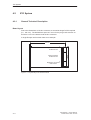
SMP16 System
2.4
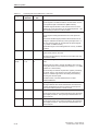
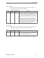
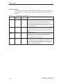
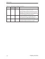
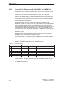
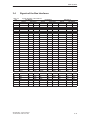
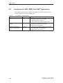
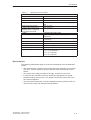
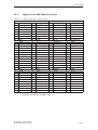
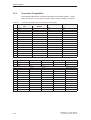
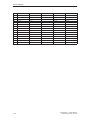
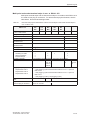
Table 2-4
Pin
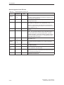
Signals of the Bus Interface
Signal assignment for the SMP16 bus
1
Pin Row A
Signal
Circuiting
–15 V
V2
–
Pin Row B
Signal
Circuiting
A16
V1
R1
Pin Row C
Signal
Circuiting
–12 V
V2
–
2
3
+3.3 V
–
V3
–
–
–
A17
AEN
V1
–
R1
–
GND
+5 V
V3
V3
–
–
4
5
6
CLK
MEMCS16*
RESET*
V1
V1
V1
R1
R1
R1
–
DREQ0*
DREQ1*
–
–
–
–
–
–
MMIO*
A12
A0
V1
V1
V1
R1
R1
R1
7
8
ALE
MEMR*
V1
V1
R1
R1/Z1
DACK0*
DACK1* 1)
–
–
–
–
A13
A1
V1
V1
R1
R1
9
10
11
RESIN*
MEMW*
–
V1
V1
–
–
R1/Z1
–
–
–
Reserved2)
–
–
–
–
–
–
A14
A2
A15
V1
V1
V1
R1
R1
R1
12
13
RDYIN
BUSEN
V1
V1
R1
R1
PWFAIL*
Reserved2)
–
–
–
R1
A3
NMI*
V1
–
R1
–
14
15
16
DB0
HOLDA 3)
DB1
V1
V1
V1
R1
R1
R1
+3.3 V
+5 V
GND
V3
V3
V3
–
–
–
A4
IRQ0*
A5
V1
–
V1
R1
–
R1
17
18
HOLD* 3)
DB2
V1
V1
R1
R1
GND
– 3)
V3
–
–
–
IRQ1*
A6
–
V1
R1
3) 4)
19
20
21
INT*
DB3
IOCS16*
V1
V1
V1
R1
R1
R1
ICAS0
ICAS1 3) 4)
ICAS2 3) 4)
–
–
–
–
–
–
IRQ2*
A7
IRQ3*
–
V1
–
–
R1
–
22
23
DB4
INTA*
V1
V1
R1
R1
DB8
DB9
V1
V1
R1
R1
A8
IRQ4*
V1
–
R1
–
24
25
26
DB5
UBAT
DB6
V1
V1
V1
R1
–
R1
DB10
DB11
DB12
V1
V1
V1
R1
R1
R1
A9
IRQ5*
A10
V1
–
V1
R1
–
R1
27
28
0WS
DB7
V1
V1
–
R1
DB13
DB14
V1
V1
R1
R1
IRQ6*
A11
–
V1
–
R1
29
30
31
TC/EOP*
IOW*
+15 V
V1
V1
V2
–
R1/Z1
–
DB15
BHEN
A18
V1
V1
V1
R1
R1
R1
IRQ7*
IOR*
GND
–
V1
V3
–
R1/Z1
–
+5 V
V3
–
A19
V1
R1
+12 V
V2
–
32
1)
2)
3)
4)
Is supplied by some CPUs as special signal OSC
Reserved for special signals ACEN (b11) and ACDONE (b13). See chapter 2.6.
Bus lines can also be used for DACK* and DREQ* signals or for DMA cascading.
Can be used to cascade interrupts (alternate to footnote 3)
SICOMP IMC – System Manual
J31069-D2001-U001-A0-7618
2–9