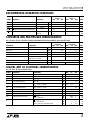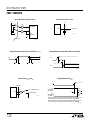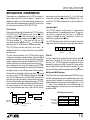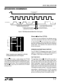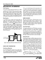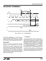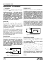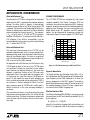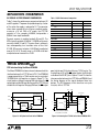
1
PCCtest 172 Technical Reference Manual M200052-03 January 2002 Preliminary Sycard Technology 1180-F Miraloma Way Sunnyvale, CA 94085 (408) 749-0130 (408) 749-1323 FAX http://www.sycard.com PCCtest 172 Technical Reference Manual Page 1 1. Introduction The PCCtest 172 16-bit PC Card tester is designed to provide manufacturers of PCMCIA based hosts a quick method of testing and verifying the operation of the PC Card sockets. The PCCtest is Type II PC Card that plugs into a standard PC Card Type II or III socket. The board is designed for both automated GO/NO-GO testing and component level debug. Test software is required on the host system. A custom ASIC is the core of the PCCtest 172. All testing logic is contained in this ASIC. The PCCtest contains an on-board A/D to provide accurate measurement of VCC and VPP voltages. Sycard Technology provides a DOS application to test Intel 82365SL compatible socket controllers. Simple command line invocation allows tests to be embedded into batch test files. OEMs that wish to use the PCCtest on a non-DOS platform can use this specification to develop custom test applications. 1.1 Differences between the PCCtest 172 and the PCCtest 170 Although the PCCtest 170 and the 172 appear to be the same, there are slight differences that make the PCCtest 172 suitable for certain applications. The PCCtest 172 was created to solve a problem with socket controllers that do not support 8 bit I/O windows (e.g. StrongArm SA-1100). On power-up the PCCtest 170 and 172 will put the WP/IOIS16# signal into a low state. Socket controllers that do not support 8 bit windows will use the IOIS16# signal to determine if the register is 16-bit or 8-bit. These socket controllers will not be able to access the odd numbered registers in the PCCtest 170. Since the control of the WP/IOIS16# is located in an odd numbered register (in the PCCtest 170) it is impossible to put the card into 8-bit mode. The PCCtest 172 solves this problem by placing the WP/IOIS16# control in an even numbered register. Table 1.1-1 illustrates the differences between the PCCtest 170 and 172. Control Bit WP/IOIS16# RDY/BSY/IREQ# ADCCE ADCLK PCCtest 170 PCCtest 172 MISC Register (offset 3) bit 6 CNTL Register (offset 4) bit 0 MISC Register (offset 3) bit 7 CNTL Register (offset 4) bit 1 CNTL Register (offset 4) bit 0 MISC Register (offset 3) bit 6 CNTL Register (offset 4) bit 1 MISC Register (offset 3) bit 7 Table 1.1-1 PCCtest 170 and 172 differences In addition to register changes, the PCCtest 172 CIS has been modified to identify the model. 2.0 Architecture of the PCCtest Figure 2.0-1 Illustrates the architecture of the PCCtest model 172. The functional blocks can be partitioned in to the following major sub-sections: • • Tester ASIC (Test ASIC) A/D Converter and Logic All interfaces to the PCCtest unit is via eight registers contained in the test ASIC. These eight registers control the various test functions contained within the PCCtest unit. The location at which these registers are accessed depends on which mode the PCCtest unit is in. On power-up, these test registers are located in attribute memory space. The test software can then enable I/O and/or common memory modes to test the various access modes of the PC Card interface. There are two major types of tests performed by the PCCtest unit - those implemented by the Test ASIC and the A/D tests. The Test ASIC based tests are designed to test the basic functionality of the interface. These tests will verify the basic operation of the interface including access strobes, data bus and address bus. Once these basic access modes are verified, the A/D test verifies the Vcc and Vpp levels. M200052-03 1994-2002 Sycard Technology Page 2 PCCtest 172 Technical Reference Manual Vcc Vpp1 A/D Vpp2 D[0..7] CIS EPROM A[0..7] A[0..25] Gate Array D[0..15] REG# CE1# CE2# WE# OE# WAIT# READY / IREQ# WP/IOIS16# IORD# IOWR# BVD1/STSCHG# BVD2/SPKR# VS1# INPACK# VS2# RESET 20MHz Figure 2.0-1 PCCtest 172 block diagram 1994-2002 Sycard Technology M200052-03 PCCtest 172 Technical Reference Manual Page 3 3.0 Testing the 16-bit PC Card Interface Most of the basic interface tests are handled in the Test ASIC. Eight registers control the operation of the Test ASIC. Appendix A lists the Test ASIC’s register description. Note that most write registers cannot be read back. It is up to the programmer to maintain an image of the write registers, since a read/modify/write operation is not possible for most of the register bits. Testing the 16-bit PC Card interface involves writing various test patterns to the PCCtest unit through the host socket controller. Status read back through these registers verify the functionality of the various portions of the interface. 3.1 Initializing the PCCtest The PCCtest must be powered through the host socket before any test operations can begin. The PCCtest model 172 can be powered to 3.3 or 5.0 Volts. The PCCtest 172 requires a power-on reset to initialize the internal operating circuitry. Care must be taken when switching operating voltages on the PCCtest. Do not switch from 3.3V to 5.0V or 5.0V to 3.3V without allowing the power to go to first go to 0V. The PCCtest on-board circuitry requires a minimum of 1200ms after Vcc is stable to initialize. Note: Vpp1 and Vpp2 can be measured by the PCCtest, but are not required for PCCtest operation. 3.2 Opening a Memory and I/O Window to the PCCtest In order to access the test resources in the PCCtest, an 8-bit attribute memory and an 8-bit I/O window must be opened to the PCCtest. Both an I/O and memory window is required to fully test the PC Card interface. The PCCtest contains eight 8-bit registers. These registers are accessed as 8 consecutive bytes. Note: For information on opening an I/O window, consult your socket controller chip user's manual. A memory window with a length of at least 8 bytes is required to test the interface's memory interface. Most socket controllers provide a minimum window length of 4K bytes. 3.2.1 PCCtest Memory and I/O Map The PCCtest 172 supports all three address spaces defined in the PC Card Standard. On power-up the PCCtest 172 responds to attribute memory accesses. Attribute memory reads from address 0H-FFH access the on-board Card Information Structure (CIS). The CIS contains tuples that identify the PCCtest 172. Appendix B contains a listing of the tuples contained in the CIS. Attribute Memory addresses 100H-107H contains the control registers used to test the PC Card Interface. The function of these registers are described in Appendix A. Attribute Space Description 0H – 0FFH Card Information Structure 100H – 107H Control Registers 108H-FFFFFFFH Control Registers (mirrored) Table 3.2-1 Attribute Memory Space The MODE register (offset 6) controls, which address spaces, the PCCtest responds to. Once the PCCtest unit it programmed out of its power-on mode, the control registers are accessed through I/O or common memory space. When accessing these registers in I/O or common memory mode, the registers appear at offset 0. Since there is no address decode for I/O or common memory mode, these registers are accessible on any 8 bit boundary. The following table describes the various PCCtest modes. M200052-03 1994-2002 Sycard Technology Page 4 PCCtest 172 Technical Reference Manual MODE.2 0 0 0 0 1 1 MODE.1 0 MODE.0 0 PCCtest Mode MODE 0 PCCtest operating mode Attribute memory space enabled, I/O and common memory accesses disabled 0 1 MODE 1 I/O space enabled, attribute and common memory space disabled 1 0 MODE 2 I/O space at 1F0H-1F7H enabled, attribute and common memory space disabled 1 1 MODE 3 I/O space at 170H-177H enabled, attribute and common memory space disabled 0 0 MODE 4 Common and attribute memory space enabled, I/O space disabled 0 1 MODE 5 Common memory and I/O space enabled. Attribute space disabled. Table 3.2-2 PCCtest modes accessed through MODE register Note: Once Mode 1, 2, 3 or 5 is enabled, all access to attribute memory space is disabled. Access to the PCCtest internal registers should be made through the enabled common memory or I/O space. Note: The RESET signal will NOT put the PCCtest into its power-on state. To reset the PCCtest unit, cycle power to the slot. 3.3 Preliminary Tests Before accessing the PCCtest hardware, the test software should verify the basic operation of the socket controller and that the PCCtest is properly inserted into the socket. This will avoid any unnecessary delays or erroneous error messages. The following sequence is used in Sycard's PCT172 software: 1. 2. 3. 4. 5. Verify socket controller is present by executing a simple register test. Power-up socket. Verify that the socket controller has powered up the slot (through the socket controller status) Wait 1200ms for PCCtest to initialize. Verify card detects are active (CD1# and CD2# are low) If any of these tests fail, further testing is not possible. 3.4 Basic Tests Once the socket controller has been verified and card detects are active, the PCCtest functions can be accessed. This part of the test procedure verifies the basic read/write operation of the card. If any failures are detected in the basic test, more advanced tests may return erroneous results. In order to run the first set of tests, an attribute memory window to the card must be opened. a) Read the CIS and compare with values contained in Appendix B. b) Basic 8-bit attribute memory read/write to the DATALO register - Verify basic 8-bit memory read. c) Basic 16-bit attribute memory read/write to the DATALO/DATAHI register - Verify basic 16-bit memory read. 1994-2002 Sycard Technology M200052-03 PCCtest 172 Technical Reference Manual Page 5 Once these tests pass, further more detailed tests can be run. Note: Basic 8-bit operation of the PCCtest requires the following signals to be working: D[7:0] OE# WE# CE1# A[2:0] 3.5 Data Tests The 16-bit PC Card data bus may be tested through several methods. When the PCCtest 172 is in MODE 0 the host writes data to the data latches DATALO at attribute memory offset 100H or DATAHI at 101H. Both 8 and 16 bit accesses are allowed. Data is latched into these registers on an attribute memory write to the DATALO and DATAHI registers. Once data is written, it can be read back to verify that all data bits that have been written are correct. The data pattern test can be also run via I/O or common memory accesses. The test software enables I/O or common memory accesses via the MODE register at attribute memory offset 106H. See table 3.2-2 for the valid modes. Data pattern tests can be run through attribute memory, common memory or I/O space depending on the setting of the MODE register. Common and attribute memory data pattern tests can be accomplished by accessing the same DATALO and DATAHI registers starting at offset 0 in I/O or memory space. On power-on reset access to these registers through the memory space are disabled. Prior to running the data test, the lower 8 bits of the data bus can be verified by reading the CIS data. A listing of the CIS is contained in Appendix B. 3.6 Address and REG# Tests Writing various address patterns to the PCCtest unit can test the PC Card’s 26-bit address bus. All address bits can be latched and read through the PC Card host interface. The address latching circuit must be armed prior to the access that triggers the latching circuitry. Addresses are latched on the falling edge of the control strobes, WE#, OE#, IORD#, or IOWR#. Note: The latching signal is a logical OR of the OE#, WE#, IORD# and IOWR# strobes qualified by either CE1# or CE2#. Arming of the address latches is accomplished through the ALAT bit in CNTL register (offset 4). A low to high transition of this bit will arm the latch. Any access after this arm will result in the latching of all 26-address signals on the interface. The following C code is used to arm the address latch: outportb(tester_addr+4,reg4_image & 0xfb); outportb(tester_addr+4,reg4_image | 0x04); Note: tester_addr is the base I/O address programmed into the host socket controller I/O mapping registers. M200052-03 1994-2002 Sycard Technology Page 6 PCCtest 172 Technical Reference Manual The latched values of the address and REG- signal may be read directly from the registers Signal Register Offset A[7:0] LADDRLO 4 A[15:8] LADDMID 5 A[23:16] LADDHI 2 A24 LATMISC.0 3 A25 LATMISC.7 3 CE1# STBLAT.2 7 CE2# STBLAT.3 7 OE# STBLAT.0 7 WE# STBLAT.1 7 IORD# STBLAT.4 7 IOWR# STBLAT.5 7 REG# LATMISC.5 3 Table 3.6-1 Address Latch Locations Description A0-A7 A8-A15 A16-A23 A24 A25 Latched CE1# Latched CE2# Latched OE# Latched WE# Latched IORD# Latched IOWR# Attribute Memory Select The following procedure is used to latch the address and read the data from the address latches to create a 26-bit address. 1. 2. 3. 4. 5. 6. 7. 8. Clear the ALAT bit in CNTL register at offset 4. Set the ALAT bit in the CNTL register. The address latch is now armed. Access the card with IORD#, IOWR#, OE# or WE# strobe. The address of the access is latched on the falling edge of the strobe. Read the lower 8 bits A[7:0] from the LADDRLO register at offset 4. Read the contents of the A[15:8] latch from the LADDMID register at offset 5. Read the contents of the A[23:16] latch from the LADDHI register at offset 2. Read the contents of the A[25:24] and REG# latch from the LATMISC register at offset 3. Read the contents of the CE1#, CE2# OE#,WE#,IORD#,IOWR# from the STBLAT register at offset 7. 3.7 Timing Measurements The PCCtest provides a flexible timing measurement circuit providing 50ns resolution. This circuit can measure from the rising/falling edge of any of the control strobes to the rising falling edge of the same set of signals. The following table lists the various control strobes that can be measured: Signal Description TCR Value OE# Memory Read Strobe 08H WE# Memory Write Strobe 19H IORD# I/O Read Strobe 6EH IOWR# I/O Write Strobe 7FH CE1# Chip Enable 1 2AH CE2# Chip Enable 2 3BH Table 3.7-1 Common Strobe Measurements TCR Values The signal and polarity that start the timer is selected via the STR[2:0] and the STRPOL bits in the TCR register. The STP[2:0] and STPPOL bits determine the signal that stops the timer. The following examples illustrate the values programmed into the TCR register (offset 2) for various timing measurements: 1994-2002 Sycard Technology M200052-03 PCCtest 172 Technical Reference Manual Page 7 Timing Measurement TCR Value Falling edge of CE1# to rising edge of OE# A0H Pulse width of IORD# 6EH Pulse width of IOWR# 7FH Rising edge of CE1# to rising edge of OE# 20H Pulse width of WE# 19H Table 3.7-2 Various Strobe Measurements TCR Values As with the address latching circuit, the timing logic is armed and the next access to the card is measured. The timing measurement is armed through an I/O write to the TRST register (offset 5). Once armed, the timer will start on first instance of the value programmed into the STR[2:0] register. The value can be read from the TIM register (offset 6). The value read from the TIM register is multiplied by the sample rate (50ns) to obtain the strobe width. 3.8 Testing RESET The RESET signal is an input to the PCCtest unit. RESET is only monitored by the PCCtest and will not reset the PCCtest. The current state of the RESET signal can be read from RESET bit in the LATMISC register (offset 3 bit 4). Testing of RESET involves forcing the state of RESET and reading the status in the RESET bit in the LATMISC register. In some socket controllers when RESET is asserted, the PC Card interface is tri-stated or disabled. In systems such as these, the previously described method of testing RESET will not work. With socket controllers such as these, the PCCtest 172 contains a RESET latch that stores the fact that a transition occurred RESET. The status of this latch can be read from LRESET bit in the STBLAT register (offset 7 bit 7). This latch is armed by setting, then clearing, the CLR_RST bit the CNTL register (offset 4 bit 4). Once the reset latch is armed the test software will then strobe the RESET signal from high to low. The latch will capture the low to high transition of the reset signal. Software can verify this by reading the LRESET bit in the STBLAT register 3.9 INPACK# Tests PCCtest can generate INPACK# on all I/O reads. Most socket controllers can use INPACK# to gate the PC Card data on to the host system data bus. Setting the INPKEN bit in the CNTL control register (offset 4 bit 3) enables INPACK# generation on all I/O reads. 3.10 Testing WAIT# A programmable wait state generator is used to generate wait states to simulate slow I/O or memory devices. The wait state generator is capable of generating wait states up to 3160ns. This covers the full range of PC card access times. Used in conjunction with the pulse measuring circuits can result in accurate measurement of read/write strobe widths. Timing for the wait state generator is based on the PCCtest main crystal (20Mhz). The wait state generator is accessed through WAIT[0:2] bits in the MISC control register at offset 3 bits [0:2]. In addition to the WAIT[0:2] bits, the WAITEN bit at offset 3 bit 3 must be set to enable wait states. M200052-03 1994-2002 Sycard Technology Page 8 PCCtest 172 Technical Reference Manual WAIT WAIT WAIT Time in ns 2 1 0 0 0 0 0 0 0 1 50 0 1 0 100 0 1 1 200 1 0 0 400 1 0 1 800 1 1 0 1650 1 1 1 3160 Table 3.10-1 Wait state delays 3.11 Testing BVD1 and BVD2 The BVD1 and BVD2 signal are outputs from the PCCtest card. They are implemented as parallel port bits in the CNTL register at offset 4. The host software writes various patterns to these bits and verifies continuity by reading the status through the socket controller's status registers. There are four bits used to control the BVD1 and BVD2 outputs. BVD1_EN# and BVD2_EN# must be set to 0 to enable the BVD1 and BVD2 tri-state outputs. The BVD1_OUT and BVD2_OUT bits control the state of the corresponding outputs. 3.12 Testing Ready and WP The RDY/BSY/IREQ# and WP/IOIS16# signal are outputs from the PCCtest card. They are implemented as parallel port bits in the CNTL register (offset 4 bits 1 and 0). The host software writes various patterns to these bits and verifies continuity by reading the status through the socket controller's status registers. 3.13 Testing Card Interrupts 1. 2. 3. 4. 5. 6. De-assert IREQ# by clearing RDY/BSY/IREQ# bit in MISC register (offset 4 bit 1). Configure interrupt routing in host socket controller for desired interrupt. Insert interrupt handler for desired interrupt. Assert interrupt by setting RDY/BSY/IREQ# bit in MISC register (offset 4 bit 1). Interrupt Service routine clears RDY/BSY/IREQ# bit to disable interrupt. Disable interrupt routing in host socket controller. 3.14 Testing Status Change (STSCHG#) Interrupts 1. 2. 3. 4. 5. 6. 7. Enable the BVD1 output by clearing BVD1_EN# in the CNTL register (offset 4 bit 4). De-assert STSCHG# by setting BVD1(STSCHG#) bit in CNTL register (offset 4 bit 5). Configure interrupt routing in host socket controller for desired interrupt. Insert interrupt handler for desired interrupt. Clear BVD1(STSCHG#) bit in CNTL register (offset 4 bit 5). Interrupt Service routine sets BVD1(STSCHG#) bit to disable interrupt. Disable interrupt routing in host socket controller. 3.15 Testing Voltage Sense (VS1# and VS2#) The PCCtest model 172 support testing of the VS1# and VS2# signals. On card initialization, VS1# and VS2# are both set inactive (high). VS1# and VS2# can be independently forced active (low) through the TCR register at offset 2. VS1# can be forced active (low) by setting STP[2:0] equal to 101. VS2# can be forced active (low) by setting STR[2:0] 1994-2002 Sycard Technology M200052-03 PCCtest 172 Technical Reference Manual Page 9 to 101. The test software is required to verify the state of VS1# and VS2# through the host controller’s status registers. 3.16 Speaker (SPKR#) Testing The PC Card’s digital audio output (SPKR#) can be tested by enabling the host socket controller’s speaker out signal. The host test software can then toggle the BVD2_OUT bit (offset 4 bit 7) at an audible frequency to verify the signal path between the PCCtest and the systems audio subsystem. In addition, the BVD2_EN# control (offset 4, bit 6) must be low to enable the SPKR# output. The test software is responsible for enabling the host socket controller’s speaker output pin and any other hardware required to enable the speaker drivers. 3.17 Identifying the PCCtest Test software can identify that a PCCtest unit has been inserted by reading the Card Information Structure (CIS). The CIS contains an ID string identifying the PCCtest along with the version of PCCtest hardware. Appendix B contains a listing of the PCCtest CIS. 3.18 Measuring Vcc, Vpp1 and Vpp2. The PCCtest 172 unit contains an on-board 8-bit A/D converter. An input analog multiplexer selects which voltage is to be measured. Figure 3.18-1 details the A/D converter subsystem. Vcc 3.01K 2.21K Vpp2 Vpp2 10.2K Vpp1 AMUX0 AMUX1 Vpp1 2.21K 1 2 Out +IN 2 Analog Mux 2.21K 10.2K 2.5V Reference 0 A Vref 5 LTC1196-2BCS A/D Converter Select B ADCCE 1 ADCLK 7 ADDAT 6 CS CLK Dout Figure 3.18-1 - PCCtest 172 A/D Subsystem The A/D converter I/O pins are controlled via internal register bits. The following control bits are tied to the A/D converter: Register Location Register Bit MISC.7 ADCLK MISC.6 ADCCE LATMISC.1 ADDAT MISC.5 AMUX0 CNTL.2 AMUX1 Table 3.18-1 A/D Control Bits Description Controls the A/D clock signal Controls the A/D chip enable signal A/D data output Analog Mux control bit 0 Analog Mux control bit 1 A four input analog multiplexer selects which voltage is to be measured: M200052-03 1994-2002 Sycard Technology Page 10 PCCtest 172 Technical Reference Manual A/D Input Select AMUX1 Vcc 0 Vpp2 0 Vpp1 1 Table 3.18-2 A/D Mux Control AMUX0 0 1 0 The A/D converter is implemented using the Linear Technology LTC1196. The programming interface to the A/D converter is contained in the LTC1196 data sheet. A copy of the LTC1196 datasheet is contained in Appendix C. 3.19 PCCtest 172 versions There are currently two versions of the PCCtest 170 in circulation. The following table describes the differences between the two: PCCtest 170 1.01 1.02 Description First release of the PCCtest 172. Second release of the PCCtest 172. CISTPL_CONFIG added to CIS 1994-2002 Sycard Technology M200052-03 Appendix A- Register Description Page A-1 Appendix A - Register Description This section describes the configuration of the PCCtest registers on initial power up. All PCCtest registers are written via attribute, memory or I/O write commands depending on the setting of the MODE register. There are eight writable 8-bit registers within the PCCtest unit. A[2:0] will select which register is written by the write strobe. The following table describes at which offset the PCCtest registers are located in each PCCtest mode. Mode 0 1 2 3 4 4 5 5 Space Attribute I/O I/O I/O Attribute Common Common I/O Register Offset 100H 0 1F0H 170H 100H 0 0 0 0 - DATALO - Low Data Byte to PC card bus Any memory write (WE#) qualified with a valid CE1# and A[0:2] = 000 will cause the DATALO register to be updated with contents of the PC card data bus (D[7:0]). In addition an I/O write qualified with CE1# and A[0:2] = 000 will also cause a write to this register Any memory read qualified with a valid CE1# will cause the value of the DATALO register to gated onto the PC card data bus (D[7:0]). An I/O read qualified with CE1# and A[0:2] = 000 will gate the contents of DATALO onto the PC Card data bus. 1 - DATAHI - High Data Byte to PC card bus Any memory write memory qualified with a valid CE2# will cause the DATAHI register to be updated with contents of the PC card data bus (D[15:7]). Note: An 8 bit I/O write to the DATAHI register is not possible. A memory read qualified with a valid CE2# will cause the value of the DATAHI register to be gated onto the PC card data bus (D[15:8). An 8 bit I/O read qualified by CE1# and A[0:2] = 001 will gate the contents of DATAHI onto the PC Card data bus D[7:0]. 2 - LADRHI – Address latch for A[23:16] (read) A read of this register returns the value of the specified latched address bits. Address is latched after the address latch circuitry is armed through the ADLAT bit located in the CNTL control register at offset 4. M200052-03 1994-2002 Sycard Technology Page A-2 Appendix A-Register Description 2 - TCR - Timer control register (write) The TCR is a write-only register that controls the operation of the strobe measurement circuitry. STR[2:0] selects the strobe that will cause the measurement to start. STRPOL selects which edge of the signal will start the timer. STP[2:0] selects the strobe that will stop the timer. STPPOL selects which edge terminates the timer. Bit D[2:0] Name STR[2:0] Description Start Pulse select STR2 STR1 STR0 Signal 0 0 0 OE# 0 0 1 WE# 0 1 0 CE1# 0 1 1 CE2# 1 0 0 Not Used 1 0 1 Force VS2# Low 1 1 0 IORD# 1 1 1 IOWR# D3 STRPOL Start polarity 0 - Start timer on positive edge 1 - Start timer on negative edge D[6:4] STP[2:0] End Pulse Select STP2 STP1 STP0 Signal 0 0 0 OE# 0 0 1 WE# 0 1 0 CE1# 0 1 1 CE2# 1 0 0 Not Used 1 0 1 Force VS1# Low 1 1 0 IORD# 1 1 1 IOWR# D7 STPPOL Stop polarity 0 - Stop timer on positive edge 1 - Stop timer on negative edge Table A-1: Register Offset 2H TCR - Timer Control Register 3 - LATMISC – Misc Latched Bits (read) The LATMISC register contains various realtime and latched status signals from the PC Card interface. Bit Name Description D0 LA24 Latched Address 24 D1 ADC Data A/D Data D2 BVD1_RB BVD1 Readback D3 BVD2_RB BVD2 Readback D4 RESET Unlatched Reset status D5 LREG# Latched REG# Signal D6 WP/IOIS16# WP/IOIS16# Readback D7 LA25 Latched Address 25 Table A-2: - LATMISC Register – Misc Latched Bits (Offset 3) 1994-2002 Sycard Technology M200052-03 Appendix A- Register Description Page A-3 3 - MISC - Control Register (write) The MISC Control register is a read/write register that contains various control bits for the PCCtest unit. Bit D[0:2] Name WAIT[0:2] Description Wait State Select – control the number of wait states that are inserted for any I/O or memory access. The wait state generator must be enabled through bit 3 of this register. WAIT2 WAIT1 WAIT0 Wait States 0 0 0 No wait states 0 0 1 50ns wait 0 1 0 100ns wait 0 1 1 200ns wait 1 0 0 400ns wait 1 0 1 800ns wait 1 1 0 1600ns wait 1 1 1 3200ns wait D3 ENWAIT Enable Wait State Generator D4 CIS Enable 0 = CIS ROM Enabled (Default) 1 = CIS ROM Disabled D5 AMUX0 A/D Mux Control bit 0 D6 ADCCE A/D Converter Chip Enable D7 ADCLK A/D Converter Clock Table A-3: MISC Register - Misc control bits (offset 3) 4 - LADRLO – Address latch for A[7:0] (read) A read of this register returns the value of the specified latched address bits. Address are latched after the address latch circuitry is armed through the ADLAT bit located in the CNTL control register at offset 4. 4 - CNTL – Control Register (write) CNTL is a write only register. Bit D0 D1 D2 Description WP/IOIS16# Output RDY/BSY and IREQ# output (inverted) Address Latch Enable A/D Mux control bit 1 D3 INPACK# Enable D4 0 = Enable BVD1/STSCHG# output 1 = Tri-state BVD1/STSCHG# output CLR_RST 1 = Clear LRESET bit in STBLAT.7. 0 = Arm reset latch D5 BVD1_OUT 0 = Force BVD1/STSCHG# output low 1 = Force BVD1/STSCHG# output high D6 BVD2_EN# 0 = Enable BVD2/SPKR# output 1 = Tri-state BVD2/SPKR# output D7 BVD2_OUT 0 = Force BVD2/SPKR# output low 1 = Force BVD2/SPKR# output high Table A-4: CNTL Register - Control Signal Latch (Offset 4) M200052-03 Name WP/IOIS16# RDY/BSY/IREQ# ALAT AMUX1 INPKEN BVD1_EN# 1994-2002 Sycard Technology Page A-4 Appendix A-Register Description 5 - LADRMID – Address latch for A[15:8] (read) A read of this register returns the value of the specified latched address bits. Address are latched after the address latch circuitry is armed through the ADLAT bit located in the CNTL control register (offset 4). 5 - TRST - Reset strobe to pulse counter A write to the TRST register will arm the strobe timer circuitry. Once a write to the TRST register is complete, the counter will be armed and waiting for the selected PC card strobe. 6 - TIM[0..7] - Timer Register (read) The Timer Register is a read-only register containing the results of the strobe timer. An 8-bit value represents the number of clocks that occurred between the selected start transition and the end transition specified in the TCR register. The actual value in nanoseconds can be calculated by multiplying the count by the sample clock period. The sample clock period for the PCCtest 172 is 50nS. The timer is armed by a write to the TRST register (offset 5). 6 - MODE – Mode Control Register (write) The mode control register is used to enable the various PCCtest test modes. Bits in this register enable common memory and I/O modes. Bit D[0:2] Name MODE [0:2] Description Mode Control MODE2 MODE1 MODE0 0 0 0 0 0 1 0 1 0 0 1 1 1 0 0 1 0 1 Mode 0 Mode 1 Mode 2 Mode 3 Mode 4 Mode 5 Description Attribute memory enabled, I/O space and common memory not enabled I/O space enabled, common and attribute memory disabled I/O space at 1F0H-1F7H enabled, common and attribute memory disabled I/O space at 170H-177H enabled, common and attribute memory disabled Common and attribute space enabled, I/O space disabled Common memory space enabled, I/O space enabled, attribute memory space disabled. D3 N.A. Not Used D4 N.A. Not Used D5 N.A. Not Used D6 N.A. Not Used D7 N.A. Not Used Table A-5: MODE Register - Mode Control Register (Offset 6) 1994-2002 Sycard Technology M200052-03 Appendix A- Register Description Page A-5 7 - STBLAT – Latched Control Bits (read) The STBLAT register is a read only register that contains the latched status of various control signals on the PC Card interface. All latched signal, except LRESET, are latched using the same mechanism at the address latch. Bit D0 D1 D2 D3 D4 D5 D6 D7 Description Latched OE# Latched WE# Latched CE1# Latched CE2# Latched IORD# Latched IOWR# Not Used Latched RESET status. Cleared by setting bit 4 in the CNTL register Table A-6: STBLAT Register - Latched Status Bits (read) M200052-03 Name LOE# LWE# LCE1# LCE2# LIORD# LIOWR# N.A. LRESET 1994-2002 Sycard Technology Appendix B-PCCtest 172 CIS Page B-1 Appendix B – PCCtest 172 Rev 1.01 CIS This section describes the Card Information Structure (CIS) stored in the attribute memory space of the PCCtest 172. Addr 00H 02H 04H Byte 01H 03H D1H 06H 08H 0AH 0FFH 0AH 0CH 0EH 10H 12H 14H 16H 18H 1AH 1CH 1EH 20H 22H 24H 26H 28H 2AH 2CH 2EH 30H 32H 34H 36H 38H 3AH 3CH 3EH 40H 42H 44H 46H 48H 4AH 4CH 4EH 50H 52H 54H 56H 58H 15H 30H 05H 00H 53H 79H 63H 61H 72H 64H 20H 54H 65H 63H 68H 6EH 6FH 6CH 6FH 67H 79H 00H 50H 43H 43H 74H 65H 73H 74H 00H 4DH 6FH 64H 65H 6CH 20H 31H 37H 32H 00H M200052-03 Description CISTPL_DEVICE Tuple link Device Info Field 1 - Function Specific Memory type 16K buffer @250nS 2 units of 8K = 16K End of tuple CISTPL_VERS_1 Tuple link TPLLV1_MAJOR TPLLV1_MINOR 'S' 'y' 'c' 'a' 'r' 'd' ' ' 'T' ‘e' 'c' 'h' 'n' 'o' 'l' 'o' 'g' 'y' 00H 'P' 'C' 'C' 't' 'e' 's' 't' 00H 'M' 'o' 'd' 'e' 'l' ' ' '1' '7' '2' 1994-2002 Sycard Technology Page B-2 Addr 5AH 5CH 5EH 60H 62H 64H 66H 68H 6AH 6CH 6EH 70H 72H 74H 76H 78H 7AH 7CH 7EH 80H 82H 84H 86H Appendix B-PCCtest 172 CIS Byte 52H 65H 76H 20H 31H 2EH 30H 31H 00H 0FFH 20H 04H 16H 02H 72H 01H 21H 02H FEH 00H 14H 00H 0FFH Description 'R' 'e' 'v' ' ' '1' '.' '0' '1' CISTPL_MFG_ID Tuple Link Manufacturer ID - LSB Manufacturer ID - MSB Product Number - LSB Product Number - MSB CISTPL_FUNC_ID Tuple Link CISTPL_NO_LINK CISTPL_END - That’s all folks 1994-2002 Sycard Technology M200052-03 Appendix B-PCCtest 172 CIS Page B-3 Appendix B.1 – PCCtest 172 Rev 1.02 CIS This section describes the Card Information Structure (CIS) stored in the attribute memory space of the PCCtest 172 Rev 1.02. Addr 00H 02H 04H Byte 01H 03H D1H 06H 08H 0AH 0FFH Description CISTPL_DEVICE Tuple link Device Info Field 1 - Function Specific Memory type 16K buffer @250nS 2 units of 8K = 16K End of tuple 0AH 0CH 0EH 10H 12H 14H 16H 18H 1AH 1CH 1EH 20H 22H 24H 26H 28H 2AH 2CH 2EH 30H 32H 34H 36H 38H 3AH 3CH 3EH 40H 42H 44H 46H 48H 4AH 4CH 4EH 50H 52H 54H 56H 15H 30H 05H 00H 53H 79H 63H 61H 72H 64H 20H 54H 65H 63H 68H 6EH 6FH 6CH 6FH 67H 79H 00H 50H 43H 43H 74H 65H 73H 74H 00H 4DH 6FH 64H 65H 6CH 20H 31H 37H 32H CISTPL_VERS_1 Tuple link TPLLV1_MAJOR TPLLV1_MINOR 'S' 'y' 'c' 'a' 'r' 'd' ' ' 'T' ‘e' 'c' 'h' 'n' 'o' 'l' 'o' 'g' 'y' 00H 'P' 'C' 'C' 't' 'e' 's' 't' 00H 'M' 'o' 'd' 'e' 'l' ' ' '1' '7' '2' M200052-03 1994-2002 Sycard Technology Page B-4 Addr 58H 5AH 5CH 5EH 60H 62H 64H 66H 68H 6AH 6CH 6EH 70H 72H 74H 76H 78H 7AH 7CH 7EH 80H 82H 84H 86H 88H 8AH 8CH 8EH 90H 92H 94H 96H 98H 9AH 9CH 9EH A0H A2H A4H A6H Appendix B-PCCtest 172 CIS Byte 00H 52H 65H 76H 20H 31H 2EH 30H 32H 00H 0FFH 20H 04H 16H 02H 72H 01H 21H 02H FEH 00H 1AH 05H 01H 01H 00H 02H 01H 1BH 07H C1H 01H 18H 63H 30H FFH FFH 14H 00H 0FFH Description 00H 'R' 'e' 'v' ' ' '1' '.' '0' '2' 00H CISTPL_MFG_ID Tuple Link Manufacturer ID - LSB Manufacturer ID - MSB Product Number - LSB Product Number - MSB CISTPL_FUNC_ID Tuple Link TPFID_FUNCTION - Vendor Specific Function CISTPL_CONFIG Tuple Link TPCC_SZ - Specify 2 byte address field TPCC__LAST Index value of last table entry tuple TPCC_RADR(LSB) Config register base address (0x200) TPCC_RADR(MSB) Config register base address (0x200) TPCC_RMSK - Register Mask TPCC_CFTABLE_ENTRY TPL_LINK TPL_INDEX TPCE_IF - Interface Definition Byte TPCE_FS - Feature Selection Byte TPCE_IO - I/O Window 8,16 bit, 3 address lines TPCE_IR - Interrupt Request Description (Level and Mask) TPCE_IR - Interrupt Mask 1 (All interrupts allowed) TPCE_IR - Interrupt Mask 2 (All interrupts allowed) CISTPL_NO_LINK CISTPL_END - That’s all folks 1994-2002 Sycard Technology M200052-03 Appendix C-Linear Technology LTC-1196 A/D Converter Page C-1 Appendix C – Linear Technology LTC-1196 A/D Converter M200052-03 1994-2002 Sycard Technology LTC1196/LTC1198 8-Bit, SO-8, 1MSPS ADCs with Auto-Shutdown Options U DESCRIPTIO FEATURES ■ ■ ■ ■ ■ ■ ■ ■ ■ ■ ■ ■ High Sampling Rates: 1MHz (LTC1196) 750kHz (LTC1198) Low Cost SO-8 Plastic Package Single Supply 3V and 5V Specifications Low Power: 10mW at 3V Supply 50mW at 5V Supply Auto-Shutdown: 1nA Typical (LTC1198) ±1/2LSB Total Unadjusted Error over Temperature 3-Wire Serial I/O 1V to 5V Input Span Range (LTC1196) Converts 1MHz Inputs to 7 Effective Bits Differential Inputs (LTC1196) 2-Channel MUX (LTC1198) ■ ■ ■ ■ The 3-wire serial I/O, SO-8 packages, 3V operation and extremely high sample rate-to-power ratio make these ADCs an ideal choice for compact, high speed systems. These ADCs can be used in ratiometric applications or with external references. The high impedance analog inputs and the ability to operate with reduced spans below 1V full scale (LTC1196) allow direct connection to signal sources in many applications, eliminating the need for gain stages. UO APPLICATI The LTC1196/LTC1198 are 600ns, 8-bit A/D converters with sampling rates up to 1MHz. They are offered in 8-pin SO packages and operate on 3V to 6V supplies. Power dissipation is only 10mW with a 3V supply or 50mW with a 5V supply. The LTC1198 automatically powers down to a typical supply current of 1nA whenever it is not performing conversions. These 8-bit switched-capacitor successive approximation ADCs include sample-and-holds. The LTC1196 has a differential analog input; the LTC1198 offers a software selectable 2-channel MUX. S High Speed Data Acquisition Disk Drives Portable or Compact Instrumentation Low Power or Battery-Operated Systems The A grade devices are specified with total unadjusted error of ±1/2LSB maximum over temperature. UO TYPICAL APPLICATI Single 5V Supply, 1MSPS, 8-Bit Sampling ADC 2 ANALOG INPUT 0V TO 5V RANGE CS VCC 8 7 LTC1196 CLK (SO-8) 3 6 –IN DOUT 4 5 GND VREF +IN SERIAL DATA LINK TO ASIC, PLD, MPU, DSP, OR SHIFT REGISTERS 1196/98 TA01 50 VREF = VCC = 2.7V fSMPL = 383kHz (LTC1196) fSMPL = 287kHz (LTC1198) 7 6 44 VREF = VCC = 5V fSMPL = 1MHz (LTC1196) fSMPL = 750kHz (LTC1198) 5 S/(N + D) (dB) 1 8 5V EFFECTIVE NUMBER OF BITS (ENOBs) 1µF Effective Bits and S/(N + D) vs Input Frequency 4 3 2 1 TA = 25°C 0 1k 10k 100k INPUT FREQUENCY (Hz) 1M 1196/98 G24 1 LTC1196/LTC1198 W W W AXI U U ABSOLUTE RATI GS (Notes 1, 2) Supply Voltage (VCC) to GND .................................... 7V Voltage Analog Reference ...................... –0.3V to VCC + 0.3V Digital Inputs.......................................... –0.3V to 7V Digital Outputs .......................... –0.3V to VCC + 0.3V Power Dissipation ............................................. 500mW Operating Temperature Range LTC1196-1AC, LTC1198-1AC, LTC1196-1BC, LTC1198-1BC, LTC1196-2AC, LTC1198-2AC, LTC1196-2BC, LTC1198-2BC................ 0°C to 70°C Storage Temperature Range ................ – 65°C to 150°C Lead Temperature (Soldering, 10 sec)................ 300°C W U U PACKAGE/ORDER I FOR ATIO ORDER PART NUMBER* ORDER PART NUMBER* TOP VIEW TOP VIEW CS 1 8 VCC +IN 2 7 CLK –IN 3 6 DOUT GND 4 5 VREF S8 PACKAGE 8-LEAD PLASTIC SOIC TJMAX = 150°C, θJA = 175°C/W LTC1196-1ACS8 LTC1196-1BCS8 LTC1196-2ACS8 LTC1196-2BCS8 CS/ 1 SHUTDOWN CH0 2 8 VCC (VREF) 7 CLK CH1 3 6 DOUT GND 4 5 DIN S8 PACKAGE 8-LEAD PLASTIC SOIC S8 PART MARKING 1961A 1961B 1962A 1962B LTC1198-1ACS8 LTC1198-1BCS8 LTC1198-2ACS8 LTC1198-2BCS8 S8 PART MARKING 1981A 1981B 1982A 1982B TJMAX = 150°C, θJA = 175°C/W *Parts available in N8 package. Consult factory for N8 samples. U U U U WW RECO E DED OPERATI G CO DITIO S SYMBOL PARAMETER VCC Supply Voltage CONDITIONS LTC1196-1 LTC1198-1 MIN TYP MAX LTC1196-2 LTC1198-2 MIN TYP MAX 2.7 6 2.7 6 0.01 0.01 14.4 12.0 0.01 0.01 12.0 9.6 UNITS V VCC = 5V Operation fCLK Clock Frequency ● tCYC Total Cycle Time tSMPL 12 16 12 16 CLK CLK Analog Input Sampling Time 2.5 2.5 CLK thCS Hold Time CS Low After Last CLK↑ 10 13 ns tsuCS Setup Time CS↓ Before First CLK↑ (See Figures 1, 2) 20 26 ns thDI Hold Time DIN After CLK↑ 20 26 ns 2 LTC1196 LTC1198 MHz MHz LTC1198 LTC1196/LTC1198 U U U U WW RECO E DED OPERATI G CO DITIO S SYMBOL PARAMETER CONDITIONS tsuDI Setup Time DIN Stable Before CLK↑ LTC1198 tWHCLK CLK High Time tWLCLK CLK Low Time tWHCS CS High Time Between Data Transfer Cycles tWLCS CS Low Time During Data Transfer LTC1196-1 LTC1198-1 MIN TYP MAX LTC1196-2 LTC1198-2 MIN TYP MAX UNITS 20 26 fCLK = fCLK(MAX) 40% 40% 1/fCLK fCLK = fCLK(MAX) 40% 40% 1/fCLK 25 32 ns 11 15 11 15 CLK CLK LTC1196 LTC1198 ns U U W CO VERTER A D ULTIPLEXER CHARACTERISTICS VCC = 5V, VREF = 5V, fCLK = fCLK(MAX) as defined in Recommended Operating Conditions, unless otherwise noted. PARAMETER LTC1196-XA LTC1198-XA MIN TYP MAX CONDITIONS No Missing Codes Resolution ● Offset Error Linearity Error (Note 3) Full-Scale Error Total Unadjusted Error (Note 4) LTC1196, VREF = 5.000V LTC1198, VCC = 5.000V Analog and REF Input Range LTC1196 Analog Input Leakage Current (Note 5) 8 LTC1196-XB LTC1198-XB MIN TYP MAX 8 UNITS Bits ● ±1/2 ±1 LSB ● ±1/2 ±1 LSB ● ±1/2 ±1 LSB ● ±1/2 ±1 LSB ±1 µA MAX UNITS – 0.05V to VCC + 0.05V ● V ±1 U DIGITAL A D DC ELECTRICAL CHARACTERISTICS VCC = 5V, VREF = 5V, unless otherwise noted. SYMBOL PARAMETER CONDITIONS MIN TYP VIH High Level Input Voltage VCC = 5.25V ● VIL Low Level Input Voltage VCC = 4.75V ● 0.8 V IIH High Level Input Current VIN = VCC ● 2.5 µA IIL Low Level Input Current VIN = 0V ● – 2.5 µA VOH High Level Output Voltage VCC = 4.75V, IO = 10µA VCC = 4.75V, IO = 360µA ● ● VOL Low Level Output Voltage VCC = 4.75V, IO = 1.6mA ● IOZ Hi-Z Output Leakage CS = High ● ISOURCE Output Source Current VOUT = 0V – 25 mA ISINK Output Sink Current VOUT = VCC 45 mA IREF Reference Current, LTC1196 CS = VCC fSMPL = fSMPL(MAX) ● ● 0.001 0.5 3 1 µA mA ICC Supply Current CS = VCC, LTC1198 (Shutdown) CS = VCC, LTC1196 fSMPL = fSMPL(MAX), LTC1196/LTC1198 ● ● ● 0.001 7 11 3 15 20 µA mA mA 2.0 4.5 2.4 V 4.74 4.71 V V 0.4 ±3 V µA 3 LTC1196/LTC1198 UW DY A IC ACCURACY VCC = 5V, VREF = 5V, fCLK = fCLK(MAX) as defined in Recommended Operating Conditions, unless otherwise noted. MIN LTC1198 TYP MAX PARAMETER CONDITIONS S/(N + D) Signal-to-Noise Plus Distortion 500kHz/1MHz Input Signal 47/45 47/45 dB THD Total Harmonic Distortion 500kHz/1MHz Input Signal 49/47 49/47 dB Peak Harmonic or Spurious Noise 500kHz/1MHz Input Signal 55/48 55/48 dB Intermodulation Distortion fIN1 = 499.37kHz, fIN2 = 502.446kHz 51 51 dB Full Power Bandwidth 8 8 MHz Full Linear Bandwidth [S/(N + D) > 44dB] 1 1 MHz IMD MIN LTC1196 TYP MAX SYMBOL UNITS AC CHARACTERISTICS VCC = 5V, VREF = 5V, fCLK = fCLK(MAX) as defined in Recommended Operating Conditions, unless otherwise noted. SYMBOL PARAMETER tCONV Conversion Time (See Figures 1, 2) CONDITIONS LTC1196-1 LTC1198-1 MIN TYP MAX LTC1196-2 LTC1198-2 MIN TYP MAX UNITS 600 710 710 900 ns ns ● fSMPL(MAX) Maximum Sampling Frequency tdDO Delay Time, CLK↑ to DOUT Data Valid LTC1196 LTC1196 LTC1198 LTC1198 1.20 1.00 0.90 0.75 ● ● CLOAD = 20pF 1.00 0.80 0.75 0.60 55 64 73 ● MHz MHz MHz MHz 68 78 94 ns ns tDIS Delay Time CS↑ to DOUT Hi-Z ● 70 120 88 150 ns ten Delay Time, CLK↓ to DOUT Enabled CLOAD = 20pF ● 30 50 43 63 ns thDO Time Output Data Remains Valid After CLK↑ CLOAD = 20pF ● tr DOUT Fall Time CLOAD = 20pF ● 5 15 10 20 ns tf DOUT Rise Time CLOAD = 20pF ● 5 15 10 20 ns CIN Input Capacitance Analog Input On Channel Analog Input Off Channel Digital Input 45 30 55 ns 30 5 5 30 5 5 pF pF pF LTC1196-1 LTC1198-1 MIN TYP MAX LTC1196-2 LTC1198-2 MIN TYP MAX 0.01 0.01 0.01 0.01 U U U U WW RECO 30 E DED OPERATI G CO DITIO S VCC = 2.7V Operation SYMBOL PARAMETER fCLK Clock Frequency CONDITIONS ● tCYC Total Cycle Time tSMPL thCS tsuCS 4 LTC1196 LTC1198 5.4 4.6 4 3 UNITS MHz MHz 12 16 12 16 CLK CLK Analog Input Sampling Time 2.5 2.5 CLK Hold Time CS Low After Last CLK↑ 20 40 ns Setup Time CS↓ Before First CLK↑ (See Figures 1, 2) 40 78 ns LTC1196/LTC1198 U U U U WW RECO E DED OPERATI G CO DITIO S VCC = 2.7V Operation LTC1196-1 LTC1198-1 MIN TYP MAX LTC1196-2 LTC1198-2 MIN TYP MAX SYMBOL PARAMETER CONDITIONS thDI Hold Time DIN After CLK↑ LTC1198 40 78 ns tsuDI Setup Time DIN Stable Before CLK↑ LTC1198 40 78 ns tWHCLK CLK High Time fCLK = fCLK(MAX) 40% 40% 1/fCLK tWLCLK CLK Low Time fCLK = fCLK(MAX) 40% 40% 1/fCLK tWHCS CS High Time Between Data Transfer Cycles 50 96 ns tWLCS CS Low Time During Data Transfer 11 15 11 15 CLK CLK LTC1196 LTC1198 UNITS U U W CO VERTER A D ULTIPLEXER CHARACTERISTICS VCC = 2.7V, VREF = 2.5V, fCLK = fCLK(MAX) as defined in Recommended Operating Conditions, unless otherwise noted. PARAMETER LTC1196-XA LTC1198-XA MIN TYP MAX CONDITIONS ● Offset Error ● ±1/2 ±1 ● ±1/2 ±1 LSB ● ±1/2 ±1 LSB ● ±1/2 ±1 LSB ±1 µA (Note 3) Full-Scale Error Total Unadjusted Error (Note 4) LTC1196, VREF = 2.500V LTC1198, VCC = 2.700V Analog and REF Input Range LTC1196 Analog Input Leakage Current (Note 5) 8 UNITS No Missing Codes Resolution Linearity Error 8 LTC1196-XB LTC1198-XB MIN TYP MAX Bits – 0.05V to VCC + 0.05V ● LSB V ±1 U DIGITAL A D DC ELECTRICAL CHARACTERISTICS VCC = 2.7V, VREF = 2.5V, unless otherwise noted. SYMBOL PARAMETER CONDITIONS MIN TYP MAX VIH High Level Input Voltage VCC = 3.6V ● VIL Low Level Input Voltage VCC = 2.7V ● 0.45 V IIH High Level Input Current VIN = VCC ● 2.5 µA IIL Low Level Input Current VIN = 0V ● – 2.5 µA VOH High Level Output Voltage VCC = 2.7V, IO = 10µA VCC = 2.7V, IO = 360µA ● ● VOL Low Level Output Voltage VCC = 2.7V, IO = 400µA ● IOZ Hi-Z Output Leakage CS = High ● ISOURCE Output Source Current VOUT = 0V ISINK Output Sink Current VOUT = VCC IREF Reference Current, LTC1196 CS = VCC fSMPL = fSMPL(MAX) ● ● 0.001 0.25 3.0 0.5 µA mA ICC Supply Current CS = VCC = 3.3V, LTC1198 (Shutdown) CS = VCC = 3.3V, LTC1196 fSMPL = fSMPL(MAX), LTC1196/LTC1198 ● ● ● 0.001 1.5 2.0 3.0 4.5 6.0 µA mA mA 1.9 2.3 2.1 UNITS V 2.60 2.45 V V 0.3 ±3 – 10 V µA mA 15 mA 5 LTC1196/LTC1198 UW DY A IC ACCURACY VCC = 2.7V, VREF = 2.5V, fCLK = fCLK(MAX) as defined in Recommended Operating Conditions, unless otherwise noted. CONDITIONS S/(N + D) Signal-to-Noise Plus Distortion 190kHz/380kHz Input Signal 47/45 47/45 dB THD Total Harmonic Distortion 190kHz/380kHz Input Signal 49/47 49/47 dB Peak Harmonic or Spurious Noise 190kHz/380kHz Input Signal 53/46 53/46 dB Intermodulation Distortion fIN1 = 189.37kHz, fIN2 = 192.446kHz 51 51 dB 5 5 MHz 0.5 0.5 MHz Full Power Bandwidth Full Linear Bandwidth [S/(N + D) > 44dB] MIN LTC1198 TYP MAX PARAMETER IMD MIN LTC1196 TYP MAX SYMBOL UNITS AC CHARACTERISTICS VCC = 2.7V, VREF = 2.5V, fCLK = fCLK(MAX) as defined in Recommended Operating Conditions, unless otherwise noted. SYMBOL PARAMETER tCONV Conversion Time (See Figures 1, 2) CONDITIONS LTC1196-1 LTC1198-1 MIN TYP MAX LTC1196-2 LTC1198-2 MIN TYP MAX UNITS 1.58 1.85 2.13 2.84 µs µs ● fSMPL(MAX) Maximum Sampling Frequency tdDO Delay Time, CLK↑ to DOUT Data Valid LTC1196 LTC1196 LTC1198 LTC1198 ● ● 450 383 337 287 CLOAD = 20pF 333 250 250 187 kHz kHz kHz kHz 100 150 180 130 200 250 ns ns ● 110 220 120 250 ns 80 130 100 200 ns ● tDIS Delay Time CS↑ to DOUT Hi-Z ten Delay Time, CLK↓ to DOUT Enabled CLOAD = 20pF ● thDO Time Output Data Remains Valid After CLK↑ CLOAD = 20pF ● tr DOUT Fall Time CLOAD = 20pF ● 10 30 15 40 ns tf DOUT Rise Time CLOAD = 20pF ● 10 30 15 40 ns CIN Input Capacitance Analog Input On Channel Analog Input Off Channel Digital Input The ● denotes specifications which apply over the full operating temperature range. Note 1: Absolute maximum ratings are those values beyond which the life of a device may be impaired. Note 2: All voltage values are with respect to GND. Note 3: Integral nonlinearity is defined as deviation of a code from a straight line passing through the actual endpoints of the transfer curve. The deviation is measured from the center of the quantization band. 6 45 90 30 5 5 45 120 ns 30 5 5 Note 4: Total unadjusted error includes offset, full scale, linearity, multiplexer and hold step errors. Note 5: Channel leakage current is measured after the channel selection. pF pF pF LTC1196/LTC1198 U W TYPICAL PERFOR A CE CHARACTERISTICS Supply Current vs Clock Rate Supply Current vs Supply Voltage 9 6 TA = 25°C CS = 0V VREF = VCC 4 3 VCC = 2.7V 2 “ACTIVE” MODE CS = 0V 8 LTC1196 LTC1198 6 4 2 1 0.000002 0 0 2 4 6 8 10 12 FREQUENCY (MHz) 14 16 LTC1198 0 2.5 3.0 3.5 4.0 4.5 5.0 SUPPLY VOLTAGE (V) Supply Current vs Temperature VCC = 5V 7 6 5 4 3 2 VCC = 2.7V 1 0 –55 –35 –15 MAGNITUDE OF OFFSET (LSB = 1 × VREF) 256 SUPPLY CURRENT (mA) 8 5.5 TA = 25°C 6.0 Offset vs Supply Voltage TA = 25°C VCC = 5V fCLK = 12MHz 1.2 TA = 25°C VREF = VCC fCLK = 3MHz 0.4 1.0 0.8 0.6 0.4 0.2 0.3 0.2 0.1 0 –0.1 –0.2 –0.3 –0.4 –0.5 2.5 Linearity Error vs Supply Voltage 0.5 0.4 0.3 0.2 0.1 0 –0.1 –0.2 –0.3 0.1 –0.4 0 0.5 1.0 1.5 2.0 2.5 3.0 3.5 4.0 4.5 5.0 REFERENCE VOLTAGE (V) 1196/98 G07 TA = 25°C VREF = VCC fCLK = 3MHz 0.3 0.2 6.0 5.5 0.5 0.4 LINEARITY ERROR (LSB) 0.6 3.5 4.0 4.5 5.0 SUPPLY VOLTAGE (V) Gain Error vs Reference Voltage 0.5 0.7 3.0 1196/98 G06 1196/98 G05 1.0 1M 10k 100k SAMPLE RATE (Hz) 1196/98 G03 0 0.5 1.0 1.5 2.0 2.5 3.0 3.5 4.0 4.5 5.0 REFERENCE VOLTAGE (V) 5 25 45 65 85 105 125 TEMPERATURE (°C) TA = 25°C VCC = 5V fCLK = 12MHz 1k 0.5 1.4 Linearity Error vs Reference Voltage LINEARITY ERROR (LSB) LT1198 VCC = 2.7V 0.01 0.001 100 1.6 1196/98 G04 0.8 LT1198 VCC = 5V 0.1 Offset vs Reference Voltage 10 CS = 0V LT1196 VCC = 2.7V 1196/98 G02 1196/98 G01 9 1 “SHUTDOWN” MODE CS = VCC MAGNITUDE OF GAIN ERROR (LSB) 5 10 MAGNITUDE OF OFFSET (LSB) 7 SUPPLY CURRENT (mA) 12 VCC = 5V SUPPLY CURRENT (mA) SUPPLY CURRENT (mA) LT1196 VCC = 5V TA = 25°C 8 0.9 Supply Current vs Sample Rate 10 14 TA = 25°C VCC = 5V fCLK = 12MHz 0.4 0.3 0.2 0.1 0 –0.1 –0.2 –0.3 –0.4 –0.5 2.5 3.0 3.5 4.0 4.5 5.0 SUPPLY VOLTAGE (V) 5.5 6.0 1196/98 G08 –0.5 0 0.5 1.0 1.5 2.0 2.5 3.0 3.5 4.0 4.5 5.0 REFERENCE VOLTAGE (V) 1196/98 G09 7 LTC1196/LTC1198 U W TYPICAL PERFOR A CE CHARACTERISTICS Maximum Clock Frequency vs Supply Voltage Gain vs Supply Voltage 18 19 0.3 0.2 0.1 0 –0.1 –0.2 –0.3 –0.4 –0.5 2.5 3.0 3.5 4.0 4.5 5.0 SUPPLY VOLTAGE (V) 5.5 TA = 25°C VREF = VCC 17 15 13 11 9 7 3.5 4.0 4.5 5.0 SUPPLY VOLTAGE (V) 60 50 40 30 20 10 0.15 0.10 RSOURCE+ VIN 1000 0.7 3.0 5.0 3.5 4.0 4.5 SUPPLY VOLTAGE (V) 5.5 100 1 6.0 6.0 1196/98 G16 100 10 1k SOURCE RESISTANCE (Ω) 1196/98 G15 DOUT Delay Time vs Temperature TA = 25°C VREF = VCC DOUT DELAY TIME, t dDO (ns) 140 100 80 60 40 0 2.5 10k 160 20 5.5 –IN 1196/98 G14 DOUT DELAY TIME, t dDO (ns) 0.9 +IN 0.05 120 1.1 100k TA = 25°C VCC = VREF = 5V 0.20 TA = 25°C 1.3 10 10k 1k 100 SOURCE RESISTANCE (Ω) 1196/98 G12 DOUT Delay Time vs Supply Voltage 1.5 120 VREF = VCC VCC = 2.7V 100 80 VCC = 5V 60 40 20 3.0 5.0 3.5 4.0 4.5 SUPPLY VOLTAGE (V) 5.5 6.0 1196/98 G17 *AS THE FREQUENCY IS DECREASED FROM 12MHz, MINIMUM CLOCK FREQUENCY (∆ERROR ≤ 0.1LSB) REPRESENTS THE FREQUENCY AT WHICH A 0.1LSB SHIFT IN ANY CODE TRANSITION FROM ITS 12MHz VALUE IS FIRST DETECTED. 8 1 140 5.0 3.5 4.0 4.5 SUPPLY VOLTAGE (V) TA = 25°C VCC = VREF = 5V Sample-and-Hold Acquisition Time vs Source Resistance 0.25 0 2.5 5 25 45 65 85 105 125 TEMPERATURE (°C) 1.9 3.0 4 10000 0.30 Digital Input Logic Threshold vs Supply Voltage 0.5 2.5 6 6.0 S&H ACQUISITION TIME (ns) PEAK-TO-PEAK ADC NOISE (LSB) MINIMUM CLOCK FREQUENCY (kHz) 70 1.7 –IN RSOURCE– TA = 25°C VREF = VCC 1196/98 G13 LOGIC THRESHOLD (V) 5.5 0.35 VCC = 5V VREF = 5V +IN 8 ADC Noise vs Reference and Supply Voltage 100 0 –55 –35 –15 VIN 10 1196/98 G11 Minimum Clock Rate for 0.1LSB* Error 80 12 0 3.0 1196/98 G10 90 14 2 5 2.5 6.0 16 CLOCK FREQUENCY (MHz) TA = 25°C fCLK = 3MHz VREF = VCC 0.4 MAXIMUM CLOCK FREQUENCY (MHz) MAGNITUDE OF GAIN ERROR (LSB) 0.5 Maximum Clock Frequency vs Source Resistance 0 – 60 –40 –20 0 20 40 60 80 100 120 140 TEMPERATURE (°C) 1196/98 G18 LTC1196/LTC1198 U W TYPICAL PERFOR A CE CHARACTERISTICS Input Channel Leakage Current vs Temperature Integral Nonlinearity vs Code at 5V LEAKAGE CURRENT (nA) 100 VCC = 5V VREF = 5V fCLK = 12MHz INTEGRAL NONLINEARITY ERROR (LSB) VCC = 5V VREF = 5V 10 ON CHANNEL 1 OFF CHANNEL 0.1 DIFFERENTIAL NONLINEARITY ERROR (LSB) 0.5 1000 0 –0.5 0.01 – 60 –40 –20 0 20 40 60 80 100 120 140 TEMPERATURE (°C) 0 32 0 –0.5 0 –0.5 0 32 64 7 6 4 3 2 1 VCC = 5V fIN = 29kHz fSMPL = 882kHz 96 128 160 192 224 256 CODE 1k 0 –20 –20 MAGNITUDE (dB) –30 –40 –50 –60 –30 –40 –50 –60 –70 –80 –80 –90 –90 –90 0 100 300 200 FREQUENCY (kHz) –100 400 500 1196/98 G25 –100 0 50 150 100 FREQUENCY (kHz) VCC = 5V fIN = 455kHz WITH 20kHz AM fSMPL = 1MHz –10 –70 –100 1M FFT Output of 455kHz AM Signal Digitized at 1MSPS –80 –70 10k 100k INPUT FREQUENCY (Hz) 1196/98 G24 VCC = 2.7V fIN = 29kHz fSMPL = 340kHz –10 MAGNITUDE (dB) –60 TA = 25°C 0 0 0 44 VREF = VCC = 5V fSMPL = 1MHz (LTC1196) fSMPL = 750kHz (LTC1198) 5 4096 Point FFT at 2.7V –50 50 VREF = VCC = 2.7V fSMPL = 383kHz (LTC1196) fSMPL = 287kHz (LTC1198) 1196/98 G23 4096 Point FFT Plot at 5V –40 96 128 160 192 224 256 CODE 8 VCC = 2.7V VREF = 2.5V fCLK = 3MHz 96 128 160 192 224 256 CODE –30 64 Effective Bits and S/(N + D) vs Input Frequency 0.5 1196/98 G22 –20 32 1196/98 G21 EFFECTIVE NUMBER OF BITS (ENOBs) DIFFERENTIAL NONLINEARITY ERROR (LSB) 0 –10 –0.5 S/(N + D) (dB) INL ERROR (LSB) VCC = 2.7V VREF = 2.5V fCLK = 3MHz 64 0 Differential Nonlinearity vs Code at 2.7V 0.5 32 VCC = 5V VREF = 5V fCLK = 12MHz 1196/98 G20 Integral Nonlinearity vs Code at 2.7V 0 0.5 96 128 160 192 224 256 CODE 64 1196/98 G19 MAGNITUDE (dB) Differential Nonlinearity vs Code at 5V 200 1196/98 G26 0 100 300 200 FREQUENCY (kHz) 400 500 1196/98 G27 9 LTC1196/LTC1198 U W TYPICAL PERFOR A CE CHARACTERISTICS Power Supply Feedthrough vs Ripple Frequency 0 TA = 25°C VCC (VRIPPLE = 20mV) fCLK = 12MHz –10 50 TA = 25°C VCC (VRIPPLE = 10mV) fCLK = 5MHz –10 FEEDTHROUGH(dB) –20 –30 –40 –50 SIGNAL TO NOISE PLUS DISTORTION (dB) 0 FEEDTHROUGH (dB) S/(N + D) vs Reference Voltage and Input Frequency Power Supply Feedthrough vs Ripple Frequency –20 –30 –40 –50 - –60 –60 –70 –70 10k 100k RIPPLE FREQUENCY (Hz) 1k 10k 100k RIPPLE FREQUENCY (Hz) 1k 1M 1M Intermodulation Distortion at 2.7V –70 SIGNAL TO NOISE-PLUS-DISTORTION (dB) MAGNITUDE (dB) MAGNITUDE (dB) –60 –30 –40 –50 –60 –70 –80 –80 –90 –90 –100 –100 150 100 FREQUENCY (kHz) 200 250 100 0 300 200 FREQUENCY (kHz) VREF = VCC = 5V fIN = 500kHz fSMPL = 1MHz 30 20 10 70 SPURIOUS-FREE DYNAMIC RANGE (dB) 80 VREF = VCC = 5V 60 VREF = VCC = 2.7V 40 20 VCC = 5V fCLK = 12MHz 60 50 VCC = 3V fCLK = 5MHz 40 30 20 10 TA = 25°C 0 1k 100k 10k 1M INPUT FREQUENCY (Hz) 10M 1k 10k 100k 1M 10M FREQUENCY (Hz) 1196/98 G34 –5 0 1196/98 G33 Spurious-Free Dynamic Range vs Frequency 100 PEAK-TO-PEAK OUTPUT (%) 40 0 –40 –35 –30 –25 –20 –15 –10 INPUT LEVEL (dB) 400 Output Amplitude vs Input Frequency 10 VCC = 5V 25 1.25 1.75 2.25 2.75 3.25 3.75 4.25 4.75 5.25 REFERENCE VOLTAGE (V) 1196/98 G32 1196/98 G31 0 30 S/(N + D) vs Input Level VCC = 5V f1 = 200kHz f2 = 210kHz fSMPL = 750kHz –20 –50 50 35 50 –10 –40 0 40 Intermodulation Distortion at 5V VCC = 2.7V f1 = 100kHz f2 = 110kHz fSMPL = 420kHz –30 fIN = 500kHz 1196/98 G30 0 0 –20 fIN = 200kHz fIN = 100kHz 1196/98 G29 1196/98 G28 –10 45 1196/98 G35 LTC1196/LTC1198 U U U PI FU CTIO S LTC1196 LTC1198 CS (Pin 1): Chip Select Input. A logic low on this input enables the LTC1196. A logic high on this input disables the LTC1196. CS/SHUTDOWN (Pin 1): Chip Select Input. A logic low on this input enables the LTC1198. A logic high on this input disables the LTC1198 and DISCONNECTS THE POWER TO THE LTC1198. IN + (Pin 2): Analog Input. This input must be free of noise with respect to GND. CHO (Pin 2): Analog Input. This input must be free of noise with respect to GND. IN – (Pin 3): Analog Input. This input must be free of noise with respect to GND. GND (Pin 4): Analog Ground. GND should be tied directly to an analog ground plane. VREF (Pin 5): Reference Input. The reference input defines the span of the A/D converter and must be kept free of noise with respect to GND. CH1 (Pin 3): Analog Input. This input must be free of noise with respect to GND. GND (Pin 4): Analog Ground. GND should be tied directly to an analog ground plane. DIN (Pin 5): Digital Data Input. The multiplexer address is shifted into this input. DOUT (Pin 6): Digital Data Output. The A/D conversion result is shifted out of this output. DOUT (Pin 6): Digital Data Output. The A/D conversion result is shifted out of this output. CLK (Pin 7): Shift Clock. This clock synchronizes the serial data transfer. CLK (Pin 7): Shift Clock. This clock synchronizes the serial data transfer. VCC (Pin 8): Power Supply Voltage. This pin provides power to the A/D converter. It must be kept free of noise and ripple by bypassing directly to the analog ground plane. VCC(VREF)(Pin 8): Power Supply and Reference Voltage. This pin provides power and defines the span of the A/D converter. It must be kept free of noise and ripple by bypassing directly to the analog ground plane. W BLOCK DIAGRA CS (CS/SHUTDOWN) CLK VCC (VCC/VREF) BIAS AND SHUTDOWN CIRCUIT IN + (CH0) CSMPL IN – (CH1) SERIAL PORT DOUT – + SAR HIGH SPEED COMPARATOR CAPACITIVE DAC GND PIN NAMES IN PARENTHESES REFER TO THE LTC1198 VREF (DIN) 1196/98 BD 11 LTC1196/LTC1198 TEST CIRCUITS Load Circuit for t dDO, t r and t f On and Off Channel Leakage Current 5V 1.4V ION A 3k ON CHANNEL DOUT IOFF TEST POINT A 100pF • • • • OFF CHANNEL 1196/98 TC02 POLARITY 1196/98 TC01 Voltage Waveform for DOUT Rise and Fall Times, tr, tf Voltage Waveform for DOUT Delay Time, tdDO and thDO VOH DOUT VIH CLK VOL tr tdDO thDO tf 1196/98 TC04 VOH DOUT VOL 1196/98 TC03 Load Circuit for tdis and ten Voltage Waveforms for tdis VIH CS TEST POINT 3k VCC tdis WAVEFORM 2, ten DOUT 20pF tdis WAVEFORM 1 1196/98 TC05 DOUT WAVEFORM 1 (SEE NOTE 1) 90% tdis DOUT WAVEFORM 2 (SEE NOTE 2) 10% NOTE 1: WAVEFORM 1 IS FOR AN OUTPUT WITH INTERNAL CONDITIONS SUCH THAT THE OUTPUT IS HIGH UNLESS DISABLED BY THE OUTPUT CONTROL. NOTE 2: WAVEFORM 2 IS FOR AN OUTPUT WITH INTERNAL CONDITIONS SUCH THAT THE OUTPUT IS LOW UNLESS DISABLED BY THE OUTPUT CONTROL. 1196/98 TC06 12 LTC1196/LTC1198 TEST CIRCUITS Voltage Waveforms for ten LTC1196 CS CLK 2 1 3 4 B7 DOUT VOL 1196/98 TC07 ten Voltage Waveforms for ten LTC1198 CS DIN CLK START 1 2 3 5 4 6 7 B7 DOUT VOL ten 1196/98 TC08 13 LTC1196/LTC1198 W U U UO APPLICATI S I FOR ATIO OVERVIEW LTC1198 has a 2-channel input multiplexer and can convert either channel with respect to ground or the difference between the two. It also automatically powers down when not performing conversion, drawing only leakage current. The LTC1196/LTC1198 are 600ns sampling 8-bit A/D converters packaged in tiny 8-pin SO packages and operating on 3V to 6V supplies. The ADCs draw only 10mW from a 3V supply or 50mW from a 5V supply. SERIAL INTERFACE Both the LTC1196 and the LTC1198 contain an 8-bit, switched-capacitor ADC, a sample-and-hold, and a serial port (see Block Diagram). The on-chip sample-and-holds have full-accuracy input bandwidths of 1MHz. Although they share the same basic design, the LTC1196 and LTC1198 differ in some respects. The LTC1196 has a differential input and has an external reference input pin. It can measure signals floating on a DC common-mode voltage and can operate with reduced spans below 1V. The The LTC1196/LTC1198 will interface via three or four wires to ASICs, PLDs, microprocessors, DSPs, or shift registers (see Operating Sequence in Figures 1 and 2). To run at their fastest conversion rates (600ns), they must be clocked at 14.4MHz. HC logic families and any high speed ASIC or PLD will easily interface to the ADCs at that speed (see Data Transfer and Typical Application sections). Full speed operation from a 3V supply can still be achieved with 3V ASICs, PLDs or HC logic circuits. tCYC (12 CLKs) CS tsuCS CLK tdDO DOUT B0 B7 NULL BITS Hi-Z B6 B5 B4 B3 B2 B1 B0* tCONV (8.5 CLKs) tSMPL NULL BITS Hi-Z tSMPL *AFTER COMPLETING THE DATA TRANSFER, IF FURTHER CLOCKS ARE APPLIED WITH CS LOW, THE ADC WILL OUTPUT ZEROS INDEFINITELY. 1196/98 F01 Figure 1. LTC1196 Operating Sequence tCYC (16 CLKs) CS POWER DOWN tsuCS CLK ODD/ SIGN START DUMMY DON’T CARE DIN SGL/ DIFF DOUT DUMMY tdDO NULL BITS HI-Z tSMPL (2.5CLKs) B7 B6 B5 B4 B3 B2 B1 B0* Hi-Z tCONV (8.5CLKs) *AFTER COMPLETING THE DATA TRANSFER, IF FURTHER CLOCKS ARE APPLIED WITH CS LOW, THE ADC WILL OUTPUT ZEROS INDEFINITELY. 1196/98 F02 Figure 2. LTC1198 Operating Sequence Example: Differential Inputs (CH 1, CH 0) 14 LTC1196/LTC1198 W U U UO APPLICATI S I FOR ATIO Connection to a microprocessor or a DSP serial port is quite simple (see Data Transfer section). It requires no additional hardware, but the speed will be limited by the clock rate of the microprocessor or the DSP which limits the conversion time of the LTC1196/LTC1198. conversion result are output on the DOUT line. At the end of the data exchange CS should be brought high. This resets the LTC1198 in preparation for the next data exchange. Input Data Word Data Transfer Data transfer differs slightly between the LTC1196 and the LTC1198. The LTC1196 interfaces over 3 lines: CS, CLK and DOUT. A falling CS initiates data transfer as shown in the LTC1196 Operating Sequence. After CS falls, the first CLK pulse enables DOUT. After two null bits, the A/D conversion result is output on the DOUT line. Bringing CS high resets the LTC1196 for the next data exchange. The LTC1196 requires no DIN word. It is permanently configured to have a single differential input. The conversion result is output on the DOUT line in an MSB-first sequence, followed by zeros indefinitely if clocks are continuously applied with CS low. The LTC1198 clocks data into the DIN input on the rising edge of the clock. The input data word is defined as follows: The LTC1198 can transfer data with 3 or 4 wires. The additional input, DIN, is used to select the 2-channel MUX configuration. START SGL/ DIFF ODD/ SIGN DUMMY DUMMY MUX ADDRESS DUMMY BITS 119698 AI02 The data transfer between the LTC1198 and the digital systems can be broken into two sections: Input Data Word and A/D Conversion Result. First, each bit of the input data word is captured on the rising CLK edge by the LTC1198. Second, each bit of the A/D conversion result on the DOUT line is updated on the rising CLK edge by the LTC1198. This bit should be captured on the next rising CLK edge by the digital systems (see A/D Conversion Result section). Start Bit Data transfer is initiated by a falling chip select (CS) signal as shown in the LTC1198 Operating Sequence. After CS falls the LTC1198 looks for a start bit. After the start bit is received, the 4-bit input word is shifted into the DIN input. The first two bits of the input word configure the LTC1198. The last two bits of the input word allow the ADC to acquire the input voltage by 2.5 clocks before the conversion starts. After the conversion starts, two null bits and the Multiplexer (MUX) Address The first “logical one” clocked into the DIN input after CS goes low is the start bit. The start bit initiates the data transfer. The LTC1198 will ignore all leading zeros which precede this logical one. After the start bit is received, the remaining bits of the input word will be clocked in. Further inputs on the DIN pin are then ignored until the next CS cycle. The 2 bits of the input word following the START bit assign the MUX configuration for the requested conversion. For a given channel selection, the converter will measure the voltage between the two channels indicated by the “+” and “–” signs in the selected row of the following table. In single-ended mode, all input channels are measured with respect to GND. CS LTC1198 Channel Selection DIN1 DIN2 DOUT1 DOUT2 SINGLE-ENDED MUX MODE SHIFT MUX ADDRESS IN 2 NULL BITS DIFFERENTIAL MUX MODE SHIFT A/D CONVERSION RESULT OUT MUX ADDRESS SGL/DIFF ODD/SIGN 1 0 1 1 0 0 0 1 CHANNEL # 0 1 + + + – – + GND – – 1196/98 AI03 1196/98 AI01 15 LTC1196/LTC1198 W U U UO APPLICATI S I FOR ATIO Dummy Bits Unipolar Output Code The last 2 bits of the input word following the MUX Address are dummy bits. Either bit can be a “logical one” or a “logical zero.” These 2 bits allow the ADC 2.5 clocks to acquire the input signal after the channel selection. OUTPUT CODE INPUT VOLTAGE INPUT VOLTAGE (VREF = 5.000V) 11111111 11111110 • • • 00000001 00000000 VREF – 1LSB VREF – 2LSB • • • 1LSB 0V 4.9805V 4.9609V • • • 0.0195V 0V 1196/98 AI05 A/D Conversion Result Both the LTC1196 and the LTC1198 have the A/D conversion result appear on the DOUT line after two null bits (see Operating Sequence in Figures 1 and 2). Data on the DOUT line is updated on the rising edge of the CLK line. The DOUT data should also be captured on the rising CLK edge by the digital systems. Data on the DOUT line remains valid for a minimum time of thDO (30ns at 5V) to allow the capture to occur (see Figure 3). VIH CLK tdDO thDO VOH DOUT VOL Operation with DIN and DOUT Tied Together The LTC1198 can be operated with DIN and DOUT tied together. This eliminates one of the lines required to communicate to the digital systems. Data is transmitted in both directions on a single wire. The pin of the digital systems connected to this data line should be configurable as either an input or an output. The LTC1198 will take control of the data line and drive it low on the 5th falling CLK edge after the start bit is received (see Figure 4). Therefore the port line of the digital systems must be switched to an input before this happens to avoid a conflict. REDUCING POWER CONSUMPTION 1196/98 TC03 Figure 3. Voltage Waveform for DOUT Delay Time, tdDO and thDO Unipolar Transfer Curve The LTC1196/LTC1198 are permanently configured for unipolar only. The input span and code assignment for this conversion type are shown in the following figures. The LTC1196/LTC1198 can sample at up to a 1MHz rate, drawing only 50mW from a 5V supply. Power consumption can be reduced in two ways. Using a 3V supply lowers the power consumption on both devices by a factor of five, to 10mW. The LTC1198 can reduce power even further because it shuts down whenever it is not converting. Figure 5 shows the supply current versus sample rate for the LTC1196 and LTC1198 on 3V and 5V. To achieve such a low power consumption, especially for the LTC1198, several things must be taken into consideration. Unipolar Transfer Curve Shutdown (LTC1198) 11111111 11111110 • • • 00000001 00000000 VIN VREF VREF – 1LSB VREF – 2LSB 1LSB 0V 16 1196/98 AI04 Figure 2 shows the operating sequence of the LTC1198. The converter draws power when the CS pin is low and powers itself down when that pin is high. For lowest power consumption in shutdown, the CS pin should be driven with CMOS levels (0V to VCC) so that the CS input buffer of the converter will not draw current. LTC1196/LTC1198 W U U UO APPLICATI S I FOR ATIO DUMMY BITS LATCHED BY LTC1198 CS 1 2 3 4 5 START SGL/DIFF ODD/SIGN DUMMY DUMMY CLK DATA (DIN/DOUT) THE DIGITAL SYSTEM CONTROLS DATA LINE AND SENDS MUX ADDRESS TO LTC1198 B7 B6 LTC1198 CONTROLS DATA LINE AND SENDS A/D RESULT BACK TO THE DIGITAL SYSTEM THE DIGITAL SYSTEM MUST RELEASE DATA LINE AFTER 5TH RISING CLK AND BEFORE THE 5TH FALLING CLK LTC1198 TAKES CONTROL OF DATA LINE ON 5TH FALLING CLK 1196/98 F04 Figure 4. LTC1198 Operation with DIN and DOUT Tied Together 10 Minimize CS Low Time (LTC1198) SUPPLY CURRENT (mA) LT1196 VCC = 5V 1 0.1 LT1198 VCC = 5V LT1198 VCC = 2.7V 0.01 0.001 100 In systems that have significant time between conversions, lowest power drain will occur with the minimum CS low time. Bringing CS low, transfering data as quickly as possible, then bringing it back high will result in the lowest current drain. This minimizes the amount of time the device draws power. LT1196 VCC = 2.7V OPERATING ON OTHER THAN 5V SUPPLIES 1k 10k 100k SAMPLE RATE (Hz) 1M 1196/98 F05 Figure 5. Supply Current vs Sample Rate for LTC1196/ LTC1198 Operating on 5V and 2.7V Supplies The LTC1196/LTC1198 operate from single 2.7V to 6V supplies. To operate the LTC1196/LTC1198 on other than 5V supplies, a few things must be kept in mind. Input Logic Levels When the CS pin is high (= supply voltage), the LTC1198 is in shutdown mode and draws only leakage current. The status of the DIN and CLK input has no effect on the supply current during this time. There is no need to stop DIN and CLK with CS = high; they can continue to run without drawing current. The input logic levels of CS, CLK and DIN are made to meet TTL on 5V supply. When the supply voltage varies, the input logic levels also change (see typical curve of Digital Input Logic Threshold vs Supply Voltage). For these two ADCs to sample and convert correctly, the digital inputs have to be in the logical low and high relative to the operating supply voltage. If achieving micropower consumption is desirable on the LTC1198, the digital inputs must go rail-to-rail between supply voltage and ground (see Reducing Power Consumption section). 17 LTC1196/LTC1198 W U U UO APPLICATI S I FOR ATIO Clock Frequency The maximum recommended clock frequency is 14.4MHz at 25°C for the LTC1196/LTC1198 running off a 5V supply. With the supply voltage changing, the maximum clock frequency for the devices also changes (see the typical curve of Maximum Clock Rate vs Supply Voltage). If the supply is reduced, the clock rate must be reduced also. At 3V the devices are specified with a 5.4MHz clock at 25°C. The VCC pin should be bypassed to the ground plane with a 1µF tantalum with leads as short as possible. If the power supply is clean, the LTC1196/LTC1198 can also operate with smaller 0.1µF surface mount or ceramic bypass capacitors. All analog inputs should be referenced directly to the single-point ground. Digital inputs and outputs should be shielded from and/or routed away from the reference and analog circuitry. Mixed Supplies SAMPLE-AND-HOLD It is possible to have a digital system running off a 5V supply and communicate with the LTC1196/LTC1198 operating on a 3V supply. Achieving this reduces the outputs of DOUT from the ADCs to toggle the equivalent input of the digital system. The CS, CLK and DIN inputs of the ADCs will take 5V signals from the digital system without causing any problem (see typical curve of Digital Input Logic Threshold vs Supply Voltage). With the LTC1196 operating on a 3V supply, the output of DOUT only goes between 0V and 3V. This signal easily meets TTL levels (see Figure 6). Both the LTC1196 and the LTC1198 provide a built-in sample-and-hold (S&H) function to acquire the input signal. The S&H acquires the input signal from “+” input during tSMPL as shown in Figures 1 and 2. The S&H of the LTC1198 can sample input signals in either single-ended or differential mode (see Figure 7). 3V 4.7µF MPU (e.g., 8051) DIFFERENTIAL INPUTS COMMON-MODE RANGE 0V TO 3V CS VCC P1.4 +IN CLK P1.3 –IN DOUT P1.2 GND VREF LTC1196 5V The sample-and-hold of the LTC1198 allows conversion of rapidly varying signals. The input voltage is sampled during the tSMPL time as shown in Figure 7. The sampling interval begins as the bit preceding the first DUMMY bit is shifted in and continues until the falling CLK edge after the second DUMMY bit is received. On this falling edge, the S&H goes into hold mode and the conversion begins. Differential Inputs 3V 1196/98 F06 Figure 6. Interfacing a 3V Powered LTC1196 to a 5V System BOARD LAYOUT CONSIDERATIONS Grounding and Bypassing The LTC1196/LTC1198 are easy to use if some care is taken. They should be used with an analog ground plane and single-point grounding techniques. The GND pin should be tied directly to the ground plane. 18 Single-Ended Inputs With differential inputs, the ADC no longer converts just a single voltage but rather the difference between two voltages. In this case, the voltage on the selected “+” input is still sampled and held and therefore may be rapidly time varying just as in single-ended mode. However, the voltage on the selected “–” input must remain constant and be free of noise and ripple throughout the conversion time. Otherwise, the differencing operation may not be performed accurately. The conversion time is 8.5 CLK cycles. Therefore, a change in the “–” input voltage during this interval can cause conversion errors. For a sinusoidal voltage on the “–” input, this error would be: VERROR (MAX) = VPEAK × 2 × π × f(“–”) × 8.5/fCLK Where f(“–”) is the frequency of the “–” input voltage, VPEAK is its peak amplitude and fCLK is the frequency of the LTC1196/LTC1198 U W U UO APPLICATI S I FOR ATIO SAMPLE HOLD “+” INPUT MUST SETTLE DURING THIS TIME CS tSMPL tCONV CLK DIN START SGL/DIFF ODD/SIGN DUMMY DUMMY DON’T CARE B7 DOUT 1ST BIT TEST “–” INPUT MUST SETTLE DURING THIS TIME “+” INPUT “–” INPUT 1196/98 F07 Figure 7. LTC1198 “+” and “–” Input Settling Windows CLK. VERROR is proportional to f(“–”) and inversely proportional to fCLK. For a 60Hz signal on the “–” input to generate a 1/4LSB error (5mV) with the converter running at CLK = 12MHz, its peak value would have to be 18.7V. ANALOG INPUTS Because of the capacitive redistribution A/D conversion techniques used, the analog inputs of the LTC1196/ LTC1198 have one capacitive switching input current spike per conversion. These current spikes settle quickly and do not cause a problem. However, if source resistances larger than 100Ω are used or if slow settling op amps drive the inputs, care must be taken to insure that the transients caused by the current spikes settle completely before the conversion begins. “+” Input Settling The input capacitor of the LTC1196 is switched onto “+” input at the end of the conversion and samples the input signal until the conversion begins (see Figure 1). The input capacitor of the LTC1198 is switched onto “+” input during the sample phase (tSMPL, see Figure 7). The sample phase is 2.5 CLK cycles before conversion starts. The voltage on the “+” input must settle completely within tSMPL for the LTC1196/LTC1198. Minimizing RSOURCE+ will improve the input settling time. If a large “+” input source resistance must be used, the sample time can be increased by allowing more time between conversions for the LTC1196 or by using a slower CLK frequency for the LTC1198. 19 LTC1196/LTC1198 W U U UO APPLICATI S I FOR ATIO “–” Input Settling REFERENCE INPUT At the end of the tSMPL, the input capacitor switches to the “–” input and conversion starts (see Figures 1 and 7). During the conversion, the “+” input voltage is effectively “held” by the sample-and-hold and will not affect the conversion result. However, it is critical that the “–” input voltage settle completely during the first CLK cycle of the conversion time and be free of noise. Minimizing RSOURCE– will improve settling time. If a large “–” input source resistance must be used, the time allowed for settling can be extended by using a slower CLK frequency. The voltage on the reference input of the LTC1196 defines the voltage span of the A/D converter. The reference input has transient capacitive switching currents which are due to the switched-capacitor conversion technique (see Figure 9). During each bit test of the conversion (every CLK cycle), a capacitive current spike will be generated on the reference pin by the ADC. These high frequency current spikes will settle quickly and do not cause a problem if the reference input is bypassed with at least a 0.1µF capacitor. Input Op Amps When driving the analog inputs with an op amp it is important that the op amp settle within the allowed time (see Figures 1 and 7). Again, the “+” and “–” input sampling times can be extended as described above to accommodate slower op amps. The reference input can be driven with standard voltage references. Bypassing the reference with a 0.1µF capacitor is recommended to keep the high frequency impedance low as described above. Some references require a small resistor in series with the bypass capacitor for frequency stability. See the individual reference data sheet for details. REF+ 5 To achieve the full sampling rate, the analog input should be driven with a low impedance source (<100Ω) or a high speed op amp (e.g., the LT1223, LT1191, or LT1226). Higher impedance sources or slower op amps can easily be accommodated by allowing more time for the analog input to settle as described above. ROUT VREF LTC1196 EVERY CLK CYCLE GND 4 RON 5pF TO 30pF 1196/98 F09 Figure 9. Reference Input Equivalent Circuit Source Resistance The analog inputs of the LTC1196/LTC1198 look like a 25pF capacitor (CIN) in series with a 120Ω resistor (RON) as shown in Figure 8. CIN gets switched between the selected “+” and “–” inputs once during each conversion cycle. Large external source resistors will slow the settling of the inputs. It is important that the overall RC time constants be short enough to allow the analog inputs to completely settle within tSMPL. RSOURCE + “+” INPUT VIN + ↑tSMPL RSOURCE – VIN – “–” INPUT RON 120Ω LTC1196 LTC1198 tSMPL↓ CIN 25pF 1196/98 F08 Figure 8. Analog Input Equivalent Circuit 20 Reduced Reference Operation The minimum reference voltage of the LTC1198 is limited to 2.7V because the VCC supply and reference are internally tied together. However, the LTC1196 can operate with reference voltages below 1V. The effective resolution of the LTC1196 can be increased by reducing the input span of the converter. The LTC1196 exhibits good linearity and gain over a wide range of reference voltages (see typical curves of Linearity and FullScale Error vs Reference Voltage). However, care must be taken when operating at low values of VREF because of the reduced LSB step size and the resulting higher accuracy requirement placed on the converter. The following factors must be considered when operating at low VREF values. 1. Offset 2. Noise LTC1196/LTC1198 U W U UO APPLICATI S I FOR ATIO Offset with Reduced VREF DYNAMIC PERFORMANCE The offset of the LTC1196 has a larger effect on the output code when the ADC is operated with reduced reference voltage. The offset (which is typically a fixed voltage) becomes a larger fraction of an LSB as the size of the LSB is reduced. The typical curve of Unadjusted Offset Error vs Reference Voltage shows how offset in LSBs is related to reference voltage for a typical value of VOS. For example, a VOS of 2mV which is 0.1LSB with a 5V reference becomes 0.5LSB with a 1V reference and 2.5LSB with a 0.2V reference. If this offset is unacceptable, it can be corrected digitally by the receiving system or by offsetting the “–” input of the LTC1196. The LTC1196/LTC1198 have exceptionally high speed sampling capability. Fast Fourier Transform (FFT) test techniques are used to characterize the ADC’s frequency response, distortion and noise at the rated throughput. By applying a low distortion sine wave and analyzing the digital output using a FFT algorithm, the ADC’s spectral content can be examined for frequencies outside the fundamental. Figure 10 shows a typical LTC1196 FFT plot. The total input referred noise of the LTC1196 can be reduced to approximately 2mVP-P using a ground plane, good bypassing, good layout techniques and minimizing noise on the reference inputs. This noise is insignificant with a 5V reference but will become a larger fraction of an LSB as the size of the LSB is reduced. For operation with a 5V reference, the 2mV noise is only 0.1LSB peak-to-peak. In this case, the LTC1196 noise will contribute virtually no uncertainty to the output code. However, for reduced references, the noise may become a significant fraction of an LSB and cause undesirable jitter in the output code. For example, with a 1V reference, this same 2mV noise is 0.5LSB peak-topeak. This will reduce the range of input voltages over which a stable output code can be achieved by 1LSB. If the reference is further reduced to 200mV, the 2mV noise becomes equal to 2.5LSB and a stable code is difficult to achieve. In this case averaging readings is necessary. This noise data was taken in a very clean setup. Any setup induced noise (noise or ripple on VCC, VREF or VIN) will add to the internal noise. The lower the reference voltage to be used, the more critical it becomes to have a clean, noisefree setup. VCC = 5V fIN = 29kHz fSMPL = 882kHz –20 MAGNITUDE (dB) Noise with Reduced VREF 0 –10 –30 –40 –50 –60 –70 –80 –90 –100 0 100 300 200 FREQUENCY (kHz) 400 500 1196/98 G25 Figure 10. LTC1196 Non-Averaged, 4096 Point FFT Plot Signal-to-Noise Ratio The Signal-to-Noise plus Distortion Ratio [S/(N + D)] is the ratio between the RMS amplitude of the fundamental input frequency to the RMS amplitude of all other frequency components at the ADC’s output. The output is band limited to frequencies above DC and below one half the sampling frequency. Figure 10 shows a typical spectral content with a 882kHz sampling rate. Effective Number of Bits The Effective Number of Bits (ENOBs) is a measurement of the resolution of an ADC and is directly related to S/(N + D) by the equation: N = [S/(N + D) –1.76]/6.02 where N is the effective number of bits of resolution and S/(N + D) is expressed in dB. At the maximum sampling 21 LTC1196/LTC1198 W U U UO APPLICATI S I FOR ATIO rate of 1.2MHz with a 5V supply the LTC1196 maintains above 7.5 ENOBs at 400kHz input frequency. Above 500kHz the ENOBs gradually decline, as shown in Figure 11, due to increasing second harmonic distortion. The noise floor remains low. 50 VREF = VCC = 2.7V fSMPL = 383kHz (LTC1196) fSMPL = 287kHz (LTC1198) 7 6 44 VREF = VCC = 5V fSMPL = 1MHz (LTC1196) fSMPL = 750kHz (LTC1198) 5 S/(N + D) (dB) EFFECTIVE NUMBER OF BITS (ENOBs) 8 4 3 2 1 TA = 25°C 0 1k 10k 100k INPUT FREQUENCY (Hz) 1M 1196/98 G24 Figure 11. Effective Bits and S/(N + D) vs Input Frequency Total Harmonic Distortion Total Harmonic Distortion (THD) is the ratio of the RMS sum of all harmonics of the input signal to the fundamental itself. The out-of-band harmonics alias into the frequency band between DC and half of the sampling frequency. THD is defined as: THD = 20log V22 + V32 + V42 + ... + VN2 V1 where V1 is the RMS amplitude of the fundamental frequency and V2 through VN are the amplitudes of the second through the Nth harmonics. The typical THD specification in the Dynamic Accuracy table includes the 2nd through 5th harmonics. With a 100kHz input signal, the LTC1196/LTC1198 have typical THD of 50dB and 49dB with VCC = 5V and VCC = 3V, respectively. Intermodulation Distortion If the ADC input signal consists of more than one spectral component, the ADC transfer function nonlinearity can 22 produce intermodulation distortion (IMD) in addition to THD. IMD is the change in one sinusoidal input caused by the presence of another sinusoidal input at a different frequency. If two pure sine waves of frequencies fa and fb are applied to the ADC input, nonlinearities in the ADC transfer function can create distortion products at sum and difference frequencies of mfa ± nfb, where m and n = 0, 1, 2, 3, etc. For example, the 2nd order IMD terms include (fa + fb) and (fa – fb) while 3rd order IMD terms include (2fa + fb), (2fa – fb), (fa + 2fb), and (fa – 2fb). If the two input sine waves are equal in magnitudes, the value (in dB) of the 2nd order IMD products can be expressed by the following formula: ( ) amplitude fa ± fb IMD fa ± fb = 20log amplitude at fa ( ) For input frequencies of 499kHz and 502kHz, the IMD of the LTC1196/LTC1198 is 51dB with a 5V supply. Peak Harmonic or Spurious Noise The peak harmonic or spurious noise is the largest spectral component excluding the input signal and DC. This value is expressed in dBs relative to the RMS value of a fullscale input signal. Full-Power and Full-Linear Bandwidth The full-power bandwidth is that input frequency at which the amplitude of the reconstructed fundamental is reduced by 3dB for a full-scale input. The full-linear bandwidth is the input frequency at which the effective bits rating of the ADC falls to 7 bits. Beyond this frequency, distortion of the sampled input signal increases. The LTC1196/LTC1198 have been designed to optimize input bandwidth, allowing the ADCs to undersample input signals with frequencies above the converters’ Nyquist Frequency. LTC1196/LTC1198 W U U UO APPLICATI S I FOR ATIO 3V VERSUS 5V PERFORMANCE COMPARISON Table 1. 5V/3V Performance Comparison Table 1 shows the performance comparison between 3V and 5V supplies. The power dissipation drops by a factor of five when the supply is reduced to 3V. The converter slows down somewhat but still gives excellent performance on a 3V rail. With a 3V supply, the LTC1196 converts in 1.6µs, samples at 450kHz, and provides a 500kHz linear-input bandwidth. LTC1196-1 Dynamic accuracy is excellent on both 5V and 3V. The ADCs typically provide 49.3dB of 7.9 ENOBs of dynamic accuracy at both 3V and 5V. The noise floor is extremely low, corresponding to a transition noise of less than 0.1LSB. DC accuracy includes ±0.5LSB total unadjusted error at 5V. At 3V, linearity error is ±0.5LSB while total unadjusted error increases to ±1LSB. LTC1198-1 5V 3V 50mW 10mW Max f SMPL 1MHz 383kHz Min tCONV 600ns 1.6µs INL (Max) 0.5LSB 0.5LSB 7.9 at 300kHz 7.9 at 100kHz 1MHz 500kHz PDISS 50mW 10mW PDISS (Shutdown) 15µW 9µW Max f SMPL 750kHz 287kHz Min tCONV 600ns 1.6µs INL (Max) 0.5LSB 0.5LSB 7.9 at 300kHz 7.9 at 100kHz 1MHz 500kHz PDISS Typical ENOBs Linear Input Bandwidth (ENOBs > 7) Typical ENOBs Linear Input Bandwidth (ENOBs > 7) UO TYPICAL APPLICATI S PLD Interface Using the Altera EPM5064 The Altera EPM5064 has been chosen to demonstrate the interface between the LTC1196 and a PLD. The EPM5064 is programmed to be a 12-bit counter and an equivalent 74HC595 8-bit shift register as shown in Figure 12. The circuit works as follows: bringing ENA high makes the CS output high and the EN input low to reset the LTC1196 and disable the shift register. Bringing ENA low, the CS output goes high for one CLK cycle with every 12 CLK cycles. The inverted signal, EN, of the CS output makes the 8-bit data available on the B0-B7] lines. Figures 13 and 14 show the interconnection between the LTC1196 and EPM5064 and the timing diagram of the signals between these two devices. The CLK frequency in this circuit can run up to fCLK(MAX) of the LTC1196. VCC 1µF 8-BIT SHIFT REGISTER CLK CLK 33 B0-B7 + – 12-BIT CONVERTER ENA 1 B0-B7 EN CLK ENA 3, 14, 25, 36 DATA DATA CLK 2 3 4 CS VCC +IN CLK –IN GND LTC1196 DOUT VREF 8 23 7 34 6 35 ENA EPM5064 CLK DATA 5 CS CS 1196/98 F12 Figure 12. An Equivalent Circuit of the EPM5064 B7 B0 RESERVE PINS OF EPM5064: 2, 4-8,15-20, 22, 24, 26-30 9-13, 21, 31, 32, 43 1 37 38 39 40 41 42 44 1196/98 F13 Figure 13. Intefacing the LTC1196 to the Altera EPM5064 PLD 23 LTC1196/LTC1198 UO TYPICAL APPLICATI S DATA CLK CS B7 B6 B5 B4 B3 B2 B1 B0 70 140 210 280 350 420 490 560 630 TIME (ns) 700 770 840 910 980 1050 1120 1196/98 F14 Figure 14. The Timing Diagram Interfacing the LTC1198 to the TMS320C25 DSP Figure 15 illustrates the interface between the LTC1198 8-bit data acquisition system and the TMS320C25 digital signal processor (DSP). The interface, which is optimized for speed of transfer and minimum processor supervision, can complete a conversion and shift the data in 4µs with fCLK = 5MHz. The cycle time, 4µs, of each conversion is limited by maximum clock frequency of the serial port of the TMS320C25 which is 5MHz. The supply voltage for 5MHz CLK CLKX CLK CH0 CH1 CLKR FSR TMS320C25 CS LTC1198 FSX DX DIN DR DOUT 1196/98 F15 Figure 15. Interfacing the LTC1198 to the TMS320C25 DSP 24 the LTC1198 in Figure 15 can be 2.7V to 6V with fCLK = 5MHz. At 2.7V, fCLK = 5MHz will work at 25°C. See Recommended Operating Conditions for limits over temperature. Hardware Description The circuit works as follows: the LTC1198 clock line controls the A/D conversion rate and the data shift rate. Data is transferred in a synchronous format over DIN and DOUT. The serial port of the TMS320C25 is compatible with that of the LTC1198. The data shift clock lines (CLKR, CLKX) are inputs only. The data shift clock comes from an external source. Inverting the shift clock is necessary because the LTC1198 and the TMS320C25 clock the input data on opposite edges. The schematic of Figure 15 is fed by an external clock source. The signal is fed into the CLK pin of the LTC1198 directly. The signal is inverted with a 74HC04 and then applied to the data shift clock lines (CLKR, CLKX). The framing pulse of the TMS320C25 is fed directly to the CS of the LTC1198. DX and DR are tied directly to DIN and DOUT respectively. LTC1196/LTC1198 UO TYPICAL APPLICATI S The timing diagram of Figure 16 was obtained from the circuit of Figure 15. The CLK was 5MHz for the timing diagram and the TMS320C25 clock rate was 40MHz. Figure 17 shows the timing diagram with the LTC1198 running off a 2.7V supply and 5MHz CLK. VERTICAL: 5V/DIV CS CLK DIN DOUT MSB (B7) NULL BITS LSB (B0) HORIZONTAL: 1500ns/DIV 1196/98 F16 Figure 16. Scope Trace the LTC1198 Running Off 5V Supply in the Circuit of Figure 15 The software configures and controls the serial port of the TMS320C25. The code first sets up the interrupt and reset vectors. On reset the TMS320C25 starts executing code at the label INIT. Upon completion of a 16-bit data transfer, an interrupt is generated and the DSP will begin executing code at the label RINT. In the beginning, the code initializes registers in the TMS320C25 that will be used in the transfer routine. The interrupts are temporarily disabled. The data memory page pointer register is set to zero. The auxiliary register pointer is loaded with one and auxiliary register one is loaded with the value 200 hexadecimal. This is the data memory location where the data from the LTC1198 will be stored. The interrupt mask register (IMR) is configured to recognize the RINT interrupt, which is generated after receiving the last of 16 bits on the serial port. This interrupt is still disabled at this time. The transmit framing synchronization pin (FSX) is configured to be an output. The F0 bit of the status register ST1, is initialized to zero which sets up the serial port to operate in the 16-bit mode. Next, the code in TXRX routine starts to transmit and receive data. The DIN word is loaded into the ACC and shifted left eight times so that it appears as in Figure 18. This DIN word configures the LTC1198 for CH0 with respect to CH1. The DIN word is then put in the transmit register and the RINT interrupt is enabled. The NOP is repeated 3 times to mask out the interrupts and minimize the cycle time of the conversion to be 20 clock cycles. All clocking and CS functions are performed by the hardware. CS VERTICAL: 5V/DIV Software Description CLK DIN DOUT B15 NULL BITS MSB (B7) LSB (B0) 0 1 START 0 S/D 0 O/S 0 1 DUMMY DUMMY 0 B8 0 L1196/98 F18 HORIZONTAL: 500ns/DIV 1196/98 F17 Figure 17. Scope Trace the LTC1198 Running Off 2.7V Supply in the Circuit of Figure 15 Figure 18. DIN Word in ACC of TMS320C25 for the Circuit in Figure 15 25 LTC1196/LTC1198 UO TYPICAL APPLICATI S Once RINT is generated the code begins execution at the label RINT. This code stores the DOUT word from the LTC1198 in the ACC and then stores it in location 200 hex. The data appears in location 200 hex right-justified as shown in Figure 19. The code is set up to continually loop, so at this point the code jumps to label TXRX and repeats from here. LABEL INIT TXRX RINT MNEMONIC X X X X X X 0 INIT ON RESET CODE EXECUTION STARTS AT 0 BRANCH TO INITIALIZATION ROUTINE AORG B >26 RINT ADDRESS OF RINT INTERRUPT VECTOR BRANCH TO RINT SERVICE ROUTINE AORG DINT LDPK LARP LRLK LACK SACL STXM FORT >32 MAIN PROGRAM STARTS HERE DISABLE INTERRUPTS SET DATA MEMORY PAGE POINTER TO 0 SET AUXILIARY REGISTER POINTER TO 1 SET AUXILIARY REGISTER 1 TO >200 LOAD IMR CONFIG WORD INTO ACC STORE IMR CONFIG WORD INTO IMR CONFIGURE FSX AS AN OUTPUT SET SERIAL PORT TO 16-BIT MODE LACK SFSM RPTK SFL SACL EINT >44 7 >1 7 6 5 4 3 2 1 0 L1196/98 F19 Figure 19. Memory Map for the Circuit in Figure 15 AORG B 0 X DOUT FROM LTC1198 STORED IN TMS320C25 RAM LOAD LTC1198 DIN WORD INTO ACC FSX PULSES GENERATED ON XSR LOAD REPEAT NEXT INSTRUCTION 8 TIMES SHIFTS DIN WORD TO RIGHT POSITION PUT DIN WORD IN TRANSMIT REGISTER ENABLE INTERRUPT (DISABLED ON RINT) RPTK NOP 2 MINIMIZE THE CONVERSION CYCLE TIME TO BE 20 CLOCK CYCLES ZALS SACL B END >0 *, 0 TXRX STORE LTC1198 DOUT WORD IN ACC STORE ACC IN LOCATION >200 BRANCH TO TRANSMIT RECEIVE ROUTINE Figure 20. TMS320C25 Code for the Circuit in Figure 15 26 X COMMENTS >0 >1 AR1,>200 >10 >4 LSB MSB > 200 LTC1196/LTC1198 U PACKAGE DESCRIPTIO Dimension in inches (millimeters) unless otherwise noted. S8 Package 8-Lead Plastic SOIC 0.189 – 0.197 (4.801 – 5.004) 8 7 6 5 0.228 – 0.244 (5.791 – 6.197) 0.150 – 0.157 (3.810 – 3.988) 1 0.010 – 0.020 × 45° (0.254 – 0.508) 0.008 – 0.010 (0.203 – 0.254) 2 3 4 0.053 – 0.069 (1.346 – 1.752) 0.004 – 0.010 (0.101 – 0.254) 0°– 8° TYP 0.016 – 0.050 0.406 – 1.270 0.014 – 0.019 (0.355 – 0.483) 0.050 (1.270) BSC Information furnished by Linear Technology Corporation is believed to be accurate and reliable. However, no responsibility is assumed for its use. Linear Technology Corporation makes no representation that the interconnection of its circuits as described herein will not infringe on existing patent rights. SO8 0493 27 LTC1196/LTC1198 U.S. Area Sales Offices NORTHEAST REGION Linear Technology Corporation One Oxford Valley 2300 E. Lincoln Hwy.,Suite 306 Langhorne, PA 19047 Phone: (215) 757-8578 FAX: (215) 757-5631 SOUTHEAST REGION Linear Technology Corporation 17060 Dallas Parkway Suite 208 Dallas, TX 75248 Phone: (214) 733-3071 FAX: (214) 380-5138 SOUTHWEST REGION Linear Technology Corporation 22141 Ventura Blvd. Suite 206 Woodland Hills, CA 91364 Phone: (818) 703-0835 FAX: (818) 703-0517 Linear Technology Corporation 266 Lowell St., Suite B-8 Wilmington, MA 01887 Phone: (508) 658-3881 FAX: (508) 658-2701 CENTRAL REGION Linear Technology Corporation Chesapeake Square 229 Mitchell Court, Suite A-25 Addison, IL 60101 Phone: (708) 620-6910 FAX: (708) 620-6977 NORTHWEST REGION Linear Technology Corporation 782 Sycamore Dr. Milpitas, CA 95035 Phone: (408) 428-2050 FAX: (408) 432-6331 International Sales Offices FRANCE Linear Technology S.A.R.L. Immeuble "Le Quartz" 58 Chemin de la Justice 92290 Chatenay Malabry France Phone: 33-1-41079555 FAX: 33-1-46314613 GERMANY Linear Techonolgy GMBH Untere Hauptstr. 9 D-85386 Eching Germany Phone: 49-89-3197410 FAX: 49-89-3194821 JAPAN Linear Technology KK 5F YZ Bldg. 4-4-12 Iidabashi, Chiyoda-Ku Tokyo, 102 Japan Phone: 81-3-3237-7891 FAX: 81-3-3237-8010 TAIWAN Linear Technology Corporation Rm. 801, No. 46, Sec. 2 Chung Shan N. Rd. Taipei, Taiwan, R.O.C. Phone: 886-2-521-7575 FAX: 886-2-562-2285 KOREA Linear Technology Korea Branch Namsong Building, #505 Itaewon-Dong 260-199 Yongsan-Ku, Seoul Korea Phone: 82-2-792-1617 FAX: 82-2-792-1619 UNITED KINGDOM Linear Technology (UK) Ltd. The Coliseum, Riverside Way Camberley, Surrey GU15 3YL United Kingdom Phone: 44-276-677676 FAX: 44-276-64851 SINGAPORE Linear Technology Pte. Ltd. 101 Boon Keng Road #02-15 Kallang Ind. Estates Singapore 1233 Phone: 65-293-5322 FAX: 65-292-0398 World Headquarters Linear Technology Corporation 1630 McCarthy Blvd. Milpitas, CA 95035-7487 Phone: (408) 432-1900 FAX: (408) 434-0507 08/16/93 28 Linear Technology Corporation LT/GP 0893 10K REV 0 • PRINTED IN USA 1630 McCarthy Blvd., Milpitas, CA 95035-7487 (408) 432-1900 ● FAX: (408) 434-0507 ● TELEX: 499-3977 LINEAR TECHNOLOGY CORPORATION 1993