1
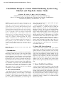
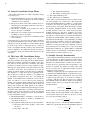
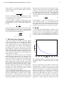
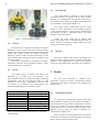
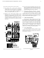
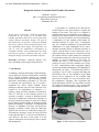
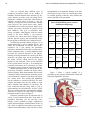
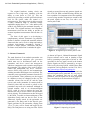
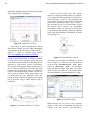
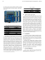
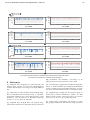
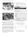
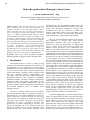
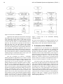
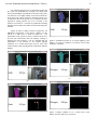
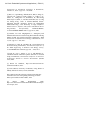
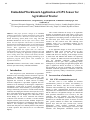
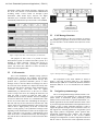
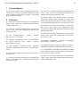
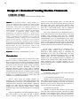
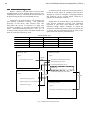
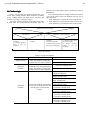
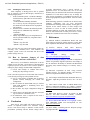
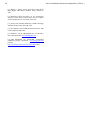
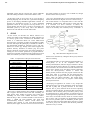
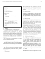
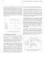
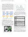
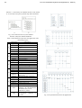
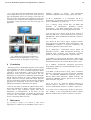
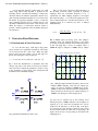
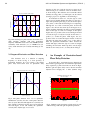
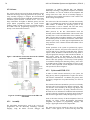
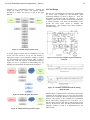
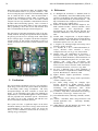
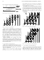
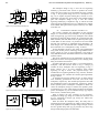
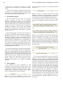
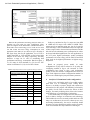
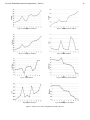
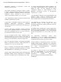
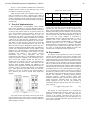
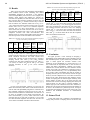
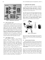
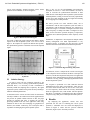
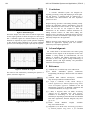
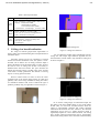
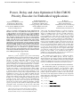
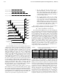
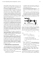
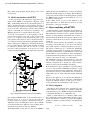
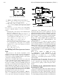
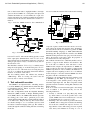
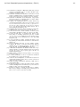
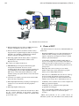
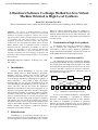
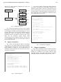
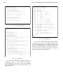
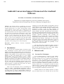
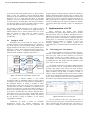
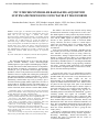
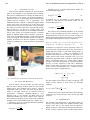
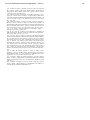
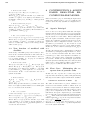
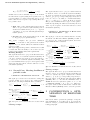
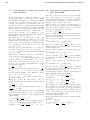
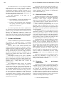
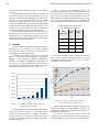
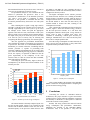
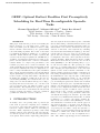
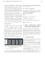
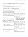
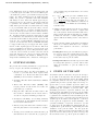
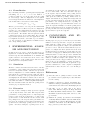
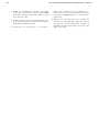
Int'l Conf. Embedded Systems and Applications | ESA'12 | 31 The test and benchmark configuration is as follows: The FX2 module (FX2_TOP_INTERFACE) will clock the external USB chip at 6MHz for Asynchronous transfer USB packet size: 512, 1024, 2048, 4096 and 8192 bytes. Figure 3: Cypress EZ-USB FX2 Development Board Figure 4: EZ-USB FX2 and XUPV5 Interconnected Figure 5: EZ-USB FX2 Benchmarking Tool Figure 4 above shows the USB Development System (EZ-USB FX2) connected to the breakout pins of the FPGA board (XUPV5). Once the USB development board and the FPGA board has been set up correctly, a customized benchmark program is built and run on the client machine to test the throughput of the new USB 2.0 chip using various packet sizes and clock rates. The speed limitations of the USB protocol is dictated by the clock rate supplied as the upper speed limit: 8MHz maximum for asynchronous transfers, 48MHz maximum for synchronous transfers. The max theoretical bandwidth for asynchronous transfers between the USB chip and the FPGA chip is 2 bytes (16-bits) per clock cycle: 16Megabyes/sec constant. The USB Verilog module uses the 48MHz clock line from the EZ-USB FX2 board which is divided by 8 to provide a 6MHz clock for asynchronous USB data transfer. With a 6MHz clock, the maximum throughput is estimated to be 12 Megabytes/sec sustained. 5.2 Connectivity - USB 2.0 Benchmark Summary Figure 6: EZ-USB FX2 Benchmarking Results