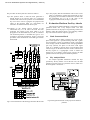
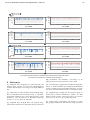
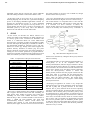
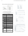
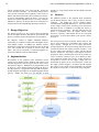
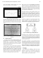
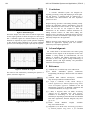
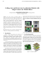
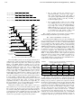
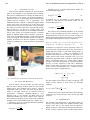
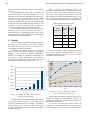
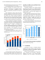
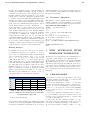
1
Int'l Conf. Embedded Systems and Applications | ESA'12 | SESSION NOVEL APPLICATIONS, ALGORITHMS, SUPPORTING SYSTEMS, AND EMBEDDED DEVICES Chair(s) TBA 1 2 Int'l Conf. Embedded Systems and Applications | ESA'12 | Int'l Conf. Embedded Systems and Applications | ESA'12 | 3 Constellation Design of a Lunar Global Positioning System Using CubeSats and Chip-Scale Atomic Clocks A. Batista1 , E. Gomez1 , H. Qiao1 , and K. E. Schubert1 [email protected], [email protected], [email protected], [email protected] 1 School of Computer Science and Engineering, California State University, San Bernardino 5500 University Parkway, San Bernardino, CA, USA Abstract— Accurate navigation on the moon, Mars, or any other astronomical body is essential to scientific investigation. The research presented in this paper covers the constellation design of a Lunar Global Positioning System (GPS) using the CubeSat platform. Since CubeSats have significantly smaller dimensions than most current satellites, their associated cost is much less to place into orbit. This creates a compelling reason to use them for a Lunar GPS. However, CubeSats require a much smaller atomic clock, which has not been available. Fortunately, there have been recent advancements in chip-scale atomic clocks (CSAC) which can fit within the CubeSat platform. We propose a Rider constellations of two orbital planes and eight satellites per plane for minimum position determination, or fifteen satellites per plane for redundancy at an altitude of 3.34x10⁴ km. The CSAC considered is estimated to have an update interval of almost an hour with a ten meter distance error. Keywords: CubeSat, Chip-Scale Atomic Clock (CSAC), GPS, Lunar, Constellation 1. Introduction Navigation has always been a critical necessity throughout human history. With, the advent of the Global Positioning System (GPS), accurate navigation here on Earth is quickly becoming ubiquitous. As people begin to explore beyond the Earth, navigation will become all the more crucial. Upon the return of people to the moon, navigation will be just as important there as it is here on Earth, not only for exploration on the moon, but also for the astronauts’ safety. GPS allows us to determine our position, velocity, and time (PVT) with a high level of accuracy here on Earth. Therefore, a GPS system on the moon would be just as essential of a system. This research was to provide a first look at a CubeSat constellation for such a lunar GPS. 1.1 The CubeSat Platform The CubeSat platform was designed by California Polytechnic State University, San Luis Obispo, and Stanford University [6]. Their purpose was to develop a pico-satellite (a satellite ≤ 1kg in weight) platform and delivery system that was affordable and standardized, yet robust enough for other colleges and universities to begin satellite and space research programs [6, 7, 8]. A major constraint and challenge of this research is to keep the hardware to a volume that will fit within the CubeSat architecture. CubeSats are currently designed to dimensions of 10 cm3 and 1 kg payload constraint with the maximum size being three modules [7, 8]. Therefore, the largest volume allowed would be 10 cm x 10 cm x 30 cm and up to 1.33 kg. The compelling reason for considering the CubeSat platform is that it is substantially less costly than current GPS satellites and has already been flight tested on many missions. Currently, a GPS satellite costs roughly on the order of magnitude of hundreds of millions to billions of dollars to develop and deploy [12]. This is due to the cost of the atomic clock, size, and weight of the satellite. CubeSats, on the other hand, are on the order of tens of thousands to a few million dollars [13]. 1.2 Lunar GPS System Segments There are three major segments to GPS: space systems, ground control, and the user [1]. First, the space systems segment includes the satellites and their systems. Secondly, the ground control segment includes the ground stations that control, track, and maintain the satellites. Finally, the user segment is the actual GPS receiver and its systems. Another perspective of the segments is that this is the high level design of the GPS system. In this paper, the space systems segment is the only one considered, as the ground control segment and user segment capabilities already exist in many areas. 2. Lunar Satellite Constellation In this section the high level design for the lunar GPS constellation will be shown. Satellite constellations are based upon several factors including the requirements of the system and their orbital parameters. The requirements of the system may include whether constant signal visibility with the satellites are needed. Another could be if worldwide coverage is needed (which it would almost always be). These constraints determine the number of satellites in a constellation and the altitude of their orbits. 4 Int'l Conf. Embedded Systems and Applications | ESA'12 | 2.1 General Constellation Design Theory The general requirements for a GPS constellation design are as follows [1]. 1) For PVT determination at least four satellites must be visible at all times anywhere in the world assuming worldwide access is required. 2) The position offsets of the visible satellites need to be such that there pseudoranges with the receiver are as non-singular as possible. 3) The amount of updates from ground based station needs to be kept to a minimum. 4) There needs to be a balance between orbit altitude and transmitter power for the signal. 5) There needs to be a certain level of redundancy in the event of failures. Considering point 1, one can get away with three satellites if only position determination is necessary. However, considering point 5 as well, the number of visible satellites should be about six [1]. Point 3 is important since if a trajectory needs to be updated, then this requires power and fuel. The fourth is imperative, and additional research will need to be conducted to develop an antenna and transceiver for this subsystem. 2.2 The Lunar GPS Constellation Design Originally, two constellation designs were considered. The first would have been derived from the GPS currently functioning for Earth, specifically the altitude of the satellites. The second was where the constellation and orbital parameters would have been at a lunar synchronous orbit. Although, the orbital altitude of the lunar synchronous orbit would have been ideal, since relativistic errors and the number of required satellites would have been to a minimum, this altitude is too high above the L1 Lagrangian point. This would have caused the satellites to be pulled back by the Earth’s gravitational field. Also, even though the altitude for the Earth-based constellation is below the L1 point, it would be too close to the L1 point, causing the circular orbit to perturb, which would have greatly increased the orbital complexity. This phenomena will be discussed shortly since it affects the orbital altitude of the satellites. The proposed GPS constellation design in this paper uses the aforementioned requirements to govern the specific needs for the lunar system, along with global coverage, and inclined circular orbits. Next, several major factors were determined for the constellation’s design. 1) The minimum number of satellites to cover the moon. 2) The minimum number of satellites to determine the user’s PVT on the moon. 3) The optimized orbital parameters for the constellation. a) The time it takes for the satellite to orbit around the moon. b) The shape of the orbit. c) The altitude and inclination. d) The number of orbital planes to be used. 4) The signal transmitter power. 5) The optimal level of redundancy. First, there is a relation between points one and two where one can be thought of as a subset of two. This is generally because the minimum number of satellites to cover the planet is related to how many are visible at a given time from a specific position on the planet. Since this number is usually less than the minimum number of four visible satellites for GPS, then this is why it is a subset. Next, point three modifies the first two, since those parameters are used to determine the minimum number of satellite coverage. Point four affects 3.3 because the more powerful the transmitter, the higher the satellite altitude can be. Finally, point five is important because although to create redundancy one simply needs to place more satellites or planes in orbit, placing too many extra satellite is not only costly, but if the number of satellites is too large, they can cause a singularity to arise in the pseudorange vectors causing errors to grow in the PVT measurements. Therefore, an optimal number of redundant satellites needs to be calculated. For redundancy, usually six visible satellites is deemed satisfactory [1]. 2.3 Satellite Coverage Determination Since satellites transmit their signals in concentrated bands of energy, direct line of sight is required for signal acquisition to and from the satellites and the receiver. It is obvious that there are a limited number of visible locations where a receiver can be at a given time with correspondence to the position of a satellite. For instance, a receiver at the south pole does not have line of sight with a satellite in position orbiting above the north pole. With line of sight being a pivotal requirement, this is used to determine the minimum number of satellites that need to be orbiting within a given orbital plane in order to have line of sight coverage (from here on out referred to simply as “coverage”). The first step that was employed to calculate this minimum number uses Rider’s method on determining inclined circular orbits [3]. Consider the first equation for the Rider method: cos α cos(θ + α) = (1) 1 + h/r In this equation, θ is the central angle of the body, α is the elevation angle, h is the orbital altitude of the satellites, and r is the radius of the body, in this case the moon. Solving for θ gives the following equation. ) ( cos α −α (2) θ = arccos 1 + h/r The next step is to use θ to calculate the minimum number of satellites for a given plane. Below is the next Rider equation: ( π) cos θ = cos c cos (3) s Int'l Conf. Embedded Systems and Applications | ESA'12 | In this equation, c is a parameter that is defined by Rider as a relation between s and θ [1]. Then solving for s gives the number of satellites. ⌈ ⌉ π ( θ) s= (4) arccos cos cos c The reason for taking the ceiling of this equation is to ensure we get an integer value for the satellites since there cannot be a fractional value of a satellite. Next, the number of satellites for GPS purposes can be determined. First, the orbital altitude of the satellites needs to be determined. In order to do this, Kepler’s third law was used [2]: 4π 2 t2 = (5) r3 Gm For this equation, t is the orbital period, r is the orbital radius, G is the gravitational constant, and m is the mass of the body being orbited. Lastly, solving for r and subtracting the moon’s radius yields the satellite altitude. √ 2 3 Gmt r= (6) 2 4π satalt = r − rmoon (7) 5 developed chip-scale atomic clocks (CSAC) which are about 10 mm3 in volume, and consume only 30 mW [4], making it suitable for an embedded design. In addition, this CSAC has a Allan Deviation less than 1x10⁻¹¹ [4]. Referencing the Galileo GPS specification, and the Allan Deviation the clock validity time can be estimated given a desired distance tolerance [1]: derror (8) t= σy (τ )c In this estimation, σy (τ ) is the Alan Deviation, c is the speed of light in a vacuum, derror is the allowable distance error, and t is the amount of time that can elapse before a clock update needs to be sent to the satellite from the control segment before the distance error grows past its tolerance. 4. Results To determine the minimum number of satellites for the proposed constellation using the Rider method, a program was made to test various orbital altitudes. The graph below shows the results of the minimum number of satellites for coverage on the moon at these altitudes. These results show 3. The Lunar Space Segment The space segment for this GPS is the only segment focused on in this paper. It is worth mentioning that the control segment will be used for sending clock updates for the satellites. There are two major requirements for the space segment. The first is to adhere to the aforementioned constellation design in section 2. The second is to keep the design within the constraints of the CubeSat platform. The major components which contribute to the payload of each satellite would be the electronic and computer hardware, the atomic frequency standard (AFS) clock, the transmitters, the battery, and the solar panels. During the course of this research it was also found that NASA had discovered that there is an ionosphere in the moon’s atmosphere [10]. This discovery dates back as far as the Apollo missions, but had never been qualified until recently by T.J. Stubbs of NASA [10, 11]. It is postulated that the explanation for the lunar ionosphere is from ionized dust particles in the lunar atmosphere [10, 11]. This is important since this ionosphere can have adverse affects on signals sent from orbiting space vehicles down to the lunar surface, producing errors in PVT determination [1]. Assuming the ionosphere is the result of ionized dust particles, it should increase as human exploration expands. Quite possibly the largest hurdle that needed to be overcame was determining a suitable AFS that would fit within a CubeSat. All GPS satellites use an AFS to ensure a reliable clock frequency to reference. However, these are usually large, heavy, and expensive. Recently, there has been much advancement with this technology, and now there has been Fig. 1: Minimum Number of Satellites For Moon Coverage Using Rider’s Method of Inclined Circular Orbits vs Orbital Altitude that as the orbital altitude of the satellites is increased, the minimum number of satellites needed to provide coverage exponentially decays. Once this was determined, the desired altitude was calculated to be 3.34x10⁴ km using Kepler’s third law. This altitude was determined by choosing an orbital period equal to that of one-fourth of a moon day which equals 6.8305 Earth days. Again, it was desired to have the satellites in a lunar synchronous orbit where they would orbit the moon at the same rate it rotates (27.322 Earth Days), or with an orbital period equal to half of the 6 Int'l Conf. Embedded Systems and Applications | ESA'12 | moon’s rotation period similar to that of the Earth’s GPS altitude [9]. However, this would have caused the satellites to have an orbital altitude of 8.7x10⁴ km which is higher than the L1 Lagrangian point (6.3x10⁴ km) for the synchronous orbit which would have caused the satellites to be pulled in by the Earth’s gravity. As for the half moon period orbit, with an altitude of 5.4x10⁴ km the satellites would have been too close to the L1 point causing the orbits to become unstable. Once the altitude was determined, this was used to determine the minimum number of satellites per plane. Referring back to Figure 1, using the calculated altitude the minimum number of satellites to cover the moon would be approximately 2.5 satellites per plane. Now if this design was simply for having coverage by at least one satellite, then taking the ceiling of this would give us three satellites per plane totaling six satellites. In the aforementioned section GPS is shown to require more satellites. Therefore, a minimum coverage of at least three visible satellites anywhere on the moon calculates to 7.5 satellites per plane totaling 15 satellites (Note: One plane would have one less satellite, or to make it even there could be 16 satellites), and a coverage of at least six satellites would be 15 satellites per plane, with 30 satellites in total. Next, using equation (8), the time for update was estimated using the data for the CSAC. Assuming a distance tolerance of ten meters, the time for an update would be over 55 minutes and 30 seconds. This time is a little short, but definitely manageable. If the distance tolerance is extended to 50 and 100 meters, the time for update is a little over approximately 4 hours and 30 minutes, and approximately 9 hours and 15 minutes respectively. 5. Conclusions and Future Directions This paper presented a constellation design for a Lunar GPS using the CubeSat platform incorporating CSACs. This GPS considers a Rider constellations of two orbital planes and eight satellites per plane for minimum position determination, or fifteen satellites per plane for redundancy at an altitude of 3.34x10⁴ km. The CSAC considered is estimated to have an update interval of approximately 55 minutes and 30 seconds for a distance accuracy of 10 m, approximately 4 hours and 30 minutes for a distance accuracy of 50 m, and approximately 9 hours and 15 minutes for a distance accuracy of 100 m. The system is thus feasible, and design costs are well within possible ranges. Future research will include, but not be limited to optimizing the number of satellites in each plane considering areas of zonal coverage, increasing the time between clock updates, transceiver and antenna design, the possible effects of the lunar ionosphere, and improving error measurement. In addition to this proposed system, differential GPS can be incorporated to enhance PVT accuracy. References [1] E. D. Kaplan, C. Hegarty, Understanding GPS: Principles and Applications, 2nd ed., Artech House Publishers, 2005. [2] H. D. Young, R. A. Freedman, Sears and Zemansky’s University Physics, 12th ed., Pearson Addison-Wesley, 2008. [3] L. Rider, “Analytical Design of Satellite Constellations for Zonal Earth Coverage Using Inclined Orbits,” The Journal of the Astronautical Sciences, vol. 34, pp. 31–64, Mar. 1986. [4] J. F. DeNatale, R. L. Borwick, et al, “Compact, Low-Power Chip-Scale Atomic Clock," in Proc. IEEE, 2008, p. 67. [5] R. E. Sorace, V. S. Reinhardt, and S. A. Vaughn, “High-speed digitalto-RF converter,” U.S. Patent 5 668 842, Sept. 16, 1997. [6] (2012) The CubeSat website. [Online]. Available: http://www.cubesat.org/ [7] (Dec. 2010) AMSAT CubeSat Information. [Online]. Available: http://www.amsat.org/amsat-new/satellites/cubesats.php/ [8] J. Puig-Suari, C. Turner, W. Ahlgren, “Development of the Standard CubeSat Deployer and a CubeSat Class PicoSatellite," 2001. [9] (Jan. 2012) NASA Earth’s Moon: Facts and Figures. [Online]. Available: http://solarsystem.nasa.gov/planets/profile.cfm?Object=Moon &Display=Facts/ [10] (Nov. 2011) NASA The Mystery of the Lunar Ionosphere. [Online]. Available: http://science.nasa.gov/science-news/science-atnasa/2011/14nov_lunarionosphere/ [11] T. J. Stubbs, D. A.Glenar, W. M.Farrell, R. R.Vondrak, M. R.Collier, J. S. Halekas, G. T.Delory, “On the role of dust in the lunar ionosphere," Planetary and Space Science, vol. 59, pp. 1659–1664, Oct. 2011. [12] (2004) The James Madison University website. [Online]. Available: http://maic.jmu.edu/sic/gps/satellite.htm [13] (2011) The CubeSat Kit website. Pumpkin Inc. [Online]. Available: http://www.cubesatkit.com/index.html Int'l Conf. Embedded Systems and Applications | ESA'12 | 7 Remote Controlled Terrestrial Robotic Module Alessandro Brawerman, Mauricio Perretto, Felipe Augusto Przysiada Computer Engineering Department, University of Positivo, Curitiba, Parana, Brazil Abstract - This paper presents the development of a low-cost terrestrial robotic module, small dimensions and great autonomy, which allows the user to control it over long distance. The module may be used for investigation in critical environments of difficult access. Communication between the module and the operator is accomplished through an 802.11g network. This communication occurs over a secure protocol that allows encryption of information so that attacks by malicious people on the communication protocol are hampered. A camera captures and transmits images to the operator who can then recognize the surround environment and remote control the module. Keywords: Robotic, hazard terrestrial robotic module 1 environment inspection, Introduction Several robotic applications aim to provide a way of solving tasks in environments that are of difficult access or where there are risks for the human life. Within this scope various options for robotic equipments have been shown to perform tasks in terrestrial, aquatic, mountains, air or even in space. Mobile robots can be grouped into two distinct groups: robots controlled by humans and autonomous robots. The autonomous mobile robots have the ability to move in dynamic and known environments without human control, however, this requires the development of algorithms that allow the definition of their location and movements [1]. Other important set of information about the robotic modules is the features and elements inherent in the design. In [2], the authors present the development of synthetic adhesives for attachment to robots vehicles, allowing them to climb walls and access remote locations that do not allow access through the direct movement to the target. The work in [3] presents the development of robots using an approach to sensor network and multi-agent systems for movement. A particular area for robots application is to perform tasks of preventive or corrective support in critical environments. As shown in [4], the use of robots with long distance control enables the human control and the maintenance process, in the critical environment, without the human presence. For the development of robots in the last case, it is necessary to know the environment in which this will be used and define a number of factors like: size, length, methods of communication between robot and operator, robotic actuators present in the project [5]. The project presented in this paper is to develop a robot with long distance control for preliminary investigation of critical environment for humans. 2 Development This project aims to develop a robotic system with the following characteristics: low-cost, long range, small sized and controlled by humans to perform the inspection tasks in critical environments. The diagram of Figure 1 shows the block interconnection of the developed system. Note that a control block is responsible for receiving information from the sensors and sending them to the actuators. Besides, a mini computer type E-box is responsible for ensuring communication between the control block and the operator and transmitting the images obtained by the camera to the operator. Figure 2 depicts the robotic module prototype. Camera Actuators Control Main Oper ator Sensors Figure 1 – Block diagram of the robotic system Following it will be described each of the blocks developed and communication between them. 2.1 Sensors As an operator controls the developed robotic module, the sensing system contains only a few elements to protect the module from user commands that may provide risk of damage to the module. Tap sensors where attached to the ends to prevent movement against a barrier that is impenetrable, avoiding in this way, the overload of the motors. We also implemented a lightning sensor systems that gets on and off automatically according to the environment. 8 Int'l Conf. Embedded Systems and Applications | ESA'12 | 2.4 Central Module The central module is designed to control the data transmission between the operator and the robotic module. Basically, it is a minicomputer with limited size and capacity. An optimized Linux Kernel was compiled and installed with only the modules required for the application. The central module communicates with the control module via serial communication and the modulus operator via 802.11g WiFi network. A specific port for communication was defined and data is transmitted from/to the central through an encrypted protocol. Figure 2 – Terrestrial Robotic Module 2.2 Actuators The actuators are responsible for handling the module. Furthermore, two servo motors are used to enable the operator to control the camera without the need for displacement of the module. This system provides two degrees of freedom, allowing a vertical axis above and below the display, and the other on the horizontal axis allowing viewing of objects on the side of the module. The motion control module is composed by four motors connected at each end. This configuration allows a greater torque with less power consumption. 2.3 Control 2.5 Command Camera Right Camera Left Move Back Move Front Move Right Move Left Light On Light Off Table 1 - Protocol for communication between Control and Central Module Operador The operator module is the interface that displays and allows the remote control of the robotic module. The modulus operator is a Java application that connects to the robot and receives the transmitted images and captures user commands. 3 The control system of actuators and sensors was performed by a small 8-bit microcontroller. The microcontroller receives the analog and digital signals and communicates with the minicomputer eBox to send commands to the actuators. Communication between these two elements is via RS-232 serial communication. The command handling protocol is presented in Table 1. Letter a b c d e f n o Finally, the central module has an attached USB camera. The camera data is transmitted directly from the central module to the operator through another port using UDP protocol and no encryption. Results The tests were conducted to evaluate system performance in three key features, communication distance between robot and operator, autonomy of the equipment and response time. 3.1 Communication distance To evaluate the communication distance thirty tests were performed in various open and closed environments. It was determined that the maximum communication distance was the one in which the robotic module started to fail to execute commands or to transmit the captured images, rather than the point at which the operator completely lost communication with the robot. Table 3 presents the results obtained for the internal and external tests, tabulating the maximum distance, the minimum distance and the average of the thirty tests. Int'l Conf. Embedded Systems and Applications | ESA'12 | Maximum (meters) Internal 55 External 150 Table 2 - Results distance 3.2 Minimum (meters) 34 100 Average (meters) 50 132 Autonomy The maximum power consumption was calculated as 2.2A, thus to power the robot, two batteries of 6V / 5.2 Ah were employed. According to equation 1, the robotic module autonomy when using maximum consumption is two hours and twenty-five minutes. Aut = Load / consumption In tests conducted in different environments, where the average use was not requiring maximum power the autonomy was extended for up to three hours and thirty minutes using it constantly. 3.3 Response time The objective of this test was to assess the response time between the operator module and the robotic module according to the distance between the two elements. To evaluate the response time of the robotic module ten measurements were performed at varying distances always indoor. Table 4 presents the delay obtained according to the distance. Distance Response (meters) time (ms) 5-15 <100 20 112 25 115 30 122 35 129 40 140 45 148 50 162 Table 3 - Distance x Response The image transmission has reached up to three frames per second, but in most indoor cases the refresh rate was in one frame every three seconds. 9 4 Conclusion This work showed the development of a remote teleoperated robotic module through the 802.11g protocol. The paper presented the development of the whole system platform, including control systems, image capture and transmission protocols defined to ensure a secure communication between the robot and the remote operator. In tests considering the communication distance, similar results to the ones presented in [1,4,5] were obtained. The autonomy of the platform reached values even higher than what was expected for the project, being interesting even to replace the battery pack for only one element of charge. The delay produced in the response time tests is insignificant considering that they were performed on a wireless network in an indoor environment and with a protocol for encrypted communication. The major problem was the transmission time of the image between the robot and the operator, which reached only one image at each trheesecond interval. Finally, currently and future work include the development of a more efficient method of image compression allowing the capture, display and transmission of a greater number of frames per second to the remote operator station. 5 References [1] Sanchez, A.; Hernandez, X. ; Torres, O. ; Alfredo Toriz, P.; Mobile Robots Navigation in Industrial Environments; Mexican International Conference on Computer Science (ENC), 2009 [2] Menon, C. ;Murphy, M. ; Sitti, M.; Gecko Inspired Surface Climbing Robots; IEEE International Conference on Robotics and Biomimetics, 2004. ROBIO 2004. [3] Rodic, A.; Katie, D. ; Mester, G.; Ambient intelligent robot-sensor networks for environmental surveillance and remote sensing; 7th International Symposium on Intelligent Systems and Informatics, 2009. SISY '09. [4] Hamel, W.R.; Murray, P.; Observations concerning Internet-based teleoperations for hazardous environments; IEEE International Conference on Robotics and Automation, 2001. Proceedings 2001 ICRA. [5] Hamel, W.R.; e-maintenance robotics in hazardous environments; IEEE/RSJ International Conference on Intelligent Robots and Systems, 2000. (IROS 2000). Proceedings. 2000 10 Int'l Conf. Embedded Systems and Applications | ESA'12 | Development of an Encryption LSI Resistance Evaluation Platform for Fault Analysis Attacks against the Key Generation Section and Its Evaluation Masaya Yoshikawa, Masato Katsube Department of Information Engineering, Meijo University, Nagoya, Japan Abstract – The algorithm of the advanced encryption standard (AES) has been sufficiently studied to confirm that its decryption is computationally impossible. However, its weakness against fault analysis attacks has been pointed out in recent years. Nonetheless, a method that uses actual large scale integration (LSI) to evaluate resistance against fault analysis attacks has been scarcely reported. This study develops a new resistance evaluation platform for fault analysis attacks against the key generation section of an actual device. Using this platform, the resistance of the actual LSI against fault analysis attacks, which has been uncertain, can be evaluated. Keywords: Hardware security, Fault attack, Encryption LSI, Encryption standard 1 Introduction Confidential information in credit and cash cards is protected against illegal reading through the use of cryptographic circuits. It has been sufficiently confirmed that the decryption of the encryption standards used in cryptographic circuits is computationally impossible. However, it was recently reported that when a theoretically safe encryption algorithm was embedded in the hardware, confidential information could be illegally specified by fault analysis attacks (fault attacks)[1]-[13]. Here, fault attacks specify the secret keys by intentionally generating a fault during the encryption processing and by comparing the fault and normal cases. This study develops an evaluation platform that can verify resistance against fault attacks (tamper resistance) in an actual device through the use of encryption LSI. In the evaluation platform, a fault is generated through a glitch in a clock, which is supplied to the encryption LSI. Based on the results of the encryption processing on which a fault is generated, the fault generation position is specified. This study also develops a new algorithm that will determine whether secret keys can be derived from the fault. The validity of the proposed platform is verified through evaluation experiments performed on an actual device. 2 2.1 Fault Attack Principle of Fault Generation A fault can be generated using three methods: (1) laser irradiation, (2) lowering the power supply voltage, and (3) inserting a glitch in a clock. The method of using laser irradiation is ineffective since it needs circuit information in LSI. Moreover, a laser irradiation apparatus is expensive. The method of lowering the power supply voltage induces an abnormal circuit operation by applying a voltage that is lower than the reference voltage. This method may destroy the circuit since it manipulates the power supply voltage. The method of inserting a glitch in a clock induces data errors by mixing a short clock pulse (glitch) in a clock signal during a specific round of the processing operation. In this process, no possibility of destroying a circuit exists. Therefore, this study adopts the method of inserting a glitch in a clock to generate a fault. In fault attacks using a glitch, a malfunction (fault) is generated by inserting a glitch in a clock signal since the setup time constraint of a flip-flop cannot be satisfied. 2.2 Key Specification in Fault Attack In fault attacks, secret keys are specified using a fault, which has been intentionally generated during the operation of a cryptographic circuit. A pair of cryptograms that contain data errors (cryptogram with the fault) and a correct cryptogram is also used. Previous studies on fault attacks can be roughly classified into (1) attacks against the key generation section (key attacks) and (2) attacks against the cryptographic operation section (intermediate-value attacks). This study investigates the key attacks. During key attacks, when a fault is generated in the key generation section, an intermediate key at the 9th round (9 R) can be obtained using a pair of cryptograms with the fault and a correct cryptogram. In this study, the case where a fault mixed in an intermediate key at 9 R is propagated to an intermediate key at 10 R is examined. Subsequently, the difference between a cryptogram with the fault and a correct cryptogram is obtained. By using the obtained difference and inverse operation of the cryptographic operation section before the AddRoundKey process at 9 R, the key is specified. Int'l Conf. Embedded Systems and Applications | ESA'12 | The procedure of the key attacks is shown as follows: Step1:The position where a fault has been generated is already known (9 R), and two pairs of a cryptogram with the fault mixed in the position of an intermediate key at 9 R and a correct cryptogram are prepared. The values of the mixed-in faults ("e": 0x01-0xFF) are assumed to be different between the two pairs. Step2:Based on the already known position in the intermediate key at 9 R where the fault has been generated, the position of the fault, which is to be propagated to an intermediate key at 10 R, is examined. The examined position is classified into types A to F according to the fault transmission. Figure 1 shows the procedure of the classification of the fault type between 9R and 10R. 11 Step3:The property that the intermediate value m (the correct value) is equivalent to m'(the value with fault) is used. By applying an intermediate formula that correlates with the intermediate key at 9 R to the value of the cryptogram with the fault, the key is specified. 3 Evaluation Platform For Key Attacks The proposed evaluation platform is composed of a fault generation block and a key analysis block. The fault generation block is for the purpose of generating a fault in the hardware while the analysis block is for analyzing whether keys can be derived from an output cryptogram. 3.1 Fault Generation Block This study aims to make a change-over on two out-ofphase clock signals at a specified timing. With this, a glitch can be inserted in a clock at an arbitrary round. Using digital clock manager (DCM) embedded in the field programmable gate array (FPGA), the phase of the basic CLK signal (CLK_A) is shifted to generate basic CLK and phase-shift CLK (CLK_B). On the other hand, the round is counted from the busy signal in a cryptographic circuit to realize the change-over at an arbitrary round. Figure 2 shows the fault generation block of the proposed evaluation platform. 3.2 Key Analysis Block An analysis algorithm determines whether the keys specified by the key attacks can be derived. First, the fault generation position in the key generation section, which is to be investigated, is examined. Fig.1 The classification of the fault type between 9R and 10R Fig.2 Fault generation block of the proposed evaluation platform 12 Int'l Conf. Embedded Systems and Applications | ESA'12 | Tables 1 and 2 show the number of keys that were obtained through the application of key attacks to the key generation section according to the fault diffusion pattern. Table 1 shows the case where the fault diffuses in columns. As shown in this table, the number of specified keys increases as the number of fault generation positions increases. In contrast, as shown in Table 2, despite the increase of the number of fault generation positions, the key still could not be specified. This study investigates the case where the fault generation position in the key generation section diffuses in columns. 4 4.1 Table 2 Case where the fault diffuses in lines Fault position on 9R of Key generation section Evaluation Platform For Key Attacks The number of revealed byte Calculation amount for attack 0bit [N/A] 0bit [N/A] 0bit [N/A] 0bit [N/A] Experiment Outline In the experiments, an AES cryptographic circuit (AES_KL) was designed so that the operation part in the key generation section uses the critical path. In the AES_KL, the SubBytes operation used the conflation method. Verilog was used for the circuit description and it was embedded in the FPGA. Table 1 Case where the fault diffuses in columns Fault position on 9R of Key generation section The number of revealed byte Calculation amount for attack 0bit [N/A] 14 16bit 2 24bit 216 40bit 18 For the embedding, the PlanAhead tool was employed. Logic elements used for the cryptographic operation section were arranged near the section and those used for the operation of the key generation section were dispersedly arranged so that the key generation section uses the critical path. Figure 3 shows the arrangement of the circuit elements of the AES_KL. In the fault generation experiment, a glitch below the critical path was generated to specify the glitch width when data errors occur. The glitch width was either increased or decreased using the signal phase-shift of the DCM parameters. Because of signal skew or deterioration, the phase could not be correctly shifted in the hardware. In the experiment, for a control circuit in which the glitch width was changed, the glitch width was measured five times using an oscilloscope and the average was used. 4.2 2 Fault Generation Experiment In the AES_KL, a path with 0, 8, 16, or 24 bits was lengthened to correspond to the least significant bit (LSB) of the state at the third column in the key generation section. An investigation was then made to determine whether a fault was generated in the lengthened path. Figure 4 shows the experimental results obtained when the glitch width was set to 10.78 [ns]. Int'l Conf. Embedded Systems and Applications | ESA'12 | 13 Fig.4 Relationship between output cryptogram and fault injection position In this figure, the output cryptogram is expressed in 16 1-byte blocks, which are arranged side by side. The byte position in the cryptogram where a fault has been generated is highlighted. When the inverse operation from the fault generation position was performed, a fault was confirmed to be generated in the lengthened path with 0, 8, 16, or 24 bits. Thus, when the critical path was used for the key generation section, a fault was generated in the key generation section and the generated fault was propagated to the cryptogram. 4.3 Fig.3 Result of placement of the circuit elements of the AES_KL Key Derivation Experiment In an experiment using the AES_KL, whether a key could be derived was determined using a cryptogram, where a fault was generated only in the key generation section. In the experiment, the key value was assumed to be unknown. It was also determined whether a key could be derived from the obtained cryptogram. Figure 5 shows the experimental results obtained with the use of the AES_KL. Fault generation bytes were compared using the difference between the output 14 Int'l Conf. Embedded Systems and Applications | ESA'12 | cryptogram with the fault and the correct cryptogram to examine the state in which data errors occurred. Since the fault generation position could not be specified using the obtained cryptogram, the algorithm against the key attacks could not be applied and the key could not be derived. The above-mentioned results indicate that although key attacks are logically efficient, their threads against actual cryptographic circuits are low. [4] Wei Li, Dawu Gu, Yong Wang, Juanru Li, Zhiqiang Liu, "An Extension of Differential Fault Analysis on AES", Proc. of Third International Conference on Network and System Security (NSS), pp.443-446, 2009. [5] P.Maistri, R.Leveugle,"Double-Data-Rate Computation as a Countermeasure against Fault Analysis", IEEE Transactions on Computers, Vol.57, No.11, pp.1528-1539, 2008. [6] Li Yang, K.Ohta, K.Sakiyama, "New Fault-Based SideChannel Attack Using Fault Sensitivity", IEEE Trans. on Information Forensics and Security, Vol.7, Issue 1, Part 1, pp.88-97, 2012. [7] Z.Wang, M.Karpovsky, A.Joshi, "Secure Multipliers Resilient to Strong Fault-Injection Attacks Using Multilinear Arithmetic Codes", IEEE Trans. on Very Large Scale Integration (VLSI) Systems, pp.1-13, 2011. 5 Fig.5 Experimental result of AES_KL on actual LSI [8] H.Li, S.Moore, "Security evaluation at design time against optical fault injection attacks", IEE Proc. on Information Security, Vol.153 , Issue 1, pp.3-11, 2006. Conclusion [9] A.P.Fournaris, "Fault and simple power attack resistant RSA using Montgomery modular multiplication", Proc. of IEEE International Symposium on Circuits and Systems, pp.1875-1878, 2010. This study developed an evaluation platform that could verify the tamper resistance property of fault analysis attacks against an actual device using encryption LSI. Using the proposed platform, a fault could be generated at an arbitrary timing in an actual device. A fault could be generated in the key generation section and it could be determined whether a key could be derived from the generated fault. In the future, we will evaluate resistance when a fault is generated in a cryptographic intermediate value. 6 Acknowledgment This research was supported by Japan Science and Technology Agency (JST), Core Research for Evolutional Science and Technology (CREST). 7 References [1] S.S.Ali, D.Mukhopadhyay, "A Differential Fault Analysis on AES Key Schedule Using Single Fault", Proc. of 2011 Workshop on Fault Diagnosis and Tolerance in Cryptography (FDTC), pp.35-42, 2011. [2] Chong Hee Kim, J.J.Quisquater, "Faults, Injection Methods, and Fault Attacks", IEEE Design & Test of Computers, Vol.24, No.6, pp.544-545, 2007. [3] Gaoli Wang, Shaohui Wang, "Differential Fault Analysis on PRESENT Key Schedule", Proc. of 2010 International Conference on Computational Intelligence and Security (CIS), pp.362-366, 2010. [10] A.Pellegrini, V.Bertacco, T.Austin, "Fault-based attack of RSA authentication", Proc. of Design, Automation & Test in Europe Conference & Exhibition (DATE), pp.855-860, 2010. [11] JeaHoon Park, SangJae Moon, DooHo Choi, YouSung Kang, JaeCheol Ha, "Fault attack for the iterative operation of AES S-Box", Proc. of 5th International Conference on Computer Sciences and Convergence Information Technology, pp.550-555, 2010. [12] A.Barenghi, G.M.Bertoni, L.Breveglieri, M.Pellicioli, G.Pelosi, "Fault attack on AES with single-bit induced faults", Proc. of Sixth International Conference on Information Assurance and Security (IAS), pp.167-172, 2010. [13] K.J.Kulikowski, Wang Zhen, M.G.Karpovsky, "Comparative Analysis of Robust Fault Attack Resistant Architectures for Public and Private Cryptosystems", Proc. of 5th Workshop on Fault Diagnosis and Tolerance in Cryptography, pp.41-50, 2008. Int'l Conf. Embedded Systems and Applications | ESA'12 | 15 Design and Analysis of Academic Dual Chamber Pacemakers Mitchell L. Neilsen Dept. of Computing and Information Sciences Kansas State University Manhattan, KS, USA Abstract In this paper, we describe a relatively inexpensive framework for the design of an academic dual chamber pacemaker that can be used to empirically analyze different pacemaker designs. The goal of this framework is to provide a convenient platform that can be used for research and teaching in realtime embedded system design. The framework can also be used for model-driven development of pacemaker software, and to demonstrate the safety and liveness property violations that may result during the design of real-time pacemaker software. Keywords: Pacemaker, empirical analysis, realtime, embedded system design, medical devices. 1 Introduction A challenge, called the Pacemaker Grand Challenge, was issued by the Software Certification Consortium (SCC). Boston Scientific released the complete system requirements for a fully-functional, previous generation, dual-chamber pacemaker [1]. The goal of releasing this specification was to provide a foundation for future formal methods design challenges, therefore only the basic functions were required to be implemented in hardware; i.e., sensing, pacing and lead impedance measurement. Thus, we will refer to the resulting system as an academic pacemaker. A group of students from the University of Minnesota accepted the challenge to develop a hardware prototype as their senior design project. Based on their design, the Software Quality Research Laboratory, in the Dept. of Computing and Software, at McMaster University developed new hardware evaluation boards using the Microchip 18F4520 PIC processor to control the pacing logic. This hardware prototype, shown as the green board on the right in Figure 1, is used in our framework as well. However, the focus of this paper is on the software framework used for pacing, device control, and management. A pacemaker is a medical device that delivers electrical pulses to the heart muscles to regulate the beating of the heart. The goal is to maintain a sufficient heart rate to compensate for irregularity or blockage in the patient's heart's electrical conduction system. Current pacemakers can be programmed by a cardiologist to select optimal pacing modes for individual patients. In some cases, a cardiologist may use a complex combination of pacemaker and defibrillator in a single implantable device and/or multiple electrodes placed on different positions in contact with the heart. For this framework, only a simple pacemaker with up to two electrodes (one for the ventricle and one for the atrium) are considered. For permanent pacing, the electrodes are placed in a chamber or several chambers of the heart. To simulate the heart, we use software to control a relatively low-cost (~$150 for academic use) 12-Bit, 10 kS/s multi-function Data AcQuisition (DAQ) system from National Instruments, the USB-6008, as shown below in Figure 1. The MicroChip PICkit 2 or PICkit 3 can be used to program and debug the PIC18F4520 chip on the pacemaker board. Both devices can be connected via any available USB ports on any computer. It is very convenient to have the programmer, debugger, data acquisition and signal generation software all conveniently located on a single development system – they are currently all running on a low-end laptop running Windows 7. Figure 1. Basic hardware configuration 16 Int'l Conf. Embedded Systems and Applications | ESA'12 | There are basically three different types of permanent pacemakers based on the number of chambers involved and their basic operation [2]. In a single-chamber pacemaker only one pacing lead is placed into a chamber of the heart, either atrium or ventricle. As shown above in Figure 1, only the ventricle is being paced and sensed in this example setup. However, the system shown above allows both chambers to be paced and sensed. With a dualchamber pacemaker, electrodes are placed in both heart chambers. This type of pacemaker more closely resembles what happens with the natural pacing of the heart. Finally, a rate-responsive pacemaker has sensors that detect changes in the patient's physical activity and automatically adjust the pacing rate to fulfill the body's metabolic needs. On board the pacemaker shown in Figure 1 is an accelerometer that is used to monitor activity, and enable the development of software that is rateresponsive. In a real patient, the pacemaker generator is hermitically sealed with a power source, usually a lithium battery, a sensing amplifier which processes the electrical impulses of the patient's naturally occurring heartbeats as sensed by the heart electrodes, the pacing logic for the pacemaker and the output circuitry which delivers the pacing impulses to the electrodes. These are all embedded in the system shown in Figure 1. Even though the pacemaker will operate on a 9 volt battery, it is more convenient to power it using an external AC adapter. Modern pacemakers have several functions. The most basic pacemaker, monitors the heart's native electrical rhythm. When the pacemaker fails to sense a heartbeat within a normal beat-to-beat time period, it will stimulate the ventricle of the heart with a short low voltage pulse. This sensing and stimulating activity continues on a beat-by-beat basis. The more complex pacemakers also have the ability to sense and/or stimulate both chambers of the heart. The basic ventricular fail-safe pacing mode is VVI or with automatic rate adjustment for exercise VVIR. These are suitable when no synchronization with the atrial beat is required. The wide range of available pacemaker modes is shown in Figure 2. Electronic pacemakers play an important role in society. Several advancements have been made in pacemaker technology over the last fifty years, making current pacemakers highly sophisticated cardiac rhythm managers with thousands of lines of code. They are capable of correcting a wide range of complex heart abnormalities. They can also be easily reprogrammed to accommodate changes in the state of the heart as it ages. However, mode changes must be carefully applied so that they don't interrupt the current operation of the pacemaker. Revise NASPE/BPEG generic code for antibradycardia pacing[3] I II III IV V Chamber(s) paced Chamber(s) sensed Response to sensing Rate modulation Multisite pacing O = None O = None O = None O = None O= None A = Atrium A = Atrium T= Triggered R = Rate modulation A= Atrium V= Ventricle V= Ventricle I= Inhibited V= Ventricle D = Dual (A+V) D = Dual (A+V) D = Dual (T+I) D = Dual (A+V) Figure 2. Pacemaker modes [3] Figure 3 shows a typical example of a pacemaker (pulse generator) hermitically sealed and with leads implanted in the heart. Figure 3. Pacemaker (Pulse Generator) [6] Int'l Conf. Embedded Systems and Applications | ESA'12 | The original hardware sensing circuit was reported to have high noise immunity with the ability to sense down to 37uV [6]. This was achieved by providing a variable gain and reference level for the circuit, under the control of a microprocessor. The pacing circuit is able to provide a nearly continuous range of selectable voltage amplitudes ranging from 1.2 to 7 volts, and the pulse width is only limited by the maximum frequency of the clock. The original hardware lead impedance measurement circuit has the ability to provide an accurate impedance measurement with less than 1% error. The focus of this paper is on developing a complementary software framework. In particular, Section 2 describes a simple and extensible software framework that can be used to design and analyze academic dual-chamber pacemakers. Section 3 provides a simple analysis, verification, and plans for future work, and Section 4 concludes the paper. 17 signals per second, but can only generate signals at a rate of 150 Hz. With our limited testing, this has not been a problem. It is important to have the capability to sense a large number of signals per second so that the paced signals are not lost, even with a very narrow pulse width. Figure 4. NI Signal Express 69mV pulse at 1Hz 2 Software Framework The main functions of an academic pacemaker can be divided into two categories: pace generation which must run in disconnected mode on the pacemaker, and device control and management which are components used to monitor and program the pacemaker. The majority of the code for device control and management, the device controllermonitor (DCM), runs on the PC and communicates with the pacemaker DCM agent via a serial link. The controller passes pacemaker parameters from the PC to the pacemaker. These parameters are also logged in a database as they are changed. In this way, the controller (client) runs on the PC and the agent (server) runs on the pacemaker. In contract, data on electrical pulses that are sensed or pulsed on the pacemaker may need to be monitored. Although an external monitor, such as an electrocardiogram (ECG), could be used to monitor the heart, the monitor here can be used to observe the pacemaker activity directly. This information can also be logged by the DCM. To model an electrocardiogram, a data acquisition (DAQ) card can also be used. In our framework, signals sensed by the pacemaker are generated by the DAQ, and on the flip-side, pace signals generated by the pacemaker, ranging from 1.2 to 7.0 volts, can be sensed and logged by the DAQ. The DAQ that we are using can sense 10,000 As shown in Figure 4, National Instrument's Signal Express software can be used to simulate a heart beat by generating a square pulse of 69 mV at 1 Hz (generated in the top graph, sensed in the bottom graph). Signals can also be generated by an opensource tool built using Python, called Python Data Acquisition Tools (pydaqtools, version 0.2.0, 2011): http://sourceforge.net/projects/pydaqtools/. More accurate representations of the ventricular and atrial signals can be generated. It is very easy to change the amplitude and rate of each signal generated. Also, the signals can be easily logged for more careful analysis as shown below in Figure 5. Figure 5. Output log of signals 18 Int'l Conf. Embedded Systems and Applications | ESA'12 | In this case, the square wave signal representing a heart beat has it's amplitude reduced from 69 mV to 59 mV. Then, as the output log shows, some of the signals are not sensed as heartbeats, and this causes the pacemaker to generate a pacing signal with an amplitude of 3.5 volts. However, with an amplitude of 69 mV, all signals are sensed as shown in the DCM output shown in Figure 6. The data displayed on the DCM in Figure 6 is sent from the DCM agent running on the pacemaker board to the DCM client running on the PC via the serial link. In practice, this serial link would be replaced with a wireless link. This allows a doctor to see what the pacemaker is sensing within the patient. running on the pacemaker board back to the DCM. The pacemaker parameters are also recorded in an EEPROM on the pacemaker board so that it can continue to operate in disconnected mode without intervention from the DCM. The Pulse Generator (PG) on the pacemaker board is responsible for sensing and generating pulsing signals as needed to keep the patient's heart beating. To facilitate automated generation of PG code, we have divided the code running on the pacemaker into two different categories: hardwaredependent and hardware-independent. The Hardware Abstraction Layer (HAL) provides the majority of the code which is not dependent on the particular hardware with a clean interface to the hardware dependent code which consists of device drivers, timers, etc. In this way, we hope to facilitate the automated generation of hardware-independent code from models used to verify the correctness of the pacemaker. Figure 6. DCM real-time ECG output The overall system architecture consists of two major components, the Device Controller-Monitor and the Pulse Generator. The Device ControllerMonitor (DCM) has a graphical user interface with three tabs: Patient Information to specify a patient and retrieve historical data from a database, the current pacemaker configuration is automatically populated in the second tab when a patient's data is loaded. If the patient is new, then system default values are loaded. The Pacemaker Configuration tab allows a cardiologist to select a mode (from those shown in Figure 2). Depending on the mode, a set of configuration parameters can be specified and sent to the pacemaker to reprogram the pacemaker. Once a user connects to a given pacemaker and optionally reprograms the parameters, then real-time ECG data can be transmitted periodically from a DCM agent Figure 7. Pulse generation and sensing using PIC [6] The pulse generator can sense heartbeats, electrical impedance, and acceleration in two dimensions, and it can generate pacing pulses for the ventricle or atrium as shown in Figure 7. The overall software architecture is shown in Figure 8. The Device Controller-Monitor is executed on a laptop and is used to program the pacemaker. On the pacemaker, three real-time tasks are executed. The Pulse Generator runs at the highest priority, the DCM Agent (ECG Transmitter) at the next highest priority, and finally the idle task. These three tasks are executed on top of the FreeRTOS real-time operating system: http://www.freertos.org. The Pulse Generator is responsible for generating electrical pulses as needed to keep the heart Int'l Conf. Embedded Systems and Applications | ESA'12 | operating. Thus, it is the most critical task. The DCM Agent/ECG Transmitter interacts with the DCM Manager to enable a cardiologist to reprogram the pacemaker parameters or select a different pacing mode; e.g., update parameters stored in the EEPROM and passed to the Pulse Generator. It is also used to used to pass real-time ECG data to the DCM Manager. This data is displayed as shown in Figure 6. 19 executed within the framework. In this section, we introduce an abstract model for the VVI mode, which is the fail-safe mode as described in the pacemaker specification. Different modes can be selected by the user from the DCM as shown in Figure 9. To switch to another pacemaker mode, the user only needs to select the new mode from the drop-down list. When the user selects another mode, a new set of parameters are listed for input. Figure 9. Select mode VVI Figure 8. Software architecture The pacemaker is controlled by a Microchip PIC 18F4520 with a limit of 32KB of program memory (flash memory) to store the code to be executed, and even more limiting, only 1536 bytes of data memory (RAM). Because of this, a very limited amount of buffering is done on ECG data. This also limits the number of tasks that can be generated. For example, it might be logical to separate the DCM Agent and ECG Transmitter to run on two separate tasks, but the hardware limits don't allow this many tasks. We plan to consider other processor options and build our own pacemaker board in the future. 3 Analysis of Pacemaker Software A major goal of this new framework is to provide a convenient mechanism to easily compare different abstract pacemaker models, verify the correctness of those models and empirically analyze the designs using the empirical framework described above. At the present, the abstract models are manually converted to C source which is compiled and Note that the mode VVI supports hysteresis and rate smoothing, so the corresponding default values for those parameters are shown, and they may be changed by the user. To program the pacemaker, the user simply needs to click on the button to Connect to the Pacemaker (if they are not already connected), and then click on the Program Pacemaker button to download the parameters to the pacemaker, via the DCM Agent, where they will be stored in EEPROM. The PIC 18F4520 has 256 bytes of EEPROM. Once the new parameters are downloaded, a mode change is initiated, and the new real-time data can be observed. In this case, pacing rate changes are displayed using up and down arrows as shown in Figure 10. Note that even though some heart beats are not sensed, the pace generator may not automatically pace for up to two regular heart cycles. For this example, the signal generated to represent a heart beat is still a square wave with a peak of 59 mV, generated at 60 beats per second. We found that some beats were not detected at 59 mV, but all beats were detected with an amplitude of 69 mV. A variety of different tools can be used to generate input signals with different shapes and 20 Int'l Conf. Embedded Systems and Applications | ESA'12 | amplitudes, including National Instruments' Signal Express, MATLAB, or pydaqtools. Users can also develop their own abstract models for various pacemaker modes. For example, we developed the following model for VVI mode, as shown in Figures 11 and 12. The pacemaker must wait until the Ventricle Response Period (VRP) has passed before generating a pulse. Then, a pulse is only generated if one is not sensed within a given rate interval (RI). Likewise, the pacemaker's environment, in this case the heart can be modeled as an automaton that randomly generates heartbeats in the range from MinDelay to MaxDelay as shown below in Figure 12. Figure 10. Output for VVI mode In the future, we plan to incorporate the Virtual Heart Model (VHM), from Dr. Rahul Mangharam and colleagues at the University of Pennsylvania, to generate a variety of different input signals: www.seas.upenn.edu/~zhihaoj/VHM.html. Another contribution of the framework is to provide a convenient method to illustrate violations of safety and liveness properties discovered using some form of model checking, and the model-driven approach to safety-critical software development. For example, the pacemaker models developed in [7] can be easily converted into code within the Pulse Generator. In [7], the authors show how a transition between VDI and DDD pacing modes can lead to a safety property violation. These pacing modes can be incorporated into the framework. Then, the pacing sequence identified to illustrate the problem can be specified using a simple Python script in pydaqtools. Figure 12. Heart model for ventricle The model can be simulated in UPPAAL as shown below in Figure 13. In this case, system declarations are given by P = Pacemaker(500, 1000, 250), and H = Heart(200, 3000). The pacemaker lower rate interval (LRI) is 500, upper rate interval (URI) is 1000, and VRP is 250, all in milliseconds. The heart MinDelay is 200 and MaxDelay is 3000. Figure 13. Simulator output Figure 11. Pacemaker model for VVI mode Model checking can be used to verify properties among a wide range of distributed and real-time systems. In the past, we have used UPPAAL to Int'l Conf. Embedded Systems and Applications | ESA'12 | 21 verify the correctness of distributed algorithms and real-time schedulers [8,9]. For this model of the VVI mode, a variety of properties can be verified using formal verification. All of the following properties are satisfied for the given model, assuming that the pacemaker and heart are declared with a reasonable set of input parameters; e.g., VRP = 320 msec., etc.: in an indoor lab setting. The system is relatively durable, and can be easily transported between labs. The system can also be used in the classroom to demonstrate more abstract concepts in a concrete fashion. In the future, we plan to port the hardware to a more advanced controller that doesn't suffer from the limitations imposed by the PIC 18F4520. A[ ] ( not deadlock ): check for deadlock freedom, A[ ] ( ( not P.hysteresis and P.WaitBeat ) imply Acknowledgements ( P.y <= P.LRI ) ): the minimum interval between pacing and sensing events is the lower rate interval (LRI) with no hysteresis, A[ ] ( ( P.hysteresis and P.WaitBeat ) imply ( P.y <= P.URI ) ): the minimum interval between events is the upper rate interval with hysteresis, A[ ] ( P.WaitBeat imply ( P.y >= P.VRP ) ) : while waiting for a heart beat, the pacemaker must wait for the ventricle refactory period (VRP) to expire before sensing or pacing, and P.WaitBeat --> P.WaitVRP : being in the state waiting on a heartbeat always leads to being in the state waiting on the VRP to pass. Boston Scientific released the specifications used in this design to promote academic interest in pacemaker technology. Several discussions with Brian Larson were very helpful in completing this initial framework. References [1] [2] [3] 4 Conclusions Biomedical electronic systems are increasing in both complexity and functionality. It is vital to have an understanding of both the human body and the embedded computer software in order to implement functional and reliable systems. This framework is a step in this direction, bridging the gap between biology, electrical and computer engineering and computer science. In this paper, we described a relatively inexpensive, extensible framework that can be used to design new academic pacemakers and analyze existing designs. The goal of this framework is to provide a convenient platform that can be used for research and teaching in real-time embedded system design and verification. In order to design a system, no matter what its purpose, the area of intended use must be researched in order to obtain adequate knowledge to develop a comprehensive system-level understanding of the system. The pacemaker specification includes several advanced features such as telemetry, digital signal processing, and power management. Thus, there are many interesting, well-documented directions to extend this work. Since the pacemaker is used for academic purposes, the primary operating environment will be [4] [5] [6] [7] [8] [9] Boston Scientific, Inc., "PACEMAKER system specification", http://www.cas.mcmaster.ca/sqrl/ SQRLDocuments/PACEMAKER.pdf, 2007. Heart Rythm Society, "Patient information", http://www.hrsonline.org/PatientInfo/, 2011. S. Serge Barold, Roland X. Stroobandt, and Alfons F. Sinnaeve, "Caridiac Pacemakers and Resynchronization Step-byStep: An Illustrated Guide", 2nd Edition, Blackwell Publ., Inc., 2010. John G. Webster, "Design of cardiac pacemakers", IEEE Press, 1995. Richard Barry, "FreeRTOS Reference Manual - API Functions and Configuration Options", Real-Time Engineers, Ltd., 2012. {http://www.freertos.org} C. Nixon, J. Smith, T. Ulrich, R. Davis, C. Larson, and K. Cha, "Academic Dual Chamber Pacemaker", Univ. of Minnesota, Final Report, May 2007. Z. Jiang, M. Pajic, S. Moarref, R. Alur, and R. Mangharam, "Modeling and verification of a dual chamber implantable pacemaker", In Proceedings of the 18th International Conference on Tools and Algorithms for the Construction and Analysis of Systems (TACAS 2012), 2012. M.L. Neilsen, "Model checking task sets with preemption thresholds", in Proceedings of the 17th International Conference on Parallel and Distributed Processing Techniques and Apps. .(PDPTA’11), Paper No. PDP4007, July 2011. M.L. Neilsen, “Symbolic schedulability analysis of task sets with arbitrary deadlines”, in Proceedings of the 16th International Conference on Parallel and Distributed Processing Techniques and Applications (PDPTA’10), Paper No. PDP4851, July 12-14, 2010. 22 Int'l Conf. Embedded Systems and Applications | ESA'12 | 2LGC: An Atomic-Unit Garbage Collection Scheme with a Two-Level List for NAND Flash Storage Sanghyuk Jung and Yong Ho Song Department of Electronics Computer Engineering, Hanyang University, Seoul, Korea Abstract - In NAND flash memory devices, pages marked “invalid” can remain in blocks and occupy flash space. Therefore, it is necessary to physically eliminate invalid pages and collect valid pages from the victim blocks in order to sustain flash write performance and storage lifespan. Although there have been many research studies on efficient garbage collection techniques, research has focused on victim selection methodologies and no solutions have been proposed for the victim selection process cost overhead. Indeed, the host system quite often suffers unendurable storage-access delays because garbage collection produces much computational over-head when doing victim selection. A novel garbage col-lection mechanism, called “Two-Level List-based Garbage Collection”, is proposed in this paper. The victim block selection overhead can be efficiently reduced in this scheme; hence, the responsiveness to host requests is significantly improved. Keywords: flash memory, garbage collection, SSD 1 Introduction There has been a revolutionary change in data storage fields since the development of NAND flash memories. NAND flash memories have been widely used as the storage media of embedded systems such as MP3 players, mobile devices, and digital cameras owing to their non-volatile, high random access performance, and low power consumption flash characteristics. The unit price of flash memory is constantly decreasing because the vendors of flash memories are trying to squeeze more capacity into constantly shrinking silicon dies and adopting multi-level cell (MLC) technology [1]. NAND flash storage devices (i.e., solid state drives) are becoming a viable solution for satisfying the high performance and low power consumption demands of notebooks and desktop-PCs as well as portable embedded systems with continuing improvements in both capacity and price. However, NAND flash memory has several restrictions resulting from its architectural characteristics. First, pages (the minimum data access unit of a flash memory) are designed to share an identical word-line and blocks (consisting of several pages) are designed to share an identical bit-line in order to provide high density memory devices. The unit sizes of the erase and read/write operations are asymmetric for this reason: read/write operations are performed in a page unit while erase operations should be executed in a block unit. Second, electrons in the flash memory data cells can only be removed through an erase operation once the floating gates of the data cells are charged with electrons; thus, the write operation may have to be preceded by an erase operation. This characteristic is sometimes called “erase-before-write”. Third, NAND flash causes an unpredictable electron-leakage problem due to the wearing out of the silicon oxide film which is located between the floating gate and the transistor gate in a cell. The electron-leakage problem mainly causes uncorrectable bit errors and, therefore, the lifespan of flash memory expires after performing a limited number of program/erase (P/E) cycles. In order to hide these constraints of NAND flash memories, current flash-based storage systems use a special interface called a flash translation layer (FTL) [2-5], which is supported by the storage firmware. The main role of the FTL is to make flash storage a virtual in-place updatable storage device. For example, the FTL redirects each write request to the physical flash area and marks the previously programmed page invalid when the host repetitively issues write operations on the same address space. The flash storage can generate a relatively small number of page-copy operations and block-erase operations from this FTL emulation technique, so it is helpful for improving NAND flash memory durability. However, a problem may arise when pages marked “invalid” remain in blocks and occupy flash space. Therefore, it is necessary to physically eliminate invalid pages and collect valid pages from the victim blocks in order to sustain flash write performance and storage lifespan. This sequence of operation processes is called garbage collection [6-7]. The performance and durability of the flash storage can be kept stable if the garbage collection mechanism is efficiently designed. There has been much research [8-15] on efficient garbage collection techniques and various victim block selection methods that cut down on operational overhead have been proposed. However, these research studies have only focused on victim block selection methodologies and have not proposed any solutions for the cost overhead of victim selection processes. Indeed, the host system quite often suffers unendurable storage-access delays because garbage collection produces great computational overhead when performing victim selection processes. Therefore, the storage-access performance and responsiveness of flash storage can be improved by reducing the cost overhead of victim selection processes. Int'l Conf. Embedded Systems and Applications | ESA'12 | A novel garbage collection mechanism known as Two Level list-based Garbage Collection (2LGC) is proposed in this paper. In the proposed scheme, the FTL stores block addresses into two-level lists when the numbers of invalidmarked pages in those blocks pass a threshold. The stacked block map addresses in two-level lists are used for victim selection processes. The FTL can efficiently reduce the victim block selection overhead in this manner; hence, the responsiveness to host requests is significantly improved. Flash storage performance was analyzed using a flash storage prototype platform [16], which consists of hardware parts (i.e., NAND flash controllers, memory controllers, and a CPU) and software parts (i.e., FTL) in order to verify the effectiveness of the 2LGC scheme. The resulting 2LGC scheme offered significant benefits, such as a high performance storage-access ability and a host command delay drop, compared to an on-demand victim search technique in our experiments. The rest of this paper is organized as follows. A preliminary overview of garbage collection mechanisms and latency hiding skills is described in the next section. Related works, including victim block selection techniques and their latencies are reviewed in Section III. The proposed garbage collection scheme is explained in Section IV and its feasibility is discussed. A comparison of the 2LGC scheme to the ondemand victim selection technique in terms of responsiveness is analyzed in Section V. Finally, conclusions are drawn from this study in Section VI. 2 2.1 Preliminaries 2.2 lected victim blocks. However, the FTL should allocate a free block and then copy all the valid pages from victim blocks to the free block because the victim blocks may have valid pages. Consequently, the valid pages scattered over victim blocks are copied to one free block. The FTL updates the mapping information after generating a data block full of valid pages and the victim blocks are then physically erased. The erased blocks are logically located in the free block pool and reallocated when necessary. Latency Hiding of Garbage Collection The storage access frequency of a host system is called data access intensity and is affected by workload characteristics. Storage I/O performance is directly influenced by the factor of data access intensity. During the high data access intensity, the host event queue can be filled with storageaccess requests and hence must be handled immediately. On the other hand, during the low data access intensity, the storage system becomes largely idle and its bandwidth is greatly under-utilized [17]. Therefore, a large portion of the run-time garbage collection cost can be saved if the FTL implements time-consuming operations during low data access intensity. However, the request-pending problem must be considered when adopting an idle-time garbage collection technique. The FTL should suspend garbage collection and immediately back into the request handling process when the host issues storage-access requests during low data access intensity. Therefore, the responsiveness to the host storage-access requests can be improved if the garbage collection operations are preemptively designed. Garbage Collection Mechanism The FTL address re-mapping technique has a problem in that invalid-marked pages occupy the flash area without being erased. If these invalid-marked pages accumulate in the flash storage, the problem of no more available free blocks arises, although the capacity of used space is much smaller than that of the flash storage. Therefore, it is necessary to physically eliminate invalid-marked pages and make free blocks available in order to sustain flash write performance and storage capacity. Garbage collection is thus needed for reclaiming invalid-marked pages scattered over blocks so that the invalid-marked pages can again become free pages. The garbage collection sequence and its operational cost are summarized as follows. 23 The FTL selects some blocks which are expected to have the lowest garbage collection cost as victim blocks when garbage collection is triggered. The P/E cycles or hot/cold identification of each block as well as the number of invalid pages can be considered when selecting victim blocks. The FTL targets entire blocks as victimcandidate blocks of flash storage, which may cause a serious operational cost. The FTL implements block erase operations in order to physically remove the invalid-marked pages from the se- 3 Related Works In this section, victim block selection techniques of garbage collection are analyzed and an explanation is given for the operational latencies incurred by those techniques. 3.1 Victim Block Selection Various cost-based garbage collection techniques [6-15] have been proposed over the past several years. In the Greedy algorithm, Wu et al. [8] first suggested that the FTL selects blocks having the largest number of invalid-marked pages as victim blocks. In this way, the FTL can reduce the number of page program operations from victim blocks and improve the performance and durability of NAND flash storage. However, the subsequently proposed algorithms, such as the Costbenefit scheme [9], indicate a problem in that the Greedy algorithm is not suitable for prolonging the lifespan of flash storage because the Greedy algorithm selects victim blocks without considering their P/E cycles. Therefore, many subsequent studies [10-15] have proposed victim block selection techniques considering wear leveling costs. However, the dynamic wear leveling and static wear leveling schemes [18-19] have already been adopted inside flash storages, so there is no need to consider both 24 Int'l Conf. Embedded Systems and Applications | ESA'12 | wear leveling and garbage collection issues together. Consequently, if the wear leveling cost is not taken into consideration, the Greedy algorithm shows the highest performance in terms of garbage collection cost compared with other victim selection techniques. 3.2 Victim Selection Latency Measuring computational latencies from garbage collection is a totally different issue because the previously published research on garbage collection schemes did not focus on victim block management costs such as victim selection overheads and sorting delays. Thus, victim block management costs must be carefully analyzed in order to decrease garbage collection latencies. The garbage collection operational delays, based on previous research, are as follows. First, the FTL extracts the number of invalid-marked pages from each block by searching the entire flash memory space. Extracting the number of invalid-marked pages will take longer for larger capacity flash storage because flash storage has the same number of block map entries as the number of data blocks. Second, the FTL continuously compares the number of invalid-marked pages from each block until enough victim blocks are selected in order to select victim blocks having the largest number of invalid-marked pages for each block. Although it is assumed that the FTL uses a quick sort algorithm which has the best performing speed among the well-known sorting algorithms, the operational delay becomes O(NlogN) in general case, and O(N2) in the worst case. 4 4.1 structure for supporting garbage collection or wear leveling algorithms. 2LGC Victim Block Selection The 2LGC scheme is able to isolate victim block selection from garbage collection. In short, this scheme maintains the victim priority of target blocks by sorting the blocks by the number of invalid-marked pages during run-time. The two-level lists are used to implement the run-time victim block searching technique, as shown in Figure 4: a candidate list and a garbage block list (along with other de-tails that are explained in Section IV (C)). In the 2LGC scheme, the FTL stores physical block addresses in the two-level lists depending on the numbers of invalid-marked pages and uses them when necessary. This allows the flash storage to reduce block searching overheads and victim block sorting costs during garbage collection. Figure 1 rep-resents the controller architecture of a NAND flash storage and the location of the 2Llist. Figure 2 shows the 2LGC map entries. First, the page map table is an essential data structure of a page mapping FTL. The main role of this table is to translate logical page numbers (LPNs) from a host system into physical page numbers (PPNs) in NAND flash memories. Second, the aim of the block map table is to store physical block information whether the block is available or not when the FTL allocates free blocks. The block map table is also an essential data Fig. 1. Flash storage controller architecture. Fig. 2. 2LGC map entries: (a) page map entry and (b) block map entry. As shown in Figure 2(a), each page map table entry is composed of a 31-bit PPN and a 1-bit page validation-mark flag. The number of entries in a page map table is the same as the number of pages in the flash storage. If the storage access request from the host is issued to the flash storage, the FTL searches the 31-bit PPNs of the page map table using the LPNs (if a physical page size of 8KB is assumed, the 31-bit page number can represent 244 bytes or 16TB). On the other hand, the FTL has to check the page validation-mark flag using the PPNs in order to confirm whether or not the data in physical page space are valid. The address space can be more efficiently saved by combining a 31-bit PPN and a 1-bit page validation-mark flag into a single 32-bit I/O bus width register. There are six entries in the block map table as shown in Figure 2(b). The usage of each entry is as follows. First, 2LGC uses three flags for supporting address translation. A 1-bit bad block-mark flag, a 1-bit free-mark flag, and a 1-bit erase-mark flag represent whether the physical block is bad or not, free or not, and erased or not, respectively. Second, 2LGC uses two page offset entries for maintaining page information within a block. An 8-bit invPage offset shows how many invalid pages are involved within a block and an 8-bit curPage offset explains which page of the block is available for programming. Lastly, the 13-bit eCount number stands for the number of times each block has been erased. 4.2 Single-Block Garbage Collection The FTL selects multiple victim blocks, copies valid pages into one free block, and invalidates the victim blocks in the on-demand victim selection techniques. For example, the Int'l Conf. Embedded Systems and Applications | ESA'12 | FTL updates the page map table with a new physical page number and erases victim blocks whose physical block numbers are 2, 4, and 5 when page copy operations are finished, as shown in Figure 3(a). The FTL needs to copy four pages and erase three blocks as well as to search victim blocks and update map tables during this multiple-block garbage collection process. As seen in this example, the on-demand victim selection techniques can make relatively more reusable free blocks, but may cause a large peak delays within only one garbage collection 25 (1) If the Candidate list is full, a block whose entire pages are invalid is demoted into the Garbage block list. If user workloads, such as file copies and internet explorations, are used, several blocks can be expected to be demoted into the Garbage block list because they include a large number of sequential program operations. However, if the Candidate list does not have such blocks any more, the 2LGC sorts the blocks of the Candidate list in the order of invalid-marked page numbers and removes a block address from the tail of Candidate list. The block address currently being added to the Candidate list is quickly demoted to the Garbage block list if pages in the block are sequentially programmed. (2) When garbage collection is triggered, the 2LGC firstly checks the Garbage block list and selects a block from the head of the Garbage block list as the victim. If the Garbage block list is empty, the 2LGC then checks the Candidate list and selects a block from the head of the Candidate list. Fig. 3. (a) An existing garbage collection and (b) 2LGC mechanism. On the other hand, the 2LGC scheme can separate a garbage collection sequence into several single-block garbage collection operations, so it is possible to improve responsiveness and make the flash storage preemptive. Note that the 2LGC can implement single-block garbage collection mainly because the FTL can use a page offset for each block stored in the curPage offset entries, as shown in Figure 2(b). All the blocks can be reallocated as non-free states through the use of curPage offsets. For example, as shown in Figure 3(b), the FTL updates the page map table with a new physical page number and erases the block whose physical block number is 5 when page copy operations are finished. In this case, the FTL needs to copy two pages and erase one block and update the map tables during the single-block garbage collection process. Compared with on-demand victim selection mechanisms, 2LGC single-block garbage collection is quite effective for supporting a preemptive storage system 4.3 Algorithm Figure 4 shows the two-level lists used in the 2LGC algorithm. The operational sequence is as follows. The FTL continuously checks the number of invalid-marked pages for the corresponding block whenever the page validation-mark flag of each page map entry is updated. If the number of invalid-marked pages in that block is over a threshold value, the 2LGC stores the block address in the Candidate list. The entries in Candidate list are not to be sorted in the initial state. The 2LGC can reconstruct the Candidate list only when the following two cases occur. Fig. 4. Two-level lists in the 2LGC algorithm In 2LGC, the FTL is designed to use a single-block garbage collection scheme, as mentioned in Section IV (B). Although the host issues storage-access requests during garbage collection, the FTL can back into the request handling process without putting a bookmark in the garbage collection sequence because the block addresses already exist in the Candidate list. In the same way, background garbage collection can be implemented atomically. The 2LGC has only to add the block address to the Garbage block list when finishing background single-block garbage collection. 5 5.1 Experiments Performance Evaluation In order to verify the effectiveness of 2LGC scheme, we conducted real-system based experiments using a flash prototype platform board [16] equipped with an INDILINX barefoot SSD controller. The SSD controller of the platform board consists of hardware parts (i.e., NAND flash controllers [20], memory controllers, and a CPU) and software parts (i.e., FTL), so an algorithmic evaluation can be performed by redesigning the firmware inside the SSD controller. Moreover, the most accurate and reliable experiments can be conducted through this platform because the platform board is connected 26 Int'l Conf. Embedded Systems and Applications | ESA'12 | by a SATA2 interface using a notebook or desktop as storage [21]. The platform board and the specification of INDILINX barefoot SSD controller are shown in Figure 5 and Table 1, respectively. Table 2. Workloads 5.2 Fig. 5. Flash prototype platform board. Table 1. SSD controller specification of platform board Figure 6 shows the flash storage IOPS varied with the garbage collection scheme during the time intervals. In this experiment, the IOPS represents the number of page-level commands generated by the FTL, not the number of requestlevel commands issued by the host. The IOPS of the 2LGC scheme were compared to that of the on-demand victim selection technique using the IOMeter benchmark workloads shown in Table 2. As shown in the figure, the average IOPS of the 2LGC scheme is superior to that of the on-demand victim selection technique because 2LGC saves garbage collection costs. There is a significant decrease in the IOPS of the on-demand victim selection technique because it causes entire block searching and victim selection overhead when garbage collection is triggered (see Section III (B) for more details of garbage collection latency). On the other hand, the 2LGC scheme can reduce the system latencies caused by garbage collection because it maintains victim-candidate blocks within the two-level lists during system run-time. Moreover, the peak delays can be minimized and responsiveness to the host improved because of the effectiveness of the single-block garbage collection technique. 6 The IOMeter benchmark [22] is used for generating meaningful workloads in the experiments. In order to extract the accurate experimental data, we exclude data I/Os caused by operating systems or file systems. The platform board is connected to the host as flash storage without installing any operating systems or formatting any file systems because the IOMeter benchmark can handle direct storage-access operations to the unformatted data storage. The IOMeter benchmark can also organize workloads of various read/write and random/sequential access intensities; thus, configurable workloads with the desired properties can be generated. The workload variation is shown in Table 2 (the minimum storage access unit size is 32KB due to the page clustering technique). Finally, the flash storage is programmed with a random/sequential write ratio (r: 50/ s: 50) for aging entire pages to enable the measurement of garbage collection operation latencies. In this experiment, the threshold value is defined as 3/4 of the number of pages in a block, the Candidate list size is 1/20 of storage capacity, and the Garbage block list size is 1/10 of storage capacity, respectively. IOPS and Execution Time Conclusion In this paper, we have studied the operational mechanisms and the computational overheads of garbage collection. The garbage collection was found to have too much computational overhead to find victim blocks, resulting in unendurable host system access latency (very low responsiveness) and performance degradation. However, the proposed 2LGC garbage collection scheme eliminated the computational overheads due to victim block selection from the critical path of the garbage collection operations. The responsiveness to host system requests was also improved by making the garbage collection operation preemptive. The 2LGC scheme achieved significant performance improvement in flash storage bandwidth and request processing latency in comparison to the on-demand victim selection technique in our experiments. 7 Acknowledgement This work was supported by the National Research Foundation of Korea (NRF) grant funded by the Korea government (MEST) (No. 2011-0017147). 27 1200 1200 900 900 IOPS IOPS Int'l Conf. Embedded Systems and Applications | ESA'12 | 600 0 0 100 150 200 2500 2000 1500 1000 500 0 0 50 100 150 600 600 400 400 200 0 50 100 150 200 0 50 100 150 200 0 50 100 150 200 0 50 100 150 200 2500 2000 1500 1000 500 0 200 IOPS IOPS 50 IOPS IOPS 0 200 0 0 0 50 100 150 200 1000 800 600 400 200 0 IOPS IOPS 600 300 300 0 50 100 150 200 1000 800 600 400 200 0 Fig. 6. IOPS comparison between the on-demand victim selection scheme and the 2LGC scheme, (a) workload 1, (b) workload 2, (c) workload 3, and (d) workload 4. 8 References high performance and durability,” Proceedings of the IEEE/ACM International Conference on DAC, 2009. [1] Sanghyuk Jung, Sangyong Lee, Hoeseung Jung, and Yong Ho Song, “In-page error correction code management for MLC flahs storages,” Proceedings of the IEEE MWSCAS, 2011. [4] Aayush Gupta, Youngjae Kim, and Bhuvan Urgaonkar, “DFTL: A flash translation layer employing demand-based se-lective caching of page-level address mappings,” Proceedings of the ACM International Conference on ASPLOS, 2009. [2] Sang-Won Lee, Dong-Joo Park, Tae-Sun Chung, DongHo Lee, Sang-Won Park, and Ha-Joo Song, “A log bufferbased flash translation layer using fully-associative sector translation,” ACM Transactions on Embedded Computing Systems, vol. 6, no.3, article 18, July 2007. [5] Sanghyuk Jung, Yangsup Lee, and Yong Ho Song, “A process-aware hot/cold identification scheme for flash memory storage systems,” IEEE Transactions on Consumer Electronics, vol. 56, no. 2, pp. 339-347, May 2010. [3] Sanghyuk Jung, Jin Hyuk Kim, and Yong Ho Song, “Hierarchical architecture of flash-based storage systems for [6] Li-Pin Chang, Tei-Wei Kuo, and Shi-Wu Lo, “Realtime garbage collection for flash-memory storage systems of 28 real-time embedded systems,” ACM Transactions on Embedded Computing Systems, vol. 3, no. 4, November 2004. [7] Ohhoon Kwon, Kern Koh, Jaewoo Lee, Hyokyung Hahn, “FeGC: An efficient garbage collection scheme for flash memory based storage systems,” The Journal of Systems and Software, pp. 1507-1523, 2011. [8] Wu, M., Zwaenepoel, W., “eNVy: a non-volatile, main memory storage system,” Proceedings of the ACM International Conference on ASPLOS, 1994. [9] Kawaguchi, A., Nishioka, S., Motoda, H., “A flashmemory based file system,” Proceedings of USENIX Technical Conference, 1995. [10] Chiang, M., Lee, P.C.H., Chang, R., “Cleaning algorithms in mobile computers using flash memory,” Journal of Systems and Software, 1999. [11] Kim, H., Lee, S., “A new flash memory management for flash storage system,” Proceedings of the COMPSAC, 1999. [12] Manning, C., Wookey, “YAFFS Specification,” Aleph One Limited, 2001. [13] M-Systems, “TrueFFS Wear-Leveling Mechanism.” [14] Chang, L., “On efficient wear leveling for large-scale flash-memory storage systems,” Proceedings of the ACM SAC, 2007. Int'l Conf. Embedded Systems and Applications | ESA'12 | [15] Du, Y., Cai, M., Dong, J., “Adaptive garbage collection mechanism for N-log block flash memory storage systems,” Proceedings of the ICAT, 2006. [16] http://www.openssdproject.org/wiki/The_OpenSSD_Project. [17] Yangsup Lee, Sanghyuk Jung, and Yong Ho Song, “FRA: A flash-aware redundancy array of flash storage devices,” Proceedings of the CODES+ISSS, 2009. [18] Yuan-Hao Chang, Jen-Wei Hsieh, and Tei-Wei Kuo, “Endurance enhancement of flash-memory storage systems: An efficient static wear leveling design,” Proceedings of the IEEE/ACM International Conference on DAC, 2007. [19] Li-Pin Chang and Chun-Da Du, “Design and implementation of an efficient wear-leveling algorithm for solid-statedisk microcontrollers,” ACM Transactions on Design Automation of Electronic Systems, vol. 15, no. 1, December 2009. [20] Samsung Datasheet. flash memory Spec, K9LCG08U1A, [21] Technical Committee T13 AT Attachment, “Information Technology – ATA/ATAPI Command Set – 2 (ACS-2),” T13/2015-D, Revision 2, August 3, 2009. [22] http://www.iometer.org/ Int'l Conf. Embedded Systems and Applications | ESA'12 | 29 Fast Prototyping of an Image Encoder using FPGA with USB Interfacing Airs Lin1, Evan Tsai1, Gabriel Nunez1, Gregory Carter1 Neil Arellano , Jorge Estrada1, Adrienne Lam1, Sergio Mendoza1, Aleksander Milshteyn1 Dr. Helen Boussalis1, Dr. Charles Liu1 1 Structures, Propulsion and Control Engineering University Research Center (SPACE URC) California State University, Los Angeles 5151 State University Drive, Los Angeles, CA 90032 1 Abstract — This paper focuses on porting specific ubiquitous computing applications by providing acceleration for a Semantic Information System (SIS) [1]. The necessary connectivity protocol for multimedia data transfer on a Field Programmable Gate Array (FPGA) chip via USB has been fully implemented. The SIS network applications that were designed by the CSULA SPACE Center1 are geared towards providing education-oriented users with a real-time virtual environment that allows collaboration in conjunction with distant communication and interaction. The SIS includes applications for its network participants, such as the multicasting Ubiquitous Video Conferencing, the Scraping Tool for metadata processing, multi-touch user interface, etc. However, the power consumption and computing resources of the client system can be in heavy demand by the SIS participants due to real-time video decompression and compression, respectively. The proposed approach can help by conserving the client’s resources, which can lead to an acceleration of SIS functionalities. KeywordsUbiquitous, Conferencing. 1 FPGA, connectivity, Semantic, Introduction The Advanced Computation and Communication (ACC) team of the NASA-CSULA SPACE Center is focused on design and development of new tools for information dissemination for collaborative education and research1. The SPACE Center consists of faculty-led graduate and undergraduate students, which are formed into specific teams based on particular areas of research. The current project objective is to design and implement an FPGA-based image processor as an embedded system that is able to run certain SIS applications with minimal client computer processing. It will initially serve as a modular device via rapid prototyping, which provides acceleration to a client machine by offloading specific functions of SIS applications. Example, such as, real-time compression is done by utilizing a JPEG encoder to eventually leverage towards motion JPEG for video streams. 1 Acknowledgement to NASA University Research Center Program, Grant # NNX08BA44A 2 Semantic Information System Network and UVC Overview The SIS Network is intended to target communities with similar interests, whether that collective is in industry, education facilities, or for recreational purposes. Combined with Ubiquitous Video Conferencing, the SIS framework is designed with flexible GUI (Graphical User Interface) controls for a wide range of uses to accommodate a broader range of audiences. In order to transport video information between UVC participants, a video codec is required. The UVC application utilizes the Motion-JPEG algorithm [2] for video encoding and decoding, where JPEG encoding is the first step. JPEG is a lossy image compression standard named after its creators, the Joint Photographic Experts Group [3]. 3 Integration to the UVC System / Data Processing Certain SIS applications running on the client machine will send the uncompressed data to the FPGA, which in turn, will send the compressed data back to the PC for concatenation and header processing using a high speed communication link. A Field Programmable Gate Array (FPGA) is a reprogrammable logic chip that provides the ability for realtime parallel processing that increases computational performance, ease of hardware scalability, fast prototyping, and reconfigurability of its hardware fabric to change to any computational algorithms that are desired. 30 Int'l Conf. Embedded Systems and Applications | ESA'12 | Xilinx Virtex-5 XC5VLX110T 10/100/1000 tri-speed Ethernet USB host/peripheral controller (Cypress CY7C67300) 4 FPGA Data Connectivity There are two ways to connect the FPGA to the SIS network: Ethernet can be connected to a LAN for ease-of-use in terms of functionality sharing among clients, or by using the USB 2.0 protocol, which requires a client PC to connect to the SIS network. The USB 2.0 protocol supports three speed ratings [6]: 1) low-speed Figure 1: Software Vs Hardware Processing Figure 1 above shows hardware advantages over software in terms of clock cycles needed to perform certain calculations. The ability of parallel processing makes FPGAs the preferred choice for time-sensitive applications that are computationally intensive. [4]. (USB 1.0) rate of 1.5 Mbit/s (~183 kB/s) 2) full-speed (USB 1.1) rate of 12 Mbit/s (~1.43 MB/s) 3) high-speed (USB 2.0) rate of 480 Mbit/s (~57 MB/s) The USB 2.0 protocol will initially be used for multimedia streaming purposes, particularly using one of the specific USB transfer protocols. In the USB 2.0 protocol, there are four types of data transfer modes but only one will be mainly used: Bulk Transfer Mode: This transfer mode is used by mass storage devices for any amount of non-time sensitive data transfer. This transfer mode guarantees data delivery only. 5 Figure 2: Overall System State Machine Diagram Figure 2 above shows an overall project state machine diagram of the system that drives the Verilog modules within the FPGA, as well as the software tasks on the computer side. The application that will run within the computer is responsible for converting and sending the raw pixel values, as well as receiving the output bitstreams from the FPGA to be reassembled into a final compressed JPEG image via the USB protocol 3.1 Embedded Hardware Specifications The FPGA hardware used for this project is a Xilinx XUPV5-LV110T Development System [5], which has been prepared by the Xilinx University Programs for educationaluse. The development board offers the following key features which are necessary for the project: Project Developments When implementing a MJPEG codec, it is necessary to visualize its process as a series of sequential JPEG images being rendered at high speed. An open-source JPEG Encoder [7] written in Verilog will be used since its internal processing does not rely on any proprietary code or license. This particular encoder does not perform any sub-sampling of the final image data, which makes the processed output bitstream larger (4:4:4 color space) than the preferred 4:2:0 color space. The reduction of the color space effectively reduces overall size by half with little discernable visual deficiency. 5.1 Connectivity - USB 2.0 Testing According to the datasheet of CY7C67300 from Cypress, the USB chip included on the FPGA board only meets the USB 2.0 specification requirements for supporting USB 1.0/1.1 speeds, as USB 2.0 high speed is not actually supported. Therefore, the maximum burst throughput of CY7C67300 on the board is approximately 1 Megabytes per second (USB 1.1), so an alternative method is to integrate an external USB development board (Cypress EZ-USB FX2) [8] to provide the necessary connectivity bridge at full bandwidth between the client machine and the FPGA board. Int'l Conf. Embedded Systems and Applications | ESA'12 | 31 The test and benchmark configuration is as follows: The FX2 module (FX2_TOP_INTERFACE) will clock the external USB chip at 6MHz for Asynchronous transfer USB packet size: 512, 1024, 2048, 4096 and 8192 bytes. Figure 3: Cypress EZ-USB FX2 Development Board Figure 4: EZ-USB FX2 and XUPV5 Interconnected Figure 5: EZ-USB FX2 Benchmarking Tool Figure 4 above shows the USB Development System (EZ-USB FX2) connected to the breakout pins of the FPGA board (XUPV5). Once the USB development board and the FPGA board has been set up correctly, a customized benchmark program is built and run on the client machine to test the throughput of the new USB 2.0 chip using various packet sizes and clock rates. The speed limitations of the USB protocol is dictated by the clock rate supplied as the upper speed limit: 8MHz maximum for asynchronous transfers, 48MHz maximum for synchronous transfers. The max theoretical bandwidth for asynchronous transfers between the USB chip and the FPGA chip is 2 bytes (16-bits) per clock cycle: 16Megabyes/sec constant. The USB Verilog module uses the 48MHz clock line from the EZ-USB FX2 board which is divided by 8 to provide a 6MHz clock for asynchronous USB data transfer. With a 6MHz clock, the maximum throughput is estimated to be 12 Megabytes/sec sustained. 5.2 Connectivity - USB 2.0 Benchmark Summary Figure 6: EZ-USB FX2 Benchmarking Results 32 Int'l Conf. Embedded Systems and Applications | ESA'12 | Figures 5 and 6 shows the throughput tests and results of the external USB controller using only a 6MHz clock, which in this case, tops out at approximately 10 Megabytes/sec. Figure 7: Completed Verilog Modules to be used Now that the FPGA has a way to transport data between itself and the host computer, additional modules are required (interconnecting modules) to pass data between the USB module and the JPEG encoder, which are shown in the figure above. 5.3 5.4 Developing module the ‘’beginning’ interconnecting The initial problem is the differences in the amount of data per clock between the USB interfacing module ‘USB_FX2_Control’ and the JPEG Encoder module ‘JPEG_ENC’, as well as the formatting of said data. In order to correctly format the input and output data, interconnecting modules are built which are internally called ‘JPEG_IF’ (USB-to-JPEG Encoder Interfacing) and ‘Combine_final_data’ (JPEG Encoder Output-to-USB Interfacing). The main details of the ‘USB_FX2_Control’ is that the module inputs and outputs data at 16-bits per clock within a shared bi-directional bus. The main details of the inputs/outputs of the ‘JPEG Encoder’ is the 24-bits of input data per clock (8-bit values per color per pixel). The output is 32-bits of processed JPEG bitstream, asynchronous and 7-bits total of end-process control data. Planning and Developing the Interconnecting Modules Figure 9: Planning State Machine for ‘beginning’ Interface (JPEG_USB_IF) Figure 8: Top-level Module Connection Diagram Figure 8 above shows the top-level module connection diagram of the entire project, which includes the ‘beginning’ and ‘ending’ interconnection modules. In Figure 8, the ‘initial’ interconnecting module (colored in yellow) has been tested and verified of its output data towards the JPEG Encoder by reinterpreting the included testbench from the encoder. The next step is to plan, build and finalize the ‘ending’ interconnecting module (‘Combine_final_data’ in red) so that the ‘USB_FX2_Control’ module is able to accept the output data and send it to the host computer. Once all Verilog modules are completed, software development on the PC will commence which is tasked to send raw pixel data over the USB protocol and onto the FPGA device itself, as well as re-concatenate the output data from the device with the necessary header data to finally form a compliant and readable JPEG image file. The reason for an internal buffer within ‘JPEG_IF’ (shown in Figure 9) is to correctly align the incoming 16-bits of data from the USB module into the 24-bits of data that the JPEG encoder module requires. For the first 16-bits coming from the USB module, it holds only 2/3 of the 1st pixel data, then the second 16-bits of input data contains the last 1/3 of the 1st pixel data, and the first 1/3 of the 2nd pixel data, so on and so forth. The buffer size is appropriately sized in terms of being the least common denominator (of 16 and 24 bits), so data going into/from this internal buffer will not have any skewed/unaligned outputs or inputs, which greatly decreases code complexity. Therefore, the module uses 3 clocks of 16bit data in order to output 2 clocks of 24-bit data into the JPEG encoder and continue to do so until the end of the raw pixel input. Int'l Conf. Embedded Systems and Applications | ESA'12 | 5.5 Developing the ‘ending’ interconnecting module The purpose of the ‘Combine_final_data’ module is to format the data output of the ‘JPEG_ENC’ into a suitable format that the ‘USB_IF’ module can use to send it back to the host computer. The input data to this module is a 32-bit JPEG_bitstream that is outputted from the ‘jpeg_enc’ module, as well as 7-bit control bits such as ‘end_of_file_bitstream_count’, ‘data_ready’, and ‘eof_data_partial_ready’. The output data from this module is in terms of 16-bit data signal to the ‘USB_IF’ module. 33 transmitted via QudpSocket class to the user-specified destination parties [10]. Cypress provides a USB library (CyAPI) for application interaction with the EZ-USB FX2 USB Development Board. 6 The proposed approach of using FPGA systems for offloading specific computationally-intensive processing in realtime will benefit the SIS clients by streaming video with minimal bandwidth usage. The reconfigurability of hardware provided by an FPGA allows the engineer to be able to update the firmware to reaccommodate and process different workloads to maximize the usability, flexibility and lifetime of the embedded system compared to regular microcontrollers. The future work is to currently optimize the JPEG encoder to reduce the color space size, which will further lower bandwidth and FPGA resource usage. Once that is completed, MJPEG will be the next step for incorporating the off-loading of video streams from the client computer. 7 [1] Figure 9: Integration of Interconnection Modules and JPEG Encoder The figure above shows the integration of both the interconnecting modules and the JPEG Encoder module. 5.6 USB Application Interfacing to the SIS Network The development environment that is being used to build the SIS Network is Nokia’s Qt with the OpenCV library for image processing. QIODevice is the base Qt interface class of all I/O devices [9], where it is responsible for instantiating communication with external devices (e.g. USB). Raw RGB data that is being captured within the UVC Application will be transported via USB link to the FPGA device for JPEG compression. Then, the compressed image data will be Conclusion References J. P. Adigwu, Dr. H. Boussalis. “Semantic Information System : Applicaitons in K-12 Education,” The Journal of Computing Sciences in Colleges (Vol . 26, Num. 4) , April 2011. [2] “RFC 2435 - RTP Payload Format for JPEG-compressed Video” URL: http://tools.ietf.org/html/rfc2435 [3] “JPEG Homepage” URL: http://www.jpeg.org/jpeg/index.html [4] “Connecting Customized IP to the MicroBlaze Soft Processor […]” URL:http://www.xilinx.com/support/documentation/application_notes/x app529.pdf [5] “Xilinx University Program XUPV5-LX110T Development Platform.” URL:http://www.xilinx.com/products/boards-and-kits/XUPV5LX110T.htm , http://www.xilinx.com/univ/xupv5-lx110t.htm [6] “USB.org – Documents (USB 2.0 Specification)” URL:http://www.usb.org/developers/docs/usb_20_101111.zip [7] “JPEG Encoder Verilog” URL: http://opencores.org/project,jpegencode [8] “Cypress CY7C67300 Datasheet” URL:http://www.cypress.com/?docID=30079 [9] “QIODevice Class Reference” URL: http://qt-project.org/doc/qt4.8/qiodevice.html [10] “QudpSocket Class Reference” URL: http://qt-project.org/doc/qt4.8/qudpsocket.html 34 Int'l Conf. Embedded Systems and Applications | ESA'12 | Motion Recognition-Based Emergency Alarm System J. Sasi, R. Sundaram, and Y. Jung Electrical and Computer Engineering, Gannon University, Erie, PA, USA { sasi002, sundaram001, jung002}@gannon.edu Abstract - Elderly people living by themselves or at a senior living community may not have the infrastructure for emergency response in case of discomfort while in bed at night or day. Often, they have to call for help themselves in case of an emergency situation. This problem is resolved by using a new Motion Recognition-Based Emergency Alarm System (MR-BEAS) that alerts emergency responders in case of an illness or discomfort based on motion recognition under any ambient lighting conditions. A depth sensor is employed that can provide a heat map of the subject that will be used to derive a skeletal frame, which will be analyzed for any gesture of interest. In addition, a novel predictable matching algorithm is designed and implemented to identify predetermined gesture for triggering an alarm using a low-cost platform. This system can alert responders within the same building or remotely over the internet for added flexibility. Keywords: senior living, motion recognition, predictable matching algorithm, emergency response, sleep discomfort 1 Introduction The population above 65 years is a rapidly growing segment of the United States population. The growth rate of this population is 15.1% as opposed to 9.7% of the general population between the year 2000 and 2010 [1]. This demands a need for more assisted living facilities. Eighteen states already made statutory, regulatory, or policy changes in 2010 and 2011 impacting assisted living/residential care communities. The focal points of state assisted living policy development include life safety, disclosure of information, Alzheimer’s/dementia standards, medication management, background checks, and regulatory enforcement. The fast growing 65 or older population demands more and more caregivers working at assisted living facilities round the clock. This demands automated systems to substitute certain monitoring activities. Alwan et. al. conducted a study to assess the acceptance and some psychosocial impacts of monitoring technology in assisted living [2]. They installed Monitoring systems in 22 assisted living units to track the activities of daily living (ADLs) and key alert conditions of residents (15 of who were non-memory care residents). The Activity reports and alert notifications were sent to professional caregivers who provided care to residents participating in the study. They assessed the diagnostic use of the monitoring data. Nonmemory care residents were surveyed and assessed using the Satisfaction With Life Scale (SWLS) instrument. They compared the pre- and post-installation SWLS scores. The older adult participants accepted the monitoring. The results showed that monitoring technologies provided care coordination tools that are accepted by residents and positively impacted their quality of life. The SWLS is very broad in nature and hence a more directed questionnaire would unearth privacy concerns while being monitored. Hou et. al. presented Personal Assistance System (PAS) open architecture for assisted living, which allowed independently developed third party components to collaborate [3]. They also discussed the key technological issues in assisted living systems, such as tracking, fall detection, security and privacy. They conducted the pilot study in a real assisted living facility. In their system they used a handheld blood oximeter and an IBM Thinkpad T43 (with Windows XP Home Edition, Java Runtime Environment Standard Edition 1.5.0 06, Bluetooth stack: Avetana) placed in the resident’s room. The two residents received alert messages on a flat computer screen twice a day that reminded them to take an oximeter reading. The alert times were collaboratively set by the residents and the staff. The resident after taking the oximeter reading had to tap the computer to acknowledge the alert message. The oximeter reading was then sent wirelessly (and transparently to the resident) to an IBM Thinkpad T41 (with WindowsXP Professional, Java Runtime Environment Standard Edition 1.5.0 09, MySQL Server 5.0, WebServer: Apache-Tomcat version 5.5.20) in the nurse’s station. The monitoring interface, installed at the nurse’s station, provided a history of alert adherences and oximeter readings. Albeit the PAS was quite well-received by the residents, they suggested several technical directions for future research. This includes suggestions for incorporating robustness in the impasse with a wide range of failure scenarios and enforces reliability in diverse operating conditions. In addition, they suggested having a secure communication interface with third party service providers, respecting the privacy of its users, and providing Quality of Service (QoS) even in the presence of wireless interference and other environmental effects. Doukas and Maglogiannis presented the implementation details of a patient status awareness system that has human activity interpretation capability and emergency detection of patient collapses [4]. This system utilized video, audio, and motion data captured from the patient’s body using appropriate body sensors and the surrounding environment using overhead cameras and microphone arrays. The limitation of this system is that all the equipment needs to be installed within the monitored area, and sensors have to be Int'l Conf. Embedded Systems and Applications | ESA'12 | worn by the subject. The body sensor network implemented in this solution is considered as an invasive technology, and requires special treatment by users with respect to proper body placements, battery replacement, etc. Stroiescu, Daly, and Kuris presented the design for wireless event detection and in building location awareness system [5]. This system used a body worn sensor to detect events such as falls when they occur in an assisted living environment. Event detection algorithms were developed and used an in-house wireless network to transmit the information to the assisted living facility and to an off-site monitoring facility. The project did not provide enough data to validate the system or associated algorithms. Few of the limitations are low battery life and the need for frequent charging, incapability to integrate the sensor into a garment, and not being water resistant. Fleck and Staber presented a distributed and automated smart camera based approach to analyze the real world and identify only relevant information that could be used for georeferenced person tracking and activity recognition in case of a fall [6]. The performance of the system relied on the performance of the automated video analysis algorithms. These would not complement the human operators but replace them from sensor level all the way up to a level where the information is not directly privacy-related anymore. Park, et. al. suggested a method that detects abnormal behavior using wireless sensor networks in an assisted living environment. They modeled an episode that is a series of events, which includes spatial and temporal information about the subject being monitored. An abnormal behavior that has similar sequence of events and does not differ from each other for duration could be identified as a normal event. In this research, a novel method is proposed to recognize an emergency situation in an assisted living facility using motion recognition while the subject is in bed. Senior citizens may not have the infrastructure for emergency response in case of discomfort especially while in bed at night. This research focuses on alerting emergency response in case of an illness or discomfort based on motion recognition. 2 Motion Emergency BEAS) Recognition based Alarm System (MR- The proposed research on “Motion Recognition-Based Emergency Alarm System (MR-BEAS)” focuses on detecting discomfort/illness in real time without invasion of privacy automatically during sleep for senior citizens. The automatic detection is done by the system using a pre-defined gesture performed by the subject in the event of a discomfort or illness. This system will work irrespective of the ambient lighting conditions. The staff/care takers will need to respond only when an alarm signal is generated by this system. 35 An expandable platform having a software development kit manufactured by Microsoft called Kinect is used to identify and detect an emergency condition. Kinect sensor bar was released by Microsoft for use with their Xbox 360 video game system [7]. The sensor bar consists of a VGA camera, two 3D depth sensors, multi-array microphones, and a motorized tilt mechanism. The sensing range for Kinect is 3.9 – 11 feet. The Software Development Kit (SDK) was released for the Windows 7 operating system. It enables the development of applications with C++, C#, or Visual Basic by using Microsoft Visual Studio 2010. The SDK will let the programmer have access to low level sensor streams from the depth sensor, color camera sensor, and four-element microphone array. The depth sensor that is primarily utilized for this system consists of an infrared laser projector combined with a monochrome CMOS sensor, which captures video data in 3D under any ambient light conditions. The 320x240 depth stream has an 11 bit depth. The Kinect has received interest from the academic and research world as a tool for various research areas including security, medical, archeology (i.e., 3D scanning of digging sites), Natural User Interface (NUI), etc. Researchers at the University of Missouri have been using the depth sensor in Kinect to detect early signs for fall indication for senior citizens [8]. Capture Depth Stream Derive Skeleton Object Generate Alarm Predictable Matching Algorithm Figure 1. Architecture of the Motion Recognition-Based Emergency Alarm System (MR-BEAS) An architecture is presented for the MR-BEAS, and is shown in Figure 1. The architecture consists of modules for “Capture Depth Stream”, “Derive Skeleton Object”, “Predictable Matching Algorithm”, and “Generate Alarm”. An NUI Application Programming Interface (API) is used for capturing the raw depth stream from the depth sensors. The NUI API is part of the SDK for Kinect. This API allows the retrieval of sensor streams, and also controls the Kinect device. The depth data stream delivers frames in which each pixel represents the Cartesian distance, in millimeters, from the camera plane to the nearest object at that particular x and y coordinates in the depth sensor's field of view. Applications can process data from a depth stream to provision various custom features, such as tracking users' motions or identifying background objects to ignore during application play. A depth data value of “0” indicates that no depth data is available at that position, because all the objects may be too close to the camera or too far away from it. 36 Int'l Conf. Embedded Systems and Applications | ESA'12 | Figure 2. Process flow for the MR-BEAS Application code acquires the latest frame of the image data using a frame retrieval method, and passes on to a buffer. If the application requests frames of data before the new frames are available, then there is an option to choose whether to wait for the next frame or to return immediately and try again later. The NUI API never provides the same frame of data more than once. The NUI Skeleton API provides information on the location of the subject in front of Kinect sensor bar with detailed position and orientation information. This information is provided to application code as a set of points, called skeleton positions, that composes a skeleton [9]. This skeleton represents a subject’s current position and pose. This system utilizes this feature by enabling skeletal tracking technique during the initialization phase of the system. The process flow of the system is shown in Figure 2. Once the co-ordinates are retrieved, a predictable matching algorithm is implemented to see if there is a match between the gesture performed by the subject and the one that is stored in the system to indicate a danger situation. The skeletal data can be retrieved irrespective of the ambient lighting conditions inside the room that the subject is residing. The flow of the predictable matching process is shown in Figure 3. Once the skeletal data is obtained for each frame, it will be stored in a buffer to perform the predictable matching algorithm. The algorithm will determine whether the subject is having a discomfort/illness while in bed. Initially, the joint co-ordinates are extracted from each frame of interest. The distance between the joints being analyzed and the angles between them are used to check each frame against the danger situation. If successive frames meet the condition for danger situation, then an alarm is generated by posting a danger message. If the subject shows the danger gesture by accident, Figure 3. Process flow in the “Predictable Matching Algorithm” module the system will not mistake it as a danger situation since the gesture has to be performed for a predefined duration. It is highly unlikely to have this situation emulated by mistake. 3 Evaluation of the MR-BEAS The Kinect device was connected to a PC. The program was running in the .NET environment for capturing and analyzing the image of the subject. For simulation purposes, the subject was allowed to stand at a distance of 6 feet from the Kinect sensor bar. This would simulate a person lying on a bed and the sensor mounted on the ceiling. The first scenario involves monitoring a person in a well lit room (~800 lumens), the second is a poorly lit room (~10 lumens) and the third is a dark room (~0 lumens). The simulation windows for each case are shown in Figures 4a, 4b, and 4c respectively. The top left corner of the window shows the 3D depth map and the top right portion shows the skeletal frame. The color video stream from the RGB camera is displayed on the right bottom to show the ambient lighting in the room. The text display shows whether there is a danger condition or not, and the frame rate of the captured data at the bottom left. Figure 4a shows the simulation window in a well lit room (~800 lumens) and Figure 4b shows the simulation window in a poorly lit room (~10 lumens). In Figure 4c, the simulation is shown in a dark room (~0 lumens). It can be seen that the skeleton of the subject is tracked despite the absence of ambient lighting in the room. Int'l Conf. Embedded Systems and Applications | ESA'12 | 37 For simulation purposes, the pre-determined gesture that the system was programmed to recognize was raising both arms up and holding it perpendicular to the body. This gesture was chosen as it is a highly unlikely event when someone lies down in bed. The subject will have to hold that position for a set amount of time for the gesture to be recognized. The time required for testing purposes was set to 3 seconds. If the position is not held for 3 seconds, the predictable matching algorithm will re-analyze the frames from the following frame onwards. Figure 5a shows a danger scenario recognized by the MR-BEAS. Recognition of the danger condition by this system in a dark room is shown in Figure 5b. The performance of the system was same as observed in the welllit room with ~800 lumens. Since the “Danger” message is displayed for both scenarios, it can be concluded that the performance is not affected by the ambient lighting conditions. As is evident from Figure 5(b), the color video stream window is dark showing that the room had no ambient lighting. (c) Figure 4. Simulation window for (a) normal lighting (~800 lumens), (b) poorly lit condition (~10 lumens), and (c) dark condition (~0 lumens) (a) (a) (b) (b) Figure 5. Danger condition in (a) a well-lit room (~800 lumens) and (b) a dark room (~0 lumens) 38 Int'l Conf. Embedded Systems and Applications | ESA'12 | The experiment was performed while holding both arms not perfectly perpendicular to the body. The borderline conditions where the system stops to recognize the gesture is shown in Figures 6a and 6b respectively. Table 1: Evaluation Results of the MR-BEAS Postures Normal position Normal + 15 degrees Normal - 15 degrees Normal + 30 degrees Normal - 30 degrees (a) (b) Figure 6. (a) Lower and (b) upper boundary conditions for gesture recognition The system was made more robust by incorporating a tolerance that was determined experimentally. The tracking of angular positions lies between 27 degrees +/- 90 degrees for the current experimental setup. This constitutes a 30 percent tolerance. The simulation results are summarized in Table 1. The outstretched arm held approximately at 90 degrees from the body is considered as normal position. The frames were captured in three different lighting conditions. The first scenario involved the simulation is a well lit room that has approximately 800 lumens. The second scenario was a poorly lit room with about 10 lumens. Finally, the third situation was a totally dark room (~0 lumens). The MR-BEAS successfully tracked and identified the “danger” situation irrespective of the ambient lighting conditions within the tolerance (< 28 degrees angle between arms and body). 4 Angle between arms & body Detection 0, 10, 800 90 Yes 0, 10, 800 105 Yes 0, 10, 800 75 Yes 0, 10, 800 120 No 0, 10, 800 60 No Lighting (Lumens) Conclusions and Future Work The MR-BEAS was designed, implemented, and analyzed for senior living that alerts emergency responders in case of an illness or discomfort based on motion recognition regardless of ambient lighting conditions. This system was evaluated under different ambient lighting conditions. The implemented predictable matching algorithm sensed the subject’s movements and accurately identified emergency situations automatically. Unlike traditional motion recognition systems, the MR-BEAS system requires only two frames of depth data for performing the emergency alert. This results in significant reduction of hardware complexity and resources to achieve the low-cost objective. The proposed predictable matching algorithm accurately analyzes the skeletal data derived from the depth map. A low end computer with 2 GB RAM on a 2.66 GHz or faster processor will be capable of accommodating MR-BEAS without heavy video processing that required in prior arts. In addition, MRBEAS offers a platform for extending this to a more robust and intelligent system. The predictable matching algorithm is incapable of monitoring dual subjects simultaneously, but can be implemented by building upon the present algorithm. Furthermore, MR-BEAS is expandable to utilize voice recognition technology by integrating to the microphone array sensor for confirming an emergency situation if necessary. This algorithm can incorporate more artificial intelligence to track and identify candid emergency situations without the subject having to perform a gesture. 5 References [1] US Census Bureau, “The Older population: 2010,” November 2011. http://www.census.gov/prod/cen2010/ briefs/c2010br-09.pdf [2] Alwan, M.; Dalal, S.; Mack, D.; Kell, S.; Turner, B.; Leachtenauer, J.; Felder, R., “Impact of monitoring technology in assisted living: outcome pilot,” IEEE Int'l Conf. Embedded Systems and Applications | ESA'12 | Transactions on Information Technology in Biomedicine, Volume: 10 , Issue: 1, pp. 192 – 198, 2006. [3] Hou, J.C.; Qixin Wang; AlShebli, B.K.; Ball, L.; Birge, S.; Caccamo, M.; Chin-Fei Cheah; Gilbert, E.; Gunter, C.A.; Gunter, E.; Chang-Gun Lee; Karahalios, K.; Min-Young Nam; Nitya, N.; Rohit, C.; Lui Sha; Wook Shin; Yu, S.; Yang Yu; Zheng Zeng, “PAS: A Wireless-Enabled, SensorIntegrated Personal Assistance System for Independent andAssisted Living,” Joint Workshop on High Confidence Medical Devices, Software, and Systems and Medical Device Plug-and-Play Interoperability, HCMDSS-MDPnP, 10.1109/HCMDSS-MDPnP.2007.13, pp. 64-75, 2007. [4] Doukas, C.N. and Maglogiannis, I., “Emergency Fall Incidents Detection in Assisted Living Environments Utilizing Motion, Sound, and Visual Perceptual Components,” IEEE Transactions on Information Technology in Biomedicine, Vol. 15, No. 2, pp. 277 – 289, 2011. [5] Stroiescu, F., Daly, K., and Kuris, B., “Event detection in an assisted living environment,” International Conference of the IEEE Engineering in Medicine and Biology Society, 10.1109/IEMBS.2011.6091869, pp. 7581 – 7584, 2011. [6] Park, K., Lin, Y., Metsis, V., Le, Z., and Makedon, F., “Abnormal human behavioral pattern detection in assisted living environments,” International Conference on Pervasive Technologies Related to Assistive Environments (PETRA 2010), 2010. [7] Kinect for Windows, http://www.microsoft.com/enus/kinectforwindows, 2012. [8] News Bureau, University of Missouri, Using Kinect to Identify fall risk in seniors; Craven, Samantha http://munews.missouri.edu/news-releases/2011/0906-muresearchers-use-new-video-gaming-technology-to-detectillness-prevent-falls-in-older-adults/, 2012. [9] Kinect SDK Programming guide, http://www.microsoft.com/enus/kinectforwindows/develop/ov erview.aspx, 2011. 39 40 Int'l Conf. Embedded Systems and Applications | ESA'12 | Embedded Workbench Application of GPS Sensor for Agricultural Tractor Md. Mostafa Kamal Sarker1, DongSun Park2, Woonchul Ham3, Enkhbaatar Tumenjargal3 and JaeHwan Lee 3 1&3 Division of Electronic Engineering , Chonbuk National University, Jeonju-si, Jeonbuk, Republic of Korea 2 IT Convergence Research Center, Chonbuk National University, Jeonju-si, Jeonbuk, Republic of Korea Abstract - This paper presents a design of an embedded workbench application of Global Positioning System (GPS) for agricultural tractor. Electronic Control Unit (ECU) is Global Positioning System (GPS) sensor using IAR (IAR Embedded Workbench) and an open source library which follows the most important characteristics of International Organization for Standardization (ISO) 11783 communication protocol in the serial communication network of agricultural vehicles. These applications are written in C/C++ programming methods. We explain some test connection configuration between working Personal Computer (PC) and test board for studying the application program and GPS sensor working status. This research work mainly describes the system architecture and programming methodology of an application program which follows some standards for agricultural machinery. Keywords: Electronic control unit, isobus, controller area network, open source library, embedded workbench 1 Introduction Since the past few years, manufacturers of agricultural machineries have increasingly turned to electronics to provide products with enhanced functionality, productivity, and performance to clients. Electronic content in agricultural equipment has increased. A natural outcome of adding electronic components to agricultural equipment has been realization of the advantages of allowing the components to communicate. A GPS sensor on a tractor, for example, may communicate with a virtual terminal [1] (receiving the CAN message continuously and send it to Virtual terminal through CAN-bus). Developing the electronic control systems, a lot of ECUs interconnected inside agriculture tractor [2]. Such as ECU Data Source, ECU Display, ECU GPS Sensor, ECU Tractor Bridge, etc. All ECUs connected with CAN-bus (Controller Area Network or CAN-bus is an ISO standard computer network protocol and bus standard, designed for microcontrollers and devices to communicate with each other without a host computer) and exchanging data between control units take place on a uniform platform .This platform is called a protocol. The CAN bus acts as a so-called data highway. This research illustrates the design of an application program for agricultural tractor GPS sensor. It also gives some idea about tractor software design. The principle idea of this application is developing software for tractor ECUs. On the other hand, open source library provides the main resources for this research work with following some standards. Using C/C++ programming methods for the application program and the software environment is embedded workbench. In our application design, we chose our test board is STM32F107 ARM 32-bit Cortex-M3 board for ECU hardware of GPS sensor [3]. We also use RealSYS CANPro USB device for analyzing CAN messages received by GPS sensor and AMTEL mini JLINK is an optimizing C/C++ compiler for ARM Cortex-M3 microcontroller. We select the embedded workbench “IAR Embedded Workbench” and the open source programming library “ISOAgLib” [4] for developing our application program. This paper is organized as follows: In section 2, 3, 4 and 5, we have described an overview of standards, test environment, embedded workbench applications, workbench results and discussion, respectively. Finally, Conclusions are presented in section 6. 2 2.1 An overview of standards ISO 11783 communication protocol The ISO 11783 is a new standard for electronic communications protocol for tractors and machinery in agriculture and forestry. This ISO 11783 standard is sometimes called as ISOBUS [5]. The network has messages defined to allow communications between any of the components, like communication between the Task Controller and the GPS ECU. Navigational messages are defined and allow positional information to be received by the Task Controller. The task controller can then deliver the prescription to an implement as needed based on position measured by an onboard GPS system. It consists of several parts: general standard for mobile data communication, physical layer, data link layer, network layer, network management, virtual terminal, implement messages applications layer, power train messages, tractor ECU, task controller and management information system data Int'l Conf. Embedded Systems and Applications | ESA'12 | 41 interchange, mobile data element dictionary, diagnostic and file server. The structure of electronic data communication according to ISO 11783 is based on the Open system interconnect (OSI) model layers, however, the higher functional layers sometimes defined differently. Figure 1 schematically illustrates the layer stricter ISO 11783 standard. Figure 2. Structure of CAN-bus 2.3 CAN Message Structure The implementation of the CAN message for tractors and machinery for agriculture is based on CAN Version 2.0B [7]. This describes a 29-bit identifier and a data rate of 250 kbit/s. Figure 1. Diagram of the ISO 11783 standard parts (own illustration) The purpose of ISO 11783 is to provide an open, interconnected system for on-board electronic systems. It is intended to enable electronic control units (ECUs) to communicate with each other, providing a standardized system. The tractor ECU shall have at least one node for connection to the implement bus. 2.2 CAN networks ISO 11783 standardizes a multiplex wiring system as described above, based on the Controller Area Network (CAN) protocol developed by Bosch (Bosch, 1991)[6]. This protocol uses a prioritized arbitration process to allow messages access to the bus. When two messages are sent at the same time, their identifiers are imposed bit-serially onto the bus. The bus must be designed to allow dominant bits to overwhelm recessive bits when both are applied simultaneously by different ECUs on the bus. No conflict occurs as long as the ECUs are sending the same bits, but when one sends a recessive bit while the other sends a dominant bit, the bus state is dominant. The ECU sending the recessive bit must sense the bus is at a dominant state when the bit was sent and must cease transmitting the message at that time and retry the next time the bus becomes idle. This strategy allows more dominant identifiers, those with a lower value, to have a higher priority on the bus. To allow this feature to work properly, CAN synchronizes messages at the beginning of each transmission to assure bits are aligned. The result is that ISO 11783 provides a communication system where ECUs share a communications link, and messages at any point in time are allowed access to the bus based on their priority. Figure 3. Message frame format of CAN Data (CAN 2.0 B Extended Frame Format) The composition of the 29-bit identifier is shown in Figure 3. The Start Of Frame (SOF) bit 1, the Substitute Remote Request (SRR) bit 13 and the ID (identifier) Identifier Extension (IDE) bit 14 is not considered for the identifier length. 2.4 Navigation system messages The set of navigational messages defined in ISO 117837 [8] is provided by the installation of a global positioning system (GPS) or differential global positioning system (DGPS) receiver on the tractor. A special classification, “N”, shall be appended to the class number when the tractor is able to provide navigational information on the implement bus. For example, a class 3 tractor implement interfaces is able to support navigational messages can be classified as class 3N, and supports the following parameters: navigational system high output position; navigational system position data; navigational pseudorange noise statistics. The navigation location parameters specified in IEC 61162-3 (NMEA 2000[9]).The configuration of a tractor–implement connection and the offset to and from the tractor implement reference 42 Int'l Conf. Embedded Systems and Applications | ESA'12 | points, are used in the navigational parameters and in the implement configuration of process data messages. 3 Test environment The task-controller applications layer, which defines the requirements and services needed for communicating between the task controller and electronic control units [10]. Task controller is used to issue instructions to different equipment to complete some task and management computer interface is used for data exchange between task controller and external management computer. Communication is realized between different equipment in the bus network by way of the sending of messages, and its typical application is as follows: task controller in real time receives information of navigation and location generated by GPS, the ECU of the engine provides its current torque curve for transmission gearbox, and so on. The ECU of the tractor functions as a filter for message transport between the tractor bus and the equipment bus, which can avoid the event that the communication task of one bus is so heavy that the other bus is overloaded. Figure 4. Network structure of test GPS sensor Figure 4 show the network structure of test GPS sensor based on STM32F107 ARM Cortex-M3 board. The main board STM32F107 adopts the ARM 32-bit Cortex-M3 SCM (Single Chip Microcomputer) produced by STMicroelectronics company of French-Italy. It is a totally integrated mixed-signal system-on-chip, which integrates in one chip almost all the analog peripherals, digital peripherals and other functional components that are necessary to form a data sampling or control system of a SCM. BOTSH CAN controller is compatible with CAN technical specification 2.0A and 2.0B is integrated in STM32F107 and also 2.4 inch TFT LCD Panel (320*240) with touch screen. It is composed of CAN kernel with 256KB Flash and 64KB RAM internal memory, message processing unit and register. CAN controller has 32 message destinations which can be used to send or transmit data. Received data, message destinations and identification code are storage in Message RAM. All the protocol functions (such as data transmission and receipt of filter) are performed by CAN controller. Through the special register in the main control chip, CAN controller can be configured to visit received data and transmitted data. In this way, CAN communication can be realized by use of less bandwidth of CPU. STM32F107 can perform all the functions of the data link layer and application layer of ISOBUS protocol. Figure 5 shows test connection configuration between working PC and test board for checking the ECU of GPS sensor working status. Figure 5. Connection configuration between working PC and test board In this figure, test board COM1 port (i.e.name of serial port hardware for input and output) is linked with PC COM1 port for sending time acknowledgement (ACK) of GPS messages (CAN message) to PC. In this relationship scheme, we use AMTEL mini JLINK (USB driven JTAG interface for ARM cores including mini USB cable) is an optimizing C/C++ compiler (i.e. download and debug the application program) for ARM Cortex-M3 microcontroller and attach between test board Channel1 and PC USB3 port (Universal Serial Bus). This connection is main platform of our application program development. Because of this connection download application program from PC to the microcontroller for debugging and make sure the ECU (test board) becomes a GPS sensor. CAN controller has some ports but for our test purpose we use only two ports for CAN_L and CAN_H [11] and connect with CAN analyzer. Here, we also make a connection between test PC and CAN analyzer (i.e. Real SYS CAN Pro USB device for hardware) by USB2 port through USB cable. After establishing all the connections, we can verify the GPS message status by CAN Pro Analyzer v1.0 software in PC.USB1 port is for test board power supply through the USB cable and LCD display is only showing some information about GPS manufacturer. 4 4.1 Embedded workbench application System architecture For the application program of GPS sensor, we use an open source programming library named ISOAgLib. The IsoAgLib is a C++ library in development of ISO 11783 standard applications in an Object Oriented way to serve as a software layer between application specific program and communication protocol details. The author of IsoAgLib library, Dipl. - Inform. Achim Spangler, licensed with exceptions under the terms of the GNU General Public Int'l Conf. Embedded Systems and Applications | ESA'12 | License (GPL). By providing simple function calls for jobs like starting a measuring program for a process data value on a remote ECU, the main program has not to deal with single CAN message formatting. This way communication problem between ECU's which use this library should be prevented. The IsoAgLib has a modular design pursuant to the various functional components of the standard ISO 11783. The library has this design to make sure the minimum use of IsoAgLib in program memory of Implement ECU. The IsoAgLib demonstrates the layered architecture to be easily familiar with new hardware platforms. Most of the software can be used without alteration on all platforms. The layered architecture is described by the diagram in Figure 6. Figure 6. System architecture of embedded workbench applications The IsoAgLib was developed to be suitable with different systems, and these systems can be an element of processor, memory, Human Machine Interface (HMI) and interface with the CAN bus. Therefore, the IsoAgLib is divided into two sections: the library itself and HAL. The HAL is responsible for communicating with the operating system (OS) or BIOS device that is running the application, as can be seen in Figure 7. We implement CAN-bus is real-time operating system. The application program initialized CAN controller and accessing CAN-bus. 4.2 43 every pin (i.e. CAN pin: RX,TX) for our development board and setting their mode, NVIC(Nested vectored interrupt controller) configuration [NVIC_Configuration()] is enables low latency interrupt processing and efficient processing of late arriving interrupts. The bxCAN (Basic Extended CAN) [13] module handles the transmission and the reception of CAN messages fully autonomously. Standard identifiers (11bit) and extended identifiers (29-bit) are fully supported by hardware. Secondly, SysTick timer (STK) configuration [SysTick_Conf ()] is setup SysTick Timer for interrupts. CAN interrupt [CAN_Interrupt ()] is interrupt mode for CAN. The processor has a 24-bit system timer SysTick which counts down from the reload value to zero, reloads (wraps to) the value in the load register on the next clock edge, then counts down on subsequent clocks. The bxCAN interrupts has four interrupt vectors dedicated. Each interrupt source can be independently enabled or disabled by means of the CAN Interrupt Enable Register CAN_IER). Thirdly, Universal synchronous and asynchronous receiver transmitter [USART1_Configuration ()] configuration is the configuration of the CAN bit timing. According to the CAN specification [14], the bit time is divided into four segments (see Figure 7). The synchronization segment, the propagation time segment, the phase buffer segment 1, and the phase buffer segment 2. Each segment consists of a specific, programmable number of time quanta (see Table 1). The length of the time quantum (tq), which is the basic time unit of the bit time, is defined by the CAN controller’s system clock fsys and the Baud Rate Prescaler (BRP) : tq = BRP / fsys. Typical system clocks are: fsys = fosc or fsys = fosc/2. Figure 7. CAN bit timing Programming methodology For executing our GPS application program, we should build some configuration of development board (STM32F107) into the IAR embedded C/C++ programming interface. We created all configurations by using ARM C/C++ [12] and “ISOAgLib” libraries and our self what we needed. Firstly, initializing all peripherals of our test board (STM32F107) [code (main.cpp): void Init_All_Periph (void) {RCC_Configuration (); InitDis (); GPIO_configuration (); NVIC_configuration () ;}]. Here, RCC (Reset and Clock Control) configuration [RCC_Configuration()] is creating system clock configuration for all peripherals, initializing display [InitDis()] is LCD display configuration, GPIO (General-Purpose function of Input and Outputs) configuration [GPIO_Configuration()] is creating structure of Table 1: CAN Bit Timing Parameter Finally, make a loop for frequently CAN message received by our GPS sensor within a fixed time period. In additionally, we also create our device driver and startup (STM32 driver and startup) configuration. After complete all steps, we can build and execute our application program completely. Figure 8 shows the application program of GPS sensor in IAR Embedded Workbench. 44 Int'l Conf. Embedded Systems and Applications | ESA'12 | Figure 8. Application program of GPS sensor in IAR Embedded Workbench 5 Workbench Results and Discussion The main task of this work is developing the test board as an ECU for agricultural tractor GPS sensor. With following the programming methodology, we can build our application program. In IAR Embedded Workbench, the program should be downloaded to ARM Cortex-M3 microcontroller by AMTEL mini JLINK for debugging. When debugging is completed then run the program. After finishing all, the test board is performing as an ECU of GPS sensor. Now, the CAN messages are frequently received by the test GPS sensor. We can easily analysis those messages with standards by CANPro Analyzer v1.0. Figure 9 shows the CANPro Analyzer window define CAN message received by our test GPS sensor. Figure 10. Analysis CAN messages(First and seceond) Now we can clarify all messages with standards which are received by our GPS sensor. Figure 11. Time difference between CAN messages Figure 11 shows the time difference between two CAN messages received by GPS sensor is 100milisec. This mean the events of CAN interrupt and System timer is working perfectly (i.e. when events are changed it takes 1milisec). So we can get CAN messages continuously with standard time. Therefore, we have no error in our application program and our developed GPS show’s great performance. 6 Figure 9. CAN message received by GPS sensor The output window of CAN Pro Analyzer, we get the first message data frame in 3 bytes data length and, ID (Identifier Bit) is 18-EA-FF-FE16(hexadecimal) means that this data have (5bit-8bit-8bit-8bit)2 CAN ID and first message define by request for address claimed or request PG is 00EE0016 means that first data PGN is 6092810[15]. Second message data frame is 8 bytes data length; ID is same as first message data frame. Second message define by address claimed and data is NAME which has some fields. We can explain all messages that classify by hexadecimal numbers with the help of ISO 11783 standards. Figure 10 explain only two messages with some standards. So our result shows that CAN messages follow the standards perfectly without error. Conclusions Recently, a great amount of development has happened in the field of agriculture by using information technology over the world. Most important part has developed by German, European and some of American researchers. Now in Asia, Korea has been started developing their own agricultural field by using recent information technology and for this purpose our research team initially doing some important research work on this sector, like developed application program for agricultural tractor electronic control units (ECUs) and virtual terminal, etc. All application procedures are followed by ISO 11783 and some other standards. For the development of our application program for agricultural tractor GPS sensor, we use an open source library with object oriented way. In our research result, we found that our GPS sensor can receive CAN messages frequently with expected time. So it works perfectly without any fault. In our future work, we are going to compose application program for every ECU of an agricultural tractor (ECU Data Source, ECU Display, ECU GPS Sensor, ECU Tractor Bridge, etc.) and developed the virtual terminal. Int'l Conf. Embedded Systems and Applications | ESA'12 | 7 45 Acknowledgment This work was supported in part by Brain Korea-21 and the Center for IT Convergence Agricultural Machinery (ITAM) grant (NO. R09-6)* funded by the Ministry of Knowledge Economy, Republic of Korea. [8] ISO11783-7: Tractors and machinery for agriculture and forestry -Serial control and communications data networkImplement messages application layer, 2002. 8 [9] NMEA 2000: The National Marine Electronic Association’s NMEA 2000® Standard for Serial Data Networking of Marine Electronic Devices has been approved by the International Electrotechnical Commission (IEC), 2008 References [1] ISO11783-6: Tractors and machinery for agriculture and forestry -Serial control and communications data networkVirtual Terminal. 2002. [2] ISO11783-9: Tractors and machinery for agriculture and forestry -Serial control and communications data networkTractor ECU. 2002. [3] The STMicroelectronics: http://www.st.com/], 1998-2012. [Online Available: [4] IsoAgLib: “Development of ISO 11783 applications in an Object Oriented way", [Online Available: http://isoaglib.org/], 2009. [5] Peter Felimeth, “CAN-based tractor- agricultural implement communication ISO 11783,” CAN Newsletter, 2003, 9. [6] Bosch, Robert, GmbH. CAN Specification, Version 2.0., Germany, 1991. [7] ISO11783-3: Tractors and machinery for agriculture and forestry -Serial control and communications data networkData link layer. 1998. [10] ISO11783-10: Tractors and machinery for agriculture and forestry -Serial control and communications data network- Task controller and management information system data interchange. 2009. [11] ISO11783-2: Tractors and machinery for agriculture and forestry -Serial control and communications data networkPhysical Layer. 2002. [12] PM0056: STM32F107 Cortex-M3 manual, STMicroelectronics, 1998-2012. programming [13] RM0008: STM32F107 Reference manual for advanced ARM-based 32-bit MCUs, STMicroelectronics, 1998-2012. [14] Florian Hartwich, Armin Bassemir, Robert Bosch GmbH “The Configuration of the CAN Bit Timing,” 6th International CAN Conference, 1999; Turin (Italy). [15] ISO11783-5: Tractors and machinery for agriculture and forestry -Serial control and communications data networkNetwork management. 2002. 46 Int'l Conf. Embedded Systems and Applications | ESA'12 | Design of a Humanized Vending Machine Framework Xin Zhao 1, B. Ping Li1 LiX A. Li 1 Automation College, Beijing Union University, Beijing, China Abstract - In developed countries, vending machines are playing very important role in everyday life. Usually, people operate the vending machines following the given instructions mechanically, which make the shopping experience less humanized. In this paper, current development situation of vending machine was presented. Limitations in functionality were outlined. A humanized vending machine design methodology was proposed. Meanwhile, a framework for design based on uC/OS-II was illustrated in detail including storage of information, the functionality of key tasks, the synchronization and mutex among key tasks, communication among key tasks. The key checkout logic was presented in detail. To put it into practice, hardware interface should be implemented according to different platform which has been implanted uC/OS-II and support I/O interrupt. A vending machine model with basic functionalities based on this framework has been implemented based on platform with LPC2470/78 as Controller. Keywords: Humanized; Vending Machine; uC/OS-II 1 Introduction In developed countries such as America and Japan, different diversities of vending machine are in extensive use in busy areas like the metro stations, supermarkets, shopping malls and public facilities. On one hand, tremendous revenue was gained. On the other hand, people’s living is becoming more and more convenient. Meanwhile, beneath those superficial influences, people’s living mode is changing unwittingly with the advent of vending machine. Under the circumstance that the same item is supplied, instead of going towards a salesperson, people prefer to go towards a vending machine. It is consumption psychology, living mode and confidence in merchandise that decide [1]. But in China, people use vending machine less frequently. One of the reasons is that vending machine is still not popularized as extensively as in developed countries . The commercial chance underlying vending machine is promising enough to dig. Along with accelerating human life rhythm, changing life mode, improving product quality, vending machine will play a more and more important role in shopping process. When we applauded for wonderful humanized design of those static products, we may ignore that part of dynamic process. Currently, vending machine is working under the control of a procedure-oriented “brain”—we select item and input the money or the other way around, then we get the item and change. This is not a perfect process. What if I don’t know which is the right way? Or, what if I want to buy several items after I input enough money? This less humanized service will drive customers to go towards the salesperson. Then, what is humanized service? Humanized service is to meet both the function needs and psychology needs of the customers with convenient service and easy operation according to human’s consumption preference. So, if we want vending machine to serve us with humanized service, firstly, we will have to inject it a humanized “brain” which will direct itself to act with a pattern that a salesperson act with, enabling them to accept information customers supply and interact with customers and assist customers fulfill their shopping process. In this paper, a framework for designing such a humanized vending machine based on uC/OS-II was illustrated in detail including storage of information, the functionality of key tasks, the synchronization and mutex among key tasks, communication among key tasks. A vending machine model with basic functionalities based on this framework has been implemented based on platform with LPC2470/78 as Controller. This vending machine looks like a patient salesperson who is helping customers out of a satisfying shopping process, regardless of shopping experience they have ever had. 2 System Features A humanized vending machine built on this framework will have two significant features. 1) No Constraint on operation process Customers will be allowed to operate a vending machine with random operation instead of following a fixed process. As customers initiate shopping process, they also initiate an interactive process between “salesperson” and customers, so will he be directed to fulfill shopping process. 2) No limitation on purchase Under the circumstance that customers can afford more items, they will be directed to purchase consecutively without initiating a new shopping process. Under the circumstance that money is not enough to pay the item they want to buy, “salesperson” can still assist customers to reach their goal by Int'l Conf. Embedded Systems and Applications | ESA'12 | reminding customers to input more money as long as customer don’t quit actively. 3 System Design 47 must be updated in real-time. So, when the total money needs to be updated, this message queue will be flushed, and then a new element with latest money information will be en-queued. To do this, the framework simply make use of OSQFlush() and OSQPost() to reach its goal [2]. This framework is a general-purposed framework, which can be implemented into a vending machine on the platform having uC/OS-II implanted and supporting I/O interrupt. 3.2 Tasks Configuration 3.1 Information storage Developing an embedded system based on uC/OS-II means a multi-task system will be designed. When developing a multitask system, the first thing is to partition functionalities and determine the priorities of the tasks. Humanized services from a vending machine partially lie in effective storage of money information and item information. To sell whatever customers want to buy, vending machine should have ability to record all the items customers want, which will be built into an item message queue. Selecting an item means en-queuing an element to this message queue; a successful deal means an item will be dequeued from this message queue. One requirement for this message queue is that it can be en-queued both in the front and in the rear. uC/OS-II supplies a data structure of message queue type as well as some operations on this data structure, including OSQPost() and OSQPostFront() to enqueue in the rear and in the front as well as OSQPend() to de-queue. The total money is also built into a message queue which has only one element in it. During the purchase process, customers may input money at any time. So the total money Now we only consider key tasks that are involved in key logic. Key tasks involved in key logic including 4 tasks: 1)TaskMoney--Task for handling money information; 2)TaskItem--Task for handling items information; 3)TaskCheck--Task for checkout; 4)TaskChange--Task for delivery and change return. The relative priorities for each task are illustrated in Table 1.This is not the only way to design a humanized vending machine. But the different configuration of priority will definitely determine the way that a vending machine acts and the level of its humanized service. Table1 Task Priorities Task name TaskItem TaskMoney TaskChange TaskCheck 3.3 Communication among key tasks Humanized services from a vending machine partially lie in effective communication among key tasks and among tasks and ISR. This thereby relies on the functionalities that uC/OS-II supports— Semaphore, message box and message queue. All the Semaphore, message box and message queue used throughout key tasks are illustrated in Table 2. 3.3.1 Synchronization among key tasks Here is a special note. Theoretically, it should be the memory address used to store money and item information that will be transmitted among key tasks. Since those functions we use to transmit information only accept parameters that is of pointer type and integer type is the only type that money information and item information is of, we can simply cast integer type into pointer type to satisfy the requirement of uC/OS-II functions to reach our goal. By doing this, we simply avoid the complexity of defining unnecessary Priority High Low data structures. The key point is the sender and the receivers understand the protocol they have agreed so to get the correct information from the function call. Communications among key tasks are illustrated in Fig.1. The checkout task (TaskCheck) will wait until TaskMoney and TaskItem to send message to message queue so to execute checkout logic. If the customers input money first, then money will be accumulated, but TaskCheck won’t respond. Only when customers select the items, will TaskCheck execute checkout logic. Suppose customers select items first, then, TaskCheck will execute, but only find no money, so reset the item queue by calling OSQPostFront() to put the item back to the front of the item queue QItem. If customers input more money during shopping process, every time TaskMoney will update the money information by using OSQFlush() to clear the money Queue Qmoney then call OSQPost() to send the latest information. 48 Int'l Conf. Embedded Systems and Applications | ESA'12 | 3.3.2 Mutual exclusion among key tasks Because customers can input money at any time-in the beginning,middle or end of shopping process,due to the way of updating the money, it will lead to the data inconsistency if the mutex among the tasks were not handled correctly. Suppose that the checkout logic is just executed to the point between information accessing and information processing of total money when customer input extra money.Since the priority of TaskMoney is higher than TaskCheck, TaskMoney is executed.It will update the total money information.Afterwards,TaskCheck will go on executing based on the past money information instead of the latest one,so the data inconsistency occur. Suppose that the checkout logic is just executed to the point between information accessing and information processing of total money when customer choose extra items.Even though without semaphore to control the execution of TaskItem and TaskCheck,due to the special way of dealing with item information(append the item to item queue),no data inconsistency will be incurred. Task Name TaskMoney Table2 Message Type Task Name Variable Name TaskCheck QMoney Type Msg Queue TaskItem TaskCheck TaskMoney TaskCheck TaskChange TaskCheck Msg Queue Msg Box Semaphore TaskItem(void *pdata) { while(1) { … OSQPost(QItem,(void *)value); … } } } QItem Change Occupying QItem mm TaskMoney(void *pdata) {... while(1) { … OSSemPend(Occupying,0,&err) ; ... OSQPost(QMoney,(void*)TotalMoney); ... OSSemPost(Occupying) ; } As shown in Fig1,the scheme for solving this problem is to find the critical regions in TaskMoney and TaskCheck. Through the control of semaphore Occupying,TaskMoney and TaskCheck can be executed mutual exclusively to guarantee the information consistency. TaskCheck(void *pdata) { while(1) { … ItemNumber=(int)OSQPend(QItem,0,&err); OSSemPend(Occupying,0,&err) ; ..... TM=(int)OSQPend(QMoney,0,&err); … ;checkout logic OSSemPost(Occupying) ; OSMboxPost(Change,(void*)ItemNumber); QMoney … } Occupying } TaskChange(void *pdata) { while(1) { … ItemNumber=(int)OSMboxPend(Change,0,&err); … } } Fig.1. Communication among key tasks Change Int'l Conf. Embedded Systems and Applications | ESA'12 | 3.4 Checkout logic In Fig.1, the area where was circled by dashed line is the “brain” of the vending machine. When TaskCheck is running to here, vending machine will decide how to respond to the customers according to such logic as Fig. 2. This frame will have checkout logic deal with as many as items under the current situation, meanwhile pause the TaskCheck so to deal with the input of customers to show its humanization. As the interaction between vending machine and customer goes on, the whole system will definitely fall into one of three situations: 1) The total money is equal to the value of current item 2) The total money is more than the value of current item 3) The total money is less than the value of current item TotalMoney=current itemvalue Y Y 49 item waiting? 1) Deliver; 2) Remind inputting money or give up shopping; 1) Deliver; N Totalmoney> current itemvalue? N Y 1) Deliver; 2) Update total money; 3) Remind going on select item or give up shopping; N 1) Recover item queue to previous status; 2) Remind inputting money or give up shopping; Fig.2. checkout logic Operation type Single operation Consecutive operation Compound operation Table 3 Testing Case Summary Testing goal Sub operation type To make sure the hardware resource Inputting money works. The number of testing case Selecting item will differ under the different platform To make sure consecutive operation Consecutive inputting money of inputting money and selecting item works. The number of testing case Consecutive selecting items will differ under the different platform Single inputting money + single selecting item single selecting item +Single inputting money Consecutive inputting money Single selecting item Consecutive selecting item To make sure under the circumstance +Single inputting money that any order of inputting money and Consecutive inputting money selecting item, system respond + Consecutive selecting items correctly. Consecutive selecting items +Consecutive inputting money Consecutive inputting money + Consecutive selecting items + Consecutive inputting money Consecutive selecting items +Consecutive inputting money + Consecutive selecting items 50 Int'l Conf. Embedded Systems and Applications | ESA'12 | Suppose it is the first situation that holds, then a successful deal should be made afterwards. The code will check whether there are other waiting items by calling OSQAccept(). If yes, reminding customer to put more money to fulfill the purchase. If not, put the shopping process into the end. Suppose it is the second situation that holds, the system simply make a deal by updating the total money and then return to the beginning of the loop. Suppose it is the third situation that holds, the system will recover the previous status by posting the item message back to the front of the item queue, then wait until the customers input more money or quit actively. 4 System Testing Base on this framework, an embedded system which simulated the key functions of a vending machine was developed on the platform with LPC2470/2478 as controller [3,4]. The key resource was made full use of to simulate inputting money, selecting item and delivering change. Furthermore, a black-box test was executed. The testing cases were categorized into 3 types — single operation, consecutive operation and compound operation. Each type was categorized further according to different situation. Because the test was related to hardware resource, in order to guarantee all the hardware resource function correctly, the number of testing cases was more than doubled than ordinary software engineering project with similar logic. The testing result show the control system can correctly direct customers fulfill their shopping process under any complicated circumstance. 5 Conclusion Though hardware resource of an embedded system is limited, with the help of the embedded operating system, the function of an embedded system is becoming more and more advanced. This humanized vending machine design framework, which is based on uCOS-II, endowed vending machine an “intelligent” thinking mode. “Intelligent” thinking mode comes from effective communication among those related tasks. “Intelligent” thinking mode will make vending machine humanized. 6 References [1] LIU Fang, WEI Lili, Science and management, 1997(17)4:24~25 [2] Jean J.Labross: MicroC/OS-II The Real-time Kernel Second Edition (Beijing University of aeronautics &astronautics press. China 2006.3) [3] Zhou Ligong: Notebook about ARM Embedded System application technology based onLPC2400 (Guangzhou Zhiyuan Electronic Co., Ltd.) [4] Zhou Ligong: Architecture of ARM7——LPC2400 (Guangzhou Zhiyuan Electronic Co., Ltd.) Int'l Conf. Embedded Systems and Applications | ESA'12 | 51 NAS Storage and Data Recovery Deepak Kumar1 Amity School of Engineering and Technology, Amity University / Universe Infosoft, Noida, Uttar Pradesh, India 1 Abstract - Today NAS is a common storage device wildly used by home users, small offices or even medium size organization to storing theirs information. NAS provides greater data protection and higher storage capacities with different types of RAID configuration on its specialised hardware-software combination. Even though it provides much higher protection as compared to traditional storage media, yet it cannot use as a complete fault tolerant, perfect reliable storage device. In spite of NAS device importance, here is relatively little research work on the failure patterns of NAS device. This paper addresses various types of failures cause in NAS storage device and step by step procedure for successful NAS data recovery on Linux platform using normal computer system. NAS data recovery is different with other type of data recovery and it is a challenge in itself. Keywords: NAS, NAS data recovery, NAS data loss causes, NAS recovery on Linux 1 Introduction Continued growth of digital data and having more than one computer in regular use, it becomes difficult to keep track of particular data. One is required an affordable, smaller and more energy efficient storage solution. Network Attached Storage (NAS) provides a central place to store securely and serving all type of computer files on a local network or over the Internet. NAS provide good performance, stability, reliability and security. “Network-attached storage (NAS) is file-level computer data storage connected to a computer network providing data access to heterogeneous clients. NAS not only operates as a file server, but is specialized for this task either by its hardware, software, or configuration of those elements”. NAS systems contain one or more hard disk drives, often arranged as RAID arrays. NAS use smaller, faster, and specialized operating system instead of general-purpose operating system like UNIX and Windows NT. NAS devices do not require any monitor, keyboard or mouse and are controlled and configured over the network, often using a browser. A NAS can store any type of data that appear in the form of file. NAS appears on the network as a single "node" over TCP/IP. NAS follows a client/server design and clients can use any of several higher-level protocols built on top of TCP/IP. Sun Network File System (NFS) and Common Internet File System (CIFS) are most common application protocols used on NAS. Many NAS devices are little more than a storage device (or several) in a box with some networking electronics. However, some having additional functionality like email server or stream multimedia content or some having multi-talented USB sockets that are used for data transfer or attach more storage space or one can attach a printer and share among all computers on the network. Due to these specific advantages to home and business users, are making more demands of NAS devices. Today NAS are providing about 24% of the total amount of on-site disk-based backup capacity [3]. NAS uses growth is driving increased adoption of NAS storage. Despite the importance of the subject, there are very few published studies on failure characteristics of NAS drives. NAS failure have many factors like hard drive[s] failure, NAS electronics failure, computer viruses or user errors and overwriting a file or deleting it that cause data loss. Most of the available information of failure comes from the NAS manufacturers and their data are typically based on Statistics from returned unit databases. We have been known to be poor predictors of actual failure rates as seen by consumer in the field [2]. In this paper we present one such study depending statics of the data recovery cases handled by Universe Infosoft in last three years. We also proposed a data recovery method for some of failure causes. 2 NAS RAID Configuration Redundant Array of Independent (Inexpensive) Disks is a well-known technique that provides faster throughput with fault-tolerant storage over single hard disk drive. RAID appears as one logical drive to the computer appliance within having multiple drives. It also used for providing access to larger pools of storage than single drives. NAS provide power of various RAID configurations as RAID levels 0, 5, 5+spare, 6, 6+spare, 10 and more. Different- different RAID levels have different fault tolerance capability. RAID 0 use striping without any parity have no fault tolerance if any one of its drives is crashed then all data will loss. Its contrary RAID 6 can afford two drives tolerate and RAID levels 1, 2, 3, 4, 5, 6 and 7 can afford one hard disk drive crash because these have the one drive fault tolerance capability. Nested RAID configuration can afford multiple drive tolerance depending on the number of drives and configuration type. 52 Int'l Conf. Embedded Systems and Applications | ESA'12 | 3 Causes of Data Loss on NAS Device There are a number of conditions that can cause a NAS device failure. NAS usually having proprietary operating system and is dedicated only to serving files without having any backup software that facilitate backup and recovery. Although NAS confers some protection against data loss due to hard drive failure but here are still relatively common occurrences like:Hard disk drive failure IT Admin or user error Software error Firmware upgrade failed or firmware corruption, controller failure Disaster and Crime First two data loss causes having the partnership of more than 75%. Depending on the type of data loss that occurs, it may be possible to recover most, if not all, of the data using various data recovery existing methods. 3.1 Hard disk drive failure Manufacturers of magmatic hard drive quote average hard drive life as “Mean Time Between Failures” (MTBF). These manufacturers claim hard drive MTBF 500,000 to 1.5 million hours. These drives will continue work 57 to 171 years (24x7 year) having average failure rate of at 1.754% to 0.585% per year. However, the study showed typical annual replacement rates of among 2% and 4%, and up to 13% observed on some systems [8]. Hard disk drive is a combination of electrical, mechanical and magnetic component. Its most of components are hermetically sealed on a chamber to forbid dust, humidity and air flow. There are various palpable points of failure in a hard disk; as a very sensitive magnetic read/write heads move above across the 7200/10000 RPM spinning disks, the disk motor, head assembly actuator (motor), electronics controls, microchip and Firmware. There are several technologies to monitor hard disk drive errors and correct them. As Error handling mechanism like Error Correcting Codes (ECCs), Low-Density Parity-Check Codes (LDPC) used in hard disk drives. In additional SelfMonitoring, Analysis and Reporting Technology (S.M.A.R.T.) keep surveillance of hard disk health and make a pre-Alert before hard disk going to die. But practically about 56% of the hard disk drives failed without any S.M.A.R.T. warning [1]. That conditions come due to firmware corruption, electrical components burn or moving mechanical parts can deteriorate and break. 3.1.1 Main causes of hard disk drive failure There are some main causes of hard disk failure… • Head failure • Degradation of magnetic media • Firmware Corruption • HDD Electronic failure • Failure of the Motor 3.2 IT admin or user error Human error accounts the second most data loss causes on NAS storage. A person / organization can face the problem of Accidental Deletion, Re-Formatting; making wrong configuration can lose most sensitive data. And there some critical situations can created by admin users as modification and overwrite of data that arise up unrecoverable condition. Sometime admin user does not notice or ignore the error massages by NAS device or application software. That makes admin to follow wrong decision and maintenance procedures. If A NAS device needed maintenance to resolve its software or a drive failure related issue and system maintenance engineer does not take the right decision on time; it will arise an undesirable situation of data loss. 3.3 Software error Many users use client-based applications to create backup and schedule backup the data on their PC to the NAS. Sometime application is corrupted or not working properly. If a software application faces a bad sector to reading the drive while working with database it may cause for further data loss. Data goes corrupt is the deterioration by software error or virus. Computer viruses are developed to damage the computer system software, file systems or make unwanted changes in user data without making any notice. It can corrupt or delete user files, e-mail, or even delete everything on NAS storage. 3.4 Firmware upgrade failed or firmware corruption, controller failure Sometime things often go wrong for NAS devices. As earlier explain NAS itself is a combination of hardware components that are work with software. A NAS device contain it hardware set to functioning or controlling storage drives. It has disk array controller to manage the physical disk drives and presents them to the user as logical units over multiple RAID configuration. As other NAS also have firmware or software update function on controller card. The firmware update may be failed or compatibility problems with existing configuration. A firmware corruption can stop its functionality even all hard drives are healthy. The stored data on NAS hard disk drives is safe but there is no way to gain data access. NAS controller card is like motherboard without any fault tolerance capability, might be stop working like other electronics devices. 3.5 Disaster and Crime Although rare, relatively unlikely occurrence such as an earthquake, hurricane, flood, tornado, or fire can become the reason of data loss. Electronics devices are a favorite of thieves of high-tech equipment. Theft causes to a permanent loss of data along with the hardware device. Int'l Conf. Embedded Systems and Applications | ESA'12 | Increase in hacking incidents that lead to important and sensitive data lost. 4 5.1 “xxdiff” is an old, Graphical File And Directories compare tool, it start from command line, give output is legacy X. It required later for data integrity check. Challenges of NAS Data Recovery NAS devices used sophisticated and complex storage technology. When the hard disk drive in NAS system fails, all the data stored on the NAS data may get damaged, or simply cause to not accessible. The higher RAID complexity and number of working disk drive increase the complexity of data recovery process. NAS recovery is someway different with other data recovery. One is getting the data from every hard disk drive attached in NAS and second make certain of recovered data correctness are two of the most important issues for user. Most Experts advise to look instant a Data Recovery Company before try to recover the data yourself. Some situations make recovery impossible like swapping failure derive(s) in a degraded or offline RAID array runs the risk of overwriting the striping and parity. NAS data recovery is a time consuming process. Time required to recover a NAS RAID depends on the storage hardware factors as storage capacity, data transfer speed, NAS controller and most important is complexity of failure. 5 53 NAS Data Recovery Required hardware and software A computer system with enough free SATA/IDE (According to NAS drive interface) connecting port to attach NAS all hard disk drives. A CD/DVD ROM Drive, Enough free storage space and Internet connectivity. If NAS have SCSI drive then arrange a SCSI adapter for installation of NAS drives. Get Ubuntu Desktop 12.04 LTS from Ubuntu website or the Ubuntu shop. Complete Installation of the Ubuntu 12.04 LTS and Installation must be a complete and stable with “mdadm”, “gparted” and “xxdiff” applications. For installation instructions see the Graphical Install page on the Ubuntu community documentation site. “mdadm” is a command line RAID array utility that create, manage, and monitor MD (multiple devices) devices. “mdadm” can provide information about RAID arrays and assemble a pre-existing damage array. Before using it read its manual and be careful on its use. Remember that it can destroy easier than it can repair. “mdadm” has 7 major modes of operation. “mdadm : Assemble” is one of them that can recreates a faulty array by checks that the components do form a bona fide array, and can, on request, fiddle superblock information. “GParted” is a free graphical partition manager. It visualizes the drive partition layout in a graphical way and enables you to resize, copy, and move partitions without data loss. Here it provides information about the drives/volumes of the hard disk drive. 5.1.1 Caution There are possibilities of mistake on the time of Ubuntu installation on wrong drive. That cans destroy the original drive by overwriting. To prevent this situation does not connect the NAS hard disk drives to the computer system until you complete installation of Ubuntu OS. 5.2 Analysis of single drive failure Using the redundant scheme of parity on NAS can only tolerant single disk failure but RAID-0 configuration offers no redundancy so it is need an appropriate data recovery. To know the chances of single disk failure; let take a NAS box having four disks drive. The chance of at least failure of one drive per year is (2*4) % and up to (13*4) %. When NAS is working and one first drive was lost, generally nobody notice it (on single drive fault tolerance). NAS Device starting working in degraded mode and it's still running as same, you should stop uses of NAS or if it is not possible decrees overhead if possible. Immediate take action to replace faulty drive with a new one and starts rebuild but do not attempt a forced rebuild in that case. Forced rebuild may cause malfunction. If at that time any one of NAS drives stop working your NAS goes off-line and all data will lost. 5.3 Analysis of double drive failure The NAS was running in RAID degraded mode and unfortunately if second drive crashed during RAID rebuilds or NAS running in normal conditions and its two drives crashed simultaneously. The chances of failure of second drive before full redundancy from degraded mode is established are about 6/365 up to 39/365; if it takes 24 hours to replace and reconstruct a failed drive. Now NAS will offline (one drive fault tolerance capability) and it will not show stored data. NAS Data recovery on double drive failure is explained in section 5.5.1. With RAID 6 or nested raid Configuration that affords multi drives fault tolerance, address this problem like previous section. 5.4 Applications installation First we install “mdadm”, “gparted” and “xxdiff” applications for recovery process. You need administrator right to install these applications. Find these applications on online Ubuntu Software Centre. Follow below steps… Application > Ubuntu Software Centre Search [mdadm] Click on Install button 54 Int'l Conf. Embedded Systems and Applications | ESA'12 | Search [gparted] Click on Install button Search [xxdiff] Click on Install button 5.5 NAS data recovery steps During the RAID recovery process you should clones of all hard disk drive to prevent further alteration on original data. If you got unaccepted result, you can look for data recovery experts. You need clone of drives equal to total number of drives less the fault tolerance drive according to RAID current configuration for NAS recovery process. 5.5.1 When NAS working drives are not enough If there is the situation of hard disk drive failed more than fault tolerance of configured RAID and not able to make required drives clone then you have to look to a data recovery company for complete required clone. If Drive has any electrical component failure on its PCB need to be repaired or there are clicking sound coming from hard drive chamber; may need clean room data recovery facilities. But generally one has no clean room facilities, electronic PCB repairing instruments and experiences to make successful clone. To override these situations one can gets required drive clones from a Data Recovery Company. And then can start recovery process at his/her end. 5.5.2 Successful NAS recovery In order to complete successful NAS data recovery, you must have in-depth knowledge of drive structures, hex, MFT, mount points and partitions offsets to avoid farther data loss while attempting to recover the damaged RAID array. Data recovery process… (1) Install all cloned drives to installed Ubuntu computer system as according their connecting interface. (2) Boot system with Ubuntu. Frist get down derives IDs using Gparted. (3) Open “Gparted” with administrator right: go on System at the top menu bar Move down to Administration and click on “Gparted”. Enter Administrator password if required. Menu bar > System > Administration > Gparted (4) On “Gparted” graphical windows, click on top menu and move your cursor to Devices. Select the NAS drives one by one and look for the largest partition on each drive. GParted > Device > ... (5) Note the largest drive name (i.e. /dev/sdc3) of each device (hard disk drive) on which you want to perform recovery. (6) Now open command prompt. For this go in Application menu from top menu bar of Ubuntu, in Accessories click on the Terminal. Application menu> Accessories > Terminal (7) Recovery commands need to be run as root. To get root access run below command on terminal and enter admin password if required > sudo su If command prompt change “$” to “#”, its show you got root access. (8) Start NAS recovery with testing of the NAS drive. Here we are using the drive IDs as we note in previous section. Type following command replacing “/dev/sdc3” with actual partition showed in your devices. >mdadm --examine /dev/sdc3 >mdadm –examine /dev/sdd3 >mdadm –examine /dev/sde3 ... (9) It retrieves information from superblocks as RAID Level, stripe size, Layout, Total Devices, failed drives, which drive failed first and much more. Recall this step (no. 8) until all drives has been tested. (10) That step constructs the damage RAID from the components. Again you have to replace “/dev/sdc3” with whatever actual partition is. >mdadm assemble --run /dev/md0 /dev/sdc3 >mdadm assemble -- run /dev/md1 /dev/sdd3 ... (11) After all process completion creates an empty directory in active user home or in the /mnt directory to mount the recovered RAID array. >mkdir /mnt/Raid (12) Mount RAID array on this directory. To mounting multiple drive devices as we construct in second last step, repeat next command according to the constructed drive >mount /dev/md0 /mnt/Raid >mount /dev/md1 /mnt/Raid … (13) Now you can access files and folders of the NAS RAID from desktop. As we complete recovery process in with root access. So there are no permissions for others. To change permissions for anyone get access of recovered files type these command on prompt… >chmod -R 777 /mnt/Raid/* (14) Now take back up recovered data at network or on portable storage device. Data copy will time according the data size and data transfer speed of storage device. These all steps are for RAID 0 (striped) and RAID 1 (mirrored) array. For RAID array recoveries that have no fault-tolerance you must require all original drive or drive clone. On fault-tolerance you recovery is possible with less drive equal to tolerant than the total number of original RAID drive. The whole recovery process is more complex, cannot be made detailed explanation in that paper. Int'l Conf. Embedded Systems and Applications | ESA'12 | 55 Finishing the whole Process After completely of backup process here is optional task to checking recovered data Integrity. Instructions to running integrity check… 1. In this command replaces “/media/drive/Backup” with the directory path where the recovered data was copied. >xxdiff /media/drive/Backup /mnt/Raid Use “n” and “p” key hit to navigate previous and next difference in the difference list on graphical split windows. 2. And last action is unmounts the attached portable storage devices, and RAID array with these commands… >umount /mnt/Raid 3. Finally stop RAID array by all component drives. First stop the last RAID array component and in end the first one > ... >mdadm --stop /dev/md1 >mdadm --stop /dev/md0 accessible independently from a specific network or application server. As rich futures like ease of use and flexibility that your business needs and remote management capabilities of a NAS device make it easy to manage the entire storage environment, even multiple NAS devices are located in geographically dispersed offices, from one central location. RAID technology performs a valuable role to increase NAS reliability. Furthermore here are some unexpected possibilities that challenge NAS reliability. In this paper, as reported on the failure destiny of NAS storages and procedure to recover its data on Linux platform. This procedure addresses all small and medium NAS devices. NAS are fault tolerant but not fault proof and as a result, usually leave customers with a false sense of reliability. Next, exit from the root session and terminal window by executing “exit” command twice. And shutdown the computer system, remove all NAS hard disk drives and portable storage device(s). [2] Universe Infosoft. NAS Data Recovery http://www.universeinfosoft.com/DataRecovery/nas-datarecovery.html 5.5.3 5.6 How to increases chances of data recovery and save critical files? Data recovery is an alternative method; this is not the solution to keep safe data. Create backup of important data regularly keep one on safe side. If one is want to update or making any major change on NAS RAID configuration. (1) Create (full) backup of valuable data before making any major change on NAS. If one is not able to gain access of NAS data, disk volume(s) is not showing or facing any other problem on NAS. (2) Try to create backup of valuable data as much as possible without modifying the content and configuration. (3) Do not format the NAS RAID until you confirm what actual problem is. Formatting erases ALL data on the NAS. (4) Do not make any major configuration change on NAS. (5) Check status of all NAS hard disk drive and NAS logs for software or hardware errors. (6) If maintenance work is required on the NAS, it may cause total data loss. 6 Conclusion NAS devices offer Small and medium enterprise a number of important benefits over alternative storage devices. NAS devices help to enhances overall network performance providing efficient, flexible storage that is 7 References [1] Eduardo Pinheiro, Wolf-Dietrich Weber and Luiz Andr´e Barroso Google Inc. Failure Trends in a Large Disk Drive Population 5th USENIX Conference February 2007. [3] Enterprise Strategy Group, http://www.enterprisestrategygroup.com 2012. [4] Jin, H; Hwang, K; Zhang, J. A RAID reconfiguration scheme for gracefully degraded operations. Proceedings of the 7th Euromicro Workshop on Parallel and Distributed Processing 1999, Funchal, Portugal, 3-5 February 1999, p. 66-73 [5] Microsoft Corporation & Dell. Using Network Attached Storage for Reliable Backup and Recovery. Microsoft Corporation Published: July 2003. [6] Aaron Harper. Embedded NAS RAID Data Recovery Procedure. Alpha Dog Technical Services, LLC. 06 AUG 2010. [7] Julius “Bud” Younke. How To Handle RAID Array Failures. ©2004-2012 Reclamere, Inc. [Online]. Available: http://www.reclamere.com/uploads/RAID%20whitepaper1. 11pdf.pdf [8] DRG Data Recovery Group. An Ebook on Data Recovery and Data Protection. [Online]. Available: http://www.datarecoverygroup.com/pmebook.pdf [9] DATA RECOVERY BOOK V1.0 Copyright © 20052006 CHENGDU YIWO Tech Development Co. Ltd. http://www.easeus.com [10] Nick Sundby, Consulting Director European Storage Copyright 2007 IDC. www.idc.com 56 Int'l Conf. Embedded Systems and Applications | ESA'12 | [11] Robert L. Scheier, Study: Hard Drive Failure Rates Much Higher Than Makers Estimate Friday, March 02, 2007. [12] Richard R. Muntz and John C.S. Lui. Performance Analysis of Disk Arrays Under Failure* UCLA Computer Science Department, LA, CA 90024-1596, USA. [13] Jeffrey Doto, Brandon Krakowsky. RAID Technology and Data Storage Today April 15th, 2007. [14] Dr. Michael Cohen. RAID Reconstruction LCA 2005 Security Miniconf April 2005. [15] Michael J. Leaver, 2BrightSparks Pvt. Ltd. RAID is Not a Backup Solution www.2brightsparks.com [16] THE BENEFITS OF NETWORK ATTACHED STORAGE Iomega Corporation. www.iomega.com/NAS [Online]. Available: http://cn.iomega.com/nas/resources/nasroi.pdf ©2009 Int'l Conf. Embedded Systems and Applications | ESA'12 | 57 Modeling and Development of a Large Application on RTOS Sang Cheol Kim1, Young-Jin Choi2, and Seon-Tae Kim1 Embedded Software Research Department, ETRI, Daejeon, S. Korea 2 Department of Computer Software and Engineering, UST, Daejeon, S. Korea 1 Abstract - Since development environment on embedded system is usually poor, it is not easy to develop a large application efficiently on RTOS. If the large application can be divided into independent smaller sub-applications, the process of developing it will be much easier and reduce development time by utilizing the divide-and-conquer approach. In this case, sub-applications are developed and tested individually, and then they are combined to be the large application later. This paper introduces a two-step model to develop a large application on our RTOS with such an approach. With our proposed model, we found that a large application is rapidly built with minor modification of subapplications. From our experience, it is particularly useful for a large application that is independently divided such as menu-driven GUI application on RTOS. Keywords: Application Modeling, RTOS, Embedded System, UML, Program Development 1 Introduction Today, as embedded systems are more powerful, real-time operating system (RTOS) has supported much more functionalities such as networking, GUI, file system, and so on. The number of applications is growing and the complexity of application is proportionally increasing. As a result, writing embedded applications efficiently is a major concern in order to reduce development cost and time [1]. Developing a large-scale embedded application is difficult, because development environment is usually poor compared with developing PC applications. In embedded systems, many developers are usually faced with cross-compile environment and even in some cases without GUI-based development tool. Cross-compiled file for application on PC should be transferred to the target embedded system to be tested. It takes much time if the file size is too big. If there is a formal way (e.g. model) in developing embedded applications, the cost and time can be reduced by minimizing the number of trials and errors [3][6]. For a large embedded application, it is an obvious fact. In many cases, a This work was supported in part by the IT R&D program of Ministry of Knowledge Economy/Institute for Information Technology Advancement, Republic of Korea under Grant no. 10035470 “Development of Audio/Video Group Communication System Platform in Mobile Ad-hoc Environment. large application can be divided into smaller sub-applications which have some dependencies among them each other [11]. In this case, sub-applications can be written and tested individually, and then they are combined together for efficient and reliable integration later [2]. This divide-and-conquer approach is very useful for a collaborative team project, in which each member takes a responsibility for a part of the whole application and the divided parts are combined later. In this paper, we introduce a two-step model for developing a large RTOS application for embedded systems. The first step is to describe the sub-application by drawing the relationship between functions and threads, and the second step is to describe the overall application by presenting how to interconnect the sub-applications. To validate our model, it was adapted to a menu-driven GUI application on our RTOS, called AVOS. This paper is organized as follows. Related works are given in Section 2, and AVOS is in detail presented in Section 3 and the modeling approach for large embedded applications is proposed in Section 4. The case study and conclusion are given in Section 5 and Section 6, respectively. 2 Related work There are some research works with model-based approach for designing embedded applications and systems. UML modeling language is typically used to describe the embedded system [1], and the paper [5] developed a model based approach called MARMOT. MARMOT’s product and process models facilitate component-based structuring and reuse in embedded systems. It states that UML is a powerful tool to apply object-oriented and component-based design. J. C. Maeng et. al. [3] introduced RTOS API translator using a model-driven approach. This approach derives generic RTOS APIs from application behavior model, and then RTOS specific code is produced by API translator. Z. Karakehayov [6] presented a hierarchical design model for large and complex distributed embedded systems. M. Muller et. al. [7] proposed RTOS-aware modeling for embedded systems, which is to refine highly abstract application models automatically with platform characteristics. This approach requires automatic calculation and instrumentation of software runtimes. They made achievement in developing a model-based approach for embedded systems. However, it is not easy for normal developers to adapt them to real 58 Int'l Conf. Embedded Systems and Applications | ESA'12 | embedded systems directly, because they require additional tasks like making translator or instrument software codes. the similar meaning as the term task in OSEK OS, though both are not the same in practice). In this paper, what we are trying to do is not to develop a modeling language such as UML nor a generalized designing process in developing embedded applications. Instead, we describe the development process of a large embedded application based on our proposed two-step model on a specific RTOS and show how it works in developing real embedded system by a case study. This is the difference between our work and the rest of the other works. One way to describe RTOS is to present the state diagram of thread. The thread state diagram in AVOS is shown in Fig. 1. The created thread is in suspended state at first with the NORMAL_START option, and becomes in ready state after it is activated. For direct activation of thread, the AUTO_START option can be used. All activated threads are ready to run and they will eventually run by a scheduler. A 3 AVOS In this section, we introduce our RTOS, referred to as AVOS. Our model can be adapted to any kinds of RTOS, but it is always good to have a reference for illustration. The AVOS is a small-sized RTOS for 32-bit ARM based microprocessor. It supports OS APIs corresponding to OSEK OS APIs and adopts the philosophy of OSEK OS. OSEK is the international standard for automotive ECUs and welldefined set of APIs [4]. Though some RTOS supports the dynamic memory allocation at runtime [10], all system memory should be reserved before the actual application is running for more accurate prediction of program behavior. AVOS keeps minimal sized kernel while supporting network stack, GUI and file system due to its modularized structure. Table. 1 Comparison in some part of two OS APIs AVOS API OSEK OS API thread_create() thread_exit() thread_terminate() thread_activate() TerminateTask() ActivateTask() thread_chain() ChainTask() thread_sleep() thread_wait() thread_resume() get_thread_id() get_thread_state() event_get() event_wait() os_ctx_sw() GetTaskId() GetTaskState() GetEvent() WaitEvent() Schedule() But AVOS is slightly different from OSEK OS standard in that it supports time-sliced round robin task scheduling for equal priority tasks. OSEK OS supports only round robin scheduling for these tasks without time-slices. Another different thing is that it extended OSEK OS API shown in Table. 1. OSEK OS task terminates only itself with TerminateTask() function, whereas AVOS thread can terminate other threads as well with thread_terminate() function (In this paper, the term thread in AVOS was used as Fig. 1 The thread state diagram in AVOS thread can be destructed by calling the thread_exit() function when it is running. If a thread terminates, it must call thrad_terminate(SELF) or thread_chain() to be in the suspended state. The thread_terminate(SELF) function simply terminates a thread, whereas the thread_chain() function is a method to designate the next thread to be activated when a thread terminates. The thread_wait() function stops the thread control temporarily before the thread_resume() function is called. The thread_resume() function starts the program control from the exact point when it is stopped, but the thread_activate() function starts the program control from the beginning no matter where the thread terminates. The thread_sleep() function lets the thread stop its program control during desired period of time. Developing an application in AVOS is very simple like other RTOS [8][9]. An AVOS application needs os.h header file and os_init() and os_start() functions in the main() function. The os_start() function drives the entire operating system by launching threads. All functions that need memory allocation, such as thread_create() and alarm_create(), must be called before the os_start() function. An example of typical AVOS application programming is shown below in a text box form. Here, two threads and one alarm are executed. When the os_start() calls, two threads are automatically activated due to AUTO_START option. If NORMAL_START option is used, they will be activated when thread_activate() is called since the os_start() call. The alarm calls the alarm_callback() function at every 5 seconds. Int'l Conf. Embedded Systems and Applications | ESA'12 | #include "os.h“ UINT8 tid1, tid2; UINT8 alid; void alarm_callback(void) { uart_printf("Alarm Callback!\n"); } void task(void *args) { while (1) { uart_printf("Task id = %d - Got %d\n", id, i); delay_ms(100); } } 59 When a sub-application starts, this function is called. The start() function may have various initialization functions(e.g. drawing a main GUI picture). One purpose of the start() function is to activate created threads to run the subapplication. 4. When one sub-application switches to another subapplication, the shutdown function is called. This function terminates all the threads which can be in running state or ready state. This function may free some allocated resources for sub-application such as closing some opened sockets or files. 5. int main (void) { os_init(); thread_create(task, NULL, 0, PRIORITY_NORMAL, AUTO_START, &tid1); thread_create(task, NULL, 0, PRIORITY_NORMAL, AUTO_START, &tid2); alarm_create(alarm_callback, SEC(5), SEC(5), &alid); alarm_start(alid); os_start(); return 0; } 4 4.1 Model Common interface of sub-application As described in Section 3, there are some rules of writing applications in AVOS, e.g. the placement of os_init() and os_start() functions. However, when we create a large application by combining sub-applications, common factors must be extracted so that they can be used for sub-application to run with minor modification as well as a single application to run and be tested. Actually, these factors are the interface with which each sub-application handles the other subapplication. From our observation of AVOS behavior, five common factors are identified as listed below. 1. sub-application number (sub-application ID) This number must be kept within a scope of sub-application. When program control is switching from one sub-application to another, this number should be changed. 2. init() function After the os_init() function calls, functions that need memory allocation may be part of this function. The init() function in each sub-application must be called only once in a large application. 3. start() function shutdown() function callback() functions When a sub-application registers a callback function for a specific RTOS service, the RTOS calls the callback function for the service. This callback looks like interrupt service routine in firmware programming. There may be several callback functions in each sub-application. In our model, the above five factors will be used to describe the sub-application. It should be noted that it will be a problem for compilers for duplicated variable and function names without declaring them as static local variable and functions if the same interface function names are used. The common interface is important for final integration, though some of them may be empty functions. In a real implementation, it may be represented as C data structure. As an example, if an interface data structure INF is defined as a set of the mentioned variable and functions, a sub-application should declare INF app_inf = {1, init, start, shutdown, callback}, where 1 is the sub-application number and the rest is the function pointers used in the sub-application. 4.2 Modeling sub-application The sub-application is an application object that has the common interface. Let the sub-application be simply defined as A I , T , M , where I is the common interface set, T is a set of threads used in the k sub-application, and M is the mapping relationship between functions and threads, or between threads. The common interface set, I app , init, start, shutdown, callback , where app is a constant, and init, start, shutdown are the corresponding interface functions. The callback is a set of callback functions to be called. In real sub-application, it has functions and variables much more than the mentioned interfacing functions. A sub-application may be thread-driven or not. If the sub-application is not thread-driven, T . The M describes the calling relationship between elements in I and T . An example of a sub-application is depicted in Fig. 2. The relationship between I and T is represented as crossbar. 60 Int'l Conf. Embedded Systems and Applications | ESA'12 | The left side is I , and the top side is T , where t ! T . In this example, there are four threads, t" , t # , t $ and t % . The numbers in the parenthesis are the priorities for each thread. The arrow indicates the relation of function calls, and the black dot on cross means that the relation is only valid here (e.g. The init() creates four threads). In this example, the start() function does not involve in threads. This dot representation is used in order not to draw multiple arrows. The details of the interface functions and threads were not expressed here (They may be described in UML). But the advantage of this model is that it is easy to understand the behavior of the subapplication at a glance. application for the corresponding callback. In conclusion, this X is considered as the shared code for all sub-applications. When connecting sub-applications, there are two kinds of dependencies (represented as function calls), start and terminate. The +A , A, , start. means that A starts A, with the start() call A, , whereas +A, , A , terminate. means that A, terminates and the program control is back to A with the terminate() call in A, . These two are a pair because when one sub-application starts the other sub-application, when the other sub-application terminates, the program control usually goes back to the original sub-application. Whenever the program control of sub-application is changed, the sub-application number must be changed. This can be simply performed by declaring a global variable and inserting the program statement of assigning the sub-application number to the global variable in the start() function of the sub-application. In this way, there exists only one operating mode restricted by the sub-application number. This plays an important role in implementing the callback distributor. The typical callback distributor distributes the OS callback to a specific callback function according to the sub-application number, though it is up to the developer how to design the callback distributor. Fig. 2 An example of sub-application model 4.3 Modeling large application An example of our model is depicted in Fig. 3. Given a large application L, which consists of six sub-applications, from A" through A3 , and two callback function distributors. In this figure, callback function distributor 1 distributes one type of callback to A" and A# , and callback function distributor 2 distributes 2 type of callback to A$ , A4 and A3 . The main() function of the L exists in X, which starts the RTOS, and then the program control moves to A" . Let the large application be denoted as L . Then, L A, D, X consists of a set A of sub-applications, a set D of their dependencies and a connecting program X , where A A" , … , A , D +A , A, , m.| A , A, ! A, m ! start, terminate and X is an additional program code when constituting a large program by connecting them. The program code X becomes more important when there is much interaction among sub-applications for integration. When sub-applications are merged into a big one, there are two considerations. One is the code with the main() function and the other is a callback function distributor (CFD) which calls every callback functions of each sub-application whenever RTOS callback is serviced. The connecting program X main, CFD is the main() function that is necessary for RTOS to be initialized and driven when integrating sub-applications, plus a set of callback function distributors, denoted as CFD, where CFD CFD , |CFD| is the total number of callbacks in A. There may exist the same callback functions in the sub-application. Each callback function distributor distributes the RTOS callback to the sub- Fig. 3 An example of an application model (The asterisk means the first driven sub-application) Int'l Conf. Embedded Systems and Applications | ESA'12 | 61 With this model we developed, after individual testing of sub-applications, the integrated testing of the large application is performed. Each sub-application is running and tested by adding the main() function. If all sub-applications are found to be enough reliable and secure with respect to the program function or memory requirements, they are ready. When they are merged, there is only one main() function which calls all init() functions of each sub-applications. Then, the whole large application is tested and run. This process is known as the bottom-up integration testing [2] and shown in Fig. 4. The advantage of this approach is to reduce development time and cost by using the common interface of each sub-application. Fig. 5 An experimented model of our large application Our model of the menu-driven GUI application is shown in Fig. 6. Our application is divided into five sub-applications (Table. 2). Each sub-application is written in C and use external variables to call the start() and terminate() functions in the other sub-applications. Table. 2 The description of sub-applications A" Fig. 4 Testing procedure in application development A# 5 Implementation and case study To validate our model, we used it for writing a menu-driven GUI application. The menu-driven GUI application shows the GUI front page that contains the icons to be selected and executes the corresponding sub-application. Though it is a simple form, it is popularly used for developing GUI applications. It is tested on a Cortex-A8 32-bit microprocessor board, as shown in Fig. 5, which is a mobile device with a battery, 2GBytes of flash memory, 512Mbytes of SRAM, 2.4GHz WiFi chip and 800x480 TFT 24-bit LCD display. A$ A% A4 The menu front page (no thread) in which clicking each icon executes the corresponding application. Multi-threaded demo application (7 threads), in which LCD window is divided into quadratic sections. In two sections, a ball and a cube are moving around. The other section is displaying picture, and the rest is to control threads freely for demo. Touch keyboard application (no thread), in which the key is displayed on the LCD window, whenever a key is touched. Game application that breaks blocks (4 threads). Program demo application (9 threads) which is the example program of how event driven program and thread-driven program are different. The data structure of the common interface and callback distributor for sub-applications is represented like Fig. 7. The callback function in Fig. 7 takes two arguments of x and y as the touch screen coordinates in LCD. The CFD" is the touch screen callback functions, and all the sub-applications need the callback functions as shown in Fig. 6. The five sub-applications are summarized in Table. 3, and depicted in Fig. 8. In Fig. 8(a), it is a simple form since no threads are used in A" and A$ , which means that application is very easy to understand. In case of A# , six threads are activated by the start() function, and the highest priority Fig. 6 An embedded board for experiment 62 Int'l Conf. Embedded Systems and Applications | ESA'12 | thread T5 is activated by the callback function. If the thread T5 is activated, lower priority threads stop until it terminates. (a) Fig. 7 The C data structure of (a) the standard interface, and (b) the callback distributor Table. 3 The interface description in sub-applications and a connecting program Component app_num init A" A# A$ A% start shutdown callback app_num init start shutdown callback app_num init start shutdown callback app_num init start shutdown A4 callback app_num init start shutdown callback main X CFD" Description 1 (Empty) Draw the menu window and icons Turn off LCD and device Start a sub-application by icon 2 Create 7 threads Activate 6 threads Call the start() of A" Activate thread 7 3 (Empty) Draw the keyboard on LCD Call the start() of A" Display the touched key 4 Create 4 threads Draw a ball and blocks for game Activate thread 3 and call the start() of A" Move the blocking control bar 5 Create 5 alarms and 9 threads Activate thread 9 Call the start() of A" Set event 2 of thread 9 Initialize OS (os_init()) Initialize all sub-applications and call the start() of A" Start OS (os_start()) Distribute an OS callback to the sub-application identified by app_num (b) (c) (d) Fig. 8 An experimented model of sub-applications Int'l Conf. Embedded Systems and Applications | ESA'12 | Fig. 9. shows the experimented application which consists of five sub-applications. Fig. 9(a) is the result of the main front page sub-application with icons, and Figs. 9(b)(c)(d)(e) are the result of the corresponding sub-applications executed by clicking the icons. Whenever each sub-application terminates, the program control goes back to the main front page subapplication. 63 Modeling Approach in Action”, 10th International Conference on Quality Software (QSIC), pp 488-494, 2010 [2] M. A. Tsoukarellas, V. C. Gerogiannis, and K. D. Econolmides, “Systematically Testing a Real-Time Operating System”, IEEE Micro, pp 50-60, 1995 [3] J. C. Maeng, J. Kim, and M. Ryu, “An RTOS API Translator for Model-driven Embedded Software Development”, 12th IEEE International Conference on Embedded and Real-Time Computing (RTCSA'06), 2006 [4] S. Seo, Sang. Lee, S. Hwang, and J. W. Jeon, “Analysis of Task Switching Time of ECU Embedded System ported to OSEK(RTOS)”, SICE-ICASE International Joint Conference, Oct. 18-2 1, 2006 [5] C. Bunse, H. Gross, and C. Peper, “Applying a Modelbased Approach for Embedded System Development”, 33rd EUROMICRO Conference on Software Engineering and Advanced Applications (SEAA 2007), 2007 Fig. 9 Result from running the example large application (the sub-applications (a), (b), (c), (d) and (e) are from A" through A4 , respectively) 6 Conclusion This paper presents a model-based approach for developing a large application on RTOS. Our proposed model treats the large application as a sum of divisible application objects (referred to as sub-applications), connects the divided subapplications with a derived common interface. The subapplications are represented by relationship between threads and the interface functions. It is quite a simple form but an elegant solution by using the divide-and-conquer approach. Our two-step model is enough to describe the large embedded application for development to the level of outline, and is helpful for performing a collaborative team project. From our case study, our model was adapted well for menudriven GUI application on RTOS. Using this approach, we could build a large application rapidly with minor modification of sub-applications. In the future, we will improve this model and adapt it to another large application on RTOS that consistently monitors embedded mobile devices connected by adhoc networks. 7 References [1] H. Tung, C. Chang, C. Lu, and W. C. Chu, “From Applications, to Models and to Embedded System Code: A [6] Z. Karakehayov, “Hierarchical Design Model for Embedded Systems”, IEEE International Workshop on Intelligent Data Acquisition and Advanced Computing Systems: Technology and Applications, September 2009 [7] M. Muller, J. Cerlach, and W. Rosenstiel, “RTOS-Aware Modeling of Embedded Hardware/Software Systems”, IEEE International Conference on Computer Design (ICCD), 2010 [8] A. Dunkels, “Protothreads: Simplifying Event-driven Programming of Memory-constrained Embedded System,” in ACM Sensys, 2006 [9] S. Bhatti, J. Carlson, H. Dai, J. Deng, J. Rose, A. Sheth, B. Shucker, C. Gruenwald, A. Torgerson, and R. Han, “MANTIS OS : An Embedded Multithreaded Operating System for Wireless Micro Sensor Platforms,” Mobile Networks and Applications (MONET) Journal, Special Issue on Wireless Sensor Networks, Aug. 2005 [10] J. Lee, and J. Yi, “Improving Memory Efficiency of Dynamic Memory Allocators for Real-Time Embedded Systems”, ETRI Journal, Volume 33, Number 2, April 2011 [11] C. Jang, S. Lee, S. Jung, B. Song, R. Kim, S. Kim, and C. Lee, “OPRoS: A New Component-Based Robot Software Platform”, ETRI Journal, Volume 32, Number 5, Oct. 2010 64 Int'l Conf. Embedded Systems and Applications | ESA'12 | Derivative-Based Quadrature Identification of Channel Delays Jinming Ge Vaisala Inc Louisville, CO 80027, USA Abstract – Real-time detection of phase or time delay between two ADC sample channels, especially when fractional-delay filter is involved, often uses quadraturefilter, which may not be cost-effective since two filter channels have to be constructed to deal with each live ADC sample stream. This paper presents a phase delay quadrature detection method based on derivatives of the sample stream. The challenge is to deal with the inherent detection error of the naïve derivative when high normalized frequency has to be used in RF/IF applications. The cause of the error is analyzed, and a proprietary algorithm is developed to cancel the error at the critical quadrature crossing boundary, namely 0, ±90 and ±180 degree. Keywords: phase delay, quadrature, derivative, fractionaldelay filter, real-time, cost-effective. 1 Introduction The phase of a complex waveform described as A∠φ = I + jQ (1) can often be obtained by φ = atan ( Q / I ) (2) If the waveform is passing through a digital signal processing (DSP) device: ADC sampled, filtered, two filters (I and Q) have to be constructed, which may not be cost-effective in some applications. Fig.1 illustrated a real application, in which Fig 1. An example application where phase detection with complex filters (I, Q) is not cost-effective. a waveform [1] is received from a radar front-end processing unit, with wide dynamic range. Since the ADC doesn’t have enough dynamic range to match the signal’s range, the signal is “split” into two ADC channels, with one channel deals with attenuated signal, so the overall system will not saturate when input signal reaches its highest level. During the preprocessing, the original signal maybe also has been phase transformed (separated) in these two channels, besides the intended gain separation. Before merging into an output signal that ideally has the same characteristics of the original signal, both the intended gain separation and unintended phase separation must be corrected. The phase correction is done through a reconfigurable fractional-delay finite impulse response filter (RFDFIR) [2][3], together with a phase sensitive detection (PSD) module. To construct two separate I and Q filters for both the high and low gain channels will significantly increase the implementation cost: the FPGA area budget within a radar video processing (RVP) [4] device. Int'l Conf. Embedded Systems and Applications | ESA'12 | A novel real-time detection of phase delay over ±180 degree range without using IQ filter is presented in the following. Section 2 describes the challenge of using naïve derivative method, the inherent quardarature detection error when very high normalized frequency has to be used in radar IF domain. A proprietary algorithm is used to counter the naïve quadrature detection error by realizing that it is the quadrature identification itself instead of the absolute error affects the accuracy of overall phase detection. Section 3 presents a real-life application result and further discussions are in Section 4. 65 The cos term can be derived by using derivatives of the incoming waveform stream, especially in baseband sampling, where the normalized frequency is low, or equivalently, the ADC sampling frequency is far higher than signal frequency – as a result, many samples per cycle can be sampled and used to calculate the derivative; or the sampling period, T, is relatively very short, as defined mathematically: cos(t ) 2 Derivative-Based Detection 2.1 Fundamentals of Naïve Derivatives To cover the full range, ±180 degree angle phase (delay) detection, the quadrature information of the angle can be derived from the cosine alone. When the angle detected from asin term (which covers 0~±90 degree) is known, the actual phase can be deduced as: sin(t+ ∆t )−sin(t ) ∆t , ∆t → 0, ∆t as T (4) But in RF/IF signal processing, quite often bandpass sampling, where low sampling frequency is used. Even processing at aliasing frequency, the normalized frequency is still very high. Fig. 3 shows an example, where a 60MHz IF signal is sampled at 72MHz. Only 6 samples Bandpass Sampling of 60 MHz IF with 72 MHz ADC 100 φ = (cos>0) ? asin: (sin> 0) ? (180− asin) : (−180− asin) (3) 50 wave magnitude Fig. 2 shows the identification of quadrature. Note that only the sign of the cosine term, not necessary its accurate value is needed to identify the quadrature correctly, as long as the quadrature crossing critical points, namely the ±90 boundaries can be identified uniquely. = 0 -50 -100 0 60 120 180 240 300 360 aliasing wave phase (degree) -tick as sample clock Fig. 3. Relative high normalized frequency often used in bandpass RF/IF sampling, with only few samples per cycle to be used for derivatives: 60MHz IF (in green), 12MHz (in blue) with dash-line represents sampled wave while solid line for the analog wave, sample frequency as 72MHZ (every 60 degrees of the aliasing wave) Fig 2. Quadrature Identification with cosine per cycle can be obtained even at the relatively lower aliasing frequency (12MHz). Therefore the assumption in equation (4) is not valid and considerable error will be resulted for the derivative, as shown in Fig. 4: the phase error between the ideal derivative (when T is tiny, shown in cyan) and the actual one (when T is corresponding to 60 degree, shown in red) is corresponding to about half of the sampling period. 66 Int'l Conf. Embedded Systems and Applications | ESA'12 | Phase Error: Derivative of ADC Samples 100 wave magnitude 50 0 -50 -100 0 60 120 180 240 300 360 tick as sample clock Fig 4. The challenge for phase detection from ADC wave when bandpass sampling with high normalized frequency. Ideal/ADC wave of the alias 12MHz (in blue solid/dash); ideal derivative (cos) of 12MHz wave (in cyan); actual derivative (in red dash) and fitting (in red dot) 2.2 Improved Derivative and Phase Detection The derivative error is a frequency, as shown in Fig. 4, normalized frequency. It is also phase delay itself when used function of sampling or more precisely, of related to the relative for phase/time delay detection; in this case, both the sin and cos terms can be deduced using cross correlation of the two channel waves, as shown in Fig.1. The derivative error around the critical boundary-crossing points (i.e. ±90 degree) can be reduced by using a proprietary algorithm, as shown in Fig. 5. As indicated in section 2.1, only the sign of cosine term is used to identify whether the phase is to the left or right of the qudrature plane (Fig. 2), not the absolute phase (acos) value, so the results shown in Fig.5 is not surprising. Although the acos value around the phase 0 and ±180 degree is far off from the actual (about 30 degree error), but the quadrture (left/right) can still be correctly identified based on the sign of cosine. For example, around phase angle 0, the acos produces value as about 30 degree instead of 0, but the sign of cos(0) and cos(30) are the same, i.e. positive (+); around the phase ±180 degree, the acos produces value as around 150 degree instead of 180, but both have the same sign in terms of cos so they will not affect the quadrature identification either. Around the critical ±90 degree, where the sign of cos term is abruptly switching, the derivative method produces smooth angle transition, error nearly as zero, as clearly shown in Fig.5. 3 An Example of Derivative-based Phase Delay Detection As shown in Fig.1, waveforms from two channels can have intended gain separation and unintended phase/time delay separation [1]. The waveforms are shown in Fig.6. Both the gain and phase delay can be detected and then adjusted before merging into a wider dynamic range Phase Delay Detection Error of Two ADC Waves phase detection error (degree) 45 bandlimited radar IF wave before ADC time series samples 100 80 60 0 40 20 0 -20 -40 -45 -180 -90 0 90 180 actual phase delay (degree) -60 -80 Fig 5. The phase detection error: cos for quadrature identification (in blue) and the overall phase detection error (in cyan). Note that although the acos (in blue) can have as high as 30 degree absolute error at non-critical 0 and 180 degree, it can still identify the quadrature correctly since only the sign of cos is used. -100 0 0.5 1 sample tick 1.5 2 x 10 4 Fig 6. Synthetic radar waveforms of high and low gain channel of Fig.1 with both gain and phase separations. Int'l Conf. Embedded Systems and Applications | ESA'12 | 67 waveform. 5 When derivative-based phase detection is used, the detected phase are used to generate a new set of FIR coefficients for both high and low gain channel to make the filtered output phase aligned before merging – a matter of simple switch between these two channels to use only unsaturated output from corresponding channel. One criterion to judge the accuracy of both phase detection and correction is the phase noise of the merged waveform – ideally perfectly aligned. Fig. 7 shows the merged waveform, with a general noise power (high gain channel relative to low gain channel) of -60dB. [1] J. Ge and A. Siggia, Weather Radar Virtual Signal Generator as Test Bench for Algorithm Development, The 16th Symposium of Meteorological Observations and Instrumentation, 92nd AMS Annual Meeting, New Orleans, USA, 22-26 January 2012 [2] J. Ge, Model and Algorithm for Fractional Delay HPF, The 2011 International Conference on Scientific Computing, Las Vegas, USA, 18-21 July 2011 [3] T. Laakso, V. Valimaki, M. Karjalainen and U. Laine, Splitting the Unit Delay, IEEE Signal Processing Magzine, Jan., 1996. [4] RVP900 User’s Manual, Vaisala, Feb., 2010 1.5 x 10 merged wave time series samples 4 1 0.5 0 -0.5 -1 -1.5 0 0.5 1 sample tick 1.5 2 x 10 4 Fig 7. The merged waveform using derivative-based phase detection 4 Further Discussions The accuracy of phase delay detection is fundamentally based on cross-correlation of two channels, where the number of total correlated samples used will play an important role, depending on the channel noise. This is more important for the derivative-based cosine term detection than the sine term itself, as seen from equation (3) at the critical boundary crossing angle ±90 degree. Besides using more correlated samples, in a closedloop system, more iteration may be used to remedy inadequate accuracy of cosine term detection around the critical point to control the system in a stable state. References 68 Int'l Conf. Embedded Systems and Applications | ESA'12 | Int'l Conf. Embedded Systems and Applications | ESA'12 | SESSION POWER EFFICIENCY AND MANAGEMENT + TOOLS FOR ENERGY CONSERVATION Chair(s) TBA 69 70 Int'l Conf. Embedded Systems and Applications | ESA'12 | Int'l Conf. Embedded Systems and Applications | ESA'12 | 71 Optimizing Energy Conservation Using Embedded Microcontrollers B. Shaer, A. Fuchs, J. B. Arango and D. A. Craig Electrical and Computer Engineering Department, University of West Florida Shalimar, Florida, United States Abstract – Energy conservation in homes has become imperative due to rising energy costs, increasing energy consumption, and a world-wide shift in environmental protection concerns. Thus, there is a growing demand for new technologies that will help to provide energy conservation techniques. Automating the control of energy consumption in common household devices provides a starting point for establishing efficient usage. Through use of existing technologies, consumption statistics and the appropriate algorithms can be combined with the ability to remotely and independently control individual devices for the purpose of energy conservation. The home automation system proposed in this paper aims to provide a method for monitoring and controlling energy consuming devices common to households. Keywords: home microprocessors automation, energy conservation, 1. Introduction As the global population continues to increase, the resources required to sustain the energy demand are growing rapidly. As a result, countries and institutions around the world are becoming more aware of the need to conserve energy and are actively seeking new methods of decreasing per capita consumption [1]. Energy conservation in households begins with the homeowner’s understanding of the methods that must be implemented and the sacrifices that must be made. Some general examples are: turning off unused lights, purchasing more energy efficient appliances, and unplugging unused devices to prevent idle energy consumption. However, these methods are often viewed as inconvenient and as having little impact. As a result, the many small contributions required for energy conservation are often not implemented. Presently, there are few affordable technologies available to aid consumers in achieving a balance between energy conservation and convenience. The key to a solution is the ability to develop and provide the necessary products and methods while also establishing a balance between the many economic, social and environmental concerns. Environmental concerns lie at the very core of the home automation system discussed in this paper. Optimizing energy conservation is directly correlated to decreasing the use of natural resources and reducing the overall impact on the environment. By combining the automated control of devices with a system capable of monitoring consumption, decreasing energy consumption at the device level can be easily addressed through the use of software. As is often the case, economic concerns are a determining factor in system design. The costs associated with the process of automating a home currently are much more than the typical household is willing to spend. While automating homes during their construction would alleviate much of the cost, this does not provide a solution for existing homes. A system must be designed that can be easily retrofitted to existing homes. Historically, standardization has been the key to successful and widespread implementation of new technologies [2, 3]. The proposed design focuses on making use of an existing wireless standard to develop a system that facilitates the automated metering and control of devices in existing households. Through the use of this technology, coupled with an easy to use graphical user interface, the energy consumption of individual devices can be monitored and automatically controlled via customizable algorithms. The most important constraint of the proposed home automation system is the desire to design a product that is price competitive. In addition, the product will need to be adaptable to varying home designs; updating the entire electrical system of an existing home is simply not an option in most cases. 2. Embedded System Overview The proposed system is the vision of an energy conservation solution that will provide a user-friendly, reliable, and accessible product that can be adopted and implemented wirelessly on a large scale [4-8]. Such a product will offer end-users the tools necessary to monitor and control the use of energy throughout their homes. By using well-known and well-supported open source hardware and software standards, long term support through existing online communities will be available. The current version of the home automation system consists of a simple 120Vac, 6.3A design. The device plugs in to a standard 15A receptacle and provides a standard outlet rated at 6.3A. Electrical measurements (RMS voltage, RMS 72 Int'l Conf. Embedded Systems and Applications | ESA'12 | current, Apparent Power, True Power, Kw/Hr., and Power Factor) are taken internally. An internally housed control relay provides convenient on/off capability at the touch of a button, while the measurements can be recorded for reference, or used to automatically control the device. The user can monitor and control individual devices wirelessly. With the addition of a gateway, an end user has access to their devices from anywhere in the world through an internet connection. 3. Design Objectives The design objectives for the proposed home automation system encompass hardware and software specifications and project accessibility and are described more in what follows. The hardware consists of ZigBee compatible hardware components [9-11] that are interoperable with ZigBee devices from multiple vendors. In addition, the hardware requires minimal user configuration and is reliable and safe for the end user. The software also is friendly as well as secure and stable. The project accessibility is ensured through the use open-source hardware/software and standards 4. Implementation Development of the proposed home automation system consists of two distinct sections: hardware and software. The seamless integration of the two requires the use of the various tools shown in Figure 1. Hardware level programming is used to allow for a more intricate interaction among the devices. The iDigi gateway is programmed with Digi ESP for Python, an IDE designed specifically for the Python language and the gateway. Finally, the design of a web interface is made possible by using Aptana Studio and the HTML and CSS languages. 4.1 Hardware The hardware portion of the proposed home automation system directly interfaces with a variety of devices found in residences. The ZigBee RF wireless standard enables communication among individual devices. The system allows for the voltage, current, power, and energy to be measured at individual devices in addition to providing the means to control the device operations. The data obtained from the devices is transmitted across the ZigBee wireless mesh network to a gateway, which enables the use of a web-based user interface. A block representation of the system is shown in Figure 2. The current system revision is rated for 120Vac and 6.3A, but can be easily modified to accommodate other voltages and larger currents. Through the use of voltage and current sensing transformers, the wireless metering and control circuit is interfaced with the line voltage as shown in Figure 3. The two low voltage power supplies (3.3 and 5 Vdc) are derived from the 120Vac line. By using a center-tapped, 120/30Vac transformer, and by connecting the center-tap to ground, two 15Vac waveforms (which are 180° out of phase) are halfwave rectified to produce a DC voltage. A large capacitor is incorporated to remove the DC ripple voltage. The two transformed AC phases can be viewed in Figure 4, while the DC output is shown in Figure 5. In order to provide constant DC voltages to the various circuit components, the rectified DC output was connected to 3.3 and 5Vdc voltage regulators. Figure 1: Overview of System Design Aspects Int'l Conf. Embedded Systems and Applications | ESA'12 | 73 individual level. Figure 7 and Figure 8 show the SPI and USART connections. Figure 2: Hardware Block Diagram Figure 4: Voltage Sense Transformer Output, two AC waveforms, 180° out of phase Figure 3: Voltage/Current Sense and Power Supply Circuit The two regulated DC voltages are used to power the PIC microcontroller, the CS5460A energy metering IC, and an XBee RF module. The Cirrus Logic CS5460A is an integrated circuit, designed to measure and calculate energy, instantaneous power, and RMS voltage/current values for single-phase applications [12]. These measurements are obtained from the voltage and current sensing transformers. The VIN+, VIN-, and IIN+ signals, shown in Figure 3, are conditioned before being input to the associated input terminals of the CS5460A. The resistor/capacitor networks used to condition these inputs are shown in Figure 6. Data is written to and read from the CS5460A via an on-chip serial peripheral interface (SPI). Through the use of Microchip Technology’s PIC16F882 microcontroller [13, 14], data is read from the CS5460A, interpreted, and formatted. The PIC16F882 is also interfaced with an XBee RF module via the PIC16F882 universal synchronous/asynchronous receiver transmitter module. The XBee RF module [15] allows data to be transmitted and received by the system, thus allowing the ability to monitor and control devices at the Figure 5: Full Wave Rectifier Output (CH 2) Figure 6: CS5460A Connections and Sense Conditioning Circuits 74 Int'l Conf. Embedded Systems and Applications | ESA'12 | 4.2 Software The various software portions of the home automation system enable the full energy conserving potential of the system. By using assembly language to integrate the aforementioned hardware components with the ZigBee RF standard, the home automation system becomes a wireless device. Use of an iDigi ConnectPort X4 ZigBee to Ethernet gateway and the proper Python programming makes the system internet enabled. Finally, in order to provide a user friendly interface, the HTML and CSS programming languages are used to develop a web-based control interface. programmer. In addition, MPLAB IDE and MPASM, Microchip Technology’s integrated development environment and assembler, are used to facilitate the development and testing of the source code. The use of assembly language to program the microcontroller allowed for a finer control of the device settings and operations. The main task of the microcontroller, and thus the assembly code, is to coordinate the operations of the CS5460A and the XBee module. In addition, the processing power of the microcontroller is used to calculate full scale data values, from the scaled versions recorded by the CS5460A. When powered on, the PIC microcontroller loads the internally stored variables and definitions. The next task of the assembly source code is the initialization of the CS5460A, the XBee, and the built-in peripheral modules. Once initialized, the CS5460A performs continuous calculations, and the XBee module is put to sleep. In future project implementations, the sleep functions of the CS5460A and the PIC16F882 will be incorporated. Figure 7: SPI and Data Connections between the CS5460A and the PIC16F882 Further operations of the system are performed by request. Using the web interface, the system can be asked to cycle the circuit on and off, or to report the current data values. When a request is made, the XBee is awakened from its sleep mode to relay the appropriate messages to and from the PIC16F882. A data request causes the PIC16F882 to read from the CS5460A, perform the necessary calculations, and return the data in a three byte packages. The first byte of each package is an identifier relating to the data being read (e.g. 0x16 refers to an RMS current reading). The remaining two bytes are the full scale values requested. A block diagram of the assembly code operation is shown in Figure 9. 4.2.2 Python and HTML/CSS In order to enable internet connectivity to the system, the iDigi gateway must be programmed to recognize the devices with which it communicates. In addition, the gateway must be properly configured to accept data and relay it to the web interface. Figure 8: USART Connections between the XBee and PIC16F882 4.2.1 Assembly The PIC16F882 microprocessor used in the system was programmed with the Microchip Technology assembly language, using the PICkit in-circuit debugger and The frontend of the home automation system is a user friendly GUI, that can be accessed from any internet connection. This web interface can be hosted by the Google App Engine and iDigi’s Client Web Service. By using a hosted web service, the need for server infrastructure within the home automation system is removed. Customers can use their devices from afar and check their applications reliably through Google servers. Some of the items necessary for the development of the web interface are Digi’s Python Development Environment (DigiESP), the Python 2.5 programming language, and Google’s App Engine Software Development Kit. The iDigi DIA projects include the drivers for the XBee module. These projects are created with Digi ESP and Int'l Conf. Embedded Systems and Applications | ESA'12 | uploaded to the ConnectPortX4 Gateway. Creating the project also enables the remote call interface handler presentation to enable the gateway to talk to the iDigi platform. 75 4.3 Final Design The first step in completing the final design is implementing the Cirrus Logic CS5460A IC and associated signal conditioning hardware as shown in Figure 12. Next, the PIC16F882 is interfaced with the CS5460A. A crystal oscillator is used for the CS5460A while the PIC16F882 uses its internal oscillator. This allows the PIC16F882 to also provide the serial signal needed to establish SPI communications. The CS5460A serial timing diagram is included as Figure 13. Figure 9: Assembly Program Flow Chart A Google Appspot account must be established to use the servers. After the account is set up, the web interface is deployed to Google’s servers. When the webpage is enabled, it is then pointed to the iDigi developer URL, in order to retrieve the serial data from the ConnectPortX4 Gateway. Figures 10 and 11 are helpful in understanding how the languages and development environments are associated. Figure 12: Cirrus Logic CS5460A Typical Connection Diagram Figure 13: CS5460A Serial Read and Write Timing Diagram (SPI) Figure 10: Python Program Flow Chart Figure 11: HTML/CSS Program Flow Chart With the ability to send and receive serial data to and from the CS5460A, the next design step is to access the various data registers and to format the data that is transmitted across the network. The registers of the CS5460A store hexadecimal data as scaled values, ranging from 0 to 1 and from -1 to 1. The PIC16F882 processes this data by multiplying the scaled value by the full scale value. This data is then placed into temporary variables, in order to be transmitted across the XBee network. 76 Int'l Conf. Embedded Systems and Applications | ESA'12 | Before data can be transmitted via XBee, the USART module of the PIC16F882 needs to be properly initialized. This involves setting the proper control bits and establishing a baud rate to control the flow of data. Once the PIC16F882 is configured to communicate with the XBee via USART, the system is able to communicate with a local XBee enabled computer. The next step establishes communications between the XBee radios and the iDigi gateway. This is a matter of identifying the various XBee radios by their serial number, and by uploading a driver that receives and transmits serial data. The final hardware design is shown in Figure 14. The final aspect of the home automation system is the userfriendly frontend. The iDigi development kit that accompanies the gateway provides access to the Digi Cloud, which allows the use of Google Apps. A complete web interface using these resources allows for data logging and plotting as well as a friendly environment for the user to interact with their smart devices. Figure 14: Final Design PCB 5. Conclusions The proposed home automation system is a new approach to home energy conservation. The system enables the consumer to conveniently reduce energy consumption. The easily incorporated design will allow consumers to retrofit their homes. As the technologies grow and as the standards are implemented, it is envisioned that appliances will be available with the proposed home automation system. Homeowners will simply log on to their computers and add their new devices to their home automation networks. This system will have a significant impact on the home automation industry in the realm of energy conservation and environmentalism. The proposed system will merge the luxury of home automation controls with the necessity of reducing energy consumption. 6. References [1] S. I. Rodriguez, M. S. Roman, S. C. Sturhahn, and E. H. Terry, "Sustainability Assessment and Reporting for the University of Michigan's Ann Arbor Campus." Internet: http://css.snre.umich.edu/css_doc/CSS02-04.pdf and http://axiomamuse.files.wordpress.com/2010/12/sustain ability_spheres1.png, [3 March 2011] [2] Institute of Electrical and Electronics Engineers, Inc., IEEE Std.802.15.4-2003, "Wireless Medium Access Control (MAC) and PhysicalLayer (PHY) Specifications for Low Rate Wireless Personal Area Networks (LR-WPANs)," New York, IEEE Press, Oct. 2003. [3] Tasshik. Shon, Yongsuk Park, "A Hybrid Adaptive Security Framework for IEEE 802.15.4-based Wireless Sensor Networks," KSII Transactions on Internet and Information Systems.vol.3, no.6, Dec. 2009. [4] V. Singhvi et al, "Intelligent light control using sensor networks," SenSys '05, 2005. [5] I. F. Akyildiz, W. J. Su, Y. Sankarasubramaniam, E. Cayirci, "Wireless sensor networks: a survey," Computer Networks, vol. 38, pp. 393- 422,Oct.2002. [6] Heemin. Park, Jeff. Burke,Mani B. Srivastava, " Intelligent Lighting Control using Wireless Sensor Networks for Media Production," KSII Transactions on Internet and Information Systems.vol.3, no.5,Oct. 2009. [7] Changsu, Suh. Yong Bae, Ko."Design and Implementation of Intelligent Home Control Systems based on Active Sensor Networks" IEEE Transactions on Consumer Electronics, vol.54, no.3, Aug. 2008. [8] M. Ilyas, I. Mahgoub, and L. Kelly, Handbook of Sensor Networks: CompactWireless andWired Sensing Systems. Boca Raton, FL: CRC Press, 2004 [9] ZigBee Alliance, ZigBee Specification. version1.1, Nov.2006. [10] Zigbee Alliance, Smart Energy Profile Specification, version1.0, March.11.2009. [11] Liu. Yanfei, Wang. Cheng, Yu. Chengbo, Qiao. Xiaojun, "Research on ZigBee Wireless Sensors Network Based on ModBus Protocol,"Information Technology and Applications, 2009. IFITA '09.International Forum on, vol. 1, pp. 487 - 490, 2009. [12] "CS5460A: Single Phase, Bi-directional Power/Energy IC data sheet," Cirrus Logic, Austin, Texas, USA [13] "PIC16F882 data sheet," Microchip, Chandler, Arizona, USA [14] "AN220 - Watt-Hour Meter using PIC16C923 and CS5460 application note," Microchip, Chandler, Arizona, USA [15] "XBee/XBee-Pro ZB RF Modules data sheet," Digi International Inc, Minnetonka, MN, USA Int'l Conf. Embedded Systems and Applications | ESA'12 | 77 Low Power Multiplier with Alternative Bypassing Implementation Yen-Jen Chang Department of Computer Science and Department of Computer Science and Department of Computer Science and Engineering Engineering Engineering National Chung-Hsing University National Chung-Hsing University National Chung-Hsing University No. 250, Kuo Kuang Road, Taichung, 402 No. 250, Kuo Kuang Road, Taichung, 402 No. 250, Kuo Kuang Road, Taichung, 402 Taiwan Taiwan Taiwan [email protected] [email protected] [email protected] Tung-Chi Wu Guan-Lin Jiang Abstract—As portable devices have become increasingly popular, power reduction has become an important issue in device design. Because traditional row-bypassing multipliers and column-bypassing multipliers use tri-state buffers, they create the floating-point problem. This problem in turn increases leakage power consumption. This paper presents a low power multiplier with an alternative design. The advantage of this multiplier design is that it does not use tri-state buffers, and can be used in the row-bypassing method or column-bypassing method. Based on UMC-90nm technology, experimental results show that the proposed multiplier design with column bypassing method reduces dynamic power by 26.9%, and reduces the leakage power consumption by 29.96% on average. Keywords—dynamic power, leakage bypassing, floating point problem I. power, multiplier, INTRODUCTION Given the proliferation of portable electronic devices, and the batteries they require to operate, low power very large scale integrated circuits (VLSI) design has become an important issue. A low power design can extend the operating time of portable systems, and reduces the cooling and packaging costs of integrated circuits. The power consumption of CMOS devices generally includes two categories. The first category is static power consumption, which includes gate leakage, sub-threshold current, and drain junction leakage. Transistor power leakage has increased exponentially in recent years due to continued scaling down of the transistor threshold voltage and transistor size in CMOS technology. The second category is the dynamic power consumption incurred by charging and discharging capacitances. The dynamic power consumption of CMOS circuits can be expressed [1] by Pdynamic = CLVDD2P0→1f where CL is the fan-out capacitance, VDD is the supply voltage, P0→1 is the probability of switching activities every clock cycle, and f is the clock frequency. Therefore, reducing the switching activity can reduce dynamic power consumption. A multiplier is an important arithmetic operation circuit in many digital signal processing (DSP) applications including fast Fourier transform (FFT), discrete cosine transform (DCT), Histogram Processing, filtering, etc. Because of the high frequency multiplication in DSP applications, multipliers cause a lot of power consumption. Therefore, low power multiplier design is required for power-aware devices. A conventional array multiplier [2] has higher switching activity. To avoid redundant switching transitions can reduce the dynamic power, thus the low power multiplier with the row bypassing method [3] and the low power multiplier with the column bypassing method [4] reduce switching transitions to save dynamic power. Previous designs [5] [6] use the same bypassing methods, but modify the full adder circuit to reduce power consumption. Another design is based on a simplified add operation [7] that combines multiplexers, tri-state buffers, and other logic gates to form a full adder circuit. Their full adder circuits design can reduce power consumption because they use few transistors. This paper presents a low leakage and low dynamic power multiplier with alternative bypassing implementation. The rest of this paper is organized as follows. Section II reviews the conventional array multiplier design and previous work on multiplier with bypassing methods. Section III describes the proposed multiplier design. The Section IV gives simulation results and analysis. Finally, Section V offers some brief conclusions. II. RELATED WORKS A. Conventional Array Multiplier Consider two unsigned N-bit binary numbers Y = yn-1 yn-2…y0 and X = xn-1xn-2…x0, which represent the multiplicand and multiplier, respectively. The numbers Y and X can be expressed as 𝑛𝑛−1 Y = �𝑖𝑖=0 𝑦𝑦𝑖𝑖 2𝑖𝑖 𝑛𝑛−1 X = �𝑗𝑗 =0 𝑥𝑥𝑗𝑗 2𝑗𝑗 The resulting product is defined as follows: n−1 i+j P = Y × X = ∑n−1 i=0 ∑j=0 (yi xj )2 78 Int'l Conf. Embedded Systems and Applications | ESA'12 | Figure 1 illustrates unsigned 4×4 bits multiplication. Y = y3 y2 y1 y0 Multiplicand X = x3 x2 x1 x0 Multiplier y3 x0 y2 x0 y1 x0 y0 x0 y3 x1 y2 x1 y1 x1 y0 x1 Partial products y3 x2 y2 x2 y1 x2 y0 x2 y3 x3 y2 x3 y1 x3 y0 x3 p6 p7 p5 p4 p3 p1 p2 p0 Result can be disabled in the j-th row, and using 2-to-1 multiplexers transmit the outputs from the (j-1)-th row to the inputs of carry-save adders in the (j+1)-th row. For example, if x3 is 0, the carry-save adders in the third row do not need to be active, and the outputs from the second row can be transmitted to the carry-save adders in the fourth row. This design requires extra circuits (shown in the area of dotted line in Fig. 3) to ensure the correct result of multiplication, because the rightmost full adder in the third row is disabled. Tri-state buffer Figure 1 Unsigned 4 × 4 bits multiplication y3x1 y3x0 y2x1 0 FA y3x2 y2x2 FA y3x3 y2x3 y1x3 FA FA FA FA y1x2 FA y2x0 y1x1 0 FA P7 P6 P5 P4 FA y0x2 y3x3 x2 y2x3 0 1 x3 P1 P0 Figure 2 A conventional 4×4 array multiplier Figure 2 shows an implementation of conventional array multiplier, known as the Braun multiplier [2]. This multiplier combines three functions: partial-product generation, partial-product accumulation, and final addition. First, partial-product generation requires N × N AND gates of two inputs. Second, partial-product accumulation requires (N − 1) rows of carry-save adders, in which every row consists of (N − 1) full adders, and the final addition that contains a (N − 1) bit ripple-carry adder in the last row is for carry propagation. Therefore, a N × N bits array multiplier requires N × (N − 1) full adders. Because conventional array multipliers have higher switching activity, one way to reduce dynamic power, is to avoid redundant switching transitions. The following section describes two bypassing multiplier designs to reduce dynamic power, and explains the floating point problem in the original bypassing multiplier design. B. Array Multiplier with Row Bypassing Ohban, et al. [3] proposed an array multiplier with row bypassing, Figure 3 illustrates their 4×4 bit array structure in which each modified full adder requires three tri-state buffers and two 2-to-1 multiplexers. The row addition can be bypassed, when the bit of multiplier, xj is 0, 1 ≤ j ≤ n − 1 , it causes all partial products yi xj = 0, 0 ≤ i ≤ n − 1, thus the carry-save adders P7 10 x3 0 1 FA P6 0 1 10 x3 0 1 10 x2 x2 0 1 10 0 FA FA 10 x1 x3 0 1 10 FA FA P4 P5 10 0 FA y0x3 FA 0 0 1 x2 10 y1x3 FA FA 0 1 y0x2 FA 0 FA 0 x1 10 y1x2 FA FA P2 0 1 y2x2 y1x0 y0x0 y0x1 0 FA 0 x1 y3x2 y0x3 P3 y2x0 y1x1 0 FA y1x0 y0x0 y0x1 0 FA FA y3x0 y2x1 0 y3x1 P3 P2 P1 P0 Figure 3 A 4×4 array multiplier with row bypassing [3] y3x0 y2x1 0 y3x1 1 0 y1x2 y3x2 y2x2 y3x3 y2x3 1 0 y2 y2 P7 y1 y1x3 1 0 y1 y1 1 0 FA 1 0 y0 1 0 y0x3 FA FA FA 1 0 y0 y0x2 FA FA y2 y1 y0x0 FA FA FA y2 y1x0 y0x1 0 y2x0 y1x1 0 1 0 FA FA FA P6 P5 P4 y0 y0 1 0 P3 P2 P1 P0 Figure 4 A 4×4 array multiplier with column bypassing [4] C. Array Multiplier with Column Bypassing Wen, et al. [4] proposed an array multiplier with column bypassing, Figure 4 shows their 4×4 bit array structure, in which the modified full adder only requires two tri-state buffers and one 2-to-1 multiplexer. This design bypasses columns of full adders and does not need extra circuits, as Int'l Conf. Embedded Systems and Applications | ESA'12 | indicated by the dotted line area in Fig. 3. The column addition can be bypassed, when the bit of multiplicand, yi is 0, 0 ≤ i ≤ n − 2 . This causes all partial products yi xj = 0, 0 ≤ j ≤ n − 1, thus full adders can be disabled in the i-th column. Because disabled full adders may cause incorrect multiplication results, this design includes an AND gate at the outputs of the carry-save adder in the last row, as Fig. 4 shows. Ai Bi Ci Tri-state buffer EN in in Ao Bo Co D E = EN out FA out xj 0 1 1 0 FA yi (a) 1 0 xj Ao Bi Bo Ci Co Voltage(v) FA (a) 1 xj Ao Bo Co 0.5 0 0n 10n Time(s) (b) Consider the case, in Fig. 6 (a), where the initial xj is 1v (volts), Ai = Ao = 1v, Bi = Bo = 0v, and Ci = Co = 0v, at 0ns to 10ns. At 10ns, xj changes to 0v, Ai changes to 0v, Bi changes to 1v, and C i changes to 1v. Because xj is 0v, the transmission gates are turned off, and Ao, Bo and, Co are floating points. These points are susceptible to sub-threshold leakage. From 10ns to 4000ns, because Ai = 0v, Ao = 1v in the beginning, Ai and Ao have different voltages. This causes the sub-threshold current to transmit from Ao to Ai, and thus the Ao voltage drops to near 0v. Conversely, the Bo and Co voltages drop to near 1v, as Fig. 6 (b) shows. The floating-point problem, also called the DC power problem [6], not only causes unstable voltage, but also prevents transistors in full adder from turning off completely. This in turn increases power consumption. To solve the floating-point problem, this study proposes a multiplier design with alternative bypassing implementation. (b) Figure 5 (a) Full adder cell in the multiplier with the row bypassing method [3] (b) Full adder cell in the multiplier with the column bypassing method [4] Ai 79 4000n Figure 6 (a) Transmission gates in the transistor level are used in the modified FA cell. (b) The HSPICE software waveform simulates the floating-point problem D. Floating Point Problem Figures 5 (a) and (b) depict modified full adder cells that can be used in an array multiplier with the row bypassing method [3] and an array multiplier with column bypassing method [4], respectively. Because these designs use tri-state buffers to eliminate redundant signal transitions, they experience the floating-point problem. In the floating-point problem, one point does not connect to VDD (supply voltage) and GND (ground), and makes the current unstable. In Fig. 5, Ao, Bo, Co, D, and E are floating points, when xj is 0, yi is 0 and the tri-state buffers are turned off. III. THE PROPOSED DESIGN This study proposes a low power multiplier with alternative bypassing implementation to solve the problem of increase power consumption when using a tri-state buffer. The basic idea is to turn off the full adder when the bit of multiplier, xj or the bit of multiplicand, yi is zero. Figure 7 shows that to turn off the full adder, a PMOS transistor can be added between the pull up network of the full adder and power supply VDD, and a NMOS transistor can be added between the pull down network of the full adder and ground GND. A PMOS transistor connects to VDD, because it cannot efficiently pass GND. A NMOS transistor connects to GND, because it cannot efficiently pass VDD. This traditional method, called the “sleep approach” [8] turns off the full adder. Cutting the power source can reduce leakage power effectively, and the value in the full adder does not keep the original state when a full adder is turned off. Figure 7 shows the proposed modified full adder cell, where the (a) design can be used in a row bypassing multiplier, and the (b) design can be used in a column bypassing multiplier. The operation of (a) design is that when the multiplier bit, xj = 0, a partial product yixj+1 is zero, so the full adder doesn’t need to operate, we turn off a PMOS transistor and a NMOS transistor to turn off full adder, and then the partial product yi-1xj can bypass full adder to the output. The operation of the (b) design is similar to the (a) design, when the bit of multiplicand, yi = 0, a partial product yixj+1 is zero, so the full adder is turned off, and the partial product yi-1xj can bypass full adder to the output. Compared with Fig. 5, the proposed design does not use tri-state buffers, which not only reduces power consumption, but also solves the floating point problem. Figure 8 shows the 4×4 bit multiplier design with the row bypassing method, and Fig. 9 shows the 4×4 bit multiplier design with the column bypassing method. 80 Int'l Conf. Embedded Systems and Applications | ESA'12 | yi-1xj yixj+1 The multiplier design in Fig. 8 uses the row bypassing method [3], and needs extra circuits to produce the correct result. The extra circuits are in the dotted line area. Compare to Fig. 3, the proposed design uses 2-to-1 multiplexers (see Fig. 10) to replace original NAND gates, because a 2-to-1 multiplexer consumes less power than a static CMOS NAND gate. The multiplier design in Fig. 9 uses the column bypassing method [4]. Compared to Fig. 4, and for the same reason, the proposed design uses 2-to-1 multiplexers to replace static CMOS AND gates at the outputs of the carry-save adder in the last row. yi-1xj yixj+1 VDD FA VDD FA GND GND xj 0 1 yi 1 0 1 0 (a) (b) Figure 7 Proposed modified full adder cell FA FA 0 x1 0 x2 FA x3 P7 x3 0 1 0 1 x3 x2 1 0 0 1 0 0 1 0 x3 FA 1 0 1 0 FA x2 1 0 y0x3 0 1 0 0 1 0 0 1 FA FA 0 x1 1 0 y0x2 FA x2 1 0 y1x3 0 1 0 1 y1x2 0 1 y2x3 y3x3 x1 1 0 y0x0 FA 0 0 1 y2x2 y3x2 y1x0 y0x1 0 y2x0 y1x1 0 y3x0 y2x1 0 y3x1 FA 0 1 1 0 FA FA FA FA P6 P5 P4 P3 P2 P1 P0 Figure 8 Proposed 4×4 multiplier design with row bypassing method FA FA y2 FA y2 P7 0 1 1 0 y1 1 0 y0x3 FA 0 FA y0 1 0 y1x3 y2x3 y3x3 1 0 y0x2 FA y1 1 0 FA 0 1 0 0 1 FA FA FA P6 P5 P4 y0 0 0 1 1 0 P3 P2 P1 Figure 9 Proposed 4×4 multiplier design with column bypassing method In1 In2 0 1 En = En y0x0 FA y0 1 0 y1x2 FA y2 y1 1 0 y2x2 y3x2 y1x0 y0x1 0 y2x0 y1x1 0 y3x0 y2x1 0 y3x1 In1 In2 Out1 Out1 Figure 10 A 2-to-1 multiplexer P0 IV. EXPERIMENTAL METHOD AND RESULTS This section, compares the performance of the proposed design to a conventional array multiplier, an array multiplier with row bypassing [3], and an array multiplier with column bypassing [4]. Because these designs do not change their full adder structure, their full adders can be replaced by other types of full adder. In other words, it is possible to use a full adder that has few transistors to implement these multipliers. All these designs, use a 40-transistor static CMOS full adder [3], and 6-transistor 2-to-1 multiplexers, as Fig. 10 shows. All the multiplier circuits in this study were implemented using UMC 90-nm process technology using HSPICE with a supply voltage of 1.0V at room temperature. The length of every PMOS transistor and NMOS transistor is 80nm, and the width is 120nm. This study evaluates the circuit performance of these array multipliers in terms of average dynamic power, leakage power, delay, and number of transistors. In Tables I through to IV, the “Base” is a conventional array multiplier, with the structure shown in Fig. 2. Design [3] includes an array multiplier with row bypassing, as Fig. 3 shows. Design [4] is an array multiplier with column bypassing, as Fig. 4 shows. The proposed design “P1” includes the row bypassing method, as Fig. 8 shows, while the proposed design “P2” includes the column bypassing method, as Fig. 9 shows. To calculate the average dynamic power, 50 input patterns were randomly generated for 4x4, 8x8, and 16x16 array multipliers, respectively. The random input patterns show that the probabilities of 0 and 1 are both 50%, respectively. Table I shows dynamic power consumption. Compared to “Base” for 16x16 bit multipliers, design P1 reduces the dynamic power consumption by 17.16%, while design P2 reduces the dynamic power consumption by 26.9%. Because design [3] requires extra circuits, consumes more power. Table II depicts the area overhead of the transistors. Compared to design [3], design P1 reduces the transistor area by 8%. Compared to design [4], design P2 reduces the transistor area by 4%. Table III shows the multiplier delay, the delay time is calculated from least significant bit (LSB) of input change to most significant bit (MSB) of output change. Designs P1 and P2 have greater delay than [3] [4], because they have long charge and discharge path in the full adder. Int'l Conf. Embedded Systems and Applications | ESA'12 | Tables IV through VI show the leakage power of 4x4, 8x8, and 16x16 multipliers. The leakage power was calculated for 3 cases. The best case is when all the input data bits are 0, the average case is when half of the input data bits are 0 and half of the input data bits are 1, and the worst case is when all the input data bits are 1. Tables IV through VI show that [3] and [4] consume more leakage power in the best case and average case, because they have floating point problems. In the average case, Table VI shows that the proposed design P1 reduces leakage power consumption by 18.12%, and design P2 reduces leakage power consumption by 29.96%. 81 TABLE IV LEAKAGE POWER (Watt) of 4X4 (Bits) MULTIPLIER Best Case % Average Case Worst Case % % Base 2.05E-07 100.00% 2.28E-07 100.00% 2.26E-07 100.00% [3] 4.53E-07 221.04% 3.51E-07 153.77% 2.98E-07 132.18% [4] 3.75E-07 182.96% 4.43E-07 194.17% 2.57E-07 113.74% P1 1.31E-07 63.92% 2.42E-07 105.83% 2.98E-07 132.14% P2 9.47E-08 46.23% 1.67E-07 73.31% 2.54E-07 112.50% TABLE V LEAKAGE POWER (Watt) of 8X8 (Bits) MULTIPLIER Best Case TABLE I DYNAMIC POWER (Watt) of MULTIPLIER 4x4 bits % 8x8 bits % 16x16 bits Average Case Worst Case % % Base 9.41E-07 100.00% 1.02E-06 100.00% 9.96E-07 100.00% % Base 9.18E-06 100.00% 3.18E-05 100.00% 1.05E-04 100.00% [3] 1.17E-05 127.59% 4.04E-05 127.07% 1.36E-04 128.56% [4] 8.82E-06 96.14% 3.04E-05 95.69% 9.02E-05 85.53% P1 1.05E-05 114.62% 3.29E-05 103.43% 8.73E-05 82.84% P2 8.79E-06 95.82% 2.72E-05 85.48% 73.10% 7.71E-05 % [3] 2.19E-06 232.55% 1.70E-06 167.78% 1.23E-06 123.86% [4] 1.85E-06 196.96% 1.86E-06 183.05% 1.10E-06 110.70% P1 4.54E-07 48.20% 9.37E-07 92.28% 1.23E-06 123.66% P2 3.40E-07 36.13% 7.24E-07 71.31% 1.10E-06 110.10% TABLE VI LEAKAGE POWER (Watt) of 16X16 (Bits) MULTIPLIER Best Case TABLE II 4x4 bits % 8x8 bits % 16x16 bits % Base 576 100.00% 2624 100.00% 11136 100.00% [3] 816 141.67% 3696 140.85% 15408 138.36% [4] 684 118.75% 3156 120.27% 13476 121.01% P1 776 134.72% 3488 132.93% 14480 130.03% P2 660 114.58% 3044 116.01% 12996 116.70% TABLE III Delay(ns) of MULTIPLIER % 8x8 bits % 16x16 bits Average Case Worst Case % % Base 4.01E-06 100.00% 4.27E-06 100.00% 4.18E-06 100.00% Area (transistors) of MULTIPLIER 4x4 bits % % Base 1.72E-10 100.00% 1.71E-10 100.00% 1.94E-10 100.00% [3] 2.67E-10 155.50% 2.42E-10 141.13% 2.67E-10 138.04% [4] 2.45E-10 142.70% 2.45E-10 142.88% 2.66E-10 137.52% P1 2.27E-10 132.11% 2.33E-10 135.76% 2.79E-10 144.29% P2 2.33E-10 135.72% 2.37E-10 138.27% 2.83E-10 146.25% [3] 9.49E-06 236.63% 7.26E-06 169.99% 4.87E-06 116.54% [4] 8.19E-06 204.26% 7.33E-06 171.63% 4.55E-06 108.93% P1 1.53E-06 38.23% 3.50E-06 81.88% 4.87E-06 116.52% P2 1.25E-06 31.07% 2.99E-06 70.04% 4.54E-06 108.76% V. CONCLUSION This paper proposes a low power multiplier with alternative bypassing implementation. The advantage of the proposed multiplier design is that it does not require the use of tri-state buffers, and can be used in the row bypassing or column bypassing methods. Based on UMC-90nm technology, experimental results show that the proposed 16x16 bit multiplier design with row bypassing method reduces dynamic power by 17.16%, and reduces the leakage power consumption by 18.12% on average. The proposed 16x16 bit multiplier design with column bypassing method reduces dynamic power by 26.9%, and reduces the leakage power consumption by 29.96% on average. REFERENCES [1] Jan M. Rabaey, Anantha Chandrakasan, and Borivoje Nikolic. (2003)“Digital Integrated Circuits A Design Perspective,” second edition, Prentice Hall 82 [2] [3] [4] [5] Int'l Conf. Embedded Systems and Applications | ESA'12 | I. S. Abu-Khater, A. Bellaouar, and M. Elmasry, “Circuit techniques for CMOS low-power high-performance multipliers,” IEEE J. Solid-State Circuits. vol. 31, pp. 1535-1546, 1996 J. Ohban, V.G. Moshnyaga, and K. Inoue, “Multiplier energy reduction through bypassing of partial products,” Asia-Pacific Conf. on Circuits and Systems. vol.2, pp. 13-17. 2002. M. C. Wen, S. J. Wang and Y. M. Lin, “Low power parallel multiplier with column bypassing,” IEEE International Symposium on Circuits and Systems, pp.1638-1641, 2005. Y. T. Hwang, J. F. Lin, M. H. Sheu, and C. J. Sheu, “Low Power Multiplier Designs Based on Improved Column Bypassing Schemes,” [6] [7] [8] IEEE Asia Pacific Conference on Circuits and Systems, pp. 594-597, 2006 Y. T. Hwang, J. F. Lin, M. H. Sheu, and C. J. Sheu, “Low Power Multipliers Using Enhanced Row Bypassing Schemes,” IEEE Workshop on Signal Processing Systems, pp. 136-141, 2007 J. T. Yan, Z. W. Chen, “Low-cost low-power bypassing-based multiplier design,” IEEE International Symposium on Circuits and Systems, pp. 2338-2341, 2010 Se Hun Kim ; Mooney, V.J “Sleepy Keeper: a New Approach to Low-leakage Power VLSI Design,” IFIP International Conference on Very Large Scale Integration, 2006 Int'l Conf. Embedded Systems and Applications | ESA'12 | 83 Performance, Power and Area Exploration of Cache for Embedded Applications Mehdi Alipour1, Esmaeil Zeinali Kh.2, Kamran Moshari2, and Ensiyeh S. F. Moghaddam1 1 2 Allameh Rafiei Higher Education Institute of Qazvin, Iran Dept. of Electrical, Computer, and IT Engineering,Islamic Azad University, Qazvin Branch, Qazvin 34185-1416 Iran. [email protected], [email protected] Abstract-Power dissipation, and the resulting heat issues, has become possibly the most critical design constraint of modern and future processors that contain caches. This concern only grows as the semiconductor industry continues to provide more transistors per chip in pace with Moore’s Law. Industry has already shifted gears to deploy architectures with multiple cores, multiple threads , and large caches so that processors can be clocked at a lower frequency and burn less power, while still getting better overall performance. Controlling power and temperature in future multi-core and many-core processors will require even more novel architectural approaches. In this paper we find out the optimum performance per power consumption points for cache sizes based on design space exploration using a new energy model considering dynamic and leakage energy of cache for embedded applications. Full exploration is performed based on different parameters to find out the optimum and best cache configuration. Results show that in different feature sizes 30% of static power and 43 % of total power of an embedded core is consumed in the cache hierarchy in average. It means based on this work in smaller feature sizes and for embedded application that can tolerate performance lose up to 3%, we should select smaller cache hierarchy to deliver better performance per power as the most important parameter in designing embedded systems. Keywords: Embedded processor; design space exploration; cache; power consumption; area; MIPS 1 Introduction Embedded systems are designed to perform dedicated functions often with real-time computing constraints. While a general-purpose computer is designed to be flexible and meet a wide range of end-user requirements. Embedded systems are used to control many devices in common use today [1], such that more than 10 billion embedded processor have been sold in 2008 and more than 10.75 billion in 2009 [2]. In embedded processors, generally there are on-chip caches and usually, the major part of chip area is used by cache (more than 50% [3]) and 80% of processors transistor budget is consumed in caches [4]. On the other hand, although cache is primarily used to overcome the performance gap between processor and main memory [5, 6], however, researches show that in processors, the major part of energy is consumed in caches [6-14]. Hence, the methods which lead to optimum performance/power ratio for embedded processors will be applicable. Design space exploration is one of the most used approaches in this field [9, 11, 15-17, 19, 20]. However, the previous explorations didn’t have any constraints on the cache size and some of them explored one level of cache or only considered data or instruction cache or didn't consider power consumption. In this paper we introduce a model that considers a range of parameters that contribute in total energy consumption. Author of [20] introduce an optimum cache-size ranges for embedded applications. Their results show the cache sizes in which the selected embedded applications reach the highest performance (best cache size) and in this paper we answer to these questions: 1-In which cache sizes embedded applications reach the highest performance in the lowest energy (optimum cache size)? 2-What is the effect of leakage energy on the exploration of the cache size for embedded applications? Cache size ranges of [20] have many configurations and their exploration is just based on performance. While as mentioned above the power consumption is as important as performance in embedded processors. In this paper we reduce the search space and introduce the cache sizes which have the optimum size i.e. the best performance per power for embedded applications by considering the energy consumption of each introduced configuration of [20]. W. T. Shiue et al. [12] introduced an algorithm for finding the optimum cache configuration considering the cache size, energy consumption and the cycles required for executing the applications. In [13] an analytical model to compute the power consumption of a cache is presented. Authors of [16, 17] presented a formula to compute the energy consumption of cache but they didn't consider the number of cache accesses. There is no parameter that shows the effect of cache misses on the leakage power. In [16] the authors have presented a model for exploring energy consumption but just considering hit rate. Although [19, 20] explored wide ranges of parameters such as size of the cache, block size and associatively that affects the performance and their results show that bigger sizes does not deliver better performance all the time, however, they didn't consider power in selecting the cache sizes that deliver optimum performance per power which is one of the most important parameters in embedded applications. In this paper we reduce the search space of a DSE of cache for various embedded applications considering 84 Int'l Conf. Embedded Systems and Applications | ESA'12 | a wide range of parameters to calculate the energy consumption of the cache based on the performance analysis of [20]. The aim of this research is to explore the optimum range of cache size for embedded applications based on the performance, area and power constraints considering feature size effects that has not studied deeply enough. 2 Performance analysis This part is based on [20]. Authors of [20] did an exhaustive exploration of cache size for embedded applications considering the performance and introduced the cache size that produces lowest cycles for running an embedded application. Their research showed that there is a range for L1 and L2 caches that can be applied for embedded applications. They showed that although performance is improved by increasing the cache size, however, over a threshold level performance is saturated and then decreased. Their proposed ranges for cache size are too big so in this paper by considering another important parameter of embedded processors i.e. power or energy consumption, the range is reduced and just a few cache sizes for embedded applications are introduced. Exploration of [20] reduced 300 cache configurations to 36 configurations (6 sizes for L1 and 6 sizes for L2). In this paper we make more reduction on cache size configurations that have to be explored, by considering both dynamic and static power consumption of each configuration using the cache power model introduced in next section. cache is for reading or writing, so Etd is affected by both reads and writes, so: Etd = Edr + Edw . (2) Where Edr and Edw are dynamic read and write energy dissipation, respectively. In our exploration we explore the cache memory in all levels including instruction cache level-1 (L1), data cache level-1 (D1) and unified cache level-2 (L2). Edr is related to the number of reads (Nread) from all caches (number of read multiply by dynamic read energy of cache), so: Edr = [Nread(L1) * Edr(L1)] + [Nread(D1) * Edr(D1)]+ [Nread(L2) * Edr(L2)] + [Nread(Maim_memory) * Edr(Main_memory)]. (3) And, Edw = [Nwrite(L1) * Edw(L1)] + [Nwrite(D1) * Edw(D1)] + [Nwrite(L2) * Edw(L2)] + [Nwrite(Main_memory) * Edw(Main_memory)]. (4) Where, Nwrite is the number of writes and for example Edw(D1) is equal to the dynamic write energy of D1. On the other hand, Ets is calculated from accumulating the consumed static energy (Es) of all caches. In case of a cache miss, miss penalty which is related to the idle cache must be tolerated by the system. In this way, for a cache, miss penalty is considered as the cycles which are required for accessing the lower layer cache). Therefore: Es= [( Nmiss * miss penalty (cycle) ) + idle cycles] The proposed exploration in [20] has calculated the best cache size for each application based on performance. From now we call this point of cache size the highest cache performance (HCP). HCP point produces the lowest cycle simulation and HCP of all selected embedded applications from [21-22] are shown in figure1.b in the right most column. Author of [19] did somehow the same research. However, neither [19], nor [20] considered the power constraints of cache which are very important in embedded processors. 3 Power analysis For calculating the power consumption of each configuration we have proposed the following model. Total energy that is consumed by a hardware module (here a cache) is calculated by adding total dynamic and static energy. Dynamic energy is related to the supply voltage, module activity, output capacitance, and clock frequency. Et =Etd+ Ets . (1) Where, Et is total energy dissipation, Etd equals to total dynamic energy and Ets is total static energy. Any access to *static energy per access (5) And, Ets=Es(L1)+ Es(D1)+ Es(L2). (6) To use this power model effects, we have used CACTI 5.0 [18], a tool from HP that is a platform for extracting parameters relevant to cache size considering fabrication technology. Most important parameters that are used in this research are listed in table 1. Based on this proposed model, each access consumes some energy considering the cache configuration and miss penalty. Although any access may lead to a miss or hit, however, any events cause some energy dissipation [17].We have calculated the energy consumption of each cache configuration by using the proposed model, which considers the effect of all parameters i.e. number of cache misses/hits, access time of cache, cache level, type of access (read or write), and static/ dynamic energy on the energy dissipation of the cache. By using this power model we can see that there is good overlapping cache sizes for selected heterogeneous embedded applications that can be seen in fig.1.a. Int'l Conf. Embedded Systems and Applications | ESA'12 | 85 Fig.1. a) overlaping rang based on HCP and LCE, b)HCP & LCE points, c) perfromance penalty of each cache configuration Based on the performance and energy analysis results, we introduce two best points for cache configuration. These points are Highest Cache Performance (mentioned before as HCP) and Lowest Cache Energy (LCE). LCEs are for cache size that creates the lowest energy consumption for each application. HCP and LCE are shown in fig.1.b. Results of this figure show that for all applications, size of LCE is smaller than HCP so, LCE and HCP are the left and right margins of the cache size range, respectively, and they introduce a range for L1 and L2 considering both performance and energy consumption. Based on figure 1, L1 (L2) range is from minimum L1 (L2) size for LEC column to maximum L1 (L2) size for HCP column. Table 1. Important parameters we have applied for running CACTI[18]. L1 cache L2 cache Variable Variable Number of banks 1 1 Technology node (nm) 90nm 90nm Read/write ports 1 1 Exclusive read ports 0 0 Exclusive write ports 0 0 Change tag No No Type of cache Fast normal/serial Temperature (K) 300-400 300-400 ITRS-HP Global ITRS-HP Global Cache size, Cache line size, Associatively RAM cell/transistor type in data array RAM cell/transistor type in tag array In this way and based on fig.1 L1 ranges are from 8KB to 128KB and L2 ranges from 16KB to 128KB. These ranges specify an important point: any size for L1 and L2 out of this range is not recommended because the right side of these ranges leads to the maximum performance and the left side have the minimum power consumption for caches in selected embedded applications. For each application, in the LCE point, highest performance penalty (minimum performance) in lowest energy will be achieved and HCP point, leads to the highest performance in highest energy dissipation. Based on proposed power model, 36 cache configurations of [20] will be reduced to 12 by using the overlapping method of fig.1.a. All extracted 12 cache configuration have listed in fig.1.c and performance penalty of each one related to configuration have shown in fig1.c in the right most column. Configuration number 5 is the best one considering but just performance parameter. 4 Analysis of 12 nominated cache configuration Power, area, and timing need to be studied together more than ever as technology keeps scaling down. However, our ability to propose, design, and evaluate new architectures for this purpose will ultimately be limited by the quality of tools used to measure the effects of these changes. Accurately modeling these effects also becomes more difficult as we push the limits of technology. Future multi/many-core designs drive the need for new tools to address changes in architecture and technology. This includes the need to accurately model multi-core and many-core architectures, the need to evaluate power, area, and timing simultaneously, the need to accurately model all sources of power dissipation, and the need to accurately scale circuit models into deep-submicron technologies. 86 Int'l Conf. Embedded Systems and Applications | ESA'12 | To find the best cache hierarchy for 12 mentioned cache size configurations, we have explored some other important parameters using MCPAT [23] tool, an integrated power, area, and timing modeling framework that supports comprehensive design space exploration for multicore and many-core processor configurations ranging from 90nm to 22nm and beyond. MCPAT [23] can model both a reservation-station model and a physical register-file model based on real architectures. 4.1 Leakage power Fig 2.a shows the percentage of the cache leakage power related to the selected core for all 12 configurations. Based on leakage power results, up to 17% of total core leakage power is consumed in the cache hierarchy. If the most important parameter for cache configuration selection is leakage power that has not been considered as a separate parameter in recent researches, cfg1 in deep submicron technology is the best cache configuration for selected embedded applications. Based on the performance results of MIPS section (figure 2.d) and also [20], this size will deliver -7.85 performance penalty in average related to the 9th configuration that delivers highest MIPS. So by using these tradeoffs, designer has to select the best configuration. So, in the following sections performance parameters will be calculated to consider such tradeoffs. 4.2 Dynamic power Fig 2.b shows the percentage of cache dynamic power related to the core for all 12 configurations. Result of fig 2.a and 2.b together; show that when the selection parameter is only dynamic power, configuration selection is harder than when the parameter is leakage power because, in many configurations, relative percentage of the cache dynamic power, are the same. According to fig 2.b and dynamic power consumption, configuration 1 is the best cache size for selected embedded application. Based on the dynamic power consumption results, in 90nm feature size, up to 40% of core dynamic power, will be consumed in the cache hierarchy. 4.3 Total power Fig 2.c shows the percentage of the cache hierarchy total power (leakage + dynamic) consumption related to the core for all 12 configurations. Here, like the previous sections, the best cache hierarchy configuration is cfg number 1, because this configuration consumes the lower percentage of the core total power. Based on the total power analysis results, in 90nm, up to 32% of core total power will be consumed in the cache hierarchy. In another point of view, performance is also one of the most important parameters to tune a cache configuration for embedded application. So the cost functions that consider both power and performance simultaneously, can deliver better results. So in the next section we will explore some important parameters based on power and performance of all 12 configurations which are more effective for embedded applications. 4.4 Million instructions per second (MIPS) As mentioned in previous sections, although power analysis is one of the most important constraints for embedded applications however, designers should consider performance and power analysis together. At first we use the very popular performance metric called MIPS. MIPS, is a metric for measuring the execution speed of a computer's CPU. Fig 2.d shows the result of comparing MIPS of all 12 configurations. The most important result from this figure is that MIPS exploration shows that the best configurations are 5 and 9 e.g. L1=32 and L2=64 and L1=64 and L2=128 KB. So to reach the highest MIPS and in another view highest performance, designer should select configuration 5 or 9. As mentioned before from one point of view we want to reach the highest performance per power for selected embedded applications and from other point of view we want to consider performance per area. 4.5 Power delay product (PDP) and MIPS per power Since power consumption varies, depending on the program being executed, the benchmarking issue is also relevant in assigning an average power rating. In measuring power and performance together for a given program execution, we may use a fused metric such as the power-delay product (PDP) or energy-delay product (EDP). In general, the PDP-based formulations are more appropriate for low-power portable system in which battery life is the primary concern of energy efficiency. PDP, being dimensionally equal to energy, is the natural metric for such systems. Lower PDP means better architecture for such kind of systems. Fig 2.e shows the results of PDP exploration for all 12 configurations. Interesting results based on this table is that between all configurations the minimum PDP is reached in configuration 5 (L1=32, and L2=64KB). MIPS per power metric is the inverse of PDP formulation, where delay refers to average execution time per instruction. Configurations with higher MIPS per power are good choices for embedded systems. Results of this parameter can be seen in figure.2.f. Based on this figure and PDP results configurations 1 to 5 deliver better MIPS per power and the best configuration in different explored feature sizes is configuration 5. Int'l Conf. Embedded Systems and Applications | ESA'12 | Fig 2.a. leakage power analysis. Fig 2.c. Total power analysis. Fig 2.e. PDP analysis. Fig 2.g. Area analysis. 87 Fig 2.b. dynamic power analysis. Fig 2.d. MIPS analysis. Fig 2.f. MIPS per power analysis. Fig 2.h. MIPS per area analysis. Figure2. Analysis of 12 cache configurations related to the core 88 Int'l Conf. Embedded Systems and Applications | ESA'12 | 4.6 Area analysis Area remains one of the key design constraints to keep the cost of designs under control because die costs are proportional to the second power of the area. At very small feature sizes, little margin exists between design rules and manufacturing process variations, leading to an average 5% decrease in expected die yield with each successive technology node for mature IC designs [23]. Therefore, onchip resources including cores, caches and interconnects must be carefully designed to achieve good trade-offs between performance and cost. Also as mentioned before area is one of the most important parameter for embedded applications. By changing the configuration of cache hierarchy, area cost of embedded cores will change. Result of fig 2.g shows the effect of changing of this parameter. Like power analysis results, the best point for all feature sizes is configuration 1. But there is more important result from this table. Based on analysis results, in 90nm up to 76% of core area will be occupied in the cache hierarchy. Another important factor in embedded system design is, MIPS per area parameter. This parameter shows the area efficiency of different configuration considering a limited area budget for multicore embedded designs. Fig 2.h shows the exploration of MIPS per area for all 12 mentioned cache hierarchy. Based on this table maximum MIPS per area will be created in configuration 1 but, based on performance analysis section this configuration has -7.8% performance penalties for all selected embedded applications (as mentioned before). 5 Conclusions In this paper we used a cache energy model considering both dynamic and static energy. By using these design space exploration and energy model, we introduced 2 points for cache sizes of embedded applications called HCP and LCE that are the best point considering performance and energy, respectively. Considering these 2 points we introduced optimum ranges for cache size and made a reduction of search space from 36 to 12 configurations of L1 and L2 cache sizes by using very simple but efficacious algorithm. After that we did a multi objective exploration for 12 extracted cache configurations considering most important parameters in designing future processors such as leakage and dynamic power, MIPS, power product delays and area cost related to an embedded core that has not considered in previous researches. Results show that in average, in 90nm, up to 17% of whole static power of an embedded core consumed in cache hierarchy. Also in average, in 90nm up to 40% dynamic power and up to 32% of total power of an embedded core consumed in cache hierarchy. Based on MIPS exploration, cache hierarchy that apply L1=32KB and L2=64KB will deliver highest MIPS between all 12 cache configuration for selected embedded applications. Interesting point is that configuration 5, also deliver minimum power product delay (PDP) that is one of the most important parameter in designing modern processors. Area analysis shows that up to 76% of core area will be occupied in the cache hierarchy in 90nm. MIPS per power analysis like power analysis, encourages the designer to use smaller cache sizes. In the future we will do these explorations for future feature sizes considering more detailed parameters like thermal and hot spots and put all together to show the best cache size for embedded applications considering more than 8 parameters simultaneously. 6 References [1] Daniel D. Gajski, Samar Abdi, Andreas Gerstlauer and Gunar Schirner, "Embedded system design, modeling, synthesis and verification", springer 2009. [2] Embedded processors top 10 billion units in 2008, available online at: http://www.vdcresearch.com/_documents/pressrelease/pressattachment-1503.pdf [3] Jong Wook Kwak, Ju Hee Choi, "Selective access to filter cache for low-power embedded systems," 43rd Hawaii International Conference on System Sciences (HICSS), pp. 18, 2010. [4] P. Ranganathan, S. Adve ,and N. P. Jouppi, “Reconfigurable caches and their Application to Media Processing,” Proceedings of the 27th International Symposium on Computer Architecture, pp. 214-224, 2000. [5] David A. Patterson, John L. Hennessy, Computer organization and design: the hardware/software interface, Morgan Kaufman, 2007, 4th edition. [6] D. Patterson and J. Hennessy. Computer architecture: a quantitative approach, Morgan Kaufman, 2007, 4th Edition [7] C. Chakrabarti, "Cache design and exploration for low power embedded systems,'' IEEE International Conference on Performance,Computing, and Communications,pp. 135-139, 2001. [8] D.A.M. Dioquino, K.J.S. Rosario, H.F. Supe, J.V. Zarsuela, A.P. Ballesil, J.A. Reyes, "DLX HOTOKADA: A Design and Implementation of a 32-Bit Dual Core Capable DLX Microprocessor with Single Level Cache'', 15th IEEE Int'l Conf. Embedded Systems and Applications | ESA'12 | International Conference on Electronics, Circuits and Systems, pp. 466-469, 2008. [9] A. Gellert, G. Palermo, V. Zaccaria, A. Florea, L. Vintan, C. Silvano, "Energy-Performance Design Space Exploration in SMT Architectures Exploiting Selective Load Value Predictions," Design, Automation & Test in Europe Conference & Exhibition (DATE), pp. 271-274, 2010. 89 [17] Abel G. Silva-Filho, Filipe R. Cordeiro, Cristiano C. Ara ´ujo, Adriano Sarmento,Millena Gomes, Edna Barros, and Manoel E. Lima, "An ESL Approach for Energy Consumption Analysis of Cache Memories in SoC Platforms," International Journal of Reconfigurable Computing, pp. 1-12, 2011. [10] V. Romanchenko, "Quad-Core Opteron: architecture and roadmaps," Digital-Daily.com, 2006. [18] Shyamkumar Thoziyoor, Naveen Muralimanohar, and Norman P. Jouppi, "CACTI 5.0 technical report," form Advanced Architecture Laboratory, HP Laboratories HPL2007. Available online: www.hpl.hp.com/research/cacti/ [11]S.K. Dash, T. Srikanthan, "Instruction Cache Tuning for Embedded Multitasking Applications," IEEE/IFIP International Symposium on Rapid System Prototyping, pp. 152-158, 2009. [19] Przybylski, S.; Horowitz, M.; Hennessy, J. " Performance tradeoffs in cache design", 15th annual international symposium on computer architecture, (ISCA 88) pp. 290-298 , 1988 . [12] W.-T. Shiue and C. Chakrabarti, “Memory exploration for low power, embedded systems,” in Proceedings of the 36th Annual ACM/IEEE Conference on Design Automation, pp. 140-145,New Orleans, La, USA, 1999. [20] Mehdi Alipour and Mostafa E. Salehi "Design Space Exploration to Find the Optimum Cache and Register File Size for Embedded Applications", 9th Int'l Conf. Embedded Systems and Applications, Pp. 214-219, ESA', July 18-21, 2011. [13] M. B. Kamble and K. Ghose, “Analytical energy dissipation models for low power caches,” in Proceedings of the International Symposium on Low Power Electronics and Design, pp.143-148, Monterey, Calif, USA, August 1997. [14] T. M. Taha and D. S.Wills, “An instruction throughput model of superscalar processors,” IEEE Transactions on Computers, vol. 57, no. 3, pp. 389-403, 2008. [15] T. S. R Kumar, C.P. Ravikumar, and R. Govindarajan, “Memory Architecture Exploration Framework for Cache Based Embedded SoC, VLSI design, pp. 553-559, 2008. [16] M.Y. Qadri, and K.D.M. Maier "Data Cache-Energy and Throughput Models: Design Exploration for Embedded Processors," EURASIP Journal on Embedded Systems, 2009. [21] Ramaswamy, Ramaswamy. Tilman, Wolf, “PacketBench: A tool for workload characterization of network processing,” in Proc. of IEEE 6th Annual Workshop on Workload Characterization, pp. 42-50. Oct. 2003. [22] M. R. Guthaus, J. S. Ringenberg, D. Ernst, T. M. Austin, T.Mudge, and R. B. Brown, “MiBench: a free, commercially representative embedded benchmark suite,” in Proceedings of the IEEE InternationalWorkshop onWorkload Characterization, pp. 3-14, 2001. [23] Sheng Li, Jung Ho Ahn, Jay B. Brockman,and Norman P. Jouppi"McPAT 1.0: An integrated power, area, and timing modeling framework for multicore architectures," available online at: http://www.hpl.hp.com/research/mcpat/McPATAlpha_ TechRep.pdf. 90 Int'l Conf. Embedded Systems and Applications | ESA'12 | Int'l Conf. Embedded Systems and Applications | ESA'12 | SESSION REAL-TIME SYSTEMS + EMBEDDED MODULES Chair(s) TBA 91 92 Int'l Conf. Embedded Systems and Applications | ESA'12 | Int'l Conf. Embedded Systems and Applications | ESA'12 | 93 Dependability Driven Feedback Control Scheduling for Real Time Embedded Systems Oumair Naseer1, Arshad jhumka2 , Atif Ali Khan3, 1,2 Department of Computer Science, University of Warwick, Coventry, UK, 3 School of Engineering, University of Warwick, Coventry, UK, 1 [email protected], [email protected], 3 [email protected] Abstract— Use of Feedback Control Scheduling Algorithm (FCSA) in the control scheduling co-design of real time embedded system has increased since some years ago, to provide the Quality of Service (QoS) in terms of overall CPU performance and resource allocation in open and unpredictable environment. FCSA uses control feedback loop to keep CPU utilization under desired unitization bound by avoiding overloading and deadline miss ratio. FCSA design methodology is based on the principles of separation of concerns and doesn’t guarantee that the Safety Critical (SC) tasks will meet their deadlines in the presence of faults. In order to provide the services that can justifiability be trusted, dependability has to be integrated in the control scheduling co-design of real time embedded systems. This paper presented a novel methodology of designing a dependability driven feedback control scheduling for real time embedded systems. This procedure is important for control scheduling co-design for real time embedded systems. Keywords: Dependability; Real time; Embedded System; Quality of Service; Feedback based control scheduling; Control Scheduling Co-design. 1. Introduction Since some years ago, use of control theory in real time embedded systems design has increased massively, and this trend keeps on evolving day by day [1]. Due to the large number of real time constrains and requirements, the complexity of feedback based control co-design of embedded systems has increased and over 90% of the embedded controllers are used to control real time processes and deceives[2]. Scheduling is the key lever in real time computing system for system performance and resource utilization. Classical real time scheduling algorithms used in embedded system design are Rate Monotonic (RM) and Early Deadline First (EDF). From the control point of view, all these scheduling algorithms are open loop [10]. Also these algorithms are designed based on the assumption that mapping of the jobs/tasks is predefined and Worst Case Execution Time (WCET) of jobs is known a priori. Due to the open and uncertain environment, execution time of both safety critical and non safety critical tasks varies. It is very difficult to predict the timing constraints of the task before execution. To avoid this uncertainty, feedback based control scheduling algorithms are employed in control system co-design of real time embedded systems [11] [12, 13, and 14]. FCSA combines the feedback based control theory in hardware software co-design of embedded systems, so that the available resources can be used optimally and to increase the overall performance of the system. Faults associated to real time embedded systems can occur either in hardware or in software. These faults are categorised into (i) transient faults: occur only for a short period of time and (ii) permanent faults: affects the system everlastingly [4]. Dependability is the ability of the system to perform services that can justifiably be trusted in open and uncertain environment. Dependability can be attained by means of (i) Fault prevention: to prevent the introduction or occurrence of fault (ii) Fault tolerance: to avoid service failure in the presence of faults (iii) Fault removal: to reduce the number and severity of faults and (iv) Fault forecasting: to estimate the present number, the future occurrence and the likely consequences of faults. Traditional Fault tolerant schemes are based on the hardware redundancy [2, 5] and can avoid a single transient or a single permanent fault, but this method incurs high hardware cost to add a new functionality. On the other hand, FT schemes can also be implemented in software. Most promising FT schemes are; (i) Active replication, in which a task is replicated on two or processors and replicas, perform the required services [6]. (ii) Re-execution; in re-execution when a fault is detected, task is re-executed from the start which increases execution overhead to a large extent. (iii) Primary back up; in this scheme each task has a backup whenever a fault is detected, backup task is executed to perform the required services Figure 1: Tradeoffs between different fault tolerant schemes. 94 Int'l Conf. Embedded Systems and Applications | ESA'12 | (iv) Check pointing [7]; in check pointing Safety Critical task is divided into n sub-tasks and each sub-task contains a check point appended by either a programmer [8] or by the compiler [9]. Fault is detected based on these check points. In case of fault, there are two options either to roll back or roll forward. This scheme is helpful in avoiding the transient faults. However, a combination of active replication and re-execution Fig. 1(e) provides more optimized system design and better CPU performance from the scheduling point of view and thereof provide Fault tolerance under limited resources. 2. Problem Statement The primary objective of FCSA is to provide QoS in terms of CPU performance and resource utilization, by keeping CPU utilization at schedulable bound. However, the design methodologies of the real time embedded systems having Feedback based scheduling algorithms are based on the separation of the concerns [15]. These concerns are derived from the assumptions that the feedback controllers can be designed by assuming the fixed predefined mapping, fixed time period and hard deadlines. These assumptions are widely used in the control community because they help the control embedded system designer to design control loops without concerning the dependability of the over all system in the presence of faults. This paper presents a new methodology of attaining a dependability driven Feedback based control scheduling for real time embedded systems. 3. Related work For real time computing systems, a feedback performance control is presented in [16] which primarily focus on applying control theory to real time scheduling and utilization control. A state of the art feedback control scheduling algorithm for real time computing systems with unknown execution time is presented in [17] which provide the performance guarantee for hard real time tasks. Feedback Dynamic Voltage Scaling (FDVS) method to select proper frequency and voltage for Fault tolerant hard real time embedded system is presented in [37]. Author also tries to provide QoS by reducing energy consumption and satisfying hard real time constraints in the presence of fault. It also provides a technique to integrate DVS with Feedback control theory for hard real time computing systems. An analysis of distributed feedback control with shared communication and resources utilization for real time system is addressed in [19]. Fault tolerance scheme checkpointing for real time embedded systems is integrated in [7]. A perspective on integrating feedback control and computing for control scheduling co-design is presented [18]. Control design for networked control system; a novel approach for designing feedback based control scheduling for the networked systems, is addressed in [20]. Up to date control scheduling algorithms based on Fuzzy logic controller for network control is presented in [12]. An adaptive neural network based feedback control scheduling for soft real time embedded systems is addressed in [13 and 14]. In [11], author provides an approach to recover system from fault mode for parallel systems using check-pointing Fault tolerant scheme and control theory. A Trade offs between reliability/FT and control theoretical methods are presented in [39]. In [15], author uses a double feedback based control scheduling approach for real time systems to optimize system performance. A feedback based control scheduling for hard real time systems is addressed in [18], but this work doesn’t address the Fault detection and Fault recovery mechanism together with feedback control theory. Feedback based control scheduling co-design approach for real time embedded systems is presented in [20], this work shows that closed loop systems are not hard real time systems, although control systems are more robust in nature and uncertain to time variations, but they also suffers from time jitters and data loss. Author also provides different techniques to model time delays in system suffering from data loss over network. In [22], author tires to capture the time variation of Safety Critical (SC) tasks over network for better resource management and bandwidth utilization in correspondence with sampling intervals and time delays to achieve QoS in terms of CPU performance and resource usage. System response in presence of Fault and recovery schemes for hard real time systems to achieve dependability in X-by-Wire (XBW) systems is presented in [29 and 30]. A fault tolerant scheduling for hard real time systems is addressed in [38], but this work only focuses on maintaining CPU scheduling with specified scheduling bound by making sure that SC tasks will meet their deadlines. Moreover, this work doesn’t capture the state of the task in Fault mode and provides less information about data loss. To the best of our knowledge, this is the first work that addresses dependability and feedback based control scheduling together for real time embedded systems. 4. System Model System architecture constitutes a distributed shared Hardware (HW) platform with a network topology, where every hardware node can communicate with every other node. Fig. 2 shows the high level model of the system architecture and resources elaborating the partitioning concepts. It also describes the application execution environment, where nodes are connected through a network bus. Each node has two cores; one core is completely dedicated for the safety critical tasks and second one is dedicated for the non safety critical tasks.. Each node has a capability of executing both SC and non SC tasks. Node resource consists of a CPU, I/O controller; sensors and actuators, RAM, ROM and a Feedback based scheduling Controller (FSC). Every node in the system integrated architecture utilizes the same configuration. Feedback based control scheduling algorithm is implemented on the top of OS layer. It is assumed that the allocations of tasks are predefined and faults can occur at any time. Figure 2: Integrated system architecture: Jobs of mix-criticality executes on the same node. Int'l Conf. Embedded Systems and Applications | ESA'12 | 5. Processor Scheduling Model In order to ensure that all tasks assigned to a particular processor are schedulable, the processor should be kept under the scheduling bound. In case of classic real time scheduling algorithms for example RM in which each task is assigned a fixed priority and the task with smallest period is assigned the highest priority. The scheduling can be ensured if CPU utilization is kept under schedulable CPU utilization bound 2 − 1 , where t is the number of tasks assigned to same processor [21]. This is called the Lui and Layland bound. For EDF, the utilization bound is 1. CPU utilization model is defined in the following equation which holds for any number of processors [22]. ( + 1) = ( )+ () (1) Where ∈ represents the processor utilization vector with size n; ∈ represents the change to task execution rate from the m number of tasks running on the processor. ∈ , and is defined as; = (2) Where K is the available subtask allocation matrix that record which number of particular tasks are running on which { , , … , }is a diagonal matrix, and processors. = , where i=1,2,3…n, are scalar values that denote the ratio between the change to the actual utilization of processor i and its estimation ( ) . The size of measures the estimation error, i.e., how much the actual execution time of each task on processor i deviates from its estimated value. 6. Attaining Dependability Faults in real time embedded systems can occur at any time. In order to make sure that the system guarantees its services even in the presence of fault, fault tolerant scheme: reexecution with replication is integrated with FCSA to achieve dependability. However, the methodology is flexible for integration of any FT schemes. In re-execution with replication, whenever a fault is detected by the error detecting processor [7], the job is re-executed on the same processor and a new replica of the same job is executed on a different processor. Since at the detection of each fault, a new job is assigned to a different processor using the communication bus network, this communication over network is itself a job/task which represents a sampling interval at which communication happens over network as shown in Fig. 3. 95 [23], or Flex Ray [24]. These sampling intervals (jobs over the network) introduces a time delay in the execution overall execution time of the SC tasks. Since a fault can occur at any time in the system and the time delay introduced by these faults are modelled as the bounded time varying delays, such as; 0≤ ( )≤ . 7. System Integration System architecture consists of i processors with each processor has some SC tasks to be scheduled on SC core and non SC tasks [26, 27, and 28] to be scheduled on non-SC core. Allocations of the tasks are predefined. Each processor has its own FCSA controller to control CPU utilization. A CPU utilization monitor continuously monitors the CPU utilization and feeds the output signal to FCSA controller in a closed loop. Inter-processor communication is done by using a communication network as shown in Fig. 4. Figure 4: FCSA integration with FT scheme, each processor has a feedback based control scheduler and a CPU utilization monitor. Form the communication network point of view, if a SC task has n faults, then at each fault the SC task has to replicate on a different processor using communication network, represents n sampling intervals or subtasks over network. Each subtask/sampling interval introduced a delay in the system and that subtask is itself a job for network controller. For the stability of the network each job on the network is modelled as a separate subsystem. Each subsystem can have a single input single output SISO and is modelled as a SISO impulsive system or it may have multiple inputs and multiple outputs MIMO, in that case system can be modelled as a MIMO impulsive system [22]. Two kinds of subsystems and the Bus controller are shown in Fig. 5. Figure 5: SISO and MIMO system specifications. Delay introduce by the network is modelled in a closed loop as shown in Fig. 6. Figure 3: Each fault represents one sampling interval, the time at which communication occur on network using re-execution and replication. When a fault is detected, SC job is re-executed on the same processor and the replicated job is executed on a new processor. Again the selection of the network bus communication is flexible. Most commonly used bus networks are I2C, CAN Figure 6: SISO system closed loop with sampling interval and delay . 96 Int'l Conf. Embedded Systems and Applications | ESA'12 | Notation: Transpose of a matrix M is denoted by M′. M>0 (or M<0) when is a symmetric positive (or negative) definite matrix and a symmetric matrix X Y as X Y . ∗ Z Y Z Limit from below of a signal y(t) by y(t) where y(t) ≔ lim | y(d). At time and time dealy in the subtask is denoted by sampling interval , delay time . At the sampling time , where ∈ , the process’s state ( ) is sent to the processor, responce arrives at + and the next sampling interval is updated at + . For simplicity, SISO system mentioned in Fig. 5 is considered. However, the similar procedure can be extended to MIMO [22]. The resulting SISO close loop system mentioned in Fig. 6 with sampling interval , delay time and having a time varing job x(t) is molded as; ( + 1) = ( )+ ( ) ≤t< ∈N ℎ (3) ≔ & = − Where x ∈ and ∈ System mentioned in (3) represents an impulsive hybrid system as a new state can be defined as 1( ) ≔ with ≤ t < . So, (3) can be written as: ( )= () = ℎ ≔ 0 x( ≤t< ) ∈ & 0 (4) (5) ( )≔ () 1( ) represented in (4) and (5), Lyapunov functional of the below given form is used. ≔ ̇( ) + ) ̇( ) − − ̅ )( − +( ̅ ̇( ) ) ( − ). (7) Where L, X, , , are the approximately chosen positive definite matrices and ( )≔ , ̅ ( )≔ − ̅ ≔ ̅ ()≔ − , , ≤t< ̅ ( ), ≥0 ̅ ≔ , ̅ ( ). ≥0 Variables ̅ and ̅ serves as timers and their values reset times. These variables essentially measures the time elapsed since last sampling interval and last updated input time respectively. Based on the configuration, this Lyapunov functional does not increase at the update times at which it is discontinuous. To ensure stability, Lyapunov functional should decrease at these discontinuities [30]. This condition holds if Linear Matrix Inequalities (LMIs) in the below mentioned theorem is satisfied. These LMIs are solved using Matlab\Simulink [34]. Theorem 1: The system mentioned in the (4 and 5) are (exponentionally) stable over the sampling intervals defined by (4), if there exist symmetric positive matrices L, X, R1, R2 and not necessarily symmetric matrices N1, N2 that satisfy the following LMIs. +( )( 2 + + 3) ∗ +( + ∗ ∗ < 0 − ) ( )( + − + (8) ) 0 ∗ −( <0 )( + + ) ℎ 8. System Analysis In order to ensure the stability of the system, the network should be stable (exponentionally) and feedback control scheduling should keep CPU utilization within the required utilization bound. This can only be ensured by keeping the sampling intervals and time delay ( , ) within upper bound. The purpose of this section is to find the upper bounds and on the sampling intervals and time delay for which all jobs over the network will remain stable. So, ≤ + ) ̇( ) − ( ̅ + Equations (4, 5) completely define the behaviour of the system. Equation (4) indicates the response of the system between two sampling intervals and (5) addresses the abrupt changes in the system at the edges of each sampling interval. Since faults can occur at any time in the system, so the sampling rate of the subtasks over network is also variable. − ( ̅ + ≤ ∀ ∈ (6) The above equation shows that by characterizing admissible sampling intervals results in a deterministic delay impulsive system for which there are a few stability results [20]. This analysis is based on the Discontinuous Lyapunov functional. Other methods for verification and analysis can be found in [29, and 30]. For the analysis of the system ≔ [ 0 0] + 0 0 − − 0 ≔ ≔ − 0 [ ≔ − 0 − 0 − − [ ( + + − [ − 0] 0 − ]− 0 − ) , [ 0 − ]. 0] The feasibility of the LMIs mentioned in (8) for the given pairs of , characterizes admissible sample time delay sequence in (4) for the processor i. Int'l Conf. Embedded Systems and Applications | ESA'12 | 97 Theorem 1 can be extended to MIMO case to characterize sampling intervals of other SC jobs mentioned in Fig. 5 with more than one connection [29, and 30]. When the upper bound of the maximum number of subtasks over network where i depends on the number of processors, are given, one can use LMIs inequality to find the number of sampling intervals and maximum time delay for which LMIs holds and consequently stability of all jobs on network holds. 9. Practical Implementation The implementation of Dependability driven feedback based control scheduling for real time embedded systems is done on an industrial system (Embedded software architecture of mining cranes) which consists of an Operator control unit (OCU) and a Machine Control Unit (MCU). Both OCU and MCU contain two microcontrollers Renesas dual core V850E2/Mx4 [31], which is the most popular microcontroller used in motor industry for industrial automation and it contains a built-in I2C for multi processor communication. OCU has multi level push button keypad installed at the outer surface. Each button is a three steps press push button, to control the speed of the machine attached with MCU. Both OCU and MCU has Radio Frequency Identification (RFID) chip. OCU and MCU communicate through RFID module. [35] RFID chip contains OCU identification number and the address of that particular OCU. This information is transmitted through RFID module in the form of a telegram. Each telegram is 32 byte information and contains a start sequence, telegram identification bytes, timing information, data bytes (information of pressed keys), Cyclic Redundancy Check CRC and the stop sequence. Telegram is sent periodically to MCU. MCU receives that telegram decodes the data bytes and performs action accordingly. One OCU can communicate to several MCU if all MCUs have the same address and the frequency band. 433MHz, 960MHz, and 360MHz are the frequency bands supported by the RFID modules. Both OCU and MCU contain a Liquid Crystal Display (LCD) attached Fig. 7, which shows the current status of the OCU and MCU respectively. There is an emergency stop switch attached to OCU, whenever this switch is pressed MCU should stop instantly. Table 1: Safety integrity levels (SIL). SIL 4 3 2 1 0 Criticality The system contains some Safety Critical (SC) and non SC tasks associated to this system. Degree of the task replication depends upon the safety level of the SC task and is defined by Safety Integrity Level (SIL). Probability of dangerous failure per hour Catastrophic 10 failure Safety relevant Server failure 10 10 Critical Major failure Non-critical Minor failure 10 No dependability requirements Safety critical − 10 − 10 − 10 − 10 Tasks responsible to display information on LCD are all non-SC tasks. Tasks that scan the push buttons are SC tasks, especially the task associated to monitor emergency stop button. Telegram mapping and transmission tasks are SC tasks. Both master and Slave processors build their own telegram and then validates it before transmission using I2C communication network. Similarly, task that decodes information on MCU is also a SC task. FCSA modelled is constructed in Matlab/Simulink. Based on this Simulink model a C code is generated with is then integrated with the system code implemented on industrial standards MISRA C, EN954-1 and EN13849 performance level d, in Hardware Embedded Workshop (HEW). Transient faults are injected in the system by using test scripts at software level. Steady state response of the system is investigated through Matlab and actual CPU execution time is monitored by using a software time. 10. Experiments The purpose of first experiment is to test the robustness (variation of tasks execution in the presence of faults) of the system with and without FT integration (to investigate the FT integration tradeoffs). One microcontroller is configured as the Master controller and the Second micro-controller served as the slave controller. For this experiment, two Telegram mapping tasks are considered as the SC tasks. Both controllers map their own telegram independently and compare at different sampling intervals using I2C bus network to validate the correctness of the telegram. There are two SC tasks that perform the mapping. For this experiment two sampling intervals for each tasks is allocated and a software timer is used to calculate maximum time elapsed (actual execution time) between the two sampling intervals. CPU utilization is monitored through processor monitoring hardware (external hardware contain high resolution oscilloscope) both in presence and in absence of FT scheme respectively. Estimated values are verified using Matlab. Aggregate error for the each CPU utilization is calculated by using the equation below when the system is in steady state [21]; = (∑ Figure 7: OCU and MCU system architecture. System failure ( ))/( 2 − 1) (10) The purpose of second experiment is to investigate the maximum schedulable limit and upper bound of g. For this experiment, ten SC tasks are considered, eight tasks are involved in the telegram construction and two tasks are involved in the telegram mapping. Apart from that there are 30 non SC tasks on the Master Processor and 20 non tasks on the Slave processor allocated. 98 Int'l Conf. Embedded Systems and Applications | ESA'12 | Table 3: CPU Utilization with and without dependability integration with FCSA for 10 SC tasks including 30 transient faults. 11. Results Table 1 shows the values CPU utilizations of dependability driven feedback based Control scheduling and without dependability integration for experiment 1. CPU utilization value with dependability driven FCSA is more (slightly over utilized), which suggests that enabling FT schemes (reexecution and replication) SC tasks takes more time to execute than expected. Ratio between estimated execution time and actual execution time g is calculate with the help of software timer for Master CPU utilization which turns to be g=(1.16– 1.40), which means that the actual execution time of SC task deviates from 116% to 140% of its estimated completion execution time. For Slave microcontroller, g=(1.35–1.55), which means that the actual execution time of SC tasks on slave processor deviates from 135% to 155% of its estimated completion execution time. Both microcontrollers have different values of g because total number of tasks executed on Slave microprocessor is more than Master microcontroller. SC Tasks Non SC Tasks CPU Type Master CPU Utilization of dependability driven FCSA 0.9157 CPU Utilization of FCSA 0.8773 10 30 10 20 SC task execution overhead (200–240)% Slave 0.8997 0.8461 (180–220)% Fig. 10 shows a variation in CPU utilization. At sampling interval 200th g = 2.00, shows 200% execution time deviation of SC tasks and at 300th g = 0.57, which suggests that some SC tasks have completed their execution time 0.57 times before their estimated execution time and for slave CPU sampling interval 300th g = 1.80, shows 180% execution time deviation and at 700th g = 2.20, shows 220% execution time deviation and at 800th g = 0.6 which shows that SC task has completed before its estimated execution time. Table 2: CPU Utilization of FCSA with and without dependability integration for 2 SC tasks including 4 transient faults. Master CPU Utilization of Dependability driven FCSA 0.9223 CPU Utilization of FCSA 0.8985 (126–130)% Slave 0.9266 0.8753 (130–135)% SC Tasks Non SC Tasks CPU Type 2 5 2 8 SC task execution overhead Steady state response of Master and Slave CPUs are shown in Fig. 9. Both CPUs are robust against uncertain task variation. Initially, both CPUs are underutilized due to System model estimation inaccuracies but model become more accurate later. Variation of task execution time is evident at sampling interval 300th where g=1.26 (126% execution overhead of SC task) and at sampling interval 700th where g = 1.30 (130%) for master CPU and at 300th g=1.30 (130% execution deviation) at 600th g=1.35 (135% execution deviation). Figure 8: CPU Utilization for Experiment 1. For the second experiment, variation in g=(0.6–2.40) for Master microcontroller, which means actual execution time for some SC task with dependability integration is 2.40 times more than estimated completion execution time and for some SC tasks executed 0.6 times their estimated time. Also there are 10 SC tasks are scheduled on the Master microcontroller. On Slave microcontroller g=(1.8–2.2) which means that actual execution time for SC tasks with FT scheme is 1.8–2.2 times more than estimated completion execution time. Also there are 10 SC tasks are scheduled on the Slave Microcontroller. Figure 9: CPU Utilization for Experiment 2. 12. Conclusion This paper provides a novel technique of designing a dependability driven feedback based control scheduling for real time embedded systems. System architecture presented in this paper is robust against the execution variation (CPU utilization) of jobs (schedulable) to a certain extent (9). It is also evident from the experiments that in order to achieve a system with higher dependability, reliability and security, tradeoffs have to make between the CPU utilization and the number of SC tasks to be scheduled on a particular processor. It is also observed that from g=1.25–7.0, dependability driven FCSA remains robust (schedulable) after that the number of sampling intervals (jobs over the network) exceeds the upper bound (9) and the completion time of SC tasks exceeds their WCET and SC tasks started missing their deadlines. Greater number of sampling intervals leads to higher reliability (avoid greater number of faults) but on the other hand the task execution time increases. Increasing sampling intervals beyond required bound can also leads to network instability. To achieve high QoS (CPU utilization and resource allocation) a balance has to be made by the designer between the numbers of SC tasks to be scheduled on a particular processor, the degree of replication and sampling intervals (9) for each SC task, CPU utilization and bandwidth utilization of communication network. 13. Future Work `In this paper delay time is modeled as the bounded time varying delay, however if sampling intervals are known such Int'l Conf. Embedded Systems and Applications | ESA'12 | that there exists two scalar values d1 and d2 and the variation exists between these two scalar values then this kind of delays can be modeled as Interval time varying Delay. 0< ≤ ( )≤ . Also if the sample interval time function varies in a piecewise manner than Piecewise time varying delay model will be very helpful. For example an increasing sequence of signal ( ) can be seen as a delayed signal with ( ) = − . This paper only focuses on the system having the identical processor and same CPU utilization model is adapted for both processors. However, if system has different hardware nodes in terms of processor speed, power and dedicated ASIC application, then hardware constraints and time delay model has to capture these constraints as well while keeping the system stability intact. 14. References [1] [2] [3] [4] [5] [6] [7] [8] [9] [10] [11] [12] [13] [14] [15] [16] B. Bouyssounouse, J. Sifakis, Embedded Systems Design: The ARTIST Roadmap for Research and Development, Springer, 2005. P. Agrawal. Fault tolerance in multiprocessor systems without dedicated redundancy, IEEE transactions on computers, 37:358-362, March 1988, P. Agrawal. Fault tolerance in multiprocessor systems without dedicated redundancy, IEEE transactions on computers, 37:358-362, March 1988, P. A. Bernstein. Sequoia: A fault-tolerant tightly coupled multiprocessor for transaction processing, Computer, 21:37-45, February 1988. J-C., Laprie, & B. Randell, Basic Concepts and Taxonomy of Dependable and Secure Computing, IEEE Transactions on DependableSecure Computing (TDSC), 1(1), pages 11{33, 2004. R. M. Keichafer, C.J. Walter, A.M. Finn & P.M. Thambidurai, The MAFT Architecture for Distributed Fault Tolerance, IEEE Transactions on Computers, 37(4), pages 398{405, 1988. S. Poledna, P. Barrett, A. Burns, & A. Wellings, Replica Determinism and Flexible Scheduling in Hard Real-Time Dependable Systems, IEEE Transactions on Computers, 49(2), pages 100{111, 2000. S. Poledna, P. Barrett, A. Burns, & A. Wellings, Replica Determinism and Flexible Scheduling in Hard Real-Time Dependable Systems, IEEE Transactions on Computers, 49(2), pages 100{111, 2000. Avi Ziv, jehoshua Bruck, Analysis of checkpointing schemes for multiprocessor systems, 13th Symposium on Reliable Distributed Systems, 1994. K. M. Chandy and C. V. Ramamoorthy, Rollback and recovery strategies for computer programs, IEEE Transactions on computers, 21:546-556, June 1972, J. Long, W. K. Fuchs, and J. A. Abraham. Fowrawd recovery using checkpointing in parallel systems. In the 19th International Conference on Parallel Processing, pages 272-275, August 1990. C. Lu, J.A. Stankovic, G. Tao, S.H. Son, “Feedback control real-time scheduling: framework, modeling, and algorithms”, Real-time Systems, Vol.23, No.1/2, pp. 85-126, 2002. Sha, L., T. Abdelzaher, K.-E. Årzén, T. Baker, A. Burns, G. Buttazzo, M. Caccamo, A. Cervin, J. Lehoczky, A. Mok, “Real-time scheduling theory: A historical perspective”, Real-time Systems, Vol.28, 2004. A. Goel, Walpole, and M. Shor. "Real-rate scheduling," in proceedings of the 10th IEEE Real-Time and Embedded technology and Applications Symposium (RTAS), pp. 434-441, 2004. S. Lin and G. Manimaran. "Double-Loop Feedback-Based scheduling Approach for Distributed Real-Time Systems," in proceedings of the High Performance Computing (HiPC), pp. 268-278, 2003. J.A. Stankovic, T. He, T.F. Abdelzaher, M. Marley, G. Tao, S.H. Son, and C. Lu. "Feedback Control Real-TimeScheduling in Distributed RealTime Systems," in proceedings of the IEEE Real-Time Systems, 2001. 99 [17] K.E. Årzén, B. Bernhardsson, J. Eker, A. Cervin, K. Nilsson, P. Persson, and L. Sha, Integrated control and scheduling. Technical Report ISRN LUTFD2/TFRT7586SE. Lund Institute of Technology, Sweden, 1999. [18] C.L. Liu and J.W. Layland, “Scheduling Algorithms for Multiprogramming in a Hard Real-Time Environment,” J. ACM, vol 20,no. 1, pp. 46-61, 1973. [19] C. Lu, J.A. Stankovic, G. Tao, and S.H. Son, “Feedback Control RealTime Scheduling: Framework, Modeling, and Algorithms,”Real-Time Systems J., vol. 23, no. 1/2, pp. 85-126, 2002. [20] Feng Xia and Youxian Sun, Control-scheduling codesign: A prespective on integrating control and computing. Dynamics of Continuous, Discrete and Impulsive Systems - Series B, vol. 13, no. S1. 2008 [21] Jianguo Yao and Xue Liu, Mingxuan Yuan, Zonghua Gu, Online Adaptive Utilization Control for Real-Time Embedded Multiprocessor Systems, ACM, 2008. [22] Payam Naghshtabrizi and Jo˜ao P. Hespanha. Analysis of Distributed Control Systems with Shared Communication and Computation Resources, American Control Conference, 2009. [23] J. Liu, Real-Time Systems: Prentice Hall PTR 2000. [24] C. Lu, X. Wang, and K. X., "Feedback utilization control in distributed real-time systems with end-to-end tasks," Parallel and Distributed Systems, IEEE Transactions on, vol. 16, no. 6, pp. 550-561, 2005. [25] CAN Specification, Controller Area Network Specification and Implementation, Robert Bosch GmbH, http://www.semiconductors.bosch.de/pdf/can2spec.pdf, 1991. [26] The FlexRay Group, FlexRay Communications System Protocol Specification, Version 2.1, http://www.°exray.com/, 2005. [27] Daniel Simon, NeCS-INRIA and Alexandre Seuret NeCS-CNRS Peter Hokayem and John Lygeros, Eduardo Camacho, State of the art in control/computing co-design. The Joint Laboratory for Petascale Computing (JLPC). 2010. [28] C. Wilwert, N. Navet, Y.-Q. Song & F. Simonot-Lion, Design of Automotive X-by-Wire Systems, In The Industrial Communication Technology Handbook, CRC Press, 2004. [29] V. Claesson, S. Poledna & J. Soderberg, The XBW Model for Dependable Real-Time Systems, International Conference on Parallel and Distributed Systems (ICPADS), pages 130{138, 1998. [30] X-by-Wire Project, Brite-EuRam 111 Program, X-By-Wire – Safety Related Fault Tolerant Systems in Vehicles, Final Report, 1998. [31] J. P. Hespanha, P. Naghshtabrizi, and Y. Xu, “Survey of recent results in networked control systems,” Proc. of IEEE, vol. 95, no. 1, pp. 138–62, Jan. 2007. [32] P. Naghshtabrizi, “Delay impulsive systems: A framework for modeling networked control systems,” Ph.D. dissertation, University of California at Santa Barbara, Sep. 2007. [33] Renesas V850E2/Mx4, family for microcontrollers Platform: and http://am.renesas.com/products/mpumcu/v850/V850e2mx/v850e2mx4/i ndex.jsp [34] Stephen J. Chapman (2004). MATLAB Programming for Engineers, Third edition. 2004. [35] Khan, A.A.; Yakzan, A.I.E.; Ali, M.; , "Radio Frequency Identification (RFID) Based Toll Collection System," Third International Conference on Computational Intelligence, Communication Systems and Networks (CICSyN), pp.103-107, 26-28 July 2011. [36] A. Jhumka, M. Hiller, & N. Suri, Assessing Inter-Modular Error Propagation in Distributed Software, IEEE Symposium on Reliable Distributed Systems (SRDS), pages 152{161, 2001. [37] Ali Sharif Ahmadian, Mahdieh Hosseingholi, and Alireza Ejlali, A Control-Theoretic Energy Management for Fault-Tolerant Hard RealTime Systems, Real-Time Systems Symposium (RTSS), 2011. [38] S. Ghosh, R. Melhem, and D. Mosse, "Fault-Tolerant Scheduling on a Hard Real-Time Multiprocessor System," in Proc. 8th Int. Symp. Parallel Processing, pp. 775-782, 1994. [39] Y. Zhang and K. Chakrabarty, "Dynamic Adaptation for Fault Tolerance and Power Management in Embedded Real-Time Systems," ACM Trans. Embedded Computing Systems, vol. 3, no. 2, pp. 336-360, 2004. 100 Int'l Conf. Embedded Systems and Applications | ESA'12 | Design of biomedical signal acquisition equipment with real-time constraints using Android platform J. Yepes1, J. Aguirre2, S. Villa1. ARTICA, University of Antioquia, Medellin, Antioquia, Colombia 2 Electronics Department / University of Antioquia, Medellin, Antioquia, Colombia 1 Abstract - Android is an open source platform which includes operating system core, application program interfaces (APIs) and middleware, originally designed for mobile devices. This platform has become quite popular, extending its use to several electronic devices. However, communications with other digital devices such as Microcontrollers, FPGA’s, Microprocessors, data acquisition systems and ASICs have been a bottleneck in the application development process. The main reason for this issue is that Android OS doesn't have support for real-time operations. This paper presents the development and implementation of a medical application using an Androidbased platform for management and visualization of an Electrocardiogram (ECG) signal and a specialized ASIC for data acquisition tasks which involves time-critical management, converting the device communications in a delicate requirement for this develop. This paper describes the strategy for real-time solutions on the communication process, and shows results awarded in final implementation. Keywords: Android, Embedded System Design, Real Time Applications. 1 Introduction The Android platform [1] is a complete set of integrated software tools. It consists of an adapted version of the Linux kernel, middleware, application framework and a set of specialized APIs (Application Programming Interfaces) to develop mobile applications. It was initially designed for using on mobile phones; however its use has spread to a lot of heterogeneous embedded systems [2]. Among the several advantages that Android offers for developing applications, we may quote the following: it is an open source, provides a free development platform for creating mobile applications. It has a large community of developers working on it and facilitates the administration of a wide range of peripherals such as sensor, displays, communication interfaces, and others. Nowadays, All those features make Android one of the most attractive platform for developers [3]. However, those facilities are useless if they have not been developing a set of utilities (Drivers and APIs) that allow design applications since a high level of abstraction. In this paper, we describe the development of a prototype designed for remote health supervision oriented to capture and display electrocardiograms (ECG) signals. This prototype is a part of the System Integration of Medical Monitoring and Interoperability for Telecare (SIMMIT) [4]. One of the most important objectives of this prototype consists in to develop a real time application aimed to capturing bio-signals to be displayed on a system running Android OS (called host). A dedicated embedded system is responsible for the signal acquisition. Such a system consists of two parts: An ASIC which performs the capturing of the signals from the human body and, a MCU (microcontroller unit) which acts like a link between the ASIC and the host. The results of the implemented system sampling, processing and displaying of an ECG (Electrocardiogram) signal are also present. This paper has the following structure: Chapter 2 presents related work, Chapter 3 describes the hardware architecture used in the implementation of the application, Chapter 4 presents a detailed description of the target application and solution strategy regarding software concerns, chapter 5 shows the results obtained and finally conclusions and future work in Chapter 6. 2 Related work Real-time applications have become a necessity for some embedded and mobile systems. Android features facilitate the development tasks; however, it is known the Android platform doesn’t have reliable support for real time applications. Some strategies have been explored, searching a solution for this trouble. Specifically, four solutions have been proposed in [5]. The first approach contemplates the replacement of the Linux operating system by one that offers real-time features and it considers the inclusion of a real-time Virtual Machine (VM). The second one respects the Android standard architecture by proposing the extension of Dalvik [6] as well as the substitution of the standard operating system by a realtime Linux-based operating system. The third one only substitutes the Linux operating system for a Linux real-time Int'l Conf. Embedded Systems and Applications | ESA'12 | version and real-time applications use the kernel directly. Finally, the fourth one suggests the addition of a real-time hypervisor that supports the parallel execution of the Android platform in one partition while the other partition is dedicated to the real-time applications. Solutions previously mentioned have a complex background: They suggest delicate modifications to the virtual machine and/or kernel lawyer inside the Android’s standard architecture. This kind of modifications implicates a detailed knowledge about the operator system and inter-lawyer communication, thus, an implementation with real-time support could take a long development time. Alternatively, in [7] native C code library has been used from developed applications with some time-restrictions. They report the time-execution of a native application has a significant improvement over a similar Java application (running over Dalvik Virtual Machine). However, the improved time doesn’t imply real-time support and the native approach cannot guarantee the timing requirements. 3 Android architecture Android is a software platform, rather than just an OS, which has the potential to be utilized in a much wider range of devices. In practical terms, Android is an application framework on top of Linux, which facilitates its rapid deployment in many domains. [8]. Android’s framework is divided in lawyers, as it can be seen in Figure 1. 101 Every Android application runs into its own process, with its own instance of the Dalvik. Dalvik is an optimized virtual machine (VM) for mobile devices and runs classes compiled by a Java language compiler that have been transformed for Android. The Dalvik VM relies on the Linux kernel for underlying functionality such as threading and low-level memory management. Android offers developers the ability to build applications in an easy way. Developers are free to take advantage of the device hardware, access location information, run background services, set alarms, add notifications to the status bar, and much more. At the top, Android offers Java programming language approach to development community with total access to framework. 4 Description of hardware platform This work has involved three hardware platforms: A system based on TI’s DM3730 processor for multimedia application called Blizzard, a data acquisition system from Texas Instruments called ADS1298, specialized for medical applications, and a Freescale 8-bit microcontroller unit (MC9S08JM60) [9]. The block diagram of the complete ECG signals acquisition system is shown in Figure 2. Figure 2. Hardware block diagram. 4.1 Figure 1.Android Architecture. Linux kernel gives support to low-level components, mainly hardware drivers are managed by this lawyer. Peripherals as cameras, printers, flash memories, Wi-Fi, displays, etc. Have to be directly controlled by the kernel. Android includes a set of C/C++ libraries used by various components of the Android system. These capabilities are exposed to developers through the Android application framework. Data Acquisition Platform The ADS1298 is a fully integrated analog front end (AFE) for patient monitoring. It belongs to family of integrated circuits manufactured by TI, which incorporates all the features that are required in medical applications such as electrocardiogram (ECG) and electroencephalogram (EEG). The ADS1298 has eight channels with simultaneously sampling and the possibility of using digital analog converters (ADCs) delta-sigma with 24-bit resolution by channel, with 32kSPS throughput capability. It also integrates programmable gain amplifiers (PGAs) for signal conditioning, internal reference voltage and an oscillator, all those inside a single integrated circuit. Figure 3 shows the block diagram of the ADS1298. With its high integration degree, excellent benefits and exceptional performance, the ADS1298 allows the development of medical instrumentation systems by reducing the size, power consumption and decreasing development costs [10]. 102 Int'l Conf. Embedded Systems and Applications | ESA'12 | 5 Application description In this paper we develop a prototype for biomedical monitoring. The main objective of this system is collect and transmit first-hand bio-signal information to a host for medical tracking and recording when a patient in emergency state within a medical assistance vehicle or when he’s located in other place, far from a medical center. The signals derived from monitoring equipment such as ECG, heart rate, respiratory rate, oxygen saturation and blood pressure should be integrated with patient’s record. This information will be placed in an appropriate way at the patient's electronic medical records using a standard format in order to send it to a remote location through a wireless network whenever the medical staff requires it. Figure 4 illustrates the system functionality and its environment. Figure 3. ADS1298 blocks diagram [10]. 4.2 Microcontroller Unit Due to unsupported real time operations presented by the Android platform, it became necessary to use an auxiliary subsystem in order to accomplish the real time requirements in communication tasks between the host and the data acquisition system. We used the Freescale Semiconductor’s MC9S08JM60 Microcontroller Unit (MCU). It is member of the low-cost, high-performance HCS08 family of 8-bit MCUs, has a Von-Neumann architecture, Up to 60 KB of on-chip flash memory, 4KB of data memory, 24-MHz of internal bus frequency, two full duplex Serial Peripheral Interfaces (SPIs) communication ports, and other variety of modules. SPI communication speed can be established based on the MCU bus frequency and is configurable through control registers, to facilitate communication with a large number of devices. 4.3 Main Display System Android platform is supported by Texas Instrument’s DM3730 processor. The DM37x generation of highperformance, applications processors are based on the enhanced device architecture and are integrated on TI's advanced 45-nm process technology. This architecture is designed to provide best in class ARM and Graphics performance while delivering low power consumption. This balance of performance and power allows the device to support a huge variety of multimedia applications [11]. The DM3730 integrates a GPP (General Purpose Processor) ARM Cortex ™-A8 @1GHz, a DSP (digital signal processor) TMS320C64x @800MHz plus a graphics accelerator 2D and 3D PowerVR SGX 530. The GPP controls all hardware resources using a generic operating system like Linux, Windows CE or, in this case, Android. The DSP acts as coprocessor of GPP. It also integrates various peripherals and interfaces to connect the different types of external devices. Figure 4. System Diagram. Here we focus on ECG signal acquisition process, because this signal has the highest time variability, and therefore, it demands resources for processing tasks and high-bandwidth capability. 5.1 Synchronization Problem Initially, the ADS1298 was directly connected to Blizzard platform through SPI ports in both devices, because it was thought that the system would operate properly. However, the acquired signal did not show the expected behavior. For example, for sinusoidal test waveform, we got a distorted version (Figure 5). Some strategies were implemented trying to fix the problem. The issue was related with the fact that the OS in the Blizzard platform does not support the real-time demands of the application, necessary for the communication. Such a problem becomes more severe when the ASIC operates under continuous conversion mode, because the data acquisition times must be accurately respected, for the sake of ensuring Int'l Conf. Embedded Systems and Applications | ESA'12 | correct signal sampling. Android operating system, cannot guarantee such conditions, as shown in Figure 6. 103 That is why we use the MC9S08JM60 microcontroller, descripted in section 3.2. This microcontroller was used in order to overcome the synchronization drawback. It must fulfill the task of attaching the data acquisition system with the Android platform, seeking to meet the necessary requirements for the correct time sampling of the ECG signal and avoiding the overlapping/loss of data problems. The MCU provide two serial interfaces (SPI), one to communicate with the data acquisition system and other to communicate with the Blizzard platform, the connection is illustrated in Figure 7. The SPI1 is configured as master mode with a frequency of 1Mbps. The SPI2 is configured as slave mode, for this reason the operation frequency is imposed by the master device (Blizzard platform) with a frequency of 500 Kbps. Figure 5. Distorted sinusoidal signal. For testing, a GPIO pin toggles when the OS makes a sample request to the data acquisition system. As it can be seen in Figure 6, the samples are requested at different time periods. This phenomenon generates a distorted version of the acquired signal Furthermore, it implements a First Input-First Output (FIFO) memory management. The FIFO implementation is very important because it decouples the data processes offered from the ADS1298 and demand from the Blizzard platform. Figure 7. Connection diagram among subsystems. Figure 6. Communication task is not periodically handled by the OS. 5.2 Solution Strategy In order to meet real time constraints imposed by the target application, and so solving synchronization problems mentioned above, it is necessary to find a mechanism to efficiently handle the sampling times required by the signal acquisition system, without leaving aside the many advantages which the Android platform has. As mentioned in the section on related work, the alternatives currently available to use Android in real-time applications do not provide an optimal solution. Because of this, the paper presents an approach that seeks to separate the real time processing demand of the rest of the application. Thus using Android for what it does best: managing UI (graphical user interface) and cellular connectivity, and a subsystem that is responsible for managing the signal acquisition system. In conclusion, we have 3 subsystems as it can be seen in figure 3; the subsystem based on android, the MCU to decouple the processes, and the data acquisition subsystem. The application developed on the Android platform is basically responsible for 3-function: receiving, storing, and displaying information from the data acquisition system. The reception is performed via a SPI connection between Android-based system and a microcontroller, where the first acts as the master and the other one acts as slave. Also, there is a local repository, which collects all necessary information about the application users, both medical staff and patients. The MCU is responsible of management the data acquisition subsystem using a SPI protocol and implement FIFO policies. 6 Results By deploying the application, various tests were performed. For the sake of evaluating the correct system operation, a sinusoidal wave was sensed and displayed, as shown on Figure 8. Notice that the previous exhibited distortions (Figure 5) have been fully corrected. 104 Int'l Conf. Embedded Systems and Applications | ESA'12 | 7 Conclusions A real-time embedded system was designed for capturing, processing, storing and displaying an ECG signal. For this purpose, a platform based on Android OS, a conventional 8-bit microcontroller and data acquisition system were used. Figure 8. Sinusoidal signal. Thereafter samples were taken from an artificial signal from an ECG signal generator as shown on Figure 9. It can be seen that a continuous signal was obtained without any kind of distortion as required for proper system operation. Sampling of this artificial signal contributes to the system validation processes, since the displayed signal is precisely the expected. Proposed strategy provides a wide running flexibility, mainly because the application acquires independency from the specific Android device that executes it. It’s important to remark the fact that it’s not required to make any modification on the Android’s standard architecture for adding real-time features. In other hand, adding new hardware to the system has any significant increase in system complexity, because extra hardware is quite simple, low cost, and totally transparent to the application. DM3730 processor with Android OS provide an excellent solution for applications requiring joint user interface, connectivity and complex applications. 8 Acknowledgments We would thank to microelectronics and control group researchers for the support in the development of this work. SIMMIT is being funded by COLCIENCIAS, the ICT Ministry of Colombia, and ARTICA (Research Center of Excellence in ICT) in the project “Design methodology of embedded systems with high reliability and performance focused on critical applications”. 9 Figure 9. Artificial ECG signal. The main test was conducted by connecting the System to a patient, as shown in Figure 10. References [1] "Android.com," Available: http://www.android.com [2] R. Kamal. “Embedded Systems: Architecture, Programming and Design”. McGraw Hill. First Edition. 2003. [3] "Android SDK Android Developers," http://developer.android.com/sdk/index.html. Available: [4] J. Yepes, L. Cobaleda, J. Villa, J.Aedo. “Design a medical application for Android platform using modeldriven development approach”. Published in the 9th International Conference on Modeling, Simulation and Visualization Methods, Las Vegas, USA. 2012. Figure 10. Real ECG signal. [5] C. Maia, L. Nogueira, and L. M. Pinho, “Evaluating Android OS for Embedded Real- Time Systems”. Published in Proceedings of the 6th International Workshop on Operating Systems Platforms for Embedded Real-Time Applications, Brussels, Belgium, July 2010. pp. 63-70. [6] Dalvik Virtual Machine http://www.dalvikvm.com. insights, Available: [7] Sangchul Lee, Jae Wook Jeon, "Evaluating performance of Android platform using native C for embedded Int'l Conf. Embedded Systems and Applications | ESA'12 | systems", Control Automation and Systems (ICCAS), 2010 International Conference on , vol., no., pp.11601163, 27-30 Oct. 2010 [8] “What is Android?, ” Available: http://developer.android.com/guide/basics/what-isandroid.html [9] MC9S08JM60 Microcontroller, Data Sheet, January 2012. Available: http://www.freescale.com/webapp/sps/site/prod_summary .jsp?code=S08JM&nodeId=01624684491437 [10] ADS1298, Technical Reference Manual, http://www.ti.com/product/ads1298 Available: [11] DM37x Applications Processor Texas Instruments, Technical Reference Manual, January 2012. Available: http://www.ti.com/lit/ds/symlink/dm3730.pdf. 105 106 Int'l Conf. Embedded Systems and Applications | ESA'12 | Ceiling-view and Front-view Localization Module with Single Camera for Mobile Robot Seung-Hun Kim, Changwoo Park Intelligent Robotics Research Center, Korea Electronics Technology Institute, Bucheon, Gyeonggi-do, Korea Abstract - This paper presents a localization module for mobile robot that travels around indoor environments. Our module uses the only one sensor, a single camera that looks at the front of a robot or looks up the ceiling. There is no efficient enough SLAM algorithm working on embedded system. The initial difficulty of vision based SLAM is computational complexity to acquire reliable feature on their algorithm. To reduce the computational complexity, we use the ceiling segmentation to extract line features of ceiling area. Line features are extracted from the boundaries between the ceiling and walls. Extended Kalman Filter is used to estimate the pose of a robot and build the ceiling map with line features. The experiment is practiced in our indoor test-bed and the proposed algorithm is proved by the experimental results. segment upward camera images and extract ceiling area using relation rules between camera and ceiling. It is simple and less complexity enough to be adopted embedded system. The Figure 1 is our mobile robot system embedded the localization module. Keywords: Mobile robot, Localization, Embedded module, Ceiling vision, Ceiling segmentation, Scene matching Figure 1. Mobile robot system with the localization modules 1 Introduction When a mobile robot performs their missions, the localization is needed basically. Several past researches established how to obtain their location information from the environment by using a distance sensor or a camera. However, these methods have map-making problem when the environment changes and localization problem while the robot moves from sensing features has typical affine and occlusion characteristics. To deal with these difficulties, ceiling vision based robot navigation has been popular that adopts landmark from ceiling which has less changes of environments relatively. Existing ceiling vision localization uses point feature matching at their researches. Almost every point features like Harris corner[1], SIFT[2], and SURF[3] are sensitive to environmental variations and it is a major cause of incorrect data association. This limitation of monotonous patterns in ceiling makes researcher use molding line of ceiling area or another feature mounted on ceiling such as fire sensor, sprinkler or lamp on ceiling. In spite of these approaches, the researches still have problem of affine and lack of feature issues. To overcome the lack of feature problems, we propose another approach. We 2 Localization module The proposed localization module consists of three parts, a main board, a vision board, an I/O board as shown in Figure 2. The main board has an ARM11 CPU, NAND Flash 64MB and SDRAM 128MB. The Operation system is Linux 2.6.22 and the compiler is gcc-4.2.1. The vision board is composed of 1/3 inch, 1.3 mega pixel CCD and 1/3 inch exchangeable lens which can adjust field of view. The I/O board provides TCP/IP and JTAG communication and is used for debugging. Table 1. shows specification of boards. Figure 2. Localization module Int'l Conf. Embedded Systems and Applications | ESA'12 | 107 Table 1. Board Specifications Board Specifications Main Board - CPU : MCIMX31 531MHz (ARM11 36JF-S Core) - Memory : NAND Flash 64MB, mDDR SDRAM 128MB, User available memory 50MB - Communication : Serial(Debug:1, Control:2), USB Vision Board - Sensor : MT9M111 (1/3 Inch 1.3MP) - Lens : 60°, 90° (1/3 Inch), exchangeable lens - Cable : 20 Pin FPC, 0.5mm pitch I/O Board - Power: DC 5V - Communication : Ethernet (TCP/IP), JTEC - Microphone, Audio support - For debugging (b) Segmented image 3 Ceiling-view based localization We adopt an efficient graph based segmentation to extract ceiling area and find molding line and implemented on embedded system. Extracting ceiling area has two advantages at upward camera based robot localization. First, this system is scaleinvariant. All of features are on ceiling, and their depth is fixed as the distance from the mobile robot to ceiling. Second, the field of view of ceiling-view SLAM is less likely to disturbed than front-view SLAM. The space between the mobile robot and the ceiling is usually empty space, and the visual field is usually guaranteed. The absence of moving objects is a strong point for SLAM. When a camera locates on center of robot, the center segmented area of the camera image belongs to ceiling area generally. This can be strong candidate of ceiling area. Then, we eliminated mounted stuff such as fluorescent light or sprinkler gradually using our algorithm as shown in Figure 3. (c) Extracted ceiling area Figure 3. Ceiling area extraction We can obtain the molding edges immediately from the ceiling area with simple edge detection algorithm and we extracted Harris Conner feature only included in ceiling area as shown in Figure 4. (a) Molding edge between ceiling and wall (b) Conner feature in ceiling area Figure 4. Ceiling area extraction (a) Original image As we use the ceiling images as measurement input, the line feature is the most suitable feature in view of the indoor SLAM. Thus, we need more structural features which are robust to environmental variations and contain structural information like direction and size. Moreover, the structural information can be used as a simple descriptor which is significantly helpful for correct data association. The ceiling has a strongly robust structural feature, that is, the boundary between the ceiling and the wall at the sides and the boundary 108 Int'l Conf. Embedded Systems and Applications | ESA'12 | of rectangular electric lights. Any kind of the ceiling has these boundaries and they are apparently detected in any situations like dark, bright, rotated, or translated. In addition, for its flatness, the ceiling can be abstracted in 2-D space. 2-D representation of lines can achieve significant reduction of computational and memory cost. The lines on the ceiling are parameterized by just two parameters, ρ and θ which are the length and angle of the perpendicular foot from the origin to the line. To extract the line features, we have to group the ceiling part in an image. The ceiling grouping is based on some assumptions. First, the image center is always on the ceiling part. Second, the ceiling part always occupies more than half of the image. With these assumptions, we expanded the ceiling region from the image center until the region occupies more than half of the image. After the ceiling grouping, straight lines should be extracted from the boundaries of the ceiling by the following procedure. 1) Pick a boundary point at the image edge and save the consecutive points along the boundary of the ceiling. Figure 5. Result of ceiling segmentation 2) Find the farthest point on the boundary from the virtual line between two end points of the boundary. 3) If the distance between the point and the virtual line is over the threshold, the boundary is divided into two boundaries at the point. 4) If a boundary segment is too short, then it is discarded. 5) Repeat 1)~4) until no division happens, and draw a line between two end points of each boundary segment. Figure 5. shows the result of the ceiling segmentation in our test bed following the mentioned procedure. 4 Front-view based localization We adopt the scene recognition algorithm[9] to know where robot is roughly. The proposed approach hierarchically combines the maximization of the inter-cluster score to detect outliers that do not satisfy angular constraints, and the detection of the remaining false matches by scale constraints imposed by SIFT descriptors. The proposed approach was used for global localization, which is the task of finding an image corresponding to a query image among data images because it is robust to initial false matches and we can detect outliers with low computational complexity. Figure 6. shows which floor the robot is using the front-view based localization module. Figure 6. Localization with scene recognition 5 5.1 Experimental results Ceiling-view based localization We use the extended Kalman filter(EKF) for localization and map building. EKF has been most popularly used for SLAM work for its simplicity and cost effective performance[4,5,6]. We have completed the EKF framework for SLAM with line features. Since we extract robust line Int'l Conf. Embedded Systems and Applications | ESA'12 | 109 features from the ceiling and the features are not too rare or crowded, measurement is very steady and has advantages for data association. The EKF should work well under this situation. The robot travels around the room in our test bed. The embedded module takes a picture of the ceiling at every step. The robot performs the localization and map building by EKF based SLAM in real time as shown in Figure 7. We verified the SLAM result and the actual data. The ground truth is measured by 3D tracker. It takes 49.8sec to complete to SLAM and localization error(mean error) is 9.6cm in 5m by 5m. Figure 8. shows the result of SLAM in the hall. Figure 8. Experiment result in the hall 5.2 Front-view based localization Figure 9. shows the experimental results for scene matching. For the experiments, we captured the images by driving a robot in a hall environment in real time. (a) SLAM result (red line : odometry path, green line : SLAM path, blue line : ceiling map) Figure 9. Secne matching results in the hall 6 Conclusions We This paper proposed the localization modules using scene recognition and ceiling segmention method. The modules we developed are a single camera look at the front of the robot and looking up the ceiling which are inexpensive and easy-to-get everywhere. Line features are extracted from images by the ceiling grouping method and parameterized as a measurement form. The line features have advantages over point features for its robustness to environmental variation and structural information helpful to data association. With the measurements, the EKF based SLAM localizes the robot and draws the map in the indoor environment in real time. (b) Actual data Acknowledgment (red dot : SLAM path, green dot : odometry path, black dot : ground truth) This work was supported by "Cognitive Model Based Real-Time Environment Mapping and Global Localization Technology” of the Ministry of Knowledge Economy, Republic of Korea. Figure 7. Experiment result in our test bed 110 7 Int'l Conf. Embedded Systems and Applications | ESA'12 | References [1] C. Harris and M. Stephens (1988). "A combined corner and edge detector". Proceedings of the 4th Alvey Vision Conference. pp. 147–151. [2] T. Lemaire, S. Lacroix, and J. Sola, "A practical 3D bearing-only SLAM algorithm," in Intelligent Robots and Systems, 2005. (IROS 2005). 2005 IEEE/RSJ International Conference on, 2005, pp.2449-2454. [3] T. Lemaire, C. Berger, I.-K. Jung, and S. Lacroix,"Vision-Based SLAM: Stereo and Monocular Approaches," Int. J. Computer Vision, vol. 74, pp.343-364, 2007. [4] J. E. Guivant and E. M. Nebot, "Optimization of the simultaneous localization and map-building algorithm for real-time implementation," Robotics and Automation, IEEE Transactions on, vol. 17, pp. 242-257, 2001. [5] R. Smith, M. Self, and P. Cheeseman, "A stochastic map for uncertain spatial relationships," in on The fourth international symposium robotics research Univ. of California, Santa Clara, California, United States: MIT Press, 1988. [6] L. Pedraza, D. Rodriguez-Losada, F. Matia, G. Dissanayake, and J. Valls Miro, "Extending the Limits of Feature-Based SLAM With B-Splines," Robotics, IEEE Transactions on, vol. 25, pp. 353-366, 2009. [7] S. Se, D. Lowe, and J. Little, "Mobile Robot Localization and Mapping with Uncertainty using ScaleInvariant Visual Landmarks," The International Journal of Robotics Research, vol. 21, pp. 735-758, August 1, 2002. [8] S. Se, D. G. Lowe, and J. J. Little, "Vision-based global localization and mapping for mobile robots," Robotics, IEEE Transactions on, vol. 21, pp. 364-375, 2005. [9] S. Se, D. Lowe, and J. Little, " Efficient Feature Tracking for Scene Recognition using Angular and Scale Constraints," International Conference on Intelligent Robots and Systems, pp. 4086-4091, Sept 22, 2008. Int'l Conf. Embedded Systems and Applications | ESA'12 | 111 Power, Delay and Area Optimized 8-Bit CMOS Priority Encoder for Embedded Applications J. Mohanraj P. Balasubramanian* K. Prasad Department of Electronics and Communication Engineering, Vel Tech Technical University, Avadi, Chennai 600 062, TN, India [email protected] Department of Electronics and Communication Engineering, S.A. Engg College (aff to Anna Univ), Chennai 600 077, TN, India [email protected] Department of Electrical and Electronic Engineering, Auckland University of Technology, Auckland 1142, New Zealand [email protected] Abstract—A n-input, n-output priority encoder, implemented in hardware, often serves as a polling device that permits access to a single (hardware) resource whenever access requests initiated by multiple devices are received at its inputs, either on-chip or off-chip. Data buses, data comparators, fixed and floating point units, and interconnection network routers are important subsystems which predominantly use the priority encoder function. In this context, the design of a new 8-bit (8-inputs and 8-outputs) CMOS priority encoder module, suitable for embedded system applications is presented in this work. In comparison with the latest 8-bit priority encoder based on existing literature [14], it is found from SPICE simulations that the proposed 8-bit dynamic CMOS priority encoder reduces total power dissipation by 4.7% and requires 27.6% less transistors for physical realization. However in terms of propagation delay, the proposed design is neck and neck with the 8-bit priority encoder constructed on the basis of Huang and Chang’s approach [14]. I. INTRODUCTION Data bus [1] and comparators [2] [3], fixed and floating point arithmetic units [4], incrementer/decrementer circuits [5] [6], interconnection network routers [7] [8], sequential address encoder of content addressable memories [9] [10] are important sub-systems located on-chip or off-chip, which predominantly utilize the priority encoder function. In general, priority encoding can be either hardware-based or softwarebased. With regard to the hardware implementation, a generic priority encoder would feature n-inputs and n-outputs, where n specifies the number of data inputs/outputs which usually range from 16 to 64 bits. An n-bit priority encoder is basically a ‘priority resolver’ that accepts request activations on its input pins and based on the priority assignment facilitates data transfer/access grant to any one output pin. Either the least significant or most significant input bit of a data word can be assigned the highest priority. The priority encoder can be thought of as a combined multiplexing-demultiplexing unit. In a priority encoder, priority token is passed sequentially from the highest priority bit to the lowest priority bit as the high priority bits lose their priority. Thus the maximum operating speed of a priority encoder module is usually dependent on the propagation delay encountered by the priority token while traversing a signal path of descending priority assignment. In * This research work was performed when the author was affiliated with the Department of Electronics and Communication Engineering, Vel Tech Technical University, Avadi, Chennai 600 062, TN, India. other words, the critical path delay of a priority encoder is proportional to the number of primary inputs. As a result, the design of a CMOS priority encoder is usually restricted to small sizes, typically of the order of 4 bits or 8 bits [11] [12] [13] [14]. Moreover, when such encoder blocks are realized using CMOS technology, the longest signal propagation path usually consists of a series connection of either pMOS or nMOS transistors, with the latter being preferred on account of improved speed [6]. Hence, higher order priority encoders are constructed by cascading smaller size priority encoder blocks based on a look-ahead scheme similar to that of adders. Few novel look-ahead schemes have been proposed by researchers [11] [6] [13], among which the parallel priority look-ahead strategy discussed in [13] appears to be elegant, enables highspeed and also results in low-power. The novel 8-bit CMOS priority encoder module, to be described in this paper, is suitable for composing higher order priority encoders based on the look-ahead architecture elucidated in [13]. The remaining part of this paper is organized as follows. The proposed 8-bit CMOS priority encoder design is discussed in Section 2, and its operation is described using the output equations. The simulation method and design metrics estimated for different 8-bit priority encoder blocks are given in Section 3. Finally, the conclusions are made in Section 4. II. PROPOSED 8-BIT CMOS PRIORITY ENCODER DESIGN The fundamental equations governing the proposed 8-bit priority encoder shown in Figure 1 are given below; where PI_1 to PI_8 signify the primary inputs, while PO_1 to PO_8 represent the primary outputs. It is to be noted here that the primary outputs are allowed to evaluate to the correct steadystate based on the input patterns and their priority assignment at the rising-edge of the clock (CLK) provided the look-ahead input signal (LS) is active high. PO _ 1 = (PI _ 1) ( ) PO _ 3 = (PI _ 3)(PI _ 2 )(PI _ 1) PO _ 4 = (PI _ 4 )(PI _ 3)(PI _ 2 )(PI _ 1) PO _ 2 = (PI _ 2) PI _ 1 112 Int'l Conf. Embedded Systems and Applications | ESA'12 | ( )( )( )( ) PO _ 6 = (PI _ 6 )(PI _ 5)(PI _ 4 )(PI _ 3)(PI _ 2 )(PI _ 1) PO _ 7 = (PI _ 7 )(PI _ 6)(PI _ 5)(PI _ 4 )(PI _ 3)(PI _ 2)(PI _ 1) PO _ 8 = (PI _ 8)(PI _ 7 )(PI _ 6)(PI _ 5)(PI _ 4 )(PI _ 3)(PI _ 2 )(PI _ 1) PO _ 5 = (PI _ 5 ) PI _ 4 PI _ 3 PI _ 2 PI _ 1 • PI_1 is ‘high’: In this case, transistor ev1 is turned-ON and PO_1 is driven to logic ‘high’ – this occurs irrespective of the data values of other primary inputs. Minimum data path latency occurs for this scenario as bits PI_1 and PO_1 assume the highest priority. • PI_8 is ‘high’ and PI_1 to PI_7 are ‘low’: In this case, nMOS transistors ev2, ev4, ev6, ev8, ev10, ev12, ev14 and ev15 are turned-ON leading to logic ‘high’ state for PO_8. Complementarily, nMOS transistors ev1, ev3, ev5, ev7, ev9, ev11 and ev13 remain OFF. Maximum data path delay is encountered for this scenario as PI_8 and PO_8 are associated with the lowest priority. pc8 PO_8 PI_8 ev15 pc7 ev14 PI_7 PO_7 ev13 pc6 ev12 PI_6 PO_6 The complete operation of the priority encoder is further illustrated using the truth table given in the Appendix. ev11 pc5 ev10 PI_5 PO_5 ev9 III. pc4 ev8 PI_4 PO_4 ev7 pc3 ev6 PI_3 PO_3 ev5 pc2 ev4 PI_2 PO_2 ev3 pc1 ev2 PI_1 PO_1 ev1 Clock signal (CLK) Active high look-ahead input signal (LS) Fig. 1 Proposed 8-bit dynamic CMOS priority encoder The 8-bit CMOS priority encoder design portrayed above synthesizes the equations mentioned earlier by way of sharing common logic and corresponds to the domino logic style. In Figure 1, the pMOS transistors marked as pc1 to pc8 are basically precharge transistors which turn-ON (remain ON) during the falling-edge (active low state) of CLK thereby refreshing the primary outputs PO_1 to PO_8. When CLK makes a low-to-high transition (rising-edge) and provided LS is active high (logic ‘1’), pMOS transistors pc1 to pc8 are turned-OFF as the evaluation phase commences. Now a subset of the nMOS transistors ev1 to ev15 may turn-ON based on the values of primary inputs. From the equations listed earlier, it can be understood that input PI_1 (and eventually PO_1) is accorded the highest priority among the input bits of the 8-bit priority encoder block. The order of priority descends sequentially from PI_1 to PI_8; likewise for outputs PO_1 to PO_8. Nevertheless, it is to be noted that priority assignment for primary inputs (outputs) is ideally user-defined. During the precharge phase, CLK signal is active low; hence transistors pc1 to pc8 turn-ON and the primary outputs PO_1 to PO_8 are driven to logic low state. We now describe two scenarios during the evaluate phase when CLK undergoes a rising transition (and eventually becomes active high), with input signal LS also assuming logic high state. These two scenarios are representative of typical circuit operation. SIMULATION METHOD AND RESULTS Four 8-bit dynamic CMOS priority encoders including the proposed design have been designed at the transistor level and simulated using Tanner tools based on 0.25µm bulk CMOS process technology with a supply voltage of 2.5V, and their corresponding power and delay metrics were estimated using TSPICE. The functionality of all the priority encoder modules was completely verified using SPICE simulations by feeding in distinct test vectors at a nominal data rate of 500Hz. The total power dissipation and critical path delay metrics of different 8-bit dynamic CMOS priority encoders are given in Table 1, along with the device count required for physical design. The device count, in terms of number of transistors, is assumed to be representative of the area occupancy of the circuit. PDP stands for power-delay product and EDP refers to energy-delay product in the Table below. TABLE I. COMPARISON OF DESIGN PARAMETERS OF DIFFERENT 8-BIT DYNAMIC CMOS PRIORITY ENCODERS Design metrics Delay (ns) Power (mW) # Transistors PDP (×10-12 J) EDP (×10-21 Js) Huang et al. [6] Kun et al. [13] Huang & Chang [14] 0.198 27.65 102 5.47 1.08 0.089 3.12 62 0.28 0.025 0.086 2.99 76 0.26 0.022 This work 0.087 2.85 55 0.25 0.022 The device count of the proposed 8-bit priority encoder module equates to just 55 transistors – much less than the 102 transistors dynamic 8-bit priority encoder block presented by Huang et al. [6], and more optimized in comparison with the 62 transistors 8-bit dynamic priority encoder designed by Kun et al. [13], and the 76 transistors 8-bit CMOS priority encoder constructed on the basis of Huang and Chang’s approach [14]. Huang et al.’s priority encoder cell [6] corresponds to 4-bits, and two such encoders are incorporated into a multi-level look-ahead structure to realize an 8-bit encoder – it suffers from increased power dissipation and is also observed to be relatively slow. On the other hand, Kun et al.’s 8-bit CMOS priority encoder [13] is an optimized circuit that is found to be competitive with the proposed priority encoder in terms of Int'l Conf. Embedded Systems and Applications | ESA'12 | device count and operating speed. An 8-bit dynamic CMOS priority encoder was designed manually based on Huang and Chang’s 4-bit priority encoder cell [14] – 68 transistors were required for the 8-bit encoder module. However, to configure it as a basic building block for constructing higher-size encoders on the basis of the parallel priority lookahead architecture given in [13], provision for a lookahead signal input was also included which necessitated adding 8 more transistors bringing the total device count to 76. From the simulation results mentioned in Table 1, it can be inferred that the proposed 8-bit CMOS priority encoder secures a clear edge over other priority encoders with respect to total power dissipation and area occupancy (represented in terms of number of transistors) – 4.7% less power consuming than Huang and Chang’s encoder and having 11.3% reduced device count than Kun et al.’s encoder. Although the proposed encoder features roughly the same critical path delay as that of Huang and Chang’s encoder, the former requires 27.6% less number of transistors for physical implementation in comparison with the latter. The above savings translate to optimal power-delay and energy-delay products for the former – highlighting its efficacy over its counterparts. IV. 113 REFERENCES [1] [2] [3] [4] [5] [6] [7] [8] [9] CONCLUSION A novel 8-bit dynamic CMOS priority encoder design was presented in this paper. The proposed 8-bit priority encoder requires just 55 transistors for physical realization – the best in its category in terms of device count. Moreover, it is found to effect good optimization of the power-delay-area envelope. Compared to the 8-bit CMOS priority encoder hand-designed on the basis of Huang and Chang’s 4-bit encoder cell [14], including provision of an extra lookahead input signal, the proposed 8-bit priority encoder exhibits better design metrics, especially with respect to power and area. In terms of propagation delay though, the proposed design is found to be neck and neck with the former. The proposed 8-bit CMOS priority encoder design belonging to domino logic style can be incorporated into the parallel priority look-ahead architecture of Kun et al. [13] for realizing higher order specifications. [10] [11] [12] [13] [14] E.D. Adamides, P. Lliades, I. Argyrakis, P. Tsalides, A. Thanailakis, “Cellular logic bus arbitration,” IEE Proc. Computers and Digital Techniques, vol. 140, no. 6, pp. 289-296, Nov 1993. S. Murugesan, “Use priority encoders for fast data comparison,” Electronic Engineering, vol. 42, pp. 24, July 1989. H.-M. Lam, C.-Y. Tsui, “A MUX-based high-performance single-cycle CMOS comparator,” IEEE Trans. on Circuits and Systems, Part II – Express Briefs, vol. 54, no. 7, pp. 591-595, July 2007. J.L. Hennessy, D.A. Patterson, Computer Architecture – A Quantitative Approach, 3rd edition, Morgan Kaufmann Publishers, NY, 2002. R. Hashemian, “Highly parallel increment/decrement using CMOS technology,” Proc. 33rd IEEE International Midwest Symposium on Circuits and Systems, vol. 2, pp. 866-869, 1991. C.-H. Huang, J.-S. Wang, Y.-C. Huang, “Design of high-performance CMOS priority encoders and incrementer/decrementers using multilevel lookahead and multilevel folding techniques,” IEEE Jour. of Solid-State Circuits, vol. 37, no. 1, pp. 63-76, Jan 2002. J.G. Delgado-Frias, J. Nyathi, D.H. Summerville, “A programmable dynamic interconnection router with hidden refresh,” IEEE Trans. on Circuits and Systems, Part I, vol. 45, pp. 1182-1190, Nov 1998. D.H. Summerville, J.G. Delgado-Frias, S. Vassiliadis, “A flexible bitpattern associative router for interconnection networks,” IEEE Trans. on Parallel and Distributed Systems, vol. 7, pp. 477-485, May 1996. H. Kadota, J. Miyake, Y. Nishimichi, H. Kudoh, K. Kagawa, “An 8kbit content-addressable and reentrant memory,” IEEE Jour. of SolidState Circuits, vol. SC-20, pp. 951-957, 1985. N. Mohan, W. Fung, M. Sachdev, “Low-power priority encoder and multiple match detection circuit for ternary content addressable memory,” Proc. IEEE International SOC Conference, pp. 253-256, 2006. J.G. Delgado-Frias, J. Nyathi, “A VLSI high-performance encoder with priority lookahead,” Proc. 8th Great Lakes Symposium on VLSI, pp. 5964, 1998. J.-S. Wang, C.-S. Huang, “A high-speed single-phase-clocked CMOS priority encoder,” Proc. IEEE International Symposium on Circuits and Systems, pp. V-537-V540, 2000. C. Kun, S. Quan, A.G. Mason, “A power-optimized 64-bit priority encoder utilizing parallel priority look-ahead,” Proc. IEEE International Symposium on Circuits and Systems, pp. II-753-II-756, 2004. S.-W. Huang, Y.-J. Chang, “A full parallel priority encoder design used in comparator,” Proc. 53rd IEEE International Midwest Symposium on Circuits and Systems, pp. 877-880, 2010. APPENDIX: TRUTH TABLE OF THE 8-BIT PRIORITY ENCODER PI_1 PI_2 PI_3 1 0 0 0 0 0 0 0 d 1 0 0 0 0 0 0 d d 1 0 0 0 0 0 Primary inputs PI_4 PI_5 PI_6 d d d 1 0 0 0 0 d d d d 1 0 0 0 d d d d d 1 0 0 PI_7 PI_8 PO_1 PO_2 PO_3 d d d d d d 1 0 d d d d d d d 1 1 0 0 0 0 0 0 0 0 1 0 0 0 0 0 0 0 0 1 0 0 0 0 0 Primary outputs PO_4 PO_5 PO_6 0 0 0 1 0 0 0 0 0 0 0 0 1 0 0 0 0 0 0 0 0 1 0 0 PO_7 PO_8 0 0 0 0 0 0 1 0 0 0 0 0 0 0 0 1 d – don’t care condition (binary 0 or 1). During the falling-edge of CLK, all the primary outputs are driven to ‘0’, as the precharge pMOS transistors pc1 to pc8 in Figure 1 turn-ON. During the rising-edge of CLK, the pMOS transistors are turned-OFF. When the look-ahead input signal (LS) of the priority encoder is ‘1’, the priority of the inputs is resolved according to the priority assignment to produce an appropriate ‘high’ primary output. 114 Int'l Conf. Embedded Systems and Applications | ESA'12 | Hierarchical Modeling with dynamic Priority Time Petri Nets for Multiprocessor Scheduling Analysis Walid Karamti1 , Adel Mahfoudhi1 , and Yessine Hadj Kacem1 1 CES Laboratory, ENIS Soukra km 3,5, University of Sfax, B.P.:w 1173-3000 Sfax TUNISIA Abstract— Dynamic Priority Time Petri Nets (dPTPN) represent a powerful formalism for the scheduling analysis of Real-Time Systems running on Multiprocessor architecture. The originality of the dPTPN semantics, compared to the existing research work, is the dynamic calculation of the priority of transitions in conflict. The present paper presents a new modeling strategy with dPTPN based on object modeling concept. Thus, a new component is proposed and the scheduling model is constituted with different instances of it. The scheduling is assured through the Earliest Deadline First with a set of dependent tasks. We prove the capacity of our approach to detect the non-schedulable sequences via an experiment. Keywords: Real-Time System; Scheduling analysis; EDF; dPTPN 1. Introduction Multiprocessor architectures are becoming increasingly used in several systems such as the Real-Time system (RTS ). It can explain the growth of the variety of research results. The main research area is the scheduling analysis of the real-time application running on a multiprocessor architecture. Hence, two main scheduling families exist. The first family is called the global scheduling in which all the tasks are charged on only one queue. In fact, although each task can migrate among the processor resources to achieve its execution, the cost of migration is so important and there are no optimal scheduling algorithm [16]. As for the second family, it is the partitioned scheduling in which each processor resource has its own queue. When a task is assigned to one processor, then it cannot migrate to another. In fact, this strategy presents a reduction of the multiprocessor scheduling to single-processor where the optimality is proved [19]. The partitioned scheduling is based on two procedures, the first of which is assigning tasks to processors and the second is analyzing the scheduling of each partition [20]. It is so important to detect the scheduling faults at an early stage in order to minimize the costs for its correction. Therefore, to protect such systems from problems and failure, it is necessary to implement formal techniques intended to make reliable the development process of the real-time applications, from their design to checking. This allows designers to accurately validate systems, and check the required properties of their behavior. The choice of the adequate formal method from the existing varieties depends on the characteristics of the considered system and the properties to check. The technique of model checking is of an irrefutable advantage, allowing early and economical detection of errors at an early stage of the design process. This explains the growing popularity it enjoys in the industrial world. Particularly, Petri Nets (PNs) presents an appropriate model checking thanks to their great expressivity dynamic vision and executable aspect. Besides, they have been successfully used in RTS specification. Thus, it is interesting to use the PNs for the scheduling analysis of an RTS running on a Multiprocessor architecture. The Multiprocessor scheduling analysis with PNs is a recent research area, which explains the scarcity of Petri Nets dealing with it. The dynamic priority presents a primordial factor in the Multiprocessor scheduling [11] but we distinguish a limitation of PNs extensions that support it is distinguished. It can be explained by the difficulty to introduce such characteristic in PNs. In what follows, we present the PNs extensions with fixed priority and next we detail the existing extension with dynamic priority. The STPN [24] is a temporal PNs extension dedicated to analyze periodic tasks on a multiprocessor architecture. It is able to support a fixed priority scheduling policy such as RM (Rate Monotonic) [19] thanks to the use of the inhibitor arcs. The contribution of its proposal lies in the calculation of a reduced state space compared to that evoked by [3]. Such proposal has been improved by [18] and [17] to support the tasks with variable time execution. Before the crossing of transitions, the STPN [24] adds constraints to check the respect for the firing interval. Therefore, the check of these constraints is a new dimension added to the problem of scheduling analysis. The PrTPNs (Priority Time Petri Nets) [4] also utilized the inhibitor arcs to present the notion of fixed priority. The authors propose a method of temporal analysis of the network. Indeed, from a sequence of non-temporal transitions, his method was to recover the possible durations between the firing of transitions in order. The durations are the solutions of a linear programming problem. Both of PrTPN and STPN present the priority through the inhibitors arcs added as new components to those of Int'l Conf. Embedded Systems and Applications | ESA'12 | PNs. The RTS modeling with Petri nets gives rise to the models that are often complex. Moreover, the addition of an inhibitor arc makes the model more complex and therefore the extraction of properties more difficult. A new extension PTPN (Priority Time Petri Nets) was proposed in [12], in which a crossing date is associated with each temporal event. In fact, a transition is valid when the clock shows the date of firing. In addition, PTPN uses a new method of priorities integration to address the problem of transitions conflict. In this method, a priority is inserted on the input arcs of the dependent transitions [12]. Moreover, this method allows to master the complexity of the PTPN model by eliminating the use of another component, such as inhibitor arcs, to specify priorities. In [13], the authors have proposed the first PNs extension dPTPN (dynamic Priority Time Priority Time Petri Nets) dealing with dynamic priority via a new component. Indeed, the priority is relative to model state. The scheduling analysis is shown through the scheduling policy LLF (Least Laxity First) [8] and a set of independent periodic tasks running on a multiprocessor architecture. However, the LLF is not frequently used in practice because the cost of preemption is so high compared to the Earliest deadline First (EDF ) [19]. In the same vein, the authors have proven the capacity of the dPTPN to deal with EDF as well as with the dependent tasks in [14]. However, the size and the complexity is increased even though the considered RTS is more complex. Hence, the execution of the model and the checking of its properties is more difficult. The main contribution in this paper is the proposition of a new modeling strategy to master the complexity of the dPTPN Model. Building on Object modeling, we propose a new dPTPN component and identify how it can be instanced to specify the scheduling analysis model. The present paper is organized as follows. Firstly, we start with presenting the experimentation (robot footballer) in section 2. Next, the definitions of the dPTPN and its semantics are detailed in section 3. Next, section 4 shows the Object modeling approach and the creation of a new component. In this section, the modeling of the experiment is shown with different instances of the new component. In section 5, we present the dPTPN Scheduling analysis tool (dPTPNS ). Finally, the proposed approach is briefly outlined and future perspectives are given. 115 Communication HF: The information exchanges between the robot, the players and coaches are made by the following tasks: T1, T4, • T6 and T12. Knowing that while T12 is used to send data, T1, T4 and T6 are used for reception; • Data fusion by task T10 and path computation through T11; • Control of location: it is done through the new trajectory coordinates calculated by the task T11 and through the current robot position. The location is computed through task T3. Thereafter, T13 controls the motors; The dependencies between the 13 studied tasks are defined in Fig. 1 as follows: As for the system architecture, it is com• Fig. 1: Task graph of Robot footballer application posed of four processors. In addition, the robot architecture includes a set of memories: cache memory, DMA and RAM. It also covers a battery and a communication bus. The system Ω presents the scheduling formal specification of the robot footballer experiment. It is defined by the 4-tuplet: Ω = hT ask, P roc, Alloc, P reci with: • T ask : {T 1, T 2, · · · , T 13}, each T aski ∈ T ask is determined by T aski = hRi , Pi , Ci i • • 2. Robot footballer experimentation The experiment presents a football player robot application [22] in which the video tasks for object detection, wireless communications for message exchanging with other devices, motors controls, sensor acquisition, image processing and decision computation are included. The studied system is composed of four major parts: • Acquiring and processing image. It is handled through tasks T2, T5, T7, T8 and T9; (1) • (2) – Ri : the date of the first activation. – Pi : the period associated with the task. – Ci : the execution period of the task for the Pi period. P roc : {P 1, P 2, P 3, P 4}. Alloc : T ask 7→ P roc, a function which allocates a task to a processor. Alloc is a surjective function. In fact a processor is allocated to at least one task. But a task must be assigned to only one processor. P rec : T ask × T ask 7→ {0, 1}, a function which initializes precedence relations between tasks. 3. dynamic Priority Time Petri Nets Preliminaries The integration of the dynamic calculation of priorities in Petri Nets presents the ultimate objective of the dPTPN [13]. In fact, to solve the conflict problem of enabled transitions, 116 Int'l Conf. Embedded Systems and Applications | ESA'12 | the priority changes at runtime according to the Nets state. The dPTPN distinguishes between temporal and concurrent events that are sources of conflict. Indeed, two types of transitions T (temporal transition Fig. 2) and Tcp (compound transition Fig. 3) are proposed. Fig. 2: T-Transition [13] Fig. 3: Tcp -Transition [13] With respect to temporal transition T (Fig. 2) is an ordinary PNs transition with a firing date presented with an integer value between braces. This presentation of Time is dedicated to deterministic Real Time Systems [12], [21], [13]. As for the second type of transitions, Tcp (Fig. 3), is a transition with a preprocessing that precedes the crossing to calculate its priority. In fact, when two Tcp transitions are enabled and share at least a place in entry then the preprocessing is made to determine the transition which will be fired, with a priority changing according to the state of the network described by the marking M. We start with the presentation of the dPTPN formal definition, then we explain the semantic of execution. Next, we have shown the internal behavior of real-time task with the dPTPN. 3.1 Formal Definition A Petri Net [23] can be defined as 4-tuplet : P N = hP, T, B, F i (3) , where: (1) P = {p1 , p2 , ..., pn } is a finite set of places n > 0; (2) T = {t1 , t2 , ..., tm } is a finite set of transition m > 0 (3) B : (P × T ) 7→ N is the backward incidence function; (4) F : (P × T ) 7→ N is the forward incidence function; Each system state is represented by a marking M of the net and defined by : M : P 7→ N. The dP T P N is defined by the 7-tuplet : dP T P N = P N, Tcp , Tf , BTcp , FTcp , coef, M0 (4) (1) P N : is a Petri Net; (2) Tcp = {Tcp1 , Tcp2 , · · · , Tcpk }: is a finite set of compound transition k > 0; (3) Tf : T 7→ Q+ is the firing time of a transition. ∀t ∈ T , t is a temporal transition ⇐⇒ Tf (t) 6= 0. If Tf (t) = 0, then t is an immediate transition. Each temporal transition t is coupled with a local clock (Hl (t)), with Hl : T −→ Q+ . (4) BTcp : (P × Tcp ) 7→ N is the backward incidence function associated with compound transition; (5) FTcp : (P × Tcp ) 7→ N is the forward incidence function associated with compound transition; (6) coef : (P × Tcp ) 7→ Z is the coefficient function associated with compound transition; (7) M0 : is the initial marking; The semantics of firing in dPTPN is based on the partial order theory [2], [15], [6] building on a relation of equivalence between various sequences of possible crossings, starting from the same state. In fact, when two sequences are found to be equivalent, then only one of them is selected. This relation of equivalence is based on the notion of independence of transitions. The dPTPN semantics is presented with a dPTPN firing machine (dPFM ). For each marking M , the dpfm initializes a set of transitions dF Ts composed of enabled temporal transitions F Ts and enabled compound transitions F TsTcp . The initializations is called Firiability processing. dF Ts = F Ts ∪ F TsTcp . (5) let t ∈ T, t ∈ dF Ts ⇔ t ∈ F Ts ∨ t ∈ F TsTcp F Ts = {t ∈ T /B ( . , t) ≤ M } with F TsTcp = t ∈ T /BTcp ( . , t) ≤ M (6) Next, valid transitions are selected from F Ts to V Ts by applying the Validity processing. All urgent transitions must be indicated in V Ts to be ready for firing. V Ts = {t ∈ F Ts /Hl (t) = Tf (t)} (7) The dF TsTcp presents all concurrent transitions. To solve this conflict, the dpfm calculates the priority of each transition using the marking M and the coef matrix. Then, the dF TsTcp is filtered to present only the transitions with the highest priority. This filtering is made with the Step Selection processing. In fact, this processing is able to select the Tcp transition having the highest priority according to its neighborhood (eq. 8). ∀Tcp1 , Tcp2 ∈ Tcp , Tcp1 is a neighbor of Tcp2 ⇔ ∃p ∈ P such that BTcp (p, Tcp1 ) 6= 0∧BTcp (p, Tcp2 ) 6= 0 (8) In this step, the proposed dPTPN is able to support a selection policy. In [13], the authors have proved that dPTPN can attribute the priorities to transitions sharing the place processor according to the LLF policy. In [14] the authors has further proven their extension with the Earliest Deadline First policy (EDF ). Finally, the dpfm fires all transitions in the updated sets. The firing is described by the following equation: n o ∀F T ∈ V Ts , F TsTcp , F iring (F T ) =⇒ F T = V Ts P ⇔ M 0 = M + t∈F T (F (., t) − B (., t)) (9) F T = F TsTcp P ⇔ M 0 = M + t∈F T FTcp (., t) − BTcp (., t) Int'l Conf. Embedded Systems and Applications | ESA'12 | More details about the dpfm and the firing process can be found in [13]. 3.2 Model construction with dPTPN In the [13] and [14], the authors have suggested a specification with dPTPN of the important component of the RTS : the Real-Time Task. In fact, the internal behavior of tasks is presented through two major patterns, the first of which describes the creation, the activation and the deadline model of the tasks. This pattern is critical at the scheduling analysis of the RTS. It is modeled for describing a stopMarking when it was a temporal fault in the system. As for the second pattern, it is the modeling of the allocation and execution of the task on the processor. The processor is a shared resource between the tasks of the same partition. The allocation event is modeled through a Tcp transition and the transition having the highest priority, under a defined policy (EDF in [13], LLF [14]) allocates the processor and begins its execution. The execution modeling is dedicated to discrete time and for each tic of clock the task is asked for liberation of the processor if a new coming task has the highest priority. Figure (Fig. 4) presents 117 similar. In fact, just the initialization of the model with the firing times and the weights of arcs change. The modification correspond to the chosen task for modeling. We can consider the dPTPN model as an Object and each task Ti ∈ T ask is an instance of this Object. In the coming section, we propose the definition of the Object Task. Next, we define the new model of Ω using the instances of the proposed Object. 4. Object modeling with dPTPN Using Petri Nets to specify the behavioral specification of objects is a major tendency to integrate between objects and PNs. Indeed, the networks are used to describe the internal behavior of objects. Besides, the internal state of objects is indicated by the marks in the network places. Moreover, the execution of the methods of an object is described with the transitions. So, the net structure specifies the availability of a method according to the internal state of the object, and indicates the possible sequences of methods execution by the object. The interest of Petri nets is to describe the intrinsically competing objects capable of executing several methods at the same time. Furthermore, certain transitions of the net can remain "hidden" or protected inside an object, and therefore model the internal and spontaneous behavior of an object by contrast to the services it offers to its environment. The fundamental concern of such approach is to allow the use of concepts stemming from the objects approach (classification, encapsulation) to describe the system structure, instead of using a purely hierarchical structuring. In the "Petri Nets in objects" paradigm, a system is described as a set of objects which communicate the behavior of each object being described in terms of Petri Nets. Mostly, these approaches are class-based, which allows the association of a PNs with a class of objects rather than with an individual object. Based on this approach, we now present the definition of the new object "Task " and we specify the communication between the different instances of this object in order to model and analyze the schedulability of the system Ω. 4.1 Task Component Fig. 4: RTS Task internal behavioral with dPTPN the completed dPTPN model of the internal behavior of the task T1 (0, 4, 2) ∈ T ask. It can be noted that this model is composed of 16 places, 7 T-Transitions and 3 Tcp Transitions and for modeling the system Ω those numbers are increased. Thus, the complexity of the modeling and its interpretation become more and more difficult. We distinguish that for each task of Ω, the model dPTPN is The PNs in objects depends on the encapsulation of the various behaviors of the object in a centenary called PNs component. We propose a dPTPN constituent called "TaskC" to encapsulate the behavior of a Real-Time task. "TaskC" is characterized by two interfaces which assure the communication with its environment: input and output. In fact, each interface is a finite set of places. The graphical definition of TaskC is presented in Fig. 5 and defined with the triplet: T askC = hdP T P N, II, OIi with: (10) 118 Int'l Conf. Embedded Systems and Applications | ESA'12 | Fig. 5: The Task Object with dPTPN (1) dPTPN: is the dPTPN model presented in Fig. 4; (2) II = {PU ncreated , PReceivedData , PgetP roc }: is the places that composed the Input Interface; (3) OI = {PReady , PDeadline , PRemainingP eriod , PSendData , PReleasing }: is the places that composed the Output Interface; Let "T1 (0, 4, 2) ∈ T ask" from Ω. Its corresponding "T askC1 " component instance of "T askC" is created as follows: • The firing time of the creation event is initialized with "0": TfT askC1 (TCreation ) = 0; • The period is initialized on putting the weight "4" on the coming arcs of the place "PRemainingP eriod " and on the outgoing arcs of the place "PElapsedP eriod ": FT askC1 (PRemainingP eriod , TCreation ) = 4; FT askC1 (PRemainingP eriod , TRestart ) = 4; BT askC1 (PElapsedP eriod , TRestart ) = 4; • The execution time is initialized with adding the weight "2" on the input arcs of the place "PCi " from the transition TRestart and on the outgoing arc from the place "Pei " to TendCi : BT askC1 (Pei , TendCi ) = 2; FT askC1 (PCi , TRestart ) = 2; 4.2 Modeling of the shared processors between Tasks The processor is the resource responsible of the execution of tasks. In our study, we focus on the partitioned multiprocessor system. In fact, each task is assigned to one processor and the scheduling analysis of the system corresponds to analyzing each processor. The processor is modeled, with dP T P N , by a place and its state is described by the present marking. It is free if a mark exists and occupied otherwise. The allocation of the processor depends on the used scheduling strategy. In our study, we are interested in the strategy based on the Earliest Deadline First (EDF). We consider two tasks (T 1 and T 2) are in the same partition and share the processor P 1 (Alloc(T1)=Alloc(T2)=P1). Fig. 6 presents the dPTPN model corresponding to the shared processor P 1 between the instances T askC1 and T askC2 of T askC. The current state presents a mark in "P1Ready", "P2Ready" and P roc1 to indicate that T 1 and T 2 call for the processor P 1. So, the event of allocation is modeled by a transition Fig. 6: Allocation processor using the EDF policy "T1Allocation" and "T2Allocation" for T 1 and T 2, respectively. The processor will be attributed to the task component having the transition "Ti Allocation" with the highest priority (having the earliest deadline). Indeed, the allocation is modeled by a registration of a mark in theinput place "Pi getProc" of the corresponding task component. In Fig. 6, the earliest deadline value is presented with the marking of the place "P1RemainingPeriod " and "P2RemainingPeriod ". The main interest of "coef " matrix is to provide a solution for presenting the arithmetic operators. Indeed, in [13] it is used to model the equation L (to calculate the Laxity) with dPTPN. In the current study, we intercalate the coefficient "1" on the arc connecting the place "T1RemainingPeriod " and the "T1Allocation" associated with T askC1 (as well as for T2RemainingPeriod " and the "T2Allocation" associated with T askC2 ). Based on the semantics of dPTPN, the priority of "T1Allocation" is the multiplication of the "T1RemainingPeriod " marking and the corresponding coefficient of coef matrix (coef = 1). In (Fig.6), "T1Allocation" is the highest priority because it has the earliest deadline. After execution, the task T 1 releases the processor P 1 on firing the transition "T1Releasing" associated to the T askC1 component. The crossing allows the liberation of the processor by putting a token in the place "Proc1" (Fig.6). 4.3 Modeling of the communication between the instances of TaskC The considered application (Robot Footballer) requires the transmissions of data between the tasks. Indeed, some tasks are preceded by some others as indicated in Fig. 1. Thus, the preceded task can be activated only after receiving data from its corresponding preceding task. Hence, the transmissions Int'l Conf. Embedded Systems and Applications | ESA'12 | time of data between tasks is negligible thanks to the highspeed of the used DMA. As a consequence, the input task sends the information as soon as it finishes all or a part of its activity without the risk of waiting. Formally, the precedence relations between all tasks are described in Ω via the P rec function. Fig. 7 shows the dPTPN model for the communication 119 It is obvious that the created model is built around a drawing Fig. 8: dPTPN Metamodel Fig. 7: Communication between T1 and T4 between T 1 and T 4. The current marking presents a mark in the output place "P1DataToSent" of the "T askC1 ". It indicates that the task T 1 has finished an instance of execution during its period and is ready to send the necessary data for the activation of T 4. The immediate transition "T 1Sending" is enabled and its firing allows the putting of one mark in the place "T1 toT1 " and one in "T1 toT4 ". The main object for using the place "Ti toTi " is to indicate the precedence between the different instances of execution of the task T i. The new marking enables and validates the transition "T4Receiving". Since its crossing, the task T 4 has all necessary data to activate a new instance. 5. Tool and model execution The dPTPN is accompanied with a scheduling analysis tool called dPTPNS [14] (dynamic Priority Time Petri Nets for Scheduling analysis). Indeed, it presents a Petri Nets editor and executer model. The editor is implemented under the Graphical Modeling Framework (GMF ) founded on Eclipse Modeling Framework (EMF ). Hence, the dPTPN Meta Model represents the starting point of the editor’s generation process. The ordinary Petri Nets Meta Model is extended with the addition of two Meta class: Temporal and Tcp. The created models are checked through a set of constraints expressed with the Object Constraint Language (OCL) [9]. The validation doubles through the verification during and after constructing the model. composed of places, transitions and arcs. In fact, we need to easily extract the existing data from the editor. Fortunately, the created model can also be serialized to generate an XML (Extensible Markup Language) or XMI (XML Metadata Interchange) file. The generated file conforms to the dPTPN Meta Model and presents the entry port point of the executer. Due to the structure of the editor output, the properties of the modeled net are easily interpreted. The verification framework is sufficiently flexible and expressive to support module inclusion and extension. The use of the editor tool makes it easier and faster to create dPTPN models. Despite the representation of dPTPN elements provided by the editor, the palette is equipped with dPTPN components in order to facilitate the illustration of complex tasks and computing resources. So, it is sufficient for the developer to select the structured dPTPN class from the palette with the communication means. Compared to the existing Time Petri Nets simulators such as ROMEO [7] and TINA [5], the impetus of our tool is the integration of the dynamic priority concept and its structured input/output files and Petri components which guarantee interaction with the existing PNs simulators and Eclipse features. If we are to situate our extension with regard to the existing tools, in addition to the dynamic priority, we note the following distinctions: • Contrary to Cheddar tools [26], Mast [10], Times [1], which cannot cover all the possible states of the system, dPTPN starts from an initial state to succeed in determining the error source if it occurs. • Pertaining to the other extensions presented in Section 2, dPTPN offers a strategy that accelerates the marking and avoids the combinatorial explosion in front of a large number of states. This strategy is based on partial order theory and simultaneous crossing of a set of 120 Int'l Conf. Embedded Systems and Applications | ESA'12 | 6. Conclusion enabled transitions [13]. 5.1 Model execution To show how dPTPNS can be used to specify and analyze the robot footballer application, we consider the following table (Tab. 1) to present the specification of the system Ω. The generation of the different partitions is made through Table 1: The specification of each partition Partitions P1 P2 P3 P4 Name T1 T2 T4 T6 T5 T7 T8 T9 T10 T3 T11 T12 T13 Tasks Ri 0 0 0 0 0 0 0 0 40 0 40 70 70 Pi 20 30 20 20 40 40 45 40 40 70 20 20 30 Ci 8 15 6 4 15 15 8 6 10 8 12 12 10 a specific partitioning tool such as RTDT [27] and for each partition the dPTPNS is used for analysis. For modeling the instances of T askC, we just indicate the input and output places for each instance in the editor dPTPNS. To model the system Ω, we create 13 instances of TaskC. The initial marking corresponds to initialize "Pi Increated ", Ti toTi " with one mark and "Ti Ci ", "Ti RemainingPeriod " with the corresponding Ci and Pi marks from Tab. 1, respectively. The dPTPNS is accompanied with a simulator that implements the semantics of the dPTPN formalism. After creating the Ω model with dPTPN editor, the simulation is started. At instant t= 0ms, T 1, T 2 and T 3 are enabled and T 1, T 3 have the highest priority on P 1 and P 4, respectively. After the execution of T 1, at t=8ms, T 4 receives all the necessary data to be activated. At this moment, the deadline of T 4 is earlier than T 2, so T 4 takes the processor P 1. The dPTPNS simulator indicates at t=30 the activation of a new instance of T 2 when the previous one does not achieve its execution on the P 1 processor. As a consequence, the simulator shows the crossing of the "T4deadline" transition and puts a mark in the output place "P4Deadline" of the T askC4 . As presented in a the model construction with dPTPN section, the marking of "P4Deadline" is a stopMarking. Thus, the simulation is stopped and the dPTPNS indicates that T 1, T 2, T 4 and T 6 are non-schedulable on the processor P 1. This description presents not only the scheduling analysis results, but also a useful feedback to the portioning tools to eliminate this task combination during the next generation. The development of dynamic Priority Time Petri Nets (dPTPN ) [13] models for the scheduling analysis of a multiprocessor system has given very important results [13], [14]. In fact, it presents, on the one hand, a detailed specification of Real-Time System behavior. On the other hand, it is able to indicate the exact description of the non-schedulable sequence and request it as a feedback to the partitioning tool to obtain new partitions. However, as the increasing complexity of the RTS gives birth to a very complex dPTPN model, in this paper, we present a new modeling technique. Based on the object modeling, we present a new component TaskC. Using different instances of it we obtain the new scheduling model. Hence, the scheduling policy considered in this paper is the Earliest Deadline First (EDF ) [19] dealing with dependent tasks. In future work, we are interested in the properties verification such as liveliness and safety to particularly present the behavior of an RTS. Furthermore, we intend to integrate the dPTPN formalism into a HW/SW partitioning approach based on a Model Driven Engineering (MDE ) [25]. In fact, we aim at showing how the dPTPN can be able to prove an RTS and how it can be useful to reduce the space solutions of the partitioning activity. References [1] T. Amnell, E. Fersman, L. Mokrushin, P. Pettersson, and Yi. Wang. Times - a tool for modelling and implementation of embedded systems. In TACAS ’02: Proceedings of the 8th International Conference on Tools and Algorithms for the Construction and Analysis of Systems, pages 460–464, London, UK, 2002. Springer-Verlag. [2] V. Antti. Stubborn sets for reduced state space generation. In Applications and Theory of Petri Nets, pages 491–515, 1989. [3] B. Berthomieu and M. Diaz. Modeling and verification of time dependent systems using time petri nets. IEEE Trans. Softw. Eng., 17(3):259–273, 1991. [4] B. Berthomieu, F. Peres, and F. Vernadat. Bridging the gap between timed automata and bounded time petri nets. In FORMATS, pages 82–97, 2006. [5] B. Berthomieu and F. Vernadat. Time petri nets analysis with tina. In QEST, pages 123–124, 2006. [6] U. Buy and R.H. Sloan. Analysis of real-time programs with simple time petri nets. In ISSTA ’94: Proceedings of the 1994 ACM SIGSOFT international symposium on Software testing and analysis, pages 228– 239, New York, NY, USA, 1994. ACM. [7] G. Gardey, D. Lime, M. Magnin, and O. H. Roux. Romeo: A tool for analyzing time petri nets. In CAV, pages 418–423, 2005. [8] Joel Goossens, Pascal Richard, P. Richard, and Université Libre De Bruxelles. Overview of real-time scheduling problems. In Euro Workshop on Project Management and Scheduling, 2004. [9] Object Management Group. UML 2.0 OCL Specification. OMG Adopted Specification ptc/03-10-14. Object Management Group, October 2003. [10] M. Gonzalez Harbour, J. J. Gutierrez Garciia, J. C. Palencia Gutierrez, and J. M. Drake Moyano. Mast: Modeling and analysis suite for real time applications. Real-Time Systems, Euromicro Conference on, 0:0125, 2001. [11] J.Carpenter, S.Funk, P.Holman, A.Srinivasan, J.Anderson, and S.Baruah. A categorization of real-time multiprocessor scheduling problems and algorithms. In Handbook on Scheduling Algorithms, Methods, and Models. Chapman Hall/CRC, Boca, 2004. Int'l Conf. Embedded Systems and Applications | ESA'12 | [12] Y. Hadj Kacem, W. Karamti, A. Mahfoudhi, and M. Abid. A petri net extension for schedulability analysis of real time embedded systems. In PDPTA, pages 304–314, 2010. [13] W. Karamti, A. Mahfoudhi Y. Hadj Kacem, and M. Abid. A formal method for scheduling analysis of a partitioned multiprocessor system: dynamic priority time petri nets. In PECCS, pages 317–326, 2012. [14] W. Karamti, A. Mahfoudhi, and Y. Hadj Kacem. Using dynamic priority time petri nets for scheduling analysis via earliest deadline first policy. In ISPA, page to appear, 2012. [15] V. Kimmo. On combining the stubborn set method with the sleep set method. In Robert Valette, editor, Application and Theory of Petri Nets 1994: 15th International Conference, Zaragoza, Spain, June 20– 24, 1994, Proceedings, volume 815 of Lecture Notes in Computer Science, pages 548–567. Springer-Verlag, Berlin, Germany, 1994. l’ Springer-Verlag Berlin Heidelberg 1994. [16] S. H. Kwang and J.Y.-T. Leung. On-line scheduling of real-time tasks. In IEEE Real-Time Systems Symposium, pages 244–250, 1988. [17] D. Lime and O. H. Roux. Formal verification of real-time systems with preemptive scheduling. Real-Time Syst., 41(2):118–151, 2009. [18] D. Lime and O.H. Roux. A translation based method for the timed analysis of scheduling extended time petri nets. In RTSS ’04: Proceedings of the 25th IEEE International Real-Time Systems Symposium, pages 187–196, Washington, DC, USA, 2004. IEEE Computer Society. [19] C. L. Liu and James W. Layland. Scheduling algorithms for multiprogramming in a hard-real-time environment. J. ACM, 20:46–61, January 1973. [20] L.Sha, T. Abdelzaher, K.E. arzén, A. Cervin, T. Baker, A. Burns, G. Buttazzo, M. Caccamo, J. Lehoczky, and K.A. Mok. Real time scheduling theory: A historical perspective. Real-Time Systems, 28:101–155, 2004. 10.1023/B:TIME.0000045315.61234.1e. [21] A. Mahfoudhi, Y. Hadj Kacem, W. Karamti, and M. Abid. Compositional specification of real time embedded systems by priority time petri nets. The Journal of Supercomputing, pages 1–26, 2011. doi 10.1007/s11227-011-0557-9. [22] H.Kitano M.Veloso, E.Pagello. Robocup-99: Robot soccer world cup iii. In Velsoso (Eds.). [23] C. A. Petri. Fundamentals of a theory of asynchronous information flow. In IFIP Congress, pages 386–390, 1962. [24] O. H. Roux and A. M. Déplanche. A t-time Petri net extension for real time-task scheduling modeling. European Journal of Automation (JESA), 36(7):973–987, 2002. [25] Douglas C. Schmidt. Model-driven engineering. IEEE Computer, 39(2), February 2006. [26] F. Singhoff, J. Legrand, L. T. Nana, and L. Marcé. Cheddar : a flexible real time scheduling framework. ACM Ada Letters journal, 24(4):1-8, ACM Press, ISSN :1094-3641, November 2004. [27] H. Tmar, J. P. Diguet, A. Azzedine, M. Abid, and J. L. Philippe. Rtdt: A static qos manager, rt scheduling, hw/sw partitioning cad tool. Microelectronics Journal, 37(11):1208–1219, 2006. 121 122 Int'l Conf. Embedded Systems and Applications | ESA'12 | Int'l Conf. Embedded Systems and Applications | ESA'12 | SESSION SOFTWARE TOOLS AND ENVIRONMENTS, DEVELOPMENT ISSUES + EDUCATION Chair(s) TBA 123 124 Int'l Conf. Embedded Systems and Applications | ESA'12 | Int'l Conf. Embedded Systems and Applications | ESA'12 | 125 Curriculum Improvements in a Microcontroller Based Embedded Systems Course Girma S. Tewolde Electrical and Computer Engineering Department, Kettering University, Flint, MI, USA Abstract - Microcontroller based Embedded Systems course is commonly offered in most Electrical Engineering, Computer Engineering and Computer Science degree programs. Microcontrollers form core components of a wide spectrum of embedded systems in use for various applications. Typical course contents include material on processor architecture, instruction set, low and high level language programming, memory models, interrupts, and various peripheral modules. This paper presents curriculum improvements introduced in one such course at our institution and the experiences from the past two years of the course offering. The main motivations for initiating the curriculum improvements are: a) to keep up with advancements in the technology that students will encounter in the professional world, b) to actively engage students in the course delivery and learning process, and c) to provide opportunities for students to explore their interests related to applications of the subject matter covered in the course. This paper presents the experiences from all aspects of the improved course curriculum and results of the assessment. Keywords: Embedded Systems, Curriculum 1 Introduction Courses in embedded systems form the core of the undergraduate Computer Engineering curriculum at our institution. We have the following courses focusing in the area of Embedded Systems: 1. 2. 3. 4. 5. 6. DS-I Digital Systems I (Sophomore II) MS-I Microcomputer Systems I (Junior I) MS-II Microcomputer Systems II (Junior II or Senior I) DS-II Digital Systems II (elective – Junior II or Senior) DES Distributed Embedded Systems (elective – Junior II or Senior) IMR Introduction to mobile Robotics (elective – Junior II or .Senior) The main reasons for offering a series of two courses in each stream of the Embedded Systems field is because of the shortage of time to cover the required material in greater breadth and depth. Unlike semester systems Kettering University uses a term system, with each term having only 10 weeks of classes. DS-I and MS-I are required courses for all students majoring in Computer Engineering, Computer Science, and Electrical Engineering. They provide the foundation on the principles and practices of embedded system design using digital logic technology (in DS-I) and microcontrollers (in MS-I). The courses also have laboratory components that use software and hardware kits that aid in the understanding of the basic concepts offered in each of the courses. The labs allow the students to design, implement and debug simple to intermediate scale embedded systems based on digital logic or microcontrollers. The DS-II course focuses on computer aided design, simulation, synthesis and implementation techniques for systems targeted on programmable logic devices, such as FPGAs. Hardware description languages are extensively used in the course for building systems with a wide range of complexities. This course prepares the students for a course on computer architecture as well as for a career in embedded systems for real-world applications with strict requirements in speed, power consumption, and physical size. The MS-II course focuses on contemporary 16 and 32 bit general purpose microcontroller architectures. We use Microchip PIC24 and PIC32 MCUs in this course, although the concepts taught also apply to most general purpose MCUs with little modifications. In addition to the lecture materials on the essential MCU internal details and various built-in peripheral interface modules, we offer several practical laboratory activities that help enhance the understanding of the concepts and demonstrate real-world applications. The lab exercises include activities on low-level programming to give insights on how the processor operates, manipulates data between different types of storages, and see how the compiler manages the hardware resources, etc. But for the most part the laboratory activities focus on peripheral interfacing techniques to let students explore ways the MCU talks to common input/output devices in embedded environments. The other elective courses listed above focus on specific application domains of embedded systems. The DES course presents embedded system architectures for distributed and networked systems in industrial and automotive application domains. It introduces different networking technologies and addresses timing, reliability, and safety issues in critical applications. The IMR course focuses on embedded system application for mobile robotic systems. General architecture of mobile robots, system components, important hardware and software subsystems, sensors and actuators, localization, path planning and navigation techniques are presented. 126 Int'l Conf. Embedded Systems and Applications | ESA'12 | All the courses in our curriculum undergo continuous improvement process in attempts to bring the courses up to date in response to technological advancements as well as feedbacks from students and our industry partners. For example, when the MS-II course was first introduced in our Computer Engineering curriculum it was offered based on the Motorola MC68332 microcontroller. As this processor was getting dated, in 2004 the first revision of the course was implemented by modifying it to use the Freescale HCS12 microcontroller. Since this processor was gaining greater popularity in academic and industrial environments many useful development kits and software tools became available. The HCS12 has a simple architecture that is easy to master and write programs for in assembly as well as C. The hardware development kit used in the course had several builtin input/output devices to experiment with in labs for interfacing to external devices. In the latest improvement of the MS-II course we adopted Microchip’s 16 and 32 bit processors as the target platforms. Preceding this change, the MS-I course was updated to adopt HCS12. This was considered a timely move since the MC6811 that MS-I had used for over a decade was getting dated. Therefore, the change in MS-I necessitated yet another upgrade in the MS-II course. The use of both 16 and 32 bit architectures in the new revision of MS-II allows the students to appreciate the architectural differences as well as other factors that need to be considered when evaluating processors for particular applications. Both PIC24 and PIC32 are RISC processors, with easy to learn programming models, and come with several built-in standard peripheral modules for interfacing to external devices. The rest of this paper focuses on the MS-II course and the recent curriculum improvements we introduced in it. The main objectives for initiating the curriculum improvements were to keep the course up to date, enhance the active engagement of the students, and provide project opportunities for the students. 2 Course Information The MS-II course is typically taken at Junior II or Senior I term. Students need to have taken MS-I or have other similar background in microcontrollers and programming before registering for MS-II. The course is required for students majoring in Computer Engineering, but it is also common among Electrical Engineering and Computer Science majors. The course is followed by the elective courses DES, IMR, and capstone, although there is no strict pre-requisite relationship. Especially students find the material covered in this course quite useful and practically applicable in the capstone design projects as most of the projects end up using some sort of microcontroller based system. Course learning objectives: By the end of the course, students are expected to be able to do the following: 1. 2. 3. 4. 5. 6. 7. 8. 9. 10. 11. 12. 13. 14. 15. 16. Demonstrate practical understanding of the architectures of contemporary 16 and 32-bit microcontrollers (such as Microchip PIC24 & PIC32). Write simple assembly language programs for the Microchip PIC24 & PIC32. Demonstrate practical understanding of the PIC24 & PIC32 Memory organization Demonstrate practical understanding of the software development process – abstraction, modular design, layered software systems, documentation. Demonstrate a practical understanding of the PIC32 interrupt system and writing interrupt handler routines. Write device driver program to interface a Keypad to a microcontroller. Write programs that configure and use the PIC32 core timer module. Write programs that configure and use the PIC32 standard timer modules in different ways. Write programs for controlling character LCD displays. Write programs for interfacing to touch screen graphics displays. Write device driver programs for serial interfacing using protocols such as UART, SPI, and I2C. Write programs that configure and use the ADC module. Demonstrate practical understanding of the PIC32 Parallel Master PORT (PMP) and its use for interfacing to peripheral devices. Demonstrate basic understanding of CAN Demonstrate basic understanding of low-power embedded processor architectures. Demonstrate basic understanding of innovation and entrepreneurship concepts. Besides course topics addressing the core learning objectives listed above, based on the needs of the audience and when time permits other miscellaneous topics are also introduced. Common such topics include ZigBee, DMA, and USB. The course is organized to have three hours of lecture (meeting 3 days a week for one hour each) and two hours of lab that meets once a week. We have not yet found a good textbook for the course, but we use a couple of reference books [1,2], device datasheets, library reference manuals, user guides and application notes from the manufacturers. There are a total of six required and two optional lab assignments in the course. The list of the 8 lab assignments is given below. 1. Familiarization with the MPLAB programming environment. Core concepts: a. Integrated development environment b. Code entry, compilation and linking c. Program debugging using processor simulation environment d. Single stepping, breakpoints, watching variables e. Examining and modifying register and memory contents Int'l Conf. Embedded Systems and Applications | ESA'12 | f. 127 d. Using the built-in Logic Analyzer 2. Assembly language programming on Microchip PIC24 MCU. Core concepts: a. Assembly language structure b. Assembly directives and include files c. Implementing a task in assembly language d. Declaring variables and understanding how they are allocated memory e. Memory organization f. Instruction cycles and clock cyles 3. Simple Input/Output interfacing of the PIC32 to switches and LEDs. Core concepts: a. Basic I/O port hardware architecture b. Configuration and status registers c. Configuring a general purpose I/O pin for output d. Configuring a general purpose I/O pin for input e. Switch de-bouncing using hardware and software techniques f. Timing using software idle loops 4. Interfacing a keypad to the PIC32 and displaying characters on a terminal window. Core concepts: a. Basic concept of keypad b. Keypad scanning techniques c. Configuration of UART to interface to a PC serial port d. Setting up a HyperTerminal window for accepting serial inputs e. Displaying characters sent from the keypad on the HyperTerminal window 5. Kitchen timer Core concepts: a. Using CPU core timer and/or one or more standard timer modules b. PIC32 Interrupt system c. Writing code for an interrupt service routine (ISR) d. Using timer module for accurate timing applications e. Writing device driver program for interfacing to multiple 7-segment display units using a shared data interface f. Supporting multiple modes of operation of the kitchen timer (set time, run time, alarm) g. Accept input for the kitchen timer from keypad module 6. Programming a Graphic LCD using the Microchip Primitive Layer Graphics Library. Core concepts: a. Basic concept of graphic LCD display b. Pixels, colors, how they are represented, screen size and resolution c. Images, their representation, and Primitive Layer functions to display and manipulate them e. f. Fonts, their representation, and Primitive Layer functions to display them Image and Font converter utilities Primitive layer functions for drawing basic geometrical objects 7. Interactive application programming with touch-screen interface Core concepts: a. Basic concepts of different types of (resistive and capacitive) touch screens b. Layered architecture of the Microchip Graphics Library c. Use of widgets in the Object Layer of the Microchip Library d. Library functions to recognize inputs from touch screen e. Implementation of call back function to respond to user inputs f. Implementation of interactive application programs 8. Digital Thermometer Core concepts: a. Understanding different A/D operating modes and their configuration b. Reading analog input signals using A/D channels c. Writing device driver for character LCD module d. Reading temperature sensor values using A/D interface e. Displaying thermometer readings on LCD module The course has been continuously evolving over time in response to changes in technology as well as desire to incorporate independent project component to it. In its latest form, we have the first six labs as required for all the students. The last two labs are selected by the students based on their focuses of interest and their final project topic choices. Students working on projects that require the use of touch screen graphics module for user interface component of their applications benefit by taking Lab 7. Those students who work on tasks that interact with the user using simple character LCD modules and/or utilize A/D modules for analog signal interfacing benefit by taking Lab 8. 3 Laboratory Kits This section presents the hardware and software kits utilized for the labs: 1) Explorer 16 Development Board [3] supports 16-bit PIC® microcontrollers (MCUs) and digital signal controllers (DSCs) as well as 32-bit MCU devices. The board has a socket for installing one of the supported processor modules. It has some I/O capability with 4 push button switches, 8 LEDs, a 2x16 character LCD, an RS-232 serial port, an on-board temperature sensor, a program/debug port, small prototyping area, and PICtail plus expansion ports. 128 Int'l Conf. Embedded Systems and Applications | ESA'12 | Fig. 1 Hardware kits used in the lab 2) PIC24 and PIC32 plug-in modules [4] (PIMs) that can be installed on the Explorer 16 processor socket. 4 Choice of MCU The main motivations for the choice of PIC24/32 MCUs are listed below: 3) In-house developed I/O board. This board has a 16-key keypad and four 7-segment display modules. It is designed and built to be compatible to the PICtail plus standard interface available on the Explorer 16 board. - 4) Microchip graphics LCD module [5] that is compatible to the PICtail plus standard interface available on the Explorer 16 board. The PIC24 and PIC32 processors have rich instruction set architecture (ISA), featuring 16 and 32 general purpose registers, respectively, and support for both two operand and three operand instructions. - Compatibility of the PIC24 and PIC32 family makes it easy to cover both processors in a single course. Moreover, learning both of these 16 and 32 bit processors makes it easy for the students to make informed optimal choices for given projects. - Microchip offers a rich set of the processor family members with a range of pins, data memory, program memory, and on-chip peripheral devices. - Since the low-cost PIC MCUs have become one of the top choices by faculty and students in capstone and other projects in our department, it would be beneficial for the students to have an exposure to such hardware and tools. - Availability of free academic versions of the compilers and IDE for program development. - Availability of low-cost hardware development kits, programmers and debuggers. - Due to our partnership with Microchip we were able to get support from the company for course development resources. The software tools utilized in the lab are: 1) MPLAB IDE [6] is an integrated embedded program development environment. It is used to create, assemble/compile, link, download and debug assembly and C programming projects for Microchip PIC® MCUs and DSCs. It also comes with a built-in simulation tool that facilitates testing of programs without a need for the actual target hardware. 2) C-30 and C-32 compilers [7] for the 16-bit and 32-bit PIC microcontrollers, respectively. 3) Microchip Peripheral Library [8,9] that provides high level C functions to access the microcontroller peripheral features. 4) Microchip Graphics Library [10] Besides the hardware and software kits described above there are also several additional project-specific components, including sensors and actuators, utilized by different final projects in the course. FPGA based platforms are also possible choices for embedded systems course. The DS-II course actually teaches Int'l Conf. Embedded Systems and Applications | ESA'12 | digital systems design and implementation using FPGA with most of the programming done in VHDL. The DS-II course also addresses system-on-programmable-chip (SOPC) design using hard or soft processor cores built in the FPGA along with hardware accelerator implemented in the logic fabric. Since MS-II is a microcontroller based embedded systems course we decided to use an MCU rather than an FPGA as the target device. 5 Final Projects In the past two years of the course offering a final project component has been introduced. The main motivation for this component of the course is to allow the students explore their interests and apply what they have learnt in the course to solve real-world problems. This is in line with a bigger undertaking by the University to instill innovation and entrepreneurship mindset in the students. University wide workshops and seminars are conducted to inspire students to become innovative, and enhance their problem-solving, team-work, and leadership skills. Students work in groups of two to three students. They make their project proposal with five minute class presentations discussing the need, approach, benefits and competition of their project. The audience provides comments and feedback that the project teams may take into account. Once the projects are approved by the instructor the students start the design and implementation work. At the end of the course all project groups present and demonstrate their work to the class. The project grade is made up of project presentation, demo, peer evaluation, and project paper. A list of the projects conducted over the last two years include the following: 1) 2) 3) 4) 5) 6) 7) 8) 9) 10) 11) 12) 13) 14) 15) 16) 17) Wireless wrist watch as 3D mouse Bio alarm clock with gesture recognition Wireless mesh network for equipment monitoring PIC32 platform for controlling iRobot BrainTrainer v2.0 – a game to increase brain’s ability in short term memory Human-machine interface for home security system Digital bumper sticker Remote pet care and monitoring Home automation Hard drive clock Computerized storage and access system Space Hero Pilot 2011 – space adventure game Connect Four Developing a playing agent for Connect 4 Micro light bikes – multiplayer game with wireless interface between game consoles Wireless patient monitoring with ZigBee Wireless triangulation using WiFi access points 129 6 Peer Teaching To help improve students’ active engagement in the teaching and learning activities we introduced a peer-teaching component in the course. This peer-teaching activity is meant to take students out of their passive comfort zone and motivate them to take the lead in learning an assigned course topic and teach it to the class. The inspiration for peer-teaching came from previous research in the literature [11], which describes the effectiveness of the method in actively engaging the participants and enhancing learning in both the peer-teachers and learners. After the first four weeks of lectures and labs students will have the necessary background to make informed decisions about the topics they would like to investigate further. Most of the peer-teaching topics identified are microcontroller peripheral modules, such as the various serial communication interface protocols, analog interfacing, and low-power wireless communication, etc. Students are required to submit electronic copy of their presentation three days ahead to the professor for review and feedback. The presenters also prepare short quizzes, which could be modified by the professor, and given to the class at the end of the presentations. The presentations typically run for 30 to 40 minutes, followed by 10 to 20 minutes of discussions, with the last 10 minutes left for quiz. 7 Assessment The assessment techniques employed is of qualitative nature including SII surveys completed by the students at the end of the course and the university-wide course evaluations completed by the students. Feedback received from these assessments help improve the course term after term. For example, in the first offering of the peer-teaching activity an important improvement suggested by a number of students was to add a quiz at the end of each presentation to make sure the class is paying good attention to the student presentations. This and other important feedbacks were incorporated in the subsequent offerings of the course. A few quotes of students’ comments are given below: On peer-teaching: Strength: “I enjoyed this activity. It provided us an opportunity to show a detailed level of understanding revolving around a single topic. It also is one of the only classes I’ve had where I was able to teach the class something, and interact with the students in that manner. I felt that was a good experience.” Improvement: “Provide an outline of what material should be covered (minimum) for each topic to ensure that all material is covered.” Insight: “Best way to learn something is to try to teach it.” 130 Int'l Conf. Embedded Systems and Applications | ESA'12 | On final projects: Strength: “I like how the topics were left open to the students, but also suggestions were made by the professor. I’m a firm believer that if students are able to work on a topic that genuinely interests them, they will put more time and effort into it resulting in a better outcome as well as a better educational experience throughout the project.” Improvement: “Help students reign in the project to realistic proportions for the time they have to work on it. Do more planning/milestones to keep students on track.” Insight: “The project allows students who have passion to really continue on beyond a normal classroom limitation and really explore the potential of that area of study … in this case microcomputers.” 8 Conclusions The paper presented curriculum improvements introduced in a microcontroller based embedded systems course at our institution and the experiences from the past two years of the course offering. The assessment results and the feedback received from the students at the completion of the course demonstrate that the improvements in the curriculum achieved the intended goals by providing opportunities for active engagement in classrooms and motivating the students to be innovative in their design projects. 9 References [1] Programming 32-bit Microcontrollers in C - Exploring the PIC32, by Lucio Di Jasio, 2008. [2] Microcontrollers: From Assembly Language to C Using the PIC24 Family, by R. Reese, B. Jones, and J. W. Bruce, 2008. [3]Explorer 16 development board http://www.microchip.com/stellent/idcplg?IdcService=SS_GET_ PAGE&nodeId=1406&dDocName=en024858 [4] Microchip PIC plug-in-modules (PIMs) http://www.microchip.com/stellent/idcplg?IdcService=SS_GET_ PAGE&nodeId=1406&dDocName=en531260 [5] Microchip graphics LCD module http://www.mouser.com/ProductDetail/MicrochipTechnology/AC164127/?qs=sGAEpiMZZMu6TJb8E8Cjryzyow YGDGw%252b [6] MPLAB IDE http://www.microchip.com/stellent/idcplg?IdcService=SS_GET_ PAGE&nodeId=1406&dDocName=en019469 [7] MPLAB C Compiler for Academic Use http://www.microchip.com/stellent/idcplg?IdcService=SS_GET_ PAGE&nodeId=1406&dDocName=en536656 [8] http://www.microchip.com/stellent/idcplg?IdcService= SS_GET_PAGE&nodeId=2680&dDocName=en554272 [9] http://www.microchip.com/stellent/idcplg?IdcService= SS_GET_PAGE&nodeId=2680&dDocName=en554265 [10] Microchip Graphics Library http://www.microchip.com/stellent/idcplg?IdcService=SS_GET _PAGE&nodeId=2680&dDocName=en543091 [11] Whitman, Neal A. Peer Teaching: To Teach is to Learn Twice. ASHE-ERIC Higher Education Report No. 4. Washington, D.C.: Association for the Study of Higher Education, 1988 Int'l Conf. Embedded Systems and Applications | ESA'12 | 131 A Hardware/Software Co-Design Method for Java Virtual Machine Oriented to High-Level Synthesis 1 Hitoki ITO1, Kiyofumi TANAKA1 School of Information Science, Japan Advanced Institute of Science and Technology, Nomi, Ishikawa, Japan Abstract - We propose a hardware/software co-design method that covers the weakness of high-level synthesis and maximizes the benefits of high-level synthesis. We view the high-level synthesis process from the standpoint of granularity of operations and I/Os, and introduce an I/O library composed of hardware and device drivers. We apply this method to the Java Virtual Machine (JVM), and use the Java Native Interface (JNI) for handshake between synthesized hardware and Java applications. In addition, we show an example of application of our co-design method that calculates the AES-CMAC to explain the possibility of whole automatic translation from Java language to hardware and generality of this co-design method brought by Java and Java Native Interface. Keywords: High-Level Synthesis, Co-Design, Java, JVM, JNI, Android 1 Introduction Formerly, design methodology of LSI was circuit diagram editing, however, HDL (Hardware Description Language) and logic synthesis have become popular as increase of circuit scale. In recent years, we have new option of circuit design methodology called high-level synthesis. It allows behavioral C source codes as input, and outputs structural HDL. We can raise the abstraction level of our circuit designing by this methodology, can expect decrease of source code lines, and can also expect the architecture exploration with trade-off in speed, area, and power. In our experience, this partially showed the decrease of description amount and the flexibility of exploration, while it partially revealed its weak points. The effect of high-level synthesis is erratic in actual LSI design, so we have conceived a new method that covers the weak points of high-level synthesis with libraries. We also use the Java language for efficient description, and have tried to apply this new method to the subset of AES-CMAC algorithm. The product works on Java Virtual Machine and high-level synthesized hardware connected via Java Native Interface. 2 Related works Fleischmann, et. al. reported the principle style of codesign environment for Java Virtual Machine in the reference [1]. Our suggestion is similar to their idea, but we consider high-level synthesis and clearly orient our method to it. Hwang, et. al.[2] reported the advantage in performance of hardware method invoked via Java Native Interface[3]. This result allows us to expect the improvement of performance in our target system. 3 Consideration of high-level synthesis To determine the weak point of high-level synthesis, and to concretize the requirements to our co-design environment, we have to observe high-level synthesis/codesign environment from another viewpoint. We present our understanding about them in following subsections. 3.1 Granularity of operations and I/Os The information processing is constituted of inputting, processing and outputting. If we have an operation circuit that has enough speed and enough small area/power, the whole processing must be done in moment. However in real circuit, we face to the limits of speed, area, and power. Therefore, information processing is divided into consecutive units of fine-grained processing (Fig. 1). Input Input Processing Proc Output Input Proc Output Output Input Proc Output Fig. 1. Granularity of information processing. In case of Von Neumann Architecture, especially RISC architecture, input/output is represented as load/store instruction, and processing corresponds to other operation. The amount of contribution of hardware to processing depends on processor architecture (Fig. 2). For example, in case of ASIP (Application Specific Instruction-set Processor), the weight of the hardware becomes large. 132 Int'l Conf. Embedded Systems and Applications | ESA'12 | LD OP ST LD OP LD Programs Pentium, ARM, etc. General Purpose Programs Processor Hardware ST ASIP Hardware OP ST Xtensa, MeP, etc. 3.3 Fig. 2. A case of Von Neumann Architecture. Therefore, we understand that the high-level synthesized hardware is the special case of application specific processor. Many instructions described in source code are assembled and integrated into custom integrated circuit (Fig. 3). LD OP ST LD OP OP ST LD OP The FSM starts state transition when a request arrives, and stops after acknowledge output. We focused on the request/acknowledge and inputs/outputs to encapsulate them. ST Implementations of I/Os There are many variations of request/acknowledge and input/output. For example, an acknowledge is implemented as a polling function or an interrupt signal and its handler. These variations should be encapsulated to library and should be provided to co-design users as design options. 4 Co-design environment by Java Now we suggest the co-design environment composed of four translators and libraries (Fig. 5). This co-design environment accepts synthesizable Java source codes that can be compiled by Java compiler immediately, and are executable on Java Virtual Machine (JVM) as a pure Java application. High-Level Synthesized Hardware Java Application Synthesizable Java Application Java Source Code Java Source Code Fig. 3. High-level synthesized hardware. However, the load/store operations have not been well cared about in high-level synthesis, hence we have conceived a new method that covers this weak point with I/O library that encapsulates handshakes between hardware and software. 3.2 Application suitable for high-level synthesis The best suitable application of high-level synthesis is the complex finite state machine (FSM) which has many states, but its I/Os can be presented in simple graphic form (Fig. 4). Request & Inputs Our Product Java to Java Translator Java to C Translator Java to Verilog Translator Java to C Translator JNI Wrapper Device Driver Synthesizable C Java Compiler Java Compiler C Compiler High-Level Synthesizer Byte Code Byte Code Native Binary Java Virtual Machine Verilog Register I/F Verilog FSM CPU & RAM & Bus Model S0 RTL Simulator Fig. 5. Co-design flow chart. S1 S2 Acknowledge & Outputs Sn Synthesizable Java source codes are translated to four parts: JNI wrapper, device driver, register interface described in Verilog, and high-level synthesizable C source codes. Both device driver and register interface have physical base address information, and register interface implements a concretized bus protocol such as APB (Advanced Peripheral Bus)[4]. High-level synthesizable C source codes should be synthesized to structural Verilog description with external tools. 5 Fig. 4. Application suitable for high-level synthesis. Application to AES-CMAC Now we show an example application of our co-design method that calculates the AES-CMAC[5]. This example Int'l Conf. Embedded Systems and Applications | ESA'12 | presents the whole automatic translation path from Java source codes to hardware. AesCmacApp.java Java Application AesCmacApp.java Method Invocation Java Apprication Method Invocation AesCmac.java JNI Wrapper 133 Fig. 8 shows original AesCmac.java defines AesCmac class. This is an accelerator of AES-CMAC calculation. The algorithm of AES-CMAC in this file is described with some cares for synthesizability. The private static fields correspond to setting registers, and set/get methods correspond to device driver APIs. The process method will be translated to highlevel synthesizable C source codes. Native Method Invocation AesCmacDrv.c AesCmac.java Synthesizable Java Application Device Driver Register Access AesCmacRegIF.v Register I/F implements APB Protocol Wires between Modules AesCmacProc.c High-Level Synthesized FSM Fig. 6. Translation overview. Fig. 6 shows the translation overview of our co-design environment. AesCmac.java on the left side is an accelerator of AES-CMAC calculation, and AesCmacApp.java is a user program which invokes the acceleration method described in AesCmac.java. These two input files can be compiled immediately and are executable on JVM. Five files on the right side are translation outputs among which AesCmacApp.java is not changed. Therefore, AesCmac.java is to be translated to four files. We show details of them in the following subsections. 5.1 /* * AES-CMAC Accelerator */ public final class AesCmac { /* input fields */ private static int key0; ... private static int input0; ... /* output fields */ private static int mac0; ... /* set methods */ public static void setKey0(int key) {key0 = key;} ... /* get methods */ public static int getMac0() {return(mac0);} ... /* synthesizable method */ public static void process() { int[] k = new int[4]; ... int i; k[0] = key0; ... aes128(k, mLast, m); ... mac3 = m[3]; } } Inputs of translation Fig. 7 shows AesCmacApp.java defines AesCmacApp class. This is a user program which invokes the acceleration method defined in AesCmac.java. In the main method, the set/get methods are called to set keys and data and to get calculation results before/after the processing. This code is not a target of translation. /* * AES-CMAC Application */ class AesCmacApp { public static void main(String[] args) { /* set inputs */ AesCmac.setKey0(0x16157e2b); AesCmac.setKey1(0xa6d2ae28); AesCmac.setKey2(0x8815f7ab); ... AesCmac.setInput0(0xe2bec16b); ... /* proc AES-CMAC Accelerator */ AesCmac.process(); /* get outputs */ System.out.printf("0x%08x¥n", AesCmac.getMac0()); System.out.printf("0x%08x¥n", AesCmac.getMac1()); System.out.printf("0x%08x¥n", AesCmac.getMac2()); ... } } Fig. 7. AesCmacApp.java. Fig. 8. AesCmac.java (Original). 5.2 Outputs of translation Fig. 9 shows translated AesCmac.java defines AesCmac class. This is a wrapper of device drivers. The original set/get methods are translated to Java Native Interface (JNI) connected to device driver APIs. This file does not include substantial definitions of methods and private static fields. 134 Int'l Conf. Embedded Systems and Applications | ESA'12 | /* * AES-CMAC Accelerator */ public final class AesCmac { /* input/output fields removed */ /* native set/get methods */ public static native void setKey0(int key); ... public static native void setInput0(int input); ... public static native int getMac0(); ... /* native processing method */ public static native void process(); /* loading library */ static { System.loadLibrary("AesCmac"); } } Fig. 9. AesCmac.java (Translated). /* * AES-CMAC Device Driver */ #include <jni.h> ... #include "AesCmac.h" /* user defined base address */ #define BASE 0xffff0000 /* native set/get functions */ JNIEXPORT void JNICALL Java_AesCmac_setKey0(JNIEnv *env, jclass cls, jint i) {*(volatile int *)(BASE + 0x00000004) = i;} ... JNIEXPORT void JNICALL Java_AesCmac_setInput0(JNIEnv *env, jclass cls, jint i) {*(volatile int *)(BASE + 0x00000014) = i;} ... JNIEXPORT jint JNICALL Java_AesCmac_getMac0(JNIEnv *env, jclass cls) {return (*(volatile int *)(BASE + 0x00000024));} ... /* native handshake function */ JNIEXPORT void JNICALL Java_AesCmac_process(JNIEnv *env, jclass cls) { /* assert request */ *(volatile int *)(BASE + 0x00000000) = 1; /* wait for acknowledge */ while ((*(volatile int *)(BASE + 0x00000034)) == 0); *(volatile int *)(BASE + 0x00000000) = 0; while ((*(volatile int *)(BASE + 0x00000034)) != 0); } Fig. 10. AesCmacDrv.c. Fig. 10 shows AesCmacDrv.c generated from a part of AesCmac.java. This is a device driver of high-level synthesized hardware. This source code contains substantial set/get method definitions and user-defined physical base address information. /* * AES-CMAC Register Interface */ /* user defined base address */ `define BASE 32'hffff0000 module AesCmacRegIF ( PCLK, PADDR, PWRITE, ... PREADY, req, key0, ... input0, ... mac0, ... ack ); input PCLK; /* APB Signals */ input [31:0] PADDR; input PWRITE; ... output PREADY; output [31:0] req; /* request signal */ output [31:0] key0; /* input signals */ ... input [31:0] mac3; /* output signals */ input [31:0] ack; /* acknowledge signal */ ... always @(posedge PCLK) /* APB register write */ if (PSEL & (PADDR == `BASE + 32'h00000000) & ...) req <= PWDATA; always @(posedge PCLK) /* APB register write */ if (PSEL & (PADDR == `BASE + 32'h00000004) & ...) ... always @(posedge PCLK) /* APB register read */ if (PSEL & ~PWRITE & PENABLE) case (PADDR) `BASE + 32'h00000024: PRDATA <= mac0; `BASE + 32'h00000028: PRDATA <= mac1; ... endcase endmodule Fig. 11. AesCmacRegIF.v. Fig. 11 shows AesCmacRegIF.v generated from a part of AesCmac.java. This is an on-chip bus interface that contains user-defined physical base address information and concretized implementations of APB[4] protocol selected from library. This description also contains substance of private static fields as setting registers that retain inputs/ outputs of high-level synthesized hardware. Int'l Conf. Embedded Systems and Applications | ESA'12 | /* * AES-CMAC Process */ int req; /* request input */ int key0; /* inputs */ ... int mac3; /* outputs */ int ack; /* acknowledge output */ /* target of high-level synthesis */ void process() { int k[4]; ... int i; /* wait for request */ while (req == 0); k[0] = key0; ... aes128(k, mLast, m); /* will be unrolled */ ... mac3 = m[3]; /* assert acknowledge */ ack = 1; while (req != 0); ack = 0; } Fig. 12. AesCmacProc.c. Fig. 12 shows AesCmacProc.c generated from a part of AesCmac.java. This is an input of high-level synthesis and should be synthesized to Verilog description of finite state machine (FSM). This description contains substance of the processing method, and has some additional codes taken from library that handles request/acknowledge signals. 5.3 Generality brought by Java and JNI This co-design methodology stands on Java and JNI. Therefore, this methodology has architecture-independent generality, and can be applied to any platform that has JVM and JNI such as Android platform. 5.4 Future Work This co-design methodology covers Java applications, synthesized hardware, and interfaces between synthesized hardware and Java applications. This is a sufficient solution to control synthesized hardware, but not enough to transfer large data between the hardware and Java applications. The next step of this study is to extend this methodology to manage large data placed on native memory shared by synthesized hardware and Java applications, and to cover the interfaces between native shared memory and synthesized hardware/Java applications. 6 Conclusions We proposed a hardware/software co-design method that covers the weakness of high-level synthesis. We observed high-level synthesis/co-design environment from another viewpoint of granularity of operations and I/Os, and introduced an I/O library composed of hardware and device drivers. We choose the Java as both a programming language 135 and a software execution environment, and use the JNI for handshake between synthesized hardware and Java applications. In addition, we showed an example of application of our co-design method that calculates the AESCMAC with actual source codes to explain the whole automatic translation path from Java source codes to hardware. Also, we discussed the generality of this co-design method brought by Java and JNI. 7 References [1] Josef Fleischmann, Klaus Buchenrieder, Rainer Kress, "Codesign of embedded systems based on Java and reconfigurable hardware components", DATE '99: Proceedings of the conference on Design, automation and test in Europe, January 1999. [2] David Hwang, Bo-Cheng Lai, Patrick Schaumont, Kazuo Sakiyama, Yi Fan, Shenglin Yang, Alireza Hodjat, Ingrid Verbauwhede, "Design flow for HW / SW acceleration transparency in the thumbpod secure embedded system", DAC '03: Proceedings of the 40th annual Design Automation Conference, June 2003. [3] Sheng Liang, " The Java Native Interface: Programmer's Guide and Specification", Addison Wesley, 1999. [4] ARM, "AMBA 3 APB Protocol Specification v1.0", http://www.arm.com/, 2004. [5] JH. Song, R. Poovendran, J. Lee, T. Iwata, "RFC4493: The AES-CMAC Algorithm", http://www.ietf.org/rfc/rfc4493, 2006. 136 Int'l Conf. Embedded Systems and Applications | ESA'12 | Android Conversion Support Framework for Android Software Won Shin1, Tae-Wan Kim2, and Chun-Hyon Chang1, * 1 Department of Computer Engineering, University of Konkuk, Seoul, Korea Department of Electrical Engineering, University of Myongji, Gyeonggido, Korea 2 Abstract - The android software is needed huge test process for many kinds of devices and android platforms because android platform does not support interoperability among various platform versions, and it can be modified by device manufacturer. To resolve this problem, we suggested a new tool named Android Conversion Support Framework (ACSF). The ACSF has several functions which help to remove some repetitive or unnecessary tasks on the software testing. Those functions execute automatically and find some points of software which seem to have problems and need to fix. In this paper, we show several components of the tool and explain characteristics of the tool in detail. Developers who use the tool can fix problems of their software, are related with portability, on the porting process easily and quickly. Keywords: Android interoperability 1 Software, Test-case, Framework, Introduction We can see lots of android software as known as App easily. Manufacturer of device which is based on android platform can modify android platform code for their devices suitably because Google allows to modify source code of the platform if the platform can be passed CTS test. Android platform is also well known that it is not support interoperability among various platform versions. It means that there are a lot of difficulties in testing software on various platforms and devices. For instance, a developer make an application based android platform version 2.0 but he does not sure about that his application executes well on the version 2.1 because of the interoperability. Therefore, the android software is needed huge tests process for diverse devices and android platform versions. Many tools and techniques exist for automating the testing of mature, well-established applications, such as desktop or server programs. However, the physical constraints of various device as well as interoperability problem of android platform make android software prone to new kinds * Corresponding author. of bugs [2]. To resolve this problem, we suggested a new tool named Android Conversion Support Framework (ACSF). The ACSF support several functions and those functions help developers to reduce a time for doing repetitive or unnecessary tasks on the software testing. Those functions are mostly automatic and detect potential bugs in the software. Developers get helpful information from the tool without their effort when they only use the tool. To find potential error, first, developer generates monitoring code. Secondly, the monitoring code is compiled and is executed on emulator automatically. Finally, the ACSF try to detect errors in logs generated from the software. In this paper, we show several components of the tool and explain characteristics of the tool in detail. Developers who use the tool can fix problems of their software, which are related with portability, on the porting process easily and quickly. The rest of the paper is organized as follows. Section 2 describes related works and ACSF we suggested. Section 3, then, presents characteristics of the tool in detail. Finally, Section 4 concludes and explains future works. 2 2.1 Related works Previous Test Techniques To test android software is needed to verify whether functions of the software have some problems or not. Developers usually use a tool or framework for functionality test such as JUnit [4], Robotium [6], Android Testing Framework [1]. Those solutions support developers to make test-case for testing android software easily. For instance, JUnit for android has a function to generate test source for Activity, Intent and so on. Developer can define an action when an activity is creating or destroying via the function of JUnit. In testing phase with JUnit, once developer makes a test-case using them, and then they run the test-case. Android software is GUI software, therefore, it require GUI test which verify to be executed well by some GUI Int'l Conf. Embedded Systems and Applications | ESA'12 | 137 events such as click, drag and drop, and so on. There are three kinds of GUI test technique. Record Play-Back (RPB) technique is the most famous and is known well among them because to use it is easier than the others. In the RPB technique, one event is called the Record and script includes several records [7]. In testing phase with GUI test technique, one developer makes an event script which contains sequence of events, and then feed each event from the script. program analysis component analyzes software for making an Analysis Information which contains scope of analysis. The monitoring code generating component makes a meta file and generate source code as a test-case using the meta file[3, 9]. The program auto test component compiles the test-case and execute on emulator[10]. The acquire log and the log analysis component collect logs and make a report via analyzing the logs. For applying the RPB technique to the android software testing, it firstly needs to consider how to adopt concepts of android software such as Activity, Intent and so on. It also adds new method to reduce effort for making test-case because there is no support to generate a test-case automatically. 3 2.2 Design of ACSF Developers have several tasks for software test, for example, making a test-case, running the test-case, analyzing a log. Some logs are generated during running software via logging instructions. Developers try to detect potential errors in the logs. A role of ACSF reduces tasks of developer, hence, architecture of ACSF is considered android platform and technique about automatic comparison logs like Fig 1. Program Analysis Component Program Analyzer Analysis Info. Generator Monitoring CodeGenerating Component Analysis Info. Monitoring Sensor Template Monitoring Sensor Gen. Monitoring Code Gen. _____ _____ _____ _____ _____ _____ Log Analysis Component _____ _____ _____ _____ _____ _____ Log Analyzer Report Gen. Log Repository Program Auto Test Component Compile Automation Acquire log Component Report Template Testcase Execute Automation Communicati on Module Log Gen. Figure 1 Architecture of Portability Analysis Tool A process of android software is very similar development phase of embedded software. Testing software on emulator or real device is vital element in development of the embedded software. A testing on emulator is rather important than a testing real device because a testing on real one takes more time and it is difficult to test whole devices due to its price. Moreover, it needs more tasks for testing. For instance, once developer prepares a device and copy software in the device. And then they tests software using the device. After testing, they move a log which is made during running the software to the desktop computer. Finally, they analyze the log. However, testing on emulator, it just requires configuration of emulator. Architecture of ACSF is based on conceptual development process for android software[8]. The Architecture is largely divided into five components. The Implementation of ACSF Many developers use Eclipse with Android Development Tool (ADT) plugin which help us to develop android software easily via emulator, monitoring tool, etc. Therefore we decide to develop our tool based on Eclipse plug-in. ACSF consists of five kinds of components like Fig 1. In this paper, we concentrates on generating test-case, auto executing android software on emulate or device and analyzing portability of the software because those components have to considered android environment and vice versa. 3.1 Generating test cases process An Android software is GUI based software, therefore,, functions of the software are executed by events generated from users. Also, events can have sequences or not. On the other hands, test-case may contain sequence of events. Consequently, we divide manual mode and automatic mode for making test-case. The manual mode has dependency with user’s events or data, and vice versa. The manual mode is based on improved RPB technique which record user event as a script and execute the script. If developer only changes some event in the script, developer makes a script again although the script exists. Therefore we support sequence concept which is method to modify or arrange a script. As making a sequence, user can use records as well as UI components contained in activity. The manual mode is used for alerted software error due to malfunctions of the software. Fig 2 illustrates manual test-case generator. Figure 2 Manual Test-case Generator On the automatic mode, user only chooses pair of activity name and sensor type. It means that selected activity will be generated logs from selected sensor. The sensor is a source code for making various logs and is used for various 138 Int'l Conf. Embedded Systems and Applications | ESA'12 | purposes such as verification status, making screenshot and so on. Table 1 illustrates types of sensors. troublesome works because it is repetitive. Compile the code first to make an APK file and then upload the APK file to emulator. Finally, run test cases. The program auto test component supports above process automatically. Table 1. Types of monitoring sensor Sensor Type TIA TIE TIC DIV DIS UIU Description (purpose of this sensor) Whether activities run well or not Whether events run well or not Capture device’s screen Important variable value System status User defined log TIA and TIE are function to verify whether activity or event is running well or not. Thus those are inserted next instruction which creating and destroying activity, and event execution. A log, which is made by TIA and TIE, explain that operation of activity is normal and event has no problem because it is impossible to be generated the log if program is not running well. TIC sensor captures a screen in various devices to discern difference. Actually, to compare two images is a role of developer because they must be too subjective. The tool can only give numerical value related to image’s color or structure, and those value is use to divide into two groups which need to verity and not. DIV is monitored values of some variables because variable must have boundary and an error is occurred when the variable has under or upper boundary. DIS is to make a log related to system status. The reason why gathering system status log is that embedded system like a mobile affects from system a lot. It means that it is important a system log to find a bug on software. The automatic mode is used for finding unexpected error in software because it generates randomly input in test-case. Fig 3 illustrate automatic test-case generator. Users select first what device is needed a test and then they choose test-case which is made in previous step. They click the test-case create button to generate selected test-case. For making the test-case, we use compilation technique which parses the source code and then makes an Abstract Syntax Tree (AST), transform the AST and travel the tree to generate the test code. Transform the tree means that search several parts of code, which the position for inserting the monitoring code, and then insert special AST node into the tree. The special AST node is made from a code which has special instruction such as printing log, capturing screen and so on. Figure 4 Automatic Execution Test-case 3.3 Analyze portability Software may generate several logs post-run. Actually, developers compare and analyze those logs. They try to find differences among the logs because those must be no change if software is not modified. Existing difference means that the software is affected by android platform or device, hence ACSF finds candidates which are expected to generate error, and then generate a report. Figure 3 Automatic Test-case Generator 3.2 Automation running the test cases After making monitoring code, it will be run on the various platforms or devices. Those tasks are really Figure 5 Portability Analysis Int'l Conf. Embedded Systems and Applications | ESA'12 | To make a report, developer should select two kinds of logs. One of them is generated by software which has no errors and finished already software development. It is to be the criteria for comparison logs and is named default platform. Another one is generated by the others except default platform, and it seems to expect making an error. 139 make an error during running the software, but developer must know existence of the potential error. Developer should fix it or prevent problem due to it. To use the tool, it may reduce the time for software testing, therefore, developers concentrate on the service of their software and improve software quality. In future, we will make more meaningful information for developers to help their development process. 5 Acknowledgments This research was supported by R&DB Support Center of Seoul Development Institute, Korea, under Seoul R&BD Program (ST100107) 6 References [1] Android Testing Framework, “http://developer.android.com/guide/topics/testing/index.html ” Figure 6 Report of the ACSF Information of a report is largely divided by summary information, compilation information, execution information like Fig 6. The summary information contains of description, statistics, it help understand structure of the software, recognize status of test phase and explains what devices are tested. Developers can decide how much effort is needed to fix bugs of this software via the summary information. The compilation information explains how many errors are occurred during compile source code and which platforms make problems. Moreover, it also contains compilation error logs. Developers can recognize what kinds of errors are occurred without running their software on the platform. They just find why error is occurred on that platform and then resolve the problem. The execution information describe comparing image of execution activity on each platforms and explain differences between logs. It is difficult to find a problem which is made by difference between resolutions of two devices, hence ACSF just support two kinds of images of each platforms. 4 Conclusion Most developers have a difficult time finding the bug which is due to portability. To overcome this difficulty, they use tool which support several functions to reduce their repetitive and unnecessary tasks. The ACSF generates a report from analyzing and running software. The report contains diverse information such as summary information, compilation information, execution information. Especially, candidate of error in the execution information is the most important one. We are not sure about that the candidates will [2] Cuixiong Hu, Iulian Neamtiu, “Automating GUI Testing for Android Applications”, Proc. of International Workshop on Automation of Software Test, pp. 77-83, 2011. [3] Doo-Ho Park, Won Shim, Tae-Wan Kim, Chun-Hyon Chang, “Android Software Test case Generation System using Record-PlayBack”, Proc. of the Korea Computer Congress 2011, Vol. 38, No. 1(B), pp. 171-174, 2011. [4] JUnit, “http://www.junit.org” [5] Monkey UI/Application Exerciser, “http://developer.android.com/guide/developing/tools/monkey .html” [6] Robotium, “http://code.google.com/p/robotium/” [7] Wei Hoo Chong MIET, “RPB in Software Testing”, Proc. of the International Multi-Conference on Computing in the Global Information Technology (ICCGI), pp. 8-13, 2007. [8] Won Shin, Tae-Wan Kim, Chun-Hyon Chang, “Portability Analysis Tool for Android Application”, Proc. of the JCCIS, Vol. 4, No. 2, pp. 186-189, 2010. [9] Won Shin, Jung-Min Park, Tae-Wan Kim, Chun-Hyon Chang, “Methodology of Automatic Test-case Generation for Android Software”, Proc. of the Korea Computer Congress 2011, Vol.38, No. 1(A), pp.198-201, 2011. [10] Won Shin, Jong-Soo Seok, Tae-Wan Kim, Chun-Hyon Chang, “Test Automation System for Android Software”, Proc. of the Korea Computer Congress 2011, Vol.38, No. 1(A), pp.202-205, 2011. 140 Int'l Conf. Embedded Systems and Applications | ESA'12 | Int'l Conf. Embedded Systems and Applications | ESA'12 | SESSION EMBEDDED SYSTEMS AND NOVEL APPLICATIONS AND ALGORITHMS Chair(s) Prof. Hamid Arabnia 141 142 Int'l Conf. Embedded Systems and Applications | ESA'12 | Int'l Conf. Embedded Systems and Applications | ESA'12 | 143 PIC 32 MICROCONTROLLER BASED sEMG ACQUISITION SYSTEM AND PROCESSING USING WAVELET TRANSFORMS Chandrasekhar Potluri, Member , IEEE, Madhavi Anugolu, Member, IEEE, Alex Jensen, Girish Sriram, Shiwei Liu, Steve Chiu, Member, IEEE, Alex Urfer. Abstract – In this paper, an embedded system platform is used for signal acquisition and processing. On a healthy male subject, the motor unit of the ring finger is marked. The surface Electromyographic (sEMG) signals and their corresponding skeletal muscle force signals are acquired using a PIC 32 microcontroller at a sampling rate of 2000 samples per second. The filtration is achieved by using a Wavelet transform Daubechies 44 filter at 5 levels of decomposition for sEMG and a Chebyshev Type-II filter for skeletal muscle force signals. The data is acquired through the Universal Asynchronous Receiver/Transmitter (UART) model of the PIC 33MX360F512L embedded test bed and is compared to data acquiredwith standard sEMG Delsys® Bagnoli 16 acquisition system. Keywords: sEMG, Wavelet Transforms, Real-time Data Acquisition, I. INTRODUCTION The functioning human body is one of the most intricate systems available. Similarly, surface Electromyography (sEMG) signals are quite complex and challenging to analyze. Currently more than 2 million Americans have an amputation, and the number of amputees is increasing by approximately 185,000 per year [1]. Research related to upper extremity prostheses over the recent past has been focused on increasing function of the user coupled with reducing the psychological and emotional aftermath of dealing with limb loss. A robotic prosthetic hand should be autonomous, have a high level of functionality, comfort and be easy to use [2]. From [3, 4] it is clear that electromyography (EMG) signals have sereved as a strong model for prosthetic function. The EMG signal is a natural means of communication and can be recorded at the surface of the limb, which is known as surface EMG (sEMG). Chandrasekhar Potluri is with Measurement and Control Engineering Research Center (MCERC), School of Engineering, Idaho State University, Pocatello, Idaho 83209, USA (email : [email protected]). Madhavi Anugolu is with MCERC, School of Engineering, Idaho State University, Pocatello, Idaho 83209, USA (email : [email protected]). Alex Jensen is with MCERC, School of Engineering, Idaho State University, Pocatello, Idaho 83209, USA (email: [email protected]). Girish Sriram is with MCERC, School of Engineering, Idaho State University, Pocatello, Idaho 83209, USA (email: [email protected]). Shiwei Liu is with MCERC, School of Engineering, Idaho State University, Pocatello, Idaho 83209, USA (email: [email protected]). Steve Chiu is with Department of Electrical Engineering and Computer Science, MCERC, Idaho State University, Pocatello, Idaho 83201 USA (email: [email protected]). Alex Urfer is with Dept. of Physical and Occupational Therapy, Idaho State University, Pocatello, Idaho 83209, USA (e-mail: [email protected]). The sEMG is the result of the electrical activity during skeletal muscle contraction. It ranges between -5 and +5 mV. The sEMG signals are widely used for the position and force control of the hand prosthesis [5, 6]. Since the skeletal muscle force and the sEMG signals are directly proportional, an increase in force production results in increased sEMG activity. Therefore, the latter is used as a control input to realize force and motion control of a prosthetic hand. This makes the precise interpretation of the sEMG signal an essential task. In the present research environment, embedded systems have become pervasive and as research advances, more and more functions of analog circuits are being realized by microcontrollers, Analog to Digital Converters (ADCs) and Digital to Analog Converters (DACs). In a modern control system, data acquisition, processing and control functions are performed by embedded systems. A well-designed embedded control which deals with widely varying operating conditions can realize excellent system performance. The embedded system should be designed carefully in order to have a robust, precise, fast and consistent performance. In our previous work [7-9], we implemented a real-time embedded control system to control the force and motion of a prosthetic hand. The present work is a step ahead in the same direction where the authors explore the PIC 32 microcontroller as an embedded platform to simultaneously acquire the sEMG and skeletal muscle force. sEMG sensors are placed on the ring finger motor point of the dominant hand of a healthy subject and the subject is asked to squeeze a stress ball which has a force sensing resistor attached to it. The data is simultaneously captured using the PIC 32 embedded platform with MATLAB®/SIMULINK® real-time workshop (RTW) and regular NI LabVIEW™ data acquisition. Both sEMG and force data is captured at 2000 Hz. The sEMG signal is filtered using four different types of filters nonlinear Bayesian filters: Exponential, Poisson, and Half-Gaussian filter and wavelet transforms Daubechies 44 filter. The corresponding skeletal muscle force is filtered by a Chebyshev type-II filter [8]. Among these different types of filters the wavelet Daubechies 44 filter is giving the best results [10-15]. This paper is organized as follows: the present section is followed by the „Experimental Set-Up,‟ then the „Signal PreProcessing,‟ „Methodolgy‟, „Results and Discussion,‟ are presented. The paper is concluded with the section of „Conclusion and Future Work.‟ 144 Int'l Conf. Embedded Systems and Applications | ESA'12 | II. EXPERIMENTAL SET-UP Using a muscle stimulator (Richmar HV 1100) the motor point for the ring finger of the dominant hand of a healthy male subject is identified. Prior to affixing the sEMG sensors, the skin surface of the subject was prepared according to International Society of Electrophysiology and Kinesiology (ISEK) protocols. Different sets of experiments were conducted with DE 2.1 and DE 3.1 DELSYS® Bagnoli sEMG sensors. One sensor was placed on top of the motor point location and two sensors were placed next to the motor point. The subject was asked to squeeze the stress ball with the ring finger which has a 0.5 inch force sensing resistor from Interlink™ Electronics mounted on it. The sEMG and skeletal muscle force signals were acquired using the 16-channel DELSYS® Bagnoli sEMG and NI ELVIS™ respectively. Using a PIC 32 embedded platform. A similar experimental set-up was designed where the sEMG and the force data was acquired. In both the cases, data was captured at a sampling frequency of 2000Hz. Fig. 1 and 2 show the two experimental set-ups. Equation (2) gives a “Poisson Measurement Model” for the rectified EMG signal [15]. 𝑃 𝑒𝑚𝑔 𝑥 ≈ 𝑥 𝑛 𝑒𝑥𝑝 −𝑥 𝑛! . (2) In equation (2) 𝑛 is the number of events. Equation (3) presents the “Half-Gaussian measurement model” for the rectified EMG signal [17]. 𝑒𝑚𝑔 2 ) 2𝑥 2 √(2𝜋𝑥 2 ) 2∗exp (− 𝑃 𝑒𝑚𝑔 𝑥 = . (3) The model for the conditional probability of the rectified EMG is a filtered random process with a random rate. The likelihood function for the rate evolves in time according to a Fokker–Planck partial differential equation [16]. The discrete time Fokker–Planck Equation is given by Equation (4). 𝑝(𝑥, 𝑡−) ≈ 𝛼 ∗ 𝑝(𝑥 − 𝜀, 𝑡 − 1) + (1 − 2 ∗ 𝛼) ∗ 𝑝(𝑥, 𝑡 − 1) + 𝛼 ∗ 𝑝(𝑥 + 𝜀, 𝑡 − 1) + 𝛽 + (1 − 𝛽) ∗ 𝑝(𝑥, 𝑡 − 1) (4) In Equation (4) 𝛼 and 𝛽 are two free parameters, where 𝛼 is the expected rate of gradual drift and 𝛽 is the expected rate of sudden shift in the signal [17]. The latent driving signal 𝑥 is discretized into bins of 𝜀. These free parameters of the nonlinear Half-Gaussian filter model are optimized by a simple elitism based Genetic Algorithm (GA). GA is an optimization algorithm which is based on observing nature and its corresponding processes to imitate solving complex problems, most often optimization or estimation problems, [18-20]. A wavelet transform is used with a Daubechies mother wavelet (filter). The order of the wavelet is chosen as 44 at 8 levels of decomposition [21]. Continuous wavelet transform of a signal is computed by [21], 1/2 CWT (t , ) 0 Fig. 1. Experimental Set-Up with NI ELVIS and DELSYS® EMG System. III. SIGNAL PRE-PROCESSING From the authors‟ previous research [16] shows that the Bayesian based filtering method yields the most suitable sEMG signals. These nonlinear filters extract a signal by significantly reduces the noise. The latent driving signal 𝑥 results in the EMG which can be computed using an instantaneous conditional probability𝑃(𝐸𝑀𝐺│𝑥), [17]. Research work in [16] describes the EMG signal as an amplitude-modulated zero mean Gaussian noise sequence. This estimation algorithm uses the model of the conditional probability of the rectified EMG signal 𝑒𝑚𝑔 = |𝐸𝑀𝐺|, [17]. Equation (1) gives an “Exponential Measurement Model” for the rectified EMG signal [17]. 𝑃 𝑒𝑚𝑔 𝑥 = −𝑒𝑚𝑔 ) 𝑥 exp ( 𝑥 . (1) s(t t )dt ' s(t ), (t ) (4) The inner product of the signal 𝑠(𝑡) and 𝜓 𝜖𝐿2 (ℛ)\ 0 is the mother wavelet function. It must satisfy the following condition: 0 ≺ 𝐶𝜓 = 2𝜋 ∞ −∞ Ψ(𝜉) 𝑑𝜉 𝜁 ≺ +∞ (5) Skeletal muscle force signal from FSR is filtered utilizing a Chebyshev type II low pass filter with a 550 Hz pass band frequency. IV. METHODOLGY The acquisition and transmission of the sEMG signals are done by using Analog Input (ADC Module) and the UART module of the PIC 32. The outputs from the DELSYS® Bagnoli system are connected to the analog input channels of the PIC 32 micro controller. In this work the signal from the Int'l Conf. Embedded Systems and Applications | ESA'12 | 3a. Unfiltered sEMG Signal 1 0.5 Amplitude motor unit (middle sensor) is acquired and pre-processed. A C code is generated by a dsPIC block set for the PIC32 from SIMULINK®. The dsPIC block set generates a „.hex‟ file, and this file is imported by MPLAB® to program the PIC32. The sEMG and the corresponding skeletal muscle force data is read by using analog Input module. There is an internal analog to digital converter (ADC) in the PIC 32. It has a 10bit resolution so that it can differentiate up to 1024 different voltages, usually in the range of 0 to 3.3 volts, and it gives 3mV resolution. The signals from the microcontroller are transmitted to the PC through the UART module in the PIC32 using serial communication. In this design, a virtual „com port‟ is created to feed the data via USB cable to the computer. The signals from the ports are read by MATLAB® .Fig 2 depicts the acquisition system using the PIC 32 micro controller 145 0 0 0.5 1 1.5 2 2.5 3 3.5 4 4.5 3b. Filtered sEMG Signal with Wavlet Daubechies 44 Filter 5 x 10 4 x 10 4 1 0.5 0 0 0.5 1 1.5 2 2.5 3 Time (30 Secs) 3.5 4 4.5 5 Fig. 3. 3a. Unfiltered sEMG Signal from the Proposed Acquisition System Using DE 2.1 Electrodes, 3b. Filtered sEMG signal with Wavelet Daubechies 44 Filter. 4a. Unfiltered sEMG Signal 1 Amplitude 0.5 0 0 0.5 1 1.5 2 2.5 3 3.5 4 x 10 3 3.5 4 x 10 4b. Filtered sEMG Signal with Wavelet Doubechies 44 Filter 1 0.8 0.6 0 0.5 1 1.5 2 Time (30 Secs) 2.5 Fig. 4. 4a. Unfiltered sEMG Signal from the Proposed Acquisition System Using DE 3.1 Electrodes, 4b. Filtered sEMG signal with Wavelet Daubechies 44 Filter Fig. 2. Experimental Set-Up with PIC 32 Embedded Platforms and DELSYS® EMG System. RESULTS AND DISCUSSION Surface Elecromyography (sEMG) and the corresponding skeletal muscle force data was acquired from the microcontroller through UART channel 2 of the PIC32MX360F512L by a virtual com port via USB at 57600 baud rate. The data from the microcontroller was converted into uint16 data before it was transmitted through the UART. The PIC32 microcontroller is running at 80 million instructions per second (MIPS) with its phase lock loop (PLL) activated. It was running at an external clock frequency of 8 MHz with internal scaling enabled. Fig. 3a shows the sEMG signal acquired by the proposed acquisition system using DE 2.1 electrodes. Fig3b. shows the filtered sEMG signal using a wavelet transform Daubechies 44 filter. Fig. 4a and 4b shows the raw EMG and wavelet transform based Daubechies 44 filtered sEMG signals at 5 levels of decomposition acquired by the proposed acquisition system using DE 3.1 electrodes. 5a. Unfiltered sEMG Signal 1 0.5 Amplitude V. The following experiment was repeated several times to check the consistency and the accuracy of the proposed acquisition system. Fig. 5 and 6 show the validation for the proposed acquisition system for repeated experiments using DE 2.1 and DE 3.1 electrodes. 0 0 0.5 1 1.5 2 2.5 3 3.5 4 4.5 5b. Filtered sEMG Signal with Wavelet Doubechies 44 Filter 5 x 10 4 x 10 4 1 0.5 0 0 0.5 1 1.5 2 2.5 3 Time (30 Secs) 3.5 4 4.5 5 Fig. 5. 5a. Unfiltered sEMG Signal from the Proposed Acquisition System Using DE 2.1 Electrodes, 4b. Filtered sEMG signal with Wavelet Daubechies 44 Filter. 146 Int'l Conf. Embedded Systems and Applications | ESA'12 | ACKNOWLEDGMENT 6a. Unfiltered sEMG Signal 1 Amplitude 0.5 0 0 0.5 1 1.5 2 2.5 3 3.5 4 4.5 6b. Filtered sEMG Signal with Wavlet Daubechies Filter 5 x 10 4 x 10 4 1 0.8 0.6 0 0.5 1 1.5 2 2.5 3 Time (30 Secs) 3.5 4 4.5 5 Fig. 6. 6a. Unfiltered sEMG Signal from the Proposed Acquisition System Using DE 3.1 Electrodes, 6b. Filtered sEMG signal with Wavelet Daubechies 44 Filter. This research was sponsored by the US Department of the Army, under the award number W81XWH-10-1-0128 awarded and administered by the U.S. Army Medical Research Acquisition Activity, 820 Chandler Street, Fort Detrick MD 21702-5014. The information does not necessarily reflect the position or the policy of the Government, and no official endorsement should be inferred. For purposes of this article, information includes news releases, articles, manuscripts, brochures, advertisements, still and motion pictures, speeches, trade association proceedings, etc. Further, the technical help from Dr. D. Subbaram Naidu and Dr. Marco P. Schoen is greatly appreciated. 7a. Unfiltered sEMG Siganl 1 REFERENCES 0.5 0 Amplitude 0 2 4 6 8 10 12 x 10 7b. Filtered sEMG Signal with Wavelet Daubechies 44 Filter 1 14 4 0.5 0 0 2 4 6 8 10 12 14 x 10 7c. Filtered Skeletal Muscle Force 4 1 0.5 0 0 2 4 6 8 Time (30 Secs) 10 12 14 x 10 4 Fig. 7. 7a. Unfiltered sEMG Signal from the Standard Acquisition System, 7b. Filtered sEMG signal with Wavelet Daubechies 44 Filter, 7c. Filtered Skeletal Muscle Signal from Chebyshev Type II Filter. The sEMG signals and the corresponding skeletal muscle force acquired from the standard acquisition system are given in Fig. 7a, 7b and 7c. Since the sEMG is a random signal corrupted with noise it is hard to achieve the same correlation every time. This proposed acquisition and filtering system is working better than the Half-Gaussian filtering that was previously developed by the authors [22]. VI. CONCLUSION AND FUTURE WORK In this paper, a real-time sEMG acquisition and processing system was designed for the control of a prosthetic hand prototype. The proposed design shows the same performance when compared with the standard EMG acquisition system. The DE 2.1 electrodes are giving good results when compared to the DE 3.1 electrodes of the Delsys® Bangnoli 16 system. This proposed acquisition system miniaturizes the size and helps the transmission of the data from the microcontroller to the computer. This helps the user to compare the accuracy, precision and real-time performance of the acquisition system. For future work, we are planning to implement a real-time online model-based force estimation along with controller design for position and force control, based on this embedded platform [22]. It will also be interesting to do the wavelet Daubechies 44 filtration online instead of post processing. Finally, we expand this sEMG acquisition to all the five fingers of the prosthetic hand prototype. [1] ACA News: National Limb Loss Awareness Month (2011) http://www.bocusa.org/aca-news-national-limb-loss-awareness-month [2] Roth B., and Salisbury J. Zinn M., “ A new Actuation Approach for Human Friendly Robot Design”, Int Robot Res., pp. 379-398, 2004. [3] N. Dechev, W. L. Cleghorn, and S. Naumann, “Multiple finger, passive adaptive grasp prosthetic hand,” Mechanism and Machine Theory, 36(2001), pp. 1157-1173. [4] H. Kawasaki, T. Komatsu, and K. Uchiyama, “Dexterous Anthropomorphic Robot Hand With Distributed Tactile Sensor: Gifu Hand II,” IEEE/ASME Transactions on Mechatronics, Vol. 7, No. 3, September 2002, pp. 296-303. [5] M. Zecca, S. Micera, M. C. Carrozza, and P. Dario, “Control of Multifunctional Prosthetic Hands by Processing the Electromyographic Signal,” Critical Reviews™ in Biomedical Engineering, 30(4-6), 2002, pp. 459-485. [6] C. Castellini and P. van der Smagt, “Surface EMG in advanced hand prosthetics,” Biological Cybernetics, (2009) 100, pp. 35-47. [7] C. Potluri, P. Kumar, J. Moliter, M. Anugolu, A. Jensen, K. Hart, and S. Chiu, “Multi-Level Embedded Motor Control for Prosthesis,” International Conference on Embedded Systems and Applications, ESA‟2010, Las Vegas, Nevada, USA, July 12-15, 2010. [8] C. Potluri, P. Kumar, M. Anugolu, S. Chiu, A. Urfer, M. P. Schoen, and D. S. Naidu, “sEMG Based Fuzzy Control Strategy with ANFIS Path Planning For Prosthetic Hand,” 3rd IEEE RAS & EMBS International Conference on Biomedical Robotics and Biomechatronics, Tokyo, Sept 2630, 2010. [9] C. Potluri, Y. Yihun, P. Kumar, J. Molitor, S. Chiu, D. S. Naidu, and S. H. Mousavinezhad, “sEMG Based Real-Time Embedded Force Control Strategy for a Prosthetic Hand Prototype” IEEE International Conference on Electro/Information Technology, Mankato, Minnesota, USA, May 15-17, 2011. [10] M. Anugolu, A. Sebastain, P. Kumar, M. P. Schoen, A. Urfer, and D. S. Naidu, “Surface EMG Array Sensor Based Model Fusion Using Bayesian Approaches for Prosthetic Hands,” 2009 ASME Dynamic Systems and Control Conference, Hollywood, California, USA, Oct. 12-14, 2009. [11] C. Potluri, P. Kumar, M. Anugolu, A. Urfer, S. Chiu, D. S. Naidu, and M. P. Schoen, "Frequency Domain Surface EMG Sensor Fusion for Estimating Finger Forces," 32nd Annual International Conference of the IEEE Engineering in Medicine and Biology Society, Buenos Aires, Argentina, Aug. 31 - Sept. 4, 2010. [12] P. Kumar, A. Sebastian, C. Potluri, A. Urfer, D. S. Naidu, and M. P. Schoen, “Towards Smart Prosthetic Hand: Adaptive Probability Based Skeletal Muscle Fatigue Model,” 32nd Annual International Conference of the IEEE Engineering in Medicine and Biology Society, Buenos Aires, Argentina, Aug. 31 – Sept. 4, 2010. [13] P. Kumar, C. Potluri, A. Sebastian, S. Chiu, A. Urfer, D. S. Naidu, and M. P. Schoen, “An Adaptive Multi Sensor Data Fusion with Hybrid Nonlinear ARX and Wiener-Hammerstein Models for Skeletal Muscle Force Estimation,” The 14th World Scientific and Engineering Academy and Society (WSEAS) International Conference on Systems, Corfu Island, Greece, July 22-24, 2010. Int'l Conf. Embedded Systems and Applications | ESA'12 | [14] P. Kumar, C. Potluri, A. Sebastian, S. Chiu, A. Urfer, D. S. Naidu, and M. P. Schoen, “Adaptive Multi Sensor Based Nonlinear Identification of Skeletal Muscle Force,” WSEAS Transactions on Systems, Issue 10, Volume 9, October 2010, pp. 1051-1062, 2010. [15] P. Kumar, C. Potluri, M. Anugolu, A. Sebastian, J. Creelman, A. Urfer, S. Chiu, D. S. Naidu, and M. P. Schoen, “A Hybrid Adaptive Data Fusion with Linear and Nonlinear Models for Skeletal Muscle Force Estimation,” 5th Cairo International Conference on Biomedical Engineering, Cairo, Egypt, Dec. 16-18, 2010. [16] P. Kumar, C. Potluri, A. Sebastian, Y. Yihun, A. Ilyas, M. Anugolu, R. Sharma, S. Chiu, J. Creelman, A. Urfer, D. S. Naidu, and M. P. Schoen, “A Hybrid Adaptive Multi Sensor Data Fusion for Estimation of Skeletal Muscle Force for Prosthetic Hand Control,” The 2011 International Conference on Artificial Intelligence, ICAI’11, Las Vegas, Nevada, USA, July 18-21, 2011. [17] T. D. Sanger, “Bayesian Filtering of Myoelectric Signals,” J Neurophysiol, 97, 2007, pp. 1839–1845. [18] M. B. I. Reaz, M. S. Hussain and F. Mohd-Yasin, “Techniques of EMG signal analysis: detection, processing, classification and applications,” Biol. Proced. Online, 2006, 8(1), pp. 11-35. [19] E. Kral, L. Vasek, V. Dolinay, P. Varacha, “Usage of PSO Algorithm for Parameter Identification of District Heating Network Simulation Model,” The 14th World Scientific and Engineering Academy and Society (WSEAS) International Conference on Systems, Corfu Island, Greece, July 22-24, 2010. [20] A. Neubaur, “The Intrinsic System Model of the Simple Genetic Algorithm with 𝛼-Selection, Uniform Crossover and Bitwise Mutation,” The 14th World Scientific and Engineering Academy and Society (WSEAS) International Conference on Systems, Corfu Island, Greece, July 22-24, 2010. [21] J. Rafiee, M.A. Rafiee, N.Prause and M.P.Schoen, “ Wavelet basis functions in biomedical signal processing”, Expert systems with Applications, 2010. [22] C. Potluri., M. Anugolu., P. Kumar, A. Fassih., Y. Yihun, S. chiu., Naidu DS, “ Real-time sEMG Acquition and Processing Using a PIC 32 Microcontroller”, ESA‟ 11- 9th Int‟l conference on Embedded Systems and Applications, Las Vegas, Nevada, USA, July 18-21, 2011. [23] C. Potluri, Y. Yihun, M. Anugolu, P. Kumar, S. Chiu, M. P. Schoen, and D. S. Naidu, “Implementation of sEMG-Based Real-Time Embedded Adaptive Finger Force Control for a Prosthetic Hand”, submitted to IEEE CDC, 2011. [24] C. Potluri, M. Anugolu, Y. Yihun, A. Jensen, S. Chiu, M. P. Schoen, and D. S. Naidu, “Optimal Tracking of a sEMG based Force Model for a Prosthetic Hand,” submitted to IEEE EMBS, 2011. 147 148 Int'l Conf. Embedded Systems and Applications | ESA'12 | Optimal Real-Time Scheduling for Reconfigurable Periodic Asynchronous OS Tasks with Minimizations of Response Times Hamza Gharsellaoui1 , Mohamed Khalgui1,2 , Samir Ben Ahmed3 1 INSAT Institute - University of Carthago, Tunisia 2 ITIA Institute - CNR Research Council, Italy 3 FST Faculty - University of Tunis El Manar, Tunisia ABSTRACT In this paper, we present a sufficient real-time schedulability algorithm for preemptable, asynchronous and periodic reconfigurable task systems with arbitrary relative deadlines, scheduled on a uniprocessor by an optimal scheduling algorithm based on the EDF principles and on the dynamic reconfiguration. A reconfiguration scenario is assumed to be a dynamic automatic operation allowing addition, removal or update of operating system’s (OS) functional asynchronous tasks. We propose an intelligent agent-based architecture where a software agent is used to respect real-time constraints. The agent dynamically provides precious technical solutions for users when these constraints are not verified in order to meet deadlines and to minimize their response time. Also, we present and discuss the results of experiments that compare the accuracy and the performance of our algorithm with others. 1 INTRODUCTION Today in academy and manufacturing industry, many research works have been made dealing with real-time scheduling of embedded control systems. The new generations of these systems are adressing today new criteria as flexibility and agility. To reduce their cost, these systems have to be changed and adapted to their environment without any disturbance. This paper aims to study the reconfiguration of reconfigurable systems to be supposed as sets of OS tasks such that it’s implemented by a particular set at a particular time. A disturbance is defined in this current paper as any internal or external event allowing the addition or removal of tasks to adapt the system’s behavior. For this reason many reconfigurable embedded control systems have been developed in recent years. A reconfiguration scenario means the addition, removal or update of tasks in order to save the whole system on the occurence of hardware/software faults, or also to improve its performance when disturbances happen at run time. Usually, these systems are modelled as sets of periodic real-time tasks. Each task τi is characterized according to [3], by an initial offset Si (a release time), a worst-case execution time Ci , a relative deadline Di and a period Ti . In general, a task’s relative deadline can be different from its period. A task is synchronous if its release time is equal to 0. Otherwise, it’s asynchronous. Reconfiguration policies are classically distinguished into two strategies: static and dynamic reconfigurations. Static reconfigurations are applied off-line to modify the assumed system before any system cold start [9], whereas dynamic reconfigurations can be divided into two cases: manual reconfigurations applied by users [10] and automatic reconfigurations applied by intelligent agents [11, 12]. This paper focuses on the dynamic reconfigurations of assumed asynchronous real-time embedded control systems that should meet deadlines defined according to user requirements [13]. The organization of this original paper is as follows. The next section formalizes some known concepts in the EDF theory, section III analyzes the Background. section IV presents the state of the art. In section V, we define a new theoretical concepts. In section VI, we define an intelligent agent-based architecture for the system’s feasibility and in section VII we propose a new algorithm for optimization of response time. Our proposed architecture is implemented, simulated and analyzed in section VIII. Finally, section IX concludes this paper. 2 State of The Art In the following, we only consider periodic tasks. Few results have been proposed to deal with deadline assignment problem. In (Baruah, Buttazo, Gorinsky, & Lipari, 1999), the authors propose to modify the deadlines of a task set to minimize the output, seen as Int'l Conf. Embedded Systems and Applications | ESA'12 | secondary criteria of this work. In (Cervin, Lincoln, & G., 2004), the deadlines are modified to guarantee close-loop stability of a real-time control system. In (Marinca, Minet, & George, 2004), a focus is done on the deadline assignment problem in the distributed for multimedia flows [15]. In the case of a variable speed processor, reducing the frequency can create overloads that can result in deadline miss. In the second case, the task parameters must be adapted on-line to cope with the overload. The idea is to adapt the periods of the tasks when needed to reduce the processor utilization. Other related papers are detailed in (Buttazzo & al., 2004) in which, they introduce a novel scheduling framework to propose a flexible workload management at run time. They present the concept of elastic scheduling (introduced in Buttazzo, G., Lipari,& Abeni, 1998). In (Balbastre, & Ripoll, 2002), the authors show how much a task can increase its computation time still meeting the system feasibility when tasks are scheduled EDF. They consider the case of only one task increasing its WCET [15]. Finally, we note that all these related works consider synchronous OS tasks and we are not currently aware of any existing result concerning the feasibility of reconfiguration with minimizing the response time of asynchronous periodic real-time OS tasks in the literature, and we focus in this paper to determine schedulability under optimal scheduling algorithm. So, we note that the first and the only research work dealing with asynchronous periodic real-time OS tasks is that we propose in the current original work in which we give solutions computed and presented by the intelligent agent for users to respond to their requirements. 3 CONTRIBUTION 1: NEW THEORETICAL PRELIMINARIES 149 tion factor U = 0.87 ≤ 1. These tasks should meet all required deadlines defined in user requirements and we have F easibility(CurrentV olvo (t)) ≡ T rue. We suppose that a reconfiguration scenario is applied at t1 time units to add 3 new tasks C; G; H . The new processor utilization becomes U = 1.454 > 1 time units. Therefore the system is unfeasible. F easibility(CurrentV olvo (t)) ≡ F alse. Task A B D E F Ti 10 20 50 100 2000 Ci 2 2 6 8 7 Di 10 5 50 100 100 U 100 20% 10% 12% 8% 7% Uasy 20% 40% 12% 8% 7% UOP T 4.7% 4% 1.6% 5.6% 9% C G H 50 2000 2000 1 8 8 2 100 2000 2% 8% 8% 50% 8% 0.4% 1% 18.6% 18.6% Table 1: Volvo Case Study In table 1, U 100 represents the task utilization when scheduled in a static schedule with a period of 100ms, and Uasy represents the utilization when tasks are scheduled with their minimal value between their period and deadline in the case of asynchronous tasks. The optimal results given by our approach are presented in Uopt column. Formalization By considering asynchronous real-time tasks, the schedulability analysis should be done in the HyperPeriod hp =[0, 2*LCM+maxk (Ak,1 )], where LCM is the well-known Least Common Multiple and (Ak,1 ) is the earliest start time (arrival time) of each task τk [11]. Let n = n1 + n2 be the number of a mixed workload with periodic asynchronous tasks in CurrentΓ (t). The reconfiguration of the system CurrentΓ (t) means the modification of its implementation that will be as follows at t time units: CurrentΓ (t) = ξnew ∪ ξold Where ξold is a subset of n1 old periodic tasks which are asynchronous and not affected by the reconfiguration scenario (e.g. they implement the system before the time t), and ξnew is a subset of n2 new asynchronous tasks in the system. To estimate the amount of work more priority than a certain under EDF, we propose one function of job arrival with deadline, one function of workload with deadline and finally, we propose the function of major job arrival with deadline for periodic asynchronous tasks. This section aims to define a new theoretical preliminaries for a set of asynchronous real time tasks scheduling under EDF based on the concepts defined in [7, 8], which compute a feasible schedule for a set of synchronous real time tasks scheduling under EDF. These new theoretical preliminaries will be used in the following two contributions. Our main contribution is the optimal schedulability algorithm of uniprocessor periodic real-time tasks implementing reconfigurable systems. By applying a preemptive scheduling, the assumed system is characterized by periodic tasks such that each one is defined by a tuple (Si ; Ci ; Di ; Ti ). 3.1 New function of job arrival with Running Example: deadline: Let us suppose a real-time embedded system V olvo to be initially implemented by 5 characterized tasks. We propose new functions of job arrival which inteThese tasks are feasible because the processor utiliza- grate the deadlines by the following levels: 150 Int'l Conf. Embedded Systems and Applications | ESA'12 | • In the instance level: 4 CONTRIBUTION 2: AGENTBASED REAL-TIME RECONFIGURABLE MODEL Sk,n (t1 , t2 , d) = Ck,n . q[t1 ≤Ak,n <t2 ] .q[Dk,n ≤d] = Sk,n (t1 , t2 ).q[Dk,n ≤d] Where Sk,n (t1 , t2 , d) is the amount of job with lower deadline or equal to d brought by the instance τk,n meanwhile of time [t1 , t2 [, and q[α] = 1 if the predicat this section aims to propose an intelligent Agent-based architecture which is able to propose technical soluα = true. tions for users after any dynamic reconfiguration sce• In the task level we propose: nario. P Sk (t1 , t2 , d) = n∈ℵ Ck,n . q[t1 ≤Ak,n <t2 ] .q[Dk,n ≤d] Where Sk (t1 , t2 , d) is the amount of job with lower deadline or equal to d brought by all the instances of 4.1 Agent’s Principal τk meanwhile of time [t1 , t2 [. Let Γ be the set of all possible tasks that can imple• For a set of tasks Γ we propose: P SCurrentΓ (t) (t1 , t2 , d) = i`τi inCurrentΓ (t) Si (t1 , t2 , d) Where SCurrentΓ (t) (t1 , t2 , d) is the amount of job with lower deadline or equal to d brought by all the instances of tasks that composed CurrentΓ (t) meanwhile of time [t1 , t2 [. 3.2 New function of workload with deadline: In the study of the EDF policy, it is necessary to us to know at the certain moments the workload in wait of treatment of which the execution must be ended before a certain deadline. So, we propose one function of workload with deadline: • In the instance level: ment the system, and let us denote by CurrentΓ (t) the current set of periodic asynchronous tasks implementing the system at t time units. These tasks should meet all required deadlines defined in user requirements. By considering a feasible System Γ before the application of the reconfiguration scenario, each one of the tasks of ξold is feasible, e.g. the execution of each instance is finished before the corresponding deadline. In this case, we note that F easibility(CurrentΓ (t)) ≡ T rue. An embedded system can be dynamically reconfigured at run-time by changing its implementation to delete old or to add new real-time tasks. We denote in this research by ξnew a list of new asynchronous tasks to be added to CurrentΓ (t) after a particular reconfiguration scenario. In this case, the intelligent agent should check the system’s feasibility that can be affected when tasks violate corresponding deadlines, and should be able to propose technical solutions for users. Rt Wk,n (t, d) = Sk,n (Ak,1 , t, d) − Ak,1 Πk,n (u, d)du (a) Where Πk,n (t, d) = Πk,n (t).q[Dk,n ≤d] . Wk,n (t, d) is the amount of job with lower deadline to d brought 4.2 First Case: Minimizing the reby the instance τk,n which again is to be executed at sponse time of periodic tasks the moment t. If Ak,1 = 0, we restreint to the case of synchronous tasks. In this case, the objective is to reduce the periodic response times as much as possible, still guaranteeing that all periodic tasks complete within their deadlines. • In the task level: Rt Wk (t, d) = Sk (Ak,1 , t, d) − Ak,1 Πk (u, d)du = • Solution 1: Removal of Tasks (1) P n∈ℵ Wk,n (t, d) Where Wk (t, d) is the amount of job with lower dead- We define in this solution a perfect admission conline to d brought by all the instances of τk which again troller as a new heuristic, which is defined as an adis to be executed at the moment t. mission control scheme in which we always admit a task if and only if it can be scheduled. Such a control policy can be implemented as follows. Whenever a • For a set of tasks Γ: task arrives, the agent computes the processor utilizafor the CurrentΓ (t) = ξP new ∪ ξold , we propose: tion of each task τi and generates the feasible superset WCurrentΓ (t) (t, d) = i`τi inCurrentΓ (t) Wi (t, d) = Ωf easible which defines the different feasible subsets of Rt SCurrentΓ (t) (Ak,1 , t, d) − Ak,1 ΠΓ (u, d)du tasks inP achieving good periodic responsiveness where n Ci U (t) = Where WCurrentΓ (t) (t, d) is the amount of job with i=1 min(Ti ,Di ) is enforced. lower deadline to d brought by all the instances of Ωf easible = {τ ⊆ CurrentΓ /F easibility(τ ) = T rue} tasks that composed CurrentΓ (t) which again is to be Each subset τ corresponds to a possible implementation of the system such that: executed at the moment t. Int'l Conf. Embedded Systems and Applications | ESA'12 | 151 τ = ξnew ∪ ξold , Ci Στi ∈ Asynchronous−tasks min(T ≤ 1 [6] i ,Di ) The agent should react to propose useful solutions for users in order to re-obtain the system’s feasibility. In this case we remove all tasks of ξnew , we stock them In our V olvo system, the agent computes the constant in a list and we begin by using an acceptance test, e.g, values βj (j ∈ [0; 5]) corresponding respectively as folperiodic tasks ∈ ξnew that would cause U(t) to exceed lows: β0 = 43, β1 = 77, until β5 = 42 time units where this bound are not accepted for processing. There are Lold = and ξnew = {A; B; D; E; F ; C; G; H}. two possible cases: The processor utilization factor (U) becomes equal to 0.942 after updating the tasks C, G and H by the new value of period equal to 43 and the task set becomes • First case: if the arrival task is hard, then it schedulable (feasible). will be accepted and we will randomly remove another soft task from the [1.. n1 + j − 1] previ• Solution 2: Modification of Worst Case ous tasks to be rejected and still guaranteeing a Execution Times (3) feasible system, • Second case: if the arrival task is soft, it will The agent proceeds now as a third solution to modify be dropped (rejected) immediately the Worst case Execution Times (WCET) of tasks of The agent computes the processor utilization ξnew and ξold . To obtain a feasible system, the followCi of each task τ and generates the feasible ing formula should be satisfied: i min(Ti ,Di ) superset Ωf easible which defines the different feasible subsets of tasks. The agent suggests all possible combinations of tasks for users who have the ability to choose the best combination that satisfies functional requirements. Running Example: The agent should react to propose useful solutions for users in order to re-obtain the system’s feasibility. In our V olvo system, the agent proposes the task C to be removed to re-obtain the system’s feasibility. The processor utilization factor (U) becomes equal to 0.954 after removing the task C, and the task set becomes schedulable (feasible). Pn1 −j i=1 Ci min(Ti ,Di ) Pn2 +n1 + Pn2 +n1 Ci +αi i=n1 −j+1 min(Ti ,Di ) Ci +αi i=n1 −j+1 min(Ti ,Di ) Pn2 +n αi 1 −→ i=n1 −j+1 min(Ti ,Di ) Pn2 +n1 Ci i=n1 −j+1 min(Ti ,Di ) Pn2 +n1 αi −→ i=n1 −j+1 min(T i ,Di ) −→ =1− Pn1 −j = 1− = 1 Ci i=1 i) Pn1 −jmin(TCi ,D i i=1 min(Ti ,Di ) − Pn2 +n1 Ci = 1 − i=1 min(Ti ,Di ) Let γj be the following constant: γj = αi = Constante, P n2 +n1 Ci min(Ti ,Di ) 1 i=n1 −j+1 min(Ti ,Di ) 1− i=1 −→ γj = d Pn2 +n 1 e = constante The new WCET of Γ tasks is therefore deduced from γj . running example 4.3 Second Case: Meeting deadlines of The agent should react to propose useful solutions for periodic tasks users in order to re-obtain the system’s feasibility. In • Solution 1: Modification of Periods (2) our V olvo system, the agent computes the constant values γj , (j ∈ [0; 5]) corresponding respectively to The agent proceeds as a second solution to change the the new values of the Worst Case Execution Times periods of tasks of ξnew and ξold . To obtain a feasible (WCET). Here γ= -44, and the minimum value of WCET in the Volvo system is equal to 1, so γ= -44 system, the following formula should be satisfied: + (Minimum WCET = 1) = -43 ≤ 0. Therefore, Pn1 −j Pn2 +n1 Ci Ci the agent deduces that modifications of Worst Case i=1 i=n1 −j+1 (min(Ti ,Di )+θi ) = 1 min(Ti ,Di ) + Execution Times (WCET) can not solve the problem. Where j ∈ [0, n1 ]; Pn2 +n1 Pn1 −j Ci Ci −→ i=n = 1− i=1 min(Ti ,Di ) 1 −j+1 (min(Ti ,Di )+θi ) Let βj be (min(Ti , Di ) + θi ), Pn1 −j Pn2 +n1 Ci −→ β1j i=n Ci = 1 − i=1 min(Ti ,Di ) 1 −j+1 Pn2 +n1 −→ βj = d 1− i=n −j+1 Ci Ci min(Ti ,Di ) Pn1 −j1 e = constante i=1 The new period of Γ tasks is therefore deduced from βj . running example 5 CONTRIBUTION 3: OPTIMIZATION OF RESPONSE TIME this section aims to present the principle of response time minimization. For this reason, we present the function of major job arrival with deadline in the following paragraph. 152 Int'l Conf. Embedded Systems and Applications | ESA'12 | 5.1 New function of major job arrival 5.2 with deadline: Calculation of response time borders under EDF The value of the biggest possible period of interference of the system noted L is common to all the tasks. This maximal period occurs after the simultaneous provision of an instance of all the tasks: L = ˆ (0, ∆t) = ∆t} (f ) min{∆t > 0/S1..m ˆ ˆ (0, t, +∞) is the function of With S1..m (0, t) = S1..m major job arrival who adds the job of all the instances whatever are their deadlines. In the case of periodic tasks, as it was studied l mbefore, we have: ˆ (∆t) = Pm ∆t .Ci S1..m i=1 Ti Now, according to the previous three solutions calculated by the Intelligent Agent (Solution 1, Solution 2, and Solution 3), we define: • L1 according to Solution 1, by the following expression: L1 = min{∆t > 0/Ŝ1..m1 (0, l ∆t) = ∆t}, Pm1 ∆t m where Ŝ1..m1 (0, ∆t) = i=1 Ti .Ci and m1 ≤ m resulting from the removal tasks generated by the first solution (Solution 1). • L2 according to Solution 2, by the following expression: L2 = min{∆t > 0/Ŝ1..m (0, ∆t) = ∆t}, Pm l ∆t m where Ŝ1..m (0, ∆t) = i=1 βi .Ci and βi resulting from the new periods generated by the second solution (Solution 2). • L3 according to Solution 3, by the following expression: L3 = min{∆t > 0/Ŝ1..m (0, ∆t) = ∆t}, Pm l ∆t m where Ŝ1..m (0, ∆t) = i=1 Ti .γi and γi resulting from the new worst case execution times generated by the third solution (Solution 3). L1 is thus (respectively L2 and L3 ), the limit when n aims towards the infinity, of the suite m Pm1 Pm1 l Ln−1 1 L01 = i=1 .Ci Ci , Ln1 = i=1 Ti (respectively Pm Pm l Ln−1 m L02 = i=1 Ci , Ln2 = i=1 2βi .Ci and Pm Pm l Ln−1 m L03 = i=1 γi , Ln3 = i=1 3Ti .γi ) (g) The obtaining of L1 (respectively L2 and L3 ), allows us to build the set Dk1 (respectively Dk2 and Dk3 ) defined by (e) For every value of d ∈ Dk1 (respectively Dk2 and Dk3 ), it is now necessary to calculate the end of the corresponding period of interference E0,1 (d) (respectively E0,2 (d) and E0,3 (d)). According to (f ) and (c): E0,1 (d) is the limit when n aims towards the infinity of the suite: 0 n = , E0,1 (d) = Where a+ = max(0, a). We obtain finally the function E0,1 (d) + n−1 j k Pm1 E0,1 of major job arrival with following deadline for τk : d− D̄ i l m j k + , Ti +1 .Ci , i=1 min Ti d−D̄k Sbk (∆t, d) = min ∆t +1 . Ck (e) Tk , Tk In the background, we defined the function of job arrival with deadline. Now and in order to analyze the feasibility, we shall have to quantify, the maximal amount of job of term less than or equal to one certain date was engendered on an interval of time, it is the function of major job arrival with deadline. This function applied to the task τk , noted Sbk (.), limits the function of major job arrival with deadline of the task τk , on everything interval of time of duration ∆t: Sk (Ak,j , Ak,j + ∆t, Ak,j + d) ≤ Sbk (∆t, d), ∀Ak,j (the beginning of the interval in which the function is estimated) ≥ 0, ∀∆t ≥ 0, ∀d ≥ 0. We assume now the case where Dk,n = Ak,n + D̄k ∀k, n. We consider an interval of time [Ak,j , Ak,j +∆t[. We know that most high time of execution of an instance is Ck . Let us determine the maximum number of instances in an interval of time of the type [Ak,j , Ak,j + ∆t[. We note Ak,n0 the first instance of τk , after Ak,j and Ak,n1 the last one before Ak,j + ∆t with n = n1 − n0 + 1 the number of instances in this interval [Ak,j , Ak,j + ∆t[. There are two conditions so that the job of an instance τk,i is counted, it is necessary that: 1. Ak,i < Ak,j + ∆t : the maximum number of instances is most big n which verifies: Ak,n0 + (n − 1).Tk < Ak,j + ∆t. Where Ak,n0 ∈ [Ak,j , Ak,j + Tk [. If Ak,n0 = Ak,j , we have n maximum and we obtain the following expression: (b) n < ∆t Tk + 1. l m The biggest integer n which satisfies (b) is n = ∆t Tk 2. Dk,i < Ak,j + d : the respect for this condition involves that the deadline of τk,n1 will have to verify: Dk,n1 = Ak,n1 + D̄k ≤ Ak,j + d As Ak,n1 ≥ Ak,n0 + (n − 1).Tk , we have Ak,n0 + (n − 1).Tk + D̄k ≤ Ak,j + d Where Ak,n0 ∈ [Ak,j , Ak,j + Tk [. If Ak,n0 = Ak,j , we have n maximum and we obtain the following expression: k + 1. (c) n ≤ d−TD̄ k The biggest integer n which satisfies (c) is n = j k d−D̄k + 1. (d) Tk An implicit condition is that n ≥ 0, notice in (d) that as D̄k can be arbitrarily big, n can be negative. The biggest n which verifies three conditions ((b), (c) and (d)) is finally: l m j k + d−D̄k n = min ∆t +1 Tk , Tk Int'l Conf. Embedded Systems and Applications | ESA'12 | E0,2 (d) is the limit when n aims towards the infinity of the suite: 0 n E0,2 (d) = , E0,2 (d) = + n−1 j k Pm E0,2 d−D̄i , + 1 .Ci and min i=1 βi βi 153 Code3 generate parameters(m1, βi , γi ); • Compute(Rk,1 ); • Compute(Rk,2 ); • Compute(Rk,3 ); E0,3 (d) is the limit when n aims towards the infinity • Generate(Rkopt ); of the suite: 0 n E0,3 (d) = , E0,3 (d) = End Algorithm + n−1 j k Pm E0,1 i .γi , d−TD̄ +1 i=1 min Ti i Where is a positive and unimportant but necessary real value to affect the convergence. For every value of d ∈ Dk1 (respectively Dk2 and Dk3 ), the corresponding response time is: Rk,1 = (E0,1 (d) − (d − D̄k )), the biggest value is the border of the response time (R{k,1} max). Rk,2 = (E0,2 (d) − (d − D̄k )), the biggest value is the border of the response time (R{k,2} max). Rk,3 = (E0,3 (d) − (d − D̄k )), the biggest value is the border of the response time (R{k,3} max). We define now, Rk optimal noted Rkopt according to the previous three solutions calculated by the intelligent Agent (Solution 1, Solution 2, and Solution 3) by the following expression: Rkopt = min(Rk,1 , Rk,2 , Rk,3 ) (the minimum of the three values) (h). So, the calculation of Rkopt allows us to obtain and to calculate the minimizations of response times values and to get the optimum of these values. 5.3 Algorithm Begin Algorithm Code1 Removal Tasks() U ←− 0; • For each partition β ⊆ ξold ∪ ξnew – i= 1; ∗ U + = Ci /min(Ti , Di ); – If U ≤ 1 ∗ Then display(β); save (m1); else display i+1; Code2 Modify Periods Deadlines() • Compute(βj ); • Compute(γj ); • For min(Ti , Di ) ∈ ξnew ∪ ξold , – Display parameters(); 6 EXPERIMENTAL ANALYSIS AND DISCUSSION In this section, in order to check the suggested configurations of tasks allowing the system’s feasibility and the response time minimization, we simulate the agent’s behavior on a Blackberry Bold 9700 presented by [14] and on a Volvo system presented by [16]. The Blackberry Bold 9700 is assumed to be initially composed of 50 tasks and dynamically reconfigured at runtime to add 30 new ones in which a task can be a missed call, a received message, or a skype call. In this paper, any real-time reconfiguration and response time minimization is based on the real-time embedded control system reconfiguration. Moreover, in order to meet all real-time constraints, both initial WCETs Ci , the relative deadline Di and also periods Ti of each task are reconfigured by the intelligent agent RT-Reconfiguration. The goal is to minimize the response time of the whole system and to meet their relative deadlines. The very important observation was obtained by the comparison of our proposed approach against the others from the literature about the current values. We tested the feasibility of the same task sets Blackberry Bold 9700, and V olvo by another algorithms, so that we can compare the results directly. 6.1 Discussion and Evaluation The testP greatly reduces the processor utilization facn Ci tor U = i=1 min(T in comparison to the original i ,Di ) processor utilization factor, so the combination of both three solutions in order to obtain the optimisation of the response time by calculating Lopt leads to an improved algorithm for the analysis of asynchronous systems. So, we can therefore confirm that this method is nowadays very advantageous given the fast response time and the performance of the RT-Reconfiguration tool. By applying the three solutions of this tool RTReconfiguration, we can conclude also, that our approach can allow more reactive and also more efficient feasible systems. This advantage was increased and proved clearly with the Blackberry Bold 9700 system proposed by [14] and by the volvo case study proposed by [5]. 154 Int'l Conf. Embedded Systems and Applications | ESA'12 | 7 CONCLUSION AND TURE WORKS FU- In this paper, we propose a new theory for the minimization of the response time of periodic asynchronous constrained deadline real-time tasks with EDF algorithm that can be applied to uniprocessor systems and proved it correct. As future work, we are planning to extend our study to the case of FPP scheduling policy and to sporadic task sets with a large size systems (the number of tasks is equal to 200 and it can be more) and, we plan also to apply these contributions to other complex reconfigurable systems that we have chosen to not cover in this paper. In addition, we would like to consider its use in distributed systems. [8] www.loria.fr/nnavet/cours/DEA2004-2005/slide2.pdf [9] C. Angelov, K. Sierszecki, and N. Marian, Design models for reusable and reconfigurable state machines, in: L.T. Yang et al., Eds., Proc. of Embedded Ubiquitous Comput., pp. 152-163, 2005. [10] M. N. Rooker, C. Sunder, T. Strasser, A. Zoitl, O. Hummer, and G.Ebenhofer, Zero downtime reconfiguration of distributed automation systems: The ”CEDAC approach, in: Proc. 3rd Int. Conf. Indust. Appl.Holonic Multi-Agent Syst., Regensburg, Sept. 2007, pp. 326-337. [11] M. Khalgui, O. Mosbahi, Z. W. Li, and H.M. Hanisch, Reconfigurable multi-agent embedded control systems: From modelling to implementation, REFERENCES [1] M. L. Dertouzos. Control robotics: The procedural IEEE Trans. Comput., vol. 60, no. 4, pp. 538-551, control of physical processes. Information Processing, Apr. 2011. 1974. [12] Y. Al-Safi and V. Vyatkin, An ontology-based [2] L. N. L. M. F. Singhoff, J. Legrand, ”Cheddar: a reconfiguration agent for intelligent mechatronic sysFlexible Real Time Scheduling Framework”, in ACM tems, in: Proc. 4th Int. Conf. Hol. Multi- Agent SIGAda Ada Letters, volume 24, number 4, pages 1-8. Syst. Manuf., Regensburg, Germany, 2007, vol. 4659, pp. 114-126. Edited by ACM Press, ISSN: 1094-36-41, 2004. [3] C. Liu and J. Layland, Scheduling algorithms for [13] S. Baruah and J. Goossens, Scheduling real-time multi-programming in a hard-real-time environment, tasks: Algorithms and complexity, in: Joseph Y-T Leung (ed)., Handbook of Scheduling: Algorithms, in Journal of the ACM, 20(1):46-61, 1973. Models, and Performance Analysis, 2004. [4] J. Y.-T. Leung and M. L. Merrill, A note on preemptive scheduling of periodic, real-time tasks, [14] X. Wang, M. Khalgui, and Z. W. Li, Dynamic low Information Processing Letters, 11 (1980), pp: 115- power reconfigurations of real-time embedded systems, in: Proc. 1st Pervas. Embedded Comput. Commu. 118. Syst. Mar. 2011, Algarve, Portugal. [5] K. Hnninen and T. Riutta. Optimal Design. Masters thesis, Mlardalens Hgskola, Dept of Computer [15] L. GEORGE, P. COURBIN, ”Reconfiguration of Uniprocessor Sporadic Real-Time Systems: The Science and Engineering, 2003. Sensitivity Approach”, book chapter in IGI-Global [6] STANKOVIC J., SPURI M., RAMAMRITHAM Knowledge on Reconfigurable Embedded Control SysK., BUTTAZZO C., Deadline Scheduling for Real- tems: Applications for Flexibility and Agility. Ed: Time Systems, Kluwer Academic Publishers, Norwell, Khalgui & Hanisch. ISBN 978-1-60960-086-0, 2011. Published by Information Science, USA. USA, 1998. [7] www.loria.fr/nnavet/cours/DEA2004-2005/slide1.pdf Int'l Conf. Embedded Systems and Applications | ESA'12 | 155 Measuring and Evaluating the Power Consumption and Performance Enhancement on Embedded Multiprocessor Architectures Éricles Rodrigues Sousa and Luís Geraldo Pedroso Meloni School of Electrical and Computer Engineering University of Campinas, Campinas, São Paulo, Brazil e-mail: {ericles, meloni}@decom.fee.unicamp.br Abstract - Nowadays MPSoCs (Multiprocessors system-onchip) have been employed in embedded systems which require high computing complexity and power consumption savings. For multiprocessor architectures a metric for measuring the speedup provided by different cores is one of the main characteristics which can be verified. Besides, showing the performance enhancements reached by hardware and software partitioning, this paper also presents a study about the power consumption achieved by a reconfigurable multicore architecture. Therefore, in order to conduct the current case study, it was conceived a scenario based on motion estimation vector used by H.264/AVC encoder, which is an efficient algorithm used by many standards for video compressing. Keywords: MPSoC, Embedded Systems, Speedup, Power Consumption 1 Introduction The benefits of the MPSoCs (Multiprocessors Systemon-Chip) pose several challenges to system designers for exploring the potential of these architectures in order to compute efficiently high complex algorithms. Nowadays, applications for mobile devices demand reconfigurability, high-performance, low-consumption and low-cost solutions. And in order to embedded systems attend efficiently these requirements several studies are being conducted. In [1] the authors present an asymmetric MPSoC simulator environment, which can be used for the architecture exploration and optimization. [2] makes an approach concerning different aspects, including general architectural choices and their impact on programmability, the requirements of particular application domains, as well as programming models. In [3] the authors consider the inter-processors communication and synchronization as one of the key problems of NoC (network-on-chip) communication. They propose two different models to improve the communication performance. And [4] provides an overview of the main MPSoC design challenges. Also, some applications such as, multimedia and wireless communications, which demand high complex processing have been solving their constraints of low latency and high throughput exploring the potential provided by embedded multiprocessors systems [4][5]. These architectures consist of specialized cores around general purpose processors dedicated to execute sequential tasks. And the intensive tasks like, loop programs are generally executed on specialized cores, also called co-processors or accelerators. MPSoCs are characterized as a set of different processing elements (PEs) working together into the same silicon and they can communicate through a bus, shared memory or NoC (network-on-chip). Generally, PEs are based on ASICs (Application Specific Integrated Circuits), FPGAs (Field Programmable Gate Arrays), DSPs (Digital Signal Processors), among others [6]. In this context, it is possible to find several devices. For example, the newest cell-phones and smart-phones has around 4 to 8 dedicated processing elements to control the user interface, manager the protocols of communications, perform graphics processing, digital signal processing, coding and decoding voice, image and video, among others [4]. Figure 1 presents a typical structure of smart-phones. Figure 1 – Typical structure for smart-phones, reproduced from [7] 156 Int'l Conf. Embedded Systems and Applications | ESA'12 | The illustration above is a real example of MPSoC architecture, which explores the efficiency available by many dedicated cores working together. Therefore, considering the possibility to compute in parallel a set of instructions between different PEs, this study is evaluating the energy consumption and the speedup performance on embedded multiprocessors architectures. The main contribution of this paper can be summarized as follows: From simulations, it presents the feasibility to offload a critical path to a dedicated processor; It shows a trade-off between power consumption and speedup performance applied on embedded multiprocessor architectures. For a better exposition, this work is organized into five sections. Section II presents the architecture model that promotes synergy environment between different PEs and describes the methodology applied to evaluate the efficiency of the architecture. Section III describes the case study. Section IV, presents the achieved results and finally, Section V lists some considerations and main conclusions. 2 System Architecture In order to simulate the cooperation between hardware and software for embedded systems, a computing architecture based on the model discussed in [8] was investigated. However, there are other similar architectures that could be evaluated. For instance, it is possible to employ a embedded processors available on FPGAs to create a good scenario to split code between hardware and software. Though, generally they do not provide a high performance and have as bottlenecks the power consumption and the amount of area required due to these cores are based on configurable logic. Concerning the amount of area spent to embedded these processors, the benchmark provided by Altera [9] allow us conclude that the processor NIOS consumes more than 46% of area when optimized for speed and aimed to be embedded into a cheap FPGA like, Cyclone III EP3C5E144C8N. The communication model used for the evaluated architecture consists of a shared memory between the Central Control Unit and Co-processing units which are constituted by one digital signal processor (DSP) and by one reconfigurable hardware able to accelerate the critical tasks. Because, different constraints like, energy and cost, the communication model applied allows full independence of the processes. Furthermore, from an AMC (Asynchronous Memory Controller), usually embedded on modern processors, a high throughput with minimal latency and jitter may be achieved. Theoretical values show that running the DSP at 133 MHz and using a bus of 16-bit, values of up to 2,128 Gbps can be reached. It means, a higher rate offered by the most common peripheral devices available for communication such as, SPI and USB 2.0 [8]. 2.1 Hardware/Software Co-design Hardware and software co-design offer the possibility to improve the performance of a particular application. Accelerators, when properly designed, significantly enhance the system performance. However, the application to be partitioned must be carefully analyzed in order to promote an overall improvement [11][12]. Thus, to achieve a good partitioning that will yield significant results of optimization it is necessary to first identify what are the critical points of the application and which paths will provide a performance improvement when executed in parallel. On the other hand, there are many applications written sequentially. Certainly, it is a great advantage to run these codes into parallel manner. However, it is not a trivial task to do, mainly when the codes have a tight data dependency between many variables. Therefore, several researches have been developed in order to optimize and reduce the data dependency looking for a better way to split a code. In addition, there are different techniques to identify the bottlenecks of a system. For processor simulators, it is possible to use the statistical profile tools, which are provided by different manufacturers. Indeed, these tools are only one of the many ways that may be considered for this purpose. More holistic analysis are required in order to identify which processes are overloading the CPU and the data dependency between the several variables and processes. Besides, it should guarantee that by splitting a code the channel of communication will have enough bandwidth in order to do not compromise the system performance. Furthermore, another issue to be considered is the fact that many core embedded on a chip usually work at different frequencies rates. Thus, the latency to synchronize these processes should be considered. 2.2 Measuring enhancement the performance FPGAs have been used for reconfigurable and parallel computing systems [13]. This work shows the feasibility of a complex algorithm being processed in parallel. Thus, it was analyzed the performance enhancement using a reconfigurable hardware in conjunction with a DSP, instead of a dedicated processor based on software embedded into the FPGA. Therefore, optimized codes were conceived for all processors and the performance for the co-processor was evaluated, considering different aspects, such as: Time for parallel processing; Int'l Conf. Embedded Systems and Applications | ESA'12 | Mechanisms to connect the cores and the communication latency; Time to synchronize the process, which include acknowledgment, interrupt service request, among others control signals. The time for parallel processing, besides being related to the frequency of operation, is also related to the complexity of the circuit. For instance, long paths in a circuit design will limit the maximum frequency allowed to run the device. In this way, a common practice to avoid these problems is to specify the time constraints before hardware synthesis and to insert flip-flops between different modules. Although this technique increases the latency, it generally allows a higher device operation frequency. For modern software processors as DSP or ARM, the synchronism with other devices can be made easily through interrupt services requests [18]. Although, these mechanisms allow low latency and can be generated periodically from a timer or from a external pins activated by a external device, depending interrupt mapping, the interrupt service routine have to handle multiple interrupt status bits to determine the source of the event and it has also to storage data for context change. Thus, even quickly recognized by the software processor, the latency to attend interrupt requests shall take several clock cycles and it must be taken into consideration for a complete evaluation. 2.3 157 Regarding the hardware module the power consumption can be analyzed in several ways. As described by [6], at lower abstraction levels like transistors, gates, among others, the simulations are the most common approach used for it. It is possible estimate the power consumption from an accurately specification of the logic cells, memory banks, clock sources and IOs, which can be obtained by estimation or synthesis from hardware description language. Therefore, this paper considers the description of the amount of resources to measure the power consumption of the hardware module and the total of energy spent by the architecture will be the sum of the energy dedicated to each processor element based on hardware or software. 3 Case Study This case study uses the SAD (Sum of Absolute Difference) algorithm, which is a computational procedure widely applied to encoding digital images in order to determine the motion estimation (ME) vector of a given picture. Despite being a relatively simple algorithm, it demands high processing load due to be applied to all frames. As illustrated by Figure 2, the inner loop of search algorithm contains a SAD operation computed in parallel. The operation consists of a subtraction, an absolute value, and the addition of the resulting value with the previously computed value. Measuring the power consumption This section will briefly mention some possible strategies applied to manage the energy consumption and some characteristics considered on estimation of the total power consumption. The energy consumption is an important topic which has been investigated during decades. Nowadays, there are different strategies to mitigate the power spent by processors. For instance, modern devices can operate in different modes such as, full-on, active, sleep, deep sleep or hibernate [14]. For software processors the transition between a stopped state to a running mode can be done easily from a programmed or external wake-up signal. Thus, the ability to manage the operating transition between different states is a feasible option for optimizing energy consumption. Also, power can be saved by switching from high to low frequencies. Although, these transitions need a time to be done, this paper will not consider this characteristic in analysis, since these values are generally very short. The methodologies for estimating the consumption are based on [14][15], which provides an accurately estimation, since the hardware and software modules are connected by bus as described previously. For software module, power consumption has been estimated based on data for voltage supply, core frequency and junction temperature estimate. Figure 2 – Sum of absolute difference algorithm computed in parallel The difference between these images corresponds to the movement of elements of the current frame (c) that follows a reference frame (r). In order to determine the difference and to eliminate the redundancy between frames during the encoding motion estimation (ME) vectors are used. As some studies has showed, the ME module consumes more than 35% of the processing time for the x264 encoder, which is one of the most efficient encoders implementation, being able to run around 45 times faster 158 Int'l Conf. Embedded Systems and Applications | ESA'12 | than the H.264/AVC reference software of the standard [16][17]. The algorithm used in this study as reference for performance analysis is the same presented in [13], but optimized for the Blackfin ADSP-BF533 processor [18]. The code was also developed based on [19], which calculates the entire block of motion estimation for the H.264/AVC standard. This code was ported to the Blackfin by using the same programming language. However, some sections of code were rewritten in order to optimize the performance for this particular digital signal processor. The optimization techniques used consist basically in replacing memory pointers by storing data vectors in internal memory (L1) which allows higher access speed. These changes improved the performance for the algorithm calculation as shown in next Section. 4 Table I presents the relationship between the frequencies which control the bus (SCLK) and the core of the DSP (CCLK). These values correspond how much faster is the core in relation to the frequency of the bus which connect the software and hardware processors. They will be used in the next evaluations for considering the times involved in each operation as described in Section II. Table I: Ratio between clock of the core and the clock of the bus Ratio CCLK (MHz) SCLK (MHz) 1:1 100 100 2:1 200 100 3:1 400 133 4:1 500 125 5:1 600 120 Results Once the snippets performed by different modules of the architecture were defined, it was possible compare some metrics that show the feasibility to decentralize the loop programs to a dedicated hardware. Concerning the software processor, as mentioned before, we have considered an optimized code written in language C and executed by Blackfin ADSP-BF533 simulator. To measure the performance enhancement for this processor, a specific function was used to count the clock cycles [20], taking in account all factor concerning the architecture such as, memory access, latency, etc. Based on estimations, Figure 4 illustrates how much faster was the parallel processing provided by a given reconfigurable hardware, instead the serial execution provided by software processor. 3.50E-003 Speedup 3.00E-003 2.50E-003 Time (s) CCLK/SCLK 2.00E-003 1.50E-003 1.00E-003 5.00E-004 72 68 64 60 56 52 48 44 40 36 32 28 24 20 16 12 8 4 0 Ratio 1:1 2:1 3:1 4:1 5:1 8X8 0.00E+000 16X8 16x16 32X16 32X32 64X32 64X64 SAD 8X8 16X8 16x16 32X16 32X32 64X32 64X64 SAD Figure 3 – Performance results for the software processor computing the SAD algorithm The first analyses show that before split the code, the time spent by software processor is really high. For the worst case, when the processor is running at 100 MHz it achieves almost 3 ms to perform one macro block 64x64 per frame. The all values obtained to compute the algorithm is depicted by Figure 3. Figure 4 – Performance enhancement according to the core clock and system clock ratio These results show that the parallel processing is more efficient to compute the SAD algorithm. However, the speedup tends to achieve a stability and stop to increase as described by Amdahl's law. In our case, this fact occurs mainly because the mechanism for core communication is not running as faster as the complexity increases. Therefore, when the amount of Int'l Conf. Embedded Systems and Applications | ESA'12 | 500 450 100 MHz to 600 MHz, the curve regarding this unit is higher than the external unit controlled by SCLK, which is configured as shown by Table I. The higher consumption for the software processor was about 450 mW, when the core is running at 600 MHz and the SCLK at 120 MHz. It means, when the device is configured with the ratio 5:1. In average the total needed by the internal module is more than 250 mW and by the external module is around 100 mW, resulting in the consumption of 350 mW. After evaluated the consumption for this PE based on software, Figure 6 shows the estimated energy needed to run the both processor elements. It is well know that reconfigurable hardware should spent a large amount of energy. Thus, in order to mitigate these issues, this evaluation is considering a FPGA Igloo AGL125 [21] running at 100 MHz due to it is a low-cost and low-power device able to compute parallel codes. Since the average consumption is around 580 mW, the power spent by the both processors is really small when compared with the performance achieved. 700 600 Power Consumption (mW) data transmitted between the processors start to increase in a fast way, the speedup start to decrease as well. For performance analysis it was considered the time needed to synchronize the processors. Thus, it was evaluated the characteristics of the Blackfin processors [18], when a given signal is configured as inputs. Therefore, it was possible to estimated and take into account the potential latency between the core and system clocks. Thus, assuming that a signal is using edge sensitive interrupts, it will take at least 5 SCLK cycles to register the interrupt. Approximately 10 CCLK cycles to go to vector the interrupt service routine and push the appropriate registers to the stack save state, and around 3 CCLK cycles add to 2 SCLK cycles to load the register and then changes the output of the port pin. It means, the process will result in at least 20 cycles of latency only for detecting and recognizing the interrupt generated by one external signal. Also, the approach for performance measurements often considers the amounts of instructions for execution of a specific task. This metric is so-called MIPS (Millions of Instructions per Second). Therefore, considering that the software processor is capable of performing both operations, addition and multiplication in one single clock cycle, from decentralizing the loop program to a dedicated circuit, the capacity of expansion in MIPS for this PE grows exponentially as the complexity of the code increases. Thus, it is able to execute more than 570 MIPS, when SAD 64x64 is off-loaded. Concerning the power efficiency, Figure 5 shows the consumption by the internal and external modules of the software processor. 159 PDD_EXT PDD_INT 400 300 200 100 0 400 Power Consumption (mW) 500 1:1 2:1 3:1 4:1 5:1 Average Frequency Ratio 350 Figure 6 – Overall power consumption 300 250 These results emphasize the potential of the embedded MPSoC architecture for high-performance computing and provide an efficient energy saving. 200 150 100 50 5 0 1:1 2:1 3:1 4:1 5:1 Average Freq. Ratio between CCLK and SCLK Figure 5 – Software processor energy consumption The internal module is basically composed by the core and the external module consists of an external bus unit interface and one DMA controller. In this case, due to the internal frequency of the processor which increases from Conclusions Concerning the advent of embedded multicore architectures, this paper described a typical and modern scenario for these systems and from simulations it presented the feasibility to decentralize a critical path to a dedicated circuit able to run the code in parallel. Besides, this study presented the trade-off between energy consumption and performance enhancement, illustrating the potential of the embedded MPSoC architectures. Also, it was possible to verify that the 160 Int'l Conf. Embedded Systems and Applications | ESA'12 | communication path between the PEs is a crucial point when a large amount of data needs to be transmitted. Thus, the current bus system is a bottleneck to handle a high amount of cores. Therefore, Networks-on-Chip (NoC) applying the concepts of invasive computing [22] tend to solve these limitations although it tends to increase the power consumption. 6 References [1] Ventroux, N., et al. "SESAM: an MPSoC Simulation Envirnment for Dynamic Application Processing".In: 10th IEEE International Conference on Computer and Information Technology (CIT 2010), 2010. [1] Leupers, R., et al. “Cool MPSoC Programming”. In: Design, Automation & Test in Europe Conference & Exhibition (DATE), 2010. [2] Chen, C., et al. "Communication Synchronous Scheme for MPSoC". In: International Conference on AntiCounterfeiting Security and Identification in Communication (ASID), 2010. [3] Martin, G. ”Overview of the MPSoC Design Challenge”. 43rd ACM/IEEE Design Automation Conference, 2006. [4] Wolf, W. “Embedded Computer Architectures in the MPSoC Age”. In: 32nd International Symposium on Computer Architecture, 2005. [5] Hübner, M. and Becker, J. “Multiprocessor System-on-Chip: Hardware Design and Tool Integration”. Springer, 1st ed., 2011. [6] Kissler, D. "Power-Efficient Tightly-Coupled Processor Arrays for Digital Signal Processing" PhD. Thesis from University of Erlangen-Nuremberg, 2011. [7] Sousa, E. R and Meloni, L. G. P. “An Analytical Model Proposed for Evaluating Efficiency of Partitioning Code in Hybrid Architectures Based on DSP and FPGA”. 13th International Conference on High Performance Computing and Communications (HPCC), Canada, 2011. [8] Altera Corporation. “Nios Benchmarks”. Available on: /literature/ds/ds_nios2_perf.pdf II Performance www.altera.com [9] Brogioli, M., et al. “Hardware/Software Co-design Methodology and DSP/FPGA Partitioning: A Case Study for Meeting Real-Time Processing Deadlines in 3.5G Mobile Receivers”, 49th IEEE International Midwest Symposium on Circuits and Systems, Puerto Rico, 2006. [10] Rinnerthaler, F. F., et al. “Boosting the Performance of Embedded Vision Systems Using a DSP/FPGA Coprocessor System”, IEEE International Conference on Systems, Man and Cybernetics, pp. 1142–1146, 2007. [11] Kumar, A. et al. ”Mapping Algorithms for NoC-based Heterogeneous MPSoC Platforms”. 12th Euromicro Conference on Digital System Design, Architectures, Methods and Tools, 2009. [12] Meyer-Baese, U. “Digital Signal Processing with Field Programmable Gate Arrays”, 2nd Edition, Springer, October 2003. [13] Analog Devices. “Estimating Power for ADSPBF531/BF532/BF533 Blackfin Processors”. December, 2007. [14] Actel. “Power Calculators for Igloo”. Available on: http://www.actel.com/techdocs/calculators.aspx. Accessed on: July, 2012. [15] Tung, D. and Yang, G. "H.264/AVC Video Encoder Realization and Acceleration on TI DM642 DSP", 2009. [16] Fraunhofer Institute. “H.264/AVC Reference Software Encoder”, Available on: http://iphome.hhi.de/suehring/tml/, 2011. [17] Analog Devices, Reference”. 2009. Inc. “ADSP-BF533–Hardware [18] Intel Inc. "Absolute-Difference Motion Estimation for Intel Pentium 4 Processors", available on: http://software.intel.com/en-us/articles/absolute-differencemotion-estimation-for-intel-pentiumr-4-processors/, 2011. [19] Analog devices, Inc. “Cycle Counting and Profiling ”, July, 2007. Available on: http://www.analog.com /static/imported-files/application_notes/EE-332%20.pdf. [20] Actel. “IGLOO Low-Power Flash FPGAs Datasheet”. Available on: https://www.actel.com/products/igloo/ docs.aspx [21] Teich, J., et al. “Invasive Computing - A novel Parallel Computing Paradigm”. 47th Design Automation Conference (DAC), The USA, 2010. Int'l Conf. Embedded Systems and Applications | ESA'12 | 161 OEDF: Optimal Earliest Deadline First Preemptively Scheduling for Real-Time Reconfigurable Sporadic Tasks Hamza Gharsellaoui1 , Mohamed Khalgui1,2 , Samir Ben Ahmed3 1 INSAT Institute - University of Carthago, Tunisia 2 ITIA Institute - CNR Research Council, Italy 3 FST Faculty - University of Tunis El Manar, Tunisia ABSTRACT This paper deals with the problem of scheduling the mixed workload of both uniprocessor on-line sporadic and off-line periodic tasks in a hard reconfigurable real-time environment by an optimal EDFbased scheduling algorithm. Two forms of automatic reconfigurations which are assumed to be applied at run-time: Addition-Removal of tasks or just modifications of their temporal parameters: WCET and/or deadlines. Nevertheless, when such a scenario is applied to save the system at the occurrence of hardwaresoftware faults, or to improve its performance, some real-time properties can be violated at run-time. We define an Intelligent Agent that automatically checks the system’s feasibility after any reconfiguration scenario to verify if all tasks meet the required deadlines. Indeed, if the system is unfeasible, then the Intelligent Agent dynamically provides precious technical solutions for users to send sporadic tasks to idle times, by modifying the deadlines of tasks, the worst case execution times (WCETs), the activation time, by tolerating some non critical tasks m among n according to the (m,n) firm and a reasonable cost, or in the worst case by removing some soft tasks according to predifined heuristic. We implement the agent to support these services in order to demonstrate the effectiveness and the excellent performance of the new optimal algorithm in normal and overload conditions. 1 INTRODUCTION Nowadays, due to the growing class of portable systems, such as personal computing and communication devices, embedded and real-time systems contain new complex software which are increasing by the time. This complexity is growing because many available software development models don’t take into account the specific needs of embedded and systems development. The software engineering principles for embedded system should address specific constraints such as hard timing constraints, limited memory and power use, predefined hardware platform technology, and hardware costs. On the other hand, the new generations of embedded control systems are adressing new criteria such as flexibility and agility [7]. For these reasons, there is a need to develop tools, methodologies in embedded software engineering and dynamic reconfigurable embedded control systems as an independent discipline. Each system is a subset of tasks. Each task is caracterized by its worst case execution times (WCETs) Ci , an offset (starting time) ai , a period Ti and a deadline Di. The general goal of this paper is to be reassured that any reconfiguration scenario changing the implementation of the embedded system does not violate real-time constraints: i.e. the system is feasible and meets real-time constraints even if we change its implementation and to correctly allow the minimization of the response time of this system after any reconfiguration scenario [7]. To obtain this optimization (minimization of response time), we propose an intelligent agent-based architecture in which a software agent is deployed to dynamically adapt the system to its environment by applying reconfiguration scenarios. A reconfiguration scenario means the addition, removal or update of tasks in order to save the whole system on the occurrence of hardware/software faults, or also to improve its performance when random disturbances happen at run time. Sporadic task is described by minimum interarrival time Pi which is assumed to be equal to its relative deadline Di , and a worst-case execution time (WCET) Ci . A random disturbance is defined in the current paper as any random internal or external event allowing the addition of tasks that we assume sporadic or removal of sporadic/periodic tasks to adapt the system’s behavior. Indeed, a hard real-time system typically has a mixture of off-line and on-line workloads and assumed to be feasible before any reconfiguration scenario. The off-line requests support the normal func- 162 Int'l Conf. Embedded Systems and Applications | ESA'12 | tions of the system while the on-line requests are sporadic tasks to handle external events such as operator commands and recovery actions which are usually unpredictable. For this reason and in this original work, we propose a new optimal scheduling algorithm based on the dynamic priorities scheduling Earliest Deadline First (EDF) algorithm principles and on the dynamic reconfiguration in order to obtain the feasibility of the system at run time, meeting real-time constraints and for the optimization of response time of this system. Indeed, many real-time systems rely on the EDF scheduling algorithm. This algorithm has been shown to be optimal under many different conditions. For example, for independent, preemptable tasks, on a uni-processor, EDF is optimal in the sense that if any algorithm can find a schedule where all tasks meet their deadlines, then EDF can meet the deadlines [3]. This algorithm assumes that sporadic tasks span no more than one hyperperiod of the periodic tasks hp =[0, 2*LCM+maxk (ak,1 )], where LCM is the well-known Least Common Multiple of all task periods and (ak,1 ) is the earliest activation time of each task τk . The problem is to find which solution proposed by the agent that reduces the response time. To obtain these results, the intelligent agent calculates the residual time Ri before and after each addition scenario and calculates the minimum of those proposed solutions in order to obtain Respk optimal opt noted Respopt is the minimum of the k . Where Respk response time of the current system under study given by the following equation: Respopt = min(Respk,1 , k Respk,2 , Respk,3 , Respk,4 , Respk,5 , Respk,6 ). To calculate these previous values Respk,1 , Respk,2 , Respk,3 , Respk,4 , Respk,5 , and Respk,6 , we proposed a new theoretical concepts Ri , Si , si , fi and Li for the case of real-time sporadic operating system (OS) tasks. Where Ri is the residual time of task σi , Si denotes the first start time of task σi , si is the last start time of task σi , fi denotes the estimated finishing time of task σi , and Li denotes the laxity of task σi . A tool RT-Reconfiguration is developed at INSAT institute in university of Carthago, Tunisia to support all the services offered by the agent. The minimization of the response time is evaluated after each reconfiguration scenario to be offered by the agent. The organization of the paper is as follows. Section 2 introduces the related work of the proposed approach and gives the basic guarantee algorithm. In Section 3, we present the new approach with deadline tolerance for optimal scheduling theory. Section 4 presents the performance study, showing how this work is a significant extension to the state of the art of EDF scheduling and discusses experimental results of the proposed approach research. Section 5 summarizes the main results and presents the conclusion of the proposed approach and describes the intended future works. 2 BACKGROUND We present related works dealing with reconfigurations and real-time scheduling of embedded systems. According to [7], each periodic task is described by an initial offset ai (activation time), a worst-case execution time (WCET) Ci , a relative deadline Di and a period Ti . According to [2], each sporadic task is described by minimum interarrival time Pi which is assumed to be equal to its relative deadline Di , and a worst-case execution time (WCET) Ci . Hence, a sporadic task set will be denoted as follows: Sys2 = {σi (Ci , Di ) }, i = 1 to m. Reconfiguration policies in the current paper are classically distinguished into two strategies: static and dynamic reconfigurations. Static reconfigurations are applied off-line to modify the assumed system before any system cold start, whereas dynamic reconfigurations are dynamically applied at run time, which can be further divided into two cases: manual reconfigurations applied by users and automatic reconfigurations applied by intelligent agents [7], [4]. This paper focuses on the dynamic reconfigurations of assumed mixture of off-line and on-line workloads that should meet deadlines defined according to user requirements. The extension of the proposed algorithm should be straightforward, when this assumption does not hold and its running time is O(n + m) [11]. To illustrate the key point of the proposed dynamically approach, we define a new real-time S embedded control system in the study ξ = Sys1 Sys2 , where Sys1 is a set of n periodic tasks, i.e., Sys1 = {τ1 , τ2 ,...,τn } and Sys2 is a set of m active sporadic tasks σi ordered by increasing deadline in a linked list, i.e., Sys2 = {σ1 ,σ2 ,...,σm }. σ1 being the task with the shortest absolute deadline. 2.1 STATE OF THE ART Nowadays, several interesting studies have been published to develop reconfigurable embedded control systems. In [5] Marian et al. propose a static reconfiguration technique for the reuse of tasks that implement a broad range of systems. The work in [6] proposes a methodology based on the human intervention to dynamically reconfigure tasks of considered systems. In [8], an ontology-based agent is proposed by Vyatkin et al. to perform systems reconfigurations according to user requirements and also the environments evolution. Window-constrained scheduling is proposed in [9], which is based on an algorithm named dynamic window-constrained scheduling (DWCS). The research work in [10] provides a window-constrainedbased method to determine how much a task can Int'l Conf. Embedded Systems and Applications | ESA'12 | increase its computation time, without missing its deadline under EDF scheduling. In [10], a windowconstrained execution time can be assumed for reconfigurable tasks in n among m windows of jobs. In the current paper, a window constrained schedule is used to separate old and new tasks that assumed sporadic. Old and new tasks are located in different windows to schedule the system with a minimum response time. In [4], a window constrained schedule is used to schedule the system with a low power consumption. In the following, we only consider periodic and sporadic tasks. Few results have been proposed to deal with deadline assignment problem. Baruah, Buttazo and Gorinsky in [7] propose to modify the deadlines of a task set to minimize the output, seen as secondary criteria of this work. So, we note that the optimal scheduling algorithm based on the EDF principles and on the dynamic reconfiguration is that we propose in the current original work in which we give solutions computed and presented by the intelligent agent for users to respond to their requirements. 163 OEDF algorithm is an extended and ameliorate version of Guarantee Algorithm that usually guarantee the system’s feasibility. 2.2 Guarantee Algorithm The dynamic, on-line, guarantee test in terms of residual time, which is a convenient parameter to deal with both normal and overload conditions is presented here. Algorithm GUARANTEE(ξ; σa ) begin t = get current time(); R0 = 0; d0 = t; Insert σSa in the ordered task linked list; ξ `= ξ σa ; k = position of σa in the task set ξ `; for each task σi `such that i ≥ k do { Ri = Ri−1 + (di - di−1 ) - ci ; if (Ri < 0) then return (”Not Guaranteed”); } return (”Guaranteed”); end Running Example: To illustrate the key point of the proposed dynamic S reconfiguration approach, we consider ξ = Sys1 Sys2 a set of 5 characterized tasks, shown in Table 1 as a motivational example. Sys1 = τA , τB , and Sys2 = σC , σD , and σE . τA and τB are periodic tasks and all the rest (σC , σD , and σE ) are sporadic tasks. Each task can be executed immediately after its arrival and must be finished by its deadline. First, at t time unit, Sys1 is feasible because the processor utilization factor U = 0.30 ≤ 1. We suppose after, that a reconfiguration scenario is applied at t1 time units to add 3 new sporadic tasks σC , σD , and σE . The new processor utilization becomes U = 1.21 > 1 time units. Therefore the system is unfeasible. 3 NEW APPROACH WITH DEADLINE TOLERANCE In this section we will present some preliminaries concepts and we will describe our contribution after. In [2], Buttazo and Stankovic present the Guarantie Algorithm without the notion of deadline tolerance, and then we will extend the algorithm in our new proposed approach by including tolerance indicator and task rejection policy. For this reason, and in order to more explain these notions we will present some preliminaries. 3.1 PRELIMINARIES ξ denotes a set of active sporadic tasks σi ordered by increasing deadline in a linked list, σ1 being the task with the shortest absolute deadline. ai denotes the arrival time of task σi , i.e., the time at which the task is activated and becomes ready to execute. Ci denotes the maximum computation time of task σi , i.e., the worst case execution time (WCET) needed for the processor to execute task σi,k without Table 1: The characteristics of the 5 tasks interruption. used to illustrate the motivation for dynamic ci denotes the dynamic computation time of task σi , reconfiguration approach i.e., the remaining worst case execution time needed for the processor, at the current time, to complete task ∗ Pi is the inter-arrival time. σi,k without interruption. di denotes the absolute deadline of task τi , i.e., the Our optimal earliest deadline first (OEDF) algorithm time before which the task should complete its execuis based on the following Guarantee Algorithm which tion, without causing any damage to the system. is presented by Buttazo and Stankovic in [2]. Indeed, Di denotes the relative deadline of task σi , i.e., the Task A B C D E ai 0 0 5 5 11 Di 10 20 15 8 12 Ti = Pi∗ 10 20 - Ci 2 2 5 4 1 164 Int'l Conf. Embedded Systems and Applications | ESA'12 | time interval between the arrival time and the absolute deadline. Si denotes the first start time of task σi , i.e., the time at which task σi gains the processor for the first time. si denotes the last start time of task σi , i.e., the last time, before the current time, at which task σi gained the processor. fi denotes the estimated finishing time of task σi , i.e., the time according to the current schedule at which task σi should complete its execution and leave the system. Li denotes the laxity of task σi , i.e., the maximum time task σi can be delayed before its execution begins. Ri denotes the residual time of task σi , i.e., the length of time between the finishing time of σi and its absolute deadline. Baruah et al. [1] present a necessary and sufficient feasibility test for synchronous systems with pseudo-polynomial complexity. The other known method is to use response time analysis, which consists of computing the worst-case response time (WCRT) of all tasks in a system and ensuring that each tasks WCRT is less than its relative deadline. To avoid these problems, and to have a feasible system in this paper, our proposed tool RT-Reconfiguration can be used. For this reason, we present the following relationships among the parameters defined above: di = ai + Di (1) Li = di - ai - Ci (2) Ri = di - fi (3) f1 = t + c1 ; fi = fi−1 + ci ∀ i > 1 (4) The basic properties stated by the following lemmas and theorems are used to derive an efficient O(n+m) algorithm for analyzing the schedulability of the sporadic task set whenever a new task arrives in the systems. Lemma 1 Given a set ξ = {σ1 , σ2 , ..., σn } of active sporadic tasks ordered by increasing deadline in a linked list, the residual time Ri of each task σi at time t can be computed by the following recursive formula: For any other task σi , with i > 1, each task σi will start executing as soon as σi−1 completes, hence we can write: fi = fi−1 + ci (7) and, by equation (3), we have: Ri = di - fi = di - fi−1 - ci = di - (di−1 - Ri−1 ) - ci = Ri−1 + (di - di−1 ) - ci and the lemma follows. Lemma 2 A task σi is guaranteed to complete within its deadline if and only if Ri ≥ 0 [2]. Theorem 3 A set ξ = {σi , i = 1 to m} of m active sporadic tasks ordered by increasing deadline is feasibly schedulable if and only if Ri ≥ 0 for all σi ∈ ξ, [2]. In our model, we assume that the minimum interarrival time Pi of each sporadic task is equal to its relative deadline Di , thus a sporadic task σi can be completely characterized by specifying its worst case execution time Ci and its relative deadline Di . Hence, a sporadic task set will be denoted as follows: ξ = {σi (Ci , Di )}, i = 1 to m. 3.2 CONTRIBUTION: AN ALGORITHM FOR FEASIBILITY TESTING WITH RESPECT TO SPORADIC TASK SYSTEMS In the current paper, we suppose that each system ξ can be automatically and repeatedly reconfigured. ξ is initially considered as ξ (0) and after the ith reconfigu(∗) ration ξ turns into ξ (i) , where i ∈ ℵ+ . We define V P1 and V P2 two virtual processors to virtually execute old and new sporadic tasks, implementing the system after the ith reconfiguration scenario. In ξ (i) , all old R1 = d1 - t - c1 (5) tasks from ξ (i−1) are executed by the newly updated (i) Ri = Ri−1 + (di − di−1 ) - ci . (6) [2] V P1 and the added sporadic tasks are executed by (i) agent is trying to Proof. By the residual time definition (equation 3) V P2 . The proposed intelligent opt minimize the response time Resp of ξ after each k we have: reconfiguration scenario. Ri = di - fi . For example, after the first addition scenario, ξ (0) By the assumption on set ξ, at time t, the task σ1 in turns into ξ (1) . ξ (1) is automatically decomposed into execution and cannot be preempted by other tasks in V P (1) and V P (1) for old and new tasks with the pro1 2 the set ξ, hence its estimated finishing time is given cessor utilization factors U V P (1) and U V P (1) respec1 2 by the current time plus its remaining execution time: tively. f1 = t + c1 and, by equation (3), we have: R1 = d1 - f1 = d1 - t - c1 . Formalization We assume in this work a system ξ to be composed of a mixture of n periodic and m sporadic tasks. An assumed system ξ (i−1) = {τ1 , τ2 ,...,τn } turns after a Int'l Conf. Embedded Systems and Applications | ESA'12 | reconfiguration scenario to ξ (i) = {τ1 , τ2 ,...,τn σn+1 , σn+2 ,...,σm } by considering that m-n new sporadic tasks are added to ξ (i−1) . After each addition, the tasks are logically divided into two subsets. One contains the so called new sporadic tasks which are added to the system, and the rest of tasks taken from ξ (i−1) are considered as old tasks to form the second subset. After any addition scenario, the response time can be increased and/or some old/new tasks miss their deadlines. When a reconfiguration scenario is automatically applied at run-time, the proposed agent logically decomposes the physical processor of ξ (i) into (i) (i) two virtual processors V P1 and V P2 with different (i) (i) utilization factors U V P1 and U V P2 to adapt the system to its environment with a minimum response time. For more explaining, after any reconfiguration scenario and in order to keep only two virtual processors in the system ξ, the proposed intelligent agent (i−1) (i−1) (i) automatically merges V P1 and V P2 into V P1 (i) and creates also a new V P2 named V P2 , to adapt (i) old and new tasks, respectively. The V P2 is assumed (i) to be a located logical pool in idle periods of V P1 . For example, we have 2 initial tasks τ1 and τ2 in an assumed system sys1 with ξ (0) = {τ1 , τ2 }. First, we add {σ3 , σ4 and σ5 } to ξ (0) that automatically turns into ξ (1) = {τ1 , τ2 , σ3 , σ4 and σ5 }. In ξ (1) , subset {τ1 , τ2 } is considered as old tasks to be executed by (1) V P1 , whereas subset {σ3 , σ4 and σ5 } is considered (1) (1) as new sporadic tasks to be executed by V P2 . V P2 (1) is located in idle periods of V P1 . We propose thereafter, the arrival of new sporadic tasks σ6 and σ7 to be added to ξ (1) that evolves into ξ (2) = {τ1 , τ2 , σ3 , (1) (1) σ4 , σ5 , σ6 and σ7 }. V P1 and V P2 are automat(2) iclly merged into V P1 where subset {τ1 , τ2 , σ3 , σ4 and σ5 } is considered as old tasks to be executed by this virtual processor. In this case, subset {σ6 , σ7 } is executed by the second newly created virtual processor (2) (2) V P2 which is located in idle periods of V P1 . 165 Or, to obtain a feasible system after a reconfiguration scenario, the following formula must be enforced: Ri ≥ 0. By this result we can write: dinew - t - Ci ≥ 0, where dinew = di + θi . So, di + θi - t - Ci ≥ 0 ⇒ θi ≥ t + Ci - di . • Solution 3: minimize the ci (S3) By applying equation (3) that notices: Ri = di - fi , we have: Ri = di - t - Ci . Or, to obtain a feasible system after a reconfiguration scenario, the following formula must be enforced: Ri ≥ 0. By this result we can write: di - t - Cinew ≥ 0, where Cinew = Ci + βi . So, di - t - Ci - βi ≥ 0 ⇒ di - t - Ci ≥ βi ⇒ βi ≤ di - t - Ci • Solution 4: Enforcing the starting time to come back: ai → ainew → (ainew = ai + ∆t) (S4) By applying equation (1) that notices: di = ai + Di , we have: Ri = ai + Di - t - Ci . Or, to obtain a feasible system after a reconfiguration scenario, the following formula must be enforced: Ri ≥ 0 ⇒ ai + Di - t - Ci ≥ 0. By this result we can write: ainew + Di - t - Ci ≥ 0, where ainew = ai + ∆t. So, we obtain: ai + ∆t + Di - t - Ci ≥ 0. ⇒ ∆t ≥ t + Ci - ai - Di . • Solution 5: Tolerate some non critical Tasks m among n (m,n) firm (for a reasonable cost) (S5) ξ = {τi (Ci , Di , mi , Ii ), i = 1 to n}. After each addition scenario, the proposed intelli- mi = 1, it tolerates missing deadline, gent agent proposes to modify the virtual processors, mi = 0, it doesn’t tolerate missing deadline, to modify the deadlines of old and new tasks, the Ii = H, Hard task, WCETs and the activation time of some tasks or to Ii = S, Soft task, remove some soft tasks as following: • Solution 1: Moving some arrival tasks to be sched- • Solution 6: Removal of some non critical tasks uled in idle times. (idle times are caused when some (to be rejected) (S6) tasks complete before its worst case execution time) ξ = {τi (Ci , Di , mi , Ii ), i = 1 to n}. (S1) mi = 1, it tolerates missing deadline, mi = 0, it doesn’t tolerate missing deadline, • Solution 2: maximize the di (S2) Ii = H, Hard task, By applying equation (3) that notices: mi = S, Soft task, Ri = di - fi , we have: For every solution the corresponding response time is: Ri = di - t - Ci . Respk,1 = the response time calculated by the first 166 Int'l Conf. Embedded Systems and Applications | ESA'12 | solution, Respk,2 = the response time calculated by the second solution, Respk,3 = the response time calculated by the third solution, Respk,4 = the response time calculated by the fourth solution, Respk,5 = the response time calculated by the fifth solution, Respk,6 = the response time calculated by the sixth solution, We define now, Respk optimal noted Respopt accordk ing to the previous three solutions calculated by the intelligent Agent (Solution 1, Solution 2, Solution 3, Solution 4, Solution 5 and Solution 6) by the following expression: Respopt = min(Respk,1 , Respk,2 , Respk,3 , Respk,4 , k Respk,5 , and Respk,6 ) (the minimum of the six values). So, the calculation of Respopt k allows us to obtain and to calculate the minimizations of response times values and to get the optimum of these values. 3.3 • Compute(Respk,5 ); • Compute(Respk,6 ); • Generate(Respopt k ); end This algorithm assumes that sporadic tasks span no more than one hyperperiod of the periodic tasks hp =[0, 2*LCM+maxk (ak,1 )], where LCM is the wellknown Least Common Multiple of all task periods and (ak,1 ) is the earliest activation time of each task τk [7]. We use their technique for acceptance test. The extension of the proposed algorithm should be straightforward, when this assumption does not hold and its running time is O(n + m) [11]. So, Intuitively, we expect that our algorithm performs better than the Buttazo and Stankovic one. We show the results of our optimal proposed algorithm by means of experimental result’s evaluation. 4 EXPERIMENTAL RESULTS The General OEDF Scheduling Strategy In order to evaluate our optimal OEDF algorithm, we When dealing with the deadline tolerance factor mi , consider the following experiments. each task has to be computed with respect to the 4.1 Simulations deadline tolerance factor mi . Algorithm GUARANTEE(ξ; σa ) begin t = get current time(); R0 = 0; d0 = t; Insert σSa in the ordered task list; ξ `= ξ σa ; k = position of σa in the task set ξ `; for each task σi `such that i ≥ k do { Ri = Ri−1 + (di - di−1 ) - ci ; if (Ri ≥ 0) then { return (”Guaranteed”); } else return (”You can try by using solution 1, or, You can try by using solution 2, or, You can try by using solution 3, or, You can try by using solution 4, or, You can try by using solution 5, or, You can try by using solution 6 !”); } To quantify the benefits of the proposed approach (OEDF algorithm) over the predictive system shutdown (PSS) approach, over the MIN algorithm, the OPASTS algorithm and over the HPASTS algorithm. We performed a number of simulations to compare the response time and the utilization processor under the four strategies. The PSS technique assumes the complete knowledge of the idle periods while the MIN algorithm assumes the complete knowledge of the arrivals of sporadic tasks. For more details about the both four techniques, you can see [12]. • Compute(Respk,1 ); • Compute(Respk,2 ); • Compute(Respk,3 ); • Compute(Respk,4 ); Figure 1: Processor Utilization Int'l Conf. Embedded Systems and Applications | ESA'12 | The OEDF scheduling result is shown in figure 1. 4.2 Discussion In experiments, if the resulting U(t) > 1, we set U(t) to be 1. We varied the average processor utilization from the light workload (10 tasks) to heavy workload (100 tasks) generated randomly. We observe that our approach, by the solutions of the OEDF algorithm gives us the minimum bound for response time and utilization factor. This observation was proven by the results given by OEDF algorithm which are lower (better) than these of the solutions given by the predictive system shutdown approach, the MIN algorithm, the OPASTS algorithm and the HPASTS algorithm. Also, we observe that, when we have no knowledge of the arrival of sporadic tasks, our proposed algorithm is optimal and gives better results than others for a big number of arrival sporadic tasks and in overload conditions, but in a small number of tasks or light workload, OEDF algorithm is optimal but not strictly since it gives results close to that of the solutions of MIN, OPASTS and HPASTS algorithms, but it is efficient and effective. 5 CONCLUSION AND TURE WORKS FU- 167 [4] X. Wang, M. Khalgui, and Z. W. Li, Dynamic low power reconfigurations of real-time embedded systems, in: Proc. 1st Pervas. Embedded Comput. Commu. Syst. Mar. 2011, Algarve, Portugal. [5] C. Angelov, K. Sierszecki, and N. Marian, ”Design models for reusable and reconfigurable state machines,” in: L.T. Yang et al., Eds., Proc. of Embedded Ubiquitous Comput., pp. 152-163, 2005. [6] M. N. Rooker, C. Sunder, T. Strasser, A. Zoitl, O. Hummer, and G. Ebenhofer, ”Zero downtime reconfiguration of distributed automation systems: The CEDAC approach,” in: Proc. 3rd Int. Conf. Indust. Appl. Holonic Multi-Agent Syst., Regensburg, Sept. 2007, pp. 326-337. [7] H. Gharsellaoui, M. Khalgui, A. Gharbi and S. Ben Ahmed ”Feasible Automatic Reconfigurations of Real-Time OS Tasks”, book chapter in Handbook of Research on Industrial Informatics and Manufacturing Intelligence: Innovations and Solutions Ed: Mohammad Ayoub Khan & ABDUL QUAIYUM ANSARI. ISBN13: 9781466602946, 2012. Published by IGI-Global Knowledge, USA. [8] Y. Al-Safi and V. Vyatkin, ”An ontology-based reconfiguration agent for intelligent mechatronic systems,” in: Proc. 4th Int. Conf. Hol. MultiAgent Syst. Manuf., Regensburg, Germany, 2007, vol. 4659, pp. 114-126. This paper deals with reconfigurable systems to be implemented by an hybrid system composed of a mixture of periodic and sporadic tasks that should meet real time constraints. In this paper, we propose an optimal scheduling algorithm based on the EDF principles and [9] R. West and K. Schwan, ”Dynamic windowon the dynamic reconfiguration for the minimization of constrained scheduling for multimedia applicathe response time of sporadic and periodic constrained tions,” in: Proc. IEEE 6th Int. Conf. Multi. Comdeadline real-time tasks on uniprocessor systems and put. Syst., Jun. 1999. proven it correct. Finally, our important future work is the generalization of our contributions for the Re- [10] P. Balbastre, I. Ripoll, and A. Crespo, ”Scheduconfigurable real-time embedded systems. lability analysis of window-constrained execution time tasks for real-time control,” in: Proc. 14th Euromicro Conf. Real- Time Syst., 2002. References [1] S. Baruah, G. Koren, B. Mishra, A. Raghunathan, L. Rosier, and D. Shasha, ”On-line Scheduling in the Presence of Overload,” Proc. of IEEE Symposium on Foundations of Computer Science, San Juan, Puerto Rico, October 2-4, 1991. [2] G. Buttazzo, and J. Stankovic, ”RED: Robust Earliest Deadline Scheduling” 3rd Int. Workshop On Responsive Computing Systems, Austin, 1993. [3] M. Dertouzos, ”Control Robotics: The Procedural Control of Physical Processes,” Proceedings of the IFIP Congress, 1974. [11] T. Tia, J. W.-S. Liu, J. Sun, ad R. Ha ”A lineartime optimal acceptance test for scheduling of hard real-time tasks”. Technical report, Department of Computer Science, University of illinois at Urbana-Champaign, Urbana-Champaign, E, 1994. [12] Mani B. Srivastava, Miodrag Potkonjak, Inki Hong, ”On-Line Scheduling of Hard Real-Time Tasks on Variable Voltage Processor”, International Conference on Computer-Aided Design (ICCAD ’98), San Jose, California, United States of America, 1998. 168 Int'l Conf. Embedded Systems and Applications | ESA'12 | Aperiodic OS Tasks Scheduling for Hard-Real-Time Reconfigurable Uniprocessor Systems 1 Tarek Amari3 , Hamza Gharsellaoui1 , Mohamed Khalgui1,2 , Samir Ben Ahmed1,3 Laboratory of Computing for the Industrial Systems (LISI), INSAT Institute, Tunisia 2 ITIA Institute - CNR Research Council, Italy 3 FST Faculty - University of Tunis El Manar, Tunisia abstract The scheduling of tasks is an essential requirement in most real-time and embedded systems, but invariably leads to unwanted CPU overheads. This paper presents real-time scheduling techniques for reducing the response time of aperiodic tasks scheduled with real-time periodic tasks on uniprocessor systems. Two problems are addressed in this paper: (i) the scheduling of aperiodic when they arrive in order to obtain a feasible system , and (ii) the scheduling of periodic and aperiodic tasks to minimize their response time. In order to improve the responsiveness to both types of problems, efficient hybrid approach is proposed based on the combination of the Polling Server (PS) and the Background Server (BS). The effectiveness and the performance of the designed approach is evaluated through simulation studies. task typically has a soft deadline. Aperiodic tasks that have hard deadlines are called sporadic tasks. We assume that each task has a known worst-case execution time. In summary, we have Hard and soft deadline periodic tasks. A periodic task has a regular interarrival time equal to its period and a deadline that coincides with the end of its current period. Periodic tasks usually have hard deadlines, but in some applications the deadlines can be soft. Soft deadline aperiodic tasks. An aperiodic task is a stream of jobs arriving at irregular intervals. Soft deadline aperiodic tasks typically require a fast average response time. Sporadic tasks. A sporadic task is an aperiodic task with a hard deadline and a minimum interarrival time (Mok 1983). Note that without a minimum interarrival time restriction, it is impossible to guarantee that a sporadic task’s deadline would always be met. To meet the timing constraints of the system, a scheduler must coordinate the use of all system resources using a set of well1 INTRODUCTION understood real-time scheduling algorithms that meet Real-time systems are used to control physical pro- the following objectives: Guarantee that tasks with cesses that range in complexity from automobile igni- hard timing constraints will always meet their deadtion systems to controllers for flight systems and nu- lines. Attain a high degree of schedulable utilization clear power plants. In these systems, the correctness for hard deadline tasks (periodic and sporadic tasks). of system functions depends upon not only the results Schedulable utilization is the degree of resource utiof computation but also on the times at which results lization at or below which all hard deadlines can be are produced. A real-time task is generally placed into guaranteed. The schedulable utilization attainable by one of four categories based upon its arrival pattern an algorithm is a measure of the algorithm’s utility: and its deadline. If meeting a given task’s deadline the higher the schedulable utilization, the more appliis critical to the system’s operation, then the task’s cable the algorithm is for a range of real-time systems. deadline is considered to be hard. If it is desirable Provide fast average response times for tasks with soft to meet a task’s deadline but occasionally missing the deadlines (aperiodic tasks). Ensure scheduling stabildeadline can be tolerated, then the deadline is consid- ity under transient overload. In some applications, ered to be soft. Tasks with regular arrival times are such as radar tracking, an overload situation can decalled periodic tasks. A common use of periodic tasks velop in which the computation requirements of the is to process sensor data and update the current state system exceed the schedulable resource utilization. A of the real-time system on a regular basis. Periodic scheduler is said to be stable if during overload it can tasks, typically used in control and signal-processing guarantee the deadlines of critical tasks even though applications, have hard deadlines. Tasks with irregu- it is impossible to meet all task deadlines. The quallar arrival times are aperiodic tasks. Aperiodic tasks ity of a scheduling algorithm for real-time systems is are used to handle the processing requirements of ran- judged by how well the algorithm meets these objecdom events such as operator requests. An aperiodic Int'l Conf. Embedded Systems and Applications | ESA'12 | 169 tives. This article develops advanced hybrid approach to schedule aperiodic tasks. For soft deadline aperiodic tasks, the goal is to provide fast average response times. For hard deadlines aperiodic tasks (sporadic tasks), the goal is to guarantee that their deadlines will always be met. The new hybrid approach presented here meet both of these goals and are still able to guarantee the deadlines of hard deadline periodic tasks. Each periodic task τi is characterized according to [2], by an initial offset Si (a release time), a worstcase execution time Ci , a relative deadline Di and a period Ti . Each aperiodic task τi is characterized by a worst-case execution time Ci and a relative deadline Di . A task is synchronous if its release time is equal to 0. Otherwise, it’s asynchronous. We assume in this work that all the tasks are independent, periodic and aperiodic. A tool named RT-Reconfiguration is developed in our research laboratory at INSAT university to support this new proposed approach. The organization of this original paper is as follows. The next section formalizes some known concepts in the realtime scheduling theory, section III presents the state of the art. In section IV, we define a new theoretical approach. In section V, our proposed approach is implemented, simulated and analyzed. Finally, section VI presents a summary and conclusions of this paper. 2 cessor is fully busy) and such that both a and b are idle times, Pn Ci • U = i=1 Ti is the processor utilization factor. In the case of synchronous and asynchronous, independent and periodic tasks. U = Pn Ci i=1 min(Ti ,Di ) ≤ 1 is a sufficient condition but not necessary for the EDF-based scheduling of real time tasks. • A hard real-time task is never allowed to miss a deadline because that can lead to complete failure of the system. A hard real-time task can be safety-critical and this means that if a deadline is missed it can lead to catastrophically consequences which can harm persons or the environment. • A soft real-time task is a task when a deadline is allowed to be missed, while there is no complete failure of the system it can lead to decreased performance. • Polling Server is a periodic task whose purpose is to service aperiodic requests with a period TS , a computation time CS (capacity) and scheduled in the same way as periodic tasks. • Background Server schedules aperiodic tasks in background (when no periodic task is running) and schedule of periodic tasks is not changed. SYSTEM MODEL We present the following well-known concepts in the theory of aperiodic real-time scheduling [2]: • An aperiodic task τi (Ci ; Di ) is an infinite collection of jobs that have their request times constrained by a Worst Case Execution Time (WCET) Ci and a relative deadline Di , • Deadline: The time when a task must be finished executing. • Worst Case Execution Time (WCET): The longest possible execution time for a task on a particular type of system. • Response time: The time it takes a task to finish execution. Measured from release time to execution completes, including preemptions. • Preemptive scheduling: an executing task may be interrupted at any instant in time and have its execution resumed later. • Release/ready time: The time a task is ready to run and just waits for the scheduler to activate it. • A busy period is defined as a time interval [a, b) such that there is no idle time in [a, b) (the pro- 3 STATE OF THE ART A real-time system often has both periodic and aperiodic tasks. Lehoczky, Sha, and Strosnider (1987) in [3] developed the Deferrable Server algorithm, which is compatible with the rate monotonic scheduling algorithm and provides a greatly improved average response time for soft deadline aperiodic tasks over polling or background service algorithms while still guaranteeing the deadlines of periodic tasks. The scheduling problem for aperiodic tasks is very different from the scheduling problem for periodic tasks. Scheduling algorithms for aperiodic tasks must be able to guarantee the deadlines for hard deadline aperiodic tasks and provide good average response times for soft deadline aperiodic tasks even though the occurrences of the aperiodic requests are nondeterministic. For a detailed analysis of aperiodic servers see [4] and [5]. The aperiodic scheduling algorithm must also accomplish these goals without compromising the hard deadlines of the periodic tasks. For the aperiodic scheduling, authors presented Slack stealing [8] and aperiodic servers, such as the sporadic server [6] and the deferrable server [7], allow aperiodic tasks to be 170 Int'l Conf. Embedded Systems and Applications | ESA'12 | handled within a periodic task framework. Our approach try by allowing periodic tasks to be handled with an aperiodic ones by an hybrid approach in the same framework. To the author’s knowledge, no result is available in the state of the art for scheduling both periodic and aperiodic tasks, except that we propose in our original work where an approach to deal with complex timing constraints and with minimizing the response time is proposed. 4 picture (Figure 1). 4.2 Motivating Example Let us suppose a real-time embedded system Sys1 to be initially implemented by 2 characterized tasks as shown in figure 1. These tasks are feasible because the processor utilization factor U = 0.7 ≤ 1. These tasks should meet all required deadlines defined in user requirements and we have F easibility(CurrentSys1 (t)) ≡ T rue. APERIODIC TASK SCHEDULING The scheduling problem for aperiodic tasks is very different from that for periodic tasks. Scheduling algorithms for aperiodic tasks must be able to guarantee the deadlines for hard deadline aperiodic tasks and provide good average response times for soft deadline aperiodic tasks even though the occurrence of the aperiodic requests are nondeterminstic. The aperiodic scheduling algorithm must also accomplish these goals without compromising the hard deadlines of the periodic tasks. 4.1 Contribution One hybrid approach composed of the combination of two common approaches for servicing aperiodic requests are background processing and polling tasks. Background servicing of aperiodic requests occurs whenever the processor is idle (i.e., not executing any periodic tasks and no periodic tasks pending). If the load of the periodic task set is high, then utilization left for background service is low, and background service opportunities are relatively infrequent. Polling consists of creating a periodic task for servicing aperiodic requests. At regular intervals, the polling task is started and services any pending aperiodic requests. However, if no aperiodic requests are pending, the polling task suspends itself until its next period and the time originally allocated for aperiodic service is not preserved for aperiodic execution but is instead used by periodic tasks. Note that if an aperiodic request occurs just after the polling task has suspended, then the aperiodic request must wait until the beginning of the next polling task period or until background processing resumes before being serviced. Even though polling tasks and background processing can provide time for servicing aperiodic requests, they have the drawback that the average wait and response times for these algorithms can be long, especially for background processing. Figure 2 illustrates the operation of background and polling aperiodic service using the periodic task set presented in the table of the same Figure 1: The simulation with only Polling Server We suppose that a reconfiguration scenario is applied at t1 and t2 time units with the arrival of 2 new aperiodic tasks e1 at t1 = 7 and e2 at t2 = 11 time units. Therefore the system is feasible by applying the polling server to schedule the system but the response time is equal to 17 and 33 for both e1 and e2 respectively. Now by applying our new hybrid approach, the response time of the second arrival aperiodic task is decreased from 33 to 25 time units as we observe in figure 2. Figure 2: The simulation with Polling Server and Background server Int'l Conf. Embedded Systems and Applications | ESA'12 | 4.3 Formalization By considering real-time operating system (OS) tasks scheduling, let n = n1 + n2 be the number of a mixed workload of periodic and aperiodic tasks in CurrentΓ (t). The reconfiguration of the system CurrentΓ (t) means the modification of its implementation that will be as follows at t time units: CurrentΓ (t) = ξnew ∪ ξold 171 ated with an execution time of 1 time unit and a period of 5 time units. Also note that since any aperiodic request only needs half of the polling server’s capacity, the remaining half is discarded because no other aperiodic tasks are pending. Thus, these examples demonstrate how polling and background can provide an improvement in aperiodic response time performance over background service or polling one and are always able to provide immediate service for aperiodic requests. Finally, for both the polling server and the background server in our hybrid scenario approach performs best and yield improved average response times for aperiodic requests. Where ξold is a subset of n1 old periodic tasks which are periodic and not affected by the reconfiguration scenario (e.g. they implement the system before the time t), and ξnew is a subset of n2 new aperiodic tasks in the system. We assume that an updated task is considered as a new one at t time units. By consider- 6 CONCLUSION AND FUing a feasible System Sys before the application of the TURE WORKS reconfiguration scenario, each task of ξold is feasible, e.g. the execution of each instance is finished before In this paper, we propose a new theory for the minithe corresponding deadline mization of the response time of aperiodic real-time tasks with the polling server and the background that can be applied to uniprocessor systems and 5 EXPERIMENTAL ANALY- server proved it correct. We showed that this theory is caSIS AND DISCUSSION pable to reconfigure the whole system. Previous work in this area has been described, several and best soluIn this section, in order to check the suggested con- tion has been suggested. This hybrid solution is prifigurations of tasks allowing the system’s feasibility marily intended to reduce the processor demand and and the response time minimization, we simulate the the response time of each task set independent of the agent’s behavior on several test sets in order to rate number of tasks in a uniprocessor system. A tool is the performance of the polling server and the back- developed and tested to support all these services. As ground server in our hybrid scenario. future work, we are planning to extend our study to the case of distributed systems and, we plan also to apply this contribution to other complex reconfigurable 5.1 Simulation systems that we have chosen to not cover in this paWe have conducted several test sets in order to rate the per. performance of the polling server and the background server in our hybrid scenario. We have set up a realtime reconfiguration tool named RT-Reconfiguration References that allows us to randomly generate task sets, schedule them according to the proposed hybrid method, [1] Dertouzos. M. L., (1974). Control robotics: The procedural control of physical processes. Informaand displays the schedules for visual control. Our test tion Processing. rows have been on each 1000 randomly generated task sets, while the number of tasks is significantly higher. We have scheduled task sets with the polling server [2] Layland J. and Liu C., (1973). Scheduling algorithms for multi-programming in a hard-real-time and the proposed hybrid method. environment, in Journal of the ACM, 20(1):46-61. 5.2 Discussion In each of these examples, many aperiodic requests occur at any moment of the time. The response time performance of only polling service or only background service for the aperiodic requests is poor. Since background service occurs when the resource is idle, with the polling server, the response time performance for the aperiodic requests is better than both single background service and single polling service for all requests. For these examples, a polling server is cre- [3] Lehoczky, J. P., L. Sha, and J. K. Strosnider. 1987. Enhanced Aperiodic Responsiveness in Hard-Real-Time Environments. Proc. IEEE Real-Time Systems Symposium, San Jose, CA, pp. 261-270. [4] Guillem B., (1998). Specification and Analysis of Weakly Hard Real-Time Systems. PhD thesis, Departament de Cincies Matematiques and Informatica. Universitat de les Illes Balears. Spain. http://www.cs.york.ac.uk/-bernat. 172 Int'l Conf. Embedded Systems and Applications | ESA'12 | [5] Burns A. and Guillem B., (1999). New results on fixed priority aperiodic servers. In 20th IEEE Real-Time Systems Symposium, RTSS, pages 6878, Phoenix. USA. (1995). The deferrable server algorithm for enhanced aperiodic responsiveness in hard real-time environments. IEEE Transactions on Computers, 44(1):7391. [6] Sprunt B., Sha L., and Lehoczky J, (1989). Aperiodic task scheduling for hard-real-time systems. Real-Time Systems, 1(1):2760. [8] Thuel S. R. and Lehoczky J. P., (1994). Algorithms for scheduling hard aperiodic tasks in fixed-priority systems using slack stealing. In Real-Time Systems Symposium, pages 2233, San Juan, Puerto Rico. [7] Strosnider J. K., Lehoczky J. P., and Sha L.,