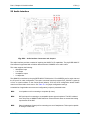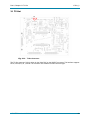
1
phyCORE-AM3517
System on Module and Carrier Board
Hardware Manual
Document No: L-761e_2
Product No: PCM-048/PCM-961
SOM PCB No: 1335.1
CB PCB No: 1336.1
Edition: March 21, 2012
A product of a PHYTEC Technology Holding Company
L-761e_2
phyCORE-AM3517
In this manual are descriptions for copyrighted products that are not explicitly indicated as such. The
absence of the trademark (™) and copyright (©) symbols does not imply that a product is not protected.
Additionally, registered patents and trademarks are similarly not expressly indicated in this manual.
The information in this document has been carefully checked and is believed to be entirely reliable.
However, PHYTEC America LLC assumes no responsibility for any inaccuracies. PHYTEC America LLC
neither gives any guarantee nor accepts any liability whatsoever for consequential damages resulting from
the use of this manual or its associated product. PHYTEC America LLC reserves the right to alter the
information contained herein without prior notification and accepts no responsibility for any damages which
might result.
Additionally, PHYTEC America LLC offers no guarantee nor accepts any liability for damages arising from
the improper usage or improper installation of the hardware or software. PHYTEC America LLC further
reserves the right to alter the layout and/or design of the hardware without prior notification and accepts no
liability for doing so.
© Copyright 2011 PHYTEC America LLC, Bainbridge Island, WA.
Rights - including those of translation, reprint, broadcast, photomechanical or similar reproduction and
storage or processing in computer systems, in whole or in part - are reserved. No reproduction may occur
without the express written consent from PHYTEC America LLC.
EUROPE
NORTH AMERICA
PHYTEC Technologie Holding AG
Robert-Koch-Str. 39
D-55129 Mainz
GERMANY
PHYTEC America LLC
203 Parfitt Way SW, Suite G100
Bainbridge Island, WA 98110
USA
+49 (800) 0749832
1 (800) 278-9913
Technical Support:
+49 (6131) 9221-31
1 (800) 278-9913
Fax:
+49 (6131) 9221-33
1 (206) 780-9135
http://www.phytec.eu/europe
http://www.phytec.com
Address:
Ordering Information:
Website:
© PHYTEC America LLC 2012
L-761e_2
Table of Contents
L-761e_2
Table of Contents
List of Tables. . . . . . . . . . . . . . . . . . . . . . . . . . . . . . . . . . . . . . . . . . . . . . . . . . . . . . . . . .iii
List of Figures . . . . . . . . . . . . . . . . . . . . . . . . . . . . . . . . . . . . . . . . . . . . . . . . . . . . . . . . . v
Conventions, Abbreviations, and Acronyms . . . . . . . . . . . . . . . . . . . . . . . . . . . . . . . . . . . . . . . . . . . . vi
Preface . . . . . . . . . . . . . . . . . . . . . . . . . . . . . . . . . . . . . . . . . . . . . . . . . . . . . . . . . . . . . . . . . . . . . . . . . . .viii
Part I: PCM-048/phyCORE-AM3517 System on Module . . . . . . . . . . . . . . . . . . . . . . . . . . . . . . . . . . . . 1
1 Introduction . . . . . . . . . . . . . . . . . . . . . . . . . . . . . . . . . . . . . . . . . . . . . . . . . . . . . . . . . . . . . . . . . . . . . . . 2
1.1 Block Diagram . . . . . . . . . . . . . . . . . . . . . . . . . . . . . . . . . . . . . . . . . . . . . . . . . . . . . . . . . . . . . 4
1.2 View of the phyCORE-AM3517 . . . . . . . . . . . . . . . . . . . . . . . . . . . . . . . . . . . . . . . . . . . . . . . . 5
2 Pin Description . . . . . . . . . . . . . . . . . . . . . . . . . . . . . . . . . . . . . . . . . . . . . . . . . . . . . . . . . . . . . . . . . . . . 7
3 Jumpers. . . . . . . . . . . . . . . . . . . . . . . . . . . . . . . . . . . . . . . . . . . . . . . . . . . . . . . . . . . . . . . . . . . . . . . . . 19
3.1 Jumper Settings. . . . . . . . . . . . . . . . . . . . . . . . . . . . . . . . . . . . . . . . . . . . . . . . . . . . . . . . . . . 22
4 Power . . . . . . . . . . . . . . . . . . . . . . . . . . . . . . . . . . . . . . . . . . . . . . . . . . . . . . . . . . . . . . . . . . . . . . . . . . 25
4.1 Primary System Power (VIN & VIN_3V3) . . . . . . . . . . . . . . . . . . . . . . . . . . . . . . . . . . . . . . . 25
4.2 Secondary Battery Power (VBAT) . . . . . . . . . . . . . . . . . . . . . . . . . . . . . . . . . . . . . . . . . . . . . 25
4.3 PMIC Supplies (U2) . . . . . . . . . . . . . . . . . . . . . . . . . . . . . . . . . . . . . . . . . . . . . . . . . . . . . . . . 25
4.4 RTC Supplies (U2) . . . . . . . . . . . . . . . . . . . . . . . . . . . . . . . . . . . . . . . . . . . . . . . . . . . . . . . . 26
4.5 Selecting Shunt Resistors for Current Measurements . . . . . . . . . . . . . . . . . . . . . . . . . . . . . 26
4.6 Voltage Supervisor (U2, U21) . . . . . . . . . . . . . . . . . . . . . . . . . . . . . . . . . . . . . . . . . . . . . . . . 26
5 External RTC (U22) . . . . . . . . . . . . . . . . . . . . . . . . . . . . . . . . . . . . . . . . . . . . . . . . . . . . . . . . . . . . . . . . 28
6 System Configuration and Booting . . . . . . . . . . . . . . . . . . . . . . . . . . . . . . . . . . . . . . . . . . . . . . . . . . . . 29
6.1 Boot Process . . . . . . . . . . . . . . . . . . . . . . . . . . . . . . . . . . . . . . . . . . . . . . . . . . . . . . . . . . . . . 32
7 System Memory. . . . . . . . . . . . . . . . . . . . . . . . . . . . . . . . . . . . . . . . . . . . . . . . . . . . . . . . . . . . . . . . . . . 33
7.1 SDRAM (U8, U9) . . . . . . . . . . . . . . . . . . . . . . . . . . . . . . . . . . . . . . . . . . . . . . . . . . . . . . . . . . 33
7.2 NAND Flash (U16). . . . . . . . . . . . . . . . . . . . . . . . . . . . . . . . . . . . . . . . . . . . . . . . . . . . . . . . . 33
7.3 EEPROM (U13) . . . . . . . . . . . . . . . . . . . . . . . . . . . . . . . . . . . . . . . . . . . . . . . . . . . . . . . . . . . 34
7.4 Memory Map . . . . . . . . . . . . . . . . . . . . . . . . . . . . . . . . . . . . . . . . . . . . . . . . . . . . . . . . . . . . . 34
8 Serial Interfaces. . . . . . . . . . . . . . . . . . . . . . . . . . . . . . . . . . . . . . . . . . . . . . . . . . . . . . . . . . . . . . . . . . . 35
8.1 RS-232 Transceiver (U15). . . . . . . . . . . . . . . . . . . . . . . . . . . . . . . . . . . . . . . . . . . . . . . . . . . 35
8.2 Ethernet PHY (U12). . . . . . . . . . . . . . . . . . . . . . . . . . . . . . . . . . . . . . . . . . . . . . . . . . . . . . . . 35
8.3 USB OTG (U1) . . . . . . . . . . . . . . . . . . . . . . . . . . . . . . . . . . . . . . . . . . . . . . . . . . . . . . . . . . . 35
8.4 USB1 Host (U1, U7) . . . . . . . . . . . . . . . . . . . . . . . . . . . . . . . . . . . . . . . . . . . . . . . . . . . . . . . 36
9 Debug Interface (X1) . . . . . . . . . . . . . . . . . . . . . . . . . . . . . . . . . . . . . . . . . . . . . . . . . . . . . . . . . . . . . . . 37
10 Touch Screen Controller (U25) . . . . . . . . . . . . . . . . . . . . . . . . . . . . . . . . . . . . . . . . . . . . . . . . . . . . . . 38
11 General Purpose Memory Controller (U2). . . . . . . . . . . . . . . . . . . . . . . . . . . . . . . . . . . . . . . . . . . . . . 39
12 LCD LVDS Transmitter . . . . . . . . . . . . . . . . . . . . . . . . . . . . . . . . . . . . . . . . . . . . . . . . . . . . . . . . . . . . 40
12.1 LVDS and SOM I/O Voltage (J23) . . . . . . . . . . . . . . . . . . . . . . . . . . . . . . . . . . . . . . . . . . . . 41
13 AM3517 IO and GPMC Bus Voltage . . . . . . . . . . . . . . . . . . . . . . . . . . . . . . . . . . . . . . . . . . . . . . . . . . 42
14 Technical Specifications . . . . . . . . . . . . . . . . . . . . . . . . . . . . . . . . . . . . . . . . . . . . . . . . . . . . . . . . . . . 43
15 Hints for Handling the phyCORE-AM3517 . . . . . . . . . . . . . . . . . . . . . . . . . . . . . . . . . . . . . . . . . . . . . 45
Part II: PCM-961/phyCORE-AM3517 Carrier Board . . . . . . . . . . . . . . . . . . . . . . . . . . . . . . . . . . . . . . .
16 Introduction . . . . . . . . . . . . . . . . . . . . . . . . . . . . . . . . . . . . . . . . . . . . . . . . . . . . . . . . . . . . . . . . . . . . .
17 Overview of Peripherals . . . . . . . . . . . . . . . . . . . . . . . . . . . . . . . . . . . . . . . . . . . . . . . . . . . . . . . . . . .
18 Jumpers. . . . . . . . . . . . . . . . . . . . . . . . . . . . . . . . . . . . . . . . . . . . . . . . . . . . . . . . . . . . . . . . . . . . . . . .
19 phyCORE-AM3517 SOM Connectivity . . . . . . . . . . . . . . . . . . . . . . . . . . . . . . . . . . . . . . . . . . . . . . . .
20 Power . . . . . . . . . . . . . . . . . . . . . . . . . . . . . . . . . . . . . . . . . . . . . . . . . . . . . . . . . . . . . . . . . . . . . . . . .
20.1 Wall Adapter Input (X9) . . . . . . . . . . . . . . . . . . . . . . . . . . . . . . . . . . . . . . . . . . . . . . . . . . . .
20.2 Power over Ethernet (PoE) . . . . . . . . . . . . . . . . . . . . . . . . . . . . . . . . . . . . . . . . . . . . . . . . .
© PHYTEC America LLC 2012
46
47
48
51
55
56
56
57
i
Table of Contents
21
21
22
23
24
25
26
27
28
29
30
31
32
33
34
35
35
36
L-761e_2
20.3 Lithium-Ion Battery . . . . . . . . . . . . . . . . . . . . . . . . . . . . . . . . . . . . . . . . . . . . . . . . . . . . . . .
20.4 3.3V Supply (U27) . . . . . . . . . . . . . . . . . . . . . . . . . . . . . . . . . . . . . . . . . . . . . . . . . . . . . . . .
20.5 1.8V Supply (U31) . . . . . . . . . . . . . . . . . . . . . . . . . . . . . . . . . . . . . . . . . . . . . . . . . . . . . . . .
20.6 Current Measurement . . . . . . . . . . . . . . . . . . . . . . . . . . . . . . . . . . . . . . . . . . . . . . . . . . . . .
...............................................................................
JTAG Connectivity. . . . . . . . . . . . . . . . . . . . . . . . . . . . . . . . . . . . . . . . . . . . . . . . . . . . . . . . . . . . . . . .
Audio Interface . . . . . . . . . . . . . . . . . . . . . . . . . . . . . . . . . . . . . . . . . . . . . . . . . . . . . . . . . . . . . . . . . .
Ethernet Connectivity . . . . . . . . . . . . . . . . . . . . . . . . . . . . . . . . . . . . . . . . . . . . . . . . . . . . . . . . . . . . .
USB Connectivity. . . . . . . . . . . . . . . . . . . . . . . . . . . . . . . . . . . . . . . . . . . . . . . . . . . . . . . . . . . . . . . . .
LCD and DVI Connectivity. . . . . . . . . . . . . . . . . . . . . . . . . . . . . . . . . . . . . . . . . . . . . . . . . . . . . . . . . .
25.1 DVI Connector . . . . . . . . . . . . . . . . . . . . . . . . . . . . . . . . . . . . . . . . . . . . . . . . . . . . . . . . . . .
25.2 LVDS Connectors . . . . . . . . . . . . . . . . . . . . . . . . . . . . . . . . . . . . . . . . . . . . . . . . . . . . . . . .
25.3 TTL LCD Connector . . . . . . . . . . . . . . . . . . . . . . . . . . . . . . . . . . . . . . . . . . . . . . . . . . . . . .
GPIO Expansion Connector . . . . . . . . . . . . . . . . . . . . . . . . . . . . . . . . . . . . . . . . . . . . . . . . . . . . . . . .
RS-232 Connectivity . . . . . . . . . . . . . . . . . . . . . . . . . . . . . . . . . . . . . . . . . . . . . . . . . . . . . . . . . . . . . .
SD/SDIO/MMC Connectivity . . . . . . . . . . . . . . . . . . . . . . . . . . . . . . . . . . . . . . . . . . . . . . . . . . . . . . . .
CAN (Controller Area Network) Interface . . . . . . . . . . . . . . . . . . . . . . . . . . . . . . . . . . . . . . . . . . . . . .
Wireless Connector . . . . . . . . . . . . . . . . . . . . . . . . . . . . . . . . . . . . . . . . . . . . . . . . . . . . . . . . . . . . . . .
TV Out . . . . . . . . . . . . . . . . . . . . . . . . . . . . . . . . . . . . . . . . . . . . . . . . . . . . . . . . . . . . . . . . . . . . . . . . .
Camera Interface. . . . . . . . . . . . . . . . . . . . . . . . . . . . . . . . . . . . . . . . . . . . . . . . . . . . . . . . . . . . . . . . .
User Buttons . . . . . . . . . . . . . . . . . . . . . . . . . . . . . . . . . . . . . . . . . . . . . . . . . . . . . . . . . . . . . . . . . . . .
User LEDs . . . . . . . . . . . . . . . . . . . . . . . . . . . . . . . . . . . . . . . . . . . . . . . . . . . . . . . . . . . . . . . . . . . . . .
...............................................................................
Boot Mode Selection . . . . . . . . . . . . . . . . . . . . . . . . . . . . . . . . . . . . . . . . . . . . . . . . . . . . . . . . . . . . . .
System Reset Button. . . . . . . . . . . . . . . . . . . . . . . . . . . . . . . . . . . . . . . . . . . . . . . . . . . . . . . . . . . . . .
Part III:
58
58
58
59
60
60
62
64
65
67
70
70
71
72
73
77
79
80
82
83
85
87
88
88
92
. . . . . . . . . . . . . . . . . . . . . . . . . . . . . . . . . . . . . . . . . . . . . . . . . . . . . . . . . . . . . . . . . . . . . . . . . . 93
Part III: PCM-988/GPIO Expansion Board . . . . . . . . . . . . . . . . . . . . . . . . . . . . . . . . . . . . . . . . . . . . . . . 93
37 Introduction . . . . . . . . . . . . . . . . . . . . . . . . . . . . . . . . . . . . . . . . . . . . . . . . . . . . . . . . . . . . . . . . . . . . . 94
38 System Signal Mapping. . . . . . . . . . . . . . . . . . . . . . . . . . . . . . . . . . . . . . . . . . . . . . . . . . . . . . . . . . . . 96
39 GPMC Signal Mapping . . . . . . . . . . . . . . . . . . . . . . . . . . . . . . . . . . . . . . . . . . . . . . . . . . . . . . . . . . . . 97
40 UART Signal Mapping . . . . . . . . . . . . . . . . . . . . . . . . . . . . . . . . . . . . . . . . . . . . . . . . . . . . . . . . . . . . . 99
41 I²C Signal Mapping . . . . . . . . . . . . . . . . . . . . . . . . . . . . . . . . . . . . . . . . . . . . . . . . . . . . . . . . . . . . . . 100
42 GPIO Signal Mapping . . . . . . . . . . . . . . . . . . . . . . . . . . . . . . . . . . . . . . . . . . . . . . . . . . . . . . . . . . . . 101
43 USB Signal Mapping . . . . . . . . . . . . . . . . . . . . . . . . . . . . . . . . . . . . . . . . . . . . . . . . . . . . . . . . . . . . . 102
44 CAN Signal Mapping . . . . . . . . . . . . . . . . . . . . . . . . . . . . . . . . . . . . . . . . . . . . . . . . . . . . . . . . . . . . . 103
45 Ethernet Signal Mapping . . . . . . . . . . . . . . . . . . . . . . . . . . . . . . . . . . . . . . . . . . . . . . . . . . . . . . . . . . 104
46 HDQ Signal Mapping. . . . . . . . . . . . . . . . . . . . . . . . . . . . . . . . . . . . . . . . . . . . . . . . . . . . . . . . . . . . . 105
47 McBSP Signal Mapping. . . . . . . . . . . . . . . . . . . . . . . . . . . . . . . . . . . . . . . . . . . . . . . . . . . . . . . . . . . 106
48 SPI Signal Mapping . . . . . . . . . . . . . . . . . . . . . . . . . . . . . . . . . . . . . . . . . . . . . . . . . . . . . . . . . . . . . . 107
49 Power Signal Mapping. . . . . . . . . . . . . . . . . . . . . . . . . . . . . . . . . . . . . . . . . . . . . . . . . . . . . . . . . . . . 108
Revision History . . . . . . . . . . . . . . . . . . . . . . . . . . . . . . . . . . . . . . . . . . . . . . . . . . . . . . . . . . . . . . . . . . 109
© PHYTEC America LLC 2012
ii
List of Tables
L-761e_2
List of Tables
Conventions, Abbreviations, and Acronyms . . . . . . . . . . . . . . . . . . . . . . . . . . . . . . . . . . . . . . . . . . . . . vi
Table i-1. Abbreviations and Acronyms Used in This Manual . . . . . . . . . . . . . . . . . . . . . . . . . . . . vi
Part I: PCM-048/phyCORE-AM3517 System on Module . . . . . . . . . . . . . . . . . . . . . . . . . . . . . . . . . . . . 1
Table 2-1. Pin Descriptions, phyCORE-Connector X2, Row A . . . . . . . . . . . . . . . . . . . . . . . . . . . 8
Table 2-2. Pin Descriptions, phyCORE-Connector X2, Row B . . . . . . . . . . . . . . . . . . . . . . . . . . 10
Table 2-3. Pin Descriptions, phyCORE-Connector X2, Row C . . . . . . . . . . . . . . . . . . . . . . . . . . 13
Table 2-4. Pin Descriptions, phyCORE-Connector X2, Row D . . . . . . . . . . . . . . . . . . . . . . . . . . 15
Table 3-1. Jumper Settings . . . . . . . . . . . . . . . . . . . . . . . . . . . . . . . . . . . . . . . . . . . . . . . . . . . . . 22
Table 4-1. Current Measurements . . . . . . . . . . . . . . . . . . . . . . . . . . . . . . . . . . . . . . . . . . . . . . . . 26
Table 6-1. Peripheral Booting Configuration Pins after POR . . . . . . . . . . . . . . . . . . . . . . . . . . . 29
Table 6-2. Booting Configuration Pins after a Warm Reset . . . . . . . . . . . . . . . . . . . . . . . . . . . . . 30
Table 7-1. Valid SDRAM Memory Address Ranges . . . . . . . . . . . . . . . . . . . . . . . . . . . . . . . . . . 33
Table 7-2. LOCK Pin Jumper Settings . . . . . . . . . . . . . . . . . . . . . . . . . . . . . . . . . . . . . . . . . . . . 34
Table 7-3. phyCORE-AM3517 Memory Map . . . . . . . . . . . . . . . . . . . . . . . . . . . . . . . . . . . . . . . . 34
Table 8-1. UART3 TTL and RS-232 Level Signals . . . . . . . . . . . . . . . . . . . . . . . . . . . . . . . . . . . 35
Table 8-2. Applicable USB Operating Mode Connectors . . . . . . . . . . . . . . . . . . . . . . . . . . . . . . 36
Table 11-1. GPMC Signal Mapping . . . . . . . . . . . . . . . . . . . . . . . . . . . . . . . . . . . . . . . . . . . . . . . 39
Table 14-1. Technical Specifications . . . . . . . . . . . . . . . . . . . . . . . . . . . . . . . . . . . . . . . . . . . . . . 43
Table 14-2. Static Operating Characteristics . . . . . . . . . . . . . . . . . . . . . . . . . . . . . . . . . . . . . . . . 44
Part II: PCM-961/phyCORE-AM3517 Carrier Board . . . . . . . . . . . . . . . . . . . . . . . . . . . . . . . . . . . . . . .
Table 17-1. Connectors and Headers . . . . . . . . . . . . . . . . . . . . . . . . . . . . . . . . . . . . . . . . . . . . .
Table 17-2. Description of the Buttons and Switches . . . . . . . . . . . . . . . . . . . . . . . . . . . . . . . . .
Table 17-3. Description of LEDs . . . . . . . . . . . . . . . . . . . . . . . . . . . . . . . . . . . . . . . . . . . . . . . . .
Table 18-1. Jumper Settings . . . . . . . . . . . . . . . . . . . . . . . . . . . . . . . . . . . . . . . . . . . . . . . . . . . .
Table 20-1. Possible Ethernet PSE Options . . . . . . . . . . . . . . . . . . . . . . . . . . . . . . . . . . . . . . . .
Table 21-1. phyCORE-AM3517 JTAG Connector X13 Pin Descriptions . . . . . . . . . . . . . . . . . .
Table 21-2. Compatible JTAG Probes for the phyCORE-AM3517 Carrier Board . . . . . . . . . . . .
Table 25-1. 24-bit 8:8:8 mode (S1-1,S1-2, S1-3, S1-4 = O,O,O,O) . . . . . . . . . . . . . . . . . . . . . .
Table 25-2. 12-bit 4:4:4 mode (S1-1,S1-2, S1-3, S1-4 = C, C, C, O) . . . . . . . . . . . . . . . . . . . . .
Table 25-3. 16-bit 5:6:5 mode (S1-1,S1-2, S1-3, S1-4 = C, C, O, C) . . . . . . . . . . . . . . . . . . . . .
Table 25-4. 18-bit 6:6:6 mode (S1-1,S1-2, S1-3, S1-4 = C, C, O, O) . . . . . . . . . . . . . . . . . . . . .
Table 25-5. LCD Mode Jumper Summary (S1-1,S1-2, S1-3, S1-4) . . . . . . . . . . . . . . . . . . . . . .
Table 27-1. Connector P1 (UART3) Pin Descriptions . . . . . . . . . . . . . . . . . . . . . . . . . . . . . . . . .
Table 27-2. Connector X29 (UART2) Pin Descriptions . . . . . . . . . . . . . . . . . . . . . . . . . . . . . . . .
Table 27-3. TTL UART Pin Header (X10) Descriptions . . . . . . . . . . . . . . . . . . . . . . . . . . . . . . . .
Table 28-1. SDIO Easy Access Header Connector Signal Descriptions . . . . . . . . . . . . . . . . . . .
Table 30-1. Wireless Connector (X7) Signal Descriptions . . . . . . . . . . . . . . . . . . . . . . . . . . . . .
Table 32-1. Camera Interface (X4) Signal Descriptions . . . . . . . . . . . . . . . . . . . . . . . . . . . . . . .
Table 35-1. Boot Selection Switches and Descriptions . . . . . . . . . . . . . . . . . . . . . . . . . . . . . . . .
Table 35-2. Boot Order Switch Configurations . . . . . . . . . . . . . . . . . . . . . . . . . . . . . . . . . . . . . .
Part III:
46
48
49
49
52
57
60
61
69
69
69
69
70
74
74
75
78
80
83
89
89
. . . . . . . . . . . . . . . . . . . . . . . . . . . . . . . . . . . . . . . . . . . . . . . . . . . . . . . . . . . . . . . . . . . . . . . . . . 93
Part III: PCM-988/GPIO Expansion Board . . . . . . . . . . . . . . . . . . . . . . . . . . . . . . . . . . . . . . . . . . . . . . . 93
Table 37-1. GPIO Expansion Connector - Signals Removed . . . . . . . . . . . . . . . . . . . . . . . . . . . 95
Table 38-1. System Signal Mapping . . . . . . . . . . . . . . . . . . . . . . . . . . . . . . . . . . . . . . . . . . . . . . 96
Table 39-1. GPMC Signal Mapping . . . . . . . . . . . . . . . . . . . . . . . . . . . . . . . . . . . . . . . . . . . . . . . 97
Table 40-1. UART Signal Mapping . . . . . . . . . . . . . . . . . . . . . . . . . . . . . . . . . . . . . . . . . . . . . . . 99
Table 41-1. I²C Signal Mapping . . . . . . . . . . . . . . . . . . . . . . . . . . . . . . . . . . . . . . . . . . . . . . . . . 100
© PHYTEC America LLC 2012
iii
List of Tables
L-761e_2
Table 42-1. GPIO Signal Mapping . . . . . . . . . . . . . . . . . . . . . . . . . . . . . . . . . . . . . . . . . . . . . . .
Table 43-1. USB Signal Mapping . . . . . . . . . . . . . . . . . . . . . . . . . . . . . . . . . . . . . . . . . . . . . . .
Table 44-1. CAN Signal Mapping . . . . . . . . . . . . . . . . . . . . . . . . . . . . . . . . . . . . . . . . . . . . . . .
Table 45-1. Ethernet Signal Mapping . . . . . . . . . . . . . . . . . . . . . . . . . . . . . . . . . . . . . . . . . . . .
Table 46-1. HDQ Signal Mapping . . . . . . . . . . . . . . . . . . . . . . . . . . . . . . . . . . . . . . . . . . . . . . .
Table 47-1. McBSP Signal Mapping . . . . . . . . . . . . . . . . . . . . . . . . . . . . . . . . . . . . . . . . . . . . .
Table 48-1. SPI Signal Mapping . . . . . . . . . . . . . . . . . . . . . . . . . . . . . . . . . . . . . . . . . . . . . . . .
Table 49-1. Power Signal Mapping . . . . . . . . . . . . . . . . . . . . . . . . . . . . . . . . . . . . . . . . . . . . . .
101
102
103
104
105
106
107
108
Revision History . . . . . . . . . . . . . . . . . . . . . . . . . . . . . . . . . . . . . . . . . . . . . . . . . . . . . . . . . . . . . . . . . . 109
Table 50-1. Revision History . . . . . . . . . . . . . . . . . . . . . . . . . . . . . . . . . . . . . . . . . . . . . . . . . . . 109
© PHYTEC America LLC 2012
iv
List of Figures
L-761e_2
List of Figures
Part I: PCM-048/phyCORE-AM3517 System on Module. . . . . . . . . . . . . . . . . . . . . . . . . . . . . . . . . . . . . 1
Fig. 1-1. phyCORE-AM3517 Block Diagram . . . . . . . . . . . . . . . . . . . . . . . . . . . . . . . . . . . . . . . . . 4
Fig. 1-2. Top View of the phyCORE-AM3517 (Controller Side) . . . . . . . . . . . . . . . . . . . . . . . . . . . 5
Fig. 1-3. Bottom View of the phyCORE-AM3517 (Connector Side) . . . . . . . . . . . . . . . . . . . . . . . . 6
Fig. 2-1. Pin-out of the phyCORE-Connector
(Top View, with Cross Section Insert) . . . . . . . . . . . . . . . . . . . . . . . . . . . . . . . . . . . . . . . . . . . . . . 8
Fig. 3-1. Jumper Locations (Connector Side). . . . . . . . . . . . . . . . . . . . . . . . . . . . . . . . . . . . . . . . 19
Fig. 3-2. Jumper Locations (Controller Side) . . . . . . . . . . . . . . . . . . . . . . . . . . . . . . . . . . . . . . . . 20
Fig. 3-3. Default Jumper Settings (Connector Side). . . . . . . . . . . . . . . . . . . . . . . . . . . . . . . . . . . 21
Fig. 3-4. Default Jumper Settings (Controller Side) . . . . . . . . . . . . . . . . . . . . . . . . . . . . . . . . . . . 22
Fig. 9-1. JTAG Interface X1 (Controller Side). . . . . . . . . . . . . . . . . . . . . . . . . . . . . . . . . . . . . . . . 37
Fig. 12-1. LVDS Multiplexing Scheme1 . . . . . . . . . . . . . . . . . . . . . . . . . . . . . . . . . . . . . . . . . . . . 40
Fig. 14-1. phyCORE-AM3517 Physical Dimensions . . . . . . . . . . . . . . . . . . . . . . . . . . . . . . . . . . 43
Part II: PCM-961/phyCORE-AM3517 Carrier Board . . . . . . . . . . . . . . . . . . . . . . . . . . . . . . . . . . . . . . .
Fig. 16-1. phyCORE-AM3517 Carrier Board . . . . . . . . . . . . . . . . . . . . . . . . . . . . . . . . . . . . . . . .
Fig. 17-1. Overview of Peripherals . . . . . . . . . . . . . . . . . . . . . . . . . . . . . . . . . . . . . . . . . . . . . . . .
Fig. 18-1. Jumper Locations and Default Settings . . . . . . . . . . . . . . . . . . . . . . . . . . . . . . . . . . . .
Fig. 18-2. Typical Jumper Pad Numbering Scheme (Removable Jumpers) . . . . . . . . . . . . . . . .
Fig. 19-1. phyCORE-AM3517 SOM Connectivity to the Carrier Board . . . . . . . . . . . . . . . . . . . .
Fig. 20-1. Powering Scheme . . . . . . . . . . . . . . . . . . . . . . . . . . . . . . . . . . . . . . . . . . . . . . . . . . . .
Fig. 21-1. JTAG Probe Connectivity to the phyCORE-AM3517 . . . . . . . . . . . . . . . . . . . . . . . . . .
Fig. 22-1. Audio Interface Connectors and Jumpers . . . . . . . . . . . . . . . . . . . . . . . . . . . . . . . . . .
Fig. 23-1. Ethernet Interface Connector and LEDs . . . . . . . . . . . . . . . . . . . . . . . . . . . . . . . . . . .
Fig. 24-1. USB Interface Connectors and Jumpers . . . . . . . . . . . . . . . . . . . . . . . . . . . . . . . . . . .
Fig. 25-1. LCD/DVI Interface Connectors, Jumpers, and Switches . . . . . . . . . . . . . . . . . . . . . . .
Fig. 25-2. LCD Signal Mapping in 24-bit Mode with a 24-bit LCD . . . . . . . . . . . . . . . . . . . . . . . .
Fig. 25-3. LCD Signal Mapping in 16-bit Mode with an 16-Bit LCD . . . . . . . . . . . . . . . . . . . . . . .
Fig. 26-1. GPIO Expansion Connector . . . . . . . . . . . . . . . . . . . . . . . . . . . . . . . . . . . . . . . . . . . . .
Fig. 27-1. RS-232 Interface Connectors and Jumpers . . . . . . . . . . . . . . . . . . . . . . . . . . . . . . . . .
Fig. 27-2. DB9 RS-232 Connectors P1 (UART3) Pin Numbering . . . . . . . . . . . . . . . . . . . . . . . .
Fig. 27-3. Connector X29 (UART2) Pin Numbering . . . . . . . . . . . . . . . . . . . . . . . . . . . . . . . . . . .
Fig. 27-4. UART3/UART2 Header Connector X10 Pin Numbering . . . . . . . . . . . . . . . . . . . . . . .
Fig. 28-1. SDIO Interface Connectors and Jumpers . . . . . . . . . . . . . . . . . . . . . . . . . . . . . . . . . .
Fig. 29-1. CAN Interface Connectors and Jumpers . . . . . . . . . . . . . . . . . . . . . . . . . . . . . . . . . . .
Fig. 30-1. Wireless Interface Connector . . . . . . . . . . . . . . . . . . . . . . . . . . . . . . . . . . . . . . . . . . . .
Fig. 31-1. TV Out Connector . . . . . . . . . . . . . . . . . . . . . . . . . . . . . . . . . . . . . . . . . . . . . . . . . . . .
Fig. 32-1. Camera Interface Connectors and Jumpers . . . . . . . . . . . . . . . . . . . . . . . . . . . . . . . .
Fig. 33-1. User Buttons and Jumpers . . . . . . . . . . . . . . . . . . . . . . . . . . . . . . . . . . . . . . . . . . . . . .
Fig. 34-1. User LEDs and Jumpers . . . . . . . . . . . . . . . . . . . . . . . . . . . . . . . . . . . . . . . . . . . . . . .
Fig. 35-1. Boot Mode Selection Connectors and Jumpers . . . . . . . . . . . . . . . . . . . . . . . . . . . . . .
Fig. 35-2. Boot Switches - Default Settings . . . . . . . . . . . . . . . . . . . . . . . . . . . . . . . . . . . . . . . . .
Fig. 36-1. System Reset Button . . . . . . . . . . . . . . . . . . . . . . . . . . . . . . . . . . . . . . . . . . . . . . . . . .
46
47
48
51
51
55
56
60
62
64
65
67
68
68
72
73
73
74
75
77
79
80
82
83
85
87
88
88
92
Part III: . . . . . . . . . . . . . . . . . . . . . . . . . . . . . . . . . . . . . . . . . . . . . . . . . . . . . . . . . . . . . . . . . . . . . . . . . . . 93
Part III: PCM-988/GPIO Expansion Board . . . . . . . . . . . . . . . . . . . . . . . . . . . . . . . . . . . . . . . . . . . . . . . 93
Fig. 37-1. PCM-988/GPIO Expansion Board and Patch Field . . . . . . . . . . . . . . . . . . . . . . . . . . . 94
© PHYTEC America LLC 2012
v
L-761e_2
Conventions, Abbreviations, and Acronyms
Conventions
The conventions used in this manual are as follows:
• Signals that are preceded by a “/” character are designated as active low signals. Their active
state is when they are driven low, or are driving low; for example: /RESET.
• Tables show the default setting or jumper position in bold, teal text.
• Text in blue indicates a hyperlink, either internal or external to the document. Click these links to
quickly jump to the applicable URL, part, chapter, table, or figure.
• References made to the phyCORE-Connector always refer to the high density molex connectors
on the underside of the phyCORE-AM3517 System on Module.
Abbreviations and Acronyms
Many acronyms and abbreviations are used throughout this manual. Use the table below to navigate
unfamiliar terms used in this document.
Table i-1. Abbreviations and Acronyms Used in This Manual
Abbreviation
Definition
BTN1
User button 1; used in reference to one of the four available user buttons on the Carrier Board
BTN2
User button 2; used in reference to one of the four available user buttons on the Carrier Board
BTN3
User button 3; used in reference to one of the four available user buttons on the Carrier Board
BTN4
User button 4; used in reference to one of the four available user buttons on the Carrier Board
CB
Carrier Board; used in reference to the PCM-961/phyCORE-AM3517 Carrier Board
CPLD
Complex Programmable Logic Device
EMI
Electromagnetic Interference
GPI
General purpose input
GPIO
General purpose input and output
GPIOEBPF
GPIO Expansion Board Patch Field; used in reference with the PCM-988/GPIO
Expansion Board and its associated patch field
GPMC
General Purpose Memory Controller
GPO
General purpose output
J
Solder jumper; these types of jumpers require solder equipment to remove and
place
JP
Solderless jumper; these types of jumpers can be removed and placed by hand with
no special tools
PCB
Printed circuit board
PoE
Power over Ethernet
POT
Potentiometer
PMIC
Power Management Integrated Circuit
PSE
Power sourcing equipment; the device in a PoE network that provides power to connected devices - usually a switch, router, or stand alone power injector
© PHYTEC America LLC 2012
vi
L-761e_2
Table i-1. Abbreviations and Acronyms Used in This Manual
Abbreviation
Definition
RTC
Real-time clock
SMT
Surface mount technology
SOM
System on Module; used in reference to the PCM-048/phyCORE-AM3517 System
on Module
TRM
Technical Reference Manual
VBAT
SOM battery supply input
VFP
Vector Floating Point
© PHYTEC America LLC 2012
vii
L-761e_2
Preface
This phyCORE-AM3517 Hardware Manual describes the System on Module's design and functions.
Precise specifications for the Texas Instruments AM3517 processor can be found in the processor
datasheet and/or user's manual.
In this hardware manual and in the schematics, active low signals are denoted by a "/" preceding the signal
name, for example: /RD. A "0" represents a logic-zero or low-level signal, while a "1" represents a logicone or high-level signal.
Declaration of Electro Magnetic Conformity of the PHYTEC
phyCORE-AM3517
PHYTEC System on Modules (SOMs) are designed for installation in electrical appliances or, combined
with the PHYTEC Carrier Board, can be used as dedicated Evaluation Boards (for use as a test and
prototype platform for hardware/software development) in laboratory environments.
CAUTION:
PHYTEC products lacking protective enclosures are subject to damage by ESD and, hence, may only be
unpacked, handled or operated in environments in which sufficient precautionary measures have been
taken in respect to ESD-dangers. It is also necessary that only appropriately trained personnel (such as
electricians, technicians and engineers) handle and/or operate these products. Moreover, PHYTEC
products should not be operated without protection circuitry if connections to the product's pin header
rows are longer than 3 m.
PHYTEC products fulfill the norms of the European Union's Directive for Electro Magnetic Conformity only
in accordance to the descriptions and rules of usage indicated in this hardware manual (particularly in
respect to the pin header row connectors, power connector and serial interface to a host-PC).
Implementation of PHYTEC products into target devices, as well as user modifications and extensions of
PHYTEC products, is subject to renewed establishment of conformity to, and certification of, Electro
Magnetic Directives. Users should ensure conformance following any modifications to the products as
well as implementation of the products into target systems.
The phyCORE-AM3517 is one of a series of PHYTEC System on Modules that can be populated with
different controllers and, hence, offers various functions and configurations. PHYTEC supports a variety of
8-/16- and 32-bit controllers in two ways:
1. As the basis for Rapid Development Kits which serve as a reference and evaluation platform.
2. As insert-ready, fully functional phyCORE OEM modules, which can be embedded directly into the
user's peripheral hardware design.
Implementation of an OEM-able SOM subassembly as the "core" of your embedded design allows you to
focus on hardware peripherals and firmware without expending resources to "re-invent" microcontroller
circuitry. Furthermore, much of the value of the phyCORE module lies in its layout and test.
Production-ready Board Support Packages (BSPs) and Design Services for our hardware further reduce
development time and expenses. Take advantage of PHYTEC products to shorten time-to-market, reduce
development costs, and avoid substantial design issues and risks. For more information go to:
http://www.phytec.com/services/design-services/index.html
© PHYTEC America LLC 2012
viii
PCM-048/phyCORE-AM3517 System on Module
L-761e_2
Part I: PCM-048/phyCORE-AM3517 System on
Module
Part 1 of this three part manual provides detailed information on the phyCORE-AM3517 System on Module
(SOM) designed for custom integration into customer applications.
The information in the following chapters is applicable to the 1335.1 PCB revision of the phyCOREAM3517 SOM.
© PHYTEC America LLC 2012
1
Part I, Chapter 1: Introduction
L-761e_2
1 Introduction
The phyCORE-AM3517 belongs to PHYTEC’s phyCORE System on Module (SOM) family. The
phyCORE SOMs represent the continuous development of PHYTEC SOM technology. Like its mini-,
micro-, and nanoMODUL predecessors, the phyCORE boards integrate all core elements of a
microcontroller system on a subminiature board and are designed in a manner that ensures their easy
expansion and embedding in peripheral hardware developments.
As independent research indicates that approximately 70% of all EMI (Electro Magnetic Interference)
problems stem from insufficient supply voltage grounding of electronic components in high frequency
environments, the phyCORE board design features an increased pin package. The increased pin package
allows dedication of approximately 20% of all connector pins on the phyCORE boards to ground. This
improves EMI and EMC characteristics and makes it easier to design complex applications meeting EMI
and EMC guidelines using phyCORE boards even in high noise environments.
phyCORE boards achieve their small size through modern SMD technology and multi-layer design. In
accordance with the complexity of the module, 0402-packaged SMD components and laser-drilled
Microvias are used on the boards, providing phyCORE users with access to this cutting edge
miniaturization technology for integration into their own design.
The phyCORE-AM3517 is a sub-miniature (72 x 58 mm) insert-ready SOM populated with Texas
Instruments AM3517 ARM Cortex-A8 core processor. Its universal design enables its insertion into a wide
range of embedded applications. All processor signals and ports extend from the processor to high-density
pitch (0.635 mm) connectors aligning two sides of the board. This allows the SOM to be plugged like a "big
chip" into a target application.
Precise specifications for the processor populating the board can be found in the applicable processor
user's manual and datasheet. The descriptions in this manual are based on the Texas Instruments ARM
Cortex A8/AM3517 processor. No description of compatible processor derivative functions is included, as
such functions are not relevant for the basic functioning of the phyCORE-AM3517.
The phyCORE-AM3517 offers the following features:
• Insert-ready, sub-miniature (72 x 58 mm) System on Module (SOM) subassembly in low EMI
design, achieved through advanced SMD technology
• Populated with the Texas Instruments AM3517 processor (491-ball BGA packaging)
• Improved interference safety achieved through multi-layer PCB technology and dedicated ground
pins
• Controller signals and ports extend to two 160-pin high-density (0.635 mm) Molex connectors
aligning two sides of the board, enabling it to be plugged like a "big chip" into target application
• Maximum 600 MHz core clock frequency
• NEON (TM) SIMD co-processor and Vector Floating Point (VFP) co-processor
• 16KB instruction cache (4-way set-associative)
• 16KB data cache (4-way set-associative)
• 256KB L2 cache
• System direct memory access (sDMA) controller (32 logical channels with configurable priority)
• Memory Management Unit (MMU)
• 32-bit DDR2-333MHz, 256 or 512MByte SDRAM running at 1.8V
• General Purpose Memory Controller supporting 16-bit wide multiplexed address/data bus
• 12 32-bit General Purpose Timers
• 64 KB SRAM
• 128, 256, or 512 MB of on-board NAND flash at 1.8V (bootable)
• HD resolution display subsystem:
- Parallel Digital Output
- Up to 24-Bit RGB
© PHYTEC America LLC 2012
2
Part I, Chapter 1: Introduction
L-761e_2
-
•
•
•
•
•
•
•
•
•
•
•
•
•
•
•
•
•
•
•
•
•
•
•
Supports up to two LCD Panels
Support for Remote Frame Buffer Interface (RFBI) LCD Panels supporting
Two 10-bit Digital-to-Analog Converters (DACs) supporting Composite NTSC/PAL Video and
Luma/Chroma Separate Video (S-Video)
- Rotation 90, 180, and 270 degrees; image resizing from 1/4x to 8x
- Color Space Converter
- 8-bit Alpha Blending
Video Processing Front End (VPFE) 16-bit video input port:
- RAW data interface
- 75-MHz maximum pixel clock
- Supports REC656/CCIR656 standard chip
- Supports YCbCr422 format (8-bit or 16-bit with discrete horizontal and vertical sync signals)
- Generates optical black clamping signals
- Built-in digital clamping and black level compensation
- 10-bit to 8-bit A-law compression hardware
- Up to 16K Pixels (Image Size) in horizontal and vertical directions
10/100 Mbit Ethernet (MAC and PHY)
Multiport USB Host Subsystem [HS/FS/LS] DP/DM interface
USB OTG transceiver for embedded USB host/peripheral functionality
High-End CAN Controller (HECC)
Six rail voltage supervision PMIC with programmable processor core voltage support and RTC
priority voltage switch
One 32-bit Watchdog Timer (internal to AM3517)
Support for RealView ICE debug through standard JTAG interface
Four Master/Slave Multichannel Serial Port Interface (McSPI) ports
Five Multichannel Buffered Serial Ports: one 5K-Byte Transmit/Receive Buffer (McBSP2) and four
512-Byte transmit/receive buffers (McBSP1/3/4/5)
Three Master/Slave high-speed Inter-Integrated circuit (I²C) controllers
Two I²C ports
10/100 Ethernet with HP Auto MDIX support
24-bit LCD controller supporting STN and TFT panels at up to 1024x768 display resolution at
60Hz and 2048x2048 resolution at lower frame rates (PCLK max 75MHz).
Touch screen controller
Three removable media interfaces [MMC/SD/SDIO]
Real-time clock (RTC) with dedicated interrupt (alarm clock function) and processor independent
RTC consuming less than 275nA at 3.0V typical
Boot from NAND, USB, MMC/SDIO, Ethernet, and more
JTAG interface for debugging and download of user code
Up to 186 General-Purpose I/O (GPIO) pins
Configurable IO voltage of 1.8V or 3.3V
Single input supply voltage of 3.3 to 5.0V
Industrial temperature range (-40C to +85C)
© PHYTEC America LLC 2012
3
Part I, Chapter 1: Introduction
L-761e_2
1.1 Block Diagram
Fig. 1-1. phyCORE-AM3517 Block Diagram
© PHYTEC America LLC 2012
4
Part I, Chapter 1: Introduction
L-761e_2
1.2 View of the phyCORE-AM3517
Fig. 1-2. Top View of the phyCORE-AM3517 (Controller Side)
© PHYTEC America LLC 2012
5
Part I, Chapter 1: Introduction
L-761e_2
Fig. 1-3. Bottom View of the phyCORE-AM3517 (Connector Side)
© PHYTEC America LLC 2012
6
Part I, Chapter 2: Pin Description
L-761e_2
2 Pin Description
Please note that all module connections are not to exceed their expressed maximum voltage or current.
Maximum signal input values are indicated in the corresponding controller manuals/datasheets. As
damage from improper connections varies according to use and application, it is the user's responsibility to
take appropriate safety measures to ensure that the module connections are protected from overloading
through connected peripherals.
All controller signals extend to surface mount technology (SMT) connectors (0.635 mm) lining two sides of
the module (referred to as the phyCORE-Connector). This allows the phyCORE-AM3517 to be plugged
into any target application like a "big chip."
The numbering scheme for the phyCORE-Connector is based on a two dimensional matrix in which
column positions are identified by a letter and row position by a number. Pin 1A, for example, is always
located in the upper left hand corner of the matrix. The pin numbering values increase moving down on the
board. Lettering of the pin connector rows progresses alphabetically from left to right (refer to Figure 2-1).
The numbered matrix can be aligned with the phyCORE-AM3517 (viewed from above; phyCOREConnector pointing down) or with the socket of the corresponding phyCORE Carrier Board/user target
circuitry. The upper left-hand corner of the numbered matrix (pin 1A) is thus covered with the corner of the
phyCORE-AM3517 marked with a number 1. The numbering scheme is always in relation to the PCB as
viewed from above, even if all connector contacts extend to the bottom of the module.
The numbering scheme is thus consistent for both the module’s phyCORE-Connector as well as mating
connectors on the phyCORE Carrier Board or target hardware, thereby considerably reducing the risk of
pin identification errors.
Since the pins are exactly defined according to the numbered matrix previously described, the phyCOREConnector is usually assigned a single designator for its position (X2 for example). In this manner the
phyCORE-Connector comprises a single, logical unit regardless of the fact that it could consist of more
than one physical socketed connector. The location of row 1 on the board is marked by a number 1 on the
PCB to allow easy identification.
Figure 2-1 illustrates the numbered matrix system. It shows a phyCORE-AM3517 with SMT phyCOREConnectors on its underside (defined as dotted lines) mounted on a Carrier Board. In order to facilitate
understanding of the pin assignment scheme, the diagram presents a cross-view of the phyCORE module
showing these phyCORE-Connectors mounted on the underside of the module’s PCB.
© PHYTEC America LLC 2012
7
Part I, Chapter 2: Pin Description
L-761e_2
Fig. 2-1. Pin-out of the phyCORE-Connector
(Top View, with Cross Section Insert)
Table 2-1. Pin Descriptions, phyCORE-Connector X2, Row A
I/O
Signal
Level
GPMC_NCS7
O
VDDSHV
2A
GND
-
-
3A
GPMC_NCS3
O
VDDSHV
GPMC interface - control (active low chip select 3)
4A
GPMC_NCS2
O
VDDSHV
GPMC interface - control (active low chip select 2)
5A
GPMC_NCS1
O
VDDSHV
GPMC interface - control (active low chip select 1)
6A
xGPMC_NWE
O
VDDSHV
GPMC interface - control (active low write enable)
7A
GND
-
-
8A
GPMC_NBE0_CLE
O
VDDSHV
GPMC interface - control (active low bus enable 0)
9A
GPMC_NBE1
O
VDDSHV
GPMC interface - control (active low bus enable 1)
10A
GPMC_WAIT0
I
VDDSHV
GPMC interface - control (active low wait signal)
11A
GPMC_WAIT2
I
VDDSHV
GPMC interface - control (active low wait signal)
12A
GND
-
-
13A
GPMC_A9
O
VDDSHV
GPMC interface - address
14A
GPMC_A8
O
VDDSHV
GPMC interface - address
15A
GPMC_A7
O
VDDSHV
GPMC interface - address
16A
GPMC_A4
O
VDDSHV
GPMC interface - address
17A
GND
-
-
18A
GPMC_A1
O
VDDSHV
GPMC interface - address
19A
GPMC_D15
I
VDDSHV
GPMC interface - data
20A
GPMC_D14
I
VDDSHV
GPMC interface - data
21A
GPMC_D11
I
VDDSHV
GPMC interface - data
22A
GND
-
-
Pin
Signal
1A
© PHYTEC America LLC 2012
Description
GPMC interface - control (active low chip select 7)
Ground
Ground
Ground
Ground
Ground
8
Part I, Chapter 2: Pin Description
L-761e_2
Table 2-1. Pin Descriptions, phyCORE-Connector X2, Row A (Continued)
I/O
Signal
Level
GPMC_D8
I
VDDSHV
GPMC interface - data
24A
GPMC_D7
I
VDDSHV
GPMC interface - data
25A
GPMC_D6
I
VDDSHV
GPMC interface - data
26A
GPMC_D3
I
VDDSHV
GPMC interface - data
27A
GND
-
-
28A
GPMC_D0
I
VDDSHV
GPMC interface - data
29A
CCDC_WEN
I
VDDSHV
CCD Camera interface - control (write enable)
30A
CCDC_VD
IO
VDDSHV
CCD Camera interface - control (vertical sync)
31A
CCDC_FIELD
IO
VDDSHV
CCD Camera interface - control (field identification)
32A
GND
-
-
33A
CCDC_DATA5
I
VDDSHV
CCD Camera interface - data
34A
CCDC_DATA4
I
VDDSHV
CCD Camera interface - data
35A
CCDC_DATA3
I
VDDSHV
CCD Camera interface - data
36A
CCDC_DATA0
I
VDDSHV
CCD Camera interface - data
37A
GND
-
-
38A
RMII_MDIO_CLK
O
VDDSHV
Ethernet - MDIO interface clock
39A
RMII_MDIO_DATA
IO
VDDSHV
Ethernet - MDIO interface data
40A
RMII_RXD1
I
VDDSHV
Ethernet MAC - RMII data RX data
41A
RMII_RXER
I
VDDSHV
Ethernet MAC - RMII data RX error
42A
GND
-
-
43A
ETK_D15
O
VDDSHV
ARM Embedded Toolkit debug interface (other signal on HSUSB interface)
44A
ETK_D14
O
VDDSHV
ARM Embedded Toolkit debug interface (other signal on HSUSB interface)
45A
ETK_D13
O
VDDSHV
ARM Embedded Toolkit debug interface (other signal on HSUSB interface)
46A
ETK_D10
O
VDDSHV
ARM Embedded Toolkit debug interface (other signal on HSUSB interface)
47A
GND
-
-
48A
HSUSB1_DATA3
IO
VDDSHV
High Speed USB digital interface - data
49A
HSUSB1_DATA6
IO
VDDSHV
High Speed USB digital interface - data
50A
HSUSB1_DATA5
IO
VDDSHV
High Speed USB digital interface - data
51A
HSUSB1_DATA2
IO
VDDSHV
High Speed USB digital interface - data
52A
GND
-
-
53A
HSUSB1_STP
O
VDDSHV
High Speed USB digital interface - control
54A
xHSUSB1_CLK
O
VDDSHV
High speed USB digital interface 1 - clock
55A
MMC2_DAT7
IO
VDDSHV
MMC / SDIO 2 interface - data
56A
MMC2_DAT4
IO
VDDSHV
MMC / SDIO 2 interface - data
Pin
Signal
23A
© PHYTEC America LLC 2012
Description
Ground
Ground
Ground
Ground
Ground
Ground
9
Part I, Chapter 2: Pin Description
L-761e_2
Table 2-1. Pin Descriptions, phyCORE-Connector X2, Row A (Continued)
I/O
Signal
Level
-
-
MMC2_DAT1
IO
VDDSHV
MMC / SDIO 2 interface - data
59A
MMC2_DAT0
IO
VDDSHV
MMC / SDIO 2 interface - data
60A
MMC2_CMD
O
VDDSHV
MMC / SDIO 2 interface - command
61A
MCSPI2_CS1
O
VDDSHV
Multichannel Serial Peripheral Interface 2 - chip
select 1
62A
GND
-
-
63A
MCSPI2_CS0
IO
VDDSHV
Multichannel Serial Peripheral Interface 2 - chip
select 0
64A
MCSPI2_SIMO
IO
VDDSHV
Multichannel Serial Peripheral Interface 2 - slave
data in, master data out
65A
MCSPI2_SOMI
IO
VDDSHV
Multichannel Serial Peripheral Interface 2 - slave
data out, master data in
66A
xMCSPI2_CLK
IO
VDDSHV
Multichannel Buffered Serial Port 2 - clock
67A
GND
-
-
68A
TV_OUT1
O
Analog
TV Out signal 1
69A
TV_OUT2
O
Analog
TV Out signal 2
70A
MCBSP4_CLKX
IO
VDDSHV
Multichannel Buffered Serial Port 4 - TX clock
71A
MCBSP4_DR
I
VDDSHV
Multichannel Buffered Serial Port 4 - data receive
72A
GND
-
-
73A
MCBSP4_DX
IO
VDDSHV
Multichannel Buffered Serial Port 4 - data transmit
74A
MCBSP4_FSX
IO
VDDSHV
Multichannel Buffered Serial Port 4 - frame sync
transmit
75A
N/C
-
-
76A
JTAG_EMU0
IO
VDDSHV
77A
GND
-
-
78A
JTAG_NTRST
I
VDDSHV
JTAG - test reset
79A
JTAG_TDI
I
VDDSHV
JTAG - test data in
80A
xJTAG_TDO
O
VDDSHV
JTAG - test data out
Pin
Signal
57A
GND
58A
Description
Ground
Ground
Ground
Ground
No connect
JTAG - test emulation
Ground
Table 2-2. Pin Descriptions, phyCORE-Connector X2, Row B
I/O
Signal
Level
GPMC_NCS6
O
VDDSHV
GPMC interface - control
2B
GPMC_NCS5
O
VDDSHV
GPMC interface - control
3B
GPMC_NCS4
O
VDDSHV
GPMC interface - control
4B
GND
-
-
Ground
5B
N/C
-
-
No connect
Pin
Signal
1B
© PHYTEC America LLC 2012
Description
10
Part I, Chapter 2: Pin Description
L-761e_2
Table 2-2. Pin Descriptions, phyCORE-Connector X2, Row B (Continued)
I/O
Signal
Level
GPMC_NWP
O
VDDSHV
GPMC interface - control (active low write protect)
7B
GPMC_NOE
O
VDDSHV
GPMC interface - control (active low output enable)
8B
xGPMC_NADV_ALE
O
VDDSHV
GPMC interface - control
9B
GND
-
-
10B
GPMC_WAIT1
I
VDDSHV
GPMC interface - control (active low wait)
11B
GPMC_WAIT3
I
VDDSHV
GPMC interface - control (active low wait)
12B
xGPMC_CLK
O
VDDSHV
GPMC interface - clock
13B
GPMC_A10
O
VDDSHV
GPMC interface - address
14B
GND
-
-
15B
GPMC_A6
O
VDDSHV
GPMC interface - address
16B
GPMC_A5
O
VDDSHV
GPMC interface - address
17B
GPMC_A3
O
VDDSHV
GPMC interface - address
18B
GPMC_A2
O
VDDSHV
GPMC interface - address
19B
GND
-
-
20B
GPMC_D13
I
VDDSHV
GPMC interface - data
21B
GPMC_D12
I
VDDSHV
GPMC interface - data
22B
GPMC_D10
I
VDDSHV
GPMC interface - data
23B
GPMC_D9
I
VDDSHV
GPMC interface - data
24B
GND
-
-
25B
GPMC_D5
I
VDDSHV
GPMC interface - data
26B
GPMC_D4
I
VDDSHV
GPMC interface - data
27B
GPMC_D2
I
VDDSHV
GPMC interface - data
28B
GPMC_D1
I
VDDSHV
GPMC interface - data
29B
GND
-
-
30B
CCDC_PCLK
IO
VDDSHV
CCD Camera interface - control (pixel clock)
31B
CCDC_HD
IO
VDDSHV
CCD Camera interface - control (horizontal sync)
32B
CCDC_DATA7
I
VDDSHV
CCD Camera interface - data
33B
CCDC_DATA6
I
VDDSHV
CCD Camera interface - data
34B
GND
-
-
35B
CCDC_DATA2
I
VDDSHV
CCD Camera interface - data
36B
CCDC_DATA1
I
VDDSHV
CCD Camera interface - data
37B
RMII_50MHZ_CLK
I
VDDSHV
Ethernet MAC - RMII clock
38B
RMII_CRS_DV
I
VDDSHV
Ethernet MAC - RMII data valid
39B
GND
-
-
40B
RMII_RXD0
I
VDDSHV
Ethernet MAC - RMII data RX data
41B
RMII_TXD1
O
VDDSHV
Ethernet MAC - RMII data TX data
42B
RMII_TXD0
O
VDDSHV
Ethernet MAC - RMII data TX data
43B
RMII_TXEN
O
VDDSHV
Ethernet MAC - RMII data TX enable
Pin
Signal
6B
© PHYTEC America LLC 2012
Description
Ground
Ground
Ground
Ground
Ground
Ground
Ground
11
Part I, Chapter 2: Pin Description
L-761e_2
Table 2-2. Pin Descriptions, phyCORE-Connector X2, Row B (Continued)
I/O
Signal
Level
GND
-
-
45B
ETK_D12
O
VDDSHV
ARM Embedded Toolkit debug interface (other signal
on HSUSB interface)
46B
ETK_D11
O
VDDSHV
ARM Embedded Toolkit debug interface (other signal
on HSUSB interface)
47B
HSUSB1_NXT
I
VDDSHV
High Speed USB digital interface - control
48B
HSUSB1_DIR
I
VDDSHV
High Speed USB digital interface - control
49B
GND
-
-
50B
HSUSB1_DATA4
IO
VDDSHV
High Speed USB digital interface - data
51B
HSUSB1_DATA7
IO
VDDSHV
High Speed USB digital interface - data
52B
HSUSB1_DATA1
IO
VDDSHV
High Speed USB digital interface - data
53B
HSUSB1_DATA0
IO
VDDSHV
High Speed USB digital interface - data
54B
GND
-
-
55B
MMC2_DAT6
IO
VDDSHV
MMC / SDIO 2 interface - data
56B
MMC2_DAT5
IO
VDDSHV
MMC / SDIO 2 interface - data
57B
MMC2_DAT3
IO
VDDSHV
MMC / SDIO 2 interface - data
58B
MMC2_DAT2
IO
VDDSHV
MMC / SDIO 2 interface - data
59B
GND
-
-
60B
xMMC2_CLK
O
VDDSHV
MMC / SDIO 2 interface - clock
61B
I2C3_SCL
O
VDDSHV
I²C bus 3 clock
62B
I2C3_SDA
IO
VDDSHV
I²C bus 3 data
63B
UART1_RTS
O
VDDSHV
UART 1 ready to send
64B
GND
-
-
65B
UART1_CTS
I
VDDSHV
66B
N/C
-
-
No connect
67B
N/C
-
-
No connect
68B
N/C
-
-
No connect
69B
GND
-
-
Ground
70B
MCBSP3_CLKX
IO
VDDSHV
Multichannel Buffered Serial Port 3 - TX clock
71B
MCBSP3_DR
I
VDDSHV
Multichannel Buffered Serial Port 3 - data receive
72B
MCBSP3_DX
IO
VDDSHV
Multichannel Buffered Serial Port 3 - data transmit
73B
MCBSP3_FSX
IO
VDDSHV
Multichannel Buffered Serial Port 3 - frame sync transmit
74B
GND
-
-
Ground
75B
N/C
-
-
No connect
76B
JTAG_EMU1
IO
VDDSHV
JTAG - test emulation
77B
xJTAG_RTCK
O
VDDSHV
JTAG - test clock - ARM clock emulation
Pin
Signal
44B
© PHYTEC America LLC 2012
Description
Ground
Ground
Ground
Ground
Ground
UART 1 clear to send
12
Part I, Chapter 2: Pin Description
L-761e_2
Table 2-2. Pin Descriptions, phyCORE-Connector X2, Row B (Continued)
I/O
Signal
Level
JTAG_TCK
I
VDDSHV
79B
GND
-
-
80B
JTAG_TMS
IO
VDDSHV
Pin
Signal
78B
Description
JTAG - test clock
Ground
JTAG - test mode select
Table 2-3. Pin Descriptions, phyCORE-Connector X2, Row C
I/O
Signal
Level
VIN
I
VIN
3.3V-5.0 power input
2C
VIN
I
VIN
3.3V-5.0 power input
3C
GND
-
-
4C
VIN_3V3
I
VIN_3V3
3.3V power input
5C
VIN_3V3
I
VIN_3V3
3.3V power input
6C
VBAT
I
Power
7C
GND
-
-
8C
/RESET
OD
VIN
Active low reset out (open drain), normally connected to
other open drain reset control inputs; this signal indicates all power supplies on the SOM are within regulation
9C
xSYS_NRESWARM
IO
D
VDDSHV
Active low processor warm reset (input / open drain output)
10C
xSYS_CLKOUT1
O
VDDSHV
System clock out 1
11C
SYS_BOOT6
I
VDDSHV
Boot configuration (sampled at reset)
12C
GND
-
-
13C
SYS_BOOT4
I
VDDSHV
Boot configuration (sampled at reset)
14C
SYS_BOOT3
I
VDDSHV
Boot configuration (sampled at reset)
15C
UART1_RX
I
VDDSHV
UART 1 receive data into SOM
16C
UART1_TX
O
VDDSHV
UART 1 transmit data from SOM
17C
GND
-
-
18C
ENET_TXP
O
Analog
Ethernet Differential (transmit positive)
19C
ENET_TXN
O
Analog
Ethernet Differential (transmit negative)
20C
ENET_RXP
I
Analog
Ethernet Differential (receive positive)
21C
ENET_RXN
I
Analog
Ethernet Differential (receive negative)
22C
GND
-
-
23C
MMC1_DAT7
IO
VDDSHV
MMC / SDIO 1 interface - data
24C
MMC1_DAT6
IO
VDDSHV
MMC / SDIO 1 interface - data
25C
MMC1_DAT4
IO
VDDSHV
MMC / SDIO 1 interface - data
26C
MMC1_DAT3
IO
VDDSHV
MMC / SDIO 1 interface - data
Pin
Signal
1C
© PHYTEC America LLC 2012
Description
Ground
Battery connection to PMIC switch supplying power to
the VRTC
Ground
Ground
Ground
Ground
13
Part I, Chapter 2: Pin Description
L-761e_2
Table 2-3. Pin Descriptions, phyCORE-Connector X2, Row C (Continued)
I/O
Signal
Level
-
-
xMCSPI1_CLK
IO
VDDSHV
Multichannel Buffered Serial Port 1 - clock
29C
MCSPI1_SOMI
IO
VDDSHV
Multichannel Serial Peripheral Interface 1 - Slave data
out, Master data in
30C
MCSPI1_CS3
O
VDDSHV
Multichannel Serial Peripheral Interface 1 - chip select 0
31C
MCSPI1_CS2
O
VDDSHV
Multichannel Serial Peripheral Interface 1 - chip select 2
32C
GND
-
-
33C
MCBSP2_DX
IO
VDDSHV
Multichannel Buffered Serial Port 2 - data transmit
34C
MCBSP2_DR
I
VDDSHV
Multichannel Buffered Serial Port 2 - data receive
35C
MCBSP2_CLKX
IO
VDDSHV
Multichannel Buffered Serial Port 2 - TX clock
36C
MCBSP1_FSR
IO
VDDSHV
Multichannel Buffered Serial Port 1 - frame sync receive
37C
GND
-
-
38C
MCBSP1_CLKR
IO
VDDSHV
Multichannel Buffered Serial Port 1 - RX clock
39C
MCBSP_CLKS
IO
VDDSHV
Multichannel Buffered Serial Port - clock
40C
UART3_TX_RS232
O
UART 3 transmit at RS-232 levels
RS232/
a
VDDSHV
41C
UART3_RX_RS232
I
UART 3 receive at RS-232 levels
RS232/
a
VDDSHV
42C
GND
-
-
43C
UART2_CTS
I
VDDSHV
UART 2 clear to send
44C
UART2_RTS
O
VDDSHV
UART 2 ready to send
45C
UART2_TX
O
VDDSHV
UART 2 transmit
46C
UART2_RX
I
VDDSHV
UART 2 receive
47C
GND
-
-
48C
HECC1_TXD
O
VDDSHV
High-end CAN transmit
49C
HECC1_RXD
I
VDDSHV
High-end CAN receive
50C
I2C2_SDA
IO
VDDSHV
I²C bus 2 data
51C
I2C2_SCL
O
VDDSHV
I²C bus 2 clock
52C
GND
-
-
53C
I2C1_SDA
IO
VDDSHV
I²C bus 1 data
54C
I2C1_SCL
O
VDDSHV
I²C bus 1 clock
55C
DSS_VSYNC
O
VDDSHV
Display Sub-System - control
56C
DSS_HSYNC
O
VDDSHV
Display Sub-System - control
57C
GND
-
-
58C
DSS_DATA21
O
VDDSHV
Display Sub-System - data
59C
DSS_DATA20
O
VDDSHV
Display Sub-System - data
60C
DSS_DATA18
O
VDDSHV
Display Sub-System - data
61C
DSS_DATA17
O
VDDSHV
Display Sub-System - data
Pin
Signal
27C
GND
28C
© PHYTEC America LLC 2012
Description
Ground
Ground
Ground
Ground
Ground
Ground
Ground
14
Part I, Chapter 2: Pin Description
L-761e_2
Table 2-3. Pin Descriptions, phyCORE-Connector X2, Row C (Continued)
I/O
Signal
Level
GND
-
-
63C
DSS_DATA13
O
VDDSHV
Display Sub-System - data
64C
DSS_DATA12
O
VDDSHV
Display Sub-System - data
65C
DSS_DATA10
O
VDDSHV
Display Sub-System - data
66C
DSS_DATA9
O
VDDSHV
Display Sub-System - data
67C
GND
-
-
68C
DSS_DATA5
O
VDDSHV
Display Sub-System - data
69C
DSS_DATA4
O
VDDSHV
Display Sub-System - data
70C
DSS_DATA2
O
VDDSHV
Display Sub-System - data
71C
DSS_DATA1
O
VDDSHV
Display Sub-System - data
72C
GND
-
-
73C
LCD_LVDS_Y3P
O
Analog
LCD LVDS - data
74C
LCD_LVDS_Y3M
O
Analog
LCD LVDS - data
75C
LCD_LVDS_Y2P
O
Analog
LCD LVDS - data
76C
LCD_LVDS_Y2M
O
Analog
LCD LVDS - data
77C
GND
-
-
78C
TOUCH_X+
I
Analog
Touch panel X direction positive
79C
TOUCH_X-
I
Analog
Touch panel X direction negative
80C
TOUCH_Y+
I
Analog
Touch panel Y direction positive
Pin
Signal
62C
Description
Ground
Ground
Ground
Ground
a. The default level for these signals is consistent with the RS-232 standard, but can be optionally configured to VDDSHV
voltage levels of 3.3V or 1.8V
Table 2-4. Pin Descriptions, phyCORE-Connector X2, Row D
I/O
Signal
Level
VIN
I
VIN
3.3V-5.0 power input
2D
VIN
I
VIN
3.3V-5.0 power input
3D
GND
-
-
4D
VCC_1V8
O
VCC_1V8
1.8V output voltage
5D
VCC_1V8
O
VCC_1V8
1.8V output voltage
6D
VDDSHV
O
VDDSHV
IO voltage output
7D
VDDSHV
O
VDDSHV
IO voltage output
8D
SYS_NIRQ
I
VDDSHV
Interrupt to AM3517 (dedicated interrupt)
9D
GND
-
-
10D
/RESIN
I
VIN
11D
SYS_CLKREQ
I
Pin
Signal
1D
© PHYTEC America LLC 2012
Description
Ground
Ground
System reset input; connect this pin to an open drain
output and momentarily pull low to initiate a system
reset. Do not connect this pin to a push-pull output or
any other pull-up/pull-down circuitry.
Do not use
15
Part I, Chapter 2: Pin Description
L-761e_2
Table 2-4. Pin Descriptions, phyCORE-Connector X2, Row D (Continued)
I/O
Signal
Level
xSYS_CLKOUT2
O
VDDSHV
System clock out 1
13D
SYS_BOOT5
I
VDDSHV
Boot configuration (sampled at reset)
14D
GND
-
-
15D
SYS_BOOT2
I
VDDSHV
Boot configuration (sampled at reset)
16D
SYS_BOOT1
I
VDDSHV
Boot configuration (sampled at reset)
17D
SYS_BOOT0
I
VDDSHV
Boot configuration (sampled at reset)
18D
HDQ_SIO
IO
VDDSHV
HDQ / single wire interface (Bi-directional control and
data interface, open drain output)
19D
GND
-
-
20D
ENET_LINK
O
3.3V
Ethernet Link status output; typically connected to an
LED on the carrier board to indicate Ethernet link status
21D
ENET_SPEED
O
3.3V
Ethernet activity status output; typically connected to an
LED on the Carrier Board to indicate Ethernet activity
status
22D
xMMC1_CLK
O
VDDSHV
MMC / SDIO 1 interface - clock
23D
MMC1_CMD
O
VDDSHV
MMC / SDIO 1 interface - command
24D
GND
-
-
25D
MMC1_DAT5
IO
VDDSHV
MMC / SDIO 1 interface - data
26D
MMC1_DAT2
IO
VDDSHV
MMC / SDIO 1 interface - data
27D
MMC1_DAT1
IO
VDDSHV
MMC / SDIO 1 interface - data
28D
MMC1_DAT0
IO
VDDSHV
MMC / SDIO 1 interface - data
29D
GND
-
-
30D
MCSPI1_SIMO
IO
VDDSHV
Multichannel Serial Peripheral Interface 1 - Slave data
in, Master data out
31D
MCSPI1_CS1
O
VDDSHV
Multichannel Serial Peripheral Interface 1 - chip select 1
32D
MCSPI1_CS0
IO
VDDSHV
Multichannel Serial Peripheral Interface 1 - chip select 0
33D
MCBSP2_FSX
IO
VDDSHV
Multichannel Buffered Serial Port 2 - frame sync transmit
34D
GND
-
-
35D
MCBSP1_FSX
IO
VDDSHV
Multichannel Buffered Serial Port 1 - frame sync transmit
36D
MCBSP1_DX
IO
VDDSHV
Multichannel Buffered Serial Port 1 - data transmit
37D
MCBSP1_DR
I
VDDSHV
Multichannel Buffered Serial Port 1 - data receive
38D
MCBSP1_CLKX
IO
VDDSHV
Multichannel Buffered Serial Port 1 - TX clock
39D
GND
-
-
40D
/RS232_EN
I
3.3V
41D
UART3_RTS
O
VDDSHV
UART 3 ready to send
42D
UART3_CTS
I
VDDSHV
UART 3 clear to send
43D
USB0_DRVVBUS
O
VDDSHV
USB 0 VBUS enable to USB VBUS power supply
Pin
Signal
12D
© PHYTEC America LLC 2012
Description
Ground
Ground
Ground
Ground
Ground
Ground
Active low UART 3 transceiver disable; ground this signal to conserve power
16
Part I, Chapter 2: Pin Description
L-761e_2
Table 2-4. Pin Descriptions, phyCORE-Connector X2, Row D (Continued)
I/O
Signal
Level
GND
-
-
45D
USB0_ID
A
VBUS
USB 0 ID signal
46D
USB0_VBUS
A
VBUS
USB 0 VBUS sense
47D
USB0_DM
A
Analog
USB 0 communication channel minus
48D
USB0_DP
A
Analog
USB 0 communication channel plus
49D
GND
-
-
50D
USB1_CPEN
O
VDDSHV
51D
USB1_DM
A
Analog
USB 1 communication channel minus
52D
USB1_DP
A
Analog
USB 1 communication channel plus
53D
xUSB1_VBUS
I
VBUS
USB 1 VBUS voltage sense
54D
GND
-
-
55D
xDSS_PCLK
O
VDDSHV
Display Sub-System - clock
56D
DSS_ACBIAS
O
VDDSHV
Display Sub-System - AC Bias
57D
DSS_DATA23
O
VDDSHV
Display Sub-System - data
58D
DSS_DATA22
O
VDDSHV
Display Sub-System - data
59D
GND
-
-
60D
DSS_DATA19
O
VDDSHV
Display Sub-System - data
61D
DSS_DATA16
O
VDDSHV
Display Sub-System - data
62D
DSS_DATA15
O
VDDSHV
Display Sub-System - data
63D
DSS_DATA14
O
VDDSHV
Display Sub-System - data
64D
GND
-
-
65D
DSS_DATA11
O
VDDSHV
Display Sub-System - data
66D
DSS_DATA8
O
VDDSHV
Display Sub-System - data
67D
DSS_DATA7
O
VDDSHV
Display Sub-System - data
68D
DSS_DATA6
O
VDDSHV
Display Sub-System - data
69D
GND
-
-
70D
DSS_DATA3
O
VDDSHV
Display Sub-System - data
71D
DSS_DATA0
O
VDDSHV
Display Sub-System - data
72D
LCD_LVDS_Y4P
O
Analog
LCD LVDS - data
73D
LCD_LVDS_Y4M
O
Analog
LCD LVDS - data
74D
GND
-
-
75D
LCD_LVDS_Y1P
O
Analog
LCD LVDS - data
76D
LCD_LVDS_Y1M
O
Analog
LCD LVDS - data
77D
LCD_LVDS_CKLOU
TP
O
Analog
LCD LVDS - clock plus
Pin
Signal
44D
© PHYTEC America LLC 2012
Description
Ground
Ground
USB 1 VBUS enable
Ground
Ground
Ground
Ground
Ground
17
Part I, Chapter 2: Pin Description
L-761e_2
Table 2-4. Pin Descriptions, phyCORE-Connector X2, Row D (Continued)
I/O
Signal
Level
Description
LCD_LVDS_CLKOU
TM
O
Analog
LCD LVDS - clock minus
79D
GND
-
-
80D
TOUCH_Y-
I
Analog
Pin
Signal
78D
© PHYTEC America LLC 2012
Ground
Touch panel Y direction negative signal
18
Part I, Chapter 3: Jumpers
L-761e_2
3 Jumpers
For configuration purposes the phyCORE-AM3517 has 23 solder jumpers, some of which have been
installed prior to delivery. Figure 3-2 and Figure 3-1 indicate the location of the solder jumpers on the
board. There are 20 solder jumpers located on the top side of the module (opposite side of connectors)
and 3 solder jumpers on the bottom side.
If manual jumper modification is required, pay special attention to the "TYPE" column in Table 3-1 ensuring
the use of the correct jumper type (0 Ohms, 10k Ohms, etc.). All jumpers are 0805 package with a 1/8W or
better power rating.
Three and four position jumpers have pin 1 marked with a GREEN pad. Pin 1 can also be identified by the
beveled edge on the silk-screen.
Fig. 3-1. Jumper Locations (Connector Side)
© PHYTEC America LLC 2012
19
Part I, Chapter 3: Jumpers
L-761e_2
Fig. 3-2. Jumper Locations (Controller Side)
© PHYTEC America LLC 2012
20
Part I, Chapter 3: Jumpers
L-761e_2
Fig. 3-3. Default Jumper Settings (Connector Side)
© PHYTEC America LLC 2012
21
Part I, Chapter 3: Jumpers
L-761e_2
Fig. 3-4. Default Jumper Settings (Controller Side)
3.1 Jumper Settings
Table 3-1 below provides a functional summary of the solder jumpers, their default positions, and possible
alternative positions and functions.
A detailed description of each solder jumper can be found in the applicable chapter listed in the table.
Table 3-1. Jumper Settings
J
Type Setting Description
Chapter
J1
0R
1+2 Sets clock edge to negative edge on the LVDS encoder U3
2+3 Sets clock edge to positive edge on the LVDS encoder U3
12
J2
0R
1+2 Sets I²C lower address bit to 0; AD0 for U25 (touch controller)
2+3 Sets I²C lower address bit to 1; AD0 for U25 (touch controller)
default address = 1001 001x
10
1+2 Sets I²C upper address bit to 0; AD1 for U25 (touch controller)
default address = 1001 001x
2+3 Sets I²C upper address bit to 1; AD1 for U25 (touch controller)
10
1+2 Sets I²C address bit to 0; A2 for U13 (EEPROM) default address
= 1010 000x
2+3 Sets I²C address bit to 1; A2 for U13 (EEPROM)
7.3
1+2 Sets EEPROM to write protect off
2+3 Sets EEPROM to write protect on
7.3
J3
J4
J5
0R
0R
0R
© PHYTEC America LLC 2012
22
Part I, Chapter 3: Jumpers
L-761e_2
Table 3-1. Jumper Settings (Continued)
J
J6
J7
Type Setting Description
0R
10k
J8
10k
J9
10k
Chapter
1+2 Sets I²C address; A1 for U13 (EEPROM) default address = 1010
000x
2+3 Sets I²C address; A1 for U13 (EEPROM)
7.3
1+2 Sets I²C address; A0 for U13 (EEPROM) default address = 1010
000x
2+3 Sets I²C address lower; A0 for U13 (EEPROM)
7.3
1+2a Sets VDDSHV to 1.8V (1.8V SOM required)
2+3 Sets VDDSHV to 3.3V (Standard 3.3V SOM)
13
1+2 Reserved
2+3 Turns CLKOUT off
J10 0R
1+2 Sets USB1 PHY to slave
2+3 Sets USB1 PHY to host
8.3
J11 0R
1+2 Sets NAND Flash lock off
2+3 Sets NAND Flash lock on
7.2
J12 0R
Open No hardware reset is provided to U7 (USB1 PHY)
Closed AM3517 GPIO_58 provides reset to U7 (USB1 PHY)
J13 0R
Open Disables processor access to /Shutdown (low power mode); frees
signal for external use as GPIO
Closed Provides SW controlled /Shutdown (low power mode) via GPIO
J14 0R
Open UART3 TX operates at RS232 specified transceiver levels
Closed UART3 TX operates at TTL level signaling (U15 must be removed)
8.1
J15 0R
Open RS232 level bypass RX
Closed Convert to TTL signal level (VDDSHV)
8.1
J16 0R
Open Disables processor visibility; frees signal for external use as GPIO
Closed Interrupt from RTC to AM3517
J17 0R
Open Disables processor access to system reset
Closed Provides SW controlled system reset via GPIO
J18 0R
J19 0R
J20 0R
1+2 Power to processor's integrated TV DAC supplied from U17
(external LDO regulator)
2+3 Power to processor's integrated TV DAC supplied from U2 (LDO
regulator integrated into the PMIC)
8.4
5
4.3
Open Disables touch screen interrupt to processor; frees signal for external use as GPIO
Closed Interrupt from touch screen controlled connect to AM3517
GPIO input
10
1+2 Selects the 26.000MHz crystal as the clock source to the processor
b Selects the 26.000MHz oscillator as the clock source to the proces2+3
sor
22
© PHYTEC America LLC 2012
23
Part I, Chapter 3: Jumpers
L-761e_2
Table 3-1. Jumper Settings (Continued)
J
Type Setting Description
Chapter
J21 0R
1+2 Defines PMIC rail 1 to be 1.2V
2+3 Reserved
4.3
J22 0R
1+2 Defines PMIC rail 3 to be 1.8V
2+3 Reserved
4.3
J23 0R
1+2 Setting determined by J8; Sets LVDS power scheme for use
with SN65LVDS93 part
a Setting determined by J8; Sets LVDS power scheme for use with
2+3
SN75LVDS83B part
13
a. See Chapter 13 for the requirements of this setting
b. This jumper setting requires the addition of components not populated on the standard configuration of the phyCOREAM3517
© PHYTEC America LLC 2012
24
Part I, Chapter 4: Power
L-761e_2
4 Power
The phyCORE-AM3517 operates by using three separate power supply input domains. For systems that
do not require the RTC, VBAT is not required and should be tied to ground.
The following sections of this chapter discuss the primary power pins on the phyCORE-Connector X2 in
detail.
4.1 Primary System Power (VIN & VIN_3V3)
The phyCORE-AM3517 operates from a primary voltage (VIN) supply with a nominal value of 3.3V - 5.0V
DC. On-board switching regulators generate the 1.8V, 1.2V, and adjustable IO voltage VDDSHV. However
an additional power supply of 3.3V is required to power the board. These two power supplies then
generate all the required voltages of the AM3517 MCU and other on-board components.
For proper operation the phyCORE-AM3517 must be supplied with a voltage source of 3.3V - 5.0V at the
VIN pins and 3.3V +/- 100mv on the VIN_3V3 pins. 3.0V - 5.0V DC must be supplied at the VBAT pin if the
RTC functionality is needed. See Table 2-1 for VCC pin locations on phyCORE-Connector X2. See
Chapter 8.4 for current requirements.
It is possible to use a simplified power system to tie all supplies to a 3.3VDC source. VIN_3V3 powers
several peripheral chips on the SOM, but if these features are not required, then VIN_3V3 can be
connected to ground.
Connect all VIN and VIN_3V3 input pins to your power supply and at least the matching number of GND
pins neighboring the + VIN and VIN_3V3 pins.
CAUTION:
As a general design rule we recommend connecting all GND pins neighboring signals which are being
used in the application circuitry. For maximum EMI performance all GND pins should be connected to a
solid ground plane.
4.2 Secondary Battery Power (VBAT)
For applications requiring a battery backed up RTC function, a battery supply with a nominal value of 3.0V
is required. The battery supply powers the RTC during a power off condition, allowing primary system
power (VIN) and VCC_3V3 to be removed.
Applications not requiring a battery backed up RTC function can tie VBAT to ground.
4.3 PMIC Supplies (U2)
The PMIC located at U2 generates the 1.2V, 1.8V, VDDSHV (IO voltage), and two low power (1.8V and
3.3V) output supplies required by system components. This power is sourced from the primary VIN = 3.3V5.0V. Various jumpers have been provided as current measurement access points on these supply
outputs. Table 4-1 provides a summary of the jumpers and their operation. See Chapter 4.5 for current
measurement techniques with a precision shunt resistor.
© PHYTEC America LLC 2012
25
Part I, Chapter 4: Power
L-761e_2
Table 4-1. Current Measurements
R
Type Setting Description
R20 0R
Open Reserved
Closed VRTC to RTC IC (U22)
R21 0R
Open Reserved
Closed 1.8V power to AM3517 (LDO output, low noise)
R22 0R
Open Reserved
Closed 3.3V power to AM3517 (USB PHY)
R23 0R
Open Reserved
Closed 1.8V power for AM3517 (U1) and other peripheral (SDRAM, USB, touch,
NAND)
R24 0R
Open Reserved
Closed VDDSHV, IO power for AM3517 (U1) and all other peripheral
R25 0R
Open Reserved
Closed 1.2V power to AM3517 (U1) and Ethernet PHY (U12)
4.4 RTC Supplies (U2)
The TPS65023 PMIC has incorporated a dual input, priority-switched power supply. This generates the
VCC_RTC power required by the RTC integrated circuit U2. The priority switch draws power from the
VIN_3V3 if it is available, otherwise the power is drawn from VBAT. Power to VBAT is supplied from a
battery (Li-ION) connected to the VBAT pins on the phyCORE-Connector X2. The battery switch is
responsible for connecting VIN_3V3 to the input of U2 during normal operating conditions (VIN_3V3 is
present) and connecting VBAT to the input of U2 during a power off condition. The switchover between
VIN_3V3 and VBAT is automatic. An output jumper has been provided as a current measurement access
point for VRTC. Table 4-1 provides a summary of the jumpers and their operation. See Chapter 4.5 for
current measurement techniques with a precision shunt resistor.
4.5 Selecting Shunt Resistors for Current Measurements
To make current measurements, the 0 Ohm resistors populating the regulator output jumpers should be
replaced by precision shunt resistors, allowing the current draw to be calculated from the voltage
measurement taken across the shunt resistor. When selecting a shunt resistor it is desirable to select a
resistor large enough to give a voltage measurement that is not overtaken by noise. However, a larger
shunt resistor means a larger voltage drop across the shunt, resulting in a smaller output voltage to
powered devices. The output voltage after the shunt should be kept above the reset threshold. If the shunt
resistor is too large, the voltage at the output could be below the supervisor reset threshold and force the
system into reset. A good starting place is a 0.025 Ohm precision shunt in a 0805 package.
4.6 Voltage Supervisor (U2, U21)
The phyCORE-AM3517 is designed with two voltage supervision circuits which are intimately interconnected to provide a robust voltage supervision system. The purpose of this circuit is to ensure that
power supplies to the various ICs on the SOM are provided correct voltages at all times.
The PMIC (U2) continuously monitors its integrated power supplies for any loss of regulation. If regulation
is lost, the PMIC will pull the open drain output /INT of U2 low. See Texas Instrument TPS55023b
datasheet (page 25) for details.
© PHYTEC America LLC 2012
26
Part I, Chapter 4: Power
L-761e_2
The voltage supervision chip U21 has two functions:
1. If the /INT signal is driven low then the voltage supervisor chip U21 will drive /RESET low
2. If the input voltage to VIN is below 2.93V, the voltage supervisor will assert /RESET, driving it low
The reset signal /RESET (sys_nrespwron pin at the AM3517) is the main reset for the SOM. The possible
causes of reset are:
•
PMIC (TPS65023b) pin /RESPWRON: This output is an open drain, which can drive the /RESET
signal low or hold it low at power up.
NOTE:
The PMIC will hold the signal low at power up for an additional second after the power supplies are
stable. This additional second is provided by the system to ensure that the crystal oscillators are stable
before the reset is released. In addition, the /HOT_RESET signal can also drive the /RESET signal low.
•
The voltage supervisor U21: This has two possible causes as already mentioned in Chapter 4.6.
When these reset causes clear, the U21 voltage supervisor holds reset low for an additional
200ms. This difference in time can be used to narrow down the causes of a reset event should
debugging in the general area be required.
•
The Carrier Board can generate a reset from the /RESET signal connected to the phyCOREConnector X2. U21 senses this reset and adds a delay of 200ms.
•
The /RESIN signal from the phyCORE-Connector X2 can cause the /RESET signal to be driven
low as mentioned above. This signal is intended to be the standard method of issuing a reset to
the SOM. U21 senses this reset and adds a delay of 200ms.
© PHYTEC America LLC 2012
27
Part I, Chapter 5: External RTC (U22)
L-761e_2
5 External RTC (U22)
The external RTC (RTC-8564JE) is located at U22. It provides a time keeping source and an alarm output
to the AM3517 and phyCORE-Connector X2 via the /RTC_INT signal (at GPMC_NCS5).
The RTC is interfaced to the processor via the I²C1 port. The default I²C address of the device is binary
1010 001x, where the 'x' bit is the read/write operation bit.
The RTC is automatically powered via the VBAT power input during a power down.
The open collector output signal /RTC_INT is provided to drive an external power wake circuit (not
provided on the SOM) which would allow the system a signal to wake from sleep at some later time.
© PHYTEC America LLC 2012
28
Part I, Chapter 6: System Configuration and Booting
L-761e_2
6 System Configuration and Booting
The phyCORE-AM3517 boots from an internal ROM which implements a boot order as described in
section 24.2.3 - “Boot Configuration” of the AM3517 (TRM) Technical Reference Manual (page 2686; July
2010 revised edition). The phyCORE-AM3517 provides the SYS_BOOT[0-6] pins at phyCORE-Connector
X2 such that the users can hard configure the boot sequence. By default, the boot configuration is set to
0x01100 with SYS_BOOT[5] set low so the boot sequence is NAND - EMAC - USB - MMC1. This can be
changed to any of the TRM described sequences by tying SYS_BOOT pins on the user’s application board
or the PHYTEC carrier board.
The SYS_BOOT pins are sampled at system reset. Boot speed can be increased by ensuring that the
normal boot device of a production system is configured for the first priority device. The ROM in the
AM3517 implements the boot sequence by accessing each peripheral at boot time and searching for a
valid image. If a valid image exists, then the processor will boot to it. If an image is not valid, it will proceed
to the next peripheral in the list.
Table 6-1. Peripheral Booting Configuration Pins after POR
sys_boot [5:0]
Booting Sequence:
Peripheral Booting Preferred Order
First
Second
Third
0b000001
NAND
EMAC
USB
0b000011
MMC2
EMAC
USB
0b000101
MMC2
USB
0b000110
MMC1
USB
0b000111
XIP
EMAC
USB
0b001000
XDOC
EMAC
USB
0b001001
MMC2
EMAC
USB
0b001010
XIP
EMAC
USB
MMC1
0b001011
XDOC
EMAC
USB
MMC1
0b01100
NAND
EMAC
USB
MMC1
0b001101
XIP
USB
UART
MMC1
0b01110
XDOC
USB
UART
MMC1
0b001111
NAND
USB
UART
MMC1
0b010001
MMC2
USB
UART
MMC1
0b010010
MMC1
USB
UART
0b010011
XIP
UART
0b010100
XDOC
UART
0b010101
NAND
UART
0b010111
MMC2
UART
0b011000
MMC1
UART
0b011001
XIP
USB
0b011010
XDOC
USB
0b011011
NAND
USB
0b011100
SPI
UART
© PHYTEC America LLC 2012
Fourth
29
Part I, Chapter 6: System Configuration and Booting
L-761e_2
Table 6-1. Peripheral Booting Configuration Pins after POR
sys_boot [5:0]
Booting Sequence:
Peripheral Booting Preferred Order
0b011111
Fast XIP booting
wait monitoring
USB
UART3
0b100001
EMAC
USB
NAND
0b100011
EMAC
USB
MMC1
0b100101
USB
MMC2
0b100110
USB
MMC1
0b100111
EMAC
USB
0b101000
USB
XDOC
0b101001
EMAC
USB
MMC2
0b101010
EMAC
USB
MMC1
XIP
0b101011
EMAC
USB
MMC1
XDOC
0b11100
EMAC
USB
MMC1
NAND
0b101101
USB
UART
MMC1
XIP
0b111110
USB
UART
MMC1
XDOC
0b101111
USB
UART
MMC1
NAND
0b110001
USB
UART
MMC1
MMC2
0b110010
USB
UART
MMC1
0b110011
UART
XIP
0b110100
UART
XDOC
0b110101
UART
NAND
0b110111
UART
MMC2
0b111000
UART
MMC1
0b111001
USB
XIP
0b111010
USB
XDOC
0b111011
USB
NAND
0b111100
UART
SPI
0b111111
Fast XIP booting
wait monitoring
USB
MMC2
XIP
UART3
Table 6-2. Booting Configuration Pins after a Warm Reset
sys_boot[5:0]
Booting Sequence:
Memory Booting Preferred Order
First
0b000001
NAND
0b000011
MMC2
0b000101
MMC2
0b000110
MMC1
© PHYTEC America LLC 2012
Second
30
Part I, Chapter 6: System Configuration and Booting
L-761e_2
Table 6-2. Booting Configuration Pins after a Warm Reset
sys_boot[5:0]
Booting Sequence:
Memory Booting Preferred Order
0b000111
XIP
0b001000
XIPwait
0b001001
MMC2
0b001010
XIP
0b001011
XIPwait
0b001100
NAND
0b001101
XIP
0b001110
XIPwait
0b001111
NAND
0b010001
MMC2
0b010010
MMC1
0b010011
XIP
0b010100
XIPwait
0b010101
NAND
0b010111
MMC2
0b011000
MMC1
0b011001
XIP
0b011010
XIPwait
0b011011
NAND
0b011100
SPI
0b011111
ROM code fast XIP booting
0b100001
NAND
0b100011
MMC2
0b100101
MMC2
0b100110
MMC1
0b100111
XIP
0b101000
XIPwait
0b101001
MMC2
0b101010
XIP
0b101011
XIPwait
0b101100
NAND
0b101101
USB
XIP
0b101110
XIPwait
DOC
0b101111
NAND
0b110001
MMC2
0b110010
MMC1
0b110011
XIP
0b110100
XIPwait
© PHYTEC America LLC 2012
DOC
DOC
DOC
DOC
DOC
DOC
DOC
DOC
31
Part I, Chapter 6: System Configuration and Booting
L-761e_2
Table 6-2. Booting Configuration Pins after a Warm Reset
sys_boot[5:0]
Booting Sequence:
Memory Booting Preferred Order
0b110101
NAND
0b110111
MMC2
0b111000
MMC1
0b111001
XIP
0b111010
XIPwait
0b111011
NAND
0b111100
SPI
0b111111
ROM code fast XIP booting
DOC
6.1 Boot Process
The AM3517's ROM code looks for X-loader as the first image to continue the boot process. X-loader is an
open-source program, maintained by Texas Instruments. X-loader configures the SDRAM, loads the next
boot image, and then runs it. Unlike boot ROM, X-loader does not have a complex algorithm to search for
the next image and must be hard-coded in the software. In order to execute the next boot loader (U-Boot or
E-Boot), X-loader uses the SYS_BOOT settings to determine which image to load. If desired, increasingly
complex boot sequences are possible with modifications to the X-loader source code. However, one must
carefully consider the TRM boot sequence, boot time, and reliability before making such changes.
© PHYTEC America LLC 2012
32
Part I, Chapter 7: System Memory
L-761e_2
7 System Memory
The phyCORE-AM3517 provides three types of on-board memory:
1. DDR2 SDRAM (U8/U9):
2. NAND Flash (U16):
3. EEPROM (U13):
4.
from 256MB to 512MB (2x 128MB or 2x 256MB ICs)
from 128MB to 512MB
from 256KB
The following sections of this chapter detail each memory type used on the phyCORE-AM3517 SOM.
7.1 SDRAM (U8, U9)
The phyCORE-AM3517 is populated with either 256MB or 512MB of 333MHz DDR2 SDRAM configured
for 32-bit access using two 16-bit wide RAM chips at U8 and U9.
The AM3517 is capable of addressing 8 RAM banks located at memory address 0x8000 0000. Refer to
Table 7-1 for permissible SDRAM memory access ranges.
Table 7-1. Valid SDRAM Memory Address Ranges
SDRAM Size Lower Memory Address Upper Memory Address
256MB
0x8000 0000
0x8FFF FFFF
512MB
0x8000 0000
0x9FFF FFFF
7.2 NAND Flash (U16)
The NAND memory is comprised of a single 128MB, 256MB or 512MB chip located at U16 and is
interfaced via the AM3517 GPMC memory bus.
Write protection control of the NAND device is configurable via jumper J11. Table 7-2 lists the various
NAND Flash write protection control options, including the default setting on the standard version of the
phyCORE-AM3517 SOM included in the Rapid Development Kits (RDK). See below for an overview from
the Micron MT29F2G16 datasheet for "Block Lock" and the operation of the LOCK. Refer to this datasheet
for information on unlock commands if the LOCK jumper is put in place to protect the NAND flash.
Additionally the "LOCK TIGHT" feature of the NAND flash may be useful in some applications.
The block lock feature protects either the entire device or ranges of blocks from being programmed and
erased. Using the block lock feature is preferable to using WP# to prevent PROGRAM and ERASE
operations.
Block lock is enabled and disabled at power-on through the LOCK pin. At power-on, if LOCK is LOW, all
BLOCK LOCK commands are disabled. However if LOCK is HIGH at power-on, the BLOCK LOCK
commands are enabled. In addition to this, all the blocks on the device are protected or locked from
PROGRAM and ERASE operations, even if WP# is HIGH. Before the contents of the device can be
modified, the device must first be unlocked. Either a range of blocks or the entire device may be unlocked.
PROGRAM and ERASE operations complete successfully only in the block ranges that have been
unlocked. Blocks, once unlocked, can be locked again to protect them from further PROGRAM and
ERASE operations.
“Blocks that are locked can be protected further, or locked tight. When locked tight, the device's blocks can
no longer be locked or unlocked until the device is power cycled."1
© PHYTEC America LLC 2012
33
Part I, Chapter 7: System Memory
L-761e_2
Refer to Table 7-2 for J11, LOCK pin jumper settings.
Table 7-2. LOCK Pin Jumper Settings
J
Type
Setting
Description
J11
0R
1+2
At power on, LOCK is low and all "BLOCK LOCK " commands are disabled.
"BLOCK LOCK" commands are enabled and all blocks are locked at power
up. Block unlock commands are required to unlock blocks prior to writing.
2+3
7.3 EEPROM (U13)
The phyCORE-AM3517 is populated with one 256KB EEPROM device. The EEPROM is not preprogrammed, so it can be used to store manufacturing information, Ethernet MAC ID, and/or other data.
The EEPROM is an I²C device, connected to the I²C1 bus.
7.4 Memory Map
The phyCORE-AM3517 memory map is summarized in Table 7-3 below. Make note of the memory
addresses assigned to functions on the phyCORE-AM3517. A detailed memory map for the AM3517 can
be found in the AM3517 TRM in section 2.2.
Table 7-3. phyCORE-AM3517 Memory Map
Start
Address
End Address
Function
0x0000 0000
0x3FFF FFFF
General Purpose Memory Controller (GPMC 8/16 bit)
0x4000 0000
0x47FF FFFF
AM3517 internal memory
0x4800 0000
0x4FFF FFFF
AM3517 L4 internal interconnect
0x5000 0000
0x53FF FFFF
AM3517 Graphics Accelerator
0x5400 0000
0x57FF FFFF
AM3517 L4 Emulation
0x5800 0000
0x5BFF FFFF
Reserved
0x5C00 0000
0x5FFF FFFF
IPSS
0x6000 0000
0x67FF FFFF
Reserved
0x6800 0000
0x6DFF FFFF
AM3517 L3 internal interconnect
0x6E00 0000
0x6EFF FFFF
GPMC configuration registers
0x6F00 0000
0x6FFF FFFF
Reserved
0x7000 0000
0x7FFF FFFF
EMIF4-SMS virtual address space 0
0x8000 0000
0x9FFF FFFF
DDR2 SDRAM (512MB)
0xA000 0000
0xDFFF FFFF
Reserved
0xE000 0000
0xFFFF FFFF
EMIF4-SMS virtual address space 1
1. Micron MT29F2G16 Datasheet. Rev. D; Sept. 2009, pg.63
© PHYTEC America LLC 2012
34
Part I, Chapter 8: Serial Interfaces
L-761e_2
8 Serial Interfaces
The phyCORE-AM3517 provides on-board transceivers for four serial interfaces:
1.
2.
3.
4.
A high speed RS-232 transceiver supporting 920kbps on UART3
A high speed USB OTG transceiver internal to the AM3517 (USB0)
An external high speed USB Host port transceiver supporting AM3517 host port 1
An Auto-MDIX enabled 10/100 Ethernet PHY supporting the AM3517 Ethernet MAC
The following sections of this chapter detail each of these serial interfaces and any applicable configuration
jumpers.
8.1 RS-232 Transceiver (U15)
A TRSF3221E RS-232 transceiver supporting typical data rates of 115.2kbps populates the phyCOREAM3517 at U15. This device provides RS-232 level translation for UART3 of the AM3517. Table 8-1 details
the TTL and RS-232 level signals for UART3. See the pin description listing in Chapter 2, Table 2-1 for the
signal locations on the phyCORE-Connector X2.
For custom configurations which do not require RS-232 level translation, the RS-232 transceiver (U15) can
be removed and 0 Ohm resistors J14 and J15 can be populated. In this configuration there is a direct short
between the TTL level signal name and RS-232 level signal name, leaving the RS-232 level signal names
operating at TTL levels.
Table 8-1. UART3 TTL and RS-232 Level Signals
UART
UART3
TTL Level Signal
Name
RS-232 Level
Signal name
UART3_TX
UART3_TX_RS232
UART3_RX
UART3_RX_RS232
UART3_CTS
UART3_RTS
8.2 Ethernet PHY (U12)
The phyCORE-AM3517 comes populated with an SMSC LAN8720I Ethernet PHY at U12 supporting 10/
100 Mbps Ethernet connectivity. The PHY uses an RMII interface to the Ethernet MAC integrated on the
AM3517.
The LAN8720I supports the HP Auto-MDIX function eliminating the need for consideration of a direct
connect LAN cable, or a cross-over patch cable. The LAN8720I detects the TX and RX pins of the
connected device and automatically configures the PHY TX and RX pins accordingly. Interfacing the
Ethernet port involves incorporating RJ45 and appropriate magnetic devices into your design. Please
consult the phyCORE-AM3517 Carrier Board schematics as a reference. Impedance matching and careful
layout practices are important for signal integrity, particularly where long cable lengths need to be
supported in the target application.
8.3 USB OTG (U1)
The phyCORE AM3517 comes with a USB On-The-Go transceiver internal to AM3517 that supports both
full speed and low speed data rates. This USB port can be configured as a dedicated host, dedicated
peripheral, or OTG interface.
© PHYTEC America LLC 2012
35
Part I, Chapter 8: Serial Interfaces
L-761e_2
When designing the USB interface, pay special attention to current requirements when operating as an
embedded host. By default an embedded USB OTG host only needs to supply 8mA of current to a
connecting peripheral. However, the AM3517 is not capable of supplying this current to a connecting
peripheral, so a device on the carrier board is required to satisfy this requirement. To meet this higher
current requirement the USB0_DRVVBUS pin can be used. This signal can drive an external power control
switch capable of sourcing additional power. In this configuration the USB0_DRVVBUS signal is connected
to the power supply enable input pin and the USB_VBUS signal is sourced from a 5V power supply output.
See the phyCORE-AM3517 Carrier Board schematics for reference circuitry that makes use of the
USB0_DRVVBUS pin to provide additional host current.
Termination for the USB0 signals are internal to the AM3517. A USB_VBUS capacitor of 4.7µF has been
placed on the phyCORE-AM3517 Carrier Board. It should be noted that the maximum VBUS capacitance
a USB OTG device can add to the bus is 6.5µF. Therefore, adding anything more than 1.7µF external to
the phyCORE-AM3517 on USB_VBUS is not recommended when operating in OTG mode. This may be
increased to the typical 120uF minimum required by the USB specifications for dedicated host devices if
OTG mode is not required.
In addition to optional power control circuitry via the USB_DRVVBUS signal, an external USB connector is
all that is needed to interface the phyCORE-AM3517 USB functionality. Table 8-2 details applicable
connectors for various end-application operating modes. The applicable interface signals (USB_DM/
USB_DP/USB_VBUS/USB_ID/USB_DRVVBUS) can be found in the phyCORE-Connector pin-out Table
2-1 located in Chapter 2.
Table 8-2. Applicable USB Operating Mode Connectors
Operating Mode Applicable Connectors
Host
Device/Peripheral
OTG
Standard-A
Mini-A
Standard-B
Mini-B
Mini-AB
8.4 USB1 Host (U1, U7)
In addition to the USB OTG signals, the phyCORE-AM3517 also provides a USB 3320 Host transceiver
connected to the AM3517 Host controller. This USB interface supports high, full, and low speed data rates.
When designing the USB host interface, pay special attention to the necessary current requirements as an
embedded host. The AM3517 is not capable of supplying this current to a connecting peripheral, so a
device is required on the carrier board to satisfy this requirement. To meet this higher current requirement
the USB1_CPEN pin can be used. This signal can drive an external power control switch capable of
sourcing additional power. In this configuration, the USB1_CPEN signal is connected to the power supply
enable input pin and the USB_VBUS signal is sourced from a 5V power supply output. See the phyCOREAM3517 Carrier Board schematics for reference circuitry that makes use of the USB1_CPEN pin to
provide additional host current.
Termination for the USB1 signals are internal to the USB3320. A USB_VBUS capacitor of 150µF has been
placed on the phyCORE-AM3517 Carrier Board. In addition to optional power control circuitry via the
USB1_CPEN signal, an external USB connector is all that is needed to interface the phyCORE-AM3517
USB functionality. Table 8-2 details applicable connectors for various end application operating modes.
The applicable interface signals (USB_DM/USB_DP/USB_VBUS/USB_ID/USB_DRVVBUS) can be found
in the phyCORE-Connector pin-out Table 2-1 located in Chapter 2.
© PHYTEC America LLC 2012
36
Part I, Chapter 9: Debug Interface (X1)
L-761e_2
9 Debug Interface (X1)
The phyCORE-AM3517 is equipped with a JTAG interface for downloading program code into the internal
RAM controller or for debugging programs currently executing. In addition to being made available at the
phyCORE-Connector X2, the JTAG interface extends out to a 2.54 mm pitch pin header at X1 on the edge
of the module. Figure 9-1 shows the position of the debug interface (JTAG connector X1) on the
phyCORE-AM3517. Even numbered pins are on the top of the module, moving from pin 2 on the right to
pin 20 on the left. Odd number pins are on the bottom, starting from (as viewed from the top) 1 on the right
to 19 on the left.
Fig. 9-1. JTAG Interface X1 (Controller Side)
The JTAG edge card connector X1 provides an easy means of debugging the phyCORE-AM3517 in your
target system via an external JTAG probe, such as RealView ICE.
NOTE:
The JTAG connector X1 only populates phyCORE-AM3517 modules with order code PCM-048-xxxxxD.
This version of the phyCORE module must be special ordered. The JTAG connector X1 is not populated
on phyCORE modules included in the Rapid Development Kits. All JTAG signals are accessible from the
Carrier Board and at the phyCORE-Connector X2 on the SOM. Integration of a standard (2.54 mm pitch)
pin header connector in the user target circuitry is recommended to allow easy program updates via the
JTAG interface. See Chapter 2 for details on the JTAG signal pin assignment.
© PHYTEC America LLC 2012
37
Part I, Chapter 10: Touch Screen Controller (U25)
L-761e_2
10 Touch Screen Controller (U25)
The phyCORE-AM3517 SOM provides an on-board touch controller (TSC2004). The touch controller
interfaces with a resistive touch panel typically integrated into an LCD. The touch screen controller
communicates with the AM3517 over I²C1 at address 1001001x (by default). The touch sense signals (X+,
X-, Y+, Y) are routed to the phyCORE-Connector X2 for connection to an external resistive touch panel.
Care should be taken to route the touch panel sense signals to achieve low noise.
© PHYTEC America LLC 2012
38
Part I, Chapter 11: General Purpose Memory Controller (U2)
L-761e_2
11 General Purpose Memory Controller (U2)
The phyCORE-AM3517 provides a configurable voltage GPMC interface for the connection of external
memory mapped peripherals. Data bus direction is controlled by the processor’s output enable signal /OE.
Table 11-1 provides a detailed list of the memory bus signals available at the phyCORE-Connector X2.
Refer to the phyCORE-Connector pin-out Table 2-1 for signal locations.
Table 11-1. GPMC Signal Mapping
General Purpose Signal
phyCORE Signal Name
Address line A0 - A10
GPMC_A0 - A10
Data lines D0 - D15
GPMC_D0 - 15
Chip Selects 1 - 7
GPMC_NCS1 - 7
External wait signal to GPMC interface
GPMC_WAIT0 - 3
Upper byte enable / command latch enable
GPMC_NBE0_CLE
Lower byte enable
GPMC_NBE1
Write protect
GPMC_NWP
Output enable (to slaves)
GPMC_NOE
Clock
xGPMC_CLK
Write enable
xGPMC_NWE
Address valid / Address latch enable
xGPMC_NADV_ALE
See section 9.1.6.2.2 of the AM3517 TRM for GPMC interface and section 9.1.7.2.1 for GPMC interface
configuration/register descriptions. The GPMC_NCS1-7 signals are programmable throughout the memory
space 0x0000 0000 to 0x3FFF FFFF as noted in the memory maps with few limitations. This flexible
controller should provide an easily configured interface to NOR Flash, FPGAs, and many other general
purpose bus interface required ICs.
© PHYTEC America LLC 2012
39
Part I, Chapter 12: LCD LVDS Transmitter
L-761e_2
12 LCD LVDS Transmitter
The phyCORE-AM3517 provides an LVDS transmitter for use in conjunction with a compatible LVDS LCD
panel. The LVDS transmitter is connected to the processor’s display subsystem interface (DSS); providing
24-bits of color data in addition to control signals.
There are several advantages of the LVDS LCD interface over its TTL counterpart. Some of those
advantages include:
• The differential nature of the signals decreases susceptibility to EMI
• The differential nature of the signals decreases the magnitude of radiated emissions
• Differential signals allow longer trace, and/or cable lengths
• I/O signal count is lower due to time division multiplexing of the signals at a high bit rate (28 signals
are reduced to 10 signals)
It should be noted that not all LVDS transmitters and LVDS LCD panels are compatible. Ensure that the
time division multiplexing (TDM) used by the LVDS transmitter on the phyCORE-AM3517 is compatible
with the TDM scheme in the LVDS receiver used in the LCD panel of interest. To elaborate on this note, a
basic theory of operation in conjunction with the phyCORE-AM3517 LVDS circuit is presented below.
The LVDS transmitter operates by serializing the parallel data from the display subsystem interface and
transmitting this serialized data at a high frequency over a set of 5 differential pairs (one pair dedicated to
differential clock). This technique is a form of time division multiplexing (TDM) where a large set of several
control and color data signals are multiplexed in time over a smaller set of differential signals. Figure 12-11
below shows the multiplexing scheme used by the LVDS transmitters used on the phyCORE-AM3517
(SN65LVDS93 and SN75LVDS83B depending on IO voltage configuration).
Fig. 12-1. LVDS Multiplexing Scheme1
To illustrate an example, take the DSS_DATA23 signal from the processor. This signal is normally bit 7 of
the red color channel when operating in 24-bit mode. DSS_DATA23 is connected to the LVDS transmitter
D6 input pin. From Figure 12-1 above, that means the DSS_DATA23 signal shows up as the 6th bit in
differential data channel Y0 (signals LCD_LVDS_Y1P & LCD_LVDS_Y1M on the phyCORE-AM3517) in
time. Thus, when determining if a particular LCD LVDS receiver is compatible with the phyCORE-AM3517,
the red bit 7 of the LVDS receiver should be expected on differential channel 0 at bit position 6. This type of
analysis should be done for all color and control bits connected to the LVDS transmitter on the phyCOREAM3517 to ensure compatibility.
1.
Texas Instruments SN64LVDS93 datasheet; figure 1
© PHYTEC America LLC 2012
40
Part I, Chapter 12: LCD LVDS Transmitter
L-761e_2
12.1 LVDS and SOM I/O Voltage (J23)
The phyCORE-AM3517 was designed to support a configurable bus operating voltage of 1.8V or 3.3V (see
chapter Chapter 13 for details). To support this dual mode configuration, different LVDS transmitters must
be used at different bus voltage levels. When running at 3.3V (the standard configuration) the
SN65LVDS93 is used. When running at 1.8V the SN75LVDS83B is used. Although the SN75LVDS83B can
operate at both 1.8V and 3.3V while the SN65LVDS93 cannot (3.3V only), the SN75LVDS83B is limited to
an operating temperature of -10C to +70C, while the SN65LVDS93 is capable of -40C to +85C. Thus the
following becomes true:
• Designs requiring LVDS and industrial temperature (-40C to +85C) ratings must operate at 3.3V
and use the SN65LVDS93
• Designs requiring LVDS and 1.8V operating voltage will not be rated for industrial temperature
range and must use the SN75LVDS83B
To accommodate these two different LVDS transmitter parts with different power requirements, jumper J23
is provided. When the SN65LVDS93 is populating the board, jumper J23 should be set to 1+2. When the
SN75LVDS83B is populating the board, jumper J23 should be set to 2+3. If the SOM is being configured
for 1.8V operation and one is attempting to replace the SN65LVDS93 with the SN75LVDS83B on the
standard kit version of the SOM by hand, make sure all of the modifications listed in Chapter 13 are
implemented to avoid damaging the SOM or Carrier Board before powering up the system.
CAUTION:
The SN75LVDS83B has its own unique data sheet and should not be confused with the similar part #
SN75LVDS83
© PHYTEC America LLC 2012
41
Part I, Chapter 13: AM3517 IO and GPMC Bus Voltage
L-761e_2
13 AM3517 IO and GPMC Bus Voltage
The buffered memory bus operating voltage is configurable at 1.8V or 3.3V via jumper J8 to allow
connection to a variety of devices. By default this jumper is set to the 2+3 position, selecting 3.3V. To
interface 1.8V low power devices to the external memory bus, J8 should be set to the 1+2 position.
Switching to 1.8V IO will reduce the power consumption of the embedded system.
WARNING:
Normal operating voltage for the Carrier Board and SOM is 3.3V.
In 3.3V IO mode the following is required:
• Carrier Board X21 set to 3+5 and 4+6
• Carrier Board JP13 set to OPEN
• SOM J8 set to 2+3
• SOM U3 SN65LVDS93 optionally installed
• SOM J23 set to 1+2
In 1.8V IO mode the following is required:
• Carrier Board X21 set to 1+3 and 2+4
• Carrier Board JP13 set to CLOSED
• SOM J8 set to 1+2
• SOM U3 SN75LVDS83B optionally installed
• SOM J23 set to 2+3
Failure to follow these guidelines will result in damage to the SOM and Carrier Board circuitry.
© PHYTEC America LLC 2012
42
Part I, Chapter 14: Technical Specifications
L-761e_2
14 Technical Specifications
The physical dimensions of the phyCORE-AM3517 are represented in Figure 14-1. The module's profile is
approximately 6.7mm thick. The maximum component height is approximately 4.5mm on the bottom
(connector) side of the PCB and approximately 2.58mm on the top (microcontroller) side. The board itself
is approximately 1.55mm thick. The distance from the Carrier board surface to the highest component on
the top side of the board is approximately 8mm.
Fig. 14-1. phyCORE-AM3517 Physical Dimensions
Table 14-1. Technical Specifications
Dimensions 72 x 58 mm
Weight TBD
Storage Temperature -40C to +90C
Operating Temperature -40C to +85C
Humidity 95% r.F. not condensed
~1.25W typical
Operating Conditions:
Power Consumption
VIN = 3.3V
256MB SDRAM @ 333MHz, 256MB NAND, Linux booted
© PHYTEC America LLC 2012
43
Part I, Chapter 14: Technical Specifications
L-761e_2
Table 14-2. Static Operating Characteristicsa
Symbol
Description
VIN
Conditions
Min
Type Max
Unit
Primary SOM input voltage
3.0
3.3
5.0
VDC
VIN_3V3
Peripheral device power
(USB, Enet, RTC, RS-232)
3.0
3.3
3.6
VBAT
Battery backup for RTC
2.73
3.3
3.75
IVIN
Primary SOM operating
current
IVIN_3V3
Peripheral device current Core @ 600MHz, 256MB
(USB, Enet, RTC, RS-232) SDRAM @ 333MHz,
256MB NAND, Linux
Booted, Ethernet Linked
Core @ 600MHz, 256MB
SDRAM @ 333MHz,
256MB NAND, Linux
Booted, Ethernet Linked
IVBAT
338.2
mA
72.8
mA
TBD
mA
a. Tamb = -40C to +85C unless otherwise specified.
These specifications describe the standard configuration of the phyCORE-AM3517 as of the printing of this
manual.
© PHYTEC America LLC 2012
44
Part I, Chapter 15: Hints for Handling the phyCORE-AM3517
L-761e_2
15 Hints for Handling the phyCORE-AM3517
Removal of various components, such as the microcontroller and the standard quartz, is not advisable
given the compact nature of the module. Should this nonetheless be necessary, please ensure that the
board, as well as surrounding components and sockets, remain undamaged while de-soldering.
Overheating the board can cause the solder pads to loosen, rendering the module inoperable. Carefully
heat neighboring connections in pairs. After a few alternations, components can be removed with the
solder-iron tip. Alternatively, a hot air gun can be used to heat and loosen the bonds.
© PHYTEC America LLC 2012
45
PCM-961/phyCORE-AM3517 Carrier Board
L-761e_2
Part II: PCM-961/phyCORE-AM3517 Carrier
Board
Part 2 of this three part manual provides detailed information on the phyCORE-AM3517 Carrier Board and
its usage with the phyCORE-AM3517 SOM.
The information in the following chapters is applicable to the 1336.1 PCB revision of the phyCOREAM3517 Carrier Board. All board images in this section of the manual refer to the 1336.1 PCB.
The Carrier Board can also serves as a reference design for development of custom target hardware in
which the phyCORE SOM is deployed. Carrier Board schematics with BoM are available under a Non
Disclosure Agreement (NDA). Re-use of Carrier Board circuitry likewise enables users of PHYTEC SOMs
to shorten time-to-market, reduce development costs, and avoid substantial design issues and risks.
© PHYTEC America LLC 2012
46
Part II, Chapter 16: Introduction
L-761e_2
16 Introduction
Fig. 16-1. phyCORE-AM3517 Carrier Board
PHYTEC Carrier Boards are fully equipped with all mechanical and electrical components necessary for a
speedy, secure start-up and subsequent communication to, and programming of, the applicable PHYTEC
System on Module (SOM). Carrier Boards are designed for evaluation, testing, and prototyping of
PHYTEC SOMs in laboratory environments prior to their use in customer designed applications.
The phyCORE-AM3517 Carrier Board provides a flexible development platform enabling quick and easy
start-up and subsequent programming of the phyCORE-AM3517 System on Module. The Carrier Board
design allows easy connection of additional expansion boards featuring various functions that support fast
and convenient prototyping and software evaluation.
© PHYTEC America LLC 2012
47
Part II, Chapter 17: Overview of Peripherals
L-761e_2
17 Overview of Peripherals
Fig. 17-1. Overview of Peripherals
The phyCORE-AM3517 Carrier Board is depicted in Figure 17-1 and includes the following components
and peripherals listed in Table 17-1, Table 17-2, and Table 17-3. For a more detailed description of each
peripheral, refer to the appropriate chapter listed in the applicable table.
Table 17-1. Connectors and Headers
Ref. Des. Description
Chapter
X1
USB OTG Connector (AM3517 - USB1)
24
X2
USB Host (AM3517 - USB0)
24
X3
MMC1 easy access header
28
X4
Camera easy access header (AM3517 - CCDC)
32
X5
MMC / SDIO connector (AM3517-MMC1)
28
X6
CAN connector
32
X7
WIFI connector (AM3517 - MCBSP1 / UART1 / MMC2)
30
X8
DVI video connector
25
X9
Wall adapter input power jack to supply main board power
20
X10
UART easy access connector (AM3517 - UART2 / UART3)
27
X11
CPLD JTAG (video bit map programmable logic)
21
X12
LCD LVDS connector
25
X13
JTAG interface to AM3517
21
X14
GPIO expansion connectors
26
© PHYTEC America LLC 2012
48
Part II, Chapter 17: Overview of Peripherals
L-761e_2
Table 17-1. Connectors and Headers (Continued)
Ref. Des. Description
Chapter
X15
phyCORE-AM3517 connectors to SOM
19
X16
TV Out
31
X17
Ethernet connector (POE capable)
20
X18
PHYTEC Camera interface (AM3517 - CCDC)
32
X19
PHYTEC Camera easy access header (AM3517 - CCDC)
32
X20
LVDS LCD power and backlight control connector
25
X23
Loudspeaker connector
22
X24
MIC in connector
22
X25
Headphones connector
22
X26
Line out
22
X27
Ground test point
N/A
X28
Ground test point
N/A
X29
UART2 RS-232 connector
27
X30
LCD TTL connector
25
P1
UART3 RS-232 connector
27
Table 17-2. Description of the Buttons and Switches
Ref. Des. Description
Chapter
S1
LCD video color bit depth control
25
S2
LCD orientation control
25
S3
System Reset button
36
S4
User button 4 (labeled BTN4)
33
S5
User button 3 (labeled BTN3)
33
S6
User button 2 (labeled BTN2)
33
S7
User button 1 (labeled BTN1)
33
S8
SYS_BOOT 4 & 5 switches
35
S9
SYS_BOOT 3 & 2 switches
35
S10
SYS_BOOT 1 & 0 switches
35
Table 17-3. Description of LEDs
Ref. Des. Description
Chapter
D25
PoE power available
20
D26
Power connector power available
20
D27
User controlled LED 2
34
D28
Ethernet Link LED
34
© PHYTEC America LLC 2012
49
Part II, Chapter 17: Overview of Peripherals
L-761e_2
Table 17-3. Description of LEDs (Continued)
Ref. Des. Description
Chapter
D29
User controlled LED 1
34
D30
User controlled LED 3
34
D31
Ethernet Speed LED
34
Please note that all module connections are not to exceed their expressed maximum voltage or current.
Maximum signal input values are indicated in the corresponding controller User's Manual/Data Sheets. As
damage from improper connections varies according to use and application, it is the user's responsibility to
take appropriate safety measures to ensure that the module connections are protected from overloading
through connected peripherals.
© PHYTEC America LLC 2012
50
Part II, Chapter 18: Jumpers
L-761e_2
18 Jumpers
Fig. 18-1. Jumper Locations and Default Settings
The phyCORE-AM3517 Carrier Board comes pre-configured with 39 removable jumpers (JP). The
jumpers allow the user flexibility in rerouting a limited number of signals for development constraint
purposes. Table 18-1 below lists the 39 removable jumpers, their default positions, and their functions in
each position. Figure 18-2 depicts the jumper pad numbering scheme for reference when altering jumper
settings on the development board. Note that pin 1 is always marked by a cut corner on the silk-screen on
the PCB and with a green indicator in the jumper location diagrams that follow. Figure 18-1 provides a
detailed view of the phyCORE-AM3517 Carrier Board jumpers and their default settings.
Fig. 18-2. Typical Jumper
Table 18-1 provides a comprehensive list of all Carrier Board jumpers. The table only provides a concise
summary of jumper descriptions. For a detailed description of each jumper see the applicable chapter
listing in the right hand column of the table.
The following conventions were used in the J/JP column of the jumper table:
• J = solder jumper
• JP = removable jumper
© PHYTEC America LLC 2012
51
Part II, Chapter 18: Jumpers
L-761e_2
Table 18-1. Jumper Settings
J/JP
Setting Description
Chapter
X22
1+3, 2+4 Selects the X9 power connector for main power input (3.3-5.0V)
3+5, 4+6 Selects the PoE power supply
20
X21
1+3, 2+4 Selects the SOM IO voltage to be 1.8V (this requires a SOM with 1.8V IO
configuration)
3+5, 4+6 Selects the SOM IO voltage to be 3.3V (standard SOM)
20
JP1
Open JTAG_EMU1 - Normal operation
Closed JTAG_EMU1 - See section 24.5.2 of the AM3517 TRM
21
JP2
Open Allows CAN_HECC1 signal to be used as GPIO_131 or UART3_RTS
Closed CAN HECC1_RXD connected to CAN transceiver
29
JP3
Open Allows xMMC1_DAT6 to be used as GPIO_128
Closed xMMC1_DAT6 connected to SDIO write protect
28
JP4
Open JTAG_EMU1 - Normal operation
Closed JTAG_EMU1 - See section 24.5.2 of the AM3517 TRM
21
JP5
Open Allows ETK_D11 to be used as GPIO_25 at expansion connector or other
functions, see AM3517 TRM
Closed Button 2 drives ETK_D11 signal
33
JP6
Open Allows ETK_D12 to be used as GPIO_26 at expansion connector or other
functions, see AM3517 TRM
Closed Button 3 drives ETK_D12 signal
33
JP7
Open Allows ETK_D10 to be used as GPIO_24 at expansion connector or other
functions, see AM3517 TRM
Closed Button 1 drives ETK_D10 signal
33
JP8
Open Allows ETK_D13 to be used as GPIO_27 at expansion connector or other
functions, see AM3517 TRM
Closed Button 4 drives ETK_D13 signal
33
JP9
Open Allows MCSPI1_CS3 to be used as GPIO_177 at expansion connector or
other functions, see AM3517 TRM
Closed MCSPI1_CS3 connected to LCD_SPI_IRQ on X12
25
JP10
Open Allows MCSPI1_SOMI to be used as GPIO_173 at expansion connector or
other functions, see AM3517 TRM
Closed MCSPI1_SOMI connected to LCD_SPI_MISO on X12
25
JP11
Open Allows UART2_RXD to be used as GPIO_147 at expansion connector or
other functions, see AM3517 TRM
Closed UART2_RXD connected to xUART_RX
27
JP12
Open Allows MCBSP2_DR to be used as GPIO_118 at expansion connector or
other functions, see AM3517 TRM
Closed Connects MCBSP2_DR to audio codec
22
JP13
Open Sets the LCD LVDS transceiver IO reference for 3.3V
Closed Sets the LCD LVDS transceiver IO reference for 1.8V
25
JP14
Open Configures the Carrier Board as an intermediate node on the CAN
network.
Closed Provides termination impedance at the carrier board
29
JP15
Open Allows MCBSP2_CLKX to be used as GPIO_117 at expansion connector
Closed Connects MCBSP2_CLKX to audio codec
22
© PHYTEC America LLC 2012
52
Part II, Chapter 18: Jumpers
L-761e_2
Table 18-1. Jumper Settings (Continued)
J/JP
Setting Description
Chapter
JP16
Open Allows MCBSP2_FSX to be used as GPIO_116 at expansion connector
Closed Connects MCBSP2_FSX to audio codec
22
JP17
Open Allows MCBSP2_DX to be used as GPIO_119 at expansion connector
Closed Connects MCBSP2_DX to audio codec
22
JP18
Open Disconnects camera power
Closed Connects camera power
32
JP19
Open Allows MCBSP4_FSX to be used as GPIO_155 or other functions, enable
DVI transcoder
Closed Enables MCBSP4_FSX to control power down of DVI transcoder
25
JP20
Open Test point for GPIO from audio codec
Closed Reserved
22
JP21
Open Allows xMMC1_DAT7 to be used as GPIO_129
Closed xMMC1_DAT6 connected to SDIO card detect
28
JP22
Open See phyCAM-P interface manual for operation of this jumper
Open
32
JP23
Open See phyCAM-P interface manual for operation of this jumper
Open
32
JP24
Open Disconnects GPMC_NCS2 from LCD_PWM, disables LCD backlight
intensity control, allows GPMC_NC2 to be used as GPIO_53 or other
functions, see AM3517 TRM
Closed Enables ETK_D14 (gpt9_pwm_evt) to control LCD backlight intensity
25
JP25
Open Disconnects ETK_D14 from LCD_BL_EN, enables LCD back light,
allows ETK_D14 to used as GPIO_28 or other functions, see AM3517
TRM
Closed Enables ETK_D14 (gpio_28) to control LCD backlight enable
25
JP26
Open Disconnects xMMC1_DAT5 from SDIO power enable, power enabled
by card detect, SW can not turn power off to SDIO interface
Closed Enables MMC1_DAT5 (gpio_127) to power off to SDIO interface; saving
power
28
JP27
Open Allows UART2_CTS to be used as GPIO_144 at expansion connector or
other functions, see AM3517 TRM
Closed Connects UART2_CTS to xUART2_CTS
27
JP28
Open Allows GPMC_WAIT2 to be used as GPIO_64 at expansion connector or
other functions, see AM3517 TRM
Closed Connects GPMC_WAIT2 to USB1 over current indication
24
JP29
Open Allows GPMC_WAIT3 to be used as GPIO_65 at expansion connector or
other functions, see AM3517 TRM
Closed Connects GPMC_WAIT3 to USB0 over current indication
24
JP30
Open Sets USB0 capacitance on VBUS to 4uF for OTG mode
Closed Sets USB0 capacitance on VBUS to 150uF for host mode
24
JP31
1+2 Grounds VBAT; RTC is not powered when main power is off
2+3 Sources VBAT from the BAT1 Li-Ion battery
20
JP32
1+2 SYS_CLKOUT1 drives audio MCLK (through JP35)
2+3 SYS_CLKOUT1 drives SYS_CLKOUT1B
22
© PHYTEC America LLC 2012
53
Part II, Chapter 18: Jumpers
L-761e_2
Table 18-1. Jumper Settings (Continued)
J/JP
Setting Description
Chapter
JP33
1+2 Sets the reference (SIGDISA) to the PoE power supply to VPORTN
2+3 Sets the reference (SIGDISA) to the PoE power supply to VPORTP
20
JP34
1+2 Enables SOM VIN power to be driven from X22 (3.3V - 5.0V)
2+3 Enables SOM VIN power to be driven from Carrier Board 3.3V power
supply
20
JP35
1+2 Enables Audio MCLK to be driven from OZ1 crystal oscillator
2+3 Enables Audio MCLK to be driven from OZ1 AM3517 SYS_CLKOUT1
(through JP32)
22
JP36
1+2 Configures SYS_CLKOUT1 to drive CAM_MCLK
2+3 Configures SYS_CLKOUT1 to drive SYS_CLKOUT1B
32
JP37
1+2 Connects microphone bias to tip
2+3 Connects microphone bias to ring
22
JP38
1+2 Disables the Camera input
2+3 Enables camera input
32
JP39
Open USB0 OTG ID pin pulled high, normal for OTG
Closed USB0 OTG ID pin grounded, port set to host mode
© PHYTEC America LLC 2012
24
54
Part II, Chapter 19: phyCORE-AM3517 SOM Connectivity
L-761e_2
19 phyCORE-AM3517 SOM Connectivity
Fig. 19-1. phyCORE-AM3517 SOM Connectivity to the Carrier Board
Connector X15 on the Carrier Board provides the phyCORE-AM3517 System on Module connectivity. The
connector is keyed for proper insertion of the SOM. Figure 19-1 above shows the location of connector
X15, along with the pin numbering scheme.
© PHYTEC America LLC 2012
55
Part II, Chapter 20: Power
L-761e_2
20 Power
Fig. 20-1. Powering Scheme
The phyCORE-AM3517 Carrier Board powering scheme provides two possible power sources:
1. Wall adapter power jack at X9
2. Power over Ethernet (PoE) Ethernet jack at X17
In order to generate the VCC_5V0, primary input power is selected via jumper X22 and is supplied from
either the wall adapter (via jack X9), or the Power over Ethernet circuit U14 (via Ethernet jack X17). All
board power supplies ultimately generate power from VCC_5V0 except the VBAT which is supplied from
BAT1.
The VBAT terminals to the SOM are powered directly from the battery at BAT1. If this battery is installed
and jumper JP31 is set to 2+3, then VBAT will always be present on an installed SOM and Carrier Board.
Therefore, care should be taken before performing any electrical work on the boards to prevent shorting
out this battery.
CAUTION:
Remove the battery, remove JP31, or remove the SOM from X15 before performing any electrical work.
The following sections in this chapter describe each power block in detail.
20.1 Wall Adapter Input (X9)
Permissible input voltage: +3.3V to +5 VDC regulated.
© PHYTEC America LLC 2012
56
Part II, Chapter 20: Power
L-761e_2
The primary input power to the phyCORE-AM3517 Carrier Board is located at connector X9. The required
load current capacity of the power supply depends on the specific configuration of the phyCORE-AM3517
mounted on the Carrier Board, and the interfaces enabled while executing software. An adapter with a
minimum supply of 2000mA is recommended.
A detailed list of applicable configuration jumpers is presented below.
X22
Configures primary input power source. By default this jumper is set to 1+3/2+4, sourcing
board power from the wall adapter input. Alternatively this jumper can be set to 3+5/4+6,
sourcing board power from the Power over Ethernet circuit.
D26
Shows the status of the input power supply (wall power or PoE). When illuminated the
supply is active.
20.2 Power over Ethernet (PoE)
The Power over Ethernet (PoE) circuit provides a method of powering the board via the Ethernet interface.
In this configuration the phyCORE-AM3517 Carrier Board acts as the Powered Device (PD) while the
connecting Ethernet interface acts as the Power Source Equipment (PSE). For applications that require
Ethernet connectivity, this is an extremely convenient method for simultaneously providing power. To make
use of the PoE circuit you must have a PSE for connectivity. Typically a PoE enabled router or switch can
be used. Table 20-1 provides a list of possible Power Sourcing Equipment you can purchase to interface
the phyCORE-AM3517 PoE circuit if you do not already have a PSE.
Table 20-1. Possible Ethernet PSE Options
Device
Description
FS108P
Netgear 8-port Ethernet switch with 4-port PoE support.
TPE-101I TRENDnet single port PoE injector
The IEEE PoE standard restricts the maximum amount of power a PSE must provide and therefore a PD
can consume. The phyCORE-AM3517 Carrier Board PoE circuit was designed to provide up to 8.5W of
power to the board. Note that this is less than the wall adapter can supply and less than the SOM, Carrier
Board, and additional circuits can potentially consume. The base configuration of the SOM and Carrier
Board typically consume less than 2 watts. Be aware that this PoE limitation could cause board operation
to fail if peak power capability is exceeded due to added peripherals. The phyCORE-AM3517 Carrier
Board Ethernet connector X17 supports both PSE power sourcing methods of power over the data wires,
or power over the spare wires.
A detailed list of applicable configuration jumpers and LED indicators is presented below.
JP33
Controls the PoE signature resistor internal to the Linear Tech LTC4267 PoE IC. By default
this jumper is set to the 2+3 position, enabling the 25k signature resistor. Alternatively this
jumper can be set to the 1+2 position, disabling the 25k signature resistor. For normal operation this jumper should be set to the 2+3 position, but in some applications it may be necessary to disable the signature resistor.
X22
Configures primary input power source. By default this jumper is set to 1+3/2+4, sourcing
board power from the wall adapter input. Alternatively this jumper can be set to 3+5/4+6,
sourcing board power from the Power over Ethernet circuit.
© PHYTEC America LLC 2012
57
Part II, Chapter 20: Power
L-761e_2
D25
PoE 5V power indicator. When illuminated the PoE circuit is actively generating 5V.
D28
Ethernet LINK status indicator. When illuminated the Ethernet interface has established a
link to the network. This LED blinks when there is activity on the Ethernet interface.
D31
Ethernet ACTIVITY status indicator. When illuminated the Ethernet interface is linked in
100Mbps mode.
20.3 Lithium-Ion Battery
The phyCORE-AM3517 Carrier Board utilizes a Lithium-Ion Battery (at Bat1) to power the RTC when main
power is off. The PMIC on the SOM switches from main power to the Lithium-Ion Battery when the main
power is turned off. The battery used in the BAT1 position is a Panasonic CR2032 or equivalent. The
battery may be replaced with the system running on main power, but care should be taken to ensure the
battery and/or battery holder terminals are not shorted during this process. The RTC requires one source
of continuous power in order to keep time.
The applicable configuration jumper is presented below.
JP31
Configures Carrier Board VBAT voltage supply. By default this jumper is set to 2+3, sourcing
VBAT power from the Lithium-Ion battery. Alternatively this jumper can be set to 1+2, to
ground the VBAT supply. Note, with VBAT at ground, the VRTC power rail is supplied only
when VIN power is on, hence the RTC will not preserve time when VIN power is off.
20.4 3.3V Supply (U27)
The Linear Technology LTC3612EFE switching regulator (U27) powers the VCC_3V3 power supply rail.
This power supply powers most of the accessory circuits on the Carrier Board. It can optionally power the
phyCORE-AM3517 SOM by supplying power to VIN. It can also optionally power the VCC_IO power rail
on the Carrier Board.
A detailed list of applicable configuration jumpers is presented below.
X21
Configures Carrier Board VCC_IO voltage level. By default this jumper is set to 3+5/4+6,
sourcing VCC_IO power from the 3.3V supply U27. Alternatively this jumper can be set to
1+3/2+4, sourcing VCC_IO from the 1.8V regulator (U31).
JP34
Configures VIN to the phyCORE-AM3517 SOM to be powered from VCC_3V3 or VCC_5V0
(3.3V-5.0V). By default this jumper is set to 2+3, sourcing VIN power to the SOM from
VCC_3V3. Alternatively this jumper can be set to 1+2, sourcing VIN to the SOM from
VCC_5V0.
20.5 1.8V Supply (U31)
The Linear Technology LTC3411 switching regulator (U31) powers the VCC_1V8 power supply rail. This
power supply powers a few accessory circuits on the Carrier Board. It can optionally power the VCC_IO
power rail on the Carrier Board.
© PHYTEC America LLC 2012
58
Part II, Chapter 20: Power
L-761e_2
The applicable configuration jumper is presented below.
X21
Configures Carrier Board VCC_IO voltage level. By default this jumper is set to 3+5/4+6,
sourcing VCC_IO power from the 3.3V supply (U27). Alternatively this jumper can be set to
1+3/2+4, sourcing VCC_IO from the 1.8V regulator (U31).
20.6 Current Measurement
To facilitate current measurement, jumpers R121 - R126 are provided as current access measurement
points. Replace these jumpers with 1206 packaged precision shunt resistors and measure the resulting
voltage drop across the shunt resistor to calculate current draw. A good value to start with for your shunt
resistor is 25mΩ. The shunt resistor should be small enough to have no effect on the output voltage (it will
be reduced by the voltage drop across the shunt), but large enough to have a discernible measurement
from supply noise.
© PHYTEC America LLC 2012
59
Part II, Chapter 21: JTAG Connectivity
L-761e_2
21 JTAG Connectivity
Fig. 21-1. JTAG Probe Connectivity to the phyCORE-AM3517
Connector X13 provides a convenient JTAG probe connection interface for ARM Cortex-A8 compatible
JTAG probes to the AM3517. Table 21-1 provides a detailed list of the signals at the JTAG connector.
Cross reference this with a JTAG probe on the target application to ensure compatibility.
Table 21-1. phyCORE-AM3517 JTAG Connector X13 Pin Descriptions
Pin
Signal
Description
1
VTREF
Ref voltage input - connected to VCC=3.15V
2
VSUPPLY
Supply input - connected to VCC=3.15V
3
/TRST
Test controller reset input with internal 10k pull-up
4
GND
Ground
5
TDI
Test data input with internal 10k pull-up
6
GND
Ground
7
TMS
Test mode select input with internal 10k pull-up
8
GND
Ground
9
TCK
Test clock input with internal 10k pull-down
10
GND
Ground
11
RTCK
Return test clock output with internal 10k pull-down
12
GND
Ground
13
TDO
Test data output
© PHYTEC America LLC 2012
60
Part II, Chapter 21: JTAG Connectivity
L-761e_2
Table 21-1. phyCORE-AM3517 JTAG Connector X13 Pin Descriptions
Pin
Signal
Description
14
GND
Ground
15
/SRST
System reset input with internal 10k pull-up
16
GND
Ground
17
N/C
No connect
18
GND
Ground
19
N/C
No connect
20
GND
Ground
As of the printing of this manual, Table 21-2 lists JTAG probes which are known to be compatible to the
phyCORE-AM3517 Carrier Board JTAG interface.
Table 21-2. Compatible JTAG Probes for the phyCORE-AM3517 Carrier Board
JTAG Probe Name
ARM Realview ICE
A detailed list of the connector and applicable LED indicators is presented below.
X13
This connector provides a convenient interface for the AM3517's ARM Cortex-A8 processor
to a compatible JTAG probe. Table 21-1 provides a detailed list of the signals at the JTAG
connector. Cross reference this with a JTAG probe on the target application to ensure compatibility.
JP4
Reserved
JP1
Reserved
© PHYTEC America LLC 2012
61
Part II, Chapter 22: Audio Interface
L-761e_2
22 Audio Interface
Fig. 22-1. Audio Interface Connectors and Jumpers
The audio interface provides a method of exploring the AM3517's I²S capabilities. The phyCORE-AM3517
Carrier Board is populated with a Wolfson Microelectronics’ WM8974 mono audio codec.
This codec supports the following:
• Microphone input
• Line output
• Headphone output
• Loudspeaker
The WM8974 is interfaced to the phyCORE-AM3517 SOM via the I²S on McBSP2 port for audio data and
the I²C port 2 for codec configuration. The codec is clocked from the processor SYS_CLKOUT1 (optional)
or from a crystal oscillator on the Carrier Board (default). JP35 and JP32 configuration allows flexible
control over board audio clock source. See Table 18-1 for jumper configuration settings.
A detailed list of applicable connectors and configuration jumpers is presented below.
X23
Loud speaker out for connecting to a speaker (8 ohms).
X24
MIC jack input for connecting to a compatible electret type microphone. The MIC is biased
via a 10k pull-up to WM8974's MIC bias drive. Ensure that this does not exceed the biasing
requirements of the MIC.
X25
Stereo Headphone Output jack for connecting to a set of headphones. This output is capable
of driving a 8 Ohm load.
© PHYTEC America LLC 2012
62
Part II, Chapter 22: Audio Interface
L-761e_2
X26
Line Output jack for connection to an applicable audio input source capable of receiving a
~0.945V RMS (typical) input signal (such as the LINE INPUT on a PC).
X23
MIC bias configuration jumper is by default set to the 1+2 position, biasing a mono input
microphone. This jumper may be useful for independently biasing and using either channel
of a stereo MIC. Set this jumper to the 2+3 position to use and bias the right channel and
1+2 for the left channel.
JP12
Connects the MCBSP2_DR processor signal to the audio codec. By default this jumper is
set to the closed position. Open this jumper to free this signal for external use.
JP15
Connects the MCBSP2_CLKX processor signal to the audio codec. By default this jumper is
set to the closed position. Open this jumper to free this signal for external use.
JP16
Connects the MCBSP2_FSX processor signal to the audio codec. By default this jumper is
set to the closed position. Open this jumper to free this signal for external use.
JP17
Connects the MCBSP2_DX processor signal to the audio codec. By default this jumper is set
to the closed position. Open this jumper to free this signal for external use.
JP20
GPIO out of audio chip. This jumper is for test purposes only. Do not install this jumper.
JP35
Selects audio codec clock source. By default this jumper is set to the 1+2 position to use the
external crystal oscillator OZ1. Set jumper to 2+3 to use SYS_CLKOUT1 clock signal from
AM3517 processor.
JP32
This jumper causes the SYS_CLKOUT1 from the SOM to be connected to nets
xSYS_CLKOUT1A or xSYS_CLKOUT1B. Set this jumper in the 1+2 position to connect
SYS_CLKOUT1 to SYSCLKOUT1A net which connects to the audio section. Set this jumper
in the 2+3 position to connect SYS_CLKOUT1 to SYSCLKOUT1B net which connects to the
expansion connector.
JP37
This jumper is used to supply bias current to the microphone. Position 1+2 generates a bias
current on the tip. Position 2+3 generates bias current on the ring. The correct setting for this
jumper will depend on the wiring for the MIC. Refer to the microphone's documentation for
correct bias wiring.
© PHYTEC America LLC 2012
63
Part II, Chapter 23: Ethernet Connectivity
L-761e_2
23 Ethernet Connectivity
Fig. 23-1. Ethernet Interface Connector and LEDs
The Ethernet interface provides a method of connecting to the phyCORE-AM3517 Ethernet functionality.
One RJ-45 connector is provided at X17. This connector provides both a connection to the Ethernet data
signals and the Power over Ethernet power signals. A LINK/ACTIVITY and SPEED LED are provided on
the Carrier Board at D31 and D26.
A detailed list of the connector and applicable LED indicators is presented below.
X17
This 10/100 Base-T Ethernet connect provides a standard Ethernet cable connection point
for the AM3517 to a network. This interface supports PoE injection as well as Ethernet connectivity. In addition, this Ethernet interface supports straight and crossover cable wiring
through the AUTOMDIX function of the 10/100 PHY.
D28
Ethernet LINK/ACTIVITY status indicator. When illuminated the Ethernet interface has
established a link to the network. This LED blinks when there is activity on the Ethernet interface.
D31
Ethernet SPEED status indicator. When illuminated the Ethernet interface is linked in
100Mbps mode.
For information on using the Power over Ethernet circuit refer to Chapter 20.2.
© PHYTEC America LLC 2012
64
Part II, Chapter 24: USB Connectivity
L-761e_2
24 USB Connectivity
Fig. 24-1. USB Interface Connectors and Jumpers
The USB connectors provide connectivity to the phyCORE-AM3517's two USB interfaces. Peripheral
connector X2 provides the dedicated host interface. This is connected to the USB1 interface on the
AM3517 thorough a USB PHY. Connector X1 provides a Mini-AB OTG interface, which is connected to the
USB0 (internal PHY) interface on the AM3517.
The host interface is provided with an additional 5V supply current for robust peripheral power.
The OTG interface has configuration jumpers, along with additional 5V supply current for non-OTG
peripherals. A USB OTG compliant device is only required to source up to 8mA of current when operating
as a host. Because very few devices are OTG compliant and most USB peripherals require more than
8mA to operate, a 5V power circuit and configuration jumper have been provided to facilitate these
devices.
Both USB interface's VBUS power is current limited by U1 (TPS2052BD)
A detailed list of applicable configuration jumpers and connectors is presented below.
X2
USB Standard-A host connection interface. Connect a USB Standard-A mating cable to this
connector when operating this USB interface in host mode.
X1
USB Mini-AB OTG connection interface. Connect a USB OTG cable to this connector when
operating the USB interface in OTG mode. Connect a USB mini-B connector to this interface
to use in peripheral mode.
© PHYTEC America LLC 2012
65
Part II, Chapter 24: USB Connectivity
L-761e_2
JP39
This jumper grounds the ID pin on X1's OTG port. Use this jumper to make this port a host
port.
JP30
This jumper adds additional capacitance to the OTG port's VBUS. With this jumper OPEN a
capacitor of 4.7µF is connected to VBUS. When this jumper is CLOSED a 150µF capacitor is
placed in parallel to the 4.7µF capacitor on VBUS.
JP28
This jumper connects the over-current indication for USB1 interface (X2) to the AM3517.
Removing this jumper makes the GPMC_WAIT2 signal available for external use.
JP29
This jumper connects the over-current indication for USB0 interface (X1) to the AM3517.
Removing this jumper makes the GPMC_WAIT3 signal available for external use.
© PHYTEC America LLC 2012
66
Part II, Chapter 25: LCD and DVI Connectivity
L-761e_2
25 LCD and DVI Connectivity
Fig. 25-1. LCD/DVI Interface Connectors, Jumpers, and Switches
The phyCORE-AM3517 Carrier Board provides flexible LCD and DVI connection interfaces to support
various PHYTEC provided LCD boards. The universal LCD connector X30 provides power and buffered
signals to connecting LCDs.
The universal LCD interface consists of the following components:
1. CPLDs for buffered signals and color signal control
2. Mode set jumpers for various LCD color bit encoding modes
3. Buffered I²C interface
4. PWM controlled backlight and LCD enable
The CPLDs come pre-programmed; supporting the 24bpp (8:8:8), 18bpp (6:6:6), 16bpp (5:6:5), and 12bpp
(4:4:4) modes allowed on the AM3517 LCD controller. Color signal control allows dynamic reconfiguration
of the color signals to support various LCD bit widths.
As an example, consider only the blue color signals from a 24-bit LCD. In the case of a 24-bit LCD Figure
25-2 shows the connection interface from the AM3517 DSS port all the way to the LCD. As can be seen
DSS23...16 from the processor map directly to LCD_RED7...0 via the CPLD U22.
© PHYTEC America LLC 2012
67
Part II, Chapter 25: LCD and DVI Connectivity
L-761e_2
Fig. 25-2. LCD Signal Mapping in 24-bit Mode with a 24-bit LCD
In the case of an 16-bit LCD, Figure 25-3 shows the lower 3-bits of the RED signals to the connector X30
are held to 0 (low) by the CPLD when operating the AM3517 in 16-bit 5:6:5 mode. The result is that the
upper 5 bits of the LCD blue interface are driven with the blue color data provided by the AM3517. The
lower blue LCD bits 2...0 are driven to 0 by the CPLD (since this data bit is not provided by the 16-bit
operating mode of the AM3517). The upper 8 bits of the AM3517 DSS interface (DSS23...16) are freed for
use as their alternative functions when operating in this mode.
Fig. 25-3. LCD Signal Mapping in 16-bit Mode with an 16-Bit LCD
Figure 25-3 shows a detailed mapping of the AM3517 LCD port signals through the CPLD. In general the
CPLD is acting as a buffer, mapping LCD23...16 directly to LCD_BLUE7...0, LCD15...8 to
LCD_GREEN7...0, and LCD7...0 to LCD_RED7...0. The only time this is not true is for the lower LCD color
bits for 16-bit and 12-bit mode. In the 16-bit modes (5:6:5 and 5:5:5) and 12-bit mode (4:4:4) the unused
LCD bits on the AM3517 LCD port are not buffered through the CPLD. Instead the CPLD holds these
signals low for these operating modes.
© PHYTEC America LLC 2012
68
Part II, Chapter 25: LCD and DVI Connectivity
L-761e_2
Table 25-1, Table 25-2, Table 25-3, and Table 25-4 show the signal mapping for the four LCD bit modes
(C=CLOSED; O=OPEN):
Table 25-1. 24-bit 8:8:8 mode (S1-1,S1-2, S1-3, S1-4 = O,O,O,O)
AM3517 Signal
DSS23...16
DSS15...8
DSS7...0
LCD Connector X30 Signal
→
→
→
LCD_RED7...0
LCD_GRN7...0
LCD_BLUE7...0
Table 25-2. 12-bit 4:4:4 mode (S1-1,S1-2, S1-3, S1-4 = C, C, C, O)
AM3517 Signal
DSS11...8
DSS7...4
DSS3...0
LCD Connector X30 Signal
→
→
→
LCD_RED7...4
LCD_GRN7...4
LCD_BLUE7...4
Table 25-3. 16-bit 5:6:5 mode (S1-1,S1-2, S1-3, S1-4 = C, C, O, C)
AM3517 Signal
DSS15...11
DSS10...5
DSS4...0
LCD Connector X30 Signal
→
→
→
LCD_RED7...3
LCD_GRN7...3
LCD_BLUE7...3
Table 25-4. 18-bit 6:6:6 mode (S1-1,S1-2, S1-3, S1-4 = C, C, O, O)
AM3517 Signal
DSS17...12
DSS11...6
DSS5...0
LCD Connector X30 Signal
→
→
→
LCD_RED7...2
LCD_GRN7...2
LCD_BLUE7...2
© PHYTEC America LLC 2012
69
Part II, Chapter 25: LCD and DVI Connectivity
L-761e_2
Table 25-5 shows a summary of the required switch settings for each of the AM3517 LCD operating
modes.
Table 25-5. LCD Mode Jumper Summary (S1-1,S1-2, S1-3, S1-4)
LCD Mode
Switch Settings (S1-1, S1-2, S1-3, S1-4)
24-bit 8:8:8
OPEN, OPEN, OPEN, OPEN
18-bit 6:6:6
CLOSED, CLOSED, CLOSED, OPEN
16-bit 5:6:5
CLOSED, CLOSED, OPEN, CLOSED
12-bit 4:4:4
CLOSED, CLOSED, OPEN, OPEN
25.1 DVI Connector
A DVI connector is provided at X8, see Figure 25-1. The DVI encoder (U28) formats the DSS video signals
in 24 bit mode appropriately for any DVI (digital) compatible monitor. The DVI output operates in parallel
with the LCD outputs so the DVI, LVDS LCD and TTL LCD ports can simultaneously drive video to their
respective connectors.
A detailed list of the connector and applicable configuration jumpers is presented below
JP19
This jumper is used to allow the AM3517 to put the DVI encoder into a power down mode.
CLOSE this jumper to allow AM3517 control of the power down. OPEN this jumper to allow
GPIO_155 to be used as a GPIO.
JP13
This jumper is used to set the DVI encoder IO voltage levels to 1.8V or 3.3V. CLOSE this
jumper to operate SOM IOs at1.8V; OPEN to use 3.3V IOs.
X8
DVI (digital) interface connector. This can be connected to a digital DVI compatible monitor;
resolution must be consistent with SOM BSP configuration.
25.2 LVDS Connectors
Two connectors are provided to support LVDS LCDs. The LVDS signaling connector is provided at X12
and the power connector is at X20. The LVDS output operates in parallel with the DVI and TTL LCD
outputs so the DVI and TTL LCD ports can simultaneously drive video to their respective connectors.
A detailed list of applicable configuration jumpers, switches, and connectors is presented below.
JP25
LCD backlight control jumper. By default this jumper is CLOSED, selecting processor signal
ETK_D14 to control LCD backlight. OPEN this jumper to permanently turn on the LCD backlight. When this jumper is removed, the processor signal ETK_D14 becomes free for external use.
S2
Reserved
JP24
LCD PWM control jumper. By default this jumper is CLOSED, selecting processor signal
GPMC_NCS2 to control LCD backlight PWM (brightness). OPEN this jumper to permanently
disable LCD backlight control. When this jumper is removed, the processor signal
GPMC_NCS2 becomes free for external use.
© PHYTEC America LLC 2012
70
Part II, Chapter 25: LCD and DVI Connectivity
L-761e_2
X12
LVDS LCD signaling connector. This can be used to connect an LUD supported LCD such
as the PHYTEC LCD-014
X20
LVDS LCD power connector. This can be used to power an LCD such as the PHYTEC LCD014
JP9
LCD SPI SOMI jumper. By default this jumper is CLOSED, selecting processor signal
MCSPI1_SOMI to interface to the LCD SPI EEPROM. OPEN this jumper to permanently disable LCD EEPROM access. When this jumper is removed, the processor signal
MCSPI1_SOMI becomes free for external use.
JP10
LCD SPI IRQ jumper. By default this jumper is CLOSED, selecting processor signal
MCSPI1_CS3 to interface to the LCD SPI interrupt. OPEN this jumper to permanently disable LCD SPI interrupt. When this jumper is removed, the processor signal MCSPI1_CS3
becomes free for external use.
25.3 TTL LCD Connector
Connector X30 and a level translator (U22) are provided to interface to a PHYTEC standard TTL LCD such
as the LCD-011. This interface uses standard 3.3V TTL level signaling that can be used to interface to
other standard TTL level LCDs with 12, 16, 18, or 24 bit interfaces. A CPLD is provided for convenience in
switching between various bit modes and LCD bit depths during software development. In the target
application, the CPLD is not required. See Table 25-5 for detailed list of switch settings for these various bit
mode settings.
A detailed list of the applicable switch, and connectors is presented below.
S1
Configures the LCD operating mode. By default these switches are set to OPEN, OPEN,
OPEN, OPEN resulting in the 24-bit 8:8:8 operating mode. See Table 25-5 for a detailed list
of switch settings and corresponding operating modes.
X30
TTL LCD interface connector
X11
CPLD JTAG connector, reserved
© PHYTEC America LLC 2012
71
Part II, Chapter 26: GPIO Expansion Connector
L-761e_2
26 GPIO Expansion Connector
Fig. 26-1. GPIO Expansion Connector
Figure 26-1 shows the location of the GPIO expansion port connector X14. This connector provides a 1:1
mapping of most of the phyCORE-AM3517 mating connector X15 signals. Additional signals generated on
the Carrier Board are also routed to the GPIO expansion port connector X14. As an accessory, a GPIO
Expansion Board (part # PCM-988) is made available through PHYTEC to mate with the X14 connector on
the phyCORE-AM3517 Carrier Board. This Expansion Board provides a patch field for easy access to all
signals, plus additional board space for testing and prototyping. A summary of the signal mappings
between X14, X15, and the patch field on the GPIO Expansion Board is provided in Part III.
© PHYTEC America LLC 2012
72
Part II, Chapter 27: RS-232 Connectivity
L-761e_2
27 RS-232 Connectivity
Fig. 27-1. RS-232 Interface Connectors and Jumpers
Female DB9 connector P1, and a 10 pin 0.1"/2.54mm spaced header (X29) provide connectivity to the
phyCORE-AM3517 UART3 and UART2 interfaces at RS-232 levels. Connector P1 is dedicated to UART3,
while X29 is dedicated to UART2. In addition to these connectors, a 0.1"/2.54mm header at X10 is
provided for easy access the UART2 and UART3 signals at TTL levels.
Figure 27-2 shows the pin numbering for the DB9 connectors, while Table 27-1 and Table 27-2 give a
detailed description of the signals at P1 and X29.
Fig. 27-2. DB9 RS-232 Connectors P1 (UART3) Pin Numbering
© PHYTEC America LLC 2012
73
Part II, Chapter 27: RS-232 Connectivity
L-761e_2
Table 27-1. Connector P1 (UART3) Pin Descriptions
Pin Signal
I/O Description
1
N/C
-
2
U3_TX_RS232 O
UART3 transmit
3
U3_RX_RS232 I
UART3 receive
4
N/C
-
Not connected
5
GND
-
Ground
6
N/C
-
Not connected
7
N/C
-
Not connected
8
N/C
-
Not connected
9
N/C
-
Not connected
Not connected
Figure 27-3 shows a detail of the pin numbering at the UART2 header (X29) while Table 27-2 gives a
description of signals. Pin number 1 can be found by looking for the beveled silk-screen around the
header.
Fig. 27-3. Connector X29 (UART2) Pin Numbering
Table 27-2. Connector X29 (UART2) Pin Descriptions
Pin
Signal
I/O
Description
1
N/C
-
Not connected
2
UART2_RX_RS232
I
UART 2 receive
3
UART2_TX_RS232
O
UART 2 transmit
4
N/C
-
Not connected
5
GND
-
Ground
6
N/C
-
Not connected
7
UART2_RTS_RS232
O
Ready to send
© PHYTEC America LLC 2012
74
Part II, Chapter 27: RS-232 Connectivity
L-761e_2
Table 27-2. Connector X29 (UART2) Pin Descriptions
Pin
Signal
I/O
Description
8
UART2_CTS_RS232
I
Clear to send
9
N/C
-
Not connected
10
N/C
-
Not connected
Figure 27-4 shows a detail of the pin numbering at connector X10. Pin number 1 can be identified by the
beveled silk-screen around the header.
Fig. 27-4. UART3/UART2 Header Connector X10 Pin Numbering
Table 27-3 gives detailed pin numbering descriptions at the TTL/RS-232 UART header (X10).
Table 27-3. TTL UART Pin Header (X10) Descriptions
Pin
Signal
I/O
Description
1
UART3_RTS
O
UART3 ready to send, TTL levels
2
UART2_TXD
O
UART2 transmit data, TTL levels
3
UART3_CTS
I
UART3 clear to send, TTL levels
4
UART2_RTS
O
UART2 ready to send, TTL levels
5
UART3_TX_R O
S232
UART3 transmit, RS-232 levels
6
UART2_RXD
I
UART2 receive data, TTL levels
7
UART3_RX_
RS232
I
UART3 receive, RS-232 levels
8
UART2_CTS
I
UART2 clear to send, TTL levels
9
VCC_IO
-
IO power (1.8V or 3.3V)
10
GND
-
Ground
In addition to the three access connectors, two configuration jumpers are provided to free up signals for
alternative use. A detailed list of the applicable connectors and configuration jumpers is presented below.
P1
UART3 connection point. This connector supports RS-232 level signals.
X29
UART2 connection point. This connector supports RS-232 level signals.
© PHYTEC America LLC 2012
75
Part II, Chapter 27: RS-232 Connectivity
L-761e_2
X10
This header provides access to the UART2 and UART3 TTL level signals for debug.
JP11
Connects UART2_RXD signal to the RS-232 transceiver, through a level translator. By
default this jumper is in the CLOSED position, enabling RS-232 communication. OPEN this
jumper to free up UART2_RXD for external use.
JP27
Connects UART2_CTS signal to the RS-232 transceiver, through a level translator. By
default this jumper is in the CLOSED position, enabling RS-232 communication. OPEN this
jumper to free up UART2_CTS for external use.
© PHYTEC America LLC 2012
76
Part II, Chapter 28: SD/SDIO/MMC Connectivity
L-761e_2
28 SD/SDIO/MMC Connectivity
Fig. 28-1. SDIO Interface Connectors and Jumpers
Connector X5 provides connectivity to the phyCORE-AM3517's SD/SSDIO/MMC1 card interface. In
addition, header connector X3 has been provided for easy access to the SD/SDIO/MMC1 card signals for
probing purposes. An instant-on 3.3V power supply capable of supplying 1.2A of current has been
provided for dynamic power control to the connected SD/SDIO/MMC card. The power circuit is controlled
via the card detect function of the SD card connector and the processor signal MMC1_DAT5. At initial card
insertion, the power supply is turned on by a GPIO. After discovery, the processor can disable this power if
desired. Set MMC1_DAT5 high to turn the SD/SDIO/MMC1 power ON and low to turn the SD/SDIO/MMC1
power off.
The phyCORE-AM3517 supports an additional SD/SDIO/MMC interface which is used in the wireless
connector and is documented in Chapter 30.
Several configuration jumpers are provided for control of the SD/SDIO/MMC1 interface. A detailed list of
applicable configuration jumpers and connectors is presented below.
JP26
Connects the buffered processor signal MMC1_DAT5 to the SD/SDIO/MMC power control
circuit. By default this jumper is set to the CLOSED position, enabling processor control over
the SD/SDIO/MMC power supply. Set this jumper to the OPEN position to free up
MMC1_DAT5 for external use.
JP21
Connects processor signal MMC1_DAT7 to the SD/SDIO/MMC card detect output. By
default this jumper is set to the CLOSED position, enabling the processor to detect SD/
SDIO/MMC card presence. Set this jumper to the OPEN position to free up the MMC1_DAT7
signal for external use.
© PHYTEC America LLC 2012
77
Part II, Chapter 28: SD/SDIO/MMC Connectivity
L-761e_2
JP3
Connects the processor signal MMC1_DAT6 to the SD/SDIO/MMC card write protect output.
By default this jumper is set to the CLOSED position, enabling the processor to detect the
SD/SDIO/MMC card write protect state. Set this jumper to the OPEN position when using the
SD/SDIO/MMC card slot with SDIO devices. Remove this jumper to free up MMC1_DAT6 for
external use
X7
Connection point for a WIFI/Bluetooth module, such as the PHYTEC PCM-958
X5
MMC1/SD Card/ SDIO card connector. This connector supports the MMC, SD Card or SDIO
standard interface and is form factor compatible with these standards.
X3
Provides a convenient access point to the signals on X5 to aid in debug.
Table 28-1 shows the signal locations and descriptions on the connector.
Table 28-1. SDIO Easy Access Header Connector Signal Descriptions
Pin
Signal
I/O
Description
1
xMMC1_CLK
O
SD/SDIO/MMC clock
2
xMMC1_CMD
O
SD/SDIO/MMC command
3
xMMC1_DAT0
IO
SD/SDIO/MMC data 0
4
xMMC1_DAT1
IO
SD/SDIO/MMC data 1
5
xMMC1_DAT2
IO
SD/SDIO/MMC data 2
6
xMMC1_DAT3
IO
SD/SDIO/MMC data 3
7
xMMC1_DAT4
IO
SD/SDIO/MMC data 4
8
xMMC1_DAT5
IO
SD/SDIO/MMC data 5
9
xMMC1_DAT6
IO
SD/SDIO/MMC data 6
10
xMMC1_DAT7
IO
SD/SDIO/MMC data 7
11
N/C
-
Not connected
12
N/C
-
Not connected
13
GND
-
Ground
14
VCC_MMC1
-
SD/SDIO/MMC power
15
GND
-
Ground
16
VCC_MMC1
-
SD/SDIO/MMC power
© PHYTEC America LLC 2012
78
Part II, Chapter 29: CAN (Controller Area Network) Interface
L-761e_2
29 CAN (Controller Area Network) Interface
Fig. 29-1. CAN Interface Connectors and Jumpers
The phyCORE-AM3517 Carrier Board provides all necessary circuitry to connect the AM3517 HECC (High
End CAN Controller) on the phyCORE SOM to a CAN bus via the DB9 style connector at X6. A 3.3V highspeed CAN transceiver (SN65HVD234) populates U11. This transceiver converts the single-ended CAN
signals of the controller to the differential signals of the physical layer; supporting specifications within the
ISO 11898 standard. It is capable of supporting signal rates of up to 1 Mbps. Additional ESD protection and
EMI filtering is also integrated on the Carrier Board. CAN bus line termination can be enabled using a
removable jumper (JP14). This interface is CAN version 2.0B compliant.
Below is a detailed list of the jumpers and connector associated with the CAN interface.
X6
Standard CAN 2.0B connection point in a DB9 connector.
JP14
In the CLOSED position, this jumper provides termination impedance at the Carrier Board.
This is used when the phyCORE-AM3517 Carrier Board is the end point of a CAN network.
Jumper position should be OPEN if the phyCORE-AM3517 Carrier Board is an intermediate
node on the CAN network.
JP2
The CLOSED position connects the CAN transceiver (U11) to the HECC1_RXD signal on
the SOM. Leave this CLOSED if the CAN interface is used; OPEN this jumper to free up the
HECC_RXD for external use.
© PHYTEC America LLC 2012
79
Part II, Chapter 30: Wireless Connector
L-761e_2
30 Wireless Connector
Fig. 30-1. Wireless Interface Connector
The wireless connector (X7) is a 0.1"/2.54mm 2x16 header. It houses a collection of SDIO, UART and I²S
interfaces required to connect to a WIFI/Bluetooth module, such as the PHYTEC PCM-958.
Table 30-1 is a detailed list of the signals on this connector.
Table 30-1. Wireless Connector (X7) Signal Descriptions
Pin
Signal
I/O
Description
1
MCBSP1_FSX
I
I²S framing signal
2
GND
-
Ground
3
MCBSP1_DX
O
I²S data transmit
4
VCC_1V8
-
Power (1.8V)
5
MCBSP1_CLKX
O
I²S clock
6
VCC_1V8
-
Power (1.8V)
7
GND
-
Ground
8
GND
-
Ground
9
UART1_TX
O
UART 1 transmit data
10
VCC_IO
-
IO Power (1.8V or 3.3V)
11
UART1_RTS
O
UART 1 ready to send
12
VCC_IO
-
IO power (1.8V or 3.3V)
13
MMC2_DAT5
IO
SDIO data 5
© PHYTEC America LLC 2012
80
Part II, Chapter 30: Wireless Connector
L-761e_2
Table 30-1. Wireless Connector (X7) Signal Descriptions
Pin
Signal
I/O
Description
14
VCC_3V3
-
Power (3.3V)
15
GND
-
Ground
16
VCC_3V3
-
Power (3.3V)
17
MMC2_DAT4
IO
SDIO data 4
18
GND
-
Ground
19
MMC2_DAT6
IO
SDIO data 6
20
MCBSP1_DR
I
I²S data in
21
MMC2_DAT3
IO
SDIO data 3
22
UART1_RX
I
UART 1 receive data
23
GND
-
Ground
24
UART1_CTS
I
UART 1 clear to send
25
MMC2_DAT2
IO
SDIO data 2
26
GND
-
Ground
27
MMC2_DAT1
IO
SDIO data 1
28
MMC2_DAT7
IO
SDIO data 7
29
MMC2_DAT0
IO
SDIO data 0
30
MMC2_CMD
O
SDIO command
31
GND
-
Ground
32
MMC2_CLK
O
SDIO clock
© PHYTEC America LLC 2012
81
Part II, Chapter 31: TV Out
L-761e_2
31 TV Out
Fig. 31-1. TV Out Connector
The TV Out connector (X16) is driven by the Video DAC on the AM3517 processor. This interface supports
NTSC, PAL-B,D,G, H, I, and M. The connector is a standard S-Video connector type.
© PHYTEC America LLC 2012
82
Part II, Chapter 32: Camera Interface
L-761e_2
32 Camera Interface
Fig. 32-1. Camera Interface Connectors and Jumpers
The camera interface is provided to connect a CCD camera. The connectors X19 and X18 are PHYTEC
standard connectors which can be used to connect a PHYTEC device. A 16 pin 0.1"/2.54mm spaced
header (X4) is also provided to connect a camera or to easily probe camera signals.
Table 32-1. Camera Interface (X4) Signal Descriptions
Pin
Signal
I/O
Description
1
CCDC_PCLK
IO
Camera CCD interface clock
2
VCC_IO
-
IO Power (1.8V or 3.3V)
3
CCDC_VD
IO
Camera CCD interface - vertical sync
4
GND
-
Ground
5
CCDC_HD
IO
Camera CCD interface - horizontal sync
6
GND
-
Ground
7
CCDC_WE
I
Camera CCD interface - write enable
8
CCDC_DATA4
I
Camera CCD interface - data 4
9
CCDC_FIELD
I
Camera CCD interface - field ID signal
10
CCDC_DATA3
I
Camera CCD interface - data 3
11
CCDC_DATA7
I
Camera CCD interface - data 7
12
CCDC_DATA2
I
Camera CCD interface - data 2
13
CCDC_DATA6
I
Camera CCD interface - data 6
© PHYTEC America LLC 2012
83
Part II, Chapter 32: Camera Interface
L-761e_2
Table 32-1. Camera Interface (X4) Signal Descriptions
Pin
Signal
I/O
Description
14
CCDC_DATA1
I
Camera CCD interface - data 1
15
CCDC_DATA5
I
Camera CCD interface - data 5
16
CCDC_DATA0
I
Camera CCD interface - data 0
Below is a detailed list of the connectors and configuration jumpers associated with the camera interface.
X18
This connector provides the connection point to a PHYTEC supported camera flex cable.
See PHYTEC camera offerings for specifics.
X19
This connector provides a convenient access point to the signals on X18 to aid in debug.
X4
This connector provides a convenient access point to the AM3517 CCDC signals to aid in
debug.
JP36
This jumper causes the SYS_CLKOUT2 from the SOM to be connected to nets
xSYS_CLKOUT2A or xSYS_CLKOUT2B. Install this jumper in the 1+2 setting to connect
SYS_CLKOUT2 to SYSCLKOUT2A net which connects to the Camera section. Install this
jumper in the 2+3 setting to connect SYS_CLKOUT2 to SYSCLKOUT2B net which connects
to the Expansion connector.
JP23
This jumper controls the Camera as described in phyCAM-P manual.
JP22
This jumper controls the Camera as described in phyCAM-P manual.
JP38
This jumper is provided to tristate all the outputs of all the Camera interface level translator
U13. Install this jumper in the 1+2 setting to allow the AM3517 to control the output enable of
U13. Install this jumper in the 2+3 to continuously enable the output from U13. Remove this
jumper completely to disable the outputs of U13
JP18
This jumper is provided to disconnect power from the VCC_CAM rail.
© PHYTEC America LLC 2012
84
Part II, Chapter 33: User Buttons
L-761e_2
33 User Buttons
Fig. 33-1. User Buttons and Jumpers
Four user buttons are provided for development purposes. Figure 33-1 shows the location of the user
buttons and associated configuration jumpers. The configuration jumpers allow disconnection of the button
outputs from the processor GPIOs signals.
Below is a detailed list of the user buttons and configuration jumpers associated with them.
S4
User button 1 (BTN1). Pressing this button generates a debounced, active, low signal to the
processor. Holding this button will keep the output to ETK_D10 held low. Releasing this button will keep the output to ETK_D10 held high.
S5
User button 2 (BTN2). Pressing this button generates a debounced, active, low signal to the
processor. Holding this button will keep the output to ETK_D11 held low. Releasing this button will keep the output to ETK_D11 held high.
S6
User button 3 (BTN3). Pressing this button generates a debounced, active, low signal to the
processor. Holding this button will keep the output to ETK_D12 held low. Releasing this button will keep the output to ETK_D12 held high.
S7
User button 4 (BTN4). Pressing this button generates a debounced, active, low signal to the
processor. Holding this button will keep the output to ETK_D13 held low. Releasing this button will keep the output to ETK_D13 held high.
© PHYTEC America LLC 2012
85
Part II, Chapter 33: User Buttons
L-761e_2
JP7
Connects the output of BTN1 (S7) to processor signal ETK_D10. By default this jumper is
CLOSED, connecting BTN1 to ETK_D10. OPEN this jumper if ETK_D10 is needed for external use.
JP5
Connects the output of BTN2 (S6) to processor signal ETK_D11. By default this jumper is
CLOSED, connecting BTN1 to ETK_D11. OPEN this jumper if ETK_D11 is needed for external use.
JP6
Connects the output of BTN3 (S5) to processor signal ETK_D12. By default this jumper is
CLOSED, connecting BTN1 to ETK_D12. OPEN this jumper if ETK_D12 is needed for external use.
JP8
Connects the output of BTN4 (S4) to processor signal ETK_D13. By default this jumper is
CLOSED, connecting BTN1 to ETK_D13. OPEN this jumper if ETK_D13 is needed for external use.
© PHYTEC America LLC 2012
86
Part II, Chapter 34: User LEDs
L-761e_2
34 User LEDs
Fig. 34-1. User LEDs and Jumpers
Three user LEDs are provided for development purposes. Figure 34-1 shows the location of the User
LEDs.
Below is a detailed list of the user LEDs.
D29
Green User LED 1. Drive processor signal MCBSP4_CLKX high to turn this LED on and low
to turn this LED off.
D27
Green User LED 2. Drive processor signal MCBSP4_DR high to turn this LED on and low to
turn this LED off.
D30
Green User LED 3. Drive processor signal MCBSP4_DX high to turn this LED on and low to
turn this LED off.
© PHYTEC America LLC 2012
87
Part II, Chapter 35: Boot Mode Selection
L-761e_2
35 Boot Mode Selection
Fig. 35-1. Boot Mode Selection Connectors and Jumpers
The boot mode switches are provided to configure the boot mode after a reset. By default the boot mode
switches are all open, configuring the phyCORE-AM3517 SOM for its default setting of 0b01100 (see
AM3517 TRM for definition). In the default mode, the following boot sequence NAND,EMAC,USB,MMC1 is
followed by the AM3517. The AM3517 will boot from the first device which has a "valid" image to boot from.
Alternatively S1, S2, and S3 can be set for other boot sequences. Two switches are provided for each
SYS_BOOT signal on the Carrier Board, one to pull the signal high and one to tie it low.
Fig. 35-2. Boot Switches - Default Settings
© PHYTEC America LLC 2012
88
Part II, Chapter 35: Boot Mode Selection
L-761e_2
Table 35-1. Boot Selection Switches and Descriptions
SwitchPosition
Condition
Description
S1-1 / S1-2
Open/Open
SYS_BOOT5 setting determined by SOM default
Closed/Open
SYS_BOOT5 is pulled high
Open/Closed
SYS_BOOT5 is held low
Closed/Closed
SYS_BOOT5 is held low
Open/Open
SYS_BOOT4 setting determined by SOM default
Closed/Open
SYS_BOOT4 is pulled high
Open/Closed
SYS_BOOT4 is held low
Closed/Closed
SYS_BOOT4 is held low
Open/Open
SYS_BOOT3 setting determined by SOM default
Closed/Open
SYS_BOOT3 is pulled high
Open/Closed
SYS_BOOT3 is held low
Closed/Closed
SYS_BOOT3 is held low
Open/Open
SYS_BOOT2 setting determined by SOM default
Closed/Open
SYS_BOOT2 is pulled high
Open/Closed
SYS_BOOT2 is held low
Closed/Closed
SYS_BOOT2 is held low
Open/Open
SYS_BOOT1 setting determined by SOM default
Closed/Open
SYS_BOOT1 is pulled high
Open/Closed
SYS_BOOT1 is held low
Closed/Closed
SYS_BOOT1 is held low
Open/Open
SYS_BOOT0 setting determined by SOM default
Closed/Open
SYS_BOOT0 is pulled high
Open/Closed
SYS_BOOT0 is held low
Closed/Closed
SYS_BOOT0 is held low
S1-3 / S1-4
S2-1 / S2-2
S2-3 / S2-4
S3-1 / S3-2
S3-3 / S3-4
Refer to Table 35-2 for each of the possible boot configurations supported by the phyCORE-AM3517 SOM
and Carrier Board switches.
Table 35-2. Boot Order Switch Configurations
Boot Order
Switch Configuration
First
Second Third
NAND
EMAC
USB
MMC2
EMAC
USB
MMC2
MMC1
S8 1-4
S9 1-4
S10 1-4
(off,on,off,on)
(off,on,off,on)
(off,on,on,off)
(off,on,off,on)
(off,on,off,on)
(on,off,on,off)
USB
(off,on,off,on)
(off,on,on,off)
(off,on,on,off)
USB
(off,on,off,on)
(off,on,on,off)
(on,off,off,on)
© PHYTEC America LLC 2012
Forth
MMC1
89
Part II, Chapter 35: Boot Mode Selection
L-761e_2
Table 35-2. Boot Order Switch Configurations
Boot Order
Switch Configuration
First
Second Third
XIP
EMAC
XDOC
S8 1-4
S9 1-4
S10 1-4
USB
(off,on,off,on)
(off,on,on,off)
(on,off,on,off)
EMAC
USB
(off,on,off,on)
(on,off,off,on)
(off,on,off,on)
MMC2
EMAC
USB
(off,on,off,on)
(on,off,off,on)
(off,on,on,off)
XIP
EMAC
USB
MMC1
(off,on,off,on)
(on,off,off,on)
(on,off,off,on)
XDOC
EMAC
USB
MMC1
(off,on,off,on)
(on,off,off,on)
(on,off,on,off)
NAND
EMAC
USB
MMC1
(off,on,off,on)
(on,off,on,off)
(off,on,off,on)
XIP
USB
UART
MMC1
(off,on,off,on)
(on,off,on,off)
(off,on,on,off)
XDOC
USB
UART
MMC1
(off,on,off,on)
(on,off,on,off)
(on,off,off,on)
NAND
USB
UART
MMC1
(off,on,off,on)
(on,off,on,off)
(on,off,on,off)
MMC2
USB
UART
MMC1
(off,on,on,off)
(off,on,off,on)
(off,on,on,off)
MMC1
USB
UART
(off,on,on,off)
(off,on,off,on)
(on,off,off,on)
XIP
UART
(off,on,on,off)
(off,on,off,on)
(on,off,on,off)
XDOC
UART
(off,on,on,off)
(off,on,on,off)
(off,on,off,on)
NAND
UART
(off,on,on,off)
(off,on,on,off)
(off,on,on,off)
MMC2
UART
(off,on,on,off)
(off,on,on,off)
(on,off,on,off)
MMC1
UART
(off,on,on,off)
(on,off,off,on)
(off,on,off,on)
XIP
USB
(off,on,on,off)
(on,off,off,on)
(off,on,on,off)
XDOC
USB
(off,on,on,off)
(on,off,off,on)
(on,off,off,on)
NAND
USB
(off,on,on,off)
(on,off,off,on)
(on,off,on,off)
SPI
UART
(off,on,on,off)
(on,off,on,off)
(off,on,off,on)
EMAC
USB
NAND
(on,off,off,on)
(off,on,off,on)
(off,on,on,off)
EMAC
USB
MMC1
(on,off,off,on)
(off,on,off,on)
(on,off,on,off)
USB
MMC2
(on,off,off,on)
(off,on,on,off)
(off,on,on,off)
USB
MMC1
(on,off,off,on)
(off,on,on,off)
(on,off,off,on)
EMAC
USB
XIP
(on,off,off,on)
(off,on,on,off)
(on,off,on,off)
EMAC
USB
XDOC
(on,off,off,on)
(on,off,off,on)
(off,on,off,on)
EMAC
USB
MMC2
(on,off,off,on)
(on,off,off,on)
(off,on,on,off)
EMAC
USB
MMC1
XIP
(on,off,off,on)
(on,off,off,on)
(on,off,off,on)
EMAC
USB
MMC1
XDOC
(on,off,off,on)
(on,off,off,on)
(on,off,on,off)
EMAC
USB
MMC1
NAND
(on,off,off,on)
(on,off,on,off)
(off,on,off,on)
USB
UART
MMC1
XIP
(on,off,off,on)
(on,off,on,off)
(off,on,on,off)
USB
UART
MMC1
XDOC
(on,off,off,on)
(on,off,on,off)
(on,off,off,on)
USB
UART
MMC1
NAND
(on,off,off,on)
(on,off,on,off)
(on,off,on,off)
USB
UART
MMC1
MMC2
(on,off,on,off)
(off,on,off,on)
(off,on,on,off)
USB
UART
MMC1
(on,off,on,off)
(off,on,off,on)
(on,off,off,on)
UART
XIP
(on,off,on,off)
(off,on,off,on)
(on,off,on,off)
© PHYTEC America LLC 2012
Forth
MMC2
90
Part II, Chapter 35: Boot Mode Selection
L-761e_2
Table 35-2. Boot Order Switch Configurations
Boot Order
First
Second Third
UART
Switch Configuration
S8 1-4
S9 1-4
S10 1-4
XDOC
(on,off,on,off)
(off,on,on,off)
(off,on,off,on)
UART
NAND
(on,off,on,off)
(off,on,on,off)
(off,on,on,off)
UART
MMC2
(on,off,on,off)
(off,on,on,off)
(on,off,on,off)
UART
MMC1
(on,off,on,off)
(on,off,off,on)
(off,on,off,on)
USB
XIP
(on,off,on,off)
(on,off,off,on)
(off,on,on,off)
USB
XDOC
(on,off,on,off)
(on,off,off,on)
(on,off,off,on)
USB
NAND
(on,off,on,off)
(on,off,off,on)
(on,off,on,off)
UART
SPI
(on,off,on,off)
(on,off,on,off)
(off,on,off,on)
© PHYTEC America LLC 2012
Forth
91
Part II, Chapter 36: System Reset Button
L-761e_2
36 System Reset Button
Fig. 36-1. System Reset Button
A system reset button is provided to reset the processor and its peripherals. Figure 36-1 shows the
position of the reset button on the Carrier Board.
Momentarily pressing button S3 will generate a system reset.
Refer to Table 35-2 for each of the possible boot configurations supported by the phyCORE-AM3517 SOM
and Carrier Board switches.
© PHYTEC America LLC 2012
92
L-761e_2
Part III:
Part III: PCM-988/GPIO Expansion Board
Part 3 of this three part manual provides detailed information on the GPIO Expansion Board and how it
enables easy access to most phyCORE-AM3517 SOM signals.
The information in the following chapters is applicable to the 1190.2 PCB revision of the GPIO Expansion
Board.
© PHYTEC America LLC 2012
93
Part III, Chapter 37: Introduction
L-761e_2
37 Introduction
Fig. 37-1. PCM-988/GPIO Expansion Board and Patch Field
The optional PCM-988/GPIO Expansion Board add-on provides an easy means of accessing the
phyCORE-AM3517 SOM signals in addition to Carrier Board generated signals via a 2.54mm/0.1in spaced
patch field. The Expansion Board also provides an empty prototyping area for soldering additional test
circuits to interface the phyCORE-AM3517 SOM.
The Expansion Board interfaces the SOM and Carrier Board via the Carrier Board expansion bus
connector X14. Nearly all signals from the phyCORE-AM3517 extend in a strict 1:1 assignment to the
Expansion Bus connector. These signals, in turn, are routed in a similar manner to the patch field on the
Expansion Board.
A two-dimensional numbering matrix, similar to the one used for the pin layout of the phyCORE-Connector,
is provided to identify signals on the Carrier Board Expansion Bus connector X14 and the Expansion
Board patch field. See Figure 26-1 for the pin numbering on the Carrier Board expansion bus connector
© PHYTEC America LLC 2012
94
Part III, Chapter 37: Introduction
L-714e_1
X14. See Figure 37-1 for the pin numbering on the Expansion Board patch field (red box). The patch field
pin numbering is composed of a row number and a column letter: e.g. 24C. Patch field rows extend from 1
to 54 while columns extend from A to F.
Select phyCORE-AM3517 signals have been removed from the GPIO expansion connector for signal
integrity reasons. Table 37-1 lists the signal groups which have not been routed from the phyCOREAM3517 Molex connector to the GPIO expansion connector and also provides a reference to where the
signals can be located on the Carrier Board.
Table 37-1. GPIO Expansion Connector - Signals Removed
Signal Group
Routed To
Chapter
CCDC
X4, X19, X18
32
MMC2
X7
28
TV OUT
X16
31
JTAG
X13
21
ENET
None (highly encoded)
23
MMC1
X3
28
MCBSP2
JP12, JP15, JP16, JP17
28
DSS
Resistor networks at the output of CPLD
25
LVDS LCD
X12 (highly encoded)
25
USB 0 & 1
X1, X2 (highly encoded)
24
MCBSP1
X7
28
The following chapters and tables arranged in functional groups, show the relationship between the
phyCORE-AM3517 signal, the location on the GPIO expansion bus connector, and where to find the
associated signal on the Expansion Board patch field. Please note that because there are a number of
multiplexed pins on the AM3517 processor, a particular pin may fall in multiple groups, and hence will be
repeated in several tables.
© PHYTEC America LLC 2012
95
Part III, Chapter 38: System Signal Mapping
L-761e_2
38 System Signal Mapping
Table 38-1 provides signal mapping for the SOM system signals.
The Signal column specifies the signal name used on the phyCORE-Connector and throughout the
phyCORE-AM3517 schematics. The SOM column specifies the pin number on the phyCORE-Connector
on the SOM (see Chapter 2). The Expansion Bus column specifies the pin number on the GPIO expansion
bus connector (see Chapter 26) on the Carrier Board. The Patch Field column specifies the location of the
signal on the GPIO Expansion Board patch field.
Table 38-1. System Signal Mapping
Signal
SOM
Expansion Bus
Patch Field
/RESET
8C
8C
3E
xSYS_NRESWARM
9C
9C
3B
xSYS_CLKOUT1
10C
10C
3D
SYS_BOOT6
11C
11C
4E
SYS_BOOT4
13C
13C
4F
SYS_BOOT3
14C
14C
5C
SYS_NIRQ
8D
8D
3A
/RESIN
10D
10D
3F
SYS_CLKREQ
11D
11D
4A
xSYS_CLKOUT2
12D
12D
12D
SYS_BOOT5
13D
13D
13D
SYS_BOOT2
15D
15D
5B
SYS_BOOT1
16D
16D
6A
SYS_BOOT0
17D
17D
6C
© PHYTEC America LLC 2012
96
Part III, Chapter 39: GPMC Signal Mapping
L-761e_2
39 GPMC Signal Mapping
Table 39-1 provides signal mapping for the SOM memory bus signals for connection of external memory
mapped devices.
The Signal column specifies the signal name used on the phyCORE-Connector and throughout the
phyCORE-AM3517 schematics. The SOM column specifies the pin number on the phyCORE-Connector
on the SOM (see Chapter 2). The Expansion Bus column specifies the pin number on the GPIO expansion
bus connector (see Chapter 26) on the Carrier Board. The Patch Field column specifies the location of the
signal on the GPIO Expansion Board patch field.
Table 39-1. GPMC Signal Mapping
Signal
SOM
Expansion Bus
Patch Field
GPMC_NCS7
1A
1A
28A
GPMC_NCS3
3A
3A
28B
GPMC_NCS2
4A
4A
29A
GPMC_NCS1
5A
5A
29E
GPMC_NWE
6A
6A
29D
GPMC_NBE0_CLE
8A
8A
30E
GPMC_NBE1
9A
9A
30D
GPMC_WAIT0
10A
10A
30F
GPMC_WAIT2
11A
11A
31E
GPMC_A9
13A
13A
32A
GPMC_A8
14A
14A
32E
GPMC_A7
15A
15A
32B
GPMC_A4
16A
16A
33A
GPMC_A1
18A
18A
33B
GPMC_D15
19A
19A
34B
GPMC_D14
20A
20A
34E
GPMC_D11
21A
21A
34D
GPMC_D8
23A
23A
35E
GPMC_D7
24A
24A
35D
GPMC_D6
25A
25A
35F
GPMC_D3
26A
26A
36E
GPMC_D0
28A
28A
37A
GPMC_NCS6
1B
1B
28C
GPMC_NCS5
2B
2B
28E
GPMC_NCS4
3B
3B
28F
GPMC_NWP
6B
6B
29F
GPMC_NOE
7B
7B
30A
xGPMC_NADV_ALE
8B
8B
30B
GPMC_WAIT1
10B
10B
31A
© PHYTEC America LLC 2012
97
Part III, Chapter 39: GPMC Signal Mapping
L-761e_2
Table 39-1. GPMC Signal Mapping
Signal
SOM
Expansion Bus
Patch Field
GPMC_WAIT3
11B
11B
31B
xGPMC_CLK
12B
12B
31F
GPMC_A10
13B
13B
32C
GPMC_A6
15B
15B
32F
GPMC_A5
16B
16B
33C
GPMC_A3
17B
17B
33E
GPMC_A2
18B
18B
33F
GPMC_D13
20B
20B
34B
GPMC_D12
21B
21B
34F
GPMC_D10
22B
22B
35A
GPMC_D9
23B
23B
35B
GPMC_D5
25B
25B
36A
GPMC_D4
26B
26B
36B
GPMC_D2
27B
27B
36F
GPMC_D1
28B
28B
37C
© PHYTEC America LLC 2012
98
Part III, Chapter 40: UART Signal Mapping
L-761e_2
40 UART Signal Mapping
Table 40-1 provides signal mapping for the SOM UART signals. All signals that end in “RS232” are at RS232 levels. All signals that do not end in “RS232” are at TTL levels.
The Signal column specifies the signal name used on the phyCORE-Connector and throughout the
phyCORE-AM3517 schematics. The SOM column specifies the pin number on the phyCORE-Connector
on the SOM (see Chapter 2). The Expansion Bus column specifies the pin number on the GPIO expansion
bus connector (see Chapter 26) on the Carrier Board. The Patch Field column specifies the location of the
signal on the GPIO Expansion Board patch field.
Table 40-1. UART Signal Mapping
Signal
SOM
Expansion Bus
Patch Field
UART1_RTS
63B
63B
48F
UART1_CTS
65B
65B
49B
UART1_RX
15C
15C
5E
UART1_TX
16C
16C
5F
UART3_TX_RS232
40C
40C
13D
UART3_RX_RS232
41C
41C
14A
UART2_CTS
43C
43C
14F
UART2_RTS
44C
44C
15C
UART2_TX
45C
45C
15E
UART2_RX
46C
46C
15F
© PHYTEC America LLC 2012
99
Part III, Chapter 41: I²C Signal Mapping
L-761e_2
41 I²C Signal Mapping
Table 41-1 provides signal mapping for the SOM I²C signals.
The Signal column specifies the signal name used on the phyCORE-Connector and throughout the
phyCORE-AM3517 schematics. The SOM column specifies the pin number on the phyCORE-Connector
on the SOM (see Chapter 2). The Expansion Bus column specifies the pin number on the GPIO expansion
bus connector (see Chapter 26) on the Carrier Board. The Patch Field column specifies the location of the
signal on the GPIO Expansion Board patch field.
Table 41-1. I²C Signal Mapping
Signal
SOM
Expansion
Bus
Patch Field
I2C2_SDA
50C
50C
17A
I2C2_SCL
51C
51C
17B
I2C1_SDA
53C
53C
18A
I2C1_SCL
54C
54C
18B
I2C3_SCL
61B
61B
48C
I2C3_SDA
62B
62B
48E
© PHYTEC America LLC 2012
100
Part III, Chapter 42: GPIO Signal Mapping
L-761e_2
42 GPIO Signal Mapping
Table 42-1 provides signal mapping for the SOM GPI, GPO, and GPIO signals.
The Signal column specifies the signal name used on the phyCORE-Connector and throughout the
phyCORE-AM3517 schematics. The SOM column specifies the pin number on the phyCORE-Connector
on the SOM (see Chapter 2). The Expansion Bus column specifies the pin number on the GPIO expansion
bus connector (see Chapter 26) on the Carrier Board. The Patch Field column specifies the location of the
signal on the GPIO Expansion Board patch field.
Table 42-1. GPIO Signal Mapping
Signal
SOM
Expansion
Bus
Patch Field
ETK_D15
43A
43A
42A
ETK_D14
44A
44A
42E
ETK_D13
45A
45A
42B
ETK_D10
46A
46A
43A
ETK_D12
45B
45B
42F
ETK_D11
46B
46B
43C
© PHYTEC America LLC 2012
101
Part III, Chapter 43: USB Signal Mapping
L-761e_2
43 USB Signal Mapping
Table 43-1 provides signal mapping for the SOM USB signals.
The Signal column specifies the signal name used on the phyCORE-Connector and throughout the
phyCORE-AM3517 schematics. The SOM column specifies the pin number on the phyCORE-Connector
on the SOM (see Chapter 2). The Expansion Bus column specifies the pin number on the GPIO expansion
bus connector (see Chapter 26) on the Carrier Board. The Patch Field column specifies the location of the
signal on the GPIO Expansion Board patch field.
Table 43-1. USB Signal Mapping
Signal
SOM
Expansion
Bus
Patch Field
HSUSB1_DATA3
48A
48A
43B
HSUSB1_DATA6
49A
49A
44A
HSUSB1_DATA5
50A
50A
44E
HSUSB1_DATA2
51A
51A
44D
HSUSB1_STP
53A
53A
45E
xHSUSB1_CLK
54A
54A
45D
HSUSB1_NXT
47B
47B
43E
HSUSB1_DIR
48B
48B
43F
HSUSB1_DATA4
50B
50B
44B
HSUSB1_DATA7
51B
51B
44F
HSUSB1_DATA1
52B
52B
45A
HSUSB1_DATA0
53B
53B
45B
© PHYTEC America LLC 2012
102
Part III, Chapter 44: CAN Signal Mapping
L-761e_2
44 CAN Signal Mapping
Table 44-1 provides signal mapping for the SOM CAN signals.
The Signal column specifies the signal name used on the phyCORE-Connector and throughout the
phyCORE-AM3517 schematics. The SOM column specifies the pin number on the phyCORE-Connector
on the SOM (see Chapter 2). The Expansion Bus column specifies the pin number on the GPIO expansion
bus connector (see Chapter 26) on the Carrier Board. The Patch Field column specifies the location of the
signal on the GPIO Expansion Board patch field.
Table 44-1. CAN Signal Mapping
Signal
SOM
Expansion
Bus
Patch Field
HECC1_TXD
48C
48C
16E
HECC1_RXD
49C
49C
16F
© PHYTEC America LLC 2012
103
Part III, Chapter 45: Ethernet Signal Mapping
L-761e_2
45 Ethernet Signal Mapping
Table 45-1 provides signal mapping for the SOM Ethernet signals.
The Signal column specifies the signal name used on the phyCORE-Connector and throughout the
phyCORE-AM3517 schematics. The SOM column specifies the pin number on the phyCORE-Connector
on the SOM (see Chapter 2). The Expansion Bus column specifies the pin number on the GPIO expansion
bus connector (see Chapter 26) on the Carrier Board. The Patch Field column specifies the location of the
signal on the GPIO Expansion Board patch field.
Table 45-1. Ethernet Signal Mapping
Signal
SOM
Expansion
Bus
Patch Field
RMII_MDIO_CLK
38A
38A
40E
RMII_MDIO_DATA
39A
39A
40D
RMII_RXD1
40A
40A
40F
RMII_RXER
41A
41A
41E
RMII_50MHZ_CLK
37B
37B
40A
RMII_CRS_DV
38B
38B
40B
RMII_RXD0
40B
40B
41A
RMII_TXD1
41B
41B
41B
RMII_TXD0
42B
42B
41F
RMII_TXEN
43B
43B
42C
© PHYTEC America LLC 2012
104
Part III, Chapter 46: HDQ Signal Mapping
L-761e_2
46 HDQ Signal Mapping
Table 46-1 provides signal mapping for the SOM HDQ/1-wire signals.
The Signal column specifies the signal name used on the phyCORE-Connector and throughout the
phyCORE-AM3517 schematics. The SOM column specifies the pin number on the phyCORE-Connector
on the SOM (see Chapter 2). The Expansion Bus column specifies the pin number on the GPIO expansion
bus connector (see Chapter 26) on the Carrier Board. The Patch Field column specifies the location of the
signal on the GPIO Expansion Board patch field.
Table 46-1. HDQ Signal Mapping
Signal
SOM
Expansion
Bus
Patch Field
HDQ_SIO
18D
18D
6B
© PHYTEC America LLC 2012
105
Part III, Chapter 47: McBSP Signal Mapping
L-761e_2
47 McBSP Signal Mapping
Table 47-1 provides signal mapping for the SOM McBSP (Multichannel Buffered Serial Port) signals.
The Signal column specifies the signal name used on the phyCORE-Connector and throughout the
phyCORE-AM3517 schematics. The SOM column specifies the pin number on the phyCORE-Connector
on the SOM (see Chapter 2). The Expansion Bus column specifies the pin number on the GPIO expansion
bus connector (see Chapter 26) on the Carrier Board. The Patch Field column specifies the location of the
signal on the GPIO Expansion Board patch field.
Table 47-1. McBSP Signal Mapping
Signal
SOM
Expansion
Bus
Patch Field
MCBSP1_FSR
36C
36C
12B
MCBSP1_CLKR
38C
38C
13A
MCBSP_CLKS
39C
39C
13B
MCBSP3_CLKX
70B
70B
51A
MCBSP3_DR
71B
71B
51B
MCBSP3_DX
72B
72B
51F
MCBSP3_FSX
73B
73B
52C
MCBSP4_CLKX
70A
70A
50F
MCBSP4_DR
71A
71A
51E
MCBSP4_DX
73A
73A
52A
MCBSP4_FSX
74A
74A
52E
© PHYTEC America LLC 2012
106
Part III, Chapter 48: SPI Signal Mapping
L-761e_2
48 SPI Signal Mapping
Table 48-1 provides signal mapping for the SOM SPI signals.
The Signal column specifies the signal name used on the phyCORE-Connector and throughout the
phyCORE-AM3517 schematics. The SOM column specifies the pin number on the phyCORE-Connector
on the SOM (see Chapter 2). The Expansion Bus column specifies the pin number on the GPIO expansion
bus connector (see Chapter 26) on the Carrier Board. The Patch Field column specifies the location of the
signal on the GPIO Expansion Board patch field.
Table 48-1. SPI Signal Mapping
Signal
SOM
Expansion
Bus
Patch Field
MCSPI1_SIMO
30D
30D
10B
MCSPI1_CS1
31D
31D
11A
MCSPI1_CS0
32D
32D
11C
xMCSPI1_CLK
28C
28C
9F
MCSPI1_SOMI
29C
29C
10C
MCSPI1_CS3
30C
30C
10E
MCSPI1_CS2
31C
31C
10F
MCSPI2_CS1
61A
61A
48A
MCSPI2_CS0
63A
63A
48B
MCSPI2_SIMO
64A
64A
49A
MCSPI2_SOMI
65A
65A
49E
xMCSPI2_CLK
66A
66A
49D
© PHYTEC America LLC 2012
107
Part III, Chapter 49: Power Signal Mapping
L-761e_2
49 Power Signal Mapping
Table 49-1 provides signal mapping for the SOM power signals.
The Signal column specifies the signal name used on the phyCORE-Connector and throughout the
phyCORE-AM3517 schematics. The SOM column specifies the pin number on the phyCORE-Connector
on the SOM (see Chapter 2). The Expansion Bus column specifies the pin number on the GPIO expansion
bus connector (see Chapter 26) on the Carrier Board. The Patch Field column specifies the location of the
signal on the GPIO Expansion Board patch field.
Table 49-1. Power Signal Mapping
Signal
SOM
Expansion Bus
Patch Field
VIN
1D
1D
1A, 2C
VIN
2D
2D
1A, 2C
VCC_1V8
4D
4D
2C, 1D
VCC_1V8
5D
5D
2C, 1D
VDDSHV
6D
6D
2D
VDDSHV
7D
7D
2F
GND
2A, 7A, 12A, 17A, 22A,
27A, 32A, 37A, 42A, 47A,
52A, 57A, 62A, 67A, 72A,
77A, 4B, 9B, 14B, 19B,
24B, 29B, 34B, 39B, 44B,
49B, 54B, 59B, 64B, 69B,
74B, 79B, 7C, 12C, 17C,
22C, 27C, 32C, 37C, 42C,
47C, 52C, 57C, 62C, 67C,
72C, 77C, 3D, 9D, 14D,
19D, 24D, 29D, 34D, 39D,
44D, 49D, 54D, 59D, 64D,
9D, 74D, 79D
3C, 4C, 7C, 8C, 9C, 12C,
13C, 14C, 17C, 18C, 19C,
22C, 23C, 24C, 27C, 29C,
30C, 31C, 34C, 35C, 36C,
39C, 40C, 41C, 44C, 45C,
46C, 48C, 49C, 50C, 51C,
54C, 4D, 5D, 6D, 9D, 10D,
11D, 14D, 15D, 16D, 19D,
20D, 21D, 24D, 25D, 26D,
28D, 31D, 32D, 33D, 36D,
37D, 38D, 41D, 42D, 43D,
46D, 47D, 48D, 51D, 52D,
54D
© PHYTEC America LLC 2012
108
Revision History
L-761e_2
Revision History
Table 50-1. Revision History
Date
Version Number Changes in this Manual
06/06/11
L-761e_1
Preliminary release
03/20/12
L-761e_2
Figure 2-1 updated
© PHYTEC America LLC 2012
109