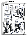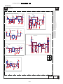
1
Colour Television
Chassis
TPN1.1HA
LA
19020_000_100727.eps
100806
Contents
Page
Revision List
2
Technical Specifications and Connections
2
Precautions, Notes, and Abbreviation List
5
Mechanical Instructions
9
Service Modes, Error Codes, and Fault Finding 14
Alignments
19
Circuit Descriptions
21
IC Data Sheets
24
Block Diagrams
Wiring Diagram 32"
33
Wiring Diagram 37", 42"
34
Block Diagram
35
10. Circuit Diagrams and PWB Layouts
Drawing
Power Board: 32"
(A01) 36
Power Board: 37", 42"
(A01) 39
SSB: D-sub input
(B01) 42
SSB: Rear I/O
(B02) 43
SSB: Scart
(B03) 44
SSB: Scart 2
(B04) 45
SSB: Side input
(B05) 46
SSB: CVBS audio out
(B06) 47
SSB: Tuner
(B07) 48
SSB: HDMI input
(B08) 49
SSB: HDMI input 3
(B09) 50
SSB: Scaler NT7263X
(B10) 51
SSB: DDR memory
(B11) 52
SSB: Panel I/F ICE/UART
(B12) 53
SSB: iTV
(B13) 54
SSB: Key, I/R board
(B14) 55
SSB: USB
(B15) 56
SSB: Scart audio/SPdif out
(B16) 57
SSB: Audio amplifier
(B17) 58
SSB: PSU & Inverter I/F
(B18) 59
SSB: DC-DC Power
(B19) 60
Contents
1.
2.
3.
4.
5.
6.
7.
8.
9.
Page
Keyboard Control Panel
Bathroom Speaker Board
IR/LED Board
11. Styling Sheets
Styling Sheet 32"
Styling Sheet 37"
Styling Sheet 42"
(E) 63
(HS) 65
(J) 68
64
66-67
69
70
71
72
PWB
37-38
40-41
61-62
61-62
61-62
61-62
61-62
61-62
61-62
61-62
61-62
61-62
61-62
61-62
61-62
61-62
61-62
61-62
61-62
61-62
61-62
©
Copyright 2010 Koninklijke Philips Electronics N.V.
All rights reserved. No part of this publication may be reproduced, stored in a
retrieval system or transmitted, in any form or by any means, electronic, mechanical,
photocopying, or otherwise without the prior permission of Philips.
Published by SaS/CC 1068 BU TV Consumer Care, the Netherlands
Subject to modification
EN 3122 785 19020
2010-Aug-13
EN 2
1.
TPN1.1HA LA
Revision List
1. Revision List
Manual xxxx xxx xxxx.0
• First release.
2. Technical Specifications and Connections
2.2
Index of this chapter:
2.1 Technical Specifications
2.2 Directions for Use
2.3 Connections
2.4 Chassis Overview
Directions for use can be downloaded from the following
websites:
http://www.philips.com/support
http://www.p4c.philips.com
Notes:
• Figures can deviate due to the different set executions.
• Specifications are indicative (subject to change).
2.1
Technical Specifications
For on-line product support please use the links in. Here is
product information available, as well as getting started, user
manuals, frequently asked questions and software & drivers.
Table 2-1 Described Model Numbers
Model Number
Styling
Published in
32HFL5332/93
Pro Plus
3122 785 19020
32HFL5332/97
Pro Plus
3122 785 19020
37HFL5382/93
Pro Plus
3122 785 19020
42HFL5382/93
Pro Plus
3122 785 19020
Note: The given Model Numbers are subject to change.
2010-Aug-13
Directions for Use
Technical Specifications and Connections
2.
EN 3
Connections
2W 8
EXT SPKR
OUT
VOL SPKR
SELECT
2.3
TPN1.1HA LA
EXT SPKR
VOL CTRL
1
2
3
4
5
8
7
9
SERIAL
EXPRESS
AV-OUT
AV-IN
11
10
6
BATHROOM
SPEAKER 8
17
16 15
14
13
12
19020_001_100727.eps
100810
Figure 2-1 Connection overview
Note: The following connector colour abbreviations are used
(acc. to DIN/IEC 757): Bk= Black, Bu= Blue, Gn= Green,
Gy= Grey, Rd= Red, Wh= White, Ye= Yellow.
3 - USB2.0
1
2.3.1
2
3
4
10000_022_090121.eps
090121
Side Connections
Figure 2-2 USB (type A)
1 - Mini Jack: EXT speaker (8 Ω / 2 W - Output)
1 - Control Signal
OUT2 - Control Signal
OUT+
3 - Control Signal
OUT+
kq
kq
kq
2 - Mini Jack: EXT speaker volume contro (Input)
1 - Control Signal
IN2 - Control Signal
IN+
jq
jq
1
2
3
4
- +5V
- Data (-)
- Data (+)
- Ground
Gnd
k
jk
jk
H
4 - Head phone (Output)
Bk - Head phone
80 - 600 Ω / 10 mW
ot
5 - Cinch: Audio - In
Ye - Video CVBS
Rd - Audio R
Wh - Audio L
jq
jq
jq
1 VPP / 75 Ω
0.5 VRMS / 10 kΩ
0.5 VRMS / 10 kΩ
2010-Aug-13
EN 4
2.
TPN1.1HA LA
Technical Specifications and Connections
12 - Mini Jack: Bathroom speaker (8 Ω / 1 W - Output)
1 - Control Signal
OUTkq
2 - Control Signal
OUT+
kq
3 - Control Signal
OUT+
kq
6 - HDMI: Digital Video, Digital Audio - In
19
18
1
2
10000_017_090121.eps
090428
Figure 2-3 HDMI (type A) connector
1
2
3
4
5
6
7
8
9
10
11
12
13
14
15
16
17
18
19
20
2.3.2
- D2+
- Shield
- D2- D1+
- Shield
- D1- D0+
- Shield
- D0- CLK+
- Shield
- CLK- n.c.
- n.c.
- DDC_SCL
- DDC_SDA
- Ground
- +5V
- HPD
- Ground
Data channel
Gnd
Data channel
Data channel
Gnd
Data channel
Data channel
Gnd
Data channel
Data channel
Gnd
Data channel
j
H
j
j
H
j
j
H
j
j
H
j
14 - Mini Jack: IR link (Input / Output)
1 - Control Signal
IN
2 - Control Signal
OUT
3 - Ground
Gnd
DDC clock
DDC data
Gnd
Hot Plug Detect
Gnd
j
jk
H
j
j
H
8 - Cinch: S/PDIF - Out
Bk - Coaxial
0.4 - 0.6VPP / 75 ohm
kq
9 - TV ANTENNA - In
Signal input from an antenna, cable or satellite.
10 - Cinch: Audio - In
See 5 - Cinch: Audio - In
11 - Cinch: Audio - Out
Ye - Video CVBS
1 VPP / 75 Ω
Rd - Audio R
0.5 VRMS / 10 kΩ
Wh - Audio L
0.5 VRMS / 10 kΩ
Chassis Overview
Refer to 9. Block Diagrams for PWB/CBA locations.
kq
kq
kq
jq
jq
jq
jq
jq
jq
kq
H
15 - PC IN:VGA
1
Rear Connections
2010-Aug-13
0.5 VRMS / 10 kW
0.5 VRMS / 10 kW
Wh - Audio - L
Rd - Audio - R
6
7 - HDMI1: Digital Video, Digital Audio - In
See 6 - HDMI: Digital Video, Digital Audio - In
2.4
13 - EXT2: Video YPbPr - In, Audio - In
Gn - Video - Y
1 VPP / 75 W
Bu - Video - Pb
0.7 VPP / 75 W
Rd - Video - Pr
0.7 VPP / 75 W
11
5
10
15
10000_002_090121.eps
090127
Figure 2-4 VGA connector
1
2
3
4
5
6
7
8
9
10
11
12
13
14
15
- Video Red
- Video Green
- Video Blue
- n.c.
- Ground
- Ground Red
- Ground Green
- Ground Blue
- +5VDC
- Ground Sync
- Ground Red
- DDC_SDA
- H-sync
- V-sync
- DDC_SCL
0.7 VPP / 75 Ω
0.7 VPP / 75 Ω
0.7 VPP / 75 Ω
j
j
j
Gnd
Gnd
Gnd
Gnd
+5 V
Gnd
Gnd
DDC data
0-5V
0-5V
DDC clock
H
H
H
H
j
H
H
j
j
j
j
16 - Audio - In: Left / Right, VGA
Gn - Audio L/R in
0.5 VRMS / 10 kW
17 - Service / UART
1 - Ground
2 - UART_TX
3 - UART_RX
Gnd
Transmit
Receive
jq
H
k
j
Precautions, Notes, and Abbreviation List
TPN1.1HA LA
3.
EN 5
3. Precautions, Notes, and Abbreviation List
•
Index of this chapter:
3.1 Safety Instructions
3.2 Warnings
3.3 Notes
3.4 Abbreviation List
3.1
Safety Instructions
3.3.2
Safety regulations require that after a repair, the set must be
returned in its original condition. Pay in particular attention to
the following points:
• Route the wire trees correctly and fix them with the
mounted cable clamps.
• Check the insulation of the Mains/AC Power lead for
external damage.
• Check the strain relief of the Mains/AC Power cord for
proper function.
• Check the electrical DC resistance between the Mains/AC
Power plug and the secondary side (only for sets that have
a Mains/AC Power isolated power supply):
1. Unplug the Mains/AC Power cord and connect a wire
between the two pins of the Mains/AC Power plug.
2. Set the Mains/AC Power switch to the “on” position
(keep the Mains/AC Power cord unplugged!).
3. Measure the resistance value between the pins of the
Mains/AC Power plug and the metal shielding of the
tuner or the aerial connection on the set. The reading
should be between 4.5 MΩ and 12 MΩ.
4. Switch “off” the set, and remove the wire between the
two pins of the Mains/AC Power plug.
• Check the cabinet for defects, to prevent touching of any
inner parts by the customer.
•
•
•
•
•
3.3.3
All resistor values are in ohms, and the value multiplier is
often used to indicate the decimal point location (e.g. 2K2
indicates 2.2 kΩ).
Resistor values with no multiplier may be indicated with
either an “E” or an “R” (e.g. 220E or 220R indicates 220 Ω).
All capacitor values are given in micro-farads (μ = × 10-6),
nano-farads (n = × 10-9), or pico-farads (p = × 10-12).
Capacitor values may also use the value multiplier as the
decimal point indication (e.g. 2p2 indicates 2.2 pF).
An “asterisk” (*) indicates component usage varies. Refer
to the diversity tables for the correct values.
The correct component values are listed on the Philips
Spare Parts Web Portal.
Spare Parts
For the latest spare part overview, consult your Philips Spare
Part web portal.
3.3.4
BGA (Ball Grid Array) ICs
Introduction
For more information on how to handle BGA devices, visit this
URL: http://www.atyourservice-magazine.com. Select
“Magazine”, then go to “Repair downloads”. Here you will find
Information on how to deal with BGA-ICs.
BGA Temperature Profiles
For BGA-ICs, you must use the correct temperature-profile.
Where applicable and available, this profile is added to the IC
Data Sheet information section in this manual.
3.3.5
3.2
Schematic Notes
•
Safety regulations require the following during a repair:
• Connect the set to the Mains/AC Power via an isolation
transformer (> 800 VA).
• Replace safety components, indicated by the symbol h,
only by components identical to the original ones. Any
other component substitution (other than original type) may
increase risk of fire or electrical shock hazard.
Where necessary, measure the waveforms and voltages
with (D) and without (E) aerial signal. Measure the
voltages in the power supply section both in normal
operation (G) and in stand-by (F). These values are
indicated by means of the appropriate symbols.
Lead-free Soldering
Warnings
•
•
•
•
3.3
Notes
3.3.1
General
•
Due to lead-free technology some rules have to be respected
by the workshop during a repair:
• Use only lead-free soldering tin. If lead-free solder paste is
required, please contact the manufacturer of your soldering
equipment. In general, use of solder paste within
workshops should be avoided because paste is not easy to
store and to handle.
• Use only adequate solder tools applicable for lead-free
soldering tin. The solder tool must be able:
– To reach a solder-tip temperature of at least 400°C.
– To stabilize the adjusted temperature at the solder-tip.
– To exchange solder-tips for different applications.
• Adjust your solder tool so that a temperature of around
360°C - 380°C is reached and stabilized at the solder joint.
Heating time of the solder-joint should not exceed ~ 4 sec.
Avoid temperatures above 400°C, otherwise wear-out of
tips will increase drastically and flux-fluid will be destroyed.
To avoid wear-out of tips, switch “off” unused equipment or
reduce heat.
• Mix of lead-free soldering tin/parts with leaded soldering
tin/parts is possible but PHILIPS recommends strongly to
avoid mixed regimes. If this cannot be avoided, carefully
clear the solder-joint from old tin and re-solder with new tin.
All ICs and many other semiconductors are susceptible to
electrostatic discharges (ESD w). Careless handling
during repair can reduce life drastically. Make sure that,
during repair, you are connected with the same potential as
the mass of the set by a wristband with resistance. Keep
components and tools also at this same potential.
Be careful during measurements in the high voltage
section.
Never replace modules or other components while the unit
is switched “on”.
When you align the set, use plastic rather than metal tools.
This will prevent any short circuits and the danger of a
circuit becoming unstable.
Measure the voltages and waveforms with regard to the
chassis (= tuner) ground (H), or hot ground (I), depending
on the tested area of circuitry. The voltages and waveforms
shown in the diagrams are indicative. Measure them in the
Service Default Mode with a colour bar signal and stereo
sound (L: 3 kHz, R: 1 kHz unless stated otherwise) and
picture carrier at 475.25 MHz for PAL, or 61.25 MHz for
NTSC (channel 3).
3.3.6
Alternative BOM identification
It should be noted that on the European Service website,
“Alternative BOM” is referred to as “Design variant”.
2010-Aug-13
EN 6
3.
TPN1.1HA LA
Precautions, Notes, and Abbreviation List
The third digit in the serial number (example:
AG2B0335000001) indicates the number of the alternative
B.O.M. (Bill Of Materials) that has been used for producing the
specific TV set. In general, it is possible that the same TV
model on the market is produced with e.g. two different types
of displays, coming from two different suppliers. This will then
result in sets which have the same CTN (Commercial Type
Number; e.g. 28PW9515/12) but which have a different B.O.M.
number.
By looking at the third digit of the serial number, one can
identify which B.O.M. is used for the TV set he is working with.
If the third digit of the serial number contains the number “1”
(example: AG1B033500001), then the TV set has been
manufactured according to B.O.M. number 1. If the third digit is
a “2” (example: AG2B0335000001), then the set has been
produced according to B.O.M. no. 2. This is important for
ordering the correct spare parts!
For the third digit, the numbers 1...9 and the characters A...Z
can be used, so in total: 9 plus 26= 35 different B.O.M.s can be
indicated by the third digit of the serial number.
Identification: The bottom line of a type plate gives a 14-digit
serial number. Digits 1 and 2 refer to the production centre (e.g.
AG is Bruges), digit 3 refers to the B.O.M. code, digit 4 refers
to the Service version change code, digits 5 and 6 refer to the
production year, and digits 7 and 8 refer to production week (in
example below it is 2006 week 17). The 6 last digits contain the
serial number.
3.4
Abbreviation List
0/6/12
AARA
ACI
ADC
AFC
AGC
AM
AP
AR
ASF
ATSC
MODEL
: 32PF9968/10
PROD.NO: AG 1A0617 000001
MADE IN BELGIUM
220-240V ~ 50/60Hz
128W
VHF+S+H+UHF
S
BJ3.0E LA
10000_024_090121.eps
100105
Figure 3-1 Serial number (example)
3.3.7
Board Level Repair (BLR) or Component Level Repair
(CLR)
If a board is defective, consult your repair procedure to decide
if the board has to be exchanged or if it should be repaired on
component level.
If your repair procedure says the board should be exchanged
completely, do not solder on the defective board. Otherwise, it
cannot be returned to the O.E.M. supplier for back charging!
3.3.8
Practical Service Precautions
•
•
ATV
Auto TV
It makes sense to avoid exposure to electrical shock.
While some sources are expected to have a possible
dangerous impact, others of quite high potential are of
limited current and are sometimes held in less regard.
Always respect voltages. While some may not be
dangerous in themselves, they can cause unexpected
reactions that are best avoided. Before reaching into a
powered TV set, it is best to test the high voltage insulation.
It is easy to do, and is a good service precaution.
AV
AVC
AVIP
B/G
BDS
BLR
BTSC
B-TXT
C
CEC
CL
CLR
ComPair
CP
CSM
CTI
CVBS
DAC
DBE
DCM
DDC
D/K
DFI
2010-Aug-13
SCART switch control signal on A/V
board. 0 = loop through (AUX to TV),
6 = play 16 : 9 format, 12 = play 4 : 3
format
Automatic Aspect Ratio Adaptation:
algorithm that adapts aspect ratio to
remove horizontal black bars; keeps
the original aspect ratio
Automatic Channel Installation:
algorithm that installs TV channels
directly from a cable network by
means of a predefined TXT page
Analogue to Digital Converter
Automatic Frequency Control: control
signal used to tune to the correct
frequency
Automatic Gain Control: algorithm that
controls the video input of the feature
box
Amplitude Modulation
Asia Pacific
Aspect Ratio: 4 by 3 or 16 by 9
Auto Screen Fit: algorithm that adapts
aspect ratio to remove horizontal black
bars without discarding video
information
Advanced Television Systems
Committee, the digital TV standard in
the USA
See Auto TV
A hardware and software control
system that measures picture content,
and adapts image parameters in a
dynamic way
External Audio Video
Audio Video Controller
Audio Video Input Processor
Monochrome TV system. Sound
carrier distance is 5.5 MHz
Business Display Solutions (iTV)
Board-Level Repair
Broadcast Television Standard
Committee. Multiplex FM stereo sound
system, originating from the USA and
used e.g. in LATAM and AP-NTSC
countries
Blue TeleteXT
Centre channel (audio)
Consumer Electronics Control bus:
remote control bus on HDMI
connections
Constant Level: audio output to
connect with an external amplifier
Component Level Repair
Computer aided rePair
Connected Planet / Copy Protection
Customer Service Mode
Color Transient Improvement:
manipulates steepness of chroma
transients
Composite Video Blanking and
Synchronization
Digital to Analogue Converter
Dynamic Bass Enhancement: extra
low frequency amplification
Data Communication Module. Also
referred to as System Card or
Smartcard (for iTV).
See “E-DDC”
Monochrome TV system. Sound
carrier distance is 6.5 MHz
Dynamic Frame Insertion
Precautions, Notes, and Abbreviation List
DFU
DMR
DMSD
DNM
DNR
DRAM
DRM
DSP
DST
DTCP
DVB-C
DVB-T
DVD
DVI(-d)
E-DDC
EDID
EEPROM
EMI
EPG
EPLD
EU
EXT
FDS
FDW
FLASH
FM
FPGA
FTV
Gb/s
G-TXT
H
HD
HDD
HDCP
HDMI
HP
I
I2 C
I2 D
I2 S
IF
IR
IRQ
ITU-656
Directions For Use: owner's manual
Digital Media Reader: card reader
Digital Multi Standard Decoding
Digital Natural Motion
Digital Noise Reduction: noise
reduction feature of the set
Dynamic RAM
Digital Rights Management
Digital Signal Processing
Dealer Service Tool: special remote
control designed for service
technicians
Digital Transmission Content
Protection; A protocol for protecting
digital audio/video content that is
traversing a high speed serial bus,
such as IEEE-1394
Digital Video Broadcast - Cable
Digital Video Broadcast - Terrestrial
Digital Versatile Disc
Digital Visual Interface (d= digital only)
Enhanced Display Data Channel
(VESA standard for communication
channel and display). Using E-DDC,
the video source can read the EDID
information form the display.
Extended Display Identification Data
(VESA standard)
Electrically Erasable and
Programmable Read Only Memory
Electro Magnetic Interference
Electronic Program Guide
Erasable Programmable Logic Device
Europe
EXTernal (source), entering the set by
SCART or by cinches (jacks)
Full Dual Screen (same as FDW)
Full Dual Window (same as FDS)
FLASH memory
Field Memory or Frequency
Modulation
Field-Programmable Gate Array
Flat TeleVision
Giga bits per second
Green TeleteXT
H_sync to the module
High Definition
Hard Disk Drive
High-bandwidth Digital Content
Protection: A “key” encoded into the
HDMI/DVI signal that prevents video
data piracy. If a source is HDCP coded
and connected via HDMI/DVI without
the proper HDCP decoding, the
picture is put into a “snow vision” mode
or changed to a low resolution. For
normal content distribution the source
and the display device must be
enabled for HDCP “software key”
decoding.
High Definition Multimedia Interface
HeadPhone
Monochrome TV system. Sound
carrier distance is 6.0 MHz
Inter IC bus
Inter IC Data bus
Inter IC Sound bus
Intermediate Frequency
Infra Red
Interrupt Request
The ITU Radio communication Sector
(ITU-R) is a standards body
subcommittee of the International
Telecommunication Union relating to
radio communication. ITU-656 (a.k.a.
ITV
LS
LATAM
LCD
LED
L/L'
LPL
LS
LVDS
Mbps
M/N
MHEG
MIPS
MOP
MOSFET
MPEG
MPIF
MUTE
MTV
NC
NICAM
NTC
NTSC
NVM
O/C
OSD
OAD
OTC
P50
PAL
TPN1.1HA LA
3.
EN 7
SDI), is a digitized video format used
for broadcast grade video.
Uncompressed digital component or
digital composite signals can be used.
The SDI signal is self-synchronizing,
uses 8 bit or 10 bit data words, and has
a maximum data rate of 270 Mbit/s,
with a minimum bandwidth of 135
MHz.
Institutional TeleVision; TV sets for
hotels, hospitals etc.
Last Status; The settings last chosen
by the customer and read and stored
in RAM or in the NVM. They are called
at start-up of the set to configure it
according to the customer's
preferences
Latin America
Liquid Crystal Display
Light Emitting Diode
Monochrome TV system. Sound
carrier distance is 6.5 MHz. L' is Band
I, L is all bands except for Band I
LG.Philips LCD (supplier)
Loudspeaker
Low Voltage Differential Signalling
Mega bits per second
Monochrome TV system. Sound
carrier distance is 4.5 MHz
Part of a set of international standards
related to the presentation of
multimedia information, standardised
by the Multimedia and Hypermedia
Experts Group. It is commonly used as
a language to describe interactive
television services
Microprocessor without Interlocked
Pipeline-Stages; A RISC-based
microprocessor
Matrix Output Processor
Metal Oxide Silicon Field Effect
Transistor, switching device
Motion Pictures Experts Group
Multi Platform InterFace
MUTE Line
Mainstream TV: TV-mode with
Consumer TV features enabled (iTV)
Not Connected
Near Instantaneous Compounded
Audio Multiplexing. This is a digital
sound system, mainly used in Europe.
Negative Temperature Coefficient,
non-linear resistor
National Television Standard
Committee. Color system mainly used
in North America and Japan. Color
carrier NTSC M/N= 3.579545 MHz,
NTSC 4.43= 4.433619 MHz (this is a
VCR norm, it is not transmitted off-air)
Non-Volatile Memory: IC containing
TV related data such as alignments
Open Circuit
On Screen Display
Over the Air Download. Method of
software upgrade via RF transmission.
Upgrade software is broadcasted in
TS with TV channels.
On screen display Teletext and
Control; also called Artistic (SAA5800)
Project 50: communication protocol
between TV and peripherals
Phase Alternating Line. Color system
mainly used in West Europe (color
carrier= 4.433619 MHz) and South
America (color carrier PAL M=
2010-Aug-13
EN 8
3.
PCB
PCM
PDP
PFC
PIP
PLL
POD
POR
PSDL
PSL
PSLS
PTC
PWB
PWM
QRC
QTNR
QVCP
RAM
RGB
RC
RC5 / RC6
RESET
ROM
RSDS
R-TXT
SAM
S/C
SCART
SCL
SCL-F
SD
SDA
SDA-F
SDI
SDRAM
SECAM
SIF
SMPS
SoC
SOG
SOPS
SPI
S/PDIF
SRAM
SRP
SSB
SSC
STB
STBY
SVGA
2010-Aug-13
TPN1.1HA LA
Precautions, Notes, and Abbreviation List
3.575612 MHz and PAL N= 3.582056
MHz)
Printed Circuit Board (same as “PWB”)
Pulse Code Modulation
Plasma Display Panel
Power Factor Corrector (or Preconditioner)
Picture In Picture
Phase Locked Loop. Used for e.g.
FST tuning systems. The customer
can give directly the desired frequency
Point Of Deployment: a removable
CAM module, implementing the CA
system for a host (e.g. a TV-set)
Power On Reset, signal to reset the uP
Power Supply for Direct view LED
backlight with 2D-dimming
Power Supply with integrated LED
drivers
Power Supply with integrated LED
drivers with added Scanning
functionality
Positive Temperature Coefficient,
non-linear resistor
Printed Wiring Board (same as “PCB”)
Pulse Width Modulation
Quasi Resonant Converter
Quality Temporal Noise Reduction
Quality Video Composition Processor
Random Access Memory
Red, Green, and Blue. The primary
color signals for TV. By mixing levels
of R, G, and B, all colors (Y/C) are
reproduced.
Remote Control
Signal protocol from the remote
control receiver
RESET signal
Read Only Memory
Reduced Swing Differential Signalling
data interface
Red TeleteXT
Service Alignment Mode
Short Circuit
Syndicat des Constructeurs
d'Appareils Radiorécepteurs et
Téléviseurs
Serial Clock I2C
CLock Signal on Fast I2C bus
Standard Definition
Serial Data I2C
DAta Signal on Fast I2C bus
Serial Digital Interface, see “ITU-656”
Synchronous DRAM
SEequence Couleur Avec Mémoire.
Color system mainly used in France
and East Europe. Color carriers=
4.406250 MHz and 4.250000 MHz
Sound Intermediate Frequency
Switched Mode Power Supply
System on Chip
Sync On Green
Self Oscillating Power Supply
Serial Peripheral Interface bus; a 4wire synchronous serial data link
standard
Sony Philips Digital InterFace
Static RAM
Service Reference Protocol
Small Signal Board
Spread Spectrum Clocking, used to
reduce the effects of EMI
Set Top Box
STand-BY
800 × 600 (4:3)
SVHS
SW
SWAN
SXGA
TFT
THD
TMDS
TS
TXT
TXT-DW
UI
uP
UXGA
V
VESA
VGA
VL
VSB
WYSIWYR
WXGA
XTAL
XGA
Y
Y/C
YPbPr
YUV
Super Video Home System
Software
Spatial temporal Weighted Averaging
Noise reduction
1280 × 1024
Thin Film Transistor
Total Harmonic Distortion
Transmission Minimized Differential
Signalling
Transport Stream
TeleteXT
Dual Window with TeleteXT
User Interface
Microprocessor
1600 × 1200 (4:3)
V-sync to the module
Video Electronics Standards
Association
640 × 480 (4:3)
Variable Level out: processed audio
output toward external amplifier
Vestigial Side Band; modulation
method
What You See Is What You Record:
record selection that follows main
picture and sound
1280 × 768 (15:9)
Quartz crystal
1024 × 768 (4:3)
Luminance signal
Luminance (Y) and Chrominance (C)
signal
Component video. Luminance and
scaled color difference signals (B-Y
and R-Y)
Component video
Mechanical Instructions
TPN1.1HA LA
4.
EN 9
4. Mechanical Instructions
Index of this chapter:
4.1 Cable Dressing
4.2 Service Positions
4.3 Assembly/Panel Removal
4.4 Set Re-assembly.
4.1
Notes:
• Figures below can deviate slightly from the actual situation,
due to the different set executions.
Cable Dressing
19020_100_100727.eps
100806
Figure 4-1 Cable dressing (32")
2010-Aug-13
EN 10
4.
TPN1.1HA LA
Mechanical Instructions
19020_101_100727.eps
100727
Figure 4-2 Cable dressing (37")
2010-Aug-13
Mechanical Instructions
TPN1.1HA LA
4.
EN 11
19020_102_100727.eps
100727
Figure 4-3 Cable dressing (42")
4.2
Service Positions
For easy servicing of a TV set, the set should be put face down
on a soft flat surface, foam buffers or other specific workshop
tools. Ensure that a stable situation is created to perform
measurements and alignments. When using foam bars take
care that these always support the cabinet and never only the
display. Caution: Failure to follow these guidelines can
seriously damage the display!
Ensure that ESD safe measures are taken.
4.3
Assembly/Panel Removal
Instructions below apply to the 32HFL5332/xx, but will be
similar for other models.
4.3.1
Rear Cover
Warning: Disconnect the mains power cord before removing
the rear cover.
Refer to Figure 4-4 for details.
1. Remove fixation screws that secure the rear cover.
2. Lift the rear cover from the TV. Make sure that wires and
flat foils are not damaged while lifting the rear cover from
the set.
2010-Aug-13
EN 12
4.
Mechanical Instructions
TPN1.1HA LA
3
3
4
4
3
3
2×7
1
M3 × 9
2
M4 × 16
3
4
4
4 × 18
1
3
3
1
4
2
4
4
4
4
4
4
19020_103_100806.eps
100811
Figure 4-4 Rear Cover
4.3.2
Small Signal Board (SSB)
Caution: it is mandatory to remount all different screws at their
original position during re-assembly. Failure to do so may result
in damaging the SSB.
1. Release the tape near the bottom side of the set from the
TV panel and release the tape near the left side of the set
from the shielding.
2. Remove the fixation screw near the HDMI side inputs.
3. Remove all other fixation screws from the SSB.
4. Remove the shielding from the SSB.
5. Release the clips from the LVDS connector.
Caution: be careful, as these are very fragile connectors!
6. Release the other cables from their clamps.
7. Unplug all other connectors.
8. Take the SSB out.
Caution: be careful not to damage the thermal pad at the
bottom side of the SSB.
4.3.3
Bathroom Speaker board
Caution: it is mandatory to remount all different screws at their
original position during re-assembly. Failure to do so may result
in damaging the bathroom speaker board.
1. Release the cable from their clamps.
2. Unplug all connectors from the bathroom speaker board.
3. Remove all fixation screws from the bathroom speaker
board.
4. The bathroom speaker board can now be taken out of the
set.
When defective, replace the whole unit.
2010-Aug-13
4.3.4
Power Supply Unit (PSU)
Caution: it is mandatory to remount all different screws at their
original position during re-assembly. Failure to do so may result
in damaging the PSU.
1. Release the Power board cables from their clamps.
2. Unplug power connectors from the SSB and LCD panel.
3. Remove all fixation screws from the PSU.
4. The PSU can now be taken out of the set.
When defective, replace the whole unit.
4.3.5
Stand removal
Caution: it is mandatory to remount all different screws at their
original position during re-assembly. Be sure to put the set in
the Service Position.
1. Remove the fixation screws.
2. Take the stand out.
4.3.6
Speakers
1. Remove the stand as described earlier.
2. Unplug the speaker connector from the SSB.
3. Release the tape near the bottom middle side of the panel
from the TV bezel.
4. Remove all fixation screws from the speaker.
5. Take the speakers out.
When defective, replace the whole unit.
Mechanical Instructions
4.3.7
IR/LED Board
1. Remove the fixation screw.
2. Take the board out from the bezel and unplug the
connector from the IR/LED board.
When defective, replace the whole unit.
4.3.8
Keyboard Control Panel
1. Unplug the connector on the keyboard control panel.
2. Take the keyboard control panel from the bezel.
When defective, replace the whole unit.
4.3.9
4.4
TPN1.1HA LA
4.
EN 13
Set Re-assembly
To re-assemble the whole set, execute all processes in reverse
order.
Notes:
• While re-assembling, make sure that all cables are placed
and connected in their original position.
See Figure 4-1, Figure 4-2 and Figure 4-3.
• Pay special attention not to damage the EMC foams on the
SSB shields. Ensure that EMC foams are mounted
correctly.
LCD Panel
1.
2.
3.
4.
5.
6.
Remove the SSB as described earlier.
Remove the bathroom speaker board as described earlier.
Remove the PSU as described earlier.
Remove the stand as described earlier.
Remove the speaker as described earlier.
Release the control board cable from its clamps and
unplug the control board cable from the control board.
7. Remove the fixation screws that secure the LCD panel with
the metal bracket.
8. Lift the LCD Panel from the bezel.
When defective, replace the whole unit.
2010-Aug-13
EN 14
5.
TPN1.1HA LA
Service Modes, Error Codes, and Fault Finding
5. Service Modes, Error Codes, and Fault Finding
Index of this chapter:
5.1 Service Modes
5.2 Service Tools
5.3 TV Main Software Upgrading
5.4 Error Codes
5.5 Fault Finding and Repair Tips
5.1
Service Modes
The Customer Service Mode (CSM) is used for communication
between the call centre and the customer, while the Service
Alignment Mode (SAM) offers several features for the service
technician.
This chassis also offers the option of using ComPair, a
hardware interface between a computer and the TV chassis. It
offers the abilities of structured troubleshooting, error code
reading, and software version read-out for all chassis.
5.1.1
19020_201_100727.eps
100727
Figure 5-2 CSM Menu [2/3]
Customer Service Mode (CSM)
Purpose
The Customer Service Mode shows error codes and
information on the TV's operation settings.The call centre can
instruct the customer (by telephone) to enter CSM in order to
identify the status of the set.This helps the call centre to
diagnose problems and failures in the TV set before making a
service call.
The CSM is a read-only mode; therefore, modifications are not
possible in this mode.
How to Activate CSM
Key in the code “123654” via the standard RC transmitter.
19020_202_100727.eps
100727
Note: Activation of the CSM is only possible if there is no (user)
menu on the screen!
Figure 5-3 CSM Menu [3/3]
How to Navigate
By means of the “CURSOR-DOWN/UP” knob (or the scroll
wheel) on the RC-transmitter, can be navigated through the
menus.
19020_200_100727.eps
100727
Figure 5-1 CSM Menu [1/3]
2010-Aug-13
General
• 1.1 Set Type NVM read/write (max. 16 characters).
• 1.2 Production code NVM read/write (max. 16
characters).
• 1.3 Reserved Not applicable.
• 1.4 Option Code Store in NVM (set feature grouping as
option) panel code.
• 1.5 Codes Error code Layer 2. Store in NVM. 10 error
buffers: 000 = No problem, 011 = I2C bus error,
012 = tuner error, 013 = panel.
• 1.6 SSB 12NC NVM read/write (12 characters).
• 1.7 Display 12NC NVM read/write (12 characters).
• 1.8 PSU 12NC NVM read/write (12 characters).
• 2.1 Current Main SW Detects and displays software
version.
• 2.2 Reserved Not applicable.
• 2.3 Reserved Not applicable.
• 2.4 NVM-version Detects and displays software version.
• 3.1 Signal Quality/Present analog/digital signal strength.
• 3.2 TV lock Detects and displays.
• 3.3 HDCP key Detects and displays.
• 3.4 Reserved Not applicable.
• 3.5 Reserved Not applicable.
• 3.6 HDMI audio format input Per supported format e.g.
Dolby TrueHD, DTS-HD Master Audio, MPCM.
Service Modes, Error Codes, and Fault Finding
•
TPN1.1HA LA
5.
EN 15
3.7 HDMI video format input Per Supported format. e.g.
576i 50 Hz, 576p 50 Hz, 720p 50 Hz, 1080i 50 Hz,
1080p 50 Hz
How to Exit CSM
Press “MENU” on the RC-transmitter.
5.1.2
Service Alignment Mode (SAM)
How to enter
To enter the factory mode, use the following method:
• Press the following key sequence on the remote control
transmitter: “MENU 1 9 9 9”.
After entering the factory mode, the following screen is visible
on the top and right of the panel.
How to Navigate
With the up/down cursor keys can be used to navigate through
the menu, while with the Left/Right cursor the values can be
changed.
How to EXIT
Choose “EXIT”, and press the “OK” button.
Notes: (only applicable to xxHFL5332/93)
• When the Hotel mode is active, the service modes CSM,
SDM, SAM and ComPair are automatically disabled (this is
to prevent hotel guests entering Philips service modes).
• In order to use the service modes and ComPair, Hotel
mode must be disabled.
• To enable/disable the hotel mode, the hotel setup remote
(green remote) is needed.
19020_203_100727.eps
100727
Figure 5-4 Example of SAM
Table 5-1 Contents of SAM
Action Items
Range
Default Value
Description
32"
37"
42"
Brand
PHILIPS
PHILIPS
PHILIPS
Ver
TPN11HA_1.12
TPN11HA_1.12
TPN11HA_1.12
brand customer
software version
Date
Jul 14 2010
Jul 14 2010
Jul 14 2010
Model name
32HFL5332/93
37HFL5382/93
42HFL5382/93
software release date
model name
Scaler
NT72634
NT72634
NT72634
scaler IC type
Panel type
V315B5-L02(125)
LC370WUN-SCC1(126)
LC420WUN-SCB1(127) panel type and display code
Current source
TV
TV
TV
select source
Auto color
GO
GO
GO
PC: any pattern has black and white YPbPr: SMPTEbar (colour bar), any
timing.
ADC offset
0 - 255
R0 G0 B0
R0 G0 B0
R0 G0 B0
PC: any pattern has black and white YPbPr: SMPTEbar (colour bar), any
timing.
ADC gain
0 - 255
R0 G0 B0
R0 G0 B0
R0 G0 B0
PC: any pattern has black and white YPbPr: SMPTEbar (colour bar), any
timing.
Normal
Normal
Color temp
Scaler offset
0 - 255
R 128
G 128 B 128 R 128
Scaler gain
0 - 255
R 127 G 124
B121
R 127
Normal
colour temperature, normal, cool, warm
G 128
B 128
R 128
G 128 B 128
G 126
B117
R 127 G 128 B123
Back-End Scaler R G B Gain NVM has YPbPr NORMAL, WARM, COOL,
CUSTOMER four sets. Other source use offset with hardcoding
Back-End Scaler R G B Gain NVM has YPbPr NORMAL, WARM, COOL,
CUSTOMER four sets. Other source use offset with hardcoding
Burn in
Off
Off
Off
Puts the set in Burn In mode, for factory use only
EEPROM init
GO
GO
GO
resets the EEPROM to initial mode
Backlight time
x hours
x hours
x hours
the set backlight running time
Error code
000 000 000 000 000
000 000 000 000 000
000 000 000 000 000
error code layer 2. Store in NVM.
Clear error code
GO
GO
GO
clears error code Layer 2. in NVM.
Reset PBS setting
GO
GO
GO
resets the PBS setting
Virgin mode
Off
Off
Off
resets the set to manufacturer's mode
ACI
On
On
On
ACI on or off
ATS
On
On
On
ATS on or off
NVM address
NVM address
0×0 (0)
0×0 (0)
0×0 (0)
NVM value
0×7B (123)
0×7B (123)
0×7B (123)
NVM value NVM
NVM copy to USB
GO
GO
GO
use this to copy the NVM data from the TV to the USB
GO
GO
GO
use this to restore the NVM data from the USB to the TV
NVM paste from USB
Exit
Press OK
Exit from factory mode
2010-Aug-13
EN 16
5.1.3
5.
Service Modes, Error Codes, and Fault Finding
TPN1.1HA LA
Caution: It is compulsory to connect the TV to the PC as
shown in the picture above (with the ComPair interface in
between), as the ComPair interface acts as a level shifter. If
one connects the TV directly to the PC (via UART), ICs will be
damaged!
Hotel mode
Notes: (only applicable to xxHFLxxxxX/nn)
• Refer to the user manual for more information on the hotel
mode.
• When in the hotel mode, the service modes CSM, SDM,
SAM and ComPair are automatically disabled (this is to
prevent hotel guests entering Philips service modes).
• In order to use the service modes and ComPair, hotel
mode must be disabled.
• To enable/disable the hotel mode, the hotel setup remote
(green remote) is needed.
5.2
Service Tools
5.2.1
ComPair
How to Order
ComPair II order codes:
• ComPair II interface: 3122 785 90630.
• Programming software can be downloaded from the Philips
Service portal.
• ComPair UART interface cable for TPN1.1HA xx.
3122 785 90630.
Note: While having problems, contact the local support desk.
Introduction
ComPair (Computer Aided Repair) is a Service tool for Philips
Consumer Electronics products. and offers the following:
1. ComPair helps to quickly get an understanding on how to
repair the chassis in a short and effective way.
2. ComPair allows very detailed diagnostics and is therefore
capable of accurately indicating problem areas. No
knowledge on I2C or UART commands is necessary,
because ComPair takes care of this.
3. ComPair speeds up the repair time since it can
automatically communicate with the chassis (when the uP
is working) and all repair information is directly available.
4. ComPair features TV software upgrade possibilities.
Specifications
ComPair consists of a Windows based fault finding program
and an interface box between PC and the (defective) product.
The ComPair II interface box is connected to the PC via an
USB cable. For the TV chassis, the ComPair interface box and
the TV communicate via a bi-directional cable via the service
connector(s).
The ComPair fault finding program is able to determine the
problem of the defective television, by a combination of
automatic diagnostics and an interactive question/answer
procedure.
5.3
TV Main Software Upgrading
5.3.1
Introduction
Philips continuously tries to improve its products, and we
recommend that you update the TV software when updates are
available. Software update files can be obtained from your
dealer or can be downloaded from the Philips servicer network
web site (P4S).
Preparing a portable memory for software upgrade
You require the following:
1. A personal computer connected to the Internet.
2. An archive utility that supports the ZIP-format (e.g. WinZip
for Windows or Stufflt for Mac OS).
3. A USB flash drive (preferably empty).
Note:
1. Only FAT/DOS-formatted flash drives are supported.
2. Only use software update files that can be found on the
Philips servicer network web site (P4S).
5.3.2
Before starting the software upgrade procedure, it is advised to
check that what the current TV software:
1. Press the “Menu” button on your remote control.
2. Select “Setup” and press “OK”, then select [Software
update] > [Current software].
If the current software version of your TV is the same as the
latest update file found on the Philips servicer network web site
(P4S), it is not necessary to update the TV software.
How to Connect
This is described in the chassis fault finding database in
ComPair.
TO TV
TO
UART SERVICE
CONNECTOR
ComPair II
RC in
RC out
TO
I2C SERVICE
CONNECTOR
TO
UART SERVICE
CONNECTOR
5.3.3
I2C
RS232 /UART
PC
5.3.4
ComPair II Developed by Philips Brugge
HDMI
I2C only
Optional power
5V DC
10000_036_090121.eps
091118
Figure 5-5 ComPair II interface connection
2010-Aug-13
Download the latest software
1. Find the Philips servicer network web site (P4S).
2. Find information and software related to your TV.
3. Select the latest software update file and download it to
your PC.
4. Insert a USB flash drive into one of the USB ports of your
PC.
5. Decompress the downloaded ZIP file and copy the
“autorun.upg” to the root directory of the USB flash drive.
Multi
function
Optional Power Link/ Mode
Switch
Activity
Check the current TV software version
Update the TV software
1. Switch off your TV.
2. Insert the USB flash drive that contains the software
update file.
3. Switch on your TV.
4. Press MENU on the remote control.
5. Select [PBS Settings] > [Consumer Setup] > [Yes] and
press OK. See Figure 5-6.
6. In next menu select [Software update] > [Local updates] >
[USB] and press OK. See Figure 5-7.
Service Modes, Error Codes, and Fault Finding
TPN1.1HA LA
5.
EN 17
7. Select [AUTORUN.UPG] and press OK on the remote
control. See Figure 5-8.
8. When prompted, select [Cancel] or [Update] and press OK.
See Figure 5-9.
9. To proceed, In next menu select [Start] and press OK to
start software updates. See Figure 5-10.
10. Upgrading will now begins and the status of the updating
progress will be displayed.
11. When the TV software is updated, select [Restart] and
press OK to retart the TV. See Figure 5-11.
19020_206_100729.eps
100729
Figure 5-9 Update the TV software 4
19020_213_100809.eps
100809
Figure 5-6 Update the TV software 1
19020_207_100729.eps
100729
Figure 5-10 Update the TV software 5
19020_204_100729.eps
100809
Figure 5-7 Update the TV software 2
19020_208_100729.eps
100729
Figure 5-11 Update the TV software 6
19020_205_100729.eps
100729
Figure 5-8 Update the TV software 3
Note:
• Do not remove the USB flash drive during the software
update.
• If a power failure occurs during the update, do not remove
the USB flash drive from the TV. The TV will continue the
software update as soon as power comes back.
• If an error occurs during the update retry the procedure or
contact your dealer.
• We do not recommend downgrading to an older version.
• Once the upgrade is finished, use your PC to remove the
TV software from your USB portable memory.
2010-Aug-13
EN 18
5.4
5.
TPN1.1HA LA
Service Modes, Error Codes, and Fault Finding
Error Codes
The error code buffer contains all errors detected since the last
time the buffer was erased. The buffer is written from left to
right. When an error occurs that is not yet in the error code
buffer, it is displayed at the left side and all other errors shift one
position to the right.
Basically there are three kinds of error codes:
Error Code
Event
000
No problem
011
I2C bus error
012
Tuner error
013
panel
5.5
Fault Finding and Repair Tips
5.5.1
Speakers
Make sure that the volume is set to minimum during
disconnecting the speakers in the ON-state of the TV. The
audio amplifier can be damaged by disconnecting the speakers
during ON-state of the set!
5.5.2
Tuner
Attention: In case the tuner is replaced, always check the tuner
options.
2010-Aug-13
Alignments
TPN1.1HA LA
6.
EN 19
6. Alignments
Process
1. Press the following key sequence on the remote control
transmitter: “MENU 1 9 9 9”, see Figure 6-2.
2. Press B, y to move cursor to “Auto Color”.
3. Press Go to do “ADC Gain” and “ADC Offset”.
4. “Exit”.
Index of this chapter:
6.1 General Alignment Conditions
6.2 Hardware Alignments
6.3 Auto Colour for ADC Calibration
6.4 White Balance Adjustment
6.5 Option Settings
Note: The Service Alignment Mode (SAM) are described in
chapter 5. Service Modes, Error Codes, and Fault Finding.
Menu navigation is done with the CURSOR UP, DOWN, LEFT
or RIGHT keys of the remote control transmitter.
6.1
General Alignment Conditions
Perform all electrical adjustments under the following
conditions:
• Power supply voltage: 195 - 264 VAC, 50/60 Hz ± 3 Hz.
• Connect the set to the mains via an isolation transformer
with low internal resistance.
• Allow the set to warm up for approximately 15 minutes.
• Measure voltages and waveforms in relation to correct
ground.
Caution: It is not allowed to use heatsinks as ground.
• Test probe: Ri > 10 MΩ, Ci < 20 pF.
• Use an isolated trimmer/screwdriver to perform
alignments.
6.2
Current Source : CVI
Auto Color
: Go
ADC Offset
: R xxx G xxx B xxx
ADC Gain
: R xxx G xxx B xxx
Color Temp
: Normal
Scaler Offset : R 128 G 128 B 128
Scaler Gain
: R xxx G xxx B xxx
…
Exit
Note: xxx is digit number
19020_209_100729.eps
100729
Figure 6-2 OSD in factory mode
6.3.2
For VGA (R/G/B) source
Requirement:
1. Use Chroma 2226 or equivalent equipments.
2. Set Timing mode at 1360 × 768 at 60 Hz.
3. Apply SMPTE-133 pattern, see Figure 6-1. step 1 =
Black (0% gray level); step 2 = White (100% gray level).
Hardware Alignments
Not applicable.
Process
1. Enter factory mode, then refer to Figure 6-2.
6.3
Auto Colour for ADC Calibration
6.3.1
For EXT2(Y/Pb/Pr) source
6.4
White Balance Adjustment
Equipment requirements:
Use QuantumData 802BT or equivalent equipments.
6.4.1
General set-up
Equipment requirements:
QuantumData 802BT and CS-200/1000.
Input requirements:
Input Signal Type: YPbPr signal
• Set Timing mode at 720p 50 mode.
Input requirements:
Flat (100% gray level, Full White Pattern).
Pattern:
Apply SMPTE133 Pattern, see Figure 6-1.
Input signal timing:
720p 50.
Input Injection Point:
YPbPr input (EXT 2).
Warm-up time:
60 ~ 120 mins @ 25 °C.
Note: The test pattern must always keep same, as well as
pattern generation and timing, to avoid “Dynamic Contrast” and
“Dynamic Backlight” activited at unknown condition. These
parameters are located at “Dig. CrystalClear” of OSD.
6.4.2
18860_204_100507.eps
100806
Figure 6-1 SMPTE133 pattern
Alignment Request in the centre of the screen
Pre-check panel uniformity is OK and Pre-check “White
Original Surface Luminance”, Scaler R/G/B gain = 127.
• 32" panel: > 360 cd/m2.
• 37" panel: > 400 cd/m2.
• 42" panel: > 400 cd/m2.
Adjusting “Scaler Gain” in factory mode. The R/G/B gain value
should be below 127 to avoid saturation at the 11-step grey
pattern.
2010-Aug-13
EN 20
6.
Alignments
TPN1.1HA LA
This group setting of color temp. will be applied automatically in
TV / EXT1/VGA/ HDMI / AV source.
Table 6-1 The 1931 CIE chromaticity (x, y) by CA-210
Picture Mode
x
y
Normal (9000K)
0.286 ± 0.010
0.296 ± 0.010
Cool (11000K)
0.273 ± 0.010
0.283 ± 0.010
Warm (6500K)
0.312 ± 0.010
0.326 ± 0.010
If you do not have a colour analyser, you can use the default
values. This is the next best solution. The default values are
average values coming from production.
• Select a COLOUR TEMPERATURE (e.g. COOL,
NORMAL, or WARM).
• Set the RED, GREEN and BLUE default values according
to the values in Table 6-2
• When finished press OK on the RC, then press STORE (in
the SAM root menu) to store the aligned values to the NVM.
• Restore the initial picture settings after the alignments.
Table 6-2 White tone default settings
Colour temperature
Picture Mode
Normal
Cool
Warm
6.5
Option Settings
6.5.1
Reset Options
Size
Red
Green
Blue
32"
127
124
121
37"
127
126
117
42"
127
127
123
32"
121
121
127
37"
125
127
127
42"
121
125
127
32"
127
120
102
37"
127
118
97
42"
127
117
98
In SAM, after reset “Reset option code”, the set immediately
restarts.
Table 6-3 Display code overview
6.5.2
CTN_ALT BOM#
Panel Type
Panel ID
32HFL5332/93
CMO V315B5-L02
125
32HFL5332/97
CMO V315B5-L02
125
37HFL5382/93
LG LC370WUN-SCC1 126
42HFL5382/93
LG LC420WUN-SCB1 127
Blind SAM mode
In the blind SAM-mode the display option code of the set can
be entered. Use RC command “0 6 2 5 9 8 <MENU> n n n”,
where “n n n” is the display option code, see Table 6-3. Upon
activating the Blind SAM mode, service technician needs to
makesure the CTN and serial number are correctly set inside
the TV set (CSM) as per the family sheet sticker on rear cover.
2010-Aug-13
Circuit Descriptions
TPN1.1HA LA
7.
EN 21
7. Circuit Descriptions
7.1
Index of this chapter:
7.1 Introduction
7.2 Power Architecture
Introduction
The TPN1.1HA LA chassis is using the NT72634 for main
processing.
Notes:
• Only new circuits (circuits that are not published recently)
are described.
• Figures can deviate slightly from the actual situation, due
to different set executions.
• For a good understanding of the following circuit
descriptions, please use the wiring, block (see chapter
9. Block Diagrams) and circuit diagrams (see chapter
10. Circuit Diagrams and PWB Layouts).Where necessary,
you will find a separate drawing for clarification.
7.1.1
TPN1.1HA Architecture Overview
An overview of the TPN1.1HA LA architecture can be found in
Figure 7-1.
SPI Flash
32Mb
24C32
NVM
24C02
DSUB
24C02
HDMI
DDR2
512Mb
HD panel
TV_SIF
SIF+
HD (8 bit)
LVDS Out
TV_CVBS
CVBS_0
HDMI1
HDMI
SWITCH
SIDE HDMI
R/L
HDMI
N T 7 2 63 4
LQFP-256
ADIN_3
Audio amp.
I2S
R/G/B/H/V
VGA_IN
Y/Pb/Pr; R/L
YPbPr_0
ADIN_2
H/Phone amp.
DAC_OUT
• Keypad
R x /T x
UART
• IR / LED
ADC
IR LINK
GPIO
4 pin connection
to Bathroom
speaker board
CVBS_out & Aud_RL_out
CVBS; R/L (rear)
SCART1_Y
CVBS; R/L (Side)
CVBS_1
• Compare
• BUH-L1
1w mono
audio amp
Bathroom
speaker
ADIN_1
ADIN_4
D+/DUSB INT
19020_210_100729.eps
100810
Figure 7-1 Architecture of TPN1.1HA LA
2010-Aug-13
EN 22
7.1.2
7.
TPN1.1HA LA
Circuit Descriptions
SSB Cell Layout
DC/DC
DDR MEMORY
EEPROM
NT72634
DIGITAL I/O
AUDIO CLASS - D
TUNER
ANALOG I/O
NAND FLASH
HDMI SWITCH
ANALOG I/O
HDMI EDID
DIGITAL I/O
SERVICE
CONNECTOR
DIGITAL I/O
HDMI 1 EDID
19020_211_100730.eps
100809
Figure 7-2 SSB layout cells (top view)
2010-Aug-13
Circuit Descriptions
7.2
TPN1.1HA LA
7.
EN 23
Power Architecture
Refer to figure Figure 7-3 for the power architecture of this
platform (DC/DC power conversion).
+5V_STBY
+3.3V_STBY
G903T63UF
G912T63U
U7204
U7203
VDD1V2_STBY
FLASH
U4205
NVT72633
SC189
U7209
SI4835
Q7106
+1V2_ON
U4101
+3V3_ON
+5V_ON
G5657F
U7210
SYSTEM_PWR_EN
24C02
U1101
U5102
U5103
AP1084D
U7205
G1084
U7201
TUNER
TU1601
TU1602
1V8_NT
DDR2
U4201
U4202
Audio OP
U1401
U1501
U6202
+24V_16V_SW
+24V_16V
SI4836
Q6102
AD82581B
U6203
HDMI SW
U5101
18V_PWR_SW
M24C32
U4102
+12V
G5657F
U7211
+5V
PANEL_ON
Panel
FOR PANEL POWER 5V
19020_212_100730.eps
100809
Figure 7-3 Power Architecture
7.2.1
Power Supply Unit
All power supplies are a black box for Service. When defective,
a new board must be ordered and the defective one must be
returned, unless the main fuse of the board is broken. Always
replace a defective fuse with one with the correct
specifications! This part is available in the regular market.
Consult the Service website for the order codes of the boards.
The output voltages to the chassis are:
• +5-STANDBY (stand-by-mode only)
• +12V (panel-on)
• +24V (audio power)
2010-Aug-13
EN 24
8.
TPN1.1HA LA
IC Data Sheets
8. IC Data Sheets
This section shows the internal block diagrams and pin
configurations of ICs that are drawn as “black boxes” in the
electrical diagrams (with the exception of “memory” and “logic”
ICs).
8.1
Diagram B10 SSB: Scaler NT7263X, NT72634FG/A LQFP-256 (IC U4101)
Block diagram
USB Flash
Motion
Picture
Decoder
VGA,
YPbPr
ADC
CVBS,
Y/C
ADC
HDMI
TMDS RX
Visual
Effect
Processor
USB Host
Deinterlace
Video
Decoder
Input
Processor
Display
Processor
LVDS TX
LVDS
TV DAC
CVBS
Noise
Reduction
DRAM
Controller
DDR2
I 2S
Inp ut
L/R
Audio ADC
Audio DSP
SIF
SIF ADC
TV Sound
Decoder
HS,VS
CEC,IR
Standby
Controller
SARADC
ARM9 CPU
Buttons
SPI Flash
Audio DAC
L/R
I2S Output,
S/PDIF
19020_300_100730.eps
100810
Figure 8-1 Internal block diagram
2010-Aug-13
IC Data Sheets
TPN1.1HA LA
8.
EN 25
Pinning information
No
Name
No
Name
No
Name
No
Name
1
MDQ1
65
Ground
129
AUD_VDD
193
VDD_33
2
MDQ6
66
SAR_ADC2
130
AUD_GND
194
VDD_12
3
MDM0
67
SAR_ADC3
131
DAOUT_L0
195
I2SI_BCLK/ AGPIO24
4
MDQ12
68
STBC_RST
132
DAOUT_R0
196
I2SI_ADCDAT(I)/
AGPIO54
5
VDD_DDR
69
PW_EN/ AGPIO56
133
DAOUT_L1
197
I2SI_WS(I)/ AGPIO55
6
MDQ14
70
VGA_VS/ AGPIO60
134
DAOUT_R1
198
I2SO_DAT1/ AGPIO52
7
MDQ9
71
VGA_HS/ AGPIO59
135
DAOUT_L2
199
I2SO_DAT2/ AGPIO53
8
MDQ11
72
XTAL_GND
136
DAOUT_R2
200
Ground
9
MDQS0
73
XTAL_OUT
137
SIF_VDD
201
TEST/ HWRESET#
10
MDQS0#
74
XTAL_IN
138
SIF_IN+
202
MDQ20
11
MDQS1
75
XTAL_VDD
139
SIF_IN-
203
MDQ19
12
MDQS1#
76
SOGIN0
140
SIF_GND
204
VDD_DDR
13
VDD_DDR
77
SOGIN1
141
VDD_33
205
MDQ17
14
MDQ15
78
SOGIN2
142
VDD_12
206
MDQ22
15
MDQ8
79
ADC3VMID
143
S_SCK/ GPIO03(IO)
207
MDM2
208
MDQ28
16
MDQ10
80
VGA_B
144
S_SDA/ TS_CLK/
AGPIO04
17
MDQ13
81
ADC3M
145
PWM0(O)/ GPIO00
209
MDQ30
18
MDM1
82
VGA_G
146
PWM1(O)/ GPIO01
210
MDQ25
19
MDQ7
83
ADC2M
147
PWM2(O)/ GPIO02
211
MDQ27
20
MDQ0
84
VGA_R
148
GPIO05(IO)
212
MDQS2
21
VDD_DDR
85
ADC1M
149
GPIO04(IO)
213
MDQS2#
22
MDQ2
86
ADC1VMID
150
GPIO09(IO)
214
VDD_DDR
23
MDQ5
87
AVDD_TVADC
151
Ground
215
MDQS3
24
Ground
88
AGND_TVADC
152
TS_DAT0/ GPIO07
216
MDQS3#
217
MDQ31
218
MDQ24
25
26
HDCP0_KEY_SDA/
AGPIO00
HDCP0_KEY_SCK/
AGPIO01
89
YPbPr0_Pb
153
90
YPbPr0_Y
154
SPARC_RX/
TS_VALID/ AGPIO05
SPARC_TX/
TS_START/ AGPIO12
27
VDD_33
91
YPbPr0_Pr
155
VDD_33
219
MDQ26
28
VDD_12
92
SCART0_FB
156
VDD_12
220
VDD_DDR
29
VDDHSRT
93
YPbPr1_Pb/
SCART0_B
157
221
MDQ29
30
USB_GND
94
YPbPr1_Y/ SCART0_G
158
222
MDM3
UART0_RX(I)/
AGPIO48
UART0_TX(O)/
AGPIO47
19020_301_100730.eps
100730
Figure 8-2 Pin configuration (1)
2010-Aug-13
EN 26
8.
IC Data Sheets
TPN1.1HA LA
Pinning information
No
31
Name
REF
No
95
Name
YPbPr1_Pr/
SCART0_R
No
Name
No
Name
159
ICE_TDI/ AGPIO46
223
MDQ23
224
MDQ16
32
USB_D-
96
SCART0_Y
160
ICE_TDO(GOICE)/
AGPIO43
33
USB_D+
97
GND_TVADC
161
ICE_MS/ AGPIO42
225
MDQ18
34
VDDA
98
VDD_TVADC
162
ICE_CLK/ AGPIO44
226
MDQ21
35
USB_GND
99
SCART1_FB
163
ICE_RST/ AGPIO45
227
DDR_VDD12
36
RES_IMP
100
SCART1_B
164
M_SCK/ AGPIO02
228
DDR_GND
37
VDD_HDMI
101
SCART1_G
165
M_SDA/ AGPIO03
229
MCAS#
38
RXACLK-
102
SCART1_R
166
I2SO_MCLK/ AGPIO06
230
MA0
39
RXACLK+
103
SCART1_Y
167
I2SO_BCLK/ AGPIO11
231
DLL0IN
40
RXA0-
104
ADC0M
168
I2SO_WS/ AGPIO10
232
DLL1IN
41
RXA0+
105
S_C
169
I2SO_DAT0/ AGPIO09
233
MA4
42
RXA1-
106
S_Y
170
LVDS_GND
234
MA6
43
RXA1+
107
CVBS1
171
LVDS_B3+
235
MA8
44
RXA2-
108
CVBS0
172
LVDS_B3-
236
VDD_DDR
45
RXA2+
109
FSADJ
173
LVDS_BCLK+
237
MA11
46
GND_HDMI
110
COMP
174
LVDS_BCLK-
238
MA2
111
AVDD_TVDAC
175
LVDS_B2+
239
MRAS#
112
TV_OUT
176
LVDS_B2-
240
MA9
47
48
HDMI_DDC_SCK/
AGPIO16
HDMI_DDC_SDA/
AGPIO13
49
PWR5V/ AGPIO51
113
GND_TVDAC
177
LVDS_B1+
241
MA5
50
HDMI_CEC(IO)/
AGPIO52
114
VDD_12
178
LVDS_B1-
242
MA12
51
STBC_VDD_12
115
VDD_33
179
LVDS_B0+
243
DDR_VREF
52
STBC_VDD_33
116
S/ PDIFO(O)/ GPIO10
180
LVDS_B0-
244
MCLK
53
SPI_WS(IO)/ AGPIO53
117
ADIN_L0
181
LVDS_VCC
245
MCLK#
54
SPI_HOLD(IO)/
AGPIO54
118
ADIN_R0
182
LVDS_A3+
246
MA7
55
SPI_CS
119
ADIN_L1
183
LVDS_A3-
247
MA3
56
SPI_CLK
120
ADIN_R1
184
LVDS_ACLK+
248
VDD_DDR
57
SPI_DI
121
ADIN_L2
185
LVDS_ACLK-
249
MA1
58
SPI_DO
122
ADIN_R2
186
LVDS_A2+
250
MA10
59
MCU_GPIO1
123
ADIN_L3
187
LVDS_A2-
251
MBA0
60
MCU_GPIO0
124
ADIN_R3
188
LVDS_A1+
252
MBA1
125
ADIN_L4
189
LVDS_A1-
253
MWE#
126
ADIN_R4
190
LVDS_A0+
254
VDD_DLL
127
REFIN
191
LVDS_A0-
255
MDQ4
128
VMID
192
LVDS_GND
256
MDQ3
61
62
63
64
STBC_IRR(I)/
AGPIO55
RTC_UART_RX(I)/
AGPIO58
RTC_UART_TX(O)/
AGPIO57
SAR_ADC0
19020_302_100730.eps
100730
Figure 8-3 Pin configuration (2)
2010-Aug-13
IC Data Sheets
8.2
TPN1.1HA LA
8.
EN 27
Diagram B19 SSB: DC-DC Power, G5657F12U (IC U7210)
Block diagram
IN
Pull high
3µA
UVLO
&
POR
EN
4V LDO
REGULATOR
Internal +4V
+
ISEN
REFERENCE
SOFTSTART
&
BIAS
+
EA
0.92V
FB
ILIMIT
20µA
P-SWITCH
+
COMP
+
COMP
OTP
PWM
CONTROL
LOGIC
LX
DRIVER
380kHz
OSCILLATOR
SS
GND
Pinning information
NC
1
IN
2
LX
3
GND
4
Thermal
Pad
8
SS
7
EN
6
COMP
5
FB
SOP-8 (FD)
18860_303_100510.eps
100809
Figure 8-4 Internal block diagram and pin configuration
2010-Aug-13
EN 28
8.3
8.
IC Data Sheets
TPN1.1HA LA
Diagram B05 SSB: Side input, TPA6132A2RTER 25mW QFN-16 (IC U1401)
Block diagram
VDD
HPVDD
Supply
Control
2.2 F
PGND
HPVDD
–
INL-
Resistor
Array
OUTL
+
INL+
Short-Circuit
Protection
HPVSS
Thermal
Protection
HPVDD
–
INR-
Resistor
Array
OUTR
+
INR+
HPVDD
HPVSS
CPP
G0
Click-and-Pop
Suppression
Gain
Select
G1
Charge
Pump
1 F
CPN
HPVSS
1 F
EN
SGND
OUTL
SGND
VDD
EN
16
15
14
13
Pinning information
PGND
INR- 4
9
8
10
HPVSS
INR+ 3
7
CPP
G1
11
6
INL+ 2
G0
HPVDD
5
12
OUTR
INL- 1
CPN
18850_304_100107.eps
100809
Figure 8-5 Internal block diagram and pin configuration
2010-Aug-13
IC Data Sheets
8.
EN 29
Diagram B17 SSB: Audio amplifier, AD82581B-TKG TQFN-48 12W (IC U6202)
PD
Reset
MCLK
SA1
SA0
SDA
Block diagram
SCL
8.4
TPN1.1HA LA
MONO
Pinning information
N.C.
VDDRA
RA
GNDR
RB
VDDRB
VDDLB
LB
GNDL
LA
VDDLA
N.C.
37
38
39
40
41
42
43
44
45
46
47
48
1
36
2
3
35
34
4
33
5
6
32
31
7
30
8
9
29
28
10
27
11
12
26
25
24
23
22
21
19
20
18
17
16
15
14
13
N.C.
N.C.
PLL
MCLK
CLK_OUT
DGND
N.C.
DVDD
DEF
N.C.
N.C.
SDATA
N.C.
N.C.
N.C.
N.C.
N.C.
N.C.
N.C.
N.C.
N.C.
DVDD
DGND
SDA
SCL
N.C.
N.C.
SA1
SA0
Reset
ERROR
PD
BCLK
LRCIN
MONO
N.C.
18860_304_100510.eps
100809
Figure 8-6 Internal block diagram and pin configuration
2010-Aug-13
EN 30
8.5
8.
IC Data Sheets
TPN1.1HA LA
Diagram B06 SSB: CVBS audio out, DRV603PWR 870mW TSSOP-14 (IC U1501)
Block diagram
+INL
+INR
Line
Driver
-INL
Line
Driver
-INR
OUTL
OUTR
UVP
SGND
Click&Pop
Suppression
Protection
EN
PGND
PVSS
PVDD
Bias
Circuitry
CN
CP
Pinning information
+INR
1
14
+IN
-INR
2
13
-INL
OUTR
3
12
OUTL
SGND
4
11
UVP
EN
5
10
PGND
PVSS
6
9
PVDD
CN
7
8
CP
External
Under
Voltage
Detector
19020_303_100730.eps
100809
Figure 8-7 Internal block diagram and pin configuration
2010-Aug-13
IC Data Sheets
8.6
TPN1.1HA LA
8.
EN 31
Diagram B08 SSB: HDMI input, PI3HDMI301ZLEX QFN-64 (IC U5101)
Block diagram
19020_304_100730.eps
100809
Figure 8-8 Internal block diagram
2010-Aug-13
EN 32
8.
TPN1.1HA LA
IC Data Sheets
Pinning information
19020_305_100730.eps
100809
Figure 8-9 Pin configuration
2010-Aug-13
Block Diagrams
TPN1.1HA LA
9.
EN 33
9. Block Diagrams
Wiring Diagram 32"
WIRING DIAGRAM 32"
(Pro Plus)
Board Level Repair
LCD DISPLAY
Component Level Repair
Only For Authorized Workshop
(1050)
CN602
8303
1. 5V
2. GND
3. AUDIO_R
4. AUDIO_L
BATHROOM SPEAKER
(1058)
8607
8602
2W 8
EXT SPKR
OUT
CN604
1. ISP1 SDA
1. +12V
2. ISP1 SCL
3. GND
2. GND
3. Standby
EXT SPKR
VOL CTRL
CN607
VOL SPKR
SELECT
HS
LCD PANEL
E
CN903
KEYBOARD CONTROL PANEL
(1057)
1. 24V
2.
3. 24V
4. 24V
5. 24V
6. 24V
7. GND
8. GND
9. GND
10. GND
11. GND
12.
13. INVERTER_ON_OFF
14. BRIGHT_ADJ
CN902
1. INVERTER_ON_OFF
2.
3. BRIGHT_ADJ
4. +12V
5. +12V
6. GND
7. GND
8. GND
9. +24V
10. +24V
11. STANDBY_IN
12. +5VSB
13. +5VSB
CN6201
1. SPK_R+
2. SPK_R3. SPK_L4. SPK_L+
CN4501
13.GND
12.LIGHT_SENSOR
11.+5V_STBY
10.KEYPAD_DET1
9. KEYPAD_DET1
8. KEYPAD_DET1
7. GND
6. +3V3_STBY
5. +3V3_STBY
4. GND
3. ITV_IR_5V
2. IR_LED_G
1. IR_LED_R
MAIN POWER SUPPLY
CN01
A
4P
(1054)
CN7101
CN7102
13.PWR_OK
12. +5V_STBY
11. +5V_STBY
10. SYSTEM_PWR
9. +24V_16V
8. +24V_16V
7. GND
6. GND
5. GND
4. +12V
3. +12V
2. BRIGHT_ADJ
1. INVERTER_ON_OFF
1. +12V
2. GND
B
CN4303
1. GND
2. RXO03. RXO0+
4. RXO15. RXO1+
6. RXO27. RXO2+
8.
...
30. PANEL_VCC
SSB
(1053)
SERIAL
EXPRESS
AV-OUT
AV-IN
8301
CVI
IR LINK
CN7103
1. GND
2. BathRoom_Mono_L
3. BathRoom_Mono_R
BATHROOM
SPEAKER 8
CN301
5P
IR/LED BOARD
(1056)
J
8185
RIGHT SPEAKER
LEFT SPEAKER
19020_401_100730.eps
100813
2010-Aug-13
Block Diagrams
TPN1.1HA LA
9.
EN 34
Wiring Diagram 37", 42"
WIRING DIAGRAM 37", 42"
(Pro Plus)
Board Level Repair
LCD DISPLAY
Component Level Repair
Only For Authorized Workshop
8303
(1050)
CN602
1. 5V
2. GND
3. AUDIO_R
4. AUDIO_L
CN902
CN905
1. INVERTER_ON_OFF
2.
3. BRIGHT_ADJ
4. +12V
5. +12V
6. GND
7. GND
8. GND
9. +24V
10. +24V
11. STANDBY_IN
12. +5VSB
13. +5VSB
(1057)
1. 24V
2.
3. 24V
4. 24V
5. 24V
6. 24V
7. GND
8. GND
9. GND
10. GND
11. GND
12.
13. INVERTER_ON_OFF
14. BRIGHT_ADJ
CN6201
1. SPK_R+
2. SPK_R3. SPK_L4. SPK_L+
CN4501
13.GND
12.LIGHT_SENSOR
11.+5V_STBY
10.KEYPAD_DET1
9. KEYPAD_DET1
8. KEYPAD_DET1
7. GND
6. +3V3_STBY
5. +3V3_STBY
4. GND
3. ITV_IR_5V
2. IR_LED_G
1. IR_LED_R
MAIN POWER SUPPLY
CN01
A
4P
(1054)
CN7101
CN7102
13.PWR_OK
12. +5V_STBY
11. +5V_STBY
10. SYSTEM_PWR
9. +24V_16V
8. +24V_16V
7. GND
6. GND
5. GND
4. +12V
3. +12V
2. BRIGHT_ADJ
1. INVERTER_ON_OFF
1. +12V
2. GND
B
8602
E
KEYBOARD CONTROL PANEL
1. +12V
2. GND
3. Standby
8607
LCD PANEL
CN604
1. ISP1 SDA
2. ISP1 SCL
3. GND
2W 8
EXT SPKR
OUT
CN607
EXT SPKR
VOL CTRL
HS
VOL SPKR
SELECT
BATHROOM SPEAKER
(1058)
CN4303
1. GND
2. RXO03. RXO0+
4. RXO15. RXO1+
6. RXO27. RXO2+
8.
...
30. PANEL_VCC
SSB
(1053)
SERIAL
EXPRESS
AV-OUT
AV-IN
CVI
8301
CN7103
IR LINK
1. GND
2. BathRoom_Mono_L
3. BathRoom_Mono_R
BATHROOM
SPEAKER 8
CN301
5P
IR/LED BOARD
(1056)
J
RIGHT SPEAKER
8185
LEFT SPEAKER
19020_402_100730.eps
100813
2010-Aug-13
Block Diagrams
TPN1.1HA LA
9.
EN 35
Block Diagram
SPI Flash
32Mb
24C32
NVM
24C02
DSUB
24C02
HDMI
DDR2
512Mb
HD panel
TV_SIF
SIF+
HD (8 bit)
LVDS Out
TV_CVBS
CVBS_0
HDMI1
H DM I
SWITCH
SIDE HDMI
R/ L
HDMI
NT72634
LQ F P - 2 56
ADIN_3
Audio amp.
I2S
R/G/B/H/V
VGA_IN
Y/Pb/Pr; R/L
YPbPr_0
ADIN_2
H/Phone amp.
DAC_OUT
• Keypad
Rx/Tx
UART
• IR / LED
ADC
IR LINK
GPIO
4 pin connection
to Bathroom
speaker board
CVBS_out & Aud_RL_out
CVBS; R/L (rear)
SCART1_Y
CVBS; R/L (Side)
CVBS_1
• Compare
• BUH-L1
1w mono
audio amp
Bathroom
speaker
ADIN_1
ADIN_4
D+/DUSB INT
19020_400_100730.eps
100811
2010-Aug-13
Circuit Diagrams and PWB Layouts
TPN1.1HA LA
10.
EN 36
10. Circuit Diagrams and PWB Layouts
Power Board: 32"
Adapter
A01
A01
2
1
3
4
5
STTH5L06FP
D902
FB905
+400V
2
6
4
2
A
+
RV903
TVR10471 C910
1U5 450V
2
!
C953
1500PF 1KV
10
9
8
+
1
IC931
S
1
2
3
4
7
S
BP/M
2
8
S EN/UV
1
1M_1%
33K
C914
2U2 16V
L901
1M_1%
1M_1%
C983
0.1uF
R933
2M2
1
R988
470K
R909
680R_1%
ZD931
BZX79-C5V1
R931
120K
C931
0.33uF
IC982
TL431
Q931
BC857C
R992
11K 1/8W 1%
R993
1
SG902
DSP201M-A21F
3
2
!
1
27K_1%_NC
2
1
R965
6.8K
HD955
Heatsink
2
STANDBY_IN
Q989
BC847C_NC
R932
10K_NC
C993
10N 50V_NC
2
1MOHM +-5% 1/2W
t
SCK101R55LSY
!
!
1
!
D
C991
0.001uF
+400V
NR901
C986
47uF 25V
C989
0.1uF
1
D951
BAV103
R960
!
!
T902
ETD34
R961
47K
L932
3.5uH
O/P >15W
+24V
D955
2
SP20100
+
C943
1000uF/50V
R974
5.1K
2
RV901
TVR14561
VCC_PFC
F901
T4AH/250V
2
2
RFmin
STBY
R959
1M
CN901
SOCKET
C932
0.22uF
C933
270pF
R957
3K3
R967
330R
2
1
!
1
27K_1%
R958
100N 50V
C936
IC951
1
1
2
3
4
5
6
7
8
VBOOT
Css
DELAY
HVG
CF
OUT
RFmin
N.C.
STBY
Vcc
ISEN
LVG
LINE
GND
DIS PFC_STOP
16
15
14
13
12
11
10
9
E
R971
22R
9
4
D952
C954
100PF 1KV
11
+
L6599D
C990
10uF 50V
R962
100R
R963
R964
330R
R956
33K
C935
0.1uF
2
1
2
C941
22NF 630V
13
C955
100PF 1KV
D959
SB240
+
7
62g
R938
2.2nF
C906
1500pF/250V
+12V_F
1
L931
3.5uH
+12V
C946
470UF 25V
+
R978
4K7
D954
100K
R955
+
6
2SK4096
C942
C934
4U7 50V
D956
SB240
5
Q952
C937
1U/50V
47K
!
3
PRI
BAV103
C947
47uF 25V
R966
2.2K
E
C940
100nF
BAV21
100R
D953
BAV21
SR210
D984
SR210
D983
+
C992
220UF 50V
F
1
!
4
3
Q951
2SK4096
100R
+24V_F
3
!
0.47uF
1
C901
F
C985
2700uF 16V
10K
R901
!
C
1
13mH
D
R991
12K_1%
R985
10R
R989
TNY277
2
SG901
DSP201M-A21F
4
R995
3.3K
3
2
ZD930
BZX79-C9V1
R913
18K_1%
C915
1nF
C913
330nF
R910
!
IC932
TCET1103G
ZD981
BZX79-C15
2
220nF
R911
+
R983
470R
EF-20
4
D
1
R912
R908
C904
R934
2M2
+400V
7
6
B
3.5uH
2
S
6
8
4
4
5
+
1
2
R930
4.7M
R935
2M2
R907
24K
3
D935
3
2
+5VSB
L980
+5V
2
RGP10D-E3-23
5
C981
33uF 50V
R984
12K
2
10nF/100V
2
R990
R917
470pF/250V
10
9
D981
+
R982
47R
R915
0R15 1W 1%
!
2
Vac_in
1
470pF/250V
3
FB983
IC901
330R
C902
VCC_PI
10R 1/4W
SG6961
13mH
!
2
1
C903
C
D980
UF1007
2 1
Bead
SRF1060
1
1
1
!
SG904
DSP201M-A21F
HQ901
Heatsink
1
C984
1
!
P6KE18A_NC
ZD984
150R
8
7
6
5
INV
VCC
COMP OUT
MOT GND
CS
ZCD
2
FB984
2
2
Bead
HD935
Heatsink
FB980
ZD980
P6KE160A
T901
1
3
4
3
SG903
DSP201M-A21F
4
R916
C960
47K
R919
1
470pF/1KV
1
FB982
C995
15P 50V_NC
!
D903
C911
1U 25V
B
L902
2
TK12A60U
Q901
BAV103
C980
1.5nF/500V
VCC_PFC
2
-
BD901
KBJ608G
R905
68K
Vac_in
+400V
ER28
L906
2
1
3
!
C907
100uF 450V
1
1
11
2
BEAD
HBD901
Heatsink
10
9
FB904
1
1
A
8
7
6
R977
10K
FB985
75R W6RH3.5X10X1.0
R969
1K
BC328-40
Q945
R945
47K
+12V_F
1
4
4K7
R939
G
VCC_PFC
R975
1K8 1/8W
+5V
4
STANDBY_IN
INVERTER-ON-OFF
BRIGHT-ADJ
G
+5VSB
HEADER 13
2 1
R947
330R
BAV103
D958
R980
2.7K
BRIGHT-ADJ
ZD983
1
22K
INVERTER-ON-OFF
1
2
3
4
5
6
7
8
9
10
11
12
13
14
HEADER 14
IC991
TCET1103G
R981
47K_1%
3
1
1
1
1
0.1uF
R972
22K_1%
R970
3
C949
1
S902
S904
metal plate metal plate
2
S903
S901
metal plate metal plate
!
2
3
IC952
TCET1103G
1
2
3
4
5
6
7
8
9
10
11
12
13
+24V_A
To panel
STBY
ZD982
NC
To scaler
!
4K7
NC
R976
1
R968
4K7
2
R979
R986
330R
22R
R946
15K
2
3
R936
10K
+12V
VCC_PI
1
BC857C
Q932
1
CN902
2
Q990
BC847C
+24V
R937
+24V_F
RFmin
CN903
2
R987
6K8
BD901 A1 CN901 E1
CN902 G8 CN903 F10
C901 D2 C902 C2
C903 C1 C904 C2
C905 A2 C906 F1
C907 A5 C908 F1
C909 B4 C910 B3
C911 B3 C912 C4
C913 C3 C914 C3
C915 C4 C916 B3
C931 D6 C932 E3
C933 E3 C934 F3
C935 F4 C936 E5
C937 E5 C938 F4
C939 E5 C940 F5
C941 F6 C942 G2
C943 E8 C944 E9
C945 E9 C946 E8
C947 E9 C948 G3
C949 G3 C951 A7
C952 F5 C953 A6
C954 E6 C956 F8
C957 G9 C958 G8
C959 A8 C960 B5
C980 B7 C981 C7
C982 C7 C983 C7
C984 B9 C985 B9
C986 B10 C987 H6
C989 C9 D902 A5
D903 B4 D914 F9
D935 B9 D951 D5
D952 E5 D955 D8
D956 E8 D980 B7
D981 B7 D982 A8
FB902 A2 FB904 A5
FB905 A6 FB980 B9
F901 E1 F902 E1
F903 E9 HBD901 A1
HD902 A4 HD935 A9
HD955 D7 HQ901 B5
HQ951 D6 HQ952 D6
IC901 B3 IC931 C6
IC932 C8 IC951 E4
IC952 G2 IC953 G3
IC982 C8 IC991 G6
L901 C2 L902 B2
L903 A2 L904 B1
L905 B2 L906 A3
L931 E8 L971 D8
L980 B9 NR901 D1
Q901 B4 Q931 C6
Q945 G5 Q951 E6
Q952 E6 Q988 G6
Q992 D10 Q993 D9
RV901 E2 RV902 A6
RV903 E1 R901 D2
R902 D2 R903 D1
R905 B3 R906 B3
R907 C3 R908 C3
R909 D4 R910 C5
R911 C4 R912 C4
R913 C4 R915 C5
R916 B4 R917 C4
R918 B4 R919 B4
R930 B6 R931 D6
R933 C5 R934 C5
R935 C5 R936 E5
R937 G5 R945 G6
R950 D10 R953 D4
R954 E4 R955 E4
R956 F4 R957 E3
R958 E3 R959 E2
R960 E5 R961 E5
R962 E5 R963 E6
R964 F5 R965 F6
R966 E3 R967 G2
R968 G3 R969 G3
R970 G3 R971 G4
R972 G3 R973 H3
R974 E9 R975 E9
R976 E9 R977 G9
R980 G6 R981 G4
R982 C7 R983 C9
R984 C7 R985 C9
R986 C10 R987 C10
R988 C7 R989 G1
R990 C9 R991 C9
R992 C9 R993 D9
R994 H6 R995 C9
R996 B8 R997 G8
R998 B7 R999 C7
SG901 C1 SG902 C2
SG903 B1 SG904 B2
SG905 E1 T901 B8
T902 E7 ZD930 C6
ZD931 D5 ZD935 G5
ZD937 G4 ZD965 C10
ZD966 C10 ZD967 H2
ZD980 B7 ZD981 C7
2
BZX79-C24
1
2
IC953
TL431
Q988
BC847C
R973
2.2K _1%
1
C994
10N 50V
2
STANDBY_IN
R998
10K
H
H
3
1
2
3
4
5
6
7
8
9
10
11
Adapter
2009-10-22
715G4361
19020_500_100802.eps
100802
2010-Aug-13
Circuit Diagrams and PWB Layouts
TPN1.1HA LA
10.
EN 37
Layout Power Board 32" (Top Side)
C990
IC953
D954
ZD982
J907
D959
J924
J905
R957
FB982
J914
L931
H3
IC991
R945
ZD983
C984
FB985
FB980
J917
R932
J903
J919
C986
R983
IC932
H2
C981
R930
ZD984
D981
ZD981
C985
T901
C980
R989
ZD931
C947
D935
CN902
J921
HD935
R937
IC931
RV901
C901
F901
CN901
C907
SG901
L901
ZD980
D980
SG902
C904
J902
C943
H6
Q945
J922
J904
NR901
HD955
C906
FB904
R901
D984
D955
J918
SG903
H11
C902
C953
C992
D983
D902
FB984
L902
SG904
H5
C903
D956
RV903
C941
J909
Q901
J915
HQ901
R915
BD901
FB905
T902
C955
Q951
HBD901
C946
CN903
J913
R917
C934
C960
FB983
J912
C910
C954
Q952
J926
L932
IC952
H1
J906
R955
J908
D953
L906
J920
IC982
L980
ZD930
19020_501_100802.eps
100802
2010-Aug-13
Circuit Diagrams and PWB Layouts
TPN1.1HA LA
10.
EN 38
Layout Power Board 32" (Bottom Side)
H17
R992
R995
R988
Q989
C993
R984
R993
R990
R933
R965
R985
R991
C989
C983
R931
C931
Q931
R982
C991
H19
R998
H20
R978
R934
Q988
H23
C994
H24
R947
R980
D958
R946
R935
R977
H21
R910
H22
R911
R916
R919
D903
R960
R967
R974
R972
R970
R975
C949
R973
R987
R976
R969
R971
R964
R968
R905
Q932
R939
R963
R938
C995
R979
C940
C935
IC901
R986
C913
R907
H18
C914
C911
R908
R956
Q990
D952
C942
R913
R962
R966
R958
C915
R909
R912
R961
D951
C933
R936
C937
IC951
C932
C936
R959
R981
19020_502_100802.eps
100802
2010-Aug-13
Circuit Diagrams and PWB Layouts
TPN1.1HA LA
10.
EN 39
Power Board: 37", 42"
Adapter
A01
1
A01
2
3
5
4
7
6
8
9
11
10
A
A
FB922 BEAD
SG901
SG903
1
1
2
3
4
5
6
7
8
9
10
11
12
13
14
R988
4K7 1/8W
1
2K2 1/8W
R937
18K 1/8W
R939
1K5 1/8W
R990
3K3 1/8W
1000uF 35V
C936
+
D902
STPS20H100CT
4
D
4.7Kǂ
!
C933
1U 50V
R968
470R 1/4W
2
R965
470R 1/4W
2
4
!
IC909
TCET1103G
R982
BAV21
D932
R979
390ǂ
C968
3
R916
15K 1/8W
Q922
BC328-40
IC910
TCET1103G
1
16
15
14
13
12
11
10
9
D931
BAV21 C959
22uF/50V
E
2
VBOOT
Css
DELAY
HVG
CF
OUT
RFmin
N.C.
STBY
Vcc
ISEN
LVG
LINE
GND
DIS PFC_STOP
100ǂ
C928
100N 50V
C967
R938
R915
C932
10N 25V
R936
47Kǂ
2
3
HEATSINK
HD902
330ǂ R984
D933
R928
2K7 1/6W 5%
BAV21
R946
Q915
BC847C
HD927
HEATSINK
22ǂ
5V
D980
UF1007
SBF1040CT
D927
1
2
1
8
S EN/UV
1
BZX79-C15
1
2
3
ZD910
R922
33R 1/6W 5%
10Kǂ
R944
R980
330K 1/8W
1
R919
C924
100N 50V
R947
R941
10K 1/8W 1%
3
IC913
TL431ACZ-AP
2
BC857C
Q924
R978
120K 1/8W
G
10K 1/8W
BAV103 D939
330N 25V
C941
47ǂ
2
2
R991
ZD912
1
R949
3K3 1/8W
!
22Kǂ_NC
Q918
BC847C_NC R920
10K 1/6W_NC
C942
10NF/50V_NC
BP/M
TNY277
BZX79-C9V1
!
1.0Kǂ 1%
S
R943
470R 1/6W
TCET1103G
IC911
R945
S
7
F
7
+
6
BZX79-C5V1
1
ZD913
R917 12K 1/6W
2
G
4
C939
100NF/50V
R921
4M7 1/6W
D
+
2
EF20 (10P)
T904
5
C969
33uF/50V
IC903
C955
2700UF 16V
+
FB919
4
D908 RGP10D
4
S
C940
10NF 100V
2
8
5
2.3uH
47uF 25V
1
3
2
R981
6K8 1/8W
HEADER 14
L907
2
10
9
P6KE160A
ZD911
C934
1
1
C945
1500PF 500V
10NF/50V
R976
STANDBY
10Kǂ
C937
C970
10uF 50V
3
+
F
HEADER 14
3
3
D937
BAV21
+
24V
24A
2.3uH
100uF 35V
R930
IC901
1
2
3
4
5
6
7
8
R967
CN905
R987
CN903
L908
+
2
L6599D
4M7 1/8W
HEADER 13
3N3 50V
C927
5V
33K 1/8W
STANDBY
+
7
C966
470P 50V
C925
R958
12V
24A
1
2
3
4
5
6
7
8
9
10
11
12
13
14
10uF 50V
R966
R955
3K3 1/6W
+
Q923
150N 50V
R962
R989
4K7 1/6W
2K2 1/8W
R913
10K 1/8W
R983
100K 1/6W
E
6K8 1/4W
BC857C
R932
18K 1/8W R954
1
2
3
4
5
6
7
8
9
10
11
12
13
BC847C
Q917
SG6961
330R 1/6W
33K 1/8W
C916
330N 25V
2M2 1/4W
0R22 1W
R926
9
47K 1/8W
5
R963
100K 1/8W
12V
470UF 25V
HD928
HEATSINK
3
ZCD
150R 1/6W
6
1.4uH
C
+ C956
1
CS
4
FB964
Q919
2SK4097LS
HEATSINK
HQ902
L906
3
6
R952
2
0R22 1W
R927
C931
100PF/1KV
GND
1
R929
47K 1/8W
100N 50V
C923
Mult
BAV21
R957
100R 1/8W
3
27K 1/8W
Driver
2M2 1/4W
C912
Comp
7
2u2F/16V
2
H2
CN902
8
R975
R974
D
Vcc
+
H3
H1
FB
5
33N 630V
IC902
1
screw plate screw plate screw plate
24V
D928
2
SBF1040CT
11
C910
TK15A60U
Q902
D938
2.3uH
13
4
FB920
2M2 1/4W
330nF/25V
L909
3
PRI
2
R973
680R 1/8W
1
C
R972
18K 1/8W
C920
D936
BAV21
C951
R956
100R 1/8W
C929
470PF/1KV
C913
1N 50V
C922
100N 50V
D901
STPS20H100CT
2
2
R953
R918 100K 1/8W
R977
!
T905
ER-3597
100K 1/8W
B
R940
R969
1M 1/4W
R970
1M 1/4W
FB924
1000uF 35V
C952
6
HEATSINK
HD901
Q920
2SK4097LS
1
8
1
2
FB923 BEAD
GS41-201MA
IC914
TL431ACZ-AP
3
1
4
2
1
2
9
2
1
1
10
1500PF250V
C930
100PF/1KV
2
L903
SCK055
TH902
C907
150uF M 450V
+
2
2
SCK055
TH901
!
GS41-201MA
SG904
SG902
ERL28
1
C926
1500PF 1KV
!
T5AH-250V
1
F901
HD903
HEATSINK
!
D903
STTH8L06FP
C902
0.001uF/250V
1
!
FB921
TVR14511KFC4FY HEATSINK
2
R959
2
1
10mH 3.0A
1MOHM +-5% 1/2W
3
4
3
2
1
4
1
RV902
0.47uF
10mH 3.0A
2U2 450V
C935
HBD901
C903
!
FB903
BEAD
2
RV904
t
!
C909
t
0.47uF
B
L902
!
-
SOCKET
!
1
+
L901
!
!
C908
1
4
47uF 25V
KBJ608G
BD901
FB965 BEAD
C901
0.001uF/250V
R971
1M 1/4W
!
1
3
2
!
!
CN901
2
GS41-201MA
GS41-201MA
BD901 A4 CN901 A1
CN902 D1 CN903 E1
CN905 E2 CN906 B4
C900 B8 C901 B3
C902 B3 C903 B8
C907 B6 C908 B2
C909 B3 C910 C7
C912 D3 C913 C3
C915 D3 C916 D3
C918 D4 C920 C4
C922 B10 C923 D6
C924 G9 C925 E4
C926 B6 C927 E5
C928 E5 C929 C6
C930 C7 C931 E6
C932 E5 C933 E6
C934 F10 C935 B5
C936 C9 C937 E8
C939 G6 C940 F8
C941 G7 C942 H9
C945 F6 C951 C9
C952 C9 C955 F9
C956 C9 C959 E6
C966 D5 C967 C11
C968 E5 C969 G7
C970 F4 D901 B8
D902 C8 D903 B6
D908 F7 D924 F6
D927 F8 D928 C8
D930 D4 D931 E6
D932 E6 D933 E7
D936 C6 D937 D6
D938 C5 D940 C5
FB903 B5 FB904 B6
FB919 F8 FB920 C6
FB921 B6 FB922 A4
FB923 B4 FB964 C4
F901 B1 HBD901 A4
HD901 B8 HD902 D8
HD903 B5 HD927 F8
HD928 C8 HQ902 C6
HQ919 C6 IC901 D5
IC902 C3 IC903 G5
IC909 E8 IC910 D9
IC911 G8 IC913 G8
IC914 B9 L901 B2
L902 B3 L903 B5
L906 C10 L907 F9
L908 C10 L909 C9
Q1 C1 Q2 C1
Q902 C5 Q915 E8
Q916 D3 Q917 D5
Q918 G9 Q919 C7
Q920 B7 Q922 D8
Q923 D5 Q924 G7
RV902 B2 RV903 B7
RV904 B4 RV905 C1
R913 D3 R915 E8
R916 D8 R917 G6
R918 C4 R919 G8
R920 G10 R921 G5
R924 C5 R926 C5
R928 E8 R929 C5
R930 D6 R932 D4
R936 B10 R937 B10
R938 D10 R939 B10
R940 B10 R941 G9
R943 F8 R944 G9
R945 G9 R946 E9
R947 G9 R949 G8
R952 C5 R953 C6
R954 E4 R955 D4
R956 C6 R957 D6
R958 E4 R959 B4
R960 A4 R961 B4
R962 D3 R963 C6
R965 D9 R966 D5
R967 E5 R968 D10
R969 B6 R970 B6
R971 B6 R972 C4
R973 C4 R974 D2
R975 C2 R976 F7
R977 C2 R978 G7
R979 E6 R980 G7
R981 F6 R982 E6
R983 D4 R984 D6
R985 D4 R986 D3
R987 E4 R988 D5
R989 D5 R990 C10
R991 G6 R992 F6
SG1 A2 SG2 B2
SG3 A3 SG4 B3
SG5 C1 TH901 B4
T904 F7 T905 B8
ZD910 G6 ZD911 F6
ZD912 G6 ZD913 G5
ZD914 C5 ZD915 B6
H
H
1
2
3
4
5
6
7
8
9
10
11
A
Adapter
2010-04-02
715G4360
19020_503_100802.eps
100802
2010-Aug-13
Circuit Diagrams and PWB Layouts
TPN1.1HA LA
10.
EN 40
Layout Power Board 37", 42" (Top Side)
H19
HBD901
H5
C903
BD901
CN905
CN903
IC914
RV904
L906
J902
FB965
J901
R927
FB922
FB923
H15
IC910
C929
FB920
J915
R932
J919
D938
L902
SG904
Q902
J927
FB964
R959
R926
C951
C952
TH902
L903
C935
TH901
C970
HD901
R952
SG903
D902
HQ902
IC1
C902
T905
C910
J917
C930
C956
J923
FB903
SG901
L901
SG902
J903
D901
D931
C931
Q920
D932
Q919
J926
HD902
R989
R928
HD927
D936
R955
J905
D927
L908
J908
IC909
J906
J904
H16
Q922
C959
J909
C966
J913
C908
D933
RV902
D928
HD928
J918
D903
FB921
FB924
C909
HD903
C926
IC2
C901
J912
J914
C967
L909
C955
C934
IC913
C936
H17
R922
ZD913
R946
R920
R921
J916
J910
R917
D908
ZD910
C969
ZD912
D980
IC903
J929
F901
CN901
C907
C945
ZD911
J911
C940
L907
J931
J920
FB919
T904
D937
R987
IC911
CN902
R943
19020_504_100802.eps
100802
2010-Aug-13
Circuit Diagrams and PWB Layouts
TPN1.1HA LA
10.
EN 41
Layout Power Board 37", 42" (Bottom Side)
ZD2
R949
Q924
R990
C942
D939
C939
R978
C941
R991
R919
C924
R980
R974
R944
R976
R941
R947
Q918
R945
R981
R957
C932
R958
C968
C927
C925
R954
R966
C928
R967
R916
C923
R956
R983
IC901
C933
Q917
R915
C937
Q915
R988
J928
Q923
R979
R982
Q9
R975
Q8
Q7
Q10
R930
R984
R953
R963
R969
R970
Q12
Q11
R977
Q14
Q13
R971
R929
R972
C913
R973
C920
ZD1
R938
R939
R937
R940
C922
C912
R936
C916
R968
R918
R962
R965
IC902
R913
19020_505_100802.eps
100802
2010-Aug-13
Circuit Diagrams and PWB Layouts
TPN1.1HA LA
10.
EN 42
SSB: D-sub input
D-SUB INPUT
B01
1
B01
3
2
5
4
6
7
8
9
10
16
D-SUB 15P
A
PC_SCL
15
VS
14
HS
13
PC_SDA
12
CN1101
10
5
9
4
8
3
7
2
6
1
17
11
A
B
FB1102
1
2 30R/700mA
R1102
100OHM1/16W
C1102
100N 16V
PC_B_IN
11
G
FB1103
1
2 30R/700mA
R1103
100OHM1/16W
C1103
100N 16V
PC_G_IN
11
R
FB1104
1
2 30R/700mA
R1110
100OHM1/16W
C1110
100N 16V
PC_R_IN
11
R1104
100OHM1/16W
C1104
10N 50V
PC_SOG
11
FB1105 120R/3000mA
3
C1112
1
BZX84-C5V6
100N 16V
ZD1110 1
VGA_RX
R1109
75R 1/16W 1%
ZD1101
R1108
75R 1/16W 1%
2
1
R1107
VGA5V
75R 1/16W 1%
B
C1107
C1108
C1109
10pF 50V
10pF 50V
10pF 50V
72633/4: YPbPr_0
B
3 BAT54
R1112
0R05OHM1/16W(NC)
R1130
8.2K 1/16W
R1131
220 OHM 1/16W
R1113
0R05OHM1/16W(NC)
RXD1
13,14
C
C
VGA_TX
TXD1
CN1101 A2 CN1102 D1
C1101 D3 C1102 A7
C1103 A7 C1104 B7
C1107 B5 C1108 B5
C1109 B5 C1110 B7
C1112 B3 C1113 D4
C1114 F3 C1116 G8
D1101 F3 D1103 F8
D1104 F10 D1105 F7
FB1101 D3 FB1102 A3
FB1103 A3 FB1104 B3
FB1105 B3 FB1106 D3
Q1101 H2 Q1102 G2
R1102 A6 R1103 A6
R1104 B6 R1107 B4
R1108 B4 R1109 B4
R1110 B6 R1112 C3
R1113 C3 R1114 D9
R1115 D4 R1116 D9
R1117 D5 R1118 D9
R1119 E9 R1120 D4
R1121 D4 R1122 D7
R1123 F4 R1124 F1
R1125 F1 R1126 F2
R1127 F4 R1128 G3
R1129 H3 R1130 C3
R1131 C3 R1133 G2
U1101 F2 ZD1101 B3
ZD1102 F6 ZD1103 F6
ZD1104 G6 ZD1105 G6
ZD1106 G6 ZD1107 G6
ZD1108 D2 ZD1109 D2
13,14
Mini jack Audio IN for PC mode.
CN1102
72633/4:R/L-IN_2
FB1101
1
2
R1115
1
2
30R/700mA
FB1106
D
PC_L
20K 1/16W
VS
11
R1120
1
PC_AU_INR
2
PHONEJACK
2
30R/700mA
PC_R
20K 1/16W
11
+3.3V_STBY
ZD1108
ZD1109
C1101
22P 50V
C1113
22P 50V
R1121
VPORT0603100KV05(NC)
10K1/16W
R1122
R1116
2K OHM
R1118
2K OHM
R1119
510R 1/16W 5%
VGA_VS_RTC 11
D
10K1/16W
HS
10K1/16W
VGA_HS_RTC 11
1
1
VPORT0603100KV05(NC)
R1117
510R 1/16W 5%
+3V3_ESD
2
3
R1114
E
E
VGA5V
1
+VDDC
D1101
3
R1126
10K1/16W
R1123
8
7
6
5
U1101
M24C02-WDW6P
1
VCC E0 2
WC E1 3
SCL E2 4
SDA VSS
0R05OHM1/16W(NC)
BAT54C
2
R1125
10K1/16W
R1124
10K1/16W
F
+5V_STBY
D_Sub ESD Diode.
F
C1114
+3V3_ESD
100N 16V
R1127
0R05OHM1/16W
+5V_ON
ZD1102 BZX84-C5V6
1
3 HS
ZD1103 BZX84-C5V6
1
3 VS
D1105
D1103
2
DDC_DSUB_WP
ZD1104 BZX84-C5V6
1
3 PC_SCL
9
3
1
R1128
Q1102
2N7002
2
3
B
3
1
100N 16V
1
BAV99
BAV99
ZD1106 BZX84-C5V6
1
3 VGA_TX
+3V3_ON
G
C1116
ZD1105 BZX84-C5V6
1
3 PC_SDA
R1133
1K1/16W(NC)
G
R
D1104
2
G
BAV99
ZD1107 BZX84-C5V6
1
3 VGA_RX
3.3K 1/16W
PC_SCL
VGA_SCK
11
VGA_SDA
11
R1129
Q1101
2N7002
H
3.3K 1/16W
H
PC_SDA
1
2
3
4
5
6
7
8
9
10
A
D-SUB INPUT
2010-04-02
715G3891
19020_506_100802.eps
100809
2010-Aug-13
Circuit Diagrams and PWB Layouts
TPN1.1HA LA
10.
EN 43
SSB: Rear I/O
REAR I/O
B02
B02
1
3
2
A
5
4
6
7
8
9
R1219
100OHM1/16W
C1219
100N 16V
COMP1_PR1+ 11
R1218
100OHM1/16W
C1218
100N 16V
COMP1_PR1- 11
10
A
CN1202A
1
4
R1206
6
5
JACK(NC)
B
C1207 R1207
10P 50V(NC)
C1202 R1208
10P 50V(NC)
75R 1/16W 1%(NC)
3
75R 1/16W 1%(NC)
Video_IN
2
30R/700mA(NC)
2
30R/700mA(NC)
2
30R/700mA(NC)
75R 1/16W 1%(NC)
1
PR1
FB1203
1
Y1
FB1202
1
PB1
FB1201
2
R1216
100OHM1/16W
C1216
10N 50V
COMP1_SOG1 11
R1217
100OHM1/16W
C1217
100N 16V
COMP1_Y1+ 11
R1220
100OHM1/16W
C1220
100N 16V
COMP1_Y1- 11
R1222
100OHM1/16W
C1222
100N 16V
COMP1_PB1+ 11
R1221
100OHM1/16W
C1221
100N 16V
COMP1_PB1- 11
C1208
10P 50V(NC)
CVI 1 IN
B
CN1202B
8
YPbPr1_AU_INL
R1209
20K 1/16W(NC)
R1211
20K 1/16W(NC)
AUL0
YPBPR1_L
11
AUR0
YPBPR1_R
11
7
YPbPr1_AU_INR
1
ZD1203
VPORT0603100KV05(NC)
JACK(NC)
VPORT0603100KV05(NC)
C
2
9
2
10
ZD1204
1
Audio_IN
R1210
10K1/16W(NC)
C1209
C1210
22P 50V(NC) 22P 50V(NC)
R1212
10K1/16W(NC)
72633/4: R/L-IN_1
C
D
D
CN1201
AV-1 IN
2
A
EAVC
L1201
AV_CVBS1
1.8uH
C1212
C1213
220pF 50V
220pF 50V
4
B
5
R1214
75R 1/16W 1%
3
E
6
C
E
AV1_R
5
2
ZD1202
ZD1201
VPORT0603100KV05
VPORT0603100KV05
F
1
2
JACK
1
AV-1
AV_CVBS1
1
C1201
C1214
22P 50V
22P 50V
AV1_L_IN
5
AV1_R_IN
5
F
+3V3_ESD
G
G
D1203
2
2
PR1 3
Y1
3
1
D1202
2
C1215
1
BAV99(NC)
D1205
D1204
PB1
3
2
EAVC
3
1
1
100N 16V
BAV99
BAV99(NC)
BAV99(NC)
H
H
1
2
3
4
5
6
7
8
9
10
A
REAR I/O
2010-04-02
715G3891
19020_507_100802.eps
100809
2010-Aug-13
Circuit Diagrams and PWB Layouts
TPN1.1HA LA
10.
EN 44
SSB: Scart
B03
SCART
B03
1
2
3
4
5
6
7
C1302
L1309
A
1.8uH(NC)
75R 1/16W 1%(NC)
C1304
R1303
100OHM1/16W(NC)
A
11
2
FB1302
100N 16V(NC)
R1304
10R 1/16W 5%(NC)
CLOSE TO IC
FB1312
19
17
SCR
470uF 10V(NC)
R1333
100K1/16W(NC)
C1331
14
13
10uF 10V(NC)
Monitor_CVBS_OUT 5,7,11
10U 16V(NC)
MM_Video
220pF 50V(NC)
C1337
R1308
2.2K1/16W(NC)
B
R1310
22K1/16W(NC)
100 OHM 1/10W(NC)
56R 1/16W 1%(NC)
16
15
C1328
R1307
+
18
SC_FSW
Q1301
BC847C(NC)
C1361
R1332
2
1
30R/700mA(NC)
S1_T_OUT
C1305
100N 16V(NC)
1
3
21
R1305
22K1/16W(NC)
22P 50V(NC)
PMBS3906(NC)
Q1302
20
1
120R/3000mA(NC)
R1306
470R 1/16W 5%(NC)
C1306
23
CN1302
SCART(NC)
B
10
+5V_ON
SCART1_CVBS_Y_IC
2
220pF 50V(NC) 220pF 50V(NC)
ESAVI
9
R1302
SAV_CVBS1
C1303
8
8
R1309
120OHM1/16W(NC)
12
11
SCG
10
9
8
7
SCB
6
5
4
3
S1_LO
1
S1_RO
2
FB1304
2
FB1306
2
2
VPORT0603100KV05(NC)
1
C1310
R1314
75R 1/16W 1%(NC)
1
ZD1305
SCART1_Blanking 11
R1319
47pF 50V(NC)
39K 1/16W 5%(NC)
SCART1_LOUT 17
SCART1_ROUT 17
C
ZD1302
VPORT0603100KV05(NC)
22
2
C
1
30R/700mA (NC)
1
30R/700mA (NC)
C1311
C1316
10N 50V (NC) 10N 50V (NC)
+3V3_ESD
D1302
D1303
2
11
D1301
2
D1304
D1305
2
D1306
2
2
2
C1318
2
SCART1_FS
ESAVI
3
C1317
S1_T_OUT
3
SCR 3
SC_FSW 3
SCG
3
SCB 3
ZD1309
100N 16V
1
R1323
D
10K1/16W
1
N1301A F1 N1301B G1
CN1302 B2 C1301 F6
C1302 A3 C1303 A2
C1304 A2 C1305 A6
C1306 A5 C1307 G2
C1308 G3 C1310 C2
C1311 C4 C1312 G2
C1313 G4 C1316 C4
C1317 D6 C1318 D9
C1319 F6 C1320 F6
C1323 F6 C1324 F3
C1325 F4 C1326 F4
C1328 B6 C1331 B3
C1337 B6 C1361 B4
D1301 D7 D1302 D6
D1303 D7 D1304 D8
D1305 D8 D1306 D9
FB1301 F3 FB1302 A7
FB1303 G3 FB1304 C4
FB1305 G3 FB1306 C4
FB1307 F3 FB1308 F3
FB1312 B3 L1309 A2
Q1301 B6 Q1302 B5
R1301 G4 R1302 A3
R1303 A2 R1304 A5
R1305 A6 R1306 A6
R1307 B5 R1308 B5
R1309 B6 R1310 B6
R1313 G4 R1314 C2
R1317 G5 R1318 G4
R1319 C1 R1323 D2
R1324 F5 R1325 F5
R1326 F5 R1327 F5
R1328 F3 R1329 F4
R1330 F4 R1332 B4
R1333 B4 ZD1302 C3
ZD1305 C4 ZD1306 E2
ZD1307 E3 ZD1309 D2
BAV99(NC)
VPORT0603100KV05(NC)
1
1
100N 16V
BAV99 (NC)
BAV99(NC)
1
1
BAV99
1
BAV99
D
BAV99
YPbPr2_AU_INR
2
1
ZD1307
VPORT0603100KV05
VPORT0603100KV05
E
ZD1306
1
2
YPbPr2_AU_INL
E
SCR
SCG
SCB
CN1301A
2
FB1307 1
2 30R/700mA
R1324
100OHM1/16W
C1319
100N 16V
1
FB1301 1
2 30R/700mA
R1325
100OHM1/16W
C1301
100N 16V
SCART1_G_IC 11
4
FB1308 1
2 30R/700mA
R1326
100OHM1/16W
C1320
100N 16V
SCART1_B_IC 11
R1327
100OHM1/16W
C1323
10N 50V
SOY1
SCART1_R_IC 11
F
3
R1328
R1329
C1325
R1330
11
C1326
10P 50V(NC)
75R 1/16W 1%
10P 50V(NC)
JACK
C1324
75R 1/16W 1%
5
10P 50V(NC)
75R 1/16W 1%
6
F
YPbPr2_AU_INR
YPbPr2_AU_INL
G
G
CN1301B
8
1
FB1303
2
30R/700mA
1
FB1305
C1312
2
30R/700mA
R1301
20K 1/16W
R1313
20K 1/16W
SCT1_L
11
SCT1_R
11
7
10
9
C1307
100P 50V(NC) 100P 50V(NC)
C1308
C1313
22P 50V
22P 50V
R1318
10K1/16W
JACK
R1317
10K1/16W
H
H
1
2
3
4
5
6
7
8
9
10
A
SCART
2010-04-02
715G3891
19020_508_100802.eps
100809
2010-Aug-13
Circuit Diagrams and PWB Layouts
TPN1.1HA LA
10.
EN 45
SSB: Scart 2
B04
SCART 2
B04
2
1
3
3
4
6
5
7
8
9
10
AV_CVBS1
A
A
L1310
1.8uH(NC)
CN1305
SCART(NC)
23
R1376
C1334
C1332
R1378
220pF 50V(NC)
220pF 50V(NC)
75R 1/16W 1%(NC)
100OHM1/16W
C1354
100N 16V
SCART2_CVBS_Y_IC
11
21
ESAV2
20
19
S2_T_OUT
18
17
FB1315
C1356
16
B
R1380
15
B
1
2
120R/3000mA(NC)
S2_R_Pr
14
SCART2_R_IC
13
12
R1379
75R 1/16W 1%(NC)
C1351
11
10
SCART2_R_IC 11
100N 16V(NC)
100OHM1/16W(NC)
10P 50V(NC)
9
8
7
6
5
4
3
S2_LO
FB1316 2
1 30R/700mA(NC)
1
S2_RO
FB1317 2
1 30R/700mA(NC)
2
ZD1316
ZD1301
R1371
10K1/16W(NC)
1
VPORT0603100KV05(NC)
ZD1315
1
2
11
VPORT0603100KV05(NC)
VPORT0603100KV05(NC)
SCART2_FS
1
ZD1314
D
10P 50V(NC) 10P 50V(NC)
3
AV1_L_IN
3
AV1_R_IN
1
FB1311
1
FB1309
C1309
2
30R/700mA(NC)
2
30R/700mA(NC)
C1314
100P 50V(NC) 100P 50V(NC)
R1312
20K 1/16W
SCT2_R
11
R1315
20K 1/16W
SCT2_L
11
C1329
C1330
22P 50V
22P 50V
R1321
10K1/16W
R1320
10K1/16W
D
SCART2_Blanking 11
R1370
47pF 50V(NC)
E
SCART2_ROUT 7
C1350
SCART2_Blanking
C1333
SCART2_LOUT 7
C
C1360
2
2
1
ZD1313
1
22
R1382
39K 1/16W 5%(NC)
VPORT0603100KV05(NC)
C
VPORT0603100KV05(NC)
2
2
CN1305 B3 C1309 D4
C1314 D5 C1329 D6
C1330 D6 C1332 A4
C1333 E3 C1334 A3
C1335 G4 C1336 G5
C1349 F10 C1350 C5
C1351 B4 C1352 F3
C1353 G2 C1354 A6
C1356 B5 C1357 F7
C1359 F2 C1360 C4
D1313 F7 D1314 F8
D1315 F9 D1317 F7
FB1309 D5 FB1310 F2
FB1311 D5 FB1314 G5
FB1315 B4 FB1316 C5
FB1317 C5 L1310 A4
Q1303 G3 Q1304 G3
R1312 D7 R1315 D7
R1320 D8 R1321 D7
R1365 G3 R1367 F2
R1369 G4 R1370 E3
R1371 D2 R1372 G3
R1373 G4 R1375 F3
R1376 A6 R1377 F3
R1378 A4 R1379 B4
R1380 B5 R1382 C2
R1383 G2 R1384 G3
ZD1301 D2 ZD1313 C4
ZD1314 D4 ZD1315 D4
75R 1/16W 1%(NC)
E
+3V3_ESD
D1313
D1317
2
+5V_ON
D1315
2
2
C1357
SCART2_Blanking
3
ESAV2 3
100N 16V(NC)
2
1
120R/3000mA(NC)
F
D1314
2
FB1310
S2_R_Pr
1
3
S2_T_OUT
1
3
1
C1349
1
100N 16V(NC)
F
BAV99(NC)
R1375
(NC)470R 1/16W 5%
C1359
100N 16V(NC)
2
1
2N3906S-RTK/PS(NC)
Q1304
Q1303
R1369
FB1314
(NC)56R 1/16W 1%
1
2
30R/700mA(NC)
C1335
R1365
BC847C(NC)
10uF 10V(NC)
G
22P 50V(NC)
3
(NC)22K1/16W
C1353
BAV99(NC)
C1352
R1367
4,7,11 Monitor_CVBS_OUT
BAV99(NC)
BAV99(NC)
R1377
10R 1/16W 5%(NC)
G
S2_T_OUT
+
(NC)100 OHM 1/10W
470uF 10V(NC)
R1372
R1384
(NC)120OHM1/16W
2.2K1/16W(NC)
(NC)22K1/16W
R1383
R1373
100K1/16W(NC)
C1336
22P 50V(NC)
S2_T_OUT_1
7
H
H
1
2
3
4
5
6
7
8
9
10
A
SCART 2
2010-04-02
715G3891
19020_509_100802.eps
100811
2010-Aug-13
Circuit Diagrams and PWB Layouts
TPN1.1HA LA
10.
EN 46
SSB: Side input
B05
SIDE INPUT
1
B05
3
2
4
5
6
7
9
8
10
CN1401A
JACK(NC)
A
A
L1403 1.8uH(NC)
7
9
C
Y
G
G
8
C1401
R1401
SIDE_SV_Y0
10
11
C1403
C1404
220pF 50V(NC)
220pF 50V(NC)
100N 16V(NC)
S_Y0_IC
11
100OHM1/16W(NC)
R1403
75R 1/16W 1%(NC)
+3V3_ESD
L1401 1.8uH(NC)
SIDE_SV_C0
R1404
D1403
D1402
100N 16V(NC)
S_C0_IC
11
2
SIDE_SV_C0
3
1
CN1401B
JACK(NC)
L1402 1.8uH
2
1
1
4
4
3
3
1
BAV99(NC)
BAV99(NC)
2
2
SIDE_AV_CVBS 3
1
B
CN1403
D1404
2
SIDE_SV_Y0 3
R1405
75R 1/16W 1%(NC)
220pF 50V(NC)
220pF 50V(NC)
C1405
100OHM1/16W(NC)
C1407
C1406
B
BAV99(NC)
R1406
SIDE_AV_CVBS
C1408
100N 16V
AV_CVBS
EXT_CVBS_IC 11
C1411
100N 16V
AV_VCOM
CVBS-
100OHM1/16W
C1409
C1410
220pF 50V
220pF 50V
R1407
75R 1/16W 1%
SIDE_AU_INL
C
R1408
C
11
100OHM1/16W
6
6
5
5
SIDE_AU_INR
2
2
JACK
ZD1402
C1412
R1409
20K 1/16W
CVBS1_L
11
R1410
20K 1/16W
CVBS1_R
11
C1413
ZD1405
R1402
R1411
10K1/16W
10K1/16W
1
VPORT0603100KV05(NC)
VPORT0603100KV05(NC)
D
1
10N 50V 10N 50V
D
+3V3_ON
C1424
R1427
0R05OHM1/16W
22N 16V(NC)
E
N1401A A2 N1401B C2
CN1403 C1 CN1404 F9
CN1405 E2 C1401 A5
C1402 F8 C1403 A3
C1404 A3 C1405 B5
C1406 B3 C1407 B3
C1408 C5 C1409 C3
C1410 C3 C1411 C5
C1412 D3 C1413 D3
C1414 E8 C1415 F8
C1416 F2 C1417 F2
C1418 F3 C1419 F3
C1420 F5 C1421 E4
C1422 E4 C1423 G3
C1424 E4 C1425 F4
C1426 F4 C1427 G5
C1428 F5 D1402 B7
D1403 B8 D1404 B9
FB1401 F7 FB1402 F7
L1401 B3 L1402 C3
L1403 A3 Q1401 E5
R1401 A4 R1402 D4
R1403 A4 R1404 B4
R1405 B4 R1406 C4
R1407 C4 R1408 C4
R1409 C4 R1410 C4
R1411 D4 R1412 E9
R1413 F2 R1414 F3
R1415 F2 R1416 F2
R1417 G4 R1418 G4
R1419 G4 R1420 G4
R1421 E5 R1422 E6
R1423 E5 R1424 E5
R1427 E4 R1428 G4
R1429 E8 U1401 F4
ZD1401 F9 ZD1402 D3
ZD1404 F9 ZD1405 D3
+5V_ON
+3V3_ON
R1423
C1422
+
C1421
47UF25V
100N 50V
0R05OHM1/16W
R1422
47K1/16W
R1429
E
4.7K1/16W
CN1405
CONN
R1412
11,16 HP_MUTE/USB_VBUS
4
3
2
1
R1421
10K1/16W(NC)
11
Q1401
BC847C
HP_DET
HD_DET
HP_DET_IN
C1414
100OHM1/16W
R1424
100P 50V
C1417
22K1/16W
10N 50V
13
EN
2 600R/300mA
10
1UF 16V
+3V3_ON
CPN
9
+3V3_ON
R1417
10K1/16W
R1419
10K1/16W
C1402
C1415
100N 50V
100N 50V
2
ZD1401
ZD1404
1
PGND
INR-
R1428
0R05OHM1/16W
FB1402 1
2
15
14
AVDD
SGND
OUTL
INR+
4
R1414
HPL
2.2U10V
5
4
3
2
6
7
1
11
C1420
HPVSS
R1413
10N 50V
1UF 16V 3
22K1/16W
C1416
CPP
8
C1426
12
1
1UF 16V
G1
C1419
2 600R/300mA
HPR
G0
100OHM1/16W
FB1401 1
C1428
HPVDD
U1401
TPA6132A2RTER
7
R1416
1UF 16V
6
HP_OUT_R
C1418
OUTR
11
100OHM1/16W
5
R1415
INL+
HPR
VPORT0603100KV05(NC)
HP_OUT_L
INL-
1UF 16V 2
HPL
VPORT0603100KV05(NC)
F
11
Thermal Pad
1
C1425
16
17
CN1404
0R05OHM1/16W
PHONEJACK
F
C1427
2.2U10V
G
G
R1418
R1420
0R05OHM1/16W(NC)
0R05OHM1/16W(NC)
C1423
22N 16V(NC)
H
H
1
2
3
4
5
6
7
8
9
10
A
SIDE INPUT
2010-04-02
715G3891
19020_510_100802.eps
100809
2010-Aug-13
Circuit Diagrams and PWB Layouts
TPN1.1HA LA
10.
EN 47
SSB: CVBS audio out
B06
CVBS AUDIO OUT
1
B06
3
2
5
4
7
6
9
8
10
A
A
FB1505
+5V_ON
1
2
C1508
120R/3000mA
R1504
470OHM1/16W
100N 16V
R1507
10OHM1/16W
R1510
22K1/16W
C1504
22P 50V
R1517
2
B
1
10uF 10V
Q1502
B
NC/10R 1/16W 5%
3
C1502
Q1503
2N3906S-RTK/PS
4,5,11 Monitor_CVBS_OUT
C1526
R1509
R1506
1
FB1504
+
BC847C
R1541
39R 1%
R1508
22K1/16W
100 OHM 1/10W
470uF 10V
R1503
R1505
120OHM1/16W
RCVO
2
30R/700mA
56R 1/16W 1%
R1502
C1527
22P 50V
2.2K1/16W
100K1/16W
+3V3_ESD
+5V_ON
C
C
C1528
D1501
100N 16V(NC)
2
R1511
RCVO
3
5
C1503
Q1504
BC847C(NC)
R1516
S2_T_OUT_1
1
10R 1/16W 5%(NC)
100N 16V
10R 1/16W 5%(NC)
BAV99
R1542
75R 1/16W 1%(NC)
D
+5V_ON
CN1501 D10 C1502 B4
C1503 D1 C1504 B5
C1505 F8 C1506 F2
C1507 F2 C1508 A3
C1509 F8 C1510 E7
C1511 E6 C1512 E6
C1513 G6 C1514 F6
C1515 F6 C1516 E5
C1517 G5 C1518 F3
C1519 F3 C1520 F4
C1521 E4 C1522 F5
C1523 F5 C1524 G4
C1525 G4 C1526 B6
C1527 C8 C1528 C4
D1501 C1 FB1502 F8
FB1503 F8 FB1504 B8
FB1505 A3 Q1501 G7
Q1502 B5 Q1503 B5
Q1504 C4 R1502 C7
R1503 C5 R1504 A5
R1505 C5 R1506 B7
R1507 A5 R1508 B4
R1509 B5 R1510 B4
R1511 C3 R1512 F1
R1513 F1 R1514 F2
R1515 F3 R1516 D4
R1517 B6 R1520 E5
R1521 G5 R1522 D7
R1523 G7 R1524 G6
R1525 E5 R1526 G5
R1527 E4 R1528 G4
R1529 E5 R1530 F4
R1531 F4 R1532 F5
R1534 E5 R1535 D5
R1536 E5 R1537 D5
R1539 E4 R1540 F4
R1541 B3 R1542 D4
U1501 F6 ZD1501 F9
D
+3V3_ON
AV_OUT
Buffer-10/6
R1535
2K OHM
R1522
0R05 1/10W
RCVO
R1537
CN1501
2
51K 1/16W 5%
R1534
1.02K 1/10W 1%
C1511
1UF16V
A
1
+ C1510
AUD_LOUT
10UF 50V
4
R1536
B
3
E
R1527
10K1/16W
PreAmp output for SCART2 and AV Out
0R05OHM1/16W(NC)
33K 1/16W
R1520
47K1/16W
R1525
C1512
AUD_ROUT
SCART2_ROUT 5
33P 50V
E
6
C
5
C1516
33P 50V(NC)
R1512
11
S2_OUT_L
R1513
100OHM1/16W
C1518
1UF16V
U1501
C1519
100OHM1/16W
DRV603PWR
1UF16V
C1506
2.2nF 50V
R1531
33K 1/16W
R1514
C1507
R1515
22K1/16W
22K1/16W
2.2nF 50V
R1540
C1523
33P 50V
R1532
1
2
30R/700mA
AUD_LOUT
F
1UF16V
C1515
1UF16V
C1513
R1523
47K1/16W(NC)
33P 50V
C1505
C1509
10N 50V
10N 50V
R1528
10K1/16W
R1521
G
33K 1/16W
ZD1501
ZD1502
VPORT0603100KV05
47K1/16W
AUD_ROUT
VPORT0603100KV05
10K1/16W C1524 47K1/16W C1517
C1525
33P 50V(NC)
1UF16V
470P 50V
R1526
C1514
2
S2_OUT_R
FB1502
1
2
30R/700mA
FB1503
1
2
3
4
5
6
7
11
C1522
33P 50V
2
R1530
33K 1/16W
14
13
12
11
10
9
8
C1520
1UF16V
F
JACK
47K1/16W
1
R1529
+INR
+INL
-INR
-INL
OUTR OUTL
SGND
UVP
EN
PGND
PVSS PVDD
CN
CP
R1539
10K1/16W
SCART2_LOUT 5
1
C1521
470P 50V
G
17 SOUND_EN
BathRoom_ROUT 17
BathRoom_LOUT 17
R1524
10K1/16W(NC)
Q1501
BC847C(NC)
L/R audio signal input for Bathroom Mono out
H
1
2
3
4
H
5
6
7
8
9
10
A
CVBS AUDIO OUT
2010-04-02
715G3891
19020_511_100802.eps
100802
2010-Aug-13
Circuit Diagrams and PWB Layouts
TPN1.1HA LA
10.
EN 48
SSB: Tuner
B07
TUNER
1
B07
2
3
5
4
TU_5V
6
7
8
9
10
+5V_ON
L1602 150uH
+5V_TU
A
+ C1604
680UF 10V
C1603
10U 16V
LG TUNER
FB1601
+5V_ON
A
FB1603
1
+5V_TU
120R/3000mA(NC)
2
2
10N 50V
1
R1602
120R/3000mA(NC)
TU1601
TUNER
1
2
3
4
5
6
7
8
9
10
11
12
13
14
15
16
TU_5V
T_AGC
R1605
C1605
C1618
VEN GND
VIN GND
VO GND
ADJ GND
8
7
6
5
R1603
36K 1%
10U 16V
10U 16V
2U2 16V(NC)
B
T_SDA
T_SCL
R1613
0R05OHM1/16W
R1606
C1607
C1608
47pF 50V
47pF 50V
+5V_ON
T_AS
R1607
11.8K 1%
220 OHM 1/16W
C1622
R1620
47K1/16W
C1621
M_V
C
1K1/16W 1
2
3
4
C1606
10OHM1/16W TUN_SDA
TUN_SCL
10OHM1/16W
R1604
20
19
18
17
TH4
TH3
TH2
TH1
B
NC
NC
GND
+B(5V)
RF AGC
GND
SDA
SCL
TU AS
NC
NC
NC
SIF
NC
AUDIO
VIDEO
U1601
G965-25ADJPIUF(NC)
C1602
M_S
R1608
R1617
22R 1/16W 5%
100N 16V
0R05OHM1/16W
Q1604
BC847C
C
10uF 10V
TV_SIF
C1620
150pF 50V(NC)
R1621
33K 1/16W
MM_Video
R1611
D
C1602 A2 C1603 A3
C1604 A3 C1605 B3
C1606 B8 C1607 B3
C1608 B3 C1613 E3
C1614 E6 C1615 E4
C1616 E5 C1617 E5
C1618 B7 C1619 E2
C1620 C3 C1621 C4
C1622 C5 FB1601 A4
FB1603 A8 L1601 E4
L1602 A4 Q1601 E8
Q1602 E3 Q1603 F9
Q1604 C5 R1601 E8
R1602 A8 R1603 B7
R1604 B4 R1605 B4
R1606 B3 R1607 B7
R1608 C3 R1609 E2
R1611 D3 R1612 E3
R1613 B7 R1614 E4
R1615 E5 R1616 E3
R1617 C5 R1618 E8
R1619 C5 R1620 C4
R1621 C4 R1625 E3
R1626 E3 TU1601 B1
11
R1619
220 OHM 1/16W
4
0R05OHM1/16W
D
+5V_ON
R1625
47K1/16W
R1612
22R 1/16W 5%
C1613
100N 16V
3
C1619
2
E
1
10uF 10V(NC)
E
R1614
L1601
R1615
C1614
100OHM1/16W
100N 16V
TUNER_CVBS_S_Y_IC 11
1.8uH
R1609
75R 1/16W 1%
R1626
33K 1/16W
+3V3_ON
+5V_ON
Q1602
BC847C
0R05OHM1/16W(NC)
R1616
220 OHM 1/16W
C1615
C1616
C1617
220pF 50V
220pF 50V
100P 50V(NC)
R1601
To 72633
4.7K1/16W
R1618
4.7K1/16W
Q1601
2N7002
TUN_SDA
F_SDA
F
Q1603
2N7002
TUN_SCL
11,18
F
F_SCK
11,18
G
G
H
H
1
2
3
4
5
6
7
8
9
10
A
TUNER
2010-04-02
715G3891
19020_512_100802.eps
100809
2010-Aug-13
Circuit Diagrams and PWB Layouts
TPN1.1HA LA
10.
EN 49
SSB: HDMI input
HDMI INPUT
B08
4
3
2
HDMI_1
+5V_ON
HDMI
3
RX_BC+
RX_BC-
R5103
1
C5104
C5105
C5106
C5107
C5108
C5101
C5109
C5110
C5111
100N 16V
100N 16V
100N 16V
100N 16V
100N 16V
100N 16V
100N 16V
100N 16V
100N 16V
100N 16V
100N 16V
R5105
8
7
6
5
DDC_HDMI_WP
DDC_CLK_INB
DDC_DAT_INB
HD5V_B
1
2
FB5103
120R/600mA
HPD_INB
C5113
HD5V_C
HD5V_A
HD5V_B
1
R5111
R5160
47K 1/16W 5%(NC)
DDC_HDMI_WP
10 DDC_HDMI_WP
22K 1/16W 5%(NC)
22P 50V(NC)
22P 50V(NC)
C5117
+5V_STBY
1
2
3
4
M24C02-WDW6P
C5115
ZD5102
R5110
VCC E0
WC
E1
SCL E2
SDA VSS
2
R5138
47K1/16W
1
D5105
BAT54C
2
B
D5107
BAT54C
2
100R 1/16W 5%
100R 1/16W 5%
+5V_ON
U5102
10K1/16W
4.7K1/16W
BZX84-C5V6
2
ZD5101
R5104
4.7K1/16W
1K5 1/16W 5%(NC)
1 DDC_DAT_INB
VPORT0603100KV05
10U 16V
100R 1/16W 5%(NC)
22K 1/16W 5%(NC)
C
2
ZD5104
+3V3_HD_SW
C5103
C5112
R5108
1K1/16W
1 DDC_CLK_INB
VPORT0603100KV05
2
1
120R/600mA C5102
RX_B0+
RX_B0-
R5109
2
ZD5103
A
FB5102
100N 16V
3
D5106
BAT54C
Q5101
BC847C
1
TH1
TH2
TH3
TH4
TH5
10
R5102
3
B
RX_B1+
RX_B1-
R5106
R5107
9
2
1
RX_B2+
RX_B2-
1
20
21
22
23
24
1
2
3
4
5
6
7
8
9
10
11
12
13
14
15
16
17
18
19
8
+3V3_ON
D5102
BAT54C
D2+
D2 Shield
D2D1+
D1 Shield
D1D0+
D0 Shield
D0CK+
CK Shield
CKCE Remote
NC
DDC CLK
DDC DATA
GND
+5V
HP DET
7
HD5V_B
CN5101
A
6
5
3
1
3
B08
DDC_WP
11
HDMI_PLUG
HDMI_PLUG
11
2 DDC_DSUB_WP
+3.3V_STBY
C
HPD_INB
VPORT0603100KV05
+3V3_HD_SW
R5112
27K 1/16W
HPD_INA
Q5102
2N7002
ZD5105
2
Q5103
1
CEC0_HDMI_CEC
11
R5114
VPORT0603100KV05
< 10pF
4.7K1/16W
+3V3_HD_SW
R5113
+5V_ON
HD5V_A
CN5102
R5121
4K7 1/16W 5%(NC)
R5129
CE Remote
CE_Remote
R5122
R5123
100R 1/16W 5%
100R 1/16W 5%
1
HPD_INA
2
FB5101
120R/600mA
HD5V_A
U5103
VCC E0
WC
E1
SCL E2
SDA VSS
4K7 1/16W 5%(NC)
1
2
3
4
HPD_INB
Q5105
R5130
M24C02-WDW6P
C5119
HDMI_DET_B
DDC_DAT_INB
DDC_CLK_INB
RX_BCRX_BC+
4.7K1/16W
BC847C
R5125
C5120
22K 1/16W 5%(NC)
C5121
100N 16V
BZX84-C5V6
1 DDC_DAT_INA
VPORT0603100KV05
ZD5106
1K5 1/16W 5%(NC)
2
ZD5108
DDC_HDMI_WP
DDC_CLK_INA
DDC_DAT_INA
U5101
100N 16V
8
7
6
5
R5132
22K 1/16W 5%(NC)
1 DDC_CLK_INA
VPORT0603100KV05
10
R5119
R5118
10K1/16W
4.7K1/16W
RX_B0RX_B0+
RX_B1RX_B1+
10
HPD_INC
HPD_INC
Q5106
R5159
RX_B2RX_B2+
HDMI_DET_C
4K7 1/16W 5%(NC)
BC847C
49
50
51
52
53
54
55
56
57
58
59
60
61
62
63
64
65
R5136
R5134
4K7 1/16W 5%(NC)
1
HPD_INA
VPORT0603100KV05
4K7 1/16W 5%(NC)
RP5101
F
NC
NC
VN
NC
NC
RX_B2+
RX_B2RX_B1+
RX_B1-
5
6
7
8
RX_B2+
RX_B2RX_B1+
RX_B1-
5 RP5102 4 0OHM 1/16W(NC)
R_1TX2+
6
3
R_1TX27
2
G_1TX1+
8
1
G_1TX1-
AOZ8804DI(NC)
(Option)
10
10
10
10
10
10
10
10
10
10
DDC_DAT_INC
DDC_CLK_INC
RX_CCRX_CC+
RX_C0RX_C0+
RX_C1RX_C1+
RX_C2RX_C2+
DDC_DAT_INC
DDC_CLK_INC
RX_CCRX_CC+
RX_C0RX_C0+
RX_C1RX_C1+
RX_C2RX_C2+
4K7 1/16W 5%(NC)
4.7K1/16W
4.7K1/16W
CH1
CH2
VN
CH3
CH4
10
9
8
7
6
HPD_SINK
SDA_SINK
SCL_SINK
CLKCLK+
VDD
D0D0+
D1D1+
VDD
PI3HDMI301ZLEX
D2D2+
S3
S2
S1
32
31
30
29
28
27
26
25
24
23
22
21
20
19
18
17
R5128
4.7K1/16W
TXCLK1-
RXCB
11
R5133
150OHM 1/16W +/-5%(NC)
TXCLK1+
B_1TX0-
RXC
RX0B
Q5104
E
R5143
HDMI_INT
BC847C
11
4.7K1/16W
11
11
R5135
150OHM 1/16W +/-5%(NC)
B_1TX0+
G_1TX1-
RX0
RX1B
11
11
R5137
150OHM 1/16W +/-5%(NC)
G_1TX1+
R_1TX2-
RX1
RX2B
HDMI_SDA
11
HDMI_SCL
11
11
11
F
R5101
150OHM 1/16W +/-5%(NC)
R_1TX2+
RX2
HDMI_S3
HDMI_S2
HDMI_S1
11
10,11
10,11
10
R5144
0R05OHM1/16W(NC)
1
+3.3V_STBY
R5127
4.7K1/16W
HPLUGB
HDMI_SDA
HDMI_SCL
R5142
R5141
R5139
4
3
2
1
0OHM 1/16W(NC)
B_1TX0+
B_1TX0TXCLK1+
TXCLK1-
RX_B0+
RX_B0RX_BC+
RX_BCU5104
1
2
3
4
5
EQ_S1
HPD2
SDA2
SCL2
CLK-2
CLK+2
VDD
D0-2
D0+2
D1-2
D1+2
VDD
D2-2
D2+2
HPD1
OC_S3
GND_PAD
1
2
3
4
5
6
7
8
9
10
11
12
13
14
15
16
Option for 1 HDMI port
R5126
1K1/16W
D2+3
D2-3
VDD
D1+3
D1-3
D0+3
D0-3
VDD
CLK+3
CLK-3
SCL3
SDA3
HPD3
VDD
OE
EQ_S0
R5117
4.7K1/16W
RX_AC-
48
47
46
45
44
43
42
41
40
39
38
37
36
35
34
33
RX_A0RX_AC+
R5131
RX_B1+
RX_B1-
+3V3_HD_SW
100OHM1/16W
R5124
1K1/16W
RX_B2+
RX_B2-
D
C5118
2
ZD5107
2
ZD5109
11,17
R5120
0R05OHM1/16W
R5116
RX_A1RX_A0+
TH2
HDMI
2
RX_A2RX_A1+
22P 50V(NC)
21
1
RX_A2+
22P 50V(NC)
E
TH4
D5101
BAT54C
1
2
3
4
5
6
7
8
9
10
11
12
13
14
15
16
17
18
19
OUTPUT_EN
0R05OHM1/16W(NC)
SDA1
SCL1
CLK-1
CLK+1
VDD
D0-1
D0+1
D1-1
D1+1
VDD
D2-1
D2+1
VDD
OC_S1
OC_S0
OC_S2
23
TH3
D2+
D2 Shield
D2D1+
D1 Shield
D1D0+
D0 Shield
D0CK+
CK Shield
CKCE Remote
NC
DDC CLK
DDC DATA
GND
+5V
HP DET
3
22
TH1
3
20
1
D
R5140
DDC_DAT_INA
DDC_CLK_INA
RX_ACRX_AC+
RX_A0RX_A0+
RX_A1RX_A1+
RX_A2RX_A2+
0R05OHM1/16W(NC)
HDMI_SIDE
R5115
10K1/16W(NC)
HDMI_DET_A
BC847C
CN5101 A1 CN5102 D1
C5101 A7 C5102 A6
C5103 A6 C5104 A6
C5105 A6 C5106 A7
C5107 A7 C5108 A7
C5109 A8 C5110 A8
C5111 A8 C5112 B4
C5113 B3 C5115 B3
C5117 B3 C5118 D4
C5119 E3 C5120 E3
C5121 E3 D5101 D4
D5102 A4 D5105 B8
D5106 B6 D5107 B9
FB5101 E2 FB5102 A5
FB5103 B2 Q5101 B7
Q5102 C2 Q5103 C5
Q5104 E9 Q5105 E5
Q5106 E5 Q5107 G3
Q5109 H3 RP5101 F4
RP5102 F4 R5101 F8
R5102 A4 R5103 B3
R5104 B3 R5105 B4
R5106 B2 R5107 B2
R5108 B2 R5109 B2
R5110 B2 R5111 B4
R5112 C3 R5113 D2
R5114 C6 R5115 C8
R5116 D4 R5117 D3
R5118 D3 R5119 D4
R5120 D8 R5121 D7
R5122 E2 R5123 E2
R5124 E2 R5125 E4
R5126 D8 R5127 D9
R5128 D9 R5129 D6
R5130 E5 R5131 E2
R5132 E2 R5133 E8
R5134 F5 R5135 E8
R5136 F6 R5137 F8
R5138 B7 R5139 F7
R5140 D8 R5141 F7
R5142 F7 R5143 E10
R5144 G8 R5145 G3
R5146 H3 R5147 H3
R5151 G4 R5152 G4
R5159 E5 R5160 B7
U5101 E6 U5102 B4
U5103 E4 U5104 F2
U5105 G2 ZD5101 C1
ZD5102 B3 ZD5103 C1
ZD5104 C1 ZD5105 C2
ZD5106 E3 ZD5107 E1
ZD5108 F1 ZD5109 F1
Q5107
BSN20(NC)
2
G
DDC_CLK_INB
U5105
RX_BC+
RX_BC-
1
2
3
4
5
CH1
CH2
VN
CH3
CH4
NC
NC
VN
NC
NC
RX_B0+
RX_B0-
AOZ8804DI(NC)
DDC_DAT_INB
3
R5146
HPD_INB
1
2
G
+3.3V_STBY
RX_BC+
RX_BC-
H
R5151
4.7K1/16W(NC)
HDMI_SCL
0R05OHM1/16W(NC)
R5145
10
9
8
7
6
1
RX_B0+
RX_B0-
3
3
R5147
Q5109
BSN20(NC)
2
R5152
4.7K1/16W(NC)
HDMI_SDA
0R05OHM1/16W(NC)
0R05OHM1/16W(NC)
4
H
HPLUGB
5
6
7
8
9
10
A
HDMI INPUT
2010-04-02
715G3891
19020_513_100802.eps
100802
2010-Aug-13
Circuit Diagrams and PWB Layouts
TPN1.1HA LA
10.
EN 50
SSB: HDMI input 3
HDMI INPUT 3
B09
5
HDMI_2
(NC)HDMI
2
ZD5115
1
DDC_CLK_INC
(NC)VPORT0603100KV05
2
1
DDC_DAT_INC
(NC)VPORT0603100KV05
D
ZD5116
2
3
4
1
HPD_INC
HPD_INC
(NC)VPORT0603100KV05
9
ZD5114
20
21
22
23
24
TH1
TH2
TH3
TH4
TH5
2
1
Option
CN5104
1
2
3
4
5
6
7
8
9
10
11
12
13
14
15
16
17
18
19
D2+
D2 Shield
D2D1+
D1 Shield
D1D0+
D0 Shield
D0CK+
CK Shield
CKCE Remote
NC
DDC CLK
DDC DATA
GND
+5V
HP DET
RX_C2+
RX_C2-
RX_C2+
RX_C2-
9
9
RX_C1+
RX_C1-
RX_C1+
RX_C1-
9
9
RX_C0+
RX_C0-
RX_C0+
RX_C0-
9
9
RX_CC+
RX_CC-
RX_CC+
RX_CC-
9
9
CE_Remote
9
CE Remote
R5161
R5158
DDC_CLK_INC
(NC)100R 1/16W
5%
DDC_DAT_INC
(NC)100R 1/16W
5%
HPD_INC
R5148
D
CN5104 A2 C5126 B3
C5127 C1 C5128 C1
C5129 C2 D5109 B2
FB5105 A3 Q5108 C4
R1157 C4 R1158 C4
R1159 C4 R5148 A3
R5149 B2 R5158 A2
R5161 A2 R5162 B2
R5163 C1 R5164 C2
R5165 C2 R5166 C1
R5167 C2 R5168 C4
R5169 C3 U5108 C2
ZD5114 A1 ZD5115 A1
ZD5116 A1 ZD5117 A3
(NC)1K1/16W
1
2
FB5105
(NC)120R/600mA
HD5V_C
3
B09
C5126
ZD5117
R5149
1K5 1/16W 5%(NC)
100N 16V(NC)
1
(NC)BZX84-C5V6
R5162
22K1/16W(NC)
C
C
+5V_ON
HD5V_C
3
D5109
(NC)BAT54C
2
1
R5167
(NC)100OHM1/16W
+3V3_HD_SW
C5129
(NC)100N 16V
R5166
R5165
R5163
(NC)4.7K1/16W
(NC)10K1/16W
(NC)4.7K1/16W
B
9 DDC_HDMI_WP
9 DDC_CLK_INC
9 DDC_DAT_INC
DDC_HDMI_WP
DDC_CLK_INC
DDC_DAT_INC
Option
U5108
8
7
6
5
VCC E0
WC
E1
SCL E2
SDA VSS
R5168
10K1/16W
1
2
3
4
R5169
9
HDMI_S1
(NC)M24C02-WDW6P
R5164
22K1/16W(NC)
22P 50V(NC)
C5128
22P 50V(NC)
C5127
B
0R05OHM1/16W
HDMI_S2
Q5108
BC847C
R1157
20K 1/16W
R1158
20K 1/16W
HDMI_S3
HDMI_S2
9,11
HDMI_S3
9,11
R1159
20K 1/16W
A
A
5
4
3
2
1
A
HDMI INPUT 3
2010-04-02
715G3891
19020_514_100802.eps
100802
2010-Aug-13
Circuit Diagrams and PWB Layouts
TPN1.1HA LA
10.
EN 51
SSB: Scaler NT7263X
SCALAR NT7263X
B10
1
B10
2
3
4
6
5
7
9
8
STBC
800 mA
+3V3_ON
290 mA
1V8_NT
1V8_NT
1.3 mA (6.25mA)
VDD1V2_STBY
80 mA
A
STBC_VDD_12
+3.3V_STBY
+3.3V_STBY
VDD_12
390 mA
+1V2_ON
DDR_VDD12
FB4102
1
120R/600mA
2
FB4108
1
FB4109
1
FB4107
1
FB4103
1
FB4104
1
FB4105
1
FB4106
1
120R/600mA
2
VDDHSRT
120R/600mA
2
VDDA
120R/600mA
2
VDD_HDMI
120R/600mA
2
AVDD_TVADC
120R/600mA
2
VDD_TVDAC
120R/600mA
2
AUD_VDD
120R/600mA
2
VDD_DLL
STBC_VDD_12
VDD_33
+3.3V_STBY
1V8_NT
DDR_VDD12
AVDD_TVADC
VDD_TVDAC
MD4
MD3
MD1
MD6
SIF_VDD
modify @5/26
VDD_33
C4102
C4138
C4107
C4108
C4110
C4105
100N 16V
C4104
100N 16V
C4106
100N 16V
100N 16V 100N 16V 100N 16V 100N 16V 100N 16V
100N 16V
100N 16V
100N 16V 100N 16V
100N 16V
100N 16V
100N 16V
100N 16V
10U 16V
C4119 C4120
C4121
C4122 C4123
C4124 C4125
100N 16V
10U 16V
100N 16V
100N 16V
10U 16V
100N 16V
10U 16V
MD12
MD14
MD9
MD11
8PIN
XTAL_VDD
+3.3V_STBY
VDD_12
VDD_DLL
C4126
C4101
C4128
VDDHSRT VDDA
VDD_HDMI
C4129
100N 16V 100N 16V 100N 16V 100N 16V 100N 16V
C4127
100N 16V
LVDS_VCC
C4135
C4134
AUD_VDD
LVDS_VCC
10U 16V
C4130
100N 16V
C4109
C4131
100N 16V
100N 16V
10U 16V
100N 16V
C4132
100N 16V
C4133
100N 16V
1
2
3
4
8
7
6
5
1
2
3
4
8
7
6
5
1
2
3
4
RP4102
MD7
MD0
MD2
MD5
C4136
C4103
8
7
6
5
RP4105
MD15
MD8
MD10
MD13
70 mA
SIF_VDD
1
2
3
4
RP4106
C4111 C4112 C4113 C4114 C4115 C4116 C4117 C4118
C4137
8
7
6
5
RP4103
15 KEYPAD_DET1
5
SCART2_FS
4
SCART1_FS
15 Light_Sensor
13
13
13
13
13
AGND
AGND
XTAL_VDD
AVDD_TVADC
VGA_RVGA_R+
VGA_GVGA_G+
VGA_BVGA_B+
AVDD_TVADC
SCART1_CVBS_Y_IC
SCART1_R_IC
SCART1_G_IC
SCART1_B_IC
SCART1_FB
HD_PR_IC
HD_Y_IC
HD_PB_IC
100N 16V
SAR_ADC2
SAR_ADC1
VGA_HS_RTC
VGA_VS_RTC
PW_EN
RTC_RSTN
SOGIN1
SOGIN0
XTAL_IN
XTAL_OUT
ADC3_MID C4143
SOGIN2
ADC1_MID C4142
47 OHM 1/16W
TVADC
PLL
PWM
GPIO
HDMI
PWM
PWM0
PWM1
PWM2
VPWM
19
9,17 OUTPUT_EN
22 OHM +-5% 1/16W
5 RP4110
6
7
8
4
3
2
1
A7
A3
A1
22 OHM +-5% 1/16W
4
3
2
1
5 RP4111
6
7
8
R4174
R4175
DDRII-1_0..15
4
22 OHM +-5% 1/16W
3
2
1
MDQS0
MDQS0n
MDQS1
MDQS1n
R4176
1K 1/16W 5% 1K1/16W(NC)
5 RP4104
6
7
8
MDQ5
MDQ2
VDD_DDR(1.8V)
MDQ0
MDQ7
MDM1
MDQ13
MDQ10
MDQ8
MDQ15
VDD_DDR(1.8V)
MDQS1#
MDQS1
MDQS0#
MDQS0
MDQ11
MDQ9
MDQ14
VDD_DDR(1.8V)
MDQ12
MDM0
MDQ6
MDQ1
64
63
62
61
60
59
58
57
56
55
54
53
52
51
50
49
48
47
46
45
44
43
42
41
40
39
38
37
36
35
34
33
32
31
30
29
28
27
26
25
24
SAR_ADC0
RTC_UART_TX
RTC_UART_RX
STBC_IRR
RESETN
PANEL_ON
SPI_DO
SPI_DI0
M_DM0
M_DM1
R4103
R4102
22R 1/16W 5%
22R 1/16W 5%
MDM0
MDM1
M_CLKn
M_CLK
R4112
R4113
0R05OHM1/16W
0R05OHM1/16W
MCLKn
MCLK
1V8_NT
AGPIO52
GPIO04
HDMI_S2
GPIO05
AGPIO53
HDMI_S3
RX2
RX2B
RX1
RX1B
RX0
RX0B
RXC
RXCB
9
9
HDMI_INT
HDMI_PLUG
SCART2 R/L
FLASH_WR#
HDMI_RX2+
HDMI_RX2HDMI_RX1+
HDMI_RX1HDMI_RX0+
HDMI_RX0HDMI_RXC+
HDMI_RXC-
470OHM1/16W
VDD_HDMI
VDD_HDMI
YPBPR1_R
3
YPBPR1_L
4
SCT1_R
4
SCT1_L
ADIN_R4
ADIN_L4
ADIN_R2
ADIN_L2
12
12
ADIN_R0
C
ADIN_R1
SCT2_R
5
5
8
SCART1 R/L OUT
17
17
S1_OUT_R
S1_OUT_L
SCART2/AV R/L OUT
7
7
S2_OUT_R
S2_OUT_L
ADIN_L1
SCT2_L
HP R/L OUT
6
6
17 SPDIF_DATAO
R4150
C4167
LOUTRT0
LOUTLT0
HP_OUT_R
HP_OUT_L
SOGIN0
SOGIN1
SOGIN2
S_SCK
VDD_33
HDCP0_KEY_SCK
HDCP0_KEY_SDA
S_SDA
C4168
C4169
C4170
BS2
10P 50V 10P 50V 10P 50V
MD5
MD2
SYSTEM RESET KEY
STBC RESET KEY
1V8_NT
WEn
CASn
RASn
1019 Modify
D
SPI Intface.
12
12
12
12
SPI_CS
SPI_DI0
SPI_CLK
SPI_DO
SPI_CS
SPI_DI0
SPI_CLK
SPI_DO
USB_2.0
VGA_SCK
2
VGA_SDA
2
NVRAM _WP
13
13
13
13
13
13
13
13
13
13
LVDS_A3+
LVDS_A3LVDS_ACLK+
LVDS_ACLKLVDS_A2+
LVDS_A2LVDS_A1+
LVDS_A1LVDS_A0+
LVDS_A0-
LVDS_A3+
LVDS_A3LVDS_ACLK+
LVDS_ACLKLVDS_A2+
LVDS_A2LVDS_A1+
LVDS_A1LVDS_A0+
LVDS_A0-
LVDS3+
LVDS3LVDSCLK0+
LVDSCLK0LVDS2+
LVDS2LVDS1+
LVDS1LVDS0+
LVDS0-
13
13
13
13
13
13
13
13
13
13
LVDS_B3+
LVDS_B3LVDS_BCLK+
LVDS_BCLKLVDS_B2+
LVDS_B2LVDS_B1+
LVDS_B1LVDS_B0+
LVDS_B0-
LVDS_B3+
LVDS_B3LVDS_BCLK+
LVDS_BCLKLVDS_B2+
LVDS_B2LVDS_B1+
LVDS_B1LVDS_B0+
LVDS_B0-
LVDS7+
LVDS7LVDSCLK1+
LVDSCLK1LVDS6+
LVDS6LVDS5+
LVDS5LVDS4+
LVDS4-
16
16
USB_DM
USB_DP
USB_DM
USB_DP
E
XTAL_OUT
R4154
1K 1/16W 5%
LS4148(NC)
XTAL_IN
R4153
1M 1/16W
RTC_RSTN
RESETN
F
X4101
1
C4173
1V8_NT
2
C4171
10uF 16V(NC)
NVRAM
C4172
I2C address at A0
12.000MHz
33P 50V
+3V3_ON
30PF 50V
27M--->12M
C4174
220N16V
R4183
R4157
R4158
10K1/16W
10K1/16W
10K1/16W
U4102
BS0
Bypass PLL
BS2
HCLK
Select
+3V3_ON
R4155
10K 1/16W 5%(NC)
1
2
3
4
BS4
Fast
RST
Ext
MD4
MD3
BS1
FCLK
Select
R4167
1K 1/16W 5%
F_SCK
F_SDA
R4182
Q4101
BC847C
R4156
10K1/16W(NC)
8,18
8,18
G
NVRAM _WP
10K1/16W
R4161
10K1/16W
R4160
10K1/16W
+3V3_ON
R4165
10K 1/16W 5%(NC)
100OHM1/16W
8
7
6
5
BS2
R4159
10K1/16W
1V8_NT
E0 VCC
E1
WC
E2 SCL
VSS SDA
M24C32-WDW6
BS4
BS0
RTC_RSTN
BS3
ACLK
Select
+3V3_ON
BS5
Tap0
BS6
Tap1
modfiy @5/25
Del R4102.
R4166
(NC)10K1/16W
modfiy @5/25
Del R4103.
BS6
R4179
100K1/16W
DDR2_REFOUT0
19
VPWM
BS1
BS3
BS5
H
C4175
100N 16V
R4169
10K1/16W
R4172
1K 1/16W 5%
R4170
R4171
10K 1/16W 5%
10K1/16W
R4168
10K1/16W
H
3.24. ADD
1
MCLKn
MCLK
BA0
BA1
MCLKn
MCLK
BA0
BA1
STBC CRYSTAL
D4101
R4152
10K1/16W(NC)
WEn
CASn
RASn
DQS0
DQS0n
DQS1
DQS1n
+3V3_ON
+3.3V_STBY
1V8_NT
12
12
12
12
12
12
12
SPDIF_DATAO
AGPIO06
AGPIO11
AGPIO10
AGPIO09
18 72633_I2SO_MCK
18 72633_I2SO_BCK
18 72633_I2SO_WS
18 72633_I2SO_DAT
F_SCK
F_SDA
8,18
F_SCK
8,18
F_SDA
100N 16V(NC)
VDDHSRT
DQS0
DQS0n
DQS1
DQS1n
LOUTRT1
LOUTLT1
LOUTRT2
LOUTLT2
HDCP0_KEY_SCK
M I2C
11K OHM 1/16W 1%
12
12
12
12
TV_SIF
TV_SIF
SPDIF OUT
MDM0
MDM1
MDM0
MDM1
ADIN_L0
HDCP0_KEY_SDA
16 USB_PWR_OCP
VDD_12
MD12
M_DM0
MD6
MD1
CVBS1_R
CVBS1_L
3
TV_SIF IN
HDMI_DDC_SCL
9 HDMI_SCL
6,16 HP_MUTE/USB_VBUS
USB_DP
USB_DM
MDQS1n
MDQS1
MDQS0n
MDQS0
MD11
MD9
MD14
6
6
I2S_Out
HDMI_DET
HDMI_PLUG
VDDA
MD0
MD7
M_DM1
MD13
MD10
MD8
MD15
A0
A1
A2
A3
A4
A5
A6
A7
A8
A9
A10
A11
A12
4.7K1/16W
R4149
23
22
21
20
19
18
17
16
15
14
13
12
11
10
9
8
7
6
5
4
3
2
1
B
ADIN_R3
ADIN_L3
PC_R
PC_L
CVBS R/L
HDMI_DDC_SDA
9 HDMI_SDA
HDMI_PLUG
S_C0_IC
S_C0_IC
IR_LED_R
IR_LED_G
9
9
9
9
9
9
9
9
SCART1 R/L
PANEL_ON
HDMI
10K1/16W
modfiy @5/25
Del R493.
MA1
MA10
MBA0
MBA1
MWEn
MA11
MA2
MRASn
MA9
MA5
MA12
DDR2_REFOUT0
M_CLK
M_CLKn
MA7
MA3
MCASn
MA0
BYPASS_0
BYPASS_1
MA4
MA6
1K 1/16W 5%
MA8
1V8_NT
R4180
9,10
R4145
R4147
Side
S-V/CVBS2 R/L
GPIO09
12 FLASH_WR#
USB_PWR_OCP
S_Y0_IC
2
2
PC IN / SCART2
BS6
AGPIO54
6 HP_DET
SPI_CLK
R4140
0R05OHM1/16W
Monitor_CVBS_OUT
S_Y0_IC
AUDIO I/O
YPBPR1 R/L
1019 Modify
HDMI_RX2+
HDMI_RX2HDMI_RX1+
HDMI_RX1HDMI_RX0+
HDMI_RX0HDMI_RXC+
HDMI_RXC-
6
BS5
19 BKLTPWR
9,10
SPI_CS
IR_LED_R
FLASH_WR#
+3.3V_STBY
STBC_VDD_12
HDMI_CEC
PWR5V
HDMI_DDC_SDA
HDMI_DDC_SCL
6
12 A[0..12]
17 18V_PWR_SW
15
SCART2_CVBS_Y_IC
SCART2_R_IC
SCART2_G_IC
SCART2_B_IC
SCART2_FB
5 SCART2_Blanking
BS4
9 DDC_WP
DQS0
DQS0n
DQS1
DQS1n
A
SOGIN1
SOY1
BS0
16 USB_PWR_EN
A10
BA0
BA1
WEn
SCART1_CVBS_Y_IC
SCART1_R_IC
SCART1_G_IC
SCART1_B_IC
SCART1_FB
4,5,7 Monitor_CVBS_OUT
Side
S-VIDEO
DQ0
DQ1
DQ2
DQ3
DQ4
DQ5
DQ6
DQ7
DQ8
DQ9
DQ10
DQ11
DQ12
DQ13
DQ14
DQ15
HD_Y_IC
HD_PB_IC
HD_PR_IC
SOGIN0
TP4102
CVBS_OUT
BS1
BS2
BS3
12 DQ[0..15]
EXT_CVBS_IC
CVBS-
PC_G_IN
PC_B_IN
PC_R_IN
PC_SOG
AV_1
GPIO
15 IR_LED_R
VDD_DLL
100N 16V
1V8_NT
R4164
R4107
6K8 1/16W 1%
1V8_NT
C4187
R4163 1K 1/16W 5%
AGPIO52
AGPIO53
BS6
AGPIO54
HDMI_DET
RESETN
RESET
2
1V8_NT
C4164
100N 16V(NC)
R4108
3.24K 1%
FB4111
120R/600mA(NC)
C4180
Control/Command/Address
FB4110
100N 16V(NC)
R4181
(NC)4.7K1/16W
U4103
APX809-29SAG-7
1
3
GND VCC
0R05OHM1/16W(NC)
+3.3V_STBY
+5V_STBY
RASn
A9
A5
A12
3.24
120R/600mA(NC)
+3.3V_STBY
R4106
VDD_33
VDD_12
G
POWER ON RESET
DDRII-1_16..31
TEST
DDR_VDD12
193
194
195
196
197
LVDS_GND
I2S
IN
2
LVDS_A3+
LVDS_A3LVDS_ACLK+
LVDS_ACLKLVDS_A2+
LVDS_A2LVDS_A1+
LVDS_A1LVDS_A0+
LVDS_A0-
1
LVDS_VCC
5 RP4109
6
7
8
19 PANEL_ON
SAR_ADC0
RTC_UART_TX(O)
RTC_UART_RX(I)
STBC_IRR(I)
MCU_GPIO0
MCU_GPIO1
SPI_DO
SPI_DI
SPI_CLK
SPI_CS
SPI_HOLD(IO)/AGPIO54
SPI_WS(IO)/AGPIO53
STBC_VDD_33(3.3V)
STBC_VDD_12(1.2V)
HDMI_CEC(IO)
PWR5V
HDMI_DDC_SDA
HDMI_DDC_SCK
GND_HDMI
RXA2+
RXA2RXA1+
RXA1RXA0+
RXA0RXACLK+
RXACLKVDD_HDMI(3.3V)
RES_IMP
USB_GND
VDDA(3.3V)
USB_D+
USB_DREF
VDDHSRT(3.3V)
USB_GND
MDQ20
MDQ19
VDD_DDR(1.8V)
MDQ17
MDQ22
MDM2
MDQ28
MDQ30
MDQ25
MDQ27
MDQS2
MDQS2#
VDD_DDR(1.8V)
MDQS3
MDQS3#
MDQ31
MDQ24
MDQ26
VDD_DDR(1.8V)
MDQ29
MDM3
MDQ23
MDQ16
MDQ18
MDQ21
DDR_VDD12(1.2V)
DDR_GND
MCAS#
MA0
PadBypass_0
PadBypass_1
MA4
MA6
MA8
VDD_DDR(1.8V)
MA11
MA2
MRAS#
MA9
MA5
MA12
DDR_VREF
MCLK
MCLK#
MA7
MA3
VDD_DDR(1.8V)
MA1
MA10
MBA0
MBA1
MWE#
VDD_DLL(1.2V)
MDQ4
MDQ3
22P 50V
4
3
2
1
EXT_CVBS_IC
CVBS-
4
UART0_RX
UART0_TX
13,14 UART0_RX
13,14 UART0_TX
18 AMP_STBY
1K1/16W(NC) 1K 1/16W 5%
LVDS
TEST/HWRESET#
22P 50V
F
MRASn 22 OHM +-5% 1/16W
MA9
MA5
MA12
6
6
VGA_RVGA_R+
VGA_GVGA_G+
VGA_BVGA_B+
SOGIN2
5 SCART2_CVBS_Y_IC
5 SCART2_R_ICTP4101
19 PWR_OK
VDD_12(1.2V)
VDD_33(3.3V)
HDCP0_KEY_SDA/AGPIO01
HDCP0_KEY_SCK/AGPIO00
GPIO06(IO)
202
203
204
205
206
207
208
209
210
211
212
213
214
215
216
217
218
219
220
221
222
223
224
225
226
227
228
229
230
231
232
233
234
235
236
237
238
239
240
241
242
243
244
245
246
247
248
249
250
251
252
253
254
255
256
R4190
22R 1/16W 5%
C4185
C4186
2
AGPIO10
AGPIO09
1
22R 1/16W 5%
R4191
TEST_EN
LVDS_B3+
LVDS_B3LVDS_BCLK+
LVDS_BCLKLVDS_B2+
LVDS_B2LVDS_B1+
LVDS_B1LVDS_B0+
LVDS_B0-
SCART2_R_IC
SCART2_G_IC
SCART2_B_IC
SCART2_FB
R4173
ICE
I2C
I2S
OUT
201
LVDS_GND
22P 50V
UART
200
22R 1/16W 5%
22R 1/16W 5%
C4181
NT72634FG/A
TEST_HWRESET#
R4188
R4189
C4182
22P 50V
UART0_RX(I)/AGPIO48
UART0_TX(O)/AGPIO47
/ICE_TDI
/ICE_TDO(GOICE)
/ICE_MS
/ICE_CLK
/ICE_RST
M_SCK
M_SDA
I2SO_MCLK/AGPIO06
I2SO_BCLK/AGPIO11
I2SO_WS/AGPIO10
I2SO_DAT0/AGPIO09
LVDS_GND
LVDS_B3+
LVDS_B3LVDS_BCLK+
LVDS_BCLKLVDS_B2+
LVDS_B2LVDS_B1+
LVDS_B1LVDS_B0+
LVDS_B0LVDS_VCC(3.3V)
LVDS_A3+
LVDS_A3LVDS_ACLK+
LVDS_ACLKLVDS_A2+
LVDS_A2LVDS_A1+
LVDS_A1LVDS_A0+
LVDS_A0LVDS_GND
I2SO_DAT1/AGPIO52
I2SO_DAT2/AGPIO53
AGPIO06
AGPIO11
157
158
159
160
161
162
163
164
165
166
167
168
169
170
171
172
173
174
175
176
177
178
179
180
181
182
183
184
185
186
187
188
189
190
191
192
A6
A8
A11
A2
MA10
MBA0
MBA1
MWEn
R4118
STBC
198
199
UART0_RX
UART0_TX
ICE_TDI
ICE_GOICE
ICE_TMS
ICE_TCK
ICE_SRST
F_SCK
F_SDA
E
5 RP4108
6
7
8
MA7
MA3
MA1
4K7 1/16W 5%(NC)
SIF
VDD_33(3.3V)
VDD_12(1.2V)
VDD_33(3.3V)
VDD_12(1.2V)
I2SI_BCLK/AGPIO24(bs6)
I2SI_ADCDAT(I)/AGPIO54
I2SI_WS(I)/AGPIO55
155
156
4
3
2
1
COMP1_PR1COMP1_PR1+
COMP1_Y1COMP1_Y1+
COMP1_PB1COMP1_PB1+
COMP1_SOG1
DDR2 SDRAM
4 SCART1_CVBS_Y_IC
4 SCART1_R_IC
4 SCART1_G_IC
4
SCART1_B_IC
4 SCART1_Blanking
SCART1
UART_ARM
SAR_ADC3
USB
VDD_33
VDD_12
22 OHM +-5% 1/16W
ICE_GOICE
ICE_SRST
ICE_TCK
ICE_TDI
ICE_TMS
3
3
3
3
3
3
3
2
2
2
2
VGA
R4116
100N 16V
VDD_TVDAC
VDD_TVDAC
VDD_33
VDD_12
115
114
VDD_33(3.3V)
VDD_12(1.2V)
TVDAC
AUDIO
OUT
CASn
A0
A4
TDO_GOICE
TRST_SRST
ICE_TCK
ICE_TDI
ICE_TMS
C_GND
AGND
AUD_VDD(3.3V)
AUD_GND
DAOUT_L0
DAOUT_R0
DAOUT_L1
DAOUT_R1
DAOUT_L2
DAOUT_R2
SIF_VDD(3.3V)
SIF_INSIF_IN+
SIF_GND
VDD_33(3.3V)
VDD_12(1.2V)
S_SCK/GPIO03(IO)(Debug)
S_SDA/TS_CLK/AGPIO04(Debug)
PWM0(O)/GPIO00(bs1)
PWM1(O)/GPIO01(bs2)
PWM2(O)/GPIO02(bs3)
GPIO05(IO)
GPIO04(IO)
GPIO09(IO)
I2SO_DAT2/GPIO08
TS_DAT0/GPIO07(bs4)
SPARC_RX/TS_VALID/AGPIO05(bs0)
SPARC_TX/TS_START/AGPIO12(bs5)
+3.3V_STBY
257
AGND
129
130
DAOUT_L0131
C4176
10N 50VDAT_L2 R4177
470OHM1/16W
DAOUT_R0132
LOUTLT2
C4179
1UF 16V
DAOUT_L1 133
DAOUT_R1 134
R4135
10K 1/16W 5%(NC)
DAOUT_L2 135
SCART2/AV_OUT
C4178
10N 50VDAT_R2 R4137
470OHM1/16W DAOUT_R2 136
137
SIF_VDD
138
LOUTRT2
C4177
139
VIN0M_SIFN
1UF 16V
140
141
VIN0M_SIFN
R4142
100K1/16W
VDD_33
142
VDD_12
143
S_SCK
144
S_SDA
R4101
0R05OHM1/16W C4165
8
TV_SIF
145
PWM0
100N 16V
146
BS2
PWM1
147
BS3
PWM2
C4183
C4184
148
GPIO05
149
GPIO04
120pF 50V(NC)
220pF 50V(NC)
150
GPIO09
151
GPIO08
C4166
152
BS4
100N 16V
153
BS0
154
BS5
5 RP4107
6
7
8
MA6
MA8
MA11
MA2
113
112
111
110
109
108
107
106
105
104
103
102
101
100
99
98
97
96
95
94
93
92
91
90
89
88
87
86
85
84
83
82
81
80
79
78
77
76
75
74
73
72
71
70
69
68
67
66
65
AIN_R4
C4149
AIN_L4
C4150
AIN_R3
C4156
AIN_L3
C4157
AIN_R2
C4151
AIN_L2
C4146
AIN_R1
C4154
AIN_L1
C4155
AIN_R0
C4152
AIN_L0
C4153
REFIN
126
125
124
123
122
121
120
119
118
117
116
VMID
127
AUDIO
IN
C4162
4
3
2
1
MCASn 22 OHM +-5% 1/16W
MA0
MA4
GND_TVDAC
TV_OUT
VDD_TVDAC(3.3V)
COMP
FSADJ
CVBS0
CVBS1
S_Y
S_C
ADC0M
SCART1_Y
SCART1_R
SCART1_G
SCART1_B
SCART1_FB
VDD_TVADC(3.3V)
GND_TVADC
SCART0_Y
YPbPr1_Pr/SCART0_R
YPbPr1_Y/SCART0_G
YPbPr1_Pb/SCART0_B
SCART0_FB
YPbPr0_Pr
YPbPr0_Y
YPbPr0_Pb
AGND_TVADC
AVDD_TVADC(3.3V)
ADC1VMID
ADC1M
VGA_R
ADC2M
VGA_G
ADC3M
VGA_B
ADC3VMID
SOGIN0
SOGIN1
SOGIN2
XTAL_VDD(3.3V)
XTAL_OUT
XTAL_IN
XTAL_GND
VGA_HS
VGA_VS
PW_EN
STBC_RST
SAR_ADC3
SAR_ADC2
SAR_ADC1
AGND
470OHM1/16W
10N 50VDAT_R1 R4127
C4163
1UF 16V
R4178 10K 1/16W 5%(NC)
ADIN_R4
ADIN_L4
ADIN_R3
ADIN_L3
ADIN_R2
ADIN_L2
ADIN_R1
ADIN_L1
ADIN_R0
ADIN_L0
S/PDIFO(O)/GPIO10
10N 50VDAT_L1 R4125
470OHM1/16W
C4161
1UF 16V
R4126 10K 1/16W 5%(NC)
U4101
VMID
C4160
1UF 16V
128
470OHM1/16W
R4123 10K 1/16W 5%(NC)
C4141
R4117
3K 1/16W 1%
TUNER_CVBS_S_Y_IC
EXT_CVBS_IC
S_Y0_IC
S_C0_IC
CVBSSCART2_CVBS_Y_IC
SCART2_R_IC
SCART2_G_IC
SCART2_B_IC
SCART2_FB
Monitor_CVBS_OUT
ADIN_R4
ADIN_L4
ADIN_R3
ADIN_L3
ADIN_R2
ADIN_L2
ADIN_R1
ADIN_L1
ADIN_R0
ADIN_L0
SPDIF_DATAO
1UF 16V
1UF 16V
1UF 16V
1UF 16V
1UF 16V
1UF 16V
1UF 16V
1UF 16V
1UF 16V
1UF 16V
C4148
REFIN
10N 50V DAT_R0 R4122
C4159
1UF 16V
AGND
D
AGNDAGND
AGND
LOUTRT1
R4121 10K 1/16W 5%(NC)
C4158
SCART1_OUT
C4145
1UF 16V
AGND
LOUTLT1
AUD_VDD
470OHM1/16W
AGND
AGND
LOUTRT0
C
10K 1/16W 5%(NC)
10N 50V DAT_L0 R4120
C4147
1UF 16V
AGND
HP_OUT
AGND
C4140
100N 16V
R4119
C4144
R4115
100K1/16W(NC)
100N 16V(NC)
AGNDAGND
LOUTLT0
REFIN
100K1/16W(NC)
AGND
LVDS_GND
SCART AUDIO IN
R4114
AV1_AUDIO IN
LVDS_GND
YPBPR1 AUDIO IN
AGND
VMID
R4105
PC IN
30KOHM 1/16W +/-5%(NC)
30KOHM 1/16W +/-5%(NC)
R4104
B
SIDE AUDIO IN
AUD_VDD
SAR_ADC0
SAR_ADC1
SAR_ADC2
SAR_ADC3
ARM ICE
100UF 25V
AUD_VDD
Side.
CVBS
SAR_ADC
TUNER_CVBS_S_Y_IC
8 TUNER_CVBS_S_Y_IC
YPBPR
PW_EN
VGA_HS_RTC
VGA_VS_RTC
RTC_UART_RX
RTC_UART_TX
19,20 SYSTEM_PWR_EN
2 VGA_HS_RTC
2 VGA_VS_RTC
14 RTC_UART_RX
14 RTC_UART_TX
+ C4139
Audio Reference
voltage
Video I/O
TUNER CVBS
STBC_IRR
HDMI_CEC
15
RTC_IR
9 CEC0_HDMI_CEC
DQ4
DQ3
DQ1
DQ6
22 OHM +-5% 1/16W
DQ12
DQ14
DQ9
DQ11
22 OHM +-5% 1/16W
DQ15
DQ8
DQ10
DQ13
22 OHM +-5% 1/16W
DQ7
DQ0
DQ2
DQ5
22 OHM +-5% 1/16W
10
2
3
4
5
6
7
8
9
10
C4101 A4 C4102 A3
C4103 A4 C4104 A2
C4105 A3 C4106 A4
C4107 A3 C4108 A4
C4109 A4 C4110 A4
C4111 A4 C4112 A4
C4113 A5 C4114 A5
C4115 A5 C4116 A5
C4117 A5 C4118 A5
C4119 A5 C4120 A5
C4121 A6 C4122 A6
C4123 A6 C4124 A6
C4125 A6 C4126 A3
C4127 A3 C4128 A4
C4129 A4 C4130 A4
C4131 A6 C4132 A6
C4133 A6 C4134 A3
C4135 A4 C4136 A5
C4137 A4 C4138 A3
C4139 A1 C4140 B3
C4141 B3 C4142 C4
C4143 C4 C4144 C1
C4145 C2 C4146 C2
C4147 C1 C4148 C2
C4149 C2 C4150 C2
C4151 C2 C4152 C3
C4153 C3 C4154 C2
C4155 C2 C4156 C2
C4157 C2 C4158 C1
C4159 C1 C4160 C1
C4161 C1 C4162 C1
C4163 C1 C4164 G3
C4165 D1 C4166 D1
C4167 E6 C4168 E6
C4169 E7 C4170 E7
C4171 F7 C4172 F8
C4173 F6 C4174 F9
C4175 H5 C4176 C1
C4177 D1 C4178 D1
C4179 D1 C4180 H2
C4181 E1 C4182 E1
C4183 D1 C4184 D1
C4185 F1 C4186 F1
C4187 G3 D4101 F6
FB4102 A2 FB4103 A2
FB4104 A2 FB4105 A2
FB4106 A2 FB4107 A2
FB4108 A2 FB4109 A2
FB4110 G3 FB4111 G3
Q4101 G9 RP4102 A7
RP4103 A7 RP4104 C7
RP4105 A7 RP4106 A7
RP4107 B7 RP4108 B7
RP4109 B7 RP4110 B7
RP4111 B7 R4101 D1
R4102 C7 R4103 C7
R4104 B1 R4105 B2
R4106 G2 R4107 H2
R4108 G2 R4112 C7
R4113 C7 R4114 B1
R4115 B2 R4116 B4
R4117 B3 R4118 B4
R4119 C1 R4120 C1
R4121 C1 R4122 C1
R4123 C1 R4125 C1
R4126 C1 R4127 C1
R4135 D1 R4137 D1
R4140 D5 R4142 D1
R4145 D5 R4147 D5
R4149 E5 R4150 E5
R4152 F6 R4153 F8
R4154 F6 R4155 G6
R4156 G9 R4157 F9
R4158 F9 R4159 G6
R4160 G6 R4161 G7
R4163 G4 R4164 G4
R4165 H6 R4166 H6
R4167 H5 R4168 H8
R4169 H6 R4170 H6
R4171 H7 R4172 H5
R4173 C5 R4174 C5
R4175 C5 R4176 C6
R4177 C1 R4178 C1
R4179 H1 R4180 H1
R4181 H1 R4182 G9
R4183 F9 R4188 E1
R4189 E1 R4190 F1
R4191 F1 TP4101 B9
TP4102 B9 U4101 C2
U4102 G9 U4103 G1
A
SCALAR NT7263X
2010-04-02
715G3891
19020_515_100802.eps
100811
2010-Aug-13
Circuit Diagrams and PWB Layouts
TPN1.1HA LA
10.
EN 52
SSB: DDR memory
B11
DDR MEMORY
1
B11
4
3
2
5
6
7
8
9
10
DDR2_VCC18IO
J1
J9 A1
M9
E1
R1
C1
C3
A
G1 A9
G3 C7
C9
E9
G7
G9 DDR2_VCC18IO_A
FB4202
1
120R/3000mA
2
A
DDR2_VCC18IO_A
C4211 C4212 C4213 C4214 C4215 C4216 C4217 C4218 C4201
10U 16V
100N16V
100N16V
100N16V
100N16V
100N 16V
100N16V
100N16V
100N 16V
C4201 A4 C4211 A2
C4212 A3 C4213 A3
C4214 A3 C4215 A3
C4216 A3 C4217 A3
C4218 A3 C4222 B4
C4225 G5 C4227 G5
C4228 G5 FB4202 A5
R4201 G3 R4202 B4
R4204 B4 R4205 D2
R4206 D2 R4208 D1
R4213 G3 R4214 F3
U4202 B2 U4204 G4
DDR2_VCC18IO_A
DDR2_VCC18IO_A
B
B
R4202
1K 1/16W 5%
11
11
MCLK
BA0
BA1
L2
L3
L1
100OHM1/16W
11
MCLK
MCLKn
MCLKn
R4205
DDR2_VCC18IO_A
11
11
11
D
10K1/16W
RASn
CASn
WEn
RASn
CASn
WEn
R4206
11
11
J8
K8
L8
K2
K7
L7
K3
K9
10K1/16W
B3
F3
MDM1
MDM0
BA0
BA1
NC
J1
A9
C1
C3
C7
C9
E9
G1
G3
G7
G9
VREF
DQ0
DQ1
DQ2
DQ3
DQ4
DQ5
DQ6
DQ7
DQ8
DQ9
DQ10
DQ11
DQ12
DQ13
DQ14
DQ15
U4202
NT5TU32M16CG-25C
CK
CK#
CS
CKE
RAS
CAS
WE
ODT
UDQS
UDQS
LDQS
LDQS
UDM
LDM
NC
NC
J7
A3
E3
J3
N1
P9
VSS
VSS
VSS
VSS
VSS
R3
R7
VDDL
BA0
BA1
R4208
100N 16V
VSSQ
VSSQ
VSSQ
VSSQ
VSSQ
VSSQ
VSSQ
VSSQ
VSSQ
VSSQ
11
A0
A1
A2
A3
A4
A5
A6
A7
A8
A9
A10
A11
A12
VSSDL
DDRII 0~15 bits
M8
M3
M7
N2
N8
N3
N7
P2
P8
P3
M2
P7
R2
NC
NC
NC
NC
NC
NC
NC
NC
NC
NC
NC
R4204
1K 1/16W 5%
J2
G8
G2
H7
H3
H1
H9
F1
F9
C8
C2
D7
D3
D1
D9
B1
B9
DQ[0..15]
DQ0
DQ1
DQ2
DQ3
DQ4
DQ5
DQ6
DQ7
DQ8
DQ9
DQ10
DQ11
DQ12
DQ13
DQ14
DQ15
B7
A8
F7
E8
11
C
DQS1
DQS1n
DQS0
DQS0n
11
11
11
11
A2
E2
R8
AA1
AA2
AA3
AA4
AA6
AA7
AA8
AA9
D
A7
B2
B8
D2
D8
E7
F2
F8
H2
H8
C
A0
A1
A2
A3
A4
A5
A6
A7
A8
A9
A10
A11
A12
VDD
VDD
VDD
VDD
VDD
11 A[0..12]
C4222
VDDQ
VDDQ
VDDQ
VDDQ
VDDQ
VDDQ
VDDQ
VDDQ
VDDQ
VDDQ
A1
E1
J9
M9
R1
DDR2_VTT_1
E
E
8M flash ROM
Serial Flash
F
F
+3.3V_STBY
+3.3V_STBY
R4214
10K1/16W
11
11
R4201
U4204
1
2
3
4
SPI_CS
SPI_DI0
11 FLASH_WR#
0R05OHM1/16W
CS#
VCC
SO HOLD#
W#
SCK
GND
SI
8
7
6
5
C4225
C4227
10P 50V
10U 16V 100N 16V
C4228
MX25L3205DM2I-12G
R4213
10K1/16W(NC)
G
G
11
SPI_DO
11
SPI_CLK
H
H
1
2
3
4
5
6
7
8
9
10
A
DDR MEMORY
2010-04-02
715G3891
19020_516_100802.eps
100809
2010-Aug-13
Circuit Diagrams and PWB Layouts
TPN1.1HA LA
10.
EN 53
SSB: Panel I/F ICE/UART
PANEL I/F ICE/UART
B12
1
B12
2
3
4
6
5
7
8
9
10
CN4302 B5 CN4303 B2
CN4304 F3 CN4305 F7
CN4306 F7 C4301 B6
C4302 B3 FB4301 F6
R4301 C7 R4302 B7
R4303 B4 R4304 G3
R4305 G3 R4306 C4
R4307 F6 R4308 F6
R4309 D6 R4310 G6
A
19"~22"
A
26"~42"
PANEL_VCC
CN4302
CONN
CN4303
S1312-30SVA-1R
B
31
C4302
100N 50V
LVDS_B3+
LVDS_BCLK+
LVDS_B2+
11
11
11
11
LVDS_B1+
LVDS_B0+
LVDS_A3+
LVDS_ACLK+
RXE1+
RXE0+
RXO3+
RXOC+
11
11
11
LVDS_A2+
LVDS_A1+
LVDS_A0+
RXO2+
RXO1+
RXO0+
29
27
25
23
21
19
17
15
13
11
9
7
5
3
1
30
28
26
24
22
20
18
16
14
12
10
8
6
4
2
R4303
10K1/16W(NC)
PANEL_SELECT
RXE3RXECRXE2RXE1RXE0RXO3RXOCRXO2RXO1RXO0-
LVDS_B3LVDS_BCLKLVDS_B2-
11
11
11
LVDS_B1LVDS_B0LVDS_A3LVDS_ACLK-
11
11
11
11
LVDS_A2LVDS_A1LVDS_A0-
11
11
11
R4306
1K 1/16W 5%(NC)
32
C
11
11
11
PANEL_SELECT
RXE3+
RXEC+
RXE2+
PANEL_VCC
1
2
3
4
5
6
7
8
9
10
11
12
13
14
15
16
17
18
19
20
21
22
23
24
25
26
27
28
29
30
D
C4301
100N 50V
R4302
22"
B
32"~42"
CN4302
YES
NC
CN4303
NC
YES
10K1/16W(NC)
RXO3+
RXO3-
R4301
1K 1/16W 5%(NC)
C
RXOC+
RXOCRXO2+
RXO2RXO1+
RXO1RXO0+
RXO0-
D
R4309
0R05OHM1/16W
E
E
ICE FOR ARM & DSP / UART FOR ARM
UART FOR STBC
CN4304
CONN(NC)
F
11
11
11
11
11
10
8
6
4
2
TRST_SRST
ICE_TCK
ICE_TMS
TDO_GOICE
ICE_TDI
11,14
11,14
UART0_RX
UART0_TX
R4304
R4305
+3.3V_STBY
9
7
5
3
1
0R05OHM1/16W
0R05OHM1/16W
2
1
FB4301 120R/3000mA
2
1
2,14
RXD1
R4307
0R05OHM1/16W
2,14
TXD1
R4308
0R05OHM1/16W
3
2
1
CN4306
CONN(NC)
F
CN4305
CONN
R4310
0R05OHM1/16W(NC)
R4311
0R05OHM1/16W(NC)
311GW200G03AAX
G
+3V3_ON
G
H
H
1
2
3
4
5
6
7
8
9
10
A
PANEL I/F ICE/UART
2010-04-02
715G3891
19020_517_100802.eps
100811
2010-Aug-13
Circuit Diagrams and PWB Layouts
TPN1.1HA LA
10.
EN 54
SSB: iTV
ITV
B13
B13
1
2
4
3
6
5
7
8
9
10
CN4401 C6 C4401 C4
C4402 F5 C4403 F6
FB4401 A2 FB4402 A2
Q4401 B4 Q4402 E2
Q4403 E3 Q4404 G2
Q4405 G3 R4401 B3
R4402 B3 R4403 B4
R4408 E3 R4410 G3
R4411 G2 R4414 B3
R4415 F5 R4416 F4
R4417 C3 R4418 C3
R4419 C3 R4420 C3
TH4401 B6 ZD4401 C6
ZD4402 C5 ZD4403 C5
PORT for ITV Level 1
A
FB4402
+3.3V_STBY
1
2
120R/3000mA(NC)
FB4401
+5V_STBY
1
2
120R/3000mA
ITV_VDD
ITV_VDD
ITV_VDD
R4403
10K1/16W
R4402
1
10K1/16W
R4414
0R05OHM1/16W(NC)
R4401
1
100OHM1/16W
B
2
B
TH4401
8V 0R4
t
Q4401
2N3906S-RTK/PS
CN4401
CONN
2
ITV_IR_5V
3
15
ZD4403
ZD4402
1
1
100N 16V
C
ZD4401
311GW250A05AAX
BZX84-C5V6
1
ZD4404
1
2
3
4
5
3
3
3
C4401
1
0R05OHM1/16W(NC)
0R05OHM1/16W(NC)
BZX84B6V8-V
R4419
R4420
C
BZX84B6V8-V
0R05OHM1/16W
0R05OHM1/16W
BZX84-C5V6
R4417
R4418
3
RC_IR_OUT
RXD1
TXD1
A
D
D
+5V_ON
+3V3_ON
R4408
10K1/16W
E
Q4403
2N7002
11,13 UART0_RX
11,13 UART0_TX
E
RXD1
Q4402
2N7002
TXD1
RXD1
2,13
TXD1
2,13
F
F
+3.3V_STBY
+5V_STBY
C4402
+3.3V_STBY
CL10043
C4403
10N 50V(NC) 10N 50V(NC)
CL10043
G
3.3K 1/16W
R4411
3.3K 1/16W
11 RTC_UART_RX
R4416
10K1/16W
R4415
3.3K 1/16W(NC)
R4410
Q4405
2N7002
G
Q4404
2N7002
11 RTC_UART_TX
H
H
1
2
3
4
5
6
7
8
9
10
A
ITV
2010-04-02
715G3891
19020_518_100802.eps
100809
2010-Aug-13
Circuit Diagrams and PWB Layouts
TPN1.1HA LA
10.
EN 55
SSB: Key, I/R board
KEY, I/R BOARD
B14
2
4
3
6
5
8
7
9
A
4
5
3
2
1
ZD4503
3
PESD1CAN
PHONEJACK
CN4503
1
10
CN4501 D9 CN4503 A7
C4501 C6 C4502 E4
C4503 F5 C4504 F6
C4505 C7 C4506 C7
FB4501 F5 FB4502 C3
FB4503 B5 Q4501 C5
R4503 E4 R4504 F5
R4505 E5 R4506 B4
R4508 C5 R4509 D5
R4510 E6 R4511 E6
R4512 C6 R4514 D6
R4515 D6 R4516 D5
ZD4502 E4 ZD4503 A5
IR LINK
2
1
B14
IR/KeyPad BOARD
B
11
B
R4506
IR_LED_R
11
LED_OUT_R
100OHM1/16W
LED_OUT_G
1 600R/300mA
FB4503 2
IR_LED_G
ITV_IR_5V
14
R4512
2
FB4502
+3.3V_STBY
C
(NC)0R05OHM1/16W
1
C4505
C4506
100N 16V
100N 16V
120R/3000mA
R4508
4.7K1/16W
11
A
Q4501
2N7002
C
RTC_IR
C4501
33P 50V
R4516
0R05OHM1/16W(NC)
CN4501
D
+5V_STBY
R4509
R4503
0R05OHM1/16W
R4515
0R05OHM1/16W(NC)
10K1/16W
ZD4502
BZX84-C5V6(NC)
1
E
0R05OHM1/16W
1K1/16W
C4502
100N 16V
R4505
100K1/16W(NC)
E
CONN
2
FB4501
+5V_STBY
R4510
R4511
D
1
2
3
4
5
6
7
8
9
10
11
12
13
100OHM1/16W
3
11 KEYPAD_DET1
R4514
1
120R/3000mA
F
F
C4503
100N 16V
11
C4504
100N 16V
R4504
Light_Sensor
Light_Sensor_IN
100OHM1/16W
G
G
H
H
1
2
3
4
6
5
7
8
9
10
A
KEY, I/R BOARD
2010-04-02
715G3891
19020_519_100802.eps
100802
2010-Aug-13
Circuit Diagrams and PWB Layouts
TPN1.1HA LA
10.
EN 56
SSB: USB
USB
B15
B15
1
2
3
4
7
6
5
8
10
9
CN1701 E7 C1701 B2
C1703 D4 C1706 E2
C1707 F5 C1708 F5
C1709 F2 C1710 D7
C1711 D3 FB1701 C5
FB1702 A2 FB1703 B2
FB1704 E6 FB1705 F7
L1701 E4 R1701 C3
R1702 C3 R1703 C6
R1705 E6 R1706 D7
R1707 E4 R1708 F4
R1709 F5 R1710 F6
R1711 D7 R1712 C7
R1713 D7 TH1701 C5
TP1701 B1 U1701 C4
A
+5V_ON
VUSB5V
FB1702
1
2
120R/3000mA
+ C1701
FB1703
100UF 25V
TP1701
B
1
2
120R/3000mA(NC)
A
B
+3V3_ON
VUSB5V
+3V3_ON
USB_+5V
USB_+5V
t
2
TH1701
R1702
1
8V 0R4(NC)
R1703
R1712
4.7K1/16W(NC)
10K1/16W
4.7K1/16W(NC)
C
FB1701
C
U1701
5
USB_PWR_EN
11 USB_PWR_EN
IN
OUT
GND
EN FAULT
4
R1701
1
2
3
1
2
120R/3000mA
USB_PWR_OCP 11
STMPS2171STR
0R05OHM1/16W
C1711
C1703
100N 16V(NC)
100N 16V
R1713
20K 1/16W
D
D
R1711
0R05OHM1/16W(NC)
C1710
R1706
100N 16V
20K 1/16W
HP_MUTE/USB_VBUS 6,11
R1705
10K1/16W
E
2
0R05OHM1/16W
3
47UF25V
100N 16V
USB2_DP
C1708
4P7 50V 4P7 50V
0R05OHM1/16W
F
C1707
R1709
15K 1/16W 5%
1
2
3
4
FB1705
U1702
120R/3000mA
USB_DP
R1710
15K 1/16W 5%
11
4
L1701 90R/400mA(NC)
R1708
1
1
2
C1709
3
+ C1706
2
R1707
2
USB2_DM
CN1701
CONN
F
1
USB_DM
1 2 3 4
11
5
120R/3000mA
FB1704
1
6
USB_+5V
E
RClamp0520B.TCT
G
G
H
H
1
2
3
4
5
6
7
8
9
10
A
USB
2010-04-02
715G3891
19020_520_100802.eps
100802
2010-Aug-13
Circuit Diagrams and PWB Layouts
TPN1.1HA LA
10.
EN 57
SSB: Scart audio/SPdif out
SCART AUDIO/SPDIF OUT
B16
1
2
B16
4
3
5
6
7
8
9
10
BATHROOM OUT
Bathroom 1W power out for Mono Speaker
+24V_16V
R6124
56K 1/16W
R6130
+5V_ON
Q6101
1
2
3
4
8
7
6
5
C6130
Amp Power Control.
0.47uF 16V
AO4435
B
D6101
R6122
56K 1/16W
R6131
47K1/16W(NC)
S3B
C6129
330N 50V
Q6103
BC847C
H : ON
L : STBY
7 BathRoom_LOUT
C6131
7 BathRoom_ROUT
C6132
C6126
100N 50V
1UF16V
9
8
7
6
5
GND
SHUTDOWN VoBYPASS
GND
IN+
VDD
INVo+
R6143
0R05OHM1/16W
BathRoom_Mono_L
R6144
0R05OHM1/16W
BathRoom_Mono_R
C6134
+V24_16V_SW
R6128
1
2
3
4
FB6101
120R/6000mA(NC)
A
+5V_ON
U6102
TPA6211A1DGN
Bathroom_MUTE
100N 50V
2
180K 1/16W 5%
D
D
D
D
S
S
S
G
C6117
1
A
R6125
10KOHM +-5% 1/8W
R6141
1UF16V
3.9K 1/16W
R6142
3.9K 1/16W
B
R6138
2K OHM
1K 1/16W 5%(NC)
1UF16V
C6133
R6135
CN6101 F9 CN6102 C9 CN7103 C8 C6101 F3
C6102 F3 C6103 E4 C6104 F4 C6105 F5
C6106 F5 C6107 F4 C6108 E5 C6109 E6
C6110 E5 C6111 G5 C6112 F4 C6113 E3
C6114 F3 C6115 E4 C6116 F4 C6117 A5
C6119 F2 C6122 F9 C6126 B4 C6127 F2
C6128 F8 C6129 B3 C6130 B8 C6131 B7
C6132 B7 C6133 B8 C6134 B9 C6136 D7
C6137 D8 D6101 B4 FB6101 A4 Q6101 A4
Q6102 B2 Q6103 B3 Q6104 G6 R6101 D6
R6102 G5 R6103 E4 R6104 G4 R6105 F6
R6106 E4 R6107 G4 R6108 E3 R6109 G3
R6110 E3 R6111 F3 R6112 F4 R6113 F4
R6114 E4 R6115 F4 R6117 E4 R6118 D4
R6119 D5 R6120 E5 R6122 B3 R6123 G8
R6124 A3 R6125 B5 R6126 F8 R6127 F2
R6128 B2 R6129 F2 R6130 B3 R6131 B2
R6133 F2 R6134 F2 R6135 B2 R6136 C2
R6137 C2 R6138 B8 R6141 B7 R6142 B7
R6143 B9 R6144 B9 R6147 G6 R6148 D9
R6149 C2 R6150 D1 U6101 F5 U6102 B8
1UF16V
Q6102
BC847C(NC)
11 18V_PWR_SW
CN7103
10K1/16W
R6136
10K1/16W(NC)
C
4
3
2
1
5
CN6102
PHONEJACK
R6137
0R05OHM1/16W
BathRoom_Mono_LCONN
1
2
BathRoom_Mono_R
3
C
2
R6149
(NC)0R05OHM1/16W
D
H : O/P
L : MUTE
SOUND_EN
C6136
7
100N 16V
R6150
R6148
0R05OHM1/16W
C6137
3
100N 16V
PESD1CAN
+3V3_ON
+5V_ON
9,11 OUTPUT_EN
D
ZD6101
R6118
(NC)2K OHM
R6119
R6117
(NC)1.02K 1/10W 1%
R6101
(NC)0R05 1/10W
1
0R05OHM1/16W
(NC)51K 1/16W 5%
HEADPHONE OUT for Bathroom Mono Speaker
C6108
R6120
0R05OHM1/16W(NC)
+ C6109
(NC)1UF16V (NC)10UF 50V
PreAmp output for SCART1 Out
R6108
(NC)10K1/16W
(NC)47K1/16W
C6115
(NC)470P 50V
R6114
C6110
C6103
33P 50V(NC)
(NC)47K1/16W
C6113
(NC)1UF16V
C6107
R6112
(NC)33K 1/16W
(NC)33P 50V
S1_OUT_R
R6134
100OHM1/16W(NC)
C6101
(NC)1UF16V
U6101
11
S1_OUT_L
R6129
100OHM1/16W(NC)
C6102
(NC)1UF16V
(NC)DRV603PWR
R6113
(NC)33K 1/16W
C6127
R6133
(NC)2N2 50V
(NC)22K1/16W
(NC)2N2 50V
R6127
(NC)22K1/16W
C6112
(NC)33P 50V
R6111
(NC)10K1/16W
R6115
SCART1_ROUT 4
SPDIF OUT
C6105
(NC)1UF16V
F
SCART1_LOUT 4
C6128
1
2
3
4
5
6
7
11
C6119
E
(NC)33P 50V
14
13
12
11
10
9
8
R6110
(NC)10K1/16W
F
(NC)33K 1/16W
R6106
R6103
+INR
+INL
-INR
-INL
OUTR OUTL
SGND
UVP
EN
PGND
PVSS PVDD
CN
CP
E
11 SPDIF_DATAO
(NC)47K1/16W
JACK
R6126
SPDIF_DATAO
ESPO
2
330 OHM 1/16W
100N 16V
R6105
47K1/16W(NC)
ZD6106
(NC)33P 50V
R6123
100OHM1/16W
R6104
(NC)47K1/16W
R6107
VPORT0603100KV05
C6111
R6109
(NC)10K1/16W
C6122
100P 50V
1
2
C6106
(NC)1UF16V
C6104
33P 50V(NC)
(NC)33K 1/16W
G
Bathroom_MUTE
7 SOUND_EN
R6102
10K1/16W(NC)
R6147
0R05OHM1/16W
Q6104
BC847C(NC)
1
C6114
C6116
(NC)1UF16V (NC)470P 50V
CN6101
G
H
H
1
2
3
4
5
6
7
8
9
10
A
SCART AUDIO/SPDIF OUT
2010-04-02
715G3891
19020_521_100802.eps
100802
2010-Aug-13
Circuit Diagrams and PWB Layouts
TPN1.1HA LA
10.
EN 58
SSB: Audio amplifier
Audio amplifier
B17
1
B17
4
3
2
5
6
7
8
FB6206
1
RA
A
9
L6202
2 ROUT+
120R/3000mA
SPK_R+
SPK_R+
A
56uH
C6209
100N 50V
C6206
R6223
10 OHM 1/10W
C6219
R6215
10 OHM 1/10W
100N 50V
2
120R/3000mA
1N 50V
+VAMP_3V3
VDD_AMP_24_16V
+VAMP_3V3
GND
FB6202
1
L6203
2
ROUT120R/3000mA
RA
LB
RB
LA
RB
C6208
1N 50V
B
C6228
100N 50V
R6220
10K 1/16W 5%(NC)
(8ohm speaker)
C6211
100N 50V
R6216
10 OHM 1/10W
B
To SPK_R
C6210
FB6203
1
1N 50V
220N 50V
C6231
+3V3_ON
10
56uH
SPK_R-
SPK_RCN6201
GND
U6202
GND
+VAMP_3V3
C6215
C6225
1UF 10V
100N 16V
AD82581B-TKG
GND
72633_I2SO_MCK
SDATA
D
11 72633_I2SO_MCK
0R05OHM1/16W
0R05OHM1/16W
72633_I2SO_MCK
C6226 C6232
LRCK
11 72633_I2SO_WS
BCLK
11 72633_I2SO_BCK
220pF 50V(NC)
220pF 50V(NC)
SDATA
11 72633_I2SO_DAT
GND
C6221
1N 50V
NC
NC
NC
NC
NC
NC
NC
NC
NC
DVDD
DGND
SDA
36
35
34
33
32
31
30
29
28
27
26
25
1
LA
L6201
2 LOUT+
120R/3000mA
C6230
C6207
100N 50V
C6203
C6224
100N 16V
C6222
R6217
10 OHM 1/10W
C6218
1UF 10V
C
SPK_L+
SPK_L+
56uH
R6214
10 OHM 1/10W
ESMT_SDA
1N 50V
C6205
220N 50V
100N 50V
GND
ESMT_SCL
R6228
GND
R6218
10 OHM 1/10W
R6221
To SPK_L
C6202
(8ohm speaker)
GND
10K 1/16W 5%(NC)
C6204
100N 50V
1N 50V
D
C6201
FB6205
L6204
470K 1/16W 5%
1
LB
C6227
0.47uF 16V
1
2
3
4
CONN
FB6204
+VAMP_3V3
R6227
10K1/16W
R6205
10K1/16W
R6226 10K 1/16W 5%(NC)
0R05OHM1/16W
R6229
LRCK R6231
BCLK R6230
SPK_RSPK_R+
SPK_LSPK_L+
1N 50V
13
MONO 14
15
16
17
PD
ERROR18
AUD_RESET19
20
21
22
23
24
GND
NC
NC
PLL#
MCLK
CLK_OUT
DGND
NC
DVDD
DEF
NC
NC
SDATA
NC
MONO
LRCIN
BCLK
PD#
ERROR#
RESET#
SA0
SA1
NC
NC
SCL
C
1
2
3
R6209
4
5
0R05OHM1/16W
6
GND
7
8
9
DEF
10
11
R6208
12
0R05OHM1/16W
GND
THERMALPAD
NC
VDDLA
LA
GNDL
LB
VDDLB
VDDRB
RB
GNDR
RA
VDDRA
NC
R6203
100K1/16W
49
48
47
46
45
44
43
42
41
40
39
38
37
R6213
10 OHM 1/10W
C6229
1UF 10V
2 LOUT120R/3000mA
CN6201 B9 C6201 D7
C6202 D8 C6203 C8
C6204 D8 C6205 C8
C6206 A8 C6207 C7
C6208 B8 C6209 A8
C6210 A8 C6211 B8
C6212 F2 C6213 F2
C6215 C2 C6216 F2
C6217 E6 C6218 D6
C6219 A8 C6221 C6
C6222 C8 C6224 C5
C6225 C2 C6226 D3
C6227 D4 C6228 B8
C6229 D4 C6230 C5
C6231 B6 C6232 D4
C6233 F1 C6234 F3
C6235 F4 FB6202 B7
FB6203 B2 FB6204 C7
FB6205 D7 FB6206 A7
FB6207 E1 L6201 C7
L6202 A7 L6203 B7
L6204 D7 Q6202 F4
Q6203 F5 R6201 G4
R6202 H4 R6203 B3
R6204 H6 R6205 D5
R6206 G6 R6208 C3
R6209 C3 R6210 H5
R6211 G4 R6212 G5
R6213 B6 R6214 C6
R6215 A8 R6216 B8
R6217 C7 R6218 D7
R6219 D6 R6220 B3
R6221 D4 R6222 F8
R6223 A6 R6225 F9
R6226 D4 R6227 D5
R6228 D4 R6229 D4
R6230 D3 R6231 D3
R6233 G9 R6234 F4
R6235 E4 R6238 G4
R6239 E5 R6240 E5
U6202 C3 ZD6201 E4
100N 50V
SPK_L-
SPK_L-
56uH
R6219
10 OHM 1/10W
GND
GND
C6217
1N 50V
+5V_ON
E
E
+VAMP_3V3
R6235
100OHM1/16W
VDD_AMP_24_16V
FB6207
R6222
ZD6201
C6235
+
R6240
2.2K1/16W(NC)
C6212
100N 50V
C6233
330uF 35V
C6213
100N 50V
C6216
100N 50V
C6234
100N 50V
BZX84C3V6
Q6202
BC847C
5K1 1/16W 5%
R6234
100N 50V
R6225
5K1 1/16W 5%
AUD_RESET
3
120R/3000mA
2
1
1
R6239
2.2K1/16W
3
+V24_16V_SW
470OHM1/16W
1
F
R1
Q6203
PDTC114EU
R2
F_SCK
8,11
F_SDA
ESMT_SDA
F
2
GND
8,11
ESMT_SCL
GND
GND
2010/01/11 ADD
+VAMP_3V3
R6233
G
G
R6211
10K 1/16W 5%(NC)
0R05 1/10W
GND
AUD_RESET
R6212
10K 1/16W 5%(NC)
R6238
R6206
10K 1/16W 5%(NC)
10K 1/16W 5%(NC)
11 AMP_STBY
ESMT_PD
PD
DEF
MONO
R6201
470K 1/16W 5%
R6210
10K1/16W
R6202
10K1/16W
H
GND
1
2
3
4
GND
5
R6204
10K1/16W
H
GND
6
7
8
9
10
A
AUDIO_AMP_AD82581B
2010-04-02
715G3891
19020_522_100802.eps
100802
2010-Aug-13
Circuit Diagrams and PWB Layouts
TPN1.1HA LA
10.
EN 59
SSB: PSU & Inverter I/F
B18
PSU & INVERTER I/F
1
B18
2
3
4
5
6
8
7
9
10
INVERTER ON/OFF
A
1
FB7103
2
120R/600mA
1
FB7105
2
120R/600mA
INVERTER_ON_OFF
+5V_ON
+5V_ON
+5V_STBY
A
R7113
2.2K1/16W(NC)
R7101
R7109
2.2K1/16W
R7112
2.2K1/16W
R7117
10K1/16W(NC)
PSU INTERFACE
+3V3_ON
BRIGHT_ADJ
47K1/16W(NC)
R7116
R7110
10K 1/16W 5%(NC)
CN7101
INVERTER_ON_OFF
10R 1/16W 5%(NC)
INVERTER_ON_OFF
FB7108
B
+12V
C7113
100N 50V
R7103
FB7115
120R/3000mA(NC)
11 BKLTPWR
10K1/16W
+24/16V_IN
1
PWR_ON_STBY
+5V2_STBY
Q7102
BC847C
100N 16V
2N7002
B
R7115
FB7109
2
120R/6000mA
10K1/16W(NC)
+24V_16V
+ C7110
C7105
AUDIO
(Small model is 16V.)
330UF 35V
100N 50V
H:ON
L: Standby.
R7131 8.2K +-5% 1/10W
SYSTEM_PWR_EN 11,20
3
2
CONN
C
C7115
2
+ C7117
470uF 25V
+12V_IN
H:ON
L:OFF
Q7103
1
2
120R/6000mA
BL_ON_OFF
BL_BRI_ADJ
1
1
2
3
4
5
6
7
8
9
10
11
12
13
FB7104
ZD7102
BZX84C3V6
120R/600mA
+3V3_ON
C
Protect for scaler pin 69
R7118
2.2K1/16W(NC)
BRIGHTNESS ADJUST
1
1
For PS
+5V_ON
R7111
1K1/16W
CN7101 B1 CN7102 E7
C7105 B3 C7107 D2
C7110 B2 C7112 D9
C7113 B3 C7115 B9
C7116 D3 C7117 B2
C7118 G9 C7119 G8
C7120 F9 C7121 G3
C7122 G4 FB7103 A2
FB7104 C1 FB7105 A2
FB7106 C3 FB7108 B3
FB7109 B3 FB7111 F9
FB7112 F7 FB7113 F8
FB7114 F8 FB7115 B4
Q7101 D7 Q7102 B8
Q7103 B8 Q7104 F8
Q7105 G7 Q7106 F3
Q7107 G3 R7101 A3
R7103 B7 R7105 C8
R7109 A8 R7110 A7
R7111 C8 R7112 A8
R7113 A7 R7115 B7
R7116 A8 R7117 A3
R7118 C7 R7119 D7
R7120 D2 R7121 D2
R7122 F7 R7123 F8
R7124 G7 R7125 G9
R7126 F3 R7127 F4
R7128 F3 R7129 G2
R7130 G2 R7131 C3
TP7101 F4 TP7102 F4
TP7103 F9 TP7104 F9
ZD7101 F3 ZD7102 C3
R7105
FB7106
1
BRIGHT_ADJ
2
120R/6000mA
C7116
+ C7107
470uF 10V
+5V_STBY
11
VPWM
1UF16V
BRIGHTNESS_PWM
0R05OHM1/16W
R7119
Q7101
BC847C
10K1/16W
C7112
BL :
0V : Inverter OFF
3.3V : Inverter ON
BL PWM :
Duty ratio.
1UF 10V(NC)
D
R7120
PWM control.
PWR_OK
D
11
3.3K 1/16W
H : NVRAM (24C32) burnning
L : Disable
R7121
10K1/16W
E
E
+12V
1
2
+5V_ON
TP7102
TP7101
PN_5V
+5V_STBY
FB7112
2
+5V_STBY
2
(From _STBC_PWEN)
CN7102
CONN
2
PANEL POWER ON
FB7113
FB7114
120R/6000mA
(NC)120R/6000mA
PANEL_VCC
1
1
1
120R/6000mA(NC)
TP7103 TP7104
F
F
R7128
56K 1/16W
ZD7101
1
3
BAT54
R7126
R7130
11,20 SYSTEM_PWR_EN
PW_EN
100K1/16W
Q7107
BC847C
10K1/16W
R7129
H: ON
L: STANDBY
G
C7120
Q7104
Q7106
1
2
3
4
S
S
S
G
D
D
D
D
1
2
3
4
R7122
56K 1/16W
R7123
8
7
6
5
R7127
C7122
R7124
10K1/16W
AO4435
11 PANEL_ON
1UF 10V
C7121
470N 10V
1K1/16W
56K 1/16W
D
D
D
D
8
7
6
5
100N 50V
FB7111
1
2
120R/6000mA
AO4435
Q7105
BC847C
C7118
C7119
220NF 25V
L: PANEL_VCC_OFF.
H: PANEL_VCC_ON.
10K1/16W
S
S
S
G
R7125
100N 50V
10K 1/10W
G
H
H
1
2
3
4
5
6
7
8
9
10
A
PSU & INVERTER I/F
2010-04-02
715G3891
19020_523_100802.eps
100802
2010-Aug-13
Circuit Diagrams and PWB Layouts
TPN1.1HA LA
10.
EN 60
SSB: DC-DC Power
DC-DC POWER
B19
3
5
4
STANDBY POWER FOR RTC-VDD30V_STBC/VDD12V_STBC
2
R7247 10K1/16W 7
10U 16V
6
C7233
10U 16V
COMP
FB
SS
5
R7245
62K 1/16W 1%
D7201
SX34
8
C7234
C7240
10U 16V
10U 16V
B
C7238
2N2 50V
C7236
100N 16V
R7242
36K 1/16W 5%
R7244
24K +-1% 1/16W
+12V
Panel power 5V / 12V
PN_5V
C7218
TU_5V
2.2uF 16V(NC)
C7201 E8 C7202 A7
C7203 G3 C7204 G1
C7213 B4 C7217 B1
C7218 D3 C7219 E3
C7224 D2 C7229 B2
C7230 B2 C7231 G1
C7232 G3 C7233 B6
C7234 B8 C7235 E6
C7236 B7 C7237 E7
C7238 B6 C7239 B6
C7240 B9 C7241 E9
C7242 E7 C7243 E7
C7244 E9 C7245 E6
C7246 E2 C7247 E3
C7248 B6 C7249 E1
D7201 B7 D7202 E8
D7203 A6 FB7202 E1
FB7203 G1 FB7209 A1
FB7210 C3 FB7211 E4
FB7212 C1 FB7213 G3
FB7214 C1 FB7215 A8
FB7216 A5 FB7217 D6
FB7218 D9 FB7219 C4
FB7220 A3 FB7221 A3
FB7222 A4 FB7223 A2
L7201 G2 L7202 A7
L7203 E9 R7208 E3
R7213 A3 R7214 B4
R7217 F3 R7218 G1
R7239 G2 R7240 G2
R7242 B6 R7243 E7
R7244 B8 R7245 B8
R7246 E9 R7247 B6
R7248 E6 R7249 E9
R7250 E6 R7251 D6
U7201 E2 U7203 A2
U7204 A3 U7205 C2
U7209 G2 U7210 A6
2
1
2.2uF 16V(NC)
FB7219
120R/3000mA(NC)
1
AP1084D18L-13(NC)
2
VOUT
VIN
1
3
C7224
C
2
2
FB7210
120R/3000mA(NC)
U7205
GND/ADJ
1
FB7212
120R/3000mA(NC)
1
EN
+1V2_ON
2
DDR2_VCC18IO
FB7214
120R/3000mA(NC)
3
1V8_NT
SYSTEM POWER
2
D
D
FB7217
120R/3000mA(NC)
2
C
LX
IN
C7248
1UF 10V C7239
180P 50V
+3V3_ON
NC
1
L7202 10uH
1
2
1
FB7215
120R/6000mA
C7213
B
10N 50V(NC)
G5657F12U
RB160M-60TE25(NC)
D7203
1
2
R7214
300R 1/16W 1%(NC)
2
2
2
1
G912T63U
2
VO 4
4
10
A
C7202
1
GND
1
C7229
1UF 10V 10U 16V
9
+3V3_ON
Thermal Pad
1UF 10V
C7230
2
120R/3000mA
1
1
C7217
1
1
VIN
120R/3000mA(NC)
U7204
3
VI
4
3
GND
2
120R/3000mA
4
1
G903T63UF
2
VOUT
390R 1/16W 1%(NC)
120R/3000mA
FB7220
U7203
FB7216
120R/6000mA
FB7222
FB7221
FB7223
120R/3000mA
FB7209
8
U7210
R7213
GND
2
+5V_STBY
+5V_STBY
2
+3.3V_STBY
7
+5V_ON
VDD1V2_STBY
A
6
9
2
1
4
B19
1
1
FB7218
120R/3000mA(NC)
U7211
11,19 SYSTEM_PWR_EN
+ C7219
470uF 10V
Close to DDR. 2
1
R7217
120R 1/16W 1%
R7243
C7237
E
R7249
15K 1%(NC)
ADJ/GND
C7247
1UF 10V
C7241
10U 10V(NC)
R7208
270R 1%
R7250
C7244
10U 10V(NC)
2
R7246
D7202
SX34(NC)
1uF 16V(NC)
100UF 25V
1
120R/3000mA
2
8.2K 1/16W(NC)
1UF 10V
VOUT
10K1/16W(NC)
C7246
+ C7249
VIN
C7242
180P 50V(NC)
3
C7245
1uF 25V(NC)
2
120R/3000mA
+ C7235
AOZ1212AI(NC)
C7201
82K 1%(NC)
FB7211
U7201
G1084TU3UF
100UF 25V(NC)
1
C7243
L7203 10uH(NC)
1
2
3
4
100N 16V(NC)
DDR2_VCC18IO
FB7202
E
1V8_NT
3N3 50V(NC)
+3V3_ON
R7248
1K 1/16W 5%(NC)
VBIAS LX
VIN
BST
EN
GND
COMP FB
2
DDR 2 POWER
8
7
6
5
1
R7251
47K1/16W(NC)
F
F
+1V2_ON
FB7203
120R/3000mA
210K
R7249
15K
15K
FB7213
120R/3000mA
SC189ASKTRT
L7201
EN
3
1K1/16W
C7204
C7231
VIN
EN
LX
VOUT
5
G
LX
4 FB
1
1
2.2uH
R7240
C7203
2.7K 1/16W 1%
2
VIN
R7218
GND
U7209
G
1
12V
82K
2
2
+5V_ON
5V
R7246
C7232
10N 50V
10N 50V
10U 16V
R7239
10U 16V
10K 1/16W 1%
H
H
1
2
3
4
5
6
7
8
9
10
A
DC-DC POWER
2010-04-02
715G3891
19020_524_100802.eps
100802
2010-Aug-13
Circuit Diagrams and PWB Layouts
TPN1.1HA LA
10.
EN 61
R1712
L1701
R1707
CN1701
FB1705
C1707
R1708
U1702
C1708
C1420
R1706
R1710 R1709
C1710
C1428
U1401
R1705
R1711
R1424
R1427 C1424
FB1704
C1709
C1421
R1421
TH1701
C1427
FB7218
R4183
CN1405
U1701
R1428 R1418 R1420
R1703 R1702
C1706
R1713 C1711
R1701
R1422
C7237
R1423
R7240
C7203
C7232
FB7213
FB7217
C7245
C7235
U7211
C7242
R7251
R7123
R7246
R7218 FB7203
D7201
C7202
C7244
C7241
FB7114
TP7103
R7122
C7119
FB7112
Q7104
TP7104
C7118
R7125
C4302
R4182
C1418
C1703
R1429
R6134
R4125
C4161
R6129
C1616 R1612
C1617
C1415
FB1402
C1413
ZD1402
C1412
R1409
R1410
R1407
C1410
CN1403
L1402
D1404
C1510
R1522
R6101
C6109
C6114
C6113
R6104
C6105
R6148
D5101
R5116
C5118
R1508
Q1502
C5119
R5117
C5120
R5118
R5119
R5125
CN5102
C1526
U5103
C1403 C1404
C1406 R1405
C1504
Q1503
R1502
CN1201
C6130
R6147
R6141
U6102
R6142
C6131
C6132
C4402
C4403
R6138
CN1501
R4415
C6133
ZD6101
C6136
R4416
R1510
R1504
C1502
FB1505
R4408
CN1401
R1507
D1403
Q4402
L1401
C1407
R4419 R4418
C6137
L1403
D1402
R5122
R5123
C5121
C6106
C1508
R4402
R5124
C1511
FB5101
C1514
R6106
C6108
R6105
C1515
Q4403
R6143
R6144
C6134
CN6102
R4307
R4311
R4310
R1120
R1121
FB1106
CN1202
C6110
R6103
U6101
ZD5106
R6149
R6108
R1403
R4403
CN7103
Q4405
CN4503
R4411
R1117
C1402
FB1401
ZD1405
R1411
C1518
C1519
C6102
R6109
C6111
C1512
R1520
C1513
R1521
U1501
R1523
ZD4401
ZD4402
ZD4403
ZD4404
R1527
TH4401
R4414
C1520
R1525
R6150
FB4401
FB4402
R4401
C1525
R1526
R6107
R1528
CN4401
R4410
Q4404
R4308
FB1101
C6101
C1605
C1603
C1602
R1406 C1408
R4176
R1401 C1401
FB1310
R1383
R1367
R1384
Q1303
R1404 C1405
R4173
Q1304
C1353
R1372
C1336
R1373
R1369
R1365
CN1302
C1101
R1130
Q5101
ZD1108
C1607 R1604
C1409
CN1301
R1112
R1131
C1608 R1605
R4417 R4420
ZD1107
D5106
TU1601
R1402
CN6101
CN1305
CN1101
ZD1104
R5112
R1613
R1606
C4157
C4150
C4149
C4146
C4151
C1604
Q4401
ZD1103
Q5102
U1601
C4401
ZD1102
R1113
R1603 R1602
R1616
R1607
R1513
C4163
R1611
R1512
C4179
R4127
CN1404
ZD1401
FB1603
C1618 C1606
C1615
C4177
R4177
C4156
C4153
C4155
C4154
C4152
R6126 C6128
C1356
R1615 C1614
R1380
R1302 C1302
R1326 C1320
R1324 C1319
R1110 C1110
R1103 C1103
R1325 C1301
R1102 C1102
R1609
R1626
R1625
C4165
R4137
Q1602
FB1601
R1309
C1361
ZD1101
C4159
C4142
R1219 C1219
R1218 C1218
R1220 C1220
R1217 C1217
R1221 C1221
R1222 C1222
R1327 C1323 C4169
C4172
C4171 R4153
R1376 C1354
C1116 R1122
FB1314
C1335
R1412
R1307
R1308
D1105
C1349
D1315
Q1302
ZD1109
C5115 R5103
R5102
D1103
ZD1106
R5113
R5111 R5105
C5113 R5104
R5108
U5102
C5112
R5107
D5102
C5117
FB5103
ZD5102
R5106
D1104
ZD1105
CN5101
U5105
U5104
CN4305
D5105
T2
D5107
R5151
R1107
FB1104
C1113
Q5107
R1116 R1114 R1118 R1119
C5126 FB5105
C5129
R5152
R5163 C5127
D5109
R5165 R5164
R5167
Q5109
ZD5117
U5108
Q5106
R5147
R5148
R5166 C5128
R5136
R5159 R5134
R5158
R1108
FB1103
R1115
R5161
R1109
FB1102
R1305
Q1301
C1107
CN1102
R5139
C1108
R4122
FB1105
R5141
C1112
R5142
C1306
C1109
ZD5105
FB5102
R5169
R5144
U5101
R5126
R5168
R4181
U4103
R1304
Q5108
R1157
CN5104
R1158
Q5103
R1159
Q5104
R1306 C1305
FB1302
R5143
C1337
FB7209
R1216
C1414
ZD1404
C1619
R1541
R1310
R4506
X4101
U7203
C7217
FB4503
R4179
R1104 C1104 C4168
C4180
C1328
R4508
R4108
FB7220
R4180
R4106
C4173
D4101
C1216 C4170
R4152
C7230
C4505
C4143
T6
FB7223
C4501
C4147
L1602
L1601
R4214
C4228
C7229
FB7221
R4120
C1613
R4213
U4204
R4107
U7204
R4101
C4184
R1614
R4140
C7213
R4504
R4515
C4104
R4142
R4165
C4166
FB7222
H2
R1608
C1620
R1619
R6208
R6212
R6210
C6215
R6209
R6203
C6225
R6220
R6214
FB6204
R4171
R4159
C4183
R6219
U4101
FB4502
FB4301
U4102
C4174
TP1701
C1423 R1417 R1419
C4181
R4503
R4505
C4502
C1422
R4305
C1419
R4191 C4185
R7213 R7214
R4510 R4511
Q4501
R4301
R4302
Q4101
R6206 R4190 C4186
R4514 R4516
R5129
C7238
ZD7101
R7126
FB7214
R4309
R4168
R4156
RP4104
FB1703
FB1701
R4157
RP4105
L7201
Q1401
R1618
Q1603
T3
C1701
R7243 R7248
R4304
Q1601
U7209
FB1702
C7243 R7250
R4306
R4158
R4189 C4182
R6204
FB4501
R5130
R7249
RP4103
C4503
CN4306
C7201
Q7105
RP4102
C4227
C4504
CN4501
D7202
R4102
C4506
R5121
L7203
C1426 C1425
R6201
C7204
R7239
C7120
CN4304
R4103
C4225
R5115
FB7212
C7218
FB7202
C4139
FB4110
FB4111
RP4108
T5
FB7113
C1417 C1416
R6228
FB7215
L7202 C7231
FB7216
R7124
R4303
C4187 C4164
RP4107
RP4109
R4113
C7224
R7208
R7217
C7249
CN4303
R4145 R4147
Q5105
C7233
R1416 R1415
R6202
R6211
R6231
L6204 L6201
R5114
FB7111
C4301
R1601
C6226
R4188
R5120
C7122 C7236
D7203
R4166
R5140
R7127
C7234
C7240
C6232
C6211
R4509
C7121
CN4302
R6216
ZD4502
C7248
R7130 R7129
R1414 R1413
R6227
R6230
U7210
R7247
Q6203
R6205
R6229
R7245
R7244
C7239
R7242
RP4106
C6227
C6221
R6222
C6230
C6224
R6223
FB6206
C6231
U6202
C6213
TP7102
Q7107
R6238
R6226
C6218
C6208
C6228
U7205
TP7101
Q7106
C6229
C6212
C6217
R6215
C6210
C6209
C6219
C6206
R6221
C6216
FB6205
C6202
FB6203
R6225
C6234
C6205
C6207
C6222
CN6201
R6217
C6203
RP4110
Q6202
R6234
R4112
R4206
R6240
R6213
FB6202
C6204
C6201
C7116
H1
C7107
C4215
R7128
FB7219
C4201
R6239
R6218
FB7210
C7219
FB4202
ZD6201
L6202
FB7211
C7247
RP4111
FB6207
C7105
R6125
R6233
D6101
L6203
U7201
U4202
C6117
FB6101
C6233
FB7115
C6126
FB7108
C7110
FB7109
R6137
Q6103
R6130
R6122
Q6101
R6135
R6136
C6129
Q6102
R6124
R6128
R6131
R7115 R7103 R7110 R7119
C7246
R6235
Q7101
T7
C6235
Q7102
C7117
R7118
FB7106
ZD7102
C7112 R7105 R7111
Q7103
R7121
R7131
C7113
R7113
R7116
R7109
R7112
R7101 FB7105
CN7102
R7120
FB7104
CN7101
FB7103
R7117
C7115
Layout Small Signal Board (Overview Top Side)
T4
19020_525_100802.eps
100802
2010-Aug-13
Circuit Diagrams and PWB Layouts
TPN1.1HA LA
10.
EN 62
Layout Small Signal Board (Overview Bottom Side)
T11
T8
C4214
C4218
R4204
R4208
R4202
R4205
C4222
C4212
C4110
C4130
C4175
C4113
C4112
C4133
FB4102 R4167
C4129 C4114
R4164
R4163
C4115
C4128
C4116
C4117
C4118
C4101
C4108
C4217
R4172
C4107
C4111
C4106
FB4108
R1617
C4137
R4161
R4170
FB4107
R4155
C4135
C1359
C4120
C4127
FB4104
C1314
ZD1315
FB1309
R4116
C4119
TP4101
TP4102
R1375
C5104
C4148
C6122
R6123
ZD6106
R1320
R4115
R1315
FB4103
R4123
C4123
FB4105
R4105
C4121
C6127 R6127 C4160
R4104
C4141
R4174
R4126
C4131
R4175
C6119 R6133 C4162
C4132
R4114
C4145
R4117
R4178
R1408 C1411
R4135
C4140
C1352
R4121
C1507 R1515 C4176
R4201
C4105
C4125
C4126
C4158
C1506 R1514 C4178
C4102
C4124
C4122
R4119
C1330
C5105
FB4106
C4144
R4154
R4118
R4169
R1377
R1620
R1621
R4149
C4136
R4160
Q1604
C4167 R4150
C4103
FB4109 C4109
C4138
C1622
C4134
C1621
C4213
C4216
C4211
C5106
FB1311
R1128
Q1102
R1511
R1517
R5146 R5127
R5145 R5128
R5133
R5137
R5101
RP5102
R5135
C5111
R1127
R1129
Q1101
R1123
D1303
D1101
C1114
R1378
C1357
FB1312
C1332
ZD1307
FB1303
R1332
L1310
D1313
C1307
R1301
R1318
D1317
ZD1501
FB1305
C1333
U1101
R1516
R1503
R1505
R1509
Q1504
ZD1306
R1317
C1528
R1542
D1314
C1308
R1333
ZD1201
C1214
C1505
FB1502
C1312
R1370
C1331
R1371
FB1315
C1334
R1382
C1351
ZD1313
FB1316
R1379
ZD1316
ZD1301
C1350
C1360
C1313
C5109
ZD5115
ZD5116
R1313
C5107
C5108
C5101
R5162
ZD5114
R6102
RP5101
C5102
R5149
FB1317
Q1501
ZD1314
C1329 R1312 R1321
R1532
C1522 C1523
C1517
C1524
R1524
R1534
R1529
C6104
R1535
C1516
C1521
R1537
R6115
R6114
C6107
R1530 R1539 R1540 R1531
C6116
Q6104
R6120
C6112
R6118
R6117
R6111 R6113
R6119
C6103
C6115
R1536
R6112 R6110
C1309
C5103
C5110
C1212
R1133
R1124
C1202
C1304
R1303
C1303
D1302
R5110
FB1202
R1208
FB1201
D1205
R5109
ZD1110
R1206
R4512
ZD4503
D1204
C1215
C1317
C1207
D1305
R1207
R1329
ZD1203
D1203
L1309
R1126
ZD5103
R5138
ZD5104
R5160
ZD5101
C1527
D1501
L1201
FB1504
R1214
D1202
ZD5109
C1213
ZD1204
R1209
C1210
R1506
R1210
C1209
R1211 R1212
ZD5108
FB1203
ZD5107
D1301
C1310
R1314
C1324
R1328
R1323
FB1307
R1319
D1304
C1208
R5131
R1330
C1326
R5132
FB1308
ZD1309
C1311
D1306
ZD1302
C1318
FB1304
FB1306 C1316
FB1301
ZD1502
C1509
FB1503
C1325
ZD1305
R1125
T9
C1201
ZD1202
C1503
T10
19020_526_100802.eps
100802
2010-Aug-13
Circuit Diagrams and PWB Layouts
TPN1.1HA LA
10.
EN 63
Keyboard Control Panel
E
Keyboard Control Panel
E
CN01 A1
C02 A1
C04 A1
C06 A1
R01 A1
R03 A1
R05 A1
R08 A1
SW02 A1
SW04 A1
SW06 A1
1
C01 A1
C03 A1
C05 A1
C07 A1
R02 A1
R04 A1
R07 A1
SW01 A1
SW03 A1
SW05 A1
SW07 A1
SW01
R01
11KOHM +-5% 1/8W
VOL+
C01
TACT SW FWRD H1.5MM
NC
SW02
R02
18K 1/8W 5%
VOLC02
TACT SW FWRD H1.5MM
NC
SW03
R03
6K8 +-5% 1/8W
CH+
C03
TACT SW FWRD H1.5MM
NC
SW04
6
CN01
1
2
3
4
R04
3K9 +-5% 1/8W
PWR-SW
FUNC_KEY
CHC04
TACT SW FWRD H1.5MM
A
A
NC
5
CONN
SW05
33G8032 4F HR
R05
33K +-5% 1/8W
MENU
TACT SW FWRD H1.5MM
C05
NC
SW06
R07
82K
FUNC_KEY
Source Select
TACT SW FWRD H1.5MM
C06
NC
SW07
R08
1K 1/8W
PWR-SW
Power ON/OFF
C07
TACT SW FWRD H1.5MM
77G 607 2 FD
NC
1
A
SIDE CONTROL
2010-04-02
715G3814
19020_527_100802.eps
100802
2010-Aug-13
Circuit Diagrams and PWB Layouts
TPN1.1HA LA
10.
EN 64
Layout Keyboard Control Panel
CN01
R08
C07
Layout Keyboard Control Panel (Top Side)
C06
SW07
C05
SW06
R07
C04
SW05
R05
C03
SW04
R04
C02
SW03
R03
C01
SW02
R02
SW01
R01
Layout Keyboard Control Panel (Bottom Side)
SW01
SW02
SW03
SW04
SW05
SW06
SW07
19020_528_100802.eps
100811
2010-Aug-13
Circuit Diagrams and PWB Layouts
TPN1.1HA LA
10.
EN 65
Bathroom Speaker Board
Bathroom Speaker Board
HS
4
RESET for WT6703F
DC to DC for WT6703F
+12V
U605
1
5V
3V3_WT
C620 100N16V
AUDIO_R
AUDIO_L
U603
TPS62203DBVR
SW
IN
GND
EN
FB
C607
100N16V(NC)
RESET
FB607
120R/3000mA
100R 1/16W 1%(NC)
R631
AP1701FWL(NC)
100K1/16W(NC)
L601
5
4
C602
100N16V
10uF 16V
R633
8
7
6
5
R616
R634
Standby
RESET
0R05OHM1/16W(NC)
10K 1/16W 5%
C608
4.7UF 10V
C628
1
2
3
4
C615
AOZ1212AI
C618
3N3 50V
C627
+
R620
100uF 25V
+12V
L608
VBIAS LX
VIN
BST
EN
GND
COMP FB
10uH
R629
91K 1%
C614
1
C626
1
2
3
U607
R619
47K1/16W
3V3_WT
C601
C603
4.7uF 16V
100R 1/16W 1%
CN607
FB608
120R/3000mA
1
1
2
3
35uH
A
5V
2
C622 100N16V
FB602
HCB2012KF-121T30
3
VCC
2
FB601
HCB2012KF-121T30
2
R642 0R05 1/16W
R64022K 1/16W 5%
CONN
C621 10NF 50V(NC)
C619 10NF 50V
R639 100R 1/16W 5%
R641 100R 1/16W 5%(NC)
1
1
R632
1
2
3
4
Power 5V / 12V
1
5V
CN602
3V3_WT
GND
2
A
5
D603
B340A-E3/61T
From SCALER BOARD
3
2
2
0.1uF/16V
1
2
HS
180P 50V
R621
1uF 16V
10K 1/16W 5%
10U 10V
8.2K 1/16W
C617
Standby
R630
1uF 16V
15K 1%
CONN
CN601 D4 CN602 A1
CN603 C4 CN604 B2
CN605 B4 CN606 D4
CN607 B1 CN612 B3
CN613 B4 C601 A2
C602 A3 C603 A2
C604 C2 C605 C1
C606 D2 C607 A3
C608 A3 C609 D3
C610 D2 C611 D3
C612 D3 C613 D2
C614 A5 C615 A5
C616 D2 C617 B5
C618 A4 C619 A1
C620 A1 C621 A1
C622 A1 C623 D3
C624 D4 C625 D4
C626 A4 C627 A4
C628 A4 C629 D2
C630 D2 C631 D3
C632 D3 C633 D4
D601 B4 D602 B4
D603 A5 FB601 A2
FB602 A3 FB603 B2
FB604 C3 FB605 D3
FB606 D3 FB607 A4
FB608 A5 L601 A2
L602 D3 L603 D3
L604 D3 L605 D3
L606 D2 L607 D2
L608 A5 Q601 D2
Q602 D2 Q603 D5
Q604 D5 R601 B2
R602 C2 R603 C2
R604 C2 R605 C2
R606 C2 R607 C2
R608 D2 R609 D2
R610 D2 R611 D2
R612 D2 R613 D2
R614 B2 R615 D2
R616 A4 R617 C2
R618 C2 R619 A4
R620 A4 R621 A4
R622 B3 R623 B3
R624 B3 R625 B3
R626 B3 R627 B3
R628 B3 R629 A5
R630 B5 R631 A3
R632 A3 R633 A3
R634 A3 R635 D3
R636 B2 R637 B3
R638 D3 R639 A1
R640 A1 R641 A1
R642 A1 R643 B4
R644 D5 R645 D5
R646 D5 R647 D5
R648 D4 R649 D2
SW601 C3 U601 D3
U603 A2 U604 B2
U605 A3 U607 A5
X601 B2 ZD601 D4
ZD602 D4 ZD603 C4
ZD604 C4 ZD605 D5
Three types of bathroom speaker volume control
B
3V3_WT
5
6
47R 1/16W 5%
32KOSCO
32KOSCI
23
GPIOC1/PWM1
GPIOC0/PWM0
C604
22pF 50V
DC_volume_con
R628
10K 1/16W 5%
R627
10K 1/16W 5%
R625
10K 1/16W 5%
1
3
2
4
22
21
20
19
12
11
10
9
8
7
18
17
16
15
14
13
RESET
R636
47R 1/16W 5%
2
1
2
AOZ8212CI-05L
AOZ8212CI-05L
CONN(NC)
CONN(NC)
SW
R605
R607
R606
1
2
SD
2
47R 1/16W 5%
47R 1/16W 5%
47R 1/16W 5%
2
1
3
1
5
6
R603
R604
R617
R618
CN603
3
4
5102-A6R-022-57
ISP1_SCL
ISP1_SDA
150OHM 1/16W +/-5%
150OHM 1/16W +/-5%
47R 1/16W 5%
47R 1/16W 5%
SW601
WT6703F-SG240WT
1
3
CN613
CN612
NPST
GPIOA0/AD0
GPIOA1/AD1
GPIOA2/AD2
GPIOA3/AD3/IR
GPIOB2/IRQ0
GPIOB3/IRQ1
GPIOB4/VIN
GPIOB5/HIN
GPIOB6/IRQ2/TXD
GPIOB7/IRQ3/RXD
GPIOA4/SCL3
GPIOA5/SDA3
GPIOA6/SCL1
GPIOA7/SDA1
GPIOB0/SCL2
GPIOB1/SDA2
63383 3P 2.0mm(NC)
CN605
D601
1
VPORT0603100KV05
R602
VSS
C605
22pF 50V
DC_volume_con
D602
3
2
1
R643
10K 1/16W 5%
ZD604
2
5V
VPORT0603100KV05
ZD603
1
2
1
2
5V
U604
VDD
33R 1%
X601
NO-Suggest
VDD_RTC
R601
24
R614
33K 1/16W
R624
10K 1/16W 5%
2
3V3_WT
CN604
R623
10K 1/16W 5%
FB603
HCB2012KF-121T30
R622
10K 1/16W 5%
R637
10K 1/16W 5%
1
1
2
3
ISP1_SDA
ISP1_SCL
R626 47K 1/16W 5%
ROLL VR
63383 3P 2.0mm
3
2
1
3V3_WT
C
BATHROOM SPEAKER OUT
1
5V
HCB2012KF-121T30
FB604
POP NOISE
63383 3P 2.0mm(NC)
CN606
R615
P_OUT
1.5uH 4.2mOHM 16A
L605
N_OUT
1.5uH 4.2mOHM 16A
L603
3
ZD605
35uH
0.47uF 50V
0.1uF 50V
C625
0.1uF 50V
VPORT0603100KV05
2
FB606
HCB2012KF-121T30 (NC)
1
C624
1
ZD602
2
35uH
VPORT0603100KV05
ZD601
1
2
L602
Q603
BC847C
CN601
1
7
6
2
3
4
5
C623
C633
100N 50V
BZX84C3V6
SD
R644
470OHM1/16W
PHONEJACK
R647
2.2K1/16W
3
R635
L604
R646
2.2K1/16W
1
R1
Q604
PDTC114EU
R2
GND
2
C632 0.1uF 50V
2
FB605
1
AUDIO_L
AUDIO_R
47R 1/16W 5% SD
C631 0.1uF 50V
C609
R612
10K 1/16W 5%
R649
10K1/16W(NC)
1UF 16V
C606
0.1uF 50V
1UF 16V
R613 4K7 1/16W 1%
1UF 16V
DC_volume_con
C616
Q601
BC847C
D
C610
R608
47R 1/16W 5%
C613
R609
10K 1/16W 5%
1
2
3
4
5
6
7
8
9
10
11
12
R638
120K 1/10W 1%
4K7 1/16W 1%
GND
R610
4K7 1/16W 1%(NC)
25
3V3_WT 5V
R611
RINN
LINN
RINP
LINP
BYPASS SHUTDOWN
PVDDR
PVDDL
ROUTP
LOUTP
PGNDR
PGNDL
PGNDR
PGNDL
ROUTN
LOUTN
PVDDR
PVDDL
COSC
NC
ROSC
VOLUME
VDD
AGND
R645
100R 1/16W 5%
HCB2012KF-121T30 (NC)
1
24
23
22
21
20
P_OUT
1.5uH 4.2mOHM 16A L606 19
18
17
N_OUT
1.5uH 4.2mOHM 16A L607 16
15
14
13
AUDIO_L C629 0.1uF 50V
AUDIO_R
C630 0.1uF 50V
5V
3
2
1
10uF 16V
C611
U601
TPA2008D2PWPRG4
1UF 16V
Q602
2N7002(NC)
C612
2
5V
GND
R648
0R05OHM1/16W(NC)
GND
0R05OHM1/16W(NC)
1
2
3
B
C
D
5
4
A
BATHROOM SPEAKER
2010-04-02
715G4215
19020_529_100802.eps
100809
2010-Aug-13
Circuit Diagrams and PWB Layouts
TPN1.1HA LA
10.
EN 66
Layout Bathroom Speaker Board (Top Side)
C630
C609
C620
C616
C619
R640
R639
CN602
FB604
L606
C612
C603
C611
U603
R608
R638
C622
C621
R642
FB601
C613
L604
C629
CN612
C631
U601
C632
C610
R641
L601
L602
R624
R606
R607
R605
R603
R625
R604
R626
R617
R627
R644
R618
R628
R611
Q603
CN606
R645
C633
C606
ZD605
R649
Q601
R609
R610
R615
R643
R612
D603
L608
Q602
D602
C627
R619
R620
R621
C618
U607
R616
C617
C628
R629
C615
ZD604
R630
C614
R613
CN603
D601
C626
FB608
CN607
C625
ZD601
R622
R646
R648
R602
ZD602
R614
CN601
C624
R633
R623
Q604
CN604
R632
R634
R637
R635
FB607
ZD603
CN613
CN605
C608
R636
R647
U605
R631
U604
C604
C607
FB603
R601
C601
SW601
C605
X601
C602
FB602
C623
L603
L607
FB605
L605
FB606
19020_530_100802.eps
100802
2010-Aug-13
Circuit Diagrams and PWB Layouts
TPN1.1HA LA
10.
EN 67
Layout Bathroom Speaker Board (Bottom Side)
19020_531_100802.eps
100802
2010-Aug-13
Circuit Diagrams and PWB Layouts
TPN1.1HA LA
10.
EN 68
IR/LED Board
J
IR/LED Board
J
1
2
4
3
CN301 B1
LED303 A4
Q302 B4
R203 B4
R302 A4
R305 B4
5
DV33SB
C201 C4
Q301 B4
R201 B3
R301 A4
R304 B3
U201 C4
R302
6.2K 1/10W
R301
6.2K 1/10W
3
A
1
A
LED303
Red
4
2
White
15-22/R8T5D-A30/2T
R304
R305
1K 1/10W
Q301
Q302
BC847C BC847C
1K 1/10W
B
B
CN301
LED_R
1
2
3
4
5
DV33SB
DV33SB
LED_W
RC6
DV33SB
R201
2K7 1/10W 5%
Pin1: Out
Pin2: GND
Pin3: Vcc
R203
100 OHM 1/10W
3
S1315-05RVA-1KN
1
OUT
GND
U201
TSOP34336SB1
C
2
C
1
----><----|
C201
22uF 10V
2
VS
ZD202
VPORT0603100KV05
D
D
1
2
4
3
5
A
IR/LED BOARD
2010-04-02
715G4294
19020_532_100802.eps
100802
2010-Aug-13
Circuit Diagrams and PWB Layouts
TPN1.1HA LA
10.
EN 69
Layout IR/LED Board
Layout Keyboard Control Panel (Bottom Side)
Layout Keyboard Control Panel (Top Side)
Q301
Q302
U201
LED303
R305
R304
C201
ZD202
R302
R203
R201
R301
CN301
19020_533_100802.eps
100802
2010-Aug-13
Styling Sheets
TPN1.1HA LA
11.
EN 70
11. Styling Sheets
Styling Sheet 32"
Pro Plus 32"
73
40
61
30
50
Pos No.
30
40
50
1176
61
73
Description
FRONT CABINET
REAR COVER
STAND ASSY
REMOTE CONTROL
KEY COVER
BATHROOM MODULE COVER
Remarks
FOR ELECTRICAL PARTS/ASSEMBLIES SEE WIRING DIAGRAM CHAPTER 9
19020_800_100804.eps
100811
2010-Aug-13
Styling Sheets
TPN1.1HA LA
11.
EN 71
Styling Sheet 37"
Pro Plus 37"
73
40
61
30
50
Pos No.
30
40
50
1176
61
73
Description
FRONT CABINET
REAR COVER
STAND ASSY
REMOTE CONTROL
KEY COVER
BATHROOM MODULE COVER
Remarks
FOR ELECTRICAL PARTS/ASSEMBLIES SEE WIRING DIAGRAM CHAPTER 9
19020_801_100809.eps
100810
2010-Aug-13
Styling Sheets
TPN1.1HA LA
11.
EN 72
Styling Sheet 42"
Pro Plus 42"
73
40
50
61
30
Pos No.
30
40
50
1176
61
73
Description
FRONT CABINET
REAR COVER
STAND ASSY
REMOTE CONTROL
KEY COVER
BATHROOM MODULE COVER
Remarks
FOR ELECTRICAL PARTS/ASSEMBLIES SEE WIRING DIAGRAM CHAPTER 9
19020_802_100804.eps
100810
2010-Aug-13