1
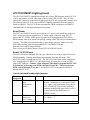
Power Indicator
There is no dedicated power LED indicator on the Data Logger main board. Check 3.3V
at P6 pin 2. The 3.3V power is generated by the LPC315x.
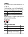
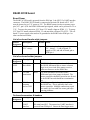
Data Logger boot
The Data Logger boot mode is controlled by the logic level latched at the LPC315x
GPIO0, GPIO1 and GPIO2 pins on the rising edge of RSTIN_N pin. The level of GPIO0
is always low by pull-down R93. The level on GPIO1 is determined by R89 and R92;
GPIO2 is determined by R83 and R92. The level of GPIO1 is indicated by LED D17
(silkscreen MD1). The level of GPIO2 will be indicated by LED D18 (silkscreen MD2).
The LED will be on when GPIOx is high and off when the corresponding GPIOx is low.
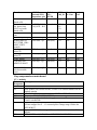
Boot Mode Table
Boot Mode
R83
R92
R89
R94
NAND flash Not installed installed
Not installed installed
SPI
Not installed installed
installed
Not installed
DFU
installed
Not installed Not installed installed
SD/MMC
installed
Not installed installed
Not installed
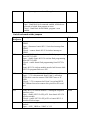
SD/MMC Boot
The SD/MMC power regulator U4 pin 1 must be high to enable the regulator. By default
U4 pin 1 comes up low as it is driven by an external 8-bit register used to provide GPO’s.
Board rework required to boot from SD/MMC
SD/MMC regulator rework for booting from SD/MMC
Lift U4 pin 1 from the pcb to disconnect from U5 pin 5.
Short U4 pin 1 to U4 pin 2.
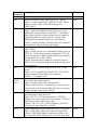
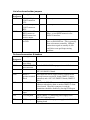
List of on-board header style jumpers
Header
Designator
JP1
JP2
JP3
JP4
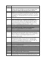
Description
Default
Jennic 802.15.4 wireless module U1 nSPI_MEM_WP
Open – program flash
Closed – SPI Flash write protected
GSM cellular module SERVICE mode select
Open – non-service mode; normal operation
Closed – service mode
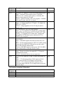
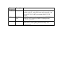
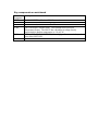
Route external power at J4 through on-board 5V regulator
or bypass regulator.
JP3-2 shunted to JP4-2: 5V external power, bypass
regulator.
JP3-1 shunted to JP3-2; JP4-1 shunted to JP4-2: 6V – 15V
open
open
5V Ext
Power
JP3-2
shunted to
JP4-2