1
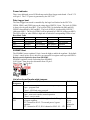
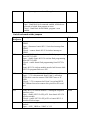
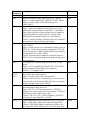
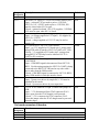
LPC315x Data Logger/Remote Data Acquisition Board
Documentation
Circuit board assembly description
1) Main LPC315x Data Logger board – This is the main Data Logger board.
2) RS232 transceiver board – is used for early s/w development, before Linux is
running on the platform or before the GSM cellular module begins to use the only
UART port on the LPC315x. This board is connected to P15 on the main board
to connect the LPC315x UART to a PC serial port over RS-232.
3) uFL to SMA boards – is used to connect antenna (SMA) to the GSM cellular
module (uFL) plugged in to the main board at J3.
4) LPC1343 VCOM board – is used to provide a SPI to USB virtual comm. Port for
Linux debug. This is needed because there is only one UART port on the
LPC315x chip, and it is used for interfacing to the GSM module. The India team
will need to develop the s/w for LPC1343 SPI-to-USB Vcomm. This board
connects to the main board at P7.
5) RS485 XCVR board – This board contains the RS485 transceiver so the LPC315x
UART port can be used to drive the LPC1102 DMX512 Lighting board using
standard DMX512 cables. The RS485 XCVR board connects to the main DL
board at P15. The GSM cellular module is not useable when the RS485 XCVR
board is attached to main board.
6) LPC31xx Audio board – this board is used with LPC315x internal I2S audio
codec to support stereo headphone out, stereo line level out, stereo line level in,
and Microphone input. This board connects to main board at P8.
7) LPC1102 DMX512 Lighting board – This board is used to demonstrate using the
LPC315x as a DMX512 master lighting controller; while the LPC1102 DMX512
Lighting board is the DMX512 client. The LPC1102 DMX512 board has a 3color LED at D300. This board requires a separate power supply (is not powered
by main DL board). When power is applied to this board all 3 LEDs are on full
brightness. Software to control LPC1102 PWM’s is needed to dim LEDs.
Associated Modules which can be used with the LPC315x Data
Logger/Data Acquisition Board
1) 900/1800 Mhz ¼ wave antenna – used for GSM cellular module. Also requires
uFL-to-SMA board and uFL-to-uFL RF cable to connect antenna to GSM module.
2) WUBR-170GN USB dongle – can add WiFi 802.11 BGN to the Data Logger
when installed at J7 and the appropriate drivers have been installed.
3) JN5148-EK010 Evaluation Kit – contains the Jennic 2.4GHz IEEE802.15.4 &
JenNet development kit. Main DL board has Jennic JN5148 module with onboard antenna for communication with other Jennic JN5148 modules. The intent
is for the Main DL board to be the main controller.
LPC315x Data Logger main board
1B
Board Power
The boards have been shipped to India with jumpers configured for 5V external power
(5V power brick supplied). The DL board is also capable of being powered from an
external dc power source of 6V – 15V (requires different jumper setting at JP3 and JP4).
A 3.6V/3.7V (nominal) Li-Ion battery can be used with either the 5V or 6-15V external
power source.
External power supply Jumper settings
5V external power supply – JP3 pin 2 jumper to JP4 pin 2; caution do not connect to
power supply greater 5.5V in this configuration otherwise there could be damage to
components on the board, including the LPC315x. In this configuration the external 5V
is supplied directly to the board +5V, which supplies the LPC315x PSU_VBUS.
6V – 15V external power supply – JP3 pin 1 to pin 2 jumper; JP4 pin 1 to pin 2 jumper.
In this configuration the external 6-15V is supplied to a step-down power converter
which outputs to the board +5V net.
Using external power only, no Li-Ion battery
When the Data Logger is powered strictly from power mains through the external dc
power jack (J4) and no Li-Ion battery will be connected to the board, diode D6 must be
installed to get power to the GSM cellular module.
Using Li-Ion Battery power
When a Li-Ion battery will be used with the Data Logger board (P2 or P2A), ensure that
D6 is either not installed or lift D6 pin 1 off the pcb.
Battery charger software
The LPC315x battery charger software needs to be developed; India team?
Power Indicator
There is no dedicated power LED indicator on the Data Logger main board. Check 3.3V
at P6 pin 2. The 3.3V power is generated by the LPC315x.
Data Logger boot
The Data Logger boot mode is controlled by the logic level latched at the LPC315x
GPIO0, GPIO1 and GPIO2 pins on the rising edge of RSTIN_N pin. The level of GPIO0
is always low by pull-down R93. The level on GPIO1 is determined by R89 and R92;
GPIO2 is determined by R83 and R92. The level of GPIO1 is indicated by LED D17
(silkscreen MD1). The level of GPIO2 will be indicated by LED D18 (silkscreen MD2).
The LED will be on when GPIOx is high and off when the corresponding GPIOx is low.
Boot Mode Table
Boot Mode
R83
R92
R89
R94
NAND flash Not installed installed
Not installed installed
SPI
Not installed installed
installed
Not installed
DFU
installed
Not installed Not installed installed
SD/MMC
installed
Not installed installed
Not installed
SD/MMC Boot
The SD/MMC power regulator U4 pin 1 must be high to enable the regulator. By default
U4 pin 1 comes up low as it is driven by an external 8-bit register used to provide GPO’s.
Board rework required to boot from SD/MMC
SD/MMC regulator rework for booting from SD/MMC
Lift U4 pin 1 from the pcb to disconnect from U5 pin 5.
Short U4 pin 1 to U4 pin 2.
List of on-board header style jumpers
Header
Designator
JP1
JP2
JP3
JP4
Description
Default
Jennic 802.15.4 wireless module U1 nSPI_MEM_WP
Open – program flash
Closed – SPI Flash write protected
GSM cellular module SERVICE mode select
Open – non-service mode; normal operation
Closed – service mode
Route external power at J4 through on-board 5V regulator
or bypass regulator.
JP3-2 shunted to JP4-2: 5V external power, bypass
regulator.
JP3-1 shunted to JP3-2; JP4-1 shunted to JP4-2: 6V – 15V
open
open
5V Ext
Power
JP3-2
shunted to
JP4-2
external power goes to on-board 5v regulator
JP5
Nand flash Lock select
Open – Nand block lock command enabled, all blocks are
protected or locked from program or erase.
Closed – Nand block lock disabled; program / erase
enabled.
closed
List of on-board solder jumpers
20B
Jumper
Description
Designator
JS1
Jennic 802.15.4 wireless module U1 interrupt to LPC315x
GPIO2
Open – disconnect Jennic 802.15.4 wireless interrupt from
GPIO2
Closed - connect Jennic 802.15.4 wireless interrupt to
GPIO2
JS2
Jennic 802.15.4 wireless module enable flash programming
from LPC315x SPI
Open – disable Jennic 802.15.4 wireless flash programming
from LPC315x SPI
Closed – enable Jennic flash programming from LPC315x
SPI;
Jennic 802.15.4 wireless module must be held in reset while
LPC315x programs flash over SPI
Default
JS3
3.3V connection at GSM Cellular UART trace port P4
Open – 3.3V is disconnected from P4 pin 2; used when
FTDI cable is used to connect GSM UART trace to PC
USB.
Closed – 3.3V is connected to P4 pin 2; use when RS232
XCVR board is used to connect trace port P4 to PC serial
port.
open
JS4
Jennic 802.15.4 wireless module U1 Intelligent Peripheral
interface select
Open – disable LPC315x SPI_nCS1 from Jennic 802.15.4
wireless module.
Closed – enable LPC315x SPI_nCS1 to Jennic 802.15.4
wireless IP select input.
D6 installed +PSU_VBUS to +VBAT voltage for GSM
module
Open – +PSU_VBUS to +VBAT is 3.8V
closed
JS5
closed
open
open
Jumper
Description
Designator
Closed - +PSU_VBUS to +VBAT is 4.2V
JS6
Hardware enable of USB_VBUS_B to +PSU_VBUS
Open – s/w must enable USB_VBUS_B to +PSU_VBUS
Closed – always enable USB_VBUS_B to power
+PSU_VBUS
JS7
Disable 300mA load on external power
Open – 300mA load applied to external power; use only
when board is powered from Li-Ion battery. The 300mA
load is used to ensure external voltage source is capable of
supplying 300mA of current before s/w switches from
battery power to external dc power (i.e. solar panel).
Closed – hardware disable of 300mA load; use for tethered
external power only (no battery) application.
JS8
External power (J4) enabled to power LPC315x
+PSU_VBUS
Open – External power is s/w controlled to supply power to
LPC315x. Used in battery powered application. S/W will
check external power under 300mA load prior to switching
external power on to +PSU_VBUS.
Closed - hardware always enable of external dc power to
LPC315x; use for tethered applications with external power
only (no battery).
JS9
3.3V power to P7 SPI/I2C header for LPC1343 VCOM
board
Open – no 3.3V supplied to P7 header; LPC1343 VCOM
board is powered by the USB Device connector.
Closed – 3.3V supplied to P7
JS10
SPI chip select for LPC1343 VCOM at P7 header; close
JS12
only one of these solder jumpers.
JS13
Open – SPI chip select is not connected to P7
Closed – SPI chip select is connected to P7; close only one
switch and be sure the selected SPI chip select is not being
used for another device on the SPI bus.
JS11
LPC315x 1.8V (+VSUP2) power supplies +VSUP4/8
(external memory bus) power rail
Open – LPC315x 1.8V not used to power +VSUP4/8;
optional 1.8V power supply U23 used to power +VSUP4/8;
JS15 must be closed when JS11 is open.
Closed – LPC315x 1.8V (+VSUP2) supplies +VSUP4/8;
JS15 must be open when JS11 is closed.
JS14
GSM module RING signal connection to LPC315x GPIO1
Open – GSM_RING signal is disconnected from GPIO1
Closed – GSM_RING signal is connected to GPIO1; this
does not affect GPIO1 being used for LPC315x boot mode
Default
open
closed
closed
open
All open
closed
closed
Jumper
Description
Designator
select.
JS15
On-board 1.8V supply to +VSUP4/8 (external memory bus)
Open – on-board 1.8V not used to power +VSUP4/8;
LPC315x 1.8V +VSUP2 used to power +VSUP4/8; JS11
must be closed when JS15 is open.
Closed – optional on-board 1.8V (U23) supplies +VSUP4/8;
JS11 must be open when JS15 is closed.
JS16
On-board optional 1.8V power supply input voltage
Open – no voltage supplied to U23 input; 1.8V supplied by
LPC315x +VSUP2
Closed – voltage supplied to U23; U23 may be used to
supply 1.8V
JS17
3.3V power to P15 LPC315x UART header
Open – no 3.3V supplied to P15 header pin 2; setting when
using FTDI cable to interface LPC315x UART to PC USB.
Closed – 3.3v supplied to P15 header pin 2; setting when
using RS232 XCVR baby board to interface LPC315x
UART to PC serial port.
JS18
GSM module C104/RXD signal connection to LPC315x
UART RXD.
Open – GSM RXD signal is disconnected from LPC315x
RXD. Use this setting anytime the LPC315x UART is being
connected to the RS232 XCVR board or any other cable /
device other than the GSM module.
Closed – GSM RXD signal is connected to LPC315x RXD;
when GSM module is used this must be closed...
JS19
Board system reset source select
Open – System reset driven by simple RC; C122 must be
installed for this mode.
Closed – System reset driven by reset supervisor.
JS20
3.3V to JTAG connector P14 pin 2; bottom side jumper on
PCB.
Open – 3.3V disconnected from JTAG connector P14-2.
Leave open when the JTAG dongle is self-powered.
Closed – 3.3V is connected to JTAG connector P14-2.
Close this jumper when the JTAG dongle must be powered
from the target.
On board connectors & headers
21B
Reference
Designator
J1
J2
J3
Function
Ethernet interface
SD/MMC slot
GSM Cellular module connector; Telit GC864-QUAD_V2
Default
open
open
closed
closed
closed
open
Reference Function
Designator
J4
External DC power; 5V power brick; 6V – 15Vdc
Caution: ensure JP3 and JP4 are set correctly for external voltage
used otherwise damage could result to the board or LPC315x.
J5
Embedded Artists QVGA LCD panel SPI interface for touch screen
J6
USB Device interface connector. The LPC315x can only support one
USB Device or one USB Host but not both at the same time. The USB
Device and Host connectors are multiplexed to the LPC315x. The mux is
controlled by s/w. The default after power on is the Device connected to
the LPC315x.
J7
USB Host interface connector. This connector is multiplexed with J6 for
connection to the LPC315x. See J6 function for additional details.
J8
ANA2_1 analog sensor input, 3-position screw terminal block. The
LPC315x has 3 ADC channels. ADC10B_GPA1 and ADC10B_GPA2
are both connected to an external 4:1 multiplexer chip U15. Which
channel of the multiplexer is connected to the LPC315x ADC is set by
GPO at U5. Analog inputs must be between 0V – 3.3Vdc.
J9
ANA2_0 analog sensor input, 3-position screw terminal block.
J10
ANA1_1 analog sensor input, 3-position screw terminal block.
J11
ANA1_0 analog sensor input, 3-position screw terminal block.
P1
Jennic 802.15.4 wireless module (U1) JTAG connector
P2
Li-Ion battery JST 3-pin connector; this is optional connector for battery.
P2A
Li-Ion battery JST 2-pin connector.
P3
Jennic 802.15.4 wireless module serial interface connector. Used for
programming the flash on the module. May be connected to either the
RS232 XCVR board or FTDI cable to interface to a PC. Programming the
module is required to use the Intelligent Peripheral interface for
interfacing to LPC315x SPI.
P4
GSM cellular module monitor serial interface connector. Used for
reprogramming the module. May be connected to either the RS232
XCVR board or FTDI cable to interface to a PC. The GSM module
responds to AT commands on serial interface to LPC315x UART. No
reprogramming of the GSM module should be needed.
P5
Embedded Artists QVGA LCD panel LCD data interface.
P6
LPC315x I2C expansion interface; may be used for sensors with I2C.
P7
LPC1343 VCOM interface (SPI)
P8
LPC315x Audio Codec analog interface to LPC31xx Audio board.
P9
LPC315x SPI expansion interface; may be used for sensors with SPI.
P10
ANA2_3 analog sensor input, 3-position header.
P11
ANA2_2 analog sensor input, 3-position header.
P12
ANA1_3 analog sensor input, 3-position header.
P13
ANA1_2 analog sensor input, 3-position header.
P14
LPC315x JTAG interface 20-pin connector
P15
LPC315x UART interface; used to connect RS232 XCVR board for early
development debug. Can not be used when GSM module will be used.
Board GPIO function
The GPIO used on the Data logger board are described in the following table. More
GPIO was required than available from the LPC315x alone, so an external 8-bit D-type
flip-flop U5 is used for additional GPO’s. GPIO table column descriptions:
Column 1 – Function; brief name describing what the GPIO is used for.
Column 2 – defines which LPC315x pin name and pin number, or expansion GPO used.
Column 3 – defines how the LPC315x GPIO or expansion GPO comes up after power on
/ reset.
Column 4 – voltage rail the GPIO is powered by. The LPC315x GPIO’s powered by
VDD_IOA (1.8V) use an external buffer U8 to translate to 3.3V.
Column 5 – GPIO function relative to the LPC315x or expansion GPO. The Data logger
start up software must program the LPC315x GPIO according to this column. To
implement an open-drain output OUT (OD), s/w must program GPIO as output to drive
low, but program the same GPIO as input for open-drain state.
Column 6 – active level for GPIO
GPIO function table
Function
LPC315x or
Default
GPIO
Function Active
External GPO
I/O –
Vdd_IO In / Out
level
Expansion - pin PU/PD
SPI-to-USB virtual
mUART_CTS_N In
VDD_I Out
low
comm chip select
/SPI_CS_OUT1 OC –
P11
3.3v
SPI to USB Vcom
I2SRX_WS0 –
During
VDD_I In
low
IRQ
R9
RST high, OC –
then In
3.3v
LCD TS SPI CS
SPI_CS_OUT0 – Out (high) VDD_I Out
low
D8
OC –
3.3v
Jennic chip SPI CS
mUART_CTS_N In
VDD_I Out
low
/SPI_CS_OUT1 OC –
P11 (shared with
3.3v
VCom
Sensor SPI CS
mUART_RTS_N Out (high) VDD_I Out
low
/SPI_CS_OUT2 OC –
R11
3.3v
LCD_BL_INTENS/ PWM_DATA –
In
VDD_I Out
Pwm/h
SHDN
D10
OC –
igh
3.3v
ENET_IRQ
mI2STX_BCK0/ Out (clock) VDD_I In
low
PCM_FSC – T12
OC –
3.3v
DevVBUS-2mNAND_RYBN In
Vdd_IO Out
low
PSU_EN
1/MCI_DAT5 –
A–
C5
1.8V
EXT_PWR 2 PSU
NAND_NCS_1 – Out (high) Vdd_IO Out
low
Ena
L3
A–
Function
LPC315x or
External GPO
Expansion - pin
Default
I/O –
PU/PD
GSM_ON/OFF_PU
LSE
mI2STX_DATA
0/PCM_DA –
T13
mNAND_RYBN
3/MCI_DAT7 –
D4
mNAND_RYBN
2/MCI_DAT6–
D5
GPIO0 – R13
Out (low)
GPIO1 – T14
In / PD
VDD_I
OC –
3.3v
In
GPIO2 – P12
In
VDD_I
OC –
3.3v
In
GPIO3 – D12
In
VDD_I
OC –
3.3v
GPIO4 – D11
In
VDD_I
OC –
3.3v
I2SRX_DATA0 In
VDD_I
– P9
OC –
3.3v
I2SRX_BCK0 – In
VDD_I
T9
OC –
3.3v
NAND_NCS_2 – Out (high) Vdd_IO
L4
A–
1.8V
NAND_NCS_3 – Out (high) Vdd_IO
M2
A–
1.8V
mI2STX_CLK0/ Out (clock) VDD_I
PCM_DB – T11
OC –
In
high
In
low
In
low
In
high
In
Low
(OD)
Out (OD)
Low
(OD)
In
high
EXTPWR_400ma_L
oad_EN
GSM_PWRMON
LPC315x
Boot_Mod0 /
Jennic 802.15.4
wireless module
interrupt
LPC315x
Boot_Mod1 /
GSM module RING
indicator.
LPC315x
Boot_Mod2 /
GSM module DTR
handshake.
PSU_STOP
LCD Touch sceen
Pen_IRQ
SD/MMC nCD
SD/MMC WP
nUSB_Host_Pwr_Fa
ult
LPC315x
nChrg_250mA
Stereo Audio LineIn2 detect from
In
In
In / PD
GPIO
Function
Vdd_IO In / Out
1.8V
VDD_I
OC –
3.3v
Vdd_IO
A–
1.8V
Vdd_IO
A–
1.8V
VDD_I
OC –
3.3v
Active
level
Out
high
(3.3v)
Out
high
In
high
In
Function
LPC31xx Audio
board at P8.
Stereo Audio LineIn1 detect from
LPC31xx Audio
board at P8.
USB_Host Power
ena
SD/MMC_PWR_EN
Analog Mux sel:
EXT_PWR_CHK /
nPSU_VBUS
monitor
Analog port mux
select S0
Analog port mux
select S1
GSM_RESET
USB Mux SEL
nDEVICE/HOST
Jennic 802.15.4
wireless module
reset
LPC315x or
External GPO
Expansion - pin
Default
I/O –
PU/PD
mI2STX_WS0/P
CM_DCK – R12
Out (clock) VDD_I
OC –
3.3v
In
high
GPO EXP – Q0
Out (low)
3.3v
Out
high
GPO EXP – Q1
GPO EXP – Q2
Out (low)
Out (low)
3.3v
3.3v
Out
Out
high
GPO Exp – Q3
Out (low)
3.3v
Out
GPO Exp – Q4
Out (low)
3.3v
Out
GPO Exp – Q5
GPO Exp – Q6
Out (low)
Out (low)
3.3v
3.3v
Out
Out
high
GPO Exp – Q7
Out (low)
3.3v
Out
low
Key components on main board
GPIO
Function
Vdd_IO In / Out
Active
level
3.3v
23B
IC’s / modules
Reference Description
Designator
U2
Ethernet MAC + PHY; Micrel KSZ8851-16MLL.
U1
NXP (Jennic) JN5148-001-M/00T,534 802.15.4 wireless module with onmodule antenna.
U4
SD/MMC 3.3V power regulator; Rohm BD33KA5WFP-E2.
U5
Expansion GPO; NXP 74LVC273PW.
U6
External memory bus 16-bit dual supply transceiver; TI
74AVCA164245GR
U7
External dc power step-down 1.2A voltage regulator; used only when JP3,
JP4 are strapped for 6v – 15v external power voltage range. Diodes Inc
AP5100WG-7.
U10
Optional EEPROM for storage of Ethernet MAC address; not installed as
default.
U11
SDRAM 32M x 16, 1.8V; Micron MT48H32M16LFBF-75:B
Reference Description
Designator
U12
Nand Flash 4Gbit, 2k page, configured 256M x 16, 1.8V; Micron
MT29F4G16ABCHC:C.
U13
LPC3152 MCU; NXP
U15
Dual 4-chan analog mux/demux; used to multiplex two of the LPC315x
ADC channels to analog sensors. Sensor voltage range must be between
0v – 3.3Vdc. NXP 74LV4052DB
U16
USB high speed multiplexer chip; NXP NX3DV221GM. Allows single
LPC315x USB controller to be used either as Device only or Host only.
Default is for USB Device. S/W must write to USB Mux SEL
nDEVICE/HOST GPO Exp – Q7.
U18
External memory bus 8-bit dual supply transceiver; NXP
74AVC8T245PW
U20
1-of-2 decoder/demultiplexer; NXP 74LVC1G19GW; used to decode the
LPC315x static memory chip select 1 (EBI_nSTCS1) in to two separate
address spaces:
1) Ethernet MAC + Phy 0x20020000 – 0x20027FFF (data) or
0x20030xxx (command).
2) Expansion GPO at 0x20028xxx or 0x30038xxx
U23
Optional 1.8V power regulator for devices on external memory bus;
National Semi LM3670MF-1.8. This regulator is not used as a default.
The LPC315x +VSUP2 supplies 1.8V to external memory bus devices.
U24
USB Host port VBUS power switch; Micrel MIC2005A-1YM5.
U26
Board reset supervisor, 2.63V threshold; Diodes Inc. APX809-26SA.
Y1
25Mhz crystal; used for Ethernet MAC + Phy chip.
Y2
12Mhz crystal; used for LPC315x main oscillator.
Y3
32.768Khz crystal; used for LPC3156 RTC.
Switches
Reference Description
Designator
SW1
Jennic 802.15.4 wireless module manual reset; can be used along with
SW2 to place the module in flash programming mode. Note: expansion
GPO GPO_nRES_ZIG (GPO Exp – Q7) must be driven high before the
Jennic module can be programmed or will respond to any serial
communication.
SW2
Jennic 802.15.4 wireless module SPIMISO_Z; when pressed while SW1 is
pressed then released will place the module in programming mode through
the serial interface.
SW3
When pressed supplies high level to LPC315x PSU_ON. Used to
manually turn on LPC315x power supplies when LPC315x is in STOP
mode.
SW4
Manual Data Logger board system reset.
LED’s
Reference Description
Designator
D17
“MD2” silkscreen; Reflects the state of LPC315x GPIO2; at power-on or
reset will reflect boot mode bit-2. LED is on when GPIO2 is high; LED is
off when GPIO2 is low.
D18
“MD1” silkscreen; Reflects the state of LPC315x GPIO1; at power-on or
reset will reflect boot mode bit-1. LED is on when GPIO1 is high; LED is
off when GPIO1 is low.
D1
SD/MMC power indicator
D2
GSM Cellular module status LED; See Telit documentation:
1) Telit_GC864-QUAD_V2_Hardware_User_Guide_r3.pdf
2) Telit_AT_Commands_Reference_Guide_r9.pdf
LCD
24B
The Data Logger supports the Embedded Artists 3.2 inch QVGA color LCD display (EALCD-002) at P5 and J5.
LPC1343 VCOM board
Board Power
25B
The LPC1343 VCOM board is typically powered from the USB Device VBUS connector
J202. It is also possible to power the board from the LPC1343 UART connector P201.
When the board is powered by P201 the USB Device connector J202 must be
disconnected. P7-1 to P7A-1 must be open in both power configurations. See Table for
LPC1343 VCOM board operation mode for how power jumpers are configured in each
mode.
Board / LPC1343 boot
26B
To boot the LPC1343 in ISP mode for programming the internal flash add a jumper shunt
at JP202. The LPC1343 UART is brought out to P201. The LPC1343 UART port can be
connected to a PC through either the RS232 XCVR baby board to PC serial port, or with
an FTDI cable to PC USB port. See LPC1343 Operation mode table for jumper
connections for each mode and power source.
LPC1343 VCOM board operation mode table
Operational
Power
JP201 JP202 Notes
Mode
Source
LPC1343 ISP
J202
2-3
closed RS232 XCVR board installed at P201
mode;
VBUS
3.3V
to program LPC1343 Flash from PC
Use RS232
serial port. The RS232 XCVR board
XCVR brd
is powered from JP201.
LPC1343 ISP
P201
1-2
closed FTDI cable installed at P201 to
mode;
FTDI
5V
program LPC1343 Flash from PC
Use FTDI cable
cable
virtual comm port. No USB Device
installed at J202.
LPCxxxx UART J202
2-3
open
RS232 XCVR board installed at P201
to USB VCP
VBUS
3.3V
to interface with any LPCxxxx MCU
UART port. RS232 XCVR board is
powered from JP201.
LPCxxxx SPI /
J202
open
open
P7A used to interface to SPI or I2C
I2C to USB VCP VBUS
interface of any LPCxxxx MCU. For
Data logger SPI-to-VCP debug port
jumper P7A pins 2, 3, 4, 5, 6, 9, and
10 to the same pins on main board P7.
List of on-board header style jumpers
27B
Header
Description
Designator
P7A
SPI / I2C interface
to LPC315x on
main Data logger
brd
Default Notes
open
For SPI to USB VCOM connect
2,3,4,5,6,9,and 10 to P7 on main brd.
Also select one of three possible SPI chip
selects on the DL main board by adding
Header
Description
Designator
Default Notes
JP201
Power select for
P201
open
JP202
LPC1343 ISP
mode
open
solder to JS10, JS12 or JS13. When no
LCD is used on Data Logger solder JS10.
When RS232 XCVR board is installed at
P201, jumper JP201_2-3 for 3.3V to
XCVR board.
When FTDI cable is installed a P201,
jumper JP201_1_2 for 5V to power
LPC1343 VCOM board from FTDI cable.
USB Device must not be installed at J202.
Short before power-on or reset to bring up
LPC1343 in ISP mode to program internal
Flash.
On board connectors & headers
28B
Reference Description
Designator
P201
LPC1343 UART
interface
J202
USB Device conn
P202
LPC1343 SWD
debug connector
Notes
Connect either RS232 XCVR baby brd or FTDI
cable to program LPC1343 Flash in ISP mode. See
LPC1343 VCOM board operation mode table for
VCOM board jumper settings.
Board typically powered by this connector. USB
device must be disconnected when the board is
powered by the FTDI cable at P201.
RS485 XCVR board
Board Power
The RS485 XCVR board is powered from the P200 pin 3; the LPC315x UART interface
connector. The RS485 XCVR board is connected to the main DL board at P15. SJ17
must be shorted to get 3.3V power to P15. The RS485 transceiver has a separate power
pin (VCC, pin 14) for the RS485 differential pair signals, which can be powered at 5V or
3.3V. To power the transceiver VCC from 3.3V install a shunt at JP200_1-2. To power
VCC from 5V install a shunt at JP200_2-3 and attach the off-board 5V to TP1. The offboard 5V power supply also needs to be grounded to the RS485 brd at P200 pin 1 or
other convenient location.
List of on-board header style jumpers
Header
Description
Designator
JP200
RS485 transceiver
VCC voltage
Default Notes
Open
3.3V – shunt 1 - 2
5V – shunt 2 – 3, add off-board 5V
supply at TP1, and add off board gnd to
P200 pin 1.
List of on-board solder jumpers
Jumper
Description
Designator
JS200
Pull-apart
JS201
bias enable
Default Notes
JS202
120 ohm
termination
Short
JS203
RS485
common
tied to GND
Short
short
DMX512 defines a simple resistor divider to bias
the RS458 differential pair to ensure a known
logic level is received at the master receiver
when no clients are on the RS485 bus.
120 ohm termination across the RS485
differential pair when jumper is shorted. The
master controller should be located at one far end
to the RS485 bus and should have termination
on.
RS485 is generally tied to gnd at one place on
the RS485 bus. This is generally done at the
master controller. Multiple connections to gnd
are usually ok, but could also create gnd loops
causing problems.
On board connectors & headers
Reference Description
Designator
P200
LPC315x
UART
interface
Notes
P200 is connected to the LPC315x UART interface on the
DL main board P15. The transceiver UART interface is
powered from P200 pin 2. Ensure the Data logger main
Reference Description
Designator
J200
DMX512
Out
J201
RS-485 bus
Notes
board has JS17 shorted to get 3.3V to P15. The GSM
module on the DL main board must not be powered on to
use the LPC315x UART port with the RS485 XCVR
board.
XLR-5F connector used to connect standard DMX512
clients to the DL running a DMX512 lighting master
controller application.
3-position screw terminal may also be used to wire up the
RS485 bus to client lighting boards for simple wire
demonstration.
LPC31xx Audio board
Board Power
The LPC31xx Audio board is powered from the P300 pin 9; the LPC315x audio interface
connector. The LPC31xx Audio board is connected to the main DL board at P8.
External power supply Jumper settings:
There are no power supply jumpers for the LPC31xx audio board.
List of on-board header style jumpers:
There are no header style or solder style jumpers on the LPC31xx audio board.
On board connectors & headers
Reference
Designator
P300
J302
J303
J304
J305
Description
Notes
LPC315x analog audio signals, 3.3V power, gnd
Microphone mono input;
Stereo audio line level input1; signal VIN_DETECT high indicates
a cable has been plugged in to J303.
Stereo audio line level input2; signal TIN_DETECT high indicates
a cable has been plugged in to J304.
Stereo headphone output; supports 16 – 32 ohm load.
S232 XCVR board
Board power
The RS232 XCVR board is powered from the P15A pin 3; the uart interface connector.
The RS232 XCVR board is connected to the main DL board at P15.
External power supply Jumper settings:
Solder jumper JS17 must be shorted on the main DL board to supply 3.3v power to P15
pin 3.
List of on-board header style jumpers:
There are no header style or solder style jumpers on the RS232 XCVR board.
On board connectors & headers
Reference Description
Designator
P15A
LPC315x UART interface
P304
DB9 male connector wired as DTE; requires null-modem cable
when connecting to a PC serial port.
Notes
LPC1102 DMX512 lighting board
The LPC1102 DMX512 lighting board makes use of three PWM outputs of the LPC1102
to drive the intensity of each color input of the tri-color LED at D300. The LPC1102
analog ADC inputs are connected to a light sensor (Q303) and a temperature sensor U304.
The concept is the LPC1102 receives DMX512 lighting commands from the main DL
board over RS485. The LPC1102 then programs the PWM according to the DMX512
commands and / or the light and temperature sensors.
Board Power
The LPC1102 DMX512 board is powered from a 5V power brick attached to connector
J306. Power may also be supplied by a 5V bench supply connected using TP2 (5V
power) and TP3 (GND). When power is applied to an unprogrammed LPC1102 the
PWM outputs come up as inputs with pull-up, causing each LED to be lit with maximum
intensity. The LED at maximum intensity is quite bright; you may want to cover the
LED while working with an unprogrammed LPC1102 DMX512 board.
External power supply Jumper settings:
There are no power supply jumpers on the LPC1102 DMX512 board.
Board / LPC1102 boot
The LPC1102 has no dedicated ISP entry pin. Therefore, user code is required to invoke
ISP functionality. Unprogrammed parts automatically boot into ISP mode. The
LPC1102 UART is brought out to P302. The LPC1102 UART port can be connected to
a PC through either the RS232 XCVR baby board to PC serial port, or with an FTDI
cable to PC USB port. Caution - when using an FTDI cable to program the LPC1102
it is necessary to disconnect the FTDI cable pin 3 from P302. This is because the
FTDI cable will output 5V on pin 3. See the LPC1102 User manual for details of
booting the LPC1102.
List of on-board header style jumpers
39B
Header
Description
Designator
JP300
RS-485 120
ohm
terminations
enable.
Default Notes
JP301
Open
RS485
transceiver
VCC voltage
open
Open – termination is disabled.
Shorted – termination is on across the RS485
+ to – signal. Add termination when only the
LPC1102 DMX512 board is the last board
connected in the RS485 daisy chain, or if it’s
the only board on the RS485 bus to a
DMX512 master.
3.3V – shunt 1 - 2
5V – shunt 2 – 3
List of on-board solder jumpers
Jumper
Description
Designator
JS300
LPC1102 P0_9 to
UART connector
CTS
JS301
LPC1102 P0_8 to
UART connector
RTS
JS302
LPC1102 UART
RXD connect to
RS458 transceiver
receive output.
JS303
RS485 common tied
to GND
Default Notes
open
Leave open
Open
Leave open
short
Open – when using LPC1102 ISP.
Short – to use RS485 transceiver for
DMX512 interface.
Short
RS485 is generally tied to gnd at one
place on the RS485 bus. This is generally
done at the master controller. Multiple
connections to gnd are usually ok, but
could also create gnd loops causing
problems.
On board connectors & headers
Reference Description
Notes
Designator
P301
LPC1102 serial
wire debug
P302
LPC1102 UART Used for LPC1102 ISP to program internal flash.
port connector
P303
DMX512 In
5-pin male XLR connector DMX512 input to the
LPC1102 DMX512 board.
J300
RS485 3This connector can be used to connect a small RS485
position terminal network between a main DL board (DMX512 master
block.
controller) and a LPC1102 DMX512 board (DMX512
slave).
J301
DMX512 Out
5-pin female XLR-5F connector used as the output
connector when daisy chain to another DMX512 client
(slave) board. When this connector is used the
termination should be disabled by leaving JP300 open.
J306
5V dc power
input.
TP2
+5V test point
Use to connect +5V bench top power supply to the
LPC1102 Lighting board.
TP3
GND test point
Use to connect bench top power supply to the LPC1102
Lighting board
Key components on main board
Reference
Designator
U300
U302
U303
U304
D300
SW300
Description
MAX13432EETD+, Maxim. RS485 transceiver
SA57000-33D , NXP. 3.3v voltage regulator.
LPC1102 MCU; NXP
LM335M/NOPB, National Semi. Two-terminal zener Precision
Temperature Sensor. The LM135 has a breakdown voltage directly
proportional to absolute temperature at +10 mV/°K.
CLV6A-FKB-CK1P1G1BB7R3R3; Cree. high performance tricolor (red,
green, blue) SMT LED.
LPC1102 MCU reset