1
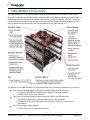
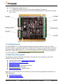
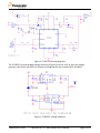
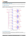
TWR-ADCDAC-LTC Tower Module
User's Manual
Rev. 0
Freescale Semiconductor Inc
TWRADCDACLTCUM
Table of Contents
1 TWR-ADCDAC-LTC Overview ..............................................................................................................4
1.1 Getting Started ..................................................................................................................................................................... 5
1.2 Reference Documents ....................................................................................................................................................... 5
2 Hardware Description ...........................................................................................................................6
2.1 Linear Technology Devices ............................................................................................................................................. 6
2.1.1 LTC2600 ................................................................................................................................................................................................. 6
2.1.2 LTC2704 ................................................................................................................................................................................................. 6
2.1.3 LTC2498 ................................................................................................................................................................................................. 7
2.1.4 LTC1859 ................................................................................................................................................................................................. 7
2.1.5 LTC3471 ................................................................................................................................................................................................. 7
2.1.6 LTC6655 ................................................................................................................................................................................................. 8
2.2 SPI Interface .......................................................................................................................................................................... 8
2.3 System Power .................................................................................................................................................................... 10
2.4 Input/Output Connectors............................................................................................................................................. 12
2.4.1 QuikEval Connectors ..................................................................................................................................................................... 12
2.4.2 ADC and DAC Connections .......................................................................................................................................................... 12
2.4.3 Digital Debug Connector .............................................................................................................................................................. 13
2.5 Jumper Table ..................................................................................................................................................................... 14
2.6 Tower Elevator Connections....................................................................................................................................... 15
TWRADCDACLTCUM
TWR-ADCDAC-LTC Tower Module User's Manual
Page 2 of 17
List of Figures
Figure 1. Freescale Tower System Overview .............................................................................................. 4
The features of the TWR-ADCDAC-LTC peripheral module are listed here and pointed out in Figure 2:.. 4
Figure 2. Callouts on top side of the TWR-ADCDAC-LTC ............................................................................ 5
Figure 3. SPI Configuration Options ............................................................................................................ 9
Figure 4. Power Inputs .............................................................................................................................. 10
Figure 5. LTC3471 Switching Regulator .................................................................................................... 11
Figure 6. LTC6655-5 Voltage Reference.................................................................................................... 11
Figure 7. QuikEval Connectors .................................................................................................................. 12
Figure 8. TWR-ADCDAC-LTC Default Jumper Settings .............................................................................. 15
List of Tables
Table 1. SPI Chip-Select Decoder Truth Table............................................................................................. 9
Table 2. Decoded SPI Chip-Select Device Connections............................................................................. 10
Table 3. Terminal Block Connections ........................................................................................................ 13
Table 4. Digital Debug Connector ............................................................................................................. 14
Table 5. TWR-ADCDAC-LTC Jumper Table ................................................................................................ 14
Table 6. TWR-ADCDAC-LTC Primary Connector Pinout ............................................................................ 15
Revision History
Revision
1.0
TWRADCDACLTCUM
Date
Jan 17, 2010
Changes
Initial Release
TWR-ADCDAC-LTC Tower Module User's Manual
Page 3 of 17
1 TWR-ADCDAC-LTC Overview
The TWR-ADCDAC-LTC is a Tower Peripheral Module compatible with the Freescale Tower System
(Figure 1). It features two analog-to-digital converters (ADC), two digital-to-analog converters (DAC), a
voltage regulator and high-precision voltage reference from Linear Technology. SPI and I2C interface
signal connections on the Primary Elevator Connector allow any Tower Controller Module with a SPI
and I2C interface to configure and control all the features of the TWR-ADCDAC-LTC.
Figure 1. Freescale Tower System Overview
The features of the TWR-ADCDAC-LTC peripheral module are listed here and pointed out in Figure 2:
Two Linear Technology digital-to-analog converters (DACs) with SPI interfaces
o LTC2704-16: Quad 16-bit voltage output SoftSpan™ DAC with readback
o LTC2600: Octal 16-bit rail-to-rail DACs
Two Linear Technology analog-to-digital converters (ADCs) with SPI interfaces
o LTC1859: 8-channel, 16-bit, 100 ksps SoftSpan ADC with shutdown
o LTC2498: 24-bit 8-/16-channel delta sigma ADC with Easy Drive™ input current
cancellation
Linear Technology voltage regulator
o LTC3471: Dual 1.3A, 1.2 MHz boost/inverter
TWRADCDACLTCUM
TWR-ADCDAC-LTC Tower Module User's Manual
Page 4 of 17
Linear Technology voltage reference
o LTC6655-5: 0.25 ppm noise, low drift precision buffered 5V reference
Four 14-pin headers for connecting to any Linear Technology QuikEval™ demonstration board
via I2C or SPI
Figure 2. Callouts on top side of the TWR-ADCDAC-LTC
1.1 Getting Started
The TWR-ADCDAC-LTC is a Tower Peripheral Module that operates under the control of a Tower
Controller Module. A software Demo Suite is available and is the best way to get started and exercise
the features of the TWR-ADCDAC-LTC. A separate lab guide is available to walk the user through the
Demo Suite. Refer to the TWR-ADCDAC-LTC Lab Guide (TWRADCDACLTCLAB) for a list of the Tower
Controller Modules that can run the Demo Suite.
1.2 Reference Documents
The documents and links listed below should be referenced for more information on the TWRADCDAC-LTC and the Tower System.
Freescale Tower System: www.freescale.com/tower
TWR-ADCDAC-LTC Tool Support Page
TWRADCDACLTCQSG: Quick Start Guide
TWRADCDACLTCLAB: Lab Guide and Software
TWRADCDACLTCSCH: Schematics
TWR-ADCDAC-LTC-PWB: Design Package
Please refer to the following links for information on the Linear Technology devices featured on the
TWR-ADCDAC-LTC.
LTC2600 Product Details
LTC2704-16 Product Details
TWRADCDACLTCUM
TWR-ADCDAC-LTC Tower Module User's Manual
Page 5 of 17
LTC2498 Product Details
LTC1859 Product Details
LTC3471 Product Details
LTC6655-5 Product Details
2 Hardware Description
The TWR-ADCDAC-LTC features four Linear Technology converter devices, a voltage regulator and a
high precision voltage reference. Each of the ADCs and DACs on the TWR-ADCDAC-LTC provide a SPI
digital interface for configuration and control. In addition, the QuikEval headers utilize either a SPI or
I2C interface. This section gives an overview of each of the on-board Linear Technology devices and
describes the system power and digital interface configuration options.
2.1 Linear Technology Devices
This section provides a short description of each of the Linear Technology devices on the TWRADCDAC-LTC. Refer to the datasheets and product page links in the “Reference Documents” section
for more product information. Refer to the TWR-ADCDAC-LTC schematics to see how these devices are
connected on the TWR-ADCDAC-LTC.
2.1.1 LTC2600
The LTC2600/LTC2610/LTC2620 are octal 16-, 14- and 12-bit, 2.5V-to-5.5V rail-to-rail voltage-output
DACs in 16-lead narrow SSOP and 20-lead 4mm × 5mm QFN packages. They have built-in high
performance output buffers and are guaranteed monotonic.
These parts establish new board-density benchmarks for 16- and 14-bit DACs and advance
performance standards for output drive, crosstalk and load regulation in single-supply, voltage-output
multiples.
The parts use a simple SPI/MICROWIRE compatible 3-wire serial interface which can be operated at
clock rates up to 50MHz. Daisychain capability and a hardware CLR function are included.
The LTC2600/LTC2610/LTC2620 incorporates a power-on reset circuit. During power-up, the voltage
outputs rise less than 10mV above zero-scale; and after power-up, they stay at zero-scale until a valid
write and update take place.
2.1.2 LTC2704
The LTC2704-16/LTC2704-14/LTC2704-12 are serial input, 12-, 14- or 16-bit, voltage output SoftSpan™
DACs that operate from 3V to 5V logic and ±5V to ±15V analog supplies. SoftSpan offers six output
spans—two unipolar and four bipolar—fully programmable through the 3-wire SPI serial interface. INL
is accurate to 1LSB (2LSB for the LTC2704-16). DNL is accurate to 1LSB for all versions.
Readback commands allow verification of any on-chip register in just one 24- or 32- bit instruction
cycle. All other commands produce a “rolling readback” response from the LTC2704, dramatically
reducing the needed number of instruction cycles.
TWRADCDACLTCUM
TWR-ADCDAC-LTC Tower Module User's Manual
Page 6 of 17
A Sleep command allows any combination of DACs to be powered down. There is also a reset flag and
an offset adjustment pin for each channel.
2.1.3 LTC2498
The LTC2498 is a 16-channel (8-differential) 24-bit No Latency ΔΣ ADC with Easy Drive technology. The
patented sampling scheme eliminates dynamic input current errors and the shortcomings of on-chip
buffering through automatic cancellation of differential input current. This allows large external source
impedances, and rail-to-rail input signals to be directly digitized while maintaining exceptional DC
accuracy.
The LTC2498 includes a high accuracy temperature sensor and an integrated oscillator. This device can
be configured to measure an external signal (from combinations of 16 analog input channels operating
in single ended or differential modes) or its internal temperature sensor. The integrated temperature
sensor offers 1/30th °C resolution and 2°C absolute accuracy.
The LTC2498 allows a wide common mode input range (0V to VCC), independent of the reference
voltage. Any combination of single-ended or differential inputs can be selected and the first conversion
after a new channel is selected is valid. Access to the multiplexer output enables optional external
amplifiers to be shared between all analog inputs and auto calibration continuously removes their
associated offset and drift.
2.1.4 LTC1859
The LTC1857/LTC1858/LTC1859 are 8-channel, low power, 12-/14-/16-bit, 100ksps, analog-to-digital
converters (ADCs). These SoftSpan™ ADCs can be software programmed for 0V to 5V, 0V to 10V, ±5V
or ±10V input spans and operate from a single 5V supply. The 8-channel multiplexer can be
programmed for single-ended inputs or pairs of differential inputs or combinations of both. In addition,
all channels are fault protected to ±25V. A fault condition on any channel will not affect the conversion
result of the selected channel.
An onboard high performance sample-and-hold and precision reference minimize external
components. The low 40mW power dissipation is made even more attractive with two user selectable
power shutdown modes. DC specifications include ±3LSB INL for the LTC1859, ±1.5LSB INL for the
LTC1858 and ±1LSB for the LTC1857.
The internal clock is trimmed for 5µs maximum conversion time and the sampling rate is guaranteed at
100ksps. A separate convert start input and data ready signal (BUSY) ease connections to FIFOs, DSPs
and microprocessors.
2.1.5 LTC3471
The LT3471 dual switching regulator combines two 42V, 1.3A switches with error amplifiers that can
sense to ground providing boost and inverting capability. The low VCESAT bipolar switches enable the
device to deliver high current outputs in a small footprint. The LT3471 switches at 1.2MHz, allowing the
use of tiny, low cost and low profile inductors and capacitors. High inrush current at start-up is
eliminated using the programmable soft-start function, where an external RC sets the current ramp
rate. A constant frequency current mode PWM architecture results in low, predictable output noise
that is easy to filter.
TWRADCDACLTCUM
TWR-ADCDAC-LTC Tower Module User's Manual
Page 7 of 17
The LT3471 switches are rated at 42V, making the device ideal for boost converters up to ±40V as well
as SEPIC and flyback designs. Each channel can generate 5V at up to 630mA from a 3.3V supply, or 5V
at 510mA from four alkaline cells in a SEPIC design. The device can be configured as two boosts, a
boost and inverter or two inverters.
The LT3471 is available in a low profile (0.75mm) 10-lead 3mm × 3mm DFN package.
2.1.6 LTC6655
The LTC6655 is a complete family of precision bandgap voltage references, offering exceptional noise
and drift performance. This low noise and drift is ideally suited for the high resolution measurements
required by instrumentation and test equipment. In addition, the LTC6655 is fully specified over the
temperature range of –40°C to 125°C, ensuring its suitability for demanding automotive and industrial
applications. Advanced curvature compensation allows this bandgap reference to achieve a drift of less
than 2ppm/°C with a predictable temperature characteristic and an output voltage accurate to
±0.025%, reducing or eliminating the need for calibration.
The LTC6655 can be powered from as little as 500mV above the output voltage to as much as 13.2V.
Superior load regulation with source and sink capability, coupled with exceptional line rejection,
ensures consistent performance over a wide range of operating conditions. A shutdown mode is
provided for low power applications. Available in a small MSOP package, the LTC6655 family of
references is an excellent choice for demanding precision applications.
2.2 SPI Interface
There are eight possible SPI devices on the TWR-ADCDAC-LTC: four ADC and DAC devices and four
QuikEval connectors. The Primary Elevator Connector of the Tower System defines two SPI interface
connections, but each only offers up to two chip-selects. Therefore, a 74HC138 3-to-8 line decoder
along with three GPIO signals is used to generate the eight chip-select signals needed to accommodate
all the possible SPI devices on the board. Figure 3 shows the schematic connections for the SPI
configuration selections. Refer to Section 2.4.3 “Jumper Table” for more details on the jumper
selection options.
The three signals decoded by the 74HC138 to generate the SPI chip-select signals can be driven by
GPIO signals from the Primary Elevator Connector (GPIO7-9) or they can be set by jumper options J14J16. Table 1 shows how the logic level on the three decoder inputs map to the SPI chip-select signals.
Table 2 shows the devices to which the decoded chip-selects are connected.
TWRADCDACLTCUM
TWR-ADCDAC-LTC Tower Module User's Manual
Page 8 of 17
Figure 3. SPI Configuration Options
Table 1. SPI Chip-Select Decoder Truth Table
GPIO9 GPIO8 GPIO7
J14
J15
J16
L
L
L
L
H
H
H
H
TWRADCDACLTCUM
L
L
H
H
L
L
H
H
L
H
L
H
L
H
L
H
0
L
H
H
H
H
H
H
H
Decoded SPI Chip-Select
1 2 3 4 5 6
H H H H H H
L H H H H H
H L H H H H
H H L H H H
H H H L H H
H H H H L H
H H H H H L
H H H H H H
7
H
H
H
H
H
H
H
L
TWR-ADCDAC-LTC Tower Module User's Manual
Page 9 of 17
Table 2. Decoded SPI Chip-Select Device Connections
Decoded CS Signal
SPI_CS_DEC0
SPI_CS_DEC1
SPI_CS_DEC2
SPI_CS_DEC3
SPI_CS_DEC4
SPI_CS_DEC5
SPI_CS_DEC6
SPI_CS_DEC7
Device
QuikEval J22
QuikEval J21
QuikEval J20
QuikEval J19
LTC2704
LTC2600
LTC2498
LTC1859
2.3 System Power
The Freescale Tower System supplies 3.3V and 5V supplies on the Elevator Connectors. However, the
TWR-ADCDAC-LTC can—and by default, does—generate its own voltage supply and voltage reference
from the 5V input on a standard mini-B USB connector (J33). As shown in Figure 4, jumper J30 can
optionally be used to provide 5V from the Tower Elevator Connectors.
Figure 4. Power Inputs
The LTC3471 dual switching regulator (Figure 5) boosts and inverts the 5V input to generate clean +15V
and -15V supply rails used by the LTC2704 ADC and the LTC6655-5 voltage regulator.
TWRADCDACLTCUM
TWR-ADCDAC-LTC Tower Module User's Manual
Page 10 of 17
Figure 5. LTC3471 Switching Regulator
The LTC6655-5 precise bandgap voltage reference (Figure 6) uses the +15V as the input voltage
generate a low-noise, low-drift 5.0V reference voltage used by the on-board ADCs and DACs.
Figure 6. LTC6655-5 Voltage Reference
TWRADCDACLTCUM
TWR-ADCDAC-LTC Tower Module User's Manual
Page 11 of 17
2.4 Input/Output Connectors
All the input and output connections on the TWR-ADCDAC-LTC are described in the following sections.
2.4.1 QuikEval Connectors
The QuikEval Connectors utilize either an I2C or SPI interface. Jumpers (J1-J8) are provided to select
between I2C and SPI. These connectors can be used to connect to any Linear Technology evaluation
board that is a member of the QuikEval family.
Figure 7. QuikEval Connectors
2.4.2 ADC and DAC Connections
The inputs and outputs of the four converter devices on the TWR-ADCDAC-LTC are brought to
terminals on screw-in terminal blocks. The following table provides the information for how the signals
are connected to the terminal blocks.
TWRADCDACLTCUM
TWR-ADCDAC-LTC Tower Module User's Manual
Page 12 of 17
Table 3. Terminal Block Connections
LTC Device
LTC2600 DAC
LTC2704 DAC
LTC2498 ADC
LTC1859 ADC
Signal
Connection Label
―
VOUTA
VOUTB
VOUTC
VOUTD
VOUTE
VOUTF
VOUTG
VOUTH
―
―
VOUTA
―
VOUTB
―
VOUTC
―
VOUTD
―
COM
CH0
CH1
CH2
―
―
CH3
CH4
CH5
CH6
CH7
―
COM
CH0
CH1
CH2
CH3
―
CH4
CH5
CH6
CH7
―
J18 pin 1
J18 pin 2
J18 pin 3
J18 pin 4
J18 pin 5
J18 pin 6
J18 pin 7
J18 pin 8
J18 pin 9
J18 pin 10
J17 pin 1
J17 pin 2
J17 pin 3
J17 pin 4
J17 pin 5
J17 pin 6
J17 pin 7
J17 pin 8
J26 pin 1
J26 pin 2
J26 pin 3
J26 pin 4
J26 pin 5
J26 pin 6
J26 pin 7
J26 pin 8
J26 pin 9
J26 pin 10
J26 pin 11
J26 pin 12
J27 pin 1
J27 pin 2
J27 pin 3
J27 pin 4
J27 pin 5
J27 pin 6
J27 pin 7
J27 pin 8
J27 pin 9
J27 pin 10
J27 pin 11
J27 pin 12
GND
A
B
C
D
E
F
G
H
GND
GND
A
GND
B
GND
C
GND
D
GND
COM
0
1
2
GND
GND
3
4
5
6
7
GND
COM
0
1
2
3
GND
4
5
6
7
GND
2.4.3 Digital Debug Connector
A 1x10, 0.1” pitch header with many of the digital communication signals is provided for easy debug
access. Refer to Table 4 to the signal connection details.
TWRADCDACLTCUM
TWR-ADCDAC-LTC Tower Module User's Manual
Page 13 of 17
Table 4. Digital Debug Connector
J38 Pin Number
1
2
3
4
5
6
7
8
9
10
Signal Connection
SPI_CS_DEC4
SPI_CS_DEC5
SPI_CS_DEC6
SPI_CS_DEC7
SPI_CLK
SPI_MOSI
SPI_MISO
SCL0
SDA0
GND
2.5 Jumper Table
There are several jumpers on the TWR-ADCDAC-LTC that provide configuration selection and signal
isolation. Refer to the following table for details. The default installed jumper settings are shown in
bold. The default jumper shunt locations are also shown in Figure 8.
Table 5. TWR-ADCDAC-LTC Jumper Table
Jumper
J1 - J8
Option
QuikEval I2C/SPI Selection
J9
SPI Port Selection -- SPI_CLK
J10
SPI Port Selection -- SPI0_CSx
J11
SPI Port Selection -- SPI1_CSx
J12
SPI Port Selection -- SPI_MOSI
J13
SPI Port Selection -- SPI_MISO
J25
SPI Port Selection -- SPI_CS
J14
SPI Chip-Select Encoding Bit 0 Setting
J15
SPI Chip-Select Encoding Bit 1 Setting
J16
SPI Chip-Select Encoding Bit 2 Setting
J28, J29
J31, J32
J30
LTC2704 VOSx GND Connection
Tower Power Connection
TWRADCDACLTCUM
Setting
1-2
2-3
1-2
2-3
1-2
2-3
1-2
2-3
1-2
2-3
1-2
2-3
1-2
2-3
1-2
2-3
OFF
1-2
2-3
OFF
1-2
2-3
OFF
ON
OFF
ON
OFF
Description
Connect I2C signals to QuikEval header
Connect SPI signals to QuikEval header
Use SPI_CLK signal from SPI0
Use SPI_CLK signal from SPI1
Select SPI0_CS0
Select SPI0_CS1
Select SPI1_CS0
Select SPI1_CS1
Use SPI_MOSI signal from SPI0
Use SPI_MOSI signal from SPI1
Use SPI_MISO signal from SPI0
Use SPI_MISO signal from SPI1
Use SPI0_CSx (see J10)
Use SPI1_CSx (see J11)
Connected to 3.3V
Connected to GND
Driven by GPIO9
Connected to 3.3V
Connected to GND
Driven by GPIO8
Connected to 3.3V
Connected to GND
Driven by GPIO7
Connect VOSA, VOSB, VOSC, VOSD to GND
Disconnect VOSx from GND
Connect on-board 5V rail to Tower System
Isolate on-board 5V rail from Tower System
TWR-ADCDAC-LTC Tower Module User's Manual
Page 14 of 17
Jumper
Option
J34
LT3471 Shutdown
J37
LTC1859 Reference Voltage Selection
Setting
1-2
2-3
ON
OFF
Description
LT3471 voltage regulator enabled
LT3471 voltage regulator disabled
Use output of LTC6655-5 as reference
Use GND as reference
Figure 8. TWR-ADCDAC-LTC Default Jumper Settings
2.6 Tower Elevator Connections
The TWR-ADCDAC-LTC features two expansion card-edge connectors that interface to the Primary and
Secondary Elevator boards in a Tower system. The Primary Connector (comprised of sides A and B) is
utilized by the TWR-ADCDAC-LTC while the Secondary Connector (comprised of sides C and D) only
makes connections to the GND pins. Table 6 provides the pinout for the Primary Connector. An “X” in
the “Used “column indicates that a connection is made to that pin on the connector. An “X” in the
“Jmp” column indicates that a jumper or other option is provided to remove or configure the
connection—thus the connection can be removed if required.
Table 6. TWR-ADCDAC-LTC Primary Connector Pinout
TWR-ADCDAC-LTC Primary Connector
Side B
Pin
#
Name
B1
5V
TWRADCDACLTCUM
Usage
5.0V Power
Used
X
Jmp
Side A
Pin
#
Name
A1
5V
TWR-ADCDAC-LTC Tower Module User's Manual
Usage
5.0V Power
Used
Jmp
X
Page 15 of 17
TWR-ADCDAC-LTC Primary Connector
Side B
Pin
#
Name
B2
GND
Ground
B3
3.3V
3.3V Power
B4
ELE_PS_SENSE
B5
B6
Side A
Pin
#
Name
X
A2
GND
Ground
X
X
A3
3.3V
3.3V Power
X
Power Sense
X
A4
3.3V
3.3V Power
X
GND
Ground
X
A5
GND
Ground
X
GND
SDHC_CLK / SPI1_CLK
Ground
SPI1_CLK
X
X
A6
B7
X
A7
GND
SCL0
Ground
SCL0
X
X
X
B8
SDHC_D3 / SPI1_CS1_b
X
X
A8
SDA0
SDA0
X
X
B9
SDHC_D3 / SPI1_CS0_b
SPI1_CS1
SPI1_CS0
X
X
A9
GPIO9 / CTS1
GPIO9
X
X
B10
SDHC_CMD / SPI1_MOSI
SPI1_MOSI
X
X
A10
GPIO8 / SDHC_D2
GPIO8
X
X
B11
SDHC_D0 / SPI1_MISO
SPI1_MISO
X
X
A11
GPIO7 / SD_WP_DET
GPIO7
X
X
Ground
X
Ground
X
3.3V Power
X
Usage
Used
Jmp
B12
ETH_COL
A12
ETH_CRS
B13
ETH_RXER
A13
ETH_MDC
B14
ETH_TXCLK
A14
ETH_MDIO
B15
ETH_TXEN
A15
ETH_RXCLK
B16
ETH_TXER
A16
ETH_RXDV
B17
ETH_TXD3
A17
ETH_RXD3
B18
ETH_TXD2
A18
ETH_RXD2
B19
ETH_TXD1
A19
ETH_RXD1
B20
ETH_TXD0
A20
ETH_RXD0
B21
GPIO1 / RTS1
A21
SSI_MCLK
B22
GPIO2 / SDHC_D1
A22
SSI_BCLK
B23
GPIO3
A23
SSI_FS
A24
SSI_RXD
A25
SSI_TXD
A26
B24
CLKIN0
B25
CLKOUT1
B26
B27
GND
AN7
A27
GND
AN3
B28
AN6
A28
AN2
B29
AN5
A29
AN1
B30
AN4
A30
AN0
B31
GND
DAC1
A31
B32
A32
GND
DAC0
B33
TMR3
A33
TMR1
B34
TMR2
A34
TMR0
B35
GPIO4
A35
GPIO6
B36
A36
B37
3.3V
PWM7
A37
3.3V
PWM3
B38
PWM6
A38
PWM2
B39
PWM5
A39
PWM1
B40
PWM4
A40
PWM0
B41
CANRX0
A41
RXD0
B42
CANTX0
A42
TXD0
B43
1WIRE
A43
RXD1
B44
SPI0_MISO
SPI0_MISO
X
X
A44
TXD1
B45
SPI0_MOSI
SPI0_MOSI
X
X
A45
VSS
B46
SPI0_CS0_b
SPI0_CS0
X
X
A46
VDDA
B47
SPI0_CS1_b
SPI0_CS1
X
X
A47
VREFA1
TWRADCDACLTCUM
Ground
Ground
3.3V Power
X
X
X
TWR-ADCDAC-LTC Tower Module User's Manual
Usage
Used
Jmp
Page 16 of 17
TWR-ADCDAC-LTC Primary Connector
Pin
#
B48
B49
Side B
Name
SPI0_CLK
Usage
SPI0_CLK
X
Jmp
X
Side A
Pin
#
Name
A48
VREFA2
B50
GND
SCL1
B51
SDA1
A51
GPIO15
B52
GPIO5 / SD_CARD_DET
A52
GPIO16
B53
USB0_DP_PDOWN
A53
B54
A54
GPIO17
USB0_DM
B55
USB0_DM_PDOWN
IRQ_H
A55
USB0_DP
B56
IRQ_G
A56
USB0_ID
B57
IRQ_F
A57
USB0_VBUS
B58
IRQ_E
A58
TMR7
B59
IRQ_D
A59
TMR6
B60
IRQ_C
A60
TMR5
B61
IRQ_B
A61
TMR4
B62
IRQ_A
A62
RSTIN_b
B63
EBI_ALE / EBI_CS1_b
A63
RSTOUT_b
B64
EBI_CS0_b
A64
CLKOUT0
B65
GND
A65
GND
B66
EBI_AD15
A66
EBI_AD14
B67
EBI_AD16
A67
EBI_AD13
B68
EBI_AD17
A68
EBI_AD12
B69
A69
EBI_AD11
B70
EBI_AD18
EBI_AD19
A70
EBI_AD10
B71
EBI_R/W_b
A71
EBI_AD9
B72
EBI_OE_b
A72
EBI_AD8
B73
EBI_D7
A73
EBI_AD7
B74
EBI_D6
A74
EBI_AD6
B75
EBI_D5
A75
EBI_AD5
B76
EBI_D4
A76
EBI_AD4
B77
EBI_D3
A77
EBI_AD3
B78
EBI_D2
A78
EBI_AD2
B79
EBI_D1
A79
EBI_AD1
B80
EBI_D0
A80
EBI_AD0
B81
GND
Ground
X
A81
B82
3.3V
3.3V Power
X
A82
TWRADCDACLTCUM
Ground
Used
X
Ground
X
A49
GND
A50
GPIO14
Usage
Used
Ground
X
GND
Ground
X
3.3V
3.3V Power
X
TWR-ADCDAC-LTC Tower Module User's Manual
Jmp
Page 17 of 17