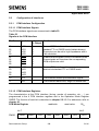
1
ICs for Communications
Extended Line Card Interface Controller
ELIC®
PEB 20550
PEF 20550
Versions 1.3
User’s Manual 01.96
T2055-0V13-M1-7600
Edition 01.96
This edition was realized using the software
system FrameMaker.
Published by Siemens AG,
Bereich Halbleiter, MarketingKommunikation, Balanstraße 73,
81541 München
© Siemens AG 1996.
All Rights Reserved.
Attention please!
As far as patents or other rights of third parties are concerned, liability is only assumed
for components, not for applications, processes and circuits implemented within components or assemblies.
The information describes the type of component and shall not be considered as assured
characteristics.
Terms of delivery and rights to change design
reserved.
For questions on technology, delivery and
prices please contact the Semiconductor
Group Offices in Germany or the Siemens
Companies and Representatives worldwide
(see address list).
Due to technical requirements components
may contain dangerous substances. For information on the types in question please
contact your nearest Siemens Office, Semiconductor Group.
Siemens AG is an approved CECC manufacturer.
Packing
Please use the recycling operators known to
you. We can also help you – get in touch with
your nearest sales office. By agreement we
will take packing material back, if it is sorted.
You must bear the costs of transport.
For packing material that is returned to us unsorted or which we are not obliged to accept,
we shall have to invoice you for any costs incurred.
Components used in life-support devices
or systems must be expressly authorized
for such purpose!
Critical components1 of the Semiconductor
Group of Siemens AG, may only be used in
life-support devices or systems2 with the express written approval of the Semiconductor
Group of Siemens AG.
1 A critical component is a component used
in a life-support device or system whose
failure can reasonably be expected to
cause the failure of that life-support device or system, or to affect its safety or effectiveness of that device or system.
2 Life support devices or systems are intended (a) to be implanted in the human
body, or (b) to support and/or maintain
and sustain human life. If they fail, it is
reasonable to assume that the health of
the user may be endangered.
PEB 20550
PEF 20550
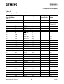
Revision History:
User’s Manual 01.96
Previous Release:
Technical Manual 9.93
Page (in
Previous
Release)
Page
(in User’s
Manual)
Subjects (major changes since last revision)
−
13
PEF 20550 (ext. temperature range; new)
−
38
System Integration and Application (DECT added)
29
46
Boundary scan number 22 = 110 (correction)
29
46
Boundary scan number 9: ID code for V1.3 added
31
49
Boundary scan ID code for V1.3 added
−
57
DMA-transfers, figure 31 (new)
−
60
Support of the HDLC protocol by SACCO, figure 35 (new)
51
76
SACCO clock mode 2 description (extended)
53
80
Extensions for V1.3
55
82
Arbiter state machine description (extended)
58
85
Table 14: Control channel delay examples (extended)
65
95
Internal reference clock RCL replaced by CFI reference clock CRCL
−
101
Interrupt driven transmission sequence example, figure 50 (new)
82
114
Internal reference clock RCL replaced by CFI reference clock CRCL
85
118
Register address arrangement (extended)
−
129
EMOD: ECMD2 restriction 5 (new)
93
130
PMOD: PMD1..0 description (data rate stepping corrected)
101
140
CMD2: CXF, CRR description (corrected)
104
144
MACR description (extended)
114
154
TIMR: SSR (correction)
121
162
VNSR: VN3..0 = V1.2 (correction)
124
167
EXIR: XMR description (extended)
128
172
CCR1: ODS description (extended for V1.3)
132
177
SACCO RSTA: C/R description (new)
140
185
VSTR: VN3..0 value for V1.3 added
142
187
SCV: SCV7...0 description (extended)
−
191
Application Hints (new)
148
380
tALS min = 8 ns, tDRH max = 65 ns, tAH min = 0 ns (correction)
−
395
Package outlines (new)
−
396
Appendix (new)
PEB 20550
Table of Contents
1
1.1
1.2
1.3
1.4
1.5
1.6
1.6.1
1.6.1.1
1.6.1.2
1.6.1.3
Page
1.6.2
1.6.3
1.6.4
1.6.4.1
1.6.4.2
Overview . . . . . . . . . . . . . . . . . . . . . . . . . . . . . . . . . . . . . . . . . . . . . . . . . .11
Features . . . . . . . . . . . . . . . . . . . . . . . . . . . . . . . . . . . . . . . . . . . . . . . . . .13
Pin Configuration (top view) . . . . . . . . . . . . . . . . . . . . . . . . . . . . . . . . . . .15
Pin Definitions and Functions . . . . . . . . . . . . . . . . . . . . . . . . . . . . . . . . . .16
Logic Symbol . . . . . . . . . . . . . . . . . . . . . . . . . . . . . . . . . . . . . . . . . . . . . . .23
Functional Block Diagram . . . . . . . . . . . . . . . . . . . . . . . . . . . . . . . . . . . . .24
System Integration and Application . . . . . . . . . . . . . . . . . . . . . . . . . . . . . .25
Digital Line Card . . . . . . . . . . . . . . . . . . . . . . . . . . . . . . . . . . . . . . . . . . . .25
Switching, Layer-1 Control, Group Controller Signaling . . . . . . . . . . . . . .25
Decentralized D-Channel Processing, Multiplexed HDLC-Controller. . . . .27
Decentralized D-Channel Processing,
Dedicated HDLC-Controller per Subscriber . . . . . . . . . . . . . . . . . . . . . . .31
Decentralized D-Channel Processing, Multiplexed plus
Dedicated HDLC-Control . . . . . . . . . . . . . . . . . . . . . . . . . . . . . . . . . . . . . .31
Central D-Channel Processing . . . . . . . . . . . . . . . . . . . . . . . . . . . . . . . . .33
Mixed D-Channel Processing, Signaling Decentralized,
Packet Data Centralized . . . . . . . . . . . . . . . . . . . . . . . . . . . . . . . . . . . . . .34
Key Systems . . . . . . . . . . . . . . . . . . . . . . . . . . . . . . . . . . . . . . . . . . . . . . .36
Analog Line Card . . . . . . . . . . . . . . . . . . . . . . . . . . . . . . . . . . . . . . . . . . . .37
DECT Applications . . . . . . . . . . . . . . . . . . . . . . . . . . . . . . . . . . . . . . . . . .38
Adaptation of a DECT System to an Existing PBX . . . . . . . . . . . . . . . . . .38
DECT Line Card Design for an Existing PBX . . . . . . . . . . . . . . . . . . . . . .40
2
2.1
2.2
2.2.1
2.2.2
2.2.3
2.2.4
2.2.5
2.2.5.1
2.2.5.2
2.2.6
2.2.6.1
2.2.6.2
2.2.6.3
2.2.6.4
2.2.6.5
2.2.7
2.2.7.1
2.2.7.2
2.2.7.3
Functional Description. . . . . . . . . . . . . . . . . . . . . . . . . . . . . . . . . . . . . . .41
General Functions and Device Architecture . . . . . . . . . . . . . . . . . . . . . . .41
Functional Blocks . . . . . . . . . . . . . . . . . . . . . . . . . . . . . . . . . . . . . . . . . . .41
Bus Interface . . . . . . . . . . . . . . . . . . . . . . . . . . . . . . . . . . . . . . . . . . . . . . .41
Parallel Ports . . . . . . . . . . . . . . . . . . . . . . . . . . . . . . . . . . . . . . . . . . . . . . .42
Watchdog Timer . . . . . . . . . . . . . . . . . . . . . . . . . . . . . . . . . . . . . . . . . . . .43
Reset Logic . . . . . . . . . . . . . . . . . . . . . . . . . . . . . . . . . . . . . . . . . . . . . . . .43
Boundary Scan Support . . . . . . . . . . . . . . . . . . . . . . . . . . . . . . . . . . . . . .45
Boundary Scan . . . . . . . . . . . . . . . . . . . . . . . . . . . . . . . . . . . . . . . . . . . . .45
TAP-Controller . . . . . . . . . . . . . . . . . . . . . . . . . . . . . . . . . . . . . . . . . . . . . .48
EPIC®-1 . . . . . . . . . . . . . . . . . . . . . . . . . . . . . . . . . . . . . . . . . . . . . . . . . .49
PCM-Interface . . . . . . . . . . . . . . . . . . . . . . . . . . . . . . . . . . . . . . . . . . . . . .49
Configurable Interface . . . . . . . . . . . . . . . . . . . . . . . . . . . . . . . . . . . . . . . .50
Memory Structure and Switching . . . . . . . . . . . . . . . . . . . . . . . . . . . . . . . .50
Pre-processed Channels, Layer-1 Support . . . . . . . . . . . . . . . . . . . . . . . .51
Special Functions . . . . . . . . . . . . . . . . . . . . . . . . . . . . . . . . . . . . . . . . . . .52
SACCO . . . . . . . . . . . . . . . . . . . . . . . . . . . . . . . . . . . . . . . . . . . . . . . . . . .52
Block Diagram . . . . . . . . . . . . . . . . . . . . . . . . . . . . . . . . . . . . . . . . . . . . . .52
Parallel Interface . . . . . . . . . . . . . . . . . . . . . . . . . . . . . . . . . . . . . . . . . . . .53
FIFO-Structure . . . . . . . . . . . . . . . . . . . . . . . . . . . . . . . . . . . . . . . . . . . . . .57
1.6.1.4
1.6.1.5
1.6.1.6
Semiconductor Group
4
01.96
PEB 20550
Table of Contents
Page
2.2.7.4
2.2.7.5
2.2.7.6
2.2.7.7
2.2.7.8
2.2.8
2.2.8.1
2.2.8.2
2.2.8.3
2.2.8.4
Protocol Support . . . . . . . . . . . . . . . . . . . . . . . . . . . . . . . . . . . . . . . . . . . .60
Special Functions . . . . . . . . . . . . . . . . . . . . . . . . . . . . . . . . . . . . . . . . . . .75
Serial Interface . . . . . . . . . . . . . . . . . . . . . . . . . . . . . . . . . . . . . . . . . . . . .76
Serial Port Configuration . . . . . . . . . . . . . . . . . . . . . . . . . . . . . . . . . . . . . .79
Test Mode . . . . . . . . . . . . . . . . . . . . . . . . . . . . . . . . . . . . . . . . . . . . . . . . .80
D-Channel Arbiter . . . . . . . . . . . . . . . . . . . . . . . . . . . . . . . . . . . . . . . . . . .81
Upstream Direction . . . . . . . . . . . . . . . . . . . . . . . . . . . . . . . . . . . . . . . . . .82
Downstream Direction . . . . . . . . . . . . . . . . . . . . . . . . . . . . . . . . . . . . . . . .86
Control Channel Delay . . . . . . . . . . . . . . . . . . . . . . . . . . . . . . . . . . . . . . .87
D-Channel Arbiter Co-operating with QUAT-S Circuits . . . . . . . . . . . . . . .88
3
3.1
3.2
3.3
3.4
3.5
3.5.1
3.5.2
3.5.3
3.5.4
3.6
3.6.1
3.6.2
3.6.3
3.6.4
3.7
3.7.1
3.7.2
3.8
3.8.1
3.8.2
3.8.2.1
3.8.2.2
3.8.2.3
3.8.2.4
3.8.3
3.8.4
3.8.5
3.8.6
3.8.6.1
3.8.6.2
3.8.6.3
Operational Description . . . . . . . . . . . . . . . . . . . . . . . . . . . . . . . . . . . . . .89
Microprocessor Interface Operation . . . . . . . . . . . . . . . . . . . . . . . . . . . . .89
Interrupt Structure and Logic . . . . . . . . . . . . . . . . . . . . . . . . . . . . . . . . . . .90
Clocking . . . . . . . . . . . . . . . . . . . . . . . . . . . . . . . . . . . . . . . . . . . . . . . . . . .91
Reset . . . . . . . . . . . . . . . . . . . . . . . . . . . . . . . . . . . . . . . . . . . . . . . . . . . . .92
EPIC®-1 Operation . . . . . . . . . . . . . . . . . . . . . . . . . . . . . . . . . . . . . . . . . .92
PCM-Interface . . . . . . . . . . . . . . . . . . . . . . . . . . . . . . . . . . . . . . . . . . . . . .93
Configurable Interface . . . . . . . . . . . . . . . . . . . . . . . . . . . . . . . . . . . . . . . .94
Switching Functions . . . . . . . . . . . . . . . . . . . . . . . . . . . . . . . . . . . . . . . . . .95
Special Functions . . . . . . . . . . . . . . . . . . . . . . . . . . . . . . . . . . . . . . . . . . .99
SACCO-A/B . . . . . . . . . . . . . . . . . . . . . . . . . . . . . . . . . . . . . . . . . . . . . . . .99
Data Transmission in Interrupt Mode . . . . . . . . . . . . . . . . . . . . . . . . . . . .99
Data Transmission in DMA-Mode . . . . . . . . . . . . . . . . . . . . . . . . . . . . . .101
Data Reception in Interrupt Mode . . . . . . . . . . . . . . . . . . . . . . . . . . . . . .102
Data Reception in DMA-Mode . . . . . . . . . . . . . . . . . . . . . . . . . . . . . . . . .103
D-Channel Arbiter . . . . . . . . . . . . . . . . . . . . . . . . . . . . . . . . . . . . . . . . . .104
SACCO-A Transmission . . . . . . . . . . . . . . . . . . . . . . . . . . . . . . . . . . . . .104
SACCO-A Reception . . . . . . . . . . . . . . . . . . . . . . . . . . . . . . . . . . . . . . . .105
Initialization Procedure . . . . . . . . . . . . . . . . . . . . . . . . . . . . . . . . . . . . . .106
Hardware Reset . . . . . . . . . . . . . . . . . . . . . . . . . . . . . . . . . . . . . . . . . . . .106
EPIC®-1 Initialization . . . . . . . . . . . . . . . . . . . . . . . . . . . . . . . . . . . . . . . .106
Register Initialization . . . . . . . . . . . . . . . . . . . . . . . . . . . . . . . . . . . . . . . .106
Control Memory Reset . . . . . . . . . . . . . . . . . . . . . . . . . . . . . . . . . . . . . . .106
Initialization of Pre-processed Channels . . . . . . . . . . . . . . . . . . . . . . . . .107
Initialization of the Upstream Data Memory (DM) Tristate Field . . . . . . .109
SACCO-Initialization . . . . . . . . . . . . . . . . . . . . . . . . . . . . . . . . . . . . . . . .109
Initialization of D-Channel Arbiter . . . . . . . . . . . . . . . . . . . . . . . . . . . . . .111
Activation of the PCM- and CFI-Interfaces . . . . . . . . . . . . . . . . . . . . . . .112
Initialization Example . . . . . . . . . . . . . . . . . . . . . . . . . . . . . . . . . . . . . . . .113
EPIC®-1 Initialization Example . . . . . . . . . . . . . . . . . . . . . . . . . . . . . . . .114
SACCO-A Initialization Example . . . . . . . . . . . . . . . . . . . . . . . . . . . . . . .116
D-Channel Arbiter Initialization Example . . . . . . . . . . . . . . . . . . . . . . . . .116
Semiconductor Group
5
01.96
PEB 20550
Table of Contents
Page
3.8.6.4
3.8.6.5
PCM- and CFI-Interface Activation Example . . . . . . . . . . . . . . . . . . . . . .117
SACCO-B Initialization Example . . . . . . . . . . . . . . . . . . . . . . . . . . . . . . .117
4
4.1
4.2
4.2.1
4.2.2
4.3
4.3.1
4.3.2
4.3.3
4.4
4.4.1
4.5
4.6
4.6.1
4.6.2
4.6.3
4.6.4
4.6.5
4.6.6
4.6.7
4.6.8
4.6.9
4.6.10
4.6.11
4.6.12
4.6.13
4.6.14
4.6.15
4.6.16
4.6.17
4.6.18
4.6.19
4.6.20
4.6.21
4.6.22
4.6.23
4.6.24
4.6.25
4.6.26
4.6.27
Detailed Register Description . . . . . . . . . . . . . . . . . . . . . . . . . . . . . . . .118
Register Address Arrangement . . . . . . . . . . . . . . . . . . . . . . . . . . . . . . . .118
Interrupt Top Level . . . . . . . . . . . . . . . . . . . . . . . . . . . . . . . . . . . . . . . . .124
Interrupt Status Register (ISTA) . . . . . . . . . . . . . . . . . . . . . . . . . . . . . . .124
Mask Register (MASK) . . . . . . . . . . . . . . . . . . . . . . . . . . . . . . . . . . . . . .125
Parallel Ports . . . . . . . . . . . . . . . . . . . . . . . . . . . . . . . . . . . . . . . . . . . . . .126
PORT0 Data Register (PORT0) . . . . . . . . . . . . . . . . . . . . . . . . . . . . . . .126
PORT1 Data Register (PORT1) . . . . . . . . . . . . . . . . . . . . . . . . . . . . . . .126
Port1 Configuration Register (PCON1) . . . . . . . . . . . . . . . . . . . . . . . . . .127
Watchdog Timer . . . . . . . . . . . . . . . . . . . . . . . . . . . . . . . . . . . . . . . . . . .127
Watchdog Control Register (WTC) . . . . . . . . . . . . . . . . . . . . . . . . . . . . .127
ELIC® Mode Register / Version Number Register (EMOD) . . . . . . . . . .128
EPIC®-1 . . . . . . . . . . . . . . . . . . . . . . . . . . . . . . . . . . . . . . . . . . . . . . . . .130
PCM-Mode Register (PMOD) . . . . . . . . . . . . . . . . . . . . . . . . . . . . . . . . .130
Bit Number per PCM-Frame (PBNR) . . . . . . . . . . . . . . . . . . . . . . . . . . .132
PCM-Offset Downstream Register (POFD) . . . . . . . . . . . . . . . . . . . . . . .132
PCM-Offset Upstream Register (POFU) . . . . . . . . . . . . . . . . . . . . . . . . .133
PCM-Clock Shift Register (PCSR) . . . . . . . . . . . . . . . . . . . . . . . . . . . . .134
PCM-Input Comparison Mismatch (PICM) . . . . . . . . . . . . . . . . . . . . . . .135
Configurable Interface Mode Register 1 (CMD1) . . . . . . . . . . . . . . . . . .136
Configurable Interface Mode Register 2 (CMD2) . . . . . . . . . . . . . . . . . .138
Configurable Interface Bit Number Register (CBNR) . . . . . . . . . . . . . . .141
Configurable Interface Time Slot Adjustment Register (CTAR) . . . . . . .141
Configurable Interface Bit Shift Register (CBSR) . . . . . . . . . . . . . . . . . .142
Configurable Interface Subchannel Register (CSCR) . . . . . . . . . . . . . . .143
Memory Access Control Register (MACR) . . . . . . . . . . . . . . . . . . . . . . .144
Memory Access Address Register (MAAR) . . . . . . . . . . . . . . . . . . . . . . .147
Memory Access Data Register (MADR) . . . . . . . . . . . . . . . . . . . . . . . . .148
Synchronous Transfer Data Register (STDA) . . . . . . . . . . . . . . . . . . . . .148
Synchronous Transfer Data Register B (STDB) . . . . . . . . . . . . . . . . . . .149
Synchronous Transfer Receive Address Register A (SARA) . . . . . . . . .149
Synchronous Transfer Receive Address Register B (SARB) . . . . . . . . .150
Synchronous Transfer Transmit Address Register A (SAXA) . . . . . . . . .150
Synchronous Transfer Transmit Address Register B (SAXB) . . . . . . . . .151
Synchronous Transfer Control Register (STCR) . . . . . . . . . . . . . . . . . . .151
MF-Channel Active Indication Register (MFAIR) . . . . . . . . . . . . . . . . . . .152
MF-Channel Subscriber Address Register (MFSAR) . . . . . . . . . . . . . . .153
Monitor/Feature Control Channel FIFO (MFFIFO) . . . . . . . . . . . . . . . . .153
Signaling FIFO (CIFIFO) . . . . . . . . . . . . . . . . . . . . . . . . . . . . . . . . . . . . .154
Timer Register (TIMR) . . . . . . . . . . . . . . . . . . . . . . . . . . . . . . . . . . . . . . .154
Semiconductor Group
6
01.96
PEB 20550
Table of Contents
4.6.28
4.6.29
4.6.30
4.6.31
4.6.32
4.6.33
4.7
4.7.1
4.7.2
4.7.3
4.7.4
4.7.5
4.7.6
4.7.7
4.7.8
4.7.9
4.7.10
4.7.11
4.7.12
4.7.13
4.7.14
4.7.15
4.7.16
4.7.17
4.7.18
4.7.19
4.7.20
4.7.21
4.7.22
4.7.23
4.7.24
4.7.25
4.7.26
4.7.27
4.7.28
4.8
4.8.1
4.8.2
4.8.3
4.8.4
4.8.5
4.8.6
Page
Status Register EPIC®-1 (STAR_E) . . . . . . . . . . . . . . . . . . . . . . . . . . . .155
Command Register EPIC®-1 (CMDR_E) . . . . . . . . . . . . . . . . . . . . . . . .156
Interrupt Status Register EPIC®-1 (ISTA_E) . . . . . . . . . . . . . . . . . . . . . .158
Mask Register EPIC®-1 (MASK_E) . . . . . . . . . . . . . . . . . . . . . . . . . . . . .159
Operation Mode Register (OMDR) . . . . . . . . . . . . . . . . . . . . . . . . . . . . .160
Version Number Status Register (VNSR) . . . . . . . . . . . . . . . . . . . . . . . .162
SACCO . . . . . . . . . . . . . . . . . . . . . . . . . . . . . . . . . . . . . . . . . . . . . . . . . .163
Receive FIFO (RFIFO) . . . . . . . . . . . . . . . . . . . . . . . . . . . . . . . . . . . . . .163
Transmit FIFO (XFIFO) . . . . . . . . . . . . . . . . . . . . . . . . . . . . . . . . . . . . . .164
Interrupt Status Register (ISTA_A/B) . . . . . . . . . . . . . . . . . . . . . . . . . . .165
Mask Register (MASK_A/B) . . . . . . . . . . . . . . . . . . . . . . . . . . . . . . . . . .166
Extended Interrupt Register (EXIR_A/B) . . . . . . . . . . . . . . . . . . . . . . . . .166
Command Register (CMDR) . . . . . . . . . . . . . . . . . . . . . . . . . . . . . . . . . .168
Mode Register (MODE) . . . . . . . . . . . . . . . . . . . . . . . . . . . . . . . . . . . . . .170
Channel Configuration Register 1 (CCR1) . . . . . . . . . . . . . . . . . . . . . . .171
Channel Configuration Register 2 (CCR2) . . . . . . . . . . . . . . . . . . . . . . .173
Receive Length Check Register (RLCR) . . . . . . . . . . . . . . . . . . . . . . . . .174
Status Register (STAR) . . . . . . . . . . . . . . . . . . . . . . . . . . . . . . . . . . . . . .175
Receive Status Register (RSTA) . . . . . . . . . . . . . . . . . . . . . . . . . . . . . . .176
Receive HDLC-Control Register (RHCR) . . . . . . . . . . . . . . . . . . . . . . . .178
Transmit Address Byte 1 (XAD1) . . . . . . . . . . . . . . . . . . . . . . . . . . . . . .178
Transmit Address Byte 2 (XAD2) . . . . . . . . . . . . . . . . . . . . . . . . . . . . . .179
Receive Address Byte Low Register 1 (RAL1) . . . . . . . . . . . . . . . . . . . .179
Receive Address Byte Low Register 2 (RAL2) . . . . . . . . . . . . . . . . . . . .180
Receive Address Byte High Register 1 (RAH1) . . . . . . . . . . . . . . . . . . .180
Receive Address Byte High Register 2 (RAH2) . . . . . . . . . . . . . . . . . . .181
Receive Byte Count Low (RBCL) . . . . . . . . . . . . . . . . . . . . . . . . . . . . . .181
Receive Byte Count High (RBCH) . . . . . . . . . . . . . . . . . . . . . . . . . . . . . .182
Transmit Byte Count Low (XBCL) . . . . . . . . . . . . . . . . . . . . . . . . . . . . . .182
Transmit Byte Count High (XBCH) . . . . . . . . . . . . . . . . . . . . . . . . . . . . .183
Time Slot Assignment Register Transmit (TSAX) . . . . . . . . . . . . . . . . . .183
Time Slot Assignment Register Receive (TSAR) . . . . . . . . . . . . . . . . . .184
Transmit Channel Capacity Register (XCCR) . . . . . . . . . . . . . . . . . . . . .184
Receive Channel Capacity Register (RCCR) . . . . . . . . . . . . . . . . . . . . .185
Version Status Register (VSTR) . . . . . . . . . . . . . . . . . . . . . . . . . . . . . . .185
D-Channel Arbiter . . . . . . . . . . . . . . . . . . . . . . . . . . . . . . . . . . . . . . . . . .186
Arbiter Mode Register (AMO) . . . . . . . . . . . . . . . . . . . . . . . . . . . . . . . . .186
Arbiter State Register (ASTATE) . . . . . . . . . . . . . . . . . . . . . . . . . . . . . . .187
Suspend Counter Value Register (SCV) . . . . . . . . . . . . . . . . . . . . . . . . .187
D-Channel Enable Register IOM-Port 0 (DCE0) . . . . . . . . . . . . . . . . . . .188
D-Channel Enable Register IOM-Port 1 (DCE1) . . . . . . . . . . . . . . . . . . .188
D-Channel Enable Register IOM-Port 2 (DCE2) . . . . . . . . . . . . . . . . . . .188
Semiconductor Group
7
01.96
PEB 20550
Table of Contents
Page
4.8.7
4.8.8
4.8.9
4.8.10
4.8.11
4.8.12
D-Channel Enable Register IOM-Port 3 (DCE3) . . . . . . . . . . . . . . . . . . .189
Transmit D-Channel Address Register (XDC) . . . . . . . . . . . . . . . . . . . . .189
Broadcast Group IOM-port 0 (BCG0) . . . . . . . . . . . . . . . . . . . . . . . . . . .190
Broadcast Group IOM-port 1 (BCG1) . . . . . . . . . . . . . . . . . . . . . . . . . . .190
Broadcast Group IOM-port 2 (BCG2) . . . . . . . . . . . . . . . . . . . . . . . . . . .190
Broadcast Group IOM-port 3 (BCG3) . . . . . . . . . . . . . . . . . . . . . . . . . . .190
5
5.1
5.1.1
5.2
5.2.1
5.2.1.1
5.2.1.2
5.2.1.3
5.2.2
5.2.2.1
5.2.2.2
5.2.2.3
5.3
5.3.1
5.3.2
5.3.3
5.3.3.1
5.3.3.2
5.3.3.3
5.3.3.4
5.4
5.4.1
5.4.2
5.4.3
5.4.3.1
5.4.3.2
5.4.4
5.4.4.1
5.4.4.2
5.4.4.3
5.5
5.5.1
5.5.2
5.5.2.1
5.5.2.2
5.5.2.3
Application Hints . . . . . . . . . . . . . . . . . . . . . . . . . . . . . . . . . . . . . . . . . .191
Introduction . . . . . . . . . . . . . . . . . . . . . . . . . . . . . . . . . . . . . . . . . . . . . . .191
IOM® and SLD Functions . . . . . . . . . . . . . . . . . . . . . . . . . . . . . . . . . . . .191
Configuration of Interfaces . . . . . . . . . . . . . . . . . . . . . . . . . . . . . . . . . . .198
PCM Interface Configuration . . . . . . . . . . . . . . . . . . . . . . . . . . . . . . . . . .198
PCM Interface Signals . . . . . . . . . . . . . . . . . . . . . . . . . . . . . . . . . . . . . . .198
PCM Interface Registers . . . . . . . . . . . . . . . . . . . . . . . . . . . . . . . . . . . . .198
PCM Interface Characteristics . . . . . . . . . . . . . . . . . . . . . . . . . . . . . . . . .199
Configurable Interface Configuration . . . . . . . . . . . . . . . . . . . . . . . . . . . .211
CFI Interface Signals . . . . . . . . . . . . . . . . . . . . . . . . . . . . . . . . . . . . . . . .211
CFI Registers . . . . . . . . . . . . . . . . . . . . . . . . . . . . . . . . . . . . . . . . . . . . . .211
CFI Characteristics . . . . . . . . . . . . . . . . . . . . . . . . . . . . . . . . . . . . . . . . .213
Data and Control Memories . . . . . . . . . . . . . . . . . . . . . . . . . . . . . . . . . . .239
Memory Structure . . . . . . . . . . . . . . . . . . . . . . . . . . . . . . . . . . . . . . . . . .239
Indirect Register Access . . . . . . . . . . . . . . . . . . . . . . . . . . . . . . . . . . . . .240
Memory Access Commands . . . . . . . . . . . . . . . . . . . . . . . . . . . . . . . . . .244
Access to the Data Memory Data Field . . . . . . . . . . . . . . . . . . . . . . . . . .244
Access to the Data Memory Code (Tristate) Field . . . . . . . . . . . . . . . . . .248
Access to the Control Memory Data Field . . . . . . . . . . . . . . . . . . . . . . . .251
Access to the Control Memory Code Field . . . . . . . . . . . . . . . . . . . . . . .253
Switched Channels . . . . . . . . . . . . . . . . . . . . . . . . . . . . . . . . . . . . . . . . .260
CFI - PCM Timeslot Assignment . . . . . . . . . . . . . . . . . . . . . . . . . . . . . . .261
Subchannel Switching . . . . . . . . . . . . . . . . . . . . . . . . . . . . . . . . . . . . . . .265
Loops . . . . . . . . . . . . . . . . . . . . . . . . . . . . . . . . . . . . . . . . . . . . . . . . . . . .270
CFI - CFI Loops . . . . . . . . . . . . . . . . . . . . . . . . . . . . . . . . . . . . . . . . . . . .270
PCM - PCM Loops . . . . . . . . . . . . . . . . . . . . . . . . . . . . . . . . . . . . . . . . . .273
Switching Delays . . . . . . . . . . . . . . . . . . . . . . . . . . . . . . . . . . . . . . . . . . .275
Internal Procedures at the Serial Interfaces . . . . . . . . . . . . . . . . . . . . . .276
How to Determine the Delay . . . . . . . . . . . . . . . . . . . . . . . . . . . . . . . . . .279
Example: Switching of Wide Band ISDN Channels with the ELIC® . . . . . . 281
Preprocessed Channels . . . . . . . . . . . . . . . . . . . . . . . . . . . . . . . . . . . . .284
Initialization of Preprocessed Channels . . . . . . . . . . . . . . . . . . . . . . . . .285
Control/Signaling (CS) Handler . . . . . . . . . . . . . . . . . . . . . . . . . . . . . . . .298
Registers used in Conjunction with the CS Handler . . . . . . . . . . . . . . . .299
Access to Downstream C/I and SIG Channels . . . . . . . . . . . . . . . . . . . .301
Access to the Upstream C/I and SIG Channels . . . . . . . . . . . . . . . . . . .302
Semiconductor Group
8
01.96
PEB 20550
Table of Contents
Page
5.5.3
5.5.3.1
5.5.3.2
5.6
5.7
5.7.1
5.8
5.8.1
5.8.2
5.8.3
5.8.4
5.9
5.9.1
5.9.2
5.9.2.1
5.9.2.2
5.9.3
5.9.3.1
5.9.3.2
Monitor/Feature Control (MF) Handler . . . . . . . . . . . . . . . . . . . . . . . . . .304
Registers used in Conjunction with the MF Handler . . . . . . . . . . . . . . . .306
Description of the MF Channel Commands . . . . . . . . . . . . . . . . . . . . . . .311
µP Channels . . . . . . . . . . . . . . . . . . . . . . . . . . . . . . . . . . . . . . . . . . . . . .319
Synchronous Transfer Utility . . . . . . . . . . . . . . . . . . . . . . . . . . . . . . . . . .323
Registers Used in Conjunction with the Synchronous Transfer Utility . . .326
Supervision Functions . . . . . . . . . . . . . . . . . . . . . . . . . . . . . . . . . . . . . . .331
Hardware Timer . . . . . . . . . . . . . . . . . . . . . . . . . . . . . . . . . . . . . . . . . . . .331
PCM Input Comparison . . . . . . . . . . . . . . . . . . . . . . . . . . . . . . . . . . . . . .333
PCM Framing Supervision . . . . . . . . . . . . . . . . . . . . . . . . . . . . . . . . . . . .336
Power and Clock Supply Supervision/Chip Version . . . . . . . . . . . . . . . .338
Applications . . . . . . . . . . . . . . . . . . . . . . . . . . . . . . . . . . . . . . . . . . . . . . .339
Analog IOM®-2 Line Card with SICOFI®-4 as Codec/Filter Device . . . .339
IOM®-2 Trunk Line Applications . . . . . . . . . . . . . . . . . . . . . . . . . . . . . . .343
PBX With Multiple ISDN Trunk Lines . . . . . . . . . . . . . . . . . . . . . . . . . . .344
Small PBX . . . . . . . . . . . . . . . . . . . . . . . . . . . . . . . . . . . . . . . . . . . . . . . .349
Miscellaneous . . . . . . . . . . . . . . . . . . . . . . . . . . . . . . . . . . . . . . . . . . . . .351
Interfacing the ELIC® to a MUSAC . . . . . . . . . . . . . . . . . . . . . . . . . . . . . . 351
Space and Time Switch for 16 kBit/s Channels . . . . . . . . . . . . . . . . . . . .353
6
6.1
6.1.1
6.1.2
6.1.2.1
6.1.2.2
6.1.2.3
6.1.2.4
6.1.3
6.1.3.1
6.1.3.2
6.1.3.3
6.1.3.4
6.1.3.5
6.1.4
6.1.4.1
6.1.4.2
6.1.4.3
6.1.4.4
6.1.4.5
6.1.5
6.1.5.1
6.1.5.2
Application Notes . . . . . . . . . . . . . . . . . . . . . . . . . . . . . . . . . . . . . . . . . .355
Example of ELIC® Operation in a Digital PBX . . . . . . . . . . . . . . . . . . . .355
Introduction . . . . . . . . . . . . . . . . . . . . . . . . . . . . . . . . . . . . . . . . . . . . . . .355
Basic Initialization . . . . . . . . . . . . . . . . . . . . . . . . . . . . . . . . . . . . . . . . . .356
EPIC® Interface Initialization . . . . . . . . . . . . . . . . . . . . . . . . . . . . . . . . . .357
SACCO-A Initialization . . . . . . . . . . . . . . . . . . . . . . . . . . . . . . . . . . . . . .357
Basic D-Channel Arbiter Initialization . . . . . . . . . . . . . . . . . . . . . . . . . . .358
SACCO-B Initialization . . . . . . . . . . . . . . . . . . . . . . . . . . . . . . . . . . . . . .358
ELIC® CM and OCTAT-P Initialization . . . . . . . . . . . . . . . . . . . . . . . . . .359
Resetting the CM . . . . . . . . . . . . . . . . . . . . . . . . . . . . . . . . . . . . . . . . . . .360
Initializing the CM . . . . . . . . . . . . . . . . . . . . . . . . . . . . . . . . . . . . . . . . . .360
CFI Activation . . . . . . . . . . . . . . . . . . . . . . . . . . . . . . . . . . . . . . . . . . . . .361
PCM Interface Activation . . . . . . . . . . . . . . . . . . . . . . . . . . . . . . . . . . . . .361
Deactivating the OCTAT-P . . . . . . . . . . . . . . . . . . . . . . . . . . . . . . . . . . .361
Line Activation by Subscriber A . . . . . . . . . . . . . . . . . . . . . . . . . . . . . . . .362
Handling of C/I Interrupt . . . . . . . . . . . . . . . . . . . . . . . . . . . . . . . . . . . . .362
Confirmation of Line Activation . . . . . . . . . . . . . . . . . . . . . . . . . . . . . . . .363
Enabling the Arbiter . . . . . . . . . . . . . . . . . . . . . . . . . . . . . . . . . . . . . . . . .363
Build-up of Layer 2 . . . . . . . . . . . . . . . . . . . . . . . . . . . . . . . . . . . . . . . . .363
Build-up of Layer 3 . . . . . . . . . . . . . . . . . . . . . . . . . . . . . . . . . . . . . . . . .364
Dialling the Desired Link . . . . . . . . . . . . . . . . . . . . . . . . . . . . . . . . . . . . .364
Reception of Dialled Numbers at SACCO-A . . . . . . . . . . . . . . . . . . . . . .364
Preparing to Loop Data from Terminal A to Terminal B . . . . . . . . . . . . .365
Semiconductor Group
9
01.96
PEB 20550
Table of Contents
Page
6.1.6
6.1.6.1
6.1.6.2
6.1.6.3
6.1.6.4
6.1.7
6.1.7.1
6.1.7.2
6.1.7.3
6.2
6.3
Calling up Subscriber B . . . . . . . . . . . . . . . . . . . . . . . . . . . . . . . . . . . . . .365
Activating the Line to Subscriber B . . . . . . . . . . . . . . . . . . . . . . . . . . . . .365
Enabling the Arbiter . . . . . . . . . . . . . . . . . . . . . . . . . . . . . . . . . . . . . . . . .366
Build-up of Layer 2 . . . . . . . . . . . . . . . . . . . . . . . . . . . . . . . . . . . . . . . . .366
Build-up of Layer 3 . . . . . . . . . . . . . . . . . . . . . . . . . . . . . . . . . . . . . . . . .367
Completing the Call . . . . . . . . . . . . . . . . . . . . . . . . . . . . . . . . . . . . . . . . .367
Receiving the Hook-off Information at the ELIC® . . . . . . . . . . . . . . . . . .367
Closing the Data Loop . . . . . . . . . . . . . . . . . . . . . . . . . . . . . . . . . . . . . . .368
Giving both Terminals the ‘Go-Ahead’ to Transceive Data . . . . . . . . . . .368
D-Channel Delay Due to Arbitration . . . . . . . . . . . . . . . . . . . . . . . . . . . .369
Behaviour of the SACCO-A when a RFIFO Overflow Occurs . . . . . . . . .375
7
Electrical Characteristics. . . . . . . . . . . . . . . . . . . . . . . . . . . . . . . . . . . .377
8
Package Outlines . . . . . . . . . . . . . . . . . . . . . . . . . . . . . . . . . . . . . . . . . .395
9
9.1
9.2
9.2.1
9.2.2
9.2.3
9.2.4
9.2.5
9.3
9.3.1
9.3.2
Appendix . . . . . . . . . . . . . . . . . . . . . . . . . . . . . . . . . . . . . . . . . . . . . . . . .396
Differences between EPIC®-1 (PEB 2055) and the ELIC®-EPIC® . . . .396
Working Sheets . . . . . . . . . . . . . . . . . . . . . . . . . . . . . . . . . . . . . . . . . . . .396
Register Summary for EPIC® Initialization . . . . . . . . . . . . . . . . . . . . . . .397
Switching of PCM Time Slots to the CFI Interface (data downstream) . .401
Switching of CFI Time Slots to the PCM Interface (data upstream) . . . .402
Preparing EPIC®s C/I Channels . . . . . . . . . . . . . . . . . . . . . . . . . . . . . . .403
Receiving and Transmitting IOM®-2 C/I-Codes . . . . . . . . . . . . . . . . . . .404
Development Tools . . . . . . . . . . . . . . . . . . . . . . . . . . . . . . . . . . . . . . . . .405
SIPB 5000 Mainboard . . . . . . . . . . . . . . . . . . . . . . . . . . . . . . . . . . . . . . .405
SIPB 5122 IOM®-2 Line Card Module (ELIC®) . . . . . . . . . . . . . . . . . . .406
10
10.1
Lists . . . . . . . . . . . . . . . . . . . . . . . . . . . . . . . . . . . . . . . . . . . . . . . . . . . . .407
Glossary . . . . . . . . . . . . . . . . . . . . . . . . . . . . . . . . . . . . . . . . . . . . . . . . .407
IOM®, IOM®-1, IOM®-2, SICOFI®, SICOFI®-2, SICOFI®-4, SICOFI®-4µC, SLICOFI®, ARCOFI® , ARCOFI®-BA,
ARCOFI®-SP, EPIC®-1, EPIC®-S, ELIC®, IPAT®-2, ITAC®, ISAC®-S, ISAC®-S TE, ISAC®-P, ISAC®-P TE, IDEC®,
SICAT®, OCTAT®-P, QUAT®-S are registered trademarks of Siemens AG.
MUSAC™-A, FALC™54, IWE™, SARE™, UTPT™, ASM™, ASP™ are trademarks of Siemens AG.
Purchase of Siemens I2C components conveys a license under the Philips’ I2C patent to use the components in
the I2C-system provided the system conforms to the I2C specifications defined by Philips. Copyright Philips 1983.
Semiconductor Group
10
01.96
PEB 20550
PEF 20550
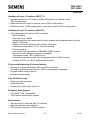
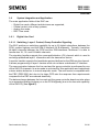
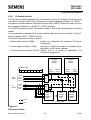
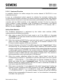
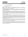
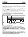
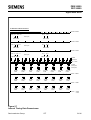
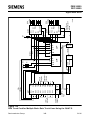
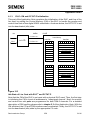
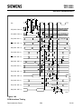
Overview
1
Overview
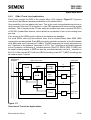
The PEB 20550 (Extended Line Card Controller) is a highly integrated controller circuit
optimized for line card and key system applications. It combines all functional blocks
necessary to manage up to 32 digital (ISDN or proprietary) or 64 analog subscribers.
The switching and layer-1 control capability of the EPIC-1 (PEB 2055) constitutes a
major functional block of the ELIC.
For layer-2 support, two independent Special Application Communication Controllers
(SACCO) are available. One typically handles the communication with the group
controller, the other is used to serve the subscriber terminals. A D-channel arbiter is
employed to multiplex the HDLC controller between multiple subscribers while
maintaining full duplex signaling protocols (e.g. LAPD).
Additionally, typical line card glue logic functions such as a power-up reset generator, a
watchdog timer and two parallel ports are integrated.
The ELIC is implemented in a Siemens advanced 1.0-µm CMOS-technology and
manufactured in a P-MQFP-80-1 package.
The ELIC is a member of a new chip family supporting D-channel multiplexing on the line
card and in the subscriber terminal. This concept allows an highly economical
implementation of digital subscriber lines.
Chip Family
Line Cards:
PEB 20550
PEB 2096
PEB 2095
PEB 2084
PEB 2465
PEB 2075
Extended Line Card Controller
Octal UPN Transceiver
ISDN Burst Transceiver Circuit
QUAD S0 Transceiver
QUAD DSP based Codec Filter
ISDN D-Channel Exchange Controller
(ELIC)
(OCTAT-P)
(IBC)
(QUAT-S)
(SICOFI-4)
(IDEC)
PSB 2196
Digital Subscriber Access Controller
for UPN Interface
(ISAC-P TE)
PEB 2081 (V3.2)
S/T-Bus Interface Circuit Extended
(SBCX)
Terminals:
Semiconductor Group
11
01.96
PEB 20550
PEF 20550
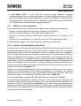
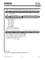
Overview
R
IOM -2
2048 kbit/s
TE 0
8xS
S0
TE 7
QUAT-S
PEB 2084
PCM
0
PCM
R
ELIC
PEB 20550
TE 0
8 x U PN
CFI
0
R
U PN
TE 7
OCTAT -P
PEB 2096
1
D Arbiter
TE 1
16 x t/r
r/t
TE 16
2
SLIC
SLIC
R
SICOFI -4
PEB 2465
SACCO-A
3
SACCO-B
TSS
Signaling
8xT
0
CO
7
R
Memory
IOM -2
QUAT-S
PEB 2084
µP Interface
R
µP
IOM -2
4 x D Cannel
R
IDEC
PEB 2075
ITB05392
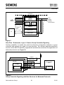
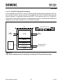
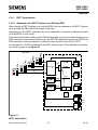
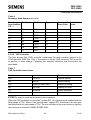
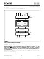
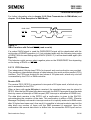
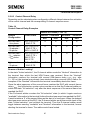
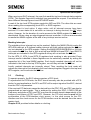
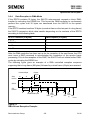
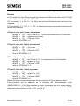
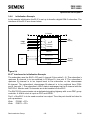
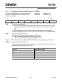
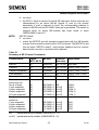
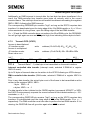
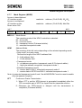
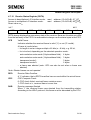
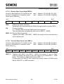
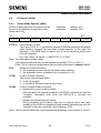
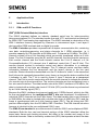
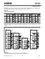
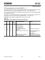
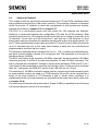
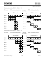
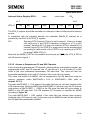
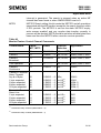
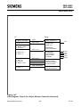
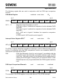
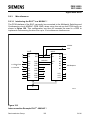
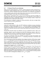
Figure 1
Example for an Integrated Analog / Digital PBX
Semiconductor Group
12
01.96
Extended Line Card Interface Controller
ELIC®
PEB 20550
PEF 20550
Versions 1.3
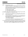
1.1
CMOS
Features
Switching (EPIC®-1)
• Non-blocking switch for 32 digital (e.g. ISDN) or
64 voice subscribers
– Bandwidth 16, 32, or 64 kbit/s
– Two consecutive 64-bit/s channels can be
P-MQFP-80-1
switched as a single 128-kbit/s channel
• Freely programmable time slot assignment for all
subscribers
• Synchronous µP-access to two selected channels
• Two types of serial interfaces independently programmable over a wide data range
(128 - 8192 kbit/s)
– PCM-interface
Tristate control signals for external drivers
Programmable clock shift
Single or double data clock
– Configurable interface
Configurable for IOM-, SLD- and PCM-applications
High degree of flexibility for datastream adaption
Programmable clockshift
Single or double data clock
Type
Ordering Code
Package
PEB 20550
Q67101-H6484
P-MQFP-80-1 (SMD)
PEF 20550
Q67101-H6605
P-MQFP-80-1 (SMD)
Semiconductor Group
13
01.96
PEB 20550
PEF 20550
Overview
Handling of Layer-1 Functions (EPIC®-1)
• Change detection for C/I-channel (IOM-configuration) or feature control
(SLD-configuration)
• Additional last-look logic for feature control (SLD-configuration)
• Buffered monitor (IOM-configuration) or signaling channel (SLD-configuration)
Handling of Layer-2 Functions (SACCO)
• Two independent full duplex HDLC-channels
– Serial interface
Data rate up to 4 Mbit/s
Independent time slot assignment for each channel with programmable time slot
length (1-256 bits)
Support of bus configuration with collision resolution
Continuous transmission of 1 to 32 bytes possible
– Protocol support
Auto-mode, fully compatible to PEB 2050 (PBC) protocol
Non-auto mode, address recognition capability
Transparent mode, HDLC-framing only
Extended transparent mode, fully transparent without HDLC-framing
– 64-bytes FIFO’s per HDLC-channel and direction
D-channel Multiplexing (D-channel arbiter)
•
•
•
•
Serving of multiple subscribers with one HDLC-controller
Full duplex signaling protocols (e.g. LAPD or proprietary) supported
Programmable priority scheme
Broadcast transmission
Line Card Glue Logic
• Power-up reset generator
• Watchdog timer
• Parallel ports (8-bit input, 4-bit I/O)
Boundary Scan Support
• Fully IEEE 1149.1 compatible
• 32-bit device identification register
Bus Interface
• Siemens/Intel or Motorola type µP-interface
• 8-bit demultiplexed bus interface
• FIFO-access interrupt or DMA controlled
Semiconductor Group
14
01.96
PEB 20550
PEF 20550
Overview
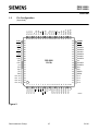
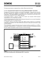
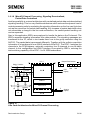
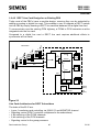
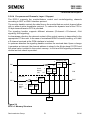
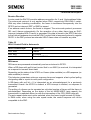
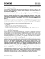
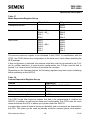
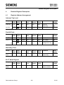
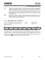
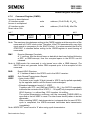
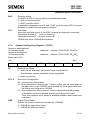
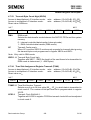
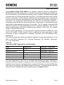
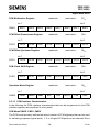
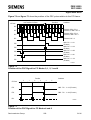
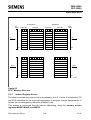
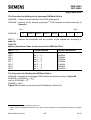
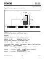
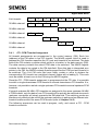
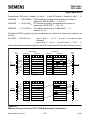
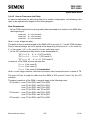
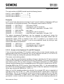
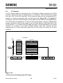
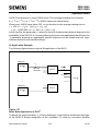
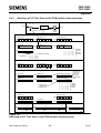
Pin Configuration
(top view)
RxD 1
RxD 2
RxD 3
VSS
RxDB
CxDB
TxDB
TSCB
HDCB
VDD
HFSB
HFSA
HDCA
TSCA
TxDA
CxDA
RxDA
DRQTA
DRQRA
DRQTB
1.2
60 59 58 57 56 55 54 53 52 51 50 49 48 47 46 45 44 43 42 41
RxD0
TSC0
TxD0
TSC1
TxD1
TSC2
TxD2
TSC3
TxD3
PFS
PDC
VSS
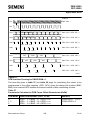
TCK
TDO
TDI
TMS
P0.0, A0
P0.1, A1
P0.2, A2
P0.3, A3
61
62
63
64
65
66
67
68
69
70
71
72
73
74
75
76
77
78
79
80
PEB 20550
ELIC R
40
39
38
37
36
35
34
33
32
31
30
29
28
27
26
25
24
23
22
21
DRQRB
DACKA
DACKB
DD3/SIP3
DD2/SIP2
DD1/SIP1
DD0/SIP0
DU3/SIP7
DU2/SIP6
VSS
DU1/SIP5
DU0/SIP4
DCL
FSC
RESEX
RESIN
P1.3
P1.2
P1.1
P1.0
P0.4, A4
P0.5, A5
P0.6, A6
P0.7, A7
INT
CSE
CSS
WR, R/W
RD, DS
ALE
VDD
AD0, D0
AD1, D1
AD2, D2
AD3, D3
AD4, D4
AD5, D5
AD6, D6
AD7, D7
VSS
1 2 3 4 5 6 7 8 9 10 11 12 13 14 15 16 17 18 19 20
ITP05803
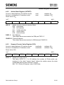
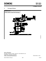
Figure 2
Semiconductor Group
15
01.96
PEB 20550
PEF 20550
Overview
1.3
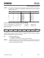
Pin Definitions and Functions
µ-Processor Interface
Pin No.
Symbol
Input (I)
Function
Output (O)
6
CSE
I
Chip Select EPIC-1; active low. A "low" on this line
selects all registers (excluding the SACCOregisters) for read/write operations.
7
CSS
I
Chip Select SACCO; active low. A "low" on this
line selects the SACCO-registers for read/write
operations.
8
WR,
R/W
I
Write, active low, Siemens/Intel bus mode.
When "low", a write operation is indicated.
Read/Write, Motorola bus mode.
When "high" a valid µP-access identifies a read
operation, when "low" it identifies a write access.
9
RD, DS
I
Read, active low, Siemens/Intel bus mode.
When "low" a read operation is indicated.
Data Strobe, Motorola bus mode.
A rising edge marks the end of a read or write
operation.
12
13
14
15
16
17
18
19
AD0, D0
AD1, D1
AD2, D2
AD3, D3
AD4, D4
AD5, D5
AD6, D6
AD7, D7
I/O
I/O
I/O
I/O
I/O
I/O
I/O
I/O
Address/Data Bus; multiplexed bus mode.
Transfers addresses from the µP-system to the
ELIC and data between the µP and the ELIC.
Data Bus; demultiplexed bus mode.
Transfers data between the µP and the ELIC.
When driving data the pins have push pull
characteristic, otherwise they are in the state
high impedance.
10
ALE
I
Address Latch Enable
ALE controls the on chip address latch in
multiplexed bus mode. While ALE is "high", the
latch is transparent. The falling edge latches the
current address. During the first read/write access
following reset ALE is evaluated to select the bus
mode.
Semiconductor Group
16
01.96
PEB 20550
PEF 20550
Overview
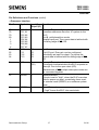
Pin Definitions and Functions (cont’d)
µ-Processor Interface
Pin No.
Symbol
Input (I)
Function
Output (O)
77
78
79
80
1
2
3
4
P0.0,A0
P0.1,A1
P0.2,A2
P0.3,A3
P0.4,A4
P0.5,A5
P0.6,A6
P0.7,A7
I
I
I
I
I
I
I
I
Address Bus, demultiplexed bus mode.
Transfers addresses from the µP-system to the
ELIC.
Port 0, multiplexed bus mode.
Parallel input port. The current data is latched with
the falling edge of RD, DS.
21
22
23
24
P1.0
P1.1
P1.2
P1.3
I/O
I/O
I/O
I/O
Port 1
4-bit I/O port. Every pin can be configured
individually as input or output. For inputs the
current data is latched with the falling edge of RD,
DS.
5
INT
O
(OD)
Interrupt Request, active low.
This signal is activated when the ELIC requests an
interrupt. Due to the open drain (OD)
characteristic of INT multiple interrupt sources can
be connected together.
25
RESIN
O
Reset Indication
This pin is set to "high", when the ELIC executes
either a power-up reset, a watchdog timer reset,
an external reset (RESEX) or a software system
reset.
26
RESEX
I
Reset External
A "high" forces the ELIC into reset state.
Semiconductor Group
17
01.96
PEB 20550
PEF 20550
Overview
Pin Definitions and Functions (cont’d)
EPIC®-1 Interface
Pin No.
Symbol
Input (I)
Function
Output (O)
70
PFS
I
PCM-Interface Frames Synchronization
71
PDC
I
PCM-Interface Data Clock
Single or double data rate.
61
60
59
58
RxD0
RxD1
RxD2
RxD3
I
I
I
I
Receive PCM-Interface Data
Time-slot oriented data is received on this pins
and forwarded into the downstream data memory
of the EPIC-1.
63
65
67
69
TxD0
TxD1
TxD2
TxD3
O
O
O
O
Transmit PCM-Interface Data
Time-slot oriented data is shifted out of the
EPIC-1s upstream data memory on this lines. For
time-slots which are flagged in the tristate data
memory or when bit OMDR:PSB is reset the
pins are set in the state high impedance.
62
64
66
68
TSC0
TSC1
TSC2
TSC3
O
O
O
O
Tristate Control
Supplies a control signal for an external driver.
These lines are "low" when the corresponding
TxD-outputs are valid. During reset these lines are
"high".
27
FSC
I/O
Frame Synchronization
Input or output in IOM-configuration. Direction
indication signal in SLD-mode.
28
DCL
I/O
Data Clock
Input or output in IOM, slave clock in SLD
configuration. In IOM-configuration single or
double data rate, single data rate in SLD-mode.
Semiconductor Group
18
01.96
PEB 20550
PEF 20550
Overview
Pin Definitions and Functions (cont’d)
EPIC®-1 Interface
Pin No.
Symbol
Input (I)
Function
Output (O)
29
30
32
33
DU0/SIP4
DU1/SIP5
DU2/SIP6
DU3/SIP7
I/IO (OD)
I/IO (OD)
I/IO (OD)
I/IO (OD)
Data Upstream Input; IOM- or PCM-configuration.
Serial Interface Port, SLD-configuration.
Depending on the bit OMDR:COS these lines
have push pull or open drain characteristic.
For unassigned channels or when bit
OMDR:CSB is reset the pins are in the state
high impedance.
34
35
36
37
DD0/SIP0
DD1/SIP1
DD2/SIP2
DD3/SIP3
O/IO (OD)
O/IO (OD)
O/IO (OD)
O/IO (OD)
Data Downstream Output, IOM- or PCMconfiguration.
Serial Interface Port, SLD-configuration.
Depending on the bit OMDR:COS these lines
have push pull or open drain characteristic.
For unassigned channels or when bit
OMDR:CSB is reset the pins are in the state
high impedance.
Semiconductor Group
19
01.96
PEB 20550
PEF 20550
Overview
Pin Definitions and Functions (cont’d)
SACCO-Interface
Pin No.
Symbol
Input (I)
Function
Output (O)
49
50
HFSA
HFSB
I
I
HDLC-Interface Frame Synchronization
Channel A/B
Frame synchronization pulse in clock mode 2,
data strobe in clock mode 1.
48
52
HDCA
HDCB
I
I
HDLC-Interface Data Clock Channel A/B. Single
or double data rate.
44
56
RxDA
RxDB
I
I
Receive Serial Data HDLC-Channel A/B
The serial data received on this lines is forwarded
into the corresponding HDLC-receive channel.
Data is sampled on the
– falling edge of HDC (CCR2:RDS = 0) or
– rising edge of HDC (CCR2:RDS = 1).
46
54
TxDA
TxDB
O (OD)
O (OD)
Transmit Serial Data HDLC-Channel A/B.
Data output lines of the corresponding HDLCtransmit channel. Depending on the bit
CCR1:ODS the pins have push pull or open
drain characteristic. When transmission is
disabled (TSCA or B = 1) or when bit
CCR2:TXDE is reset the pins are in the state
high impedance.
47
53
TSCA
TSCB
O
O
Tristate Control HDLC-Channel A/B, active low.
Supplies a control signal for an external driver.
When low the corresponding TxD-outputs are
valid. The detailed functionality is defined
programming the SACCO-registers
CCR2:SOC1,SOC0. During reset these lines are
high.
45
55
CxDA
CxDB
I
I
Collision Data HDLC-Channel A/B
In a bus configuration, the external serial bus must
be connected to the respective CxD-pin for
collision detection.
In point-to-point configurations the pin provides a
"clear to send" function. When '0'/'1' the transmit
channel is enabled/disabled. If this function is
not needed CxDA/B has to be tied to VSS.
Semiconductor Group
20
01.96
PEB 20550
PEF 20550
Overview
Pin Definitions and Functions (cont’d)
SACCO-Interface
Pin No.
Symbol
Input (I)
Function
Output (O)
42
40
DRQRA
DRQRB
O
O
DMA-Request Receiver Channel A/B
The receiver of HDLC-channel A/B requests a
DMA-data transfer by activating this lines. The
DRQR-pin remains "high" as long as the receiver
FIFO requires data transfers. Only blocks of 32,
16, 8 or 4 bytes are transferred.
43
41
DRQTA
DRQTB
O
O
DMA-Request Transmitter Channel A/B
The transmitter of HDLC-channel A/B requests a
DMA-data transfer by activating this lines. The
DRQT-pin remains "high" as long as the transmit
FIFO requires data transfers. The number of data
bytes to be transferred from system memory to the
FIFO must be written first into the XBCH, XBCL
registers (byte count registers).
39
38
DACKA
DACKB
I
I
DMA-Acknowledge HDLC-Channel A/B, active
low.
When "low", this lines notifies the HDLC-channel,
that the requested DMA-cycle is in progress.
Together with RD (DRQR) or WR(DRQT) DACK
works like CS to enable a read or write operation
to the top of the receive or the transmit FIFO.
When DACK is active, the address lines are
ignored and the FIFOs are implicitly selected.
When DACK is not used it has to be connected to
VDD.
Semiconductor Group
21
01.96
PEB 20550
PEF 20550
Overview
Pin Definitions and Functions (cont’d)
Boundary Scan Interface, according to IEEE Std. 1149.1
Pin No.
Symbol
Input (I)
Function
Output (O)
76
TMS
I
(internal
pull-up)
Test Mode Select
A 0 -> 1 transition on this pin is required to step
through the TAP-controller state machine.
75
TDI
I
(internal
pull-up)
Test Data Input
In the appropriate TAP-controller state test data or
a instruction is shifted in via this line
74
TDO
O
Test Data Output
In the appropriate TAP-controller state test data or
a instruction is shifted out via this line.
73
TCK
I
Test Clock
Single rate test data clock.
Note: Pin 75 (TDI) and pin 76 (TMS) are internally connected to VDD via pull-up resistors.
Semiconductor Group
22
01.96
PEB 20550
PEF 20550
Overview
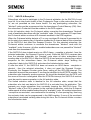
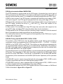
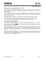
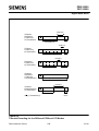
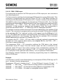
1.4
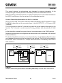
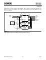
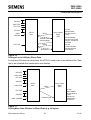
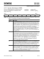
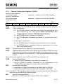
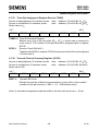
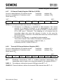
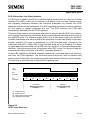
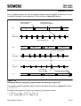
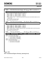
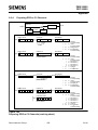
Logic Symbol
Boundary Scan Interface
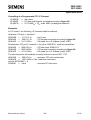
TMS TCK TDI TDO
FSC
DCL
CFI
Port 0
DD 0
DU 0
CFI
Port 1
DD 1
DU 1
CFI
Port 2
DD 2
DU 2
CFI
Port 3
DD 3
DU 3
HDLC
Channel B
DMA
Interface
Channel B
PFS
PDC
ELIC
R
HFSB
HDCB
CxDB
RxDB
TxDB
TSCB
DRQRB
DRQTB
DACKB
RESEX
RESIN
WR,
R or RD, AD 0-7,
INT CSE CSS ALE W DS D 0-7
P 0.0-0.7,
A 0-7
RxD 0
TxD 0
TSC 0
PCM
Highway 0
RxD 1
TxD 1
TSC 1
PCM
Highway 1
RxD 2
TxD 2
TSC 2
PCM
Highway 2
RxD 3
TxD 3
TSC 3
PCM
Highway 3
HFSA
HDCA
CxDA
RxDA
TxDA
TSCA
HDLC
Channel A
DRQRA
DRQTA
DACKA
DMA
Interface
Channel A
P 1.0-1.3
ITL05804
Bus Interface
Figure 3
Semiconductor Group
23
01.96
PEB 20550
PEF 20550
Overview
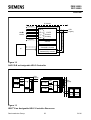
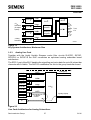
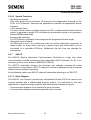
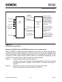
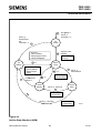
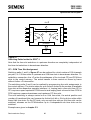
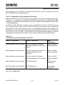
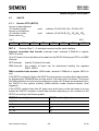
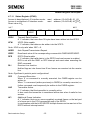
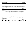
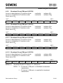
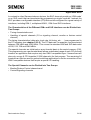
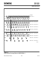
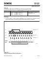
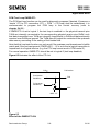
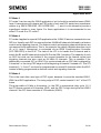
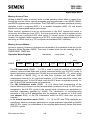
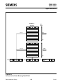
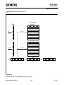
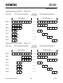
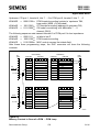
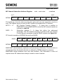
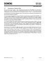
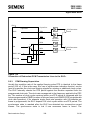
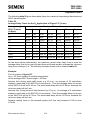
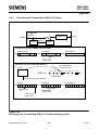
Functional Block Diagram
Serial Interface B Serial Interface A
FSC
DCL
R
IOM -2
Port 3
R
IOM -2
Port 2
R
IOM -2
Port 1
R
IOM -2
Port 0
1.5
D-Channel Arbiter
Watch
Dog
Timer
RESEX
RESIN
TMS
TCK
TDI
TDO
Powerup
Reset
Generator
PFC
PDC
PCM
Highway 0
SACCO-B
SACCO-A
PCM
Highway 1
R
EPIC -1
PCM
Highway 2
Boundary
Scan
Controller
PCM
Highway 3
Bus Interface Unit
DMA
Interface A
DMA
Interface B
INT CSE CSS ALE RD WR,
DS R or
WR
P 0.0-7, AD 0-7,
A 0-7
D 0-7
P 1.0-1.3
ITB05805
Figure 4
Semiconductor Group
24
01.96
PEB 20550
PEF 20550
Overview
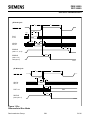
1.6
System Integration and Application
The main application fields of the ELIC are:
–
–
–
–
Digital line cards, different architectures are supported,
Central control units of key systems,
Analog line cards,
DECT line cards.
1.6.1
Digital Line Card
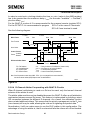
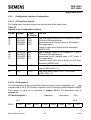
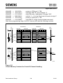
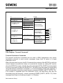
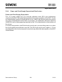
1.6.1.1 Switching, Layer-1 Control, Group Controller Signaling
The ELIC performs a switching capability for up to 32 digital subscribers between the
PCM- system highway and the IOM-2 interface (64 B-channels). Typically it switches
64-kbit/s channels between the PCM and the IOM-interfaces. Moreover it is able to
handle also 16-, 32- and 128-kbit/s channels.
The signaling handler supports the command/indication (C/I) channel which is used to
exchange predefined layer-1 information with the transceiver device.
A monitor handler supports the handshake protocol defined on the IOM-monitor channel.
It allows programming of layer-1 devices which do not have a dedicated µP interface.
The communication between the line card and the group controller is performed by one
of the SACCO-channels. Its auto-mode is optimized for this application and implements
a slave station behaviour in normal response mode. The auto-mode is compatible with
the PBC (PEB 2050) but due to the large FIFO-size the response time requirements
compared to the PBC are reduced drastically.
The data exchange between the line card and the group controller board can take place
on a separate signalling highway or on the PCM-highway (due to the time slot capability
of the SACCO) (see figure 5).
Semiconductor Group
25
01.96
PEB 20550
PEF 20550
Overview
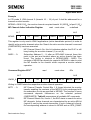
B Channels
PCM
Highway
Switching
R
IOM -2
Interface
EPIC
R
Signaling
Handler
C/I, Monitor
Channel
Signaling,
Group Controller
Monitor
Handler
ARBITER
SACCO CH-A
µP
SACCO CH-B
ELIC
R
ITS05806
Figure 5
Data Flow - B-channels, Layer-1 Control, Group Controller Signaling
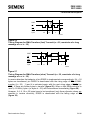
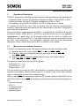
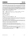
Another possibility to handle the point-to-multi-point configuration between a group
controller and several line cards is a bus structure. The collision detection/resolution
function of the SACCO perfectly supports this architecture and allows the application of
balanced protocols (see figure 6).
Transmit
Collision Input
Receive
Line Card
ELIC
Group Controller
Board
R
HSCX
SACCO CH-B
ITS05807
Figure 6
Group Controller Signaling with Bus Structure for Balanced Protocols
Semiconductor Group
26
01.96
PEB 20550
PEF 20550
Overview
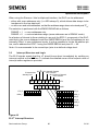
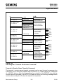
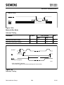
D-channel processing is supported by multiple different architectures:
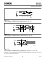
1.6.1.2 Decentralized D-Channel Processing, Multiplexed HDLC-Controller.
Typically the D-channel load has a very bursty characteristic. Taking this into account,
the ELIC provides the capability to multiplex one HDLC-controller among several
subscribers. This feature results in a drastical reduction of hardware requirements while
maintaining all benefits of HDLC based signaling.
A D-channel arbiter is used to assign the receive and transmit HDLC-channel
independently to the subscriber terminals.
In downstream direction the arbiter links the transmit channel to one or more (broadcast)
programmable IOM-2 D-channels (ports).
In upstream direction the arbiter assigns the HDLC-receive channel to a requesting
subscriber and indicates to all other subscribers that their D-channels are blocked, using
a control channel.
This configuration supports full duplex layer-2 protocols with bus capability e.g. LAPD or
proprietary implementations. Consequently no polling overhead is necessary providing
the full 16-kbit/s bandwidth of the D-channel for data exchange.
B Channels
R
IOM -2
Interface
EPIC
PCM
Highway
R
D Channel
Controlling
D Channel
ARBITER
SACCO CH-A
µP
Signaling
Highway
SACCO CH-B
ELIC
R
ITS05808
Figure 7
D-Channel Handling with a Multiplexed HDLC-controller
Semiconductor Group
27
01.96
PEB 20550
PEF 20550
Overview
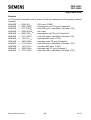
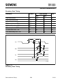
The control channel is unidirectional and forwards the status information of the
corresponding D-channel (blocked or available) towards the subscriber terminal.
Different existing channel structures are used to implement the control channel between
the HDLC-controllers on the line card and in the subscriber terminal.
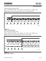
Control Channel Implementation on the U PN-Interface
On an UPN-line card, the control channel is either integrated in the C/I-channel or uses
the MR-bit, depending on the connected layer-1 device (OCTAT-P -> C/I channel, IBC
-> MR-bit).
The UPN-transceiver uses the T-channel to transmit the control channel information to the
terminal. The T-channel is a sub channel of the UPN-interface with a bandwidth of 2 kbit/
s.
In the subscriber terminal the control channel is included again in the IOM-2 protocol.
Depending on the terminal configuration two alternatives can be selected in the terminal
transceiver device.
The blocked/available information is translated directly into the S/G-bit (Stop/Go) when
no subsequent transceiver circuit is present in the terminal. The S/G-bit is evaluated by
the terminal HDLC-controller ICC. It stops data transmission immediately when the S/
G-bit is set to 1.
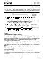
S/G = 1
S/G = 0
Blocked
Available
T=0
T=1
Blocked
Available
S/G
ICC
(optional)
MR = 0
MR = 1
T
U p0
Transceiver
Blocked
Available
MR
IBC
ELIC
R
HDLC Controller
DSAC-P
ITS05809
Figure 8
Control Channel Implementation with IBC (PEB 2095) as Line Card Transceiver
Semiconductor Group
28
01.96
PEB 20550
PEF 20550
Overview
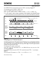
In figure 9 a Control Channel Implementation with OCTAT-P as line card transceiver
can be seen.
When an additional transceiver device is integrated in the terminal (e.g. an S0-adapter,
PEB 2081 (SBCX)) the control channel is translated into the A/B-bit (bit5, 4th byte,
IOM-channel 2, downstream). The A/B-bit is monitored by the SBCX. A/B = 1 indicates
that the corresponding D-channel is available (A/B = 0 blocked). Depending on this
information, the SBCX controls the E-bit on the S0-bus and the S/G-bit on the IOM-2
interface. When A/B = 0 the E-bit is forced in the inverted D-bit state, the S/G-bit is set
to high. As a result all active transmitters in the terminal and on the S0-bus are forced to
abandon their messages.
A/B = 0
A/B = 1
E
Blocked
Available
T=0
T=1
A/B
SBCX
S/G
ICC
(optional)
Blocked
Available
C/I = 1100
C/I = 1000
T
U p0
Transceiver
Blocked
Available
C/I
R
OCTAT -P
ELIC
R
HDLC Controller
DSAC-P
ITS05810
Figure 9
Control Channel Implementation with OCTAT®-P (PEB 2096) as Line Card
Transceiver and S0-Adapter.
Semiconductor Group
29
01.96
PEB 20550
PEF 20550
Overview
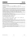
Control Channel Implementation on the S0-Interface
When using the ELIC on a S0-line card the structure is much simpler because the
S0-interface provides contention resolution as a standard feature. In this structure the
QUAT-S modifies the E-bit on the line card, i.e. standard S0-phones can be connected.
The control channel on the line card is included in the C/I-channel.
S0 Phone
S0 Phone
C/I = 1100
C/I = 1000
Blocked
Available
C/I
E
S0
S0 Phone
S0 Phone
R
QUAT -S
ELIC
R
E
S0
ITS05811
Figure 10
Control Channel Implementation on a S 0-Line Card
Even with a multiplexed HDLC controller signaling and packet data can be mixed on a
S0 line card. The priority scheme of the S0 bus (2 priority classes) guarantees, that signal
data is not delayed by data packets.
Semiconductor Group
30
01.96
PEB 20550
PEF 20550
Overview
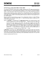
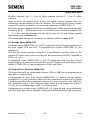
1.6.1.3 Decentralized D-Channel Processing, Dedicated HDLC-Controller per
Subscriber
In this configuration IDECs (ISDN D-channel exchange controller, PEB 2075) handle the
layer-2 functions for signaling and data packets in the D-channel. The extracted data is
separated and sent via the µP and the SACCO to the system interface. In this
configuration signaling data is transferred on the PCM-highway, for packet data a
dedicated bus system with collision resolution is used.
Example Frame Structure
B
R
IOM -2 Interface
EPIC
s+p
Data
IDEC
R
IDEC
B
...
B
B
B
S
B
PCM
Highway
R
R
ARBITER
s-Data
SACCO CH-A
s-Data
µP
Packet Highway with
Collision Resolution
SACCO CH-B
p-Data
ELIC
R
ITS05812
Figure 11
Line Card Architecture for Completely Decentralized D-Channel Processing
1.6.1.4 Decentralized D-Channel Processing, Multiplexed plus Dedicated
HDLC-Control
Especially when packet data is supported in the D-channel one multiplexed HDLC
controller may create a bottleneck situation. One solution to overcome this problem is
the combination of the multiplexing scheme with additional layer-2 controllers which can
be temporarily assigned to individual subscribers on request.
In normal operation all subscribers are managed by the D-channel arbiter and share
SACCO-A. When a subscriber requests a special type of service, the system can switch
a dedicated HDLC controller and exclude this subscriber temporarily from the arbitration.
For small systems SACCO-B, for bigger systems IDECs may be used as an assignable
controller resource.
Semiconductor Group
31
01.96
PEB 20550
PEF 20550
Overview
B Channels
D Channel
EPIC
R
IOM -2
Interface
PCM
Highway
R
D Channel
Controlling
D Channel
ARBITER
SACCO CH-A
Shared HDLC Controller
µP
SACCO CH-B
Dedicated HDLC Controller
ELIC
R
ITS05813
Figure 12
SACCO-B as Assignable HDLC-Controller
PCM
Highway
R
IOM -2
R
OCTAT -P
PCM
Highway
R
ELIC
IOM -2
R
IOM -2
R
R
OCTAT -P
R
OCTAT -P
R
IOM -2
ELIC
R
R
IDEC
R
OCTAT -P
IDEC
R
IDEC
R
IDEC
R
IDEC
R
ITS05814
Figure 13
IDEC®-S as Assignable HDLC-Controller Resources
Semiconductor Group
32
01.96
PEB 20550
PEF 20550
Overview
1.6.1.5 Central D-Channel Processing
In this application the EPIC-1 not only switches the B-channels and performs the C/Iand monitor channel control function, but switches also the D-channel data onto the
system highway. In upstream direction the EPIC-1 can combine up to four 16-kbit/s Dchannels into one 64-kbit/s channel. In downstream direction it provides the capability to
distribute one 64-kbit/s channel in four 16-kbit/s channels.
B, D
Example Frame Structure
B
R
IOM -2
Interface
EPIC
B
...
B
DDDD
B
PCM
Highway
R
ARBITER
SACCO CH-A
µP
Signaling Highway for
Line Card Control
SACCO CH-B
ELIC
R
ITS05815
Figure 14
Line Card Architecture for Completely Centralized D-Channel Processing
Semiconductor Group
33
01.96
PEB 20550
PEF 20550
Overview
1.6.1.6 Mixed D-Channel Processing, Signaling Decentralized,
Packet Data Centralized
Another possibility is a mixed architecture with centralized packet data and decentralized
signaling handling. This is a very flexible architecture which reduces the dynamic load of
central processing units by evaluating the signaling information on the line card, but does
not require resources for packet data handling. Any increase of packet data traffic does
not necessitate a change in the line card architecture, the central packet handling unit
can be expanded.
Also in this application IDECs are employed to handle the data on the D-channel. The
IDECs separate signaling information from data packets. The signaling messages are
transferred to the µP, which in turn hands them over to the group controller using the
SACCO. The packet data is processed differently. Together with the collision resolution
information it is transferred to one IOM-2 interface of the ELIC. The EPIC-1 switches the
channels to the PCM-highway, optionally combining four D-channels to one 64-kbit/s
channel. In this configuration one IOM-2 interface is occupied by IDECs, reducing the
total switching capability of the EPIC-1 to 24 ISDN-subscribers.
B, P, C
Example Frame Structure
B
R
IOM -2 Interface
p-Data
EPIC
P+Coll
B
...
B
P B C B
Packet Collision
Data
Data
PCM
Highway
R
P
Sig.
Data
IDEC
R
IDEC
R
ARBITER
SACCO CH-A
Signaling
S
SACCO CH-B
µP
ELIC
Signaling
Highway
R
ITS05816
Figure 15
Line Card Architecture for Mixed D-Channel Processing
Semiconductor Group
34
01.96
PEB 20550
PEF 20550
Overview
Alternatively, the packet and collision data can be directly exchanged between the
IDECs and the PCM-highway. Thus, the full 32 subscriber switching capability of the
EPIC-1 is retained.
B
R
IOM -2
Interface
s + p-Data
ELIC
PCM
Highway
R
Coll
Signaling
S
Packet Data
µP
Signaling
Highway
P
P
R
IDEC
Signaling
Packet Data
R
IDEC
Signaling
P
P
Coll
ITS05817
Figure 16
Line Card Architecture for Mixed D-Channel Processing
Semiconductor Group
35
01.96
PEB 20550
PEF 20550
Overview
1.6.2
Key Systems
The ELIC is an optimal solution for key systems like a PBX. When selecting the
multiplexed D-channel architecture, the ELIC covers switching, layer-1 and layer-2
control for the entire system. Together with the IOM-2 compatible Siemens transceiver
circuits, a complete key system can be build with a few devices.
S0
Trunk
R
IOM -2
S0
R
QUAT -S
S0
3 S0
Subscribers
R
IOM -2
ELIC
S0
R
SACCO_A
S0 Subscribers
4 Analog
Subscriber
R
SICOFI -4
SACCO_B
Trunk
ITS05818
Figure 17
Key System Architecture, Small Size
R
IOM -2
8 U p0
Subscribers
(S 0 adapter
optional)
R
.
.
.
R
IOM -2
S0
ISAC -S
R
OCTAT -P
SACCO_A
Subscriber
R
2 Analog
Subscribers
ELIC
R
IOM -2
R
SICOFI -2
R
S0
Trunk,
2 S0
ISAC -S
SACCO_B
Assignable
ITS05819
Figure 18
Key System Architecture, Medium Size
Semiconductor Group
36
01.96
PEB 20550
PEF 20550
Overview
R
IOM -2
R
OCTAT -P
8 U p0
Subscribers
(S 0 adapter
optional)
ELIC
IDEC
R
R
S0
R
IOM -2
R
OCTAT -P
SACCO_A
Subscriber
S0
R
QUAT -S
R
IOM -2
R
OCTAT -P
SACCO_B
Assignable
S0
Trunk,
4 S0
S0
R
IOM -2
4 Analog
Subscribers
R
SICOFI -4
ITS05820
Figure 19
Key System Architecture, Maximum Size
1.6.3
Analog Line Card
Together with the highly flexible Siemens codec filter circuits SLICOFI, SICOFI,
SICOFI-2 or SICOFI-4 the ELIC constitutes an optimized analog subscriber board
architecture.
The EPIC-1 part of the ELIC handles the signalling and voice data for up to 64 subscriber
channels with 64 kbit/s. The SACCO establishes the link to the group controller board.
B Channels
PCM Highway
R
R
IOM -2
SICOFI -4
R
SICOFI -4
R
R
IOM -2
SICOFI -4
R
SICOFI -4
R
R
IOM -2
SICOFI -4
ELIC
R
R
SICOFI -4
R
R
IOM -2
SICOFI -4
Signaling Highway
R
SICOFI -4
C/I, Monitor
Channel
µP
ITS05821
Figure 20
Line Card Architecture for Analog Subscribers
Semiconductor Group
37
01.96
PEB 20550
PEF 20550
Overview
1.6.4
DECT Applications
1.6.4.1 Adaptation of a DECT System to an Existing PBX
When adding a DECT system to an existing PBX, the line interface of the DECT system
must provide the PBX with PCM-coded voice data.
Depending on the DECT controller the voice information is carried in different formats
(4 bit ADPCM or 8 bit PCM ).
Therefore a base station offering 8 bit PCM coded data can be connected directly to any
PBX, whereas a base station delivering 4 bit ADPCM coded data needs an ADPCM to
PCM converter. Such an adapter is called Common Control Fixed Part (CCFP).
An example for a CCFP realized with the ELIC (serving up to 32 handhelds in operation
at a time) is given in the figure 21.
Base Stations
CCFP
SYNC
4
3
R
IOM -2
2
R
QUAD
ADPCM
ADPCM
R
OCTAT -P
1
ELIC
D
UPN
PCM
QUAD
ADPCM
R
R
IOM -2
R
IOM -2
SICOFI -4
R
SICOFI -4
HDLC HDLC
DSP
µC
SLIC
32xt/r
Trunk
SLIC
ITS07314
Figure 21
DECT Application
Semiconductor Group
38
01.96
PEB 20550
PEF 20550
Overview
In this configuration the base stations are connected to the line interface of the CCFP via
UPN (OCTAT-P). The 4 bit ADPCM voice channels provided by the base stations are
switched (by the ELIC) to the PCM - ADPCM converter (QUAD ADPCM), expanded to
an 8 bit ADPCM value and then switched (by the ELIC) to the analog trunk interface
(SICOFI-4 + SLIC).
The additional DSPs are necessary, to compensate short end echoes occurring at
analog nodes
The line card controller ELIC (PEB 20550) fulfills four major tasks:
•
•
•
•
Layer-1 monitoring and controlling via IOM-2 C/I and MONITOR channel
Signaling control (HDLC controller multiplexed to the subscribers)
4 bit switching of the PCM4 channels
8 bit switching of the PCM channels
Semiconductor Group
39
01.96
PEB 20550
PEF 20550
Overview
1.6.4.2 DECT Line Card Design for an Existing PBX
Today most of the PBX´s have a modular design, meaning they can be extended by
adding an analog or digital line card. This enables a user to integrate a DECT system
into his PBX by simply inserting a DECT line card that behaves like a digital line card.
To communicate over the existing PCM highway, a PCM4 to PCM converter must be
integrated onto the line card.
Compared to a digital line card a DECT line card requires additional efforts to
synchronize all line cards.
v
Base Stations
DECT Line Card
4
SYNC
3
ELIC
R
IOM -2
2
QUAD
ADPCM
ADPCM
R
OCTAT -P
1
R
D
UPN
QUAD
ADPCM
PCM
PCM
HDLC HDLC
DSP
Signaling
Highway
µC
2 Mbit/s
PCM
Highway
ITS07315
Figure 22
Line Card Architecture for DECT Subscribers
The tasks of the ELIC are:
•
•
•
•
•
Layer-1 monitoring and controlling via IOM-2 C/I and MONITOR channel
Signaling control (HDLC controller multiplexed to the subscribers)
4 bit switching of the PCM4 channels
8 bit switching of the PCM channels
Signaling control to the group processor
Semiconductor Group
40
01.96
PEB 20550
PEF 20550
Functional Description
2
Functional Description
2.1
General Functions and Device Architecture
The ELIC integrates the existing Siemens device PEB 2055 (EPIC-1), a two channel
HDLC-Controller (SACCO: Special Application Communication Controller) with a
PEB 2050 (PBC) compatible auto-mode, a D-channel arbiter, a configurable bus
interface and typical system glue logic into one chip. It covers all control functions on
digital and analog line cards and can be combined via IOM-2 interface with layer-1
circuits or special application devices (e.g. ADPCM/PCM-converters). Due to its flexible
bus interface it fits perfectly into Siemens / Intel or Motorola microprocessor
architectures.
2.2
Functional Blocks
2.2.1
Bus Interface
All registers and the FIFOs of the ELIC are accessible via the flexible bus interface
supporting Siemens / Intel and Motorola type microprocessors. Depending on the
register functionality a read, write or read/write access is possible.
The bus interface consists of the following elements
•
•
•
•
•
Data bus, 8-bit wide, AD0-7, D0-7
Address bus, 8-bit wide, P0.0-0.7, A0-7
Two chip select lines, CSE and CSS
Address latch enable, ALE
Two read/write control lines, RD, DS and WR, R or W
The ALE-line is used to control the bus structure and interface type.
Table 1
Selectable Bus Configurations
ALE
Interface
Bus Structure
Pin 9
Pin 8
Fixed to VDD
Motorola
demultiplexed
DS
R or W
Fixed to ground
Siemens / Intel
demultiplexed
RD
WR
Switching
Siemens / Intel
multiplexed
RD
WR
Semiconductor Group
41
01.96
PEB 20550
PEF 20550
Functional Description
ALE D 0-7 A 0-7 DS R/W CSS CSE
ALE D 0-7 A 0-7 RD WR CSS CSE
R
R
ELIC with Motorola
Type Interface
ELIC with Siemens/Intel Type
Interface, Demultiplexed
Address/Data Bus
ALE AD 0-7
RD WR CSS CSE
R
ELIC with Siemens/Intel Type
Interface, Multiplexed
Address/Data Bus
ITD05822
Figure 23
Selectable Bus Interface Structures
In order to simplify the use of 8- and 16-bit Siemens / Intel type CPUs, different register
addresses are defined in multiplexed and demultiplexed bus mode (see chapter 3.1). In
the multiplexed mode even addresses are used (AD0 always 0), if EMODE:DMXAD = 0.
ELIC-data is always transferred in the low data byte.
2.2.2
Parallel Ports
The ELIC provides a 4-bit wide I/O-port. A programmable configuration register
(PCON1) controls whether the individual bits are used as inputs or outputs. The port is
read/written like a on chip register (PORT1).
If port 1 is to be configured as an output, please note that after reset the port is an input.
The PORT1 register thus reflects the state of port 1 before it is configured as an output.
If it is required that port 1 puts out a defined value immediately on being set as output,
large (e.g. > 10 kΩ) pull-up or pull-down resistors should be applied.
After the port has been configured as output, its value can of course simply be set via
the PORT1-register.
Additionally, when the bus interface is used in multiplexed bus mode (ALE switching),
the pins A0,P0.0 - A7,P0.7 constitute a parallel 8-bit wide input port. The port is read like
an on chip register (PORT0). The current values on the input port is latched with the
falling edge of RD, DS.
Semiconductor Group
42
01.96
PEB 20550
PEF 20550
Functional Description
2.2.3
Watchdog Timer
To allow recovery from software or hardware failure, a watchdog timer is provided.
After reset the watchdog timer is disabled. When setting bit SWT in the watchdog timer
control register WTC it is enabled. The only possibility to disable the watchdog timer is
a ELIC-reset (power-up or RESEX).The timer period is 1024 PFS-cycles assuming that
also PDC is active, i.e. a PFS of 8-kHz results in a timer period of 128 ms.
During that period, the bits WTC1 and WTC2 in the register WTC have to be written in
the following sequence:
Table 2
Watchdog Timer Programming
Activity
WTC:WTC1
WTC:WTC2
1.
1
0
2.
0
1
The minimum required interval between the two write accesses is 2 PDC-periods.
When the software fails to follow these requirements, a timer overflow occurs and a IWDinterrupt is generated. Additionally an external reset indication (RESIN) is activated. The
internal ELIC-status is not changed.
2.2.4
Reset Logic
After power-up the ELIC is latched into the "Resetting" state. A microprocessor access
is not possible in the "Resetting" state. The ELIC is released from the power-up
"Resetting" state when provided with PFS- and PDC-signals for 8 PFS-periods.
The ELIC can also be reset by applying a RESEX-pulse for at least 4 PDC-periods. Note
that such an external RESEX has priority over a power-on reset. It is thus possible to kill
the 8-frame reset duration after power-up.
Upon activation of the power supply an integrated power-up reset generator is provided.
It is generated when VDD is in the range between 1 V and 3 V. Additionally an external
reset input (RESEX) and an reset indication output (RESIN) are available.
During reset all ELIC-outputs with the exception of RESIN and TDO + DRQRA/B +
DRQTA/B + SACCO are in the state high impedance. The tristate control signals of the
EPIC-1 PCM-interface (TSC[3:0]) TSCA/B are not tristated during a chip reset. Instead
they are high during reset, thus containing the correct tristate information for external
drivers.
RESIN is set upon power up, RESEX and the expiring of the watchdog timer. It may be
used as a system reset. RESIN is activated for 8 PFS-periods (assuming an active PDCinput) or it has the same pulse width as RESEX. RESEX has priority over internal
Semiconductor Group
43
01.96
PEB 20550
PEF 20550
Functional Description
generated resets with respect to the RESIN pulse width. The activation of RESEX
causes an immediate activation of RESIN. Upon the deactivation of RESEX however,
RESIN is deactivated only with the next rising PDC-edge. A PFS-frequency of 8-kHz
results in a RESIN-period of 1 ms.
When setting bit VNSR:SWRX RESIN is also activated but the ELIC itself is not reset.
This feature supports a proper reset procedure for devices which require dedicated
clocking during reset. The sequence required is as follows:
1. Initialize EPIC-1 for a timer interrupt
2. Set bit VNSR:SWRX to "1", RESIN is activated
3. When the timer interrupt occurs, RESIN is deactivated
4. Set bit VNSR:SWRX to "0"
5. Read ISTA_E, in order to deactivate timer interrupt
Table 3
Reset Activities
Internal ELIC
Reset
RESIN
Activation
RESIN Pulse
Width
Power up
X
X
8 PFS
Watchdog timer under flow
–
X
8 PFS
External reset (RESEX)
X
X
RESEX
Setting of bit SWRX
–
X
Programmable
When VDD drops under normal operation the reset logic has the following behavior:
Table 4
Behavior of the Reset Logic in the Case of Voltage Drop
VDD
Behavior
>3V
No internal reset, no RESIN
<1V
Internal reset and RESIN after VDD goes up again
1 V ≤ VDD ≤ 3 V
Not defined
Note: The power-up reset generator must not be used as a supply voltage control
element.
Semiconductor Group
44
01.96
PEB 20550
PEF 20550
Functional Description
2.2.5
Boundary Scan Support
The ELIC provides fully IEEE Std. 1149.1 compatible boundary scan support consisting
of:
–
–
–
–
a complete boundary scan
a test access port controller (TAP)
four dedicated pins (TCK, TMS, TDI, TDO)
a 32-bit IDCODE-register
2.2.5.1 Boundary Scan
All ELIC-pins except power supply and ground are included in the boundary scan.
Depending on the pin functionality one, two or three boundary scan cells are provided.
Table 5
Boundary Scan Cell Types
Pin Type
Number of Boundary
Scan Cells
Usage
Input
1
Input
Output
2
Output, enable
I/O
3
Input, output, enable
When the TAP-controller is in the appropriate mode data is shifted into/out of the
boundary scan via the pins TDI/TDO using the 6.25-MHz clock on pin TCK.
The ELIC-pins are included in the following sequence in the boundary scan:
Table 6
Boundary Scan Sequence
Boundary
Pin Number Pin Name
Scan Number
TDI →
Type
Number of
Scan Cells
Default
Value
1
77
P0.0,A0
I
1
0
2
78
P0.1,A1
I
1
0
3
79
P0.2,A2
I
1
0
4
80
P0.3,A3
I
1
0
5
1
P0.4,A4
I
1
0
6
2
P0.5,A5
I
1
0
7
3
P0.6,A6
I
1
0
Semiconductor Group
45
01.96
PEB 20550
PEF 20550
Functional Description
Table 6
Boundary Scan Sequence (cont’d)
Boundary
Pin Number Pin Name
Scan Number
TDI →
Type
Number of
Scan Cells
Default
Value
8
4
P0.7,A7
I
1
0
9
5
INT
O
2
01
10 for V1.3
10
6
CSE
I
1
0
11
7
CSS
I
1
0
12
8
WR, R or W I
1
0
13
9
RD, DS
I
1
0
14
10
ALE
I
1
0
15
12
AD0,D0
I/O
3
000
16
13
AD1,D1
I/O
3
000
17
14
AD2,D2
I/O
3
100
18
15
AD3,D3
I/O
3
110
19
16
AD4,D4
I/O
3
000
20
17
AD5,D5
I/O
3
100
21
18
AD6,D6
I/O
3
000
22
19
AD7,D7
I/O
3
110
23
21
P1.0
I/O
3
000
24
22
P1.1
I/O
3
000
25
23
P1.2
I/O
3
000
26
24
P1.3
I/O
3
000
27
25
RESIN
O
2
00
28
26
RESEX
I
1
0
29
27
FSC
I/O
3
000
30
28
DCL
I/O
3
000
31
29
DU0
I/O
3
000
32
30
DU1
I/O
3
000
33
32
DU2
I/O
3
000
34
33
DU3
I/O
3
000
Semiconductor Group
46
01.96
PEB 20550
PEF 20550
Functional Description
Table 6
Boundary Scan Sequence (cont’d)
Boundary
Pin Number Pin Name
Scan Number
TDI →
Type
Number of
Scan Cells
Default
Value
35
34
DD0
I/O
3
000
36
35
DD1
I/O
3
000
37
36
DD2
I/O
3
000
38
37
DD3
I/O
3
000
39
38
DACKB
I
1
0
40
39
DACKA
I
1
0
41
40
DRQRB
O
2
00
42
41
DRQTB
O
2
00
43
42
DRQAR
O
2
00
44
43
DRQTA
O
2
00
45
44
RxDA
I
1
0
46
45
CxDA
I
1
0
47
46
TxDA
O
2
00
48
47
TSCA
O
2
00
49
48
HDCA
I
1
0
50
49
HFSA
I
1
0
51
50
HFSB
I
1
0
52
52
HDCB
I
1
0
53
53
TSCB
O
2
00
54
54
TxDB
O
2
00
55
55
CxDB
I
1
0
56
56
RxDB
I
1
0
57
58
RxD3
I
1
0
58
59
RxD2
I
1
0
59
60
RxD1
I
1
0
60
61
RxD0
I
1
0
61
62
TSC0
O
2
00
62
63
TxD0
O
2
00
Semiconductor Group
47
01.96
PEB 20550
PEF 20550
Functional Description
Table 6
Boundary Scan Sequence (cont’d)
Boundary
Pin Number Pin Name
Scan Number
TDI →
Type
Number of
Scan Cells
Default
Value
63
64
TSC1
O
2
00
64
65
TxD1
O
2
00
65
66
TSC2
O
2
00
66
67
TxD2
O
2
00
67
68
TSC3
O
2
00
68
69
TxD3
O
2
00
69
70
PFS
I
1
0
70
71
PDC
I
1
0
2.2.5.2 TAP-Controller
The Test Access Port (TAP) controller implements the state machine defined in the
JTAG-standard: IEEE Std. 1149.1. Transitions on the pin TMS cause the TAP-controller
to perform a state change. Following the standard definition five instructions are
executable.
Table 7
TAP-Controller Instructions
Code
Instruction
Function
000
EXTEST
External testing
001
INTEST
Internal testing
010
SAMPLE/PRELOAD
Snap-shot testing
011
IDCODE
Reading ID-code
111
BYPASS
Bypass operation
Others
–
Bypass operation
EXTEST is used to examine the board interconnections.
When the TAP-controller is in the state "update DR", all output pins are updated with the
falling edge of TCK. When it has entered state "capture DR" the levels of all input pins
are latched with the rising edge of TCK. The in/out shifting of the scan vectors is typically
done using the instruction SAMPLE/PRELOAD.
Semiconductor Group
48
01.96
PEB 20550
PEF 20550
Functional Description
INTEST supports internal chip testing.
When the TAP-controller is in the state "update DR", all inputs are updated internally with
the falling edge of TCK. When it has entered state "capture DR" the levels of all outputs
are latched with the rising edge of TCK. The in/out shifting of the scan vectors is typically
done using the instruction SAMPLE/PRELOAD.
Note: 001 (INTEST) is the default value of the instruction register.
SAMPLE/PRELOAD provides a snap-shot of the pin level during normal operation or is
used to preload (TDI)/shift out (TDO) the boundary scan with a test vector. Both activities
are transparent to the system functionality.
IDCODE, the 32-bit identification register is serially read out via TDO. It contains the
version number (4 bit), the device code (16 bit) and the manufacturer code (11 bits). The
LSB is fixed to "1".
TDI →
0001
0000 0000 0001 0011
0000 1000 001
1
→ TDO
0010
0000 0000 0001 0011
0000 1000 001
1
for V1.3
Note: In the state "test logic reset" the code "011" is loaded into the instruction code
register
BYPASS, a bit entering TDI is shifted to TDO after one TCK-clock cycle.
2.2.6
EPIC®-1
The EPIC-1 is fully compatible to the Siemens PEB 2055 (EPIC-1, Version A3). It
includes the following functional enhancements:
–
–
–
–
–
Direct access to all registers also in demultiplexed mode
PCM-mode 3
Software activation of external reset
Error correction
Additional clock shift features PCM (register PCSR)
For detailed information refer to appendix 9.1.
2.2.6.1 PCM-Interface
The PCM-interface formats the data transmitted or received at the PCM-highways. It can
be configured as one (max. 8192 kbit/s), two (max. 4096 kbit/s) or four (max. 2048 kbit/
s) PCM-ports, consisting each of a data receive (RxD#), a data transmit (TxD#) and an
output tristate indication line (TSC#).
Port configuration, data rates, clock shift and sampling conditions are programmable.
The newly implemented PCM-mode 3 is similar to mode 1 (two PCM-highways). Unlike
mode 1 the pins TxD1, TxD3 are not tristated but drive the inverted values of TxD0,
TxD2.
Semiconductor Group
49
01.96
PEB 20550
PEF 20550
Functional Description
2.2.6.2 Configurable Interface
In order to optimize the on-board interchip communication, a very flexible serial interface
is available. It formats the data transmitted or received at the DDn-, DUn- or SIPn-lines.
Although it is typically used in IOM-2 or SLD-configuration to connect layer-1 devices,
application specific frame structures can be defined (e.g. to interface ADPCMconverters or maintenance blocks).
2.2.6.3 Memory Structure and Switching
The memory block of the EPIC-1 performs the switching functionality.
It consists of four sub blocks:
–
–
–
–
Upstream data memory
Downstream data memory
Upstream control memory
Downstream control memory.
The PCM-interface reads periodically from the upstream (writes periodically to the
downstream) data memory (cyclical access), see figure 24.
The CFI reads periodically the control memory and uses the extracted values as a
pointers to write to the upstream (read from the downstream) data memory (random
access). In the case of C/I- or signaling channel applications the corresponding data is
stored in the control memory. In order to select the application of choice, the control
memory provides a code portion.
The control memory is accessible via the µP-interface. In order to establish a connection
between CFI time slot A and PCM-interface time slot B, the B-pointer has to be loaded
into the control memory location A.
Semiconductor Group
50
01.96
PEB 20550
PEF 20550
Functional Description
2.2.6.4 Pre-processed Channels, Layer-1 Support
The EPIC-1 supports the monitor/feature control and control/signaling channels
according to SLD- or IOM-2 interface protocol.
The monitor handler controls the data flow on the monitor/feature control channel either
with or without active handshake protocol. To reduce the dynamic load of the CPU a
16-byte transmit/receive FIFO is provided.
The signaling handler supports different schemes (D-channel + C/I-channel, 6-bit
signaling, 8-bit signaling).
In downstream direction the relevant content of the control memory is transmitted in the
appropriate CFI time slot. In the case of centralized ISDN D-channel handling, a 16-kbit/
s D-channel received at the PCM-interface is included.
In upstream direction the signaling handler monitors the received data. Upon a change
it generates an interrupt, the channel address is stored in the 9-byte deep C/I FIFO and
the actual value is stored in the control memory. In 6-bit and 8-bit signaling schemes a
double last look check is provided.
.
Upstream
Data Memory (DM)
0
...
DU#
127
...
0
Control
Memory
(CM)
127
CFI
DATA
8 Bits
DATA
8 Bits
CODE
4 Bits
CODE
4 Bits
PCM
Data Memory (DM)
0
DATA
8 Bits
127
Downstream
RxD#
...
DD#
...
0
Control
Memory
(CM)
127
DATA
8 Bits
TxD#
CODE
4 Bits
ITS05823
µP
Figure 24
EPIC®-1 Memory Structure
Semiconductor Group
51
01.96
PEB 20550
PEF 20550
Functional Description
2.2.6.5 Special Functions
– Synchronous transfer.
This utility allows the synchronous µP-access to two independent channels on the
PCM- or CFI-interface. Interrupts are generated to indicate the appropriate access
windows.
– 7-bit hardware timer.
The timer can be used to cyclically interrupt the CPU, to determine the double last look
period, to generate a proper CFI-multiframe synchronization signal or to generate a
defined RESIN pulse width.
– Frame length checking.
The PFS-period is internally checked against the programmed frame length.
– Alternative input functions.
In PCM-mode 1 and 2, the unused ports can be used for redundancy purposes. In
these modes, for every active input port a second input port exists which can be
connected to a redundant PCM-line. Additionally the two lines are checked for
mismatches.
2.2.7
SACCO
The SACCO (Special Application Communication Controller) is a high level serial
communication controller consisting of two independent HDLC-channels (A + B). It is a
derivative product of the Siemens SAB 82525 (HSCX).
The SACCO essentially reduces the hardware and software overhead for serial
synchronous communication. SACCO channel A can be multiplexed by the D-channel
arbiter to serve multiple subscribers.
In the following section one SACCO channel is described referring to as "SACCO".
2.2.7.1 Block Diagram
The SACCO (one channel) provides two independent 64-byte FIFOs for receive and
transmit direction and a sophisticated protocol support. It is optimized for line card
applications in digital exchange systems and offers special features to support:
– Communication between a line card and a group controller
– Communication between terminal equipment and a line card
Semiconductor Group
52
01.96
PEB 20550
PEF 20550
Functional Description
The SACCO consists of the following logical blocks:
CSS
WR
RD
ALE AD 0-7
R
ELIC Parallel Interface
XFIFO
INT
DRQR
DRQT
DACKN
RFIFO
Protocol Support
HDC
Serial Interface
TxD# TSC# CxD#
HFS
RxD#
ITB05824
Figure 25
SACCO-Block Diagram (one channel)
2.2.7.2 Parallel Interface
All registers and the FIFOs are accessible via the ELIC parallel µP-interface. The chip
select signal CSS selects the SACCO for read/write access. The FIFOs allocate an
address space of 32 bytes each. The data in the FIFOs can be managed by the CPUor a DMA-controller.
To enable the use of block move instructions, the top of FIFO-byte is selected by any
address in the reserved range.
Semiconductor Group
53
01.96
PEB 20550
PEF 20550
Functional Description
Interrupts
The SACCO indicates special events by issuing an interrupt request. The cause of a
request can be determined by reading the interrupt status register ISTA_A/B or EXIR_A/
B. The related register is flagged in the top level ISTA (refer to figure 46).
Three indications are available in ISTA_A/B, another five in the extended interrupt
register EXIR_A/B. An interrupt which is masked in the MASK_A/B is not indicated in the
top level register and the INT-line is not activated. The interrupt is also not visible in the
local registers ISTA_A/B but remains stored internally and will be indicated again when
the corresponding MASK_A/B-bit is reset.
The SACCO-interrupt sources can be splitted in three logical groups:
• Receive interrupts
• Transmit interrupts
• Special condition interrupts
(RFS, RPF, RME, EHC)
(XPR, XMR)
(XDU/EXE, RFO)
For further information refer to chapter 3.6.1 (Data Transmission in Interrupt Mode)
and chapter 3.6.3 (Data Reception in Interrupt Mode).
DMA-Interface
To support efficient data exchange between system memory and the FIFOs an
additional DMA-interface is provided. The FIFOs have separate DMA-request lines
(DRQRA/B for RFIFO, DRQTA/B for XFIFO) and a common DMA-acknowledge input.
The DMA-controller has to operate in the level triggered, demand transfer mode. If the
DMA-controller provides a DMA-acknowledge signal, each bus cycle implicitly selects
the top of FIFO and neither address nor chip select is evaluated. If no DACK signal is
supplied, normal read/write operations (providing addresses) must be performed
(memory to memory transfer).
The SACCO activates the DRQT/R-lines as long as data transfers are needed from/to
the specific FIFOs.
A special timing scheme is implemented to guarantee safe DMA-transfers regardless of
DMA-controller speed.
If in transmit direction a DMA-transfer of n bytes is necessary (n < 32 or the remainder
of a long message), the DRQT-pin is active up to the rising edge of WR of DMA-transfer
(n-1). If n > 32 the same behavior applies additionally to transfers 31, 63, …,
((k × 32) 1). DRQT is activated again with the next rising edge of DACK (or CSS), if
there are further bytes to transfer (figure 27). When a fast DMA-controller is used
(> 16 MHz), byte n (or bytes k × 32) will be transferred before DRQT is deactivated from
the SACCO. In this case pin DRQT is not activated any more up to the next block transfer
(figure 26).
Semiconductor Group
54
01.96
PEB 20550
PEF 20550
Functional Description
DRQT
WR
CSS,
DACK
Cycle
n-2
n-1
n
ITD05825
Figure 26
Timing Diagram for DMA-Transfers (fast) Transmit (n < 32, remainder of a long
message or n = k × 32)
DRQT
WR
CSS,
DACK
Cycle
n-2
n-1
n
ITD05826
Figure 27
Timing Diagram for DMA-Transfers (slow) Transmit (n < 32, remainder of a long
message or n = k × 32)
In receive direction the behavior of pin DRQR is implemented correspondingly. If k × 32
bytes are transferred, pin DRQR is deactivated with the rising edge of RD of DMAtransfer ((k × 32) 1) and it is activated again with the next rising edge of DACK (or
CSS), if there are further bytes to transfer (figure 29). When a fast DMA-controller is
used (> 16 MHz), byte n (or bytes k × 32) will be transferred immediately (figure 28).
However, if 4, 8, 16 or 32 bytes have to be transferred (only these discrete values are
possible in receive direction), DRQR is deactivated with the falling edge of RD
(figure 30).
Semiconductor Group
55
01.96
PEB 20550
PEF 20550
Functional Description
DRQR
RD
CSS,
DACK
Cycle
n-2
n-1
n
ITD05827
Figure 28
Timing Diagram for DMA-Transfer (fast) Receive (n = k × 32)
DRQR
RD
CSS,
DACK
Cycle
n-2
n-1
n
ITD05828
Figure 29
Timing Diagram for DMA-Transfers (slow) Receive (n = k × 32)
DRQR
RD
CSS,
DACK
Cycle
n-2
n-1
n
ITD05829
Figure 30
Timing Diagram for DMA-Transfers (slow or fast) Receive (n = 4, 8 or 16)
Generally it is the responsibility of the DMA-controller to perform the correct bus cycles
as long as a request line is active.
Semiconductor Group
56
01.96
PEB 20550
PEF 20550
Functional Description
For further information refer to chapter 3.6.2 (Data Transmission in DMA-Mode) and
chapter 3.6.4 (Data Reception in DMA-Mode).
DRQR / DRQT
WR / RD
DACK
n-2
n-1
n
ITD06896
Figure 31
DMA-Transfers with Pulsed DACK (read or write)
If a pulsed DACK-signal is used the DRQR/DRQT-signal will be deactivated with the
rising edge of RD/WR-operation (n-1) but activated again with the following rising edge
of DACK. With the next falling edge of DACK (DACK ‘n’) it will be deactivated again (see
figure 31).
This behavior might cause a short negative pulse on the DRQR/DRQT-line depending
on the timing of DACK vs. RD/WR.
2.2.7.3 FIFO-Structure
Two independent 64-byte deep FIFOs for transmit and receive direction are provided.
They enable an intermediate storage of data between the serial and the parallel (CPU)
interface. The FIFOs are divided into two halves of 32 bytes each, where only one half
is accessible by the CPU- or DMA-controller.
Receive FIFO
The receive FIFO (RFIFO) is organized in two parts of 32 bytes each, of which only one
part is accessible for the CPU.
When a frame with up to 64 bytes is received, the complete frame may be stored in
RFIFO. After the first 32 bytes have been received, the SACCO prompts to read the data
block by means of interrupt or DMA-request (RPF-interrupt or activation of DRQR-line).
The data block remains in the RFIFO until a confirmation is given to the SACCOacknowledging the reception of the data. This confirmation is either a RMC- (Receive
Message Complete) command in interrupt mode or it is implicitly achieved in DMA-mode
after 32 bytes have been read. As a result it is possible in interrupt mode to read out the
data block any number of times until the RMC-command is executed. Upon the
confirmation the second data block is shifted into the accessible RFIFO-part and an
Semiconductor Group
57
01.96
PEB 20550
PEF 20550
Functional Description
RME-interrupt is generated. The configuration of the RFIFO prior to and after
acknowledgment is shown in figure 32 (left). If frames longer than 64 bytes are
received, the SACCO will repeatedly prompt to read out 32-byte data blocks via interrupt
or DMA.
0 < n < 17
CPU Inaccessible
FIFO Part,
32 Bytes
CPU Accessible
FIFO Part,
32 Bytes
Free
Frame i+n
Free
Frame i+n
Free
Block B+1
Frame j
Block B
32 Bytes
Frame j
Free
Frame i+1
Free
Free
Block B+1
Last Block of
Frame i
Frame i+2
Free
Frame i+1
RFIFO Status Prior
to Acknowledgement
RFIFO Status After
Acknowledgement
RFIFO Status Prior
to Acknowledgement
RFIFO Status After
Acknowledgement
ITD05830
Figure 32
Frame Storage in RFIFO (single frame / multiple frames)
In the case of several shorter frames, up to 17 frames may be stored in the RFIFO.
Nevertheless, only one frame is stored in the CPU accessible part of the RFIFO. E.g., if
frame i (or the last part of frame i) is stored in the accessible RFIFO-part, up to 16 short
frames may be stored in the other half (i + 1, i + 2, …, i + n, n ≤ 16). This behavior is
illustrated in figure 32 (right).
Note: After every frame a receive status byte is appended, specifying the status of the
frame (e.g. if the CRC-check is o.k.).
When using the DMA-mode, the SACCO requests fixed size block transfers (4, 8, 16 or
32 bytes). The valid byte count is determined by reading the registers RBCH, RBCL
following the RME-interrupt.
Transmit FIFO
The transmit FIFO (XFIFO) provides a 2 × 32 bytes capability to intermediately store
transmit data.
In interrupt mode the user loads the data and then executes a transmit command.
When the frames are longer than 32 bytes, a XPR-interrupt is issued as soon as the
accessible XFIFO-part is available again.
Semiconductor Group
58
01.96
PEB 20550
PEF 20550
Functional Description
The status of the bit MODE:CFT (continuous frame transmission) defines whether a new
frame can be loaded as soon as the XFIFO is available or after the current transmission
was terminated.
Frame Transmission
Frame n
Frame n+1
(40 Bytes)
(32 Bytes)
CMD : XTF+XME
CMD : XTF+XME
XPR
Write XFIFO
(32 Bytes)
XPR
Write XFIFO
(8 Bytes)
CMD : XTF
Write XFIFO
(32 Bytes)
Transmit Serial Data
Copy Data to Inaccessable
XFIFO Part
XPR
XPR
Frame Preparation
Frame n
Frame n+1
ITD05831
Figure 33
XFIFO Loading, Continuous Frame Transmission Disabled (CFT = 0)
Frame n+1
(40 Bytes)
(32 Bytes)
Frame n+2
XPR
CMD : XTF+XME
CMD : XTF+XME
CMD : XTF+XME
XPR
Write XFIFO
(32 Bytes)
XPR
Write XFIFO
(8 Bytes)
CMD : XTF
Write XFIFO
(32 Bytes)
Transmit Serial Data
Copy Data to Inaccessable
XFIFO Part
XPR
XPR
Frame n
Write XFIFO
(32 Bytes)
Frame Transmission
Frame Preparation
Frame n
Frame n+1
Frame n+2
ITD05832
Figure 34
XFIFO Loading, Continuous Frame Transmission Enabled (CFT = 1)
When using the DMA-mode, prior to the data transfer the actual byte count to be
transmitted must be written to the registers XBCH, XBCL (transmit byte count high, low).
Semiconductor Group
59
01.96
PEB 20550
PEF 20550
Functional Description
If the data transfer is initiated via the proper command, the SACCO automatically
requests the correct amount of block data transfers (n × 32 + remainder, n = 0, 1, 2, …)
by activating the DRQT-line.
Refer to chapter 2.2.7.2 for a detailed description of the DMA transfer timing.
2.2.7.4 Protocol Support
The SACCO supports the following fundamental HDLC functions:
–
–
–
–
Flag insertion/deletion,
Bit stuffing,
CRC-generation and checking,
Address recognition.
Further more it provides six different operating modes, which can be set via the MODE
register. These are:
–
–
–
–
Auto Mode,
Non-Auto Mode,
Transparent Mode 0 and 1,
Extended Transparent Mode 0 and 1.
These modes provide different levels of HDLC processing. An overview is given in
figure 35.
.
Flag
Address
Control
I-
Field
CRC
Flag
Auto Mode
Non-Auto Mode
Transparent Mode 1
Transparent Mode 0
Extended Transparent
Mode
SACCO
User
ITD08035
Figure 35
Support of the HDLC Protocol by the SACCO
Semiconductor Group
60
01.96
PEB 20550
PEF 20550
Functional Description
Address Recognition
Address recognition is performed in three operating modes (auto-mode, non-auto-mode
and transparent mode 1). Two pairs of compare registers (RAH1, RAH2: high byte
compare, RAL1, RAL2: low byte compare) are provided. RAL2 may be used for a
broadcast address. In auto-mode and non-auto-mode 1- or 2-byte address fields are
supported, transparent mode 1 is restricted on high byte recognition. The high byte
address is additionally compared with the LAPD group address (FCH, FEH).
Depending on the operating mode the following combinations are considered valid
addresses:
Table 8
Address Recognition
Operating
Mode
Compare Compare
Value
Value
High Byte Low Byte
Activity
<RAH1>
<RAL1>
Processed, following the auto-mode protocol
<RAH2>
<RAL1>
FCH
<RAL1>
Auto-mode, FEH
2-byte
address field <RAH1>
<RAH2>
<RAL1>
<RAL2>
<RAL2>
FCH
<RAL2>
FEH
<RAL2>
Auto-mode, –
1-byte
–
address field
<RAL1>
Processed, following the auto-mode protocol
<RAL2>
Frame is stored transparently in RFIFO
<RAH1>
<RAL1>
<RAH2>
<RAL1>
FCH
Non-auto
FEH
mode,
2-byte
<RAH1>
address field
<RAH2>
<RAL1>
<RAL1>
<RAHL2>
Frame is stored transparently in RFIFO
<RAL2>
FCH
<RAL2>
FEH
<RAL2>
Semiconductor Group
Frame is stored transparently in RFIFO
61
01.96
PEB 20550
PEF 20550
Functional Description
Table 8
Address Recognition (cont’d)
Operating
Mode
Compare Compare
Value
Value
High Byte Low Byte
Non-auto
–
mode,
–
1-byte
address field
Transparent
mode 1
Activity
<RAL1>
<RAL2>
<RAH1>
–
<RAH2>
–
FCH
–
FEH
–
Frame is stored transparently in RFIFO
Frame is stored transparently in RFIFO
Auto-Mode (MODE:MDS1,MDS0 = 00)
Characteristics: HDLC formatted, NRM-type protocol, 1-byte/2-byte address field,
address recognition, any message length, automatic response generation for RR- and Iframes, window size 1.
The auto-mode is optimized to communicate with a group controller following a NRM(Normal Response Mode) type protocol. Its functionality guarantees a minimum
response time and avoids the interruption of the CPU in many cases.
The SACCO auto-mode is compatible to a PEB 2050 (PBC) behavior in secondary
mode.
Following the PBC-conventions, two data types are supported in auto-mode.
Table 9
Auto-Mode Data Types
Data Types
Meaning
Direct data
Data exchanged in normal operation mode between the
local µP and the group controller, typically signaling data.
Prepared data
Data request by or send to the group controller for
maintenance purposes.
Note: In many applications only direct data is used, nevertheless both data types are
supported because of compatibility reasons.
Semiconductor Group
62
01.96
PEB 20550
PEF 20550
Functional Description
Receive Direction
In auto-mode the SACCO provides address recognition for 2- and 1-byte address fields.
The auto-mode protocol is only applied when RAL1 respectively RAH1/RAL1 match.
With any other matching combination, the frame is transferred transparently into the
RFIFO and an interrupt (RPF or RME) is issued.
If no address match occurs, the frame is skipped. The auto-mode protocol processes
RR- and I-frames automatically. On the reception of any other frame type an EHCinterrupt (extended HDLC frame) is generated. No data is stored in the RFIFO but due
to the internal hardware structure the HDLC-control field is temporarily stored in register
RHCR. In the PBC-protocol an extended HDLC-frame does not contain any data.
Table 10
HDLC-Control Field in Auto-mode
HDLC-Control Byte
Frame Type
xxxP xxx0
I-frame
xxxP xx01
RR-frame
xxxx xx11
Extended HDLC-frame
RR-frames
RR-frames are processed automatically and are not stored in RFIFO.
When a RR-frame with poll bit set (control field = xxx10001) is received, it is interpreted
as a request to transmit direct data.
Depending on the status of the XFIFO an I-frame (data available) or a RR-response (no
data available) is issued.
This behavior guarantees minimum response times and supports a fast cyclical polling
of signaling data in a point-to-multi-point configuration.
A RR-frame with poll bit = 0 is interpreted as an acknowledgment for a previously
transmitted I-frame: the XFIFO is cleared, a XPR interrupt is emitted, no response is
generated.
The polling of a frame can be repeated an unlimited number of times until the frame is
acknowledged. Depending on the status of the bit MODE:AREP (auto repeat), the
transmission is repeated without or with the intervention of the CPU (XMR interrupt).
The auto repeat mode must not be selected, when the frame length exceeds 32 bytes.
In DMA mode, when using the auto repeat mode, the control response will not be
compatible to the PBC.
Semiconductor Group
63
01.96
PEB 20550
PEF 20550
Functional Description
I-frames
When an I-frame is received in auto-mode the first data byte is interpreted as a command
byte according to the PEB 2050 (PBC) protocol.
Depending on the value of the command byte one of the following actions is performed.
Table 11
Auto-mode Command Byte Interpretation
Command Byte =
1. Data Byte
Stored in
RFIFO
Interrupt
Additional
Activities
Condition
00 - 9FH
B0 - CFH
F0 - FFH
yes
RPF, RME
Response
generation when
poll bit set
–
A0-AFH
no
no
Response
–
generation when
Command
poll bit set
XPD executed
I-frame with XFIFOData
D0 - EFH
no
XPR
Response
generation when
poll bit set,
reset XFIFO
Command
XPD executed
no
no
Response
generation when
poll bit set
Command
XPD not
executed
When a I-frame is stored in RFIFO the command byte has to be interpreted by software.
Depending on the subset of PBC commands used in the individual application, the
implementation may be limited to the necessary functions. In case XPD is executed (with
or without data in XFIFO) the SACCO will generate an XPR interrupt upon the reception
of a command D0H, …, EFH, even if the data has not been polled previously.
Note: In auto-mode I-frames with wrong CRC or aborted frames are stored in RFIFO. In
the attached RSTA-byte the CRC and RAB-bits are set accordingly to indicate this
situation. In these cases no response is generated.
Semiconductor Group
64
01.96
PEB 20550
PEF 20550
Functional Description
Transmit Direction, Response Generation
In auto-mode frames are only transmitted after the reception of a RR- or I-frame with poll
bit set.
Table 12
Auto-Mode Response Generation
Received Frame
Response
Condition
RR-poll
poll bit set
I-frame with XFIFO-data
Command XDD executed
RR-response
Command XDD not
executed
I-frame, first byte =
AxH poll bit set
I-frame with XFIFO-data
Command XPD executed
I-frame, data byte = control
response
Command XPD not
executed
I-frame, first data
byte not AxH,
poll bit set
I-frame, data byte = control
response
RR-Response
The RR-response is generated automatically.
It has the following structure.
flag
address
control byte
CRC-word
flag
The address is defined by the value stored in XAD1 (1-byte address) or XAD1 and XAD2
(2-byte address). The control byte is fixed to 11H (RR-frame, final bit = 1).
Control Response
The control response is generated automatically.
It has the following structure.
flag
address
control byte
control resp.
CRC-word
flag
The address is defined by the value stored in XAD1 (1-byte address) or XAD1 and XAD2
(2-byte address). The control byte is fixed to 10H.
Semiconductor Group
65
01.96
PEB 20550
PEF 20550
Functional Description
According to the PBC conventions, the control response byte has the following structure:
bit 7
bit 0
1
0
bit7 … 6 :
bit5
:
bit4
:
1
AREP
0
0
DOV
1
10
: response to an I-frame, no further data follows
1
: µP connected (PBC operates optionally in stand alone mode)
AREP : 1/0: autorepeating is enabled/disabled
(Read back value of CMDR:AREP)
00
: SACCO FIFO available for data reception
DOV : inverted status of the bit RSTA:RDO (RFIFO overflow)
1
: fixed value, no functionality.
bit3 … 2 :
bit1
:
bit0
:
I-Frame with Data
flag
address
control byte
data
CRC-word
flag
The address is defined by the value stored in XAD1 (1-byte address) or XAD1 and XAD2
(2-byte address). The control byte is fixed to 10H (I-frame, final bit = 1). The data field
contains the XFIFO contents.
Note: The control response byte has to be generated by software.
Data Transfer
Polling of Direct Data
When direct data was loaded (XDD executed) an I-frame is generated as a response to
a RR-poll.
After checking STAR:XFW, blocks of up to 32 bytes may be entered in XFIFO. When
more than 32 bytes are to be transmitted the XPR-interrupt is used to indicate that the
CPU accessible XFIFO-part is free again. A maximum of 64 bytes may be stored before
the actual transmission is started.
A RR-acknowledge (poll bit = 0) causes an ISTA:XPR interrupt, XFIFO is cleared and
STAR:XFW is set.
When the SACCO receives a RR-poll frame and no data was loaded in XFIFO it
generates automatically a RR-response.
Semiconductor Group
66
01.96
PEB 20550
PEF 20550
Functional Description
WR XFIFO
CMDR : XDD
ISTA : XPR
WR XFIFO
CMDR :
XDD/XME
SACCO
Slave
RR-Poll
Group Controller
Master
(PBC)
Complete I-Frame
RR-Acknowledge
RR-Poll
ISTA : XPR
GC polls,
data is available,
the slave sends an
I-frame.
GC acknowledges,
the slave emits an XPR
interrupt, new data can
be loaded.
GC polls,
no data is available,
the slave generates
a RR-response.
RR-Response
ITS05833
Figure 36
Polling of up to 64 Bytes Direct Data
If more than 64 bytes are transmitted, the XFIFO is used as an intermediate buffer. Data
has to be reloaded after transmission was started.
WR XFIFO
CMDR : XDD
ISTA : XPR
WR XFIFO
CMDR : XDD
SACCO
Slave
RR-Poll
Group Controller
Master
(PBC)
GC polls,
data is available,
the slave sends an
I-frame,
data has to be
reloaded during
transmission.
ISTA : XPR
WR XFIFO
CMDR : XDD/XME
Complete I-Frame
ITS05834
Figure 37
Polling More than 64 bytes of Direct Data (e.g. 96 bytes)
Semiconductor Group
67
01.96
PEB 20550
PEF 20550
Functional Description
When the group controller wants the SACCO to re-transmit a frame (e.g. due to a CRCerror) it does not answer with a RR-acknowledge but emits a second RR-poll.
The SACCO then generates an XMR-interrupt (transmit message repeat) indicating the
CPU that the previously transmitted frame has to be loaded again. For frames which are
not longer then 32 bytes the SACCO offers an auto repeat function allowing the
automatic re-transmission of a frame without interrupting the CPU.
Note: For frames which are longer than 32 bytes the auto repeat function must not be
used.
WR XFIFO
CMDR : XDD
ISTA : XPR
WR XFIFO
SACCO
Slave
RR-Poll
CMDR : XDD/XME
Complete I-Frame
Group Controller
Master
(PBC)
e.g. CRC Error
RR-Poll
EXIR : XMR
GC polls,
data is available,
the slave sends an
I-frame,
data is corrupted,
GC polls again,
SACCO emits XMR.
ITS05835
Figure 38
Re-transmission of a Frame
Semiconductor Group
68
01.96
PEB 20550
PEF 20550
Functional Description
WR XFIFO
CMDR :
XDD/XME/AREP
RR-Poll
Complete I-Frame
SACCO
Slave
RR-Poll
e.g. CRC Error
Group Controller
Master
(PBC)
Complete I-Frame
RR-Acknowledge
ISTA : XPR
GC polls,
data is available,
the slave sends an
I-frame,
data is corrupted,
GC polls again,
SACCO retransmits,
GC acknowledges,
SACCO emits XPR.
ITS05836
Figure 39
Re-transmission of a Frame with Auto-Repeat Function
Polling of Prepared Data
If polling "prepared data" a different procedure is used. The group controller issues an
I-frame with a set poll bit and the first data byte is interpreted as command byte.
When prepared data was loaded into the XFIFO (CMDR:XPD/XME was set) the
reception of a command byte equal to AxH initiates the transmission of an I-frame.
For "prepared data" the auto repeat function must be selected! Due to this the polling
can be repeated without interrupting the CPU.
An I-frame with a data byte equal to D0H-EFH is interpreted as an acknowledgment for
previously transmitted data. An XPR-interrupt is issued and the XFIFO is reset.
All other I-frames are stored in the RFIFO and a RME-interrupt is generated. The local
µP can read and interpret the received data (e.g. following the PBC-protocol). A PBC
compatible control response is generated automatically.
E.g., if the local µP recognizes the request to "prepare data" it may load the XFIFO and
set CMDR:XPD/XME.
Semiconductor Group
69
01.96
PEB 20550
PEF 20550
Functional Description
I-Frame
(prepare data)
ISTA : RME
Control Resp.
RD RFIFO
SACCO
Slave
Group Controller
Master
(PBC)
WR XFIFO
CMDR : XPD/
XME/AREP
I-Frame (Ax H)
e.g. CRC Error
Complete I-Frame
GC emits an I-frame
with a command byte
requesting the preparation
of a defined data type.
The command has to be
interpreted by software,
a response is generated
automatically.
GC uses the command
Ax H to poll the requested
data. The slave reacts
without interrupting
the CPU.
GC uses the command
D0 H -EFH to acknowledge
received data. The slave
issues a XPR interrupt.
I-Frame (D0 H)
ISTA : XPR
ITS05837
Figure 40
Polling of Prepared Data
Behavior of SACCO when a RFIFO Overflow Occurs in Auto-mode
When the RFIFO overflows during the reception of an I-frame, a control response with
overflow indication is transmitted, the overflow information is stored in the corresponding
receive status byte. When additional poll frames are received while the RFIFO is still
occupied, an RFO (receive frame overflow) interrupt is generated. Depending on the
type of the received poll frame different responses are generated:
I-frame:
– control response with overflow indication
(exception: when the command "transmit prepared data" (AxH) is received
and prepared data is available in the XFIFO, an I-frame (with data) is
issued)
RR-poll:
– RR-response, when no direct data was stored in the XFIFO
– I-frame, when direct data was stored in the XFIFO
Semiconductor Group
70
01.96
PEB 20550
PEF 20550
Functional Description
Depending on the number of bytes to be stored in the RFIFO the following behavior
occurs:
RFIFO Handling/Steps
Case 1
Case 2
Receive frame
Total frame length: Total frame length: Total frame length:
63 data bytes
64 data bytes
65 data bytes or
more
After 32 bytes are
received
A RPF-interrupt is issued, the RFIFO is not acknowledged
After next 31/32 bytes are Control response,
received
no overflow
indication
Control response
with overflow
indication
Case 3
Control response
with overflow
indication
Additional I-poll
RFO-interrupt, I-response with overflow indication or I-data
if stored in XFIFO as prepared data
Additional RR-poll
RFO-interrupt, RR-response or I-data if stored in XFIFO as
direct data
Read and acknowledge
RFIFO
RME-interrupt
RPF-interrupt
RPF-interrupt
Read and acknowledge
RFIFO
RDO-bit is not set, RME-interrupt
frame is complete
RME-interrupt
Read and acknowledge
RFIFO
RDO-bit is set,
frame is
complete but
indicated as
incomplete
RDO-bit is set,
frame is not
complete
Multiple shorter frames results in the same behavior, e.g.
frame 1:
1 - 31 bytes
frame 2 - n: total of 31 bytes including receive status bytes for frame 2 - (n − 1)
cause the case 1.
Semiconductor Group
71
01.96
PEB 20550
PEF 20550
Functional Description
Non-Auto-Mode (MODE:MDS1, MDS0 = 01)
Characteristics: HDLC formatted, 1-byte/2-byte address field, address recognition, any
message length, any window size.
All frames with valid address fields are stored in the RFIFO and an interrupt (RPF, RME)
is issued.
The HDLC-control field, data in the I-field and an additional status byte are stored in
RFIFO. The HDLC-control field and the status byte can also be read from the registers
RHCR, RSTA (currently received frame only!).
According to the selected address mode, the SACCO can perform 2-byte or 1-byte
address recognition.
Transparent Mode 1 (MODE:MDS1, MDS0, ADM = 101)
Characteristics: HDLC formatted, high byte address recognition, any message length,
any window size.
Only the high byte address field is compared with RAH1, RAH2 and the group address
(FCH, FEH). The whole frame except the first address byte is stored in RFIFO. RAL1
contains the second and RHCR the third byte following the opening flag (currently
received frame only). When using LAPD the high byte address recognition feature can
be used to restrict the frame reception to the selected SAPI-type.
Transparent Mode 0 (MODE:MDS1, MDS0, ADM = 100)
Characteristics: HDLC formatted, no address recognition, any message length, any
window size.
No address recognition is performed and each frame is stored in the RFIFO. RAL1
contains the first and RHCR the second byte following the opening flag (currently
received frame only).
Note: In non-auto-mode and transparent mode I-frames with wrong CRC or aborted
frames are stored in RFIFO. In the attached RSTA-byte the CRC and RAB-bits are
set accordingly to indicate this situation.
Semiconductor Group
72
01.96
PEB 20550
PEF 20550
Functional Description
Extended Transparent Mode 0 (MODE:MDS1, MDS0, ADM = 110)
Characteristics: fully transparent without HDLC framing, any message length, any
window size.
Data is stored in register RAL1.
In extended transparent mode, fully transparent data transmission/reception without
HDLC-framing is performed, i.e. without FLAG-generation/recognition, CRC-generation/
check, bit stuffing mechanism. This allows user specific protocol variations or can be
used for test purposes (e.g. to generate frames with wrong CRC-words).
Data transmission is always performed out of the XFIFO. Data reception is done via
register RAL1, which contains the actual data byte assembled at the RxD pin.
Extended Transparent Mode 1 (MODE:MDS1, MDS0, ADM = 111)
Characteristics: fully transparent without HDLC-framing, any message length, any
window size. Data is stored in register RAL1 and RFIFO.
Identical behavior as extended transparent mode 0 but the received data is shifted
additionally into the RFIFO.
Receive Data Flow (summary)
The following figure gives an overview of the management of the received HDLC-frames
depending on the selected operating mode.
Semiconductor Group
73
01.96
PEB 20550
PEF 20550
Functional Description
FLAG
ADDR
CTRL
ADDRESS
RAH 1
RAL 1
Ι
CONTROL DATA
1. Byte
x0 H
Ι
CRC
DATA
RAH 1
MDS 1 MDS 0 ADM
0
0
1
Automode/16
RAL 1
RSTA
xxxxxx11
RHCR
RSTA
RAL 1
RAL 2
MDS 1 MDS 0 ADM
0
1
1
Non Automode/16
RAH 1 or
RAH 2 or
FCH or
FEH
RAH 1 or
RAH 2 or
FCH or
FEH
MDS 1 MDS 0 ADM
0
1
0
Non Automode/8
RAL 1
RAL 2
MDS 1 MDS 0 ADM
1
0
0
Transparent Mode 0
Extended HDLC Frame
RAL 1
RHCR
RSTA
Broadcast HDLC Frame
RAL 2
X
x0 H
RFIFO
X
RSTA
xxxxxx11
RHCR
RSTA
I-Frame, 1. Data Byte
not Ax H or DO H -EF H
Note : Compressed HDLC
Control Field stored in RHCR
Extended HDLC Frame
RFIFO
X
Broadcast HDLC Frame
RHCR
MDS 1 MDS 0 ADM
1
0
1
Transparent Mode 1
I-Frame, 1. Data Byte
not Ax H or DO H -EF H
Note : Compressed HDLC
Control Field stored in RHCR
RFIFO
RAH 2 or
FCH or
FEH
RAH 1 or
RAH 2 or
FCH or
FEH
RAL 1
RHCR
MDS 1 MDS 0 ADM
0
0
0
Automode/8
STATUS
RFIFO
RHCR
FLAG
RSTA
RFIFO
RAL 1
RHCR
RSTA
RAL 2
RFIFO
X
RHCR
RSTA
RFIFO
RAH 1
RAH 2
FCH
FEH
RAL 1
RSTA
RHCR
RFIFO
RAL 1
RHCR
RSTA
Compared with register/group address
Processed automatically
Stored in RFIFO, register
ITD05838
Figure 41
Receive Data Flow
Semiconductor Group
74
01.96
PEB 20550
PEF 20550
Functional Description
Note: RR-frames and I-frame with first data byte equal to AxH or D0H - EFH are
processed automatically. They are not stored in RFIFO and no interrupt is issued.
2.2.7.5 Special Functions
Cyclical Transmission (fully transparent)
When the extended transparent mode is selected, the SACCO supports the continuous
transmission of the XFIFO-contents.
After having written 1 to 32 bytes to the XFIFO, the command XREP/XTF/XME (XREP/
XTF in DMA-mode) is executed. Consequently the SACCO repeatedly transmits the
XFIFO-data via pin TxD.
The cyclical transmission continues until the command (CMDR:XRES) is executed or
the bit XREP is reset. The inter frame timefill pattern is issued afterwards.
When resetting XREP, data transmission is stopped after the next XFIFO-cycle is
completed, the XRES-command terminates data transmission immediately.
Note: Bit MODE:CFT must be set to "0".
Continuous Transmission (DMA-mode only)
If data transfer from system memory to the SACCO is done by DMA (DMA bit in XBCH
set), the number of bytes to be transmitted is usually defined via the transmit byte count
registers XBCH, XBCL. Setting the "transmit continuously" bit (XC) in XBCH, however,
the byte count value is ignored and the DMA-interface of the SACCO will continuously
request for transmit data any time 32 bytes can be stored in the XFIFO.
This feature can be used e.g. to
• continuously transmit voice or data onto a PCM-highway
(clock mode 2, ext. transp. mode)
• transmit frames exceeding the byte count programmable in XBCH,
XBCL (> 4095 bytes).
Note: If the XC-bit is reset during continuous transmission, the transmit byte count
becomes valid again, and the SACCO will request the amount of DMA-transfers
programmed in XBC11 … XBC0. Otherwise the continuous transmission is
stopped when a data underrun condition occurs in the XFIFO, i.e. the DMAcontroller does not transfer further data to the SACCO. In this case an abort
sequence (min. 7 '1's) followed by the inter frame timefill pattern is transmitted (no
CRC-word is appended).
Receive Length Check
The SACCO offers the possibility to supervise the maximum length of received frames
and to terminate data reception in case this length is exceeded.
Semiconductor Group
75
01.96
PEB 20550
PEF 20550
Functional Description
This feature is enabled by setting the RC- (receive check) bit in RLCR and programming
the maximum frame length via bits RL6…RL0.
According to the value written to RL6…RL0, the maximum receive length can be
adjusted in multiples of 32-byte blocks as follows: max. frame length = (RL + 1) × 32.
All frames exceeding this length are treated as if they have been aborted from the
opposite station, i.e. the CPU is informed via a
– RME-interrupt, and the
– RAB-bit in RSTA register is set (clock mode 0 - 2)
To distinguish between frames really aborted from the opposite station, the receive byte
count (readable from registers RBCH, RBCL) exceeds the maximum receive length (via
RL6…RL0) by one or two bytes in this case.
2.2.7.6 Serial Interface
Clock Modes
The SACCO uses a single clock for transmit and receive direction. Three different clock
modes are provided to adapt the serial interface to different requirements.
Clock Mode 0
Serial data is transferred on RxD/TxD, an external generated clock (double or single
data rate) is forwarded via pin HDC.
Clock Mode 1
Serial data is transferred on RxD/TxD, an external generated clock (double or single
data rate) is forwarded via pin HDC. Additionally a receive/transmit strobe provided on
pin HFS is evaluated.
Clock Mode 2
This operation mode has been designed for applications in time slot oriented PCMsystems. The SACCO receives and transmits only during a certain time slot of
programmable width (1 … 256 bits) and location with respect to a frame synchronization
signal, which must be delivered via pin HFS.
The position of the time slot can be determined applying the formula in figure 42.
TSN: Defines the number of 8 bit time slots between the start of the frame (HFS edge)
and the beginning of the time slot for the HDLC channel. The values for TSN are
written to the registers TSAR:7…2 and TSN:7…2.
CS: Additionally a clock shift of 0…7 bits can be defined using register bits
TSAR:RSC2…1, TSAX:XCS2…1 and CCR2:XCS0, CCR2:RCS0.
Semiconductor Group
76
01.96
PEB 20550
PEF 20550
Functional Description
Together TSN and CS provide 9 bits to determine the location of the time slot for the
HDLC channel.
One of up to 64 time slots can be programmed independently for receive and transmit
direction via the registers TSAR and TSAX.
According to the value programmed via those bits, the receive/transmit window (time
slot) starts with a delay of 1 (minimum delay) up to 512 clock periods following the frame
synchronization signal and is active during the number of clock periods programmed via
RCCR, XCCR (number of bits to be received/transmitted within a time slot) as shown in
figure 42.
TSAR
TSNR
RCS 2 RCS 1 RCS 0
TSAX
TSNX
XCS 2 XCS 1 XCS 0
Time-Slot Number
TSN (6 Bits)
Clock Shift
CS (3 Bits)
CCR 2
9 Bits
HFS
HDC
Time-Slot
Delay
1+TSNx8+CS
(1...512 Clocks)
Width
RCCR, XCCR
(1...256 Clocks)
ITD05839
Figure 42
Location of Time Slots
Note: In extended transparent mode the width of the time slot has to be n × 8 bit.
Semiconductor Group
77
01.96
PEB 20550
PEF 20550
Functional Description
Clock Mode 3
In clock mode 3 SACCO-A is multiplexed among multiple subscribers under the control
of the D-channel arbiter. It must be used only in combination with transparent mode 0.
Serial data is transferred on (received from) the D-channels of the EPIC-1 IOM-2
interfaces. The data clock is derived from DCL. The D-channel arbiter generates the
receive and transmit strobes.
When bit CCR2:TXDE is set, the transmitted D-channel data can additionally be
monitored on pin TxDA delayed by 1 bit. The timing is identical to clock mode 1 assuming
a transmit strobe during the transmission of the third and fourth bit following the rising
FSC-edge.
Receive Status Byte in Clock Mode 3
In clock mode 3 the receive status byte is modified when it is copied into RFIFO. It
contains the following information:
bit 7
VFR
bit 0
RDO
CRC
CHAD4
CHAD3
CHAD2
CHAD1
CHAD0
VFR
Valid Frame.
Indicates whether the received frame is valid (’1’) or not (’0’ invalid).
A frame is invalid when
– its length is not an integer multiple of 8 bits (n × 8 bits), e.g. 25 bit,
– it is too short, depending on the selected operation mode (transparent
mode 0: 2 bytes minimum),
– the frame was aborted from the transmitting station.
RDO
Receive Data Overflow.
A '1' indicates, that a RFIFO-overflow has occurred within the actual frame.
CRC
CRC Compare Check.
0: CRC check failed, received frame contains errors.
1: CRC check o.k., received frame is error free.
CHAD4..0 Channel Address 4…0.
CHAD4..0 identifies on with IOM-port/channel the corresponding frame was
received:
CHAD4..3: IOM-port number (3 - 0)
CHAD2..0: IOM-channel number (7 - 0)
Note: The contents of the receive status register is not changed.
Semiconductor Group
78
01.96
PEB 20550
PEF 20550
Functional Description
2.2.7.7 Serial Port Configuration
The SACCO supports different serial port configuration, enabling the use of the circuit in
– point-to-point configurations
– point-to-multi-point configurations
– multi master configurations
Point-to-Point Configuration
The SACCO transmits frames without collision detection/resolution.
(CCR1:SC1, SC0: 00)
Additionally the input CxD can be used as a "clear to send" strobe. Transmission is
inhibited by a "1" on the CxD-input. If "CxD" becomes "1" during the transmission of a
frame, the frame is aborted and IDLE is transmitted. The CxD-pin is evaluated with the
falling edge of HDC.
When the "clear to send" function is not needed, CxD must be tied to VSS.
Bus Configuration
The SACCO can perform a bus access procedure and collision detection. As a result,
any number of HDLC-controllers can be assigned to one physical channel, where they
perform statistical multiplexing.
Collisions are detected by automatic comparison of each transmitted bit with the bit
received via the CxD input. For this purpose a logical AND of the bits transmitted by
parallel controllers is formed and connected to the input CxD. This may be implemented
most simply by defining the output line to be open drain. Consequently the logical AND
of the outputs is formed by simply tying them together ("wired or"). The result is returned
to the CxD-input of all parallel circuits.
When a mismatch between a transmitted bit and the bit on CxD is detected, the SACCOstops sending further data and IDLE is transmitted. As soon as it detects the transmit
bus to be idle again, the controller automatically attempts to re-transmit its frame. By
definition, the bus is assumed idle when x consecutive ones are detected in the transmit
channel. Normally x is equal to 8.
An automatic priority adjustment is implemented in the multi master mode. Thus, when
a complete frame is successfully transmitted, x is increased to 10, and its value is
restored to 8 when 10 '1's are detected on the bus (CxD). Furthermore, transmission of
new frames may be started by the controller after the 10th '1'.
This multi master, deterministic priority management ensures an equal right of access of
every HDLC-controller to the transmission medium, thereby avoiding blocking situations.
Semiconductor Group
79
01.96
PEB 20550
PEF 20550
Functional Description
Compared to the Version 1.2 the Version 1.3 provides new features:
Push-pull operation may be selected in bus configuration (up to Version 1.2 only open
drain):
• When active TXDA / TXDB outputs serial data in push-pull-mode.
• When inactive (interframe or inactive timeslots) TXDA / TXDB outputs ’1’.
Note: When bus configuration with direct connection of multiple ELIC’s is used open
drain option is still recommended.
The push-pull option with bus configuration can only be used if an external tri-state
buffer is placed between TXDA / TXDB and the bus.
Due to the delay of TSCA / TSCB in this mode (see description of bits SOC(0:1)
in register CCR2 (chapter 4.7.9)) these signals cannot directly be used to enable
this buffer.
Timing Mode
When the multi master configuration has been selected, the SACCO provides two timing
modes, differing in the period between sending data and evaluating the transmitted data
for collision detection.
– Timing mode 1 (CCR1:SC1, SC0 = 01)
Data is output with the rising edge of the transmit clock via TxD and evaluated 1/2
clock period later with the falling clock edge at the CxD pin.
– Timing mode 2 (CCR1:SC1, SC0 = 11)
Data is output with the falling clock edge and evaluated with the next falling clock
edge. Thus a complete clock period is available during data output and their
evaluation.
2.2.7.8 Test Mode
To provide support for fast and efficient testing, the SACCO can be operated in the test
mode by setting the TLP-bit in the MODE-register.
The serial input and output pins (TxD, RxD) are connected generating a local loop back.
As a result, the user can perform a self-test of the SACCO. Transmit lines TXDA/B are
also active in this case, receive inputs RXDA/B are deactivated.
Semiconductor Group
80
01.96
PEB 20550
PEF 20550
Functional Description
2.2.8
D-Channel Arbiter
The D-channel arbiter facilitates the simultaneous serving of multiple D-channels with
one HDLC-controller (SACCO-A) allowing a full duplex signaling protocol (e.g. LAPD).
It builds the interface between the serial input/output of SACCO-channel A and the time
slot oriented D-channels on the EPIC-1 IOM-2 interface.
The SACCO-operation mode "transparent mode 0" has to be selected when using the
arbiter.
It is only possible to operate the D-channel arbiter with framing control modes 3, 6 and 7,
(refer to register EPIC-1.CMD2:FC(2:0)).
The arbiter consists of three sub blocks:
• Arbiter state machine (ASM):
selects one subscriber for upstream D-channel
assignment
• Control channel master (CCM):
issues the "D-channel available" information from
the arbiter in the control channel
• Transmit channel selector (TCHS): selects one or a group of subscribers for
D-channel assignment
SACCO-A
Receive
Channel
SACCO-A
Transmit
Channel
R
IOM -2 Channels
Serial
Transmit
Data OUT Strobe
Ch0 Ch1 Ch2 Ch3 Ch4 Ch5 Ch6 Ch7
Down
Stream
Port 0
Port 1
Port 2
Port 3
Mux
Up
Stream
Port 0
Port 1
Port 2
Port 3
Mux
Arbiter
State
Machine
ASM
Control
Data
Control
Channel
Master
CCM
Receive
Strobe
Serial
Data IN
Transmit
Channel
Selector
TCHS
D-Channel Arbiter
ITS05840
Figure 43
D-Channel Arbiter
Semiconductor Group
81
01.96
PEB 20550
PEF 20550
Functional Description
2.2.8.1 Upstream Direction
In upstream direction the arbiter assigns the receive channel of SACCO-A to one
subscriber terminal.
It uses an unidirectional control channel to indicate the terminals whether their
D-channels are available or blocked. The control channel is implemented using different
existing channel structures to close the transmission path between the line card HDLCcontroller and the HDLC-controller in the subscriber terminal. On the line card, the
control channel is either integrated in the C/I-channel or transmitted in the MR-bit
depending on a programming of bit AMO:CCHH (OCTAT-P -> C/I channel, IBC ->
MR-bit), see also chapter 1.6.1.2.
Arbiter State Machine
The D-channel assignment is performed by the arbiter state machine (ASM),
implementing the following functionality.
(0)
After reset or when SACCO-A clock mode is not 3 the ASM is in the state
"suspended". The user can initialize the arbiter and select the appropriate SACCO
clock mode (mode 3).
(1)
When the receiver of SACCO-A is reset and clock mode 3 is selected the ASM
enters the state "full selection". In this state all D-channels enabled in the
D-channel enable registers (DCE) are monitored.
(2)
Upon the detection of the first ’0’ the ASM enters the state "expect frame". When
simultaneously ’0’s are detected on different IOM-2 channels, the lowest channels
number is selected. Channel and port address of the related subscriber are latched
in arbiter state register (ASTATE), the receive strobe for SACCO-A is generated
and the DCE-values are latched into a set of slave registers (DCES). Additionally a
suspend counter is loaded with the value stored in register SCV. The counter is
decremented after every received byte (4 IOM-frames).
(3)
When the counter underflows before the state "expect frame" was left, the
corresponding D-channel is considered to produce permanent bit errors (typical
pattern: …111011101011…). The ASM emits an interrupt, disables the receive
strobe and enters the state "suspended" again. The user can determine the
affected channel by reading register ASTATE. In order to reactivate the ASM the
user has to reset the SACCO-A receiver.
(4)
When seven consecutive '1's are detected in the state "expect frame" before the
suspend counter underflows the ASM changes to the state "limited selection".
The previously detected '0' is considered a single bit error (typical pattern:
…11111101111111111…). The receive strobe is turned off and the DCES-bit
related to the corresponding D-channel is reset, i.e. the subscriber is temporarily
excluded of the priority list.
Semiconductor Group
82
01.96
PEB 20550
PEF 20550
Functional Description
(5)
When SACCO-A indicates the recognition of a frame (frame indication after
receiving 3 bytes incl. the flag) before the suspend counter underflows the ASM
enters the state "receive frame".
(6)
The ASM-state changes from "receive frame" to "limited selection" when
SACCO-A indicates "end of frame". The receive strobe is turned off and the DCESbit related to the corresponding D-channel is reset. The ASM again monitors the
D-channels but limited to the group enabled in the slave registers DCES "anded"
with DCE. The "and" function guarantees, that the user controlled disabling of a
subscriber has immediate effect.
(7)
When the ASM detects a ’0’ on the serial input line it enters the state "expect
frame". Channel and port address of the related subscriber are latched in the
arbiter state register (ASTATE), the receive strobe for SACCO-A is generated and
the suspend counter is loaded with the value stored in register SCV. The counter is
decremented after every received byte. When simultaneously ’0’s are detected on
different IOM-2 channels, the lowest channel is selected.
(8)
When the ASM does not detect any ’0’ on the remaining serial input lines during n
IOM-frames (n is programmed in the register AMO) it re-enters the state "full
selection". The list of monitored D-channels is then increased to the group
selected in the user programmable DCE-registers. In order to avoid arbiter
locking n has to be greater than the value described in chapter 2.2.8.3 or must
be set to 0 (see chapter 4.8.1 Arbiter Mode Register).
(9)
If n is set to 0, then the state “limited selection” is skipped.
The described combination of DCE and DCES implements a priority scheme
guaranteeing that (almost) simultaneous requesting subscribers are served sequentially
before one is selected a second time.
The current ASM-state is accessible in ASTATE7:5.
Semiconductor Group
83
01.96
PEB 20550
PEF 20550
Functional Description
0
SACCO_A :
Receiver Reset
and
Clock Mode = 3
Suspended
1
*
*
*
*
Strobe On
Latch Ch-Address
Restart Suspend Counter
Latch DCES Registers
2
Full
Selection
3
Suspend Counter
Underflow
* Strobe Off
* Interrupt
"0"
Expect
Frame
* Strobe On
* Latch Ch-Address
* Restart Suspend
Counter
8
R
ELIC Reset or
SACCO_A :
Clock Mode < >3
5
4 7* 1""
7
n IOM R Frames
Without "0"
Limited
Selection
SACCO_A :
Frame Indication
* Strobe Off
* Reset DCES[i]
"0"
SACCO_A : Frame End
Receive
Frame
6
9
* Strobe Off
* Reset DCES[i]
SACCO_A : Frame End
AM0 : FCC4...0=0
* Strobe Off
* Reset DCES[i]
ITD05841
Figure 44
Arbiter State Machine (ASM)
Semiconductor Group
84
01.96
PEB 20550
PEF 20550
Functional Description
Control Channel Master
The control channel master (CCM) issues the "D-channel available" information in the
control channel as shown in table 13. If a D-channel is not enabled by the arbiter, the
control channel passes the status, stored in the EPIC-1 control memory (C/I, MR). For
correct operation of the arbiter this status bit has to contain the "blocked" information for
all D-channels under control of the arbiter.
If the ASM is in the state "suspended" the arbiter functionality depends on the status of
the Control Channel Master:
The CCM is enabled if AMO:CCHM = ’1’. All subscribers will be sent the "available/
blocked" information (C/I or MR) as programmed in the control memory. However, the
control memory should be programmed as "blocked".
The CCM is disabled if AMO:CCHM = ’0’. All in the DCE-registers enabled subscribers
(DCE = ’1’) will be sent the information "available" (which has a higher priority than the
"blocked" information from EPIC-1).
If the ASM is in the state "full selection" all D-channels are marked to be available
which are enabled in the user programmable DCE-registers. When the user reprograms
a DCE-register this has an immediate effect, i.e. a currently transmitting subscriber can
be forced to abort its message.
If the ASM is in the state "limited selection" the subscribers which are currently
enabled in DCE and DCES get the information "available"; they can access the
D-channel. The DCE/DCES anding is performed in order to allow an immediate
disabling of individual subscribers.
In the state "expect frame" and "receive frame" all channels except one (addressed
by ASTATE4:0) have blocked D-channels. The disabling of the currently addressed
D-channel in DCE has an immediate effect; the transmitter (HDLC-controller in the
subscriber terminal) is forced to abort the current frame.
Depending on the programming of AMO:CCHH the available/blocked information is
coded in the C/I-channel or in the MR-bit.
Table 13
Control Channel Implementation
CCHH
Control via
Available
Blocked
1
MR
1
0
0
C/I
x0xx
x1xx
The CCHM is activated independently of the SACCO-clock mode by programming
AMO:CCHM. Even when the ASM is disabled (clock mode not 3) the CCHM can be
activated. In this case the content of the DCE-registers defines which D-channels are
enabled.
Semiconductor Group
85
01.96
PEB 20550
PEF 20550
Functional Description
When a D-channel is enabled in the DCE-register and available, the control channel
master takes priority over the C/I- (MR) values stored in the EPIC-1 control memory and
writes out either MR = 1 or C/I = x0xx. When a D-channel is enabled but blocked, the
control channel master simply passes the C/I- (MR) values which are stored in the
EPIC-1 control memory. These values should have been programmed as MR = 0 or C/
I = x1xxx.
When a D-channel is disabled in the DCE-register the control channel master simply
passes the C/I- (MR) values which are stored in the EPIC-1 control memory. This gives
the user the possibility to exclude a D-channel from the arbitration but still decide
whether the excluded channel is available or blocked.
Overview of different conditions for control channel handling/information sent to
subscribers:
Clock Mode
3
X
X
ASM State
Not suspended
Suspended
X
CCHM
’1’ = enabled
’1’ = enabled
’0’ = disabled
Enabled
Subscriber in Enabled
DCEs
Disabled
Enabled
Disabled
Information
sent to
Subscribers =
"available" or
"blocked"
Content of
the
EPIC-1
Control
Memory(C/I or
MR)
Content of
the
EPIC-1
Control
Memory(C/I or
MR)
Content
Content of
the
of the
EPIC-1
EPIC-1
Control
Available! Control
MemoryMemory(C/I or
(C/I or
MR)
MR)
According
to the
D-channel
Arbiter
State
(CCM)
Disabled
2.2.8.2 Downstream Direction
In downstream direction no channel arbitration is necessary because the sequentiality
of the transmitted frames is guaranteed.
In order to define IOM-channel and port number to be used for a transmission, the
transmit channel selector (TCHS) provides a transmit address register (XDC) which the
user has to write before a transmit command (XTF) is executed. Depending on the
programming of the XDC-register the frame is transmitted in the specified D-channel or
send as broadcast message to the broadcast group defined in the registers BCG1-4.
Due to the continuous frame transmission feature of the SACCO, the full 16-kbit/s
bandwidth of the D-channel can be utilized, even when addressing different subscribers.
Note: The broadcast group must not be changed during the transmission of a frame
Semiconductor Group
86
01.96
PEB 20550
PEF 20550
Functional Description
2.2.8.3 Control Channel Delay
Depending on the selected system configuration different delays between the activation
of the control channel and the corresponding D-channel response occur.
Table 14
Control Channel Delay Examples
Number of Frames (= 125 µs)
System
Configuration
Circuit Chain
UPN line card - UPN phone
Blocked → Available
Available → Blocked
min.
max.
min.
max.
ELIC + OCTAT-P
+ ISAC-P TE
4
8
4
8
UPN line card - S0 adapter - S0 phone
ELIC + OCTAT-P
+ ISAC-P TE +
SBCX + ISAC-S
9
13
5
9
UPN line card - UPN adapter - UPN phone
ELIC + OCTAT-P
+ ISAC-P TE +
ISAC-P TE +
ISAC-P TE
9
13
9
13
S0 line card
- S0 phone
ELIC + QUAT-S
+ ISAC-S TE
4
8
4
8
Beware of Arbiter Locking!
In the state "limited selection", the D-channel arbiter sends the "blocked" information to
the terminal from which the last HDLC-frame was received. Since the "blocked"
information reaches the terminal with several IOM-frames delay tCCDD (e.g. after
5 × 125 µs) the terminal may already have started sending a second HDLC-frame. On
reception of the "blocked" information the terminal immediately aborts this frame.
Since the abort sequence of the second frame reaches the ELIC with several frames
delay tDCDU, the full selection counter value must be set so that the D-channel arbiter reenters the state "full selection" only after the abort sequence of the second frame has
reached the ELIC.
If the D-channel arbiter re-enters the "full selection" state (in which it again sends an
"available" information to the terminal) before the abort sequence has reached the ELIC,
it would mistake a ’0’ of the second frame as the start of a new frame. When the delayed
abort sequence arrives at the ELIC, the D-channel arbiter would then switch back to the
state "limited selection" and re-block the terminal. Thus the D-channel arbiter would
toggle between sending "available" and "blocked" information to the terminal, forever
aborting the terminal‘ s frame. The arbiter would have locked.
Semiconductor Group
87
01.96
PEB 20550
PEF 20550
Functional Description
In order to avoid such a locking situation the time tDFS min. (value in the AMO-register)
has to be greater then the maximum delay tCCDD (for the case "available" → "blocked")
plus the delay tDCDU.
For the QUAT-S a value of 0 is recommended for the suspend counter (register SCV).
For the OCTAT-P it is recommended to program
SCV=1 in the case of 2 terminals
SCV=0 if one terminal is used.
See the following diagram:
HDLC Frame
1. Frame
End
2. Frame
2. Frame
Start
Abort Start
Abort Start
From Terminal
t DCDU
t DCDU
At the Arbiter
t CCDD
Control Channel
t CCDD
t CCDD
t CCDD
Passes "Available"
"Blocked"
t DFS
D-Channel Arbiter States
RF
t DFS
LS FS
EF + RF
LS
FS + EF
t DFS min.
FS = Full Selection
LS = Limited Selection
EF = Expect Frame
RF = Receive Frame
t DFS = Delay for Switch to "Full Selection" (Value in AMO)
t DFS min. = Min. Delay for not Locking Condition I
t DCDU = D-Channel Delay Upstream
t CCDD = Control Channel Delay Downstream
Note: If the full selection counter value (AMO : FCC4...0) is not changed from its reset value 00 H ,
then the D-channel arbiter (ASM) skips the state "Limited Selection".
ITD05842
Figure 45
2.2.8.4 D-Channel Arbiter Co-operating with QUAT-S Circuits
When D-channel multiplexing is used on a S0-bus line card, only the transmit channel
selector of the arbiter is used.
The arbiter state machine can be disabled because the QUAT-S offers a self arbitration
mechanism between several S0-buses. This feature is implemented by building a wired
OR connection between the different E-channels. As a result, the arbitration function
does not add additional delays. This means that the priority management on the S0-bus
(two classes) still may be used, allowing the mixture of signaling and packet data.
Nevertheless, it still can make sense to use the ELIC arbiter in this configuration. The
advantage of using the arbiter is, that if one terminal fails the others will not be blocked.
Semiconductor Group
88
01.96
PEB 20550
PEF 20550
Operational Description
3
Operational Description
The ELIC, designed as a flexible line-card controller, has the following main applications:
– Digital line cards, with the CFI typically configured as IOM-2, IOM-1 (MUX) or SLD.
– Analog line cards, with the CFI typically configured as IOM-2 or SLD.
– Key systems, where the ELIC’s ability to mix CFI-configurations is utilized.
To operate the ELIC the user must be familiar with the device’s microprocessor
interface, interrupt structure and reset logic. Also, the operation of the ELIC’s component
parts should be understood.
The devices major components are the EPIC-1, the SACCO-A and SACCO-B, and the
D-channel arbiter. While EPIC-1, SACCO-A and SACCO-B may all be operated
independently of each other, the D-channel arbiter can be used to interface the
SACCO-A to the CFI of the EPIC-1. This mode of operation may be considered to utilize
the ELIC most extensively. The initialization example, with which this operational
description closes, will therefore set the ELIC to operate in this manner.
3.1
Microprocessor Interface Operation
The ELIC is programmed via an 8-bit parallel interface that can be selected to be
(1) Motorola type, with control signals DS, R or W, and CSS or CSE.
(2) Siemens / Intel non-multiplexed bus type, with control signals WR, RD,
and CSS or CSE.
(3) Siemens / Intel multiplexed address/data bus type, with control signals
ALE, WR, RD, and CSS or CSE.
The selection is performed via pin ALE as follows:
ALE tied to VDD ⇒ (1)
ALE tied to VSS ⇒ (2)
Edge on ALE ⇒ (3)
The occurrence of an edge on ALE, either positive or negative, at any time during the
operation immediately selects interface type (3). A return to one of the other interface
types is only possible by issuing a hardware reset.
With an active CSS, the addressing selects the FIFOs and registers of the SACCO-A or
SACCO-B. With an active CSE, the addressing selects the memories and/or registers of
the
–
–
–
–
–
top level interrupt,
EPIC-1,
D-channel arbiter,
parallel ports, or
watchdog timer.
Semiconductor Group
89
01.96
PEB 20550
PEF 20550
Operational Description
When using the Siemens / Intel multiplexed interface, the ELIC can be addressed
– either with even addresses only (i.e. AD0 always 0), which allows data always to be
transferred in the low data byte,
– or with even and odd addresses, so that the address range does not extend past 7F H.
The selection is performed with the EMOD.DMXAD-bit as follows
DMXAD = 1 ⇒ even addresses only,
DMXAD = 0 ⇒ reduced address range (same addresses as in DEMUX mode).
As a feature of interest to those wishing to use only the EPIC-1 component of the ELIC,
note that in the non-multiplexed mode the OMDR.RBS-bit and the A4-address pin are
internally ORed. In non-multiplexed mode, it is thus possible to tie the A4-address pin
low, and to address the EPIC-1 using the OMDR.RBS-bit and pins A3 … A0.
Note: It is recommended to tie unused input pins to a defined voltage level.
3.2
Interrupt Structure and Logic
The ELIC-signals events that the µP should know about immediately by emitting an
interrupt request on the INT-line. To indicate the detailed cause of the request a tree of
interrupt status registers is provided.
EPIC
D-Channel Arbiter
Watchdog Timer
R
HDLC Channel B, Extended
HDLC Channel B
HDLC Channel A, Extended
HDLC Channel A
IWD IDA IEP EXB ICB EXA ICA
ISTA
MASK
ISTA_E
ISTA_A
MASK_E
MASK_A
EXIR_A
ISTA_B
MASK_B
EXIR_B
ITD05843
Figure 46
ELIC® Interrupt Structure
Semiconductor Group
90
01.96
PEB 20550
PEF 20550
Operational Description
When serving an ELIC-interrupt, the user first reads the top level interrupt status register
(ISTA). This register flags which subblock has generated the request. If a subblock can
issue different interrupt types a local ISTA/EXIR exists.
A read of the top level ISTA-register resets bits IWD and IDA. The other bits are reset
when reading the corresponding local ISTA- or EXIR-registers.
The INT-output is level active. It stays active until all interrupt sources have been
serviced. If a new status bit is set while an interrupt is being serviced, the INT stays
active. However, for the duration of a write access to the MASK-register the INT-line is
deactivated. When using an edge-triggered interrupt controller, it is thus recommended
to rewrite the MASK-register at the end of any interrupt service routine.
Masking Interrupts
The watchdog timer interrupt can not be masked. Setting the MASK.IDA-bit masks the
ISTA.IDA-interrupt: a D-channel arbiter interrupt will then neither activate the INT-line
nor be indicated in the ISTA-register. Setting the MASK.IEP/EXB/ICB/EXA or ICA-bits
only masks the INT-line; that is, with a set top level MASK bit these EPIC-1 and SACCO
interrupts are indicated in the ISTA-register but they will not activate the INT-line.
For the ISTA_E, ISTA_A and ISTA_B registers local masking is also provided. Every
interrupt source indicated in these registers can be selectively masked by setting the
respective bit of the local MASK-register. Such locally masked interrupts will not be
indicated in the local or the top ISTA-register, nor will they activate the INT-line.
Locally masked interrupts are internally stored. Thus, resetting the local mask will
release the interrupt to be indicated in the local interrupt register, flagged in the top level
ISTA-register, and to activate the INT-line.
3.3
Clocking
To operate properly, the ELIC always requires a PDC-clock.
To synchronize the PCM-side, the ELIC should normally also be provided with a PFSstrobe. In most applications, the DCL and FSC will be output signals of the ELIC, derived
from the PDC via prescalers.
If the required CFI-data rate cannot be derived from the PDC, DCL and FSC can also be
programmed as input signals. This is achieved by setting the EPIC-1 CMD1:CSS-bit.
Frequency and phase of DCL and FSC may then be chosen almost independently of the
frequency and phase of PDC and PFS. However, the CFI-clock source must still be
synchronous to the PCM-interface clock source; i.e. the clock source for the CFIinterface and the clock source for the PCM-interface must be derived from the same
master clock.
Chapter 5.2.2 provides further details on clocking.
Semiconductor Group
91
01.96
PEB 20550
PEF 20550
Operational Description
3.4
Reset
After power-up the ELIC is locked in the "resetting" state. Neither read not write
accesses are possible while the ELIC is resetting.
There are two ways to release the ELIC into the operational/programmable state:
a) With an active PDC, 8 PFS-cycles release the ELIC from the "resetting state".
b) With an active PDC, a RESEX-pulse of at least 4 PDC-clock periods also releases
the ELIC from the "resetting" state.
On being released from the "resetting" state, the ELIC has completed a reset. Its
registers and FIFOs now hold the reset values described in chapter 4.1, and can be
read from and written to normally.
Chapter 2.2.4 provides a functional description of the reset logic.
3.5
EPIC®-1 Operation
The EPIC-1 component of the ELIC is principally an intelligent switch of PCM-data
between two serial interfaces, the system interface (PCM-interface) and the configurable
interface (CFI). Up to 128 channels per direction can be switched dynamically between
the CFI and the PCM-interfaces. The EPIC-1 performs non-blocking space and time
switching for these channels which may have a bandwidth of 16, 32 or 64 kbit/s.
Both interfaces can be programmed to operate at different data rates of up to 8192 kbit/
s. The PCM-interface consists of up to four duplex ports with a tristate control signal for
each output line. The configurable interface can be selected to provide either four duplex
ports or 8 bi-directional (I/O) ports.
The configurable interface incorporates a control block (layer-1 buffer) which allows the
µP to gain access to the control channels of an IOM- (ISDN-Oriented Modular) or SLD(Subscriber Line Data) interface. The EPIC-1 can handle the layer-1 functions buffering
the C/I and monitor channels for IOM compatible devices and the feature control and
signaling channels for SLD compatible devices. One major application of the EPIC-1 is
therefore as line card controller on digital and analog line cards. The layer-1 and codec
devices are connected to the CFI, which is then configured to operate as, IOM-2, SLD
or multiplexed IOM-1 interface.
The configurable interface of the EPIC-1 can also be configured as plain PCM-interface
i.e. without IOM- or SLD-frame structure. Since it’s possible to operate the two serial
interfaces at different data rates, the EPIC-1 can then be used to adapt two different
PCM- systems.
The EPIC-1 can handle up to 32 ISDN-subscribers with their 2B + D channel structure
or up to 64 analog subscribers with their 1B channel structure in IOM-configuration. In
SLD- configuration up to 16 analog subscribers can be accommodated.
The system interface is used for the connection to a PCM-back plane. On a typical digital
line card, the EPIC-1 switches the ISDN B-channels and, if required, also the D-channels
Semiconductor Group
92
01.96
PEB 20550
PEF 20550
Operational Description
to the PCM-back plane. Due to its capability to dynamically switch the 16-kbit/s
D-channel, the EPIC-1 is one of the fundamental building blocks for networks with either
central, decentral or mixed signaling and packet data handling architecture.
3.5.1
PCM-Interface
The serial PCM-interface provides up to four duplex ports consisting each of a data
transmit (TxD#), a data receive (RxD#) and a tristate control (TSC#) line. The transmit
direction is also referred to as the upstream direction, whereas the receive direction is
referred to as the downstream direction.
Data is transmitted and received at normal TTL / CMOS-levels, the output drivers being
of the tristate type. Unassigned time slots may be either be tristated, or programmed to
transmit a defined idle value. The selection of the states "high impedance" and "idle
value" can be performed with a two bit resolution. This tristate capability allows several
devices to be connected together for concentrator functions. If the output driver
capability of the EPIC-1 should prove to be insufficient for a specific application, an
external driver controlled by the TSC# can be connected.
The PCM-standby function makes it possible to switch all PCM-output lines to high
impedance with a single command. Internally, the device still works normally. Only the
output drivers are switched off.
The number of time slots per 8-kHz frame is programmable in a wide range (from 4 to
128). In other words, the PCM-data rate can range between 256 kbit/s up to
8192 kbit/s. Since the overall switching capacity is limited to 128 time slots per direction,
the number of PCM-ports also depends on the required number of time slots: in case of
32 time slots per frame (2048 kbit/s) for example, four highways are available, in case of
128 time slots per frame (8192 kbit/s), only one highway is available.
The partitioning between number of ports and number of bits per frame is defined by the
PCM-mode. There are four PCM-modes.
The timing characteristics at the PCM-interface (data rate, bit shift, etc.) can be varied in
a wide range, but they are the same for each of the four PCM-ports, i.e. if a data rate of
2048 kbit/s is selected, all four ports run at this data rate of 2048 kbit/s.
The PCM-interface has to be clocked with a PCM-Data Clock (PDC) signal having a
frequency equal to or twice the selected PCM-data rate. In single clock rate operation,
a frame consisting of 32 time slots, for example, requires a PDC of 2048 kHz. In double
clock rate operation, however, the same frame structure would require a PDC of
4096 kHz.
For the synchronization of the time slot structure to an external PCM-system, a PCMFraming Signal (PFS) must be applied. The EPIC-1 evaluates the rising PFS edge to
reset the internal time slot counters. In order to adapt the PFS-timing to different timing
requirements, the EPIC-1 can latch the PFS-signal with either the rising or the falling
PDC- edge. The PFS-signal defines the position of the first bit of the internal PCM-frame.
Semiconductor Group
93
01.96
PEB 20550
PEF 20550
Operational Description
The actual position of the external upstream and downstream PCM-frames with respect
to the framing signal PFS can still be adjusted using the PCM-offset function of the
EPIC-1. The offset can then be programmed such that PFS marks any bit number of the
external frame.
Furthermore it is possible to select either the rising or falling PDC-clock edge for
transmitting and sampling the PCM-data.
Usually, the repetition rate of the applied framing pulse PFS is identical to the frame
period (125 µs). If this is the case, the loss of synchronism indication function can
be used to supervise the clock and framing signals for missing or additional clock cycles.
The EPIC-1 checks the PFS-period internally against the duration expected from the
programmed data rate. If, for example, double clock operation with 32 time slots per
frame is programmed, the EPIC-1 expects 512 clock periods within one PFS-period. The
synchronous state is reached after the EPIC-1 has detected two consecutive correct
frames. The synchronous state is lost if one bad clock cycle is found. The
synchronization status (gained or lost) can be read from an internal register and each
status change generates an interrupt.
3.5.2
Configurable Interface
The serial configurable interface (CFI) can be operated either in duplex modes or in a bidirectional mode.
In duplex modes the EPIC-1 provides up to four ports consisting each of a data output
(DD#) and a data input (DU#) line. The output pins are called "Data Downstream" pins
and the input pins are called "Data Upstream" pins. These modes are especially suited
to realize a standard serial PCM-interface (PCM-highway) or to implement an IOM
(ISDN-Oriented Modular) interface. The IOM-interface generated by the EPIC-1 offers
all the functionality like C/I- and monitor channel handling required for operating all kinds
of IOM compatible layer-1 and codec devices.
In bi-directional mode the EPIC-1 provides eight bi-directional ports (SIP). Each time
slot at any of these ports can individually be programmed as input or output. This mode
is mainly intended to realize an SLD-interface (Serial Line Data). In case of an SLDinterface the frame consists of eight time slots where the first four time slots serve as
outputs (downstream direction) and the last four serve as inputs (upstream direction).
The SLD-interface generated by the EPIC-1 offers signaling and feature control channel
handling.
Data is transmitted and received at normal TTL/CMOS-levels at the CFI. Tristate or
open-drain output drivers can be selected. In case of open-drain drivers, external pullup resistors are required. Unassigned output time slots may be switched to high
impedance or be programmed to transmit a defined idle value. The selection between
the states "high impedance" or "idle value" can be performed on a per time slot basis.
Semiconductor Group
94
01.96
PEB 20550
PEF 20550
Operational Description
The CFI-standby function switches all CFI-output lines to high impedance with a single
command. Internally the device still works normally, only the output drivers are switched
off.
The number of time slots per 8-kHz frame is programmable from 2 to 128. In other words,
the CFI-data rate can range between 128 kbit/s up to 8192 kbit/s. Since the overall
switching capacity is limited to 128 time slots per direction, the number of CFI- ports also
depends on the required number of time slots: in case of 32 time slots per frame
(2048 kbit/s) for example, four highways are available, in case of 128 time slots per
frame (8192 kbit/s), only one highway is available. Usually, the number of bits per 8-kHz
frame is an integer multiple of the number of time slots per frame (1 time slot = 8 bits).
The timing characteristics at the CFI (data rate, bit shift, etc.) can be varied in a wide
range, but they are the same for each of the four CFI-ports, i.e. if a data rate of 2048 kbit/
s is selected, all four ports run at this data rate of 2048 kbit/s. It is thus not possible to
have one port used in IOM-2 line card mode (2048 kbit/s) while another port is used in
IOM-2 terminal mode (768 kbit/s)!
The clock and framing signals necessary to operate the configurable interface may be
derived either from the clock and framing signals of the PCM-interface (PDC and PFS
pins), or may be fed in directly via the DCL- and FSC-pins.
In the first case, the CFI-data rate is obtained by internally dividing down the PCM-clock
signal PDC. Several prescaler factors are available to obtain the most commonly used
data rates. A CFI reference clock (CRCL) is generated out of the PDC-clock. The PCMframing signal PFS is used to synchronize the CFI-frame structure. Additionally, the
EPIC-1 generates clock and framing signals as outputs to operate the connected
subscriber circuits such as layer-1 and codec filter devices. The generated data clock
DCL has a frequency equal to or twice the CFI-data rate. The generated framing signal
FSC can be chosen from a great variety of types to suit the different applications: IOM-2,
multiplexed IOM-1, SLD, etc.
Note that if PFS is selected as the framing signal source, the FSC-signal is an output
with a fixed timing relationship with respect to the CFI-data lines. The relationship
between FSC and the CFI-frame depends only on the selected FSC-output wave form
(CMD2- register). The CFI-offset function shifts both the frame and the FSC-output
signal with respect to the PFS-signal.
In the second case, the CFI-data rate is derived from the DCL-clock, which is now used
as an input signal. The DCL-clock may also first be divided down by internal prescalers
before it serves as the CFI reference clock CRCL and before defining the CFI-data rate.
The framing signal FSC is used to synchronize the CFI-frame structure.
3.5.3
Switching Functions
The major tasks of the EPIC-1 part is to dynamically switch PCM-data between the serial
PCM-interface, the serial configurable interface (CFI) and the parallel µP-interface. All
possible switching paths are shown in figure 47.
Semiconductor Group
95
01.96
PEB 20550
PEF 20550
Operational Description
EPIC
R
1
2
C
F
I
3
P
C
M
4
5
6
µP Interface
µP
ITS05844
Figure 47
Switching Paths Inside the EPIC®-1
Note that the time slot selections in upstream direction are completely independent of
the time slot selections in downstream direction.
CFI - PCM Time Slot Assignment
Switching paths 1 and 2 of figure 47 can be realized for a total number of 128 channels
per path, i.e. 128 time slots in upstream and 128 time slots in downstream direction. To
establish a connection, the µP writes the addresses of the involved CFI and PCM time
slots to the control memory. The actual transfer is then carried out frame by frame
without further µP-intervention.
The switching paths 5 and 6 can be realized by programming time slot assignments in
the control memory. The total number for such loops is limited to the number of available
time slots at the respective opposite interface, i.e. looping back a time slot from CFI to
CFI requires a spare upstream PCM time slot and looping back a time slot from PCM to
PCM requires a spare downstream and upstream CFI time slot.
Time slot switching is always carried out on 8-bit time slots, the actual position and
number of transferred bits can however be limited to 4-bit or 2-bit sub time slots within
these 8-bit time slots. On the CFI-side, only one sub time slot per 8-bit time slot can be
switched, whereas on the PCM-interface up to 4 independent sub time slots can be
switched.
Examples are given in chapter 5.3.
Semiconductor Group
96
01.96
PEB 20550
PEF 20550
Operational Description
Sub Time Slot Switching
Sub time slot positions at the PCM-interface can be selected at random, i.e. each single
PCM time slot-may contain any mixture of 2- and 4-bit sub time slots. A PCM time slot
may also contain more than one sub time slot. On the CFI however, two restrictions must
be observed:
– Each CFI time slot may contain one and one only sub time slot.
– The sub-slot position for a given bandwidth within the time slot is fixed on a per port
basis.
For more detailed information on sub-channel switching please refer to chapter 5.4.2.
µP-Transfer
Switching paths 3 and 4 of figure 47 can be realized for all available time slots. Path 3
can be implemented by defining the corresponding CFI time slots as "µP-channels" or
as "pre-processed channels".
Each single time slot can individually be declared as "µP-channel". If this is the case,
the µP can write a static 8-bit value to a downstream time slot which is then transmitted
repeatedly in each frame until a new value is loaded. In upstream direction, the µP can
read the received 8-bit value whenever required, no interrupts being generated.
The "pre-processed channel" option must always be applied to two consecutive time
slots. The first of these time slots must have an even time slot number. If two time- slots
are declared as "pre-processed channels", the first one can be accessed by the monitor/
feature control handler, which gives access to the frame via a 16-byte FIFO. Although
this function is mainly intended for IOM- or SLD-applications, it could also be used to
transmit or receive a "burst" of data to or from a 64-kbit/s channel. The second preprocessed time slot, the odd one, is also accessed by the µP. In downstream direction
a 4-, 6- or 8-bit static value can be transmitted. In upstream direction the received 8-bit
value can be read. Additionally, a change detection mechanism will generate an interrupt
upon a change in any of the selected 4, 6 or 8 bits.
Pre-processed channels are usually programmed after Control Memory (CM) reset
during device initialization. Resetting the CM sets all CFI time slots to unassigned
channels (CM code '0000'). Of course, pre-processed channels can also be initialized or
re-initialized in the operational phase of the device.
To program a pair of pre-processed channels the correct code for the selected handling
scheme must be written to the CM. Figure 48 gives an overview of the available preprocessing codes and their application. For further detail, please refer to chapter 5.5 of
the EPIC-1 Application Manual.
Note: To operate the D-channel arbiter, an IOM-2 configuration with central-, or
decentral D-channel handling should be programmed. With the D-channel arbiter
enabled, D-channel bits are handled by the SACCO-A.
Semiconductor Group
97
01.96
PEB 20550
PEF 20550
Operational Description
Even Control Memory Address
MAAR = 0......0
DD Application
Code Field
MACR = 0111...
Decentral
D Channel
Handling
1 0 0 0
Central
D Channel
Handling
1 0 1 0
6 Bit
Signaling
(e.g. analog
R
IOM )
1 0 1 0
8 Bit
Signaling
(e.g. SLD)
1 0 1 0
SACCO_A
D Channel
Handling
1 0 1 0
Odd Control Memory Address
MAAR = 0......1
Data Field
MADR = ......
1 1
C/I
1 1
Code Field
MACR = 0111...
1 0 1 1
Data Field
MADR = ......
X X X X X X X X
Output at the Configurable Interface
Downstream Preprocessed Channels
Even Time-Slot
m m m m m m mm - Monitor Channel
1 1
C/I
1 1
1 1
SIG
C/I
Pointer to a PCM Time-Slot
1 0 1 1
X X X X X X X X
1 0 1 1
SIG
1 1
PCM Code for
a 2 Bit Sub.
Time-Slot
M 1
R
1 0 1 1
X X X X X X X X
mm
Control Channel
C/I
mm
Control Channel
m m m m m m mm
SIG
mm
Monitor Channel
Control Channel
m m m m m m mm
SIG
Feature Control Channel
Signaling Channel
m m m m m m mm D D
Monitor Channel
When using handshaking, set MR = 1
C/I
m m m m m m mm D D
Monitor Channel
X X X X X X X X
Odd Time-Slot
C/I
mm
Control Channel
ITD05845
Even Control Memory Address
MAAR = 1......1
DU Application
Code Field
MACR = 0111...
Decentral
D Channel
Handling
1 0 0 0
Central
D Channel
Handling
1 0 0 0
6 Bit
Signaling
(e.g. analog
R
IOM )
1 0 1 0
8 Bit
Signaling
(e.g. SLD)
1 0 1 1
Data Field
MADR = ......
1 1
C/I
1 1
Odd Control Memory Address
MAAR = 1......1
Code Field
MACR = 011...
0 0 0 0
Data Field
MADR = ......
X X X X X X X X
Input from the Configurable Interface
Upstream Preprocessed Channels
Even Time-Slot
m m m m m m mm - Monitor Channel
1 1
C/I
1 1
SIG Actual Value X X
SIG Actual Value
PCM Code for
a 2 Bit Sub.
Time-Slot
Pointer to a PCM Time-Slot
1 0 1 0
SIG Stable Value X X
1 0 1 1
C/I
m m m m m m mm
mm
Control Channel
m m m m m m mm D D
Monitor Channel
SIG Stable Value
Odd Time-Slot
C/I
mm
Control Channel
SIG
mm
Monitor Channel
Control Channel
m m m m m m mm
SIG
Feature Control Channel
Signaling Channel
m
: Monitor channel bits, these bits are treated by the monitor/feature control handler
-
: Inactive sub. time-slot, in downstream direction these bits are tristated (OMDR : COS = 0) or set to logical 1 (OMDR :COS = 1)
C/I
: Command/Indication channel, these bits are exchanged between the CFI in/output and the CM data field. A change of
the C/I bits in upstream direction causes an interrupt (ISTA : SFI). The address of the change is stored in the CIFIFO
D
: D channel, these D channel bit switched to and from the PCM interface, or handled by the SACCO_A,
it the D channel arbiter is enabled.
SIG
actual value
stable value
: Signaling Channel, these bits are exchanged between the CFI in/output and tne CM data field. The SIG value which
was present in the last frame is stored as the actual value in the even address CM location. The stable value is updated
if a valid change in the actual value has been detected according to the last look algorithm. A change of the SIG stable
value in upstream direction causes an interrupt (ISTA : CFI). The address of the change is stored in the CIFIFO.
ITD05846
Figure 48
Pre-processed Channel Codes
Semiconductor Group
98
01.96
PEB 20550
PEF 20550
Operational Description
Synchronous Transfer
For two channels, all switching paths of figure 47 can also be realized using
Synchronous Transfer. The working principle is that the µP specifies an input time slot
(source) and an output time slot (destination). Both source and destination time slots can
be selected independently from each other at either the PCM- or CFI-interfaces. In each
frame, the EPIC-1 first transfers the serial data from the source time slot to an internal
data register from where it can be read and if required overwritten or modified by the µP.
This data is then fed forward to the destination time slot.
Chapter 5.7 provides examples of such transfers.
3.5.4
Special Functions
Hardware Timer
The EPIC-1 provides a hardware timer which continuously interrupts the µP after
programmable time periods. The timer period can be selected in the range of 250 µs up
to 32 ms in multiples of 250 µs. Beside the interrupt generation, the timer can also be
used to determine the last look period for 6 and 8-bit signaling channels on IOM-2 and
SLD-interfaces and for the generation of an FSC-multiframe signal (see chapter 5.8.1).
Power and Clock Supply Supervision
The + 5 V power supply line and the clock lines are continuously checked by the EPIC-1
for spikes that may disturb its proper operation. If such an inappropriate clocking or
power failure occurs, the µP is requested to reinitialize the device.
3.6
SACCO-A/B
Chapter 2.2.8 provides a detailed functional SACCO-description. This operational
section will therefore concentrate on outlining how to run these HDLC-controllers.
With the SACCO initialized as outlined in chapter 3.8.3, it is ready to transmit and
receive data. Data transfer is mainly controlled by commands from the CPU to the
SACCO via the CMDR-register, and by interrupt indications from SACCO to CPU.
Additional status information, which need not trigger an interrupt, is available in the
STAR-register.
3.6.1
Data Transmission in Interrupt Mode
In transmit direction 2 × 32-byte FIFO-buffers (transmit pools) are provided for each
channel. After checking the XFIFO-status by polling the Transmit FIFO Write Enable bit
(XFW in STAR-register) or after a Transmit Pool Ready (XPR) interrupt, up to 32 bytes
may be entered by the CPU to the XFIFO.
The transmission of a frame can then be started issuing a XTF/XPD or XDD command
via the CMDR-register. If prepared data is sent, an end of message indication
Semiconductor Group
99
01.96
PEB 20550
PEF 20550
Operational Description
(CMDR:XME) must also be set. If transparent or direct data is sent, CMDR:XME may but
need not be set. If CMDR:XME is not set, the SACCO will repeatedly request for the next
data block by means of a XPR-interrupt as soon as the CPU accessible part of the
XFIFO is available. This process will be repeated until the CPU indicates the end of
message per command, after which frame transmission is ended by appending the CRC
and closing flag sequence.
If no more data is available in the XFIFO prior to the arrival of XME, the transmission of
the frame is terminated with an abort sequence and the CPU is notified per interrupt
(EXIR:XDU). The frame may also be aborted per software (CMDR:XRES).
Figure 49 outlines the data transmission sequence from the CPU’s point of view:
START
N
Transmit
Pool Ready
?
Y
XPR Interrupt or Set
XFW Bit in STAR Register
Write Data
(up to 32 Bytes)
to XFIFO
Command
XTF or XDD
N
End of
Massage
?
Y
Command XME+
XTF/XPD or XDD
END
ITD05847
Figure 49
Interrupt Driven Transmission Sequence (flow diagram)
Semiconductor Group
100
01.96
PEB 20550
PEF 20550
Operational Description
)
Transmit Frame (70 Bytes)
Serial
Interface
32
32
6
SACCO
CPU
Interface
WR
XTF
32 Bytes
XPR
WR
32 Bytes
Command
XTF
XPR
WR
6 Bytes
XTF + XME
XPR
ITD08036
Figure 50
Interrupt Driven Transmission Sequence Example
3.6.2
Data Transmission in DMA-Mode
Prior to data transmission, the length of the frame to be transmitted must be
programmed via the Transmit Byte Count Registers (XBCH, XBCL). The resulting byte
count equals the programmed value plus one byte. Since 12 bits are provided via XBCH,
XBCL (XBC11 … XBC0) a frame length between 1 and 4096 bytes can be selected.
Having written the Transmit Byte Counter Registers, data transmission can be initiated
by command XTF/XPD or XDD. The SACCO will then autonomously request the correct
amount of write bus cycles by activating the DRQT-line. Depending on the programmed
frame length, block data transfers of n × 32-bytes + remainder are requested every time
the 32 byte transmit pool is accessible to the DMA-controller.
The following figure gives an example of a DMA driven transmission sequence with a
frame length of 70 bytes, i.e. programmed transmit byte count (XCNT) equal 69 bytes.
Transmit Frame (70 Bytes)
Serial
Interface
32
32
6
SACCO
CPU
Interface
WR;
XTF
XCNT = 69
DRQT (32)
DRQT (32)
DRQT (6)
WR
WR
WR
XPR
ITD05848
Figure 51
DMA Driven Transmission Example
Semiconductor Group
101
01.96
PEB 20550
PEF 20550
Operational Description
3.6.3
Data Reception in Interrupt Mode
In receive direction 2 × 32-byte FIFO-buffers (receive pools) are also provided for each
channel. There are two different interrupt indications concerned with the reception of
data:
– A RPF (Receive Pool Full) interrupt indicates that a 32-byte block of data can be read
from the RFIFO with the received message not yet complete.
– A RME (Receive Message End) interrupt indicates that the reception of one message
is completed, i.e. either
– one message with less than 32 bytes, or the
– last part of a message with more than 32 bytes
is stored in the CPU accessible part of the RFIFO.
The CPU must handle the RPF-interrupt before additional 32 bytes are received via the
serial interface, as failure to do so causes a RDO (Receive Data Overflow).
Status information about the received frame is appended to the frame in the RFIFO. This
status information follows the format of the RSTA-register, unless using the SACCO-A
in clock mode 3. The CPU can read the length of the received message (including the
appended Receive Status byte) from the RBCH- and RBCL-registers.
After the received data has been read from the RFIFO, this must be explicitly
acknowledged by the CPU issuing a RMC- (Receive Message Complete)
command!
The following figure gives an example of an interrupt controlled reception sequence,
supposing that a long frame (66 bytes) followed by a short frame (6 bytes) are received.
Receive 66 Bytes
Serial
Interface
32
32
Receive
6 Bytes
2
6
SACCO
CPU
Interface
RFIFO
RFIFO
Byte
32 Bytes
32 Bytes
Count
RPF
RMC RPF
RMC RME
Byte
Count
RFIFO
3 Bytes
RMC RME
RFIFO
7 Bytes
RMC
ITD05849
Figure 52
Interrupt Driven Reception Example
Semiconductor Group
102
01.96
PEB 20550
PEF 20550
Operational Description
3.6.4
Data Reception in DMA-Mode
If the RFIFO contains 32 bytes, the SACCO autonomously requests a block DMAtransfer by activating the DRQR-line. This forces the DMA-controller to continuously
perform bus cycles until 32 bytes are transferred from the SACCO to the system
memory.
If the RFIFO contains less than 32 bytes (one short frame or the last part of a long frame)
the SACCO requests a block data transfer depending on the contents of the RFIFO
according to the following table:
RFIFO Contents (in bytes)
DMA Request (in bytes)
1, 2, 3
4
4, 5, 6, 7
8
8 - 15
16
16 - 32
32
After the DMA-controller has been set up for the reception of the next frame, the CPU
must issue a RMC-command to acknowledge the completion of the receive frame
processing. Prior to the reception of this RMC, the SACCO will not initiate further DMAcycles by activating the DRQR-line.
The following figure gives an example of a DMA controlled reception sequence
supposing that a long frame (66 bytes) followed by a short frame (6 byte) are received.
Receive 66 Bytes
Serial
Interface
32
32
Receive
6 Bytes
2
6
SACCO
CPU
Interface
DRQR (32)
DRQR (32)
DRQR (4)
DRQR (8)
RD
RD
RD
RD
Byte
RME Count RMC
(67)
68 DMA Read Cycles
Byte
RME Count RMC
(7)
ITD05850
Figure 53
DMA-Driven Reception Example
Semiconductor Group
103
01.96
PEB 20550
PEF 20550
Operational Description
3.7
D-Channel Arbiter
The D-channel arbiter links the SACCO-A to the CFI of the EPIC-1. EPIC-1 and
SACCO-A should therefore be initialized before setting up the D-channel arbiter, as
demonstrated in chapter 3.8.
In downstream direction, the D-channel arbiter distributes data from the SACCO-A to the
selected subscribers. In upstream direction, the D-channel arbiter ensures that the
SACCO-A receives data from only a single correspondent at a time. Given proper
initialization, the operation of the D-channel arbiter is largely transparent. The user of the
ELIC can thus concentrate on operating the SACCO-A as described in chapters 2.2.8
and 3.6.
For the D-channel arbiter to operate as desired, the SACCO-A must be set clock mode 3
and inter frame timefill set to all ’1’s. It is also recommended that the SACCO-A not be
set into auto-mode when communicating with downstream subscribers. The EPIC-1’s
CFI should be configured to follow the line card IOM-2 protocol, i.e.:
–
–
–
–
CFI mode 0
2-Mbit/s data rate (usually with a double rate clock)
256 bits per frame and port (8 subscribers per port)
16-kbit/s D-channels positioned as bits 7,6 of time slots (n × 4) − 1 for n = 1 … 8
3.7.1
SACCO-A Transmission
Sending data from the SACCO-A to downstream subscribers is handled by the transmit
channel master of the D-channel arbiter. The downstream Control Memory (CM) Code
for subscribers who may be sent data by the SACCO-A must be set to '1010'B for the
even time slot and to '1011'B for the odd time slot. The CM-data of the even time slot
should be programmed to "11 C/I-code 11". For example, a CM-data entry of '11000011'
would set the C/I-code to '0000'. Refer to figure 48.
If data is to be sent to a single subscriber (no broadcasting), this subscriber must be
selected in the XDC-register. Whenever the subscribers D-channel is to be output at the
ELIC’s CFI, the transmit channel master provides a 2-bit transmit strobe to the
SACCO-A. Every frame, 2 data bits are thus strobed from the SACCO-A into the
subscriber’s D-channel, when the SACCO-A has been commanded to send data. As the
subscribers D-channel recurs every 125 µs, the data is transmitted from the SACCO-A
to the subscriber at a rate of 16 kbit/s. If the SACCO-A has no data to send, it sends its
inter frame timefill ('1's) to the subscriber when strobed by the transmit channel master.
With the XDC.BCT bit set (broadcasting), the BCG-registers are used to select the
subscribers to whom the SACCO’s data is to be sent. The SACCO’s output is first copied
to an internal buffer. From this buffer, the data is strobed, 2 bits at a time, to all selected
subscribers. When the SACCO-A has no data to send, its inter frame timefill ('1's) is
copied to the buffer and strobed into the D-channels of the selected subscribers.
Semiconductor Group
104
01.96
PEB 20550
PEF 20550
Operational Description
3.7.2
SACCO-A Reception
Subscribers who are to participate in the D-channel arbitration for the SACCO-A must
send ’all 1s’ as inter frame timefill of their D-channels. Flags or idle codes other than ’all
1s’ are not permitted as inter frame timefill. For any participating subscriber, the
"blocked" code must be programmed into the downstream Control Memory (CM). Also,
the subscriber’s D-channel must be enabled in the DCE-register.
In the full selection state, the D-channel arbiter overwrites the downstream "blocked"
code of enabled subscribers with the "available" code. On the upstream CFI-input lines,
the D-channel arbiter monitors all D-channels enabled in the DCE-registers.
When the D-channel arbiter detects a '0' on any monitored D-channel it assumes this to
be the start of an opening flag. It therefore strobes the D-channel data of this subscriber
to the SACCO-A and starts the Suspend Counter. For this selected subscriber, the
D-channel arbiter continues to overwrite the downstream "blocked" code with the
"available" code. However, all other enabled subscribers are now passed the "blocked"
code from the downstream CM.
If the SACCO-A does indeed receive an HDLC-frame - complete or aborted - from the
selected subscriber, the Suspend Counter is reset. While the SACCO-A receives data
from the selected subscriber, the "blocked" code stops all other subscribers from
sending data to the SACCO-A. After the SACCO-A has received a closing flag or abort
sequence for the subscribers frame, the D-channel arbiter stops strobing the
subscriber’s data to the SACCO-A and enters the limited selection state.
If, after the initial '0', the SACCO-A does not receive an HDLC-frame - complete or
aborted - from the selected subscriber, it does not reset the Suspend Counter.
Eventually, the Suspend Counter under flows, setting off the ISTA.IDA-interrupt. The
subscriber who sent the erroneous '0' can then be identified in the ASTATE-register. Any
subscriber who frequently sends erroneous '0's should be disabled from the DCE, and
the cause of the error investigated. After the ISTA.IDA-interrupt, the SACCO-A receiver
must be reset to resume operation in the full selection state.
The limited selection state is identical to the full selection state, except that the
subscriber who last sent data to the SACCO-A is excluded from the arbitration. This
prevents any single subscriber from constantly keeping the SACCO-A busy. The
"blocked" code of the CM is passed to the excluded subscriber, while the D-channel
arbiter sends all other enabled subscribers the "available" code. All enabled subscribers
- except the one excluded - are monitored for the starting '0' of an opening flag. How long
the exclusion lasts can be programmed in the AMO-register. If none of the monitored
subscribers has started sending data during this time, the D-channel Arbiter re-enters
the full selection state.
Semiconductor Group
105
01.96
PEB 20550
PEF 20550
Operational Description
3.8
Initialization Procedure
For proper initialization of the ELIC the following procedure is recommended:
3.8.1
Hardware Reset
A reset pulse can be applied at the RESEX-pin for at least 4 PDC-clock cycles. The reset
pulse sets all registers to their reset values (cf. chapter 4.1).
Note that in this state DCL and FSC do not deliver any clock signals.
3.8.2
EPIC®-1 Initialization
As the EPIC-1 forms the core of the ELIC, it should usually be programmed first.
3.8.2.1 Register Initialization
The PCM- and CFI-configuration registers (PMOD, PBNR, …, CMD1, CMD2, …) should
be programmed to the values required for the application. The correct setting of the
PCM- and CFI-registers is important in order to obtain a reference clock (RCL) which is
consistent with the externally applied clock signals.
The state of the operation mode (OMDR:OMS1..0 bits) does not matter for this
programming step.
PMOD
PBNR
POFD
POFU
PCSR
CMD1
CMD2
CBNR
CTAR
CBSR
CSCR
=
=
=
=
=
=
=
=
=
=
=
PCM-mode, timing characteristics, etc.
Number of bits per PCM-frame
PCM-offset downstream
PCM-offset upstream
PCM-timing
CFI-mode, timing characteristics, etc.
CFI-timing
Number of bits per CFI-frame
CFI-offset (time slots)
CFI-offset (bits)
CFI-sub channel positions
3.8.2.2 Control Memory Reset
Since the hardware reset does not affect the EPIC-1 memories (Control and Data
Memories), it is mandatory to perform a "software reset" of the CM. The CM-code ’0000’
(unassigned channel) should be written to each location of the CM. The data written to
the CM-data field is then don’t care, e.g. FFH.
OMDR:OMS1..0 must be to '00'B for this procedure (reset value).
MADR =
FFH
MACR =
70H
Wait for EPIC.STAR:MAC = 0
Semiconductor Group
106
01.96
PEB 20550
PEF 20550
Operational Description
The resetting of the complete CM takes 256 RCL-clock cycles. During this time, the
EPIC.STAR:MAC-bit is set to logical 1.
3.8.2.3 Initialization of Pre-processed Channels
After the CM-reset, all CFI time slots are unassigned. If the CFI is used as a plain PCMinterface, i.e. containing only switched channels (B-channels), the initialization steps
below are not required. The initialization of pre-processed channels applies only to IOMor SLD-applications.
An IOM- or SLD-"channel" consists of four consecutive time slots. The first two time
slots, the B-channels need not be initialized since they are already set to unassigned
channels by the CM-reset command. Later, in the application phase of the software, the
B-channels can be dynamically switched according to system requirements. The last two
time slots of such an IOM- or SLD-channel, the pre-processed channels must be
initialized for the desired functionality. There are five options that can be selected:
Table 16
Pre-processed Channel Options at the CFI
Even CFI Time Slot
Odd CFI Time Slot
Main
Application
Monitor/feature control channel
4-bit C/I-channel, D-channel
handled by SACCO-A and D-ch.
arbiter
IOM-1 or IOM-2
digital subscriber
Monitor/feature control channel
4-bit C/I-channel, D-channel not
switched (decentral D-ch.
handling)
IOM-1 or IOM-2
digital subscriber
Monitor/feature control channel
4-bit C/I-channel, D-channel
switched (central D-ch. handling)
IOM-1 or IOM-2
digital subscriber
Monitor/feature control channel
6-bit SIG-channel
IOM-2, analog
subscriber
Monitor/feature control channel
8-bit SIG/channel
SLD, analog
subscriber
Also refer to figure 49.
Semiconductor Group
107
01.96
PEB 20550
PEF 20550
Operational Description
Example
In CFI-mode 0 all four CFI-ports shall be initialized as IOM-2 ports with a 4-bit C/I-field
and D-channel handling by the SACCO-A.
CFI time slots 0, 1, 4, 5, 8, 9 … 28, 29 of each port are B-channels and need not to be
initialized.
CFI time slots 2, 3, 6, 7, 10, 11, …, 30, 31 of each port are pre-processed channels and
need to be initialized:
CFI-port 0, time slot 2 (even), downstream
MADR = FFH ; the C/I-value ’1111’ will be transmitted upon CFI-activation
MAAR = 08H ; addresses ts 2 down
MACR = 7AH ; CM-code ’1010’
Wait for STAR:MAC = 0
CFI-port 0, time slot 3 (odd), downstream
MADR = FFH ; don’t care
MAAR = 09H ; addresses ts 3 down
MACR = 7BH ; CM-code '1011'
Wait for STAR:MAC = 0
CFI-port 0, time slot 2 (even), upstream
MADR = FFH ; the C/I-value '1111' is expected upon CFI-activation
MAAR = 88H ; address ts 2 up
MACR = 78H ; CM-code '1000'
Wait for STAR:MAC = 0
CFI-port 0, time slot 3 (odd), upstream
MADR = FFH ; don’t care
MAAR = 89H ; address ts 3 up
MACR = 70H ; CM-code '0000'
Wait for STAR:MAC = 0
Repeat the above programming steps for the remaining CFI-ports and time slots.
This procedure can be speeded up by selecting the CM-initialization mode
(OMDR:OMS1..0 = 10). If this selection is made, the access time to a single memory
location is reduced to 2.5 RCL-cycles. The complete initialization time for 32 IOM-2
channels is then reduced to 128 × 0.61 µs = 78 µs
Semiconductor Group
108
01.96
PEB 20550
PEF 20550
Operational Description
3.8.2.4 Initialization of the Upstream Data Memory (DM) Tristate Field
For each PCM time slot the tristate field defines whether the contents of the DM-data
field are to be transmitted (low impedance), or whether the PCM time slot shall be set to
high impedance. The contents of the tristate field is not modified by a hardware reset. In
order to have all PCM time slots set to high impedance upon the activation of the PCMinterface, each location of the tristate field must be loaded with the value ’0000’. For this
purpose, the "tristate reset" command can be used:
OMDR = C0H ; OMS1..0 = 11, normal mode
MADR = 00H ; code field value ’0000’B
MACR = 68H ; MOC-code to initialize all tristate locations (1101B)
Wait for STAR:MAC = 0
The initialization of the complete tristate field takes 1035 RCL-cycles.
Note: It is also possible to program the value ’1111’ to the tristate field in order to have
all time slots switched to low impedance upon the activation of the PCM-interface.
Note: While OMDR:PSB = 0, all PCM-output drivers are set to high impedance,
regardless of the values written to the tristate field.
3.8.3
SACCO-Initialization
To initialize the SACCO, the CPU has to write a minimum set of registers. Depending on
the operating mode and on the features required, an optional set of register must also
be initialized.
As the first register to be initialized, the MODE-register defines operating and address
mode. If data reception shall be performed, the receiver must be activated by setting the
RAC-bit. Depending on the mode selected, the following registers must also be defined:
Semiconductor Group
109
01.96
PEB 20550
PEF 20550
Operational Description
Table 17
Mode Dependent Register Set-up
1 Byte Address
Transparent mode 1
2 Byte Address
RAH1
RAH2
Non-auto mode
RAH1 = 00H
RAH2 = 00H
RAL1
RAL2
RAH1
RAH2
RAL1
RAL2
Auto-mode
XAD1
XAD2
RAH1 = 00H
RAH2
RAL1
RAL2
XAD1
XAD2
RAH1
RAH2
RAL1
RAL2
The second minimum register to be initialized is the CCR2. In combination with the
CCR1, the CCR2 defines the configuration of the serial port. It also allows enabling the
RFS-interrupt.
If bus configuration is selected, the external serial bus must be connected to the C×Dpin for collision detection. In point-to-point configuration, the C×D-pin must be tied to
ground if no "clear to send" function is provided via a modem.
Depending on the features desired, the following registers may also require initializing
before powering up the SACCO:
Table 18
Feature Dependent Register Set-up
Feature
Register(s)
Clock mode 2
TSAR, TSAC, XCCR, RCCR
Masking selected interrupts
MASK
DMA controlled data transfer
XBCH
Check on receive length
RLCR
The CCR1 is the final minimum register that has to be programmed to initialize the
SACCO. In addition to defining the serial port configuration, the CCR1 sets the clock
mode and allows the CPU to power-up or power-down the SACCO.
In power-down mode all internal clocks are disabled, and no interrupts are forwarded to
the CPU. This state can be used as standby mode for reduced power consumption.
Semiconductor Group
110
01.96
PEB 20550
PEF 20550
Operational Description
Switching between power-up or power-down mode has no effect on the contents of the
register, i.e. the internal state remains stored.
After power-up of the SACCO, the CPU should bring the transmitter and receiver to a
defined state by issuing a XRES (transmitter reset) and RHR (receiver reset) command
via the CMDR-register. The SACCO will then be ready to transmit and receive data.
The CPU controls the data transfer phase mainly by commands to the SACCO via the
CMDR-register, and by interrupt indications from the SACCO to the CPU. Status
information that does not trigger an interrupt is constantly available in the STAR-register.
3.8.4
Initialization of D-Channel Arbiter
The D-channel arbiter links the SACCO-A to the CFI of the EPIC-1 part of the ELIC. Thus
the EPIC-1 and SACCO-parts of the ELIC should be initialized before initializing the
D-channel arbiter.
For subscribers wishing to communicate with the SACCO-A, the correct pre-processed
channel code must have been programmed in the EPIC-1’s control memory. In
downstream direction, this code is CMC = 1010 for the even time slot and CMC = 1011
for the odd time slot. In upstream direction, any pre-processed channel code is also valid
for arbiter operation. This is shown in figure 48 of chapter 3.5.3. For an example refer
to chapter 3.8.2.3.
If the MR-bit is used to block downstream subscribers, the blocking code MR = '0'B can
be written as MADR = '11xxxx01'B when initializing the even downstream time slot. The
'x' stand for the C/I-code. This also is shown in figure 48.
If the C/I-code is used to block downstream subscribers, such subscribers must be
activated with the C/I-code '1100'B, not '1000'B.
The SACCO-A must be initialized to clock mode 3 to communicate with downstream
subscribers. In clock mode 3, the SACCO-A receives its input and transmit its output via
the D-channel arbiter. If the CCR2.T×DE-bit is set, the SACCO-A’s output is transmitted
at the T×DA-pin in addition to being transmitted via the D-channel arbiter.
Once EPIC-1 and SACCO-A have been correctly initialized, writing the subscriber’s
address into the XDC-register allows the SACCO-A to send the subscriber data. By
setting the XDC.BCT-bit and programming the BCG-registers, the SACCO-A can
transmit its data to several subscribers.
To strobe upstream data from the CFI-interface to the SACCO-A’s receiver, the AMOregister must be programmed for the desired functionality. Subscribers who are to be
allowed to send data must be enabled via the DCE-registers. If a subscriber tries to send
data during the initialization of the upstream D-channel arbiter, a ISTA.IDA-interrupt may
occur. This interrupt can be cleared by resetting the SACCO-A receiver.
Semiconductor Group
111
01.96
PEB 20550
PEF 20550
Operational Description
Note: The EPIC-1 and SACCO-A must be initialized correctly before the D-channel
arbiter can operate properly. Particular care must be given to programming the
EPIC-1’s Control Memory (CM) with the required CM-Codes (CMCs).
Note: The upstream and downstream D-channel arbiter initializations are independent
of each other.
3.8.5
Activation of the PCM- and CFI-Interfaces
With EPIC-1, SACCO-A and D-channel arbiter all configured to the system
requirements, the PCM- and CFI-interface can be switched to the operational mode.
The OMDR:OMS1..0 bits must be set (if this has not already be done) to the normal
operation mode (OMS1..0 = 11). When doing this, the PCM-framing interrupt (ISTA:PFI)
will be enabled. If the applied clock and framing signals are in accordance with the
values programmed to the PCM-registers, the PFI-interrupt will be generated (if not
masked). When reading the status register, the STAR:PSS-bit will be set to logical 1.
To enable the PCM-output drivers set OMDR:PSB = 1. The CFI-interface is activated by
programming OMDR:CSB = 1. This enables the output clock and framing signals (DCL
and FSC), if these have been programmed as outputs. It also enables the CFI-output
drivers. The output driver type can be selected between "open drain" and "tristate" with
the OMDR:COS-bit.
Example: Activation of the EPIC-1 part of the ELIC for a typical IOM-2 application:
OMDR = EEH;
Normal operation mode (OMS1..0 = 11)
PCM-interface active (PSB = 1)
PCM-test loop disabled (PTL = 0)
CFI-output drivers: open drain (COS = 1)
Monitor handshake protocol selected (MFPS = 1)
CFI active (CSB = 1)
Access to EPIC-1 registers via address pins A4..A0 (RBS = 0)
Semiconductor Group
112
01.96
PEB 20550
PEF 20550
Operational Description
3.8.6
Initialization Example
In this sample initialization the ELIC is set up to handle a digital IOM-2 subscriber. The
interfaces of the ELIC are shown below:
B Channels
R
IOM -2
Interface
EPIC
PCM
Highway
R
D Channel
Controlling
D Channel
ARBITER
SACCO CH-A
µP
Signaling
Highway
SACCO CH-B
ELIC
R
ITS05808
Figure 54
ELIC® Interfaces for Initialization Example
The subscriber uses the ELIC’s CFI-port 0, channel 0 (time slots 0 - 3). The subscriber’s
upstream B1-channel is to be switched to PCM-port 0, time slot 5. The subscriber’s
upstream B2-channel is to be looped back to the subscriber on the downstream
B1-channel. The subscriber’s downstream B2-channel is to be switched from PCMport 0, time slot 1. The subscriber’s HDLC-data is exchanged via the D-channel with the
SACCO-A. Monitor and C/I-channels are to be handled via the ELIC.
The SACCO-B communicates via a dedicated signaling highway with a non-PBC group
controller. A 4-MHz clock is input as PDC and HDCB.
Port 1 of the ELIC is to be used as active low output. Thus the port should be linked to
pull-up resistors.
Write
Write
PCON1 = FFH
PORT1 = FFH
Semiconductor Group
113
01.96
PEB 20550
PEF 20550
Operational Description
3.8.6.1 EPIC®-1 Initialization Example
Configure PCM-side of ELIC:
PCM-mode 1, single clock rate, PFS evaluated with falling
Write
PMOD = 44H
edge of PDC, R×D0 = logical input port 0
512 bits per PCM-frame
Write
PBNR = FFH
Write
POFD = F0H
the internal PFS marks downstream bit 6, ts 0 (second bit
of frame)
the internal PFS marks upstream bit 6, ts 0 (second bit
Write
POFU = 18H
of frame)
Write
PCSR = 45H
no clock shift; PCM-data sampled with falling, transmitted
with rising PDC
Configure CFI-side of ELIC:
Write
CMD1 = 20H
PDC and PFS used as clock and framing source for the
CFI; CRCL = PDC; CFI-mode 0
FSC shaped for IOM-2 interface; DCL = 2 × data rate;
Write
CMD2 = D0H
CFI-data received with falling, transmitted with rising CRCL
256 bits per CFI-frame
Write
CBNR = FFH
Write
CTAR = 02H
PFS is to mark CFI time slot 0
Write
CBSR = 20H
PFS is to mark bit 7 of CFI time slot 0; no shift of
CFI-upstream data relative to CFI-downstream data
2-bit channels located in position 7, 6 on all CFI-ports
Write
CSCR = 00H
Reset EPIC-1 Control Memory (CM) to FFH:
Write
MADR = FFH
Write
MACR = 70H
Initialize EPIC-1 CM:
Write
OMDR = 80H
set EPIC-1 from CM-reset mode into CM-initialization mode
The subscriber’s upstream B1-channel is switched to PCM-port 0, time slot 5
Write
MADR = 89H
connection to PCM-port 0, time slot 5
from upstream CFI-port 0, time slot 0
Write
MAAR = 80H
Write
MACR = 71H
write CM-data adressed by MAAR with content of MADR;
write CM-code addressed by MAAR with '0001'B (code for a
simple 64-kbit/s connection)
Read
STAR
Wait for STAR:MAC = 0
The subscriber’s upstream B2-channel is internally looped via PCM-port 1, time slot 1
loop to PCM-port 1, time slot 1
Write
MADR = 85H
Write
MAAR = 81H
from upstream CFI-port 0, time slot 1
Write
MACR = 71H
write CM-data addressed by MAAR with content of MADR;
write CM-code addressed by MAAR with '0001'B (code for a
simple 64 kbit/s connection)
Read
STAR
Wait for STAR:MAC = 0
Semiconductor Group
114
01.96
PEB 20550
PEF 20550
Operational Description
The subscriber’s upstream time slots 2 and 3 are initialized as monitor and C/I-channels
with decentral D-channel handling
Write
MADR = FFH
received C/I-code to be compared to '1111'B
from upstream CFI-port 0, time slot 2
Write
MAAR = 88H
Write
MACR = 78H
Read
Write
Write
STAR
MAAR = 89H
MACR = 70H
Read
STAR
write CM-data addressed by MAAR with content of MADR;
write CM-code addressed by MAAR with '1000'B (even
address code for decentral monitor and C/I-channels)
Wait for STAR:MAC = 0
from upstream CFI-port 0, time slot 3
write CM-code addressed by MAAR with '0000'B (odd
address code for decentral monitor and C/I-channels)
Wait for STAR:MAC = 0
The subscriber’s downstream B1-channel is internally looped via PCM-port 1, time slot 1
Write
MADR = 85H
internal loop from PCM-port 1, time slot 1
Write
MAAR = 00H
to downstream CFI-port 0, time slot 0
write CM-data addressed by MAAR with content of MADR;
Write
MACR = 71H
write CM-code addressed by MAAR with '0001'B (code for a
simple 64-kbit/s connection)
Read
STAR
Wait for STAR:MAC = 0
The subscriber’s downstream B2-channel is switched from PCM-port 0, time slot 1
Write
MADR = 01H
connection from PCM-port 0, time slot 1
to downstream CFI-port 0, time slot 1
Write
MAAR = 01H
Write
MACR = 71H
write CM-data addressed by MAAR with content of MADR;
write CM-code addressed by MAAR with '0001'B (code for
a simple 64-kbit/s connection)
Read
STAR
Wait for STAR:MAC = 0
The subscriber’s downstream time slots 2 and 3 are initialized as monitor and C/
I-channels with D-channel handling by the SACCO-A
C/I-code to be transmitted = '1111'B
Write
MADR = FFH
(MADR = F3H
D-channel blocking code '1100'B to be transmitted.)
to downstream CFI-port 0, time slot 2
Write
MAAR = 08H
Write
MACR = 7AH
write CM-data addressed by MAAR with content of MADR;
write CM-code addressed by MAAR with '1010'B (even
address code for monitor and C/I-channels with D-channel
handling by SACCO-A)
Read
STAR
Wait for STAR:MAC = 0
from upstream CFI-port 0, time slot 3
Write
MAAR = 09H
Write
MACR = 7BH
write CM-code addressed by MAAR with '1011'B (odd
address code for monitor and C/I-channels with D-channel
handling by SACCO-A)
Read
STAR
Wait for STAR:MAC = 0
Semiconductor Group
115
01.96
PEB 20550
PEF 20550
Operational Description
Set EPIC-1 to normal mode
Write
OMDR = C0H
set EPIC-1 to CM-normal mode; Interrupt line will go active
Read
ISTA = 20H
EPIC-1 interrupt
PFI-interrupt: PCM-synchronisity status has changed
Read
ISTA_E = 08H
Read
STAR_E = 25H
ELIC is synchronized to PCM-interface; MFIFO ready
Reset tristate field of Data Memory (DM)
all bits of time slot set to high impedance
Write
MADR = 00H
Write
MACR = 68H
write MADR to all locations of PCM-tristate field
Read
STAR
Wait for STAR:MAC = 0
3.8.6.2 SACCO-A Initialization Example
Configure the SACCO-A for communication with downstream subscribers
set SACCO-B to transparent mode 1; switch receiver active
Write
MODE = A8H
Write
RAH1 = 00H
response SAPI1: Signaling data
response SAPI 2: Packet-switched data
Write
RAH2 = 40H
(Write CCR2 = 00H)
reset value: T×DA pin disabled; standard data sampling;
RFS-interrupt disabled
power-up SACCO-A in point to point configuration and clock
Write
CCR1 = 87H
mode 3 with double rate clock; inter frame timefill = all ’1’s
Reset the SACCO-A’s FIFOs
Write
CMDR = C1H
reset CPU accessible and CPU inaccessible part of RFIFO,
and reset XFIFO; the interrupt line will go active
Read
ISTA = 02H
interrupt of SACCO-A
transmit pool ready
Read
ISTA_A = 10H
3.8.6.3 D-Channel Arbiter Initialization Example
Enable D-channel transmission to CFI-port 0, channel 0
(Write XDC = 00H)
reset value: broadcasting disabled; transmit to channel 0
of port 0
Enable D-channel reception on CFI-port 0, channel 0
Write
AMO = F9H
start with maximum selection delay; suspend counter active;
control of D-channel to take place via C/I-bit; control
channel master enabled
enable CFI-port 0, channel 0 for data reception
Write
DCE0 = 01H
Semiconductor Group
116
01.96
PEB 20550
PEF 20550
Operational Description
3.8.6.4 PCM- and CFI-Interface Activation Example
Write
OMDR = EEH
see chapter 3.8.5.
Enable upstream PCM-port 0, time slot 5
Write
MADR = 0FH
set all bits of time slot to low impedance
PCM-port 0, time slot 5
Write
MAAR = 89H
Write
MACR = 60H
write only single tristate control position
Read
STAR
Wait for STAR:MAC = 0
3.8.6.5 SACCO-B Initialization Example
Configure the SACCO-B as secondary station for an upstream (non-PBC) group
controller
set SACCO-B to 8-bit non-auto mode; switch receiver active
Write
MODE = 48H
the high-byte comparison registers should be set to 00H
Write
RAH1 = 00H
when using non-auto mode
Write
RAH2 = 00H
Write
RAL1 = 89H
8-bit address of SACCO-B
Write
RAL2 = FFH
8-bit group address (broadcast by group controller)
Write
CCR2 = 08H
TxDB pin enabled; standard data sampling; RFS-interrupt
disabled
power-up SACCO-B in point-to-point configuration and
Write
CCR1 = 98H
clock mode 0 with single rate clock;
inter frame timefill = flags;
TxDB is push-pull output
Reset the SACCO-B’s FIFOs
reset CPU accessible and CPU inaccessible part of RFIFO,
Write
CMDR = C1H
and reset XFIFO; the interrupt line will go active
Read
ISTA = 08H
interrupt of SACCO-B
transmit pool ready
Read
ISTA_B = 10H
Semiconductor Group
117
01.96
PEB 20550
PEF 20550
Detailed Register Description
4
Detailed Register Description
4.1
Register Address Arrangement
Interrupt Top Level
Group
Reg
Name
Chip
Access Address Address Reset
Select
mux
demux
Value
Comment
Interrupt
ISTA
CSE
interrupt
status reg.
124
mask reg.
125
top level
MASK CSE
RD
WR
82H
82H
41H
41H
00H
00H
Refer
to page
Parallel Ports
Group
Reg
Name
Chip
Access Address Address Reset
Select
mux
demux
Value
Comment
Refer
to page
PORT0
PORT0
CSE
RD
84H
42H
xxH
port 0 data
126
PORT1
PORT1
CSE
RD/WR 86H
43H
FxH
port 1 data
126
WR
44H
F0H
port 1
configuration reg.
127
Chip
Access Address Address Reset
Select
mux
demux
Value
Comment
Refer
to page
CSE
watchdog timer
control reg.
127
Comment
Refer
to page
ELIC mode
version number
128
PCON1 CSE
88H
Watchdog Timer
Group
Reg
Name
Watchdog WTC
timer
RD/WR 80H
40H
1FH
ELIC® Mode Register
Group
Reg
Name
Chip
Access Address Address Reset
Select
mux
demux
Value
ELIC
Mode
EMOD CSE
Semiconductor Group
RD/WR 7EH
3FH
118
XFH
01.96
PEB 20550
PEF 20550
Detailed Register Description
EPIC®-1
Group
EPIC-1PCM
interface
EPIC-1
CFI
EPIC-1
memory
access
Reg
Name
Chip
Select
Access
Address
mux
Address
demux
Reset
Value
Comment
Refer to
page
PMOD
CSE
RD/WR
20H
10H
00H
PCM-mode reg.
130
PBNR
CSE
RD/WR
22H
11H
FFH
PCM-bit number
reg.
132
POFD
CSE
RD/WR
24H
12H
00H
PCM-offset
downstream reg.
132
POFU
CSE
RD/WR
26H
13H
00H
PCM-offset
upstream reg.
133
PCSR
CSE
RD/WR
28H
14H
00H
PCM-clock shift reg. 134
PICM
CSE
RD
2AH
15H
xxH
PCM-input
comparison
mismatch reg.
135
CMD1
CSE
RD/WR
2CH
16H
00H
CFI-mode reg. 1
136
CMD2
CSE
RD/WR
2EH
17H
00H
CFI-mode reg. 2
138
CBNR
CSE
RD/WR
30H
18H
FFH
CFI-bit number reg.
141
CTAR
CSE
RD/WR
32H
19H
00H
CFI time slot
adjustment reg.
141
CBSR
CSE
RD/WR
34H
1AH
00H
CFI-bit shift reg.
142
CSCR
CSE
RD/WR
36H
1BH
00H
CFI-subchannel
reg.
143
MACR
CSE
RD/WR
00H
00H
xxH
memory access
control reg.
144
MAAR
CSE
RD/WR
02H
01H
xxH
memory access
address reg.
147
MADR
CSE
RD/WR
04H
02H
xxH
memory access
data reg.
148
Semiconductor Group
119
01.96
PEB 20550
PEF 20550
Detailed Register Description
EPIC®-1 (cont’d)
Group
EPIC-1
synchronous
transfer
EPIC-1
monitor/
feature
control
EPIC-1
status/
control
Reg
Name
Chip
Select
Access
Address
mux
Address
demux
Reset
Value
Comment
Refer to
page
STDA
CSE
RD/WR
06H
03H
xxH
synchron transfer
data reg. A
148
STDB
CSE
RD/WR
08H
04H
xxH
synchron transfer
data reg. B
149
SARA
CSE
RD/WR
0AH
05H
xxH
synchron transfer
receive address reg.
A
149
SARB
CSE
RD/WR
0CH
06H
xxH
synchron transfer
receive address reg.
B
150
SAXA
CSE
RD/WR
0EH
07H
xxH
synchron transfer
transmit address
reg. A
150
SAXB
CSE
RD/WR
10H
08H
xxH
synchron transfer
transmit address
reg. B
151
STCR
CSE
RD/WR
12H
09H
00xxxx
xx
synchron transfer
control reg.
151
MFAIR
CSE
RD
14H
0AH
0xxxxx
xx
MF-channel active
indication reg.
152
MFSAR
CSE
WR
14H
0AH
00H
MF-channel
subscriber address
reg.
153
MFFIFO
CSE
RD/WR
16H
0BH
xxH
MF-channel FIFO
153
CIFIFO
CSE
RD
18H
0CH
00H
signaling channel
FIFO
154
TIMR
CSE
WR
18H
0CH
00H
timer reg.
154
STAR_E
CSE
RD
1AH
0DH
05H
status register EPIC 155
CMDR_E
CSE
WR
1AH
0DH
00H
command reg. EPIC 156
ISTA_E
CSE
RD
1CH
0EH
00H
interrupt status
EPIC-1
158
MASK_E
CSE
WR
1CH
0EH
00H
mask register
EPIC-1
159
OMDR
CSE
RD/WR
1EH
3EH
0FH
00H
operation mode reg. 160
VNSR
CSE
RD/WR
3AH
1DH
01H
version number
status register
Semiconductor Group
120
162
01.96
PEB 20550
PEF 20550
Detailed Register Description
SACCO
Group
SACCOFIFO
SACCOstatus/
control
SACCOtransmit
addr.
SACCOaddress
recognition
Reg
Name
Chip
Select
Access
Address
mux
Address
demux
Reset
Value
Comment
Refer
to page
RFIFO
CSS
RD
00H 80H
:
:
3EH BEH
00H 40H
:
:
1FH 5FH
xxH
:
xxH
receive FIFO
163
XFIFO
CSS
WR
00H 80H
:
:
3EH BEH
00H 40H
:
:
1FH 5FH
xxH
:
xxH
transmit FIFO
164
ISTA_A/B
CSS
RD
40H C0H
20H 60H
00H
interrupt status reg.
channel A/B
165
MASK_A/B
CSS
WR
40H C0H
20H 60H
00H
mask reg. channel
A/B
166
EXIR_A/B CSS
RD
48H C8H
24H 64H
00H
extended interrupt
channel A/B
166
CMDR
CSS
WR
42H C2H
21H 61H
00H
command reg.
168
MODE
CSS
RD/WR
44H C4H
22H 62H
00H
mode reg.
170
CCR1
CSS
RD/WR
5EH DEH
2FH 6FH
00H
channel
configuration reg. 1
171
CCR2
CSS
RD/WR
58H D8H
2CH 6CH
00H
channel
configuration reg. 2
173
RLCR
CSS
WR
5CH DCH
2EH 6EH
xxH
receive frame
length check
174
STAR
CSS
RD
42H C2H
21H 61H
48H
status reg.
175
RSTA
CSS
RD
4EH CEH
27H 67H
xxH
receive status reg.
176
RHCR
CSS
WR
52H D2H
29H 69H
xxH
receive HDLCcontrol byte
178
XAD1
CSS
WR
48H C8H
24H 64H
xxH
transmit address 1
178
XAD2
CSS
WR
4AH CAH
25H 65H
xxH
transmit address 2
179
RAL1
CSS
RD/WR
50H D0H
28H 68H
xxH
receive address
low 1
179
RAL2
CSS
WR
52H D2H
29H 69H
xxH
receive address
low 2
180
RAH1
CSS
WR
4CH CCH
26H 66H
xxH
receive address
high 1
180
RAH2
CSS
WR
4EH CEH
27H 67H
xxH
receive address
high 2
181
Semiconductor Group
121
01.96
PEB 20550
PEF 20550
Detailed Register Description
SACCO (cont’d)
Group
SACCODMAsupport
SACCOtime slot
assignment
SACCO
version
Reg
Name
Chip
Select
Access
Address
mux
Address
demux
Reset
Value
Comment
Refer
to page
RBCL
CSS
RD
4AH CAH
25H 65H
00H
receive byte count
low
181
RBCH
CSS
RD
5AH DAH
2DH 6DH
000xxx
xx
receive byte count
high
182
XBCL
CSS
WR
54H D4H
2AH 6AH
xxH
transmit byte count
low
182
XBCH
CSS
WR
5AH DAH
2DH 6DH
000xxx
xx
transmit byte count
high
183
TSAX
CSS
WR
60H E0H
30H 70H
xxH
time slot assignment transmit
183
TSAR
CSS
WR
60H E0H
30H 70H
xxH
time slot
assignment
receiver
184
XCCR
CSS
WR
62H E2H
31H 71H
00H
transmit channel
capacity
184
RCCR
CSS
WR
66H E6H
33H 73H
00H
receive channel
capacity
185
VSTR
CSS
WR
5CH
2EH
80H
version status
register
185
Semiconductor Group
122
01.96
PEB 20550
PEF 20550
Detailed Register Description
Arbiter
Group
Arbiter
control
D-Channel
enabling
upstream
D-Channel
selecting
downstream
Reg
Name
Chip
Select
Access
Addres
s mux
Addres Reset
s demux Value
Comment
Refer
to
page
AMO
CSE
RD/WR
C0H
60H
00H
arbiter mode
register
186
ASTATE
CSE
RD
C2H
61H
xxH
arbiter state register 187
SCV
CSE
RD/WR
C4H
62H
00H
suspend counter
value register
187
DCE0
CSE
RD/WR
C6H
63H
00H
D-channel enable
reg. 0
188
DCE1
CSE
RD/WR
C84H
64H
00H
D-channel enable
reg. 1
188
DCE2
CSE
RD/WR
CAH
65H
00H
D-channel enable
reg. 2
188
DCE3
CSE
RD/WR
CCH
66H
00H
D-channel enable
reg. 3
189
XDC
CSE
RD/WR
CEH
66H
00H
transmit D-channel
address register
189
BCG0
CSE
RD/WR
D0H
68H
00H
broadcast group
reg. 0
190
BCG1
CSE
RD/WR
D2H
69H
00H
broadcast group
reg. 1
190
BCG2
CSE
RD/WR
D4H
6AH
00H
broadcast group
reg. 2
190
BCG3
CSE
RD/WR
D6H
6BH
00H
broadcast group
reg. 3
190
Semiconductor Group
123
01.96
PEB 20550
PEF 20550
Detailed Register Description
4.2
Interrupt Top Level
4.2.1
Interrupt Status Register (ISTA)
Access in demultiplexed µP-interface mode:
Access in multiplexed µP-interface mode:
Reset value: 00H
read
read
address: 41H
address: 82H
bit 7
IWD
IWD
bit 0
IDA
IEP
EXB
ICB
EXA
ICA
0
Interrupt Watchdog Timer.
The watchdog timer is expired and an external reset (RESIN) was generated.
The software failed to program the bits WTC1 and WTC2 in the correct
sequence.
IDA
Interrupt D-channel Arbiter.
The suspend counter expired while the arbiter was in the state "expect frame".
The affected D-channel can be determined by reading register ASTATE.
IEP
Interrupt EPIC-1,
detailed information is indicated in register ISTA_E.
EXB
Extended interrupt SACCO-B,
detailed information is indicated in register EXIR_B.
ICB
Interrupt SACCO-B,
detailed information is indicated in register ISTA_B.
EXA
Extended interrupt SACCO-A,
detailed information is indicated in register EXIR_A.
ICA
Interrupt SACCO-A,
detailed information is indicated in register ISTA_A.
IWD and IDA are reset when reading ISTA. The other bits are reset when reading the
corresponding local ISTA- or EXIR-register.
Semiconductor Group
124
01.96
PEB 20550
PEF 20550
Detailed Register Description
4.2.2
Mask Register (MASK)
Access in demultiplexed µP-interface mode:
Access in multiplexed µP-interface mode:
Reset value: 00H (all interrupts enabled)
write
write
address: 41H
address: 82H
bit 7
0
bit 0
IDA
IEP
EXB
ICB
EXA
IDA
enables(0)/disables(1) the D-Channel Arbiter interrupt
IEP
enables(0)/disables(1) the EPIC-1 Interrupts
EXB
enables(0)/disables(1) the SACCO-B Extended interrupts
ICB
enables(0)/disables(1) the SACCO-B Interrupts
EXA
enables(0)/disables(1) the SACCO-A Extended interrupts
ICA
enables(0)/disables(1) the SACCO-A Interrupts
ICA
0
Each interrupt source/group can be selectively masked by setting the respective bit in
the MASK-register (bit position corresponding to the ISTA-register). A masked IDAinterrupt is not indicated when reading ISTA. Instead it remains internally stored and will
be indicated after the respective MASK-bit is reset. The watchdog timer interrupts is not
maskable.
Even with a set MASK-bit EPIC-1 and SACCO-interrupts are indicated but no interrupt
signal is generated.
When writing the MASK-register while an interrupt is indicated, INT is temporarily set into
the inactive state.
Semiconductor Group
125
01.96
PEB 20550
PEF 20550
Detailed Register Description
4.3
Parallel Ports
4.3.1
PORT0 Data Register (PORT0)
Demultiplexed address mode:
Access in multiplexed µP-interface mode:
Reset value: xxH
read
read
address: 42H
address: 84H
bit 7
P0D7
P0D7..0
bit 0
P0D6
P0D5
P0D4
P0D3
P0D2
P0D1
P0D0
PORT0 data 7…0.
Data sampled on the related pin with the falling RD-edge.
Note: Port 0 is only available when the multiplexed Siemens/Intel type bus mode is used
(ALE is switching).
4.3.2
PORT1 Data Register (PORT1)
Access in demultiplexed µP-interface mode:
Access in multiplexed µP-interface mode:
Reset value: FxH
read/write
read/write
address: 43H
address: 86H
bit 7
1
P1D3..0
bit 0
1
1
1
P1D3
P1D2
P1D1
P1D0
PORT1 data 3…0.
Write operation:
Data is output on the related pin, assuming the pin is configured in PCON1 as
an output. The data is activated with the falling WR edge. It is stable until
another write access to PORT1 is executed or PCON1 is reprogrammed. All
outputs have push-pull characteristic.
Read operation:
Data is sampled on the related pin with the falling RD-edge, assuming the pin
is configured in PCON1 as an input.
Note: In order to avoid an undefined behavior of pins P1(3:0) when reprogramming
PCON1-values from input to output, it is recommended to use external pull-up/
pull-down devices at pins P1(3:0).
Semiconductor Group
126
01.96
PEB 20550
PEF 20550
Detailed Register Description
4.3.3
Port1 Configuration Register (PCON1)
Access in demultiplexed µP-interface mode:
Access in multiplexed µP-interface mode:
Reset value: F0H
read/write
read
address: 44H
address: 88H
bit 7
bit 0
1
1
P1C3..0
1
1
P1C3
P1C2
P1C1
P1C0
PORT1 Configuration 3…0.
0…port1, pin # is configured as input.
1…port1, pin # is configured as output with push-pull characteristic.
4.4
Watchdog Timer
4.4.1
Watchdog Control Register (WTC)
Access in demultiplexed µP-interface mode:
Access in multiplexed µP-interface mode:
Reset value: 1FH
read/write
read
address: 40H
address: 80H
bit 7
WTC1
bit 0
WTC2
SWT
1
1
1
1
1
SWT
Start Watchdog Timer.
When set, the watchdog timer is started. The only way to disable it, is a ELICreset (power-up or RESEX).
WTC1..2
Watchdog Timer Control.
Once the watchdog timer has been started WTC1, WTC2 have to be written
once every 1024 PFS-cycles in the following sequence in order to prevent
the watchdog expiring.
1)
2)
WTC1
WTC2
1
0
0
1
The minimum required interval between the two write accesses is 2 PDCperiods.
Semiconductor Group
127
01.96
PEB 20550
PEF 20550
Detailed Register Description
4.5
ELIC® Mode Register / Version Number Register (EMOD)
Access in demultiplexed µP-interface mode:
Access in multiplexed µP-interface mode:
Reset value: XFH
read/write
read/write
address: 3FH
address: 7EH
bit 7
VN3
VN(3:0)
ECMD2
bit 0
VN2
VN1
VN0
1
1
ECMD2
DMXAD
ELIC-Version Number according to the following table:
VN (3:0)
ELIC-Version
1111
V 1.1
1110
V 1.2
1101
V 1.3
ELIC CFI-Mode Bit 2.
If set to ’0’, the CFI-mode 0 with a 2.048-MBit/s data rate can be used with a
2.048-MHz PDC-input clock.
This mode requires further restrictions of the current ELIC-specification:
1) EPIC-1 PMOD:PCR must be set to ’1’.
Note: Although the PCM clock PDC is set to double clock rate by this bit,
the data rate must always be equal to the clock rate.
2) EPIC-1 CMD2:COC must be programmed to ’0’, i.e. it is not possible to
output a DCL-clock with a frequency of twice the CFI-data rate.
3) EPIC-1 CMD1:CSS must be programmed to ’0’, i.e. it is not possible to
select DCL as clock and FSC as framing signal source for the
configurable interface.
4) The timing of the PCM-interface is expanded:
Parameter
Symbol Limit Values Unit Test Condition
TCP
Clock period low TCPL
Clock period high TCPH
Clock period
Semiconductor Group
min.
max.
480
–
ns
200
–
ns
200
–
ns
128
EMOD:ECMD2 = '0'
01.96
PEB 20550
PEF 20550
Detailed Register Description
5) PCSR:DRE has to be set to ‘1’.
PCSR:URE has to be set to ‘1’.
When provided with a 2 MHz PDC, the ELIC internally generates a
4 MHz clock.
Since the clock shift capabilities (provided by register bits PCSR:DRCS
and PCSR:ADSR0) apply to the internal 4 MHz clock, the frame can thus
be shifted with a resolution of a half bit.
ELIC
EPIC
Core
R
RxD#, TxD# (2 Mbit/s)
R
4 MHz
x2
PDC = 2 MHz
2 MHz PDC
Internal
4 MHz Clock
ITS06897
Figure 55
Timing Relation Between Internal and External Clock
6) PMOD:PSM has to be set to ’1’.
The frame signal PFS must always be sampled with the rising edge of
PDC. The set-up and hold times of PFS are still valid respected to
external PDC.
DMXAD
Demultiplexed Address.
If set to '0' the demultiplexed addresses are also valid in the multiplexed
µP-interface mode.
Semiconductor Group
129
01.96
PEB 20550
PEF 20550
Detailed Register Description
4.6
EPIC®-1
4.6.1
PCM-Mode Register (PMOD)
Access in demultiplexed µP-interface mode:
Access in multiplexed µP-interface mode:
Reset value: 00H
read/write
read/write
address: 10H
address: 20H
bit 7
PMD1
bit 0
PMD0
PCR
PSM
AIS1
AIS0
AIC1
AIC0
Note: If EMOD:ECMD2 is set to ’0’ some restrictions apply to the setting of register
PMOD (see chapter 4.5).
PMD1..0
PCM-Mode. Defines the actual number of PCM-ports, the data rate range
and the data rate stepping.
PMD1..0
00
01
10
11
PCMMode
0
1
2
3
Port
Count
4
2
1
2
Data Rate
[kbBt/s]
min.
max.
Data Rate
Stepping
[kBit/s]
256
512
1024
512
2048
4096
8192
4096
256
512
1024
512
The actual selection of physical pins is described below (AIS1/0).
PCR
PCM-Clock Rate.
0… single clock rate, data rate is identical with the clock frequency supplied
on pin PDC.
1… double clock rate, data rate is half the clock frequency supplied on pin
PDC.
Note: Only single clock rate is allowed in PCM-mode 2!
PSM
PCM Synchronization Mode.
A rising edge on PFS synchronizes the PCM-frame. PFS is not evaluated
directly but is sampled with PDC.
0… the external PFS is evaluated with the falling edge of PDC. The internal
PFS (internal frame start) occurs with the next rising edge of PDC.
1… the external PFS is evaluated with the rising edge of PDC. The internal
PFS (internal frame start) occurs with this rising edge of PDC.
Semiconductor Group
130
01.96
PEB 20550
PEF 20550
Detailed Register Description
AIS1..0
Alternative Input Selection.
These bits determine the relationship between the physical pins and the
logical port numbers. The logical port numbers are used when programming
the switching functions.
Note: In PCM-mode 0 these bits may not be set!
PCM
Port 0
Mode
RxD0
0
IN0
1
2
3
Port 1
TxD0 TSC0
Port 2
Port 3
RxD1
TxD1
TSC1
RxD2
TxD2
TSC2
RxD3
IN1
OUT1
val1
IN2
OUT2
val2
IN3
val1
TxD3 TSC3
OUT0
val0
IN0
OUT0
(AIS0=1)
val0
IN0
tristate AIS0
IN1
OUT1
(AIS0=0)
(AIS1=1)
OUT
val
not active tristate AIS0
IN
undef. undef.
IN
tristate AIS1
(AIS1=1)
(AIS1=0)
IN0
OUT0
(AIS0=1)
val0
IN0
(AIS0=0)
In1
OUT1
(AIS1=1)
not
active
OUT0
val0
AIC1
Alternate Input Comparison 1.
0…input comparison of port 2 and 3 is disabled
1…the inputs of port 2 and 3 are compared
AIC0
Alternate Input Comparison 0.
0…input comparison of port 0 and 1 is disabled
1…the inputs of port 0 and 1 are compared
val1
OUT3
val3
IN1
tristate AIS1
(AIS1=0)
IN1
OUT1
(AIS1=0)
val1
Note: The comparison function is operational in all PCM-modes; however, a redundant
PCM-line which can be switched over to by means of the PMOD: AIS-bits is only
available in PCM-modes 1, 2 and 3.
Semiconductor Group
131
01.96
PEB 20550
PEF 20550
Detailed Register Description
4.6.2
Bit Number per PCM-Frame (PBNR)
Access in demultiplexed µP-interface mode:
Access in multiplexed µP-interface mode:
Reset value: FFH
read/write
read/write
address: 11H
address: 22H
bit 7
BNF7
BNF7..0
bit 0
BNF6
BNF5
BNF4
BNF3
BNF2
BNF1
BNF0
Bit Number per PCM Frame.
PCM-mode 0: BNF7..0 = number of bits – 1
PCM-mode 1: BNF7..0 = (number of bits – 2) / 2
PCM-mode 2: BNF7..0 = (number of bits – 4) / 4
PCM-mode 3: BNF7..0 = (number of bits – 2) / 2
The value programmed in PBNR is also used to check the PFS-period.
4.6.3
PCM-Offset Downstream Register (POFD)
Access in demultiplexed µP-interface mode:
Access in multiplexed µP-interface mode:
Reset value: 00H
read/write
read/write
address: 12H
address: 24H
bit 7
OFD9
OFD9..2
bit 0
OFD8
OFD7
OFD6
OFD5
OFD4
OFD3
OFD2
Offset Downstream bit 9…2.
These bits together with PCSR:OFD1..0 determine the offset of the PCMframe in downstream direction. The following formulas apply for calculating
the required register value. BND is the bit number in downstream direction
marked by the rising internal PFS-edge. BPF denotes the actual number of
bits constituting a frame.
PCM-mode 0:
PCM-mode 1,3:
PCM-mode 2:
Semiconductor Group
OFD9..2 = modBPF (BND – 17 + BPF)
PCSR:OFD1..0 = 0
PFD9..1 = modBPF (BND – 33 + BPF)
PCSR: PFD0 = 0
OFD9..0 = modBPF (BND – 65 + BPF)
132
01.96
PEB 20550
PEF 20550
Detailed Register Description
4.6.4
PCM-Offset Upstream Register (POFU)
Access in demultiplexed µP-interface mode:
Access in multiplexed µP-interface mode:
Reset value: 00H
read/write
read/write
address: 13H
address: 26H
bit 7
OFU9
OFU9..2
bit 0
OFU8
OFU7
OFU6
OFU5
OFU4
OFU3
OFU2
Offset Upstream bit 9…2.
These bits together with PCSR:OFU1..0 determine the offset of the PCMframe in upstream direction. The following formulas apply for calculating the
required register value. BNU is the bit number in upstream direction marked
by the rising internal PFS-edge.
PCM-mode 0:
OFU9..2 = modeBPF (BNU + 23)
PCSR:OFU1..00 = 0
PCM-mode 1,3:
OFU9..1 = modBPF (BNU + 47)
PCSR:OFU0 = 0
PCM-mode 2:
OFU9..0 = modBPF (BNU + 95)
Semiconductor Group
133
01.96
PEB 20550
PEF 20550
Detailed Register Description
4.6.5
PCM-Clock Shift Register (PCSR)
Access in demultiplexed µP-interface mode:
Access in multiplexed µP-interface mode:
Reset value: 00H
read/write
read/write
address: 14H
address: 28H
bit 7
DRCS
bit 0
OFD1
OFD0
DRE
ADSRO
OFU1
OFU0
URE
DRCS
Double Rate Clock Shift.
0…the PCM-input and output data are not delayed
1…the PCM-input and output data are delayed by one PDC-clock cycle
OFD1..0
Offset Downstream bits 1…0, see POFD-register.
DRE
Downstream Rising Edge.
0…the PCM-data is sampled with the falling edge of PDC
1…the PCM-data is sampled with the rising edge of PDC
ADSRO
Add Shift Register on Output.
0…the PCM-output data are not delayed
1…the PCM-output data are delayed by one PDC-clock cycle
Note: If both DRCS and ADSRO are set to logical 1, the PCM-output data are delayed
by two PDC-clock cycles.
DRCS and ADSRO were added to the standard EPIC-1 PCSR register
implemented in the PEB 2055 up to and including version A3.
OFU1..0
Offset Upstream bits 1…0, see POFU-register.
URE
Upstream Rising Edge.
0…the PCM-data is transmitted with the falling edge of PDC
1…the PCM-data is transmitted with the rising edge of PDC
Note: If EMOD:ECMD2 is set to ’0’ some restrictions apply to the setting of PCSR
(see chapter 4.5).
Semiconductor Group
134
01.96
PEB 20550
PEF 20550
Detailed Register Description
4.6.6
PCM-Input Comparison Mismatch (PICM)
Access in demultiplexed µP-interface mode:
Access in multiplexed µP-interface mode:
Reset value: xxH
read/write
read/write
address: 15H
address: 2AH
bit 7
bit 0
IPN
TSN6
TSN5
TSN4
TSN3
TSN2
TSN1
TSN0
IPN
Input Pair Number.
This bit denotes the pair of ports, where a bit mismatch occurred.
0…mismatch between ports 0 and 1
1…mismatch between ports 2 and 3
TSN6..0
Time slot Number.
When a bit mismatch occurred these bits identify the affected bit position.
PCM-Mode
Time Slot
Identification
Bit Identification
0
TSN6…TSN2 + 2
TSN1,0: 00 bits 6,7
01 bits 4,5
10 bits 2,3
11 bits 0,1
1, 3
TSN6…TSN1 + 4
TSN0:
2
TSN6…TSN0 + 8
Semiconductor Group
135
0 bits 4…7
1 bits 0…3
01.96
PEB 20550
PEF 20550
Detailed Register Description
4.6.7
Configurable Interface Mode Register 1 (CMD1)
Access in demultiplexed µP-interface mode:
Access in multiplexed µP-interface mode:
Reset value: 00H
read/write
read/write
address: 16H
address: 2CH
bit 7
CSS
bit 0
CSM
CSP1
CSP0
CMD1
CMD0
CIS1
CIS0
CSS
Clock Source Selection.
0…PDC and PFS are used as clock and framing source for the CFI. Clock
and framing signals derived from these sources are output on DCL and
FSC.
1…DCL and FSC are selected as clock and framing source for the CFI.
If EMOD:ECMD2 is set to ’0’, then CSS has to be set to ’0’ (see chapter 4.5).
CSM
CFI-Synchronization Mode.
The rising FSC-edge synchronizes the CFI-frame.
0…FSC is evaluated with every falling edge of DCL.
1…FSC is evaluated with every rising edge of DCL.
Note: If CSS = 0 is selected, CSM and PMOD:PSM must be programmed identical.
CSP1..0
Clock Source Prescaler 1,0.
The clock source frequency is divided according to the following table to
obtain the CFI-reference clock CRCL.
CSP1,0
Prescaler Divisor
00
2
01
1.5
10
1
11
not allowed
Semiconductor Group
136
01.96
PEB 20550
PEF 20550
Detailed Register Description
CMD1..0
CFI-Mode1,0.
Defines the actual number and configuration of the CFI-ports.
CMD1..0 CFI- Number
Mode of
Logical
Ports
min.
max.
Min. Required Necessary
CFI-Data Rate Reference
Clock (RCL)
[kBit/s]
Relative to
PCM-Data Rate
CFI-Data Rate
[kBit/s]
DCL-Output
Frequencies
CMD1:CSS0 = 0
00
0
4 DU
(0..3)
128
2048
32N/3
2xDR
DR, 2xDR1)
01
1
2 DU
(0..1)
128
4096
64N/3
DR
DR
10
2
1 DU
128
8192
64N/3
0.5xDR
DR
11
3
8 bit (0..7) 128
1024
16N/3
4xDR
DR, 2xDR
1)
In CFI-mode 0 data rate of 2.048 kBit/s can be used with a 2.048-kBit/s PDC-input clock, if
EMOD:ECMD2 = ’0’. Refer to chapter 4.5 ELIC-Mode Register (EMOD).
where N = number of time slots in a PCM-frame
CIS1..0
CFI Alternative Input Selection.
In CFI-mode 1 and 2 CIS1..0 controls the assignment between logical and
physical receive pins. In CFI-mode 0 and 3 CIS1,0 should be set to 0.
CFIMode DU0
Port 0
Port 1
Port 2
Port 3
DD0
DU1
DD1
DU2
DD2
DU3
DD3
0
IN0
OUT0
IN1
OUT1
IN2
OUT2
IN3
OUT3
1
IN0
CIS0 = 0
OUT0
IN1
CIS1 = 0
OUT1
IN0
CIS0 = 1
tristate
IN1
CIS1 = 1
tristate
2
IN
CIS0 = 0
OUT
not active tristate
IN
CIS0 = 1
tristate
not active tristate
3
I/O4
I/O0
I/O5
I/O6
I/O2
I/O7
Semiconductor Group
I/O1
137
I/O3
01.96
PEB 20550
PEF 20550
Detailed Register Description
4.6.8
Configurable Interface Mode Register 2 (CMD2)
Access in demultiplexed µP-interface mode:
Access in multiplexed µP-interface mode:
Reset value: 00H
read/write
read/write
address: 17H
address: 2EH
bit 7
FC2
FC2..0
bit 0
FC1
FC0
COC
CXF
CRR
CBN9
CBN8
Framing output Control.
Given that CMD1:CSS = 0, these bits determine the position of the FSCpulse relative to the CFI-frame, as well as the type of FSC-pulse generated.
The position and width of the FSC-signal with respect to the CFI-frame can
be found in the following two figures 56 and 57.
Semiconductor Group
138
01.96
PEB 20550
PEF 20550
Detailed Register Description
CFI
Frame
Last Time-Slot of a Frame
Time-Slot 0
RCL
Conditions:
DCL
CFI Mode 0; CMD2 : COC = 1
CFI Modes 1, 2; CMD2 : COC = 0
DCL
CFI Mode 0; CMD2 : COC = 0
CFI Mode 3; CMD2 : COC = 1
DCL
CFI Mode 3; COC = 0
FSC
CMD2 : FC2...0 = 011 (FC mode 3)
FSC
CMD2 : FC2...0 = 010 (FC mode 2)
FSC
CMD2 : FC2...0 = 000 (FC mode 0)
FSC
CMD2 : FC2...0 = 001 (FC mode 1)
FSC
CMD2 : FC2...0 = 010 (FC mode 6)
ITD05851
Figure 56
Position of the FSC-Signal for FC-Modes 0, 1, 2, 3 and 6
CFI
Frame
Time-Slot
0
1
2
3
4
5
Conditions:
FSC
CMD2 : FC2...0 = 110 (FC mode 6)
CMD2 : FC2...0 = 100 (FC mode 4)
FSC
RCL
ITD05852
Figure 57
Position of the FSC-Signal for FC-Modes 4 and 6
Note: The D-channel arbiter can only be operated with framing control modes 3, 6 and 7.
Semiconductor Group
139
01.96
PEB 20550
PEF 20550
Detailed Register Description
Application examples:
FC2
FC1
FC0
FC-Mode Main Applications
0
0
0
0
1
1
1
1
0
0
1
1
0
0
1
1
0
1
0
1
0
1
0
1
0
1
2
3
4
5
6
7
IOM-1 multiplexed (burst) mode
general purpose
general purpose
general purpose
2 ISAC-S per SLD-port
reserved
IOM-2 or SLD-modes
software timed multiplexed applications
For further details on the framing output control please refer to chapter 5.2.2.3.
COC
CFI-Output Clock rate.
0…the frequency of DCL is identical to the CFI-data rate (all CFI-modes),
1…the frequency of DCL is twice the CFI-data rate (CFI-modes 0 and 3 only!)
Note: Applies only if CMD1:CSS = 0.
If EMOD:ECMD2 is set to ’0’ then CMD2:COC must be set to ’0’ (see chapter 4.5).
CXF
CFI-Transmit on Falling edge.
0…the data is transmitted with the rising CRCL edge,
1…the data is transmitted with the falling CRCL edge.
CRR
CFI-Receive on Rising edge.
0…the data is received with the falling CRCL edge,
1…the data is received with the rising CRCL edge.
Note: CRR must be set to 0 in CFI-mode 3.
CBN9..8
CFI-Bit Number 9..8
these bits, together with the CBNR:CBN7..0, hold the number of bits per
CFI-frame.
Semiconductor Group
140
01.96
PEB 20550
PEF 20550
Detailed Register Description
4.6.9
Configurable Interface Bit Number Register (CBNR)
Access in demultiplexed µP-interface mode:
Access in multiplexed µP-interface mode:
Reset value: FFH
read/write
read/write
address: 18H
address: 30H
bit 7
CBN7
CBN7..0
bit 0
CBN6
CBN5
CBN4
CBN3
CBN2
CBN1
CBN0
CFI-Bit Number 7..0.
The number of bits that constitute a CFI-frame must be programmed to
CMD2, CBNR:CBN9..0 as indicated below.
CBN9..0 = number of bits − 1
For a 8-kHz frame structure, the number of bits per frame can be derived
from the data rate by division with 8000.
4.6.10 Configurable Interface Time Slot Adjustment Register (CTAR)
Access in demultiplexed µP-interface mode:
Access in multiplexed µP-interface mode:
Reset value: 00H
read/write
read/write
address: 19H
address: 32H
bit 7
0
TSN6..0
bit 0
TSN6
TSN5
TSN4
TSN3
TSN2
TSN1
TSN0
Time Slot Number.
The CFI-framing signal (PFS if CMD1:CSS = 0 or FSC if CMD1:CSS = 1)
marks the CFI time slot called TSN according to the following formula:
TSN6..0 = TSN + 2
E.g.: If the framing signal is to mark time slot 0 (bit 7), CTAR must be set to
02H (CBSR to 20H).
Note: If CMD1:CSS = 0, the CFI-frame will be shifted - together with the FSC-output
signal - with respect to PFS. The position of the CFI-frame relative to the
FSC-output signal is not affected by these settings, but is instead determined by
CMD2:FC2..0. If CMD1:CSS = 1, the CFI-frame will be shifted with respect to the
FSC-input signal.
Semiconductor Group
141
01.96
PEB 20550
PEF 20550
Detailed Register Description
4.6.11 Configurable Interface Bit Shift Register (CBSR)
Access in demultiplexed µP-interface mode:
Access in multiplexed µP-interface mode:
Reset value: 00H
read/write
read/write
address: 1AH
address: 34H
bit 7
0
CDS2..0
bit 0
CDS2
CDS1
CDS0
CUS3
CUS2
CUS1
CUS0
CFI-Downstream bit Shift 2..0.
From the zero offset bit position (CBSR = 20H) the CFI-frame (downstream
and upstream) can be shifted by up to 6 bits to the left (within the time slot
number TSN programmed in CTAR) and by up to 2 bits to the right (within
the previous time slot TSN – 1) by programming the CBSR:CDS2..0 bits:
CBSR:CDS2..0
Time Slot No.
Bit No.
000
001
010
011
100
101
110
111
TSN – 1
TSN – 1
TSN
TSN
TSN
TSN
TSN
TSN
1
0
7
6
5
4
3
2
The bit shift programmed to CBSR:CDS2..0 affects both the upstream and
downstream frame position in the same way.
CUS3..2
CFI-Upstream bit Shift 3..0.
These bits shift the upstream CFI-frame relative to the downstream frame by
up to 15 bits. For CUS3..0 = 0000, the upstream frame is aligned with the
downstream frame (no bit shift).
Semiconductor Group
142
01.96
PEB 20550
PEF 20550
Detailed Register Description
4.6.12 Configurable Interface Subchannel Register (CSCR)
Access in demultiplexed µP-interface mode:
Access in multiplexed µP-interface mode:
Reset value: 00H
read/write
read/write
address: 1BH
address: 36H
bit 7
bit 0
SC31
SC30
SC21
SC20
SC11
SC10
SC01
SC00
SC#1..#0 CFI-Subchannel Control for logical port #.
The subchannel control bits SC#1..SC#0 specify separately for each logical
port the bit positions to be exchanged with the data memory (DM) when a
connection with a channel bandwidth as defined by the CM-code has been
established:
SC#1
0
0
1
1
Note: In CFI-mode 1:
In CFI-mode 2:
In CFI-mode 3:
Semiconductor Group
SC#0
0
1
0
1
Bit Positions for CFI Subchannels
having a Bandwidth of
64 kBit/s
32 kBit/s
16 kBit/s
7..0
7..0
7..0
7..0
7..4
3..0
7..4
3..0
7..6
5..4
3..2
1..0
SC21 = SC01; SC20 = SC00; SC31 = SC11; SC30 = SC10
SC31 = SC21 = SC11 = SC01; SC30 = SC20 = SC10 = SC00
SC0x-control ports 0 and 4; SC1x-control ports 1 and 5;
SC2x-control ports 2 and 6; SC3x-control ports 3 and 7
143
01.96
PEB 20550
PEF 20550
Detailed Register Description
4.6.13 Memory Access Control Register (MACR)
Access in demultiplexed µP-interface mode:
Access in multiplexed µP-interface mode:
Reset value: xxH
read/write
read/write
address: 00H
address: 00H
bit 7
RWS
bit 0
MOC3
MOC2
MOC1
MOC0
CMC3
CMC2
CMC1
CMC0
With the MACR the µP selects the type of memory (CM or DM), the type of field (data or
code) and the access mode (read or write) of the register access. When writing to the
control memory code field, MACR also contain the 4 bit code (CMC3..0) defining the
function of the addressed CFI time slot.
RWS
Read/Write Select.
0…write operation on control or data memories
1…read operation on control or data memories
MOC3..0
Memory Operation Code.
CMC3..0
Control Memory Code.
These bits determine the type and destination of the memory operation as
shown below.
Note: Prior to a new access to any memory location (i.e. writing to MACR) the
STAR:MAC bit must be polled for ’0’.
1. Writing data to the upstream DM-data field (e.g. PCM-idle code).
Reading data from the upstream or downstream DM-data field.
MACR:
RWS
MOC3..0
MOC3
MOC2
MOC1
MOC0
0
0
0
defines the bandwidth and the position of the subchannel as shown below:
MOC3..0
Transferred Bits
Channel Bandwidth
0000
0001
0011
0010
0111
0110
0101
0100
–
bits 7..0
bits 7..4
bits 3..0
bits 7..6
bits 5..4
bits 3..2
bits 1..0
–
64 kBit/s
32 kBit/s
32 kBit/s
16 kBit/s
16 kBit/s
16 kBit/s
16 kBit/s
Semiconductor Group
144
01.96
PEB 20550
PEF 20550
Detailed Register Description
Note: When reading a DM-data field location, all 8 bits are read regardless of the
bandwidth selected by the MOC-bits.
2. Writing to the upstream DM-code (tristate) field.
Control-reading the upstream DM-code (tristate).
MACR:
RWS
MOC3
MOC2
MOC1
MOC0
0
0
0
MOC = 1100
Read/write tristate info from/to single PCM time slot
MOC = 1101
Write tristate info to all PCM time slots
Note: The tristate field is exchanged with the 4 least significant bits (LSBs) of the MADR.
3. Writing data to the upstream or downstream CM-data field (e.g. signaling code).
Reading data from the upstream or downstream CM-data field.
MACR:
RWS
1
0
0
1
0
0
0
4. Writing data to the upstream or downstream CM-data field and code field
(e.g. switching a CFI to/from PCM-connection).
MACR:
0
1
1
1
CMC3
CMC2
CMC1
CMC0
The 4-bit code field of the control memory (CM) defines the functionality of a
CFI time slot and thus the meaning of the corresponding data field. This 4-bit
code, written to the MACR:CMC3..0 bit positions, will be transferred to the
CM-code field. The 8-bit MADR value is at the same time transferred to the
CM-data field. There are codes for switching applications, pre-processed
applications and for direct µP-access applications, as shown below:
a) Switching Applications
CMC = 0000
CMC = 0001
CMC = 0010
CMC = 0011
CMC = 0100
CMC = 0101
CMC = 0110
CMC = 0111
Note: The corresponding
CSCR-register.
Semiconductor Group
Unassigned channel (e.g. cancelling an assigned channel)
Bandwidth 64 kBit/s PCM time slot bits transferred: 7..0
Bandwidth 32 kBit/s PCM time slot bits transferred: 3..0
Bandwidth 32 kBit/s PCM time slot bits transferred: 7..4
Bandwidth 16 kBit/s PCM time slot bits transferred: 1..0
Bandwidth 16 kBit/s PCM time slot bits transferred: 3..2
Bandwidth 16 kBit/s PCM time slot bits transferred: 5..4
Bandwidth 16 kBit/s PCM time slot bits transferred: 7..6
CFI time slot bits to be transferred are chosen in the
145
01.96
PEB 20550
PEF 20550
Detailed Register Description
b) Pre-processed Applications
Downstream:
Application
Even CM Address
Odd CM Address
Decentral D-channel handling
CMC = 1000
CMC = 1011
Central D-channel handling
CMC = 1010
CMC = PCM-code for a
2-bit subtime slot
6-bit Signaling (e.g. analog IOM)
CMC = 1010
CMC = 1011
8-bit Signaling (e.g. SLD)
CMC = 1010
CMC = 1011
D-Channel handling by SACCO-A
with ELIC-arbiter
CMC = 1010
CMC = 1011
Application
Even CM Address
Odd CM Address
Decentral D-channel handling
CMC = 1000
CMC = 0000
Central D-channel handling
CMC = 1000
CMC = PCM-code for a
2-bit subtime slot
6-bit Signaling (e.g. analog IOM)
CMC = 1010
CMC = 1010
8-bit Signaling (e.g. SLD)
CMC = 1011
CMC = 1011
Upstream:
All code combinations are also valid
for ELIC-arbiter operation.
c) µP-access Applications
MACR:
0
1
1
1
1
0
0
1
Setting CMC = 1001, initializes the corresponding CFI time slot to be
accessed by the µP. Concurrently, the datum in MADR is written (as 8-bit
CFI-idle code) to the CM-data field. The content of the CM-data field is
directly exchanged with the corresponding time slot.
Note that once the CM-code field has been initialized, the CM-data field can
be written and read as described in chapter 3.
5. Control-reading the upstream or downstream CM-code.
MACR:
1
1
1
1
0
0
0
0
The CM-code can then be read out of the 4 LSBs of the MADR-register.
Semiconductor Group
146
01.96
PEB 20550
PEF 20550
Detailed Register Description
4.6.14 Memory Access Address Register (MAAR)
Access in demultiplexed µP-interface mode:
Access in multiplexed µP-interface mode:
Reset value: xxH
read/write
read/write
address: 01H
address: 02H
bit 7
U/D
bit 0
MA6
MA5
MA4
MA3
MA2
MA1
MA0
The Memory Access Address Register MAAR specifies the address of the memory
access. This address encodes a CFI time slot for control memory (CM) and a PCM time
slot for data memory (DM) accesses. Bit 7 of MAAR (U/D-bit) selects between upstream
and downstream memory blocks. Bits MA6..0 encode the CFI- or PCM-port and time slot
number as in the following tables:
Table 19
Time Slot Encoding for Data Memory Accesses
Data Memory Address
PCM-mode 0
bit U/D
bits MA6..MA3, MA0
bits MA2..MA1
direction selection
time slot selection
logical PCM-port number
PCM-mode 1,3
bit U/D
bits MA6..MA3, MA1, MA0
bit MA2
direction selection
time slot selection
logical PCM-port number
PCM-mode 2
bit U/D
bits MA6..MA0
direction selection
time slot selection
Semiconductor Group
147
01.96
PEB 20550
PEF 20550
Detailed Register Description
Table 20
Time Slot Encoding for Control Memory Accesses
Control Memory Address
CFI-mode 0
bit U/D
bits MA6..MA3, MA0
bits MA2..MA1
direction selection
time slot selection
logical CFI-port number
CFI-mode 1
bit U/D
bits MA6..MA3, MA2, MA0
bit MA1
direction selection
time slot selection
logical CFI-port number
CFI-mode 2
bit U/D
bits MA6..MA0
direction selection
time slot selection
CFI-mode 3
bit U/D
bits MA6..MA4, MA0
bits MA3..MA1
direction selection
time slot selection
logical CFI-port number
4.6.15 Memory Access Data Register (MADR)
Access in demultiplexed µP-interface mode:
Access in multiplexed µP-interface mode:
Reset value: xxH
read/write
read/write
address: 02H
address: 04H
bit 7
MD7
bit 0
MD6
MD5
MD4
MD3
MD2
MD1
MD0
The Memory Access Data Register MADR contains the data to be transferred from or to
a memory location. The meaning and the structure of this data depends on the kind of
memory being accessed.
4.6.16 Synchronous Transfer Data Register (STDA)
Access in demultiplexed µP-interface mode:
Access in multiplexed µP-interface mode:
Reset value: xxH
read/write
read/write
address: 03H
address: 06H
bit 7
MTDA7
bit 0
MTDA6
MTDA5
MTDA4
MTDA3
MTDA2
MTDA1
MTDA0
The STDA-register buffers the data transferred over the synchronous transfer channel A.
MTDA7 to MTDA0 hold the bits 7 to 0 of the respective time slot. MTDA7 (MSB) is the
bit transmitted/received first, MTDA0 (LSB) the bit transmitted/received last over the
serial interface.
Semiconductor Group
148
01.96
PEB 20550
PEF 20550
Detailed Register Description
4.6.17 Synchronous Transfer Data Register B (STDB)
Access in demultiplexed µP-interface mode:
Access in multiplexed µP-interface mode:
Reset value: xxH
read/write
read/write
address: 04H
address: 08H
bit 7
MTDB7
bit 0
MTDB6
MTDB5
MTDB4
MTDB3
MTDB2
MTDB1
MTDB0
The STDA-register buffers the data transferred over the synchronous transfer channel A.
MTDA7 to MTDA0 hold the bits 7 to 0 of the respective time slot. MTDA7 (MSB) is the
bit transmitted/received first, MTDA0 (LSB) the bit transmitted/received last over the
serial interface.
4.6.18 Synchronous Transfer Receive Address Register A (SARA)
Access in demultiplexed µP-interface mode:
Access in multiplexed µP-interface mode:
Reset value: xxH
read/write
read/write
address: 05H
address: 0AH
bit 7
ISRA
bit 0
MTRA6
MTRA5
MTRA4
MTRA3
MTRA2
MTRA1
MTRA0
The SARA-register specifies for synchronous transfer channel A from which input
interface, port and time slot the serial data is extracted. This data can then be read from
the STDA-register.
ISRA
Interface Select Receive for channel A.
0… selects the PCM-interface as the input interface for synchronous
channel A.
1… selects the CFI-interface as the input interface for synchronous
channel A.
MTRA6..0
µP-Transfer Receive Address for channel A; selects the port and time slot
number at the interface selected by ISRA according to tables 16 and 17:
MTRA6..0 = MA6..0.
Semiconductor Group
149
01.96
PEB 20550
PEF 20550
Detailed Register Description
4.6.19 Synchronous Transfer Receive Address Register B (SARB)
Access in demultiplexed µP-interface mode:
Access in multiplexed µP-interface mode:
Reset value: xxH
read/write
read/write
address: 06H
address: 0CH
bit 7
ISRB
bit 0
MTRB6
MTRB5
MTRB4
MTRB3
MTRB2
MTRB1
MTRB0
The SARB-register specifies for synchronous transfer channel B from which input
interface, port and time slot the serial data is extracted. This data can then be read from
the STDB register.
ISRB
Interface Select Receive for channel B.
0… selects the PCM-interface as the input interface for synchronous
channel B.
1… selects the CFI-interface as the input interface for synchronous
channel B.
MTRB6..0
µP-Transfer Receive Address for channel B; selects the port and time slot
number at the interface selected by ISRB according to tables 16 and 17:
MTRB6..0 = MA6..0.
4.6.20 Synchronous Transfer Transmit Address Register A (SAXA)
Access in demultiplexed µP-interface mode:
Access in multiplexed µP-interface mode:
Reset value: xxH
read/write
read/write
address: 07H
address: 0EH
bit 7
ISXA
bit 0
MTXA6
MTXA5
MTXA4
MTXA3
MTXA2
MTXA1
MTXA0
The SAXA-register specifies for synchronous transfer channel A to which output
interface, port and time slot the serial data contained in the STDA-register is sent.
ISXA
Interface Select Transmit for channel A.
0… selects the PCM-interface as the output interface for synchronous
channel A.
1… selects the CFI-interface as the output interface for synchronous
channel A.
MTXA6..0
µP-Transfer Transmit Address for channel A; selects the port and time slot
number at the interface selected by ISXA according to tables 16 and 17:
MTXA6..0 = MA6..0.
Semiconductor Group
150
01.96
PEB 20550
PEF 20550
Detailed Register Description
4.6.21 Synchronous Transfer Transmit Address Register B (SAXB)
Access in demultiplexed µP-interface mode:
Access in multiplexed µP-interface mode:
Reset value: xxH
read/write
read/write
address: 08H
address: 10H
bit 7
ISXB
bit 0
MTXB6
MTXB5
MTXB4
MTXB3
MTXB2
MTXB1
MTXB0
The SAXB-register specifies for synchronous transfer channel B to which output
interface, port and time slot the serial data contained in the STDB-register is sent.
ISXB
Interface Select Transmit for channel B.
0… selects the PCM-interface as the output interface for synchronous
channel B.
1… selects the CFI-interface as the output interface for synchronous
channel B.
MTXB6..0
µP-Transfer Transmit Address for channel B; selects the port and time slot
number at the interface selected by ISXB according to tables 16 and 17:
MTXB6..0 = MA6..0.
4.6.22 Synchronous Transfer Control Register (STCR)
Access in demultiplexed µP-interface mode:
Access in multiplexed µP-interface mode:
Reset value: 00xxxxxxB
read/write
read/write
address: 09H
address: 12H
bit 7
TBE
bit 0
TAE
CTB2
CTB1
CTB0
CTA2
CTA1
CTA0
The STCR-register bits are used to enable or disable the synchronous transfer utility and
to determine the sub time slot bandwidth and position if a PCM-interface time slot is
involved.
TAE, TBE
CTA2..0
Transfer Channel A (B) Enable.
1… enables the µP transfer of the corresponding channel.
0… disables the µP transfer of the corresponding channel.
Channel Type A (B); these bits determine the bandwidth of the channel and
the position of the relevant bits in the time slot acoording to the table below.
Semiconductor Group
151
01.96
PEB 20550
PEF 20550
Detailed Register Description
CTB2..0
Note that if a CFI time slot is selected as receive or transmit time slot of the
synchronous transfer, the 64-kBit/s bandwidth must be selected
(CT#2..CT#0 = 001).
CT#2
0
0
0
0
1
1
1
1
CT#1
0
0
1
1
0
0
1
1
CT#0
Bandwidth
Transferred Bits
0
1
0
1
0
1
0
1
not allowed
64 kBit/s
32 kBit/s
32 kBit/s
16 kBit/s
16 kBit/s
16 kBit/s
16 kBit/s
–
bits 7..0
bits 3..0
bits 7..4
bits 1..0
bits 3..2
bits 5..4
bits 7..6
4.6.23 MF-Channel Active Indication Register (MFAIR)
Access in demultiplexed µP-interface mode:
Access in multiplexed µP-interface mode:
Reset value: 00H
read/write
read/write
address: 0AH
address: 14H
bit 7
0
bit 0
SO
SAD5
SAD4
SAD3
SAD2
SAD1
SAD0
This register is only used in IOM-2 applications (active handshake protocol) in order to
identify active monitor channels when the "Search for active monitor channels"
command (CMDR:MFSO) has been executed.
SO
MF Channel Search On.
0…the search is completed.
1…the EPIC-1 is still busy looking for an active channel.
SAD5..0
Subscriber Address 5..0; after an ISTA:MAC-interrupt these bits point to the
port and time slot where an active channel has been found. The coding is
identical to MFSAR:SAD5..SAD0.
Semiconductor Group
152
01.96
PEB 20550
PEF 20550
Detailed Register Description
4.6.24 MF-Channel Subscriber Address Register (MFSAR)
Access in demultiplexed µP-interface mode:
Access in multiplexed µP-interface mode:
Reset value: xxH
read/write
read/write
address: 0AH
address: 14H
bit 7
MFTC1
bit 0
MFTC0
SAD5
SAD4
SAD3
SAD2
SAD1
SAD0
The exchange of monitor data normally takes place with only one subscriber circuit at a
time. This register serves to point the MF-handler to that particular CFI time slot.
MFTC1..0
MF Channel Transfer Control 1..0; these bits, in addition to CMDR:MFT1,0
and OMDR:MFPS control the MF-channel transfer as indicated in table 21.
SAD5..0
Subscriber address 5..0; these bits define the addressed subscriber. The
CFI time slot encoding is similar to the one used for Control Memory
accesses using the MAAR-register (tables 19 and 20):
CFI time slot encoding of MFSAR derived from MAAR:
MAAR:
MA7
MFSAR: MFTC1 MFTC0
MA6
MA5
MA4
MA3
MA2
MA1
↓
↓
↓
↓
↓
↓
SAD5
SAD4
SAD3
SAD2
SAD1
SAD0
MA0
MAAR:MA7 selects between upstream and downstream CM-blocks. This information is
not required since the transfer direction is defined by CMDR (transmit or receive).
MAAR:MA0 selects between even and odd time slots. This information is also not
required since MF-channels are always located on even time slots.
4.6.25 Monitor/Feature Control Channel FIFO (MFFIFO)
Access in demultiplexed µP-interface mode:
Access in multiplexed µP-interface mode:
Reset value: empty
read/write
read/write
address: 0BH
address: 16H
bit 7
MFD7
bit 0
MFD6
MFD5
MFD4
MFD3
MFD2
MFD1
MFD0
The 16-byte bi-directional MFFIFO provides intermediate storage for data bytes to be
transmitted or received over the monitor or feature control channel.
MFD7..0
MF Data bits 7..0; MFD7 (MSB) is the first bit to be sent over the serial CFI,
MFD0 (LSB) the last.
Note: The byte n + 1 of an n-byte transmit message in monitor channel is not defined.
Semiconductor Group
153
01.96
PEB 20550
PEF 20550
Detailed Register Description
4.6.26 Signaling FIFO (CIFIFO)
Access in demultiplexed µP-interface mode:
Access in multiplexed µP-interface mode:
Reset value: 0xxxxxxxB
read
read
address: 0CH
address: 18H
bit 7
SBV
bit 0
SAD6
SAD5
SAD4
SAD3
SAD2
SAD1
SAD0
The 9 byte deep CIFIFO stores the addresses of CFI time slots in which a C/I- and/or a
SIG-value change has taken place. This address information can then be used to read
the actual C/I- or SIG-value from the control memory.
SBV
Signaling Byte Valid.
0… the SAD6..0 bits are invalid.
1… the SAD6..0 bits indicate a valid subscriber address. The polarity of SBV
is chosen such that the whole 8 bits of the CIFIFO can be copied to the
MAAR register in order to read the upstream C/I- or SIG-value from the
control memory.
SAD6..0
Subscriber Address bits 6..0; The CM-address which corresponds to the CFI
time slot where a C/I- or SIG-value change has taken place is encoded in
these bits. For C/I-channels SAD6..0 point to an even CM-address (C/
I-value), for SIG-channels SAD6..0 point to an odd CM-address (stable SIGvalue).
4.6.27 Timer Register (TIMR)
Access in demultiplexed µP-interface mode:
Access in multiplexed µP-interface mode:
Reset value: 00H
write
write
address: 0CH
address: 18H
bit 7
SSR
bit 0
TVAL6
TVAL5
TVAL4
TVAL3
TVAL2
TVAL2
TVAL0
The EPIC-1 timer can be used for 3 different purposes: timer interrupt generation
(ISTA:TIG), FSC multiframe generation (CMD2:FC2..0 = 111) and last look period
generation.
SSR
Signaling Sampling Rate.
0… the last look period is defined by TVAL6..0.
1… the last look period is fixed to 125 µs.
Semiconductor Group
154
01.96
PEB 20550
PEF 20550
Detailed Register Description
TVAL6..0 Timer Value bits 6..0; the timer period, equal to (1+TVAL6..0) × 250 µs, is
programmed here. It can thus be adjusted within the range of 250 µs up to
32 ms.
The timer is started as soon as CMDR:ST is set to 1 and stopped by writing the
TIMR-register or by selecting OMDR:OMS0 = 0.
4.6.28 Status Register EPIC ®-1 (STAR_E)
Access in demultiplexed µP-interface mode:
Access in multiplexed µP-interface mode:
Reset value: 05H
read
read
address: 0DH
address: 1AH
bit 7
MAC
bit 0
TAC
PSS
MFTO
MFAB
MFAE
MFRW
MFFE
The status register STAR displays the current state of certain events within the EPIC-1.
The STAR register bits do not generate interrupts and are not modified by reading
STAR.
MAC
Memory Access
0…no memory access is in operation.
1… a memory access is in operation. Hence, the memory access registers
may not be used.
Note: MAC is also set and reset during synchronous transfers.
TAC
Timer Active
0… the timer is stopped.
1… the timer is running.
PSS
PCM-Synchronization Status.
1… the PCM-interface is synchronized.
0… the PCM-interface is not synchronized. There is a mismatch between the
PBNR-value and the applied clock and framing signals (PDC/PFS) or
OMDR:OMS0 = 0.
MFTO
MF-Channel Transfer in Operation.
0… no MF-channel transfer is in operation.
1… an MF-channel transfer is in operation.
MFAB
MF-Channel Transfer Aborted.
0… the remote receiver did not abort a handshake message transfer.
1… the remote receiver aborted a handshake message transfer.
MFAE
MFFIFO-Access Enable.
0… the MFFIFO may not be accessed.
1… the MFFIFO may be either read or written to.
Semiconductor Group
155
01.96
PEB 20550
PEF 20550
Detailed Register Description
MFRW
MFFIFO Read/Write.
0… the MFFIFO is ready to be written to.
1… the MFFIFO may be read.
MFFE
MFFIFO Empty
0… the MFFIFO is not empty.
1… the MFFIFO is empty.
4.6.29 Command Register EPIC®-1 (CMDR_E)
Access in demultiplexed µP-interface mode:
Access in multiplexed µP-interface mode:
Reset value: 00H
write
write
address: 0DH
address: 1AH
bit 7
0
bit 0
ST
TIG
CFR
MFT1
MFT0
MFSO
MFFR
Writing a logical 1 to a CMDR-register bit starts the respective operation.
ST
Start Timer.
0… not action. If the timer shall be stopped, the TIMR-register must simply
be written with a random value.
1… starts the timer to run cyclically from 0 to the value programmed in
TIMR:TVAL6..0.
TIG
Timer Interrupt Generation.
0… setting the TIG-bit to logical 0 together with the CMDR:ST-bit set to
logical 1 disables the interrupt generation.
1… setting the TIG-bit to logical 1 together with CMDR:ST-bit set to logical 1
causes the EPIC-1 to generate a periodic interrupt (ISTA:TIN) each time
the timer expires.
CFR
CIFIFO Reset.
0… no action.
1… resets the signaling FIFO within 2 RCL-periods, i.e. all entries and the
ISTA:SFI-bit are cleared.
MFT1..0
MF-channel Transfer Control Bits 1,0; these bits start the monitor transfer
enabling the contents of the MFFIFO to be exchanged with the subscriber
circuits as specified in MFSAR. The function of some commands depends
furthermore on the selected protocol (OMDR:MFPS). Table 21 summarizes
all available MF-commands.
MFSO
MF-channel Search On.
Semiconductor Group
156
01.96
PEB 20550
PEF 20550
Detailed Register Description
0… no action.
1… the EPIC-1 starts to search for active MF-channels. Active channels are
characterized by an active MX-bit (logical 0) sent by the remote
transmitter. If such a channel is found, the corresponding address is
stored in MFAIR and an ISTA:MAC-interrupt is generated. The search is
stopped when an active MF-channel has been found or when
OMDR:OMS0 is set to 0.
MFFR
MFFIFO Reset.
0… no action
1… resets the MFFIFO and all operations associated with the MF-handler
(except for the search function) within 2 RCL-periods. The MFFIFO is set
into the state "MFFIFO empty", write access enabled and any monitor
data transfer currently in process will be aborted.
Table 21
Summary of MF-Channel Commands
Transfer Mode
CMDR:
MFT1,MFT0
MFSAR
Protocol
Selection
Application
Inactive
00
xxxxxxxx
HS, no HS
idle state
Transmit
01
00 SAD5..0
HS, no HS
IOM-2, IOM-1, SLD
Transmit broadcast
01
01xxxxxx
HS, no HS
IOM-2, IOM-1, SLD
Test operation
01
10------
HS, no HS
IOM-2, IOM-1, SLD
Transmit continuous
11
00 SAD5..0
HS
IOM-2
Transmit + receive
same time slot
Any # of bytes
1 byte expected
2 bytes expected
8 bytes expected
16 bytes expected
10
10
10
10
10
00 SAD5..0
00 SAD5..0
01 SAD5..0
10 SAD5..0
11 SAD5..0
HS
no HS
no HS
no HS
no HS
IOM-2
IOM-1
(IOM-1)
(IOM-1)
(IOM-1)
Transmit + receive
same line
1 byte expected
2 bytes expected
8 bytes expected
16 bytes expected
11
11
11
11
00 SAD5..0
01 SAD5..0
10 SAD5..0
11 SAD5..0
no HS
no HS
no HS
no HS
SLD
SLD
SLD
SLD
HS:
handshake facility enabled (OMDR:MFPS = 1)
no HS: handshake facility disable (OMDR:MFPS = 0)
Semiconductor Group
157
01.96
PEB 20550
PEF 20550
Detailed Register Description
4.6.30 Interrupt Status Register EPIC®-1 (ISTA_E)
Access in demultiplexed µP-interface mode:
Access in multiplexed µP-interface mode:
Reset value: 00H
read
read
address: 0EH
address: 1CH
bit 7
TIN
bit 0
SFI
MFFI
MAC
PFI
PIM
SIN
SOV
The ISTA-register should be read after an interrupt in order to determine the interrupt
source.
TIN
Timer interrupt; a timer interrupt previously requested with
CMDR:ST,TIG = 1 has occurred. The TIN-bit is reset by reading ISTA. It
should be noted that the interrupt generation is periodic, i.e. unless stopped
by writing to TIMR, the ISTA:TIN will be generated each time the timer
expires.
SFI
Signaling FIFO-Interrupt; this interrupt is generated if there is at least one
valid entry in the CIFIFO indicating a change in a C/I- or SIG-channel.
Reading ISTA does not clear the SFI-bit. Instead SFI is cleared if the CIFIFO
is empty which can be accomplished by reading all valid entries of the
CIFIFO or by resetting the CIFIFO by setting CMDR:CFR to 1.
MFFI
MFFIFO-Interrupt; the last MF-channel command (issued by
CMDR:MFT1,MFT0) has been executed and the EPIC-1 is ready to accept
the next command. Additional information can be read from
STAR:MFTO…MFFE. MFFI is reset by reading ISTA.
MAC
Monitor channel Active interrupt; the EPIC-1 has found an active monitor
channel. A new search can be started by reissuing the CMDR:MFSOcommand. MAC is reset by reading ISTA.
PFI
PCM-Framing Interrupt; the STAR:PSS-bit has changed its polarity. To
determine whether the PCM-interface is synchronized or not, STAR must be
read. The PFI-bit is reset by reading ISTA.
PIM
PCM-Input Mismatch; this interrupt is generated immediately after the
comparison logic has detected a mismatch between a pair of PCM-input
lines. The exact reason for the interrupt can be determined by reading the
PICM-register. Reading ISTA clears the PIM-bit. A new PIM-interrupt can
only be generated after the PICM-register has been read.
Semiconductor Group
158
01.96
PEB 20550
PEF 20550
Detailed Register Description
SIN
Synchronous transfer Interrupt; The SIN-interrupt is enabled if at least one
synchronous transfer channel (A and/or B) is enabled via the STCR:TAE,
TBE-bits. The SIN-interrupt is generated when the access window for the µP
opens. After the occurrence of the SIN-interrupt the µP can read and/or write
the synchronous transfer data registers (STDA, STDB). The SIN-bit is reset
by reading ISTA.
SOV
Synchronous transfer Overflow; The SOV-interrupt is generated if the µP
fails to access the data registers (STDA, STDB) within the access window.
The SOV-bit is reset by reading ISTA.
4.6.31 Mask Register EPIC®-1 (MASK_E)
Access in demultiplexed µP-interface mode:
Access in multiplexed µP-interface mode:
Reset value: 00H
write
write
address: 0EH
address: 1CH
bit 7
TIN
bit 0
SFI
MFFI
MAC
PFI
PIM
SIN
SOV
A logical 1 disables the corresponding interrupt as described in the ISTA-register.
A masked interrupt is stored internally and reported in ISTA immediately if the mask is
released. However, an SFI-interrupt is also reported in ISTA if masked. In this case no
interrupt is generated. When writing register MASK_E while ISTA_E indicates a non
masked interrupt INT is temporarily set into the inactive state.
Semiconductor Group
159
01.96
PEB 20550
PEF 20550
Detailed Register Description
4.6.32 Operation Mode Register (OMDR)
Access in demultiplexed µP-interface mode:
Access in multiplexed µP-interface mode:
Reset value: 00H
read/write
read/write
address: 0FH
address: 1EH/3EH
bit 7
OMS1
bit 0
OMS0
PSB
PTL
COS
MFPS
CSB
RBS
OMS1..01 Operational Mode Selection; these bits determine the operation mode of the
EPIC-1 is working in according to the following table:
OMS1..0 Function
00
The CM-reset mode is used to reset all locations of the control
memory code and data fields with a single command within only
256 RCL-cycles. A typical application is resetting the CM with the
command MACR = 70H which writes the contents of MADR (xxH)
to all data field locations and the code ’0000’ (unassigned
channel) to all code field locations. A CM-reset should be made
after each hardware reset. In the CM-reset mode the EPIC-1
does not operate normally i.e. the CFI- and PCM-interfaces are
not operational.
10
The CM-initialization mode allows fast programming of the
control memory since each memory access takes a maximum of
only 2.5 RCL-cycles compared to the 9.5 RCL-cycles in the
normal mode. Accesses are performed on individual addresses
specified by MAAR. The initialization of control/signaling
channels in IOM- or SLD- applications can for example be
carried out in this mode. In the CM- initialization mode the
EPIC-1 does also not work normally.
11
In the normal operation mode the CFI- and PCM-interfaces are
operational. Memory accesses performed on single addresses
(specified by MAAR) take 9.5 RCL-cycles. An initialization of the
complete data memory tristate field takes 1035 RCL-cycles.
01
In test mode the EPIC-1 sustains normal operation. However
memory accesses are no longer performed on a specific address
defined by MAAR, but on all locations of the selected memory,
the contents of MAAR (including the U/D-bit!) being ignored. A
test mode access takes 2057 RCL-cycles.
Semiconductor Group
160
01.96
PEB 20550
PEF 20550
Detailed Register Description
PSB
PCM-Standby.
0…the PCM-interface output pins TxD0..3 are set to high impedance and
those TSC-pins that are actually used as tristate control signals are set
to logical 1 (inactive).
1…the PCM-output pins transmit the contents of the upstream data memory
or may be set to high impedance via the data memory tristate field.
PTL
PCM-Test Loop.
0…the PCM-test loop is disabled.
1…the PCM-test loop is enabled, i.e. the physical transmit pins TxD# are
internally connected to the corresponding physical receive pins RxD#,
such that data transmitted over TxD# are internally looped back to RxD#
and data externally received over RxD# are ignored. The TxD# pins still
output the contents of the upstream data memory according to the setting
of the tristate field (only modes 0 and 1; mode 1 with AIS-bit set).
COS
CFI-Output driver Selection.
0…the CFI-output drivers are tristate drivers.
1…the CFI-output drivers are open drain drivers.
MFPS
Monitor/Feature control channel Protocol Selection.
0…handshake facility disabled (SLD and IOM-1 applications)
1…handshake facility enabled (IOM-2 applications)
CSB
CFI-Standby.
0…the CFI-interface output pins DD0..3, DU0..3, DCL and FSC are set to
high impedance.
1…the CFI-output pins are active.
RBS
Register Bank Selection. Used in demultiplexed data/address modes only.
The RBS-bit is internally ORed with the A4 address pin. The EPIC-1 registers
can therefore be accessed using two different methods:
1) If RBS is always set to logical 0, the registers can be accessed using all
5 address pins A4..A0.
2) If A4 is externally set to logical 0 during EPIC-1 accesses, the RBS-bit
has to be set to
0…to access the registers used during device initialization
1…to access the registers used during device operation.
Semiconductor Group
161
01.96
PEB 20550
PEF 20550
Detailed Register Description
4.6.33 Version Number Status Register (VNSR)
Access in demultiplexed µP-interface mode:
Access in multiplexed µP-interface mode:
Reset value: 0xH
write
write
address: 1DH
address: 3AH
bit 7
IR
bit 0
0
0
SWRX
VN3
VN2
VN1
VN0
The VNSR-register bits do not generate interrupts and are not modified by reading
VNSR. The IR and VN3..0 bits are read only bits, the SWRX-bit is a write only bit.
IR
Initialization Request; this bit is set to logical 1 after an inappropriate clocking
or after a power failure. It is reset to logical 0 after a control memory reset
command: OMDR:OMS1..0 = 00, MACR = 7X.
SWRX
Software Reset External.
When set, the pin RESIN is activated. RESIN is reset with the next EPIC-1
interrupt, i.e. the EPIC-1 timer may be used to generate a RESIN-pulse
without generating an internal ELIC-reset.
VN3..0
Version status Number; these bits display the EPIC-1 chip version as follows
VN3..0
Chip Versions
0001
V1.2
Semiconductor Group
162
01.96
PEB 20550
PEF 20550
Detailed Register Description
4.7
SACCO
4.7.1
Receive FIFO (RFIFO)
Access in demultiplexed
µP-interface mode:
Access in multiplexed
µP-interface mode:
Reset value: xxH
read
address (Ch-A/Ch-B): 00H..1FH/40H..5FH
read
address: (Ch-A/Ch-B): 00H..3EH/80H..BEH
bit 7
RD7
RD7..0
bit 0
RD6
RD5
RD4
RD3
RD2
RD1
RD0
Receive Data 7…0, data byte received on the serial interface.
Interrupt controlled data transfer (interrupt mode, selected if DMA-bit in register
XBCH is reset).
Up to 32 bytes of received data can be read from the RFIFO following an RPF or an RME
interrupt.
RPF-interrupt:
exactly 32 bytes to be read.
RME-interrupt:
the number of bytes can be determined reading the registers
RBCL, RBCH.
DMA controlled data transfer (DMA-mode, selected if DMA-bit in register XBCH is
set).
If the RFIFO contains 32 bytes, the SACCO autonomously requests a block data transfer
by activating the DRQRA/B-line as long as the 31st read cycle is finished. This forces
the DMA-controller to continuously perform bus cycles until 32 bytes are transferred from
the SACCO to the system memory (DMA-controller mode: demand transfer, level
triggered).
If the RFIFO contains less than 32 bytes (one short frame or the last bytes of a long
frame) the SACCO requests a block data transfer depending on the contents of the
RFIFO according to the following table:
RFIFO Contents (bytes)
DMA Transfers (bytes)
(1), 2, 3
4
4-7
8
8 - 15
16
16 - 32
32
Semiconductor Group
163
01.96
PEB 20550
PEF 20550
Detailed Register Description
Additionally an RME-interrupt is issued after the last byte has been transferred. As a
result, the DMA-controller may transfer more bytes as actually valid in the current
received frame. The valid byte count must therefore be determined reading the registers
RBCH, RBCL following the RME-interrupt.
The corresponding DRQRA/B pin remains "high" as long as the RFIFO requires data
transfers. It is deactivated upon the rising edge of the 31st DMA-transfer or, if n < 32 or n
is the remainder of a long frame, upon the falling edge of the last DMA-transfer.
If n ≥ 32 and the DMA-controller does not perform the 32nd DMA-cycle, the DRQRA/Bline will go high again as soon as CSS goes high, thus indicating further bytes to fetch.
4.7.2
Transmit FIFO (XFIFO)
Access in demultiplexed
µP-interface mode:
Access in multiplexed
µP-interface mode:
Reset value: xxH
write
address (Ch-A/Ch-B): 00H..1FH/40H..5FH
write
address: (Ch-A/Ch-B): 00H..3EH/B0H..BEH
bit 7
bit 0
TD7
TD7..0
TD6
TD5
TD4
TD3
TD2
TD1
TD0
Transmit Data 7…0, data byte to be transmitted on the serial interface.
Interrupt controlled data transfer (interrupt mode, selected if DMA-bit in register
XBCH is reset).
Up to 32 bytes of transmit data can be written to the XFIFO following an XPR-interrupt.
DMA controlled data transfer (DMA-mode, selected if DMA-bit in register XBCH is
set).
Prior to any data transfer, the actual byte count of the frame to be transmitted must be
written to the registers XBCH, XBCL:
1 byte: XBCL = 0
n bytes: XBCL = n − 1
If a data transfer is then initiated via the CMDR-register (commands XPD/XTF or XDD),
the SACCO autonomously requests the correct amount of block data transfers (n × 32 +
remainder, n = 0,1, …).
The corresponding DRQTA/B pin remains "high" as long as the XFIFO requires data
transfers. It is deactivated upon the rising edge of WR in the DMA-transfer 31 or n − 1
respectively. The DMA-controller must take care to perform the last DMA-transfer. If it is
missing, the DRQTA/B-line will go active again when CSS is raised.
Semiconductor Group
164
01.96
PEB 20550
PEF 20550
Detailed Register Description
4.7.3
Interrupt Status Register (ISTA_A/B)
Access in demultiplexed
µP-interface mode:
Access in multiplexed
µP-interface mode:
Reset value: 00H
read
address: (Ch-A/Ch-B): 20H/60H
read
address: (Ch-A/Ch-B): 40H/C0H
bit 7
RME
bit 0
RPF
0
XPR
0
0
0
0
RME
Receive Message End.
A message of up to 32 bytes or the last part of a message greater then
32 bytes has been received and is now available in the RFIFO. The message
is complete! The actual message length can be determined by reading the
registers RBCL, RBCH. RME is not generated when an extended HDLCframe is recognized in auto-mode (EHC interrupt).
In DMA-mode a RME-interrupt is generated after the DMA-transfer has been
finished correctly, indicating that the processor should read the registers
RBCH/RBCL to determine the correct message length.
RPF
Receive Pool Full.
A data block of 32 bytes is stored in the RFIFO. The message is not yet
completed!
Note: This interrupt is only generated in interrupt mode (not in DMA-mode).
XPR
Transmit Pool Ready.
A data block of up to 32 bytes can be written to the XFIFO.
Semiconductor Group
165
01.96
PEB 20550
PEF 20550
Detailed Register Description
4.7.4
Mask Register (MASK_A/B)
Access in demultiplexed
µP-interface mode:
write
Access in multiplexed
µP-interface mode:
write
Reset value: 00H (all interrupts enabled)
address: (Ch-A/Ch-B): 20H/60H
address: (Ch-A/Ch-B): 40H/C0H
bit 7
RME
bit 0
RPF
0
XPR
0
0
0
RME
enables(0)/disables(1) the Receive Message End interrupt.
RPF
enables(0)/disables(1) the Receive Pool Full interrupts.
XPR
enables(0)/disables(1) the Transmit Pool Ready interrupt.
0
Each interrupt source can be selectively masked by setting the respective bit in the
MASK_A/B-register (bit position corresponding to the ISTA_A/B-register). Masked
interrupts are internally stored but not indicated when reading ISTA_A/B and also not
flagged into the top level ISTA. After releasing the respective MASK_A/B-bit they will be
indicated again in ISTA_A/B and in the top level ISTA.
When writing register MASK_A/B while ISTA_A/B indicates a non masked interrupt the
INT-pin is temporarily set into the inactive state. In this case the interrupt remains
indicated in the ISTA_A/B until these registers are read.
4.7.5
Extended Interrupt Register (EXIR_A/B)
Access in demultiplexed
µP-interface mode:
Access in multiplexed
µP-interface mode:
Reset value: 00H
read
address: (Ch-A/Ch-B): 24H/64H
read
address: (Ch-A/Ch-B): 48H/C8H
bit 7
XMR
bit 0
XDU/EXE
Semiconductor Group
EHC
RFO
0
166
RFS
0
0
01.96
PEB 20550
PEF 20550
Detailed Register Description
XMR
Transmit Message Repeat.
The transmission of a frame has to be repeated because:
– A frame consisting of more then 32 bytes is polled a second time in automode.
– Collision has occurred after sending the 32nd data byte of a message in a
bus configuration.
– CTS (transmission enable) has been withdrawn after sending the 32nd
data byte of a message in point-to-point configuration.
XDU/EXE Transmission Data Underrun/Extended transmission End.
The actual frame has been aborted with IDLE, because the XFIFO holds no
further data, but the frame is not yet complete according to registers XBCH/
XBCL.
In extended transparent mode, this bit indicates the transmission end
condition.
Note: It is not possible to transmit frames when a XMR- or XDU-interrupt is indicated.
EHC
Extended HDLC-frame.
The SACCO has received a frame in auto-mode which is neither a RR- nor
an I-frame. The control byte is stored temporarily in the RHCR-register but
not in the RFIFO.
RFO
Receive Frame Overflow.
A frame could not be stored due to the occupied RFIFO (i.e. whole frame has
been lost). This interrupt can be used for statistical purposes and indicates,
that the CPU does not respond quickly enough to an incoming RPF- or RMEinterrupt.
RFS
Receive Frame Start.
This is an early receiver interrupt activated after the start of a valid frame has
been detected, i.e. after a valid address check in operation modes providing
address recognition, otherwise after the opening flag (transparent mode 0),
delayed by two bytes.
After a RFS-interrupt the contents of
• RHCR
• RAL1
• RSTA bit3-0
are valid and can by read by the CPU.
The RFS-interrupt is maskable by programming bit CCR2:RIE.
Semiconductor Group
167
01.96
PEB 20550
PEF 20550
Detailed Register Description
4.7.6
Command Register (CMDR)
Access in demultiplexed
µP-interface mode:
Access in multiplexed
µP-interface mode:
Reset value: 00H
write
address: (Ch-A/Ch-B): 21H/61H
write
address: (Ch-A/Ch-B): 42H/C2H
bit 7
RMC
bit 0
RHR
AREP/
XREP
0
XPD/
XTF
XDD
XME
XRES
Note: The maximum time between writing to the CMDR-register and the execution of the
command is 2.5 HDC-clock cycles. Therefore, if the CPU operates with a very high
clock speed in comparison to the SACCO-clock, it is recommended that the bit
STAR:CEC is checked before writing to the CMDR-register to avoid loosing of
commands.
RMC
Receive Message Complete.
A ’1’ confirms, that the actual frame or data block has been fetched following
a RPF- or RME-interrupt, thus the occupied space in the RFIFO can be
released.
Note: In DMA-mode this command is only issued once after a RME-interrupt. The
SACCO does not generate further DMA requests prior to the reception of this
command.
RHR
Reset HDLC-Receiver.
A ’1’ deletes all data in the RFIFO and in the HDLC-receiver.
AREP/
XREP
Auto Repeat/Transmission Repeat.
• Auto-mode: AREP
The frame (max. length 32 byte) stored in XFIFO can be polled repeatedly
by the opposite station until the frame is acknowledged.
• Extended transparent mode 0,1: XREP
Together with XTF- and XME-set (CMDR = 2A H) the SACCO repeatedly
transmits the contents of the XFIFO (1…32 bytes) fully transparent without
HDLC-framing, i.e. without flag, CRC-insertion, bit stuffing.
The cyclical transmission continues until the command (CMDR:XRES) is
executed or the bit XREP is reset. The inter frame timefill pattern is issued
afterwards.
When resetting XREP, data transmission is stopped after the next XFIFOcycle is completed, the XRES-command terminates data transmission
immediately.
Note: MODE:CFT must be set to ’0’ when using cyclic transmission.
Semiconductor Group
168
01.96
PEB 20550
PEF 20550
Detailed Register Description
XPD/XTF Transmit Prepared Data/Transmit Transparent Frame.
• Auto-mode: XPD
Prepares the transmission of an I-frame ("prepared data") in auto-mode.
The actual transmission starts, when the SACCO receives an I-frame with
poll-bit set and AxH as the first data byte (PBC-command "transmit
prepared data"). Upon the reception of a different poll frame a response is
generated automatically (RR-poll ⇒ RR-response, I-poll with first byte not
AxH ⇒ I-response).
• Non-auto-mode, transparent mode 0,1: XTF
The transmission of the XFIFO contents is started, an opening flag
sequence is automatically added.
• Extended transparent mode 0,1: XTF
The transmission of the XFIFO contents is started, no opening flag
sequence is added.
XDD
Transmit Direct Data (auto-mode only!).
Prepares the transmission of an I-frame ("direct data") in auto-mode. The
actual transmission starts, when the SACCO receives a RR-frame with pollbit set. Upon the reception of an I-frame with poll-bit set, an I-response is
issued.
XME
Transmit Message End (interrupt mode only).
A ’1’ indicate that the data block written last to the XFIFO completes the
actual frame. The SACCO can terminate the transmission operation properly
by appending the CRC and the closing flag sequence to the data. XME is
used only in combination with XPD/XTF or XDD.
Note: When using the DMA-mode XME must not be used.
XRES
Transmit Reset.
The contents of the XFIFO is deleted and IDLE is transmitted. This command
can be used by the CPU to abort a frame currently in transmission. After
setting XRES a XPR-interrupt is generated in every case.
Semiconductor Group
169
01.96
PEB 20550
PEF 20550
Detailed Register Description
4.7.7
Mode Register (MODE)
Access in demultiplexed
µP-interface mode:
Access in multiplexed
µP-interface mode:
Reset value: 00H
read/write
address: (Ch-A/Ch-B): 22H/62H
read/write
address: (Ch-A/Ch-B): 44H/C4H
bit 7
MDS1
bit 0
MDS0
ADM
CFT
RAC
0
MDS1..0
Mode Select.
The operating mode of the HDLC-controller is selected.
00…auto-mode
01…non-auto-mode
10…transparent mode (D-channel arbiter)
11…extended transparent mode
ADM
Address Mode.
0
TLP
The meaning of this bit varies depending on the selected operating mode:
• Auto-mode / non-auto mode
Defines the length of the HDLC-address field.
0…8-bit address field,
1…16-bit address field.
• Transparent mode
0…no address recognition: transparent mode 0 (D-channel arbiter)
1…high byte address recognition: transparent mode 1
• Extended transparent mode
0…receive data in RAL1: extended transparent mode 0
1…receive data in RFIFO and RAL1: extended transparent mode 1
Note: In extended transparent mode 0 and 1 the bit MODE:RAC must be reset to enable
fully transparent reception.
CFT
Continuous Frame Transmission.
1…When CFT is set the XPR-interrupt is generated immediately after the
CPU accessible part of XFIFO is copied into the transmitter section.
0…Otherwise the XPR-interrupt is delayed until the transmission is
completed (D-channel arbiter).
Semiconductor Group
170
01.96
PEB 20550
PEF 20550
Detailed Register Description
RAC
Receiver Active.
Via RAC the HDLC-receiver can be activated/deactivated.
0…HDLC-receiver inactive
1…HDLC-receiver active
In extended transparent mode 0 and 1 RAC must be reset (HDLC-receiver
disabled) to enable fully transparent reception.
TLP
Test Loop.
When set input and output of the HDLC-channel are internally connected.
(transmitter channel A - receiver channel A
transmitter channel B - receiver channel B)
TXDA/B are active, RXDA/B are disabled.
4.7.8
Channel Configuration Register 1 (CCR1)
Access in demultiplexed
µP-interface mode:
Access in multiplexed
µP-interface mode:
Reset value: 00H
read/write
address: (Ch-A/Ch-B): 2FH/6FH
read/write
address: (Ch-A/Ch-B): 5EH/DEH
bit 7
PU
PU
bit 0
SC1
SC0
ODS
ITF
CM2
CM1
CM0
Power-Down Mode.
0…power-down (standby), the internal clock is switched off.
Nevertheless, register read/write access is possible.
1…power-up (active).
SC1..0
Serial Port Configuration
00…point to point configuration,
01…bus configuration, timing mode 1, data is output with the rising edge of
the data clock on pin TxDA/B and evaluated 1/2 clock period later with
the falling clock edge at pin CxDA/B
11…bus configuration, timing mode 2, data is output with the falling edge
of the data clock and evaluated with the next falling clock edge.
Thus one complete clock period is available between data output and
evaluation.
ODS
Output Driver Select.
Defines the function of the transmit data pin (TxDA/B).
0…TxDA/B-pin open drain output
1…TxDA/B-pin push-pull output
Semiconductor Group
171
01.96
PEB 20550
PEF 20550
Detailed Register Description
Up to Version 1.2 when selecting a bus configuration only the open
drain option must be selected.
Compared to the Version 1.2 the Version 1.3 provides new features:
Push-pull operation may be selected in bus configuration (up to Version 1.2
only open drain):
• When active TXDA / TXDB outputs serial data in push-pull-mode
• When inactive (interframe or inactive timeslots) TXDA / TXDB outputs ’1’
Note: When bus configuration with direct connection of multiple ELIC’s is used open
drain option is still recommended.
The push-pull option with bus configuration can only be used if an external tri-state
buffer is placed between TXDA / TXDB and the bus.
Due to the delay of TSCA / TSCB in this mode (see description of bits SOC(0:1)
in register CCR2 (chapter 4.7.9)) these signals cannot directly be used to enable
this buffer.
ITF
Inter frame Time Fill.
Determines the "no data to send" state of the transmit data pin (TxDA/B).
0… continuous IDLE-sequences are output ('11111111' bit pattern).
In a bus configuration (CCR1:SC0 = 1) ITF is implicitly set to '0'
(continuous '1's are transmitted).
1… continuous FLAG-sequences are output ('01111110' bit pattern). In a bus
configuration (CCR1:SC0 = 1) ITF is implicitly set to '0' (continuous '1's
are transmitted).
Note: ITF has to be set 0 if clock mode 3 is used.
CM2
CM1..0
Clock rate.
0…single rate data clock
1…double rate data clock
Clock Mode.
Determines the mode in which the data clock is forwarded toward the
receiver/transmitter.
00…clock mode 0:
external data clock, permanently enabled.
01…clock mode 1:
external data clock, gated by an enable strobe
forwarded via pin HFS.
10…clock mode 2:
external data clock, programmable time slot
assignment,
frame
synchronization
pulse
forwarded via pin HFS.
11…clock mode 3:
internal data clock derived from the CFI, gated
by an internally generated enable strobe.
Note: Clock mode 3 is only applicable for SACCO-A in combination with the D-channel
arbiter.
Semiconductor Group
172
01.96
PEB 20550
PEF 20550
Detailed Register Description
4.7.9
Channel Configuration Register 2 (CCR2)
Access in demultiplexed
µP-interface mode:
Access in multiplexed
µP-interface mode:
Reset value: 00H
read/write
address: (Ch-A/Ch-B): 2CH/6CH
read/write
address: (Ch-A/Ch-B): 58H/D8H
bit 7
SOC1
bit 0
SOC0
XCS0
RCS0
TXDE
RDS
RIE
0
SOC1,
The function of the TSCA/B-pin can be defined programming SOC1,SOC0.
SOC0
• Bus configuration:
00…the TSCA/B output is activated only during the transmission of a
frame delayed by one clock period. When transmission was
stopped due to a collision TSCA/B remains inactive.
10…the TSCA/B-output is always high (disabled).
11…the TSCA/B-output indicates the reception of a data frame (active
low).
• Point-to-point configuration:
0x…the TSCA/B-output is activated during the transmission of a frame.
1x…the TSCA/B-output is activated during the transmission of a frame
and of inter frame timefill.
XCS0,
Transmit/receive Clock Shift, bit 0 (only clock mode 2).
RCS0
Together with the bits XCS2, XCS1 (RCS2, RCS1) in TSAX (TSAR) the clock
shift relative to the frame synchronization signal of the transmit (receive) time
slot can be adjusted. A clock shift of 0…7 bits is programmable (clock mode
2 only!).
Note: In the clock modes 0,1 and 3 XCS0 and RCS0 has to be set to ’0’.
TXDE
Transmit Data Enable.
0…the pin TxDA/B is disabled (in the state high impedance).
1…the pin TxDA/B is enabled. Depending on the programming of bit
CCR1:ODS it has a push pull or open drain characteristic.
RDS
Receive Data Sampling.
0 : serial data on RXDA/B is sampled at the falling edge of HDCA/B.
1 : serial data on RXDA/B is sampled at the rising edge of HDCA/B.
Note: With RDS = 1 the sampling edge is shifted 1/2 clock phase forward. The data is
internally still processed with the falling edge.
RIE
Receive frame start Enable.
When set, the RFS-interrupt in register EXIR_A/B is enabled.
Semiconductor Group
173
01.96
PEB 20550
PEF 20550
Detailed Register Description
4.7.10 Receive Length Check Register (RLCR)
Access in demultiplexed µP-interface mode:
Access in multiplexed µP-interface mode:
Reset value: 0xxxxxxxH
write
write
address: (Ch-A/Ch-B): 2EH/6EH
address: (Ch-A/Ch-B): 5CH/DCH
bit 7
RC
bit 0
RL6
RL5
RL4
RL3
RL2
RL1
RL0
RC
Receive Check enable.
A ’1’ enables, a ’0’ disables the receive frame length feature.
RL6..0
Receive Length.
The maximum receive length after which data reception is suspended can be
programmed in RL6..0. The maximum allowed receive frame length is
(RL + 1) × 32 bytes. A frame exceeding this length is treated as if it was
aborted by the opposite station (RME-interrupt, RAB-bit set (VFR in clock
mode 3)).
In this case the receive byte count (RBCH, RBCL) is greater than the
programmed receive length.
Semiconductor Group
174
01.96
PEB 20550
PEF 20550
Detailed Register Description
4.7.11 Status Register (STAR)
Access in demultiplexed µP-interface mode:
Access in multiplexed µP-interface mode:
Reset value: 48H
read
read
address: (Ch-A/Ch-B): 21H/61H
address: (Ch-A/Ch-B): 42H/C2H
bit 7
XDOV
bit 0
XFW
AREP/
XREP
RFR
RLI
CEC
XAC
AFI
XDOV
Transmit Data Overflow.
A ’1’ indicates, that more than 32 bytes have been written into the XFIFO.
XFW
XFIFO Write enable.
A ’1’ indicates, that data can be written into the XFIFO.
Note: XFW is only valid when CEC = 0.
AREP/
Auto Repeat/Transmission Repeat.
XREP
Read back value of the corresponding command bit CMDR:AREP/XREP.
RFR
RFIFO Read enable.
A ’1’ indicates, that valid data is in the RFIFO and read access is enabled.
RFR is set with the RME- or RPF-interrupt and reset when executing the
RMC-command.
RLI
Receiver Line Inactive.
Neither flags as inter frame time fill nor frames are received via the receive
line.
Note: Significant in point-to-point configurations!
CEC
Command Execution.
When ’0’ no command is currently executed, the CMDR-register can be
written to.
When ’1’ a command (written previously to CMDR) is currently executed, no
further command must temporarily be written to the CMDR-register.
XAC
Transmitter Active.
A ’1’ indicates, that the transmitter is currently active.
In bus mode the transmitter is considered active also when it waits for bus
access.
AFI
Additional Frame Indication.
A ’1’ indicates, that one or more completely received frames or the last part
of a frame are in the CPU inaccessible part of the RFIFO.
In combination with the bit STAR:RFR multiple frames can be read out of the
RFIFO without interrupt control.
Semiconductor Group
175
01.96
PEB 20550
PEF 20550
Detailed Register Description
4.7.12 Receive Status Register (RSTA)
Access in demultiplexed µP-interface mode:
Access in multiplexed µP-interface mode:
Reset value: xxH
read
read
address: (Ch-A/Ch-B): 27H/67H
address: (Ch-A/Ch-B): 4EH/CEH
bit 7
VFR
bit 0
RDO
CRC
RAB
HA1
HA0
C/R
LA
RSTA always displays the momentary state of the receiver. Because this state can differ
from the last entry in the FIFO it is reasonable to always use the status bytes in the FIFO.
VFR
Valid Frame.
Indicates whether the received frame is valid (’1’) or not (’0’ invalid).
A frame is invalid when
– its length is not an integer multiple of 8 bits (n × 8 bits), e.g. 25 bit,
– its is to short, depending on the selected operation mode:
auto-mode/non-auto mode (2-byte address field):
4 bytes
auto-mode/non-auto mode (1-byte address field):
3 bytes
transparent mode 1:
3 bytes
transparent mode 0:
2 bytes
– a frame was aborted (note: VFR can also be set when a frame was
aborted)
Note: Shorter frames are not reported.
RDO
Receive Data Overflow.
A '1' indicates, that a RFIFO-overflow has occurred within the actual frame.
CRC
CRC-Compare Check.
0: CRC check failed, received frame contains errors.
1: CRC check o.k., received frame is error free.
RAB
Receive message Aborted.
When '1' the received frame was aborted from the transmitting station.
According to the HDLC-protocol, this frame must be discarded by the CPU.
Semiconductor Group
176
01.96
PEB 20550
PEF 20550
Detailed Register Description
HA1..0
High byte Address compare.
In operating modes which provide high byte address recognition, the SACCO
compares the high byte of a 2-byte address with the contents of two
individual programmable registers (RAH1, RAH2) and the fixed values FEH
and FCH (group address). Depending on the result of the comparison, the
following bit combinations are possible:
10…RAH1 has been recognized.
00…RAH2 has been recognized.
01…group address has been recognized.
Note: If RAH1, RAH2 contain the identical value, the combination 00 will be omitted.
HA1..0 is significant only in 2-byte address modes.
C/R
Command/Response; significant only, if 2-byte address mode has been
selected. Value of the C/R bit (bit of high address byte) in the received frame.
LA
Low byte Address compare.
The low byte address of a 2-byte address field or the single address byte of
a 1-byte address field is compared with two programmable registers (RAL1,
RAL2). Depending on the result of the comparison LA is set.
0…RAL2 has been recognized,
1…RAL1 has been recognized.
In non-auto mode, according to the X.25 LAP B-protocol, RAL1/RAL2 may
be programmed to differ between COMMAND/RESPONSE frames.
Note: The receive status byte is duplicated into the RFIFO (clock mode 0-2) following
the last byte of the corresponding frame. In clock mode 3 a modified receive status
byte is copied into RFIFO containing IOM-port and channel address of the
received frame. Please refer to chapter 2.2.7.6 the RFIFO in clock mode 3.
Semiconductor Group
177
01.96
PEB 20550
PEF 20550
Detailed Register Description
4.7.13 Receive HDLC-Control Register (RHCR)
Access in demultiplexed µP-interface mode:
Access in multiplexed µP-interface mode:
Reset value: xxH
read
read
address: (Ch-A/Ch-B): 29H/69H
address: (Ch-A/Ch-B): 52H/D2H
bit 7
RHCR7
bit 0
RHCR6
RHCR5
RHCR4
RHCR3
RHCR2
RHCR1
RHCR0
RHCR7..0 Receive HDLC-Control Register.
The contents of the RHCR depends on the selected operating mode.
• Auto-mode (1- or 2-byte address field):
I-frame
compressed control field
(bit 7-4: bit 7-4 of PBC-command,
bit 3-0: bit 3-0 of HDLC-control field)
else
HDLC-control field
Note: RR-frames and I-frames with the first byte = AxH (PBCcommand
"transmit prepared data") are handled automatically and are not
transferred to the CPU (no interrupt is issued).
• Non-auto mode (1-byte address field):
2nd byte after flag
• Non-auto mode (2-byte address field):
3rd byte after flag
• Transparent mode 1:
3nd byte after flag
• Transparent mode 0:
2nd byte after flag
Note: The value in RHCR corresponds to the last received frame.
4.7.14 Transmit Address Byte 1 (XAD1)
Access in demultiplexed µP-interface mode:
Access in multiplexed µP-interface mode:
Reset value: xxH
write
write
address: (Ch-A/Ch-B): 24H/64H
address: (Ch-A/Ch-B): 48H/C8H
bit 7
XAD17
XAD17..10
bit 0
XAD16
XAD15
XAD14
XAD13
XAD12
XAD11
XAD10
Transmit Address byte 1.
The value stored in XAD1 is included automatically as the address byte
(high address byte in case of 2-byte address field) of all frames transmitted
in auto mode.
Using a 2 byte address field, XAD11 and XAD10 have to be set to ’0’.
Semiconductor Group
178
01.96
PEB 20550
PEF 20550
Detailed Register Description
4.7.15 Transmit Address Byte 2 (XAD2)
Access in demultiplexed µP-interface mode:
Access in multiplexed µP-interface mode:
Reset value: xxH
write
write
address: (Ch-A/Ch-B): 25H/65H
address: (Ch-A/Ch-B): 4AH/CAH
bit 7
XAD27
XAD27..20
bit 0
XAD26
XAD25
XAD24
XAD23
XAD22
XAD21
XAD20
Transmit Address byte 2.
The value stored in XAD2 is included automatically as the low address
byte of all frames transmitted in auto-mode (2-byte address field only).
4.7.16 Receive Address Byte Low Register 1 (RAL1)
Access in demultiplexed
µP-interface mode:
Access in multiplexed
µP-interface mode:
Reset value: xxH
read/write
address: (Ch-A/Ch-B): 28H/68H
read/write
address: (Ch-A/Ch-B): 50H/D0H
bit 7
RAL17
RAL17..10
bit 0
RAL16
RAL15
RAL14
RAL13
RAL12
RAL11
RAL10
Receive Address byte Low register 1.
The general function (read/write) and the meaning or contents of this
register depends on the selected operating mode:
• Auto-mode, non-auto mode (address recognition) - write only:
compare value 1, address recognition (low byte in case of 2-byte
address field).
• Transparent mode 1 (high byte address recognition) - read only:
RAL1 contains the byte following the high byte of the address in the
received frame (i.e. the second byte after the opening flag).
• Transparent mode 0 (no address recognition) - read only:
contains the first byte after the opening flag (first byte of the received
frame).
• Extended transparent mode 0,1 - read only:
RAL1 contains the actual data byte currently assembled at the RxD-pin
by passing the HDLC-receiver (fully transparent reception without
HDLC-framing).
Note: In auto-mode and non-auto mode the read back of the programmed value is
inverted.
Semiconductor Group
179
01.96
PEB 20550
PEF 20550
Detailed Register Description
4.7.17 Receive Address Byte Low Register 2 (RAL2)
Access in demultiplexed µP-interface mode:
Access in multiplexed µP-interface mode:
Reset value: xxH
write
write
address: (Ch-A/Ch-B): 29H/69H
address: (Ch-A/Ch-B): 52H/D2H
bit 7
RAL27
RAL27..20
bit 0
RAL26
RAL25
RAL24
RAL23
RAL22
RAL21
RAL20
Receive Address byte Low register 1.
• Auto-mode, non-auto mode (address recognition):
compare value 2, address recognition (low byte in case of 2-byte
address field).
Note: Normally used for broadcast address.
4.7.18 Receive Address Byte High Register 1 (RAH1)
Access in demultiplexed µP-interface mode:
Access in multiplexed µP-interface mode:
Reset value: xxH
write
write
address: (Ch-A/Ch-B): 26H/66H
address: (Ch-A/Ch-B): 4CH/CCH
bit 7
RAH17
RAL17..12
bit 0
RAH16
RAH15
RAH14
RAH13
RAH12
0
0
Receiver Address byte High register 1.
• Auto-mode, non-auto mode transparent mode 1, (2-byte address field).
Compare value 1, high byte address recognition.
Note: When a 1-byte address field is used in non-auto or auto-mode, RAH1 must be set
to 00H.
Semiconductor Group
180
01.96
PEB 20550
PEF 20550
Detailed Register Description
4.7.19 Receive Address Byte High Register 2 (RAH2)
Access in demultiplexed µP-interface mode:
Access in multiplexed µP-interface mode:
Reset value: xxH
write
write
address: (Ch-A/Ch-B): 27H/67H
address: (Ch-A/Ch-B): 4EH/CEH
bit 7
RAH27
RAL27..22
bit 0
RAH26
RAH25
RAH24
RAH23
RAH22
0
0
Receiver Address byte High register 2.
• Auto-mode, non-auto mode transparent mode 1, (2-byte address field).
Compare value 2, high byte address recognition.
Note: When a 1-byte address field is used in non-auto or auto-mode, RAH2 must be set
to 00H.
4.7.20 Receive Byte Count Low (RBCL)
Access in demultiplexed µP-interface mode:
Access in multiplexed µP-interface mode:
Reset value: 00H
read
read
address: (Ch-A/Ch-B): 25H/65H
address: (Ch-A/Ch-B): 4AH/CAH
bit 7
RBC7
RBC7..0
bit 0
RBC6
RBC5
RBC4
RBC3
RBC2
RBC1
RBC0
Receive Byte Count.
Together with RBCH (bits RBC11 - RBC8), the length of the actual received
frame (0…4095 bytes) can be determined. These registers must be read by
the CPU following a RME interrupt.
Semiconductor Group
181
01.96
PEB 20550
PEF 20550
Detailed Register Description
4.7.21 Receive Byte Count High (RBCH)
Access in demultiplexed µP-interface mode:
Access in multiplexed µP-interface mode:
Reset value: 000xxxxxH
read
read
address: (Ch-A/Ch-B): 2DH/6DH
address: (Ch-A/Ch-B): 5AH/DAH
bit 7
DMA
bit 0
0
0
OV
RBC11
RBC10
RBC9
RBC8
DMA
DMA-mode status indication.
Read back value representing the DMA-bit programmed in register XBCH.
OV
Counter Overflow.
A ’1’ indicates that more than 4095 bytes were received.
The received frame exceeded the byte count in RBC11…RBC0.
RBC11..8 Receive Byte Count high.
Together with RBCL (bits RBC7…RBC0) the length of the received frame
can be determined.
4.7.22 Transmit Byte Count Low (XBCL)
Access in demultiplexed µP-interface mode:
Access in multiplexed µP-interface mode:
Reset value: xxH
write
write
address: (Ch-A/Ch-B): 2AH/6AH
address: (Ch-A/Ch-B): 54H/D4H
bit 7
XBC7
XBC7..0
bit 0
XBC6
XBC5
XBC4
XBC3
XBC2
XBC1
XBC0
Together with XBCH (bits XBC11…XBC8) this register is used in DMAmode to program the length of the next frame to be transmitted (1…4096
bytes). The number of transmitted bytes is XBC + 1.
Consequently the SACCO can request the correct number of DMA-cycles
after a XDD/XTF- or XDD-command.
Semiconductor Group
182
01.96
PEB 20550
PEF 20550
Detailed Register Description
4.7.23 Transmit Byte Count High (XBCH)
Access in demultiplexed µP-interface mode:
Access in multiplexed µP-interface mode:
Reset value: 0000xxxx
write
write
address: (Ch-A/Ch-B): 2DH/6DH
address: (Ch-A/Ch-B): 5AH/DAH
bit 7
DMA
bit 0
0
0
XC
XBC11
XBC10
XBC9
XBC8
DMA
DMA-mode.
Selects the data transfer mode between the SACCO FIFOs and the system
memory:
0…interrupt controlled data transfer (interrupt mode).
1…DMA controlled data transfer (DMA-mode).
XC
Transmit Continuously.
When XC is set the SACCO continuously requests for transmit data ignoring
the transmit byte count programmed in register XBCH and XBCL.
Note: Only valid in DMA-mode.
XBC11..8 Transmit Byte Count high.
Together with XBC7…XBC0 the length of the next frame to be transmitted in
DMA-mode is determined (1…4096 bytes).
4.7.24 Time Slot Assignment Register Transmit (TSAX)
Access in demultiplexed µP-interface mode:
Access in multiplexed µP-interface mode:
Reset value: xxH
write
write
address: (Ch-A/Ch-B): 30H/70H
address: (Ch-A/Ch-B): 60H/E0H
bit 7
TSNX5
bit 0
TSNX4
TSNX3
TSNX2
TSNX1
TSNX0
XCS2
XCS1
TSNX5..0 Time Slot Number Transmit.
Selects one of up to 64 time slots (00H - 3FH) in which data is transmitted in
clock mode 2. The number of bits per time slot is programmable in register
XCCR.
XCS2..1
Transmit Clock Shift bit2-1.
Together with XCS0 in register CCR2 the transmit clock shift can be adjusted
in clock mode 2.
Semiconductor Group
183
01.96
PEB 20550
PEF 20550
Detailed Register Description
4.7.25 Time Slot Assignment Register Receive (TSAR)
Access in demultiplexed µP-interface mode:
Access in multiplexed µP-interface mode:
Reset value: xxH
write
write
address: (Ch-A/Ch-B): 31H/71H
address: (Ch-A/Ch-B): 62H/E2H
bit 7
TSNR5
bit 0
TSNR4
TSNR3
TSNR2
TSNR1
TSNR0
RCS2
RCS1
TSNR5..0 Time Slot Number Receive.
Selects one of up to 64 time slots (00H - 3FH) in which data is received in
clock mode 2. The number of bits per time slot is programmable in register
RCCR.
RCS2..1
Receive Clock Shift bit2-1.
Together with RCS0 in register CCR2 the transmit clock shift can be adjusted
in clock mode 2.
4.7.26 Transmit Channel Capacity Register (XCCR)
Access in demultiplexed µP-interface mode:
Access in multiplexed µP-interface mode:
Reset value: 00H
write
write
address: (Ch-A/Ch-B): 32H/72H
address: (Ch-A/Ch-B): 64H/E4H
bit 7
XBC7
XBC7..0
bit 0
XBC6
XBC5
XBC4
XBC3
XBC2
XBC1
XBC0
Transmit Bit Count.
Defines the number of bits to be transmitted in a time slot in clock mode 2
(number of bits per time slot = XBC + 1 (1…256 bits/time slot)).
Note: In extended transparent mode the width of the time slot has to be n × 8 bits.
Semiconductor Group
184
01.96
PEB 20550
PEF 20550
Detailed Register Description
4.7.27 Receive Channel Capacity Register (RCCR)
Access in demultiplexed µP-interface mode:
Access in multiplexed µP-interface mode:
Reset value: 00H
write
write
address: (Ch-A/Ch-B): 33H/73H
address: (Ch-A/Ch-B): 66H/E6H
bit 7
RBC7
RBC7..0
bit 0
RBC6
RBC5
RBC4
RBC3
RBC2
RBC1
RBC0
Receive Bit Count.
Defines the number of bits to be received in a time slot in clock mode 2.
Number of bits per time slot = RBC + 1 (1…256 bits/time slot).
Note: In extended transparent mode the width of the time slot has to be n × 8 bits.
4.7.28 Version Status Register (VSTR)
Access in demultiplexed µP-interface mode:
Access in multiplexed µP-interface mode:
Reset value: 80H
read
read
address: (Ch-A/Ch-B): 2EH
address: (Ch-A/Ch-B): 5CH
bit 7
1
VN3..0
bit 0
0
0
0
VN3
VN2
VN1
VN0
SACCO Version Number.
80H…version A1.
81H...version A2 (ELIC V1.3).
Semiconductor Group
185
01.96
PEB 20550
PEF 20550
Detailed Register Description
4.8
D-Channel Arbiter
4.8.1
Arbiter Mode Register (AMO)
Access in demultiplexed µP-interface mode:
Access in multiplexed µP-interface mode:
Reset value: 00H
read/write
read/write
address: 60H
address: C0H
bit 7
FCC4
FCC4..0
bit 0
FCC3
FCC2
FCC1
FCC0
SCA
CCHH
CCHM
Full selection Counter.
The value (FCC4..0 + 1) defines the number of IOM-frames before the arbiter
state machine changes from the state "limited selection" to the state "full
selection", if the ASM does not detect any ’0’ on the remaining serial input
lines (D-channels).
E.g. max. delay = 9 frames ⇒ AMO:FCC4..0 = 01000.
Note: To avoid arbiter locking, either
a) the state limited selection can be skipped by setting FCC4..0 = 00H, or
b) the FCC4..0 value must be greater than the value described in chapter 2.2.8.3.
SCA
Suspend Counter Activation.
0…the suspend counter controls the arbiter state machine.
1…the suspend counter is disabled (e.g. for control by µP).
CCHH
Control Channel Handling.
The control channel takes place:
0…in the C/I channel
1…in the MR bit (Monitor channel receive bit)
CCHM
Control Channel Master activation.
0…disables the control channel master.
When disabled, all channels enabled in the DCE0-3 registers are sent the
"available" information even when the SACCO-A is currently not
available.
1…enables the control channel master.
During reception of D-channel data from a channel which has been
enabled in the DCE0-3 registers all other enabled channels are sent the
"blocked" information from the Control Memory (CM).
Note: The D-channel arbiter can only be operated with framing control modes 3, 6 and 7.
Semiconductor Group
186
01.96
PEB 20550
PEF 20550
Detailed Register Description
4.8.2
Arbiter State Register (ASTATE)
Access in demultiplexed µP-interface mode:
Access in multiplexed µP-interface mode:
Reset value: 00H
read
read
address: 61H
address: C2H
bit 7
AS2
bit 0
AS1
AS0
PAD1
PAD0
CHAD2
AS2..0
Arbiter (receive channel selector) State:
000 : suspended
100 : full selection
011 : limited selection
001 : expect frame
010 : receive frame
PAD1..0
Port Address.
The related frame was received on IOM-port PAD1..0
CHAD1
CHAD0
CHAD2..0 Channel Address.
The related frame was received in IOM-channel CHAD2..0.
4.8.3
Suspend Counter Value Register (SCV)
Access in demultiplexed µP-interface mode:
Access in multiplexed µP-interface mode:
Reset value: 00H
read/write
read/write
address: 62H
address: C4H
bit 7
SCV7
SCV7..0
bit 0
SCV6
SCV5
SCV4
SCV3
SCV2
SCV1
SCV0
Suspend Counter Value.
The value (SCV7..0 + 1) × 32 defines the number of D-bits which are
analyzed in the state "expect frame" before the arbiter enters the state
suspended state and an interrupt is issued.
Min.: 32 × D-bits (16 frames), max: 8192 D-bits.
Semiconductor Group
187
01.96
PEB 20550
PEF 20550
Detailed Register Description
4.8.4
D-Channel Enable Register IOM-Port 0 (DCE0)
Access in demultiplexed µP-interface mode:
Access in multiplexed µP-interface mode:
Reset value: 00H
read/write
read/write
address: 63H
address: C6H
bit 7
bit 0
DCE07
4.8.5
DCE06
DCE05
DCE04
DCE03
DCE02
DCE01
D-Channel Enable Register IOM-Port 1 (DCE1)
Access in demultiplexed µP-interface mode:
Access in multiplexed µP-interface mode:
Reset value: 00H
read/write
read/write
address: 64H
address: C8H
bit 7
bit 0
DCE17
4.8.6
DCE00
DCE16
DCE15
DCE14
DCE13
DCE12
DCE11
DCE10
D-Channel Enable Register IOM-Port 2 (DCE2)
Access in demultiplexed µP-interface mode:
Access in multiplexed µP-interface mode:
Reset value: 00H
read/write
read/write
address: 65H
address: CAH
bit 7
DCE27
bit 0
DCE26
Semiconductor Group
DCE25
DCE24
DCE23
188
DCE22
DCE21
DCE20
01.96
PEB 20550
PEF 20550
Detailed Register Description
4.8.7
D-Channel Enable Register IOM-Port 3 (DCE3)
Access in demultiplexed µP-interface mode:
Access in multiplexed µP-interface mode:
Reset value: 00H
read/write
read/write
address: 66H
address: CCH
bit 7
bit 0
DCE37
DCE36
DCE35
DCE34
DCE33
DCE32
DCE31
DCE30
DCEn7..0 D-Channel Enable bits channel 7-0, IOM-port n.
0…D-channel i on IOM-port n is disabled for data reception. The control
channel of a disabled D-channel is not manipulated by the control
channel master. It passes the value stored in the EPIC-1 control memory
(C/I or MR must = "blocked"). The disabling of a D-channel has an
immediate effect also when the channel is active. In this case the
transmitter (HDLC-controller in the subscriber terminal) is forced to abort
the current frame.
1…D-channel i on IOM-port n is enabled for data reception.
The control channel of an enabled D-channel is manipulated
a) by the control channel master, if AMO:CCHM = 1,
b) directly via DCE, if AMO:CCHM = 0.
4.8.8
Transmit D-Channel Address Register (XDC)
Access in demultiplexed µP-interface mode:
Access in multiplexed µP-interface mode:
Reset value: 00H
read/write
read/write
address: 67H
address: CEH
bit 7
0
bit 0
0
BCT
PAD1
PAD0
CHAD2
CHAD1
CHAD0
BCT
Broadcast Transmission, BCT = 1 enables broadcast transmission. The
transmitted frame is send to all channels enabled in the registers BCG0-3.
PAD1..0
Port address, defines the transmit IOM-port when BCT = 0.
CHAD2..0 Channel Address, defines the transmit IOM-channel when BCT = 0.
Semiconductor Group
189
01.96
PEB 20550
PEF 20550
Detailed Register Description
4.8.9
Broadcast Group IOM-port 0 (BCG0)
Access in demultiplexed µP-interface mode:
Access in multiplexed mP-interface mode:
Reset value: 00H
read/write
read/write
address: 68H
address: D0H
bit 7
BCE07
bit 0
BCE06
BCE05
BCE04
BCE03
BCE02
BCE01
BCE00
4.8.10 Broadcast Group IOM-port 1 (BCG1)
Access in demultiplexed µP-interface mode:
Access in multiplexed µP-interface mode:
Reset value: 00H
read/write
read/write
address: 69H
address: D2H
bit 7
BCE17
bit 0
BCE16
BCE15
BCE14
BCE13
BCE12
BCE11
BCE10
4.8.11 Broadcast Group IOM-port 2 (BCG2)
Access in demultiplexed µP-interface mode:
Access in multiplexed µP-interface mode:
Reset value: 00H
read/write
read/write
address: 6AH
address: D4H
bit 7
BCE27
bit 0
BCE26
BCE25
BCE24
BCE23
BCE22
BCE21
BCE20
4.8.12 Broadcast Group IOM-port 3 (BCG3)
Access in demultiplexed µP-interface mode:
Access in multiplexed µP-interface mode:
Reset value: 00H
read/write
read/write
address: 6BH
address: D6H
bit 7
BCE37
BCEn7..0
bit 0
BCE36
BCE35
BCE34
BCE33
BCE32
BCE31
BCE30
Broadcast Enable bit channel 7-0, IOM-port n.
BCEni: 0… D-channel i, IOM-port n is disabled for broadcast
transmission.
1… D-channel i, IOM-port n is enabled for broadcast
transmission.
Semiconductor Group
190
01.96
PEB 20550
PEF 20550
Application Hints
5
Application Hints
5.1
Introduction
5.1.1
IOM® and SLD Functions
IOM® (ISDN Oriented Modular) Interface
The IOM-2 standard defines an industry standard serial bus for interconnecting
telecommunications ICs. The standard covers line card, NT1, and terminal architectures
for ISDN, DECT and analog loop applications. The IOM-2 standard is a derivative of the
IOM-1 interface formerly designed by Siemens to interconnect layer-1 and layer-2
devices within ISDN terminals and on digital line cards.
The IOM®-1 interface provides a symmetrical full-duplex communication link, containing
user data, control/programming, and status channels for 1 ISDN subscriber, i.e. it
provides capacity for 2 B channels at 64 kBit/s and 1 D channel at 16 kBit/s. The IOM-1
channel consists of four 8 bit timeslots which are serially transferred within an 8 kHz
frame. The first 2 timeslots carry the B1 and B2 channels, the third timeslot carries an
8 bit monitor channel and the fourth timeslot carries the 2 bit D channel, a 4 bit
Command/Indication (C/I) channel plus 2 additional control bits (T and E bits). The
monitor channel serves to exchange control and status information in a message
oriented fashion of one byte per message. The C/I channel carries real-time status
information between the line transceiver and the layer-2 device or the line card
controller. Status information transmitted over the C/I channel is “static” in the sense that
the 4 bit word is repeatedly transmitted, every frame, as long as the status condition that
it indicates is valid. The T bit is used by some U layer-1 devices as a transparent
channel. The E bit is used in conjunction with the monitor channel to indicate the transfer
of a monitor byte to the slave device. The various channels are time-multiplexed over a
four wire serial interface. The data transfer rate at the IOM-1 interface is 256 kBit/s, the
data is clocked with a double rate clock of 512 kHz (DCL) and the frame is synchronized
by an 8 kHz framing signal (FSC).
Because the IOM-1 interface structure can handle only 1 ISDN channel, which is too little
for line card applications, the multiplexed IOM®-1 bus was developed. It multiplexes 8
individual IOM-1 channels into the 8 kHz frame. The data transfer rate is now increased
to 2048 kBit/s, the data is clocked with a double rate clock of 4096 kHz (DCL) and the
frame is synchronized with an 8 kHz framing signal (FSC). The bit timing and FSC
position differs slightly from the 256 kBit/s IOM-1 interface. The IOM channel structure
however is identical to the non-multiplexed IOM-1 case.
The IOM®-2 bus standard is an enhancement of both the IOM-1 and multiplexed IOM-1
standards. Both the line card and terminal portions of the IOM-2 standard utilize the
same basic frame and clocking structure, but differ in the number and usage of the
individual channels. Data is clocked by a data clock (DCL) that operates at twice the data
Semiconductor Group
191
01.96
PEB 20550
PEF 20550
Application Hints
rate. Frames are delimited by an 8 kHz frame synchronization signal (FSC). The bit
timing and FSC position is identical to the non-multiplexed IOM-1 case.
The line card version of the IOM®-2 provides a connection path between line
transceivers (ISDN) or codecs (analog), and the line card controller, the EPIC or ELIC;
the line card controller provides the connection to the switch backbone. The IOM-2 bus
time-multiplexes data, control, and status information for up to 8 ISDN transceivers or up
to 16 codec/filters over a single full-duplex interface.
Figure 58 shows the IOM-2 frame structure for the line card. It consists of 8 individual
and independent IOM channels, each having a structure similar to the IOM-1 channel
structure. The main difference compared to IOM-1 is the more powerful monitor channel
performance. Monitor messages of unlimited length can now be transferred at a variable
speed, controlled by a handshake procedure using the MR and MX bits. The C/I channel
can have a width of 4 bits for ISDN applications or of 6 bits for analog signaling
applications.
FSC
(8 kHz)
DCL
(4096 kHz)
DD#
(2048 kbit/s)
IOM Ch. 0 IOM Ch. 1 IOM Ch. 2 IOM Ch. 3 IOM Ch. 4 IOM Ch. 5 IOM Ch. 6 IOM Ch. 7
DU#
(2048 kbit/s)
IOM Ch. 0 IOM Ch. 1 IOM Ch. 2 IOM Ch. 3 IOM Ch. 4 IOM Ch. 5 IOM Ch. 6 IOM Ch. 7
Time-Slot
Number
R
R
R
R
R
R
R
R
R
R
R
R
R
R
R
R
0 1 2 3 4 5 6 7 8
31
B1 Channel
B2 Channel
Monitor Channel
Control Channel
8 Bits
8 Bits
8 Bits
8 Bits
B1 : 64 kbit/s Channel
B2 : 64 kbit/s Channel
D : 16 kbit/s Channel
C/I : Command/Indication Channel
SIG : Signaling Channel
MR : Monitor Handshake Bit "Receive"
MX : Monitor Handshake Bit "Transmit"
ISDN:
Analog:
D
C/I
SIG
M M
R X
M M
R X
ITD08037
Figure 58
IOM®-2 Frame Structure for Line Card Applications
Semiconductor Group
192
01.96
PEB 20550
PEF 20550
Application Hints
The terminal version of the IOM®-2 is a variation of the line card bus, designed for
ISDN terminal and NT1 applications. It consists of three IOM channels, each containing
four 8 bit timeslots. The resultant data transfer rate is therefore 768 kBit/s and the data
is clocked with a 1536 kHz double rate clock (DCL). The IOM channel structure is similar
to the line card case. The first channel is dedicated for controlling the layer-1 transceiver
(monitor and C/I channels) and passing the user data (B and D channels) to the layer-1
transceiver. The second and third channels are used for communication between a
controlling device and devices other than the layer-1 transceiver, or for transferring user
data between data processing devices (IC channels). The C/I channel of the third IOM
channel is used for TIC bus applications (D and C/I channel arbitration). The TIC bus
allows multiple layer-2 devices to individually gain access to the D and C/I channels
located in the first IOM channel.
Finally, for NT1 applications, it is also possible to operate the IOM-2 interface at a data
rate of 256 kBit/s (1 IOM channel). This is sufficient for the simple back to back
connection of layer-1 transceivers in Network Terminator (NT) and Repeater (RP)
applications.
The following table summarizes the different operation modes and applications of the
IOM-1 and IOM-2 standards (TE = Terminal Equipment, NT = Network Terminator,
LT = Line Terminator):
Table 22
Overview of IOM® Applications and Data Rates
Mode
Applications
Data Rate / Clock Rate
IOM-1
TE, NT, LT
256 kBit/s / 512 kHz
Multiplexed IOM-1
LT
2048 kBit/s / 4096 kHz
IOM-2
LT
2048 kBit/s / 4096 kHz
IOM-2
TE, NT
768 kBit/s / 1536 kHz
IOM-2
NT
256 kBit/s / 512 kHz
The main application of the ELIC is on digital and analog line cards. The ELIC is
therefore primarily designed to support the line card modes (2048 kBit/s) of the IOM-2
standard. It can however be programmed to support all the above mentioned IOM data
rates and C/I and monitor processing schemes. However, it must be assured that the
desired PCM to IOM data rate ratio is feasible (refer to chapter 5.2.2.3).
Semiconductor Group
193
01.96
PEB 20550
PEF 20550
Application Hints
SLD (Subscriber Line Data) Interface
The SLD bus is used by the ELIC to interface with the subscriber line devices. A Serial
Interface Port (SIP) is used for the transfer of all digital voice and data, feature control
and signaling information between the individual subscriber line devices, the PCM
highways and the control backplane. The SLD approach provides a common interface
for one analog or digital component per line. The ELIC switches the PCM data
transparently switched onto the PCM highways.
There are three wires connecting each subscriber line device and the ELIC: two common
clock signals shared among all devices, and a unique bidirectional data wire for each of
the eight SIP ports. The direction signal (FSC) is an 8 kHz clock output from the ELIC
(master) that serves as a frame synch to the subscriber line devices (slave) as well as a
transfer indicator. The data is transferred at a 512 kHz data rate, clocked by the
subscriber clock (DCL). When FSC is high (first half of the 125 µs SLD frame), four bytes
of digital data are transmitted on the SLD bus from the ELIC to the slave (downstream
direction). During the second half of the frame when FSC is low, four bytes of data are
transferred from the slave back to the ELIC (upstream direction).
Channel B1 and B2 are 64 kBit/s channels reserved for voice and data to be routed to
and from the PCM highways. The third and seventh byte are used to transmit and
receive control information for programming the slave devices (feature control channel).
The last byte in each direction is reserved for signaling data.
FSC
(8 kHz)
DCL
(512 kHz)
SIP
(512 kbit/s)
B1
TS 0
B2
TS 1
FC
TS 2
SIG
TS 3
B1
TS 4
B2
TS 5
Downstream
Upstream
SIP Output
SIP Input
B1 : 64 kbit/s Channel
B2 : 64 kbit/s Channel
FC : Feature Control Channel (8 Bit)
SIG : Signaling Channel (8 Bit)
FC
TS 6
SIG
TS 7
ITD08038
Figure 59
SLD Frame Structure
Semiconductor Group
194
01.96
PEB 20550
PEF 20550
Application Hints
In contrast to other Siemens telecom devices, the ELIC does not provide an ‘IOM mode’
or an ‘SLD mode’ that can be selected by programming a single ‘mode bit’. Instead, the
ELIC provides a configurable interface (CFI) that can be configured for a great variety of
interfaces, including IOM-1, multiplexed IOM-1, IOM-2 and SLD interfaces.
The Characteristics of the Different IOM ® and SLD Interfaces can be Divided into
Two Groups
• Timing characteristics and
• Handling of special channels (C/I or signaling channel, monitor or feature control
channel)
The timing characteristics (data rate, clock rate, bit timing, etc. … ) are programmed in
the CFI registers (see chapter 5.2.2.2). The CFI data rate, for example, can be selected
between 128 kBit/s and 8192 kBit/s. This covers the standard IOM and SLD data rates
of 256, 512, 768 and 2048 kBit/s.
The special channels are initialized on a per timeslot basis in the control memory (CM).
This programming on a per timeslot basis allows a dedicated usage of each CFI port and
timeslot: an application that requires only two IOM-2 compatible layer-1 transceivers will
also only occupy 8 CFI timeslots (2 IOM channels) for that purpose. The remaining 24
timeslots can then be used for general switching applications or for the connection of non
IOM-2 compatible devices that require a special µP handling.
The Special Channels can be Divided into Two Groups
• Monitor/Feature Control channels and
• Control/Signaling channels
Semiconductor Group
195
01.96
PEB 20550
PEF 20550
Application Hints
The Monitor/Feature Control handler can be adjusted to operate according to the
– IOM-1 protocol (up to 1 byte, no handshake), the
– IOM-2 protocol (any number of bytes, handshake using the MR and MX bits) and to
the
– SLD protocol (up to 16 bytes in subsequent frames without handshake)
The Monitor/Feature Control handler is a dedicated unit that communicates only with
one IOM or SLD channel at a time. An address register selects one out of 64 possible
MF channels. A 16 byte bidirectional FIFO (MFFIFO) provides intermediate storage for
the data to be sent or received. The message transfer over the MF channel is always
half-duplex, i.e. data can either be sent at a time or received at a time. It should be noted
that if the IOM-2 protocol is selected, the actual message length i.e. the number of bytes
to be sent or received is unlimited and is not restricted by the MFFIFO size!
If non handshake protocols (IOM-1 and SLD) are used, the ELIC must always be the
master of the MF communication. Example: the ELIC programs and reads back the
coefficients of a SICOFI (PEB 2060) device.
If the handshake protocol is used (IOM-2), a balanced MF communication is also
possible: since the MF handler cannot be pointed to all IOM-2 channels at the same time,
the ELIC has implemented a search function that looks for active monitor transmit
handshake (MX) bits on all upstream IOM-2 channels. If an active channel is found, the
address is stored and an interrupt is generated. The MF handler can then be pointed to
that particular channel and the message transfer can take place.
Example: the ELIC reads an EOC message out of an IECQ (PEB 2091) device.
The Control/Signaling handler can be adjusted to handle the following types of
channels:
• 4 bit C/I channel (IOM-1 and digital IOM-2)
• 6 bit C/I or Signaling channel (analog IOM-2)
• 8 bit Signaling channel (SLD)
Semiconductor Group
196
01.96
PEB 20550
PEF 20550
Application Hints
In downstream direction, the µP can write the 4, 6 or 8 bit C/I or Signaling value to be
transmitted directly to the CFI timeslot i.e. to the control memory. This value will then be
transmitted repeatedly in each frame until a new value is loaded.
If the 4 bit C/I channel option is selected, the two D channel bits can either be tristated
by the ELIC (decentral D channel handling scheme) or they can be switched
transparently from any 2 bit sub-timeslot position at the PCM interface (central D channel
handling scheme).
In upstream direction, the µP can read the received 4, 6, or 8 bit C/I or Signaling value
directly from the CFI timeslot i.e. from the control memory. In addition the Control/
Signaling handler checks all received C/I and Signaling channels for changes. Upon a
change:
– an interrupt is generated,
– the address of the involved CFI timeslot is stored in a 9 byte FIFO (CIFIFO) and
– the new value is stored in the control memory.
The CIFIFO serves to buffer the address information in order to increase the µP latency
time.
The change detection mechanism is based on a single last look procedure for 4 bit C/I
channels and on a double last look procedure for 6 and 8 bit C/I or Signaling channels.
The single last look period is fixed to 125 µs, whereas the double last look period is
programmable from 125 µs to 32 ms. The last look period is programmed using the ELIC
timer.
With the single last look procedure, each C/I value change immediately leads to a valid
change and thus to an interrupt.
With the double last look procedure, a C/I or Signaling value change must be detected
two times at the sampling points of the last look interval before a valid change is
recognized and an interrupt is generated.
If the 4 bit C/I channel option is selected, the two D channel bits can either be ignored
by the ELIC (decentral D channel handling scheme) or they can be switched
transparently to any 2 bit sub-timeslot position at the PCM interface (central D channel
handling scheme).
Semiconductor Group
197
01.96
PEB 20550
PEF 20550
Application Hints
5.2
Configuration of Interfaces
5.2.1
PCM Interface Configuration
5.2.1.1 PCM Interface Signals
The PCM interface signals are summarized in table 23.
Table 23
Signals at the PCM Interface
Pin No.
Symbol
I: Input
Function
O: Output
63
65
67
69
TxD0
TxD1
TxD2
TxD3
O
O
O
O
Transmit PCM interface data: serial data is sent at
standard TTL or CMOS levels (tristate drivers).
These pins can be set to high impedance with a
2 bit resolution.
62
64
66
68
TSC0
TSC1
TSC2
TSC3
O
O
O
O
Tristate control signals for the PCM transmit lines.
These signals are low when the corresponding
TxD# outputs are valid.
61
60
59
58
RxD0
RxD1
RxD2
RxD3
I
I
I
I
Receive PCM interface data: serial data is
received at standard TTL or CMOS levels.
70
PFS
I
PCM interface frame synchronization signal.
71
PDC
I
PCM interface data clock, single or double rate.
5.2.1.2 PCM Interface Registers
The characteristics at the PCM interface (timing, modes of operation, etc. … ) are
programmed in the 4 PCM interface registers and in the Operation Mode Register
OMDR. The function of each bit is described in chapter 5.2.1.3. For addresses, refer to
chapter 4.1.
PCM Mode Register
read/write
reset value:
bit 7
PMOD
PMD1
Semiconductor Group
00H
bit 0
PMD0
PCR
PSM
198
AIS1
AIS0
AIC1
AIC0
01.96
PEB 20550
PEF 20550
Application Hints
PCM Bit Number Register
read/write
reset value:
bit 7
PBNR
BNF7
bit 0
BNF6
BNF5
BNF4
PCM Offset Downstream Register
BNF3
read/write
BNF2
BNF1
reset value:
bit 7
POFD
OFD9
OFD8
OFD7
OFD6
OFD5
read/write
OFD4
OFD3
reset value:
bit 7
OFU9
OFU8
OFU7
OFU6
OFU5
read/write
OFU4
OFU3
reset value:
bit 7
DRCS
OFD1
OFD0
DRE
ADSRO
read/write
OFU1
OFU0
reset value:
bit 7
OMS1
OFD2
00H
OFU2
00H
bit 0
Operation Mode Register
OMDR
00H
bit 0
PCM Clock Shift Register
PCSR
BNF0
bit 0
PCM Offset Upstream Register
POFU
FFH
URE
00H
bit 0
OMS0
PSB
PTL
COS
MFPS
CSB
RBS
5.2.1.3 PCM Interface Characteristics
In the following the PCM interface characteristics that can be programmed in the PCM
interface registers are explained in more detail.
PCM Mode PMOD: PMD1, PMD0
The PCM mode primarily defines the actual number of PCM highways that can be used
for switching purposes (logical ports). 1, 2, or 4 logical PCM ports can be selected. Since
Semiconductor Group
199
01.96
PEB 20550
PEF 20550
Application Hints
the channel capacity of the ELIC is constant (128 channels per direction), the PCM mode
also influences the maximum possible data rate. In each PCM mode a minimum data
rate as well as a minimum data rate stepping are specified.
It should also be noticed that there are some restrictions concerning the PCM to CFI data
rate ratio which may affect some applications. These restrictions are described in
chapter 5.2.2.3.
The table below summarizes the specific characteristics of each PCM mode (DR = PCM
data rate):
Table 24
Operation Modes at the PCM Interface
PMD1
PMD0 PCM
Mode
Number (Label)
of Logical Ports
Data Rate
[kBit/s]
Data Rate
Stepping
min. max. [kBit/s]
PDC
Frequency
(Clock Rate)
0
0
1
0
1
0
0
1
2
4 (0 … 3)
2 (0 … 1)
1
256 2048 256
512 4096 512
1024 8192 1024
DR, 2 × DR
DR, 2 × DR
DR
1
1
3
2 (0 … 1)
512
DR, 2 × DR
4096 512
Note: The label is used to specify a PCM port (logical port) when programming a
switching function. It should not be confused with the physical port number which
refers to actual hardware pins. The relationship between logical and physical port
numbers is given in table 30 and is illustrated in figure 64.
PCM Clock Rate PMOD:PCR
The PCM interface is clocked via the PDC pin. If PCR is set to logical 0, the PDC
frequency must be identical to the selected data rate (single clock operation). If PCR is
set to logical 1, the PDC frequency must be twice the selected data rate (double clock
operation). Note that in PCM mode 2, only single clock rate operation is allowed.
In PCM mode 0 for example, PCR can be set to 1 to operate at up to four 2048 kBit/s
PCM highways with a PCM clock of 4096 kHz.
PCM Bit Number PBNR:BNF7 … BNF0
The PCM data rate is determined by the clock frequency applied to the PDC pin and the
clock rate selected by PMOD:PCR. The number of bits which constitute a PCM frame
can be derived from this data rate by dividing by 8000 (8 kHz frame structure).
If the PCM interface is for example operated at 2048 kBit/s, the frame would consist of
256 bits or 32 timeslots.
Semiconductor Group
200
01.96
PEB 20550
PEF 20550
Application Hints
Note: There is a mode dependent restriction on the possible number of bits per frame
BPF:
Table 25
PCM Mode
Possible Values for BNF
0
1, 3
2
BPF must be modulo 32
BPF must be modulo 64
BPF must be modulo 128
Also refer to table 25.
This number of bits must be programmed to PBNR:BNF7 … 0 as indicated in table 26.
Table 26
Formulas to Calculate the PBNR Value
PCM Mode
PBNR:BNF7 … 0(Hex)
0
1, 3
2
BPF7 … 0 = BPF – 1
BPF7 … 0 = (BPF – 2)/2
BPF7 … 0 = (BPF – 4)/4
The externally applied frame synchronization pulse PFS resets the internal PCM timeslot
and bit counters. The value programmed to PBNR is internally used to reset the PCM
timeslot and bit counters so that these counters always count modulo the actual number
of bits per frame even in the absence of the external PFS pulse. Additionally, the PFS
period is internally checked against the PBNR value. The result of this comparison is
displayed in the PCM Synchronization Status bit (STAR:PSS). Also, refer to
chapter 5.8.3.
Examples
In PCM mode 0 a PCM frame consisting of 32 timeslots would require a setting of
PBNR = 32 × 8 – 1 = 255D = FFH.
In PCM mode 1 a PCM frame consisting of 24 timeslots would require a setting of
PBNR = (24 × 8 – 2)/2 = 95D = 5FH.
In PCM mode 2 a PCM frame consisting of 64 timeslots would require a setting of
PBNR = (64 × 8 – 4)/4 = 127D = 7FH.
Semiconductor Group
201
01.96
PEB 20550
PEF 20550
Application Hints
PCM Synchronization Mode PMOD:PSM
The PCM interface is synchronized via the PFS signal. A transition from low to high of
PFS synchronizes the PCM frame. It should be noted that the rising PFS edge does not
directly synchronize the frame, it is instead first internally sampled with the PDC clock:
If PSM is set to logical 0, the PFS signal is sampled with the falling clock edge of PDC,
if it is set to logical 1, the PFS signal is sampled with the rising clock edge of PDC.
PSM should be selected such that the PDC signal detects stable low and high levels of
the PFS signal, meeting the set-up (TFS) and hold (TFH) times with respect to the
programmed PDC clock edge.
In other words, if for example the rising PFS edge has some jitter with respect to the
rising PDC edge, the falling PDC edge should be taken for the evaluation.
The high phase of the PFS pulse may be of arbitrary length, however it must be assured
that it is sampled low at least once before the next framing pulse.
The relationship between the PFS signal and the beginning of the PCM frame is given
in figure 60 and figure 61.
PCM Bit Timing and Bit Shift POFD, POFU, PCSR
The position of the PCM frame can be shifted relative to the framing source PFS in
increments of bits by programming the PCM offset bits OFD9 … 0, OFU9 … 0, DRCS,
ADSRO in the POFD, POFU and PCSR. This shifting can be performed separately for
up- and downstream directions and by up to a whole frame. Additionally, the polarity of
the PDC clock edge used for transmitting and sampling the data can be selected with
the URE and DRE bits in the PCSR register.
The timeslot structure on the PCM interface is synchronized with the externally applied
PFS pulse. The rising edge of PFS, after it has been sampled by the PDC signal, marks
the first bit of the PCM frame. This first bit is referenced to as the BND (Bit Number
Downstream) of the downstream and the BNU (Bit Number Upstream) of the upstream
frame.
If PCSR:URE is set to 1, data is transmitted with the rising edge of PDC, if URE is set to
0, data is transmitted with the next following falling edge of PDC.
If PCSR:DRE is set to 0, data is sampled with the falling edge of PDC, if DRE is set to
1, data is sampled with the next following rising edge of PDC.
The relationship between the PFS, PDC signals and the PCM bit stream on RxD# and
TxD# is illustrated in figure 60 and figure 61.
Semiconductor Group
202
01.96
PEB 20550
PEF 20550
Application Hints
Conditions:
PMOD : PSM = 0
PFS
PDC
TxD#
TxD#
1st Bit 2nd Bit 3rd Bit
...
...
...
1st Bit 2nd Bit 3rd Bit
PMOD : PCR = 0, PCSR : URE = 1
PMOD : PCR = 0, PCSR : URE = 0
...
PMOD : PCR = 0, PCSR : DRE = 0
RxD#
...
1st Bit 2nd Bit 3rd Bit
...
PMOD : PCR = 0, PCSR : DRE = 1
RxD#
...
1st Bit 2nd Bit 3rd Bit
TxD#
1st Bit
TxD#
2nd Bit
1st Bit
...
PMOD : PCR = 1, PCSR : URE = 1
3rd Bit
2nd Bit
PMOD : PCR = 1, PCSR : URE = 0
3rd Bit
RxD#
PMOD : PCR = 1, PCSR : DRE = 0
1st Bit
2nd Bit
3rd Bit
...
RxD#
PMOD : PCR = 1, PCSR : DRE = 1
1st Bit
2nd Bit
3rd Bit
...
ITT08039
Figure 60
PCM Interface Framing Offset for PMOD:PSM = 0
Semiconductor Group
203
01.96
PEB 20550
PEF 20550
Application Hints
Conditions:
PFS
PMOD : PSM = 1
PDC
TxD#
TxD#
1st Bit 2nd Bit 3rd Bit
...
...
1st Bit 2nd Bit 3rd Bit
...
PMOD : PCR = 0, PCSR : URE = 1
...
PMOD : PCR = 0, PCSR : URE = 0
RxD#
PMOD : PCR = 0, PCSR : DRE = 0
1st Bit 2nd Bit 3rd Bit
...
...
RxD#
PMOD : PCR = 0, PCSR : DRE = 1
1st Bit 2nd Bit 3rd Bit
TxD#
1st Bit
2nd Bit
1st Bit
TxD#
...
...
3rd Bit
2nd Bit
PMOD : PCR = 1, PCSR : URE = 1
3rd Bit
PMOD : PCR = 1, PCSR : URE = 0
PMOD : PCR = 1, PCSR : DRE = 0
RxD#
1st Bit
2nd Bit
3rd Bit
...
...
PMOD : PCR = 1, PCSR : DRE = 1
RxD#
1st Bit
2nd Bit
3rd Bit
...
ITT08040
Figure 61
PCM Interface Framing for PMOD:PSM = 1
The formulas given in table 27 and table 28 apply for calculating the values to be
programmed to the offset registers (OFD, OFU) given the desired bit number (BND,
BNU) to be marked. BPF denotes the actual number of bits constituting a frame.
Table 27
Formulas to Calculate the PCM Frame Offset Downstream (RxD#)
PCM Mode Offset Downstream, POFD, PCSR
Remarks
0
1, 3
2
PCSR:OFD1 … 0 = 0
PCSR:OFD0 = 0
–
OFD9 … 2 = (BND – 17 + BPF)mod BPF
OFD9 … 1 = (BND – 33 + BPF)mod BPF
OFD9 … 0 = (BND – 65 + BPF)mod BPF
Semiconductor Group
204
01.96
PEB 20550
PEF 20550
Application Hints
Table 28
Formulas to Calculate the PCM Frame Offset Upstream (TxD#)
PCM Mode
Offset Upstream, POFU, PCSR
Remarks
0
1, 3
2
OFU9 … 2 = (BNU + 23)mod BPF
OFU9 … 1 = (BNU + 47)mod BPF
OFU9 … 0 = (BNU + 95)mod BPF
PCSR:OFU1 … 0 = 0
PCSR:OFU0 = 0
–
Examples
1) In PCM mode 0, with a frame consisting of 32 timeslots, the following timing
relationship between the framing signal and the data signals is required:
1
PFS
PMOD : PSM = 0
0
Start of Internal Frame
PDC
TxD#
BNU
PCSR : URE = 1
RxD#
PCSR : DRE = 0
BND
Required
Time-Slot
and Bit
Offset
256
1
Bit 7
2
Bit 6
3
Bit 5
4
Bit 4
5
Bit 3
6
Bit 2
7
Bit 1
8
Bit 0
9
10
Time-Slot 0
ITT08041
Figure 62
Timing PCM Frame Offset for Example 1
Semiconductor Group
205
01.96
PEB 20550
PEF 20550
Application Hints
The PCM interface shall be clocked with a PDC having the same frequency as the data
rate i.e. 2048 kHz. Since the rising edge of PFS occurs at the same time as the rising
edge of PDC, it is recommended to select the falling PDC edge for sampling the PFS
signal (PMOD:PSM0 = 0). In this case the 1st bit of internal framing structure (according
to figure 62) will represent timeslot 0, bit 6 (2nd bit) of the external frame (according to
figure 60). The values to be programmed to the POFD, POFD and PCSR can now be
determined as follows:
With BND = BNU = 2 and BPF = 256:
POFD = OFD9 … 2 = (BND – 17 + BPF)mod BPF = (2 – 17 + 256)mod 256 = 241D = F1H
POFU = OFU9 … 2 = (BNU + 23)mod BPF = (2 + 23)mod 256 = 25D = 19H
With URE = 1 and DRE = 0:
PCSR = 01H
2) In PCM mode 1, with a frame consisting of 48 timeslots, the following timing
relationship between the framing signal and the data signals is required:
1
PFS
0
PMOD : PSM = 1
Start of Internal Frame
PDC
TxD#
Required
Time-Slot/Bit
Offset in
Upstream
Direction
Required
Time-Slot/Bit
Offset in
Downstream
Direction
BNU
381
Bit 3
382
Bit 2
PCSR : URE = 1
383
Bit 1
384
Bit 0
1
Bit 7
Time-Slot 47
1
Bit 7
2
Bit 6
2
Bit 6
3
Bit 5
Time-Slot 0
3
Bit 5
4
Bit 4
5
Bit 3
6
Bit 2
Time-Slot 0
PCSR : DRE = 1
RxD#
BND
ITT08042
Figure 63
Timing for PCM Frame Offset of Example 2
Semiconductor Group
206
01.96
PEB 20550
PEF 20550
Application Hints
The PCM interface shall be clocked with a PDC having twice the frequency of the data
rate i.e. 6144 kHz. Since the rising edge of PFS occurs a little bit before the rising edge
of PDC i.e. the set-up and hold times with respect to the rising PDC are met, it is possible
to select the rising PDC edge for sampling the PFS signal (PMOD:PSM = 1). In this case
the 1st bit of the internal framing structure (according to figure 63) will represent timeslot
47, bit 1 (383rd bit) in upstream and timeslot 0, bit 5 (3rd bit) in downstream direction of
the external frame (according to figure 61). The values to be programmed to the POFD,
POFD and PCSR can now be determined as follows:
With BND = 3, BNU = 383 and BPF = 384:
OFD9 … 1 = (BND – 33 + BPF)mod BPF = (3 – 33 + 384)mod 384 = 354D = 1 0110 0010B
OFU9 … 1 = (BNU + 47)mod BPF = (383 + 47)mod 384 = 46D = 0001 0111 0B
POFD = 1011 0001B = B1H,
POFU = 1000 1111B = 17H
With URE = 1 and DRE = 1:
PCSR = 0001 0001B = 11H,
PCM Receive Line Selection PMOD:AIS1 … AIS0
The PCM transmit line of a given logical port (as it is used for programming the switching
function) is always assigned to a dedicated physical transmit pin, e.g. in PCM mode 1,
pin TxD2 carries the PCM data of logical port 1.
In receive direction however, an assignment between logical and physical ports can be
made in PCM modes 1 and 2. This selection is programmed via the Alternative Input
Selection bits 1 and 0 (AIS1, AIS0) in the PMOD register.
In PCM mode 0, AIS1 and AIS0 should both be set to 0.
In PCM mode 1, AIS0 selects between receive lines RxD0 and RxD1 for logical port 0
and AIS1 between the receive lines RxD2 and RxD3 for logical port 1.
In PCM mode 2, AIS1 selects between the receive lines RxD2 and RxD3, the setting of
AIS0 is don’t care.
In PCM mode 3, AIS0 selects between receive lines RxD0 and RxD1 for logical port 0
and AIS1 between the receive lines RxD2 and RxD3 for logical port 1.
The state of the AIS# bits is furthermore put out via the TSC# pins and can thus be used
to control external circuits (drivers, relays … ).
Semiconductor Group
207
01.96
PEB 20550
PEF 20550
Application Hints
Table 29 shows the function taken on by each of the PCM interface pins, depending on
the PCM mode and the values programmed to AIS1 and AIS0.
Table 29
PCM Pin Configuration
PCM
Mode
Port 0
Port 1
Port 2
Port 3
RxD0
TxD0
TSC0
RxD1
TxD1
TSC1
RxD2
TxD2
TSC2
RxD3
TxD3
TSC3
0
IN0
OUT0
TSC0
IN1
OUT1
TSC1
IN2
OUT2
TSC2
IN3
OUT3
TSC3
1
IN0 for OUT0
AIS0=1
TSC0
IN0 for high Z AIS0
AIS0=0
IN1 for OUT1
AIS1=1
TSC1
IN1 for high Z AIS1
AIS1=0
2
–
TSC
–
IN for
undef. undef. IN for
high Z AIS1
AIS1=1
AIS1=0
3
IN0 for OUT0
AIS0=1
TSC0
IN0 for OUT0
AIS0=0
OUT
high Z AIS0
AIS0
IN1 for OUT1
AIS0=1
TSC1
IN1 for OUT1
AIS1=0
AIS1
Figure 64 shows the correlation between physical and logical PCM ports for PCM
modes 0, 1, 2, 3:
R
ELIC
Logical Ports:
R
ELIC
Logical Ports:
Physical
Pins:
Physical
Pins:
R
OUT0
TSC0
IN00
OUT1
TSC1
IN1
OUT2
TSC2
IN2
OUT3
TSC3
IN3
TxD0
TSC0
RxD0
TxD1
ELIC
Logical Ports:
RxD1
TxD2
TSC2
RxD2
1
IN0
PMOD:
AIS0
OUT1
RxD3
PCM Mode 0
IN 1
PCM Mode 1
ELIC
Logical Ports:
TSC1
0
RxD2
RxD3
TSC3
1
IN
PMOD:
AIS1
PMOD:
AIS0
Physical
Pins:
PMOD:
AIS0
OUT1
RxD1
0
TSC1
TxD 2
TxD3
TSC0
TSC
0
RxD0
IN 0
TxD0
OUT
TSC2
1
PMOD:
AIS1
1
R
RxD 1
TxD2
TSC1
TxD3
TSC 3
0
RxD 0
TSC0
TSC0
TSC0
TSC 0
TSC1
TxD 1
TxD 0
OUT0
TxD0
OUT0
Physical
Pins:
RxD 2
1
RxD 3
TSC3
TSC1
PCM Mode 2
TSC2
TSC1
IN1
PMOD:
AIS1
PCM Mode 3
0
RxD 2
RxD 3
TSC3
ITD08043
Figure 64
Correlation between Physical and Logical PCM Ports
Semiconductor Group
208
01.96
PEB 20550
PEF 20550
Application Hints
PCM Input Comparison PMOD:AIC1 … AIC0
If the PCM input comparison is enabled, the ELIC checks the contents of two PCM
receive lines (physical ports) against each other for mismatches. (Also refer to
chapter 5.8.2).
The comparison function is operational in all PCM modes, a redundant PCM line which
can be switched over to by means of the PMOD:AIS bits is of course only available in
PCM modes 1, 2 and 3.
AIC0 set to logical 1 enables the comparison function between RxD0 and RxD1.
AIC1 set to logical 1 enables the comparison function between RxD2 and RxD3.
AIC1, AIC0 set to logical 0 disables the respective comparison function.
PCM Standby Mode OMDR:PSB
In standby mode (OMDR:PSB = 0), the PCM interface output pins TxD0 … 3 are set to
high impedance and those (TSC#) pins which are actually used as tristate control signals
are set to logical 1 (inactive).
Note that the internal operation of the ELIC is not affected in standby mode, i.e. the
received PCM data is still written into the downstream data memory and may still be
processed by the ELIC (switched to the CFI or to the µP, compared with other input line,
etc.)
In operational mode (OMDR:PSB = 1), the PCM output pins transmit the contents of the
upstream data memory data field or may be set to high impedance via the data memory
tristate field (refer to chapter 5.3.3.2).
Semiconductor Group
209
01.96
PEB 20550
PEF 20550
Application Hints
PCM Test Loop OMDR:PTL
The PCM test loop function can be used for diagnostic purposes if desired. If however a
‘simple’ CFI to CFI connection (CFI → PCM → CFI loop) shall be established, it is
recommended to program the PCM loop in the control memory (refer to
chapter 5.4.3.1).
If OMDR:PTL is set to logical 1, the test loop is enabled i.e. the physical transmit pins
TxD# are internally connected to the corresponding physical receive pins RxD#, such
that data transmitted over TxD# are internally looped back to RxD# and data externally
received over RxD# are ignored. The TxD# pins still output the contents of the upstream
data memory according to the setting of the tristate field.
Note that this loop back function can only work if the upstream and downstream bit shifts
match and if the port assignment (PMOD:AIS1 … 0) is such that a logical transmitter is
looped back to a logical receiver (e.g. the PTL loop cannot work in PCM mode 2!).
For normal operation OMDR:PTL should be set to logical 0 (test loop disabled).
Figure 65 illustrates the effect of the PTL bit:
ELIC
R
PCM Interface
From Upstream
Data Memory
TxD#
1
To Downstream
Data Memory
0
RxD#
OMDR : PTL
ITS08044
Figure 65
Effect of the OMDR:PTL Bit
Semiconductor Group
210
01.96
PEB 20550
PEF 20550
Application Hints
5.2.2
Configurable Interface Configuration
5.2.2.1 CFI Interface Signals
The configurable interface signals are summarized in the table below:
Table 30
Signals at the Configurable Interface
Pin No.
Symbol
I: Input
Function
O: Output
34
35
36
37
DD0/SIP0
DD1/SIP1
DD2/SIP2
DD3/SIP3
O/IO
O/IO
O/IO
O/IO
Data downstream outputs in CFI modes 0, 1 and 2
(PCM and IOM applications).
Bidirectional serial interface ports in CFI mode 3
(SLD application).
Tristate or open drain output drivers selectable
(OMDR:COS).
29
30
32
33
DU0/SIP4
DU1/SIP5
DU2/SIP6
DU3/SIP7
I/IO
I/IO
I/IO
I/IO
Data upstream inputs in CFI modes 0, 1 and 2
(PCM and IOM applications).
Bidirectional serial interface ports in CFI mode 3
(SLD application).
Tristate or open drain output drivers for SIP lines
selectable (OMDR:COS).
27
FSC
I or O
Frame synchronization input (CMD1:CSS = 1) or
output (CMD1:CSS = 0).
28
DLC
I or O
Data clock input (CMD1:CSS = 1) or output
(CMD1:CSS = 0).
5.2.2.2 CFI Registers
The characteristics at the configurable interface (timing, modes of operation, etc. … ) are
programmed in the 5 CFI interface registers and the Operation Mode Register OMDR.
The function of each bit is described in chapter 5.2.2.3. For addresses refer to
chapter 4.1.
CFI Mode Register 1
read/write
reset value:
bit 7
CMD1
CCS
Semiconductor Group
00H
bit 0
CSM
CSP1
CSP0
211
CMD1
CMD0
CIS1
CIS0
01.96
PEB 20550
PEF 20550
Application Hints
CFI Mode Register 2
read/write
reset value:
bit 7
CMD2
FC2
bit 0
FC1
FC0
CFI Bit Number Register
COC
CXF
read/write
CRR
CBN9
reset value:
bit 7
CBNR
CBN7
CBN6
CBN5
CBN4
CBN3
read/write
CBN2
CBN1
reset value:
bit 7
0
TSN6
TSN5
TSN4
TSN3
read/write
TSN2
TSN1
reset value:
bit 7
0
CDS2
CDS1
CDS0
CUS3
read/write
CUS2
CUS1
reset value:
bit 7
SC31
SC30
SC21
SC20
SC11
read/write
SC10
SC01
reset value:
bit 7
OMS1
Semiconductor Group
00H
TSN0
00H
CUS0
00H
bit 0
Operation Mode Register
OMDR
CBN0
bit 0
CFI Bit Subchannel Register
CSCR
FFH
bit 0
CFI Bit Shift Register
CBSR
CBN8
bit 0
CFI Timeslot Adjustment Register
CTAR
00H
SC00
00H
bit 0
OMS0
PSB
PTL
212
COS
MFPS
CSB
RBS
01.96
PEB 20550
PEF 20550
Application Hints
5.2.2.3 CFI Characteristics
In the following the configurable interface characteristics that can be programmed in the
CFI registers are explained in more detail.
CFI Mode CMD1:CMD1, CMD0
The CFI mode primarily defines the actual number of CFI ports that can be used for
switching purposes (logical ports). 1, 2 or 4 duplex or 8 bidirectional logical CFI ports can
be selected. Since the channel capacity of the ELIC is constant (128 channels/direction),
the CFI mode also influences the maximum possible data rate.
In each CFI mode a reference clock (RCL) of a specific frequency is required. This clock
may be derived from the PCM clock signal PDC (CMD1:CSS = 0) or from the DCL signal
(CMD1:CSS = 1). Also refer to figure 66 and figure 67.
Table 31 states the specific characteristics of each CFI mode.
(DR = CFI data rate, N = number of 8 bit timeslots in PCM frame, du = duplex port,
bi = bidirectional port).
Table 31
Modes at the Configurable Interface
CMD1 CMD0 CFI
Number
Mode (Label) of
Logical
Ports
min.
1
0
0
1
128
128
128
128
1
0
1
0
3
0
1
2
8 bi (0 … 7)
4 du (0 … 3)
2 du (0 … 1)
1 du
CFI Data
Rate
[kBit/s]
Min. Required
CFI DR
[kBit/s]
max. relative to
PCM Data
Rate
Necessary
Reference
Clock
(RCL)
DCL Output
Frequencies
CMD1:
CSS = 0
1024
2048
4096
8192
4 × DR
2 × DR
DR
0.5 × DR
DR, 2 × DR
DR, 2 × DR
DR
DR
16N/3
32N/3
64N/3
64N/3
Note: The label is used to specify a CFI port when programming a switching function. It
should not be confused with the physical port number which refers to actual
hardware pins. The relationship between logical and physical port numbers is
given in table 35 and is illustrated in figure 82.
Semiconductor Group
213
01.96
PEB 20550
PEF 20550
Application Hints
Important Note
It should be noticed that there are some restrictions concerning the PCM to CFI data rate
ratio. If the CFI data rate is chosen higher than the PCM data rate, no restrictions apply.
If however the CFI data rate is lower than the PCM data rate, a minimum CFI date rate
relative to the PCM data rate must be maintained (refer also to examples below).
Another important restriction is, that the number of bits per CFI frame must always be
modulo 16.
Examples
If the PCM frame consists of 32 timeslots (2048 kBit/s), the minimum possible CFI data
rate in CFI mode 0 is (32 × 32)/3 = 341.3 kBit/s or if rounded to an integer number of
timeslots 344 kBit/s. It is thus not possible to have an IOM-1 interface with 256 kBit/s
together with a 2048 kBit/s PCM interface in CFI mode 0. If instead the PCM frame
consists of 24 timeslots (1536 kBit/s), the IOM-1 data rate of 256 kBit/s is feasible since
(24 × 32)/3 = 256 kBit/s.
CFI Clock and Framing Signal Source CMD1:CSS
The PCM interface is always clocked and synchronized by the PDC and PFS input
signals. The configurable interface however can be clocked and synchronized either by
signals internally derived from PDC and PFS or it can be clocked and synchronized by
the externally applied DCL and FSC input signals.
If PDC and PFS are selected as clock and framing signal source (CMD1:CSS = 0),
the CFI reference clock CRCL is obtained out of PDC after division by 1, 1.5 or 2
according to the prescaler selection (CMD:CSP1 … 0). The CFI frame structure is
synchronized by the PFS input signal. The ELIC generates DCL and FSC as output
signals which may be specified by CMD2:COC (DCL clock rate) and CMD2:FC2 … 0
(FSC pulse form). This mode should be selected whenever the required CFI data rate
can be obtained out of the PCM clock source using the internal prescalers. An overview
of the different possibilities to generate the PCM and CFI data and clock rates for
CMD1:CSS = 0 is given in figure 66.
Semiconductor Group
214
01.96
PEB 20550
PEF 20550
Application Hints
ELIC
R
CFI Mode
2
Internal Reference
Clock (RCL)
÷2
1
CMD1: CSP1, 0
0
3
CMD2 : COC
CFI Mode
CRCL
2
M
U
X
DCL
M
U
X
x2
* Only CFI
Modes 0 and 3
÷2
PMOD : PCR
1
*
PDC
÷1.5
0
÷2
3
÷4
M
U
X
÷2
CMD2 : FC2 ... 0
FSC
FC Modes 0-7
Bit Shift
CTAR
CBSR : CDS2...0
PFS
Bit Shift
POFU
POFD
PCSR
CFI Frame Sync.
C
F
I
PCM Frame Sync.
CFI Data Rate
PCM Data Rate
P
C
M
ITS08045
Figure 66
ELIC® Clock Sources for the CFI and PCM Interfaces if CMD1:CSS = 0
If DCL and FSC are selected as clock and framing signal source (CMD1:CSS = 1),
the CFI reference clock CRCL is obtained out of the DCL input signal after division by 1,
1.5 or 2 according to the prescaler selection (CMD1:CSP1 … 0). The CFI frame
structure is synchronized by the FSC input signal. Note that although the frequency and
phase of DCL and FSC may be chosen almost independently with respect to the
frequency and phase of PDC and PFS, the CFI clock source must still be synchronous
to the PCM interface clock source i.e. the two clock sources must always be derived from
one master clock. This mode must be selected if it is impossible to derive the required
CFI data rate from the PCM clock source. An overview of the different possibilities to
generate the PCM and CFI data and clock rates for CMD1:CSS = 1 is given in figure 67.
Semiconductor Group
215
01.96
PEB 20550
PEF 20550
Application Hints
ELIC
÷2
CFI Mode
2 Internal Reference
1
CMD : CSP1, 0
R
Clock (RCL)
PMOD : PCR
0
DCL
÷1.5
÷2
M
U
X
M
U
X
3
CRCL
CFI Mode
2
PDC
÷2
PFS
1
Bit Shift
CTAR
CBSR : CDS2...0
FSC
÷2
0
÷4
3
Bit Shift
POFU
POFD
PCSR
CFI Frame Sync.
C
F
I
PCM Frame Sync.
CFI Data Rate
P
C
M
PCM Data Rate
ITS08046
Figure 67
ELIC® Clock Sources for the CFI and PCM Interfaces if CMD1:CSS = 1
CFI Clock Source Prescaler CMD1:CSP1 … 0
The CFI clock source PDC (CMD1:CSS = 0) or DCL (CMD1:CSS = 1) can be divided by
a factor of 1, 1.5 or 2 in order to obtain the CFI reference clock CRCL (see table 32).
Note that in CFI mode 2, the frequency of RCL is only half the CFI data rate.
Table 32
Prescaler Divisors
CSP1
CSP0
Prescaler Divisor
0
0
1
1
0
1
0
1
2
1.5
1
not allowed
Semiconductor Group
216
01.96
PEB 20550
PEF 20550
Application Hints
Figure 68 shows the relationship between the DCL input and the generated RCL for the
different prescaler divisors in case CMD1:CSS = 1:
CMD1 : CSS = 1
Conditions:
FSC
CMD1 : CSM = 1
FSC
CMD1 : CSM = 0
Prescaler Divisor 2
CMD1 : CSP1... 0 = 00
Prescaler Divisor 1.5
Prescaler Divisor 1
CMD1 : CSP1... 0 = 01 CMD1 : CSP1... 0 = 10
DCL
RCL
CFI Modes 0, 1 and 3
RCL
CFI Mode 2
RCL
CFI Modes 0, 1 and 3
RCL
CFI Mode 2
RCL
CFI Modes 0, 1 and 3
RCL
CFI Mode 2
ITT08047
Figure 68
Clock Signal Timing for the Different Prescaler Divisors if CMD1:CSS = 1
CFI Clock Output Rate CMD2:COC
This feature applies only if the configurable interface is clocked and synchronized via the
PCM interface clock and framing signals (PDC, PFS), i.e. if CMD1:CSS = 0.
In this case the ELIC delivers an output clock signal at pin DCL with a frequency identical
to or double the selected CFI data rate:
For CMD2:COC = 0, the frequency of DCL is identical to the CFI data rate
(all CFI modes)
For CMD2:COC = 1, the frequency of DCL is twice the CFI data rate
(CFI modes 0 and 3 only!)
Semiconductor Group
217
01.96
PEB 20550
PEF 20550
Application Hints
Figure 69 shows the relationship between the PFS, PDC, RCL and DCL signals in the
different CFI modes.
Prescaler Divisor 2
CMD1 : CSP1... 0 = 00
Prescaler Divisor 1.5
CMD1 : CSP1 ... 0 = 01
Prescaler Divisor 1
CMD1 : CSP1 ... 0 = 10
CMD1 : CSS = 1
Conditions:
PFS
CMD1 : CSM = 1/ PMOD : PSM = 1
PFS
CMD1 : CSM = 0/ PMOD : PSM = 0
PDC
RCL
CFI Modes 0,1 and 3
RCL
CFI Mode 2
DCL
CFI Mode 0, CMD2 : COC = 1
CFI Modes 1 and 2
DCL
CFI Mode 0, CMD2 : COC = 0
CFI Mode 3, CMD2 : COC = 1
DCL
CFI Mode 3, CMD2 : COC = 0
RCL
CFI Modes 0, 1 and 3
RCL
CFI Mode 2
DCL
CFI Mode 0, CMD2 : COC = 1
CFI Modes 1 and 2
DCL
CFI Mode 0, CMD2 : COC = 0
CFI Mode 3, CMD2 : COC = 1
DCL
CFI Mode 3, CMD2 : COC = 0
RCL
CFI Modes 0,1 and 3
RCL
CFI Mode 2
DCL
CFI Mode 0, CMD2 : COC = 1
CFI Modes 1 and 2
DCL
CFI Mode 0, CMD2 : COC = 0
CFI Mode 3, CMD2 : COC = 1
DCL
CFI Mode 3, CMD2 : COC = 0
ITT08048
Figure 69
Clock Signal Timing for the Different Prescaler Divisors if CMD1:CSS = 0
Semiconductor Group
218
01.96
PEB 20550
PEF 20550
Application Hints
CFI Framing Signal Output Control CMD2:FC2 … 0
This feature applies only if the configurable interface is clocked and synchronized via the
PCM interface clock and framing signals (PDC, PFS), i.e. if CMD1:CSS = 0.
In this case the ELIC delivers an output framing signal at pin FSC with a programmable
pulse width and position.
Note that the up- and downstream CFI frame position relative to the FSC output is not
affected by the setting of the CTAR and CBSR:CDS2 … 0 register bits.
Table 33 summarizes the 7 possible FSC Control (FC) modes:
Table 33
Applications of the Different Framing Control Modes
FC2
FC1
FC0 FC
Mode
Main Applications
0
0
0
0
1
1
1
0
0
1
1
0
0
1
0
1
0
1
0
1
0
0
1
2
3
4
5
6
1
1
1
7
IOM-1 multiplexed (burst) mode SBC, IBC, IEC-T
General purpose
General purpose
General purpose
Special SLD application
2 ISAC-S per SLD port
reserved
IOM-2, IOM-1 or SLD modes
Standard IOM-2 setting;
no Superframes
generated
Software timed multiplexed
Standard IOM-2 setting;
IOM-2 applications
Superframes generated
Semiconductor Group
219
Notes
01.96
PEB 20550
PEF 20550
Application Hints
Figure 70 and figure 71 show the position of the FSC pulse relative to the CFI frame:
CFI Frame
Last Time-Slot of a Frame
Time-Slot 0
Conditions:
RCL
DCL
CFI Mode 0; CMD2 : COC = 1
CFI Modes 1, 2; CMD2 : COC = 0
DCL
CFI Mode 0; CMD2 : COC = 0
CFI Modes 3; CMD2 : COC = 1
DCL
CFI Modes 3; COC = 0
FSC
CMD2 : FC2 ... 0 = 011
(FC Mode 3)
FSC
CMD2 : FC2 ... 0 = 010
(FC Mode 2)
FSC
CMD2 : FC2 ... 0 = 000
(FC Mode 0)
FSC
CMD2 : FC2 ... 0 = 001
(FC Mode 1)
FSC
CMD2 : FC2 ... 0 = 110
(FC Mode 6)
ITT08049
Figure 70
Position of the FSC Signal for FC Modes 0, 1, 2, 3 and 6
0
1
Time-Slot
2
3
Conditions:
4
5
CFI Frame
FSC
CMD2 : FC2 ... 0 = 110 (FC mode 6)
FSC
CMD2 : FC2 ... 0 = 100 (FC mode 4)
RCL
ITT08050
Figure 71
Position of the FSC Signal for FC Modes 4 and 6
Semiconductor Group
220
01.96
PEB 20550
PEF 20550
Application Hints
Application Examples of the Different FC Modes
FC Mode 0
FC mode 0 applies for IOM-1 multiplexed mode applications, i.e. for IOM-1 interfaces
with 2048 kBit/s data rate. Accommodated layer-1 devices: SBC (PEB 2080),
IBC (PEB 2095), IEC-T (PEB 20901/20902), …
In IOM-1 mux. mode, the frame is synchronized with a negative pulse with a duration of
one DCL period which marks bit number 251. The bits are transmitted with the falling
clock edge and received with the rising clock edge.
Required register setting:
CTAR = XXH, CBSR = X0H.
CMD1 = 0XXX0000B,
CMD2 = 1CH,
CBNR = FFH,
Figure 72 shows the relationship between FSC, DCL, DD# and DU#:
FSC
DCL
DD#
TS31, Bit 4
DU#
TS31, Bit 5
TS31, Bit 3
TS31, Bit 4
TS31, Bit 3
TS31, Bit 2
TS31, Bit 2
TS31, Bit 1
TS31, Bit 0
TS31, Bit 1
TS31, Bit 0
TS0, Bit 7
TS0, Bit 7
TS0, Bit 6
TS0, Bit 6
TS0, Bit 5
TS0, Bit 5
TS0, Bit 4
TS0, Bit 4
ITT08051
Figure 72
Multiplexed IOM®-1 Interface Signals
FC Mode 1
FC mode 1 is similar to FC mode 0. The FSC pulse is shifted by half a RCL period to the
right compared to FC mode 0. It can be used for general purposes.
FC Mode 2
FC mode 2 is similar to FC mode 3. The FSC pulse is shifted by half a RCL period to the
left compared to FC mode 3. It can be used for general purposes.
Semiconductor Group
221
01.96
PEB 20550
PEF 20550
Application Hints
FC Mode 3
FC mode 3 can be used for IOM-2 applications, but it should be noted that some IOM-2
layer-1 transceivers will interpret an FSC pulse of only one DCL period as a superframe
marker (e.g. SBCX PEB 2081, IEC-Q PEB 2091, … ), and it is not allowed to provide a
superframe marker in every frame. For these applications it is recommended to use
either FC mode 6 or FC mode 7.
FC Mode 4
FC mode 4 applies for special SLD applications like 2 ISAC-S devices connected to one
SIP line. Usually each SIP line carries the two 64 kBit/s B channels followed by a feature
control and a signaling channel. The feature control and signaling channels however are
not required for all applications. This is, for example, the case if a digital subscriber circuit
(S- or U- layer-1 transceiver) is connected via an ISDN Communication Controller
(ICC PEB 2070) to the ELIC. The task of the ICC is to handle the D-channel and to
switch the B1 and B2 channels from the SLD to the IOM-1 interface. The capacity of such
an SLD line card can be doubled if the unused timeslots for the feature control and
signaling channels are also used as 64 kBit/s B channels. This is possible if the
additionally connected ICC (or ISAC-S) is synchronized with an FSC that is delayed by
2 timeslots i.e. the rising FSC edge is at the beginning of timeslot 2 instead of 0. The CFI
timeslots 2, 3, 6 and 7 can then be programmed as normal B channels within the ELIC
instead of being programmed as feature control and signaling channels.
FC Mode 6
This is the most often used type of FSC signal, because it covers the standard IOM-1,
IOM-2 and SLD applications. The rising edge of FSC marks timeslot 0, bit 7 of the CFI
frame.
The pulse width is 32 bits or 4 timeslots, i.e. the FSC is symmetrical (duty cycle 1:1) if
the CFI frame consists of 8 timeslots (SLD), and the FSC is high during the first IOM-2
channel if the CFI frame consists of 32 timeslots (IOM-2).
Semiconductor Group
222
01.96
PEB 20550
PEF 20550
Application Hints
Required register setting for IOM-2:
CMD1 = 0XXX0000B, CMD2 = D0H, CBNR = FFH, CTAR = XXH, CBSR = X0H.
Figure 73 shows the relationship between FSC, DCL, DD# and DU#:
FSC
DCL
TS31, Bit 0
DD#
DU#
TS31, Bit 1
TS0,Bit 7
TS31, Bit 0
TS0,Bit 6
TS0,Bit 7
TS0, Bit 5
TS0,Bit 6
TS0, Bit 4
TS0, Bit 5
TS0, Bit 4
TS0, Bit 3
TS0, Bit 3
TS0, Bit 2
TS0, Bit 2
TS0, Bit 1
TS0, Bit 1
TS0, Bit 0
TS0, Bit 0
ITT08052
Figure 73
IOM®-2 Interface Signals
Required register setting for SLD:
CMD1 = 0XXX1100B, CMD2 = D0H, CBNR = 1FH, CTAR = XXH, CBSR = X0H.
Figure 74 shows the relationship between FSC, DCL and SIP#:
FSC
RCL
DCL
SIP#
(OUT)
SIP#
(IN)
TS0, Bit 7
TS7, Bit 4
TS7, Bit 3
TS7, Bit 2
TS7, Bit 1
TS7, Bit 0
TS0, Bit 6
TS0, Bit 5
TS0, Bit 4
TS0, Bit 3
ITT08053
Figure 74
SLD Interface Signals
Semiconductor Group
223
01.96
PEB 20550
PEF 20550
Application Hints
FC Mode 7
FC mode 7 is intended for IOM-2 line cards to synchronize the multiframe structure
among several S- or Uk-interface transceivers. The layer-1 multiframe is reset by an FSC
pulse having a width of at most, one DCL period. Between the multiframe reset pulses,
FSC pulses with a width of at least two DCL periods must be applied. Devices which
support this option are for example the OCTAT-P (PEB 2096-H), QUAT-S
(PEB 2084-H), SBCX (PEB 2081), and the IEC-Q (PEB 2091).
FC mode 7 is a combination of FC modes 3 and 6. The timer register TIMR must be
loaded with the required multiframe period (e.g. 5 ms for the S-interface or 12 ms for the
Uk-interface). When the timer is started with CMDR:ST, a cyclic multiplexing process is
started: whenever the timer expires, the frame signal has the pulse shape of FC mode
3 during one frame. For all the other frames the FSC signal has the pulse form of FC
mode 6.
After setting the CMDR:ST bit, the inverted value of TVAL is loaded to the timer and the
timer is incremented as soon as time slot 3 is passed (i.e. the FSC high phase is passed
which lasts for 4 TSs in FC mode 6) and then every 250 µs.
When the timer expires (timer value = 0), an interrupt is generated immediately and the
next FSC pulse has the shape of FC mode 3.
Figure 75 illustrates this behavior for a timer value of TVAL6 … 0 = 0000001.
CFI Frame
n
n+ 1
n+ 2
n+ 3
n+ 4
n+ 5
n+ 6
n+7
n+ 8
FSC
FC Mode 7
Timer Loaded
CMFR: ST = 1
Timer
Incremented
Timer
Expired
Timer
Incremented
Timer
Expired
ITT08054
Figure 75
FSC Signal in FC Mode 7
Note: If the timer is stopped, the generated pulse form is the one of FC mode 6.
Timer value examples:
Required timer value for 5 ms period: TIMR:TVAL6 … 0 = 010011B, e.g. TIMR = 13H
Required timer value for 12 ms period: TIMR:TVAL6 … 0 = 101111B, e.g TIMR = 2FH
Semiconductor Group
224
01.96
PEB 20550
PEF 20550
Application Hints
CFI Bit Number CMD2, CBNR:CBN9 … CBN0
The CFI data rate is determined by the reference clock RCL and the CFI mode selected
by CMD1:CMD1 … 0. The number of bits which constitute a CFI frame can be derived
from this data rate by division of 8000 (8 kHz frame structure). If the CFI interface is for
example operated at 2048 kBit/s, the frame would consists of 256 bits or 32 timeslots.
This number of bits must be programmed to CMD2,CBNR:CBN9 … 0 as indicated
below. Note that the formula is valid for all CFI modes:
CBN9 … 0 = number of bits – 1
Examples
A CFI frame consisting of 64 timeslots would require a setting of
CBN9 … 0 = 64 × 8 – 1 = 511D = 01 1111 1111B
A CFI frame consisting of 48 timeslots would require a setting of
CBN9 … 0 = 48 × 8 – 1 = 383D = 01 0111 1111B
CFI Synchronization Mode CMD1:CSM
The CFI interface can either be synchronized via the PFS pin (CMD1:CSS = 0), or via
the FSC pin (CMD1:CSS = 1). A transition from low to high of either PFS or FSC
synchronizes the CFI frame. The PFS (FSC) signal is internally sampled with the PDC
(DCL) clock:
If CSM is set to logical 0, the PFS/FSC signal is sampled with the falling clock edge of
PDC/DCL, if set to logical 1, the PFS/FSC signal is sampled with the rising clock edge
of PDC/DCL.
If CMD1:CSS is set to logical 0 (CFI clocks are internally derived from the PCM clocks),
then CMD1:CSM should be equal to PMOD:PSM.
If CMD1:CSS is set to logical 1 (CFI clock signals are inputs), then CMD1:CSM should
be selected such that stable low and high phases of the FSC signal can be detected,
meeting the set-up (TFS) and hold (TFH) times with respect to the programmed DCL clock
edge.
The high phase of the PFS/FSC pulse may be of arbitrary length, however it must be
assured that it is sampled low at least once before the next framing pulse.
The relationship between the framing and clock signals (PFS, FSC, PDC, DCL and RCL)
for the different modes of operation is illustrated in figures 68 and 69.
Note: In case DCL and FSC are selected as inputs (CMD1:CSS = 1), FSC must always
be synchronized with the positive edge of DCL (CMD1:CSM = 1). Otherwise, an
IOM-2 compatible timing cannot be installed by means of a bit shift (When the
negative edge is used for synchronization the internal frame start is delayed by
one DCL clock. In double rate mode a bit shift of half a bit cannot be adjusted).
Anyway, if the rising edges of DCL and FSC do not meet the frame setup time TFS,
Semiconductor Group
225
01.96
PEB 20550
PEF 20550
Application Hints
additional hardware must delay the frame signal to enable a synchronization with
the positive edge of DCL. Figure 76 gives a suggestion of how to adapt the
external timing.
J-K Flip-Flop e.g. 74HC112
+5 V
SYNC
J
PR
CLR
K
Q
J
PR
+5 V
CLR
K
Q
EPIC
R
FSC
Q
Q
CLK
DCL
DIN
(DU#)
DOUT
(DD#)
CLK
SYNC
DOUT
1st Bit
2nd Bit
3rd Bit
4th Bit
5th Bit
DIN
1st Bit
2nd Bit
3rd Bit
4th Bit
5th Bit
FSC
Rising FSC edge marks 2nd Bit of frame
ITS08055
Figure 76
Circuit for Delaying the Framing Signal at the CFI Interface
Semiconductor Group
226
01.96
PEB 20550
PEF 20550
Application Hints
CFI Bit Timing and Bit Shift CMD2, CTAR, CBSR
The position of the CFI frame can be shifted relative to the CFI frame synchronization
pulse using the CFI Timeslot Adjustment Register CTAR and the CFI Bit Shift Register
CBSR. This shifting can be performed simultaneously for up- and downstream directions
with a one bit resolution by up to a whole frame. The upstream frame can additionally be
shifted relative to the downstream frame by up to 15 bits. Furthermore, the polarity of the
clock edge (CRCL) used for transmitting and sampling the data can be programmed in
the CMD2 register.
Since the frame synchronization source of the configurable interface is either PFS (for
CMD1:CSS = 0) or FSC (for CMD1:CSS = 1), the bit shift also refers to either the PFS
or the FSC framing signal.
Note: If PFS/PDC is selected as CFI sync/clock source, the timeslot and bit shift
values programmed to CTAR and CBSR:CDS2 … 0 affect both the CFI data lines
and the CFI output framing signal FSC. The CFI frame together with the FSC
signal can thus be shifted with respect to the PCM frame (PFS). The position of
the CFI frame relative to the FSC output signal is not affected by these settings
but is instead determined by the FSC framing control mode programmed to
CMD2:FC2 … 0. The upstream CFI frame can, however, still be shifted relative to
the downstream CFI frame with the CBSR:CUS3 … 0 bits.
If FSC/DCL is selected as CFI sync/clock source, the timeslot and bit shift functions
affect the CFI frame with respect to the FSC framing input signal. In this case, the CFI
frame start can be selected completely independently from the PCM frame start, it must
only be assured that a phase relationship once established between the CFI and PCM
frames is maintained all the time.
Semiconductor Group
227
01.96
PEB 20550
PEF 20550
Application Hints
CFI Timeslot Adjustment and Bit Shift
If CBSR = 20H, the CFI framing signal (PFS if CMD1:CSS = 0 or FSC if CMD1:CSS = 1)
marks bit 7 of the CFI timeslot called TSN according to the following formula:
CTAR:TSN6 … 0 = TSN + 2
e.g. CTAR must be set to 02H if the framing signal should mark timeslot 0, bit 7 (TS = 0).
See examples.
Note that the value of TSN may not exceed the actual number of timeslots per CFI frame:
TSN = [ – 2; I – 3], I = total number of timeslots per CFI frame
From the zero offset bit position (CBSR = 20H) the CFI frame (downstream and
upstream) can be shifted by up to 5 bits to the left (within the timeslot
number TSN programmed in CTAR) and by up to 2 bits to the right (within the previous
timeslot N – 1) by programming the CBSR:CDS2 … 0 bits:
Table 34
CFI Shift with Respect to the Frame Synchronization Signal
CBSR:CDS2 … 0
Timeslot #
Marked Bit #
Bit Shift
000
001
010
011
100
101
110
111
TSN – 1
TSN – 1
TSN
TSN
TSN
TSN
TSN
TSN
1
0
7
6
5
4
3
2
2 bits to the right
1 bit to the right
no bit shift
1 bit to the left
2 bits to the left
3 bits to the left
4 bits to the left
5 bits to the left
The bit shift programmed to CBSR:CDS2 … 0 affects both the upstream and
downstream frame position in the same way.
If CBSR:CUS3 … 0 = 0000, the upstream frame is aligned to the downstream frame.
With CBSR:CUS3 … 0 = 0001 to 1111, the upstream CFI frame can be shifted relative
to the downstream frame by up to 15 bits to the left as indicated in figure 77.
Semiconductor Group
228
01.96
PEB 20550
PEF 20550
Application Hints
Conditions:
DD#
TS0, Bit 7 TS0, Bit 6 TS0, Bit 5 TS0, Bit 4 TS0, Bit 3 TS0, Bit 2 TS0, Bit 1 TS0, Bit 0
CBSR:
CUS3...0
0000
DU#
TS0, Bit 7 TS0, Bit 6 TS0, Bit 5 TS0, Bit 4 TS0, Bit 3 TS0, Bit 2 TS0, Bit 1 TS0, Bit 0
0001
DU#
TS0, Bit 7 TS0, Bit 6 TS0, Bit 5 TS0, Bit 4 TS0, Bit 3 TS0, Bit 2 TS0, Bit 1 TS0, Bit 0 TS1, Bit 7
0010
DU#
TS0, Bit 7 TS0, Bit 6 TS0, Bit 5 TS0, Bit 4 TS0, Bit 3 TS0, Bit 2 TS0, Bit 1 TS0, Bit 0 TS1, Bit 7 TS1, Bit 6
0011
DU#
TS0, Bit 7 TS0, Bit 6 TS0, Bit 5 TS0, Bit 4 TS0, Bit 3 TS0, Bit 2 TS0, Bit 1 TS0, Bit 0 TS1, Bit 7 TS1, Bit 6 TS1, Bit 5
0100
DU#
TS0, Bit 7 TS0, Bit 6 TS0, Bit 5 TS0, Bit 4 TS0, Bit 3 TS0, Bit 2 TS0, Bit 1 TS0, Bit 0 TS1, Bit 7 TS1, Bit 6 TS1, Bit 5 TS1, Bit 4
0101
DU#
TS0, Bit 7 TS0, Bit 6 TS0, Bit 5 TS0, Bit 4 TS0, Bit 3 TS0, Bit 2 TS0, Bit 1 TS0, Bit 0 TS1, Bit 7 TS1, Bit 6 TS1, Bit 5 TS1, Bit 4 TS1, Bit 3
0110
DU#
TS0, Bit 6 TS0, Bit 5 TS0, Bit 4 TS0, Bit 3 TS0, Bit 2 TS0, Bit 1 TS0, Bit 0 TS1, Bit 7 TS1, Bit 6 TS1, Bit 5 TS1, Bit 4 TS1, Bit 3 TS1, Bit 2
0111
DU#
TS0, Bit 5 TS0, Bit 4 TS0, Bit 3 TS0, Bit 2 TS0, Bit 1 TS0, Bit 0 TS1, Bit 7 TS1, Bit 6 TS1, Bit 5 TS1, Bit 4 TS1, Bit 3 TS1, Bit 2 TS1, Bit 1
1000
DU#
TS0, Bit 4 TS0, Bit 3 TS0, Bit 2 TS0, Bit 1 TS0, Bit 0 TS1, Bit 7 TS1, Bit 6 TS1, Bit 5 TS1, Bit 4 TS1, Bit 3 TS1, Bit 2 TS1, Bit 1 TS1, Bit 0
1001
DU#
TS0, Bit 3 TS0, Bit 2 TS0, Bit 1 TS0, Bit 0 TS1, Bit 7 TS1, Bit 6 TS1, Bit 5 TS1, Bit 4 TS1, Bit 3 TS1, Bit 2 TS1, Bit 1 TS1, Bit 0
1010
DU#
TS0, Bit 2 TS0, Bit 1 TS0, Bit 0 TS1, Bit 7 TS1, Bit 6 TS1, Bit 5 TS1, Bit 4 TS1, Bit 3 TS1, Bit 2 TS1, Bit 1 TS1, Bit 0
1011
DU#
TS0, Bit 1 TS0, Bit 0 TS1, Bit 7 TS1, Bit 6 TS1, Bit 5 TS1, Bit 4 TS1, Bit 3 TS1, Bit 2 TS1, Bit 1 TS1, Bit 0
1100
DU#
TS0, Bit 0 TS1, Bit 7 TS1, Bit 6 TS1, Bit 5 TS1, Bit 4 TS1, Bit 3 TS1, Bit 2 TS1, Bit 1 TS1, Bit 0
1101
DU#
TS1, Bit 7 TS1, Bit 6 TS1, Bit 5 TS1, Bit 4 TS1, Bit 3 TS1, Bit 2 TS1, Bit 1 TS1, Bit 0
1110
DU#
TS1, Bit 6 TS1, Bit 5 TS1, Bit 4 TS1, Bit 3 TS1, Bit 2 TS1, Bit 1 TS1, Bit 0
1111
DU#
TS1, Bit 5 TS1, Bit 4 TS1, Bit 3 TS1, Bit 2 TS1, Bit 1 TS1, Bit 0
ITT08056
Figure 77
CFI Upstream Bit Shifting
Semiconductor Group
229
01.96
PEB 20550
PEF 20550
Application Hints
CFI Bit Timing
In CFI modes 0, 1 and 2, the rising or falling CRCL clock edge can be selected for
transmitting and sampling the data.
In CFI mode 3, the rising or falling CRCL clock edge can be selected for transmitting the
data, the sampling of data however must always be done with the falling edge of CRCL
(CRR = 0).
If CMD2:CXF = 0 (CFI Transmit on Falling edge), the data is transmitted with the rising
CRCL edge, if CXF = 1, the data is transmitted with the next following falling edge of
CRCL.
If CMD2:CRR = 0 (CFI Receive on Rising edge), the data is sampled with the falling
CRCL edge, if CRR = 1, the data is sampled with the next following rising edge of CRCL.
The relationship between the framing and clock signals and the CFI bit stream on DD#
and DU# for CTAR = 02H and CBSR = 20H are illustrated in figure 78 and figure 79.
Semiconductor Group
230
01.96
PEB 20550
PEF 20550
Application Hints
Conditions:
CMD1 : CSM = 0
PMOD : PSM = 0
CFI Modes 1 and 2
CTAR = 02 H , CBSR = 20 H
CMD1: CSS = 0
(PFS is frame sync. source
for both PCM and CFI)
PFS
PFS
CMD1 : CSM = 1
PMOD: PSM = 1
RCL
CFI Modes 0,
1 and 3
RCL
CFI Mode 2
DD#
TS0,
Bit 7
TS0,
Bit 6
TS0,
Bit 7
DD#
TS0,
Bit 6
TS0,
Bit 4
TS0,
Bit 5
TS0,
Bit 4
TS0,
Bit 2
TS0,
Bit 3
TS0,
Bit 1
TS0,
Bit 2
TS0,
Bit 0
TS0,
Bit 1
CMD2 : CXF = 0
TS0,
Bit 0
CMD2 : CXF = 1
CMD2 : CRR = 0
TS0,
Bit 7
TS0,
Bit 6
TS0,
Bit 5
TS0,
Bit 4
TS0,
Bit 3
TS0,
Bit 2
TS0,
Bit 1
TS0,
Bit 0
DU#
CMD2 : CRR = 1
DD#
DD#
TS0,
Bit 6
TS0, Bit 7
TS0,
Bit 5
TS0,
Bit 4
TS0, Bit 6
TS0, Bit 7
TS0,
Bit 3
TS0,
Bit 2
TS0, Bit 5
TS0, Bit 6
TS0,
Bit 1
TS0,
Bit 0
TS0, Bit 4
TS0, Bit 5
TS0, Bit 3 CMD2 : CXF = 0
TS0, Bit 4
DU#
TS0, Bit 7
TS0, Bit 6
TS0, Bit 5
TS0, Bit 4
DU#
SIP#
(OUT)
SIP#
(OUT)
CMD2 : CXF = 1
CMD2 : CRR = 0
TS0, Bit 3
CMD2 : CRR = 1
TS0, Bit 7
CFI Mode 3
CTAR = 02 H , CBSR = 20 H
TS0,
Bit 3
DU#
TS0,
Bit 7
CFI Mode 0
CTAR = 02 H , CBSR = 20 H
TS0,
Bit 5
TS0, Bit 6
TS0, Bit 7
TS0, Bit 5
TS0, Bit 4
TS0, Bit 6
TS0, Bit 7
CMD2 : CXF = 0
TS0, Bit 6
SIP#
(IN)
CMD2 : CXF = 1
CMD2 : CRR = 0
TS0, Bit 7
TS0, Bit 6
CMD2 :
FSC2... 0 = 011
FSC
ITT08057
Figure 78
CFI Bit Timing with Respect to the Framing Signal PFS (CMD1:CSS = 0)
Semiconductor Group
231
01.96
PEB 20550
PEF 20550
Application Hints
CFI Modes 1 and 2
CTAR = 02 H , CBSR = 20 H
CMD1: CSS = 1
(FSC is frame sync.
source for the CFI)
Conditions:
PFS
CMD1: CSM = 0
PFS
CMD1: CSM = 1
RCL
CFI Modes 0,
1 and 3
RCL
CFI Mode 2
DD#
TS0,
Bit 7
TS0,
Bit 6
TS0,
Bit 7
DD#
TS0,
Bit 6
TS0,
Bit 4
TS0,
Bit 5
TS0,
Bit 4
TS0,
Bit 2
TS0,
Bit 3
TS0,
Bit 0
TS0,
Bit 1
TS0,
Bit 2
CMD2 : CXF = 0
TS0,
Bit 0
TS0,
Bit 1
CMD2 : CXF = 1
CMD2 : CRR = 0
TS0,
Bit 7
TS0,
Bit 6
TS0,
Bit 5
TS0,
Bit 4
TS0,
Bit 3
TS0,
Bit 2
TS0,
Bit 0
TS0,
Bit 1
CMD2 : CRR = 1
DU#
DD#
DD#
TS0,
Bit 6
TS0, Bit 7
TS0,
Bit 5
TS0,
Bit 4
TS0, Bit 6
TS0, Bit 7
TS0,
Bit 3
TS0,
Bit 2
TS0, Bit 5
TS0, Bit 6
TS0,
Bit 0
TS0,
Bit 1
TS0, Bit 4
TS0, Bit 5
TS0, Bit 3 CMD2 : CXF = 0
TS0, Bit 4
DU#
TS0, Bit 7
TS0, Bit 6
TS0, Bit 5
TS0, Bit 4
DU#
SIP#
(OUT)
SIP#
(OUT)
CMD2 : CXF = 1
CMD2 : CRR = 0
TS0, Bit 3
CMD2 : CRR = 1
TS0, Bit 7
CFI Mode 3
CTAR = 02 H , CBSR = 20 H
TS0,
Bit 3
DU#
TS0,
Bit 7
CFI Mode 0
CTAR = 02 H , CBSR = 20 H
TS0,
Bit 5
TS0, Bit 6
TS0, Bit 7
TS0, Bit 5
TS0, Bit 4
CMD2 : CXF = 0
TS0, Bit 6
TS0, Bit 7
TS0, Bit 6
SIP#
(IN)
CMD2 : CXF = 1
CMD2 : CRR = 0
TS0, Bit 7
TS0, Bit 6
ITT08058
Figure 79
CFI Bit Timing with Respect to the Framing Signal FSC (CMD1:CSS = 1)
Semiconductor Group
232
01.96
PEB 20550
PEF 20550
Application Hints
Examples
1) In CFI mode 0, with a frame consisting of 32 timeslots, the following timing
relationship between the framing signal source PFS and the data signals is required:
Condition:
1
PFS
CMD1 : CSM = 1
PMOD: PSM = 1
0
PDC/
CRCL
DD#
CFI Mode 0
TS31, Bit 2
TS31, Bit 1
TS31, Bit 0
TS0, Bit 7
TS0, Bit 6
CMD2 : CXF = 1
CMD2 : CRR = 0
DU#
TS0, Bit 6
TS0, Bit 5
TS0, Bit 4
TS0, Bit 3
TS0, Bit 2
FSC
CMD2 : FC2 ...0 = 011
DCL
CMD2 : COC = 0
ITT08059
Figure 80
Timing Signals for CFI Bit Shift Example 1
The framing signal source PFS shall mark CFI timeslot 31, bit 1 in downstream direction
and CFI timeslot 0, bit 5 in upstream direction. The data shall be transmitted and
sampled with the falling CRCL edge. The timing of the FSC and DCL output signals shall
be as shown in figure 80. The PFS signal is sampled with the rising PDC edge.
The following CFI register values result:
Since PFS marks the downstream bit 1, the CBSR:CDS bits must be set to ‘000’,
according to table 34.
If the CBSR:CDS bits are set to ‘000’, PFS marks the timeslot TSN – 1, according to
table 34.
PFS shall mark CFI timeslot 31, i.e. TSN – 1 = 31, or
TSN = 31 + 1 = (32)mod 32 = 0
From this it follows that:
CTAR:TSN6 … 0 = TSN + 2 = 0 + 2 = 2D = 0000010B; i.e. CTAR = 02H
The upstream CFI frame shall be shifted by 4 bits to the left (TS31, bit 1 + 4 bits yields
in TS0, bit 5).
Semiconductor Group
233
01.96
PEB 20550
PEF 20550
Application Hints
The CBSR:CUS bits must therefore be set to ‘0100’, according to figure 77.
The complete value for CBSR is: CBSR = 04H
Finally, the CMD2 register bits must be set to
FC2 … 0 = 011, COC = 0, CXF = 1, CRR = 0, CBN9 … 8 = 00, i.e. CMD2 = 68H
2) In CFI mode 0, with a frame consisting of 32 timeslots, the following timing
relationship between the framing signal source FSC and the data signals is required:
1
FSC
0
CMD1 : CSM = 1
Start of Internal Frame
DCL
CFI Mode 0
DD#
Required
Offset in
Downstream
Direction
Required
Offset in
Upstream
Direction
TS4, Bit 1
Bit 3
Bit 2
CMD2 : CXF = 0
Bit 1
Bit 0
Bit 7
Time-Slot 4
Bit 7
Bit 6
Bit 6
Bit 5
Time-Slot 5
Bit 5
Bit 4
Bit 3
Bit 2
Time-Slot 0
DU#
CMD2 : CRR = 1
TS0, Bit 5
ITT08060
Figure 81
Timing Signals for CFI Bit Shift Example 2
The framing signal source FSC shall mark CFI timeslot 4, bit 1 in downstream direction
and CFI timeslot 0, bit 5 in upstream direction. The data shall be transmitted with the
rising CRCL edge and sampled with the rising CRCL edge. The FSC signal shall be
sampled with the rising DCL edge.
The following CFI register values result:
Since FSC marks the downstream bit 1, the CBSR:CDS bits must be set to ‘000’,
according to table 34.
If the CBSR:CDS bits are set to ‘000’, FSC marks the timeslot TSN – 1, according to
table 34.
FSC shall mark CFI timeslot 4, i.e. TSN – 1 = 4, or TSN = 4 + 1 = 5
Semiconductor Group
234
01.96
PEB 20550
PEF 20550
Application Hints
From this it follows that:
CTAR:TSN6 … 0 = TSN + 2 = 5 + 2 = 7D = 0000111B; i.e. CTAR = 07H
The upstream CFI frame shall be shifted by 28 bits to the right (ts 4, bit 1 - 28 bits yields
in TS0, bit 5)
Since it is not possible to shift the upstream frame with respect to the downstream frame
by more than 15 bits when using the CBSR:CUS bits, the following trick must be used:
The CBSR:CUS bits are set to ‘0100’ to shift the frame by 4 bits to the left. The remaining
shift to the right of 28 + 4 = 32 bits (equivalent to 4 timeslots) can now be performed by
renumbering the upstream CFI timeslots in the software. This results in an offset of
4 timeslots when addressing a CFI timeslot via the Control Memory (CM):
If CFI timeslot N shall be switched (N refers to the external timeslot numbering), the CM
must be written with the CFI address (N + 4)mod 32.
If for example the upstream CFI timeslot 0 of port 0 shall be switched to a PCM timeslot,
the CM address 88H (CFI p 0, TS4) must be used.
The complete value for CBSR is: CBSR = 04 H
Finally the CMD2 register bits must be set to
FC2 … 0 = XXX, COC = X, CXF = 0, CRR = 1, CBN9 … 8 = 00, i.e.: CMD2 = 04H
CFI Receive Line Selection CMD1:CIS1 … CIS0
The CFI transmit line of a given logical port (as it is used for programming the switching
function) is always assigned to a dedicated physical transmit pin, e.g. in CFI mode 1, pin
DD1 carries the CFI data of logical port 1.
In receive direction however, an assignment between logical and physical ports can be
made in CFI modes 1 and 2. This selection is programmed via the alternative input
selection bits 1 and 0 (CIS1, CIS0) in the CMD1 register.
In CFI mode 0 and 3, CIS1 and CIS0 should both be set to 0.
In CFI mode 1, CIS0 selects between receive lines DU0 and DU2 for logical port 0 and
CIS1 between the receive lines DU1 and DU3 for logical port 1.
In CFI mode 2, CIS0 selects between the receive lines DU0 and DU2, CIS1 should be
set to 0.
Semiconductor Group
235
01.96
PEB 20550
PEF 20550
Application Hints
Table 35 shows the function taken over by each of the CFI interface pins, depending on
the CFI mode and the values programmed to CIS1 and CIS0.
Table 35
CFI Pin Configuration
CFI
Port 0
Mode DU0
DD0
DU1
DD1
DU2
DD2
DU3
DD3
0
IN0
IN1
OUT1
IN2
OUT2
IN3
OUT3
1
IN0
OUT0
CIS0 = 0
IN1
OUT1
CIS1 = 0
IN0
CIS0 = 1
high Z
IN1
high Z
CIS1 = 1
2
IN
OUT
CIS0 = 0
–
high Z
IN
CIS0 = 1
high Z
–
high Z
3
I/O4
I/O5
I/O1
I/O6
I/O2
I/O7
I/O3
OUT0
I/O0
Port 1
Port 2
Port 3
Figure 82 shows the correlation between physical and logical CFI ports in CFI modes 0,
1, 2 and 3:
Figure 82
Correlation Between Physical and Logical CFI Ports
Semiconductor Group
236
01.96
PEB 20550
PEF 20550
Application Hints
CFI Sub-Timeslot Position CSCR
If a timeslot assignment is programmed in the control memory (CM), the used control
memory code defines the channel bandwidth and the subchannel position at the PCM
interface (refer to chapter 5.4.2). The subchannel position at the configurable interface
however is defined on a per port basis in the Configurable interface SubChannel
Register CSCR.
The subchannel control bits SC#1 … SC#0 specify separately for each logical port the
bit positions to be exchanged with the data memory (DM) when a connection with a
channel bandwidth as defined by the CM code has been established:
Table 36
Subchannel Positions at the CFI
SC#1
0
0
1
1
SC#0
0
1
0
1
Bit Positions for CFI Subchannels Having a Bandwidth of
64 kBit/s
32 kBit/s
16 kBit/s
7…0
7…0
7…0
7…0
7…4
3…0
7…4
3…0
7…6
5…4
3…2
1…0
Table 37 shows the effect of the different subchannel control bits SC#1 … SC#0 on the
CFI ports in each CFI mode:
Table 37
Correlation between the Subchannel Cntrol Bits and the CFI Ports
SC#1
SC01
SC11
SC21
SC31
SC#0
SC00
SC10
SC20
SC30
CFI Mode
0
1
2
3
port 0
port 1
port 2
port 3
port 0
port 1
see note
see note
port
see note
see note
see note
ports 0 and 4
ports 1 and 5
ports 2 and 6
ports 3 and 7
Note: In CFI mode 1:SC21 = SC01; SC20 = SC00; SC31 = SC11; SC30 = SC10
In CFI mode 2:SC31 = SC21 = SC11 = SC01; SC30 = SC20 = SC10 = SC00
If for example at CFI port 1 a 16 kBit/s channel shall be switched to (or from) a CFI bit
position 5 … 4 from (or to) any 2 bit sub-timeslot position at the PCM interface, a CM
code defining a channel bandwidth of 16 kBit/s and defining the subchannel position at
the PCM interface must be written to the CM code field of the involved 8 bit CFI timeslot
(i.e. 0111, 0110, 0101 or 0100). In order to insert (or extract) bit positions 5 … 4 of the
selected 8 bit CFI timeslot, SC11 … SC10 have to be set to 01. Once fixed to this value,
all timeslot connections programmed on CFI port 1 are performed on bits 7 … 0 for
Semiconductor Group
237
01.96
PEB 20550
PEF 20550
Application Hints
64 kBit/s channels, bits 3 … 0 for 32 kBit/s channels and bits 5 … 4 for 16 kBit/s
channels.
Since for each CFI timeslot there is only one control memory location, only one
subchannel may be mapped to each CFI timeslot. The remaining bits of such a partly
unused CFI timeslot are inactive e.g. set to high impedance if OMDR:COS = 0.
Note that if an odd numbered CFI timeslot is initialized as an IOM channel with switched
D channel, SC#1 … SC#0 must be set to ‘00’ because the D channel is located at bits
7 … 6. In this case the remaining bits can still be used for C/I and monitor channel
applications (refer to chapter 5.5).
For more detailed information on subchannel switching refer to chapter 5.4.2.
CFI Standby Mode OMDR:CSB
In standby mode (OMDR:CSB = 0), the CFI output ports are set to high impedance and
the clock signals DCL and FSC, if programmed as outputs (CMD1:CSS = 0), are
switched off.
Note that the internal operation of the ELIC is not affected in standby mode, i.e. the
received CFI data is still read in and may still be processed by the ELIC (switched to
PCM or µP, etc.)
In operational mode (OMDR:CSB = 1), the CFI output pins take over the function
programmed in the control memory and DCL and FSC deliver clock and framing output
signals (if CMD1:CSS = 0) as programmed in CMD1 and CMD2.
CFI Output Driver Selection OMDR:COS
The output drivers at the configurable interface (DD# or I/O#) can be programmed as
open drain or tristate drivers.
If programmed as open drain drivers (OMDR:COS = 1), external pull-up resistors
(connected to VDD) are required in order to pull the output line to a high level if a logical
1 is being transmitted. For unassigned channels (e.g. control memory code ‘0000’) the
ELIC transmits a logical 1. The maximum output current at a low voltage level of 0.45 V
is 7 mA, pull-up resistors down to 680 Ω can thus be used.
If programmed as tristate drivers (OMDR:COS = 0), logical 0s and 1s are transmitted
with push-pull output drivers, whereas unassigned channels are set to high impedance.
Semiconductor Group
238
01.96
PEB 20550
PEF 20550
Application Hints
5.3
Data and Control Memories
5.3.1
Memory Structure
The ELIC memory is composed of the Control Memory (CM) and the Data Memory
(DM). Their structure is shown in figure 83.
The control memory refers to the Configurable Interface (CFI) such that for each CFI
timeslot and for each direction (upstream and downstream) there is a 4 bit code field and
an 8 bit data field location.
The code field defines the function of the corresponding CFI timeslot. A timeslot, may for
example, be transparently switched through to the PCM interface (switched channel) or
it may serve as monitor, feature control, command/indication or signaling channel in an
IOM or SLD application (preprocessed channel) or it may be directly switched to the µP
interface (µP channel).
The use of the data field depends on the function defined by the code field. If a CFI
timeslot is defined as a switched channel, the data field is interpreted as a pointer to the
data memory and defines therefore to which PCM timeslot the connection shall be made.
For preprocessed channels, the data field serves as a buffer for the command/indication
or signaling value. If a µP channel is programmed, the data field content is directly
exchanged with the CFI timeslot.
The data memory refers to the PCM interface such that for each upstream timeslot
there is a 4 bit code field and an 8 bit data field location, whereas for each downstream
timeslot there is only an 8 bit data field location.
The data field locations buffer the PCM data transmitted and received over the PCM
interface. The code field (tristate field) defines whether the upstream data field contents
should be transmitted in the associated PCM timeslot or whether the timeslot should be
switched to high impedance.
Semiconductor Group
239
01.96
PEB 20550
PEF 20550
Application Hints
CFI
Frame
0
Data Memory
Control Memory
Code Field
Data Field
Code Field
Data Field
PCM
Frame
0
Upstream
Upstream
127
127
0
0
Downstream
Downstream
127
127
ITD08062
Figure 83
ELIC® Memory Structure
5.3.2
Indirect Register Access
The control and data memories must be accessed by the µP in order to initialize the CFI
and PCM interfaces for the required functionality, to program timeslot assignments, to
access the control/signaling channels (IOM/SLD), etc.
This access is performed through indirect addressing using the memory access
registers MADR, MAAR, and MACR.
Semiconductor Group
240
01.96
PEB 20550
PEF 20550
Application Hints
Memory Access Data Register
read/write
reset value:
undefined
bit 7
MADR
MD7
bit 0
MD6
MD5
MD4
MD3
MD2
MD1
MD0
The Memory Access Data Register MADR contains the data to be transferred from or to
a memory location. The meaning and the structure of this data depends on the kind of
memory being accessed. If, for example, MADR contains a pointer to a PCM timeslot,
the data must be encoded according to figure 84. If it contains a 4 bit C/I code the
structure would for example be ‘11 C/I 11’. For accesses to 4 bit code fields only the 4
least significant bits of MADR are relevant.
Memory Access Address Register
read/write
reset value:
undefined
bit 7
MAAR
U/D
bit 0
MA6
MA5
MA4
MA3
MA2
MA1
MA0
The Memory Access Address Register MAAR specifies the address of the memory
access. This address encodes a CFI timeslot for control memory and a PCM timeslot for
data memory accesses. Bit 7 of MAAR (U/D bit) selects between upstream and
downstream memory blocks.
Bits MA6 … 0 encode the CFI or PCM port and timeslot number according to figure 84.
Memory Access Control Register
read/write
reset value:
undefined
bit 7
MACR
RWS
bit 0
MOC3
MOC2
MOC1
MOC3/
CMC3
CMC2
CMC1
CMC0
The Memory Access Control Register MACR selects the type of memory (control or data
memory), the type of field (data or code field) and the access mode (read or write) of the
register access. When writing to the control memory code field, MACR also contains the
4 bit code (CMC3 … 0) defining the function of the addressed CFI timeslot.
Semiconductor Group
241
01.96
PEB 20550
PEF 20550
Application Hints
Port# (0-3)
CFI Mode 0
PCM Mode 0
4 Duplex Ports
32 Tume-Slots/Port
U/D
Time-Slot# (0-31)
Port# (0-1)
CFI Mode 1
2 Duplex Ports
64 Time-Slots/Port
U/D
Time-Slot# (0-63)
Port# (0-1)
PCM Mode 1
2 Duplex Ports
64 Time-Slots/Port
U/D
Time-Slot# (0-63)
CFI Mode 2
PCM Mode 2
1 Duplex Port
128 Time-Slots/Port
U/D
Time-Slot# (0-127)
Port# (0-3)
CFI Mode 3
8 Bidirectional Ports
16 Time-Slots/Port
U/D
Time-Slot# (0-15)
U/D : (1) / Downstream (0)
ITD08063
Figure 84
Timeslot Encoding for the Different PCM and CFI Modes
Semiconductor Group
242
01.96
PEB 20550
PEF 20550
Application Hints
Memory Access Time
Writing to MACR starts a memory write or read operation which takes a certain time.
During this time no further memory accesses may be performed i.e. the MADR, MAAR,
and MACR registers may not be written. The STAR:MAC bit indicates whether a memory
operation is still in progress (MAC = 1) or already completed (MAC = 0) and should
therefore be interrogated before each access.
Since memory operations must be synchronized to the ELIC internal bus which is
clocked by the reference clock (RCL), the time required for an indirect register access
can be given as a multiple of RCL clock cycles. A ‘normal’ access to a single memory
location, for example, takes a maximum of 9.5 RCL cycles which is approximately 2.4 µs
assuming a 4 MHz clock (e.g. CFI configured as standard IOM-2 interface).
Memory Access Modes
Access to memory locations is furthermore influenced by the operation mode set via the
Operation Mode Register OMDR. There are 4 modes which can be selected with the
OMDR:OMS1, OMS0 bits:
Operation Mode Register
read/write
reset value:
00H
bit 7
OMDR
OMS1
bit 0
OMS0
PSB
PTL
COS
MFPS
CSB
RBS
– The CM reset mode (OMS1 … 0 = 00) is used to reset all locations of the control
memory code and data fields with a single command within only 256 RCL cycles. A
typical application is resetting the CM with the command MACR = 70H which writes
the contents of MADR (XXH) to all data field locations and the code ‘0000’
(unassigned channel) to all code field locations. A CM reset should be made after
each hardware reset. In the CM reset mode the ELIC does not operate normally i.e.
the CFI and PCM interfaces are not operational.
– The CM initialization mode (OMS1 … 0 = 10) allows fast programming of the
Control Memory since each memory access takes a maximum of only 2.5 RCL cycles
compared to the 9.5 RCL cycles in the normal mode. Accesses are performed on
individual addresses specified by MAAR. The initialization of control/signaling
channels in IOM or SLD applications can, for example, be carried out in this mode
(see chapter 5.5.1). In the CM initialization mode the ELIC does also not work
normally.
– In the normal operation mode (OMS1 … 0 = 11) the CFI and PCM interfaces are
operational. Memory accesses performed on single addresses (specified by MAAR)
take 9.5 RCL cycles. An initialization of the complete data memory tristate field takes
1035 RCL cycles.
Semiconductor Group
243
01.96
PEB 20550
PEF 20550
Application Hints
– In test mode (OMS1 … 0 = 01) the ELIC sustains normal operation. However
memory accesses are no longer performed on a specific address defined by MAAR,
but on all locations of the selected memory, the contents of MAAR (including the U/D
bit!) being ignored. This function can for example be used to program a PCM idle code
to all PCM ports and timeslots with a single command.
5.3.3
Memory Access Commands
The memory access commands can be divided into the following four categories:
– Access to the Data Memory Data Field: µP access to PCM frame
– Access to the Data Memory Code Field: PCM tristate control
– Access to the Control Memory Data Field: timeslot assignment, µP access to CFI
frame
– Access to the Control Memory Code Field: set-up of CFI timeslot functionality
In the following chapters, these commands are explained in more detail.
5.3.3.1 Access to the Data Memory Data Field
The data memory (DM) data field buffers the PCM data transmitted (upstream block) and
received (downstream block) via the PCM interface. Normally this data is switched
transparently from or to the CFI and there is no need to access it from the µP interface.
For some applications however it is useful to have a direct µP access to the PCM frame.
When an upstream PCM timeslot (or even sub-timeslot) is not switched from the CFI
(unassigned channel), it is possible to write a fixed value to the corresponding DM data
field location. This value will then be transmitted repeatedly in each PCM frame without
further µP interaction (PCM idle code). If instead a continuous pattern should be sent,
the write access can additionally be synchronized to the frame by means of synchronous
transfer interrupts (see chapter 5.7).
Writing to an upstream DM data field location can also be restricted to a 2 or 4 bit subtimeslot. It is thus possible to have certain sub-timeslots of the same 8 bit timeslot
switched from the CFI with the other sub-timeslots containing a PCM idle code. This
restriction is made via the Memory Operation Code (refer to table 38).
For test purposes the upstream DM data field contents can also be read back.
The downstream DM data field cannot be written to, it can only be read. Reading such
a location reflects the PCM data contained in the received PCM frame regardless of a
connection to the CFI having been established or not. The µP can thus determine the
contents of received PCM timeslots simply by reading the corresponding downstream
DM locations. This reading can, if required, also be synchronized to the frame by means
of synchronous transfer interrupts.
Semiconductor Group
244
01.96
PEB 20550
PEF 20550
Application Hints
The Procedure for Writing to the Upstream DM Data Field is
W:MADR = value to be transmitted in the PCM (sub)timeslot
W:MAAR = address of the desired (upstream)1) PCM timeslot encoded according to
figure 84
bit 7
W:MACR =
0
bit 0
MOC3
MOC2
MOC1
MOC0
0
0
0
MOC3 … 0 defines the bandwidth and the position of the subchannel according to
table 38.
Table 38
Memory Operation Codes for Accesses to the DM Data Field
MOC3 … 0
Transferred Bits
Channel Bandwidth
0000
0001
0011
0010
0111
0110
0101
0100
–
bits 7 … 0
bits 7 … 4
bits 3 … 0
bits 7 … 6
bits 5 … 4
bits 3 … 2
bits 1 … 0
–
64 kBit/s
32 kBit/s
32 kBit/s
16 kBit/s
16 kBit/s
16 kBit/s
16 kBit/s
The Procedure for Reading the DM Data Field is
W:MAAR = address of the desired PCM timeslot encoded according to figure 84
W:MACR = 1000 0000B = 80H2)
wait for STAR:MAC = 0
R:MADR = value
Figure 85 illustrates the access to the Data Memory Data Field.
1
2
The U/D bit of MAAR will implicitly be set to 1.
When reading a DM data field location, all 8 bits are read regardless of the bandwidth selected by the MOC
bits.
Semiconductor Group
245
01.96
PEB 20550
PEF 20550
Application Hints
Data Memory
PCM
Frame
0
Data Field
U/D = 1
Upstream
127
0
U/D = 0
Downstream
127
MAAR: U/D MA6 .
.
.
.
. MA0 MADR: MD7 .
.
.
.
.
. MD0 MACR: RWS MOC 3 ... 0
0 0 0
ITD08064
Figure 85
Access to the Data Memory Data Field
Semiconductor Group
246
01.96
PEB 20550
PEF 20550
Application Hints
Examples
In PCM mode 0 the idle code ‘1010 0101B’ shall be transmitted in timeslot 16 of port 0:
W:MADR
W:MAAR
= 1010 0101B
= 1100 0000B
W:MACR
= 0000 1000B
; idle code
; address of upstream PCM timeslot 16 of port 0
according to figure 84
: write access, MOC code '0001'
The idle code can, of course, only be transmitted on the TxD# line if the corresponding
tristate bits are enabled (refer to chapter 5.3.3.2):
W:MADR
W:MAAR
W:MACR
= XXXX 1111B ; all 8 bits of addressed timeslot to low impedance
= 1100 0000B ; address of upstream PCM timeslot 16 of port 0
according to figure 84
= 0110 0000B : write access, MOC code ‘1100’
For test purposes the idle code can also be read back:
W:MAAR
= 1100 0000B
; address of upstream PCM timeslot 16 of port 0
according to figure 84
W:MACR = 10XX X000B : read access, MOC code '0XXX'
wait for STAR:MAC = 0
R:MADR = 1010 0101B ; idle code
In PCM mode 2 the idle pattern ‘0110’ shall be transmitted in bit positions 3 … 0 of
timeslot 63, bits 7 … 4 shall be tristated:
W:MADR
W:MAAR
W:MACR
= XXXX 0110B ; idle code
= 1011 1111B ; address of upstream PCM timeslot 63
according to figure 84
= 0001 0000B ; write access, MOC code ‘0010’
Programming of the desired tristate functions:
W:MADR
W:MAAR
W:MACR
= XXXX 0011B ; bits 7 … 4 to high impedance, bits 3 … 0 to low
impedance
= 1011 1111B ; address of upstream PCM timeslot 63
according to figure 84
= 0110 0000B ; write access, MOC code ‘1100’
Semiconductor Group
247
01.96
PEB 20550
PEF 20550
Application Hints
5.3.3.2 Access to the Data Memory Code (Tristate) Field
The data memory code field exists only for the upstream DM block and is also called the
PCM tristate field. Each (sub)timeslot of each PCM transmit port can be individually
tristated via these code field locations.
If a (sub)timeslot is set to low impedance, the contents of the corresponding DM data
field location is transmitted with a push-pull driver onto the transmit port TxD# and the
tristate control line TSC# is pulled low for the duration of that (sub)timeslot.
If a (sub)timeslot is set to high impedance, the transmit port TxD# will be tristated and
the TSC# line is pulled high for the duration of that (sub)timeslot.
There are 4 code bits for selecting the tristate function of each 8 bit timeslot i.e. 1 control
bit for each 16 kBit/s (2 bits) sub-timeslot. If a control bit is set to 1, the corresponding
sub-timeslot is set to low impedance, if it is set to 0 the sub-timeslot is tristated.
Figure 86 illustrates this behavior.
N
PCM Time-Slot#
N+2
N+3
X X X X 0 1 1 0 X X 1 1 X X 0 1 X X X X X X X X 1 0 1 1 0 0 1 0
DM Data Field
0
DM Tristate Field
TxD#
N+1
0
1
1
0
1
0
1
0
0
0
0
1
1
1
1
1High Z
01-
TSC#
0ITD08065
Figure 86
Tristate Control at the PCM Interface
The tristate field can be written to and, for test purposes, also be read back.
There are two commands (Memory Operation Codes) for accessing the tristate field:
With the “Single Channel Tristate Control” command (MOC3 … 0 = 1100) the tristate
field of a single PCM timeslot can be written to and also read back. The 4 least significant
bits of MADR are exchanged with the code field of the timeslot selected by the MAAR
register.
With the “Tristate Control Reset” command (MOC3 … 0 = 1101) the tristate field of all
PCM timeslots can be written to with a single command. The 4 bits of MADR are then
copied to all code field locations regardless of the address programmed to MAAR. Such
a complete access to the DM tristate field takes 1035 RCL cycles.
Semiconductor Group
248
01.96
PEB 20550
PEF 20550
Application Hints
The MADR bits MD7 … MD0 control the PCM timeslot bit positions 7 … 0 in the
following way:
MD7 … MD4 are not used (don’t care);
MD3 … MD0 select between the states high impedance (MD# = 0) or low impedance
(MD# = 1)
Timeslot Bit Position:
MADR Bits:
7
6
MD3
5
4
MD2
3
2
MD1
1
0
MD0
The Procedure for Writing to a Single PCM Tristate Field is
W:MADR
W:MAAR
W:MACR
= X X X X MD3 MD2 MD1 MD0B
= address of the desired (upstream)1) PCM timeslot according to figure 84
= 0110 000B = 60H
The Procedure for Reading Back a (Single) PCM Tristate Field Location is
W:MAAR = address of the desired (upstream)1) PCM timeslot according to figure 84
W:MACR = E0H
wait for STAR:MAC = 0
R:MADR = X X X X MD3 MD2 MD1 MD0B
The Procedure for Writing to all PCM Tristate Field Positions is
W:MADR
W:MACR
1
= X X X X MD3 MD2 MD1 MD0B
= 0110 1000B = 68H
The U/D bit of MAAR will implicitly be set to 1.
Semiconductor Group
249
01.96
PEB 20550
PEF 20550
Application Hints
Figure 87 illustrates the access to the tristate field:
Data Memory
Code Field
PCM
Frame
0
U/D = 1
Upstream
127
MAAR: U/D MA6 .
.
.
.
. MA0 MADR: X X X X MD3 MD2 MD1 MD0 MACR: RWS 1 1 0 0/1 0 0 0
ITD08066
Figure 87
Access to the Data Memory Code (Tristate) Field
Examples
All PCM timeslots shall be set to high impedance (disabled):
W:MADR
W:MACR
= 00H
= 68H
; all bits to high impedance
; write access with MOC = 1101
All PCM timeslots shall be set to low impedance (enabled):
W:MADR
W:MACR
= FFH
= 68H
; all bits to low impedance
; write access with MOC = 1101
In PCM mode 1, bits 7 … 6 and 1 … 0 of PCM port 1, timeslot 10 shall be set to low
impedance, bits 5 … 2 to high impedance:
W:MADR
= 0000 1001B
W:MAAR
= 1010 1010B
W:MACR
= 0110 0000B
Semiconductor Group
; bits 7 … 6 and 1 … 0 to low impedance, bits 5 … 2
to high impedance
; address of upstream PCM port 1, timeslot 10
according to figure 84
; write access with MOC = 1100
250
01.96
PEB 20550
PEF 20550
Application Hints
For test purposes this setting shall be read back:
W:MAAR
= 1010 1010B
; address of upstream PCM port 1, timeslot 10
according to figure 84
W:MACR = 1110 0000B = E0H; read access with MOC = 1100
wait for STAR:MAC = 0
R:MADR = XXXX 1001B ; read back of MD3 … 0
5.3.3.3 Access to the Control Memory Data Field
Writing to or reading the control memory (CM) data field may serve different purposes
depending on the function given to the corresponding CFI timeslot which is defined by
the 4 bit code field value:
Table 39
CFI Timeslot Applications
CFI Timeslot Application
Meaning of CM Data Field
Switched channel
Preprocessed channel
µP channel
Pointer to PCM interface
C/I or SIG value
CFI idle code
There are two types of commands which give access to the CM data field:
The memory operation code MACR:MOC = 111X is used for writing to the CM data field
and code field simultaneously. The MADR content is transferred to the data field while
the MACR:CMC3 … 0 bits are transferred to the code field. This command is explained
in more detail in chapter 5.3.3.4.
The memory operation code MACR:MOC = 1001 is used for reading or writing to the CM
data field. Since the CM code field is not affected, this command makes only sense if the
related CFI timeslot has already the desired functionality.
The Procedure for Writing to the CM Data Field (using the MOC = 1001 command)
is
W:MADR
W:MADR
R:MADR
= value
= CFI timeslot address according figure 84
= 0100 1000B = 48H
The Procedure for Reading the CM Data Field is
W:MAAR = CFI timeslot address according figure 84
W:MACR = 1100 1000B = C8H
wait for STAR:MAC = 0
R:MADR = value
Semiconductor Group
251
01.96
PEB 20550
PEF 20550
Application Hints
Figure 88 illustrates this behavior.
Control Memory
CFI
Frame
0
Data Field
Upstream
U/D = 1
127
0
Downstream
U/D = 0
127
MAAR: U/D MA6 .
.
.
.
. MA0 MADR: MD7 .
.
.
.
.
. MD0 MACR: RWS 1 0 0 1 0 0 0
ITD08067
Figure 88
Access to the Control Memory Data Field
Semiconductor Group
252
01.96
PEB 20550
PEF 20550
Application Hints
Examples
In CFI mode 2, CFI timeslot 123 has been initialized as a switched channel. The CM data
field value therefore represents a pointer to the PCM interface.
In a first step, the involved upstream and downstream PCM timeslots shall be
determined:
W:MAAR = 1111 1011B
W:MACR = 1100 1000B
wait for STAR:MAC = 0
R:MADR = value
; address of upstream CFI timeslot 123
; read back command
W:MAAR = 0111 1011B
W:MACR = 1100 1000B
wait for STAR:MAC = 0
R:MADR = value
; address of downstream CFI timeslot 123
; read back command
; encoded according figure 84
; encoded according figure 84
In the next step a new timeslot assignment (to PCM port 1, timeslot 34, PCM mode 1)
shall be made for the upstream connection:
W:MADR
W:MAAR
W:MACR
= 1100 0110B
= 1111 1011B
= 0100 1000B
; upstream PCM timeslot 34, port 1
; address of upstream CFI timeslot 123
; write command
5.3.3.4 Access to the Control Memory Code Field
The 4 bit code field of the control memory (CM) defines the functionality of a CFI timeslot
and thus the meaning of the corresponding data field.
There are codes for switching applications, preprocessed applications and for direct µP
access applications (see table 40).
This 4 bit code, written to the MACR:CMC3 … 0 bit positions, will be transferred to the
CM code field by selecting MACR:MOC = 111X. The 8 bit MADR value is at the same
time transferred to the CM data field.
The Procedure for Writing to the CM Code and Data Fields with a Single
Command is
W:MADR = value for data field
W:MAAR = CFI timeslot address encoded according to figure 84
bit 7
W:MACR =
0
bit 0
1
1
1
CMC3
CMC2
CMC1
CMC0
CMC3 … 0 CM code, refer to table 40
Semiconductor Group
253
01.96
PEB 20550
PEF 20550
Application Hints
Figure 89 illustrates this behavior.
Control Memory
CFI
Frame
0
Data Field
Code Field
U/D = 1
Upstream
127
0
U/D = 0
Downstream
127
MACR: 0
1
1
1
CMC 3 ... 0
MADR: MD7 .
.
.
.
.
. MD0 MAAR: U/D MA6 .
.
.
.
. MA0
ITD08068
Figure 89
Write Access to the Control Memory Data and Code Fields
For reading back the CM code field, the command MACR:MOC = 111X is also used, the
value of CMC3 … 0 being don’t care. The code field value can then be read from the
lower 4 bits of MADR.
Semiconductor Group
254
01.96
PEB 20550
PEF 20550
Application Hints
The Procedure for Reading the CM Code is
W:MAAR = CFI timeslot address encoded according to figure 84
W:MACR = 1111 XXXXB
wait for STAR:MAC = 0
bit 7
R:MADR =
X
bit 0
X
X
X
CMC3
CMC2
CMC1
CMC0
CMC3 … 0: CM code, refer to table 40
Figure 90 illustrates this behavior.
CFI
Frame
0
Control Memory
Code Field
U/D = 1
Upstream
127
0
U/D = 0
Downstream
127
MACR: 1
1
1
1 X X X X
MADR: X X X X MD3 MD2 MD1 MD0 MAAR: U/D MA6 .
.
.
.
. MA0
ITD08069
Figure 90
Read Access to the Control Memory Code Field
Semiconductor Group
255
01.96
PEB 20550
PEF 20550
Application Hints
Table 40 shows all available Control Memory codes.
Table 40
Control Memory Codes
Application
CMC3 … 0
Transferred Bits
Channel Bandwidth
Disable connection
Switched 8 bit channel
Switched 4 bit channel
Switched 4 bit channel
Switched 2 bit channel
Switched 2 bit channel
Switched 2 bit channel
Switched 2 bit channel
0000
0001
0011
0010
0111
0110
0101
0100
–
bits 7 … 0
bits 7 … 4
bits 3 … 0
bits 7 … 6
bits 5 … 4
bits 3 … 2
bits 1 … 0
unassigned
64 kBit/s
32 kBit/s
32 kBit/s
16 kBit/s
16 kBit/s
16 kBit/s
16 kBit/s
Preprocessed channel 1000
Preprocessed channel 1010
Preprocessed channel 1011
refer to chapter 5.5
µP channel
refer to chapter 5.6
and chapter 5.7
1001
Examples
In CFI mode 2, CFI timeslot 123 shall be initialized as a switched channel. The CM data
field value therefore represents a pointer to the PCM interface.
In a first step, a timeslot assignment to PCM port 1, timeslot 34 (PCM mode 1) shall be
made for a 64 kBit/s upstream connection:
W:MADR
W:MAAR
W:MACR
= 1100 0110B
= 1111 1011B
= 0111 0001B
; upstream PCM timeslot 34, port 1
; address of upstream CFI timeslot 123
; write data + code field command, code ‘0001’
In a next step, the bandwidth of the previously made connection shall be verified:
W:MAAR = 1111 1011B ; address of upstream CFI timeslot 123
W:MACR = 1111 0000B ; read back code field command
wait for STAR:MAC = 0
R:MADR = XXXX 0001B ; the code ‘0001’ (64 kBit/s channel) is read back
Semiconductor Group
256
01.96
PEB 20550
PEF 20550
Application Hints
Tristate Behavior at the Configurable Interface
The downstream control memory code field, together with the CSCR and OMDR
registers also defines the state of the output driver at the downstream CFI ports.
Unassigned channels (code ‘0000’) are set to the inactive state. Subchannels (codes
‘0010’ to ‘0111’) are only active during the sub-timeslot position specified in CSCR. The
OMDR:COS bit selects between tristate outputs and open drain outputs:
Table 41
Tristate/Open Drain Output Characteristics at the CFI
Logical State
Tristate Outputs
Open Drain Outputs
Logical 0
Logical 1
Inactive
Low voltage level
High voltage level
High impedance
Low voltage level
Not driven1)
Not driven1)
1)
An external pull-up resistor is required to establish a high voltage level.
Figure 91 illustrates this behavior in case of tristate outputs:
CFI Time-Slot #
N
N+1
N+2
N+3
CM Data Field
X X X X X X X X
Pointer to DM
Pointer to DM
1 0 1 1 0 0 1 0
CM Code Field
DD #
0
0
0
0
0
0
0
1
0
1
1
0
1
0
0
1
1High Z
0Unassigned
Channel
64 kbps Channel
(Switched from PCM)
16 kbps Channel
CSCR : SC#1..#0 = 01
(Switched from PCM)
µP Channel
(Always 64 kbit/s)
ITD08070
Figure 91
Tristate Behavior at the CFI
Semiconductor Group
257
01.96
PEB 20550
PEF 20550
Application Hints
Summary of Memory Operations
Table 42
Summary of Control and Data Memory Commands
Application
MADR
MAAR
MACR (Hex)
Writing a PCM idle value to 8 bit, 4 bit or 2 bit idle Address of the
08H (bits 7 … 0)
the upstream DM data field value to be transmitted (upstream) PCM 18H (bits 7 … 4)
port and timeslot 10H (bits 3 … 0)
The MACR value specifies at the PCM interface
38H (bits 7 … 6)
the bandwidth and bit
30H (bits 5 … 4)
position at the PCM
28H (bits 3 … 2)
interface
20H (bits 1 … 0)
Reading the up- or
8 bit value transmitted Address of the
downstream DM data field at the upstream or 8 bit PCM port and
value received at the timeslot
downstream PCM
interface
88H
Writing to a single tristate
field location
Tristate information
contained in the
4 LSBs:
0 = tristated,
1 = active
60H
Address of the
(upstream) PCM
port and timeslot
Writing to all tristate field
locations
Tristate information
contained in the
4 LSBs:
0 = tristated,
1 = active
Don’t care
Reading a single tristate
field location
Tristate information
contained in the 4
LSBs
Address of the
E0H
(upstream) PCM
port and timeslot
Writing to the CM data field 8 bit value
(C/I value, pointer to
PCM interface, etc.)
Semiconductor Group
258
Address of the
CFI port and
timeslot
68H
48H
01.96
PEB 20550
PEF 20550
Application Hints
Table 42
Summary of Control and Data Memory Commands (cont’d)
Application
MADR
MAAR
MACR (Hex)
Reading the CM data field 8 bit value
Address of the
(C/I value, pointer to CFI port and
PCM interface, etc.)
timeslot
C8H
Reading the CM code field 4 bit code contained in Address of the
the 4 LSBs
CFI port and
timeslot
F0H
Writing a switching code to Pointer to DM:
the CM
PCM port and
timeslot
The MACR value specifies
the bandwidth and bit
position at the PCM
interface
Address of the
CFI port and
timeslot
70H
(unassigned)
71H (bits 7 … 0)
73H (bits 7 … 4)
72H (bits 3 … 0)
77H (bits 7 … 6)
76H (bits 5 … 4)
75H (bits 3 … 2)
74H (bits 1 … 0)
Writing the “µP channel”
code to the CM
8 bit idle value
Address of the
CFI port and
timeslot
79H
Writing a “preprocessed
channel” code to the CM
refer to figure 104
refer to
figure 104
refer to
figure 104
Semiconductor Group
259
01.96
PEB 20550
PEF 20550
Application Hints
5.4
Switched Channels
This chapter treats the switching functions between the CFI and PCM interfaces which
are programmed exclusively in the control memory. The switching functions of channels
which involve the µP interface or which are programmed in the synchronous transfer
registers are treated in chapter 5.6 and chapter 5.7.
The ELIC is a non-blocking space and time switch for 128 channels per direction.
Switching is performed between the configurable (CFI) and the PCM interfaces. Both
interfaces provide up to 128 timeslots which can be split up into either 4 ports with up to
32 timeslots, 2 ports with up to 64 timeslots or 1 port with up to 128 timeslots. In all of
these cases each port consists of a separate transmit and receive line (duplex ports). On
the CFI side a bidirectional mode is also provided (CFI mode 3) which offers 8 ports with
up to 16 timeslots per port. In this case each timeslot of each port can individually be
programmed to be either input or output.
The timeslot numbering always ranges from 0 to N – 1 (N = number of timeslots/frame),
and each timeslot always consists of 8 contiguous bits. The bandwidth of a timeslot is
therefore always 64 kBit/s.
The ELIC can switch single timeslots (64 kBit/s channels), double timeslots (128 kBit/s
channels) and also 2 bit and 4 bit wide sub-timeslots (16 and 32 kBit/s channels). The
bits in a timeslot are numbered 7 through 0. On the serial interfaces (PCM and CFI), bit 7
is the first bit to be transmitted or received, bit 0 the last. If the µP has access to the serial
data, bit 7 represents the MSB (D7) and bit 0 the LSB (D0) on the µP bus.
The switching of 128 kBit/s channels implies that two consecutive timeslots starting with
an even timeslot number are used, e.g. PCM timeslots 22 and 23 can be switched as a
single 16 bit wide timeslot to CFI timeslots 4 and 5. Under these conditions it is
guaranteed that the involved timeslots are submitted to the same frame delay (also refer
to chapter 5.4.4).
The switching of channels with a data rate of 16 and 32 kBit/s is possible for the following
sub-timeslot positions within an 8 bit timeslot:
Semiconductor Group
260
01.96
PEB 20550
PEF 20550
Application Hints
8 bit timeslot:
7
6
5
4
32 kBit/s channel
7
6
5
4
32 kBit/s channel
16 kBit/s channel
16 kBit/s channel
7
2
1
0
3
2
1
0
3
2
1
0
6
5
4
16 kBit/s channel
16 kBit/s channel
5.4.1
3
CFI - PCM Timeslot Assignment
All timeslot assignments are programmed in the control memory (CM). Each line
(address) of the CM refers to one CFI timeslot. The MAAR register, which is used to
address the CM, therefore specifies the CFI port and timeslot to be switched. The data
field of the CM contains a pointer which points to a location in the data memory (DM).
The data memory contains the actual PCM data to be switched. The MADR register
contains the data to be copied to the CM data field. Since this data is interpreted as a
pointer to the DM, the MADR contents therefore specifies the PCM port and timeslot to
be switched. The 4 bit CM code field must finally contain a value to declare the
corresponding CFI timeslot as a switched channel (codes with a leading 0). This code
must be written at least once to the CM using the MACR register.
Since the CFI - PCM timeslot assignment is programmed at the CFI side, it is possible
to switch a single downstream PCM timeslot to several downstream CFI timeslots. It is,
however, not possible to switch a single upstream CFI timeslot to several upstream PCM
timeslots.
If several upstream 64 kBit/s CFI timeslots are assigned to the same upstream 64 kBit/
s PCM timeslot, only the data of one CFI timeslot will be actually be switched since each
upstream connection will simply overwrite the DM data field. This switching mode can
therefore only effectively be used if the upstream switching is performed on different subtimeslot locations within the same PCM timeslot (refer to chapter 5.4.2).
The following sequences can be used to program, verify, and cancel a CFI - PCM
timeslot connection:
Semiconductor Group
261
01.96
PEB 20550
PEF 20550
Application Hints
Programming of a 64 kBit/s CFI - PCM Timeslot Connection
– in case the CM code field has not yet been initialized with a switching code:
W:MADR
W:MAAR
W:MACR
= PCM port and timeslot encoded according to figure 84
= CFI port and timeslot encoded according to figure 84
= 0111 0001B = 71H
– in case the CM code field has already been initialized with a switching code:
W:MADR
W:MAAR
W:MACR
= PCM port and timeslot encoded according to figure 84
= CFI port and timeslot encoded according to figure 84
= 0100 1000B = 48H
Enabling the PCM Output Driver for a 64 kBit/s Timeslot
W:MADR
W:MAAR
W:MACR
= XXXX 1111B = XFH
= PCM port and timeslot encoded according to figure 84
= 0110 0000B = 60H
Reading Back a Timeslot Assignment of a Given CFI Timeslot
– reading back the PCM timeslot involved:
W:MAAR = CFI port and timeslot encoded according to figure 84
W:MACR = 1100 1000B = C8H
wait for STAR:MAC = 0
R:MADR = PCM port and timeslot encoded according to figure 84
– reading back the involved bandwidth and PCM sub-timeslot position:
W:MAAR = CFI port and timeslot encoded according to figure 84
W:MACR = 1111 0000B = F0H
wait for STAR:MAC = 0
R:MADR = XXXX code; 4 bit bandwidth code encoded according to table 40
Cancelling of a Programmed CFI - PCM Timeslot Connection
W:MADR
W:MAAR
W:MACR
= don’t care
= CFI port and timeslot encoded according to figure 84
= 0111 0000B = 70H; code ‘0000’ (unassigned channel)
Disabling the PCM Output Driver
W:MADR
W:MAAR
W:MACR
= XXXX 0000B = X0H
= PCM port and timeslot encoded according to figure 84
= 0110 0000B = 60H
Semiconductor Group
262
01.96
PEB 20550
PEF 20550
Application Hints
Examples
In PCM mode 1 and CFI mode 3 the following connections shall be programmed:
Upstream: CFI port 5, timeslot 7, bits 7 … 0 to PCM port 0, timeslot 12, bits 7 … 0
W:MADR
W:MAAR
W:MACR
= 1001 1000B
= 1011 1011B
= 0111 0001B
; PCM timeslot encoding according to figure 84
; CFI timeslot encoding according to figure 84
; CM code for switching a 64 kBit/s channel
(code ‘0001’)
Downstream: CFI port 4, timeslot 2, bits 7 … 0 from PCM port 1, timeslot 3, bits 7 … 0
W:MADR
W:MAAR
W:MACR
= 0000 0111B
= 0001 1000B
= 0111 0001B
; PCM timeslot encoding according to figure 84
; CFI timeslot encoding according to figure 84
; CM code for switching a 64 kBit/s channel (0001)
The following sequence sets transmit timeslot 12 of PCM port 0 to low impedance:
W:MADR
W:MAAR
W:MACR
= 0000 1111B ; all bits to low Z
= 1001 1011B ; PCM timeslot encoding according to figure 84
= 0110 0000B ; MOC code ‘1100’ to access the tristate field
Semiconductor Group
263
01.96
PEB 20550
PEF 20550
Application Hints
After these three programming steps, the ELIC memories will have the following
contents:
CFI
Frame
0
Upstream
P5, TS7
Data Memory
Control Memory
Code Field
Code Field
Data Field
0 0 0 1
1 0 0 1 1 0 0 0
PCM
Frame
0
Data Field
Upstream
1 1 1 1
P0, TS12
127
127
0
0
P1, TS3
P4, TS2
0 0 0 1
0 0 0 0 0 1 1 1
Downstream
Downstream
127
127
ITD08071
Figure 92
Memory Content of the ELIC® for a CFI - PCM Timeslot Connection
Semiconductor Group
264
01.96
PEB 20550
PEF 20550
Application Hints
5.4.2
Subchannel Switching
The switching of subchannels is programmed by first specifying the timeslot (which is
always 8 bits wide) to be switched, then by restricting the actual switching operation to
the desired bandwidth and sub-timeslot position. The switching function for an (8 bit) CFI
timeslot is programmed in the control memory (CM) by writing a pointer that points to an
(8 bit) PCM timeslot to the corresponding data field location. The MADR register
contains the pointer (PCM timeslot) and the MAAR register is used to specify the CFI
timeslot.
The ‘8 bit’ connection can now be restricted to the desired 4 or 2 bit connection by
selecting an appropriate control memory code. The code is programmed via
MACR:CMC3 … 0. These subchannel codes perform two functions: they specify the
bandwidth (actual number of bits to be switched) and the location of the sub-timeslot
within the selected (8 bit) PCM timeslot. The location of the sub-timeslot within the
selected (8 bit) CFI timeslot is predefined by the setting of the CSCR register. Each CFI
port can be set to a different sub-timeslot mode. In each mode a certain relationship
exists between programmed bandwidth (which can still be individually selected for each
CFI timeslot) and the occupied bit positions within the timeslot (which is fixed for each
CFI port by the CSCR register).
It should be noted that only one sub-timeslot can exist within a given CFI timeslot. On
the PCM side however each timeslot may be split up into 2 × 4 bits, 4 × 2 bits or any
mixture of these.
The CSCR register has the following format:
CFI Subchannel Register
read/write
reset value:
bit 7
CSCR
SC31
00H
bit 0
SC30
SC21
SC20
SC11
SC10
SC01
SC00
Below, all possible combinations of subchannel switching between the CFI and PCM
interfaces are shown:
Semiconductor Group
265
01.96
PEB 20550
PEF 20550
Application Hints
Subchannel selection SC#1 … SC#0 = 00:
CM code
CFI subchannel position
switched
to or from
PVM subchannel position
← CFI timeslot →
← PCM timeslot →
←→
7
6
5
4
4
←→
7
6
5
4
4
←→
0001
7
6
5
4
3
2
1
0
0011
7
6
5
0010
7
6
5
0111
7
6
←→
0110
7
6
←→
0101
7
6
←→
0100
7
6
←→
7
3
2
1
0
3
2
1
0
3
2
1
0
6
5
4
Subchannel selection SC#1 … SC#0 = 01:
CM code
CFI subchannel position
switched
to or from
PVM subchannel position
← CFI timeslot →
← PCM timeslot →
3
2
1
0
←→
7
6
5
4
0011
3
2
1
0
←→
7
6
5
4
0010
3
2
1
0
←→
0001
7
6
5
4
0111
5
4
←→
0110
5
4
←→
0101
5
4
←→
0100
5
4
←→
Semiconductor Group
266
7
3
2
1
0
3
2
1
0
3
2
1
0
6
5
4
01.96
PEB 20550
PEF 20550
Application Hints
Subchannel selection SC#1 … SC#0 = 10:
CM code
CFI subchannel position
switched
to or from
PVM subchannel position
← CFI timeslot →
← PCM timeslot →
←→
7
6
5
4
4
←→
7
6
5
4
4
←→
0001
7
6
5
4
0011
7
6
5
0010
7
6
5
3
2
1
0
0111
3
2
←→
0110
3
2
←→
0101
3
2
←→
0100
3
2
←→
7
3
2
1
0
3
2
1
0
3
2
1
0
6
5
4
Subchannel selection SC#1 … SC#0 = 11:
CM code
CFI subchannel position
switched
to or from
PVM subchannel position
← CFI timeslot →
← PCM timeslot →
3
2
1
0
←→
7
6
5
4
0011
3
2
1
0
←→
7
6
5
4
0010
3
2
1
0
←→
0111
1
0
←→
0110
1
0
←→
0101
1
0
←→
0100
1
0
←→
0001
7
6
Semiconductor Group
5
4
267
7
3
2
1
0
3
2
1
0
3
2
1
0
6
5
4
01.96
PEB 20550
PEF 20550
Application Hints
Examples
In PCM mode 0 and CFI mode 0 the following connections shall be programmed:
Upstream: CFI port 0, timeslot 3, bits 1 … 0 to PCM port 0, timeslot 4, bits 1 … 0
W:MADR
= 1001 0000B
W:MAAR
= 1000 1001B
W:MACR
= 0111 0100B
PCM timeslot encoding, the subchannel position is
defined by MACR:CMC3 … 0 = 0100
CFI timeslot encoding, the subchannel position is
defined by CSCR:SC01 … 00 = 11
CM code for switching a 16 kBit/s/bits 1 … 0
channel (0100)
Upstream: CFI port 3, timeslot 7, bits 3 … 2 to PCM port 0, timeslot 4, bits 5 … 4
W:MADR
= 1001 0000B
W:MAAR
= 1001 1111B
W:MACR
= 0111 0110B
PCM timeslot encoding, the subchannel position is
defined by MACR:CMC3 … 0 = 0110
CFI timeslot encoding, the subchannel position is
defined by CSCR:SC31 … 30 = 10
CM code for switching a 16 kBit/s, bits 3 … 2
channel (0110)
The following sequence sets transmit timeslot 4 of PCM port 0 bits 5 … 4 and 1 … 0 to
low impedance and bits 7 … 6 and 3 … 2 to high impedance:
W:MADR
W:MAAR
W:MACR
= 0000 0101B
= 1001 0000B
= 0110 0000B
bits 5, 4, 1, 0 to low Z and bits 7, 6, 3, 2 to high Z
PCM timeslot encoding
MOC code to access the tristate field
Downstream: CFI port 2, timeslot 7, bits 3 … 0 from PCM port 1, timeslot 3, bits 7 … 4
W:MADR
= 0000 1011B
W:MAAR
= 0001 1101B
W:MACR
= 0111 0011B
Semiconductor Group
PCM timeslot encoding, the subchannel position is
defined by MACR:CMC3 … 0 = 0011
CFI timeslot encoding, the subchannel position is
defined by CSCR:SC21 … 20 = 01
CM code for switching a 32 kBit/s/bits 7 … 4
channel (0011)
268
01.96
PEB 20550
PEF 20550
Application Hints
Downstream: CFI port 2, timeslot 10, bits 5 … 4 from PCM port 0, timeslot 4, bits 7 … 6
W:MADR
= 0001 0000B
W:MAAR
= 0010 1100B
W:MACR
= 0111 0111B
PCM timeslot encoding, the subchannel position is
defined by MACR:CMC3 … 0 = 0111
CFI timeslot encoding, the subchannel position is
defined by CSCR:SC21 … 20 = 01
CM code for switching a 16 kBit/s/bits 7 … 6
channel (0111)
Finally the CSCR register has to be programmed to define the subchannel positions at
the CFI:
W:CSCR = 1001 XX11B
port 0: bits 1 … 0 or 3 … 0; port 1: not used in this
example;
port 2: bits 5 … 4 or 3 … 0; port 3: bits 3 … 2 or 7 … 4
After these three programming steps, the ELIC memories will have the following content:
CFI
Frame
0
Upstream
Code Field
Data Field
P0, TS3
Bits 1, 0
0 1 0 0
1 0 0 1 0 0 0 0
P3, TS7
Bits 3, 2
0 1 1 0
Code Field
0 1 0 1
Data Field
- -
- -
PCM
Frame
0
Upstream
P0, TS4
1 0 0 1 0 0 0 0
127
127
0
0
P2, TS7
Bits 3, 0
Downstream
Data Memory
Control Memory
P2, TS10
Bits 5, 4
0 0 1 1
0 1 1 1
0 0 0 0 1 0 1 1
P1, TS3
Bits 7, 4
0 0 0 1 0 0 0 0
P0, TS4
Bits 7, 6
127
Downstream
127
ITD08072
Figure 93
Memory Content in Case of CFI - PCM Subchannel Connections
Semiconductor Group
269
01.96
PEB 20550
PEF 20550
Application Hints
5.4.3
Loops
Loops between timeslots (or even sub-timeslots) of the CFI (CFI → CFI) or the PCM
interface (PCM → PCM) can easily be programmed in the control memory. It is thus
possible to establish individual loops for individual timeslots on both interfaces without
making external connections. These loops can serve for test purposes only or for real
switching applications within the system. It should be noted that such a loop connection
is always carried out over the opposite interface i.e. looping back a CFI timeslot to
another CFI timeslot occupies a spare upstream PCM timeslot and looping back a PCM
timeslot to another PCM timeslot occupies a spare downstream and upstream CFI
timeslot. The required timeslot on the opposite interface can however be switched to
high impedance in order not to disturb the external line.
5.4.3.1 CFI - CFI Loops
For looping back a timeslot of a CFI input port to a CFI output port, two connections must
be programmed:
A first connection switches the upstream CFI timeslot to a spare PCM timeslot. This
connection is programmed like a normal CFI to PCM link, i.e the MADR contains the
encoding for the upstream PCM timeslot (U/D = 1) which is written to the upstream CM
(MAAR contains the encoding for the upstream CFI timeslot (U/D = 1)). If the data should
also be transmitted at TxD#, the tristate field of that PCM timeslot can be set to low
impedance (transparent loop). If TxD# should be disabled, the tristate field of that PCM
timeslot can be set to high impedance (non-transparent loop).
The second connection switches the “upstream” PCM timeslot (contents of the upstream
data memory) back to the downstream CFI timeslot. This connection is programmed by
using exactly the same MADR value as has been used for the first connection, i.e. the
encoding for the spare upstream PCM timeslot (with U/D = 1). This MADR value is
written to the downstream CM (MAAR contains the encoding for the downstream CFI
timeslot (U/D = 0).
The following example illustrates the necessary programming steps for establishing CFI
to CFI loops.
Semiconductor Group
270
01.96
PEB 20550
PEF 20550
Application Hints
Example
In PCM mode 0 and CFI mode 0 the following non-transparent CFI to CFI loop via PCM
port 0, timeslot 0 shall be programmed:
Upstream: CFI port 2, timeslot 4, bits 7 … 0 to PCM port 0, timeslot 0, bits 7 … 0
W:MADR
W:MAAR
W:MACR
= 1000 0000B
= 1001 0100B
= 0111 0001B
PCM timeslot encoding (pointer to upstream DM)
CFI timeslot encoding (address of upstream CM)
CM code for switching a 64 kBit/s/bits 7 … 0
channel (0001)
Downstream: CFI port 1, timeslot 7, bits 7 … 0 from PCM port 0, timeslot 0, bits 7 … 0
W:MADR
W:MAAR
W:MACR
= 1000 0000B
= 0001 1011B
= 0111 0001B
PCM timeslot encoding (pointer to upstream DM)
CFI timeslot encoding (address of downstream CM)
CM code for switching a 64 kBit/s/bits 7 … 0
channel (0001)
The following sequence sets transmit timeslot 0 of PCM port 0 to high impedance:
W:MADR
W:MAAR
W:MACR
= 0000 0000B
= 1000 0000B
= 0110 0000B
Semiconductor Group
all bits to high Z
PCM timeslot encoding
MOC code to access the tristate field
271
01.96
PEB 20550
PEF 20550
Application Hints
After these three programming steps, the ELIC memories will have the following
contents:
CFI
Frame
0
P2, TS4
Data Memory
Control Memory
Code Field
Data Field
0 0 0 1
1 0 0 0 0 0 0 0
Code Field
0 0 0 0
Data Field
PCM
Frame
P0, TS0 0
Upstream
Upstream
127
127
0
0
Downstream
Downstream
P1, TS7
0 0 0 1
1 0 0 0 0 0 0 0
127
127
ITD08073
Figure 94
Memory Content in Case of a CFI → CFI Loop
Semiconductor Group
272
01.96
PEB 20550
PEF 20550
Application Hints
5.4.3.2 PCM - PCM Loops
For looping back a timeslot of a PCM input port to a PCM output port, two connections
must be programmed:
The first connection switches the downstream PCM timeslot to a spare CFI timeslot. This
connection is programmed like a normal PCM to CFI link, i.e the MADR contains the
encoding for the downstream PCM timeslot (U/D = 0) which is written to the downstream
CM (MAAR contains the encoding for the downstream CFI timeslot (U/D = 0)). If the data
should also be transmitted at DD# (transparent loop), the programming is performed with
MACR:CMC3 … 0 = 0001 … 0111, the actual code depending on the required
bandwidth. If DD# should be disabled (non-transparent loop), the programming is
performed with MACR:CMC3 … 0 = 0000, the code for unassigned channels.
The second connection switches the serial CFI timeslot data back to the upstream PCM
timeslot. This connection is programmed by writing the encoded PCM timeslot via MADR
to the upstream CM. This “upstream” pointer must however have the MSB set to 0 (U/
D = 0). This MADR value is written to the same spare CFI timeslot as the PCM timeslot
had been switched to in the first step. Only that now the upstream CM is accessed
(MAAR addresses the upstream CFI timeslot (U/D = 1)).
In contrast to the CFI → PCM → CFI loop, which is internally realized by extracting the
CFI data out of the upstream data memory (see chapter 5.4.3.1), the PCM → CFI →
PCM loop is realized differently:
The downstream PCM → CFI connection switches the PCM data to the internal
downstream serial CFI output. From this internal output, the data is switched to the
upstream serial CFI input if the control memory of the corresponding upstream CFI
timeslot contains a pointer with a leading 0 (U/D = 0). However, this pointer (with U/
D = 0) still points to the upstream data memory, i.e to an upstream PCM timeslot.
The following example illustrates the necessary programming steps for establishing
PCM to PCM loops:
Example
In PCM mode 1 and CFI mode 0 the following non-transparent PCM to PCM loop via CFI
port 1, timeslot 4 shall be programmed:
Downstream: CFI port 1, timeslot 4, bits 7 … 0 from PCM port 0, timeslot 13, bits 7 … 0
W:MADR
W:MAAR
W:MACR
= 0001 1001B
= 0001 0010B
= 0111 0000B
Semiconductor Group
PCM timeslot encoding (pointer to downstream DM)
CFI timeslot encoding (address of downstream CM)
CM code for unassigned channel (0000)
273
01.96
PEB 20550
PEF 20550
Application Hints
Upstream: CFI port 1, timeslot 4, bits 7 … 0 to PCM port 0, timeslot 5, bits 7 … 0
W:MADR
= 0000 1001B
W:MAAR
W:MACR
= 1001 0010B
= 0111 0001B
PCM timeslot encoding (pointer to ‘upstream’ DM,
loop switch (MSB = 0) activated)
CFI timeslot encoding (address of upstream CM)
CM code for switching a 64 kBit/s/bits 7 … 0
channel (0001)
The following sequence sets transmit timeslot 5 of PCM port 0 to low impedance:
W:MADR
W:MAAR
W:MACR
= 0000 1111B
= 1000 1001B
= 0110 0000B
all bits to low Z
PCM timeslot encoding
MOC code to access the tristate field
After these three programming steps, the ELIC memories will have the following
contents:
CFI
Frame
0
Data Memory
Control Memory
Code Field
Data Field
Code Field
1 1 1 1
PCM
Frame
0
Data Field
P0, TS5
Upstream
Upstream
P1, TS4
0 0 0 1
0 0 0 0 1 0 0 1
127
127
0
0
Downstream
P0, TS13
0 0 0 0
Downstream
0 0 0 1 1 0 0 1
P1, TS4
127
127
ITD08074
Figure 95
Memory Content in Case of a PCM → PCM Loop
Semiconductor Group
274
01.96
PEB 20550
PEF 20550
Application Hints
5.4.4
Switching Delays
When a channel is switched from an input time slot (e.g. from the PCM interface) to an
output time slot (e.g. to the CFI), it is sometimes useful to know the frame delay
introduced by this connection. This is of prime importance for example if channels having
a bandwidth of n × 64 kBit/s (e.g. H0 channels: 6 × 64 = 384 kBit/s) shall be switched by
the ELIC. If all 6 time slots of an H0 channel are not submitted to the same frame delay,
time slot integrity is no longer maintained.
Since the ELIC has only a one frame buffer, the switching delay depends mainly on the
location of the output time slot with respect to the input time slot. If there is ‘enough’ time
between the two locations, the ELIC switches the input data to the output data within the
same frame (see figure 96 a)). If the time between the two locations is too small or if the
output time slot is later in time than the input time slot, the data received in frame N will
only be transmitted in frame N + 1 or even N + 2 (see figure 96 b)) and figure 96 c)).
a) Switching Delay : 0 Frames
N
Input Frame
N
N+1
N+2
N+1
N+2
N+1
N+2
N+1
N+2
N+1
N+2
N+1
N+2
Output Frame
b) Switching Delay : 1 Frames
N
Input Frame
N
Output Frame
c) Switching Delay : 2 Frames
N
Input Frame
N
Output Frame
ITD08075
Figure 96
Semiconductor Group
275
01.96
PEB 20550
PEF 20550
Application Hints
The exact respective time slot positions where the delay skips from 0 frames to 1 frame
and from 1 frame to 2 frames can be determined when having a closer look at the internal
read and write cycles to the Data Memory.
The next two figures show the internal timing characteristics for the access to the data
memory (DM) of the ELIC. For simplicity, only the case where the PCM and CFI frames
both start simultaneously at position ‘time slot 0, bit 7’ is shown. Also, only the cases with
2, 4 and 8 × 1024 kBit/s data rates are shown. All other cases (different frame offsets
and different data rates) can, however, be deduced by taking into account the respective
frame positions, and, eventually, by taking into account a different RCL frequency.
5.4.4.1 Internal Procedures at the Serial Interfaces
The data is received and transmitted at the PCM and configurable interfaces in a serial
format. Before being written to the DM, the data is converted into parallel format. The
vertical arrows indicate the position in time where the incoming time slot data is written
to the data memory. The writing to the DM is only possible during certain time intervals
which are also indicated in the figures. For outgoing time slots, the data is first read in
parallel format from the DM. This also is only possible during certain read cycles as
indicated in the figures (vertical arrows). Before the time slot data is sent out, it must first
be converted into serial format.
The data contained in a time slot can be switched from an incoming time slot position to
an outgoing time slot position within the same frame (0 frame delay) if the reading from
the DM occurs after the writing to the DM. If the reading occurs before the writing, the
data from the previous frame is taken, i.e. the frame delay is one frame.
Semiconductor Group
276
01.96
PEB 20550
PEF 20550
Application Hints
No Bit Shift at PCM and CFI Interface
PCM Rate = 8 Mbit/s
TS0
TS1
TS120 ...123
TS2
TS3
TS4
TS5
TS6
TS7
TS124 ... 127
TS8
TS9
TS0 ... 3
TS10
TS11
TS12
TS13
TS14
TS15
TS4... 7
Write Cycles
RXD3 RXD3
RXD3 RXD3
PCM Rate = 4 Mbit/s
TS0
TS1
TS60 ... 63
TS2
TS3
TS4
TS60... 63
TS5
TS6
TS7
TS0 ... 3 TS0 ... 3
Write Cycles
RXD1 RXD3
RXD1 RXD3
PCM Rate = 2 Mbit/s
TS0
TS1
TS2
TS30 ... 31 TS30 ... 31
TS3
TS0 ... 1 TS0 ... 1
Write Cycles
RXD0 ... 1 RXD2 ... 3
RXD0 ... 1 RXD2 ... 3
Possible
Write Cycles
0 12 3 4 5 6 7 0 12 3 4 5 6 7 0 12 3 4 5 6 7 0 12 3 4 5 6 7 0 12 3 4 5 6 7 0 12 3 4 5 6 7 0 12 3 4 5 6 7 0 12 3 4 5 6 7 0
RCL = 4 MHz
Possible
Read Cycles
Read Cycles
TS2 TS3
to DD0
TS4 TS5
to DD0
TS6 TS7
to DD0
TS8 TS9
to DD0
TS10 TS11
to DD0
TS12 TS13
to DD0
TS14 TS15
to DD0
TS16 TS17
to DD0
CFI Rate = 8 Mbit/s
TS0
TS1
TS2
TS2 TS3
to DD0
TS3
TS2 TS3
to DD1
TS4
TS5
TS6
TS4 TS5
to DD0
TS7
TS4 TS5
to DD1
TS8
TS9
TS10
TS6 TS7
to DD0
TS11
TS6 TS7
to DD1
TS12
TS13
TS14
TS8 TS9
to DD0
TS15
TS8 TS9
to DD1
CFI Rate = 4 Mbit/s
TS0
TS1
TS2 TS3
to DD0
TS2 TS3
to DD1
TS2
TS3
TS2 TS3
to DD2
TS2 TS3
to DD3
TS4
TS5
TS4 TS5
to DD0
TS4 TS5
to DD1
TS6
TS7
TS4 TS5
to DD2
TS4 TS5
to DD3
CFI Rate = 2 Mbit/s
TS0
TS1
TS2
TS3
ITT08076
Figure 97
Internal Timing Data Downstream
Semiconductor Group
277
01.96
PEB 20550
PEF 20550
Application Hints
No Bit Shift at PCM and CFI Interface
CFI Rate = 8 Mbit/s
TS0
TS1
TS30 TS31
to DU0
TS2
TS3
TS4
TS5
TS6
TS7
TS8
TS9
TS10
TS11
TS12
TS13
TS10 TS11
to DU0
TS14
TS15
TS0 TS1
to DU0
TS2 TS3
to DU0
TS4 TS5
to DU0
TS6 TS7
to DU0
TS8 TS9
to DU0
TS12 TS13
to DU0
TS1
TS2
TS3
TS4
TS5
TS6
TS7
TS0 TS1
to DU0
TS0 TS1
to DU1
TS2 TS3
to DU0
TS2 TS3
to DU1
TS4 TS5
to DU0
TS4 TS5
to DU1
CFI Rate = 4 Mbit/s
TS0
TS30 TS31
to DU0
TS30 TS31
to DU1
CFI Rate = 2 Mbit/s
TS0
TS30 TS31
to DU0
TS1
TS30 TS31
to DU1
TS30 TS31
to DU2
TS2
TS30 TS31
to DU3
TS0 TS1
to DU0
TS3
TS0 TS1
to DU1
TS0 TS1
to DU2
TS0 TS1
to DU3
Write Cycles
Possible
Write Cycles
0 12 3 4 5 6 7 0 12 3 4 5 6 7 0 12 3 4 5 6 7 0 12 3 4 5 6 7 0 12 3 4 5 6 7 0 12 3 4 5 6 7 0 12 3 4 5 6 7 0 12 3 4 5 6 7 0
RCL = 4 MHz
Possible
Read Cycles
TS16 ...19
TS20 ... 23
TS24 ... 27 TS28 ... 31
TXD0 TXD0
TXD0 TXD0
PCM Rate = 8 Mbit/s
TS0
TS1
TS2
TS3
TS4
TS5
TS8 ...11
TS6
TS7
TS8
TS9
TS10
TS8 ...11
TS1
TS0
TS2
TS12
TS13
TS12 ...15
TXD0 TXD2
TS0
TS11
TS14
TS15
TS12 ...15
Read Cycles
TXD0 TXD2
TS3
TS4
TS5
TS6
TS7
TS4 ... 5
TS4 ... 5
TS6 ... 7 TS6 ... 7
TXD0 ...1
TXD2... 3
TXD0... 1 TXD2 ... 3
TS1
TS2
TS3
PCM Rate = 4 Mbit/s
PCM Rate = 2 Mbit/s
ITT08077
Figure 98
Internal Timing Data Upstream
Semiconductor Group
278
01.96
PEB 20550
PEF 20550
Application Hints
5.4.4.2 How to Determine the Delay
In order to determine the switching delay for a certain configuration, the following rules
have to be applied with respect to the timing diagram:
Data Downstream
– At the PCM interface the incoming data (data downstream) is written to the RAM after
the beginning of:
time slot: 2 × n for mode 0
time slot: 4 × n for mode 1
time slot: 8 × n for mode 2
Note: n is an integer number.
The point of time to write the data to the RAM is RCL period 0, 4, 7 for the PCM interface
Due to internal delays, the RCL period at the beginning of time slot 2 × n (for mode 0),
4 × n (for mode 1), 8 × n for mode 2) is not a valid write cycle.
– At the CFI interface the data, that is to be transmitted on:
TS 2 × n + 4 ... 2 × n + 5 (CFI mode 0)
TS 2 × n + 6 ... 2 × n + 7 (CFI mode 1)
TS 2 × n + 10 ... 2 × n + 11 (CFI mode 2)
is read out of the RAM as soon as time slot:
2 × n + 1 (for mode 0)
2 × n + 3 (for mode 1)
2 × n + 7 (for mode 2) is transmitted
Note: n is an integer number; the time slot number can’t exceed the max. number of TS.
The point of time to read the data from the RAM is RCL period 5 and 6 for the CFI
interface.
The data is read out of the RAM in several steps in the following order:
CFI mode 0: - even TS for DD0, odd TS for DD0,
even TS for DD0, odd TS for DD1,
even TS for DD0, odd TS for DD2,
even TS for DD0, odd TS for DD3
CFI mode 1: - even TS for DD0, odd TS for DD0,
even TS for DD0, odd TS for DD1
CFI mode 2: - even TS for DD0, odd TS for DD0
Semiconductor Group
279
01.96
PEB 20550
PEF 20550
Application Hints
Data Upstream
– At the CFI interface the incoming data (data upstream) is written to the RAM starting
with DU0 at the beginning of:
time slot: 2 × n for CFI mode 0
time slot: 2 × n for CFI mode 1
time slot: 2 × n for CFI mode 2
Note: n is an integer number; the time slot number can’t exceed the max. number of TS.
The point of time to write the data to the RAM is RCL period 1 and 3 for the CFI interface
– At the PCM interface the data, that is to be transmitted on
TS 2 × n + 4 ... TS 2 × n + 5 (for PCM mode 0)
TS 4 × n + 8 ... TS 4 × n + 11 (for PCM mode 1)
TS 8 × n + 16 ... TS 8 × n + 23 (for PCM mode 2)
is read out of the RAM as soon as time slot:
2 × n (for PCM mode 0)
4 × n + 1 (for PCM mode 1)
8 × n + 3 (for PCM mode 2) is transmitted
Note: n is an integer number; the time slot number can’t exceed the max. number of TS.
The point of time to read the data from the RAM, is RCL period 0, 4, 7 for the PCM
interface
Due to internal delays, the RCL period at the beginning of time slot 2 × n + 1 (for PCM 0),
4 × n + 2 (for PCM mode1), 8 × n + 4 for PCM mode 2) is no valid write cycle.
The data is read out of the RAM in two steps:
PCM mode 0: in a block of 2 TS for TXD0 … 1 then for TXD2 … 3
PCM mode 1: in a block of 4 TS for TXD0 then for TXD2
PCM mode 2: in halfs of a 8 TS blocks for TXD0 (first half) then for TXD0
(second half)
Semiconductor Group
280
01.96
PEB 20550
PEF 20550
Application Hints
Considering a Bit Shift
A bit shift will also influence switching delays.
If the PCM frame is shifted relative to the frame signal, proceed as indicated below:
Shift only the PCM part of the figure (‘PCM line’ with the time slot numbers), relative to
the rest of the figure, to the left.
If the CFI frame is shifted relative to the framing signal, then the CFI part, including the
figure of the RCL, and all read and write cycle points are shifted left relative to the PCM
part. If CBSR:CDS = 000 or 001, then the frame CFI part is shifted to the right.
The figure so produced should be processed as previously described.
Note: If a bit shift has been installed while the PCM interface is already in the
synchronous state, the following procedure has to be applied:
1.) Unsynchronize the PCM interface by writing an invalid number
to register PBNR
2.) Resynchronize the PCM interface by writing the correct number to PBNR
5.4.4.3 Example: Switching of Wide Band ISDN Channels with the ELIC®
The ELIC shall switch 6 B-channels of a digital subscriber to an 8 MBit/s PCM highway
guaranteeing frame integrity. The system uses the IOM-2 interface to adapt to a multiple
S-interface. No bit shift has to be applied. The tables below will help to determine the
combination of input/output ports and time slots, that meet the requirements.
Semiconductor Group
281
01.96
Semiconductor Group
TS1
TS2
TS3
R
R
TS5
TS6
Data Downstream:
TS4
ELIC
TS7
TS9
TS10
RXD3 RXD3
TS0 ... 3 TS4 ... 7
TS8
TS11
TS12
TS13
TS14
TS15
TS1...15
RXD3 RXD3
TS8...11
TS16
282
Delay in [Frames]
0
4...31
6...31
8...31
.
.
28...31
30...31
-
0...7
8...15
16...23
.
.
96...103
104...111
112...119
120...127
RXD3
Switched to DD1...3
TS2
TS4 TS5
to DD0
TS4 TS5
to DD1
2
0...1
0...3
0...5
0...7
.
.
0...27
0...29
0...31
2...31
1
.
0...1
0...3
0...3
0...5
0...5
0...7
0...7
.
.
0...27
0...29
0...29
.
2...31
4...31
Switched to CFI Output Time-Slots
TS2 TS3
to DD3
4...31
6...31
6...31
8...31
8...31
.
.
28...31
30...31
30...31
.
-
TS1
TS2 TS3
to DD2
0...3
4...7
8...11
12...15
16...19
.
.
96...99
100...103
104...107
.
120...123
124...127
PCM Input TS
TS2 TS3
to DD1
RXD3
Switched to DD0
Ports
TS0
TS2 TS3
to DD0
TS3
TS4 TS5
to DD2
TS4
TS6 TS7
to DD0
No Bit Shift at PCM and CFI Interface
CTAR = 02
CBSR = 20
POFD = FO H
POFU = 18 H
PCSR == 00 H
PDC = 8 MHz, DCL 4 MHz
PCM Data Rate = 8 Mbit/s
CFI Data Rate = 2 Mbit/s
RCL = 4 MHz
Configuration: PCM Mode 2,
CFI Mode 0
TS4 TS5
to DD3
TS6 TS7
to DD1
ITD08078
TS5
TS6 TS7
to DD2
TS6 TS7
to DD3
0 12 3 4 5 6 7 0 12 3 4 5 6 7 0 12 3 4 5 6 7 0 12 3 4 5 6 7 0 12 3 4 5 6 7 0 12 3 4 5 6 7 0 12 3 4 5 6 7 0 12 3 4 5 6 7 0 12 3 4 5 6 7 0 12 3 4 5 6 7 0 12 3 4 5 6 7 0 12 3 4 5 6 7
TS0
Switching Delay for EPIC,
CFI Rate = 2 MBit/s
Possible
Read Cycles
RCL = 4 MHz
Possible
Write Cycles
PCM Rate = 8 MBit/s
PEB 20550
PEF 20550
Application Hints
Figure 99
01.96
Semiconductor Group
TS30 TS31
to DU1
R
R
TS30 TS31
to DU3
TS1
Data Upstream:
TS30 TS31
to DU2
ELIC
TS0 TS1
to DU0
TS0 TS1
to DU1
TS2
TS0 TS1
to DU2
TS0 TS1
to DU3
TS3
TS4
TS5
283
0...1
2...3
4...5
.
.
24...25
26...27
28...29
30...31
Delay in [Frames]
TS4
TS5
0
24...127
32...127
40...127
.
.
120...127
-
32...127
40...127
48...127
.
.
120...127
-
TS6
TS8
TS9
TS10
1
0...23
0...31
0...39
.
.
0...119
0...127
8...127
16...127
0...31
0...39
0...47
.
.
0...119
0...127
8...127
16...127
24...127
Switched to PCM Output Time-Slots
TS7
2
0...7
0...15
0...7
0...15
0...23
TS11
TS12
TS13
TS14
TXD0 TXD0
TXD0 TXD0
CFI Input TS
TS3
DU0...2
Switched to TXD0
TS2
0...1
2...3
4...5
.
.
22...23
24...25
26...27
28...29
30...31
Ports
TS1
DU3
Switched to TXD0
TS0
TS24...27 TS28...31
TS16...19 TS20...23
TS15
TS16
TS17
TS18
ITD08079
TXD0 TXD0
TS32...35 TS36...39
0 12 3 4 5 6 7 0 12 3 4 5 6 7 0 12 3 4 5 6 7 0 12 3 4 5 6 7 0 12 3 4 5 6 7 0 12 3 4 5 6 7 0 12 3 4 5 6 7 0 12 3 4 5 6 7 0 12 3 4 5 6 7 0 12 3 4 5 6 7 0 12 3 4 5 6 7 0 12 3 4 5 6 7
TS30 TS31
to DU0
TS0
Switching Delay for EPIC,
PCM Rate = 8 MBit/s
Possible
Read Cycles
RCL = 4 MHz
Possible
Write Cycles
CFI Rate = 2 MBit/s
PEB 20550
PEF 20550
Application Hints
Figure 100
01.96
PEB 20550
PEF 20550
Application Hints
5.5
Preprocessed Channels
The configurable interface (CFI) is at first sight a timeslot oriented serial interface similar
to the PCM interface: a CFI frame contains a number of timeslots which can be switched
to the PCM interface. But in addition to the switching functions, the CFI timeslots can
also individually be configured as preprocessed channels. In this case, the contents of
a CFI timeslot are directly, or after an eventual preprocessing, exchanged with the µP
interface. The main application is the realization of IOM (ISDN Oriented Modular) and
SLD (Subscriber Line Data) interfaces for the connection of subscriber circuits such as
layer-1 transceivers (ISDN line cards) or codec filter devices (analog line cards). Also
refer to chapter 5.1.1.
The preprocessing functions can be divided into 2 categories:
Monitor/Feature Control (MF) Channels
The monitor channel in IOM and the feature control channel in SLD applications are
handled by the MF handler. This MF handler consists of a 16 byte bidirectional FIFO
providing intermediate storage for the messages to be transmitted or received. Internal
microprograms can be executed in order to control the communication with the
connected subscriber circuit according to the IOM or SLD protocol. The exchange of
individual data is carried out with only one channel at a time. The MF handler must
therefore be pointed to that particular subscriber address (CFI timeslot).
Control/Signaling (CS) Channels
The access to the Command/Indication (C/I) channel of an IOM and to the signaling
(SIG) channel of an SLD interface is realized by reading or writing to the corresponding
control memory (CM) locations. In upstream direction, a change detection logic
supervises the received C/I or SIG values on all CS channels and reports all changes
via interrupt to the µP.
The MF and CS channel functions are inseparably linked to each other such that an MF
channel must always be followed by a CS channel in the next following CFI timeslot. An
MF channel must furthermore, be located on an even CFI timeslot, the associated CS
channel must consequentially be always located on the following odd timeslot.
Semiconductor Group
284
01.96
PEB 20550
PEF 20550
Application Hints
5.5.1
Initialization of Preprocessed Channels
The initialization of preprocessed channels is usually performed after the CM reset
sequence during device initalization. Resetting the CM sets all CFI timeslots to
unassigned channels (CM code ‘0000’). The initialization of preprocessed channels
consists of writing appropriate CM codes to those CFI timeslots that should later be
handled by the CS or MF handler.
The initialization or re-initialization of preprocessed channels can of course also be
carried out during the operational phase of the device.
If the CFI shall be operated as a standard IOM-2 interface, for example, the CFI frame
consists of 32 timeslots, numbered from 0 to 31 (see figure 58).
The B channels occupy timeslots 0 and 1 (IOM channel 0), 4 and 5 (IOM channel 1), 8
and 9 (IOM channel 2), and so on. The B channels are normally switched to the PCM
interface and are programmed only if the actual switching function is required.
The monitor, D and C/I channels occupy timeslots 2 and 3 (IOM channel 0), 6 and 7
(IOM channel 1), 10 and 11 (IOM channel 2), and so on. These timeslots must be
initialized in both upstream and downstream directions for the desired functionality. In
order to speed up this initialization, the ELIC can be set into the CM initialization mode
as described in chapter 5.3.2.
There are several options available to cover the different applications like switched D
channel, 6 bit signaling, etc. It should be noted that each pair of timeslots can individually
be set for a specific application and that the up- and downstream directions can also be
set differently, if required.
D-Channel Handling Scheme by SACCO-A and D-Channel Arbiter
This option applies for IOM-2 channels where the even timeslot consists of an 8 bit
monitor channel and the odd timeslot of a 2 bit D channel followed by a 4 bit C/I channel
followed by the 2 monitor handshake bits MR and MX.
The monitor channel is handled by the MF handler according to the selection of
handshake or non-handshake protocol. If the handshake option is selected (IOM-2), the
MF handler controls the MR and MX bits according to the IOM-2 specification. If the no
handshake option is selected (IOM-1), the MF handler sets both MR and MX bits to
logical 1; the MR and MX bit positions can then, if required, be accessed together with
the 4 bit C/I field via the even control memory address.
The information of the D-bits are passed to the arbiter in upstream direction where a
decision is made whether the demanding D-channel is allowed to use the SACCO-A
HDLC controller.
In downstream direction the SACCO-A sends D-channel information on a previously
selected IOM-channel.
Semiconductor Group
285
01.96
PEB 20550
PEF 20550
Application Hints
The 4 bit C/I channel can be accessed by the µP for controlling layer-1 devices, or by
the ELIC arbiter to transmit the available/blocked information to the requesting HDLC
controller.
In upstream direction each change in the C/I value is reported by interrupt to the µP and
the CFI time slot address is stored in the CIFIFO (refer to chapter 5.5.2). A C/I change
is detected if the value of the current CFI frame is different from the value of the previous
frame i.e. after, at most, 125 µs.
To initialize two consecutive CFI timeslots for the arbiter D-Channel handling scheme,
the CM codes as given in table 43 must be used.
Table 43
Control Memory Codes and Data for the Arbiter D-Channel Handling Cheme
CM Address
CM Code
CM Data
Even timeslot downstream
Odd timeslot downstream
Even timeslot upstream
Odd timeslot upstream
1010
1011
1000
0000
11 C/I 11B
XXXXXXXXB
XX C/I XXB
XXXXXXXXB
Decentral D-Channel Handling Scheme
This option applies for IOM channels where the even timeslot consists of an 8 bit monitor
channel and the odd timeslot of a 2 bit D-Channel followed by a 4 bit C/I channel followed
by the 2 monitor handshake bits MR and MX.
The monitor channel is handled by the MF handler according to the selection of
handshake or non-handshake protocol. If the handshake option is selected (IOM-2), the
MF handler controls the MR and MX bits according to the IOM-2 specification. If the no
handshake option is selected (IOM-1), the MF handler sets both MR and MX bits to
logical 1; the MR and MX bit positions can then, if required, be accessed together with
the 4 bit C/I field via the even control memory address.
The D-Channel is not processed at all, i.e. the input in upstream direction is ignored and
the output in downstream direction is set to high impedance. External D-Channel
controllers, e.g. 2 × IDECs PEB 2075, can then be connected to each IOM interface in
order to realize decentral D-Channel processing.
The 4 bit C/I channel can be accessed by the µP for controlling layer-1 devices. In
upstream direction each change in the C/I value is reported by interrupt to the µP and the
CFI timeslot address is stored in the CIFIFO (refer to chapter 5.5.2). A C/I change is
detected if the value of the current CFI frame is different from the value of the previous
frame i.e. after at most 125 µs.
Semiconductor Group
286
01.96
PEB 20550
PEF 20550
Application Hints
To initialize two consecutive CFI timeslots for the decentral D-Channel handling scheme,
the CM codes as given in table 44 must be used.
Table 44
Control Memory Codes and Data for the Decentral D-Channel Handling Scheme
CM Address
CM Code
CM Data
Even timeslot downstream
Odd timeslot downstream
Even timeslot upstream
Odd timeslot upstream
1000
1011
1000
0000
11 C/I 11B
XXXXXXXXB
XX C/I XXB
XXXXXXXXB
Application hint:
If the D-Channel is idle and if it is required to transmit a 2 bit idle
code in the D-Channel (e.g. during the layer-1 activation or for
testing purposes), the 6 bit signaling handling scheme can be
selected for the downstream direction. The 2 D bits together with
the 4 C/I bits can then be written to via the even control memory
address. If the high impedance state is needed again, the
decentral D-Channel scheme has to be selected again.
Example
In CFI mode 0, timeslots 2 and 3 of port 3 are to be initialized for decentral D-Channel
handling:
W:MADR
W:MAAR
W:MACR
= 1100 0011B
= 0000 1110B
= 0111 1000B
; C/I value ‘0000’
; downstream even TS, port 3 timeslot 2
; write CM code + data fields, CM code ‘1000’
W:MADR
W:MAAR
W:MACR
= XXXX XXXXB
= 0000 1111B
= 0111 1011B
; don’t care
; downstream odd TS, port 3 timeslot 3
; write CM code + data fields, CM code ‘1011’
W:MADR
W:MAAR
W:MACR
= 1111 1111B
= 1000 1110B
= 0111 1000B
; expected C/I value ‘1111’
; upstream even TS, port 3 timeslot 2
; write CM code + data fields, CM code ‘1000’
W:MADR
W:MAAR
W:MACR
= XXXX XXXXB
= 1000 1111B
= 0111 0000B
; don’t care
; upstream odd TS, port 3 timeslot 3
; write CM code + data fields, CM code ‘0000’
Semiconductor Group
287
01.96
PEB 20550
PEF 20550
Application Hints
After these programming steps, the control memory will have the following content:
Upstream
CFI
Frame
0
Control Memory
Code Field
Data Field
C/I Value
P0, TS2
P0, TS3
1 0 0 0
0 0 0 0
1 1 1 1 1 1 1 1
X X X X X X X X
127
Downstream
0
C/I Value
P0, TS2
P0, TS3
1 0 0 0
1 0 1 1
1 1 0 0 0 0 1 1
X X X X X X X X
127
ITD08080
Figure 101
Control Memory Contents for Decentral D-Channel Handling
Central D-Channel Handling Scheme
This option applies for IOM channels where the even timeslot consists of an 8 bit monitor
channel and the odd timeslot of a 2 bit D-Channel followed by a 4 bit C/I channel followed
by the 2 monitor handshake bits MR and MX.
The monitor channel is handled by the MF handler according to the selected protocol,
handshake or non-handshake. If the handshake option is selected (IOM-2), the MF
handler controls the MR and MX bits according to the IOM-2 specification. If the nonhandshake option is selected (IOM-1), the MF handler sets both MR and MX bits to
Semiconductor Group
288
01.96
PEB 20550
PEF 20550
Application Hints
logical 1; the MR and MX bit positions can then, if required, be accessed together with
the 4 bit C/I field via the even control memory address.
The D-Channel can be switched as a 16 kbps channel to and from the PCM interface in
order to be handled by a centralized D-Channel processing unit.
The 4 bit C/I channel can be accessed by the µP for controlling layer-1 devices. In the
upstream direction each change in the C/I value is reported by interrupt to the µP and
the CFI timeslot address is stored in the CIFIFO (refer to chapter 5.5.2). A C/I change
is detected if the value of the current CFI frame is different from the value of the previous
frame i.e. after at most 125 µs.
To initialize two consecutive CFI timeslots for the decentral D-Channel handling scheme,
the CM codes as given in table 45 must be used.
Table 45
Control Memory Codes and Data for the Central D-Channel Handling Scheme
CM Address
CM Code
CM Data
Even timeslot downstream
Odd timeslot downstream
Even timeslot upstream
Odd timeslot upstream
1010
Switch. code
1000
Switch. code
11 C/I 11B
Pointer to PCM TS
XX C/I XXB
Pointer to PCM TS
The switching codes specify the PCM sub-timeslot positions of the 16 kBit/s transfer.
Note that the 2 D bits are always located on bits 7 … 6 of a CFI timeslot, the
CSCR:SC#1, SC#0 bits must therefore be set to 00 (see chapter 5.4.2).
Table 46
Control Memory Codes for the Switching a 16 kBit/s CFI Channel to or from the
PCM Interface
Transferred Channel PCM Downstream CM Codes
Bit Positions
Unassigned channel
16 kBit/s/ bits 7 … 6
16 kBit/s/ bits 5 … 4
16 kBit/s/ bits 3 … 2
16 kBit/s/ bits 1 … 0
1)
10111)
0111
0110
0101
0100
Upstream CM Codes
0000
0111
0110
0101
0100
This code sets the D bits to high impedance
Semiconductor Group
289
01.96
PEB 20550
PEF 20550
Application Hints
Application hints: 1) If the D channel is idle and if it is required to transmit a 2 bit idle
code in the D channel (e.g. during the layer-1 activation or for
testing purposes), the 6 bit signaling handling scheme can be
selected for the downstream direction. The 2 D bits together with
the 4 C/I bits can then be written to via the even control memory
address. If the high impedance state is needed again, the
decentral D channel scheme has to be selected again.
2) The central D channel scheme has primarily been designed to
switch the 16 kBit/s D channel to the PCM interface and to process
the C/I channel by the local µP. For some applications however, it
is advantageous to switch the 2 D bits together with the 4 C/I bits
transparently to and from the PCM interface. The monitor channel
shall, however, still be handled by the internal MF handler. This
function might be useful if two layer-1 transceivers, operated in
“Repeater Mode”, shall be connected via a PCM link. For these
applications, the odd control memory address is written with the
64 kBit/s switching code ‘0001’, the CM data field pointing to the
desired PCM timeslot. Since also the MR and MX bits are being
switched, these must be carefully considered: in upstream
direction the two least significant bits of the PCM timeslot can be
set to high impedance via the tristate field; in downstream direction
the two least significant bits of the PCM timeslot must be received
at a logical 1 level since these bits will be logical ANDed at the CFI
with the downstream MR and MX bits generated by the MF
handler.
Example
In CFI and PCM modes 0, CFI timeslots 10 and 11 of port 1 shall be initialized for central
D channel handling, the downstream D channel shall be switched from PCM port 0, TS5,
bits 5 … 4 and the upstream D channel shall be switched to PCM port 2, TS8, bits 3 … 2:
; C/I value ‘0000’
; downstream even TS, port 1 timeslot 10
; write CM code + data fields, CM code ‘1010’
W:MADR
W:MAAR
W:MACR
= 1100 0011B
= 0010 1010B
= 0111 1010B
= 0001 0001B
= 0010 1011B
= 0111 0110B
W:MADR
W:MAAR
W:MACR
= 1111 1111B
= 1010 1010B
= 0111 1000B
; expected C/I value ‘1111’
; upstream even TS, port 1 timeslot 10
; write CM code + data fields, CM code ‘1000’
W:MADR
W:MAAR
W:MACR
Semiconductor Group
; pointer to PCM port 0, TS5
; downstream odd TS, port 1 timeslot 11
; write CM code + data fields, CM code ‘0110’
290
01.96
PEB 20550
PEF 20550
Application Hints
W:MADR
W:MAAR
W:MACR
= 1010 0100B
= 1010 1011B
= 0111 0101B
; pointer to PCM port 2, TS8
; upstream odd TS, port 1 timeslot 11
; write CM code + data fields, CM code ‘0101’
W:MADR
W:MAAR
W:MACR
= 0000 0010B
= 1010 0100B
= 0110 0000B
; set bits 3 … 2 to low Z and rest of timeslot to high Z
; pointer to PCM port 2, TS8
; write DM CF, single channel tristate command
After these programming steps, the ELIC memory will have the following contents:
Upstream
CFI
Frame
0
Data Memory
Control Memory
Code Field
Data Field
Code Field
Data Field
PCM
Frame
0
C/I Value
P1, TS10
P1, TS11
1 0 0 0
0 1 0 1
Upstream
1 1 1 1 1 1 1 1
1 0 1 0 1 0 1 0
0 0 1 0
Downstream
P2, TS8
Bits 3, 2
127
127
0
0
C/I Value
P1, TS10
P1, TS11
1 0 1 0
0 1 1 0
P0, TS5
Bits 5, 4
1 1 0 0 0 0 1 1
0 0 0 1 0 0 0 1
127
Downstream
127
ITD08081
Figure 102
Control Memory Contents for Central D-Channel Handling
Semiconductor Group
291
01.96
PEB 20550
PEF 20550
Application Hints
6-Bit Signaling Channel Scheme
This option is intended for IOM channels where the even timeslot consists of an 8 bit
monitor channel and the odd timeslot of a 6 bit signaling channel followed by the
2 monitor handshake bits MR and MX.
The monitor channel is handled by the MF handler according to the selected protocol,
handshake or non-handshake. If the handshake option is selected (IOM-2), the MF
handler controls the MR and MX bits according to the IOM-2 specification. If the nonhandshake option is selected (IOM-1), the MF handler sets both MR and MX bits to
logical 1; the MR and MX bit positions can then, if required, be accessed together with
the 6 bit SIG field via the even control memory address.
The 6 bit SIG channel can be accessed by the µP for controlling codec filter devices. In
upstream direction each valid change in the SIG value is reported by interrupt to the µP
and the CFI timeslot address is stored in the CIFIFO (refer to chapter 5.5.1). The
change detection mechanism consists of a double last look logic with a programmable
period.
To initialize two consecutive CFI timeslots for the 6 bit signaling channel scheme, the CM
codes as given in table 47 must be used:
Table 47
Control Memory Codes and Data for the 6 Bit Signaling Channel Handling Scheme
CM Address
CM Code
CM Data
Even timeslot downstream
Odd timeslot downstream
Even timeslot upstream
Odd timeslot upstream
1010
1011
1010
1010
SIG 11B
XXXXXXXXB
actual value XXB
stable value XXB
Application hint:
For some applications it is useful to switch the 6 SIG bits transparently
to and from the PCM interface. The monitor channel shall, however,
still be handled by the internal MF handler. For this purpose, a slightly
modified central D channel scheme can be used. This mode, which
has primarily been designed to switch the 16 kBit/s D channel to the
PCM interface, can be modified as follows: the odd control memory
address is written with the 64 kBit/s switching code ‘0001’, the CM
data field pointing to the desired PCM timeslot. Since the MR and MX
bits are being switched, these must be carefully considered: in
upstream direction the two least significant bits of the PCM timeslot
can be set to high impedance via the tristate field; in downstream
direction the two least significant bits of the PCM timeslot must be
received at a logical 1 level since these bits will be logical ANDed at
the CFI with the downstream MR and MX bits generated by the MF
handler.
Semiconductor Group
292
01.96
PEB 20550
PEF 20550
Application Hints
Example
In CFI mode 0, timeslots 2 and 3 of port 0 shall be initialized for 6 bit signaling channel
handling:
W:MADR
W:MAAR
W:MACR
= 0100 0111B
= 0000 1000B
= 0111 1010B
; SIG value ‘010001’
; downstream even TS, port 0 timeslot 2
; write CM code + data fields, CM code ‘1010’
W:MADR
W:MAAR
W:MACR
= XXXX XXXXB
= 0000 1001B
= 0111 1011B
; don’t care
; downstream odd TS, port 0 timeslot 3
; write CM code + data fields, CM code ‘1011’
W:MADR
W:MAAR
W:MACR
= 1101 1111B
= 1000 1000B
= 0111 1010B
; expected SIG value ‘110111’
; upstream even TS, port 0 timeslot 2
; write CM code + data fields, CM code ‘1010’
W:MADR
W:MAAR
W:MACR
= 1101 1111B
= 1000 1001B
= 0111 1010B
; expected SIG value ‘110111’
; upstream odd TS, port 0 timeslot 3
; write CM code + data fields, CM code ‘1010’
Semiconductor Group
293
01.96
PEB 20550
PEF 20550
Application Hints
After these programming steps, the ELIC memory will have the following contents:
Upstream
CFI
Frame
0
Control Memory
Code Field
Data Field
SIG Value
P0, TS2
P0, TS3
1 1 0 1 1 1 1 1
1 1 0 1 1 1 1 1
1 0 1 0
1 0 1 0
Actual Value
Stable Value
127
Downstream
0
SIG Value
P0, TS2
P0, TS3
1 0 1 0
1 0 1 1
0 1 0 0 0 1 1 1
X X X X X X X X
127
ITD08082
Figure 103
Control Memory Contents for 6-Bit Signaling Channel Handling
Semiconductor Group
294
01.96
PEB 20550
PEF 20550
Application Hints
8-Bit Signaling Scheme
This option is intended for SLD channels where the even timeslot consists of an 8 bit
feature control channel and the odd timeslot of an 8 bit signaling channel.
The feature control channel is handled by the MF handler according to the selected
protocol, handshake or non-handshake. Note that only the non-handshake mode makes
sense in SLD applications.
The 8 bit SIG channel can be accessed by the µP for controlling codec filter devices. In
upstream direction each valid change in the SIG value is reported by interrupt to the µP
and the CFI timeslot address is stored in the CIFIFO (refer to chapter 5.5.2). The
change detection mechanism consists of a double last look logic with a programmable
period.
To initialize two consecutive CFI timeslots for the 8 bit signaling channel scheme, the CM
codes as given in table 48 must be used:
Table 48
Control Memory Codes and Data for the 8-Bit Signaling
CM Address
CM Code
CM Data
Even timeslot downstream
Odd timeslot downstream
Even timeslot upstream
Odd timeslot upstream
1010
1011
1011
1011
SIGB
XXXXXXXXB
actual valueB
stable valueB
Example
In CFI mode 3, downstream timeslots 2 and 3 and upstream timeslots 6 and 7 of port 0
shall be initalized for 8 bit signaling channel handling:
W:MADR
W:MAAR
W:MACR
= 0100 0101B
= 0001 0000B
= 0111 1011B
; SIG value ‘0100 0101’
; downstream even TS, port 0 timeslot 2
; write CM code + data fields, CM code ‘1011’
W:MADR
W:MAAR
W:MACR
= XXXX XXXXB
= 0001 0001B
= 0111 1011B
; don’t care
; downstream odd TS, port 0 timeslot 3
; write CM code + data fields, CM code ‘1011’
W:MADR
W:MAAR
W:MACR
= 1101 0110B
= 1011 0000B
= 0111 1011B
; expected SIG value ‘1101 0110’
; upstream even TS, port 0 timeslot 6
; write CM code + data fields, CM code ‘1011’
W:MADR
W:MAAR
W:MACR
= 1101 0110B
= 1011 0001B
= 0111 1011B
; expected SIG value ‘1101 0110’
; upstream odd TS, port 0 timeslot 7
; write CM code + data fields, CM code ‘1011’
Semiconductor Group
295
01.96
Semiconductor Group
296
1 0 1 0
1 0 1 0
1 0 1 0
1 0 1 0
Central
D Channel
Handling
6 Bit
Signaling
(e.g. analog
R
IOM )
8 Bit
Signaling
(e.g. SLD)
SACCO_A
D Channel
Handling
1 1
1 1
1 1
C/I
SIG
SIG
C/I
C/I
M 1
R
1 1
1 1
1 1
Data Field
MADR = ......
When using handshaking, set MR = 1
1 0 0 0
Code Field
MACR = 0111...
Decentral
D Channel
Handling
DD Application
Even Control Memory Address
MAAR = 0......0
1 0 1 1
1 0 1 1
1 0 1 1
PCM Code for
a 2 Bit Sub.
Time-Slot
1 0 1 1
Data Field
MADR = ......
X X X X X X X X
X X X X X X X X
X X X X X X X X
Pointer to a PCM Time-Slot
X X X X X X X X
Code Field
MACR = 0111...
Odd Control Memory Address
MAAR = 0......1
mm
mm
mm
Monitor Channel
ITD05845
mm
Control Channel
C/I
Signaling Channel
Feature Control Channel
m m m m m m mm D D
SIG
Control Channel
SIG
Control Channel
C/I
m m m m m m mm
Monitor Channel
m m m m m m mm
Monitor Channel
C/I
Odd Time-Slot
Control Channel
m m m m m m mm D D
Monitor Channel
m m m m m m mm - -
Even Time-Slot
Downstream Preprocessed Channels
Output at the Configurable Interface
PEB 20550
PEF 20550
Application Hints
Summary of “Preprocessed Channel” Codes
Figure 104 a
“Preprocessed Channel” Codes
01.96
Semiconductor Group
1 0 1 0
6 Bit
Signaling
(e.g. analog
R
IOM )
297
C/I
C/I
1 1
1 1
mm
mm
: Command/Indication channel, these bits are exchanged between the CFI in/output and the CM data field. A change of
the C/I bits in upstream direction causes an interrupt (ISTA : SFI). The address of the change is stored in the CIFIFO
: D channel, these D channel bit switched to and from the PCM interface, or handled by the SACCO_A,
it the D channel arbiter is enabled.
: Signaling Channel, these bits are exchanged between the CFI in/output and tne CM data field. The SIG value which
was present in the last frame is stored as the actual value in the even address CM location. The stable value is updated
if a valid change in the actual value has been detected according to the last look algorithm. A change of the SIG stable
value in upstream direction causes an interrupt (ISTA : CFI). The address of the change is stored in the CIFIFO.
D
SIG
actual value
stable value
Signaling Channel
Feature Control Channel
: Inactive sub. time-slot, in downstream direction these bits are tristated (OMDR : COS = 0) or set to logical 1 (OMDR :COS = 1)
SIG
ITD05846
mm
Control Channel
SIG
Control Channel
C/I
m m m m m m mm
Monitor Channel
m m m m m m mm
Monitor Channel
C/I
Odd Time-Slot
Control Channel
m m m m m m mm D D
Monitor Channel
m m m m m m mm - -
Even Time-Slot
Upstream Preprocessed Channels
C/I
SIG Stable Value
SIG Stable Value X X
Pointer to a PCM Time-Slot
X X X X X X X X
Data Field
MADR = ......
-
1 0 1 1
1 0 1 0
PCM Code for
a 2 Bit Sub.
Time-Slot
0 0 0 0
Code Field
MACR = 011...
Input from the Configurable Interface
: Monitor channel bits, these bits are treated by the monitor/feature control handler
SIG Actual Value
SIG Actual Value X X
1 1
1 1
Data Field
MADR = ......
Odd Control Memory Address
MAAR = 1......1
m
1 0 1 1
1 0 0 0
Central
D Channel
Handling
8 Bit
Signaling
(e.g. SLD)
1 0 0 0
Code Field
MACR = 0111...
Decentral
D Channel
Handling
DU Application
Even Control Memory Address
MAAR = 1......1
PEB 20550
PEF 20550
Application Hints
Figure 104 b
“Preprocessed Channel” Codes
01.96
PEB 20550
PEF 20550
Application Hints
5.5.2
Control/Signaling (CS) Handler
If the configurable interface (CFI) of the ELIC is operated as IOM or SLD interface, it is
necessary to communicate with the connected subscriber circuits such as layer-1
transceivers (ISDN line cards) or codec filter devices (analog line cards) over the
Command/Indication (C/I) or the signaling (SIG) channel. In order to simplify this task the
ELIC has implemented the Control/Signaling Handler (CS Handler).
In downstream direction, the 4, 6 or 8 bit C/I or SIG value can simply be written to the
Control Memory data field which will then be repeatedly transmitted in every frame to the
subscriber circuit until a new value is loaded.
Note that the downstream C/I or SIG value must always be written to the even CM
address in order to be transmitted in the subsequent odd CFI timeslot!
In upstream direction a change detection mechanism is active to search for changes in
the received C/I or SIG values. Upon a change, the address of the involved subscriber
is stored in a 9 byte deep FIFO (CIFIFO) and an interrupt (ISTA:SFI) is generated. The
µP can then first determine the CM address by reading the FIFO before reading the new
C/I or SIG value out of the Control Memory. The address FIFO serves to increase the
latency time for the µP to react to SFI interrupts. If several C/I or SIG changes occur
before the µP executes the SFI interrupt handling routine, the addresses of the first
9 changes are stored in the CIFIFO and the corresponding C/I or SIG values are stored
in the control memory (CM). If more than 9 changes occur before the µP reads the
CIFIFO, these additional changes are no longer updated in the control memory. This is
to prevent any loss of change information. These additional changes remain pending at
the serial interface. As soon as the µP reads the CIFIFO, and thus, empties locations of
the FIFO, these pending changes are sequentially written to the CM and the
corresponding addresses to the FIFO. It is thus ensured that no change information is
lost even if, for example, all 32 subscribers simultaneously generate a change in their C/
I or SIG channel!
CFI timeslots which should be processed by the CS handler must first be initialized as
MF/CS channels with appropriate codes in the Control Memory code field (refer to
chapter 5.5.1).
Semiconductor Group
298
01.96
PEB 20550
PEF 20550
Application Hints
5.5.2.1 Registers used in Conjunction with the CS Handler
In detail, the following register bits are used in conjunction with the CS handler:
Signaling FIFO
read
reset value:
0XXXXXXXB
bit 7
CIFIFO
bit 0
SBV
SAD6
SAD5
SAD4
SAD3
SAD2
SAD1
SAD0
The 9 byte deep CIFIFO stores the addresses of CFI timeslots in which a C/I and/or a
SIG value change has taken place. This address information can then be used to read
the actual C/I or SIG value from the Control Memory.
SBV:
Signaling Byte Valid; if SBV = 1, the SAD6 … 0 bits indicate a valid
subscriber address. The polarity of SBV is chosen such that the
whole 8 bits of the CIFIFO can be copied to the MAAR register in
order to read the upstream C/I or SIG value from the Control Memory.
SAD6 … 0:
Subscriber Address bits 6 … 0; The CM address which corresponds
to the CFI timeslot where a C/I or SIG value change has taken place
is encoded in these bits. For C/I channels SAD6 … 0 point to an even
CM address (C/I value), for SIG channels SAD6 … 0 point to an odd
CM address (stable SIG value).
Timer Register
write
reset value:
00H
bit 7
TIMR
bit 0
SSR
TVAL6
TVAL5
TVAL4
TVAL3
TVAL2
TVAL1
TVAL0
The ELIC timer can be used for 3 different purposes: timer interrupt generation
(ISTA:TIG), FSC multiframe generation (CMD2:FC2 … 0 = 111), and last look period
generation.
In case of last look period generation, the following functions are provided:
SSR:
Signaling Sampling Rate; If SSR = 1, the last look period is fixed to
125 µs, i.e. the timer is not used at all for the last look logic. The value
programmed to TVAL has then no influence on the last look period.
The timer can then still be used for timer interrupt generation, and/or
FSC multiframe generation, with a period as defined by TVAL6 … 0.
If SSR = 0, the last look period is defined by TVAL6 … 0. Note that if
the timer is used, it must also be started with CMDR:ST = 1.
Semiconductor Group
299
01.96
PEB 20550
PEF 20550
Application Hints
TVAL6 … 0:
Timer Value bits 6 … 0; the timer period, equal to
(1 + TVAL6 … 0) × 250 µs, is programmed here. It can thus be
adjusted within the range of 250 µs up to 32 ms.
The timer is started as soon as CMDR:ST is set to 1 and stopped by writing the TIMR
register or by selecting OMDR:OMS0 = 0.
If the timer is used to generate the last look period, it can still be used for timer interrupt
generation and/or FSC multiframe generation if it is acceptable that all three applications
use the same timer value.
Command Register EPIC®
write
reset value:
00H
bit 7
CMDR_E
bit 0
0
ST
TIG
CFR
MFT1
MFT0
MFSO
MFFR
Writing a logical 1 to a CMDR_E register bit starts the respective operation.
The signaling handler uses two command bits:
ST:
Start Timer; must be set to 1 if the last look period is defined by
TIMR:TVAL6 … 0, i.e. if TIMR:SSR = 0. Note that if TIMR:SSR = 1,
the timer need not be started.
CFR:
CIFIFO Reset; setting CFR to logical 1 resets the signaling FIFO
within 2 RCL periods, i.e. all entries and the ISTA:SFI bit are cleared.
Status Register EPIC®
read
reset value:
05H
bit 7
STAR_E
bit 0
MAC
TAC
PSS
MFTO
MFAB
MFAE
MFRW
MFFE
The status register STAR_E displays the current state of certain events within the ELIC.
The STAR_E register bits do not generate interrupts and are not modified by reading
STAR_E.
The following bit is indirectly used by the signaling handler:
TAC:
Timer Active; the timer is running if TAC is set to logical 1, the timer
is not running if TAC is set to logical 0.
Note that the timer is only necessary for signaling channels (not C/I) and when using a
last look period greater or equal to 250 µs.
Semiconductor Group
300
01.96
PEB 20550
PEF 20550
Application Hints
Interrupt Status Register EPIC®
read
reset value:
00H
bit 7
ISTA_E
bit 0
TIN
SFI
MFFI
MAC
PFI
PIM
SIN
SOV
The ISTA_E register should be read after an interrupt in order to determine the interrupt
source.
In connection with the signaling handler one maskable (MASK_E) interrupt bit is
provided by the ELIC in the ISTA_E register:
SFI:
Signaling FIFO Interrupt; This bit is set to logical 1 if there is at least
one valid entry in the CIFIFO indicating a change in a C/I or SIG
channel. Reading ISTA_E does not clear the SFI bit. Instead SFI is
cleared (logical 0) if the CIFIFO is empty which can be accomplished
by reading all valid entries of the CIFIFO or by resetting the CIFIFO
by setting CMDR:CFR to 1.
Note that the MASK_E:SFI bit only disables the interrupt pin (INT); the ISTA_E:SFI bit
will still be set to logical 1.
5.5.2.2 Access to Downstream C/I and SIG Channels
If two consecutive downstream CFI timeslots, starting with an even timeslot number, are
programmed as MF and CS channels, the µP can write a 4, 6 or 8 bit wide C/I or SIG
value to the even addressed downstream CM data field. This value will then be
transmitted repeatedly in the odd CFI timeslot until a new value is loaded.
This value, first written into MADR, can be transferred to the CM data field using the
memory operation codes MACR:MOC = 111X or MACR:MOC = 1001 (refer to
chapter 5.3.3.3).
The code MACR:MOC = 111X applies if the code field has not yet been initialized with
a CS channel code. Writing to MACR with MACR:RWS = 0 will then copy the CS channel
code written to MACR:CMC3 … CMC0 to the CM code field and the value written to
MADR to the CM data field. The CM address (CFI timeslot) is specified by MAAR
according to figure 84.
The code MACR:MOC = 1001 applies if the code field has already been properly
initialized with a CS channel code. In this case only the MADR content will be copied to
the CM data field addressed by MAAR.
Semiconductor Group
301
01.96
PEB 20550
PEF 20550
Application Hints
The value written to MADR should have the following format:
4 bit C/I value: MADR = 1 1 _ _ _ _ 1 1B
6 bit SIG value: MADR = _ _ _ _ _ _ 1 1B
8 bit SIG value: MADR = _ _ _ _ _ _ _ _ B
Examples
In CFI mode 0 the downstream timeslots 6 and 7 of port 2 shall be initialized as MF and
CS channels, 6 bit signaling scheme. The initialization value shall be ‘010101’:
W:MADR
W:MAAR
W:MACR
= 0101 0111B
= 0001 1100B
= 0111 1010B
; SIG value ‘010101’
; downstream, port 2, timeslot 6
; write CM code + data fields, CM code ‘1010’
W:MADR
W:MAAR
W:MACR
= XXXX XXXXB
= 0001 1101B
= 0111 1011B
; don’t care
; downstream, port 2, timeslot 7
; write CM code + data fields, CM code ‘1011’
The above programming sequence can for example be performed during the
initialization phase of the ELIC. Once the CFI timeslots have been loaded with the
appropriate codes ('1010' in timeslot 6 and ‘1011’ in timeslot 7), an access to the
downstream SIG channel (timeslot 7) can be accomplished simply by writing a new
value to the address of timeslot 6:
W:MADR
W:MAAR
W:MACR
= 1100 1111B
= 0001 1100B
= 0100 1000B
; new SIG value ‘110011’
; downstream, port 2, timeslot 6
; write CM DF, MOC = 1001
5.5.2.3 Access to the Upstream C/I and SIG Channels
If two consecutive upstream CFI timeslots, starting with an even timeslot number, are
programmed as MF and CS channels, the µP can read the received 4, 6 or 8 bit C/I or
SIG values simply by reading the upstream CM data field.
Two cases can be distinguished:
When a 4 bit Command/Indication handling scheme is selected, the C/I value received
in the odd CFI timeslot can be read from the even CM address. This value is sampled in
each frame (every 125 µs). Each change is furthermore indicated by an ISTA_E:SFI
interrupt and the address of the corresponding even CM location is stored in the CIFIFO.
Since the MSB of the CIFIFO is set to 1 for a valid entry (SBV = 1), the value read from
the CIFIFO can directly be copied to MAAR in order to read the upstream CM data field
which also requires an MSB set to 1 (U/D = 1).
When a 6 or 8 bit signaling scheme is selected, the received SIG value is sampled at
intervals of 125 µs or (TVAL + 1) × 250 µs and stored as the “actual value” at the even
CM address. The µP can access the actual value simply by reading this even CM data
field location. Additionally, a ‘stable value’, based on the double last look algorithm is
generated: in order to assure that erroneous bit changes at the sampling time point do
Semiconductor Group
302
01.96
PEB 20550
PEF 20550
Application Hints
not initiate a definite change, the values of two consecutive sampling points are
compared with the current old stable value. The stable value is then only updated if both
new values are identical and differ from the old stored value. The stable value can be
read from the odd CM data field location. Each change in the stable value is furthermore
indicated by an ISTA_E:SFI interrupt and the address of the corresponding odd CM
location is stored in the CIFIFO. Since the MSB of the CIFIFO is set to 1 for a valid entry
(SBV = 1), the value read from the CIFIFO can directly be copied to MAAR in order to
read the upstream CM data field, which also requires an MSB set to 1 (U/D = 1).
Note: The sampling interval is selected in the TIMR register (refer to chapter 5.5.2.1).
If the sampling interval is set to 125 µs (TIMR:SSR = 1), it is not necessary to start
the timer to operate the change detection logic. If, however, the last look period is
determined by TIMR:TVAL6 … 0 (TIMR:SSR = 0) it is required to start the timer
(CMDR:ST = 1) to operate the change detection logic and to generate SFI
interrupts.
Examples
In CFI mode 0 the upstream timeslots 6 and 7 of port 2 shall be initialized as MF and CS
channels, 6 bit signaling scheme, the expected value from the codec after power up shall
be ‘011101’:
W:MADR
W:MAAR
W:MACR
= 0111 0111B
= 1001 1100B
= 0111 1010B
; expected actual value ‘011101’
; upstream, port 2, timeslot 6
; write CM code + data fields, CM code ‘1010’
W:MADR
W:MAAR
W:MACR
= 0111 0111B
= 1001 1101B
= 0111 1010B
; expected stable value ‘011101’
; upstream, port 2, timeslot 7
; write CM code + data fields, CM code ‘1010’
The above programming sequence can for example be performed during the
initialization phase of the ELIC. At this stage the CFI is not operational (OMDR = 80H),
i.e. the values received at the CFI are ignored.
Semiconductor Group
303
01.96
PEB 20550
PEF 20550
Application Hints
If the expected value ‘011101’ is actually received upon activation of the CFI (e.g.
OMDR = EEH), no interrupt will be generated at this moment. But the change detection
is now enabled and each valid change in the received SIG value (e.g. new value
‘001100’) will generate an interrupt, with the address being stored in the CIFIFO. The
reaction of the µP to such an event would then look like this:
R:ISTA_E = 0100 0000B
; SFI interrupt
; address of upstream, port 2, timeslot 7
R:CIFIFO = 1001 1101B
W:MAAR = 1001 1101B
; copy the address from CIFIFO to MAAR
W:MACR = 1100 1000B
; read back command for CM DF, MOC = 1001
wait for STAR_E:MAC = 0
; read new SIG value (e.g. 001100)
R:MADR = 0011 00XXB
wait for further ISTA_E:SFI interrupts
5.5.3
Monitor/Feature Control (MF) Handler
If the configurable interface CFI of the ELIC is configured as IOM or SLD interface, it is
necessary to communicate with the connected subscriber circuits such as layer-1
transceivers (ISDN line cards) or codec filter devices (analog line cards) over the monitor
channel (IOM) or feature control channel (SLD). In order to simplify this task the ELIC
has implemented the Monitor/Feature Control (MF) Handler which autonomously
controls and supervises the data transfer via these channels.
The communication protocol used in an MF channel is interface and subscriber circuit
specific.
Three cases can be distinguished:
IOM®-2 Interface Protocol
In this case the monitor channel protocol is a handshake procedure used for high speed
information exchange between the ELIC and other devices such as the IEC-Q
(PEB 2091), SBCX (PEB 2081) or SICOFI2 (PEB 2260).
The monitor channel operates on an asynchronous basis.While data transfers on the
IOM-2 interface take place synchronized to the IOM frame, the flow of data is controlled
by a handshake procedure based on the monitor channel receive (MR) and the monitor
channel transmit (MX) bits located at the end of the fourth timeslot of the respective
IOM-2 channel.
For the transmission of a data byte for example, the data is placed onto the downstream
monitor channel and the MX bit is activated. This byte will then be transmitted repeatedly
once per 8 kHz frame until the receiver acknowledges the transfer via the upstream MR
bit.
A detailed description of the IOM-2 monitor channel operation can be found in the
‘IOM-2 Interface Reference Guide’.
Semiconductor Group
304
01.96
PEB 20550
PEF 20550
Application Hints
IOM®-1 Interface Protocol
In this case the monitor channel protocol is a non handshake procedure which can be
used to exchange one byte of information at a time between the ELIC and a layer-1
device such as the IBC (PEB 2095) or the IEC-T (PEB 2090).
Data bytes to be transmitted are sent once in the downstream monitor channel. Since
the monitor channel is idle (FF) when no data is being transmitted, the receiving device
accepts only valid data bytes which are different from FF. If a message shall be sent
back to the ELIC, this must occur in the frame following the frame of reception.
SLD Interface Protocol
The transfer of control information over the feature control channel of an SLD interface
e.g. for programming the coefficients to a SICOFI (PEB 2060) device is also performed
without a handshake procedure. Data is transmitted and received synchronous to the
8 kHz frame at a speed of one data byte per frame.
The MF handler of the ELIC supports all three kinds of protocols. A bidirectional 16 byte
FIFO, the MFFIFO, serves as data buffer for outgoing and incoming MF messages in all
protocol modes. This implies that the MF communication is always performed on a halfduplex basis.
Differentiation between IOM-2 and IOM-1/SLD modes is made via the MF Protocol
Selection bit MFPS in the Operation Mode Register OMDR.
Since the IOM-1 and SLD protocols are very similar, they are treated by the ELIC in
exactly the same way i.e. without handshake protocol. The only processing difference
concerns the involved upstream timeslot when receiving data:
When configured as IOM interface (CFI modes 0, 1 or 2), the CFI ports consist of
separate upstream (DU) and downstream (DD) lines. In this case MF data is transmitted
on DD and received on DU of the same CFI timeslot.
When configured as SLD interface (CFI mode 3), the CFI ports consist of bidirectional
lines (SIP). The first four timeslots of the frame are used as downstream timeslots and
the last four as upstream timeslots. In this case the MF data is transmitted in the
downstream feature control timeslot and received on the same CFI line but four
timeslots later in the upstream feature control timeslot.
CFI timeslots which should be processed by the MF handler must first be initialized as
MF/CS channels with appropriate codes in the Control Memory Code Field (refer to
chapter 5.5.1).
Except for broadcast operation, communication over the MF channel is only possible
with one subscriber circuit at a time. The MF handler must therefore be pointed to that
particular timeslot via the address register MFSAR.
Normally MF channel transfers are initiated by the ELIC (master). The subscriber circuits
(slaves) will only send back monitor messages upon a request from the master device.
Semiconductor Group
305
01.96
PEB 20550
PEF 20550
Application Hints
In IOM-2 applications, however, (active handshake protocol), it is also possible that a
slave device requests a data transfer e.g. when an IEC-Q device has received an EOC
message over the U interface.
For these applications the ELIC has implemented a search mechanism that looks for
active handshake bits. When such a monitor channel is found, the µP is interrupted
(ISTA_E:MAC) and the address of the involved MF channel is stored in a register
(MFAIR). The MF handler can then be pointed to that channel by copying the contents
of MFAIR to MFSAR and the actual message transfer can take place.
5.5.3.1 Registers used in Conjunction with the MF Handler
In detail, the following registers are involved when performing MF channel transfers:
Operation Mode Register
read/write
reset value:
00H
bit 7
OMDR:
bit 0
OMS1
MFPS:
OMS0
PSB
PTL
COS
MFPS
CSB
RBS
MF channel Protocol Selection;
MFPS = 0: Handshake facility disabled; to be used for SLD and
IOM-1 applications.
MFPS = 1: Handshake facility enabled; to be used for IOM-2
applications.
Monitor/Feature Control Channel FIFO
read/write reset value:
empty
bit 7
MFFIFO:
bit 0
MFD7
MFD6
MFD5
MFD4
MFD3
MFD2
MFD1
MFD0
The 16 byte bidirectional MFFIFO provides intermediate storage for data bytes to be
transmitted or received over the monitor or feature control channel.
Note: The data transfer over an MF channel is half-duplex i.e. if a ‘transmit + receive’
command is issued, the transmit section of the transfer must first be completed
before the receive section starts.
MFD7 … 0:
MF Data bits 7 … 0; MFD7 (MSB) is the first bit to be sent over the
serial CFI, MFD0 (LSB) the last.
Semiconductor Group
306
01.96
PEB 20550
PEF 20550
Application Hints
MF Channel Subscriber Address Register
write reset value:
undefined
bit 7
bit 0
MFSAR: MFTC1 MFTC0
SAD5
SAD4
SAD3
SAD2
SAD1
SAD0
The exchange of monitor data normally takes place with only one subscriber circuit at a
time. This register serves to point the MF handler to that particular CFI timeslot.
MFTC1 … 0:
MF Channel Transfer Control 1 … 0; these bits, in addition to
CMDR:MFT1,0 and OMDR:MFPS control the MF channel transfer as
indicated in table 49.
SAD5 … 0:
Subscriber address 5 … 0; these bits define the addressed
subscriber. The CFI timeslot encoding is similar to the one used for
Control Memory accesses using the MAAR register (see figure 84).
CFI timeslot encoding of MFSAR derived from MAAR:
MAAR:
MA7
MA6
MA5
MA4
MA3
MA2
MA1
↓
↓
↓
↓
↓
↓
SAD4
SAD3
SAD2
SAD1
SAD0
MFSAR: MFTC1 MFTC0 SAD5
MA0
MAAR:MA7 selects between upstream and downstream CM blocks. This information is
not required since the transfer direction is defined by CMDR (transmit or receive).
MAAR:MA0 selects between even and odd timeslots. This information is also not
required since MF channels are always located on even timeslots.
Semiconductor Group
307
01.96
PEB 20550
PEF 20550
Application Hints
Example
In CFI mode 0, IOM channel 5 (timeslot 16 … 19) of port 2 shall be addressed for a
transmit monitor transfer:
MFSAR = 0010 0110B; the monitor channel occupies timeslot 18 (10010B) of port 2 (10B)
MF Channel Active Indication Register
read reset value:
undefined
bit 7
MFAIR:
bit 0
0
SO
SAD5
SAD4
SAD3
SAD2
SAD1
SAD0
This register is only used in IOM-2 applications (active handshake protocol) in order to
identify active monitor channels when the ‘Search for active monitor channels’ command
(CMDR:MFSO) has been executed.
SO:
MF Channel Search On; this bit indicates whether the ELIC is still
busy looking for an active channel (1) or not (0).
SAD5 … 0:
Subscriber Address 5 … 0; after an ISTA:MAC interrupt these bits
point to the port and timeslot where an active channel has been
found. The coding is identical to MFSAR:SAD5 … SAD0. The
contents of MFAIR can directly be copied to MFSAR in order to point
the MF handler to the channel which requests a monitor receive
operation.
Command Register EPIC®
read
reset value:
00H
bit 7
CMDR_E
bit 0
0
ST
TIG
CFR
MFT1
MFT0
MFSO
MFFR
Writing to CMDR starts the respective monitor channel operation.
MFT1 … 0:
MF Channel Transfer Control Bits 1, 0; these bits start the monitor
transfer enabling the contents of the MFFIFO to be exchanged with
the subscriber circuits as specified in MFSAR. The function of some
commands depends furthermore on the selected protocol
(OMDR:MFPS). Table 49 summarizes all available MF commands.
MFSO:
MF Channel Search On; if set to 1, the ELIC starts to search for active
MF channels. Active channels are characterized by an active MX bit
(logical 0) sent by the remote transmitter. If such a channel is found,
the corresponding address is stored in MFAIR and an ISTA_E:MAC
Semiconductor Group
308
01.96
PEB 20550
PEF 20550
Application Hints
interrupt is generated. The search is stopped when an active MF
channel has been found or when OMDR:OMS0 is set to 0.
MFFR:
MFFIFO Reset; setting this bit resets the MFFIFO and all operations
associated with the MF handler (except for the search function) within
2 RCL periods. The MFFIFO is set into the state ‘MFFIFO empty,
write access enabled’ and any monitor data transfer currently in
process will be aborted. MFFR should be set when all data bytes have
been read from the MFFIFO after a monitor receive operation.
Table 49
Monitor/Feature Control Channel Commands
Transfer Mode
CMDR:
MFSAR
MFT, MFT0
Protocol
Selection
Application
Inactive
00
XXXXXXXX
HS, no HS1)
idle state
Transmit
01
00 SAD5 … 0
HS, no HS1)
IOM-2, IOM-1, SLD
Transmit
Broadcast
01
01XXXXXX
HS, no HS1)
IOM-2, IOM-1, SLD
Test Operation
01
10 - - - - - -
HS, no HS1)
IOM-2, IOM-1, SLD
Transmit
Continuous
11
00 SAD5 … 0
HS2)
IOM-2
Transmit + Receive
Same Timeslot
Any # of Bytes
1 byte expected
2 bytes expected
8 bytes expected
16 bytes expected
10
10
10
10
10
00 SAD5 … 0
00 SAD5 … 0
01 SAD5 … 0
10 SAD5 … 0
11 SAD5 … 0
HS2)
no HS1)
no HS1)
no HS1)
no HS1)
IOM-2
IOM-1
(IOM-1)
(IOM-1)
(IOM-1)
Transmit + Receive
Same Line
1 byte expected
2 bytes expected
8 bytes expected
16 bytes expected
11
11
11
11
00 SAD5 … 0
01 SAD5 … 0
10 SAD5 … 0
11 SAD5 … 0
no HS1)
no HS1)
no HS1)
no HS1)
SLD
SLD
SLD
SLD
1)
Handshake facility disabled (OMDR:MFPS = 0)
2)
Handshake facility enabled (OMDR:MFPS = 1)
Semiconductor Group
309
01.96
PEB 20550
PEF 20550
Application Hints
Status Register EPIC®
read
reset value:
00H
bit 7
STAR_E
bit 0
MAC
TAC
PSS
MFTO
MFAB
MFAE
MFRW
MFFE
The status register STAR_E displays the current state of the MFFIFO and of the monitor
transfer operation. It should be interrogated after an ISTA_E:MFFI interrupt and prior to
accessing the MFFIFO.
The STAR_E register bits do not generate interrupts and are not modified by reading
STAR_E.
MFTO:
MF Channel Transfer in Operation; an MF channel transfer is in
operation (1) or not (0).
MFAB:
MF Channel Transfer Aborted; a logical 1 indicates that the remote
receiver aborted a handshaked message transfer.
MFAE:
MFFIFO Access Enable; the MFFIFO may be either read or written to
(1) or it may not be accessed (0).
MFRW:
MFFIFO Read/Write; if MFAE is set to logical 1 the MFFIFO may be
read (1) or is ready to be written to (0).
MFFE:
MFFIFO Empty; the MFFIFO is empty (1) or not empty (1).
Interrupt Status Register EPIC®
read
reset value:
00H
bit 7
ISTA_E
bit 0
TIN
SFI
MFFI
MAC
PFI
PIM
SIN
SOV
The ISTA register should be read after an interrupt in order to determine the interrupt
source. In connection with the monitor handler two maskable (MASK_E) interrupt bits
are provided by the ELIC:
MFFI:
MFFIFO interrupt; if this bit is set to 1, the last MF channel command
(issued by CMDR:MFT1, MFT0) has been executed and the ELIC is
ready to accept the next command. Additional information can be
read from STAR_E:MFTO … MFFE. MFFI is reset by reading
ISTA_E.
MAC:
Monitor Channel Active Interrupt; this bit set to 1 indicates that the
ELIC has found an active monitor channel. A new search can be
started by reissuing the CMDR:MFSO command. MAC is reset by
reading ISTA_E.
Semiconductor Group
310
01.96
PEB 20550
PEF 20550
Application Hints
5.5.3.2 Description of the MF Channel Commands
Transmit Command
The transmit command can be used for sending MF data to a single subscriber circuit
when no answer is expected. It is applicable for both handshake and non handshake
protocols. The message (up to 16 bytes) can be written to the MFFIFO after interrogation
of the STAR_E register. After writing of the MF channel address to MFSAR the transfer
can be started using the transmit command (CMDR_E = 04H). The contents of the
MFFIFO will then be transmitted byte by byte to the subscriber circuit.
If the handshake facility is disabled (IOM-1/SLD), the data is sent at a speed of one byte
per frame.
If the handshake facility is enabled (IOM-2), each data byte must be acknowledged by
the subscriber circuit before the next one is sent. The transfer speed depends therefore
on the reaction time of the subscriber circuit. The ELIC can transmit a message at a
maximum speed of one byte per two frames.
In order to avoid blocking the software when a subscriber circuit fails to acknowledge a
message, a software time out, which resets the monitor transfer (CMDR_E = 01H)
should be implemented.
If the remote partner aborts the reception of an arriving message i.e. if the ELIC detects
an inactive MR bit during at least two consecutive frames, the transmit operation will be
stopped, the ISTA_E:MFFI interrupt will be generated and the STAR_E:MFAB bit will be
set to 1. The CMDR_E:MFFR bit should then be set to clear the MFAB bit before the next
transfer.
When all data bytes of the MFFIFO have been sent (and eventually acknowledged) the
ELIC generates an ISTA_E:MFFI interrupt indicating the end of the transfer. The MF
handler may then be pointed to another subscriber address for another monitor transfer.
Semiconductor Group
311
01.96
PEB 20550
PEF 20550
Application Hints
EPIC R
µP
W : CMDR = 01
R : STAR = 05
W : MFFIFO = Data
R : STAR = 04
W : MFSAR = Address
MFFR
MFFIFO Reset
MFAE, MFFE
MFFIFO Empty
Write Access Enabled
1
2
N
MFFIFO not Empty
Write Access Enabled
MFTC1, 0 = 00
MFT1, 0 = 01
W : CMDR = 04
R : STAR = 12
Da 1
Ack 1
Da 2
Ack 2
Da N
Ack N
MFFIFO not Empty
Access Disabled
Transfer in Operation
MFTO, MFRW, MFFE
MFFIFO Empty
Access Disabled
Transfer in Operation
R : STAR = 13
MFFI Interrupt
MR = 0
MFFIFO Empty
Write Access Enabled
Transfer Completed
R : ISTA = 20
R : STAR = 05
MR = 1
ITD08085
Figure 105
Flow Diagram “Transmit Command”
Transmit Continuous Command
The transmit continuous command can be used in IOM-2 applications only (active
handshake protocol) to send monitor messages longer than 16 bytes to a single
subscriber circuit.
When this command is given, the ELIC transmits the contents of the MFFIFO as with the
normal transmit command but does not conclude the transfer by setting MX inactive
when the MFFIFO is empty. Instead, the µP is interrupted (ISTA_E:MFFI) and requested
to write a new block of data into the MFFIFO. This block may then again be transmitted
using the transmit continuous command or, if it is the last block of the long message, it
may be transmitted using the normal transmit command (CMDR_E:MFT1, MFT0 = 01).
If an answer is expected from the subscriber circuit, the last block may also be
terminated using the transmit + receive command (CMDR_E:MFT1, MFT0 = 10). Each
message block may be of arbitrary length (1 to 16 bytes).
Semiconductor Group
312
01.96
PEB 20550
PEF 20550
Application Hints
EPIC R
µP
W : CMDR = 01
R : STAR = 05
W : MFFIFO = Data
R : STAR = 04
W : MFSAR = Address
MFFR
MFFIFO Reset
MFAE, MFFE
MFFIFO Empty
Write Access Enabled
1
2
16
MFFIFO not Empty
Write Access Enabled
MFTC1, 0 = 00
MFT1, 0 = 11
MFFIFO not Empty
Access Disabled
Transmit Transfer
in Operation
W : CMDR = 0C
R : STAR = 12
R : ISTA = 20
R : STAR = 15
W : MFFIFO = Data
R : STAR = 14
MFFI Interrupt
MFFIFO Empty
Write Access Enabled
Transfer in Operation
17
18
N
MFFIFO not Empty
Write Access Enabled
Transfer in Operation
MFT1, 0 = 01
W : CMDR = 04
R : STAR = 12
MFTO, MFRW, MFFE
MFFIFO Empty
Access Disabled
Transfer in Operation
MFFI Interrupt
R : ISTA = 20
R : STAR = 05
MX = 0
MX = 0
Da 17
Ack 17
Da 18
Ack 18
Da N
Ack N
MFFIFO not Empty
Access Disabled
Transmit Transfer
in Operation
R : STAR = 13
Da 1
Ack 1
Da 2
Ack 2
Da 16
Ack 16
MR = 0
MFFIFO Empty
Write Access Enabled
Transfer Completed
MR = 1
ITD08086
Figure 106
Flow Diagram “Transmit Continuous Command”
Transmit + Receive Same Timeslot Command
The transmit + receive same timeslot command can be used to send a message to a
subscriber circuit, which will respond with an answer, e.g. reading back the coefficients
of a SICOFI device. After first transmitting the contents of the MFFIFO (as with the
normal transmit command), the MFFIFO is ready to accept an incoming message which
can then be read by the µP when the transfer is completed.
Semiconductor Group
313
01.96
PEB 20550
PEF 20550
Application Hints
This command can also be used to perform a receive only operation: if a message shall
be received without transmission (e.g. after an active monitor channel has been found)
the transmit + receive command is issued with an empty MFFIFO.
The command is applicable for both handshake and non-handshake protocols. Since the
transfer operation is performed on the same timeslot, its use is intended for IOM
applications:
– IOM-2, handshake facility enabled:
The contents of the MFFIFO is sent to the subscriber circuit subject to the IOM-2 protocol
i.e each byte must be acknowledged before the next one is sent. When the MFFIFO is
empty, the ELIC starts to receive the incoming data bytes, each byte being
autonomously acknowledged by the ELIC. Up to 16 bytes may be stored in the MFFIFO.
When the end of message is detected (MX bit inactive during two consecutive frames),
the transfer is considered terminated and an ISTA_E:MFFI interrupt is generated. The
µP can then fetch the message from the MFFIFO. In order to determine the length of the
arrived message, the STAR_E:MFFE bit (MFFIFO Empty) should be evaluated before
each read access to the MFFIFO. After all bytes have been read, the MFFIFO must be
reset with the CMDR_E:MFFR command in order to enable new monitor transfer
operations.
Semiconductor Group
314
01.96
PEB 20550
PEF 20550
Application Hints
EPIC R
µP
W : CMDR = 01
R : STAR = 05
W : MFFIFO = Data
R : STAR = 04
W : MFSAR = Address
MFFR
MFFIFO Reset
MFAE, MFFE
MFFIFO Empty
Write Access Enabled
1
2
N
MFTC1, 0 = 00
MFFIFO not Empty
Write Access Enabled
MFT1, 0 = 10
W : CMDR = 08
R : STAR = 12
Da 1
Ack 1
Da 2
Ack 2
Da N
Ack N
MFFIFO not Empty
Access Disabled
Transmit Transfer
in Operation
MFTO, MFRW,MFFE
MFFE
MFFIFO Empty
Access Disabled
Transfer in Operation
MFTO
MFFIFO Empty
Access Disabled
No Transfer in Operation
R : STAR = 13
R : STAR = 01
MFFI Interrupt
1
2
M
MR = 1
Da 1
Ack 1
Da 2
Ack 2
Da M
Ack M
MFFIFO not Empty
Access Disabled
Receive Transfer
in Operation
R : STAR = 10
R : ISTA = 20
R : STAR = 06
R : MFFIFO = Data
MR = 0
MFFIFO not Empty
Read Access Enabled
Transfer Completed
MFAE, MFRW, MFFE
R : STAR = 07
MFFIFO Empty
Read Access Enabled
ITD08087
Figure 107
Flow Diagram “Transmit + Receive Same Timeslot Command”
The reception of monitor messages may also (if required) be aborted at any time simply
by setting the CMDR_E:MFFR bit while the receive transfer is still in operation.
If more than 16 bytes shall be received, the following procedure can be adopted:
The first 16 data bytes received will be stored in the MFFIFO and acknowledged to the
remote partner. The presence of a 17th byte on the receive line will lead to an
ISTA_E:MFFI interrupt. While the transfer is still in operation (STAR_E = 16 H), with the
17th byte still left unacknowledged, the µP can read the first 16 bytes out of the MFFIFO.
Semiconductor Group
315
01.96
PEB 20550
PEF 20550
Application Hints
When this is done (STAR_E = 17H), the µP issues again (with an empty MFFIFO) the
transmit + receive command (CMDR_E = 08H) and the ELIC is again ready to receive
and acknowledge further monitor bytes.
– IOM-1, handshake facility disabled
The contents of the MFFIFO are sent to the subscriber circuit at a speed of 1 byte per
frame. When the last byte has been transmitted, the ELIC stores the received monitor
bytes of the next subsequent frames into the MFFIFO. The receive transfer is completed
and an ISTA_E:MFFI interrupt is generated after either 1, 2, 8, or 16 frames. The actual
number of stored bytes can be selected with MFSAR:MFTC1,MFTC0.
Transmit + Receive Same Line Command
This command is similar to the Transmit + Receive same timeslot command i.e. it can
be used to send a message to a subscriber circuit which will respond with an answer. Its
use is, however, intended for SLD applications: CFI mode 3, 8 timeslots/frame,
handshake facility disabled.
The transmit operation is performed in the downstream timeslot specified in MFSAR
while the receive operation is performed on the same SIP line, but four timeslots later in
the upstream timeslot.
Transmit Broadcast Command
The Transmit Broadcast Command can be used for sending a monitor/feature control
message to all subscriber circuits simultaneously. It is applicable for both handshake
and non handshake protocols. The procedure is similar to the normal transmit command
with the exception that the contents of the MFFIFO is transmitted on all downstream MF
timeslots (defined by the CM code field). If the handshake protocols is active (IOM-2) the
data bytes are transmitted at a speed of one byte per three frames and the arriving
acknowledgments are ignored.
Test Operation Command
When executing the Test Operation Command, a message written to the MFFIFO will
not be transmitted to the subscriber circuit but may instantaneously be read back. All
interrupts (ISTA_E) and status (STAR_E) bits will be generated in the same manner as
for a normal transmit + receive transfers. It is applicable for both handshake and nonhandshake protocols.
Semiconductor Group
316
01.96
PEB 20550
PEF 20550
Application Hints
Search For Active Monitor Channels Command
In IOM-2 applications the monitor channel is sometimes used for low speed data
transfers over the S and Q channels of an S interface or over the EOC channel of a U
(2B1Q) interface. The layer-1 transceivers (SBCX PEB 2081, IEC-Q PEB 2091) may
then, upon reception of a new message, start a monitor channel communication with the
ELIC.
For those applications where a slave device initiates an MF channel transfer, the ELIC
has implemented the “Search For Active Monitor Channels Command”.
The active handshake protocol (OMDR:MFPS = 1) must be selected for this function.
When the “MF Search On” command (CMDR:MFSO = 1) is executed, the ELIC
searches for active handshake bits (MX) on all upstream monitor channels. As soon as
an active channel is found, an ISTA_E:MAC interrupt is generated, the search is
stopped, and the address of this channel is stored in MFAIR. The µP can then copy the
value of MFAIR to MFSAR in order to point the MF handler to that particular channel.
With an empty MFFIFO the transmit + receive same timeslot command can be executed
to initiate the reception of the monitor message. The ELIC will then autonomously
acknowledge each received byte and report the end of the transfer by an ISTA_E:MFFI
interrupt. The µP can read the message from the MFFIFO and, if required, execute a
new MF Search command.
Note: The search should only be started when no receive transfer is in operation,
otherwise each received byte will lead to the ISTA_E:MAC interrupt.
Once started, the search for active monitor channels can only be stopped when such a
channel has been found or when the Control Memory is reset or initialized
(OMDR:OMS0 = 0).
Semiconductor Group
317
01.96
PEB 20550
PEF 20550
Application Hints
EPIC R
µP
W : CMDR = 02
R : MFAIR = 01XXXXXX
R : ISTA = 10
MFSO
Search for Active
Monitor Channels is On
MAC Interrupt
R : MFAIR = 00 SAD5...0
W : MFSAR = MFAIR
R : STAR = 05
MFT1, 0 = 10
MFFIFO Empty
Write Access Enabled
Ack 1
Da 2
Ack 2
Da M
Ack M
MFFIFO Empty
Access Disabled
Receive Transfer
in Operation
W : CMDR = 08
R : STAR = 10
R : ISTA = 20
R : STAR = 06
W : MFFIFO = Data
Da 1
Channel Found
Search is Off
MFFI Interrupt
1
2
M
MFAE, MFRW, MFFE
R : STAR = 07
MFFIFO not Empty
Read Access Enabled
Transfer Completed
MFFIFO Empty
Read Access Enabled
ITD08088
Figure 108
Flow Diagram “Search For Active Monitor Channels Command”
Semiconductor Group
318
01.96
PEB 20550
PEF 20550
Application Hints
5.6
µP Channels
If a CFI timeslot shall be accessed by the µP instead of being switched to the PCM
interface, this channel can be configured as a µP channel. This is achieved by writing
the code ‘1001’ to the CM code field. In this case the content of the corresponding CFI
timeslot is directly exchanged with the CM data field. Figure 109 and figure 110
illustrate the use of the Control Memory (CM) data and code fields for such applications.
If a CFI timeslot is initialized as µP channel, the function taken on by the CM data field
can be compared to the function taken on by the Data Memory (DM) data field at the
PCM interface, i.e. it buffers the PCM data received or to be transmitted at the serial
interface. In contrast to the PCM interface, where PCM idle channels can be
programmed on a 2 bit sub-timeslot basis, the CFI only allows µP access for full 8 bit
timeslots.
CFI
Frame
0
Downstream
Control Memory
Code Field
Data Field
1 0 0 1
127
MACR: 0 1 0 0 1 0 0 0
MADR:
MAAR: 0 MA6 .
.
.
.
. MA0
ITD08089
Figure 109
µP Access to the Downstream CFI Frame
Semiconductor Group
319
01.96
PEB 20550
PEF 20550
Application Hints
Control Memory
CFI
Frame
0
Upstream
Code Field
Data Field
1 0 0 1
127
MACR: 1 1 0 0 1 0 0 0
MAAR: 1 MA6 .
MADR:
.
.
.
. MA0
ITD08090
Figure 110
µP Access to the Upstream CFI Frame
The value written to the downstream CM data field location is transmitted repeatedly in
every frame (CFI idle value) during the corresponding downstream CFI timeslot until a
new value is loaded or the ‘µP channel’ function is disabled. There are no interrupts
generated.
The upstream CM data field can be read at any time. The CM data field is updated in
every frame. The last value read represents the value received. There are no interrupts
generated.
For frame-synchronous exchange of data between the µP and the CFI, the synchronous
transfer utility must be used (refer to chapter 5.7). Since this utility realizes the data
Semiconductor Group
320
01.96
PEB 20550
PEF 20550
Application Hints
exchange between the STDA (STDB) register and the CM data field, it is also necessary
to initialize the corresponding CFI timeslots as µP channels.
The following sequences can be used to program, verify, and cancel a CFI µP channel:
Writing a Downstream CFI Idle Value
– in case the CM code field has not yet been initialized with the ‘µP channel’ code:
W:MADR
W:MAAR
W:MACR
= CFI idle value to be transmitted
= downstream CFI port and timeslot encoded according to figure 84
= 0111 1001B = 79H ; CM code ‘1001’ (µP transfer)
– in case the CM code field has already been initialized with the ‘µP channel’ code:
W:MADR
W:MAAR
W:MACR
= CFI idle value to be transmitted
= downstream CFI port and timeslot encoded according to figure 84
= 0100 1000B = 48H; MOC code ‘1001’ (CM data field access)
Reading an Upstream CFI idle Value
– Initializing an upstream CFI timeslot as a µP channel:
W:MADR
W:MAAR
W:MACR
= don’t care
= upstream CFI port and timeslot encoded according to figure 84
= 0111 1001B = 79H; CM code ‘1001’ (µP transfer)
– Reading the upstream CFI idle value:
W:MAAR
= upstream CFI port and timeslot encoded according to figure 84
W:MACR
= 1100 1000B = C8H; MOC code ‘1001’ (CM data field access)
wait for STAR:MAC = 0
R:MADR
= received CFI idle value
Reading Back the Idle Value Transmitted at a Downstream CFI µP Channel:
W:MAAR
= downstream CFI port and timeslot encoded according to figure 84
W:MACR
= 1100 1000B = C8H; MOC code ‘1001’ (CM data field access)
wait for STAR:MAC = 0
R:MADR
= transmitted CFI idle value
Reading Back the CFI Functionality of a given CFI Timeslot:
W:MAAR
= CFI port and timeslot encoded according to figure 84
W:MACR
= 1111 0000B = F0H; MOC code ‘111X’ (CM code field access)
wait for STAR:MAC = 0
R:MADR
= XXXX codeB; if code = 1001, the CFI timeslot is a ‘µP channel’
Semiconductor Group
321
01.96
PEB 20550
PEF 20550
Application Hints
Cancelling of a Programmed CFI µP Channel:
W:MADR
W:MAAR
W:MACR
= don’t care
= CFI port and timeslot encoded according to figure 84
= 0111 0000B = 70H; code ‘0000’ (unassigned channel)
Examples
In CFI mode 1 the following µP channels shall be realized:
Upstream: CFI port 1, timeslot 7:
W:MADR
W:MAAR
W:MACR
= 1111 1111B
= 1000 1111B
= 0111 1001B
; don’t care
; CFI timeslot encoding according to figure 84
; CM code for a µP channel (code ‘1001’)
Downstream: CFI port 0, timeslot 2, the value ‘0000 0111’ shall be transmitted:
W:MADR
W:MAAR
W:MACR
= 0000 0111B
= 0000 0100B
= 0111 1001B
; CFI idle value ‘0000 0111’
; CFI timeslot encoding according to figure 84
; CM code for a µP channel (code ‘1001’)
The next sequence will read the currently received value at DU1, TS7:
W:MAAR = 1000 1111B
; upstream CFI port and timeslot
W:MACR = 1100 1000B = C8H; read back command
wait for STAR:MAC = 0
R:MADR = value
; received CFI idle value
Semiconductor Group
322
01.96
PEB 20550
PEF 20550
Application Hints
5.7
Synchronous Transfer Utility
The synchronous transfer utility allows the synchronous exchange of information
between the PCM interface, the configurable interface, and the µP interface for two
independent channels (A and B). The µP can thus monitor, insert, or manipulate the data
synchronously to the frame repetition rate. The synchronous transfer is controlled by the
synchronous transfer registers.
The information is buffered in the synchronous transfer data register STDA (STDB). It is
copied to STDA (STDB) from a data or control memory location pointed to by the content
of the synchronous receive register SARA (SARB) and copied from the STDA (STDB)
to a data or control memory location pointed to by the content of the synchronous
transfer transmit register SAXA (SAXB).
The SAXA (SAXB) and SARA (SARB) registers identify the interface (PCM or CFI) as
well as the timeslot and port numbers of the involved channels according to figure 84.
Control bits in the synchronous transfer control register STCR allow restricting the
synchronous transfer to one of the possible sub-timeslots and enables or disables the
synchronous transfer utility.
For example, it is possible to read information via the downstream data memory from the
PCM interface input to the STDA (STDB) register and to transmit it from this register
back via the upstream data memory to the PCM interface output, thus establishing a
PCM - PCM loop. Similarly the synchronous transfer facility may be used to loop back
configurable interface channels or to establish connections between the CFI and PCM
interfaces. While the information is stored in the data register STDA (STDB), it may be
read and or modified by the µP.
Semiconductor Group
323
01.96
PEB 20550
PEF 20550
Application Hints
CFI
Frame
0
Data Memory
Control Memory
Code Field
Data Field
Data Field
PCM
Frame
0
1 0 0 1
3
2
Upstream
Upstream
127
127
0
0
1
Downstream
4
Downstream
1 0 0 1
127
127
STDA/STDB:
1
SAXA/SAXB:
1
CFI Port + Time - Slot
3
SAXA/SAXB: 0 PCM Port + Time - Slot
2
SARA/SARB: 1
CFI Port + Time - Slot
4
SARA/SARB: 0 PCM Port + Time - Slot
ITD08091
Figure 111
Access to PCM and CFI Data Using the Synchronous Transfer Utility
In upstream transmit direction (PCM interface output), it is necessary to assure that no
other data memory access writes to the same location in the upstream DM block. Hence
an upstream connection involving the same PCM port and timeslot as the synchronous
transfer may not be programmed.
An idle code previously written to the data or control memory for the upstream or
downstream directions is overwritten.
At the PCM interface it is possible to restrict the synchronous exchange with the data
registers STDA (STDB) to a 2 or 4 bit sub-timeslot position. The working principle is
similar to the subchannel switching described in chapter 5.4.2.
Semiconductor Group
324
01.96
PEB 20550
PEF 20550
Application Hints
If the CFI is selected as source/destination of the synchronous transfer, the contents of
the data register STDA (STDB) are exchanged with the control memory data field. It is
therefore necessary to initialize the corresponding control memory code field as
‘µP channel’ (code ‘1001’). Also refer to chapter 5.6.
Since the µP channel set-up at the CFI only allows a channel bandwidth of 64 kBit/s, the
synchronous transfer utility also allows only 64 kBit/s channels at the CFI.
The ELIC generates interrupts guiding through the synchronous transfer. Upon the
ISTA_E:SIN interrupt the data registers STDA (STDB) may be accessed for some time.
If the data register of an active channel has not been accessed at the end of this time
interval the ISTA:SOV interrupt is generated, before the ELIC performs the transfer to
the selected memory locations. If the µP fails to overwrite the data register with a new
value, the value previously received from the timeslot pointed to by SARA (SARB) will
be transmitted. The ISTA_E:SIN and SOV interrupts are generated periodically at fixed
time points within the frame regardless of the actual positions of the involved timeslots.
The repetition cycle of the synchronous transfer is identical to a frame length (125 µs).
The access window is closed for at most, 16 RCL periods per active channel + 1 RCL
period, leaving a very long access time.
This behavior is also shown in figure 112:
Frame n
Frame n + 1
max. 17 (33) RCL Periods
125 µs
STCR : TAE(TBE) = 1
SIN
(SOV) SIN
µP Access Window Open
(SOV) SIN
µ P Access Window Open
ITD08092
Figure 112
Synchronous Transfer Flow Diagram
Example
In a typical IOM-2 application, the RCL frequency is 4096 kHz, i.e. an RCL period lasts
244 ns. The IOM-2 frame duration is 125 µs. If one synchronous channel is enabled, the
access window is open for 121 µs and closed for 4 µs. If both synchronous channels are
enabled, the access window is open for 117 µs and closed for 8 µs.
Semiconductor Group
325
01.96
PEB 20550
PEF 20550
Application Hints
5.7.1
Registers Used in Conjunction with the Synchronous Transfer Utility
Synchronous Transfer Data
Register A
read/write reset value:
undefined
bit 7
STDA:
bit 0
MTDA7
MTDA6
MTDA4
MTDA3
MTDA2
MTDA1
MTDA0
The STDA register buffers the data transferred over the synchronous transfer channel A.
MTDA7 to MTDA0 hold the bits 7 to 0 of the respective timeslot. MTDA7 (MSB) is the bit
transmitted/received first, and MTDA0 (LSB) the bit transmitted/received last over the
serial interface.
Synchronous Transfer Receive
Address Register B
read/write reset value:
bit 7
STDB:
undefined
bit 0
MTDB7 MTDB6 MTDB5 MTDB4 MTDB3 MTDB2 MTDB1 MTDB0
The STDB register buffers the data transferred over the synchronous transfer channel B.
MTDB7 to MTDB0 hold the bits 7 to 0 of the respective timeslot. MTDB7 (MSB) is the bit
transmitted/received first, MTDB0 (LSB) the bit transmitted/received last over the serial
interface.
Synchronous Transfer Receive
Address Register A
read/write reset value:
bit 7
SARA:
undefined
bit 0
ISRA
MTRA6 MTRA5 MTRA4 MTRA3 MTRA2 MTRA1 MTRA0
The SARA register specifies for synchronous transfer channel A from which input
interface, port, and timeslot the serial data is extracted. This data can then be read from
the STDA register.
ISRA:
Interface Select Receive for channel A; selects the PCM interface
(ISRA = 0) or the CFI (ISRA = 1) as the input interface for
synchronous channel A.
MTRA6 … 0:
µP Transfer Receive Address for channel A; selects the port and
timeslot number at the interface selected by ISRA according to
figure 84: MTRA6 … 0 = MA6 … 0.
Semiconductor Group
326
01.96
PEB 20550
PEF 20550
Application Hints
Synchronous Transfer Receive
Address Register B
read/write reset value:
bit 7
SARB:
undefined
bit 0
ISRB
MTRB6 MTRB5 MTRB4 MTRB3 MTRB2 MTRB1 MTRB0
The SARB register specifies for synchronous transfer channel B from which input
interface, port, and timeslot the serial data is extracted. This data can then be read from
the STDB register.
ISRB:
Interface Select Receive for channel B; selects the PCM interface
(ISRB = 0) or the CFI (ISRB = 1) as the input interface for
synchronous channel B.
MTRB6 … 0:
µP Transfer Receive Address for channel B; selects the port and
timeslot number at the interface selected by ISRB according to
figure 84: MTRB6 … 0 = MA6 … 0.
Synchronous Transfer Receive
Address Register A
read/write reset value:
bit 7
SAXA:
undefined
bit 0
ISXA
MTXA6 MTXA5 MTXA4 MTXA3 MTXA2 MTXA1 MTXA0
The SAXA register specifies for synchronous transfer channel A to which output
interface, port, and timeslot the serial data contained in the STDA register is sent.
ISXA:
Interface Select Transmit for channel A; selects the PCM interface
(ISXA = 0) or the CFI (ISXA = 1) as the output interface for
synchronous channel A.
MTXA6 … 0:
µP Transfer Transmit Address for channel A; selects the port and
timeslot number at the interface selected by ISXA according to
figure 84: MTXA6 … 0 = MA6 … 0.
Synchronous Transfer Transmit
Address Register B
read/write reset value:
bit 7
SAXB:
ISXB
Semiconductor Group
undefined
bit 0
MTXB6 MTXB5 MTXB4 MTXB3 MTXB2 MTXB1 MTXB0
327
01.96
PEB 20550
PEF 20550
Application Hints
The SAXB register specifies for synchronous transfer channel B to which output
interface, port, and timeslot the serial data contained in the STDB register is sent.
ISXB:
Interface Select Transmit for channel B; selects the PCM interface
(ISXB = 0) or the CFI (ISXB = 1) as the output interface for
synchronous channel B.
MTXB6 … 0:
µP Transfer Transmit Address for channel B; selects the port and
timeslot number at the interface selected by ISXB according to
figure 84: MTXB6 … 0 = MA6 … 0.
Synchronous Transfer Control
Register STCR
read/write reset value:
undefined
bit 7
STCR:
bit 0
TBE
TAE
CTB2
CTB1
CTB0
CTA2
CTA1
CTA0
The STCR register bits are used to enable or disable the synchronous transfer utility and
to determine the sub-timeslot bandwidth and position if a PCM interface timeslot is
involved.
TAE, TBE:
Transfer Channel A (B) Enable; A logical 1 enables the µP transfer, a
logical 0 disables the transfer of the corresponding channel.
CTA2 … 0:
Channel Type A (B); these bits determine the bandwidth of the
channel and the position of the relevant bits in the timeslot according
to tabel 50. Note that if a CFI timeslot is selected as receive or
transmit timeslot of the synchronous transfer, the 64 kBit/s bandwidth
must be selected (CT#2 … CT#0 = 001).
CTB2 … 0:
Semiconductor Group
328
01.96
PEB 20550
PEF 20550
Application Hints
Table 50
Synchronous Transfer Channel Type
CT#2
CT#1
CT#0
Bandwidth
Transferred Bits
0
0
0
0
1
1
1
1
0
0
1
1
0
0
1
1
0
1
0
1
0
1
0
1
not allowed
64 kBit/s
32 kBit/s
32 kBit/s
16 kBit/s
16 kBit/s
16 kBit/s
16 kBit/s
–
bits 7 … 0
bits 3 … 0
bits 7 … 4
bits 1 … 0
bits 3 … 2
bits 5 … 4
bits 7 … 6
Interrupt Status Register EPIC®
read/write reset value:
00H
bit 7
ISTA_E:
bit 0
TIN
SFI
MFFI
MAC
PFI
PIM
SIN
SOV
The ISTA register should be read after an interrupt in order to determine the interrupt
source. Two maskable (MASK_E) interrupts are provided in connection with the
synchronous transfer utility:
SIN:
Synchronous Transfer Interrupt; The SIN interrupt is enabled if at
least one synchronous transfer channel (A and/or B) is enabled via
the STCR:TAE, TBE bits. The SIN interrupt is generated when the
access window for the µP opens. After the occurrence of the SIN
interrupt (logical 1) the µP can read and/or write the synchronous
transfer data registers (STDA, STDB). The window where the µP can
access the data registers is open for the duration of one frame
(125 µs) minus 17 RCL cycles if only one synchronous channel is
enabled and it is open for one frame minus 33 RCL cycles if both A
and B channels are enabled. The SIN bit is reset by reading ISTA_E.
SOV:
Synchronous Transfer Overflow; The SOV interrupt is generated
(logical 1) if the µP fails to access the data registers (STDA, STDB)
within the access window. The SOV bit is reset by reading ISTA_E.
Semiconductor Group
329
01.96
PEB 20550
PEF 20550
Application Hints
Examples
1) In PCM mode 0, the synchronous transfer utility (channel A) shall be used to loop
bits 7 … 6 of downstream PCM port 1, timeslot 5 back to bits 7 … 6 of upstream
PCM port 2, timeslot 9. Since no µP access to the data is required the ISTA_E:SIN
and SOV bits are both masked:
W:MASK
W:SARA
W:SAXA
W:STCR
=
=
=
=
03H
13H
25H
47H
; SIN = SOV = 1
; ISRA = 0, port 1, TS5
; ISXA = 0, port 2, TS9
; TAE = 1, CTA2 … 0 = 111 (bits 7 … 6)
2) In PCM mode 0 and CFI mode 0, the µP shall have access to both the downstream
and upstream CFI port 0, timeslot 1 via the synchronous transfer channel B:
W:SARB
W:SAXB
W:STCR
= 81H
= 81H
= 88H
; ISRB = 1, port 0, TS1
; ISXB = 1, port 0, TS1
; TBE = 1, CTA2 … 0 = 001 (bits 7 … 0)
Wait for interrupt:
R:ISTA
R:SADB
W:SADB
= 02H ; SIN = 1
= upstream CFI data
= downstream CFI data
Wait for next SIN interrupt and transfer further data bytes … .
Semiconductor Group
330
01.96
PEB 20550
PEF 20550
Application Hints
5.8
Supervision Functions
5.8.1
Hardware Timer
Hardware Timer
The ELIC provides a programmable hardware timer which can be used for three
purposes:
– General purpose timer for continuously interrupting the µP at programmable time
intervals.
– Timer to define the last look period for signaling channels at the CFI
(see chapter 5.5.1).
– Timer to define the FSC multiframe generation at the CFI (CMD2:FC2 … 0 = 111,
see chapter 5.2.2.3).
Normally in a system only one of these functions is required and therefore active at a
time. However, it is also possible to have any combination of these functions active, if it
is acceptable that all three applications use the same timer value.
The timer period can be selected from 250 µs up to 32 ms in increments of 250 µs.
T
T
Timer Start
CMDR : ST = 1
(CMDR : TIG = 1)
(ISTA : TIN)
LL Sampling
Multifr. Sync.
(ISTA : TIN)
LL Sampling
Multifr. Sync.
T = (TVAL6...0 + 1) x 250 µs
LL : Last Look
Timer Stop
TIMR = XX
ITD08093
Figure 113
Timer Applications
Semiconductor Group
331
01.96
PEB 20550
PEF 20550
Application Hints
The following register bits are used in conjunction with the hardware timer:
Timer Register
write
reset value:
00H
bit 7
TIMR:
bit 0
SSR
TVAL6
TVAL5
TVAL4
TVAL3
TVAL2
TVAL1
TVAL0
Writing to the TIMR register stops the timer operation!
SSR:
Signaling Channel Sample Rate; this bit actually does not affect the
timer operation. It is used to select between a fixed last look period
for signaling channels of 125 µs (SSR = 1), which is independent of
the timer operation and a signaling sample rate that is defined by the
timer period (SSR = 0).
TVAL6 … 0:
Timer Value; The timer period is programmed here in increments of
250 µs:
Timer period = (TVAL6 … 0 + 1) × 250 µs
Command Register EPIC®
write
reset value:
00H
bit 7
CMDR_E
bit 0
0
ST
TIG
CFR
MFT1
MFT0
MFSO
MFR
ST:
Start Timer; setting this bit to logical 1 starts the timer to run cyclically
from 0 to the value programmed in TIMR:TVAL6 … 0. Setting this bit
to logical 0 does not affect the timer operation. If the timer shall be
stopped, the TIMR register must simply be written with a random
value.
TIG:
Timer Interrupt Generation; setting this bit together with CMDR_E:ST
to logical 1 causes the ELIC to generate a periodic interrupt
(ISTA_E:TIN) each time the timer expires. Setting the TIG bit to
logical 0 together with the CMDR:ST bit set to logical 1 disables the
interrupt generation. It should be noted that this bit only controls the
ISTA_E:TIN interrupt generation and need not be set for the
ISTA_E:SFI interrupt generation.
Semiconductor Group
332
01.96
PEB 20550
PEF 20550
Application Hints
Interrupt Status Register EPIC®
read/write reset value:
00H
bit 7
ISTA_E:
bit 0
TIN
SFI
MFFI
MAC
PFI
PIM
SIN
SOV
The ISTA register should be read after an interrupt in order to determine the interrupt
source. In connection with the hardware timer one maskable (MASK_E) interrupt bit is
provided by the ELIC:
TIN:
Timer Interrupt; if this bit is set to logical 1, a timer interrupt previously
requested with CMDR_E:ST,TIG = 1 has occurred. The TIN bit is
reset by reading ISTA_E. It should be noted that the interrupt
generation is periodic, i.e. unless stopped by writing to TIMR, the
ISTA_E:TIN will be generated each time the timer expires.
Status Register EPIC®
read
reset value:
05H
bit 7
STAR_E:
bit 0
MAC
TAC
PSS
MFTO
MFAB
MFAE
MFRW
MFFE
The STAR_E register bits do not generate interrupts and are not modified by reading
STAR_E.
TAC:
5.8.2
Timer Active; While the timer is running (CMDR:ST=1) the TAC bit is
set to logical 1. The TAC bit is reset to logical 0 after the timer has
been stopped (W:TIMR = XX).
PCM Input Comparison
To simplify the realization of redundant PCM transmission lines, the ELIC can be
programmed to compare the contents of certain pairs of its PCM input lines. If a pair of
lines carry the same information (normal case), nothing happens. If however the two
lines differ in at least one bit (error case), the ELIC generates an ISTA_E:PIM interrupt
and indicates in the PICM register the pair of input lines and the timeslot number that
caused that mismatch.
The comparison function is carried out between the pairs of physical PCM input lines
RxD0/RxD1 and RxD2/RxD3. It can be activated in all PCM modes, including PCM
mode 0. However, a redundant PCM input line that can be switched over to by means of
the PMOD:AIS1 … 0 bits is of course only available in PCM modes 1 and 2.
Semiconductor Group
333
01.96
PEB 20550
PEF 20550
Application Hints
The following register bits are used in conjunction with the PCM input comparison
function:
PCM Mode Register
read/write reset value:
00 H
bit 7
PMOD:
bit 0
PMD1
AIC1 … 0:
PMD0
PCR
PSM
AIS1
AIS0
AIC1
Alternative Input Comparison 1 and 0.
AIC0 set to logical 1 enables the comparison function between RxD0
and RxD1.
AIC1 set to logical 1 enables the comparison function between RxD2
and RxD3.
AIC1, AIC0 set to logical 0 disables the respective comparison
function.
In PCM mode 2, AIC0 must be set to logical 0.
Interrupt Status Register EPIC®
read
reset value:
00H
bit 7
ISTA_E:
AIC0
bit 0
TIN
SFI
MFFI
MAC
PFI
PIM
SIN
SOV
The ISTA_E register should be read after an interrupt in order to determine the interrupt
source. In connection with the PCM comparison function one maskable (MASK_E)
interrupt bit is provided by the ELIC:
PIM:
PCM Input Mismatch; this bit is set to logical 1 immediately after the
comparison logic has detected a mismatch between a pair of PCM
input lines. The exact reason for the interrupt can be determined by
reading the PICM register. Reading ISTA_E clears the PIM bit. A new
PIM interrupt can only be generated after the PICM register has been
read.
PCM Input Comparison Mismatch
read
reset value:
undefined
bit 7
PICM:
IPN
bit 0
TSN6
TSN5
TSN4
TSN3
TSN2
TSN1
TSN0
The contents of the PICM register is only valid after an ISTA_E:PIM interrupt!
Semiconductor Group
334
01.96
PEB 20550
PEF 20550
Application Hints
The PICM register must be read after an ISTA_E:PIM interrupt in order to enable a new
PIM interrupt generation.
IPN:
Input Pair Number; this bit indicates the pair of input lines where a
mismatch occurred. A logical 0 indicates a mismatch between lines
RxD0 and RxD1, a logical 1 between lines RxD2 and RxD3.
TSN6 … 0:
Timeslot Number 6 … 0; these bits specify the timeslot number and
the bit positions that generated the ISTA_E:PIM interrupt according
to the table below. TPF denotes the number of timeslots per PCM
frame
Table 51
Identification of the Timeslot and Bit Number in Case of a Mismatch
PCM Mode
Timeslot Identification
Bit Identification
2
[TSN6 … 0 + 8]mod TPF
1, 3
[TSN6 … 1 + 4]mod TPF
TSN0 = 1 : bits 3 … 0
TSN0 = 0 : bits 7 … 4
0
[TSN6 … 2 + 2]mod TPF
TSN1 … 0 = 11 : bits 1 … 0
TSN1 … 0 = 10 : bits 3 … 2
TSN1 … 0 = 01 : bits 5 … 4
TSN1 … 0 = 00 : bits 7 … 6
Example
In PCM mode 1, the logical PCM port 0 is connected to two physical PCM transmission
links. The comparison function for RxD0/RxD1 is enabled via PMOD:AIC0 = 1. Suddenly
a bit error occurs at one of the receive lines in timeslot 13, bit 2. The µP would then get
the following information from the ELIC:
Interrupt!
R: ISTA
R: PICM
= 04H
= 13H
; PIM interrupt
; IPN = 0, TSN6 … 1 = 9, TSN0 = 1
In order to determine the line actually at fault (RxD0 or RxD1) the system must send a
known pattern in one of the timeslots and compare the actually received value with that
known pattern.
Semiconductor Group
335
01.96
PEB 20550
PEF 20550
Application Hints
EPIC R
Physical Pins:
Logical Ports
PCM Transmission
Line #1
TXD0
OUT0
TSC0
TSC0
Line Drivers
& Receivers
RXD0
1
IN0
0
PCM Transmission
Line #2
RXD1
TSC1
PMOD : AIS0
=1
ISTA : PIM
ITD08094
Figure 114
Connection of Redundant PCM Transmission Lines to the ELIC®
5.8.3
PCM Framing Supervision
Usually the repetition rate of the applied framing pulse PFS is identical to the frame
period (125 µs). If this is the case, the ’loss of synchronism indication function’ can be
used to supervise the clock and framing signals for missing or additional clock cycles.
The ELIC internally checks the PFS period against the duration expected from the
programmed clock rate. The clock rate corresponds to the frequency applied to the PDC
pin. The number of clock cycles received within one PFS period is compared with the
values programmed to PBNR (number of bits per frame) and PMOD:PCR (single/double
clock rate operation). If for example single clock rate operation with 24 timeslots per
frame is programmed, the ELIC expects 192 clock cycles within one PFS period. The
synchronous state is reached after the ELIC has detected two consecutive correct
frames. The synchronous state is lost if one erroneous frame is found. The
Semiconductor Group
336
01.96
PEB 20550
PEF 20550
Application Hints
synchronization status (gained or lost) can be read from the STAR_E register (PSS bit)
and each status change generates an interrupt (ISTA_E:PFI).
It should be noted that the framing supervision function is optional, i.e. it is also allowed
to apply a PFS signal having a period of several frame periods e.g. 4 kHz, 2 kHz, … .
The STAR_E:PSS bit will then be at logical 0 all the time, which does however not affect
the proper operation of the ELIC.
The following register bits are used in conjunction with the PCM framing supervision:
Interrupt Status Register EPIC®
read/write reset value:
00H
bit 7
ISTA_E:
bit 0
TIN
SFI
MFFI
MAC
PFI
PIM
SIN
SOV
The ISTA_E register should be read after an interrupt in order to determine the interrupt
source. In connection with the PCM framing control one maskable (MASK_E) interrupt
bit is provided by the ELIC:
PFI:
PCM Framing Interrupt; if this bit is set to logical 1, the STAR_E:PSS
bit has changed its polarity. To determine whether the PCM interface
is synchronized or not, STAR_E must be read. The PFI bit is reset by
reading ISTA_E.
Status Register EPIC®
read
reset value:
05H
bit 7
STAR_E:
bit 0
MAC
TAC
PSS
MFTO
MFAB
MFAE
MFRW
MFFE
The STAR_E register bits do not generate interrupts and are not modified by reading
STAR_E. However, each change of the PSS bit (0 → 1 and 1 → 0) causes an
ISTA_E:PFI interrupt.
PSS:
PCM Synchronization Status; while the PCM interface is
synchronized, the PSS bit is set to logical 1. The PSS bit is reset to
logical 0 if there is a mismatch between the PBNR value and the
applied clock and framing signals (PDC/PFS) or if OMDR:OMS0 = 0.
Semiconductor Group
337
01.96
PEB 20550
PEF 20550
Application Hints
5.8.4
Power and Clock Supply Supervision/Chip Version
Power and Clock Supply Supervision
The + 5 V power supply line (VDD) and the reference clock (RCL) are continuously
checked by the ELIC for spikes that may disturb the proper operation of the ELIC. If such
an inappropriate clocking or power failure occurs, data in the internal memories may be
lost, and a reinitialization of the ELIC is necessary. An Initialization Request status bit
(VNSR:IR) can be interrogated periodically by the µP to determine the current status of
the device.
In normal chip operation, the IR bit should never be set, not even after power on or when
the clock signals are switched on and off. The IR bit will only be set if spikes (< 10 ns)
are detected on the clock and power lines which may affect the data transfer on the ELIC
internal buses.
Semiconductor Group
338
01.96
PEB 20550
PEF 20550
Application Hints
5.9
Applications
5.9.1
Analog IOM®-2 Line Card with SICOFI®-4 as Codec/Filter Device
The line card consists of an ELIC (PEB 20550) device which handles the monitor and
the signaling channels of up to 16 SICOFI-4 (PEB 2465) devices. Since each SICOFI-4
supports four analog lines, up to 64 analog subscriber lines (t/r lines) can be
accommodated.
Figure 115 shows the interconnection of the ELIC, and the SICOFI-4 devices via the
IOM-2 interface:
Analog
Lines
+5 V
1kΩ
1kΩ
Quadruple Codec Filter
DCL
SICOFI R-4
FSC
D IN
DOUT
Analog
Lines
+5 V
ELIC
4096 kHz
8 kHz
2048 kbit/s
2048 kbit/s
Quadruple Codec Filter
DCL
SICOFI R-4
FSC
D IN
DOUT
R
DCL
PFS
8 kHz
FSC
PDC
4096 kHz
DD0
RXD0
DU0
TXD0
DD1
RXD1
DU1
TXD1
DD2
RXD2
DU2
TXD2
DD3
RXD3
DU3
TXD3
PCM
Backplane
2048 kbit/s or
4096 kbit/s
R
4 x IOM -2 Ports
SACCO A SACCO B
Up to 4 Devices per
R
IOM -2 Port
Signaling
Highway
Backplane
µP
ITS08095
Figure 115
Analog Line Card with SICOFI®-4 Devices Using the IOM®-2 Interface
A typical timing example for the connection of the line card to a 2048 kBit/s PCM
backplane is shown in figure 116. It should be noted that the PCM interface must be
clocked with a 4096 kHz clock even if the PCM interface operates at only 2048 kBit/s.
This is to obtain a DCL output frequency of 4096 kHz, which is required for the IOM-2
timing.
Semiconductor Group
339
01.96
PEB 20550
PEF 20550
Application Hints
PFS
PDC
TxD#
TS31, Bit 0
TS0, Bit 7
TS0, Bit 6
TS0, Bit 5
TS0, Bit 4
RxD#
TS31, Bit 0
TS0, Bit 7
TS0, Bit 6
TS0, Bit 5
TS0, Bit 4
...
FSC
DCL
DD#
TS31, Bit 0
TS0, Bit 7
TS0, Bit 6
TS0, Bit 5
TS0, Bit 4
DU#
TS31, Bit 0
TS0, Bit 7
TS0, Bit 6
TS0, Bit 5
TS0, Bit 4
...
ITT08096
Figure 116
Typical IOM®-2 Line Card Timing
Based on these PCM and CFI timing requirements, the following ELIC initialization
values for the PCM and CFI registers are recommended:
ELIC®
PMOD = 0010 0000B
= 20H
PCM mode 0, double rate clock, PFS evaluated
with falling clock edge, PCM comparison disabled
PBNR
= 1111 1111B
= FFH
256 bits (32 ts) per PCM frame
POFD
= 1111 0000B
= F0H
PFS marks downstream PCM TS0, bit 7
POFU
= 0001 1000B
= 18H
PFS marks upstream PCM TS0, bit 7
PCSR
= 0000 0001B
= 01H
PCM data received with falling, transmitted with
rising clock edge
CMD1 = 0010 0000B
= 20H
PDC/PFS clock source, PFS evaluated with falling
clock edge, prescaler = 1, CFI mode 0
CMD2 = 1101 0000B
= D0H
FC mode 6, double rate clock, CFI data
transmitted with rising, received with falling clock
edge
CBNR = 1111 1111B
= FFH
256 bits (32 ts) per CFI frame
Semiconductor Group
340
01.96
PEB 20550
PEF 20550
Application Hints
CTAR
= 0000 0010B
= 02H
PFS marks downstream CFI TS0
CBSR
= 0010 0000B
= 20H
PFS marks downstream CFI bit 7, upstream bits
not shifted
CSCR = 0000 0000B
= 00H
64, 32, 16 kBit/s channels located on CFI TS bits
7 … 0, 7 … 4, 7 … 6
Each SICOFI-4 device must be assigned to its individual IOM-2 channels by pinstrapping. The SICOFI-4 coefficients (filter characteristics, gain, … ) as well as other
operation parameters, are programmed via the ELIC over the IOM-2 monitor channel.
Example
Initializing 4 consecutive CFI timeslots as an analog IOM-2 channel.
Timeslots 0, 1, 2, and 3 of CFI port 2 shall represent the IOM channel 0 of port 2.
Timeslots 4, 5, 6, and 7 of CFI port 2 shall represent the IOM channel 1 of port 2. This
requires the SICOFI-4 to be pin-strapped to that slot by connecting pin TSS0 and pin
TSS1 to 0 V.
Timeslots 4 and 5 represent the two B channels that may for example be switched to the
PCM interface. Timeslots 6 and 7 represent the monitor and signaling (SIG) channels
and must be initialized in the ELIC control memory (CM):
; 6 bit signaling value to be transmitted in timeslot 7
W: MADR = FFH
W:MAAR = 1CH
; CFI address of downstream IOM port 2, timeslot 6
; writing CM with code ‘1010’
W: MACR = 7AH
W: MADR = FFH
; value don’t care, e.g. FF
W: MAAR = 1DH
; CFI address of downstream IOM port 2, timeslot 7
; writing CM with code ‘1011’
W: MACR = 7BH
W: MADR = FFH
; 6 bit signaling value expected upon initialization in timeslot 7
W: MAAR = 9CH
; CFI address of upstream IOM port 2, timeslot 6
; writing CM with code ‘1010’
W: MACR = 7AH
W: MADR = FFH
; 6 bit signaling value expected upon initialization in timeslot 7
W: MAAR = 9DH
; CFI address of upstream IOM port 2, timeslot 7
; writing CM with code ‘1010’
W: MACR = 7AH
The above steps have to be repeated for all timeslots that shall be handled by the
monitor or signaling handler of the ELIC (i.e. TS2 and TS3, TS10 and TS11, TS14
and TS15).
Semiconductor Group
341
01.96
PEB 20550
PEF 20550
Application Hints
Example for programming the CODEC corresponding to TS6 of the SICOFI-4:
W: OMDR = EEH
; activation of ELIC with active handshake protocol
W: MFSAR = 0EH
; monitor address for port 2, timeslot 6
; MFFIFO reset
W: CMDR = 01H
R: STAR = 25H
; MFFIFO write access enabled
W: MFFIFO = 81H
; SICOFI-4 monitor address
W: MFFIFO = 14 H(94H) ; SICOFI-4 channel A (B) data
W: MFFIFO = 00H
; SICOFI-4 data
W: MFFIFO = 00H
; SICOFI-4 data
; SICOFI-4 data
W: MFFIFO = 00H
W: MFFIFO = 00H
; SICOFI-4 data
W: CMDR = 00H
; transmit command
Wait for interrupt!
R: ISTA
= 20H; MFFI interrupt
R: STAR = 25H; transfer completed, MFFIFO write access enabled
Reading back data from SICOFI-4:
; monitor address for port 2, timeslot 6
W: MFSAR = 0EH
W: CMDR = 01H
; MFFIFO reset
; MFFIFO write access enabled
R: STAR = 25H
W: MFFIFO = 81H
; SICOFI-4 monitor address
W: MFFIFO = 65H(E5H) ; SICOFI-4 channel A (B) data, read back request
; transmit and receive command
W: CMDR = 08H
Wait for interrupt!
R: ISTA
= 20H
; MFFI interrupt
; transfer completed, MFFIFO not empty, read access
R: STAR = 26H
enabled
R: MFFIFO = 81H
; SICOFI-4 monitor address
; SICOFI-4 data
R: MFFIFO = 00H
R: MFFIFO = 00H
; SICOFI-4 data
R: MFFIFO = 00H
; SICOFI-4 data
; SICOFI-4 data
R: MFFIFO = 00H
R: STAR = 27H
; transfer completed, MFFIFO empty, read access enabled
Semiconductor Group
342
01.96
PEB 20550
PEF 20550
Application Hints
5.9.2
IOM®-2 Trunk Line Applications
Trunk lines connect the PBX to the central office (CO) network. Figure 117 gives an
overview of the different access possibilities to the central office.
One possibility is to use analog a/b lines. This is the most uncomplicated way since no
clock recovery from the CO is required, i.e. the PBX operates with a free running crystal
oscillator. The t/r access to the CO can easily be realized with one or several SICOFI-2
or SICOFI-4 codec/filter devices, which allow the connection of two or four analog lines
per chip.
If an access to the ISDN world is desired, two options are possible:
For small PBXs, with only few external lines, one or several Basic Rate ISDN (BRI)
connections are best suited. Each BRI connection provides a capacity of two B channels
of 64 kBit/s and one D channel of 16 kBit/s. The BRI connection is usually performed via
the T interface to the Network Terminator 1 (NT1). The T interface is physically identical
to the S interface, all Siemens S0 interface devices (QUAT-S, SBCX, ISAC-S, SBC) can
be used for that purpose. A PBX can also be connected directly via the Uk- interface to
the CO. In this case an IEC-Q device (2B1Q encoding) or an IEC-T (4B3T encoding) can
be used as layer-1 device.
PCM/Signaling
Backplane
PBX Trunk Line Card
Central Office
PCM
t/r
R
ELIC
R
IOM -2
IDEC
Analog
Line
Analog
Line
R
SICOFI -2
R
SICOFI -4
SBCX
QUAT-S
R
HDLC
t/r
T
NT1
Uk
Uk
IECQ
Basic Rate
ISDN
Basic Rate
ISDN
µP
FALC54
S 2m
NT1
U k2
U g2
Primary Rate
(CEPT, T1)
ITS08097
Figure 117
Overview of Trunk Line Applications
Semiconductor Group
343
01.96
PEB 20550
PEF 20550
Application Hints
For large PBXs, with many external lines, one or several Primary Rate ISDN (PRI)
connections are more advantageous. If the European CEPT standard is used, each PRI
connection provides 30 B channels of 64 kBit/s each and one D channel of 64 kBit/s. The
FALC54 can be used to implement the Primary Rate S2m interface according to the
CEPT (2048 kBit/s) or the T1 (1544 kBit/s) standards. For both standards a common
backplane data rate of 2048 or 4096 kBit/s can be selected to simplify the connection to
the PBX internal PCM highway, which usually consists of 32 or 64 timeslots.
Digital trunk lines require a clock recovery from the received data stream such that the
PBX clock system is locked up with the CO clock system. The examples given in the
following chapters show how to deal with these points.
5.9.2.1 PBX With Multiple ISDN Trunk Lines
In a trunk unit special attention must be given to the clock synchronization. The PBX
clock generator must deliver a stable free running clock as long as no external calls are
active. When an external call is established, the CO must be taken as reference to
synchronize the local PBX clock system.
The Siemens S0-layer-1 transceivers SBC, SBCX, QUAT-S and ISAC-S are prepared
for this kinds of applications: In the LT-T (Line Termination at the T-reference point)
mode, they deliver a clock signal that is synchronous to the incoming S-frame. This clock
signal can be taken to synchronize the PCM clocks of the ELIC by means of a XTAL
controlled PLL circuit. Since the ELIC generates the IOM-2 clocks for the connected
layer-1 and layer-2 devices, the loop is closed. If several layer-1 devices are operated in
LT-T mode, only 1 device may be selected to deliver the reference clock. The PABX
software must determine an active line by evaluating the C/I indications of the layer-1
devices in order to select an appropriate clock source for the PLL. If several external
lines are active, any of these lines can be taken, since the CO lines are synchronous
among each other.
The layer-1 devices have a built-in frame buffer that compensates the phase offset that
may persist between the IOM-2 frame and the S0-frame. This buffer is ‘elastic’, such that
a frame wander and jitter between the IOM-2 and the S-frame can be tolerated up to a
certain extent. The maximum ‘wander’ value is device specific. For the SBCX, for
example, 50µs of frame deviation are internally compensated. If this value is exceeded,
a frame slip occurs that is reported to the µP by a ‘slip’ indication in the C/I code. If a
frame slip occurs, the data of an S-frame may be lost or transferred twice. The slip
indications can be evaluated for statistical purposes. However, in a final design with
optimized PLL tracking, slips should not occur during normal operation of the PBX.
Since the S0 interface allows bus configurations for terminals (TEs), and since it is
physically possible to connect a PBX trunk line together with other PBX trunk lines, or
with normal ISDN terminals, to a common S-bus, the trunk lines must also follow the
D-channel access procedure specified for ISDN terminals. This D-channel access
procedure is implemented in the QUAT-S, ISAC-S and SBCX devices and can optionally
Semiconductor Group
344
01.96
PEB 20550
PEF 20550
Application Hints
be set. If not required, the D-channel can also be sent transparently. If the QUAT-S is
used together with the IDEC as layer-2 controller, the IDEC must be informed about the
availability of the D-channel at the T-interface. The QUAT-S provides an enable signal
at pin DRDY that carries this information during the D-channel timeslot. This signal can
be connected to the collision data input (CDR) of the IDEC to enable or disable HDLC
transmission. The IDEC must then be programmed to the ‘slave mode’ in order to
evaluate the CDR pin.
Figure 118 illustrates a complete PBX trunk card, where the ELIC controls up to
8 QUAT-S devices connected to up to 4 IOM-2 ports. On each IOM-2 port 2 IDECs take
care of the D-channel processing. The CDR input lines of the IDECs are connected with
the DRDY output pins of the QUAT-S. This is to stop the HDLC controllers in case of a
D-channel collision on the T-bus. The QUAT-S devices must be programmed via the
monitor channel to deliver appropriate Stop/Go information at pin DRDY. The 1536 kHz
reference clock outputs (pin CLK1) of the QUAT-Ss are fed via a multiplexer to the PBX
clock generator. The µP controls the multiplexer as required by the state of the lines.
Semiconductor Group
345
01.96
Semiconductor Group
RXD0
TXD0
RXD1
TXD1
RXD2
TXD2
RXD3
TXD3
DD0
DU0
DD1
DU1
DD2
DU2
DD3
DU3
346
R
µP
SD0R
Clock
Generator
R
2048 kbit/s
2048 kbit/s
8 kHz
4096 kHz
CDR
P
L
L
SD0R
1536 kHz
IDEC
R
M
U
X
DCL
4096 kHz
8 kHz
SD0X
IDEC
ESC
4 x IOM -2
Ports
2048 kbit/s or
4096 kbit/s
To PCM
Backplane
1kΩ
+5 V
SD0X
SACCO SACCO
A
B
PDC
FSC
1kΩ
+5 V
ESC
Signaling
Highway
Layer 1
Interface
PFS
R
DCL
ELIC
8 kHz
4096 kHz
1kΩ
+5 V
LT-T
Mode
LT-T
Mode
ISDN
T Interface
ISDN
T Interface
ITS08098
Clock Source :
T Line with Layer 1
activated
ID O
CLK1 DRDY
ID I
FSC
DCL
QUAT-S
ID O
CLK 1 DRDY
ID I
FSC
DCL
QUAT-S
PEB 20550
PEF 20550
Application Hints
CDR
DCL
Figure 118
PBX Trunk Card for Multiple Basic Rate Trunk Lines Using the QUAT-S
01.96
PEB 20550
PEF 20550
Application Hints
Initialization values for the IDEC that controls the lower 4 channels of the IOM-2
interface:
IDEC®
CCR
= 1000 0010B = 82H
A_MODE
= 0000 1100B = 0CH
A_TSR
B_MODE
= 0000 1100B = 0CH
= 0000 1100B = 0CH
B_TSR
C_MODE
= 0001 1100B = 1CH
= 0000 1100B = 0CH
C_TSR
D_MODE
= 0010 1100B = 2CH
= 0000 1100B = 0CH
D_TSR
= 0011 1100B = 3CH
IOM-2 mode, IOM ch. 0 - 3, double clock rate,
256 bits/frame
uncond. trans., 16 kBit/s ch., channel and
receiver active
ch. A timeslot position: D channel of IOM ch. 0
uncond. trans., 16 kBit/s ch., channel and
receiver active
ch. B timeslot position: D channel of IOM ch. 1
uncond. trans., 16 kBit/s ch., channel and
receiver active
ch. C timeslot position: D channel of IOM ch. 2
uncond. trans., 16 kBit/s ch., channel and
receiver active
ch. D timeslot position: D channel of IOM ch. 3
Initialization values for the IDEC that controls the upper 4 channels of the IOM-2
interface:
IDEC®
CCR
= 1000 0010B = A2H
A_MODE
= 0000 1100B = 0CH
A_TSR
B_MODE
= 0100 1100B = 4CH
= 0000 1100B = 0CH
B_TSR
C_MODE
= 0101 1100B = 5CH
= 0000 1100B = 0CH
C_TSR
D_MODE
= 0110 1100B = 6CH
= 0000 1100B = 0CH
D_TSR
IOM-2 mode, IOM ch. 4-7, double clock rate,
256 bits/frame
uncond. trans., 16 kBit/s ch., channel and
receiver active
ch. A timeslot position: D channel of IOM ch. 4
uncond. trans., 16 kBit/s ch., channel and
receiver active
ch. B timeslot position: D channel of IOM ch. 5
uncond. trans., 16 kBit/s ch., channel and
receiver active
ch. C timeslot position: D channel of IOM ch. 6
uncond. trans., 16 kBit/s ch., channel and
receiver active
ch. D timeslot position: D channel of IOM ch. 7
= 0111 1100B = 7CH
The ELIC initialization is the same as for the IOM-2 application described previously in
this chapter.
Semiconductor Group
347
01.96
PEB 20550
PEF 20550
Application Hints
If the D-channel access procedure is programmed, the IDEC MODE registers must
additionally be programmed accordingly i.e. for each channel MODE = 2CH (instead
of 0CH).
Example
In a first step, the QUAT-S in IOM port 0, ch. 0 … 3 is programmed via the IOM-2 monitor
handler to the LT-T mode:
W:OMDR
W:MFSAR
W:CMDR_E
R:STAR_E
W:MFFIFO
W:MFFIFO
W:CMDR_E
R:ISTA_E
W:MFSAR
W:CMDR_E
R:STAR_E
W:MFFIFO
W:MFFIFO
W:CMDR_E
R:ISTA_E
W:MFSAR
W:CMDR_E
R:STAR_E
W:MFFIFO
W:MFFIFO
W:CMDR_E
R:ISTA_E
W:MFSAR
W:CMDR_E
R:STAR_E
W:MFFIFO
W:MFFIFO
W:CMDR_E
R:ISTA_E
=
=
=
=
=
=
=
=
=
=
=
=
=
=
=
=
=
=
=
=
=
=
=
=
=
=
=
=
=
EEH
04H
01H
25H
81H
41H
04H
20H
0CH
01H
25H
81H
01H
04H
20H
14H
01H
25H
81H
01H
04H
20H
1CH
01H
25H
81H
01H
04H
20H
Semiconductor Group
; activation ELIC with handshake protocol enabled
; monitor address of IOM port 0, channel 0
; reset MFFIFO
; MFFIFO write access enabled
; select QUAT-S Configuration Register
; set LT-T mode, output CLK1
; transmit MFFIFO content
; MFFI interrupt
; monitor address of IOM port 0, channel 1
; reset MFFIFO
; MFFIFO write access enabled
; select QUAT-S Configuration Register
; set LT-T mode
; transmit MFFIFO content
; MFFI interrupt
; monitor address of IOM port 0, channel 2
; reset MFFIFO
; MFFIFO write access enabled
; select QUAT-S Configuration Register
; set LT-T mode
; transmit MFFIFO content
; MFFI interrupt
; monitor address of IOM port 0, channel 3
; reset MFFIFO
; MFFIFO write access enabled
; select QUAT-S Configuration Register
; set LT-T mode
; transmit MFFIFO content
; MFFI interrupt
348
01.96
PEB 20550
PEF 20550
Application Hints
5.9.2.2 Small PBX
Figure 118 shows a realization example of a small PBX. If the total number of lines
(internal or external) is smaller than the capacity of the ELIC (32 × (2 × B + D) or 64 × B),
the PCM interface of the ELIC need not to be connected to a switching network since all
the B (and D) channel switching can be done inside the ELIC. In this special case, it is
sufficient to apply only a PCM clock to the ELIC, the PCM frame synchronization signal
(8 kHz) can be omitted. The IOM-2 clock and framing signals DCL and FSC are still
generated correctly by the ELIC. The STAR:PSS bit should then not be evaluated: it
stays at logical 0 all the time.
The PBX shown in the figure 118 offers 8 analog (t/r) subscriber lines, realized with two
quadruple codec/filter devices SICOFI-4 (PEB 2465) and one digital, so subscriber
interface realized with the SBCX (PEB2081).
The figure 119 also shows a digital trunk line (external line) which is realized with a Uklayer-1 device, IEC-Q (PEB 2091), operated in NT-PABX mode. The PBX can therefore
be connected directly to the Uk interface coming from the CO. The NT-PABX mode of
the Uk- layer-1 devices is similar to the LT-T mode of the S layer-1 devices: in both cases
the layer-1 device delivers a reference clock which is synchronous to the received S or
Uk- frame and that can be used to synchronize the local PBX clock generator. Any phase
differences between the local IOM-2 frame and the received S or Uk- frame are
compensated for in an elastic buffer inside the layer-1 devices.
Signaling control for the S0 subscriber interface is performed by the ELIC SACCO-A
HDLC controller.
Since the digital trunk line also needs a D channel handler, the ELIC SACCO-B HDLC
controller is assigned to that IOM-2 channel.
Semiconductor Group
349
01.96
PEB 20550
PEF 20550
Application Hints
Analog
Lines
Quadruple Codec
Filter Device
1kΩ
R
4096 kHz
ELIC
R
PFS
FSC
PDC
D IN
DD0
RXD0
DOUT
DU0
TXD0
DD1
RXD1
DU1
TXD1
DD2
RXD2
DU2
TXD2
DD3
RXD3
DU3
TXD3
FSC
Quadruple Codec
Filter Device
8 kHz
2048 kbit/s
DCL
SICOFI -4
1kΩ
DCL
R
R
+5 V
4 x IOM -2 Ports
DCL
SICOFI -4
Analog
Lines
+5 V
2048 kbit/s
FSC
D IN
DOUT
PCM
Interface:
Not Used
SACCO A SACCO B
ISDN S 0
DCL
SBCX
µP
FSC
D IN
DOUT
Layer 1 Transceiver
DCL
FSC
IEC-Q
D IN
NT-PABX
Mode
D OUT
Trunk Line
to Central
Office
ISDN
Uk Interface
CLS
512 kHz Reference Clock
Synchronous to U
PLL
4096 kHz
ITS08099
Figure 119
Small PBX with SICOFI®-4, SBCX and IEC-Q
Semiconductor Group
350
01.96
PEB 20550
PEF 20550
Application Hints
5.9.3
Miscellaneous
5.9.3.1 Interfacing the ELIC ® to a MUSAC
The PCM interface of the ELIC can easily be connected to the Multipoint Switching and
Conferencing circuit MUSAC (PEB 2245) when using the set-up and PCM timing as
shown in figure 120. This configuration can then for example be used in a PBX to
implement conferencing functions for up to 21 simultaneous conferences.
4096 kHz
8 kHz
ELIC
R
MUSAC
DCL
PFS
SP
IN1
FSC
PDC
CLK
IN 2
IN 3
R
4 x IOM -2 Ports
4 x 2048 kbit/s
4096 kbit/s
DD0
RXD0
DU0
TXD0
DD1
RXD1
IN 6
DU1
TXD1
IN 7
DD2
RXD2
DU2
TXD2
OUT 1
DD3
RXD3
OUT 2
DU3
TXD3
OUT 3
OUT0
IN 4
IN 0
IN 5
PCM Backplane
µP
ITS08100
Figure 120
Interconnection Example ELIC® - MUSAC
Semiconductor Group
351
01.96
PEB 20550
PEF 20550
Application Hints
R
MUSAC/ELIC :
SP/PFS
CLK/PDC
OUT#/TXD#
TS63, Bit0
TS0, Bit7
TS0, Bit6
TS0, Bit5
TS0, Bit4
TS0, Bit3
TS63, Bit0
TS0, Bit7
TS0, Bit6
TS0, Bit5
TS0, Bit4
TS0, Bit3
IN#/RXD#
ITT08101
Figure 121
Timing Example to Interconnect the ELIC® and the MUSAC on an IOM®-2 Line
Card
The following values must be programmed to the PCM and CFI registers of the ELIC and
to the MOD and CFR registers of the MUSAC to obtain the desired PCM and IOM-2
timing:
ELIC®
PMOD
= 0100 0100B
= 44H
PBNR
POFD
POFU
PCSR
=
=
=
=
=
=
=
=
CMD1
= 0010 0000B
= 20H
CMD2
= 1101 0000B
= D0H
CBNR
= 1111 1111B
= FFH
1111 1111B
1111 0000B
0001 1000B
0100 0101B
Semiconductor Group
FFH
F0H
18H
45H
PCM mode 1, single rate clock, PFS
evaluated with falling clock edge, input
selection RxD0 and RxD3, PCM comparison
disabled
512 bits (64 ts) per PCM frame
PFS marks downstream PCM TS0, bit 6
PFS marks upstream PCM TS0, bit 6
PCM data received with falling, transmitted
with rising clock edge
PDC/PFS clock source, PFS evaluated with
falling clock edge, prescaler = 1, CFI mode 0
FC mode 6, double rate clock, CFI data
transmitted with rising, received with falling
clock edge
256 bits (32 ts) per CFI frame
352
01.96
PEB 20550
PEF 20550
Application Hints
CTAR
CBSR
= 0000 0010B
= 0010 0000B
= 02H
= 20H
CSCR
= 0000 0000B
= 00H
= 0100 0100B
= 1111 1111B
= 03H
= DEH
PFS marks downstream CFI TS0
PFS marks downstream CFI bit 6, upstream
bits not shifted
64, 32, 16 kBit/s channels located on CFI bits
7 … 0, 7 … 4, 7 … 6
MUSAC
MOD
CFR
input mode 8 × 4M, output mode 4 × 4M
4.096 MHz device clock, conferencing
mode, A-law, even bits inverted
5.9.3.2 Space and Time Switch for 16 kBit/s Channels
The ELIC is optimized for the space and time switching of 64 kBit/s channels (8 bit
timeslots). The switching of 32 and 16 kBit/s subchannels is also supported, but these
channels can only be freely selected at the PCM interface. At the CFI, only one
subchannel per 8 bit timeslot can be switched (see chapter 5.4.2). Usually, this is
sufficient because on the IOM-2 interface, only one 16 kBit/s D channel per timeslot
needs to be switched. Up to four D channels may then be combined into a single 8 bit
PCM timeslot.
If a completely flexible space and time switch for contiguous 16 kBit/s channels is
required, the following method can be used:
The four CFI ports are connected in parallel as shown in figure 122. Each CFI port is
programmed via the CFI subchannel register (CSCR) to handle a different 2 bit subtimeslot position. With this configuration, any mixture of 16, 32 and 64 kBit/s channels
may be switched between the CFI and the PCM interfaces. Up to 128 16 kBit/s channels
per direction can be handled by the ELIC. The switching software must select the CFI
port number according to the required CFI subchannel position for each CFI - PCM
connection. The PCM subchannel position is selected via the control memory (CM) code
field (see table 40). For 32 and 64 kBit/s connections, only one CFI port of a given
timeslot may be programmed in order to avoid collisions on the CFI ‘bus’.
Semiconductor Group
353
01.96
PEB 20550
PEF 20550
Application Hints
ELIC
R
DCL
PFS
FSC
PDC
DD
DD0
RXD0
DU
DU0
TXD0
DD1
RXD1
DU1
TXD1
DD2
RXD2
DU2
TXD2
DD3
RXD3
DU3
TXD3
128 x 16 kbit/s
SACCO A
128 x 16 kbit/s
SACCO B
DD0/DU0
SC01...00 = 11
DD1/DU1
SC11...10 = 10
DD2/DU2
SC21...20 = 01
DD3/DU3
SC31...30 = 00
DD/DU
CSCR = 1B H
ITS08102
Figure 122
Non-blocking Space and Time Switch for 16 kBit/s Channels
Semiconductor Group
354
01.96
PEB 20550
PEF 20550
Application Notes
6
Application Notes
6.1
Example of ELIC® Operation in a Digital PBX
6.1.1
Introduction
In an ISDN system the digital line card connects subscribers to the PCM highway as well
as to each other. The optimum controlling device for such a line card is the Extended
Line Card Interface Controller (ELIC) PEB 20550. Integrating the PCM interface
controller EPIC, two independent HDLC controllers SACCO-A and SACCO-B, and a Dchannel arbiter onto a single chip, the ELIC offers a high degree of specialisation, while
maintaining wide-ranging flexibility.
Switching
Network
Digital Line Card
Subscriber A
Subscriber B
U PN
R
IOM -2 (LC)
U PN
PCM
ELIC
R
R
OCTAT -P +
Transceivers
SACCOB
Subscriber X
U PN
µP
HDLC Group
Controller
ITS08103
Figure 123
Digital PBX
This Application Note demonstrates operation of the ELIC as the key device of the digital
PBX shown in figure 123, by establishing a connection from subscriber A to subscriber
B. In this application the Configurable Interface (CFI) of the EPIC is set to IOM-2 (LC)
protocol, and thus the D-channel arbiter is used to link the SACCO-A to the CFI.
In particular this Application Note will show:
–
–
–
–
–
–
–
how to initialize the ELIC CFI and PCM interface
how to initialize SACCO-A and D-channel Arbiter to handle D-channel data
how to initialize the SACCO-B to communicate via the PCM highway
how to initialize the ELIC Control Memory to handle, monitor, control, and B-channels
how to use the ELIC C/I channel to control the OCTAT-P
how to use the SACCO-A for D-channel communication with subscribers
how to switch a telephone connection between subscribers A and B.
As a starting position this Application Note assumes that ELIC and OCTAT-P have been
reset.
Semiconductor Group
355
01.96
PEB 20550
PEF 20550
Application Notes
6.1.2
Basic Initialization
This part of the Application Note modifies the initialization example of the ELIC Technical
Manual to interface two digital IOM-2 subscribers to a 2 Mbit PCM 30 switching network.
As shown below, the ELIC is configured to accept a 4 MHz clock as PDC and HDCB
input and to output a CFI clock and frame sync.
8 kHz
4 kHz
FSC
DCL
EPIC
PFS
PDC
R
R
PCM
30
IOM -2
(LC)
D Channel Arbiter
SACCO A
SACCO B
HDCB
HFSB
RXDB/TXDB
ITS08104
Figure 124
Principal ELIC® Interfaces
Semiconductor Group
356
01.96
PEB 20550
PEF 20550
Application Notes
6.1.2.1 EPIC® Interface Initialization
Configuration of the PCM interface: Set-up to meet the requirements of the switching
network (as for W&G PCM 4 measurement device)
PCM mode 0, double rate clock (4 MHz, 2 Mbit/s), PFS
Write PMOD = 20H
evaluated with falling edge of PDC
256 bits per PCM frame
Write PBNR = FFH
Write POFD = F1H
with BPF = 256, the internal PFS marks downstream bit
number (BND) 2; for detail, refer to the Application
Hints, figure 62
the internal PFS marks upstream bit number (BNU) 2; for
Write POFU = 19H
detail, refer to the Application Hints, figure 62
no clock shift; PCM data sampled with falling, transmitted
Write PCSR = 01H
with rising PDC
Configuration of the CFI side: Set-up for IOM-2 subscribers
Write CMD1 = 20H
PDC and PFS used as clock and framing source for the CFI;
CRCL = PDC; prescaler divisor = 1; CFI mode 0
FSC shaped for IOM 2 interface; DCL = 2 x data rate;
Write CMD2 = D0H
CFI data received with falling, transmitted with rising CRCL
Write CBNR = FFH
256 bits per CFI frame
PFS is to mark CFI time slot 0
Write CTAR = 02H
Write CBSR = 20H
PFS is to mark bit 7 of CFI time slot 0; no shift of CFI
upstream data relative to CFI downstream data
2 bit channels located in positions 7, 6 on all CFI ports
Write CSCR = 00H
6.1.2.2 SACCO-A Initialization
Initialization of SACCO-A for operation with D-channel Arbiter:
Write MODE = 98H
transparent mode 0; continuous frame transmission
switched ON; HDLC receiver active; test loop disabled
power up; point-to-point configuration. IDLE sequences as
Write CCR1 = 87H
interframe output; double rate data clock; clock mode 3
Reset SACCO-A:
Receive Message Complete (RMC); Reset HDLC Receiver
Write CMDR = C1H
(RHR); Transmitter Reset (XRES)
transmit pool ready
Read ISTA_A= 10H
Semiconductor Group
357
01.96
PEB 20550
PEF 20550
Application Notes
6.1.2.3 Basic D-Channel Arbiter Initialization
Write
AMO
= 69H
full selection counter set to general worst case delay of
14 frames; suspend counter active; arbiter control via
C/I channel; control channel activated
6.1.2.4 SACCO-B Initialization
Initialization of SACCO-B for communication, via the PCM highway, with the (non-PBC)
group controller:
8 bit non-auto mode; continuous frame transmission OFF;
Write MODE = 48H
HDLC receiver active; test loop disabled
assign transmit time slot 3: set XCS bits to shift output
Write TSAX = 0BH
window to time slot 1, set TSNX1 bit to delay the output
window by 2 time slots
assign receive time slot 3: set RCS bits to shift input window
Write TSAR = 0BH
to time slot 1, set TSNR1 bit to delay the input window by
2 time slots
8 bits transmitted per output window
Write XCCR = 07H
Write RCCR = 07H
8 bits received per input window
receive address
Write RAL1 = 09H
Write RAL2 = FEH
broadcast receive address
Write CCR2 = 38H
set XCS and RCS bits (see TSAX, TSAR); enable TxDB pin
power up; point-to-point configuration; push-pull output;
Write CCR1 = 9EH
FLAGs as interframe time fill; double-rate data clock;
clock mode 2
Reset SACCO-B:
Write CMDR = C1H
Read ISTA_B= 10H
Semiconductor Group
RMC; RHR; XRES
transmit pool ready
358
01.96
PEB 20550
PEF 20550
Application Notes
6.1.3
ELIC® CM and OCTAT-P Initialization
This part of the Application Note completes the initialization of the ELIC, and thus of the
line card, by setting the Control Memory (CM) of the ELIC to handle the monitor and
control time slots of two digital IOM-2 subscribers. As shown below, the OCTAT-P is set
into the deactivated (idle) state:
R
U PN
IOM -2
ELIC
R
C/I Code ’1111’
Code Field
R
OCTAT -P
’Info 0’
Control Memory
Data Field
C/I Code ’1111’
C/I Value
1 0 0 0
0 0 0 0
1 1 1 1 1 1 1 1
X X X X X X X X
C/I Value
1 0 1 0
1 0 1 1
1 1 1 1 1 1 1 1
X X X X X X X X
ITS08105
Figure 125
Idle State of Line Card with ELIC ® and OCTAT-P
Note that the CM of the ELIC is not reset with a physical ELIC reset. Thus, the first step
in initializing the CM is to set all addresses to ‘unassigned channel’. Next, the monitor
and control time slot pairs are programmed for both IOM-2 channels. For a detailed
description of CM handling please refer to chapter 5.3 of the Application Hints. With the
CM initialized, the CFI and PCM interfaces can be activated. Finally, the OCTAT-P is set
into the deactivated (idle) state by the appropriate C/I code.
Semiconductor Group
359
01.96
PEB 20550
PEF 20550
Application Notes
6.1.3.1 Resetting the CM
(Write) OMDR = 00H
Write MADR = FFH
Write MACR = 70H
reset value: CM reset mode
all CM data positions are set to FFH
upper nibble: write CM data and code
lower nibble: set CM code to ‘unassigned channel’
6.1.3.2 Initializing the CM
Write
OMDR = 80H
set EPIC to CM init mode
Note: When writing to Memory Access registers the STAR_E:MFTO bit must be
logical ‘0’.
Downstream: initializing monitor and control time slot pair for IOM-2 channel 0
downstream CM address: port 0, TS2
Write MAAR = 08H
Write MADR = C3H
write ‘0000’ as C/I code (deactivate request)
Write MACR = 7AH
upper nibble: write CM data and code
lower nibble: set CM code for the downstream even address
of a SACCO-A application
downstream CM address: port 0, TS3
Write MAAR = 09H
upper nibble: write CM data and code
Write MACR = 7BH
lower nibble: set CM code for the downstream odd address
of a SACCO-A application
Downstream: initializing monitor and control time slot pair for IOM-2 channel 1
Write MAAR = 18H
downstream CM address: port 0, TS6
Write MADR = C3H
write ‘0000’ as C/I code (deactivate request)
upper nibble: write CM data and code
Write MACR = 7AH
lower nibble: set CM code for the downstream even address
of a SACCO-A application
downstream CM address: port 0, TS3
Write MAAR = 19H
Write MACR = 7BH
upper nibble: write CM data and code
lower nibble: set CM code for the downstream odd address
of a SACCO-A application
Upstream: initializing monitor and control time slot pair for IOM-2 channel 0
Write MAAR = 88H
upstream CM address: port 0, TS2
‘1111’ expected as C/I code (deactivate indication)
Write MADR = FFH
Write MACR = 78H
upper nibble: write CM data and code
lower nibble: set CM code for the upstream even address of
a decentral application
upstream CM address: port 0, TS3
Write MAAR = 89H
upper nibble: write CM data and code
Write MACR = 70H
lower nibble: set CM code for the upstream odd address of a
decentral application
Semiconductor Group
360
01.96
PEB 20550
PEF 20550
Application Notes
Upstream: initializing monitor and control time slot pair for IOM-2 channel 1
Write MAAR = 98H
upstream CM address: port 0, TS6
Write MADR = FFH
‘1111’ expected as C/I code (deactivate indication)
upper nibble: write CM data and code
Write MACR = 78H
lower nibble: set CM code for the upstream even address of
a decentral application
upstream CM address: port 0, TS7
Write MAAR = 99H
Write MACR = 70H
upper nibble: write CM data and code
lower nibble: set CM code for the upstream odd address of a
decentral application
6.1.3.3 CFI Activation
Write
OMDR = CEH
Read
ISTA
Write
Read
CMDR = 10H
STAR = 25H
= 48H
change to normal op mode; set CFI outputs to open drain
and activate them; enable monitor handshake
Interrupts: spurious C/I change due to CFI start-up; PCM
sync change
reset C/I FIFO (ignore spurious C/I change)
all in order and synchronized
6.1.3.4 PCM Interface Activation
Write
MADR = F0H
Write
Write
MACR = 68H
OMDR = EEH
upper nibble: don’t care
lower nibble: all bits set to high impedance
write MADR to all tristate memory locations
activate the PCM interface
6.1.3.5 Deactivating the OCTAT-P
To change the signalling for IOM-2 channel 0
downstream CM address: port 0, TS2
Write MAAR = 08H
Write MADR = FFH
write ‘1111’ as C/I code (deactivate confirmation)
Write MACR = 48H
write to the CM data field
To change the signalling for IOM-2 channel 1
downstream CM address: port 0, TS6
Write MAAR = 18H
Write MACR = 48H
write to the CM data field
The line card is now completely initialized.
Semiconductor Group
361
01.96
PEB 20550
PEF 20550
Application Notes
6.1.4
Line Activation by Subscriber A
When subscriber A takes the receiver off the hook, the layer-1 device (e.g. the
ISAC-P TE) of terminal A activates the physical layer between itself and the line card.
Switching
Network
Digital Line Card
Subscriber A
U PN
R
IOM -2 (LC)
PCM
ELIC
Subscriber B
U PN
R
R
OCTAT -P +
Transceivers
SACCOB
µP
HDLC Group
Controller
ITS08106
Figure 126
Call-up by Subscriber A
The ELIC reports this activation by signalling an interrupt. To allow the D-channel arbiter
to monitor subscriber A, the line activation must be confirmed and the D-channel arbiter
of the ELIC enabled for the subscriber. With D-channel communications between the
subscriber and the ELIC established, the ETSI / E-DSS1 protocol can be followed to
build up layers 2 and 3.
6.1.4.1 Handling of C/I Interrupt
When subscriber A hooks OFF, the ELIC signals an interrupt:
at least one valid entry in C/I FIFO
Read ISTA_E= 40H
change in C/I value at port 0, time slot 2 (IOM-2 channel 0)
Read CIFIFO = 88H
If the µP responds slowly, the ELIC continues signalling an interrupt:
Read CIFIFO = 88H
second change in C/I value at port 0, time slot 2
If the µP responds slowly, the ELIC continues signalling an interrupt:
third change in C/I value at port 0, time slot 2
Read CIFIFO = 88H
Interrupt no longer signalled by the ELIC: when subscriber A hooks OFF, the ELIC
reports three changes of the C/I code from the OCTAT-P.
Reading the current upstream C/I value of IOM-2 channel 0:
Write MAAR = 88H
upstream CM address where C/I value changed
read data from the CM data field
Write MACR = C8H
Read MADR = F3H
upstream C/I code ‘1100’ (active indication) → the subscriber
of IOM-2 channel 0 has activated his line
Semiconductor Group
362
01.96
PEB 20550
PEF 20550
Application Notes
6.1.4.2 Confirmation of Line Activation
Write
MADR = F3H
Write
Write
MAAR = 08H
MACR = 48H
set downstream C/I code to ‘1100’ (active, but with the
arbitration control bit set to ‘blocked’)
downstream CM address: port 0, TS2
write to the CM data field
6.1.4.3 Enabling the Arbiter
Write
DCE0 = 01H
enable the D-channel arbiter to monitor the D-channel of
IOM-2 port 0, channel 0
The D-channel arbiter is now resetting the downstream arbitration control bit of IOM-2
port 0, channel 0 to ‘available’ (C/I code ‘1000’) → the ELIC is now ready to receive
D-channel data from subscriber A.
6.1.4.4 Build-up of Layer 2
With layer-1 communications established, terminal A initiates layer-2 build-up with an
UI-frame; on receiving this UI-frame, the ELIC will signal an interrupt:
Read
Read
Read
ISTA = 02H
ISTA_A= 80H
RBCL = 09H
Read
RFIFO = UI-frame: ID Request
RSTA byte= 80H → frame received from IOM-2 port 0, channel 0 OK
Write
CMDR = 80H
interrupt at SACCO-A
Receive Message End (RME) interrupt
9 byte in RFIFO: 8 bytes received + RSTA byte
reset CPU accessible portion of RFIFO
Assigning an ID to the terminal:
direct SACCO-A transmission to IOM-2 port 0, channel 0
Write XDC = 00H
Write
XFIFO =
UI-frame: ID Assignment (8 bytes)
Write
Read
CMDR = 0AH
ISTA_A= 10H
transmit transparent frame; transmit message end
Transmit Pool Ready (XPR)
Next, the terminal indicates that it wishes to use extended asynchronous-balanced
mode. This message, as well as further D-channel communication between terminal and
ELIC, is shown in abbreviated form:
Received at RFIFO of SACCO-A from terminal A:
Sent from XFIFO of SACCO-A to terminal A:
Semiconductor Group
363
U-frame: SABME
Unnumbered Acknowledge
01.96
PEB 20550
PEF 20550
Application Notes
6.1.4.5 Build-up of Layer 3
With layer-2 communications set up, terminal A initiates layer-3 build-up as follows:
Received at RFIFO of SACCO-A from terminal A:
Sent from XFIFO of SACCO-A to terminal A:
Received at RFIFO of SACCO-A from terminal A:
6.1.5
I-frame: Set-up (with service
indicator)
I-frame: Set-up acknowledge
Receiver Ready (as
acknowledgement)
Dialling the Desired Link
With layer-3 communication established, subscriber A can dial the desired link. Every
digit dialled is transmitted individually from the terminal via the D-channel to the SACCOA. If terminal A desires a link with a subscriber on another line card, the number dialled
is passed via the SACCO-B to the HDLC group controller. In the current example,
however, terminal A wishes to communicate with terminal B. The desired connection can
thus be looped within the ELIC.
6.1.5.1 Reception of Dialled Numbers at SACCO-A
Received at RFIFO of SACCO-A from terminal A:
Sent from XFIFO of SACCO-A to terminal A:
I-frame: 1st digit dialled
Receiver Ready (as
acknowledgement)
In most PBXs, a special digit is used for outside calls. In this example, the first digit did
not specify an outside call. Thus, the number of digits to follow is fixed (i.e. 3 more digits).
The µP on the line card will collect these digits before deciding about passing them to
the group controller.
Received at RFIFO of SACCO-A from terminal A:
Sent from XFIFO of SACCO-A to terminal A:
I-frame: 2nd digit dialled
Receiver Ready (as
acknowledgement)
Received at RFIFO of SACCO-A from terminal A:
Sent from XFIFO of SACCO-A to terminal A:
I-frame: 3rd digit dialled
Receiver Ready (as
acknowledgement)
Received at RFIFO of SACCO-A from terminal A:
Sent from XFIFO of SACCO-A to terminal A:
I-frame: 4th digit dialled
Receiver Ready (as
acknowledgement)
Semiconductor Group
364
01.96
PEB 20550
PEF 20550
Application Notes
6.1.5.2 Preparing to Loop Data from Terminal A to Terminal B
With all digits received, the µP on the line card recognizes that the desired connection
can be switched by looping B-channels within the ELIC. To prepare this loop between
terminal A and terminal B the upstream B-channels are first switched to spare PCM time
slots. As the tristate field of these PCM time slots is not changed from its initialization
value (high impedance), the data is not switched to the PCM lines.
upstream: B1 time slot of IOM-2 channel 0 to PCM port 0, time slot 1
upstream connection: (to) PCM port 0, TS1
Write MADR = 81H
Write MAAR = 80H
upstream CM address: (from) CFI port 0, time slot 0
Write MACR = 71H
upper nibble: write CM data and code
lower nibble: set CM code for 64 kbit/s (8 bit) switching
upstream: B1 time slot of IOM-2 channel 1 to PCM port 0, time slot 2
Write MADR = 88H
upstream connection: (to) PCM port 0, TS2
upstream CM address: (from) CFI port 0, time slot 4
Write MAAR = 90H
Write MACR = 71H
upper nibble: write CM data and code
lower nibble: set CM code for 64 kbit/s (8 bit) switching
6.1.6
Calling up Subscriber B
Part 4 of this Application Note described the preparations for looping data from
subscriber A to subscriber B. Up to this moment, however, subscriber B does not yet
know that subscriber A wishes to communicate with him. In this part of the Application
Note terminal B is alerted.
6.1.6.1 Activating the Line to Subscriber B
First the ELIC activates that part of the OCTAT-P that connects to terminal B. The
OCTAT-P activates and synchronizes the layer-1 device on terminal B before confirming
the activation to the ELIC.
ELIC initiates activation of subscriber B’s UPN line:
Write MADR = F3H
set downstream C/I code to ‘1100’ (active, blocked)
downstream CM address: CFI port 0, time slot 6
Write MAAR = 18H
Write MACR = 48H
write data to the CM data field
As the line becomes active, the ELIC will signal an interrupt:
at least one valid entry in C/I FIFO
Read ISTA_E= 40H
Read CIFIFO = 98H
change in C/I value at port 0, time slot 6 (IOM-2 channel 1)
If the µP responds slowly, the ELIC will continue signalling an interrupt:
second change in C/I value at port 0, time slot 6
Read CIFIFO = 98H
If the µP responds slowly, the ELIC will continue signalling an interrupt:
third change in C/I value at port 0, time slot 6
Read CIFIFO = 98H
Interrupt no longer signalled by the ELIC: during activation of the line to subscriber B, the
ELIC reports three changes of the C/I code from the OCTAT-P.
Semiconductor Group
365
01.96
PEB 20550
PEF 20550
Application Notes
Reading the current upstream C/I value of IOM-2 channel 0:
Write MAAR = 98H
upstream CM address where C/I value changed
Write MACR = C8H
read data from the CM data field
upstream C/I code ‘1100’ (active indication) → confirmation
Read MADR = F3H
that the line of IOM-2 channel 1 is active
6.1.6.2 Enabling the Arbiter
With the layer-1 link to terminal B established, the D-channel arbiter is set to monitor
subscriber B in addition to subscriber A:
Write
DCE0 = 03H
enable the D-channel arbiter to monitor the D-channels of
IOM-2 port 0, channels 1 and 0
The D-channel arbiter is now resetting the downstream arbitration control bit of IOM2 port 0, channels 0 and 1 to ‘available’ (C/I code ‘1000’) → the ELIC is now ready to
receive D-channel data from subscribers A and B.
6.1.6.3 Build-up of Layer 2
The ELIC now being ready to communicate to terminal B via the D-channel, layer-2
communication can be built up according to the ETSI / E-DSS1 protocol. First, the ELIC
sends an UI-frame to the terminal being called up; as in chapter 6.1.4.4, the D-channel
communication that follows is shown in abbreviated form:
Assigning an ID to the terminal:
direct SACCO-A transmission to IOM-2 port 0, channel 1
Write XDC = 01H
Write
XFIFO =
UI frame: Set_up (with service indicator)
Write
Read
CMDR = 0AH
ISTA_A= 10H
transmit transparent frame; transmit message end
Transmit Pool Ready (XPR)
Received at RFIFO of SACCO-A from terminal B:
UI-frame: ID_Request
Sent from XFIFO of SACCO-A to terminal B:
Received at RFIFO of SACCO-A from terminal B:
Sent from XFIFO of SACCO-A to terminal B:
UI-frame: ID_Assigned
U-frame: SABME
Unnumbered Acknowledge
Semiconductor Group
366
01.96
PEB 20550
PEF 20550
Application Notes
6.1.6.4 Build-up of Layer 3
With layer-2 communications set up, terminal B initiates layer-3 build-up as follows:
Received at RFIFO of SACCO-A from terminal B:
Sent from XFIFO of SACCO-A to terminal B:
I-frame: Alerting
Receiver Ready (as
acknowledgement)
→ Phone B Rings !
Subscriber A is now informed that subscriber B is being alerted:
Write XDC = 00H
direct SACCO-A transmission to IOM-2 port 0, channel 0
Sent from XFIFO of SACCO-A to terminal A:
I-frame: Alerting
Received at RFIFO of SACCO-A from terminal A:
Receiver Ready (as
acknowledgement)
Terminal A will now provide subscriber A with a tone that signals to subscriber A that
subscriber B is being alerted.
6.1.7
Completing the Call
When subscriber B answers the call, terminal indicates ‘hook-off’ to the ELIC via a
D-channel message. The data loop that was prepared in chapter 6.1.5.2 can now be
closed. Finally, the hook-off information is acknowledged to terminal B and passed to
terminal A. This indicates to the terminals that their subscribers can start communication.
6.1.7.1 Receiving the Hook-off Information at the ELIC ®
When subscriber B answers the call, the ELIC will signal a RME interrupt:
Received at RFIFO of SACCO-A from terminal B:
I-frame: Connected
direct SACCO-A transmission to IOM-2 port 0, channel 1
Write XDC = 01H
Sent from XFIFO of SACCO-A to terminal B:
Receiver Ready
Semiconductor Group
367
01.96
PEB 20550
PEF 20550
Application Notes
6.1.7.2 Closing the Data Loop
With both subscribers ready at their terminals, the data loop between them can be
closed:
downstream: PCM port 0, time slot 2 to the B1 time slot of IOM-2 channel 0
downstream connection: (from) PCM port 0, TS2
Write MADR = 08H
Write MAAR = 00H
downstream CM address: (to) CFI port 0, time slot 0
Write MACR = 71H
upper nibble: write CM data and code
lower nibble: set CM code for 64 kbit/s (8 bit) switching
downstream: PCM port 0, time slot 1 to the B1 time slot of IOM-2 channel 1
Write MADR = 01H
downstream connection: (from) PCM port 0, TS1
downstream CM address: (to) CFI port 0, time slot 4
Write MAAR = 10H
Write MACR = 71H
upper nibble: write CM data and code
lower nibble: set CM code for 64 kbit/s (8 bit) switching
6.1.7.3 Giving both Terminals the ‘Go-Ahead’ to Transceive Data
Finally, the ELIC informs both terminals that the connection has been made. This acts
as the go-ahead to pass their subscriber’s data, via the ELIC, to the other subscriber:
Sent from XFIFO of SACCO-A to terminal B:
Received at RFIFO of SACCO-A from terminal B:
I-frame: Connect
Acknowledgement
Receiver Ready (as
acknowledgement)
Write XDC = 00H direct SACCO-A transmission to IOM-2 port 0, channel 0
Sent from XFIFO of SACCO-A to terminal A:
I-frame: Connected
Received at RFIFO of SACCO-A from terminal A:
Receiver Ready (as
acknowledgement)
The connection has been established, and subscribers A and B can now
communicate.
Semiconductor Group
368
01.96
PEB 20550
PEF 20550
Application Notes
6.2
D-Channel Delay Due to Arbitration
When using D-channel arbitration, the ELIC notifies subscribers when the SACCO-A is
available to receive D-channel data. As several subscribers may start sending data
concurrently, the ELIC arbitrates among the subscribers: one subscriber is permitted to
continue sending data, while the other subscribers are blocked until the SACCO-A has
completed reception of the data of the selected subscriber.
When blocked, subscribers have to wait until the SACCO-A becomes available for
accepting their data. How long subscribers have to wait depends on the number of
subscribers who wish to send data, as well as on the average number of bytes that
subscribers wish to send in their HDLC frame.
The subsequent investigation details the delay parameters and gives average delay
times for typical S0 and UPN applications.
Theoretical Derivation
Using the ‘limited selection’ state, the ELIC effectively arbitrates among subscribers
according to a token ring protocol. Let ‘m – 1’ be the number of subscribers already
wishing to send data to the ELIC when an ‘m-th’ subscriber enters the arbitration. The
length of time that the subscriber has to wait will then depend on the position of the token
in the ring.
At best, the subscriber enters the arbitration just as it is passed the token. That is, the
subscriber starts to send his data just as the ELIC becomes ready to listen to it.
Regardless of the number of competing subscribers, the subscriber will then encounter
no delay. The minimum delay time is thus always 0 milliseconds.
At worst, the subscriber enters the arbitration just after the token has passed. The
subscriber will then have to wait for all ‘m – 1’ competing subscribers to send their data
before his own data is accepted.
Due to the linearity of token-bus statistics, the average subscriber will thus have to wait
for (m – 1)/2 subscribers to send their data before his own data is accepted by the ELIC.
Now, to determine the total time a subscriber will have to wait, let ‘x’ be the average
length of the HDLC frame (including address and control bytes) that subscribers wish to
send. Including the opening and the closing flag as well as the CRC word, the HDLC
message thus extends over x + 4 HDLC bytes.
Additionally, the HDLC protocol inserts a ‘0’ bit after 5 consecutive ‘1’ bits. Of course, the
precise number of inserted ‘0’ bits will depend on the content of the HDLC frame. A
conservative estimate will allow for one ‘0’ bit inserted into every second HDLC byte.
With every second HDLC byte extended by 1/8 byte, 1/16 of a byte must be added to every
HDLC byte. Similarily, for the two-byte CRC sum 1/8 of a byte is added. Including inserted
‘0’ bits, an HDLC message thus extends over 17/16x + 33/8 byte.
Semiconductor Group
369
01.96
PEB 20550
PEF 20550
Application Notes
2 HDLC bits are sent in every IOM-2 frame. The average message thus requires
4 × (17/16x + 33/8 ), or (17/4x + 33/2) IOM-2 frames for transmission.
Since every IOM-2 frame takes 125 µs, the formula for the average waiting time is:
t = 125 µs × 1/2(m – 1)[(17/4x + 33/2) + y]
= (m – 1)[265.625 µs × x + 62.5 µs × (16.5 + y)]
In this formula, the parameter ‘y’ allows for the time it takes subscribers to respond to the
availablilty of the SACCO-A. As exemplified by the basic rate application that follows, the
‘y’ parameter depends on application specific features such as double-last-look logic,
collision detection and interface delays.
S0 Application Example
The following figure shows a typical S0 application of the ELIC:
Subscriber 1
S0
R
ISAC -S
R
Basic Rate
Subscribers
IOM -2
QUAT-S
CFI Ports
ELIC
R
Subscriber n
QUAT-S
R
ISAC -S
ITS08107
Figure 127
Basic Rate Application of ELIC®
To derive the response delay ‘y’ of this architecture, note that the double-last-look logic
of the QUAT-S delays recognition of the ‘available’ C/I code by one frame. Another
Semiconductor Group
370
01.96
PEB 20550
PEF 20550
Application Notes
(max.) 6 frames delay are due to interface delays and to the ISAC-S waiting for 8 noninverted E-bits prior to sending data. This is shown in figure 128 below:
Control Channel First
Set as "Available"
Control Channel First
Recognized as "Available"
R
DD
R
IOM Frame 1
R
IOM Frame 2
R
IOM Frame 3
1
S0
Downstream
IOM Frame
2
3
First non-inverted "E"-Bit
DD
Frame 4
R
R
IOM Frame 5
IOM Frame 6
R
IOM Frame 7
8th non-inverted "E" Bit
4
S0
Downstream
5
6
7
S0
Upstream
First Valid D-Bit
R
Sent by ISAC -S
DU
Frame 4
R
R
IOM Frame 5
IOM Frame 6
R
IOM Frame 7
ITD08108
Figure 128
Response Delay of typical S0 Applications according to Figure 127
The system-specific response delay of the S0 architecture shown in figure 127 is thus
y = 1 + 6 = 7.
The delay time experienced by the average S0 subscriber is then:
t = 125 µs × 1/2(m – 1)[(17/4x + 33/2) + 7]
= (m – 1)[265.625 µs × x + 1468.75 µs]
Semiconductor Group
371
01.96
PEB 20550
PEF 20550
Application Notes
The following table 52 gives these delay times for a variety of competing subscribers and
HDLC frame lengths:
Table 52
Average Delay Times for the S0 Application of Figure 127 (in ms)
Average Length of
HDLC Frames
1
(in Byte)
Number of Subscribers
2
3
5
10
20
32
5
0.00
2.80
5.59
11.19
25.17
53.14
86.70
10
0.00
4.13
8.25
16.50
37.13
78.38
127.88
20
0.00
6.78
13.56
27.13
61.03
128.84
210.22
40
0.00
12.09
24.19
48.38
108.84
229.78
374.91
80
0.00
22.72
45.44
90.88
204.47
431.66
704.28
200
0.00
54.59
109.19
218.38
491.34
1037.28 1692.41
500
0.00
134.28 268.56
537.13
1208.53 2551.34 4162.72
1000
0.00
267.09 534.19
1068.38 2403.84 5074.78 8279.91
2000
0.00
532.72 1065.44 2130.88 4794.47 10121.7 16514.3
As has been shown theoretically, the maximum (worst case) delay time is twice the
average delay time for any set of subscribers and frame lengths, whereas the minimum
delay time is always 0 µs. The following example shows how to interpret table 52.
Example:
For the system of figure 127,
let n = 32 (total number of enabled subscribers),
let the average HDLC frame length = 20 Byte.
Assume that, during peak traffic times (e.g 10 a.m.), an average of 10 subscribers
wishes to send data to the SACCO-A concurrently. Then the average delay for access
to the SACCO-A will be 61.03 ms. The worst case delay will be 122.06 ms, whereas the
minimum delay will be 0 ms.
Assume that, during times of little demand (e.g 10 p.m.), an average of 2 subscribers
wishes to send data to the SACCO-A concurrently. Then the average delay for access
to the SACCO-A will be 6.78 ms. The worst case delay will be 13.56 ms, whereas the
minimum delay will be 0 ms.
Average waiting times in the example system will thus vary between 61.03 ms and
6.78 ms.
Semiconductor Group
372
01.96
PEB 20550
PEF 20550
Application Notes
UPN Application Example
The following figure 129 shows a typical UPN application of the ELIC:
Subscriber 1
R
ISAC -S
(TE)
U PN
R
U PN
Subscribers
IOM -2
QUAT-S
CFI Ports
ELIC
R
Subscriber n
QUAT-S
R
ISAC -S
(TE)
ITS08109
Figure 129
UPN Application of ELIC®
Semiconductor Group
373
01.96
PEB 20550
PEF 20550
Application Notes
From chapter 2.2.8.3. of the ELIC Technical Manual, the average response delay of this
UPN application is found to be y = 6 frames. Thus
t = (m – 1)[265.625 µs × x + 1406.25 µs],
and the average waiting time is
Table 53
Average Delay Times for the UPN Application of Figure 129 (in ms)
Average Length
of HDLC Frames 1
(in Byte)
Number of Subscribers
2
3
5
10
20
32
5
0.00
2.73
5.47
10.94
24.61
51.95
84.77
10
0.00
4.06
8.13
16.25
36.56
77.19
125.94
20
0.00
6.72
13.44
26.88
60.47
127.66
208.28
40
0.00
12.03
24.06
48.13
108.28
228.59
372.97
80
0.00
22.66
45.31
90.63
203.91
430.47
702.34
200
0.00
54.53
109.06
218.13
490.78
1036.09
1690.47
500
0.00
134.22
268.44
536.88
1207.97 2550.16
4160.78
1000
0.00
267.03
534.06
1068.13 2403.28 5073.59
8277.97
2000
0.00
532.66
1065.31 2130.63 4793.91 10120.5
16512.3
In closing, note that the only element of the delay time formula to change between
varying systems is the system-specific response delay ‘y’. This ‘y’-parameter, however,
affects the actual average delay time ‘t’ only slightly. The delay times of table 52 thus
differ little from those of table 52. Indeed, unless their response delays differ drastically
from those above, most architectures will find their average delay times well
approximated by tables 52 and 52.
Semiconductor Group
374
01.96
PEB 20550
PEF 20550
Application Notes
6.3
Behaviour of the SACCO-A when a RFIFO Overflow Occurs
When using the ELIC SACCO-A HDLC controller in conjunction with the D-channel
arbiter there might be a critical situation when a RFIFO overflow occurs.
The situation can be managed by software solution.
The following text describes this situation and advices how to manage it. Please refer
also to page 82f.
Precondition for the Critical Situation:
The ELIC D-channel arbiter is activated to serve all D-channels (register
AMO:CCHM = 1, refer to chapter 4.8.1), that have been enabled in the DCE3..0
registers (refer to page 188f).
The ELIC SACCO-A receives a frame of one of the enabled D-channels, although there
is not enough space for the whole frame in its RFIFO. A previously generated RME
interrupt has not yet been served.
R
ELIC Reset or
Clock Mode <>3
Suspended
Clock Mode <>3
Full
Selection
Expect
Frame
Limited
Selection
SACCO_A : Frame
End Indication
SACCO_A :
Frame Indication
Receive
Frame
Receive message complete command (CMDR = 80)
ITD08456
Figure 130
Semiconductor Group
375
01.96
PEB 20550
PEF 20550
Application Notes
Problem Description:
Assuming the arbiter is in the state FULL SELECTION, it will change to the state
EXPECT FRAME and then RECEIVE FRAME, as soon as the opening flag of the HDLC
frame (frame indication) is detected.
The SACCO_A will then start to copy the received data to the RFIFO. Usually (if there is
enough space for the whole frame + 1 byte) the arbiter would abandon this state at frame
end and enter the state LIMITED SELECTION.
In the case, where there is not enough space for the whole frame + 1 byte, the arbiter
will not get the frame end indication and the D-channel arbiter stays in the state
RECEIVE FRAME.
Explanation:
The reason for this behaviour is, that the frame end indication is send to the arbiter as
soon as the receive status byte (RSTA) is written to the FIFO. So if there is no space for
the RSTA byte in the RFIFO, the arbiter will not receive a frame end indication.
Resulting Behaviour:
Sucessive frames will not be rejected (no blocking information is being send), but lead
to a Receive Frame Overflow interrupt of the ELIC.
This behaviour makes the sending HDLC controller believe, it can continue in sending
new frames, whereas all other channels still get the blocked information.
How to Manage the Situation:
In order to stop the HDLC controller from transmitting and give the other HDLC
controllers a chance to be arbitrated, the arbiter state RECEIVE FRAME must be
abandoned, as soon as the ELIC indicates this situation (e.g. Receive Frame Overflow
interrupt).
This can be achieved by 2 possibilities:
1. Switching the clock mode (CCR1:CM1..0) unequal 3. The result is a change to the
arbiter state SUSPENDED
2. Sending a Receive Message Complete command (CMDR = 80) to the SACCO_A.
This generates internally a Frame End and the arbiter changes to the state LIMITED
SELECTION.
Note: If the command RESET HDLC receiver (CMDR:RHR = 1) is performed, the arbiter
is not reset and stays in the state RECEIVE FRAME until a new frame has been
sent, or the clock mode is changed, as described before.
Semiconductor Group
376
01.96
PEB 20550
PEF 20550
Electrical Characteristics
7
Electrical Characteristics
Absolute Maximum Ratings
Parameter
Symbol
Ambient temperature under bias: PEB
PEF
Storage temperature
Voltage on any pin with respect to ground
Maximum voltage on any pin
TA
TA
Tstg
VS
Vmax
Limit Values
Unit
min.
max.
0
– 40
70
85
°C
°C
− 65
125
°C
− 0.4
VDD + 0.4 V
6
V
Note: Stresses above those listed here may cause permanent damage to the device.
Exposure to absolute maximum ratings conditions for extended periods may affect
device reliability.
Maximum ratings are absolute ratings; exceeding only one of these values may
cause irreversible damage to the integrated circuit.
Characteristics
PEB: TA = 0 to 70 °C; VDD = 5 V ± 5 %, VSS = 0 V
PEF: TA = – 40 to 85 °C; VDD = 5 V ± 5 %, VSS = 0 V
Parameter
L-input voltage
H-input voltage
L-output voltage
Symbol
VIL
VIH
VOL
Limit Values
min.
max.
− 0.4
0.8
2.0
VDD + 0.4
0.45
Unit Test Condition
V
V
IOL = 7 mA
(pins TxDA, TxDB,
TxD0-3, DU0-3,
DD0-3)
IOL = 2 mA
(all other)
H-output voltage
VOH
H-output voltage
VOH
Semiconductor Group
2.4
V
VDD − 0.5
IOH = − 400 µA
V
IOH = − 100 µA
377
01.96
PEB 20550
PEF 20550
Electrical Characteristics
Characteristics (cont’d)
PEB: TA = 0 to 70 °C; VDD = 5 V ± 5 %, VSS = 0 V
PEF: TA = – 40 to 85 °C; VDD = 5 V ± 5 %, VSS = 0 V
Parameter
Symbol
Limit Values
min.
operational
Power
supply
current
Unit Test Condition
max.
ICC
15
mA
VDD = 5 V,
PDC = 8 MHz,
HDCA/B = 4 MHz
power down
Input leakage current
ILI
Output leakage current
ILO
3
mA
input at 0 V/VDD,
no output loads
1
µA
0 V < VIN < VDD to 0 V
0 V < VOUT < VDD to 0 V
Note: The listed characteristics are ensured over the operating range of the integrated
circuit. Typical characteristics specify mean values expected over the production
spread. If not otherwise specified, typical characteristics apply at TA = 25 °C and
the given supply voltage.
Semiconductor Group
378
01.96
PEB 20550
PEF 20550
Electrical Characteristics
Capacitances
TA = 25 °C; VDD = 5 V ± 5 %, VSS = 0 V, fC = 1 MHz, unmeasured pins returned to VSS.
Parameter
Symbol
Input capacitance, fC = 1 MHz
Output capacitance
I/O
CIN
COUT
CI/O
Limit Values
Unit
min.
max.
5
10
pF
8
15
pF
10
20
pF
AC-Characteristics
Ambient temperature under bias range, VDD = 5 V ± 5 %.
Inputs are driven to 2.4 V for a logical ’1’ and to 0.4 V for a logical ’0’.
Timing measurements are made at 2.0 V for a logical ’1’ and at 0.8 V for a logical ’0’.
The AC-testing input/output wave forms are shown below.
2.4 V
2.0 V
2.0 V
Test Points
0.4 V
0.8 V
0.8 V
Device
Under
Test
C L = 150 pF
ITS05853
Figure 131
I/O-Wave Form for AC-Test
Semiconductor Group
379
01.96
PEB 20550
PEF 20550
Electrical Characteristics
Bus Interface Timing
Parameter
Symbol
Limit Values
min.
IR or W set-up to DS
RD-pulse width
RD-control interval
Port data set-up time to RDxCS
Port data hold time from RDxCS
Data output delay from RD
Data float delay from RD
DMA-request delay
WR-pulse width
WR-control interval
Data set-up time to WRxCS, DSxCS
Data hold time from WRxCS, DSxCS
Port data delay from WRxCS
ALE-pulse width
Address set-up time to ALE
Address hold time from ALE
ALE set-up time to WR, RD
Address set-up time to WR, RD
Address hold time from WR
Semiconductor Group
tDSD
tRR
tRI
tPR
tRP
tRD
tDF
tDRH
tWW
tWI
tDW
tWD
tWP
tAA
tAL
tLA
tALS
tAS
tAH
380
Unit
max.
0
ns
80
ns
40
ns
30
ns
30
ns
80
ns
25
ns
65
ns
45
ns
40
ns
30
ns
15
ns
100
ns
30
ns
10
ns
15
ns
8
ns
10
ns
0
ns
01.96
PEB 20550
PEF 20550
Electrical Characteristics
µP Read Cycle
t RR
t RI
CSE/CSS x RD
t PR
P0.0-7,
P1.0-4
t RP
Data
t DF
t RD
AD0, D0AD7, D7
Data
t DRH
DRQRA/B
(case n = 4, 8, 16)
t DRH
DRQRA/B
(case n = 32)
read cycle 31)
ITT05854
µP Write Cycle
t WW
t WI
CSE/CSS x WR
t DW
t WD
AD0, D0AD7, D7
Data
t WP
Data
PORT 1.0-3
t DRH
DRQTA/B
(write cycle n-1)
ITT05855
Figure 132 a
Siemens/Intel Bus Mode
Semiconductor Group
381
01.96
PEB 20550
PEF 20550
Electrical Characteristics
Multiplexed Address
Timing
t AA
ALE
CSE/CSS x WR
CSE/CSS x RD
t AL
t ALS
t LA
AD0-AD7
Address
ITT05856
Address Timing,
Demultiplexed Bus Mode
CSE/CSS x WR
CSE/CSS x RD
t AS
A0-A7,
DACKA/BQ
t AH
Address
ITT05857
Figure 132 b
Siemens/Intel Bus Mode
Semiconductor Group
382
01.96
PEB 20550
PEF 20550
Electrical Characteristics
R/W
t DSD
t RR
t RI
CSE/CSS x DS
t PR
t RP
Data
P0.0-7
P1.0-4
t RD
t DF
Data
D0-D7
t DRH
DRQRA/B
(case n = 4, 8, 16)
t DRH
DRQRA/B
(case n = 32,
read cycle 31)
ITT05858
µP Write Cycle
R/W
t DSD
t WW
t WI
CSE/CSS x DS
t DW
t WD
D0-D7
Data
t WP
Data
PORT1.0-3
t DRH
DRQTA/B
(write cycle n-1)
ITT05859
Figure 133 a
Motorola Bus Mode
Semiconductor Group
383
01.96
PEB 20550
PEF 20550
Electrical Characteristics
Address Timing
CSE/CSS x DS
t AS
A0-A7,
DACKA or
DACKB
t AH
Address
ITT05860
Figure 133 b
Motorola Bus Mode
Interrupt Timing
Parameter
Symbol
Limit Values
min.
Interrupt activation delay
Interrupt inactivation delay
tID
tIID
Unit
max.
100
ns
120
ns
HDC/PDC *)
t ID
INT
t IID
RD, DS
(Secondary ISTA-Registers)
ITT05861
*) HDC controls SACCO interrupts,
PDC controls EPIC R and top level interrupts (watchdog and D channel arbiter)
Figure 134
Interrupt Timing
Semiconductor Group
384
01.96
PEB 20550
PEF 20550
Electrical Characteristics
Reset Timing
Parameter
Symbol
Limit Values
min.
tRESP
tREPW
tRAD
tRDD
RESEX-spike pulse width
RESEX-pulse
RESIN-activation delay
RESIN-deactivation delay
Unit
max.
5
ns
1200
t RESP
ns
50
ns
50
ns
t REPW
RESEX
t RAD
t
RESIN
t RDD
t
PDC
t
ITT05862
Figure 135
RESEX/RESIN
Power-up Reset Timing
VDD
5V
3V
1V
t
RESIN
5V
3V
1V
t
ITT05863
Figure 136
Power-Up Reset Behaviour
Power-up reset is generated if VDD raises from less than 1 V to more than 3 V.
Semiconductor Group
385
01.96
PEB 20550
PEF 20550
Electrical Characteristics
Boundary Scan Timing
Parameter
Symbol
Limit Values
min.
Test clock period
Test clock period low
Test clock period high
TMS-set-up time to TCK
TMS-hold time from TCK
TDI-set-up time to TCK
TDI-hold time from TCK
TDO-valid delay from TCK
tTCP
tTCPL
tTCPH
tMSS
tMSH
tDIS
tDIH
tDOD
Unit
max.
160
ns
80
ns
80
ns
30
ns
30
ns
30
ns
30
ns
60
ns
t TCP
t TCPH
t TCPL
TCK
t MSH
t MSS
TMS
t DIH
t DIS
TDI
t DOD
TDO
ITT05864
Figure 137
Boundary Scan Timing
Semiconductor Group
386
01.96
PEB 20550
PEF 20550
Electrical Characteristics
Serial Interface Timing
Parameter
Symbol
Limit Values
min.
Unit
max.
tRDS
tRDH
tCDS
tCDH
tXDD
tRTD
tCP
tCPL
tCPH
tXSS
tXSX
20
ns
10
ns
5
ns
30
ns
tXSH
tSDD
Transmit data delay from strobe
Transmit data high impedance from clock tXCZ
Transmit data high impedance from strobe tXSZ
Sync pulse set-up time to clock
tSS
tSW
Sync pulse width
30
Receive data set-up
Receive data hold
Collision data set-up
Collision data hole
Transmit data delay
Tristate control delay
Clock period
Clock period low
Clock period high
Strobe set-up time to clock
Strobe set-up time to clock (ext. transp.
mode)
Strobe hold time from clock
Semiconductor Group
387
20
68
ns
20
85
ns
240
ns
90
ns
90
80
30
tCP − 30
tCP − 30
ns
ns
ns
90
30
40
65
ns
50
ns
tCP − 30
ns
01.96
PEB 20550
PEF 20550
Electrical Characteristics
t CP
t CPH
t CPL
HDCA/B
t RDS
t RDH
RxDA/B
t RDS
t RDH
CCR2 : RDS = 1
RxDA/B
t XDD
Bus
Timing
Mode 1
TxDA/B
t XDD
Bus
Timing
Mode 2
t CDS
t CDH
CxDA/B
t RTD
t RTD
TSCA/B
Bus
Timing
Mode 1
t RTD
Bus
Timing
Mode 2
TSCA/B
ITT05865
Figure 138
Serial Interface Timing
Semiconductor Group
388
01.96
PEB 20550
PEF 20550
Electrical Characteristics
t XSX
HDCA/B
t XSS
t XSH
HFSA/B
t XCZ
t XDD
t SDD
t XSZ
TxDA/B
t XDD
t XCZ
Bus
Timing
Mode 1
Bus
Timing
Mode 2
TxDA/B
t RDS
t RDH
RxDA/B
t RDS
t RDH
RxDA/B
CCR2 : RDS = 1
ITT05866
Figure 139
Serial Interface Strobe Timing (clock mode 1)
Note: With RDS = 1 the sampling edge is shifted 1/2 clock phase forward. The data is internally
still processed with the falling edge. Therefore the strobe timing is still relative to the next
falling edge in that case.
HDCA/B
t SS
HFSA/B
t SW
ITT05867
Figure 140
Serial Interface Synchronization Timing (clock mode 2)
Semiconductor Group
389
01.96
PEB 20550
PEF 20550
Electrical Characteristics
PCM and Configurable Interface Timing
Parameter
Symbol Limit Values Unit Test Condition
min.
max.
tCP
tCPL
240
ns
80
ns
tCPH
Clock period
tCP
Clock period low
tCPL
tCPH
Clock period high
tFS
Frame set-up time to clock
tFH
Frame hold time from clock
tDCD
Data clock delay
Serial data input set-up time tS
Serial data hold time from
tH
Serial data input set-up time tS
Serial data hold time from
tH
Serial data input set-up time tS
Serial dta hold time from
tH
Serial data input set-up time tS
Serial data hold time from
tH
PCM-serial data output delay tD
tT
Tristate control delay
tCDF
CFI-serial data output delay
CFI-serial data output delay
tCDR
100
ns
120
ns
50
ns
50
ns
25
ns
50
ns
Semiconductor Group
390
Clock period
Clock period low
Clock period high
clock frequency
≤ 4096 kHz
clock frequency
> 4096 kHz
125
7
35
ns
15
ns
55
ns
20
PCM-input data
frequency > 4096 kbit/s
PCM-input data
frequency ≤ 4096 kbit/s
CFI-input data
frequency > 4096 kbit/s
50
0
ns
75
ns
55
CFI-input data
frequency ≤ 4096 kbit/s
ns
60
65
–
90
falling clock edge
ns
rising clock edge
01.96
PEB 20550
PEF 20550
Electrical Characteristics
t CP
t CPL
t CPH
PDC/DCL
PFS
(PMOD : PSM = 1; CMD1 : CSS = 0)
FSC
(CMD1 : CSS, CSM = 1,1)
t FS
t FH
t FS
t FS
t FH
t FH
t FH
t FS
t CDF
st
nd
1 Bit of Frame
DD (CMD2 : CXF = 0)
t CDR
2 Bit of Frame
rd
3 Bit of Frame
CMD1 : CMD1, 0 = 01 or 10
PFS
(PMOD : PSM = 0; CMD1 : CSS = 0)
FSC
(CMD1 : CSS, CSM = 1,0)
tH
st
1 Bit of Frame
DU (CMD2 : CRR = 0)
tS
st
1 Bit of Frame
DD (CMD2 : CXF = 1)
t CDF
tH
st
1 Bit of Frame
DU (CMD2 : CRR = 1)
t CDR
tS
st
CMD1 : CMD1, 0 = 00
1 Bit of Frame
DD (CMD2 : CXF = 0)
tS
st
1 Bit of Frame
DU (CMD2 : CRR = 0)
t CDF
tH
st
1 Bit of Frame
DD (CMD2 : CXF = 1)
tS
st
1 Bit of Frame
DU (CMD2 : CRR = 1)
t CDF
1 Bit of Frame
Last Bit of the Frame
CMD1 : CMD1, 0 = 11
DD (CMD2 : CXF = 1)
tH
st
tH
DU (CMD2 : CRR = 0)
Last Bit of Frame
tS
t CDR
st
1 Bit of Frame
DD (CMD2 : CXF = 0)
t DCD
DCL
(CMD1 = 0x1000xx)
(CMD2 : DOC = 1)
t DCD
t DCD
FSC
(CMD2 : FC (2 : 0) = 011)
ITD05868
Figure 141
Configurable Interface Timing, CMD:CSP1,0 = 10 (prescalor divisor = 1)
Semiconductor Group
391
01.96
PEB 20550
PEF 20550
Electrical Characteristics
t CP
t CPH
PDC/DCL
t FS
t FS
t FH
t CPL
t FH
t FS
t FH
t FH
t FS
t DF
st
nd
1 Bit of Frame
DD (CMD2 : CXF = 0)
rd
2 Bit of Frame
3 Bit of Frame
tH
st
1 Bit of Frame
DU (CMD2 : CRR = 0)
tS
st
1 Bit of Frame
DD (CMD2 : CXF = 1)
t DF
tH
st
CMD1 : CMD1, 0 = 01 or 10
PFS
(PMOD : PSM = 0; CMD1 : CSS = 0)
FSC
(CMD1 : CSS, CSM = 1,0)
PFS
(PMOD : PSM = 1; CMD1 : CSS = 0)
FSC
(CMD : CSS, CSM = 1,1)
1 Bit of Frame
DU (CMD2 : CRR = 1)
t DR
tS
st
CMD1 : CMD1, 0 = 00
1 Bit of Frame
DD (CMD2 : CXF = 0)
tS
st
1 Bit of Frame
DU (CMD2 : CRR = 0)
t DF
tH
st
1 Bit of Frame
DD (CMD2 : CXF = 1)
tS
st
1 Bit of Frame
DU (CMD2 : CRR = 1)
t DF
CMD1 : CMD1, 0 = 11
DD (CMD2 : CXF = 1)
tH
st
1 Bit of Frame
Last Bit of the Frame
tH
DU (CMD2 : CRR = 0)
Last Bit of Frame
tS
t DR
st
1 Bit of Frame
DD (CMD2 : CXF = 0)
tDCD
DCL
(CMD1 = 0x1000xx)
(CMD2 : COC = 1)
t DCD
t DCD
FSC
ITD05869
Figure 142
Configurable Interface Timing, CMD:CSP1,0 = 01 (prescalor divisor = 1,5)
Semiconductor Group
392
01.96
PEB 20550
PEF 20550
Electrical Characteristics
t FS
t CP
PDC/DCL
t FS
t CPH
t FH
t FH
PFS
(PMO D : PSM = 1; CMD1 : CSS = 0)
FSC
(CMD1 : CSS, CSM = 1,1)
t CPL
t FH
t FH
t FS
t DR
st
nd
1 Bit of Frame
DD (CMD2 : CXF = 0)
t FS
t CR
2 Bit of Frame
rd
3 Bit of Frame
CMD1 : CMD1, 0 = 01 or 10
PFS
(PMOD : PSM = 0; CMD1 : CSS = 0)
FSC
(CMD1 : CSS, CSM = 1,0)
tH
st
1 Bit of Frame
DU (CMD2 : CRR = 0)
tS
1st Bit of Frame
DD (CMD2 : CXF = 1)
t DR
tH
1st Bit of Frame
DU (CMD2 : CRR = 1)
t DR
tS
st
CMD1 : CMD1, 0 = 00
1 Bit of Frame
DD (CMD2 : CXF = 0)
tS
st
1 Bit of Frame
DU (CMD2 : CRR = 0)
t DR
tH
st
1 Bit of Frame
DD (CMD2 : CXF = 1)
tS
st
1 Bit of Frame
DU (CMD2 : CRR = 1)
t DR
Last Bit of the Frame
1 Bit of Frame
CMD1 : CMD1, 0 = 11
DD (CMD2 : CXF = 1)
tH
st
tH
DU (CMD2 : CRR = 0)
Last Bit of Frame
tS
t DR
st
1 Bit of Frame
DD (CMD2 : CXF = 0)
t DCD
DCL
(CMD1 = 0x1000xx)
COC = 1
t DCD
t DCD
FSC
ITD05870
Figure 143
Configurable Interface Timing, CMD:CSP1,0 = 00 (prescalor divisor = 2)
Semiconductor Group
393
01.96
PEB 20550
PEF 20550
Electrical Characteristics
t CP
t CPL
t CPH
PDC
t FS
t FH
t FS
t FH
PFS (PMOD : PSM = 0)
t FS
PFS (PMOD : PSM = 1)
t FH
t FH
t FS
tD
st
TxD (PCSR : URE = 1)
nd
1 Bit of Frame
2 Bit of Frame
rd
3 Bit of Frame
tT
st
TSC (PCSR : URE = 1)
1 Bit of Frame
RxD (PCSR : ’DRE’ = 0)
PMOD : PCR = 0
tH
st
1 Bit of Frame
tS
st
TxD (PCSR : URE = 0)
1 Bit of Frame
tD
TSC (PCSR : URE = 0)
tT
tH
st
RxD (PCSR : ’DRE’ = 1)
1 Bit of Frame
tD
tS
st
TxD (PCSR : URE = 1)
1 Bit of Frame
tT
st
TSC (PCSR : URE = 1)
1 Bit of Frame
RxD (PCSR : ’DRE’ = 0)
st
PMOD : PCR = 0
tS
1 Bit of Frame
tD
tH
st
TxD (PCSR : URE = 0)
1 Bit of Frame
tT
st
TSC (PCSR : URE = 0)
1 Bit of Frame
tS
st
RxD (PCSR : ’DRE’ = 1)
1 Bit of Frame
tH
ITD05871
Figure 144
PCM-Interface Timing
Semiconductor Group
394
01.96
PEB 20550
PEF 20550
Package Outlines
8
Package Outlines
GPM05249
P-MQFP-80-1
(Plastic Metric Quad Flat Package)
Sorts of Packing
Package outlines for tubes, trays etc. are contained in our
Data Book "Package Information"
SMD = Surface Mounted Device
Semiconductor Group
395
Dimensions in mm
01.96
PEB 20550
PEF 20550
Appendix
9
Appendix
9.1
Differences between EPIC®-1 (PEB 2055) and the ELIC®-EPIC®
• In demultiplexed address mode the ELIC registers can (in comparison to the EPIC-1)
additionally be addressed by A4..A0 (see register OMDR:RBS).
If A4 is connected to ground, the registers are addressed by A3..A0 and RBS. This is
compatible to the EPIC-1.
• The demultiplexed addresses can also be used in multiplexed mode (see register
EMOD:DMXAD).
• The ELIC-EPIC has 4 PCM modes. PCM mode 3 is similar to PCM mode 1 unlike in
PCM mode 1 the pins TXD1, TXD3 are not tristated, but drive the inverted values of
TXD0, TXD2.
• The error in the double last look logic of the EPIC-1 up to Version A3 (6 bit C/I-channel
change in time slot 1 and 3 will not be recognized; see EPIC errata sheet 02.95) was
corrected in ELIC-EPIC.
• In preprocessed applications the combination of MACR:CMC3..0 = 1010 (for the even
CMC address field) is used in downstream direction for the D-channel handling of
SACCO_A with the arbiter.
• In a double clock rate configuration (clock frequency is twice the data rate), the ELIC
PCM input and output data can be shifted additionally by one PDC clock (see register
bits PCSR:DRCS and PCSR:ADSRO). If these two bits are not set, the ELIC-EPIC is
compatible to the EPIC-1.
This feature guarantees the capability to adapt to a PCM data stream also in double
clock rate mode (unlike the EPIC-1 up to Version A3), when the negative PDC edge
is used to synchronize PFS.
• The ELIC is able to generate a 2 Mbit/s (PCM and CFI) datastream out of a 2 MHz
PCM clock also in CFI mode 0. See register EMOD:ECMD2.
9.2
Working Sheets
The following pages contain some working sheets to facilitate the programming of the
EPIC-1. For several tasks (i.e. initialization, time slot switching, ...) the corresponding
registers are summarized in a way the programmer gets a quick overview on the
registers he has to use.
Semiconductor Group
396
01.96
PEB 20550
PEF 20550
Appendix
9.2.1
Register Summary for EPIC® Initialization
PCM Interface
PMOD
RW, 20H (0H + RBS = 1), reset-val. = 00
PCM Mode Register
PMD
PCR
PSM
AIS
AIC
PMD0..1 = PCM Mode, 00 = 0, 01 = 1, 10 = 2
PCR = PCM Clock Rate:
0 = equal to PCM data rate
1 = double PCM data rate (not for mode 2)
PSM = PCM Synchron Mode:
0 = frame synchr. with falling edge,
1 = rising edge of PDC
AIS0..1 = Alternative Input Section: (PCM mode dependent)
Mode 0:
AIS = 0
Mode 1:
AIS0 = 0: RXD1 = IN0, AIS0 = 1: RXD0 = IN0
AIS1 = 0: RXD3 = IN1, AIS1 = 1: RXD2 = IN1
Mode 2:
AIS0 = 0
AIS1 = 0: RXD3 = IN, AIS = 1: RXD2 = IN
AIC0..1 = Alternative Input Comparison: (PCM mode dependent)
Mode 0, 1: AIC0 = 0: no comparison, AIC0 = 1: RXD0 == RXD1
AIC1 = 0: no comparison, AIC1 = 1: RXD2 == RXD3
Mode 2:
AIC0 = 0:
AIC1 = 0: no comparison, AIC1 = 1: RXD2 == RXD3
PBNR
PCM Bit Number Register
RW, 22H (1H + RBS = 1), reset-val. = FF
BNR
BNR0..7 = Bit Number per Frame (mode dependent)
Mode 0: BNR = number of bits – 1
Mode 1: BNR = (number of bits)/2 – 1
Mode 2: BNR = (number of bits)/4 – 1
Figure 145 a
EPIC® Initialization Register Summary (working sheet)
Semiconductor Group
397
01.96
PEB 20550
PEF 20550
Appendix
POFD
PCM Offset Downstream Register RW, 24H (2H + RBS = 1), reset-val. = 0
OFD9..2
OFD2..9 = Offset Downstream (see PCSR for OFD0..1)
Mode 0: (BND – 17 + BPF) mod BPF --> OFD2..9
Mode 1: (BND – 33 + BPF) mod BPF --> OFD1..9
Mode 2: (BND – 65 + BPF) mod BPF --> OFD0..9
BND = number of bits + 1 that the downstream frame start is left shifted relative to the
frame sync
BPF = number of bits per frame
Unused bits must be set to 0 !
POFU
PCM Offset Upstream Register
RW, 26H (3H + RBS = 1), reset-val. = 0
OFU9..2
OFU2..9 = Offset Upstream (see PCSR for OFU0..1)
Mode 0: (BND + 23 + BPF) mod BPF --> OFU2..9
Mode 1: (BND + 47 + BPF) mod BPF --> OFU1..9
Mode 2: (BND + 95 + BPF) mod BPF --> OFU0..9
BND = number of bits + 1 that the upstream frame is left shifted relative to the frame start
BPF = number of bits per frame
Unused bits must be set to 0 !
PCSR
PCM Clock Shift Register
0
OFD1..0
RW, 28H (4H + RBS = 1), reset-val. = 0
DRE
0
OFU1..0
URE
OFD0..1 = Offset Downstream (see POFD)
DRE = Downstream Rising Edge,
0 = receive data on falling edge,
1 = receive data on rising edge
OFU0..1 = Offset Upstream (see POFU)
URE = Upstream Rising Edge,
0 = send data on falling edge,
1 = send data on rising edge
Figure 145 b
EPIC® Initialization Register Summary (working sheet)
Semiconductor Group
398
01.96
PEB 20550
PEF 20550
Appendix
CFI Interface
CMD1
CSS
RW, 2CH (6H + RBS = 1), reset-val. = 00
CFI Mode Register 1
CSM
CSP1..0
CMD1..0
CIS1..0
CSS = Clock Source Select,
0 = PDC/PFS used for CFI,
1= DCL/FSC are inputs
CSM = CFI Synchronization Mode:
1 = frame syncr. with rising edge,
0 = falling edge of DCL
if CSS = 0 ==> CMD1:CSM = PMOD:PSM !
CSP0..1 = Clock Source Prescaler: 00 = 1/2, 01 = 1/1.5, 10 = 1/1
CMD0..1 = CFI Mode: 00 = 0, 01 = 1, 10 = 2, 11 = 3
CIS0..1 = CFI Alternative Input Section
Mode 0, 3: CIS0..1 = 0
Mode 1, 2: CIS0: 0 = IN0 = DU0, 1 = IN0 = DU2
Mode 1: CIS1: 0 = IN1 = DU1, 1 = IN1 = DU3
CMD2
CFI Mode Register 2
FC2..0
RW, 2EH (7H + RBS = 1), reset-val. = 00
COC
CXF
CRR
CBN9..8
For IOM®-2 CMD2 can be set to D0H
FC0..2 = Framing Signal Output Control (CMD1:CSS = 0)
= 010 suitable for PBC, = 011 for IOM-2, = 110 IOM-2 and SLD
COC = Clock Output Control (CMD1:CSS = 0)
= 0 DCL = data rate,
= 1 DCL 2 × data rate (only mode 0 and 3 !)
CXF = CFI Transmit on Falling Edge: 0 = send on rising edge, 1 = send on falling DCL edge
CRR = CFI Receive on Rising Edge: 0 = receive on falling edge, 1 = send on rising DCL
edge
CBN8..9 = CFI Bit Number (see CBNR)
CBNR
CFI Bit Number Register
RW, 30H (8H + RBS = 1), reset-val. = FF
CBN
CBN0..7 = CFI Bit Number per Frame – 1 (see CMD2:CBN8..9)
Figure 145 c
EPIC® Initialization Register Summary (working sheet)
Semiconductor Group
399
01.96
PEB 20550
PEF 20550
Appendix
CTAR
CFI Time Slot Adjustment Register RW, 32H (9H + RBS = 1), reset-val. = 00
0
TSN
TSN0..6 = (number of time slots + 2) the DU and DD frame is left shifted relative to frame
start (see also CBSR)
CBSR
RW, 34H (AH + RBS = 1), reset-val. = 00
CFI Bit Shift Register
0
CDS2..0
CUS3..0
CDS2..0: CFI Downstream/Upstream Bit Shift
Shift DU and DD frame:
000 = 2 bits right
001 = 1 bit right
010 = 6 bits left
011 = 5 bits left
100 = 4 bits left
101 = 3 bits left
110 = 2 bits left
111 = 1 bit left
Relative to PFS (if CMD1:CSS = 0)
Relative to FSC (if CMD1:CSS = 1)
CSCR
CFI Subchannel Register
CS3
RW, 36H (AH + RBS = 1), reset-val. = 00
CS2
CS1
CS0
SC3 0..1 control port 3 (+ port 7 for CFI mode 3 (SLD))
SC2 0..1 control port 2 (+ port 6 for CFI mode 3 (SLD))
SC1 0..1 control port 1 (+ port 5 for CFI mode 3 (SLD))
SC0 0..1 control port 0 (+ port 4 for CFI mode 3 (SLD))
for 64 kBit/s channel: 00/01/10/11 = bits 7..0
for 32 kBit/s channel: 00/10 = bits 7..4,
01/11 = bits 3..0
Figure 145 d
EPIC® Initialization Register Summary (working sheet)
Semiconductor Group
400
01.96
PEB 20550
PEF 20550
Appendix
9.2.2
Switching of PCM Time Slots to the CFI Interface (data downstream)
R
ELIC, EPIC
R
Loop
Loop
1
CFI TS
PCM TS
Data Memory
0
Output
Disable
Direct µP Access
. For MADR/MAAR setings see loewr box
Switching of 8 Bit Channels:
CFI Port, TS
MAAR 0 . . .
.
.
.
.
MADR .
PCM Port, TS
. . . . .
.
Switching Command
MACR 0 1 1 1 0 0 0 1
.
. For MADR/MAAR setings see loewr box
Switching of Subchannels:
CFI Port, TS
MAAR 0 . . .
3
CSCR .
.
2
.
.
.
.
1
.
.
.
MADR .
0
.
CFI Bit Position
PCM Port, TS
. . . . .
.
Switching Command
MACR 0 1 1 1 . .
.
0
0
0
0
0
0
CFI Port
.
.
0
0
1
1
0
1
0
1
=
=
=
=
7 ... 4 or 7, 6 (default for D channel)
3 ... 0 or 5, 4
7 ... 4 or 3, 2
3 ... 0 or 1, 0
0
0
1
1
1
1
.
.
1
1
1
1
0
0
1
0
1
0
1
0
=
=
=
=
=
=
7 ... 4
3 ... 0
7, 6
5, 4
3, 2
1, 0
Switched
TS Width
and PCM
Bit Position
Writing 8 Bit CFI Idle Codes by the mP :
CFI Port, TS
MAAR 0 . . .
.
.
.
Value of Idle Code (W)
MADR . . . . . . .
.
Reading back a previously written 8
CFI Port, TS
MAAR 0 . . .
.
.
.
.
PCM Port, TS
MAAR 0 . . .
.
.
.
.
Write Value to CM Data
MACR 0 1 1 1 1 0 0 1
.
. For MAAR setings see lower box
Bit CFI Idle Codes by the mP :
Select µP Access
MACR 0 1 1 1 1 0 0 1
Value of Idle Code (R)
MADR . . . . . . .
.
Read Value to CM Data
MACR 1 1 0 0 1 0 0 0
Value (R)
MADR . . .
.
Read Data Memory:
MACR 1 . . . . 0 0 0
Reading PCM Data switched to CFI:
PCM Port, TS
MAAR 0 . . .
.
.
.
.
.
.
.
.
0
0
0
0
0
0
0
0
0
0
1
1
1
1
0
1
1
1
1
0
0
1
1
0
1
0
1
0
=
=
=
=
=
=
=
7 ... 0
7 ... 4
3 ... 0
7, 6
5, 4
3, 2
1, 0
Desired
TS Width
and Bit
Position
Tristating a CFI Output TS:
CFI Port, TS
MAAR 0 . . .
.
.
.
CFI + PCM Mode 0
MADR
X .
MAAR
.
.
Select µP Access
MACR 0 1 1 1 0 0 0 0
.
PCM Mode 1
Port
. . .
TS
.
MADR
X .
MAAR
.
CFI Mode 1
.
Port
. . .
.
TS
X .
.
CFI + PCM Mode 2
.
Port
. . .
.
MADR
X .
MAAR
TS
.
.
.
.
.
.
TS
ITD08110
Figure 146
Switching of PCM Time Slots to the CFI Interface (working sheet)
Semiconductor Group
401
01.96
PEB 20550
PEF 20550
Appendix
9.2.3
Switching of CFI Time Slots to the PCM Interface (data upstream)
R
ELIC, EPIC
R
1
CFI TS
PCM TS
Data Memory
0
Loop
Loop
Direct µP Access
Enable/
Disable
. For MADR/MAAR setings see loewr box
Switching of 8 BIt Channels:
CFI Port, TS
MAAR 1 . . .
.
.
.
.
MADR .
PCM Port, TS
. . . . .
.
Switching Command
MACR 0 1 1 1 0 0 0 1
.
. For MADR/MAAR setings see loewr box
Switching of Subchannels:
CFI Port, TS
MAAR 1 . . .
3
CSCR .
.
2
.
.
.
.
1
.
.
.
MADR .
0
.
CFI Bit Position
PCM Port, TS
. . . . .
.
Switching Command
MACR 0 1 1 1 . .
.
0
0
0
0
0
0
CFI Port
.
.
0
0
1
1
0
1
0
1
=
=
=
=
7 ... 4 or 7, 6 (default for D channel)
3 ... 0 or 5, 4
7 ... 4 or 3, 2
3 ... 0 or 1, 0
.
.
.
.
.
1
1
1
1
0
0
1
0
1
0
1
0
=
=
=
=
=
=
Select Bit Position
MADR 1 1 1 1 . . . .
7, 6 3, 2
0 = Tristate
4, 5 1, 0
1 = Driver enabled
CFI Port, TS
MAAR 1 . . .
.
.
.
.
PCM Port, TS
MADR 1 . . .
.
.
.
PCM Port, TS
MAAR 1 . . .
.
.
.
.
Value or Idle Code
MADR . . . . . .
.
.
.
Disable Switching Connection
MACR 0 1 1 1 0 0 0 0
Read/Write Data Memory
MACR . . . . . 0 0 0
0 0 0 1 = 7 ... 0
0 0 1 1 = 7 ... 4
0 0 1 0 = 3 ... 0
0 1 1 1 = 7, 6
0 1 1 0 = 5, 4
0 1 0 1 = 3, 2
0 1 0 0 = 1, 0
1 = Read CFI Value
Read Back Idle Code
0 = Write Idle Code
.
.
.
CFI Port, TS
MAAR 1 . . .
.
.
.
.
CFI + PCM Mode 0
MADR
X .
MAAR
.
.
TS
.
Desired
TS Width
and Bit
Position
Select µ P Access
MACR 0 1 1 1 1 0 0 1
TS Value (R)
MADR . . . .
.
.
.
MADR
X .
MAAR
.
Read Value to CM Data
MACR 1 1 0 0 1 0 0 0
.
PCM Mode 1
Port
. . .
Neccessary only
for writing idle
codes, if a
connection to
PCM TS already
exists!
. For MAAR setings see lower box
Reading a CFI TS by the mP (no connection to PCM):
.
Switched
TS Width
and PCM
Bit Position
Command
MACR 0 . . . . 0 0 0
1 1 0 0 = One TS
1 1 0 1 = All TS
Writing/Reading back PCM Idle Codes and reading switched CFI Data:
CFI Port, TS
MAAR 1 . . .
7 ... 4
3 ... 0
7, 6
5, 4
3, 2
1, 0
. For MAAR setings see lower box
Enable/Tristate PCM Output TS:
PCM Port, TS
MAAR 1 . . .
0
0
1
1
1
1
.
CFI Mode 1
.
Port
. . .
.
X .
TS
.
CFI + PCM Mode 2
.
Port
. . .
.
MADR
X .
MAAR
.
TS
.
.
.
.
.
TS
ITD08111
Figure 147
Switching of CFI Time Slots to the PCM Interface (working sheet)
Semiconductor Group
402
01.96
PEB 20550
PEF 20550
Appendix
9.2.4
Preparing EPIC®s C/I Channels
R
ELIC, EPIC
CFI Mode 0
R
D
R
IOM -2
Data Memory
C/I
C/I-FIFO
Pointer
PCM TS
CM Data
Initialization of the C/I Channels Data Downstream:
R
IOM -2 Channel
MAAR 0
.
.
.
1 . .
Port
C/I Idle Code
0
MADR .
.
.
1 1
Mode Selection
.
.
.
1 1
MACR 0 1 1 1 .
R
MAAR 0
.
.
.
1 . .
Port
PCM Port, TS
1
MADR 0
.
.
.
.
.
1 0 0 0 = Decentral
D Channel Handling
1 0 1 0 = Central
D Channel Handling
1 0 1 0 = 6 Bits Analog C/I
R
1 0 1 0 = ELIC SACCO-A
D Channel Handling
4 Bit C/I
6 Bit C/I
IOM -2 Channel
.
Mode Selection
.
.
.
.
MACR 0 1 1 1 .
Only for central
D Channel Handling !
.
.
.
1 0 1 1 = Decentral
D Channel Handling
0 1 X X = Central
D Channel Handling
1 1 = PCM TS Bit 7, 6
1 0 = PCM TS Bit 5, 4
0 1 = PCM TS Bit 3, 2
0 0 = PCM TS Bit 1, 0
1 0 1 1 = Analog C/I
R
1 0 1 1 = ELIC SACCO-A
Initialization of the C/I Channels Data Upstream:
R
C/I Idle Code
IOM -2 Channel
MAAR 1 .
.
.
1 . .
Port
0
MADR .
.
.
Mode Selection
.
.
.
1 1
MACR 0 1 1 1 .
Expected C/I-Value
R
IOM -2 Channel
MAAR 1 .
.
.
1 . .
Port
PCM Port, TS
1
.
.
MACR 0 1 1 1 .
Expectend C/I Value
.
.
.
.
.
Mode Selection
MADR 1 . . . . .
Only for central
D Channel Handling !
MADR .
.
1 0 0 0 = Decentral
D Channel Handling
1 0 0 0 = Central
D Channel Handling
1 0 1 0 = 6 Bit Analog C/I
R
1 0 0 0 = ELIC SACCO-A
D Channel Handling
.
.
1 1
Only analog
6 Bit C/I Handling !
.
.
.
0 0 0 0 = Decentral
D Channel Handling
0 1 X X = Central
D Channel Handling
1 1 = PCM TS Bit 7, 6
1 0 = PCM TS Bit 5, 4
0 1 = PCM TS Bit 3, 2
0 0 = PCM TS Bit 1, 0
1 0 1 0 = Analog C/I
R
0 0 0 0 = ELIC SACCO-A
D Channel Handling
ITD08112
Figure 148
Preparing EPIC®s C/I Channels (working sheet)
Semiconductor Group
403
01.96
PEB 20550
PEF 20550
Appendix
9.2.5
Receiving and Transmitting IOM®-2 C/I-Codes
R
ELIC, EPIC
CFI Mode 0
R
D
R
IOM -2
Pointer
C/I-FIFO
PCM TS
Data Memory
C/I
CM Data
R
Transmitting a C/I Code on IOM -2 Data Downstream:
R
IOM -2 Channel
MAAR 0
.
.
.
C/I Value (W)
1 . .
Port
0
MADR .
.
.
1 1
Write Command
.
.
.
1 1
MACR 0 1 0 0 1 0 0 0
4 Bit C/I
6 Bit C/I Value
R
Receiving a C/I Code on IOM -2 Data Upstream:
C/I change detected
Interrupt : ISTA : SFI
C/I-FIFO
1. ...
2. ...
3. ...
B1
R
B2
M
C/I
B1
B2
M
C/I
IOM -2 Frame
R
IOM -2 Channel
Read CFIFO and copy value to MAAR
C/I FIFO
MAAR 1 .
C/I Value (R)
.
.
1 . .
Port
R
IOM -2 Channel
MADR .
.
.
Read Command
.
.
.
1 1
MACR 1 1 0 0 1 0 0 0
4 Bit C/I Value
6 Bit C/I Value
4 Bit C/I Value : 0
6 Bit C/I Value : 1
ITD08113
Figure 149
Receiving and Transmitting IOM®-2 C/I-Codes (working sheet)
Semiconductor Group
404
01.96
PEB 20550
PEF 20550
Appendix
9.3
Development Tools
The SIPB 5000 system can be used as a platform for all development steps. In a later
stage it is of course necessary to make a cost optimized design. For this, a subset of the
board design can be used. All the wiring diagrams are shipped with the board to speed
up this process.
Siemens offers a very convenient menu driven testing and debugging software. The
package that is delivered with the user board, allows a direct access to the chip registers
using symbolic names. Subsequent access may be written to a file and run as a track
file. Example track files are delivered in the package and will be a great help to the user.
9.3.1
SIPB 5000 Mainboard
Part Number
Ordering Code
SIPB Mainboard
SIPB 5000
Q67100-H8647
80C188 CPU
System
AMC 2
AMC 1
Dual Port
RAM
PC
Interface
SAC 3
AMC 3
SAC 2
SAC 1
Description
ITB05758
Figure 150
The SIPB 5000 Mainboard is the general backbone of the SIPB 5XXX user board
system. It is designed as a standard PC interface card, and it contains basically a
80C188 CPU system with 7 interfaces. The interface to the PC is realized both as a Dual
Port Ram and as an additional DMA interface. Up to three daughter modules (see dotted
blocks) can be added to the Mainboard. They typically carry the components under
evaluation. The interfaces which are accessible from the back side of the PC have a
connection to the daughter modules as well. This is to allow access to the components
under evaluation while the complete board system is hidden inside the PC.
Semiconductor Group
405
01.96
PEB 20550
PEF 20550
Appendix
9.3.2
SIPB 5122 IOM®-2 Line Card Module (ELIC®)
Description
Part Number
Ordering Code
IOM-2 Line Card Module
(ELIC)
SIPB 5122
Q67100-H6397
R
AMC
SLD/IOM /PCM
R
ELIC
PEB 20550
PCM
SAC
AMC
HSCX
SAB 82525
SAC
AMC
ITB05760
Figure 151
The Line Card Module SIBP 5122 is designed to be used with the ISDN User Board
SIPB 5000. It serves as an evaluation tool for various line card architectures using the
Extended Line Card Interface Controller ELIC PEB 20550.
Possible applications are e.g.:
–
–
–
–
Centralized / decentralized D-channel handling of signaling and packet data
Emulation of a PABX with primary rate module SIPB 7200
Emulation of a small PABX using two line cards
Emulation of a digital or analog line card using appropriate layer-1 and/ or CODEC
filter modules
Semiconductor Group
406
01.96
PEB 20550
PEF 20550
Lists
10
Lists
10.1
Glossary
ARCOFI®
Audio ringing codec filter
BPF
Bits per PCM frame
CFI
Configurable interface
CM
Control memory
CO
Central office
DCL
Data clock
ELIC®
Extended line interface controller
EPIC®
Extended PCM interface controller
ETSI
European telecommunication standards institute
FIFO
First-in first-out (memory)
FSC
Frame synchronisation clock
HDCB
HDLC data clock channel B
HDLC
High-level data link control
IC
Integrated circuit
ID
Identifier
IOM®
ISDN oriented modular
ISAC®-P
ISDN subscriber access controller on U-interface
OCTAT®-P Octal transceiver for UPN-interfaces
PBC
Peripheral bus controller
PBX
Private branch exchange
PCM
Pulse code modulation
PDC
PCM interface data clock
PFS
PCM interface frame synchronisation
RHR
Reset HDLC receiver
RMC
Receive message complete
RME
Receive message end
SABME
Set asynchronous balanced mode extended
SACCO
Special applications communications controller
TE
Terminal equipment
UI
Unnumbered information frame
UPN
U-interface in private network (PBX)
Semiconductor Group
407
01.96