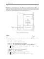
1
Master's Programme in Embedded and Intelligent Systems, 120 credits
MASTER THESIS
Architectural Design Space Exploration of
Heterogeneous Manycores
Benard Xypolitidis, Rudin Shabani
Master Thesis, 30 credits
Halmstad 2015-09-21
MASTER THESIS
Architectural Design Space Exploration of
Heterogeneous Manycores
School of Information Technology
Halmstad University
Benard Xypolitidis, Rudin Shabani
Supervisors: Zain-ul-Abdin, Ph.D.
Süleyman Savas
Halmstad, September 2015
Acknowledgements
We would like to thank our supervisors Dr. Zain Ul-Abdin and Süleyman Savas for their
time and effort. Their guidance throughout the thesis has been invaluable, which has
seen this project to its end. We would also like to thank professor Tomas Nordström
for suggesting and giving us the opportunity to work on this project. Last but not
least we would like to thank Satej Khandeparkar for his help and support during this
summer. Furthermore we would like to thank Halmstad University for providing us
with the faculties where the work has been carried out.
i
ii
Abstract
Exploring the benefits of heterogeneous architectures is becoming more desirable due
to migration from single core to manycore architectural systems. A fast way to explore
the heterogeneity is through an architectural design space exploration (ADSE) tool,
which gives the designer the option to explore design alternatives before the actual
implementation. Heracles Designer is an ADSE tool which allows the user to modify
large aspects of the architecture. At present, Heracles Designer is equipped with a
single type of processing core, a MIPS CPU.
We have extended the Heracles System in order to enable the system to model heterogeneity. Our system is called the Heterogeneous Heracles System (HHS), where a
different type of processing core, the OpenRISC CPU, is interfaced into the Heracles
System. Test programs are executed on both the MIPS and OpenRISC CPUs, which
have provided promising results. In order to provide the designer with the option to
modify the system architecture without changing the source code, a GUI named ADSET was created. ADSET provides the designer with the ability to modify the core
settings, memory system configuration and network topology configuration.
In the HHS the MIPS core can only execute basic instructions, while the OpenRISC
can execute more advanced instructions, giving a designer the option to explore the
effects of heterogeneity based on the big little architectural concept. The results of our
work provides an infrastructure on how to integrate different types of processing cores
into the HHS.
iii
Contents
1 Introduction
1.1 Aim . . . . . . . .
1.2 Problem Statement
1.3 Goals & Objectives
1.4 Approach . . . . .
1.5 Our contribution .
1.6 Work Outline . . .
.
.
.
.
.
.
.
.
.
.
.
.
.
.
.
.
.
.
.
.
.
.
.
.
.
.
.
.
.
.
.
.
.
.
.
.
.
.
.
.
.
.
.
.
.
.
.
.
.
.
.
.
.
.
.
.
.
.
.
.
.
.
.
.
.
.
.
.
.
.
.
.
.
.
.
.
.
.
.
.
.
.
.
.
.
.
.
.
.
.
.
.
.
.
.
.
.
.
.
.
.
.
.
.
.
.
.
.
3
4
4
4
4
5
5
2 Background
2.1 Heracles Designer . . . . . . . . . . . . .
2.1.1 Memory System Organization . .
2.1.2 Network Topology Configuration
2.2 OpenRISC . . . . . . . . . . . . . . . . .
2.2.1 Memory Addressing Modes . . .
2.3 Pipelining . . . . . . . . . . . . . . . . .
2.4 Software Toolchain . . . . . . . . . . . .
2.4.1 Executable and Linkable Format
2.4.2 .MEM files . . . . . . . . . . . . .
2.5 Heterogeneous Systems . . . . . . . . . .
2.6 Big Little Architectural Concept . . . . .
.
.
.
.
.
.
.
.
.
.
.
.
.
.
.
.
.
.
.
.
.
.
.
.
.
.
.
.
.
.
.
.
.
.
.
.
.
.
.
.
.
.
.
.
.
.
.
.
.
.
.
.
.
.
.
.
.
.
.
.
.
.
.
.
.
.
.
.
.
.
.
.
.
.
.
.
.
.
.
.
.
.
.
.
.
.
.
.
.
.
.
.
.
.
.
.
.
.
.
.
.
.
.
.
.
.
.
.
.
.
.
.
.
.
.
.
.
.
.
.
.
.
.
.
.
.
.
.
.
.
.
.
.
.
.
.
.
.
.
.
.
.
.
.
.
.
.
.
.
.
.
.
.
.
.
.
.
.
.
.
.
.
.
.
.
.
.
.
.
.
.
.
.
.
.
.
.
.
.
.
.
.
.
.
.
.
.
7
7
7
8
9
9
11
12
12
13
13
14
.
.
.
.
.
.
.
.
.
.
.
.
.
.
.
.
.
.
.
.
.
.
.
.
.
.
.
.
.
.
.
.
.
.
.
.
.
.
.
.
.
.
.
.
.
.
.
.
.
.
.
.
.
.
.
.
.
.
.
.
.
.
.
.
.
.
3 Related Work
17
4 Methodology
4.1 The Heracles System . . . . . . . . . .
4.1.1 From GUI to Raw Simulation .
4.1.2 Testing of the Heracles System
4.1.3 Architectural Overview . . . . .
4.2 Choice of CPU . . . . . . . . . . . . .
4.2.1 OpenRISC . . . . . . . . . . . .
4.2.2 IonMIPS . . . . . . . . . . . . .
4.3 OpenRISC . . . . . . . . . . . . . . . .
4.3.1 Hard-coded Testbench . . . . .
4.3.2 FPU . . . . . . . . . . . . . . .
4.3.3 Architectural Overview . . . . .
4.4 Tool Command Language Script . . . .
v
.
.
.
.
.
.
.
.
.
.
.
.
.
.
.
.
.
.
.
.
.
.
.
.
.
.
.
.
.
.
.
.
.
.
.
.
.
.
.
.
.
.
.
.
.
.
.
.
.
.
.
.
.
.
.
.
.
.
.
.
.
.
.
.
.
.
.
.
.
.
.
.
.
.
.
.
.
.
.
.
.
.
.
.
.
.
.
.
.
.
.
.
.
.
.
.
.
.
.
.
.
.
.
.
.
.
.
.
.
.
.
.
.
.
.
.
.
.
.
.
.
.
.
.
.
.
.
.
.
.
.
.
.
.
.
.
.
.
.
.
.
.
.
.
.
.
.
.
.
.
.
.
.
.
.
.
.
.
.
.
.
.
.
.
.
.
.
.
.
.
.
.
.
.
.
.
.
.
.
.
.
.
.
.
.
.
.
.
.
.
.
.
.
.
.
.
.
.
.
.
.
.
.
.
.
.
.
.
.
.
.
.
.
.
.
.
19
20
20
20
21
22
22
23
24
24
25
26
28
Contents
4.5
4.6
vi
Heterogeneous Heracles System . . . . . . . . . . . . .
4.5.1 Functionality of Heterogeneous Heracles System
4.5.2 Interfacer Module . . . . . . . . . . . . . . . . .
4.5.3 Testing . . . . . . . . . . . . . . . . . . . . . . .
GUI . . . . . . . . . . . . . . . . . . . . . . . . . . . .
5 Results
5.1 Heracles System . . . . . . . . . . . . .
5.1.1 Testing of the Heracles System
5.2 OpenRISC . . . . . . . . . . . . . . . .
5.2.1 Hard-coded Testbench . . . . .
5.2.2 FPU . . . . . . . . . . . . . . .
5.3 Heterogeneous Heracles System . . . .
5.3.1 Phase 1 . . . . . . . . . . . . .
5.3.2 Phase 2 . . . . . . . . . . . . .
.
.
.
.
.
.
.
.
.
.
.
.
.
.
.
.
.
.
.
.
.
.
.
.
.
.
.
.
.
.
.
.
.
.
.
.
.
.
.
.
.
.
.
.
.
.
.
.
.
.
.
.
.
.
.
.
.
.
.
.
.
.
.
.
.
.
.
.
.
.
.
.
.
.
.
.
.
.
.
.
.
.
.
.
.
.
.
.
.
.
.
.
.
.
.
.
.
.
.
.
.
.
.
.
.
.
.
.
.
.
.
.
.
.
.
.
.
28
29
30
32
33
.
.
.
.
.
.
.
.
.
.
.
.
.
.
.
.
.
.
.
.
.
.
.
.
.
.
.
.
.
.
.
.
.
.
.
.
.
.
.
.
.
.
.
.
.
.
.
.
.
.
.
.
.
.
.
.
.
.
.
.
.
.
.
.
.
.
.
.
.
.
.
.
37
37
37
38
38
39
40
40
41
6 Discussion
43
7 Conclusions
45
8 Future Work
47
Bibliography
49
List of Figures
2.1
2.2
2.3
2.4
2.5
2.6
2.7
Generic Heracles System Overview
Register Indirect with Displacement
Relative Addressing . . . . . . . . .
Classic RISC pipeline stages . . . .
Instruction pipeline stages . . . . .
Heterogeneous System . . . . . . .
big.LITTLE Architectural Concept
.
.
.
.
.
.
.
.
.
.
.
.
.
.
.
.
.
.
.
.
.
.
.
.
.
.
.
.
.
.
.
.
.
.
.
.
.
.
.
.
.
.
.
.
.
.
.
.
.
.
.
.
.
.
.
.
.
.
.
.
.
.
.
.
.
.
.
.
.
.
.
.
.
.
.
.
.
.
.
.
.
.
.
.
.
.
.
.
.
.
.
8
10
10
11
12
13
15
4.1
4.2
4.3
4.4
4.5
4.6
4.7
4.8
4.9
4.10
4.11
4.12
4.13
Generic System Overview . . . . . . . .
Parsing the .MEM files . . . . . . . . . .
Architectural Overview . . . . . . . . . .
l.lbz instruction . . . . . . . . . . . . . .
l.add instruction . . . . . . . . . . . . . .
OpenRISC FPU top module . . . . . . .
Floating point value . . . . . . . . . . .
OpenRISC System Overview . . . . . . .
The Heracles System file Hierarchy . . .
The Heracles System Program Flow . . .
Interfacer Module . . . . . . . . . . . . .
CPU communication with local memory
ADSET GUI window . . . . . . . . . . .
.
.
.
.
.
.
.
.
.
.
.
.
.
.
.
.
.
.
.
.
.
.
.
.
.
.
.
.
.
.
.
.
.
.
.
.
.
.
.
.
.
.
.
.
.
.
.
.
.
.
.
.
.
.
.
.
.
.
.
.
.
.
.
.
.
.
.
.
.
.
.
.
.
.
.
.
.
.
.
.
.
.
.
.
.
.
.
.
.
.
.
.
.
.
.
.
.
.
.
.
.
.
.
.
.
.
.
.
.
.
.
.
.
.
.
.
.
.
.
.
.
.
.
.
.
.
.
.
.
.
.
.
.
.
.
.
.
.
.
.
.
.
.
.
.
.
.
.
.
.
.
.
.
.
.
.
.
.
.
.
.
.
.
.
.
.
.
.
.
19
21
22
24
25
25
26
27
29
30
31
32
34
5.1
5.2
5.3
Waveform output of core0s test program . . . . . . . . . . . . . . . . .
OpenRISC Testbench . . . . . . . . . . . . . . . . . . . . . . . . . . . .
OpenRISC floating point test . . . . . . . . . . . . . . . . . . . . . . .
38
39
40
1
. . . . . . .
Addressing
. . . . . . .
. . . . . . .
. . . . . . .
. . . . . . .
. . . . . . .
.
.
.
.
.
.
.
.
.
.
.
.
.
.
.
.
.
.
.
.
.
.
.
.
.
.
.
.
.
.
.
.
.
.
.
.
.
.
.
.
.
.
.
.
.
.
.
.
.
.
.
.
List of Figures
2
1
Introduction
Processor architecture has gone through several changes in the 21st century, such as
internal design changes to the core architecture, communication protocol, amount of
peripheral units and the amount of cores per processor chip. Up until 2005, processor
designs usually had to operate at the highest frequency possible in order to achieve
high performance. However, increasing the frequency is not the solution to increase
the performance anymore due to power and temperature limits. Performance increase
solely by microarchitecture is measured by Pollack’s Rule. It states that performance
increase is roughly proportional to the square root of increase in complexity. This means
that if the logic in a processor is doubled, then it increases the performance by 40% [1].
Due to leakage current and the retardation in scaling the supply voltage, the number
of transistors will not increase as fast as it used to do. A solution to this problem is
the manycore processor architecture. By using several small cores on a processor chip,
each core might deliver lower performance compared to a bigger core, but the total
computational throughput of the system will be much higher. These systems are not
required to be symmetric or homogeneous. Multicore architectures were introduced
around 2005. These architectures have the potential to give a linear performance
improvement together with complexity and power. Two small cores instead of a large
monolithic processor core can achieve 70-80% higher performance [1]. The latest step
in processor architecture is the introduction of heterogeneity in manycore System on
Chip (SoC). An asymmetric (heterogeneous) SoC consists of large cores that handles
complex and heavy computations in combination with a large number of small cores
that execute less complex computations and using less energy. The heterogeneous SoCs
are even able to perform different types of computation, such as data streaming, and
digital signal processing by using special purpose cores. This gives the designer the
choice to either have an energy efficient architecture, used in portable devices, or have
a higher performance architecture and handle complex and heavy calculations.
When a new product is in development, the processor architecture needs to be heavily
modified or in some cases rebuilt. This cycle usually takes around two to three years.
With a design space exploration tool, the architecture can be modified according to
specific application requirements without going through the whole design cycle, which
reduces the development cost drastically.
3
1. Introduction
4
1.1 Aim
Heracles Designer is a architectural design space exploration (ADSE) tool, which gives
the designer the ability to explore different design alternatives. Some of the alternatives
which can be explored are: core settings, memory system configuration and on-chip
network configuration. The system is equipped with only a MIPS processing core. To
explore the heterogeneity of the Heracles System a second processing core type needs
to be incorporated. The aim of this project is to extend the Heracles System in such
a way that it incorporates a new type of processing core.
1.2 Problem Statement
Three major problems have been assessed. First and foremost, can the Heracles System
be extended to incorporate a new type of processing core? If so, how much of the system
needs to be modified? Secondly, is the new processing core compatible and can it be
incorporated inside the Heracles System? How much does the processing core need to
be modified in order for it to be interfaced into the Heracles System? Lastly, upon
achieving the integration of the new processing core, will both cores be able to run
simultaneously?
1.3 Goals & Objectives
Our objective is to have a system that can model the heterogeneity. An architectural
design space exploration tool, Heracles Designer, is chosen for this purpose. Thus, our
main goal for this project is to enable the heterogeneity for the Heracles System. Besides exploring the heterogeneity on a core level, further exploring the heterogeneity by
choosing different interconnecting networks is desired. By modifying the architecture
of the CPU, e.g. adding a new instruction, different tests can be run to observe the
benefits and bottlenecks of reconfiguring the heterogeneity. To make it easier for the
designer to reconfigure the system architecture, a GUI will be created which gives the
option to modify the core settings, memory system configuration and network topology
configuration. By introducing heterogeneity into a system, a better energy efficiency
might be achieved. Thus, a correlation between energy efficiency and computational
power can be explored.
1.4 Approach
Our approach is to begin exploring the architectural design space exploration tool
called Heracles Designer. This will be followed up by studying different processing
cores in order to select the appropriate core to be integrated into the Heracles System.
Testing on the Heracles System will be done by writing a C test program for the MIPS
cores. The test program will be compiled and be submitted to the MIPS software
1. Introduction
5
toolchain. This will generate the corresponding .MEM files, which hold the processors
machine code, which is then loaded into the local memory of each MIPS processing
core. Upon selecting the appropriate processing core, tests will be executed to ensure
the functionality of it. Interfacing the processing core inside the Heracles System will
be achieved by creating a new module that will work as a bridge between the new
processing core and the system. In this module the various input/output (I/O) ports
of the new processing core will be mapped to I/O of the Heracles System. Furthermore,
a address translation logic will be put in place so that the correct addresses are mapped
from the integrated core to the Heracles System. Some of the integrated cores signals
on the various modules might have to be modified. Test are then done to evaluate the
new systems functionality. These tests will be executed on all the processing cores.
1.5 Our contribution
We have achieved to extend the Heracles System to incorporate a new processing core.
The integrated processing core is the OpenRISC CPU. The new system is dubbed the
Heterogeneous Heracles System (HHS). Tests have been executed on all the processing
cores. The MIPS processing cores can execute basic operations while the OpenRISC
can execute more advanced operations. The HHS gives the designer the option to
explore heterogeneity on different system architectures. For the designer to modify
the system architecture without having to change variables in the source code, we have
created a GUI called ADSET. With this GUI the designer can change the core settings,
memory system configuration and network topology.
1.6 Work Outline
The Background chapter will describe some of the key concepts this thesis will touch in
more detail. In Related Works, a literature review will be conducted between similar
projects and our thesis. The Methodology chapter will divulge how this thesis has
been accomplished. In the Results chapter, the extended Heracles System is tested
and the results are shown, which will be followed by Discussion. The thesis will end
with Conclusion and Future Work.
1. Introduction
6
2
Background
This chapter will describe various key concept that are important to understand in
order to grasp the full project. Background information about the Heracles System
and the integrated OpenRISC processing core is also provided in this chapter.
2.1 Heracles Designer
Heracles Designer is an open-source architectural design space exploration (ADSE)
tool, which can be configured into different topologies, routing schemes, processing elements or cores and memory system organizations. In order to support fast exploration
of future manycore architectures, the Heracles System is constructed with a high degree of modularity. The main purpose of this platform is for architectural exploration
in research and teaching environments [2]. Options given to the designer by Heracles
Designer are to reconfigure and synthesize different systems based on an integer 7-stage
pipelined MIPS core. The MIPS cores available are either single- or twothreaded. The
programming language Verilog, which is a Hardware Description Language (HDL), is
used to construct each module [3, 4]. Heracles Designer has the option to port the
synthesized architecture to an Field Programmable Gate Array (FPGA) [5]. A FPGA
is an integrated circuit that contains logic blocks which can be configured and interconnected to the designers configuration.
A generic overview of the overall structure of the Heracles System is depicted in Figure 2.1.
2.1.1 Memory System Organization
Heracles Designer provides several ways of configuring the memory topology of a processor. The memory system is parameterized and can be configured independent from
the rest of the system. It consist of three key components, namely:
• The cache system: composed of 1-level cache with a direct-mapped instruction
cache and data cache. This can be extended to more cache levels. Each of the
caches can be configured independently.
7
2. Background
8
Figure 2.1: Generic Heracles System Overview
• The local memory distribution: constructed to allow different memory space
configurations. Its key attribute is that the size can be changed on each individual
core.
• The network interface: has an address resolution logic which works with a Packetizer module in order to get the caches and local memory to communicate with
the rest of the system. The data traffic goes through the address resolution logic
in order to determine if a request can be served at the local memory or if it has
to be sent over the network [6].
2.1.2 Network Topology Configuration
The router architecture used in the Heracles System is an implementation of a Network
on Chip (NoC) in order to make it scalable. This NoC architecture is defined by its
topology, its own mechanism and its routing algorithm. The key features used for the
definition of the router architecture are: [7]
•
•
•
•
RC- used for routing.
VA- used for virtual allocation.
SA- used for switch allocation.
ST- used for switch traversal.
The route computation and virtual channel allocation are implemented by using algorithms which compute the routes in the NoC architectures. These algorithms are
categorized as oblivious and dynamic. Heracles Designer supports oblivious routing algorithms using some fixed logic or a routing table. The network topology configuration
2. Background
9
uses the parameterization of the number of input and output ports on the router and
the table-based routing to provide the Heracles System with flexibility and the capability to support different network topologies. The topologies than can be implemented
are: k-array, n-cube, 2D-mesh, 3D-mesh, hypercube, ring and tree.
2.2 OpenRISC
The OpenRISC, which this thesis studies, consists of a power management unit, debug unit, tick timer, programmable interrupt controller (PIC), central processing unit
(CPU), and memory management hardware [8]. The OpenRISC CPU is based on a
5-stage pipelined RISC architecture. By using the standardized 32-bit Whisbone bus
interface, peripheral system and a memory subsystem may be added. The OpenRISC
is intended to have a performance comparable to an ARM10 processor architecture.
Furthermore, OpenRISC is a 32- and 64-bit processor which supports floating point as
well as vector processing [9]. The OpenRISC system architecture is still an ongoing
project.
2.2.1 Memory Addressing Modes
An effective address is computed by the processor upon a memory access instruction
execution, branch instruction execution or when fetching the next sequential instruction. If the maximum effective address in logical address space is exceeded due to
the sum of the operand length and the effective address, the memory operand wraps
around from the maximum effective address through effective address zero.
Register Indirect with Displacement
Instructions using this addressing mode contain a signed 16-bit immediate value. The
immediate value is sign-extended and summed with the contents of the general-purpose
register (GPR) specified in the instruction, which will result in the effective address [10].
Figure 2.2 shows the register indirect with displacement addressing mode computing
the effective address. Instructions that use this mode are load/store instructions.
2. Background
10
Figure 2.2: Register Indirect with Displacement Addressing
PC Relative
Instructions using the addressing mode ”PC Relative” contain a signed 26-bit immediate value. The immediate value is sign-extended and summed with the contents of
Program Counter (PC) register [10]. Figure 2.3 shows the PC relative addressing
mode generating the effective address. Instructions that use this mode are branch
instructions.
Figure 2.3: Relative Addressing
2. Background
11
2.3 Pipelining
Pipelining is a technique used when designing a processor in order to increase the
instruction throughput i.e. the number of instructions executed per time unit. This
is done by dividing the instruction cycle into a series, called pipeline. This increases
the instruction throughput by performing multiple operations concurrently, while not
reducing the latency considerably. Figure 2.4 shows how a standard pipelining structure might look like. The number of stages in the pipeline differs depending on which
architecture is used, though the most common is the classic RISC pipeline [11].
Figure 2.5 illustrates an instruction pipeline. The coloured boxes represent different
instructions. To show how the pipelining concept works, a number of 9 clock-cycles
(clks) were chosen. In clk 0 we have four instructions waiting to be executed. At clk
1 the green instruction is fetched from the memory. Moving on to clk 2, the green
instruction is decoded and the purple instruction is fetched from the memory. Now
at clk 3 the green instruction is executed, which means that an actual operation is
performed, then the purple instruction is decoded and the blue instruction is fetched.
At clk 4 the green instruction’s results are written back to the register file or to the
memory, the purple instruction is executed, the blue is decoded and the red is fetched.
At clk 5 the green instruction is completed, the purple is written back, the blue is
executed and the red is decoded. Then at clk 6 the purple instruction is completed,
the blue is written back and the red is executed. Two instructions are left and at
clk 7 the blue is completed and the red is written back. At clk 8 all instructions are
completed.
Figure 2.4: Classic RISC pipeline stages
2. Background
12
Figure 2.5: Instruction pipeline stages
2.4 Software Toolchain
The Heracles System has an open-source software toolchain based on the orignal GCC
MIPS corss-compiler. A software toolchain provides a set of tools in order to run
standard C code on a specific architecture. This is accomplished by running the C
program through a compiler, which produces an assembly file. The assembly file is
run through an assembler which creates object files of the assembly code. Finally, the
object files are linked together through a linker script which produce the binary files
contating the machine code with the instructions of the specific processor architecture.
Each processor architecture requires their own unique software toolchain. Commonly
for the processor cores the software toolchain produces a file called Executable and
Linkable Format (.ELF). The MIPS processing core used in the Heracles System does
not fully support all of the instructions used in the original MIPS R3000 series [12]. For
this reason the Heracles System uses memory dump files called .MEM files (explained
in section 2.4.2).
2.4.1 Executable and Linkable Format
The Heracles software toolchain produces .MEM files, which are memory dump files
containing the machine code for the processor. Software toolchains usually produce
Executable and Linkable Format (.ELF) files. .ELF is a file type that is used both in
2. Background
13
computer programs and embedded programs and acts as a translator between programming language and architecture specific machine code. .ELF files are object files that
are produced by the compiler and the linker. These files are binary representations of
a program intended to be executed on a specific processor architecture. In order to be
understood in a machine independent way, the standard format of .ELF files include
a header file [13]. During the Choice of CPU study, .ELF files were used to test and
verify the IonMIPS processor (see 4.2.2).
2.4.2 .MEM files
The MIPS core implemented in the Heracles System does not support all the instructions that are present in the MIPS-I instruction set architecture (ISA), thus the standard MIPS software toolchain is not used. This has been solved by using parts of
the official MIPS/GNU toolchain together with an instruction set architecture checker
called isa-checker. The isa-checker goes through the code and checks if there are any
exceptions regarding the instructions that can be carried out by the processor. If the
program passes this check then it generates two files for each processing core, a .MEM
file and a .TXT file. The architecture specific machine code is located in the .MEM
file while the .TXT file contains declarations about the program starting address, main
function address and the size of the stack frame.
2.5 Heterogeneous Systems
The term Heterogeneous Computing means that a computing system uses more than
one type of processing core. This concept was implemented to fully exploit the benefits
and capabilities of multiple parallel execution units. In order to achieve heterogeneity,
the computer system needs to integrate different types of computational elements on a
single platform [14]. An example of such a platform is a System on Chip (SoC), which
incorporates a Central Processing Unit (CPU), a Radio Processing Unit (RPU) and a
Graphics and Video Processing Units (GPU+VPU), and all units share the same data
buses and memory (see Figure 2.6).
Figure 2.6: Heterogeneous System
2. Background
14
This concept introduces heterogeneity into the system architecture. The main criteria
for a system to be considered heterogeneous is for the system to be equipped with at
least two types of processing cores which have different Instruction Set Architecture
(ISA) [15]. ISA is the architectural functionality of the processing core, which can
consist of: the addressing model it uses, the type of instructions that can be executed,
the amount of registers it contains etc. Heterogeneous Computing can also be extended
to incorporate processing cores of the same ISA but with different microarchitectures.
The microarchitecture is the way an ISA is implemented in a particular processing
core. An example of the mentioned exception above is ARMs big.LITTLE architecture,
where the ISAs of the big and LITTLE cores are the same and the term heterogeneity
refers to the speed of the different microarchitectures [16].
2.6 Big Little Architectural Concept
The developed Heterogeneous Heracles System (HHS) is composed of two different
types of CPUs, the MIPS and the OpenRISC. The MIPS processing core can execute less complex computations, while the OpenRISC can execute complex heavy
computations. The functionality of the HHS resembles ARMs big.LITTLE architectural concept. ARMs big.LITTLE system is a heterogeneous computing architecture
which combines two kinds of processing cores on the same System On Chip (SoC). The
big.LITTLE consists of a slower, low-power processing core (cortex-A7 or Cortex-A53)
and a more powerful and power-consuming processing core (Cortex-A15 or CortexA57). Depending on the task at hand, the appropriate processing core is selected, with
the option to select multiple processors. Figure 2.7 shows an architectural concept
of the big.LITTLE during low load and during high load in a single processor. The
selection of the cores works seamlessly and the processors appear identical from an
applications software perspective. The approach of choosing the appropriate processor
for the task at hand, enables highly optimized processing, which results in significant
energy savings for common workloads [17]. This is a great solution to one of today’s
great problems, which is to offer high-performance and extended battery life. This is
the main focus of the big.LITTLE architectural concept, to allow devices to select the
right processor for the right task, based on performance requirements.
2. Background
15
Figure 2.7: big.LITTLE Architectural Concept
2. Background
16
3
Related Work
In this chapter a literature review is performed on works related to our topic. Four
scientific papers are reviewed and a comparison is made to our work. Furthermore, the
differences are discussed and how our project can benefit from the already achieved
work.
Cores in multicore platforms use communication resources simultaneously which causes
an increase in the bandwidth demand. Ordinary shared bus system do not scale, thus
the need to use Network on Chip (NoC) architecture. NoC solves the scalability issue
by complimenting the topology design, together with an on-chip interconnect system
in the form of packet-based communication. J. Öberg et al. [18] have developed a
NoC generator which can generate 1D, 2D or 3D Mesh and Torus topologies. Through
an XML configuration file the NoC generator generates an arbitrarily large multicore
platform. The tool builds up the manycore system based on HDL files written in
VHDL. The system is then exported onto an Field Programmable Gate Array (FPGA)
where the capabilities of the NoC are tested by writing a C program for the processing
cores to exchange data, thus creating network traffic in the System on Chip (SoC)
FPGA.
The NoC generator, in loose terms, is an exploration tool in which a designer can set
up different types of NoC topology. The Heterogeneous Heracles System (HHS) also
has the capability to generate various Network topologies, although not to the extent J.
Öberg et al. [18] have achieved. What HHS excels on is the ability to explore different
types of processor architecture by allowing the user to modify a vast amount of aspects
to the structure of the system. This ranges from the memory to the NoC and cache
scalability.
A scalable manycore processor architecture with OpenRISC as a processing element is
proposed by H. Chien et al. [19]. The processing cores are connected via a mesh-based
NoC and has access to an external memory. They propose a XY routing to avoid any
deadlock on routing paths. Each OpenRISC processor has a local memory, a communication unit and a DMA engine. The framework developed is intended for analysis,
verification and validation of manycore processor architecture for embedded parallel
applications. This can be done in different abstraction levels: Electronic System Level
(ESL), Register Transfer Level (RTL), gate-level and FPGA physical platforms.
In our thesis we only look at the RTL level of abstraction. The architecture presented on
17
3. Related Work
18
this paper can only scale the processor architecture. The HHS that has been developed
is a design space exploration tool. This means that, besides scaling the architecture,
various configurations can be made to the system and thus the heterogeneity can be
explored.
N. Genko et al. [20] have created an emulation framework, which is implemented in an
FPGA. This enables exploration, verification and comparison of a wide area of NoC
topologies. The emulation framework has been designed with modularity in mind. It
only uses one hard coded processing core, since the main research is to emulate NoC
topologies. The emulation framework is a NoC programmable platform. It consists
of Traffic Generators, Traffic Receptors and user defined interconnections between the
switches of the network.
The differences between this and our thesis is that they only explore network topologies
and different NoC configurations. The processing cores are hard-coded and there is only
one to choose from. In other words you can only explore the design space architectural
changes in the network and not in the whole system architecture, which can be achieved
with HHS.
A design space exploration tool is presented by Lahiri K. et al. [21]. This design
space exploration tool is used for optimization of system-level on-chip communication
architectures. The tool consists of two algorithms. The first algorithm is a clustering
algorithm for mapping the SoC communications to network and topology. The second
algorithm is an iterative algorithm that dynamically improves the previous algorithm.
Our project extends a architectural design space exploration (ADSE) tool where the
main focus lies in exploring architectural changes in a processor core of a SoC, while
Lahiri K. et al., focuses on the communication of a whole SoC system. Implementing
the two algorithms stated above in the SoC systems, the authors try to automate
the design process. The automated system has shown to perform better than any
conventional communication architectures.
4
Methodology
This chapter will explain in depth how each step was taken to reach the final goal, which
is to extend the Heracles System to incorporate a new type of processing core. Different
processors were studied to find the most suitable type of processor for integration.
Furthermore, tests were executed on the Heracles System and the OpenRISC processing
core. OpenRISC is the chosen CPU to be interfaced into the Heracles System. These
test are done to evaluate both the Heracles System and the OpenRISC CPU, and
inherently gain the understanding of each architectural structure so that the interfacing
can begin. Figure 4.1 depicts a node in the Heracles System. The final result will scale
the number of nodes to a designers specifications with the CPU being either a MIPS
or OpenRISC processing core.
Figure 4.1: Generic System Overview
19
4. Methodology
20
4.1 The Heracles System
The verilog files, where every module together composes the structure of the Heracles
System, were studied intently to understand the flow of the system. Furthermore, how
the files are generated from the Heracles Systems GUI were as well looked at.
4.1.1 From GUI to Raw Simulation
The Heracles System includes a Graphical User Interface (GUI), which is called Heracles Designer, where different options can be set in order to generate the desired
architecture. When all the options are set, Heracles Designer saves a module named
real cores mesh wrapper, where the designer inputs are declared. The designers options are then to either simulate the architecture through ModelSim or export it to
an FPGA. Heracles Designer generates a testbench which is run through a TCL script
(see section 4.4). The testbench runs the system where real cores mesh is set as the
top module.
In order to modify the Heracles System, the verilog files were extracted from the installed directory and put into a separate folder. The verilog files contain all the necessary modules, along with the generated testbench. The TCL script was modified in
order to run from the new folder. After the modifications the architecture could be run
directly from ModelSim, without going through Heracles Designer. The modules were
also added to Xilinx IDE, which provided the Register Transfer Level (RTL) schematic
of the system. The RTL schematic depicts the modules and all the interconnected
input/output signals.
4.1.2 Testing of the Heracles System
Upon extracting all the modules from Heracles Designer, a new system set-up was
instantiated and run through ModelSim. This set-up contained all the verilog files,
composing the Heracles System. At this stage a basic test program was implemented.
The main purpose of this test program was to see how the pipelining stages are handled upon using multiple processing cores in the Heracles System. A setup with four
processing cores was dimensioned. The test program was written in C and compiled
with Heracles software toolchain, which produced a .MEM file for each core. Two cores
performed addition with a set of integer values. The remaining two cores performed
subtraction with the same set of integer values. The .MEM files are loaded into the
Heracles Designer as is shown in Figure 4.2.
4. Methodology
21
Figure 4.2: Parsing the .MEM files
After loading the .MEM files into Heracles Designer the real cores mesh wrapper verilog
file is generated. In real cores mesh wrapper the starting address for each core is set,
which is accessed by the program counter. The .MEM files are automatically loaded
into each core’s local memory through a TCL script (see section 4.4). The Heracles
System is then simulated through ModelSim. The results are shown on chapter 5.1.
4.1.3 Architectural Overview
After executing the test program and going in more depth on the Heracles Sytem
modules, an understanding of the architectural structure of the system was obtained.
Figure 4.3 depicts the module hierarchy of the Heracles System.
Below follows a description of some of the more important modules:
• Real Cores Mesh: Is responsible for scaling the number of processing cores.
The cores are interconnected through the Network on Chip (NoC).
• Memory Router System: Is responsible for the interaction with the MIPS
CPU. Furthermore, the module communicates with the NoC through the incoming and out-going packets.
• Memory System Wrapper: Is responsible for the instruction/data cache and
the local memory which is interfaced with the CPU.
• Router Wrapper: The NoC functionalities are handled in this module. The
module uses the router and the network interface, which communicates with the
CPU and the network.
• 7-stage-MIPS: Is responsible for all the seven stages of the pipelining. The
memory router system module is called from this verilog file.
• Direct Mapped Cache: Contains the instruction and data cache, which are
numbered for each CPU.
4. Methodology
22
• Local Memory: Contains the local memory for each generated CPU.
• ALU: Is responsible for all the arithmetic operations.
Figure 4.3: Architectural Overview
4.2 Choice of CPU
The processor provided by the Heracles System is a simple variation of a MIPS processor which does not support important operations such as: multiplication, division,
floating point operations etc. For this reason different processors where evaluated.
After several processor evaluations the choice was between IonMIPS [22] and OpenRISC [23]. This chapter discusses the strength/weakness of both architectures in order
to motivate the selection of the appropriate processor for this project.
4.2.1 OpenRISC
The source code for OpenRISC provided by OpenCores is for a complete System on
Chip (SoC) architecture. The implementation of the SoC with OpenRISC processing
core has the following specifications:
• 32 bit address
• 32 bit data bus
• 32 registers which can hold 32 bits of data each
4. Methodology
•
•
•
•
•
23
ALU which supports ADD, SUB, MUL, DIV
Floating Point Unit, Multiply And Accumulate (MAC) unit
Built in exception handler
Special purpose registers
Debug module
The OpenRISC processing core has similar specifications as the MIPS CPU used in the
Heracles System. The ALU supports MUL and DIV arithmetic operations, something
that the MIPS CPU does not support. Furthermore, it also has a support for floating
point operations. OpenRISC is equipped with various useful modules such as debug
unit, Multiply And Accumulate (MAC) unit, which could later on be added into the
Heracles System in order to make it more powerful.
4.2.2 IonMIPS
IonMIPS is a architectural system where the designed CPU is MIPS-I compatible [24].
The IonMIPS consists of the following key features:
•
•
•
•
Binary compatible to R3000 series of CPUs.
Kernel/user mode operation as per the architecture definition.
Exception handling compatible to MIPS-I standard.
Includes minimalistic memory handler with interfaces for external SRAM (or
FLASH) on 8- and 16-bit data bus.
• Size and speed comparable to other free MIPS cores.
Testing of IonMIPS
In order to test the IonMIPS processor a software toolchain was generated through
Sourcery Codebench Lite [25]. The processor was then verified by running a simple
hello world program. The test program was written in C, which was compiled with
the generated software toolchain. The software toolchain generated a .ELF file, which
was used to execute the test program on the processor.
Conclusion
Most of the IonMIPS features are hard-coded to fit specific FPGAs. The IonMIPS
project is still in an early development stage. Thus, it lacks some important key features
such as: real documentation (specifications or datasheet), hardware interrupts etc.
The IonMIPS CPU does not have a fully implemented CPU memory communication
interface. IonMIPS has an 8-bit bus, while OpenRISC has a 32-bit bus and the Heracles
4. Methodology
24
memory system also has a 32-bit data/address bus. Therefore it was easier to seamlessly
integrate the OpenRISC with the Heracles System instead of the IonMIPS.
4.3 OpenRISC
Upon electing the new type of processing core for integration into the Heracles System,
tests were executed in order to verify that the functionality of the core worked as
intended. Tests are performed on the OpenRISC in its original form, without any
modifications from us.
4.3.1 Hard-coded Testbench
In order to see the general behaviour of the OpenRISC, a broad overview of the architecture was depicted. This was achieved by porting all the verilog files into Xilinx
IDE. There the files are checked for syntax errors before the architecture can be synthesized. The IDE in turn creates an Register Level Transfer (RTL) schematic over
the whole architecture. The RTL schematic depicts the modules and all the interconnected input/output signals. A module that replicates the inputs and outputs of the
or1200 cpu module is created. The signals are defined and initialized before they are
connected to the actual or1200 cpu module. In order to test the OpenRISC architecture, three instructions are executed. Each of the first two instructions load an integer
value to a predefined register. The third instruction adds the two values and saves the
result in the appropriate register. The signal “icpu dat i” in the or1200 cpu module
is responsible for the 32-bit instruction. The signal receives the instruction at positive
clock edge and then forwards the 6 most significant bits (msb) to the instruction fetch
module. The signal “icpu ack i” is the acknowledgement signal given by the memory
to communicate to the or1200 cpu module that the instruction has been fetched by
the instruction fetch module and to start with the decoding stage. The data is passed
into the signal “dcpu dat i ” at positive clock edge, which is followed by toggling the
“icpu ack i” signal. These steps are repeated for every instruction being passed.
The load instruction “Load Byte and Extend with Zero” can be seen in figure 4.4.
Figure 4.4: l.lbz instruction
The contents of general-purpose register “A” is added with the sign-extended offset
value. The sum is the effective address, which is the location of an operand of the
4. Methodology
25
instruction. The eight least significant bits (lsb) of the byte in memory addressed by
“A” are loaded into the eight lsb of the general-purpose register “D”. The rest of the
bits in general-purpose register “D” are replaced by zeros.
The add instruction can be seen in figure 4.5.
Figure 4.5: l.add instruction
The contents of both general-purpose register “A” and “B” are added together. The
result of the addition is placed into the general-purpose register “D”.
4.3.2 FPU
The MIPS core that is used during this project does not support any floating point
operations. However, OpenRISC is constructed with the modules required to execute
floating point operations. To fully grasp how this has been implemented, a module was
created to test and verify the Floating Point Unit (FPU).
Figure 4.6: OpenRISC FPU top module
The created module declares and initializes the appropriate signals, which are then
linked to the signals of the top module of the FPU (see figure 4.6). This is done to
circumvent the need to initialize the whole architecture and avoid any pitfalls that
might arise. The point of this testbench is to only verify the FPU, and the created
module simulates the signals as if they are being sent from the CPU. After the signals
are initialized, two values are passed into two variables, “a” and “b”, which are followed
by the opcode for the specific FPU operation. The opcode is passed into the variable
“f pu op”. Before the values to “a” and “b” are passed, the signal “ex f reeze” is
4. Methodology
26
set to one. This signal is reverted back to zero after the opcode is passed. Without
toggling this signal the FPU module will not execute the operation. First two whole
integer values are added to clearly see the result. When the result has been verified,
two floating point units are added. The floating point values are given in the IEE754
Single Precision binary floating point binary32 format shown in figure 4.7.
Figure 4.7: Floating point value
The exponent needs to represent both positive and negative exponents. This is managed by using a biased exponent, which is composed by adding the original exponent
with a constant bias. For 32-bit floating point the constant bias is 127. The result
from adding two floating point values will be depicted in the same format as depicted
in figure 4.7.
4.3.3 Architectural Overview
While testing and verifying the OpenRISC through the hardcoded testbenches we
studied the modules in more depth. After executing these tests, an understanding of
the architectural structure of OpenRISC was obtained. Figure 4.8 depicts the module
hierarchy of the OpenRISC System. Figure 4.8 describes the module hierarchy for
the complete System on Chip (SoC) implementation using the OpenRISC processing
core. It is to be noted that only the CPU with its sub-modules were integrated into
the Heracles System. The OpenRISC CPU will be interfaced to use the peripherals
provided in the Heracles System, instead of using its default SoC peripherals. Below
follows a description of the more important modules of OpenRISC:
• CPU: Connects all the instantiation of the internal CPU modules.
• PC: This module works as a program counter and is interfaced to the Instruction
Cache of the processor.
• Instruction Fetch: This module takes care of the instruction fetch stage of the
pipelining and interfaces to the Instruction Cache.
• Configuration Registers: The majority of the instruction decoding is performed in this module.
• Load/Store unit: Is responsible for load and store operations, interfaces between the Data Cache and the CPU.
• ALU: Is responsible for all the arithmetic operations.
• FPU: Contains all the FPU arithmetic operations, wrapper for floating point
unit, interface based on Multiply and Accumulate (MAC) unit.
4. Methodology
27
Figure 4.8: OpenRISC System Overview
• SPRs: Is responsible for the decoding of the Special Purpose Register addresses
and their access to the Special Purpose Registers. The OpenRISC uses these
special purpose registers to communicate with its peripherals.
Another important module, which is not present at figure 4.8 is the or1200 defines
module. This module contains a list of predefined variables used throughout the system.
4. Methodology
28
4.4 Tool Command Language Script
A Tool Command Language (TCL) script is used as a setup for the simulation. A
compilation check is done for all the design files included inside the TCL script. It
then starts the testbench which uses the output file from the Heracles Designer. The
caches are initialized for all the cores and set to zero. The TCL script does the most
important job of loading the .TXT files, which contain the machine code program for
each processor, into the local memories of all the cores.
The TCL script starts with a libary list which has all the design files of Heracles
System and the OpenRISC CPU, which are checked if they are compiled or not. It
then sets up the testbench to start the simulation which uses the output file from the
Heracles Designer. The number of cores used in the Heterogeneous Heracles System
(HHS) are set by a variable that generates the total number of processing cores present
in the system. This variable is always even, where half the cores are represented by
OpenRISC, and the other half is represented by MIPS processing cores. The files to be
loaded in the local memories of the MIPS respectively the OpenRISC processing cores
are specified with their complete path and corresponding core value to the location
they will be loaded. To load the program into a specific local memory or to initialize a
cache, the complete path needs to be specified. This complete path is broken down into
the common path, core number and the rest of the path into the local memory or cache.
The common path is set in the variable “top part”. The instruction and data cache are
denoted by “icache” and “dcache” respectively, which are the cache paths for the MIPS
CPU. The cache paths for the OpenRISC CPU are denoted as “icahce OpenRISC ” and
“dcache OpenRISC ”. The script then initializes the caches of the MIPS and OpenRISC
to contain zeroes. The path to local memory of the MIPS CPU and OpenRISC CPU
is set in the variable “mem part” and “mem part risc” respectively. It then loads the
.TXT files for both the CPUs in their respective local memories. Towards the end of
the script the waveforms are loaded and the total simulation time is recorded.
4.5 Heterogeneous Heracles System
Upon fully integrating the OpenRISC processing core into the Heracles System, a
new system was created. We have elected to name this new system the Heterogeneous
Heracles System (HHS). The HHS fully maintains the original properties of the Heracles
system, such as scaling the number of processing cores and dimensioning both the
memory and network topologies. For the evaluation of the HHS functionality, test are
performed on all the processing cores present in the system. The system generated
for evaluation contained four MIPS and four OpenRISC processing cores. Figure 4.9
shows the hierarchy of the verilog modules in the Heracles System.
4. Methodology
29
Figure 4.9: The Heracles System file Hierarchy
The modules with the highest file hierarchy and consequently the most important are:
• Real Cores Mesh: This module is responsible for instantiating the specific
number of cores and interconnecting them through the NoC.
• Processing Cores: MIPS or OpenRISC CPU.
• Memory Subsystem & and Router: This module interacts with the core.
The instruction flow inside the Heracles System is described in Figure 4.10.
4.5.1 Functionality of Heterogeneous Heracles System
• After the inputs are entered in ADSET (see Section 4.6), a verilog output file is
generated which has all the parameters initialized to corresponding input values.
Furthermore, the verilog files have the starting addresses of all the local memories
interfaced to every cpu.
• The generated file from ADSET instantiates the real cores mesh module. The real
cores mesh module instantiates the MIPS and the OpenRISC core. The real cores
mesh is modified to achieve the desired scalability. Thus if the Heterogeneous
Heracles System (HHS) has 8 cores in total then the architecture has four MIPS
and four OpenRISC cores.
4. Methodology
30
• Every node (see Figures 4.1, 4.3) in the Heterogeneous Heracles System (HHS)
consists of either a MIPS or a OpenRISC core which instantiate the module
memory router system. The memory router system is responsible for the caches,
local memories, and the packetizer modules. It is also responsible for the Network
on Chip (NoC) communication between the modules.
• The real cores mesh forwards a starting address for each processing core in the
system, which are provided by the generated verilog file from Heracles Designer.
It uses this starting address to communicate with the caches and thus executes
the program loaded into the local memory by the TCL script.
• When a Core wants to send data to another core in the system it first sends the
data into the Memory. Once the Memory has received the data from the Core
it then transfers the data to the Packetizer. In the Packetizer the data is split
and put into data packets and then sent on to the Network Interface which in
turn sends the data packets over to the Router. The Router will route the data
to the correct address it needs to be sent to and then sends the packets over to
the Network on Chip.
• For the Core that is receiving the data the program flow is reversed. The Router
receives the data packets from the Network on Chip and sends them over to the
Network Interface. The Network Interface will then forward the data packets to
the Packetizer. In the Packetizer the data packages will now be converted back
to their original data format and send it to the Memory. The Core will then
access the Memory and retrieve the data.
Figure 4.10: The Heracles System Program Flow
4.5.2 Interfacer Module
The interfacer module (see Figure 4.11) was developed to instantiate the OpenRISC
CPU and memory router system. This is done in a similar fashion to the original design
of the MIPS core so that a modular design can be kept. The interfacer module could
then be instantiated by the real cores mesh module to achieve heterogeneity.
The OpenRISC CPU communicates with the memory router system using the address
translation logic (see Figure 4.11) for the instruction and data address. The address
4. Methodology
31
translation is an important part of the HHS as it concatenates the processing core
number, generated by the Heracles System, with the address generated by the OpenRISC CPU. The new address is then sent to the memory router system which utilizes
the address to find the instruction at that particular address.
Figure 4.11: Interfacer Module
Signals
The signals below are used to create the interface between the or1200 cpu and the
memory router system:
•
•
•
•
•
•
•
•
•
•
•
clk : The clock signal for the CPU
rst: The reset signal to initialize the CPU
fetch : To fetch the instruction from the memory
icpu adr o : The address from the OpenRISC to fetch the instruction
icpu dat i : The instruction from the memory for the OpenRISC to execute
icpu ack i : Acknowledgement signal from the memory to signal the OpenRISC
that the transfer is over
data f etch: To fetch the data from the memory
dcpu we o : To write to the memory
dcpu adr o: Address to fetch the data from the memory
dcpu dat i : The data placed on the databus
dcpu ack i : Acknowledgement that the databus transfer is done
4. Methodology
32
OpenRISC Modifications
The program address is the starting address which the Program Counter (PC) points
during startup. This is given by the real cores mesh module to the MIPS, and within
MIPS, this program address is assigned to the PC at reset. A similar approach has to
be followed to integrate the OpenRISC into the Heracles System. This was achieved by
passing the program address from the real cores mesh module to the interfacer module.
The interfacer module accepted it as an input and passes it to the OpenRISC CPU
core. The OpenRISC CPU core has a module, or1200 genpc, which is responsible for
updating the PC as the instructions are decoded. This program address had to be
assigned to the PC at reset. The challenge here was, after this part was accomplished,
OpenRISC was not incrementing the PC. It was fixed by changing the part in the
or1200 genpc module which is responsible for updating the PC. Thus the or1200 genpc
module of the OpenRISC was modified to give the starting address of the Heracles
System to the PC of the OpenRISC. The fetch signal was added to the same module
which tells the memory router system that an address is available on the “i address”
port. The load store module named “or1200 lsu” of the OpenRISC was modified to
add the “data f etch” signal.
4.5.3 Testing
In order to verify the complete Heterogeneous Heracles System (HHS), various programs were executed, which confirmed that the integrated signals and the modifications
described above worked as intended.
Figure 4.12: CPU communication with local memory
4. Methodology
33
Figure 4.12 depicts how the CPU communicates with the local memory through caches
and how the TCL script loads the test program into the memory.
Phase 1
In this phase, a program which contained 99 NOPs and one ADDI instruction to store
an immediate value in register 3 was executed. The NOPs and ADDI were coded in
hexadecimal format. The program was then loaded through the TCL script into the
local memory of each MIPS and OpenRISC core. The program was verified by checking
the contents of register 3 of every core.
Phase 2
In this phase, an assembly program was written to include the basic arithmetic operations such as ADD, SUB, MUL and DIV. The instruction format for the MIPS processing was obtained from the instruction set architecture manual [24]. The instructions
performed with the MIPS processing core were ADD, SUB, LOAD and STORE. The
MIPS CPU included in the Heracles System lacks MUL and DIV operations, thus,
they were not tested. When translating the instructions for the OpenRISC, a lot of
inconsistencies were encountered between the instruction set reference manual and the
existing OpenRISC design. After going through the following modules: or1200 ctrl,
or1200 mem2reg, or1200 reg2mem, or1200 lsu and or1200 defines, an understanding
was gained about the format of each instruction. This gave the insight to which part of
the 32 bit instruction held the opcodes, source registers, destination registers, immediate values and offset values. The programs were then loaded into the local memories
of each node through the TCL script. The program was verified by printing the values
of the registers of the OpenRISC on the console and checking the register value dumps
for the MIPS core.
4.6 GUI
Architectural Design Space Exploartion tool (ADSET) is a Graphical User Interface
(GUI) which allows the designer to modify the global parameters of the Heterogeneous
Heracles System (HHS). In this section the structure of ADSET is explained as well as
the purpose of each global parameter.
Heracles Designers GUI will generate a verilog file based on the designers configurations.
This file will update the global parameters that are used to define the Heracles System
through the real cores mesh module. Due to modifications done to the system and
the integration of the OpenRISC, the GUI from Heracles Designer cannot be used.
ADSET is created to update the global parameters for the HHS in a similar fashion
done by the Heracles Designers GUI.
ADSET is implemented using the high-level programming language called Python. The
GUI is constructed with Tk interface (Tkinter), which is the standard Python interface
4. Methodology
34
to the Tk GUI toolkit. ADSET has 16 string variables that are used as entry widgets.
The widgets are placed in a grid to give the GUI a list of variables where the user
inputs are typed. Once the values are set, the GUI is provided with a generate button
that changes the value of the global parameters in the real cores mesh wrapper file.
Through the global parameters the core setting, memory configuration and the network
configuration are defined for the HHS. Below follows a short description of the global
parameters present in the HHs.
Figure 4.13: ADSET GUI window
•
•
•
•
•
•
•
•
•
•
•
•
V C P ER P ORT S : Number of virtual channels per port.
V C DEP T H : The size of the virtual channel.
COLU M N : Number of columns for the Network.
ROW : Number of rows for the network. Row and column determines the
scalability of the HHS.
EXT RA : This allows multiple flows to be identified between one pair of nodes.
DAT A W IDT H : Width of the data.
ADDRESS BIT S : Full address bits.
M SG BIT S : Inter-core message bits.
RT ALG : Routing algorithm.
ST AT S CY CLES : Performance analysis.
T Y P E BIT S : Represent the flit type.
OU T P ORT S : A new topology is constructed by changing these parameters
and reconnecting the router.
4. Methodology
35
• IN P ORT S: Number of input ports.
• SW IT CH T O SW IT CH: Parameter used for scaling the network and CPUs
as the rows and columns. With TYPE BITS, OUT PORTS and IN PORTS a
new topology is constructed by changing the parameters and reconnecting the
router.
• LOCAL ADDR BIT S : Sets the size of the local memory. The Address Translation Logic performs the virtual-to physical address lookup using the high-order
bits, and directs cache traffic to local memory or network.
• IN DEX BIT S : Defines the number of blocks or cache-lines in the cache.
Changing this value from 6 to 8, resource utilization and speed remain identical.
• OF F SET BIT S : Defines block size. If cache size is increased to 8 Kb by
changing the value from 3 to 5, resource utilization increases dramatically.
After the global parameters have been typed into the ADSET with the users specification, the generate button will update the real cores mesh wrapper. The user has
to then close ADSET and run the system through a TCL script in ModelSim or any
similar application in order to see the behavior of the HHS.
4. Methodology
36
5
Results
Tests have been executed on the Heracles System as well as the OpenRISC. Furthermore
the extended Heracles System has also been verified through a series of tests. This
chapter presents the results of the various tests executed.
5.1 Heracles System
The Heracles System contains a simple implementation of a MIPS processor. The test
performed on the Heracles System was executed to understand the whole architectural
structure of the system. For this reason only a basic test is executed on the MIPS
CPU.
5.1.1 Testing of the Heracles System
The test program uses four MIPS processing cores where addition and subtraction
is preformed. Core0 and Core1 will receive the initial integer values 3, 11 and 21.
These values are incremented by one, twice. Core2 and Core3 will as well receive
the same integer vaues 3, 11 and 21. However, these cores will decrement the integer values by one, twice. Upon running the test program we looked through the 7
stages of the pipelining to see how the MIPS processor handles instruction and data.
The pipelining is mainly performed by the following signals: instruction read decode
“IR D”, instruction read execute “IR EX ”, instruction read memory “IR MEM ”, instruction read memory2 “IR MEM2 ”, memory to data “MEM DATA”, memory2 to
data “MEM2 DATA” and write-back data “WB DATA”. “IR D” and “IR EX ” fetch
and decode the instruction before putting the pipelining into execute stage. During the
execute stage, “IR MEM ” and “IR MEM2 ” read the instruction from the local memory of the CPU. “MEM DATA” and “MEM2 DATA” fetch the data to be processed
by the given instruction. Finally “WB DATA” writes back the result of the performed
operation into the cores local memory.
37
5. Results
38
Figure 5.1: Waveform output of core0s test program
Figure 5.1 shows the result of Core0s signal “to peripheral data” which holds the
integer values that have been passed and incremented. We observe that the correct
values have been received.
5.2 OpenRISC
The OpenRISC CPU was tested by executing a LDR and ADD instruction. Furthermore the OpenRISC has a Floating Point Unit (FPU) which MIPS does not have, for
that reason tests were executed on the FPU as well.
5.2.1 Hard-coded Testbench
In order to validate that an instruction is going through all the pipelining stages,
three instructions are passed into the architecture. Each of the first two instructions
loads a separate integer value to a general-purpose register. The third instruction adds
these two integer values and place the content on a general-purpose register. After the
declaration and connection between the testbench module and the OpenRISC CPU
module, a clock generator is defined. All of the input signals are set to zero. The two
load instructions are passed into “icpu dat i” in hexadecimal form as 0x8C410000 and
0x8C610004. The data is then passed into “dcpu dat i” for each of the load instruction
in hexadecimal form as 0x05000000 and 0x07000000. In decimal form these values are
5 and 7. The instruction for addition is passed into “icpu dat i” in hexadecimal for as
0xE0A31000 which is followed by toggling “icpu ack i”. The instruction loaded into
the cores can be seen in the figure 5.2.
The simulation reveals that the instruction and the data is indeed passed via the correct
signals “icpu dat i” and “dcpu dat i”. The signal “id insn” is responsible for decoding
the instruction that goes through the pipelining stage. Before “icpu ack i” is turned
on, “id insn” has the hexadeximal value of 0x14410000. This is the default value of a
no operation instruction. “icpu adr o” is the program counter, which is incremented
by four each clock cycle. The ALU operand for addition is zero which is passed into
the appropriate signal “alu op”. The result of the addition is 12 which is outputted on
the signal “result”.
5. Results
39
Figure 5.2: OpenRISC Testbench
5.2.2 FPU
Adding integer values:
The first step was to add two integer values through the FPU module. Values 6 and
10 were passed to the variables “a” and “b”. When the signal “ex f reeze” is set on
the values are passed into “a” and “b”. When “ex f reeze” is set off, the FPU opcode
is passed to the signal “f pu op”. The FPU opcode for addition is zero, represented by
8 bits. After a couple of clock cycles the value has been calculated and passed into the
signal “result”.
Adding floating point values:
Adding floating point values works in a similar way, with the exception that the values
need to have the IEE754 Single P recision f loating point binary32 format as sign,
exponent and the mantissa (see figure 4.7). The result is depicted below:
5. Results
40
Figure 5.3: OpenRISC floating point test
Value 0.1875 is passed into “a” (in hex 0x3E400000) and 7.875 into “b” (in hex
0x40F C0000). The added result can be seen on the signal “result”, which is 8.0625
(in hex 0x82020000).
5.3 Heterogeneous Heracles System
The created Heterogeneous Heracles System (HHS) is tested through two phases. The
first phase is to evaluate the functionality of the system. The second is to push the
system by executing more advanced tests.
5.3.1 Phase 1
MIPS
The MIPS core was the first processor to be tested. This was achieved by obtaining
an ADDI assembly instruction from the MIPS instruction set reference manual. The
ADDI assembly instruction has the following format:
addi $3, $0, #5
The ADDI instruction adds the immediate value 5 with the value of register 0, and
the result is stored in destination register 3. Register 0 is always zero in the MIPS
processor and was used for the sole purpose of passing an immediate value into register
3.
The assembly instruction was translated into a 32-bit binary instruction format. This
32-bit instruction was then converted to hexadecimal format and written into a text
file. The text file was loaded into the local memory of each MIPS core through the
TCL script. The results obtained upon simulating the HHS are shown in table 5.1.
5. Results
41
Register Number
3
MIPS Core 0-3
0x00000005
Table 5.1: Value of register 3 in the MIPS cores
OpenRISC
The same steps where followed to run an ADDI instruction on the OpenRISC cores.
The results are shown in table 5.2.
Register Number
3
OpenRISC Core 4-7
0x00000005
Table 5.2: Value of register 3 in the OpenRISC cores
MIPS and OpenRISC
In order to see that both the MIPS and OpenRISC cores worked at the same time in
the HHS, the ADDI instruction was passed to all the processors. All the cores received
the immediate value which is depicted on table 5.3.
Register Number
3
MIPS Core 0-3 OpenRISC Core 4-7
0x00000005
0x00000005
Table 5.3: Value of register 3 in both MIPS and OpenRISC cores
5.3.2 Phase 2
To further test the functionality of the HHS two separate programs were written. The
first program was for the MIPS cores and was composed as follows:
addi $3, $0, #5
addi $2, $0, #7
add $5, $3, $2
sw $5, of f set(registeraddress)
lw $7, of f set(registeraddress)
addi $8, $0, #3
sub $9, $7, $8
The program stores two immediate values in register 2 and 3. These values are added
together and stored into register 5. The result is stored into the respective cores local
5. Results
42
memory. The stored data is then loaded from the memory into register 7. Another
immediate value is stored in register 8. The immediate value in register 8 is subtracted
from the value loaded from the memory (register 7).
The second program was written for the OpenRISC and was constructed as follows:
addi $3, $1, #3
addi $2, $1, #2
add $4, $3, $2
div $5, $3, $2
sw $5, of f set(registeraddress)
mul $6, $3, $2
lbz $7, of f set(registeraddress)
sub $10, $7, $8
The MIPS processor cannot handle multiplication nor division. This program will run
these instruction and see how the OpenRISC cores handles them. The program stores
two immediate values in register 2 and 3. These values are added together and stored
into register 4. The value of register 3 is divided by the value of register 2. The result is
stored in register 5 which is then stored into the respective cores local memory. Value
of register 3 is multiplied with the value of register 2 and the result is stored in register
6. The stored data is then loaded from the memory into register 7. Another immediate
value is stored in register 8. The immediate value in register 8 is subtracted from the
value loaded from the memory (register 7).
Both the programs where run on all the corresponding cores. The register values after
execution are presented in the table 5.4.
Register Number
1
2
3
4
5
6
7
8
9
10
MIPS Core 0-3 OpenRISC Core 4-7
Not Used
0x00000000
7
0x00000002
5
0x00000005
Not Used
0x00000007
0x0000000C
0x00000002
Not Used
0x0000000a
0x0000000C
0x00000002
0x00000003
0x00000003
0x00000009
0x00000004
Not Used
0xffffffff
Table 5.4: Value of registers when the assembly program is executed in both MIPS and
OpenRISC cores
6
Discussion
Due to our limited knowledge of the MIPS and OpenRISC architecture, a huge part of
this thesis was spent on gaining this understanding.
Only a few instructions from OpenRISC have been tested and verified. Due to time
constraints a lot of OpenRISCs modules have not been tested on Heterogeneous Heracles System (HHS). The OpenRISC reference manual had only general information
about its architecture. What the various signals did or how they were interconnected
was not divulged in the manual. This made our work a bit more gruelling in that all
the information had to be obtained directly from the verilog files. The FPU module
has been tested and verified in the standalone OpenRISC, but it was never tried on
the HHS.
Below will follow some specific problems that occurred and how they were solved:
• The HHS cannot handle .ELF files that the OpenRISC cores require. We could
not use .MEM files either, which is specific for the MIPS cores. This was circumvented by hand coding the instructions for the program into a .TXT file. This
was done for both the OpenRISC and the MIPS cores.
• We did not find any messages being communicated between the cache and local memory. The reason being the state machine was going from “idle” state
to “hit or miss” state and then to unknown state represented by a X or don’t
care. This prevented it to change the state machines next state to “read state”
and communicate a “read request” with the local memory. This was fixed by
initializing the caches and setting them to zero in the TCL script.
• If a core missed a instruction for a particular address, the core had to still continue
operating. This was fixed by giving a no operation (NOP) instruction directly.
The verilog file direct mapped cache held the port which the NOP instruction
was sent to. The port is called “out data” and the NOP instruction was given as
32’h 00000000. The OpenRISC core was sending read requests to the cache too
frequently, which resulted in continuously receiving a miss signal from the cache.
This was attributed to the lack of time the cache had to retrieve the desired data
from the local memory. The cache has 9 states in its state machine. This was
solved by maintaining the same request address for a period of 9 clock cycles.
• In order to integrate OpenRISC into the HHS system an address translation
logic was implemented. To ensure that no core overlapped another core’s address,
43
6. Discussion
44
meaning that each core needs to have its specific address in the addressing space of
the memory, a basic test was executed. The system was tested by giving the same
program to all 8 cores. The program was executing a simple ADDI instruction
were the immediate value 5 was stored in register 3 of every core. The program
was firstly loaded into a system configuration with only MIPS cores. This was
done due to the fact that the MIPS cores at this stage were working as intended
and the result produced by the cores was used as a reference for OpenRISC.
The system was then tested with only OpenRISC cores which produced the same
result as in the MIPS case. Finally the system was verified with both MIPS
and OpenRISC cores, which eliminated the possibility of any core overlapping
another core’s address.
7
Conclusions
The aim for this thesis has been to extend the Heracles System, a architectural design space exploration (ADSE) tool, to incorporate a new processing core, in order
to enable the system to model heterogeneity. After evaluating a couple of processor
architectures, the choice was made to integrate the OpenRISC processing core into
the Heracles System. Tests were done before the interfacing was started on both the
Heracles MIPS core and the OpenRISC core in order to verify their functionality and
to gain an understanding of their structure. The OpenRISC core is interfaced into the
Heracles System with a module connecting the CPU with the memory router system.
Furthermore, we have developed a GUI called ADSET, where the global parameters
are set and updated accordingly to the module real cores mesh wrapper.
The Heracles System is primarily used as a teaching/research tool. It is useful for
people that have an interest in exploring various computer architectural builds. It offers
different network topologies and various memory configurations. It’s main weakness
is the processing core, which only supports a handful of instructions. The OpenRISC
shines in this department, where the instructions are not only in 32-bit but also 64-bit.
Besides this, the OpenRISCs ALU is far superior to the Heracles MIPS processors
ALU. Furthermore, OpenRISC can handle FPU operations where the MIPS processor
cannot. Lastly the OpenRISC is equipped with more modules, such as a debug unit,
MMU and a wishbone interface.
The extended Heracles System, called Heterogeneous Heracles System (HHS), has been
tested with two programs executed on both the MIPS and OpenRISC cores. The
results, which are explained in Chapter 5, have been satisfactory in that the instructions
given showed the anticipated outcome.
45
7. Conclusions
46
8
Future Work
The Heterogeneous Heracles System (HHS) is still on an early development stage thus
more work is needed for the HHS to be used by the public. Below will follow some
future work that could be beneficial to this project.
• A user manual on the functionality of the HHS is crucial. This will make the
HHS user-friendly and increase the amount of people using the architecture.
• Some of the instructions have not been tested nor verified. This needs to be
rectified.
• OpenRISC supports floating point operation. This has been tested and verified
on a FPU module in the OpenRISC standalone architecture. It has not been
tested on the HHS. Beside the FPU, OpenRISC is equipped with various other
modules that would greatly increase the functionality of the HHS.
• At the moment only two different processing cores are implemented in the HHS.
This can be extended to incorporate more diverse processing cores.
• A software toolchain for the HHS could be implemented so that a C program can
be compiled and translated into the respective processors machine code.
• An important improvement is to produce a .MEM file for each processing core in
the system. This could be achieved by extracting the .text and .data information
from the .ELF file produced by the OpenRISC software toolchain, then write a
linker script that will link the .text and .data to the respective addresses in the
system.
• Architectural Design Space Exploration Tool (ADSET) should also be extended
with an address generation algorithm which will produce the starting addresses
for the local memories of each processing core, as their numbers increase in the
systems design. As it stands now, this is changed manually through the generated
verilog file from ADSET.
• The GUI ADSET only runs on Windows. This could be extended to run on Unix
based operating system.
47
8. Future Work
48
Bibliography
[1] Shekhar Borkar, Thousand Core Chips - A Technology Perspective, Proceedings of
the 44th annual Design Automation Conference, New York, 2007, ISBN: 978-159593-627-1
[2] Heracles,http://projects.csail.mit.edu/heracles/,
[19/12/2014]
Accessed
online:
[3] Donald Thomas, Philip Moorby, The Verilog Hardware Description Language, 2002,
ISBN: 97838784930
[4] S. Ghosh, Hardware Description Languages: Concepts and Principles, IEEE Computer Society, 2000
[5] Steve Kilts, Advanced FPGA Design: Architecture, Implementation, and Optimization, 2007, ISBN: 0470054379
[6] Kinsy M.A., Pellauer M., Devadas S., Heracles: Fully Synthesizable Parameterized
MIPS-based Multicore System, Field Programmable Logic and Applications, Pages:
356-362, Chania, 2011
[7] Kinsy M.A., Pellauer M., Devadas S., Heracles: a tool for fast RTL-based design space exploration of multicore processors, FPGA ’13 Proceedings of the
ACM/SIGDA international symposium on Field programmable gate arrays, Pages
125-134, New York, 2013
[8] Open Cores, http://opencores.org/, Accessed online: [26/08/2015]
[9] OpenRISC1200 IP Core Specification,
http://opencores.org/websvn,
filedetails?repname=openrisc&path=%2Fopenrisc%2Ftrunk%2Fdocs%
2Fopenrisc-arch-1.0-rev0.pdf, Accessed online: [26/08/2015]
[10] OpenRISC1000
Architecture
Manual,
http://opencores.org/websvn,
filedetails?repname=openrisc&path=%2Fopenrisc%2Ftrunk%2Fdocs%
2Fopenrisc-arch-1.0-rev0.pdf, Accessed online: [26/08/2015]
[11] David Harris, Sarah Harris, Digital Design and Computer Architecture, 2012,
ISBN: 9780123944245
[12] MIPS R3000 Instruction Reference,http://www.mrc.uidaho.edu/mrc/people/
jff/digital/MIPSir.html, Accessed online: [19/12/2014]
[13] Jason Andrews, Co-Verification of Hardware And Software for ARM SoC Design,
2005, ISBN: 750677309
49
8. Future Work
[14] What
is
Heterogeneous
System
Architecture
(HSA),
//developer.amd.com/resources/heterogeneous-computing/
what-is-heterogeneous-system-architecture-hsa/,
Accessed
[26/08/2015]
50
http:
online:
[15] Heterogeneous Processing: a Strategy for Augmenting Moore’s Law, http://www.
linuxjournal.com/article/8368, Accessed online: [26/08/2015]
[16] big.LITTLE Technology:
The Future of Mobile, http://www.arm.com/
files/pdf/big_LITTLE_Technology_the_Futue_of_Mobile.pdf, Accessed online: [26/08/2015]
[17] ARM The Architecture for the Digital World, https://www.arm.com/
products/processors/technologies/biglittleprocessing.php, Accessed online: [26/08/2015]
[18] J. Öberg, F. Robino, A NoC system generator for the Sea-of-Cores era, FPGAWorld’11 Proceddings of the 8th FPGAWorld Conference, New York, USA, 2011,
ISBN: 9781450310215
[19] H. Chien, J. Lai, et. al.,Design of A Scalable Many-Core Processor for Embedded
Applications, Design Automation Conference, Chiba, 2015, ISBN: 97812479977901
[20] Genko N., Atienza D., De Micheli G., Mendias J.M., Hermida R., Catthoor F., A
complete network-on-chip emulation framework , Automation and Test in Europe,
2005
[21] Kanishka Lahiri, Anand Raghunathan, and Sujit Dey, Design Space Exploration
for Optimizing On-Chip Communication Architectures, Computer-Aided Design of
Integrated Circuits and Systems, Vol. 23, No. 6, June 2004
[22] IonMIPS, http://opencores.org/project,ion, Accessed online: [26/08/2015]
[23] OpenRISC1200, http://opencores.org/openrisc,or1200, Accessed online:
[26/08/2015]
[24] MIPS Instruction Reference, http://www.mrc.uidaho.edu/mrc/people/jff/
digital/MIPSir.html, Accessed online: [26/08/2015]
[25] Sourcery
Codebench
,
http://www.mentor.com/embedded-software/
sourcery-tools/sourcery-codebench/editions/lite-edition/,
Accessed
online: [26/08/2015]
Benard Xypolitidis received his B.Sc
majoring in Mechatronic Engineering
from Halmstad University 2013. The
focus of the thesis was creating a
motor control/drive circuit for battery
driven BLDC motors. He attended a
M.Sc program in Embedded and
Intelligent Systems, 2013.
Rudin Shabani received his B.E
majoring in Electrical Engineering from
Halmstad University 2013. The focus
of the thesis was to monitor and
control a power plug using a
microcontroller through a website. He
attended a M.Sc program in
Embedded and Intelligent Systems,
2013.
PO Box 823, SE-301 18 Halmstad
Phone: +35 46 16 71 00
E-mail: [email protected]
www.hh.se