1
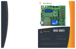
BIG 8051 Manual 1 User Manual Prepared By: BIG 8051 Sajid Amir Josiah Buxton Computer Engineering‘15 Elizabethtown College Computer Engineering ‘15 Elizabethtown College BIG 8051 Manual 2 TABLE OF CONTENTS Page No. 1. General information ……………………………………………………………………………………………….………….………………3 2. Key features…………………………………………………………………………………………………………………….….…………..4 3. Connecting the system to a power source…………………………………………………………………………………………….…..…...5 4. C8051 microcontroller………………………………………………………………………………………………………….……………..6 5. Programming microcontroller……………………………………………………………………………………………….…...…………....7 6. Ethernet module………………………………………………………………………………………………………………….……….…...8 7. Piezo buzzer……………………………………………………………………………………………………….…………………………...9 8. DS 1820 temperature sensor………………………………………………………………………………………………………………….10 9. USB UART module…………………………………………………………………………………………………………………………..11 10. RS-232 modules………………………………………………………………………………………………………………………………12 11. CAN module………………………………………………………………………………………………………………………………….13 12. ZigBee module………………………………………………………………………………………………………………………………..14 13. MMC/SD connector…………………………………………………………………………………………………………………………..15 14. Comparator………………………………………………………………………………………………………………………………........16 15. ADC module………………………………………………………………………………………………………………………………….17 16. DAC module………………………………………………………………………………………………………………………………….18 17. Memory modules……………………………………………………………………………………………………………………………...19 18. LEDs………………………………………………………………………………………………………………………….……………….20 19. Push buttons…………………………………………………………………………………………………………………………………..21 20. I/O ports……………………………………………………………………………………………………………………………………….22 21. 8051 Assembly introduction………………………………………………………………………………………………………………….23 22. Register addressing…………………………………………………………………………………………………………………………...24 23. Instruction set summary………………………………………………………………………………………………………………………25 24. Instruction by opcode ………………………………………………………………………………………………………………………...27 25. Disclaimer……………………………………………………...……………………………………………………………………………..28 BIG 8051 Manual 3 General information The BIG 8051 development system provides a development environment for programming and experimenting with 8051 microcontrollers. Inside the box Development System: BIG8051 CD: Product CD USB Cable 128x64 graphic LCD display 2x16 alphanumeric LCD display Piezo buzzer CAN ZigBee System Specification Power Supply: over AC/DC connector / USB Cable (5V DC) Power Consumption: 50mA (with all modules off) Dimensions: 26.5 x 22 cm Weight: 420g Features Full-featured development system for 8051 Analog to digital conversion of voltage signal CAN communication module Back of BIG8051 development system BIG 8051 Manual 4 Key Features 1. Ethernet module 2. Piezo buzzer 3. Connector for temperature sensor 4. Connector for programmer 21. Jumper used to select push buttons’ logic state 22. Reset button 23. Connector for MMC/SD cards 24. 3.3 V voltage regulator 5. USB UART module (USB power supply connector) 25. Power supply module 6. RS-232B module 26. LEDs 7. Connector for MCU card 27. CAN module 8. RS232B module 28. ZigBee module 9. Comparator 29. Connector for LCD display 10. Jumpers used to select pull-up/pull-down resistors 11. DIP switches used to turn on pull-up/pulldown resistors 12. I/O ports 13. A/D converter inputs 14. D/A converter outputs 15. Memory modules 16. Touch panel controller 17. Connector for GLCD display 18. Connector for touch panel 19. Push buttons 20. Jumper used to shorten protective resistor BIG8051 Board overview[1] BIG 8051 Manual 5 Connecting to power supply To power the development system on, we have to provide power supply voltage over AC/DC connector CN18. Before you turn the system on, it is necessary to place jumper J11 in the EXT position. Next, set the switch marked POWER SUPPLY to the ON position. As soon as the development system now powers on, a green LED labelled POWER will automatically illuminate. Power Supply connector Power supply module connections schematic BIG 8051 Manual 6 C8051F040 microcontroller The BIG8051 system has a 100-pin microcontroller C8051F040 in TQFP package. Today over fifty companies produce variations of the 8051. Several of these companies have over fifty variations of this system. To bring things into context, over 100 million 8051’s are sold each year. Our microcontroller appears to be soldered on the MCU card. Originally, 8051 belongs to the MCS-51 family of microcontrollers. MCS-51 was developed by Intel but other manufacturers are second sources of this family. The MCS-51, now commonly referred to as the 8051 is a Harvard architecture, consisting of physically separate storage and signal pathways for instructions and data. Today, most processors implement such separate signal pathways for performance reasons. The original MCS-51 featured 8-bit ALU, registers, and data busses. The following table shows the features of the MCS-51 and the BIG8051: MCS-51 4K bytes internal ROM 128 bytes internal RAM Four 8-bit I/O ports Two 16-bit timers Serial interface 64K external code memory space 64K external data memory space 210 bit-addressable locations BIG8051 Pipelined instruction architecture executes 70% of instruction set in 1 or 2 system clocks Up to 25 MIPS throughout with 25MHz clock 4352 bytes internal RAM 64kB Flash; in-system programmable 512-byte sectors BOSCH Controller Area Network (CAN 2.0B), hardware SMBus™ (I2C™ Compatible), SPI™, and two UART serial ports available concurrently Internal calibrated programmable oscillator: 3 to 24.5 MHz; etc. The microcontroller can be replaced with another one if desired, but it is important to make sure that they are compatible with the pinouts. “1-wire serial communication enables data to be transferred over one single communication line, while the process itself is under control of the master microcontroller. The advantage of this communication is that only one microcontroller pin is used. All slave devices have unique ID code, which enables the master device to easily identify all devices sharing the same communication bus Microcontroller 8051F040 Pinout [3] BIG 8051 Manual 7 Programming microcontroller The C8051F040 microcontroller must be programmed using a USB DEBUG ADAPTER which is provided with the box. It is always a good practice to make sure that the power is turned on, the USB DEBUG ADAPTER is connected to the development system through the cable as shown(CN23). JTAG programmer USB DEBUG ADAPTER Connecting JTAG Programmer Connector for programmer BIG 8051 Manual 8 Ethernet module The Ethernet module lets us access the LAN network via the connector (RJ45). Using Serial Peripheral Interface, this module can communicate with the microcontroller. Ethernet module Ethernet module connection schematic [4] Connecting Ethernet cable BIG 8051 Manual 9 Piezo Buzzer Piezo buzzers are used for making beeps, tones, and alerts. To use, one pin has to be connected to the ground (in schematic) and the other pin to a square wave out from a timer or microcontroller. For the loudest tones, stay around 4KHz. This buzzer gives the BIG8051 development system the ability to emit audio signals. Best performance for our Piezo buzzer can be achieved with frequencies between 2KHz and 4KHz. To make a connection between the piezo buzzer and the microcontroller, it is necessary to set switch 8 on the DIP switch SW13 to the ON position . The figure currently shows it in off position. Piezo buzzer connected to the microcontroller Piezo buzzer Piezo buzzer and connection schematic [5] BIG 8051 Manual 10 Temperature sensor Our BIG8051 development system comes with a DS1820 temperature sensor that uses 1-wire communication as mentioned earlier. It can be used to measure temperature in the range between –55 degrees Celsius to 125 degree Celsius with an accuracy of +/-0.5 degrees Celsius. The sensor can convert temperature with 9-bit resolution and takes a maximum of 750ms. The communication between this module and the microcontroller is achieved via pin P2.7 as shown in the diagram. To establish a connection between them, it is necessary to set switch 8 on the DIP switch SW15 to the ON position. DS1820 temperature sensor connected. Make sure that the rounded side of the DS1820 matches the half circle on board DS1820 and microcontroller connection schematic [6] Switch 8 on the DIP switch SW15 is set to OFF at the moment. To connect DS1820, set pin P2.7 to ON BIG 8051 Manual 11 USB UART module The USB UART module is used to connect the microcontroller to an external USB device. To establish connection between the microcontroller and the USB UART module, it is important to set switches 1 and 3 (optionally 2 and 4) to the ON position. The BIG8051 can also use this module to power itself. To achieve this, it is necessary to set the switch position of jumper J11 (found on the power module) from EXT to USB. SW13 Connecting USB cable USB UART module USB connector and microcontroller connection schematic [7] BIG 8051 Manual 12 RS-232 modules The RS-232 modules allow the development system to communicate to external devices in compliance with the RS-232 standard. The two RS modules in the BIG8051 can operate separately. To connect, switches 1 and 3 (optionally 2 and 4) on DIP switch SW11 should be set to the ON position. RS-232 module RS-232 module connection schematic [8] BIG 8051 Manual 13 CAN module Controller Area Network (CAN) is a communication standard primarily intended for use in the automotive industry. It is used when microcontrollers and devices need to communicate with each other in applications without a host computer. The modern automobile may have as many as 70 electric control units for various subsystems. Typically the biggest processor is the engine control unit. Others are used for transmission, airbags, ABS, cruise control, electric power steering, audio systems, power windows, doors, mirrors, etc. Some of these form independent subsystems, but communications among others are essential. A subsystem may need to control actuators or receive feedback from sensors. The CAN standard was devised to fill this need. Each CAN node is able to send and receive messages, but not simultaneously. The devices that are usually connected by a CAN network are typically sensors, actuators, and other control devices. The host processor decides what the received messages mean and what messages it wants to transmit. Sensors, actuators and control devices can be connected to the host processor. CAN controller stores the receives serial bits from the bus until an entire message is available, which can then be fetched by the host processer, usually by the CAN controller triggering an interrupt. For sending, the host processor sends the transmit messages to a CAN controller, which transmits the bits serially onto the bus when the bus is free. CAN module connector CAN module To establish connection between this module and the microcontroller, it is necessary to set the switches 1 and 2 on the DIP switch SW12 to the ON position. CAN module and microcontroller connection schematic [9] SW12 BIG 8051 Manual 14 ZigBee module The BIG805 enables you to connect the ZigBee module that is used for wireless communication. The module communicates with the microcontroller with the standard SPI protocols. It is necessary to set switches 1,3 and 5 on the DIP switch SW10, as well as the switches 1,2,3 and 4 on the DIP switch SW15 to the ON position for functionality. At the moment, our boards do not have any RF module attached to it. However, the MRF24J40MA ZigBee module can be connected to the development system. This module can be used as an ideal solution for wireless sensor networks, home automation, building automation, and consumer applications. The features of this particular radio transceiver module are: 2.4 GHz IEEE 8-2.15.4 Transceiver module supports ZigBee™, MiWi™, and MiWi P2P protocols Integrated PCB Antenna with simple four-wire SPI interface to PIC microcontroller Low current consumption BIG 8051 Manual 15 MMC/SD connector The development system is able to read memory cards due to the on-board MMC/SD connector. The module uses microcontroller pins for serial communication. To connect this module, it is necessary to set switches 1,3 and 5 (optionally 2,4, and 6) on the DIP switch SW10, as well as switches 1 and 2 on the DIP switch SW14 to the ON position. BIG 8051 Manual 16 Comparator The BIG8051 can compare voltage levels due to a comparator built into the microcontroller. Voltage signals are supplied via potentiometers P5 and P6. To enable voltage signals, set switches 5 and 6 on DIP switch SW15 to the ON position. BIG 8051 Manual 17 ADC module The ADC module is used to convert an analog voltage level into the appropriate 12-bit digital value. The analog voltage signal is supplied via screw terminals CH0, CH1, CH2, and CH3. The ADC module is built-in into the microcontroller. The voltage supplied from the VREF pin is used as a voltage reference. In order to use this voltage, switch 8 on the DIP SW14 should be set to the ON position. BIG 8051 Manual 18 DAC module . The DAC module attached to the development system can be used to convert 12-bit digital values into appropriate analog voltage values. The output analog voltage signals is delivered via screw terminals DAC0, and DAC1. Like the ADC module, this module also uses the VREF pin on the microcontroller as a voltage reference. To use this voltage, switch 7 on DIP switch SW14 should be set to the ON position. BIG 8051 Manual 19 Memory modules The BIG8051 comes with Flash, RAM and EEPROM memory modules. This allows the microcontroller to expand its memory space. The Flash module lets the microcontroller to use an additional 8Mbit flash memory via SPI. To establish connection between the Flash module and the microcontroller, switches 1, 3, and 5 (optionally 2, 4, and 6) on the DIP switch SW10, as well as switch 7 on the DIP switch SW15 to the ON position. The RAM module enables the microcontroller to use an additional 64Kbit RAM memory via SPI. To enable this connection between the module and the microcontroller, it is necessary to set switches 1,3,5,7 and 8 (optionally 2,4,6) on the DIP switch SW10 to the ON position. EEPROM module enables the microcontroller to use an additional 1Kbit EEPROM memory via I2C serial connection. Set switches 3 and 5 (optionally 4 and 6) on the DIP switch SW12 to the ON position. BIG 8051 Manual 20 LEDs There are a total of 64 LEDs on the development board and can be used to visually indicate the state of each microcontroller I/O pin. When active, an LED indicates that a logic 1 is present on that particular pin. To enable LEDs to illuminate, it is necessary to select the appropriate port using DIP switch SW9. There are 8 available ports labelled PORT0 through PORT7. BIG 8051 Manual 21 Push buttons The provided push buttons on the development board can be used to change the logic state of all the microcontroller input pins. Jumper J10 is used to determine the logic state to be supplied on the appropriate microcontroller pin by pressing a push button. On the lower left side of the push buttons, a RESET button can be found to reset the microcontroller. BIG 8051 Manual 22 Input / Output ports The BIG8051 has 10-pin connectors lined to the microcontroller I/O ports. Due to DIP switches SW1SW8, every connector pin can be connected to one pull-up/pull-down resistor. It depends on the position of jumpers J1-J8 to control this aspect. The pull-up resistor ensures that the signal will be a valid logic level if external devices are connected. A pull up resistor weakly “pulls” the voltage of the wire it is connected to towards its voltage source level when the other components on the line are inactive. A pull-down resistor works the same way but is connected to ground. It holds the logic signal near zero volts when no other device is connected. BIG 8051 Manual 23 8051 Assembly Introduction A computer instruction is made up of an operation code (op-code) followed by either zero, one, or two bytes of operands. address space but are accessed via different addressing modes (direct vs. indirect). The SFR portion can be accessed via direct addressing only. The op-code identifies the type of operation to be performed while the operands identi- There are eight modes of addressing available on the C805. The different addressing fy the source and destination of the data modes determine how the operand byte mentioned earlier to be selected. If the instruction is associated with more than one operand, the format is always: Instruction Destination, Source The direct and indirect addressing modes are used to distinguish between the SFR space and data memory space. The memory map of the C8051 if the lower data RAM area. Addresses 0x00 through 0X1F are banked registers R0-R7. The active bank is controlled via bits in the Program Status Word. From the PSW, we can conclude that the bit addressable memory located from 0x20 through 0x2F which provides 128 bits of bit addressable memory. The upper portion is used general purpose RAM ad can be accessed by any addressing mode (direct or indirect) Special function registers (SFRs) have been added to the C8051 to that of the standard 8051 for enhanced peripherals. Upper data memory and SFR memory share the same BIG 8051 Manual 24 Register Addressing In CPU registers are used to store information temporarily. That information can be in (typically specified in hex format) or by giving its abbreviated name. It is also used for the form of bytes of data to be processed or some address pointing to a data to be SFR accesses. fetched. In 8051 there is only one data type: 8 bits. With an 8 bit data registers, any data more than 8-bit should be divided into 8 bit chunks before being processed. INDIRECT ADDRESSING: The most widely used registers of 8051 are A (accumulator), R0, R1, R2, R3, R4, R5, In the indirect addressing mode, a register is used to hold the effective address of the R6, R7, DPTR (data pointer), PC (program counter). A register is used for all arithme- operand. This register, which holds the address, is called the pointer register and is tic and logic operations. These registers are divided into two groups: said to point to the operand. Only registers R0, R1 and DPTR can be used as pointer registers. DPTR is useful in accessing operands which are in the external memory. General purpose registers Special purpose registers The 8051 microcontroller instructions are divided among five functional groups The register addressing instruction involves information transfer between registers Example: MOV MOV MOV MOV R0, A A,#51H R1,#0FFH R2, #3BH The first instruction above transfers the accumulator content into the R0 register. The register bank (Bank 0,1,2 or 3) must be specified prior to this instruction. # signifies that it is a number and not a byte address ‘H’ symbolizes that it is a hexadecimal number. Similarly if we write a binary number it should end with ‘B’ The ‘0’ in the third instruction in 0FFH symbolizes that the ‘F’ is a hex number and not a letter. This is always necessary if we are writing any hex numbers. It should always start with a 0. All the register should be assumed to be of 1 byte unless otherwise mentioned. Now to transfer contents of R1 to lets say, R6, the following code should do the trick: MOV R6,R1 ; copy contents of R1 to T6 DIRECT ADDRESSING: This mode allows you to specify the operand by giving its actual memory address 1. Arithmetic 2. Logical 3. Data transfer 4. Boolean variable 5. Program branching BIG 8051 Manual 25 Instruction Set Sum- BIG 8051 Manual 26 Instruction Set Summary (cont.) BIG 8051 Manual 27 Instructions by opcode BIG 8051 Manual 28 Writing your first program Download Silicon Laboratories IDE. Follow the link for the download: http://www.silabs.com/Support%20Documents/Software/8BitToolsInstallerweb.exe Download an assembler. Recommended assembler: Keil uVision5 https://www.keil.com/demo/eval/c51.htm After both the installers are downloaded, install the software and run the IDE first Then write your program in assembly language BIG 8051 Manual 29 Writing your first program (cont.) Assembling your code After completing your code, click the assemble button as shown You may be prompted to find an assembler. Browse for the assembler (Keil uVision5) installed earlier. Click rebuild all as shown BIG 8051 Manual 30 Writing your first program (cont.) Connecting the IDE with the development board Before establishing connection between the development board and the IDE, power on the system as instructed earlier. The jumpers J13 and J14 should be in the JTAG position Click options and then select Connection Options from the drop down In the Connection Options dialog box, select the configuration as shown Click connect to establish connection BIG 8051 Manual 31 Downloading and running code on 8051 Click download after connection has been established successfully Then click the GO button as shown Observe results on the board BIG 8051 Manual 32 Disclaimer This manual was prepared strictly for academic use. All the information gathered here have been collected via research and aimed to guide any student to start using the BIG 8051 microcontroller. All the pictures of the development system were taken by Sajid Amir and should not be copied. References: http://www.mikroe.com/downloads/ get/1460/big8051_manual_v100.pdf http://www.silabs.com/Support% 20Documents/ Software/8051_Instruction_Set.pdf http://www.botskool.com/tutorials/ electronics/8051/introduction-8051assembly-language-programming? page=1 http://users.etown.edu/w/wunderjt/ Xilinx%20instructions.pdf http://users.etown.edu/w/wunderjt/ Instructions%20on%2080251% 20Microcontroller%20Board% 20and%20Software%20-% 20SP11WEB2.htm