1
All MikroElektronika´s development systems represent irreplaceable
tools for programming and developing microcontroller-based devices.
Carefully chosen components and the use of machines of the last
generation for mounting and testing thereof are the best guarantee of
high reliability of our devices. Due to simple design, a large number of
add-on modules and ready to use examples, all our users, regardless
of their experience, have the possibility to develop their project in a fast
DQGHI¿FLHQWZD\
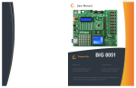
User manual
Development system
BIG8051
™
TO OUR VALUED CUSTOMERS
, ZDQW WR H[SUHVV P\ WKDQNV WR \RX IRU EHLQJ LQWHUHVWHG LQ RXU SURGXFWV DQG IRU KDYLQJ FRQ¿GHQFH LQ
Mikroelektronika.
The primary aim of our company is to design and produce high quality electronic products and to constantly
improve the performance thereof in order to better suit your needs.
Nebojsa Matic
General Manager
The Silicon Laboratories name and logo, the Silicon Laboratories logo, DSPLL®, ISOmodem®, ProSLIC®, SiPHY®, and USBXpress®
are trademarks of Silicon Laboratories Inc. in the U.S.A and other countries.
3
page
BIG8051
TABLE OF CONTENTS
General information .......................................................................................................................... 4
Key features ..................................................................................................................................... 5
1.0. Connecting the development system to a power supply source ................................................ 6
2.0. C8051F040 microcontroller ....................................................................................................... 7
3.0. Programming microcontroller .................................................................................................... 8
4.0. Ethernet module ........................................................................................................................ 9
5.0. Piezo buzzer ............................................................................................................................. 10
6.0. DS1820 temperature sensor .....................................................................................................11
7.0. USB UART module .................................................................................................................... 12
8.0. RS-232 modules ........................................................................................................................ 13
9.0. CAN module .............................................................................................................................. 14
10.0. ZigBee module ........................................................................................................................ 15
11.0. MMC/SD connector ................................................................................................................. 16
12.0. Comparator ............................................................................................................................. 17
13.0. ADC module ............................................................................................................................ 18
14.0. DAC module ............................................................................................................................ 19
15.0. Memory modules ..................................................................................................................... 20
16.0. LEDs ....................................................................................................................................... 22
17.0. Push buttons ........................................................................................................................... 23
18.0. 2x16 LCD display .................................................................................................................... 24
19.0. 128x64 graphic LCD display ................................................................................................... 25
20.0. Touch panel ............................................................................................................................. 26
21.0. I/O ports .................................................................................................................................. 27
MikroElektronika
page
4
BIG8051
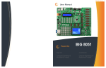
General information
The BIG8051 development system provides a development environment for programming and experimenting with
8051 microcontrollers from Sillicon Labaratories®. Numerous modules, such as 128x64 graphic LCD display, 2x16
alphanumeric LCD display, piezo buzzer, CAN, ZigBee, etc, are provided on the board and allow you to easily simulate
the operation of your target device.
Full-featured development
system for 8051
microcontroller based devices
Analog to digital conversion
of voltage signal
CAN communication module
Access to LAN network
Graphic LCD display with
backlight
3DFNDJHFRQWDLQV
Development system:
CD:
Cables:
Documentation:
BIG8051
product CD with relevant software
USB cable
Manual for BIG8051 and electrical schematic of the
development system
6\VWHPVSHFL¿FDWLRQ
Power supply:
Power consumption:
Dimensions:
Weight:
MikroElektronika
over AC/DC connector (7-23V AC or 9-32V DC)
or a USB cable (5V DC)
50mA when all on-board modules are off
26,5 x 22cm (10,4 x 8,6inch)
~420g (0.92lbs)
5
1
2
3
4
5
6
7
8
9
page
BIG8051
10 11 12
29
28
27
26
25
13
24
23
14
22
21 20
19
18
Key features
1.
2.
3.
4.
5.
6.
7.
8.
9.
10.
11.
12.
13.
Ethernet module
Piezo buzzer
Connector for temperature sensor
Connector for programmer
USB UART module also used as a USB power supply connector
RS-232A module
Connector for MCU card
RS-232B module
Comparator
Jumpers used to select pull-up/pull-down resistors
DIP switches used to turn on pull-up/pull-down resistors
I/O ports
A/D converter inputs
17
16
15
14. D/A converter outputs
15. Memory modules
16. Touch panel controller
17. Connector for GLCD display
18. Connector for touch panel
19. Push buttons
20. Jumper used to shorten protective resistor
21. Jumper used to select push buttons’ logic state
22. Reset button
23. Connector for MMC/SD cards
24. 3.3V voltage regulator
25. Power supply module
26. LEDs
27. CAN module
28. ZigBee module
29. Connector for LCD display
MikroElektronika
page
6
BIG8051
1.0. Connecting the development system to a power supply
In order to enable the development system to be turned on, it is necessary to provide the power supply voltage over an
AC/DC connector CN19, Figure 1-1.
A
B
)LJXUHProviding power supply voltage
Figure 1-2: Power supply module
The power supply voltage provided via the CN19 AC/DC connector may be in a range between 9 and 32V DC or 7 and
23V AC. Before you turn the development system on, it is necessary to place jumper J11 in the EXT position.
When the development system is powered, it is necessary to set switch marked POWER SUPPLY to the ON position. As
soon as the development system is turned on, a green LED marked POWER will automatically illuminate.
)LJXUHPower supply module connection schematic
MikroElektronika
7
page
BIG8051
2.0. C8051F040 microcontroller
The BIG8051 development system comes with a 100-pin microcontroller C8051F040 in TQFP package. The
microcontroller is soldered on the MCU card. It’s key features are as follows:
- Pipelined instruction architecture executes 70% of instruction set in 1 or 2 system clocks;
- Up to 25 MIPS throughput with 25 MHz clock;
- 4352 bytes internal data RAM (4 k + 256);
- 64 kB Flash; in-system programmable in 512-byte sectors;
- Bosch Controller Area Network (CAN 2.0B), hardware SMBus™ (I2C™ Compatible), SPI™, and two UART
serial ports available concurrently;
- Internal calibrated programmable oscillator: 3 to 24.5 MHz; etc.
)LJXUHMicrocontroller C8051F040
)LJXUHMicrocontroller’s pinout
The microcontroller provided on the development system can be easily replaced with another one. When choosing another
microcontroller, it is very important to compare its and C8051F040’s pinouts to make sure that they are compatible. If
you use a microcontroller with different pinout, some on-board modules will probably not work. Anyway, if you decide to
use another microcontroller, it is also necessary to provide an MCU card to solder the new microcontroller on.
MikroElektronika
page
8
BIG8051
3.0. Programming microcontroller
The C8051F040 microcontroller provided on the development system is programmed with a USB DEBUG ADAPTER
that comes with the development system, Figure 3-1.
Before you start programming, it is necessary to turn the
development system on. The external programmer is
connected to the development system via a 2x5 connector
CN23, Figure 3-4. In order to enable the JTAG programmer,
jumpers J13 and J14 should be placed in the JTAG position,
Figure 3-2A. In case the C2 programmer is used, jumpers 13
and J14 should be placed in the C2 position, Figure 3-2B.
A
B
Figure 3-2: Position of jumpers 13 and 14
Figure 3-1: JTAG programmer
A
Figure 3-3: Connector for programmer
MikroElektronika
B
Figure 3-4: Connecting JTAG programmer with the development system
9
page
BIG8051
4.0. Ethernet module
The Ethernet module enables the development system to access the LAN network via the RJ45 connector. The
operation of the Ethernet module is in compliance with the IEEE 802.3 standard. Communication between this module
and the microcontroller is performed via the Serial Peripheral Interface (SPI). In order to enable the Ethernet module
to be connected to the microcontroller, switches 1, 3 and 5 (optionally 2, 4 and 6) on the DIP switch SW10 as well as
switches 5, 6 and 7 on the DIP switch SW13 should be set to the ON position, Figure 4-3.
A
B
Figure 4-2: Connecting ethernet cable
Figure 4-1: Ethernet module
)LJXUHEthernet module connection schematic
MikroElektronika
page
10
BIG8051
5.0. Piezo buzzer
Due to a built-in piezo buzzer, the BIG8051 development system is capable of emitting audio signals. In order to enable
WKHSLH]REX]]HUWRRSHUDWHSURSHUO\LWLVQHFHVVDU\WRJHQHUDWHDYROWDJHVLJQDORIVSHFL¿FIUHTXHQF\5HPHPEHUZKHQ
ZULWLQJWKLVFRGHWKDWWKHSLH]REX]]HU¶VUHVRQDQWIUHTXHQF\LVN+]2WKHUIUHTXHQFLHVLQWKHUDQJHEHWZHHQ+]
DQGN+]FDQDOVREHXVHGEXWWKHEHVWSHUIRUPDQFHLVSURYLGHGZLWKIUHTXHQFLHVUDQJLQJEHWZHHQN+]DQGN+]
To establish connection between the piezo buzzer and the microcontroller, it is necessary to set switch 8 on the DIP
switch SW13 to the ON position.
Figure 5-1: Piezo buzzer
Figure 5-3: Piezo buzzer and microcontroller connection schematic
MikroElektronika
Figure 5-2: Piezo buzzer connected to
the microcontroller pin P2.7
11
page
BIG8051
6.0. DS1820 temperature sensor
1-wire® serial communication enables data to be transferred over one single communication line, while the process
itself is under control of the master microcontroller. The advantage of this communication is that only one microcontroller
pin is used. All slaveGHYLFHVKDYHDXQLTXH,'FRGHZKLFKHQDEOHVWKHmaster device to easily identify all devices
sharing the same communication bus.
DS1820 is a temperature sensor that uses 1-wire communication for its operation. It is used to measure temperature in
a range between -55 and 125°C and provides ±0.5°C accuracy for temperatures in a range between -10 and 85°C. The
power supply voltage of 3V to 5.5V is used for the operation of this sensor. It takes maximum 750ms for the DS1820
to convert temperature with 9-bit resolution. There is a socket for this temperature sensor provided on the BIG8051
development system. Communication between this module and the microcontroller is enabled via the microcontroller
pin P2.7. To establish communication between them, it is also necessary to set switch 8 on the DIP switch SW15 to
the ON position.
NOTE:
Make sure that the
rounded side of the
DS1820 matches halfcircle on the board
Figure 6-1: DS1820
connector (DS1820 is
not connected)
Figure 6-2: Temperature
sensor DS1820 is
connected
Figure 6-3: Switch
8 on the DIP switch
SW15 is in ON
position, DS1820
is connected to the
P2.7 pin
Figure 6-4: DS1820 and microcontroller connection schematic
MikroElektronika
page
12
BIG8051
7.0. USB UART module
The USB UART module is used to connect the microcontroller provided on the development system to external USB
devices. In order to establish connection between the microcontroller and USB UART module, it is necessary to set
switches 1 and 3 (optionally 2 and 4) on the DIP switch SW13 to the ON position. The BIG8051 development system
can also be powered via the USB connector for USB UART module. In this case, it is necessary to switch position of
jumper J11 from EXT to USB.
Figure 7-2: Connecting USB cable
Figure 7-1: USB UART module
Figure 7-3: USB connector and microcontroller connection schematic
MikroElektronika
13
page
BIG8051
8.0. RS-232 modules
The RS-232 modules enable the development system to communicate to external devices whose operation is in
compliance with the RS-232 standard. The BIG8051 development system features two RS-232 modules that operate
independently. To connect the RS-232A module and the microcontroller, switches 1 and 3 (optionally 2 and 4) on the
DIP switch SW11 should be set to the ON position. Similarly, to connect the RS-232B module and the microcontroller,
switches 5 and 7 (optionally 6 and 8) on the DIP switch SW11 should be set to the ON position.
Figure 8-1: RS-232 module
Figure 8-2: RS-232 module connection schematic
MikroElektronika
page
14
BIG8051
9.0. CAN module
CAN (Controller Area Network) is a communication standard primarily intended for use in automotive industry. It enables
the microcontroller to communicate to a device installed in cars without using a host PC. In addition, this communication
is widely used in industrial automation. The BIG8051 development system features CAN module used for communication
with CAN devices. To establish connection between this module and the microcontroller, it is necessary to set switches
1 and 2 on the DIP switch SW12 to the ON position.
Figure 9-1: CAN module
Figure 9-3: CAN module and microcontroller connection schematic
MikroElektronika
Figure 9-2: CAN module connector
15
page
BIG8051
10.0. ZigBee module
The BIG8051 development system enables you to connect the ZigBee module that is used for wireless communication.
Communication between this module and the microcontroller is performed via the Serial Peripheral Interface (SPI). To
enable communication between them, it is necessary to set switches 1, 3 and 5 (optionally 2, 4 and 6) on the DIP switch
SW10, as well as switches 1, 2, 3 and 4 on the DIP switch SW15 to the ON position.
The operation of the ZigBee module is in compliance with the IEEE 802.15.4-2003 standard related to wireless data
transfer on short distances with low-power consumption. The MRF24J40MA ZigBee modul is used on the BIG8051
GHYHORSPHQW V\VWHP 6RPH RI LWV NH\ IHDWXUHV DUH XS WR NESV EDXG UDWH *+] RSHUDWLQJ IUHTXHQF\ aP$
power consumption, up to 400m coverage, etc.
Figure 10-1: MRF24J40MA
ZigBee module
Figure 10-2: Connector for ZigBee
module
Figure 10-3: ZigBee module connection schematic
MikroElektronika
page
16
BIG8051
11.0. MMC/SD connector
The BIG8051 development system is capable of reading memory cards due to the on-board MMC/SD connector. Memory
card communicates with the microcontroller through the microcontroller pins used for serial communication. In order to
establish connection between MMC/SD cards and the microcontroller, it is necessary to set switches 1, 3 and 5 (optionally
2, 4 and 6) on the DIP switch SW10, as well as switches 1 and 2 on the DIP switch SW14 to the ON position.
Figure 11-1: MMC/SD memory card
Figure 11-3: MMC/SD connector and microcontroller connection schematic
MikroElektronika
Figure 11-2: MMC/SD connector
17
page
BIG8051
12.0. Comparator
The BIG8051 development system is capable of comparing voltage levels due to a comparator built into the
microcontroller. Voltage signals are supplied via potentiometers P5 and P6. In order to enable voltage signals, to be
compared, to be supplied to the microcontroller, it is necessary to set switches 5 and 6 on DIP switch SW15 to the ON
position.
Figure 12-1: Comparator
Figure 12-2: Comparator connection schematic
MikroElektronika
page
18
BIG8051
13.0. ADC module
The ADC module is used to convert an analog voltage level into the appropriate 12-bit digital value. The analog voltage
signal is supplied via screw terminals CN15 and CN16. The ADC module is built-in into the microcontroller. The voltage
supplied from the VREF pin is used as a voltage reference. In order to use this voltage, switch 8 on the DIP switch
SW14 should be set to the ON position.
Figure 13-1: ADC module
Figure 13-2: Jumper J9
If the voltage, necessary to perform A/D conversion, is not supplied from an external source, then the 3.3V power
supply voltage is used. In this case, it is necessary to place jumper J9 on the appropriate pins, Figure 13-2.
)LJXUHADC module connection schematic
MikroElektronika
19
page
BIG8051
14.0. DAC module
A DAC module is used to convert 12-bit digital values into appropriate analog voltage values. The analog voltage signal
is delivered via screw terminals CN13 and CN14. The DAC module is built into the microcontroller. The voltage supplied
from the VREF pin on the microcontroller is used as a voltage reference. To enable the use of this voltage, switch 7 on
the DIP switch SW14 should be set to the ON position.
Figure 14-1: DAC module
Figure 14-2: DAC module connector
)LJXUHDAC module connection schematic
MikroElektronika
page
20
BIG8051
15.0. Memory modules
The BIG8051 development system features Flash, RAM and EEPROM memory modules. These modules enable the
microcontroller to expand its memory space.
Figure 15-1: Flash module
Figure 15-2: RAM module
Figure 15-3: EEPROM module
)ODVK PRGXOH HQDEOHV WKH PLFURFRQWUROOHU WR XVH DGGLWLRQDO 0ELW ÀDVK PHPRU\ YLD WKH 6HULDO 3HULSKHUDO ,QWHUIDFH
(SPI). To establish connection between this module and the microcontroller, it is necessary to set switches 1, 3 and 5
(optionally 2, 4 and 6) on the DIP switch SW10, as well as switch 7 on the DIP switch SW15 to the ON position.
)LJXUHFlash module connection schematic
MikroElektronika
RAM module enables the microcontroller to use additional 64Kbit RAM memory via the Serial Peripheral Interface
(SPI). To establish connection between this module and the microcontroller, it is necessary to set switches 1, 3, 5, 7
and 8 (optionally 2, 4 and 6) on the DIP switch SW10 to the ON position.
)LJXUHRAM module connection schematic
EEPROM module enables the microcontroller to use additional 1Kbit EEPROM memory via I2C serial connection. To
establish connection between this module and the microcontroller, it is necessary to set switches 3 and 5 (optionally 4
and 6) on the DIP switch SW12 to the ON position.
)LJXUHEEPROM module connection schematic
MikroElektronika
page
21
BIG8051
page
22
BIG8051
16.0. LEDs
There are 64 LEDs on the BIG8051 development system used to visually indicate the state of each microcontroller
I/O pin. An active LED indicates that a logic one (1) is present on the pin. In order to enable LEDs to illuminate, it is
necessary to select the appropriate port ((PORT0, PORT1, PORT2, PORT3, PORT4, PORT5, PORT6 or PORT7)
using DIP switch SW9.
Notch indicating the
SMD LED cathode
Microcontroller
SMD resistor used to limit
FXUUHQWÀRZWKURXJKDQ/('
Figure 16-1: LEDs
Figure 16-2: LED and port PORT0 connection schematic
MikroElektronika
23
page
BIG8051
17.0. Push buttons
The logic state of all microcontroller input pins may be changed by using push buttons. Jumper J10 is used to determine
the logic state to be supplied on the appropriate microcontroller pin by pressing a push button. The function of the protective resistor is to limit the maximum current, thus preventing the development system and peripheral modules from
being damaged in case a short circuit occurs. If needed, advanced users may shorten this resistor using jumper J12.
Right next to the push buttons, there is a RESET button used to reset the microcontroller.
Figure 17-1: Push buttons
By pressing any push button when jumper J10 is in the VCC position, a logic one (3.3V) will be applied to the appropriate
microcontroller pin, as shown in Figure 17-2.
Figure 17-2: Push buttons and port PORT0 connection schematic
MikroElektronika
page
24
BIG8051
18.0. 2x16 LCD display
The BIG8051 development system features an on-board connector for the alphanumeric 2x16 LCD display. This
connector is linked to the microcontroller via port PORT3. Potentiometer P1 is used to adjust display contrast. The
LCD-BCK switch on the DIP switch SW12 is used to turn the display backlight on/off.
Communication between this LCD and the microcontroller is performed in a 4-bit mode. Alphanumeric digits are displayed in two lines each containing up to 16 characters of 7x5 pixels.
Figure 18-1: Connector for alphanumeric LCD display
)LJXUH2x16 LCD display connection schematic
MikroElektronika
Figure 18-2: Alphanumeric 2x16 LCD display
25
page
BIG8051
19.0. 128x64 graphic LCD display
128x64 graphic LCD (GLCD) is connected to the icrocontroller via PORT2 and PORT4 ports and enables graphic
content to be displayed. It has a screen resolution of 128x64 pixels, which allows diagrams, tables and other graphic
contents to be displayed. Potentiometer P1 is used for the GLCD display contrast adjustment. Switch 8 (GLCD-BCK)
on the DIP switch SW12 is used to turn the display backlight on/off.
)LJXUHGLCD display
)LJXUHGLCD connector
)LJXUH GLCD display connection schematic
MikroElektronika
page
26
BIG8051
20.0. Touch panel
A touch panel is a thin, self-adhesive, transparent, touch-sensitive panel. It is placed over a GLCD display. Its main function
LV WR UHJLVWHU SUHVVXUH DW VRPH VSHFL¿F GLVSOD\ SRLQW DQG WR IRUZDUG LWV FRRUGLQDWHV LQ WKH IRUP RI DQDORJ YROWDJH WR WKH
microcontroller. Switches 3, 4, 5 and 6 on the DIP switch SW14 are used to connect the microcontroller and touch panel.
A
B
C
D
Figure 20-1: Placing touch panel over a GLCD
)LJXUHVKRZVKRZWRSODFHDWRXFKSDQHORYHUD*/&'GLVSOD\0DNHVXUHWKDWWKHÀDWFDEOHLVWRWKHOHIWRIWKH
GLCD, as shown in Figure 20-1D.
Figure 20-2: Touch panel connection schematic
A
C
D
Figure 20-3: Connecting touch panel
)LJXUHVKRZVLQGHWDLOKRZWRFRQQHFWDWRXFKSDQHOWRWKHPLFURFRQWUROOHU%ULQJWKHHQGRIWKHÀDWFDEOHFORVH
WRWKH&1FRQQHFWRU )LJXUH$ 3OXJWKHFDEOHLQWRWKHFRQQHFWRU )LJXUH% DQGSUHVVLWHDVLO\VRDVWRIXOO\¿WWKH
connector (Figure C). Now, a GLCD can be plugged into the appropriate connector (Figure D).
127( LEDs and pull-up/pull-down resistors on ports PORT1 and PORT3 should be off when the touch panel is in use.
MikroElektronika
27
page
BIG8051
21.0. Input/output ports
Along the right side of the development system, there are eight 10-pin connectors linked to the microcontroller I/O ports.
Due to DIP switches SW1-SW8, every connector pin can be connected to one pull-up/pull-down resistor. It depends on
the position of jumpers J1-J8 whether they will be connected to pull-up or pull-down resistor.
)LJXUH J9 in pulldown position
Figure 21-1: I/O ports
)LJXUH J9 in pull-up
position
Figure 21-4: Port PORT7 connection schematic
MikroElektronika
page
28
BIG8051
Pull-up/pull-down resistors enable you to set the logic level on all microcontroller’s input pins when they are in idle state.
This level depends on the position of the pull-up/pull-down jumper. The RP7.0 pin with the relevant DIP switch SW8,
jumper J8 and P7.0 push button with jumper J10 are used here for the purpose of explaining the performance of pull-up/
pull-down resistors. The principle of their operation is the same for all other microcontroller pins.
In order to enable the PORT7 port pins to
be connected to pull-down resistors, it is
necessary to place jumper J8 in the Down
SRVLWLRQ¿UVW7KLVHQDEOHVDQ\3257SRUW
pin to be supplied with a logic zero (0V) in
idle state over jumper J8 and 8x10k resistor
network. To provide the P7.0 pin with this
signal, it is necessary to set switch P7.0 on
the DIP switch SW8 to the ON position.
As a result, every time you press the P7.0
push button, the P7.0 pin will be fed with
a logic one (VCC-3.3 voltage), provided
that jumper J10 is placed in the VCC-3.3
position.
Figure 21-5: Jumper J8 in pull-down and jumper J10 in pull-up position
In order to enable port PORT7 pins to be
connected to pull-up resistors and the port
input pins to be supplied with a logic zero
(0), it is necessary to place jumper J8 in
the Up position and jumper J10 in the GND
position. This enables any port PORT7
input pin, when it is in idle state, to be
driven high (3.3V) over the 10k resistor.
As a result, every time you press the P7.0
push button, the P7.0 pin will be fed with a
logic zero (0V), provided that switch P7.0
on the DIP switch SW8 is set to the ON
position.
)LJXUH Jumper J8 in pull-up and jumper J10 in pull-down position
In case that jumpers J8 and J10 are in the
same positions, pressure on any button will
not cause input pins to change their logic
state.
)LJXUH Jumpers J8 and J10 in the same positions
MikroElektronika
DISCLAIMER
All the products owned by MikroElektronika are protected by copyright law and international copyright treaty.
Therefore, this manual is to be treated as any other copyright material. No part of this manual, including
product and software described herein, may be reproduced, stored in a retrieval system, translated or
transmitted in any form or by any means, without the prior written permission of MikroElektronika. The
PDQXDO3')HGLWLRQFDQEHSULQWHGIRUSULYDWHRUORFDOXVHEXWQRWIRUGLVWULEXWLRQ$Q\PRGL¿FDWLRQRIWKLV
manual is prohibited.
MikroElektronika provides this manual ‘as is’ without warranty of any kind, either expressed or implied,
LQFOXGLQJEXWQRWOLPLWHGWRWKHLPSOLHGZDUUDQWLHVRUFRQGLWLRQVRIPHUFKDQWDELOLW\RU¿WQHVVIRUDSDUWLFXODU
purpose.
MikroElektronika shall assume no responsibility or liability for any errors, omissions and inaccuracies that may
DSSHDULQWKLVPDQXDO,QQRHYHQWVKDOO0LNUR(OHNWURQLNDLWVGLUHFWRUVRI¿FHUVHPSOR\HHVRUGLVWULEXWRUVEH
OLDEOHIRUDQ\LQGLUHFWVSHFL¿FLQFLGHQWDORUFRQVHTXHQWLDOGDPDJHV LQFOXGLQJGDPDJHVIRUORVVRIEXVLQHVV
SUR¿WVDQGEXVLQHVVLQIRUPDWLRQEXVLQHVVLQWHUUXSWLRQRUDQ\RWKHUSHFXQLDU\ORVV DULVLQJRXWRIWKHXVH
of this manual or product, even if MikroElektronika has been advised of the possibility of such damages.
MikroElektronika reserves the right to change information contained in this manual at any time without prior
notice, if necessary.
HIGH RISK ACTIVITIES
The products of MikroElektronika are not fault – tolerant nor designed, manufactured or intended for use or
resale as on – line control equipment in hazardous environments requiring fail – safe performance, such as
LQWKHRSHUDWLRQRIQXFOHDUIDFLOLWLHVDLUFUDIWQDYLJDWLRQRUFRPPXQLFDWLRQV\VWHPVDLUWUDI¿FFRQWUROGLUHFW
life support machines or weapons systems in which the failure of Software could lead directly to death,
SHUVRQDOLQMXU\RUVHYHUHSK\VLFDORUHQYLURQPHQWDOGDPDJH µ+LJK5LVN$FWLYLWLHV¶ 0LNUR(OHNWURQLNDDQGLWV
VXSSOLHUVVSHFL¿FDOO\GLVFODLPDQ\H[SUHVVHGRULPSOLHGZDUUDQW\RI¿WQHVVIRU+LJK5LVN$FWLYLWLHV
TRADEMARKS
The Mikroelektronika name and logo, the Mikroelektronika logo, mikroC, mikroC PRO, mikroBasic, mikro%DVLF352PLNUR3DVFDOPLNUR3DVFDO352$95ÀDVK3,&ÀDVKGV3,&SURJ)-SURJ362&SURJ$95SURJSURJ$50ÀDVK(DV\3,&(DV\3,&%LJ3,&%LJ3,&GV3,&352(DV\%(DV\$50
(DV\$95(DV\$95%LJ$95(DV\GV3,&$(DV\36R&(DV\956WDPS/9)-/9$/90;
3,&0;0XOWL0HGLD%RDUG3,&3/&3,&3/&3,&3/&6PDUW*60*35681,'6DUHWUDGHPDUNV
of Mikroelektronika. All other trademarks mentioned herein are property of their respective companies.
All other product and corporate names appearing in this manual may or may not be registered trademarks
RUFRS\ULJKWVRIWKHLUUHVSHFWLYHFRPSDQLHVDQGDUHRQO\XVHGIRULGHQWL¿FDWLRQRUH[SODQDWLRQDQGWRWKH
RZQHUV¶EHQH¿WZLWKQRLQWHQWWRLQIULQJH
©MikroelektronikaTM$OO5LJKWV5HVHUYHG
,I\RXKDYHDQ\TXHVWLRQVFRPPHQWVRUEXVLQHVVSURSRVDOVGRQRWKHVLWDWHWRFRQWDFWXVDWRI¿FH#PLNURHFRP
If you are experiencing some problems with any of our products or just need additional information, please place your ticket at
www.mikroe.com/en/support
If you want to learn more about our products, please visit our website at www.mikroe.com
Mouser Electronics
Authorized Distributor
Click to View Pricing, Inventory, Delivery & Lifecycle Information:
mikroElektronika:
MIKROE-598