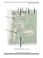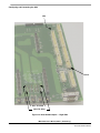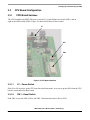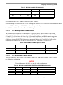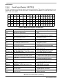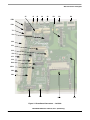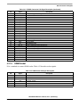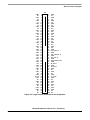
1
i.MX31ADS
Application Development System
User’s Manual
Document Number: MCIMX31ADSRM (UMS-00021)
Rev. 1 (A)
03/2006
Preliminary
How to Reach Us:
Home Page:
www.freescale.com
E-mail:
[email protected]
USA/Europe or Locations Not Listed:
Freescale Semiconductor
Technical Information Center, CH370
1300 N. Alma School Road
Chandler, Arizona 85224
+1-800-521-6274 or +1-480-768-2130
[email protected]
Europe, Middle East, and Africa:
Freescale Halbleiter Deutschland GmbH
Technical Information Center
Schatzbogen 7
81829 Muenchen, Germany
+44 1296 380 456 (English)
+46 8 52200080 (English)
+49 89 92103 559 (German)
+33 1 69 35 48 48 (French)
[email protected]
Japan:
Freescale Semiconductor Japan Ltd.
Headquarters
ARCO Tower 15F
1-8-1, Shimo-Meguro, Meguro-ku,
Tokyo 153-0064, Japan
0120 191014 or +81 3 5437 9125
[email protected]
Asia/Pacific:
Freescale Semiconductor Hong Kong Ltd.
Technical Information Center
2 Dai King Street
Tai Po Industrial Estate
Tai Po, N.T., Hong Kong
+800 2666 8080
[email protected]
Information in this document is provided solely to enable system and software implementers to use
Freescale Semiconductor products. There are no express or implied copyright licenses granted
hereunder to design or fabricate any integrated circuits or integrated circuits based on the information
in this document.
Freescale Semiconductor reserves the right to make changes without further notice to any products
herein. Freescale Semiconductor makes no warranty, representation or guarantee regarding the
suitability of its products for any particular purpose, nor does Freescale Semiconductor assume any
liability arising out of the application or use of any product or circuit, and specifically disclaims any
and all liability, including without limitation consequential or incidental damages. “Typical” parameters
that may be provided in Freescale Semiconductor data sheets and/or specifications can and do vary
in different applications and actual performance may vary over time. All operating parameters,
including “Typicals”, must be validated for each customer application by customer’s technical experts.
Freescale Semiconductor does not convey any license under its patent rights nor the rights of others.
Freescale Semiconductor products are not designed, intended, or authorized for use as components
in systems intended for surgical implant into the body, or other applications intended to support or
sustain life, or for any other application in which the failure of the Freescale Semiconductor product
could create a situation where personal injury or death may occur. Should Buyer purchase or use
Freescale Semiconductor products for any such unintended or unauthorized application, Buyer shall
indemnify and hold Freescale Semiconductor and its officers, employees, subsidiaries, affiliates, and
distributors harmless against all claims, costs, damages, and expenses, and reasonable attorney
fees arising out of, directly or indirectly, any claim of personal injury or death associated with such
unintended or unauthorized use, even if such claim alleges that Freescale Semiconductor was
negligent regarding the design or manufacture of the part.
Freescale™ and the Freescale logo are trademarks of Freescale Semiconductor, Inc. All other
product or service names are the property of their respective owners. ARM is the registered
trademark of ARM Limited. ARM11 is the trademark of ARM Limited.
© Freescale Semiconductor, Inc. 2005, 2006. All rights reserved.
For Literature Requests Only:
Freescale Semiconductor Literature Distribution Center
P.O. Box 5405
Denver, Colorado 80217
1-800-521-6274 or 303-675-2140
Fax: 303-675-2150
[email protected]
Preliminary
Table of Contents
About This Book
Chapter 1 General Information
1.1
1.2
1.3
1.4
Description . . . . . . . . . . . . . . . . . . . . . . . . . . . . . . . . . . . . . . . . . . . . . . . . . . . . . . . . . . . . . . . . 1-1
i.MX31ADS Features . . . . . . . . . . . . . . . . . . . . . . . . . . . . . . . . . . . . . . . . . . . . . . . . . . . . . . . . 1-2
System and User Requirements . . . . . . . . . . . . . . . . . . . . . . . . . . . . . . . . . . . . . . . . . . . . . . . . 1-4
ADS Specifications. . . . . . . . . . . . . . . . . . . . . . . . . . . . . . . . . . . . . . . . . . . . . . . . . . . . . . . . . . 1-4
Chapter 2 Configuring and Connecting the ADS
2.1
Introduction. . . . . . . . . . . . . . . . . . . . . . . . . . . . . . . . . . . . . . . . . . . . . . . . . . . . . . . . . . . . . . . . 2-1
2.2
Base Board Configuration . . . . . . . . . . . . . . . . . . . . . . . . . . . . . . . . . . . . . . . . . . . . . . . . . . . . 2-1
2.2.1
Configuration Switches. . . . . . . . . . . . . . . . . . . . . . . . . . . . . . . . . . . . . . . . . . . . . . . . . . . . 2-1
2.2.1.1
SW1 – UART Enable Switches . . . . . . . . . . . . . . . . . . . . . . . . . . . . . . . . . . . . . . . . . . 2-1
2.2.1.2
SW2 – RS-232 MBaud, Shut Down, WDI, and Buzzer Enable Switches . . . . . . . . . . 2-2
2.2.1.3
SW3 – User Defined Switches . . . . . . . . . . . . . . . . . . . . . . . . . . . . . . . . . . . . . . . . . . . 2-3
2.2.2
Jumper Headers. . . . . . . . . . . . . . . . . . . . . . . . . . . . . . . . . . . . . . . . . . . . . . . . . . . . . . . . . . 2-3
2.3
CPU Board Configuration . . . . . . . . . . . . . . . . . . . . . . . . . . . . . . . . . . . . . . . . . . . . . . . . . . . . 2-7
2.3.1
Switches . . . . . . . . . . . . . . . . . . . . . . . . . . . . . . . . . . . . . . . . . . . . . . . . . . . . . . . . . . . . . . . 2-7
2.3.1.1
S1 – Power Switch . . . . . . . . . . . . . . . . . . . . . . . . . . . . . . . . . . . . . . . . . . . . . . . . . . . . 2-7
2.3.1.2
SW1 – Reset Switch . . . . . . . . . . . . . . . . . . . . . . . . . . . . . . . . . . . . . . . . . . . . . . . . . . . 2-7
2.3.1.3
SW2 – Boot Mode Switches . . . . . . . . . . . . . . . . . . . . . . . . . . . . . . . . . . . . . . . . . . . . . 2-8
2.3.1.4
SW2 – Power-On Reset Switch . . . . . . . . . . . . . . . . . . . . . . . . . . . . . . . . . . . . . . . . . . 2-8
2.3.1.5
SW2 – Reset Out Switch . . . . . . . . . . . . . . . . . . . . . . . . . . . . . . . . . . . . . . . . . . . . . . . 2-8
2.3.1.6
SW2 – Tamper Detect Switch . . . . . . . . . . . . . . . . . . . . . . . . . . . . . . . . . . . . . . . . . . . 2-8
2.3.2
Jumper Headers. . . . . . . . . . . . . . . . . . . . . . . . . . . . . . . . . . . . . . . . . . . . . . . . . . . . . . . . . . 2-8
2.4
Board Configuration . . . . . . . . . . . . . . . . . . . . . . .. . . . . . . . . . . . . . . . . . . . . . . . . . . . . . . . . . 2-11
2.4.1
Switches . . . . . . . . . . . . . . . . . . . . . . . . . . . . . . . . . . . . . . . . . . . . . . . . . . . . . . . . . . . . . . . 2-11
2.4.1.1
S1, S2, S3 – User Defined Push Buttons . . . . . . . . . . . . . . . . . . . . . . . . . . . . . . . . . . . 2-12
2.4.1.2
S4 – USB Function Select, USB Enable, WDI Enable Switches . . . . . . . . . . . . . . . . . 2-12
2.4.1.3
S5 – Backup Source Select Switch . . . . . . . . . . . . . . . . . . . . . . . . . . . . . . . . . . . . . . . . 2-13
2.4.1.4
S6 – USB Buffer Control Switch . . . . . . . . . . . . . . . . . . . . . . . . . . . . . . . . . . . . . . . . . 2-13
2.4.1.5
S7 – Audio Buffer Enable and Direction Select Switch . . . . . . . . . . . . . . . . . . . . . . . . 2-14
2.4.1.6
S8 – CLIA and CLIB Source Select Switch . . . . . . . . . . . . . . . . . . . . . . . . . . . . . . . . . 2-14
2.4.1.7
S9 – MC13783 Power-up Mode Select Switch . . . . . . . . . . . . . . . . . . . . . . . . . . . . . . 2-15
2.4.2
Jumper Headers. . . . . . . . . . . . . . . . . . . . . . . . . . . . . . . . . . . . . . . . . . . . . . . . . . . . . . . . . . 2-15
2.5
ADS Set-up . . . . . . . . . . . . . . . . . . . . . . . . . . . . . . . . . . . . . . . . . . . . . . . . . . . . . . . . . . . . . . . . 2-17
2.5.1
CPU Board Regulator Power Configuration . . . . . . . . . . . . . . . . . . . . . . . . . . . . . . . . . . . 2-17
2.5.2
MC13783 Power Configuration . . . . . . . . . . . . . . . . . . . . . . . . . . . . . . . . . . . . . . . . . . . . . 2-17
2.5.3
Select QVCC and PLL Voltages . . . . . . . . . . . . . . . . . . . . . . . . . . . . . . . . . . . . . . . . . . . . 2-17
i.MX31ADS User’s Manual, REV 1 (Preliminary)
Freescale Semiconductor
i
Table of Contents
2.5.4
2.5.5
2.5.6
2.5.7
2.5.8
2.5.9
2.5.10
2.5.11
2.5.12
2.5.13
Select CPU Clock Source . . . . . . . . . . . . . . . . . . . . . . . . . . . . . . . . . . . . . . . . . . . . . . . . . . 2-18
Set Other CPU Board Jumpers . . . . . . . . . . . . . . . . . . . . . . . . . . . . . . . . . . . . . . . . . . . . . . 2-18
Set CPU Board Switches . . . . . . . . . . . . . . . . . . . . . . . . . . . . . . . . . . . . . . . . . . . . . . . . . . 2-19
Set Base Board Jumpers . . . . . . . . . . . . . . . . . . . . . . . . . . . . . . . . . . . . . . . . . . . . . . . . . . . 2-19
Set Base Board Switches . . . . . . . . . . . . . . . . . . . . . . . . . . . . . . . . . . . . . . . . . . . . . . . . . . 2-19
Connect the CPU Board to the Base Board . . . . . . . . . . . . . . . . . . . . . . . . . . . . . . . . . . . . 2-19
Configure the MC13783 Board . . . . . . . . . . . . . . . . . . . . . . . . . . . . . . . . . . . . . . . . . . . . . 2-20
Connect the MC13783 Board to the Base Board . . . . . . . . . . . . . . . . . . . . . . . . . . . . . . . . 2-21
Connect Power to the CPU Board . . . . . . . . . . . . . . . . . . . . . . . . . . . . . . . . . . . . . . . . . . . 2-21
Turn System Power On . . . . . . . . . . . . . . . . . . . . . . . . . . . . . . . . . . . . . . . . . . . . . . . . . . . 2-21
Chapter 3 ADS Operation
3.1
Functional Block Diagram . . . . . . . . . . . . . . . . . . . . . . . . . . . . . . . . . . . . . . . . . . . . . . . . . . . . 3-1
3.2
ADS Memory Map . . . . . . . . . . . . . . . . . . . . . . . . . . . . . . . . . . . . . . . . . . . . . . . . . . . . . . . . . . 3-2
3.3
Peripheral Bus Control CPLD . . . . . . . . . . . . . . . . . . . . . . . . . . . . . . . . . . . . . . . . . . . . . . . . . 3-3
3.3.1
Features . . . . . . . . . . . . . . . . . . . . . . . . . . . . . . . . . . . . . . . . . . . . . . . . . . . . . . . . . . . . . . . 3-3
3.3.2
CPU Interface . . . . . . . . . . . . . . . . . . . . . . . . . . . . . . . . . . . . . . . . . . . . . . . . . . . . . . . . . . . 3-3
3.3.3
Peripheral Interface . . . . . . . . . . . . . . . . . . . . . . . . . . . . . . . . . . . . . . . . . . . . . . . . . . . . . . 3-4
3.3.3.1
Peripheral Bus Cycles . . . . . . . . . . . . . . . . . . . . . . . . . . . . . . . . . . . . . . . . . . . . . . . . . . 3-4
3.3.3.2
DMA Operation . . . . . . . . . . . . . . . . . . . . . . . . . . . . . . . . . . . . . . . . . . . . . . . . . . . . . . 3-4
3.3.3.3
SC16C652C UART Decode . . . . . . . . . . . . . . . . . . . . . . . . . . . . . . . . . . . . . . . . . . . . . 3-5
3.3.3.4
SCS8900A Ethernet Decode. . . . . . . . . . . . . . . . . . . . . . . . . . . . . . . . . . . . . . . . . . . . . 3-5
3.3.3.5
YMU782B Audio Synthesizer Decode. . . . . . . . . . . . . . . . . . . . . . . . . . . . . . . . . . . . . 3-5
3.3.4
UART Multiplexing . . . . . . . . . . . . . . . . . . . . . . . . . . . . . . . . . . . . . . . . . . . . . . . . . . . . . . 3-5
3.3.5
CPLD Memory Map . . . . . . . . . . . . . . . . . . . . . . . . . . . . . . . . . . . . . . . . . . . . . . . . . . . . . 3-6
3.3.6
Register Descriptions . . . . . . . . . . . . . . . . . . . . . . . . . . . . . . . . . . . . . . . . . . . . . . . . . . . . . 3-6
3.3.6.1
Version Register . . . . . . . . . . . . . . . . . . . . . . . . . . . . . . . . . . . . . . . . . . . . . . . . . . . . . . 3-6
3.3.6.2
Board Status Register 1 (BSTAT1) . . . . . . . . . . . . . . . . . . . . . . . . . . . . . . . . . . . . . . . 3-7
3.3.6.3
Board Status Register 2 (BSTAT2) . . . . . . . . . . . . . . . . . . . . . . . . . . . . . . . . . . . . . . . 3-8
3.3.6.4
Board Control Register 1 (BCTRL1) . . . . . . . . . . . . . . . . . . . . . . . . . . . . . . . . . . . . . . 3-9
3.3.6.5
Board Control Register 2 (BCTRL2) . . . . . . . . . . . . . . . . . . . . . . . . . . . . . . . . . . . . . . 3-10
3.3.6.6
Board Control Register 3 (BCTRL3) . . . . . . . . . . . . . . . . . . . . . . . . . . . . . . . . . . . . . . 3-12
3.3.6.7
Board Control Register 4 (BCTRL4) . . . . . . . . . . . . . . . . . . . . . . . . . . . . . . . . . . . . . . 3-13
3.3.6.8
Interrupt Status/Clear Register (ISCR) . . . . . . . . . . . . . . . . . . . . . . . . . . . . . . . . . . . . . 3-13
3.3.6.9
Interrupt Signal Status Register (ISSR) . . . . . . . . . . . . . . . . . . . . . . . . . . . . . . . . . . . . 3-14
3.3.6.10
Interrupt Mask Register (IMR) . . . . . . . . . . . . . . . . . . . . . . . . . . . . . . . . . . . . . . . . . . . 3-15
3.4
GPIO Interrupt Grouping and Non-registered Interrupts . . . . . . . . . . . . . . . . . . . . . . . . . . . . . 3-15
3.5
On-Board Memory . . . . . . . . . . . . . . . . . . . . . . . . . . . . . . . . . . . . . . . . . . . . . . . . . . . . . . . . . . 3-17
3.6
Using a NAND Flash Card . . . . . . . . . . . . . . . . . . . . . . . . . . . . . . . . . . . . . . . . . . . . . . . . . . . . 3-18
3.7
USB On-The-Go Interface (FS/LS) . . . . . . . . . . . . . . . . . . . . . . . . . . . . . . . . . . . . . . . . . . . . . 3-19
3.8
USB On-The-Go ULPI Interface (HS) . . . . . . . . . . . . . . . . . . . . . . . . . . . . . . . . . . . . . . . . . . . 3-19
3.9
USB HOST ULPI Interface (HS) . . . . . . . . . . . . . . . . . . . . . . . . . . . . . . . . . . . . . . . . . . . . . . . 3-20
3.10 USB HOST Interface (FS/LS) . . . . . . . . . . . . . . . . . . . . . . . . . . . . . . . . . . . . . . . . . . . . . . . . . 3-21
3.11 UART (Internal) and IrDA Interfaces. . . . . . . . . . . . . . . . . . . . . . . . . . . . . . . . . . . . . . . . . . . . 3-21
i.MX31ADS User’s Manual, REV 1 (Preliminary)
ii
Freescale Semiconductor
Table of Contents
3.12
3.13
3.14
3.15
3.16
3.17
3.18
3.19
3.20
3.21
3.22
3.23
3.24
3.25
3.26
3.27
Ethernet Interface . . . . . . . . . . . . . . . . . . . . . . . . . . . . . . . . . . . . . . . . . . . . . . . . . . . . . . . . . . . 3-23
LCD/IPU Interfaces . . . . . . . . . . . . . . . . . . . . . . . . . . . . . . . . . . . . . . . . . . . . . . . . . . . . . . . . . 3-23
Keypad . . . . . . . . . . . . . . . . . . . . . . . . . . . . . . . . . . . . . . . . . . . . . . . . . . . . . . . . . . . . . . . . . . . 3-23
Audio Indicator . . . . . . . . . . . . . . . . . . . . . . . . . . . . . . . . . . . . . . . . . . . . . . . . . . . . . . . . . . . . . 3-24
LED Indicators . . . . . . . . . . . . . . . . . . . . . . . . . . . . . . . . . . . . . . . . . . . . . . . . . . . . . . . . . . . . . 3-24
Sound Synthesizer. . . . . . . . . . . . . . . . . . . . . . . . . . . . . . . . . . . . . . . . . . . . . . . . . . . . . . . . . . . 3-25
Using the TFT LCD Display Panel. . . . . . . . . . . . . . . . . . . . . . . . . . . . . . . . . . . . . . . . . . . . . . 3-25
Using the Keypad . . . . . . . . . . . . . . . . . . . . . . . . . . . . . . . . . . . . . . . . . . . . . . . . . . . . . . . . . . . 3-25
Using the Image Sensor Daughter Card . . . . . . . . . . . . . . . . . . . . . . . . . . . . . . . . . . . . . . . . . . 3-25
Using the TV Encoder . . . . . . . . . . . . . . . . . . . . . . . . . . . . . . . . . . . . . . . . . . . . . . . . . . . . . . . 3-26
Using a Plug in Memory Card . . . . . . . . . . . . . . . . . . . . . . . . . . . . . . . . . . . . . . . . . . . . . . . . . 3-26
Using a PCMCIA Card . . . . . . . . . . . . . . . . . . . . . . . . . . . . . . . . . . . . . . . . . . . . . . . . . . . . . . . 3-26
Using a Mini ATA Hard Drive . . . . . . . . . . . . . . . . . . . . . . . . . . . . . . . . . . . . . . . . . . . . . . . . . 3-27
Using the MC13783 Power Management Board . . . . . . . . . . . . . . . . . . . . . . . . . . . . . . . . . . . 3-27
Using the ETM Connectors . . . . . . . . . . . . . . . . . . . . . . . . . . . . . . . . . . . . . . . . . . . . . . . . . . . 3-27
Using the Samtec Logic Analyzer Connectors . . . . . . . . . . . . . . . . . . . . . . . . . . . . . . . . . . . . . 3-28
Chapter 4 ADS Connectors and Signals
4.1
Introduction. . . . . . . . . . . . . . . . . . . . . . . . . . . . . . . . . . . . . . . . . . . . . . . . . . . . . . . . . . . . . . . . 4-1
4.2
Base Board Connectors. . . . . . . . . . . . . . . . . . . . . . . . . . . . . . . . . . . . . . . . . . . . . . . . . . . . . . . 4-1
4.2.1
Base Board to CPU Board Connectors . . . . . . . . . . . . . . . . . . . . . . . . . . . . . . . . . . . . . . . . 4-5
4.2.2
Base Board to MC13783 Board Connectors . . . . . . . . . . . . . . . . . . . . . . . . . . . . . . . . . . . 4-15
4.2.3
Image Sensor and Extension Connectors . . . . . . . . . . . . . . . . . . . . . . . . . . . . . . . . . . . . . . 4-20
4.2.4
External Keypad Connector . . . . . . . . . . . . . . . . . . . . . . . . . . . . . . . . . . . . . . . . . . . . . . . . 4-26
4.2.5
Display Connectors. . . . . . . . . . . . . . . . . . . . . . . . . . . . . . . . . . . . . . . . . . . . . . . . . . . . . . . 4-28
4.2.5.1
Synchronous LCD Connector . . . . . . . . . . . . . . . . . . . . . . . . . . . . . . . . . . . . . . . . . . . . 4-28
4.2.5.2
Option Connector . . . . . . . . . . . . . . . . . . . . . . . . . . . . . . . . . . . . . . . . . . . . . . . . . . . . . 4-29
4.2.5.3
Parallel LCD Connectors . . . . . . . . . . . . . . . . . . . . . . . . . . . . . . . . . . . . . . . . . . . . . . . 4-30
4.2.5.4
Serial Asynchronous LCD Connector . . . . . . . . . . . . . . . . . . . . . . . . . . . . . . . . . . . . . 4-33
4.2.6
Funlight Connector . . . . . . . . . . . . . . . . . . . . . . . . . . . . . . . . . . . . . . . . . . . . . . . . . . . . . . . 4-34
4.2.7
Audio Connectors . . . . . . . . . . . . . . . . . . . . . . . . . . . . . . . . . . . . . . . . . . . . . . . . . . . . . . . . 4-35
4.2.7.1
Miniature Audio Jacks . . . . . . . . . . . . . . . . . . . . . . . . . . . . . . . . . . . . . . . . . . . . . . . . . 4-35
4.2.7.2
Speaker Terminals . . . . . . . . . . . . . . . . . . . . . . . . . . . . . . . . . . . . . . . . . . . . . . . . . . . . 4-35
4.2.8
Television Encoder Connector . . . . . . . . . . . . . . . . . . . . . . . . . . . . . . . . . . . . . . . . . . . . . . 4-36
4.2.9
ATA Drive Controller Connector . . . . . . . . . . . . . . . . . . . . . . . . . . . . . . . . . . . . . . . . . . . . 4-37
4.2.10
RS-232 Connectors . . . . . . . . . . . . . . . . . . . . . . . . . . . . . . . . . . . . . . . . . . . . . . . . . . . . . . . 4-38
4.2.10.1
DCE Connectors . . . . . . . . . . . . . . . . . . . . . . . . . . . . . . . . . . . . . . . . . . . . . . . . . . . . . . 4-38
4.2.10.2
DTE Connectors . . . . . . . . . . . . . . . . . . . . . . . . . . . . . . . . . . . . . . . . . . . . . . . . . . . . . . 4-40
4.2.11
I2C Connector. . . . . . . . . . . . . . . . . . . . . . . . . . . . . . . . . . . . . . . . . . . . . . . . . . . . . . . . . . . 4-40
4.2.12
CSPI Connector . . . . . . . . . . . . . . . . . . . . . . . . . . . . . . . . . . . . . . . . . . . . . . . . . . . . . . . . . 4-41
4.2.13
Ethernet Connector . . . . . . . . . . . . . . . . . . . . . . . . . . . . . . . . . . . . . . . . . . . . . . . . . . . . . . . 4-42
4.2.14
USB OTG Connectors . . . . . . . . . . . . . . . . . . . . . . . . . . . . . . . . . . . . . . . . . . . . . . . . . . . . 4-42
4.2.15
USB Host Connectors . . . . . . . . . . . . . . . . . . . . . . . . . . . . . . . . . . . . . . . . . . . . . . . . . . . . . 4-43
4.2.16
CE Bus Connector . . . . . . . . . . . . . . . . . . . . . . . . . . . . . . . . . . . . . . . . . . . . . . . . . . . . . . . 4-43
i.MX31ADS User’s Manual, REV 1 (Preliminary)
Freescale Semiconductor
iii
Table of Contents
4.2.17
SD/MMC Connectors . . . . . . . . . . . . . . . . . . . . . . . . . . . . . . . . . . . . . . . . . . . . . . . . . . . . . 4-44
4.2.18
PCMCIA Connector . . . . . . . . . . . . . . . . . . . . . . . . . . . . . . . . . . . . . . . . . . . . . . . . . . . . . . 4-46
4.2.19
SIMM Socket . . . . . . . . . . . . . . . . . . . . . . . . . . . . . . . . . . . . . . . . . . . . . . . . . . . . . . . . . . . 4-47
4.2.20
Baseband Board Connector . . . . . . . . . . . . . . . . . . . . . . . . . . . . . . . . . . . . . . . . . . . . . . . . 4-48
4.2.21
Debugging and Programming Connectors . . . . . . . . . . . . . . . . . . . . . . . . . . . . . . . . . . . . . 4-50
4.2.21.1
Software Analysis Connector . . . . . . . . . . . . . . . . . . . . . . . . . . . . . . . . . . . . . . . . . . . . 4-50
4.2.21.2
Address Connector . . . . . . . . . . . . . . . . . . . . . . . . . . . . . . . . . . . . . . . . . . . . . . . . . . . . 4-50
4.2.21.3
CPLD Programming Connector . . . . . . . . . . . . . . . . . . . . . . . . . . . . . . . . . . . . . . . . . . 4-50
4.2.21.4
One-wire EEPROM Programming . . . . . . . . . . . . . . . . . . . . . . . . . . . . . . . . . . . . . . . . 4-50
4.3
CPU Board Connectors. . . . . . . . . . . . . . . . . . . . . . . . . . . . . . . . . . . . . . . . . . . . . . . . . . . . . . . 4-55
4.3.1
Logic Analyzer Connectors . . . . . . . . . . . . . . . . . . . . . . . . . . . . . . . . . . . . . . . . . . . . . . . . 4-56
4.3.2
ETM Connectors. . . . . . . . . . . . . . . . . . . . . . . . . . . . . . . . . . . . . . . . . . . . . . . . . . . . . . . . . 4-65
4.3.3
RV ICE/JTAG Connector . . . . . . . . . . . . . . . . . . . . . . . . . . . . . . . . . . . . . . . . . . . . . . . . . . 4-69
4.3.4
PC Test Connector . . . . . . . . . . . . . . . . . . . . . . . . . . . . . . . . . . . . . . . . . . . . . . . . . . . . . . . 4-70
4.3.5
In-circuit Serial Programming Connector. . . . . . . . . . . . . . . . . . . . . . . . . . . . . . . . . . . . . . 4-71
4.3.6
NAND Flash Connector . . . . . . . . . . . . . . . . . . . . . . . . . . . . . . . . . . . . . . . . . . . . . . . . . . . 4-71
4.3.7
Memory Stick Connectors . . . . . . . . . . . . . . . . . . . . . . . . . . . . . . . . . . . . . . . . . . . . . . . . . 4-73
4.3.8
Subminiature Clock Connectors . . . . . . . . . . . . . . . . . . . . . . . . . . . . . . . . . . . . . . . . . . . . . 4-73
4.3.9
Power Connector. . . . . . . . . . . . . . . . . . . . . . . . . . . . . . . . . . . . . . . . . . . . . . . . . . . . . . . . . 4-73
4.4 MC13783 Board Connectors . . . . . . . . . . . . . . . . . . . . . . .. . . . . . . . . . . . . . . . . . . . . . . . . . . . 4-74
4.4.1
Power Connectors . . . . . . . . . . . . . . . . . . . . . . . . . . . . . . . . . . . . . . . . . . . . . . . . . . . . . . . . 4-75
4.4.2
Audio Connectors . . . . . . . . . . . . . . . . . . . . . . . . . . . . . . . . . . . . . . . . . . . . . . . . . . . . . . . . 4-75
4.4.2.1
Miniature Audio Jacks . . . . . . . . . . . . . . . . . . . . . . . . . . . . . . . . . . . . . . . . . . . . . . . . . 4-76
4.4.2.2
Audio Terminals . . . . . . . . . . . . . . . . . . . . . . . . . . . . . . . . . . . . . . . . . . . . . . . . . . . . . . 4-76
4.4.3
USB OTG Connector . . . . . . . . . . . . . . . . . . . . . . . . . . . . . . . . . . . . . . . . . . . . . . . . . . . . . 4-77
4.4.4
Touchscreen Connector . . . . . . . . . . . . . . . . . . . . . . . . . . . . . . . . . . . . . . . . . . . . . . . . . . . 4-77
4.4.5
Subminiature Clock Connectors . . . . . . . . . . . . . . . . . . . . . . . . . . . . . . . . . . . . . . . . . . . . . 4-78
i.MX31ADS User’s Manual, REV 1 (Preliminary)
iv
Freescale Semiconductor
List of Figures
Figure 1-1
Figure 2-1
Figure 2-2
Figure 2-3
Figure 2-4
Figure 2-5
Figure 2-6
Figure 2-7
Figure 2-8
Figure 2-9
Figure 3-1
Figure 3-2
Figure 3-3
Figure 3-4
Figure 3-5
Figure 3-6
Figure 3-7
Figure 3-8
Figure 3-9
Figure 3-10
Figure 3-11
Figure 3-12
Figure 3-13
Figure 3-14
Figure 3-15
Figure 3-16
Figure 3-17
Figure 3-18
Figure 3-19
Figure 4-1
Figure 4-2
Figure 4-3
Figure 4-4
Figure 4-5
Figure 4-6
Figure 4-7
Figure 4-8
Figure 4-9
Figure 4-10
Figure 4-11
Figure 4-12
i.MX31ADS Application Development System . . . . . . . . . . . . . . . . . . . . . . . . . . . . . . . 1-1
Base Board Configuration Switches . . . . . . . . . . . . . . . . . . . . . . . . . . . . . . . . . . . . . . . . 2-1
Base Board Jumpers — Left Side . . . . . . . . . . . . . . . . . . . . . . . . . . . . . . . . . . . . . . . . . . 2-5
Base Board Jumpers — Right Side . . . . . . . . . . . . . . . . . . . . . . . . . . . . . . . . . . . . . . . . . 2-6
CPU Board Switches. . . . . . . . . . . . . . . . . . . . . . . . . . . . . . . . . . . . . . . . . . . . . . . . . . . . 2-7
CPU Board Connectors . . . . . . . . . . . . . . . . . . . . . . . . . . . . . . . . . . . . . . . . . . . . . . . . . . 2-11
MC13783 Board Switches . . . . . . . . . . . . .. . . . . . . . . . . . . . . . . . . . . . . . . . . . . . . . . . 2-12
MC13783 Board Jumper Headers. . . . . . . . . . . . . . . . . . . . . . . . . . . . .. . . . . . . . . .. . . . 2-16
Connecting the CPU Board to the Base Board . . . . . . . . . . . . . . . . . . . . . . . . . . . . . . . . 2-20
Connecting the MC13783 Board to the Base Board. . . . . . . . . . . . . . . . . . . . . . . . . . . . 2-21
ADS Functional Block Diagram . . . . . . . . . . . . . . . . . . . . . . . . . . . . . . . . . . . . . . . . . . . 3-1
Version Register . . . . . . . . . . . . . . . . . . . . . . . . . . . . . . . . . . . . . . . . . . . . . . . . . . . . . . . 3-7
Board Status Register 1 (BSTAT1). . . . . . . . . . . . . . . . . . . . . . . . . . . . . . . . . . . . . . . . . 3-7
Board Status Register 2 (BSTAT2). . . . . . . . . . . . . . . . . . . . . . . . . . . . . . . . . . . . . . . . . 3-8
Board Control Register 1 (BCTRL1) . . . . . . . . . . . . . . . . . . . . . . . . . . . . . . . . . . . . . . . 3-9
Board Control Register 2 (BCTRL2) . . . . . . . . . . . . . . . . . . . . . . . . . . . . . . . . . . . . . . . 3-10
Board Control Register 3 (BCTRL3) . . . . . . . . . . . . . . . . . . . . . . . . . . . . . . . . . . . . . . . 3-12
Board Control Register 4 (BCTRL4) . . . . . . . . . . . . . . . . . . . . . . . . . . . . . . . . . . . . . . . 3-13
Interrupt Status/Clear Register (ISCR) . . . . . . . . . . . . . . . . . . . . . . . . . . . . . . . . . . . . . . 3-14
Interrupt Signal Current State Status Register (ISCSSR) . . . . . . . . . . . . . . . . . . . . . . . . 3-14
Interrupt Mask Register (IMR) . . . . . . . . . . . . . . . . . . . . . . . . . . . . . . . . . . . . . . . . . . . . 3-15
Burst Flash and PSRAM Interface . . . . . . . . . . . . . . . . . . . . . . . . . . . . . . . . . . . . . . . . . 3-17
DDR SDRAM Interface . . . . . . . . . . . . . . . . . . . . . . . . . . . . . . . . . . . . . . . . . . . . . . . . . 3-18
USB OTG (FS/LS) Interface. . . . . . . . . . . . . . . . . . . . . . . . . . . . . . . . . . . . . . . . . . . . . . 3-19
USB OTG HS ULPI Interface. . . . . . . . . . . . . . . . . . . . . . . . . . . . . . . . . . . . . . . . . . . . . 3-20
USB HS HOST ULPI Interface . . . . . . . . . . . . . . . . . . . . . . . . . . . . . . . . . . . . . . . . . . . 3-20
USB FS/LS HOST Interface . . . . . . . . . . . . . . . . . . . . . . . . . . . . . . . . . . . . . . . . . . . . . . 3-21
UARTs and IrDA Interface . . . . . . . . . . . . . . . . . . . . . . . . . . . . . . . . . . . . . . . . . . . . . . 3-22
Ethernet Interface . . . . . . . . . . . . . . . . . . . . . . . . . . . . . . . . . . . . . . . . . . . . . . . . . . . . . . 3-23
Base Board Connectors — Left Side . . . . . . . . . . . . . . . . . . . . . . . . . . . . . . . . . . . . . . . 4-3
Base Board Connectors — Right Side . . . . . . . . . . . . . . . . . . . . . . . . . . . . . . . . . . . . . . 4-4
Base Board to CPU Board Connectors P1 and P2 Pin Assignment . . . . . . . . . . . . . . . . 4-6
Base Board to MC13783 Board Connectors P5 and P6 Pin Assignment . . . . . . . . . . . . 4-16
Image Sensor and Extension Connector Pin Numbering . . . . . . . . . . . . . . . . . . . . . . . . 4-21
External Keypad Connector P5 Pin Assignment. . . . . . . . . . . . . . . . . . . . . . . . . . . . . . . 4-26
Synchronous LCD Connector J12 Pin Assignment . . . . . . . . . . . . . . . . . . . . . . . . . . . . 4-28
Option Connector J11 Pin Assignment . . . . . . . . . . . . . . . . . . . . . . . . . . . . . . . . . . . . . . 4-29
Parallel LCD Connector I J9 Pin Assignment. . . . . . . . . . . . . . . . . . . . . . . . . . . . . . . . . 4-30
Parallel LCD Connector II J8 Pin Assignment . . . . . . . . . . . . . . . . . . . . . . . . . . . . . . . . 4-32
Serial Asynchronous LCD Connector J6 Pin Assignment . . . . . . . . . . . . . . . . . . . . . . . 4-33
Funlight Connector J20 Pin Assignment. . . . . . . . . . . . . . . . . . . . . . . . . . . . . . . . . . . . . 4-34
i.MX31ADS User’s Manual, REV 1 (Preliminary)
Freescale Semiconductor
v
List of Figures
Figure 4-13
Figure 4-14
Figure 4-15
Figure 4-16
Figure 4-17
Figure 4-18
Figure 4-19
Figure 4-20
Figure 4-21
Figure 4-22
Figure 4-23
Figure 4-24
Figure 4-25
Figure 4-26
Figure 4-27
Figure 4-28
Figure 4-29
Figure 4-30
Figure 4-31
Figure 4-32
Figure 4-33
Figure 4-34
Figure 4-35
Figure 4-36
Figure 4-37
Figure 4-38
Figure 4-39
Figure 4-40
Figure 4-41
Figure 4-42
Figure 4-43
Audio Jack Diagram . . . . . . . . . . . . . . . . . . . . . . . . . . . . . . . . . . . . . . . . . . . . . . . . . . . . 4-35
TV Encoder Connector P13 Pin Assignment . . . . . . . . . . . . . . . . . . . . . . . . . . . . . . . . . 4-36
ATA Connector J3 Pin Assignment . . . . . . . . . . . . . . . . . . . . . . . . . . . . . . . . . . . . . . . . 4-37
RS-232 DCE Connectors P7A and P7B Pin Assignment . . . . . . . . . . . . . . . . . . . . . . . 4-39
RS-232 DCE Connector J7 Pin Assignment . . . . . . . . . . . . . . . . . . . . . . . . . . . . . . . . . . 4-39
RS-232 DTE Connectors P11A and P11B Pin Assignment . . . . . . . . . . . . . . . . . . . . . . 4-40
CSPI Connector J15 Pin Assignment . . . . . . . . . . . . . . . . . . . . . . . . . . . . . . . . . . . . . . . 4-41
Ethernet Connector T1 Pin Numbers . . . . . . . . . . . . . . . . . . . . . . . . . . . . . . . . . . . . . . . 4-42
USB OTG Connectors J1 and J2 Pin Assignment . . . . . . . . . . . . . . . . . . . . . . . . . . . . . 4-42
USB Host Connectors J4 and J5 Pin Assignment . . . . . . . . . . . . . . . . . . . . . . . . . . . . . . 4-43
CE Bus Connector J19 Pin Assignment . . . . . . . . . . . . . . . . . . . . . . . . . . . . . . . . . . . . . 4-43
SD/MMC Connector Pin Assignments . . . . . . . . . . . . . . . . . . . . . . . . . . . . . . . . . . . . . 4-44
Baseband Board Connector J24 Pin Assignment . . . . . . . . . . . . . . . . . . . . . . . . . . . . . . 4-48
Software Analysis Connector P9 Pin Assignment . . . . . . . . . . . . . . . . . . . . . . . . . . . . . 4-51
Address Connector P10 Pin Assignment . . . . . . . . . . . . . . . . . . . . . . . . . . . . . . . . . . . . 4-52
CPLD Programming Connector J14 Pin Assignment . . . . . . . . . . . . . . . . . . . . . . . . . . . 4-54
CPU Board Connectors . . . . . . . . . . . . . . . . . . . . . . . . . . . . . . . . . . . . . . . . . . . . . . . . . . 4-56
Logic Analyzer Connector P2 Pin Assignment. . . . . . . . . . . . . . . . . . . . . . . . . . . . . . . . 4-57
Logic Analyzer Connector P3 Pin Assignment. . . . . . . . . . . . . . . . . . . . . . . . . . . . . . . . 4-59
Logic Analyzer Connector P5 Pin Assignment. . . . . . . . . . . . . . . . . . . . . . . . . . . . . . . . 4-61
Logic Analyzer Connector P6 Pin Assignment. . . . . . . . . . . . . . . . . . . . . . . . . . . . . . . . 4-63
Primary ETM Connector P4 Pin Assignment . . . . . . . . . . . . . . . . . . . . . . . . . . . . . . . . . 4-65
Alternate ETM Connector P1 Pin Assignment . . . . . . . . . . . . . . . . . . . . . . . . . . . . . . . . 4-67
RV ICE/JTAG Connector J8 Pin Assignment . . . . . . . . . . . . . . . . . . . . . . . . . . . . . . . . 4-69
PC Test Connector J4 Pin Assignment . . . . . . . . . . . . . . . . . . . . . . . . . . . . . . . . . . . . . . 4-70
ISP Connector J7 Pin Assignment . . . . . . . . . . . . . . . . . . . . . . . . . . . . . . . . . . . . . . . . . 4-71
NAND Flash Connector J9 Pin Assignment . . . . . . . . . . . . . . . . . . . . . . . . . . . . . . . . . 4-71
MC13783 Board Connectors . . . . . . . . . . . . . . . . . . . .. . . . . . . . . . . . . . . .. . . . . . . . . . 4-75
Audio Jack Diagram . . . . . . . . . . . . . . . . . . . . . . . . . . . . . . . . . . . . . . . . . . . . . . . . . . . . 4-76
USB OTG Connector CN3 Pin Assignment . . . . . . . . . . . . . . . . . . . . . . . . . . . . . . . . . . 4-77
Touchscreen Connector CN8 Pin Assignment . . . . . . . . . . . . . . . . . . . . . . . . . . . . . . . . 4-77
i.MX31ADS User’s Manual, REV 1 (Preliminary)
vi
Freescale Semiconductor
List of Tables
Table 1-1
Table 2-1
Table 2-2
Table 2-3
Table 2-4
Table 2-5
Table 2-6
Table 2-7
Table 2-8
Table 2-9
Table 2-10
Table 2-11
Table 2-12
Table 2-13
Table 3-1
Table 3-2
Table 3-3
Table 3-4
Table 3-5
Table 3-6
Table 3-7
Table 3-8
Table 3-9
Table 3-10
Table 3-11
Table 3-12
Table 3-13
Table 3-14
Table 3-15
Table 3-16
Table 3-17
Table 4-1
Table 4-2
Table 4-3
Table 4-4
Table 4-5
Table 4-6
Table 4-7
Table 4-8
Table 4-9
Table 4-10
Specifications . . . . . . . . . . . . . . . . . . . . . . . . . . . . . . . . . . . . . . . . . . . . . . . . . . . . . . . . 1-4
Base Board SW1 Switch function. . . . . . . . . . . . . . . . . . . . . . . . . . . . . . . . . . . . . . . . . .2- 2
Base Board SW2 Switch Function . . . . . . . . . . . . . . . . . . . . . . . . . . . . . . . . . . . . . . . . .2- 2
SW3 Switch Settings. . . . . . . . . . . . . . . . . . . . . . . . . . . . . . . . . . . . . . . . . . . . . . . . . . . .2- 3
Base Board Jumper Headers . . . . . . . . . . . . . . . . . . . . . . . . . . . . . . . . . . . . . . . . . . . . . .2- 3
Boot Mode Switch Settings. . . . . . . . . . . . . . . . . . . . . . . . . . . . . . . . . . . . . . . . . . . . . . .2- 8
CPU Board Jumper Headers . . . . . . . . . . . . . . . . . . . . . . . . . . . . . . . . . . . . . . . . . . . . . .2- 9
MC13783 Board S4 USB Mode Select. . . . . . . . . . . . . . . . .. . .. . . . . . . . . . . . . . . . . . .2- 13
MC13783 Board S5 Backup Source Select . . . . . . . . . . . . . . . . . . . . . . . . . .. . . . . . . 2-13
MC13783 Board SW6 USB UDATVP and USBOVM Direction Select. . . . . . . . . . . .2- 13
MC13783 Board SW7 Buffer Enable and Direction Select . . . . . . . . . . . . . . . . . . . . . . 2-14
MC13783 Board SW8 CLIA and CLIB Source Select. . . . . . . . . . . . . . . . . . . . . . . . . . 2-14
MC13783 Board SW9 MC13783 Power-up Mode Select . . . . . . . . . . . . . . . . . . . . . . .2- 15
MC13783 Board Jumper Headers. . . . . . . . . . . . . . . . . . . . . . . . . . . . . . . . . . . . . . . . . . 2-15
ADS Memory Map . . . . . . . . . . . . . . . . . . . . . . . . . . . . . . . . . . . . . . . . . . . . . . . . . . . . . 3 - 2
CPU Signal Interface. . . . . . . . . . . . . . . . . . . . . . . . . . . . . . . . . . . . . . . . . . . . . . . . . . . .3- 3
Peripheral Interface Signals . . . . . . . . . . . . . . . . . . . . . . . . . . . . . . . . . . . . . . . . . . . . . . 3 - 4
Bus Cycles. . . . . . . . . . . . . . . . . . . . . . . . . . . . . . . . . . . . . . . . . . . . . . . . . . . . . . . . . . . .3- 4
CPLD Memory Map . . . . . . . . . . . . . . . . . . . . . . . . . . . . . . . . . . . . . . . . . . . . . . . . . . . . 3 - 6
Board Status Register 1 Bit Definitions . . . . . . . . . . . . . . . . . . . . . . . . . . . . . . . . . . . . .3- 8
Board Status Register 1 Bit Definitions . . . . . . . . . . . . . . . . . . . . . . . . . . . . . . . . . . . . .3- 8
Board Control Register 1 Bit Definitions . . . . . . . . . . . . . . . . . . . . . . . . . . . . . . . . . . . . 3-10
Board Control Register 2 Bit Definitions . . . . . . . . . . . . . . . . . . . . . . . . . . . . . . . . . . . .3- 11
Board Control Register 3 Bit Definitions . . . . . . . . . . . . . . . . . . . . . . . . . . . . . . . . . . . . 3-12
Board Control Register 4 Bit Definitions . . . . . . . . . . . . . . . . . . . . . . . . . . . . . . . . . . . .3- 13
Interrupt Status/Clear Register Bit Definitions . . . . . . . . . . . . . . . . . . . . . . . . . . . . . . . . 3-14
Interrupt Signal Status Register Bit Definitions . . . . . . . . . . . . . . . . . . . . . . . . . . . . . . .3- 15
GPIO Interrupt Grouping . . . . . . . . . . . . . . . . . . . . . . . . . . . . . . . . . . . . . . . . . . . . . . . . 3 - 15
GPIO Interrupt Bit Descriptions . . . . . . . . . . . . . . . . . . . . . . . . . . . . . . . . . . . . . . . . . . .3- 16
Keypad Layout and Connections . . . . . . . . . . . . . . . . . . . . . . . . . . . . . . . . . . . . . . . . . . 3-24
Function of LED Indicators . . . . . . . . . . . . . . . . . . . . . . . . . . . . . . . . . . . . . . . . . . . . . . 3 - 24
Base Board Connectors . . . . . . . . . . . . . . . . . . . . . . . . . . . . . . . . . . . . . . . . . . . . . . . . . . 4 - 1
Base Board to CPU Board Connector P1 Signal Description. . . . . . . . . . . . . . . . . . . . .4- 7
Base Board to CPU Board Connector P2 Signal Description. . . . . . . . . . . . . . . . . . . . . 4-11
Base Board to MC13783 Board Connector P5 Signal Description . . . . . . . . . . . . . . . .4- 17
Base Board to MC13783 Board Connector P6 Signal Description . . . . . . . . . . . . . . . . 4-17
Image Sensor Connectors J10 and J13 Signal Description . . . . . . . . . . . . . . . . . . . . . . .4- 21
Extension Connector J17 Signal Description . . . . . . . . . . . . . . . . . . . . . . . . . . . . . . . . . 4-22
Extension Connector J22 Signal Description . . . . . . . . . . . . . . . . . . . . . . . . . . . . . . . . .4- 24
Extension Connector J23 Signal Description . . . . . . . . . . . . . . . . . . . . . . . . . . . . . . . . . 4-25
External Keypad Connector P5 Signal Description . . . . . . . . . . . . . . . . . . . . . . . . . . . .4- 27
i.MX31ADS User’s Manual, REV 1 (Preliminary)
Freescale Semiconductor
vii
List of Tables
Table 4-11 Synchronous LCD Connector J12 Signal Description . . . . . . . . . . . . . . . . . . . . . . . . . . 4-28
Table 4-12 Option Connector J11 Signal Description. . . . . . . . . . . . . . . . . . . . . . . . . . . . . . . . . . . .4- 30
Table 4-13 Parallel LCD Connector I J9 Signal Description . . . . . . . . . . . . . . . . . . . . . . . . . . . . . . 4-31
Table 4-14 Parallel LCD Connector II J8 Signal Description. . . . . . . . . . . . . . . . . . . . . . . . . . . . . .4- 32
Table 4-15 Serial Asynchronous LCD Connector J6 Signal Description . . . . . . . . . . . . . . . . . . . . . 4-34
Table 4-16 Funlight Connector J20 Signal Description . . . . . . . . . . . . . . . . . . . . . . . . . . . . . . . . . .4- 35
Table 4-17 Audio Jack Signal Description . . . . . . . . . . . . . . . . . . . . . . . . . . . . . . . . . . . . . . . . . . . . 4-36
Table 4-18 TV Encoder Connector P13 Signal Description . . . . . . . . . . . . . . . . . . . . . . . . . . . . . . .4- 36
Table 4-19 ATA Connector J3 Signal Description . . . . . . . . . . . . . . . . . . . . . . . . . . . . . . . . . . . . . . 4-37
Table 4-20 RS-232 DCE Connectors P7A and P7B Signal Description . . . . . . . . . . . . . . . . . . . . .4- 39
Table 4-21 RS-232 DCE Connector J7 Pin Signal Description . . . . . . . . . . . . . . . . . . . . . . . . . . . .4-39
Table 4-22 RS-232 DTE Connectors P11A and P11B Signal Description . . . . . . . . . . . . . . . . . . . . 4-40
Table 4-23 I2C Connector JP13 Signal Description . . . . . . . . . . . . . . . . . . . . . . . . . . . . . . . . . . . . .4- 40
Table 4-24 CSPI Connector J15 Signal Description . . . . . . . . . . . . . . . . . . . . . . . . . . . . . . . . . . . . . 4-41
Table 4-25 Ethernet Connector T1 Signal Description . . . . . . . . . . . . . . . . . . . . . . . . . . . . . . . . . .4- 42
Table 4-26 USB OTG Connectors J1 andJ2 Signal Description. . . . . . . . . . . . . . . . . . . . . . . . . . . . 4-42
Table 4-27 USB Host Connectors J4 and J5 Signal Description. . . . . . . . . . . . . . . . . . . . . . . . . . . .4- 43
Table 4-28 CE Bus Connector J19 Signal Description . . . . . . . . . . . . . . . . . . . . . . . . . . . . . . . . . . . 4-44
Table 4-29 SD/MMC Connector P3 Signal Description . . . . . . . . . . . . . . . . . . . . . . . . . . . . . . . . .4- 45
Table 4-30 SD/MMC Connector P4 Signal Description . . . . . . . . . . . . . . . . . . . . . . . . . . . . . . . . . . 4-45
Table 4-31 PCMCIA Connector U30 Signal Description . . . . . . . . . . . . . . . . . . . . . . . . . . . . . . . . .4- 46
Table 4-32 SIMM Socket P8 Signal Description . . . . . . . . . . . . . . . . . . . . . . . . . . . . . . . . . . . . . . . 4-47
Table 4-33 Baseband Board Connector J24 Signal Description . . . . . . . . . . . . . . . . . . . . . . . . . . . .4- 49
Table 4-34 Software Analysis Connector P9 Signal Description . . . . . . . . . . . . . . . . . . . . . . . . . . . 4-51
Table 4-35 Address Connector P10 Signal Description . . . . . . . . . . . . . . . . . . . . . . . . . . . . . . . . . .4- 53
Table 4-36 CPLD Programming Connector J14 Signal Description. . . . . . . . . . . . . . . . . . . . . . . . . 4-54
Table 4-37 CPU Board Connectors . . . . . . . . . . . . . . . . . . . . . . . . . . . . . . . . . . . . . . . . . . . . . . . . . . 4 - 55
Table 4-38 Logic Analyzer Connector P2 Signal Description . . . . . . . . . . . . . . . . . . . . . . . . . . . . .4- 58
Table 4-39 Logic Analyzer Connector P3 Signal Description . . . . . . . . . . . . . . . . . . . . . . . . . . . . . 4-60
Table 4-40 Logic Analyzer Connector P5 Signal Description . . . . . . . . . . . . . . . . . . . . . . . . . . . . .4- 62
Table 4-41 Logic Analyzer Connector P6 Signal Description . . . . . . . . . . . . . . . . . . . . . . . . . . . . . 4-64
Table 4-42 Primary ETM Connector P4 Signal Description. . . . . . . . . . . . . . . . . . . . . . . . . . . . . . .4- 66
Table 4-43 Alternate ETM Connector P1 Signal Description. . . . . . . . . . . . . . . . . . . . . . . . . . . . . . 4-68
Table 4-44 RV ICE/JTAG Connector J8 Signal Description . . . . . . . . . . . . . . . . . . . . . . . . . . . . . .4- 69
Table 4-45 PC Test Connector J4 Signal Description . . . . . . . . . . . . . . . . . . . . . . . . . . . . . . . . . . . . 4-70
Table 4-46 ISP Connector J7 Signal Description . . . . . . . . . . . . . . . . . . . . . . . . . . . . . . . . . . . . . . .4- 71
Table 4-47 NAND Flash Connector J9 Signal Description . . . . . . . . . . . . . . . . . . . . . . . . . . . . . . . 4-72
Table 4-48 Memory Stick Connector J5 Signal Description. . . . . . . . . . . . . . . . . . . . . . . . . . . . . . .4- 73
Table 4-49 Memory Stick Connector J6 Signal Description. . . . . . . . . . . . . . . . . . . . . . . . . . . . . . . 4-73
Table 4-50 MC13783 Board Connectors . . . . . . . . . . . . . . . . . . . . . . . . . . . . . . . . . . . . . . . . . . . . . 4-74
Table 4-51 Audio Jack Signal Descriptions . . . . . . . . . . . . . . . . . . . . . . . . . . . . . . . . . . . . . . . . . . .4- 76
Table 4-52 USB Connector CN3 Signal Description . . . . . . . . . . . . . . . . . . . . . . . . . . . . . . . . . . . . 4-77
Table 4-53 Touchscreen Connector CN8 Signal Description . . . . . . . . . . . . . . . . . . . . . . . . . . . . . .4- 77
i.MX31ADS User’s Manual, REV 1 (Preliminary)
viii
Freescale Semiconductor
About This Book
This manual explains how to connect and operate the i.MX31ADS Application Development System.
Audience
The audience for this manual is handheld communication device designers. It is assumed that users are
engineers or technicians with experience using development systems.
Organization
The manual consists of three chapters.
• Chapter 1 introduces the user to the features and capabilities of the ADS.
• Chapter 2 provides configuration and set-up information.
• Chapter 3 provide operational information.
• Chapter 4 provides connector locations, functions, pin assignments, and signal descriptions.
Revision History
This is a new document.
Conventions
Units and measures in this manual conform to the International System of Units (SI) as defined by
United States National Institute of Standards and Technology Special Publication 811.
Ranges of bits and signals are shown in square brackets: A[15:0].
Individual signals and bits within a range are shown with a numeric designator only: A7.
Logic level 0 is the voltage that corresponds to Boolean 0; logic level 1 is the voltage that corresponds to
Boolean 1.
When a signal is asserted, it goes to the active logic state. Active-high signals go to logic level 1;
active-low signals go to logic level 0.
When a signal is negated, it goes to the inactive logic state. Active-high signals go to logic level 0;
active-low signals go to logic level 1.
Setting a bit refers specifically to establishing logic level 1 on the bit; clearing a bit refers specifically to
establishing logic level 0 on the bit. Ranges of bits may be set or cleared by a single operation.
Overbars are used to show active-low or complemented signals and bits in text: SIGNAL, BIT.
Active-low signal names are designated by the suffix “_b”: signal_name_b.
i.MX31ADS User’s Manual, REV 1 (Preliminary)
Freescale Semiconductor
ix
Acronyms and Abbreviations
The following acronyms and abbreviations are used in this manual. This list does not include signal,
register, and software mnemonics.
ADS
Application Development System
APMSMC13783 Power Management System
ATA
Hard drive interface spec
CD
Compact Disk
CMOS
Complementary Metal Oxide Semiconductor
CPLD
Custom Programmed Logic Devices
CPU
Central Processing Unit
CSI
Camera Sensor Imaging
CSPI
Serial Peripheral Interface
DCE
DDR
DIN
DIP
DMA
DTE
DUART
EEPROM
EPROM
FIR
GPIO
I2C
ICE
I/O
IrDA
ISA
JTAG
LAN
LCD
LED
MB
MCU
MMC
Data Communications Equipment
Double Data Rate
Deutsches Institut für Normung
Dual In-line Package
Direct Memory Access
Data Terminal Equipment
Dual Universal Asynchronous Receiver/Transmitter
Electrically Eraseable Programmable Read Only Memory
Eraseable Programmable Read Only Memory
Infra Red
General Purpose Input/Output
Inter-Integrated Circuit
In-Circuit Emulator
Input/Output
Infrared Data Association
Instrumentation, System, and Automation Society
Joint Test Access Group
Local Area Network
Liquid Crystal Display
Light Emitting Diode
Megabyte
Microcontroller Unit
Multi-media Card
i.MX31ADS User’s Manual, REV 1 (Preliminary)
x
Freescale Semiconductor
MCP
MS
NVRAM
OTG
PC
PCMCIA
PCB
PCMCIA
PHY
POR
PSRAM
PWM
QVGA
RAM
SD
SDRAM
SI
SIMM
SPST
SSI
TFT
UART
USB
Multi-chip product
Memory Stick
Non-volatile Random Access Memory
On the Go
Personal Computer
Personal Computer Memory Card International Association
Printed Circuit Board
Personal Computer Memory Card International Association
Physical interface
Power On Reset
Pseudo Random Access Memory
Pulse Width Modulation
Graphics Adapter
Random Access Memory
Smart Digital
Synchronous Dynamic Random Access Memory
Systeme International (international system of units and measures)
Single In-Line Memory Module
Single Pole Single Throw
Synchronous Serial Interface
Thin Film Transistor
Universal Asynchronous Receiver/Transmitter
Universal Serial Bus
i.MX31ADS User’s Manual, REV 1 (Preliminary)
Freescale Semiconductor
xi
i.MX31ADS User’s Manual, REV 1 (Preliminary)
xii
Freescale Semiconductor
Chapter 1 General Information
1.1
Description
The i.MX31ADS helps you develop multimedia communication applications using the i.MX31's ARM11
MCU and the MC13783 audio and power management chip.
The ADS consists of a Base board, a CPU board, and an MC13783 board. The system supports application
software development, target board debugging, and optional circuit cards. The CPU board can be run in
stand-alone mode for code development. An LCD display panel, an image sensor, and a separate keypad
are supplied with the ADS. The image sensor can be connected to the base board in different orientations.
Figure 1-1 shows the major components of the ADS.
POWER SUPPLY
IMAGE SENSOR
CPU BOARD
LCD DISPLAY
BASE BOARD
MC13783 BOARD
KEYPAD
Figure 1-1. i.MX31ADS Application Development System
i.MX31ADS User’s Manual, REV 1 (Preliminary)
Freescale Semiconductor
1-1
General Information
1.2
i.MX31ADS Features
ADS features include:
• Three board system
— Base board with display and interface connectors
— CPU board with i.MX31 ARM11 MCU
— Power management board with MC13783 chip
• +5.0 VDC, 2.4 A universal power supply
• QVGA LCD display panel with touchscreen capability and LED backlight
• Keypad with 64 push button keys
• Image sensor camera
• Configurable intelligent management of system power
• Separate selectable voltage regulators for running the CPU board in stand-alone mode
• Two selectable system clock sources, 32.768 kHz and 26 MHz
• Onboard CPLD that manages memory-mapped expansion I/O, interrupts, and general-purpose I/O
• Multi-ICE debug support
• 32 MB of 16-bit NOR burst flash memory
• 16 MB of 16-bit PSRAM
• 128 MB of 32-bit DDR SDRAM memory
• Two sets of two memory card connectors, selectable as SD/MMC (on Base board) or MS (on CPU
board), with card-sense functionality
• 1G-bit x8 data NOR Flash on a removable card
• SIMM card connector
• PCMCIA connector
• NAND Flash card connector
• Three RS-232 interfaces with DB-9 connectors driven by UART channels internal to the MX31.
Each interface has two UART options and power up enable DIP switches. One supports DCE with
optional full modem controls, another is DTE with optional full modem controls, and the third is
DTE with RTS/CTS controls only.
• An external DUART configured as two RS-232 DCE channels (one DB9 connector, one 10-pin
header)
• Two USB host transceivers, one full-speed and one high-speed, with standard USB host connectors
• Three USB OTG transceivers, one full-speed and one high-speed on the Base board, one full-speed
on the MC13783 board, with mini AB connectors
• 10 Base-T Ethernet controller with RJ-45 connector with built-in data flow LED indicators
• IrDA Specification 1.4 transceiver supports fast, medium, and slow operating modes
• ATA5 controller with 44-position dual row, 2 mm header for small form-factor disk drives
• I2C interface with one of two selectable MCU interfaces
• CSPI connector
i.MX31ADS User’s Manual, REV 1 (Preliminary)
1-2
Freescale Semiconductor
General Information
•
•
•
•
•
•
•
•
•
•
•
•
•
•
•
•
•
•
•
•
•
•
Two CSI connectors, with different image sensor orientations
Smart serial LCD display connector
QVGA LCD display connector with touch screen interface plus companion connector with
additional control signals
Two smart parallel LCD display connectors
TV encoder connector
Keypad connector
Interface connector to baseband processor
Audio synthesizer chip with microphone and line inputs (3.5 mm jacks); line, voice, and
headphone outputs (3.5 mm jacks); and speaker output (screw terminals)
Eight DIP configuration switches with user-definable functions
Software-readable CPU and Base board versions
LED indicators for +5V IN, 3.3V, vibrator output, and synthesizer output.
Two LED indicators for user-defined function
Piezoelectric audible alert and vibratory alert
Three funlight indicators and funlight connector
Push button Reset (on CPU) or reset control from MC13783
1-wire EPROM
Push button interrupt source
Two Mictor LA/SW Analysis Connectors (Base board)
Four Samtec LA Connectors (CPU)
Three Extension connectors, two are compatible with the MX21 ADS Extension connectors
Special MC13783 board features
— Stereo microphone jack, normal microphone jack, external TXIN jack, headphone jack, low
level stereo input and output jacks, stereo and mono (ear piece) speaker terminals
— Main battery emulation from +5V
— Main battery connection terminals
— Back up battery emulation (super cap)
— Coin cell (backup) battery connection terminals
— Battery charger input terminals
— Backlight LED indicators
— Three Push button switches to act as power on/off switches
— DIP switches to select default power up power and power sequencing.
— USB mode, USB enable, and WDI disable DIP Switches.
— Audio clock source selection DIP Switches.
— Individual test point and LED indicator for each MC13783 voltage
USB cables, RS-232 serial cable, and two RJ-45 Ethernet cables, network, and crossover
i.MX31ADS User’s Manual, REV 1 (Preliminary)
Freescale Semiconductor
1-3
General Information
1.3
System and User Requirements
To use the ADS, you need:
• An IBM PC or compatible computer that has:
— A Microsoft Windows 98, Windows ME, Windows 2000, Windows XP,
or Windows NT (version 4.0) operating system
— A parallel port and a Multi-ICE device (not included)
• A + 5 VDC, 2.4 A power supply with a 2 mm female (inside positive) power connector (included)
CAUTION
Never supply more than +5.5-volts power to the i.MX31ADS.
Doing so can damage board components.
1.4
ADS Specifications
Table 1-1 shows i.MX31ADS specifications.
Table 1-1. Specifications
Characteristic
Specifications
Clock speed
Selectable 32.768 kHz or 26 MHz
Temperature:
Operating
Storage
-10° to +50° C
-40° to +85° C
Relative humidity
0 to 90% (noncondensing)
Power requirements
4.5V to 5.5 VDC @ 2.4 A
Dimensions
10.75” x 11.875” in (273 mm x 302 mm)
i.MX31ADS User’s Manual, REV 1 (Preliminary)
1-4
Freescale Semiconductor
Configuring and Connecting the ADS
Chapter 2 Configuring and Connecting the ADS
2.1
Introduction
This section contains configuration information, connection descriptions, and other operational
information that may be useful during the development process.
2.2
2.2.1
Base Board Configuration
Base Board Configuration Switches
The Base board has one four-switch DIP module (SW1) and two eight-switch DIP modules (SW2 and
SW3). Figure 2-1 shows the location of the switches.
SW1
SW2
SW3
Figure 2-1. Base Board Configuration Switches
2.2.1.1
SW1 – UART Enable Switches
Table 2-1 shows SW1 switch functions. Each ADS UART transceiver can be connected to two different
MCU UART channels. CPLD settings determine which UARTs are enabled at start-up (see paragraph 3.3
for more information). The four SPST slide switches in SW1 control the power-up status of the UARTs
and the IrDA transceiver. Setting a switch to ON makes the UARTA, UARTB, UARTC, or FIR interface
active on ADS power up. Enabling an interface allows it to be used immediately by software without
additional configuration. Setting a switch to OFF disables an interface until it is enabled by software.
i.MX31ADS User’s Manual, REV 1 (Preliminary)
Freescale Semiconductor
2-1
Configuring and Connecting the ADS
Table 2-1. Base Board SW1 Switch Function
Switch Designation
SW1- 1 FIR EN
SW1- 2 UARTB EN
SW1- 3 UARTA EN
SW1- 4 UARTC EN
2.2.1.2
i.MX31 UART Channel
Setting
Effect
UART5
ON
ENABLED
Default UART
OFF
DISABLED
UART3
ON
ENABLED
Default UART
OFF
DISABLED
UART1
ON
ENABLED
Default UART
OFF
DISABLED
UART2
ON
ENABLED
Default UART
OFF
DISABLED
SW2 – RS-232 MBaud, Shut Down, WDI, and Buzzer Enable Switches
Table 2-2 shows SW2 switch functions. The eight SPST slide switches in SW2 control system baud rate,
shutdown, watchdog interface, and buzzer enable functions.
Set SW2-1 to ON to enable the MC13783 Watch Dog Interrupt function. When enabled, software must pulse
this output within a window of time or the MC13783 will shut down the system.
Set SW2-2 to ON to connect the PWM output to the buzzer circuit.
Set SW2-3, SW2-5, or SW2-7 to ON to shut down the associated RS-232 transceiver. This minimizes
current consumption when the transceivers are not used.
Set SW2-4, SW2-6, or SW2-8 to ON to enable the RS-232 transceivers for UARTC and DUART channels
A and B to operate at rates up to 1 MBaud. Lower rates can reduce system power consumption and EMI.
Table 2-2. Base Board SW2 Switch function
Switch Designation
SW2- 1 WDI Enable
SW2- 2 Buzzer Enable
SW2- 3 UARTC Shut Down
SW2- 4 UARTC MBAUD
SW2- 5 Ext UA Shut Down
SW2- 6 Ext UA MBAUD
SW2- 7 Ext UB Shut Down
SW2- 8 Ext UB MBAUD
Setting
ON
Effect
Connects the Watch Dog Reset to MC13783
OFF
Watch Dog Reset is not connected to MC13783
ON
PWM output is connected to the buzzer
OFF
PWM output is not connected to the buzzer
ON
UARTC transceiver is shut down
OFF
UARTC transceiver is enabled
ON
UARTC Baud Rate limited to 250kbps
OFF
UARTC Baud Rate limited to 1Mbps
ON
External UARTA transceiver is shut down
OFF
External UARTA transceiver is enabled
ON
External UARTA Baud Rate limited to 250kbps
OFF
External UARTA Baud Rate limited to 1Mbps
ON
External UARTB transceiver is shut down
OFF
External UARTB transceiver is enabled
ON
External UARTB Baud Rate limited to 250kbps
OFF
External UARTB Baud Rate limited to 1Mbps
i.MX31ADS User’s Manual, REV 1 (Preliminary)
2-2
Freescale Semiconductor
Configuring and Connecting the ADS
2.2.1.3
SW3 – User Defined Switches
Table 2-3 shows SW3 switch functions. The settings of the eight SPST slide switches in SW3 may be read
by software to implement user-defined functions. The switch settings are read on data bits D[7:0].
Table 2-3. SW3 Switch Settings
Switch Designation
SW3- 1 User Defined S0
SW3- 2 User Defined S1
SW3- 3 User Defined S2
SW3- 4 User Defined S3
SW3- 5 User Defined S4
SW3- 6 User Defined S5
SW3- 7 User Defined S6
SW3- 8 User Defined S7
2.2.2
Setting
Effect
ON
D0 Reads low (zero)
OFF
D0 Reads high (one)
ON
D1 Reads low (zero)
OFF
D1 Reads high (one)
ON
D2 Reads low (zero)
OFF
D2 Reads high (one)
ON
D3 Reads low (zero)
OFF
D3 Reads high (one)
ON
D4 Reads low (zero)
OFF
D4 Reads high (one)
ON
D5 Reads low (zero)
OFF
D5 Reads high (one)
ON
D6 Reads low (zero)
OFF
D6 Reads high (one)
ON
D7 Reads low (zero)
OFF
D7 Reads high (one)
Base Board Jumper Headers
The Base board has 26 jumper headers. JP1 to JP8, J12, and J14 set ADS operational parameters. JP9 to
JP11 and JP13 are used as external signal headers. JP15 to JP26 select voltage sources when MC13783 power
management functions are used. Table 2-4 describes the Base board jumpers. Figure 2-2 shows the
jumpers on the left side of the board; Figure 2-3 shows the jumpers on the right side of the board.
Table 2-4. Base Board Jumper Headers
Jumper Designation
Pin
Connection
Effect
JP1
HS OTG VUSB Source
1-2
FLAG output of Switcher
2-3
GND
JP2
HS HOST VUSB Source
1-2
FLAG output of Switcher
2-3
GND
JP3
SERIAL LCD CS
1-2
LCS1
2-3
SCLK0
JP4
SD1 POWER
1-2
VSD1
2-3
3.3 VDC (Do not jumper when R28 is installed)
JP5
SD2 POWER
1-2
VSD2
2-3
3.3 VDC (Do not jumper when R33 is installed)
JP6
I2C – FS OTG PHY
1-2
I2C3 (Secondary function of the CSPI2_CLK and CSPI_SS2 pins)
2-3
I2C1 (Must be same as JP7)
i.MX31ADS User’s Manual, REV 1 (Preliminary)
Freescale Semiconductor
2-3
Configuring and Connecting the ADS
Table 2-4. Base Board Jumper Headers (continued)
Jumper Designation
Pin
Connection
Effect
JP7
I2C – FS OTG PHY
1-2
I2C3 (Secondary function of the CSPI2_CLK and CSPI_SS2 pins)
2-3
I2C1 (Must be same as JP6)
JP8
NVRAM – Ethernet PHY
1-2
Enable NVRAM to Ethernet PHY
2-3
Disable NVRAM to Ethernet PHY
JP9 (Signal Input)
1
JP10 (Signal Input)
1
BCLK0 Input
JP11 (Signal Input)
1
BRW_B Input
JP12
Keypad Light Sense
1-2
LIGHT SENSE
2-3
AD5
JP13 (I2C Connection)
CODE_TEST_CS_B Input
1
I2C1_CLK
2
I2C1_DAT
3
SIGNAL GROUND
1&2
Jumper, 1-wire EEPROM programming enabled
No jumper, 1-wire EEPROM programming disabled
JP15
NVCC 1
1-2
PM_VIOLO
2-3
PM_VIOHI
JP16
NVCC 3
1-2
PM_VIOLO
2-3
PM_VIOHI
JP17
NVCC 3
1-2
3.3 VDC
2-3
Selected by JP18
JP18
NVCC 3
1-2
Selected by JP16
2-3
Selected by JP19
JP19
NVCC 3
1-2
VSD1
2-3
VSD2
JP20
NVCC 4
1-2
PM_VIOLO
2-3
PM_VIOHI
JP21
NVCC 5
1-2
PM_VGEN
2-3
PM_VREF1
JP22
NVCC 6&9
1-2
PM_VGEN
2-3
PM_VREF1
JP23
NVCC 7
1-2
PM_VIOLO
2-3
PM_VIOHI
JP24
NVCC 8
1-2
PM_VGEN
2-3
PM_VREF1
JP25
NVCC 6&9
1-2
PM_SIM
2-3
Selected by JP26
JP26
NVCC 9
1-2
Selected by JP22
2-3
3.3 VDC
JP14
1 Wire Enable
i.MX31ADS User’s Manual, REV 1 (Preliminary)
2-4
Freescale Semiconductor
Configuring and Connecting the ADS
JP6
JP7
JP1
JP2
JP4
JP5
JP8
JP13
JP14
Figure 2-2. Base Board Jumpers — Left Side
i.MX31ADS User’s Manual, REV 1 (Preliminary)
Freescale Semiconductor
2-5
Configuring and Connecting the ADS
JP3
JP12
JP21 TO JP26
JP15 TO JP20
Figure 2-3. Base Board Jumpers — Right Side
i.MX31ADS User’s Manual, REV 1 (Preliminary)
2-6
Freescale Semiconductor
Configuring and Connecting the ADS
2.3
2.3.1
CPU Board Configuration
CPU Board Switches
The CPU board has one SPST slide power switch (S1), a push button reset switch (SW1), and an
eight-switch DIP module (SW2). Figure 2-4 shows the location of the switches.
S1
SW1
SW2
Figure 2-4. CPU Board Switches
2.3.1.1
S1 – Power Switch
Slide S1 to ON to power up the CPU board in stand-alone mode, or to power up the ADS when the CPU
board is connected to the Base board.
2.3.1.2
SW1 – Reset Switch
Push SW1 to reset the ADS. SW2-6 and SW2-7 determine the actual effect of SW1.
i.MX31ADS User’s Manual, REV 1 (Preliminary)
Freescale Semiconductor
2-7
Configuring and Connecting the ADS
2.3.1.3
SW2 – Boot Mode Switches
SW2-1 to SW2-5 settings determine where the processor begins program execution. Table 2-5 shows all
valid combinations of the switches. Other combinations are reserved and must not be used.
Table 2-5. Boot Mode Switch Settings
BOOT4
SW2-5
BOOT3
SW2-4
BOOT2
SW2-3
BOOT1
SW2-2
UART/USB bootloader
ON
ON
ON
ON
ON
8-bit NAND Flash (2KB page) Int
ON
ON
ON
ON
OFF
Boot Mode Device
BOOT0
SW2-1
8-bit NAND Flash (512B page) Int
ON
ON
ON
OFF
OFF
16-bit NAND Flash (2KB page) Int
ON
ON
ON
OFF
OFF
16-bit NAND Flash (512B page) Int
ON
ON
OFF
ON
ON
16-bit CS0 at D[15:0] Int
ON
ON
OFF
ON
OFF
M-System Disk on Chip
ON
OFF
ON
ON
ON
8-bit NAND Flash (2KB page) Ext
OFF
ON
ON
ON
ON
8-bit NAND Flash (512B page) Ext
OFF
ON
ON
ON
OFF
16-bit NAND Flash (2KB page) Ext
OFF
ON
ON
OFF
OFF
16-bit NAND Flash (512B page) Ext
OFF
ON
ON
OFF
OFF
16-bit CS0 at D[15:0] Ext
OFF
ON
OFF
ON
ON
Test Mode
OFF
OFF
ON
OFF
OFF
2.3.1.4
SW2 – Power-On Reset Switch
SW2-6 ON connects the PB RESET output to the POR pin of the MCU.
SW2-6 OFF disconnects the PB RESET output from the POR pin of the MCU.
2.3.1.5
SW2 – Reset Out Switch
SW2-7 ON connects RESET chip output to the system RESET _OUT line.
SW2-7 OFF disconnects the RESET chip output from the system RESET _OUT line.
2.3.1.6
SW2 – Tamper Detect Switch
SW2-8 ON connects GPIO1_6 pin of the MCU to ground, for use as a tamper detect switch.
SW2-8 OFF disconnects GPIO1_6 pin of the MCU from ground and allows the signal to be pulled high.
2.3.2
CPU Board Jumper Headers
The CPU board has 38 jumper headers. JP1, JP2. JP22, and JP26 determine the source of the system reset
signal and clock. JP6 and JP10 control the LA and JTAG interfaces. JP3 to JP5, JP12, JP13, JP16, JP17,
JP20, JP23, JP28, JP31, JP32, and JP35 to JP38 select power options. The remaining two-pin jumpers
provide access to 1 Ohm shunt resistors for current/power measurement. Table 2-6 describes the CPU
board jumpers. Jumpers that are critical to stand-alone and APMS operation are shaded. Figure 2-5 shows
the locations of the jumpers on the board.
i.MX31ADS User’s Manual, REV 1 (Preliminary)
2-8
Freescale Semiconductor
Configuring and Connecting the ADS
CAUTION
To avoid damage to the ADS, remove the CPU board power jumper shunts
when the MC13783 power management system is used. . Do not interchange
them with other shunts. Before connecting the MC13783 board, move the power
shunts to the Base board and use them to set MC13783 output voltages for the
NVCC power rails.
Table 2-6. CPU Board Jumper Headers
Jumper Designation
Pin
Connection
1-2
JP1
CKIH Enable
Effect
Use on-board 26 MHz oscillator
2-3
Use TV encoder oscillator
NC
Use external clock source connected to J12
JP2
Reset Source Select
1-2
Connect MCU POR_B to MCU RESET_IN_B (use for stand-alone mode)
2-3
Connect PM_RST_B and RST_OUT_B to MCU RESET_IN_B
JP4
NVCC SEL8
1-2
Select 2.7 VDC Source for NVCC8 (remove when APMS is used)
2-3
Select 1.8 VDC Source for NVCC8 (remove when APMS is used)
JP5
NVCC SEL1
1-2
Select 2.7 VDC Source for NVCC1 (remove when APMS is used)
2-3
Select 1.8 VDC Source for NVCC1 (remove when APMS is used)
JP6
LA DATA enable
1-2
Disable Data to Base board LA connectors (use for stand-alone mode)
2-3
Enable Data to Base board LA connectors (does not include DRAM bus)
JP7
NVCC5 Shunt
1&2
Remove jumper to measure voltage drop across 1 Ohm resistor
(jumper is not required for normal operation)
JP8
QARM Shunt
1&2
Remove jumper to measure voltage drop across two 20 mOhm resistors
(jumper is not required for normal operation)
JP9
NVCC8 Shunt
1&2
Remove jumper to measure voltage drop across 1 Ohm resistor
(jumper is not required for normal operation)
JP10
SJC_MOD JTAG Mode Select
1&2
Jumper, ARM JTAG interface enabled
No jumper, ARM JTAG interface disabled, other JTAG can be used
JP11
NVCC6 Shunt
1&2
Remove jumper to measure voltage drop across 1 Ohm resistor
(jumper is not required for normal operation)
JP12
QARM Power Select
1-2
Use on-board voltage regulators (use for stand-alone mode)
2-3
Use MC13783 power
JP13
NVCC SEL6 & 9
1-2
Select 2.7 VDC Source for NVCC6&9 (remove when APMS is used)
2-3
Select 1.8 VDC Source for NVCC6&9 (remove when APMS is used)
JP14
NVCC3 Shunt
1&2
Remove jumper to measure voltage drop across 1 Ohm resistor
(jumper is not required for normal operation)
JP15
NVCC9 Shunt
1&2
Remove jumper to measure voltage drop across 1 Ohm resistor
(jumper is not required for normal operation)
JP16
NVCC SEL4
1-2
Select 2.7 VDC Source for NVCC4 (remove when APMS is used)
2-3
Select 1.8 VDC Source for NVCC4 (remove when APMS is used)
JP17
QPER Power Select
1-2
Use on-board voltage regulators (use for stand-alone mode)
JP18
NVCC1 Shunt
2-3
Use MC13783 power
1&2
Remove jumper to measure voltage drop across 1 Ohm resistor
(jumper is not required for normal operation)
i.MX31ADS User’s Manual, REV 1 (Preliminary)
Freescale Semiconductor
2-9
Configuring and Connecting the ADS
Table 2-6. CPU Board Jumper Headers (continued)
Jumper Designation
JP19
QL2 Shunt
Pin
Connection
Effect
1&2
Remove jumper to measure voltage drop across 1 Ohm resistor
(jumper is not required for normal operation)
1-2
Use on-board voltage regulators (use for stand-alone mode)
2-3
Use MC13783 power
1&2
Remove jumper to measure voltage drop across 1 Ohm resistor
(jumper is not required for normal operation)
JP22
CLK_SEL CPU Clock Select
1-2
Use 26 MHz clock (CKIH)
2-3
Use 32 kHz clock (CKIL)
JP23
NVCC SEL7
1-2
Select 2.7 VDC Source for NVCC7 (remove when APMS is used)
JP20
QL2 Power Select
JP21
NVCC4 Shunt
2-3
Select 1.8 VDC Source for NVCC7 (remove when APMS is used)
JP24
NVCC10 Shunt
1&2
Remove jumper to measure voltage drop across 1 Ohm resistor
(jumper is not required for normal operation)
JP25
NVCC7 Shunt
1&2
Remove jumper to measure voltage drop across 1 Ohm resistor
(jumper is not required for normal operation)
1-2
Use on-board 26 MHz oscillator
2-3
Use MC13783 board 32 KHz clock
JP26
CKIL_EN Clock Input Select
JP27
XVCC Shunt
JP28
NVCC SEL5
NC
Use external clock source connected to J10
1&2
Remove jumper to measure voltage drop across 1 Ohm resistor
(jumper is not required for normal operation)
1-2
Select 2.7 VDC Source for NVCC5 (remove when APMS is used)
2-3
Select 1.8 VDC Source for NVCC5 (remove when APMS is used)
JP29
NVCC2 Shunt
1&2
Remove jumper to measure voltage drop across 1 Ohm resistor
(jumper is not required for normal operation)
JP30
FVCC Shunt
1&2
Remove jumper to measure voltage drop across 1 Ohm resistor
(jumper is not required for normal operation)
JP31
SVCC Connect
1&2
Jumper, SVCC connected to UVCC and MVCC (normal connection)
No jumper, SVCC floating (disables ADS).
1-2
Use on-board voltage regulators (use for stand-alone mode)
JP32
XVCC Power Select
2-3
Use MC13783 power
JP33
QPER Shunt
1&2
Remove jumper to measure voltage drop across 20 mOhm resistor
(jumper is not required for normal operation)
JP34
IOQVDD Shunt
1&2
Remove jumper to measure voltage drop across 1 Ohm resistor
(jumper is not required for normal operation)
JP35
FVCC Power Select
1-2
Use on-board voltage regulators (use for stand-alone mode)
2-3
Use MC13783 power
JP36
NVCC SEL3
1-2
Select 2.7 VDC Source for NVCC3 (remove when APMS is used)
2-3
Select 1.8 VDC Source for NVCC3 (remove when APMS is used)
JP37
FUSE_VDD Select
1-2
Select 1.8 VDC fuse pin voltage
2-3
Select 3.3 VDC fuse pin voltage (do not use when R227 is installed)
JP38
DRAM VDD_SEL
1-2
Connect DRAM to NVCC2 (use for stand-alone mode)
2-3
Connect DRAM to MC13783 board PM_BKUP_DDR
JP12, JP17, and JP 20 select either the on-board regulators or APMS, and all must be set the same.
JP32 and JP35 also select either the on-board regulators or APMS, and both must be set the same, but
i.MX31ADS User’s Manual, REV 1 (Preliminary)
2-10
Freescale Semiconductor
Configuring and Connecting the ADS
JP32 and JP35 setting does not have to be the same as JP12, JP17, and JP20 setting. JP31 must be in place
for the ADS to operate. The JP38 shunt must connect pins 1 and 2 in stand-alone operation, but either
setting can be used in APMS operation.
JP12 JP2 JP17
JP3
JP13
JP20
SHUNT JUMPERS
JP10
SHUNT JUMPERS JP38
JP22 JP6
JP36
JP1 JP16 JP4 JP5 JP23 JP28
JP37 JP35
JP26
JP32
Figure 2-5. CPU Board Connectors
2.4MC13783 Board Configuration
2.4.1MC13783 Board Switches
The MC13783 board has three user-definable push button switches (S1, S2, and S3), and six DIP switches. SW4
controls USB port functions. SW5 switch settings determine the source of back-up power. SW6 settings
control the on-board USB port. SW7 settings control the on-board buffers. SW8 settings control board
clocks. SW9 settings control power-up voltage levels. Figure 2-6 shows the locations of the MC13783 board
switches.
i.MX31ADS User’s Manual, REV 1 (Preliminary)
Freescale Semiconductor
2-11
Configuring and Connecting the ADS
S7
S8
S9
S4
S5
+
+
+
+
+
-
-
S6
S3
S2
+
S1
Figure 2-6. MC13783 Board Switches
2.4.1.1
S1, S2, S3 – User Defined Push Buttons
The three push button switches are connected to the ON1B, ON2B, and ON3B inputs of the MC13783 and
the signals are also routed to the Base board connector. The lines are pulled up on the board. Pushing a
switch grounds the line.
2.4.1.2
S4 – USB Function Select, USB Enable, WDI Enable Switches
The first four SPST slide switches in S4 control USB port function. Table 2-7 shows valid switch
combinations (other combinations must not be used).
i.MX31ADS User’s Manual, REV 1 (Preliminary)
2-12
Freescale Semiconductor
Configuring and Connecting the ADS
Table 2-7. MC13783 Board S4 USB Mode Select
S4-1
S4-2
S4-3
S4-4
USB Mode Selected
OFF
OFF
ON
OFF
Differential, unidirectional (6 wire)
ON
OFF
OFF
ON
Differential, bidirectional (4 wire)
OFF
ON
OFF
ON
Single ended, unidirectional (6
wire)
OFF
OFF
OFF
ON
Single ended, bidirectional (4 wire)
S4-5 ON enable MC13783’ USB OTG transceiver, OFF disables it.
S4-6 ON pulls up the WDI input to MC13783 disabling that function. MC13783 will not shut down due to a WDI
time-out. OFF the WDI input of MC13783 must be pulsed periodically.
Note: SW2-1 on the Base board also affects the WDI signal.
2.4.1.3
S5 – Backup Source Select Switch
The four SPST slide switches in S5 control MC13783 back-up power. Table 2-8 shows valid switch
combinations (other combinations must not be used). The Super Cap back up source is on the board. Set
S5-1 and S5-3 to ON to charge the Super Cap. R150 controls peak charge and R108 controls charge rate.
Set S5-3 to OFF when charging is complete. Set S5-4 to ON to allow the Super Cap to discharge. The rate
of discharge is controlled by R26. Connection to an external lithium cell is optional. If a lithium cell is
used, it must be connected to CN9 and S5-2 must be set to ON. Otherwise S5-2 must be OFF.
Table 2-8. MC13783 Board S5 Backup Source Select
S5-1
S5-2
S5-3
S5-4
ON
ON
OFF
ON
OFF
Charge SC1
OFF
OFF
OFF
Hold charge
ON
OFF
OFF
ON
Discharge SC1
OFF
ON
OFF
OFF
External Li Cell (CN9)
2.4.1.4
Function
S6 – USB Buffer Control Switch
Two of the four SPST slide switches in S6 control the MC13783 USB interface buffers. Table 2-9 shows
the valid switch combinations.
CAUTION
To avoid damage to the ADS, use only the valid switch settings.
Table 2-9. MC13783 Board SW6 USB UDATVP and USBOVM Direction Select
S6-1
S6-2
S6-3
S6-4
Function
OFF
OFF
X
X
DO NOT USE
OFF
ON
X
X
Buffer drives from MC13783 to ADS
ON
OFF
X
X
UTXENB controls buffer direction
i.MX31ADS User’s Manual, REV 1 (Preliminary)
Freescale Semiconductor
2-13
Configuring and Connecting the ADS
Table 2-9. MC13783 Board SW6 USB UDATVP and USBOVM Direction Select
ON
2.4.1.5
ON
X
DO NOT USE
X
S7 – Audio Buffer Enable and Direction Select Switch
Pairs of the six SPST slide switches in S7 enable the on-board audio buffers and determine the direction
of data. Table 2-10 shows the valid switch combinations.
CAUTION
To avoid damage to the ADS, use only the valid switch settings.
Table 2-10. MC13783 Board SW7 Buffer Enable and Direction Select
S7-1
S7-2
S7-3
S7-4
S7-5
S7-6
Function
ON
OFF
OFF
ON
FS1 and BCL1 buffers drive from MC13783 to ADS
OFF
OFF
FS1 and BCL1 buffers drive from ADS to MC13783
ON
ON
2.4.1.6
GPO1_BUFF controls FS1 and BCL1 buffer direction
DO NOT USE
ON
OFF
OFF
ON
GPO2_BUFF controls TX2, FS2, and BCL2 buffer direction
FS2, and BCL2 buffers drive from MC13783 to ADS
OFF
OFF
FS2, and BCL2 buffers drive from ADS to MC13783
ON
ON
DO NOT USE
ON
X
TX2, FS2 and BCL2 buffers enabled
OFF
X
TX2, FS2 and BCL2 buffers disabled
X
ON
TX1, FS1 and BCL1 buffers enabled
X
OFF
TX1, FS1 and BCL1 buffers disabled
S8 – CLIA and CLIB Source Select Switch
The six SPST slide switches in S8 control the source of the CLIA and CLIB audio bus clock inputs of the
MC13738. Table 2-11 shows the switch functions.
CAUTION
Be careful not to enable more than one source for either CLIA or CLIB.
Table 2-11. MC13783 Board SW8 CLIA and CLIB Source Select
S8-1
S8-2
S8-3
S8-4
S8-5
S8-6
Function
ON
X
X
X
X
X
X
ON
X
X
X
X
CLIA from J6 goes to CLIB of MC13783
X
X
ON
X
X
X
CLIB from J6 goes to CLIA of MC13783
X
X
X
ON
X
X
CLIB from J6 goes to CLIB of MC13783
X
X
X
X
ON
X
CN10 goes to CLIA
X
X
X
X
X
ON
CN10 goes to CLIB
CLIA from J6 goes to CLIA of MC13783
i.MX31ADS User’s Manual, REV 1 (Preliminary)
2-14
Freescale Semiconductor
Configuring and Connecting the ADS
2.4.1.7
S9 – MC13783 Power-up Mode Select Switch
The six SPST slide switches in S9 control the logic levels of the MC13783 PUMS[3:1] inputs during
power-up, which determine operating power levels and start sequencing. The switches operate in pairs.
Setting the low-number switch to ON grounds the input; setting the high-number switch to ON pulls the
input up. When both switches are set to OFF, the input floats.
CAUTION
Setting both switches in a pair to ON also grounds the associated input, but
uses significant VATLAS current. Do not use this setting.
Table 2-12 shows S9 switch functions. For information about the effect of the PUMS inputs and operating
modes, see the MC13783 manual on the ADS CD.
Table 2-12. MC13783 Board SW9 MC13783 Power-up Mode Select
S9-1 S9-2 S9-3 S9-4 S9-5 S9-6
Function
OFF OFF
PUMS1 floats (selects power-up voltage levels)
ON
PUMS1 grounded (selects power-up voltage levels)
OFF
OFF
ON
ON
PUMS1 pulled up (selects power-up voltage levels)
ON
DO NOT USE
OFF OFF
PUMS2 floats (selects power-up voltage levels)
ON
OFF
PUMS2 grounded (selects power-up voltage levels)
OFF
ON
PUMS2 pulled up (selects power-up voltage levels)
ON
ON
DO NOT USE
OFF OFF PUMS3 floats (selects power-up sequence)
ON
OFF PUMS3 grounded (selects power-up sequence)
OFF
ON PUMS3 pulled up (selects power-up sequence)
ON
ON DO NOT USE
2.4.2MC13783 Board Jumper Headers
The MC13783 board has seven jumper headers. JMP1, JMP3, JMP9, and JMP10 are not implemented. JMP2
selects use of a vibratory or light (LED) alarm. JMP4 selects the source of the TXIN signal. JMP5 to JMP8
control whether the outputs of the switching supplies on the MC13783 are connected in parallel. JMP11
selects a power source for the MC13783 chip. Table 2-13 shows Jumper functions. Figure 2-7 shows the
jumper locations.
CAUTION
The settings of SW1 A/B control jumpers JMP5 and JMP7 must be the same.
The settings of SW2 A/B control jumpers JMP6 and JMP8 must be the same.
Table 2-13. MC13783 Board Jumper Headers
Jumper Designation
JMP2
Alarm Select
Pin
Connection
Effect
1-2
Vibrator
2-3
LED
i.MX31ADS User’s Manual, REV 1 (Preliminary)
Freescale Semiconductor
2-15
Configuring and Connecting the ADS
Table 2-13. MC13783 Board Jumper Headers (continued)
Pin
Connection
Jumper Designation
Effect
JMP4
TXIN Select
1-2
TXOUT
2-3
J7
JMP5
SW1 A/B Supply Combination
1-2
SW1A and SW1B operate independently
2-3
Combine SW1A and SW1B output
JMP6
SW2 A/B Supply Combination
1-2
SW2A and SW2B operate independently
2-3
Combine SW2A and SW2B output
JMP7
SW1 A/B Supply Combination
1-2
SW1A and SW1B operate independently
2-3
Combine SW1A and SW1B output
JMP8
SW2 A/B Supply Combination
1-2
SW2A and SW2B operate independently
2-3
Combine SW2A and SW2B output
JMP11
Power Source Select
1-2
On-board regulator (U4)
2-3
External power (CN7)
+
+
+
+
+
-
-
JMP4
JMP6
JPM8 JMP5 JMP7
+
JPM2 JMP11
Figure 2-7. MC13783 Board Jumper Headers
i.MX31ADS User’s Manual, REV 1 (Preliminary)
2-16
Freescale Semiconductor
Configuring and Connecting the ADS
2.5
2.5.1
ADS Set-up
CPU Board Regulator Power Configuration
CAUTION
Use this procedure to select NVCC power from on-board regulators only when the CPU
board is operated without the MC13783 board. Configuring the power jumpers incorrectly can
damage the ADS. See paragraph 2.3.2 for more information about power jumper settings.
To use the CPU board with MC13783 power management, refer to paragraph 2.5.2.
1. Remove MC13783 Card if it is placed
2. If installed remove the following Baseboard jumpers J15, JP16, JP17, J18, JP19, J20, J21, J22, J23,
J24, JP25 and J26. Use these jumpers in step 3.
3. Configure jumpers JP4, JP5, JP13, JP16, JP23, JP28, and JP36 for the desired voltage levels.
NOTE
The jumpers are perpendicular to the other three-pin jumpers on the board.
4. Proceed to paragraph 2.5.3.
2.5.2MC13783 Power Configuration
CAUTION
Use this procedure to select NVCC power only when the CPU board is operated with the MC13783
board. Configuring the power jumpers incorrectly can damage the ADS. See
paragraph 2.2.2 for more information about power jumper settings. To use the CPU board
without MC13783 power management, refer to paragraph 2.5.1.
1. Remove jumpers JP4, JP5, JP13, JP16, JP23, JP28, and JP36 from the CPU board.
NOTE
The jumpers are perpendicular to the other three-pin jumpers on the board.
2. Install the jumpers from 1 on Baseboard jumpers J15, J18, J20, J21, J22, J23, J24, and J25.
2.5.3
Select QVCC and PLL Voltages
CAUTION
The CPU board regulators can be used with or without the MC13783 board,
but all the jumpers must be configured the same way.
3. Jumper pins 1 and 2 of JP12 (QARM), JP17 (QPER), JP20 (QL2), JP32 (XVCC), and JP35 (FVCC
SEL) to select the regulators on the CPU board (see paragraph 2.3.2).
4. Jumper pins 2 and 3 of JP12 (QARM), JP17 (QPER), JP20 (QL2), JP32 (XVCC), and JP35 (FVCC
SEL) to select the voltage sources on the MC13783 board (see paragraph 2.3.2).
i.MX31ADS User’s Manual, REV 1 (Preliminary)
Freescale Semiconductor
2-17
Configuring and Connecting the ADS
2.5.4
Select CPU Clock Source
1. Use JP22 to select which clock to enable (26 MHz CKIH or 32 kHz CKIL).
2. Use either JP1 or JP26 select the source for that clock.
2.5.5
1.
2.
3.
4.
5.
6.
Set Other CPU Board Jumpers
Configure JP37, Fuse Pin Voltage (FUSE_VDD) (see paragraph 2.3.2)
Configure JP6, Base Board LA DATA Enable
Configure JP2, Reset Configuration
Configure JP38, DRAM Power (VDD SEL)
Configure JP31, SVCC
Configure JP10, JTAG Mode (SJC_MOD)
i.MX31ADS User’s Manual, REV 1 (Preliminary)
2-18
Freescale Semiconductor
Configuring and Connecting the ADS
2.5.6
1.
2.
3.
4.
5.
6.
2.5.7
1.
2.
3.
4.
5.
6.
7.
8.
9.
2.5.8
Set CPU Board Switches
Set Boot Mode Switches, SW2-1 through SW2-5
Set Push Button Reset Connection Switches, SW2-6 and SW2-7
Set POR RESET, SW2-6
Set RESET OUT, SW2-7
Set Tamper Detect, SW2-8
When using the CPU board in standalone mode, proceed to paragraph 2.5.12.
Set Base Board Jumpers
Configure JP1, HS OTG VUSB Source
Configure JP2, HS HOST VUSB Source
Configure JP3, SERIAL LCD CS
Configure JP4 SD1 POWER
Configure JP5, SD2 POWER
Configure JP6 and JP7, I2C connection – FS OTG PHY
Configure JP8, NVRAM – Ethernet PHY Enable
Configure JP12, Keypad LIGHT SENSE
Configure JP14, 1WIRE Enable
Set Base Board Switches
1. Set SW1 – UART EN Switches
2. Set SW2- RS-232 MBAUD, Shut Down, WDI, and Buzzer Enable Switches
3. Set SW3 – User Defined Switches
2.5.9
Connect the CPU Board to the Base Board
1. Place the Base board on a flat work surface.
2. Install the CPU board as shown in Figure 2-8 (the connectors are keyed so the CPU board cannot
be connected incorrectly).
i.MX31ADS User’s Manual, REV 1 (Preliminary)
Freescale Semiconductor
2-19
Configuring and Connecting the ADS
Figure 2-8. Connecting the CPU Board to the Base Board
2.5.10
Configure the MC13783 Board
If you are not using the MC13783 board, proceed to paragraph 2.5.12. See paragraph 2.4 for information about
MC13783 board jumpers and switches.
1. Set JMP2, Vibrator/LED Select.
2. Set JMP4, TXIN Select.
3. Set JMP5, SW1A/B Combination (setting must match JMP7).
4. Set JMP6, SW2A/B Combination (setting must match JMP8).
5. Set JMP7, SW1A/B Combination (setting must match JMP5).
6. Set JMP8, SW2A/B Combination (setting must match JMP6).
7. Set JMP11, Power Select (typically set for operation from on-board regulator U4)
8. Set USB Mode Selection Switches S4-1 to S4-4.
9. Set Backup Source Selection Switches S5-1 to S5-4 (typically S5-1 ON, S5-2 OFF, S5-3 ON, S5-4
OFF).
10. Set USB Buffer Direction Selection Switches S6-1 to S6-2 (typically S6-1 ON, S6-2 OFF).
11. Set Buffer Enable and Direction Selection Switches S7-1 to S7-6 (typically S7-1 OFF, S7-2 ON,
S7-3 OFF, S7-4 ON, S7-5 OFF, S7-6 OFF).
12. Set CLIA, CLIB Source Selection Switches S8-1 to S8-6 (typically S8-1 ON, S8-4 ON, all others
OFF).
13. Set Power Up Mode Selection Switches S9-1 to S9-6 (typically S9-1 ON, S9-2 OFF, S9-3 ON,
S9-4 OFF, S9-5 ON, S9-6 OFF).
i.MX31ADS User’s Manual, REV 1 (Preliminary)
2-20
Freescale Semiconductor
Configuring and Connecting the ADS
2.5.11
Connect the MC13783 Board to the Base Board
1. Make sure the power jumpers on the Base board are correctly configured.
2. Install the MC13783 board as shown in Figure 2-9 (the connection is keyed so that it cannot be
connected incorrectly).
Figure 2-9. Connecting the MC13783 Board to the Base Board
2.5.12
Connect Power to the CPU Board
1. Connect the female end of the A/C cable to the power supply module.
2. Attach any necessary power adaptor plugs to power supply module plug it into an A/C outlet.
3. Connect the barrel connector into J3 on the CPU board.
2.5.13
Turn System Power On
1. On the CPU board, slide S1 to the ON position.
2. D1 illuminates, indicating that external power is applied.
i.MX31ADS User’s Manual, REV 1 (Preliminary)
Freescale Semiconductor
2-21
Configuring and Connecting the ADS
i.MX31ADS User’s Manual, REV 1 (Preliminary)
2-22
Freescale Semiconductor
ADS Operation
Chapter 3 ADS Operation
This chapter describes how the ADS functions.
3.1
Functional Block Diagram
Figure 3-1 shows the functional blocks of the ADS in their approixmate locations in the system.
CONN
PWR
Measure
Jumpers
ETM
CONN
BUFF
CONTROL
CPLD
ALT
ETM
SIMM CONN
DATA/ADD/CTRL
BUFFER to BB
SHARED
ADDRESS BUFFER
LEDS
CONFIG
SWITCHES
Logic Analizer
Samtec Conns
CLOCK
SMB CONNS
Coin Cell EM
and Battery EM
Potentiometers
YAMAHA
CONNS
VOICE 10k
ANLG OUT
ST HDPHN
MIC VOC
ANLG IN
Status
LEDs (2)
PCMCIA
CARD
SLOT
Touch Screen
Controller
AUDIO CODEC
32KHz Clock
MC13783
BOARD
Reset Controller
RST push button
POWER REGS
SWITCHERS
AND LINEAR
Stereo Headphone
EXTENSION
CONN C
EXTENSION
CONN B
MCP
512Mbit NOR
Burst FLASH
PSRAM
128Mbit x 16
CONFIGURATION SWITCHES
1 Wire
YAMAHA
SPK CONN
External (SMA)
MIC 2 IN
SW Perform,
CodeTest,
LA Analyzer
Connectors
I2C CONN
BASEBAND CONN
Fun Lights (3)
Yamaha
Synthesizer
CLOCK SRC
32KHz OSC
26 MHz OSC
Mobile DDR
512Mb
2 256Mb x 16
133MHz CLK
1Mbit NAND
FLASH (x8)
CARD 3.3V
CPLD
MMIO, DECODE
MUX CTRL, 8BIT IF
SW readable Brd Rev
Other
FUSE
L
C
D
PB RESET
TORTOLA
CPU
MIC 1 IN
IMAGE SENSOR
CONN B
CE CONN
EXTENSION
CONN A
IMAGE SENSOR
CONN A
Buzzer
POWER STATUS LEDS
Ethernet IF Phy &
Controller
S
E
R
USB
OTG
Vibrator
Battery
Conn
S
M
A
R
T
S
M
A
R
T
P
A
R
II
P
A
R
I
S
Y
N
C
L
C
D
TV
ENCDR
CPU
CARD
+5V
PWR
INPUT
OPT CONN
Realview
ICE (JTAG)
PWR REGULATORS
NVCC, 1.8V & 2.7V
QVCC, 1.3V, PLL (2)
SYSTEM 3.3V
IRDA (Fast/Med)
CSPI CONN
MEMORY
STICK 2
Mobile ATA5 Conn
Li Cell
Conn
Batt Charge
Connector
LT SPK
CONN
RT SPK
CONN
EAR PIECE
SPK CONN
FUN/SW
CONN
MEMORY
STICK 1
CONFIGURATION
SWITCHES
BASE BOARD
SD/MMC 2
W/ CD
SD/MMC 1
W/ CD
USB
HOST
(FS)
TXIN AUDIO
USB
HOST
(HS/FS)
Stereo Line Out
USB
OTG
(FS)
Stereo Line In
EXT A (DCE)
UARTC (DCE)
USB
OTG
(HS/FS)
K
E
Y
P
A
D
UARTA (DTE)
UARTB (DTE)
Figure 3-1. ADS Functional Block Diagram
i.MX31ADS User’s Manual, REV 1 (Preliminary)
Freescale Semiconductor
3-1
ADS Operation
3.2
ADS Memory Map
Table 3-1 shows the memory map for the ADS. None of the memories take up the entire address space of
the associated chip selects, software can access the same physical memory location at more than one range
of addresses. For instance, DDR SDRAM occupies only 128MB of the 256MB space available to CSD0,
so it appears in two different ranges of addresses.
Table 3-1. ADS Memory Map
Peripheral
Chip Select
Address Range (HEX)
Actual Memory
Size
DDR SDRAM
CSD0 (CS2)
0x8000_0000 to 0x8FFF_FFFF
128M BYTES
Burst FLASH
CS0
0xA000_0000 to 0xA7FF_FFFF
32M BYTES
PSRAM
CS5
0xB60_0000 to 0xB7FF_FFFF
16M BYTES
Ethernet Controller
CS4
0xB402_0000 to 0xB402_FFFF*
64K BYTES
External DUART
CS4
0xB401_0000 to 0xB401_001F*
32 BYTES
YMU782B synth
CS4
0xB403_0000 to 0xB403_0001*
2 BYTES
CPLD & MMIO
CS4
0xB400_0000 to 0xB400_00IC
58 BYTES
* For I/O operations only D[15:0] are used
i.MX31ADS User’s Manual, REV 1 (Preliminary)
3-2
Freescale Semiconductor
ADS Operation
3.3
Peripheral Bus Control CPLD
The ADS requires glue logic for peripheral bus address decoding, board control and status signals, board
revision registers, and other functions. This glue logic is implemented with a CPLD. The following
paragraphs describe the CPLD.
3.3.1
Features
The key features provided by the CPLD include:
• A16-bit slave interface to the CPU data bus
• Address decode and control for the Ethernet controller
• Address decode and control for the external UART controller
• Address decode for the audio synthesizer
• Control and status registers for various board functions
• Control and multiplexing for a variety of interrupt sources
3.3.2
CPU Interface
The interface connects the i.MX31 through the CPLD to peripherals with asynchronous and synchronous
protocols. The signal involved with this are listed in Table 3-2. The CPU provides several chip-select
signals that can be configured for different memory types. The CPLD uses chip-select signal CS4, with the
following requirements:
• CS4 must occupy a 32 Mbyte window in the address space
• CS4 must be configured for 16-bit bus width, asynchronous transfers
• CS4 assertion window must be at least 150 ns
• Byte enables must be asserted at CS4 assertion time
• Byte enables must be negated at least 1/2 clock before CS4 negation during write cycles
• Multiplexed transfers and synchronous transfers are not supported
Table 3-2. CPU Signal Interface
Signal
Direction
Description
A[25:0]
In
Address bus (not all address lines are used)
D[15:0]
In/Out
Data bus
CS4_B
In
Chip select 4 used for peripheral access
BE0_B
In
Byte Enable 0, which corresponds with D[7:0]
BE1_B
In
Byte Enable 1, which corresponds with D[15:8]
OE_B
In
Output Enable
RW_B
In
Read/write signal
RSTIN_B
In
Reset signal
DMAREQ
Out
DMA Request to CPU
i.MX31ADS User’s Manual, REV 1 (Preliminary)
Freescale Semiconductor
3-3
ADS Operation
3.3.3
Peripheral Interface
The CPLD’s peripheral interface provides address decode and control for the CS8900A Ethernet
controller, the SC16C652 DUART, and the YMU782B audio synthesizer.The signals involved with this
activity are listed in Table 3-3.
Table 3-3. Peripheral Interface Signals
Signal
DIR
PBA[2:0]
Description
Out
Peripheral Bus Address
PBD[7:0]
In/Out
Peripheral Bus Data, used for DUART, board version, switches
IOR_B
Out
I/O Read is asserted during I/O read transfers and DMA transfers
IOW_B
Out
I/O Write is asserted during I/O write transfers
MEMR_B
Out
Memory read to Ethernet controller is asserted during memory read transfers.
MEMW_B
Out
Memory write to Ethernet controller is asserted during memory write transfers.
AEN
Out
DMA Address enable, asserted during Ethernet controller DMA transfers
ENET_DMAREQ
In
DMA request from Ethernet controller
ENET_DMACK_B
Out
DMA acknowledge to Ethernet controller
ENET_CS_B
Out
Ethernet chip select
UA_CS_B
Out
UART A chip select
UB_CS_B
Out
UART B chip select
SYNTH_CS
Out
Synthesizer chip select
3.3.3.1
Peripheral Bus Cycles
The following peripheral bus cycles are implemented.
Table 3-4. Bus Cycles
Cycle
Transfer size
Description
IOREAD
Byte, Word
Used to read 8/16-bit data from peripheral registers with IOR_B signal.
IOWRITE
Byte, Word
Used to write 8/16-bit data to peripheral registers with IOW_B signal.
MEMREAD
Byte, Word
Used to read 8/16-bit data from peripheral memory using MEMR_B signal.
MEMWRITE
Byte, Word
Used to write 8/16-bit data to peripheral memory using MEMW_B signal.
DMAREAD
Word
Used during Ethernet DMA transfers to read 16-bit data from Ethernet controller
memory buffer using ENET_DMACK_B signal.
3.3.3.2
DMA Operation
The CS8900A supports DMA slave transfers for received data frames. The CPLD supports these DMA
transfers using a single DMAREQ signal to the processor and a special DMA address space in the memory
map. The ENET_DMAREQ signal from the CS8900A is forwarded to the CPU I/F and used as a qualifier
for DMA transfers. A qualified read transfer to the DMA address space generates the ENET_DMACK_B
signal to the CS8900A.
i.MX31ADS User’s Manual, REV 1 (Preliminary)
reescale Semiconductor
ADS Operation
3.3.3.3
SC16C652C UART Decode
The CPLD provides address decodes and data path control for the SC16C652C DUART. Data is
transferred through the CPLD to and from the SC16C652C. The CPLD hardware provides byte steering
logic to transfer the correct byte to the SC16C652C during data transfers.
3.3.3.4
SCS8900A Ethernet Decode
The CPLD provides address decode and control for the CS8900A Ethernet controller. Both 16-bit I/O
mode and memory mode are supported. Memory mode operation allows direct access to the CS8900A
internal registers and frame buffer. A single DMA request line is provided for DMA transfers from the
CS8900A buffer to system memory for increased performance.
Accesses to the CS8900A must satisfy the following requirements.
• Provide a transition of the SBHE input after reset. This is done with a dummy byte read to an odd
location, as for example a byte read to $B400_0007.
• All reads and writes to the CS8900A must be 16-bits.
• For memory mode operation, the base address register must be set to $1000. This is a 20-bit
register, and the upper 4 bits must be 0.
3.3.3.5
YMU782B Audio Synthesizer Decode
The CPLD provides address decode and data path control for the YMU782B audio synthesizer. Data is
transferred through the CPLD to and from the YMU782B. The CPLD provides byte steering logic to
transfer the correct byte to the YMU782B during data transfers. All reads and writes to the YMU782B
must be eight bits.
3.3.4
UART Multiplexing
UARTC has one DTR line from the UART transceiver. This line is muxed to either MCU UART1 or
UART2. The muxing is determined by the UARTC_SEL field in the BCTRL2 register.
i.MX31ADS User’s Manual, REV 1 (Preliminary)
Freescale Semiconductor
3-5
ADS Operation
3.3.5
CPLD Memory Map
Table 3-5. CPLD Memory Map
Name
Address
VERSION
Version Register
B400_0000
BSTAT2
Board Status Register 2
B400_0002
Board Control Register 1 set address
B400_0004
Board Control Register 1 clear address
B400_0006
Board Control Register 2 set address
B400_0008
Board Control Register 2 clear address
B400_000A
Board Control Register 3 set address
B400_000C
Board Control Register 3 clear address
B400_000E
Board Control Register 4 set address
B400_0010
Board Control Register 4 clear address
B400_0012
BSTAT1
Board Status Register 1
B400_0014
ISR
Interrupt Status Register
B400_0016
ICSR
Interrupt Current Status Register
B400_0018
Interrupt Mask Register set address
B400_001A
Interrupt Mask Register clear address
B400_001C
External UART Port A
B401_0000
External UART Port B
B401_0010
Ethernet controller I/O base address
B402_0000
Ethernet controller Memory base address
B402_1000
BCTRL1
BCTRL2
BCTRL3
BCTRL4
IMR
SC16C652
CS8900A
YMU782B
3.3.6
Description
Ethernet controller DMA base address
B402_2000
Audio synthesizer port
B403_0000
Register Descriptions
The CPLD has general control registers and interrupt control registers. The number of ADS interrupt
sources is larger than the number of MCU GPIO pins. All ADS interrupts are routed through the CPLD
where some of them are grouped. An Interrupt Mask Register can disable each interrupt source.
3.3.6.1
Version Register
The version register has three fields that show the version of the CPLD, the CPU board, and the Base
board. The CPLD version is an 8-bit programmed field that is changed when the CPLD design changes.
The CPU and BASE fields are implemented as two 4-bit fields and configured with external input signals
connected to pull up and pull down resistors. They represent the revision of the PCB which changes by
letter revs, marked in etch on the back side of the PCB. The first revision is A and the revision code will
read back 0000b. The next revision, B, will read back 0001b and so on. The CPU and BASE fields are
muxed on the peripheral data bus.
i.MX31ADS User’s Manual, REV 1 (Preliminary)
3-6
Freescale Semiconductor
ADS Operation
BIT
15
14
13
12
11
10
9
8
7
6
5
4
3
2
1
FIELD
PBC
CPU
BASE
OPER
R
R
R
0
Figure 3-2. Version Register
3.3.6.2
Board Status Register 1 (BSTAT1)
BSTAT1 contains several bits that represent the board status from different places on the board. These
registers are read only.
BIT
FIELD
15
14
13
RSV RSV RSV
12
11
10
9
8
7
6
5
4
3
2
1
0
FLIP_
FLIP_ SD2_ SD1_ PWR_ ATA_ ATA_
ATA_ LIGHT_ KP_ NF_
ATLAS_
PTT
SENSE2 SENSE1 WP
WP
RDY DASP CBLID IOCS16 SENSE ON DET
IN
OPER
R
R
R
R
R
R
R
R
R
R
R
R
R
R
R
R
RESET
0
0
0
-
-
-
-
-
-
-
-
-
-
-
-
-
IN/OUT
-
-
-
IN
IN
IN
IN
IN
IN
IN
IN
IN
IN
IN
IN
IN
Figure 3-3. Board Status Register 1 (BSTAT1)
i.MX31ADS User’s Manual, REV 1 (Preliminary)
Freescale Semiconductor
3-7
ADS Operation
3.3.6.3
Board Status Register 2 (BSTAT2)
Table 3-6. Board Status Register 1 Bit Definitions
Name
Description
Settings
NF_DET
Bit 0
NAND Flash Detect — indicates Nand Flash card insertion.
0 = Nand Flash card is inserted
1 = Nand Flash card is not inserted
KP_ON
Bit 1
Keypad On/Off — indicates if keypad is on/off
0 = Keypad is ON
1 = Keypad is OFF
LIGHT_SENSE Light sense — This signal reflects the light sense output from the
Bit 2
keypad
0 = Light sense is 0
1 = Light sense is 1
ATA_IOCS16
Bit 3
ATA IOCS16 — This bit reflects the status of pin IOCS16 on the ATA 0 – IOCS16 state is 0
connector
1 – IOCS16 state is 1
ATA_CBLID
Bit 4
ATA CBLID — This bit reflects the status of pin CBLID on the ATA
connector
0 = CBLID state is 0
1 = CBLID state is 1
ATA_DASP
Bit 5
ATA DASP — This bit reflects the status of pin DASP on the ATA
connector
0 = DASP state is 0
1 = DASP state is 1
PWR_RDY
Bit 6
Power Ready— Power ready indication from MC13783 board.
0 = MC13783 power is not ready
1 = MC13783 power is ready
SD1_WP
Bit 7
SD1 Write Protect —This bit reflects the Write Protect on SD1 card.
0 = SD1 card is Write Protected
1 = SD1 card is not Write Protected
SD2_WP
Bit 8
SD2 Write Protect —This bit reflects the Write Protect on SD2 card.
0 = SD2 card is Write Protected
1 = SD2 card is not Write Protected
FLIP_SENSE1 Flip Sense 1 — This bit reflects the status of pin Flip_Sense1 on the 0 = Flip Sense 1 on keypad is 0.
Bit 9
keypad connector
1 = Flip Sense 1 on keypad is 1.
FLIP_SENSE2 Flip Sense 2 — This bit reflects the status of pin Flip_Sense2 on the 0 = Flip Sense 2 on keypad is 0.
Bit 10
keypad connector
1 = Flip Sense 2 on keypad is 1.
PTT
Bit 11
PTT button — This bit reflects the status of pin PTT on the keypad 0 = PTT signal on keypad is 0.
connector
1 = PTT signal on keypad is 1.
ATLAS_IN
Bit 12
ATLAS IN — This bit indicates if the power management board
(MC13783) is placed on the board.
0 = MC13783 board is placed
1 = MC13783 board is not placed
RSV
Bits 13:15
Reserved for future use
Always reads 0
BSTAT2 contains several bits that represent the board status from different places on the board. These
registers are read only.
BIT
15
14
13
12
11
10
9
8
7
6
5
4
3
FIELD
RSV
RSV
RSV
RSV
RSV
RSV
RSV
DMA_REQ
DSW
OPER
R
R
R
R
R
R
R
R
R
2
1
0
Figure 3-4. Board Status Register 2 (BSTAT2)
Table 3-7. Board Status Register 1 Bit Definitions
Name
DSW
Bits 7:0
Description
Debug switch—This 8-bit field contains the value of the debug DIP switch.
Settings
0 (each bit) = switch is closed
1 (each bit) = switch is open
DMA_REQ DMA Request – this bit reflects the DMA request to CPU from the Ethernet
Bit 8
controller
0 = DMA Request is low
1 = DMA Request is high
RSV
Bits 9:15
Always read as 0
Reserved—These bits are reserved for future use.
i.MX31ADS User’s Manual, REV 1 (Preliminary)
3-8
Freescale Semiconductor
ADS Operation
3.3.6.4
Board Control Register 1 (BCTRL1)
BCTRL1 contains several fields to control various board functions. This register is implemented as a set
register and a clear register. To set a bit, write a 1 to the bit at the set address. To clear a bit, write a 1 to
the bit at the clear address.
BIT
15
14
13
FIELD LCDON BEND
OPER
R/W
RESET
0
IN/OUT OUT/OD
12
11
10
CCTL2
9
8
CCTL1
-
0
0
0
0
0
6
5
LED1_B LED0_B IRDA_EN_B
R/W R/W R/W R/W R/W R/W R/W
0
7
0
OUT/ OUT/ OUT/ OUT/ OUT/ OUT/
OD OD OD OD OD OD
4
3
2
1
0
UCE_ UB_ UA_ XUART_ ENET_
EN_B EN_B EN_B RST
RST
R/W
R/W
R/W
R/W
0
1
1
1
OUT
OUT
OUT/
OD
R/W R/W
1
1
OUT/ OUT/ OUT/
OD OD OD
R/W
R/W
0
0
OUT
OUT
Figure 3-5. Board Control Register 1 (BCTRL1)
i.MX31ADS User’s Manual, REV 1 (Preliminary)
Freescale Semiconductor
3-9
ADS Operation
Table 3-8. Board Control Register 1 Bit Definitions
Name
Description
Settings
ENET_RST
Bit 0
Ethernet Reset — Reset the Ethernet controller. This bit must
0 = Ethernet controller reset signal negated.
be set for the desired duration of the reset signal, then cleared
1 = Ethernet controller reset signal asserted.
to remove the reset signal.
XUART_RST
Bit 1
External UART Reset — Reset external UART controller. This
0 = UART controller reset signal negated.
bit must be set for the desired duration of the reset signal, then
1 = UART controller reset signal asserted.
cleared to remove the reset signal.
UA_EN_B
Bit 2
UART A Enable — Enable UART A transceiver.
0 = UART A transceiver enabled.
1 = UART A transceiver disabled
UB_EN_B
Bit 3
UART B Enable — Enable UART B transceiver
0 = UART B transceiver enabled.
1 = UART B transceiver disabled
UCE_EN_B
Bit 4
UART C Enable — Enable UART C transceiver.
0 = UART C transceiver enabled
1 = UART C transceiver disabled
IRDA_EN_B
Bit 5
IRDA Enable — Used to enable the IRDA transmitter.
0 = IRDA transmitter enabled
1 = IRDA transmitter disabled
LED0_B
Bit 6
LED 0 on — Used to turn LED 0 on. This is used as a general 0 = LED 0 is off
purpose status indicator.
1 = LED 0 is on.
LED1_B
Bit 7
LED 1 on — Used to turn LED 1 on. This is used as a general 0 = LED 1 is off.
purpose status indicator.
1 = LED 1 is on.
CCTL1[2:0]
Bits 8-10
CSI1 Control — CSI1 control provides a three bit field for
control of user defined functions on the CSI connector
xxx = User defined function.
CCTL2[2:0] CSI2 Control — CSI2 control provides a three bit field for
xxx = User defined function.
Bits 11-13
control of user defined functions on the CSI connector
BEND
Bit 14
Internal register used as endian indicator
x = Internal function
LCDON
Bit 15
LCD ON — Used to turn the QVGA dumb LCD display on.
0 = LCD is off
1 = LCD on
3.3.6.5
Board Control Register 2 (BCTRL2)
BCTRL2 contains several bits that control various board functions. This register is implemented as a set
register and a clear register. To set a bit, write a 1 to the bit at the set address. To clear a bit, write a 1 to
the bit at the clear address.
BIT
FIELD
15
14
13
12
11
10
9
8
7
6
5
4
3
VCC_ VPP_ CT_ LCDIO_ LCD_ LCD_ LCD_ IRDA_ ATA_ ATA_ CSI_ UMOD UMOD
EN
EN
CS
EN
RST2 RST1 RST0 MOD SEL
EN
EN
ENC
ENA
2
1
0
USE
LC
USE
LB
USE
LA
OPER
R/W
R/W
R/W
R/W
R/W
R/W
R/W
R/W
R/W
R/W
R/W
R/W
R/W
R/W
R/W
R/W
RESET
0
0
1
1
1
1
1
0
0
1
1
1
1
1
0
1
IN/OUT
OUT
OUT
OUT
OUT/
OD
OUT
OUT
OUT
OUT
OUT
OUT
OUT/ OUT/ OUT/
OD
OD
OD
OUT/ OUT/ OUT/
OD
OD
OD
Figure 3-6. Board Control Register 2 (BCTRL2)
i.MX31ADS User’s Manual, REV 1 (Preliminary)
3-10
Freescale Semiconductor
ADS Operation
Table 3-9. Board Control Register 2 Bit Definitions
Name
Description
Settings
USELA
Bit 0
UART A SELECT — Select UART A source on the
CPU.
0 = the source is UART1 signals
1 = the source is UART5 signals
USELB
Bit 1
UART B SELECT — Select UART B source on the
CPU.
0 = the source is UART3 signals
1 = the source is UART4 signals
USELC
Bit 2
UART C SELECT — Select UART C source on the
CPU
0 = the source is UART2 signals
1 = the source is UART1 signals
UMODENA
Bit 3
UART A MODEM Enable — Enable UART A
MODEM signals.
0 = UART C MODEM signals enabled
1 = UART C MODEM signals disabled
UMODENC
Bit 4
UART C MODEM Enable — Enable UART C
MODEM signals
0 = UART C MODEM signals enabled
1 = UART C MODEM signals disabled
CSI_EN
Bit 5
CSI Enable — Enable the CSI Interface.
0 = CSI enabled
1 = CSI disabled
ATA_EN
Bit 6
ATA_Enable — Enable the ATA interface.
0 = ATA enabled
1 = ATA disabled
ATA_SEL
Bit 7
ATA Select — Select CPU signals connected to the
ATA interface.
0 = group A is connected to ATA interface
1 = group B is connected to ATA interface
IRDA_MOD
Bit 8
IRDA Mode — Select IRDA Transceiver bandwidth
A transition from high to low while IRDA_TXD is low –
SIR/MIR bandwidth
A transition from high to low while IRDA_TXD is high –
FIR bandwidth
LCDRST0
Bit 9
LCD 0 Reset — Reset the smart parallel LCD #1
0 = smart parallel LCD #1 reset signal negated
1 = smart parallel LCD #1 reset signal asserted
LCDRST1
Bit 10
LCD 1 Reset — Reset the smart parallel LCD #2
0 = smart parallel LCD #2 reset signal negated
1 = smart parallel LCD #2 reset signal asserted
LCDRST2
Bit 11
LCD 2 Reset — Reset the smart serial LCD
0 = smart serial LCD reset signal negated
1 = smart serial LCD reset signal asserted
LCDIO_EN
Bit 12
LCD GPIO Enable — Enable GPIO1 and GPIO2
interface with the LCD connectors
0= connection with GPIO1 and GPIO2 is enabled
1= connection with GPIO1 and GPIO2 is disabled
CT_CS
Bit 13
Code Test Chip Select — Select the Code Test
emulator
0= Code Test selected
1= Code Test not Selected
VPPEN
Bit 14
VPP Enable — Enable VPP power for the PCMCIA.
0= PCMCIA VPP power is off
1= PCMCIA VPP power is VCC power (3.3V)
VCCEN
Bit 15
VCC Enable — Enable VCC power for the PCMCIA.
0= PCMCIA VCC power is off
1= PCMCIA VCC power is 3.3V
i.MX31ADS User’s Manual, REV 1 (Preliminary)
Freescale Semiconductor
3-11
ADS Operation
3.3.6.6
Board Control Register 3 (BCTRL3)
BCTRL3 contains several bits that control various board functions. This register is implemented as a set
register and a clear register. To set a bit, write a 1 to the bit at the set address. To clear a bit, write a 1 to
the bit at the clear address.
BIT
FIELD
15
14
13
12
11
10
9
8
7
6
5
4
3
2
1
0
OTG_ OTG_
FSH_ OTG_ OTG_
FSH_ HSH_ HSH_ FSH_ FSH_
SPI3_ VESIM_ VSIM_ SYNTH_ CARD2_ CARD1_
FS_ FS_
VBUS_ VBUS_ HS_
MOD EN SEL EN SEL
RESET EN
EN
RST
SEL
SEL
EN SEL
EN
EN
EN
OPER
R/W
R/W
R/W
R/W
R/W
R/W
R/W
R/W
R/W
RESET
1
0
0
1
0
0
1
1
1
OUT/
OD
OUT/
OD
OUT
OUT
OUT
OUT/
OD
IN/OUT OUT
R/W R/W
0
R/W
1
0
R/W R/W
1
0
R/W
R/W
1
1
OUT/ OUT/
OUT OUT OUT OUT OUT OUT OUT
OD
OD
Figure 3-7. Board Control Register 3 (BCTRL3)
Table 3-10. Board Control Register 3 Bit Definitions
Table 15
Name
Description
Setting
OTG_FS_SEL
Bit 0
USB OTG Full Speed Select—Select source of the
USB OTG Full speed interface.
0 = MC13783 board
1 = CPU
OTG_FS_EN
Bit 1
USB OTG Full Speed Enable — Enable the USB
OTG Full speed interface on the CPU
0 = OTG Full Speed Interface enabled
1 = OTG Full Speed Interface disabled
FSH_SEL
Bit 2
USB Full Speed Host Select — Select source of the 0 = Group A on the CPU
1 = Group B on the CPU
USB Full speed Host interface
FSH_EN
Bit 3
USB Full Speed Host Enable — Enable the USB Full 0 = Full Speed Host Interface enabled
speed Host interface
1 = Full Speed Host Interface disabled
HSH_SEL
Bit 4
USB High Speed Host Select — Select The source 0 = Group A on the CPU
of the USB High speed Host interface.
1 = Group B on the CPU
HSH_EN
Bit 5
USB High Speed Host Enable — Enable the USB
High speed Host interface.
FSH_MODE
Bit 6
USB Full Speed Host Mode — Selects Single ended/ 0 = Differential mode
differential mode on USB Host Full Speed interface. 1 = Single ended mode
OTG_HS_EN
Bit 7
USB OTG High Speed Enable — Enable the USB
OTG High speed interface on the CPU.
0 = OTG High Speed Interface enabled
1 = OTG High Speed Interface disabled
OTG_VBUS_EN
Bit 8
USB OTG VBUS Enable — Enable VBUS regulator
on USB OTG interface PHY.
0 = OTG VBUS regulator is enabled
1 = OTG VBUS regulator is disabled
FSH_ VBUS_EN
Bit 9
USB Full Speed Host VBUS Enable — Enable USB 0 = Full Speed Host VBUS regulator is enabled
1 = Full Speed Host VBUS regulator is disabled
Full speed Host interface PHY VBUS regulator
CARD1_SEL
Bit 10
Card1 Select — Select MUX pin for SD1 / MS1 lines
CARD2_SEL
Bit 11
Card2 Select — Select MUX pin for PCMCIA & SD2 0 = lines dedicated to PCMCIA &SD2 interface
1 = lines dedicated to MS2 interface
/ MS2 lines
SYNTH_RST
Bit 12
Audio Synthesizer Reset — Enable Audio
Synthesizer reset signal
0= Reset audio Synthesizer
1= Normal operation
VSIM_EN
Bit 13
VSIM Enable — Enable VSIM regulator on the
MC13783 board.
0 = VSIM regulator is disabled
1 = VSIM regulator is enabled
VESIM_EN
Bit 14
VESIM Enable — Enable VESIM regulator on the
MC13783 board.
0 = VESIM regulator is disabled
1 = VESIM regulator is enabled
SPI3_RESET
Bit 15
CSPI3 Connector Reset — Enable reset signal on
CSPI3 connector
0 = CSPI3 is reset
1 = Normal operation
0 = High Speed Host Interface enabled
1 = High Speed Host Interface disabled
0 = lines dedicated to SD1 interface
1 = lines dedicated to MS1 interface
i.MX31ADS User’s Manual, REV 1 (Preliminary)
3-12
Freescale Semiconductor
ADS Operation
3.3.6.7
Board Control Register 4 (BCTRL4)
BCTRL4 contains several bits to control various board functions. This register is implemented as a set
register and a clear register. To set a bit, write a 1 to the bit at the set address. To clear a bit, write a 1 to
the bit at the clear address.
BIT
FIELD
15
14
13
12
11
10
9
8
7
6
5
RSV RSV RSV RSV RSV RSV RSV RSV RSV RSV RSV
4
3
2
PCMCIA_
EN
VIB_
EN
USER_
OFF
1
0
REGEN_
CSI_
SEL
MSB_EN
OPER
R
R
R
R
R
R
R
R
R
R
R
R/W
R/W
R/W
R/W
R/W
RESET
0
0
0
0
0
0
0
0
0
0
0
1
0
0
1
1
IN/OUT
-
-
-
-
-
-
-
-
-
-
-
OUT
OUT/
OD
OUT/
OD
OUT/
OD
OUT/
OD
Figure 3-8. Board Control Register 4 (BCTRL4)
Table 3-11. Board Control Register 4 Bit Definitions
Table 17
Name
Description
Settings
CSI_MSB_EN
CSI MSB Enable — Enable CSI_Data[3:0] from CSI interface
Bit 4
0 = CSI_Data[3:0] enabled
1 = CSI_Data[3:0] disabled
REGEN_SEL
Bit 1
Regulator Enable Select — Select predefined programming for MC13783 0 = REGEN_SEL active
1 = REGEN_SEL not active
regulators
USER_OFF
Bit 2
User Off Indication — Confirm user off mode after a power fail
0 = normal operation
1 = user off confirmation
VIB_EN
Bit 3
Vibrator Enable — Enable the vibrator regulator on the MC13783 board
0 = Vibrator regulator disabled
1 = Vibrator regulator enabled
PCMCIA_EN
Bit 4
PCMCIA Enable — Enable the PCMCIA buffer
0 = PCMCIA buffer enabled
1 = PCMCIA buffer disabled
RSV
Bits 5:15
Reserved — For future use
Always reads 0
3.3.6.8
Interrupt Status/Clear Register (ISCR)
The ISCR reflects the status of each ADS interrupt source. The register may be read at any time.
There are two types of interrupt requests, level-triggered and edge-triggered.
Edge triggered interrupt requests are generated when the source signal changes active state. These
interrupts are enabled by setting the associated control bit in the ISCR. Clearing a control bit leaves the
status bit unaffected.
Level triggered interrupt requests are generated when a specified active level (high or low) is detected. An
interrupt service routine must restore the interrupt signal to the inactive state at the source. Writing to level
sensitive interrupt status bits has no effect. It is assumed that the reset state of all level sensitive interrupts
is inactive.
i.MX31ADS User’s Manual, REV 1 (Preliminary)
Freescale Semiconductor
3-13
ADS Operation
BIT
15
14
13
12
11
10
9
FIELD
RES
OPER
-
R
R
R
R
R
R
R
-
-
-
-
RESET
0
0
0
0
0
0
0
0
0
0
0
0
CE_ CE_ SYNTH_ XUART_ XUART_
INT2 INT1
IRQ
INTB
INTA
8
7
6
5
4
OTG_
ENET_
RES RES RES RES
FS_
INT
INT
3
2
1
0
FSH_
OVR
OTG_
FS_
OVR
PB_
IRQ
LOW
BAT
R/W1C R/W1C R/W1C R/W1C
0
0
0
0
Figure 3-9. Interrupt Status/Clear Register (ISCR)
Table 3-12. Interrupt Status/Clear Register Bit Definitions
Name
Description
Settings
LOW_BAT
Bit 0
Low Battery — Low Battery signal from MC13783 has 0 = No interrupt pending
changed state
1 = Interrupt active, write a one to clear
PB_IRQ
Bit 1
Push button IRQ — Push button switch circuit output 0 = No interrupt pending
has changed state
1= Interrupt active, write a one to clear
OTG_FS_OVR
Bit 2
USB OTG Full Speed Over Current — USB OTG Full 0 = No interrupt pending
Speed Over Current bit has changed state
1= Interrupt active, write a one to clear
FSH_OVR
Bit 3
USB Full Speed Host Over Current — USB Full
Speed Host interface overcurrent bit has changed
state.
0 = No interrupt pending
1 = Interrupt active, write a one to clear
RES
Reserved for future use
Bits 4,5,6,7, & 15
N/A
ENET_INT|
Bit 8
Ethernet Interrupt — Ethernet controller interrupt
request
0 = No interrupt from Ethernet controller
1 = Interrupt from Ethernet controller
OTG_FS_INT
Bit 9
USB Host Full Speed Interrupt — USB Host full
speed interface interrupt request
0 = No interrupt from USB Host full speed interface
1 = Interrupt from USB Host full speed interface.
XUART_INTA
Bit 10
External UART A interrupt — External UART A
interrupt request
0 = No interrupt from External UART A
1 = Interrupt from External UART A
XUART_INTB
Bit 11
External UART B interrupt — External UART B
interrupt request
0 = No interrupt from External UART B
1 = Interrupt from External UART B
SYNTH_IRQ
Bit 12
Audio Synthesizer IRQ – Audio Synthesizer interrupt 0 = No interrupt from Audio Synthesizer
request
1 = Interrupt from Audio Synthesizer
CE_INT1
Bit 13
Communication Engine Interrupt 1 — CE bus
interrupt request 1
CE_INT2
Bit 14
Communication Engine Interrupt 2— CE bus interrupt 0 = No interrupt from CE_INT2
request 2
1 = Interrupt from CE_INT2
3.3.6.9
0 = No interrupt from CE_INT1
1 = Interrupt from CE_INT1
Interrupt Signal Status Register (ISSR)
This register shows the state of each edge triggered interrupt source. This register is a read only register.
BIT
15
14
13
12
11
10
9
8
7
6
5
4
FIELD RES RES RES RES RES RES RES RES RES RES RES RES
3
FSH_
OVR
2
1
0
OTG_
PB_
FS_
LOW_BAT
IRQ
OVR
Figure 3-10. Interrupt Signal Current State Status Register (ISCSSR)
i.MX31ADS User’s Manual, REV 1 (Preliminary)
3-14
Freescale Semiconductor
ADS Operation
Table 3-13. Interrupt Signal Status Register Bit Definitions
Name
Description
Settings
LOW_BAT
Bit 4
Low Battery— Low Battery Indicator signal from MC13783 Board.
0 = Low Battery indication
1 = Normal operation
PB_IRQ
Bit 5
Push Button IRQ — Push button switch circuit.
0 = Push button is pressed
1 = Push button is not pressed
OTG_FS_OVR USB OTG Full Speed Over Current — USB OTG Full Speed Over Current
Bit 6
indication.
0 = Over Current indication
1 = No Over Current indication
FSH_OVR
Bit 7
0 = Over Current indication
1 = No Over Current indication
USB Full Speed Host Over Current — The USB Full Speed Host interface
Over current indication.
3.3.6.10
Interrupt Mask Register (IMR)
The IMR enables and disables the corresponding interrupt source. Setting a control bit enables the
associated interrupt source; clearing a bit disables (masks) the associated interrupt source. When an
interrupt is masked, the associated status register bit still indicates whether an interrupt is pending.
However, a masked interrupt source cannot cause the GPIO pin it is associated with to generate an interrupt
request signal. Modifying the IMR to enable an interrupt that is pending causes an interrupt request to be
generated immediately.
This register is implemented as a set register and a clear register. To set a bit, write a 1 to the bit at the set
address. To clear a bit, write a 1 to the bit at the clear address.
BIT
15
14
13
12
11
10
9
8
FIELD
RES
CE_ CE_ SYNTH_ XUART_ XUART_
INT2 INT1
IRQ
INTB
INTA
OPER
R/W
R/W
R/W
R/W
R/W
R/W
R/W
R/W
RESET
0
0
0
0
0
0
0
0
7
6
5
4
3
2
1
0
OTG_
OTG_
PB_
FSH_
ENET_
LOW_BAT
FS_
RES RES RES RES
FS_
IRQ
OVR
INT
OVR
INT
R/W R/W R/W R/W
0
0
0
0
R/W
R/W
R/W
R/W
0
0
0
0
Figure 3-11. Interrupt Mask Register (IMR)
3.4
GPIO Interrupt Grouping and Non-registered Interrupts
Some interrupt signals are not associated with a CPLD register but are routed to a GPIO pin inside the
CPLD. The SD and Memory Stick detect functions are compared in a logical OR because only one type
can implemented at a time. Table 3-14 shows interrupt grouping and Table 3-15 shows status bit
descriptions.
Table 3-14. GPIO Interrupt Grouping
GPIO Pin
Interrupt Sources
GPIO1_1
SD1_DET + MS1_DET
GPIO1_2
SD2_DET + MS2_DET
GPIO1_3
PRI_INT (MC13783)
GPIO1_4
XUART_INTA, XUART_INTB, ENET_INT, LOW_BAT, PB_IRQ, OTG_FS_OVR, OTG_FS_INT,
FSH_OVR, SYNTH_IRQ, CE_INT1, CE_INT2
i.MX31ADS User’s Manual, REV 1 (Preliminary)
Freescale Semiconductor
3-15
ADS Operation
Table 3-15. GPIO Interrupt Bit Descriptions
Name
Description
Settings
GPIO1_1
SD1 OR MS1 memory card detect status
0 = No Card is inserted
1 = A card has been detected
GPIO1_2
SD2 OR MS2 memory card detect status
0 = No Card is inserted
1 = A card has been detected
GPIO1_3
AMC13783 Primary Interrupt output status bit
0 = No interrupt pending
1 = Interrupt active
GPIO1_4
Registered Interrupt Status bit
0 = No interrupt pending
1 = Interrupt active
i.MX31ADS User’s Manual, REV 1 (Preliminary)
3-16
Freescale Semiconductor
ADS Operation
3.5
On-Board Memory
The ADS has several on-board memory devices. A single MCP contains both a 16M x 16 Burst NOR Flash
and an 8M x16 Burst PSRAM (see Figure 3-12). The ADS is also equipped with 32M x 32 of DDR
SDRAM (see Figure 3-13) made up from two 32M x 16 parts. A plug in card with 1G bit storage capacity
and an 8 bit data bus interface is also included. It is described later in this chapter.
VCC
VCC
8MX16-Bit Burst Flash
CS0_B
FCE
WP
CS1_B
FCE1
EB0_B
EB1_B
LB
HB
WAIT_B
RDY
A[25:0]
A[25:0]
BCLK
OE_B
LBA_B
RW_B
CLI
RST_OUT_B
D[15:0]
CS5_B
OE
ADV
WE
RST
D[15:0]
PCE
8MX16-Bit PSRAM
Figure 3-12. Burst Flash and PSRAM Interface
i.MX31ADS User’s Manual, REV 1 (Preliminary)
Freescale Semiconductor
3-17
ADS Operation
VCC
32Mx16-Bit SDRAM
CSD0_B(CS2_B)
32Mx16-Bit SDRAM
CS
CKE
CLK
CLK
SDCKE0
SDCLK
SDCLK_B
RAS_B
CAS_B
SDWE_B
RAS
CAS
WE
A [13:0]
SDA [13:0]
MA10
A10
BA0
BA1
SDBA0
SDBA1
DQM0
DQM1
DSQ0
DSQ1
LDM
UDM
LDQS
UDQS
SD[15:0]
DQ [15:0]
DQ [31:16]
SD[31:16]
DQM2
LDM
DQM3
UDM
DSQ2
LDQS
DSQ3
UDQS
Figure 3-13. DDR SDRAM Interface
3.6
Using a NAND Flash Card
CAUTION
To avoid circuit damage, do not plug-in the NAND Flash card with power
applied to the board.
Your i.MX31 ADS comes with a NAND Flash card installed. Should it ever be removed connect P1 of the
NAND Flash module to J9 on the CPU board. Screws have been added to better hold the card in place and
these will need to installed too. The card provided with the ADS uses an 8 bit interface and has 1 gigabits
of storage. For details on the NAND Flash interface, refer to the specification document on the
documentation CD.
i.MX31ADS User’s Manual, REV 1 (Preliminary)
3-18
Freescale Semiconductor
ADS Operation
3.7
USB On-The-Go Interface (FS/LS)
The ADS provides a USB OTG Full Speed/Low Speed interface that uses a Phillips ISP1301BS USB
transceiver connected to J2, a mini AB USB connector. The interface can function as either a USB host or
USB device. The interface provides power to the USB bus in host mode. This power may be supplied by
the Phillips part or from the external +5 volt power source through a MIC2536 power switch. For details
on the operation of this USB interface, refer to the i.MX31 data sheet. Figure 3-14 shows this USB
interface connection. Note that if MC13783’ OTG transceiver is used, this interface cannot be used.
ISP1301BS
J2
DD+
USBOTG_D0.7
Mini
A/B
VBUS
i.MX31
OE
USB Device/HOST
ID
MUX
TO MC13783 USB
S
VBUS
USBOTG_FS_SEL
USBOTG_FS_EN_B
+5V
USB MINI AB
IN
FAULT
OTG_VBUSEN_B
OTG_FS_OVR
EN
MIC2536-2BM
Figure 3-14. USB OTG (FS/LS) Interface
3.8
USB On-The-Go ULPI Interface (HS)
The ADS provides a USB OTG High Speed (480M bps) interface that uses a Phillips ISP1504 USB ULPI
transceiver connected to J1, a mini AB USB connector. It can also operate at Full Speed or Low Speed.
The interface can function as either a USB host or USB device. The interface provides power on the USB
bus in host mode. This power may be supplied by the Phillips part or from the external +5 volt power
source through a MIC2536 power switch. For details on the operation of this USB interface, refer to the
i.MX31 data sheet. Figure 3-15 shows this USB interface connection.
i.MX31ADS User’s Manual, REV 1 (Preliminary)
Freescale Semiconductor
3-19
ADS Operation
J1
ISP1504
ULPI CONTROL
DD+
VBUS
ID
19.2MHz
i.MX31
ULPI
DATA
Mini
A/B
FAULT
PSW_N
USB Device/HOST
EN
EN FAULT
USB MINI AB
USBOTG_HS_EN_B
+5V
IN
VBUS
MIC2536-2BM
Figure 3-15. USB OTG HS ULPI Interface
3.9
USB HOST ULPI Interface (HS)
The ADS provides a USB High Speed (480M bps) interface that uses a Phillips ISP1504 USB ULPI
transceiver connected to a type A USB connector, J4. It can also operate at Full Speed or Low Speed. The
interface can function only as a USB host. The interface provides power on the USB bus. This power may
be supplied by the Phillips part or from the external +5 volt power source through a MIC2536 power
switch. For details on the operation of this USB interface, refer to the i.MX31 data sheet. Figure 3-16
shows the USB HOST interface connection.
J2
ISP1105W
ULPI CONTROL
Di.MX31
D+
VBUS
ID
19.2MHz
ULPI
DATA
USB
A
FAULT
PSW_N
AP3,AP6
USB Device
EN
EN FAULT
USB TYPE A
USB_HSH_EN
+5V
IN
VBUS
MIC2536-2BM
Figure 3-16. USB HS HOST ULPI Interface
i.MX31ADS User’s Manual, REV 1 (Preliminary)
3-20
Freescale Semiconductor
ADS Operation
3.10
USB HOST Interface (FS/LS)
The ADS provides a USB HOST interface that uses a Phillips ISP1105W USB transceiver connected to a
type A USB connector, J5. It can operate at Full Speed or Low Speed. The interface can function only as
a USB host. The interface provides power on the USB bus. This power is supplied by from the external +5
volt power source through a MIC2536 power switch. For details on the operation of this USB interface,
refer to the i.MX31 data sheet. Figure 3-17 shows the USB interface connection.
ISP1105W
USBH2,AP6,AP3
CSPI1,AP6
D-
MUX
OE
J5
D+
S
USB
A
VBUS
USB_FSH_EN_B
i.MX31
USB HOST
ID
USB_FSH_SEL
VBUS
+5V
USB TYPE A
IN
FAULT
FSH_VBUSEN_B
USB_FSH_OVR
EN
MIC2536-2BM
Figure 3-17. USB FS/LS HOST Interface
3.11
UART (Internal) and IrDA Interfaces
The ADS has three RS-232 compatible UART Interfaces that service the internal UARTs of the i.MX31.
UARTA and UARTB are DTE and UARTC is DCE. UARTA and UARTC can have full modem support,
but not UART B. All three interfaces have a choice between two sets of UART signals from i.MX31.There
is also a FIR (Fast Infra Red) transceiver connected to UART2 of the i.MX31. All four interfaces can be
enabled on power up based on SW1 switch settings. Mux and enable controls can be software controlled
through the CPLD.
Figure 3-18 shows how the UART and IrDA circuits are connected.
i.MX31ADS User’s Manual, REV 1 (Preliminary)
Freescale Semiconductor
3-21
ADS Operation
i.MX31
UARTA_SEL
UARTA_EN_B
S
OE
UART1
EN
UARTA_RXD
UARTA_CTS
M
U
X
UART5
UARTA_TXD
B
U
F
F
E
R
DSR_DTE1
DCD_DTE1
RI_DTE1
UARTA_RTS
DTE
DTR
DSR
DCD
UARTA_DSR
UARTA_DCD
UARTA_RI
RI
RS232 Transceiver
UARTA_MOD_EN_B
EN
P11A
RXD
RTS
CTS
UARTA_DTR
DTR_DTE1
TXD
UARTA
UARTC_SEL
UARTC_EN_B
S
OE
UART2
UARTC_RXD
UARTC_CTS
M
U
X
UART1
UARTC_TXD
EN
B
U
F
F
E
R
DSR_DCE1
DCD_DCE1
RI_DCE1
UARTC_RTS
DCE
DTR
DSR
DCD
UARTC_DSR
UARTC_DCD
UARTC_RI
RI
RS232 Transceiver
UARTC_MOD_EN_B
EN
P7A
RXD
CTS
RTS
UARTC_DTR
DTR_DCE1
TXD
UARTC
UARTB_SEL
UARTB_EN_B
S
OE
UART3
UART4
M
U
X
UARTB_TXD
UARTB_RXD
UARTB_CTS
EN
TXD
RXD
RTS
CTS
UARTB_RTS
RS232 Transceiver
P11A
DTE
UARTB
IrDA
UART2_TXD
Buffer
UART2_RXD
EN
EN
IrDA_MODE
FIR_EN_B
Figure 3-18. UARTs and IrDA Interface
i.MX31ADS User’s Manual, REV 1 (Preliminary)
3-22
Freescale Semiconductor
ADS Operation
3.12
Ethernet Interface
The ADS is equipped with a Cirrus Logic CS8900A Crystal LAN ISA Ethernet Controller. The CS8900A
has 10BaseT transmit and receive filters. The interface can operate in interrupt-driven mode and perform
DMA transfers. Chip-select function is controlled by CPLD logic. Figure 3-19 shows the Ethernet
interface.
CS8900A
SA0
CPLD_PBA0
SA [12:1]
B_A [11:0]
SA [19:13]
SD [15:0]
B_D [15:0]
CPLD_AEN
AEN
CPLD_IOR_B
IOR
CPLD_IOW_B
IOW
CPLD_MEMR_B
MEMR
CPLD_MEMW_B
MEMW
Isolation
Transformer
T1
TXD
RXD
RJ45 Connector
SBHE
CPLD_ENET_CSEL_B
CHIPSEL
ENET_INT_B
INTRQ0
DMARQ0
ENET_DMAREQ
NVRAM DI
EEDATAIN
NVRAM DO
EEDATAOUT
NVRAM CS
EECS
Figure 3-19. Ethernet Interface
3.13
LCD/IPU Interfaces
The ADS support several different types of LCD interfaces. The asynchronous LCD interface (J12) is
where scan control is provided by the i.MX31. This is similar to the LCD interface of previous i.MX
processors. Additionally there are connectors for “smart” LCD interfaces. These LCD display types can
buffer data and provide scan control without the help of the CPU. Two connectors (J8, J9) are parallel and
one is serial (J6). There is also a connector with CSPI3 signals available for serial LCD control (J15).
Besides control signals these connectors have power, selects, backlight controls, and GPIO signals. J20
connects to the three push button switches and the Fun Light connections on the MC13783 card. To use the Fun
Light signals the Fun Light components on the MC13783 card must be disabled by removing R136 through
R144.
3.14
Keypad
The ADS includes an external keypad module that connects to the Base board at J21. The keys provide
tactile feedback. The keypad interface reads the pad via the KCOL[7:0] and KROW[7:0] signals. The
i.MX31ADS User’s Manual, REV 1 (Preliminary)
Freescale Semiconductor
3-23
ADS Operation
interface has chording diodes to prevent ghost key presses. The keys are labeled with numeric, cursor
control, soft key, and spare key functions, but the actual functionality is determined by user software. A
few of the keypad functions must be read through the CPLD. The default keypad can be replaced by a
custom design. Table 3-16 shows the key switch matrix to the keypad signals by function name (as labeled
on the PCB) and the switch reference designators.
Table 3-16. Keypad Layout and Connections
KCOL7
KCOL6
KCOL5
KCOL4
KCOL3
KCOL2
KCOL1
KCOL0
KROW7
O
SW52
P
SW53
BACK SP
SW54
L
SW55
ENTER
SW56
SW57
ON/OFF
SW58
SPACE
SW59
KROW6
I
SW44
U
SW45
K
SW46
J
SW47
M
SW48
N
SW49
H
SW50
B
SW51
KROW5
G
SW36
V
SW37
C
SW38
X
SW39
Z
SW40
CAPS
SW41
SYMB
SW42
TAB
SW43
KROW4
Y
SW28
T
SW29
R
SW30
F
SW31
E
SW32
D
SW33
S
SW34
A
SW35
KROW3
W
SW20
Q
SW21
REC
SW22
*
sw23
0
SW24
8
SW25
#
SW26
9
SW27
KROW2
6
SW12
7
SW13
8
SW14
VOL DWN
SW15
4
SW16
1
SW17
2
SW18
3
SWSW19
KROW1
APP4
SW4
APP3
SW5
APP2
SW6
VOL UP
SW7
APP1
SW8
HOME
SW9
SEND
SW10
KEY1
SW11
KROW0
BACK
SW1
END
SW2
KEY 2
SW3
UP*
RIGHT*
DOWN*
LEFT*
SEL*
3.15
Audio Indicator
The ADS includes an audio indicator or buzzer, BZ1. When SW2-2 is ON, the PWMO pin of the ADS
controls this function. This buzzer operates from 1 KHz to 10 KHz. The maximum sound level is reached
when the frequency is 3 KHz and the duty cycle is 50%.
3.16
LED Indicators
Table 3-17 shows the ADS LED indicators and their associated functions.
Table 3-17. Function of LED Indicators
Reference #
Color
Name
ADS BOARD
Function
D1
Green
+5V
CPU
5 V power is ON
D4
Green
+3.3V
CPU
3.3 V power is ON
D5
Yellow
STAT 0
BASE
User status controlled by CPLD
D6
Yellow
STAT 1
BASE
User status controlled by CPLD
T1
Green
ACTIVE
BASE
Blinking indicates LAN Activity
T1
Yellow
LINK
BASE
Link good or host controlled output
T1
Red
BSTAT
BASE
ISA bus activity
D1
Yellow
LED_SYNTH
BASE
YUM782B output indicator
D4-D10
Yellow
LEDxx_FORCE
MC13783
D11,D12,D13
Yellow
FUNLITES
MC13783
Backlight LED indicator, not provide
Tri-colored LEDs used for color mixing
i.MX31ADS User’s Manual, REV 1 (Preliminary)
3-24
Freescale Semiconductor
ADS Operation
Table 3-17. Function of LED Indicators
Reference #
Color
Name
D21-D40
Yellow
PWR ON X
3.17
ADS BOARD
MC13783
Function
ON indicates the MC13783 voltage active
Sound Synthesizer
The ADS includes a Yamaha YUM783 mobile audio synthesizer. This device can simultaneously generate
up to 64 different voices (32 FM synthesized, 32 wave table). The CPLD decodes a sixteen bit chip select
and provides the byte routing for the synthesizer. A speaker connectors and a 3.5mm headphone jack are
provided, las well as low and high impedance inputs and outputs (mono). These signals can to connected
to the MC13783 board audio interface using standard 3.5mm patch cables. There is also a digital audio interface
that may be used with MCU audio port 6. The YUM783 data sheet is provided on the ADS data CD.
3.18
Using the TFT LCD Display Panel
The ADS is equipped with a Sharp LQ035Q7DB02 touch control enabled TFT LCD display assembly. The
ADS documentation CD contains specifications for the TFT LCD component.
CAUTION
Make sure that the input power to the main board is disconnected or
switched off before connecting the LCD module. Connecting the module
with power applied can damage the LCD module and/or the main board.
To use the TFT LCD display, connect the 34 conductor ribbon cable supplied with the ADS from J11 on
the LCD module to J12 on the Base board. The Touch Screen Controller is built into the MC13783 chip and
therefore the MC13783 board is required for this function to operate.
The potentiometer VR1, which is to the left of the LCD panel just below J11, controls flickering of the
display screen. This control is set at the factory and normally does not require adjustment. However, if the
TFT LCD display flickers, you may adjust VR1 to stabilize the display. Use a suitable flat head or phillips
head screwdriver. Because the adjustment is normally done with power applied, we recommend use of a
plastic blade tool.
3.19
Using the Keypad
To use the keypad module, connect the 30 conductor ribbon cable supplied with the ADS from connector
P1 of the Keypad module to J21 of the Base board.
3.20
Using the Image Sensor Daughter Card
Connectors J10 and J13 are pre-configured to operate directly with the IM8012 image sensor daughter card
supplied with the ADS. Communication with this card takes place through the I2C interface. For details
on image sensor operation, refer to the data sheet on the documentation CD.
CAUTION
To avoid circuit damage, do not plug-in the image sensor card with power
applied to the board.
i.MX31ADS User’s Manual, REV 1 (Preliminary)
Freescale Semiconductor
3-25
ADS Operation
To install the image sensor card, plug its 48 position DIN connector into either J10 or J13 of the Base
board. When the image sensor card is installed at J10, the two boards are at a right angle to each other, with
the image sensor facing away from the Base board.When the image sensor card is installed at J13, the two
boards are parallel and the image sensor faces up, away from the Base board.
3.21
Using the TV Encoder
A TV encoder card is supplied with the ADS. The main component is a FS453 (PC to TV Video Scan
converter) from FOCUS Enhancements Semiconductor. For details on TV encoder operation, refer to its
data sheet, available at http://www.focusinfo.com/
CAUTION
Make sure that input power is disconnected or switched off before the TV
encoder card is installed. Connecting the card with power applied can
damage the TV encoder card and the Base board.
This TV encoder cannot be used at the same time as any parallel LCD display because they share IPU data
connections. To use the TV encoder module, you must disconnect the TFT LCD board from J12 on the
Base board and install the TV encoder module in J12 and J11of the Base board.
3.22
Using a Plug in Memory Card
The ADS provides several plug-in memory cards. Two Memory Stick card holders are on the CPU card
(J5, J6). The Base board has two SD/MMC card holders (P3, P4) as well as a SIMM card connector (P8).
The Memory Stick and SD/MMC connectors share the same control signals from the i.MX31. J5 (MS1)
shares with P3 (SD/MMC1) and J6 (MS2) shares with P4 (SD/MMC2). The interface signals to the
Memory Stick on the CPU card are multiplexed. They are either routed to the cards or to the Base board
where they may be used with the SD/MMC cards or some other designated interface. Each Memory Stick
mux has an individual control signal from the CPLD.
Interface signals are provided by the i.MX31 but write protect and card detect inputs are read through the
CPLD. Power to the card requires the MC13783 card. The associated NVCC power must also be set to select
the same MC13783-provided power source. You must obtain a compatible card for use with these connectors.
3.23
Using a PCMCIA Card
The ADS comes equipped with a PCMCIA card holder, U30 on the Base board. Most of the PCMCIA
interface signals are buffered including the data and address that are shared with other system peripherals.
The card is powered by a LTC1472CS power switch. Only 3.3V cards are supported and MC13783 power is
not required. The CPLD controls the LTC1472CS. It can turn VCC power ON and OFF and VPP power
can be set to +5V or left unconnected (Hi-Z). These default to OFF and unconnected at reset. You must
supply a compatible PCMCIA card for use with the i.MX31 ADS.
i.MX31ADS User’s Manual, REV 1 (Preliminary)
3-26
Freescale Semiconductor
ADS Operation
3.24
Using a Mini ATA Hard Drive
The ADS provides an ATA5 compatible interface designed to work with mini hard drives. J3 is a 44 pin
header designed to be directly compatible with Hatachi mini drives. The dual row, 2mm spaced connector
requires a ribbon cable to connect to the mini drive. Neither the cable nor the drive is provided with the
ADS. Most of the ATA signals are multiplexed and then translated to 3.3V levels for the mini hard drive.
The CPLD controls the multiplexer enables and selects.
CAUTION
Make sure that input power is disconnected or switched off before the mini
hard drive is connected. Connecting it with power applied can damage the
mini hard drive and the Base board.
3.25
Using the MC13783 Power Management Board
The MC13783 Power Management Board (APMB) provides many functions beside power regulation. It has
audio interface and processing, tri-colored Fun Light LED controls, touch panel controller, backlight LED
drivers, programming interfaces to both a primary and secondary processors, a vibratory actuator, a USB
OTG transceiver, battery charging controller, battery emulation for both the main and coin cell batteries,
and two 32KHz clock outputs. Most regulators have programmable output voltages. The switching
regulators feature voltage scaling that can be used to minimize power consumption. Back up power control
for part of the ARM core and SDRAM memory is also provided.
Be careful to follow the configuration guide in chapter 2 when installing this board. Plugging in the APMB
will disable all power regulators on the CPU board, including the 3.3V one. However if jumpers for NVCC
power selections are left installed on the CPU, MC13783 regulator outputs could be shorted. Plugging in the
MC13783 enables the 3.3V regulator on the Base board. This regulator features a buck-boost configuration
which can maintain the 3.3V output even if the input voltage is below 3.3V. In fact it is designed to operate
from 4.5 volts down to 2.5 volts, the useful range of most lithium batteries. This combined with MC13783’
capabilities allows the system to operate from an external source in the useful voltage range of most battery
applications. Using actual batteries is possible but not really practical because the current consumption of
the system has not been optimized.
3.26
Using the ETM Connectors
Two connectors for connecting the ARM based i.MX31 CPU to an ARM supplied ETM (Embedded Trace
Macrocell) are provided. Since this capability is normally needed only during development, the ETM
functions are pin shared with other modules. Using these pins for ETM will prohibit their use with the other
modules. Having Main and Alternate ETM connectors allows the user to choose which signal group will
be replaced by ETM signals.
i.MX31ADS User’s Manual, REV 1 (Preliminary)
Freescale Semiconductor
3-27
ADS Operation
3.27
Using the Samtec Logic Analyzer Connectors
The CPU board has four specialized Samtec connectors designed to be compatible with Logic Analyzer
cables from HP that use the mating connector. This style of connector has lower capacitance than Mictor
style connections. All CPU connections required for memory interfacing are brought to these connectors.
i.MX31ADS User’s Manual, REV 1 (Preliminary)
3-28
Freescale Semiconductor
Chapter 4 ADS Connectors and Signals
4.1
Introduction
This chapter describes connector pin assignments and signals for the M9328MX31ADS Base, CPU, and
APM boards. The tables in this section list signal names as they appear in the board schematics. The use
of "_B" at the end of a name indicates an active low signal.
4.2
Base Board Connectors
Table 3-1 shows the Base board connectors. Figure 3-1 shows connector layout on the left-hand side of the
Base board. Figure 3-2 shows connector layout on the right-hand side of the Base board. Connectors P1
and P2, which mate with connectors J1 and J2 on the CPU board; and P5 and P6, which mate with
connectors J5 and J6 on the MC13783 board, are described in this section.
Table 4-1. Base Board Connectors
Connector
Type
J1
Mini AB
Description
USB OTG high speed
Figure
Figure 3-1, top
J2
Mini AB
USB OTG full speed
Figure 3-1, top
J3
44-pin header
Small form-factor ATA
Figure 3-2, top
J4
Standard USB Host USB host high speed
Figure 3-1, top
J5
Standard USB Host USB host full speed
Figure 3-1, top
J6
16-pin header
Smart serial LCD
Figure 3-2, right
J7
10-pin header
UART B (ADS) RS-232 DCE Figure 3-1, top
J8
40-pin header
Smart parallel LCD 2
Figure 3-2, right
J9
40-pin header
Smart parallel LCD 1
Figure 3-2, right
J10
16-pin, 3-row
CSI 1 (horizontal)
Figure 3-1, left
J11
16-pin header
Synchronous LCD option
Figure 3-2, right
J12
34-pin header
Synchronous LCD
Figure 3-2, right
J13
16-pin, 3-row
CSI 2 (vertical)
Figure 3-1, left
J14
10-pin header
CPLD in-circuit programming Figure 3-1, left
J15
20-pin header
CSPI interface
Figure 3-2, right
J16
10-pin header
TV encoder
Figure 3-2, right
Figure 3-1, left
J17
16-pin, 3-row
Expansion 1 (horizontal)
J18
20-pin header
MC13783 A/D (not populated) Figure 3-1, bottom
J19
14-pin header
CE bus
J20
16-pin header
Funlight
Figure 3-2, right
J21
30-pin header
Keypad
Figure 3-2, right
J22
16-pin, 3-row
Expansion 1 (horizontal)
Figure 3-1, left
Figure3-1, left
M9328MX31ADS User’s Manual, Rev 1 (Preliminary)
Freescale Semiconductor
4-1
ADS Connectors and Signals
Table 4-1. Base Board Connectors (continued)
Connector
Type
J23
16-pin, 3-row
J24
64-pin
J25
J26
Description
Figure
Expansion 1 (vertical)
Figure 3-1, left
Baseband
Figure 3-1, bottom
Mini-jack
Voice transmission output
Figure 3-2, bottom
Mini-jack
External analog output
Figure 3-2, bottom
J27
Mini-jack
Stereo headphone output
Figure 3-2, bottom
J28
Mini-jack
Voice output
Figure 3-2, bottom
External analog input
Figure 3-2, bottom
12C (source selectable)
Figure 3-1, left
J29
Mini-jack
JP13
3-pin jumper
P1
215-pin
Base/CPU 1
Figure 3-2, top
P2
215-pin
Base/CPU 2
Figure 3-1, top
P3
Memory card
SD/MMC 1
Figure 3-1, top
P4
Memory card
SD/MMC 2
Figure 3-1, top
P5
215-pin
Base/MC13783 1
Figure 3-2, bottom
P6
215-pin
Base/MC13783 2
Figure 3-2, bottom
P7A
DB-9
UART C (MCU) RS-232 DCE Figure 3-1, left
P7B
DB-9
UART A (ADS) RS-232 DCE Figure 3-1, left
P8
GSM SIM
SIMM
Figure 3-1, left
P9
40-pin
Software analysis
Figure 3-1, left
P10
40-pin
Software analysis
Figure 3-1, left
P11A
DB-9
UART A (MCU) RS-232 DTE Figure 3-2, left
P11B
DB-9
UART B (MCU) RS-232 DTE Figure 3-2, left
T1
RJ45
Ethernet
TB1
Screw terminal
U30
PCMCIA
Figure 3-1, left
Stereo speaker output
Figure 3-1, bottom
PCMCIA
Figure 3-1, bottom
M9328MX31ADS User’s Manual, Rev 1 (Preliminary)
4-2
Freescale Semiconductor
ADS Connectors and Signals
J1
J7
J2
J4
J5
P2
P3
P4
P7B
P7A
T1
P8
J10
J13
J14
P9
J17
J19
P10
JP13
J22
J23
J24
TB1
U30
J18
Figure 4-1. Base Board Connectors — Left Side
M9328MX31ADS User’s Manual, Rev 1 (Preliminary)
Freescale Semiconductor
4-3
ADS Connectors and Signals
J3
P1
U1
J6
J9
J8
J12
J11
J16
J15
J20
J21
J25
J26
J27 P6 J28
J29
P5
P11A P11B
Figure 4-2. Base Board Connectors — Right Side
M9328MX31ADS User’s Manual, Rev 1 (Preliminary)
4-4
Freescale Semiconductor
ADS Connectors and Signals
4.2.1
Base Board to CPU Board Connectors
ADS Base board connectors P1 and P2 mate with CPU board connectors J1 and J2 (bottom side).
Figure 4-3 shows connector pin assignments. Table 4-2 and Table 4-3 describe connector signals.
P1
5V
2
5V
4
5V
6
5V
8
PC_RW_B 10
PC_PWRON 12
PV_VS2 14
GND 16
CSP13_MOSI 18
CSP13_MISO 20
CSP13_SPI_RDY 22
CSP13_SCLK 24
GND 26
ATA_DMAC 28
ATA_RESET_B 30
ATA_DIOW 32
ATA_DIOR 34
ATA_CS1 36
ATA_CS0 38
GND 192
GND 194
VSD2 40
VSD2 42
PC_CD2_B 44
PC_CD1_B 46
STXD4 48
SRXD4 50
SFS4 52
SCK4 54
GND 56
SCK4 58
SRXD4 60
SFS4 62
STXD4 64
GND 66
USB_BYP 68
USB_OC 70
USB_PWR 72
NVCC5 74
NVCC5 76
GND 196
GND 198
GND 200
NVCC5 78
OWDAT 80
CSPI2_SPI_RDY 82
CSPI2_SCLK 84
GND 86
IPU_LCS1 88
IPU_LCS0 90
GND 92
IPU_VSYNCH3 94
GND 96
P2
1
3
5
7
9
11
13
15
17
19
21
23
25
27
29
31
33
35
37
191
193
195
39
41
43
45
47
49
51
53
55
57
59
61
63
65
67
69
71
73
75
5V
5V
PC_RST
PC_BVD1
PC_BVD2
PWMO
CAPTURE
COMPARE
VSD1
VSD1
SD1_DATA0
SD1_DATA1
SD1_DATA2
SD1_DATA3
GND
SD1_CLK
SD1_CMD
NVCC3
NVCC3
GND
GND
GND
NVCC3
IOIS16
PC_WAIT_B
PC_READY
PC_VS1
GND
USBOTG_STP
USBOTG_DIR
USBOTG_NXT
USBOTG_CLK
GND
USBOTG_DATA0
USBOTG_DATA1
USBOTG_DATA2
USBOTG_DATA3
USBOTG_DATA4
USBOTG_DATA5
USBOTG_DATA6
USBOTG_DATA7
197
199
77
79
81
83
85
87
89
91
93
95
GND
GND
NVCC5
CSP12_MOSI
CSP12_MISO
CSP12_SS1
CSP12_SS0
CSP12_SS2
GND
CLK_26M
GND
IPU_LD17
3V3
2
3V3
4
3V3
6
B_D0
8
B_D1 10
B_D2 12
B_D3 14
B_D4 16
B_D5 18
B_D6 20
B_D7 22
B_D8 24
B_D9 26
B_D10 28
B_D11 30
B_D12 32
B_D13 34
B_D14 36
B_D15 38
GND 192
GND 194
B_A15 40
B_A14 42
B_A13 44
B_A12 46
B_A11 48
B_A10 50
GND 52
B_A9 54
B_A8 56
B_A7 58
B_A6 60
B_A5 62
GND 64
B_A4 66
B_A3 68
B_A2 70
B_A1 72
B_A0 74
B_A16 76
GND 196
GND 198
GND 200
B_A17 78
B_A18 80
B_A19 82
B_A20 84
B_A21 86
B_A22 88
B_A23 90
B_A24 92
B_A25 94
GND 96
1
3
5
7
9
11
13
15
17
19
21
23
25
27
29
31
33
35
37
191
193
195
39
41
43
45
47
49
51
53
55
57
59
61
63
65
67
69
71
73
75
NVCC2
NVCC2
STXD6
SRXD6
SFS6
SCK6
GND
SCK3
SRXD3
SFS3
STXD3
GND
CSPI1_SCLK
CSPI1_MISO
CSPI1_MOSI
CSPI1_SS2
CSPI1_SS1
CSPI1_SS0
CSPI1_SPI_RDY
GND
GND
GND
PM_BKUP_DDR
PM_BKUP_DDR
NC
PWGT2_OUT
PWGT2_OUT
NC
USBH2_NXT
USBH2_STP
USBH2_DIR
GND
USBH2_CLK
GND
USBH2_DATA1
USBH2_DATA0
PM_SW1A
PM_SW1A
PC_POE
PWGT1_OUT
PWGT1_OUT
197
199
77
79
81
83
85
87
89
91
93
95
GND
GND
DVDD_1.8V
DVDD_1.8V
NC
GND
BBCLK
GND
NC
CVDD_2.7V
CVDD_2.7V
BLBA_B
M9328MX31ADS User’s Manual, Rev 1 (Preliminary)
Freescale Semiconductor
4-5
ADS Connectors and Signals
IPU_VSYNCH0
GND
IPU_DRDY0
IPU_SER_RS
IPU_PAR_RS
IPU_D3_REV
IPU_CONTRAST
NVCC7
NVCC7
GND
GND
98
100
102
104
106
108
110
112
114
202
204
NVCC7
IPU_D3_SPL
IPU_DE_CLS
IPU_RD
IPU_WR
IPU_FPSHIFT
IPU_HSYNCH
IPU_SD_D_I
IPU_SD_D_IO
GND
IPU_SD_CLK
GND
GND
CSI_HSYNCH
GND
CSI_VSYNCH
GND
CSI_PIXCLK
GND
GND
GND
GND
NVCC4
NVCC4
CSI_MCLK
GND
I2C1_CLK
GND
I2C1_DAT
GND
UART1_RTS
UART1_CTS
UART1_TXD
UART1_RXD
GND
UART2_RTS
UART2_CTS
UART2_TXD
UART2_RXD
CE_CONTROL
NVCC8
GND
GND
116
118
120
122
124
126
128
130
132
134
136
138
140
142
144
146
148
150
152
206
208
210
154
156
158
160
162
164
166
168
170
172
174
176
178
180
182
184
186
188
190
212
214
97
99
101
103
105
107
109
111
113
201
203
205
115
117
119
121
123
125
127
129
131
133
135
137
139
141
143
145
147
149
151
IPU_LD16
IPU_LD15
IPU_LD14
IPU_LD13
IPU_LD12
IPU_LD11
IPU_LD10
IPU_LD9
IPU_LD8
GND
GND
GND
NVCC7
IPU_LD7
IPU_LD6
IPU_LD5
IPU_LD4
IPU_LD3
IPU_LD2
IPU_LD1
IPU_LD0
GND
CSI_D15
CSI_D14
CSI_D13
CSI_D12
CSI_D11
CSI_D10
CSI_D9
CSI_D8
NVCC4
207
209
153
155
157
159
161
163
165
167
169
171
173
175
177
179
181
183
185
187
189
211
213
215
GND
GND
NVCC4
CSI_D7
CSI_D6
CSI_D5
CSI_D4
GPIO3_0
GPIO3_1
GND
DSR_DCE1
RI_DCE1
DCD_DCE1
DTR_DCE1
DCD_DTE1
DTR_DCE2
RI_DTE1
DTR_DTE1
DSR_DTE1
NVCC8
NVCC8
GND
GND
GND
BCS4_B
BEB0_B
BEB1_B
BOE_B
BRW_B
PC_CE1_B
PC_CE2_B
PC_OE_B
BPC_POE
GND
GND
98
100
102
104
106
108
110
112
114
202
204
3V3
3V3
KPROW0
KPROW1
KPROW2
KPROW3
KPROW4
KPROW5
KPROW6
KPROW7
GND
GND
NC
CARD2_SEL_B
CARD1_SEL_B
MSHC2_DET
MSHC2_DET
PM_VGEN
PM_VGEN
GND
GND
GND
PM_VDIG
PM_VDIG
NF_DET_B
GND
CLK0
GND
GPIO1_0
GPIO1_1
GPIO1_2
GPIO1_3
GPIO1_4
GPIO1_5
GPIO1_6
GND
M_RQST
M_GRNT
ATLAS_IN
DVDD_1.8V
DVDD_1.8V
GND
GND
116
118
120
122
124
126
128
130
132
134
136
138
140
142
144
146
148
150
152
206
208
210
154
156
158
160
162
164
166
168
170
172
174
176
178
180
182
184
186
188
190
212
214
97
99
101
103
105
107
109
111
113
201
203
205
115
117
119
121
123
125
127
129
131
133
135
137
139
141
143
145
147
149
151
GND
CPU_BRD_VER0
CPU_BRD_VER1
CPU_BRD_VER2
CPU_BRD_VER3
GND
BCS5_B
BCS1_B
BCS0_B
GND
GND
GND
NVCC6
NVCC6
KPCOL0
KPCOL1
KPCOL2
KPCOL3
KPCOL4
KPCOL5
KPCOL6
KPCOL7
GND
SRX0
SRST0
SVEN0
STX0
SIMPD0
SCLK0
NVCC9
NVCC9
207
209
153
155
157
159
161
163
165
167
169
171
173
175
177
179
181
183
185
187
189
211
213
215
GND
GND
CVDD_2.775V
CVDD_2.775V
PWGT1_EN
DVS_SW2B
DVS_SW1B
DVS_SW2A
DVS_SW1A
RST_OUT_B
PWGT2_EN
VSTBY
PM_RST_B
GND
PM_CLK32K_MCU
WATCHDOG_RST
PWR_FAIL
PM_RSTMCU_B
PM_MEM_CS
NVCC1
NVCC1
GND
GND
GND
Figure 4-3. Base Board to CPU Board Connectors P1 and P2 Pin Assignment
M9328MX31ADS User’s Manual, Rev 1 (Preliminary)
4-6
Freescale Semiconductor
ADS Connectors and Signals
Table 4-2. Base Board to CPU Board Connector P1 Signal Description
Signal
5V
ATA_CS0
ATA_CS1
ATA_DIOR
ATA_DIOW
ATA_DMAC
ATA_RESET_B
CAPTURE
CE_CONTROL
CLK_26M
COMPARE
CSI_D4
CSI_D5
CSI_D6
CSI_D7
CSI_D8
CSI_D9
CSI_D10
CSI_D11
CSI_D12
CSI_D13
CSI_D14
CSI_D15
CSI_HSYNCH
CSI_MCLK
CSI_PIXCLK
CSI_VSYNCH
CSP12_MISO
CSP12_MOSI
CSP12_SS0
CSP12_SS1
CSP12_SS2
CSP13_MISO
CSP13_MOSI
CSP13_SCLK
CSP13_SPI_RDY
CSPI2_SCLK
CSPI2_SPI_RDY
DCD_DCE1
DCD_DTE1
DSR_DCE1
DSR_DTE1
DTR_DCE1
Pin
1, 2, 3,
4, 6, 8
38
36
34
32
28
30
13
188
91
15
161
159
157
155
149
147
145
143
141
139
137
135
142
158
150
146
81
79
85
83
87
20
18
24
22
84
82
173
177
169
185
175
Description
5VDC Supply Voltage
CHIP SELECT 0 — ATA controller signal
CHIP SELECT 1 — ATA controller signal
DATA I/O READ — ATA controller signal
DATA I/O WRITE — ATA controller signal
DIRECT MEMORY ACCESS CONTROL — ATA controller signal
RESET — ATA controller signal
Timer input capture
CE bus signal - Signal muxing of the CE bus
26 MHz clock signal
LCD BIAS VOLTAGE
CMOS SENSOR INTERFACE DATA 4 — Image Sensor input data
CMOS SENSOR INTERFACE DATA 5 — Image Sensor input data
CMOS SENSOR INTERFACE DATA 6 — Image Sensor input data
CMOS SENSOR INTERFACE DATA 7 — Image Sensor input data
CMOS SENSOR INTERFACE DATA 8 — Image Sensor input data
CMOS SENSOR INTERFACE DATA 9 — Image Sensor input data
CMOS SENSOR INTERFACE DATA 10 — Image Sensor input data
CMOS SENSOR INTERFACE DATA 11 — Image Sensor input data
CMOS SENSOR INTERFACE DATA 12 — Image Sensor input data
CMOS SENSOR INTERFACE DATA 13 — Image Sensor input data
CMOS SENSOR INTERFACE DATA 14 — Image Sensor input data
CMOS SENSOR INTERFACE DATA 15 — Image Sensor input data
CMOS SENSOR INTERFACE HORIZONTAL SYNC — Control input
CMOS SENSOR INTERFACE MASTER CLOCK — Clock output to sensor card
CMOS SENSOR INTERFACE PIXAL CLOCK — Data latch strobe
CMOS SENSOR INTERFACE VERTICAL SYNC — Control input
MASTER IN / SLAVE OUT — CSPI data signal (bidirectional)
MASTER OUT / SLAVE IN — CSPI data signal (bidirectional)
SLAVE SELECT 0 — CSPI signal (bidirectional)
SLAVE SELECT 1 — CSPI signal (bidirectional)
SLAVE SELECT 2 — CSPI signal (bidirectional)
MASTER IN / SLAVE OUT — CSPI data signal (bidirectional)
MASTER OUT / SLAVE IN — CSPI data signal (bidirectional)
SERIAL CLOCK — Bidirectional
READY — CSPI serial burst trigger, active low input
SERIAL CLOCK — Bidirectional
READY — CSPI serial burst trigger, active low input
UART1 DCE signal - DCD
UART1 DTE signal - DCD
UART1 DCE signal - DSR
UART1 DTE signal - DSR
UART1 DCE signal - DTR
M9328MX31ADS User’s Manual, Rev 1 (Preliminary)
Freescale Semiconductor
4-7
ADS Connectors and Signals
Table 4-2. Base Board to CPU Board Connector P1 Signal Description (continued)
Signal
Pin
DTR_DCE2
DTR_DTE1
179
183
16, 26, 29,
49, 56, 59,
66, 86, 89,
92, 93, 96,
100, 133,
134, 138,
140, 144,
148, 152,
160, 164,
167, 168,
178, 191,
192-215
163
165
162
166
41
110
108
118
120
102
126
128
90
88
131
129
127
125
123
121
119
117
113
111
109
107
105
103
101
99
97
95
106
122
GND
GPIO3_0
GPIO3_1
I2C1_CLK
I2C1_DAT
IOIS16
IPU_CONTRAST
IPU_D3_REV
IPU_D3_SPL
IPU_DE_CLS
IPU_DRDY0
IPU_FPSHIFT
IPU_HSYNCH
IPU_LCS0
IPU_LCS1
IPU_LD0
IPU_LD1
IPU_LD2
IPU_LD3
IPU_LD4
IPU_LD5
IPU_LD6
IPU_LD7
IPU_LD8
IPU_LD9
IPU_LD10
IPU_LD11
IPU_LD12
IPU_LD13
IPU_LD14
IPU_LD15
IPU_LD16
IPU_LD17
IPU_PAR_RS
IPU_RD
Description
UART2 DCE signal - DTR
UART1 DTE signal - DTR
Signal Ground
GENERAL PURPOSE I/O
GENERAL PURPOSE I/O
I SQUARED C CLOCK — Serial clock, bidirectional
I SQUARED C DATA — Serial data, bidirectional
PCMCIA control signal
CONTRAST — Synchronous LCD control signal
D3_REV — Synchronous LCD control signal
D3_SPL— Synchronous LCD control signal
DE_CLS— Synchronous LCD control signal
DRDY— Synchronous LCD control signal
FPSHIFT— Synchronous LCD control signal
HORIZONTAL SYNCH— Synchronous LCD control signal
LCS0— Synchronous LCD control signal
LCS1— Synchronous LCD control signal
DISPLAY DATA — Synchronous LCD control signal
DISPLAY DATA — Synchronous LCD control signal
DISPLAY DATA — Synchronous LCD control signal
DISPLAY DATA — Synchronous LCD control signal
DISPLAY DATA — Synchronous LCD control signal
DISPLAY DATA — Synchronous LCD control signal
DISPLAY DATA — Synchronous LCD control signal
DISPLAY DATA — Synchronous LCD control signal
DISPLAY DATA — Synchronous LCD control signal
DISPLAY DATA — Synchronous LCD control signal
DISPLAY DATA — Synchronous LCD control signal
DISPLAY DATA — Synchronous LCD control signal
DISPLAY DATA — Synchronous LCD control signal
DISPLAY DATA — Synchronous LCD control signal
DISPLAY DATA — Synchronous LCD control signal
DISPLAY DATA — Synchronous LCD control signal
DISPLAY DATA — Synchronous LCD control signal
DISPLAY DATA — Synchronous LCD control signal
PARALLEL RS— Synchronous LCD control signal
READ— Synchronous LCD control signal
M9328MX31ADS User’s Manual, Rev 1 (Preliminary)
4-8
Freescale Semiconductor
ADS Connectors and Signals
Table 4-2. Base Board to CPU Board Connector P1 Signal Description (continued)
Signal
Pin
IPU_SD_CLK
IPU_SD_D_I
IPU_SD_D_IO
IPU_SER_RS
IPU_VSYNCH0
IPU_VSYNCH3
IPU_WR
NVCC3
136
130
132
104
98
94
124
35, 37, 39
151, 153,
154, 156
74, 76,
77, 78
112, 114,
115, 116
187, 189,
190
80
7
9
46
44
12
45
5
10
47
43
14
11
171
181
54
58
31
33
21
23
25
27
52
62
50
60
48
64
172
NVCC4
NVCC5
NVCC7
NVCC8
OWDAT
PC_BVD1
PC_BVD2
PC_CD1_B
PC_CD2_B
PC_PWRON
PC_READY
PC_RST
PC_RW_B
PC_VS1
PC_WAIT_B
PC_VS2
PWMO
RI_DCE1
RI_DTE1
SCK4
SCK5
SD1_CLK
SD1_CMD
SD1_DATA0
SD1_DATA1
SD1_DATA2
SD1_DATA3
SFS4
SFS5
SRXD4
SRXD5
STXD4
STXD5
UART1_CTS
Description
SERIAL DATA CLOCK — Synchronous LCD control signal
SERIAL DATA IN — Synchronous LCD control signal
SERIAL DATA I/O— Synchronous LCD control signal
SERIAL RESET — Synchronous LCD control signal
VERTICAL SYNCH — Synchronous LCD control signal
VERTICAL SYNCH — Synchronous LCD control signal
WRITE — Synchronous LCD control signal
CONDITIONED POWER SUPPLY
CONDITIONED POWER SUPPLY
CONDITIONED POWER SUPPLY
CONDITIONED POWER SUPPLY
CONDITIONED POWER SUPPLY
One Wire Data signal
PCMCIA Battery Voltage Detect 1
PCMCIA Battery Voltage Detect 2
PCMCIA Card Detect 1
PCMCIA Card Detect 2
PCMCIA Power ON
PCMCIA READY
PCMCIA RESET signal
PCMCIA READ/WRITE signal
PCMCIA Voltage Sense 1 signal
PCMCIA WAIT signal
PCMCIA Voltage Sense 1 signal
PULSE-WIDTH MODULATOR OUTPUT
UART1 DCE signal - Ring Indicator
UART1 DTE signal - Ring Indicator
Audio Port 4 - Serial clock
Audio Port 5 - Serial clock
SD/MMC CLOCK — Clock output to SD/MMC card
SD/MMC COMMAND — Serial command bit to SD/MMC card, bidirectional
SD/MMC DATA BIT 0 — Serial data bit to SD/MMC card, bidirectional
SD/MMC DATA BIT 1 — Serial data to SD/MMC card, bidirectional
SD/MMC DATA BIT 2 — Serial data to SD/MMC card, bidirectional
SD/MMC DATA BIT 3 — Serial data to SD/MMC card, bidirectional
Audio Port 4 - Frame Sync
Audio Port 5 - Frame Sync
Audio Port 4 - Receive Data
Audio Port 5 - Receive Data
Audio Port 4 - Transmit Data
Audio Port 5 - Transmit Data
UART1 CLEAR TO SEND
M9328MX31ADS User’s Manual, Rev 1 (Preliminary)
Freescale Semiconductor
4-9
ADS Connectors and Signals
Table 4-2. Base Board to CPU Board Connector P1 Signal Description (continued)
Signal
Pin
UART1_RTS
UART1_RXD
UART1_TXD
UART2_CTS
UART2_RTS
UART2_RXD
UART2_TXD
USB_BYP
USB_OC
USB_PWR
USBOTG_CLK
USBOTG_DATA0
USBOTG_DATA1
USBOTG_DATA2
USBOTG_DATA3
USBOTG_DATA4
USBOTG_DATA5
USBOTG_DATA6
USBOTG_DATA7
USBOTG_DIR
USBOTG_NXT
USBOTG_STP
VSD1
VSD2
170
176
174
182
180
186
184
68
70
72
57
61
63
65
67
69
71
73
75
53
55
51
17, 19
40, 42
Description
UART1 REQUEST TO SEND
UART1 RECEIVED DATA
UART1 TRANSMITTED DATA
UART2 CLEAR TO SEND
UART2 REQUEST TO SEND
UART2 RECEIVED DATA
UART2 TRANSMITTED DATA
USB BYPASS
USB OUTPUT CONTROL
USB POWER
USB OTG CLOCK
USB OTG DATA
USB OTG DATA
USB OTG DATA
USB OTG DATA
USB OTG DATA
USB OTG DATA
USB OTG DATA
USB OTG DATA
USB OTG DIRECTION
USB OTG NEXT
USB OTG STOP
CONDITIONED POWER SUPPLY FROM PM
CONDITIONED POWER SUPPLY FROM PM
M9328MX31ADS User’s Manual, Rev 1 (Preliminary)
4-10
Freescale Semiconductor
ADS Connectors and Signals
Table 4-3. Base Board to CPU Board Connector P2 Signal Description
Signal
3V3
ATLAS_IN
B_A0
B_A1
B_A2
B_A3
B_A4
B_A5
B_A6
B_A7
B_A8
B_A9
B_A10
B_A11
B_A12
B_A13
B_A14
B_A15
B_A16
B_A17
B_A18
B_A19
B_A20
B_A21
B_A22
B_A23
B_A24
B_A25
B_D0
B_D1
B_D2
B_D3
B_D4
B_D5
B_D6
B_D7
B_D8
B_D9
B_D10
B_D11
B_D12
B_D13
B_D14
Pin
2, 4, 6,
116, 118
186
74
72
70
68
66
62
60
58
56
54
50
48
46
44
42
40
76
78
80
82
84
86
88
90
92
94
8
10
12
14
16
18
20
22
24
26
28
30
32
34
36
Description
3 VDC POWER
ATLAS PM INPUT
BUFFERED ADDRESS — MCU address bus
BUFFERED ADDRESS — MCU address bus
BUFFERED ADDRESS — MCU address bus
BUFFERED ADDRESS — MCU address bus
BUFFERED ADDRESS — MCU address bus
BUFFERED ADDRESS — MCU address bus
BUFFERED ADDRESS — MCU address bus
BUFFERED ADDRESS — MCU address bus
BUFFERED ADDRESS — MCU address bus
BUFFERED ADDRESS — MCU address bus
BUFFERED ADDRESS — MCU address bus
BUFFERED ADDRESS — MCU address bus
BUFFERED ADDRESS — MCU address bus
BUFFERED ADDRESS — MCU address bus
BUFFERED ADDRESS — MCU address bus
BUFFERED ADDRESS — MCU address bus
BUFFERED ADDRESS — MCU address bus
BUFFERED ADDRESS — MCU address bus
BUFFERED ADDRESS — MCU address bus
BUFFERED ADDRESS — MCU address bus
BUFFERED ADDRESS — MCU address bus
BUFFERED ADDRESS — MCU address bus
BUFFERED ADDRESS — MCU address bus
BUFFERED ADDRESS — MCU address bus
BUFFERED ADDRESS — MCU address bus
BUFFERED ADDRESS — MCU address bus
BUFFERED DATA — MCU data bus
BUFFERED DATA — MCU data bus
BUFFERED DATA — MCU data bus
BUFFERED DATA — MCU data bus
BUFFERED DATA — MCU data bus
BUFFERED DATA — MCU data bus
BUFFERED DATA — MCU data bus
BUFFERED DATA — MCU data bus
BUFFERED DATA — MCU data bus
BUFFERED DATA — MCU data bus
BUFFERED DATA — MCU data bus
BUFFERED DATA — MCU data bus
BUFFERED DATA — MCU data bus
BUFFERED DATA — MCU data bus
BUFFERED DATA — MCU data bus
M9328MX31ADS User’s Manual, Rev 1 (Preliminary)
Freescale Semiconductor
4-11
ADS Connectors and Signals
Table 4-3. Base Board to CPU Board Connector P2 Signal Description (continued)
Signal
Pin
B_D15
BBCLK
BCS0_B
BCS1_B
BCS4_B
BCS5_B
38
85
113
111
98
109
BUFFERED DATA — MCU data bus
BASE BOARD CLOCK
BUFFERED CHIP SELECT
BUFFERED CHIP SELECT
BUFFERED CHIP SELECT
BUFFERED CHIP SELECT
BEB0_B
100
BUFFERED BITE ENABLE
BEB1_B
BLBA_B
BOE_B
BPC_POE
BRW_B
CARD1_SEL_B
CARD2_SEL_B
CLKO
CPU_BRD_VER0
CPU_BRD_VER1
CPU_BRD_VER2
CPU_BRD_VER3
CSPI1_MISO
CSPI1_MOSI
CSPI1_SCLK
CSPI1_SPI_RDY
CSPI1_SS0
CSPI1_SS1
CSPI1_SS2
CVDD_2.775V
CVDD_2.7V
102
95
104
114
106
144
142
162
99
101
103
105
27
29
25
37
35
33
31
153, 155
91, 93
77, 79, 188,
190
165
161
163
159
13, 23, 52,
64, 57, 61,
83, 87, 96,
97, 107, 135,
136, 138,
160, 164,
175, 180,
191- 215
166
168
170
172
174
DVDD_1.8V
DVS_SW1A
DVS_SW1B
DVS_SW2A
DVS_SW2B
GND
GPIO1_0
GPIO1_1
GPIO1_2
GPIO1_3
GPIO1_4
Description
BUFFERED BITE ENABLE
BUFFERED LOAD BASE ADDRESS
BUFFERED OUTPUT ENABLE
PCMCIA OUTPUT ENABLE
BUFFERED READ/WRITE
MEMORY STICK1 CARD SELECT
MEMORY STICK2 CARD SELECT
CLOCK OUT
CPU BOARD VERSION
CPU BOARD VERSION
CPU BOARD VERSION
CPU BOARD VERSION
MASTER IN / SLAVE OUT — CSPI data signal (bidirectional)
MASTER OUT / SLAVE IN — CSPI data signal (bidirectional)
SERIAL CLOCK — Bidirectional
READY — CSPI serial burst trigger, active low input
SLAVE SELECT 0 — CSPI signal (bidirectional)
SLAVE SELECT 1 — CSPI signal (bidirectional)
SLAVE SELECT 2 — CSPI signal (bidirectional)
2.775 VDC SUPPLY
2.7 VDC SUPPLY
1.8 VDC SUPPLY
CONDITIONED POWER SUPPLY FROM PM
CONDITIONED POWER SUPPLY FROM PM
CONDITIONED POWER SUPPLY FROM PM
CONDITIONED POWER SUPPLY FROM PM
SIGNAL GROUND
GENERAL PURPOSE I/O
GENERAL PURPOSE I/O
GENERAL PURPOSE I/O
GENERAL PURPOSE I/O
GENERAL PURPOSE I/O
M9328MX31ADS User’s Manual, Rev 1 (Preliminary)
4-12
Freescale Semiconductor
ADS Connectors and Signals
Table 4-3. Base Board to CPU Board Connector P2 Signal Description (continued)
Signal
Pin
GPIO1_5
GPIO1_6
KPCOL0
KPCOL1
KPCOL2
KPCOL3
KPCOL4
KPCOL5
KPCOL6
KPCOL7
KPROW0
KPROW1
KPROW2
KPROW3
KPROW4
KPROW5
KPROW6
KPROW7
M_GRNT
M_RQST
MSHC2_DET
MSHC1_DET
176
178
119
121
123
125
127
129
131
133
120
122
124
126
128
130
132
134
184
182
146
148
43, 49, 81,
89, 140
158
187, 189
1, 3, 5
115, 117
149, 151
108
110
112
71
39
41
177
185
173
183
67
69
154
156
150
152
157
NC
NF_DET_B
NVCC1
NVCC2
NVCC6
NVCC9
PC_CE1_B
PC_CE2_B
PC_OE_B
PC_POE
PM_BKUP_DDR
PM_BKUP_DDR
PM_CLK32K_MCU
PM_MEM_CS
PM_RST_B
PM_RSTMCU_B
PM_SW1A
PM_SW1A
PM_VDIG
PM_VDIG
PM_VGEN
PM_VGEN
PWGT1_EN
Description
GENERAL PURPOSE I/O
GENERAL PURPOSE I/O
KEYPAD COLUMN SELECT
KEYPAD COLUMN SELECT
KEYPAD COLUMN SELECT
KEYPAD COLUMN SELECT
KEYPAD COLUMN SELECT
KEYPAD COLUMN SELECT
KEYPAD COLUMN SELECT
KEYPAD COLUMN SELECT
KEYPAD ROW SELECT
KEYPAD ROW SELECT
KEYPAD ROW SELECT
KEYPAD ROW SELECT
KEYPAD ROW SELECT
KEYPAD ROW SELECT
KEYPAD ROW SELECT
KEYPAD ROW SELECT
EMI CONTROL SIGNAL - MASTER GRANT
EMI CONTROL SIGNAL - MASTER REQUEST
MEMORY STICK 2 DETECT
MEMORY STICK 1 DETECT
NOT CONNECTED
NAND FLASH DETECT
CONDITIONED POWER SUPPLY
CONDITIONED POWER SUPPLY
CONDITIONED POWER SUPPLY
CONDITIONED POWER SUPPLY
PCMCIA CARD ENABLE1
PCMCIA CARD ENABLE2
PCMCIA OUTPUT ENABLE
PCMCIA OUTPUT ENABLE
POWER MANAGEMENT DDR BACKUP
POWER MANAGEMENT DDR BACKUP
POWER MANAGEMENT BOARD 32 KHz MCU CLOCK
POWER MANAGEMENT MEMORY CHIP SELECT
POWER MANAGEMENT RESET
POWER MANAGEMENT MCU RESET
POWER MANAGEMENT
POWER MANAGEMENT
POWER MANAGEMENT
POWER MANAGEMENT
POWER MANAGEMENT
POWER MANAGEMENT
POWER GATE 1 ENABLE
M9328MX31ADS User’s Manual, Rev 1 (Preliminary)
Freescale Semiconductor
4-13
ADS Connectors and Signals
Table 4-3. Base Board to CPU Board Connector P2 Signal Description (continued)
Signal
Pin
Description
PWGT1_OUT
PWGT1_OUT
PWGT2_EN
PWGT2_OUT
PWGT2_OUT
PWR_FAIL
RST_OUT_B
SCK3
SCK6
SCLK0
SFS3
SFS6
SIMPD0
SRST0
SRXD0
SRXD3
SRXD6
STXD0
STXD3
STXD6
73
75
169
45
47
181
167
15
11
147
19
9
145
139
137
17
7
143
21
5
POWER MANAGEMENT
POWER MANAGEMENT
POWER GATE 2 ENABLE
POWER MANAGEMENT
POWER MANAGEMENT
POWER FAILURE
RESET OUT — Active low reset signal from the MCU
Audio Port 3 - Serial clock
Audio Port 6 - Serial clock
Audio Port 0 - Serial clock
Audio Port 3 - Frame Sync
Audio Port 6 - Frame Sync
SIM CARD - PRESENCE DETECT
Audio Port 0 - RESET
Audio Port 0 - RECEIVE DATA
Audio Port 3 - RECEIVE DATA
Audio Port 6 - RECEIVE DATA
Audio Port 0 - TRANSMIT DATA
Audio Port 3 - TRANSMIT DATA
Audio Port 6 - TRANSMIT DATA
SVEN0
141
SIM CARD VCC Enable Port 0
USBH2_CLK
USBH2_DATA0
USBH2_DATA1
USBH2_DIR
USBH2_NXT
USBH2_STP
VSTBY
WATCHDOG_RST
59
65
63
55
51
53
171
179
USB HOST CLOCK
USB HOST DATA
USB HOST DATA
USB HOST DIRECTION
USB HOST NEXT
USB HOST STOP
STANDBY VOLTAGE
WATCHDOG RESET
M9328MX31ADS User’s Manual, Rev 1 (Preliminary)
4-14
Freescale Semiconductor
ADS Connectors and Signals
4.2.2
Base Board to MC13783 Board Connectors
ADS Base board connectors P5 and P6 mate with MC13783 board connectors J5 and J6 (bottom side).
Figure 4-4 shows connector pin assignments. Table 4-5 describe connector signals.
P5
NC
2
GND
4
NC
6
NC
8
NC 10
NC 12
NC 14
NC 16
NC 18
NC 20
GND 22
NC 24
GND 26
NC 28
NC 30
NC 32
GND 34
NC 36
NC 38
GND 192
GND 194
GND 40
NC 42
NC 44
GND 46
NC 48
NC 50
NC 52
NC 54
NC 56
NC 58
NC 60
NC 62
NC 64
NC 66
NC 68
NC 70
NC 72
NC 74
NC 76
GND 196
GND 198
GND 200
NC 78
NC 80
NC 82
NC 84
NC 86
NC 88
NC 90
NC 92
NC 94
NC 96
P6
1
3
5
7
9
11
13
15
17
19
21
23
25
27
29
31
33
35
37
191
193
195
39
41
43
45
47
49
51
53
55
57
59
61
63
65
67
69
71
73
75
NC
GND
NC
NC
NC
NC
GND
NC
GND
NC
NC
NC
NC
NC
NC
NC
PM_VUSB_3V
PM_VUSB_3V
PM_VUSB_3V
GND
GND
GND
NC
NC
NC
NC
NC
NC
NC
PM_VIOLO
PM_VIOLO
PM_VIOLO
NC
PM_VIOHI
PM_VIOHI
PM_VIOHI
NC
5V
5V
5V
5V
197
199
77
79
81
83
85
87
89
91
93
95
GND
GND
NC
GND
NC
NC
NC
NC
NC
NC
NC
NC
VIB_EN
2
DVS_SW1_B
4
LED_MD1
6
LED_MD2
8
LED_MD3 10
LED_MD4 12
LED_AD1 14
LED_AD2 16
LED_KP 18
ATLAS_UTX_ENB 20
GND 22
ATLAS_UDATVP 24
ATLAS_USE_0VM 26
GND 28
ATLAS_URCVD 30
GND 32
ATLAS_URXVP 34
ATLAS_URXVM 36
ATLAS_IN 38
GND 192
GND 194
PM_VUSB_3V 40
PM_VUSB_3V 42
PM_RST_B 44
VSTBY 46
DVS_SW1A 48
BB_STBY 50
DVS_SW2A 52
PM_RSTMCU_B 54
PM_VIOLO 56
PM_VIOLO 58
ADTRIG 60
BB_SEC_INT 62
PM_VIOHI 64
PM_VIOHI 66
BB_VCC 68
REGEN 70
5V 72
5V 74
5V 76
GND 196
GND 198
GND 200
DVS_SW2B 78
GND 80
PM_VDIG 82
PM_VDIG 84
PM_PWRRDY/GPIO1_1 86
GND 88
PM_GP01_BUFF 90
PWR_FAIL 92
USER_OFF/GPIO1_0 94
PM_GP02_BUFF 96
1
3
5
7
9
11
13
15
17
19
21
23
25
27
29
31
33
35
37
191
193
195
39
41
43
45
47
49
51
53
55
57
59
61
63
65
67
69
71
73
75
LEDR1
LEDR2
LEDR3
LEDG1
LEDG2
LEDG3
LEDB1
LEDB2
LEDB3
GND
TSX1
GND
TSX2
GND
TSY1
GND
TSY2
GND
ADIN4
GND
GND
GND
ADIN5
GND
ADIN6
GND
ADIN7
GND
ADIN8
GND
ADIN9
GND
ADIN10
GND
CPU_PRI_VCC
GND
PM_CLK32K_MCU
GND
PM_INT
GND
PM_CLIA
197
199
77
79
81
83
85
87
89
91
93
95
GND
GND
CSPI2_SCLK
CSPI2_SS0
CSPI2_MOSI
CSPI2_MISO
NC
GND
BB_CSPI_CLK
BB_CSPI_SS0
BB_CSPI_MOSI
BB_CSPI_MISO
M9328MX31ADS User’s Manual, Rev 1 (Preliminary)
Freescale Semiconductor
4-15
ADS Connectors and Signals
NC
NC
NC
NC
NC
NC
NC
PM_VRF_REF
PM_VRF_REF
GND
GND
98
100
102
104
106
108
110
112
114
202
204
NC
NC
NC
NC
NC
NC
NC
NC
NC
NC
NC
NC
NC
NC
NC
NC
NC
GND
NC
GND
GND
GND
GND
NC
GND
NC
NC
NC
NC
PM_VRF_CP
NC
NC
NC
NC
NC
NC
NC
NC
NC
NC
NC
GND
GND
116
118
120
122
124
126
128
130
132
134
136
138
140
142
144
146
148
150
152
206
208
210
154
156
158
160
162
164
166
168
170
172
174
176
178
180
182
184
186
188
190
212
214
97
99
101
103
105
107
109
111
113
201
203
205
115
117
119
121
123
125
127
129
131
133
135
137
139
141
143
145
147
149
151
PM_VDIG
PM_VDIG
NC
NC
NC
NC
NC
OPM_SW1A
OPM_SW1A
NC
GND
GND
PM_SW1A
PM_SW1A
PM_SW1A
PM_SW1A
NC
NC
NC
NC
NC
NC
NC
NC
NC
NC
NC
NC
PM_SW1B
PM_SW1B
PM_SW1B
207
209
153
155
157
159
161
163
165
167
169
171
173
175
177
179
181
183
185
187
189
211
213
215
GND
GND
NC
GND
NC
NC
GND
NC
NC
GND
NC
GND
NC
NC
GND
NC
NC
NC
3V3
3V3
3V3
GND
GND
GND
PM_VRFDIG
PM_VRFDIG
PM_GP03_BUFF
PM_VESIM
PM_VESIM
CLK0
PC_CE2_B
PC_OE_B
BPC_POE
GND
GND
98
100
102
104
106
108
110
112
114
202
204
PM_SW1A
PM_SW1A
NC
NC
NC
NC
NC
NC
CVDD_2.775V
CVDD_2.775V
NC
STXD4
SRXD4
SFS4
SCK4
NC
NC
PM_SW1B
PM_SW1B
GND
GND
GND
PM_CLK32K
GND
NVCC2
PM_SW2A
PM_SW2A
NC
PM_SW2B
PM_SW2B
NC
PWGT1_OUT
PWGT1_OUT
NC
PM_BKUP_DDR
PM_BKUP_DDR
ON1_B
ON2_B
ON3_B
VSD2
VSD2
GND
GND
116
118
120
122
124
126
128
130
132
134
136
138
140
142
144
146
148
150
152
206
208
210
154
156
158
160
162
164
166
168
170
172
174
176
178
180
182
184
186
188
190
212
214
97
99
101
103
105
107
109
111
113
201
203
205
115
117
119
121
123
125
127
129
131
133
135
137
139
141
143
145
147
149
151
NC
ADOUT
LOWBAT
NC
PM_VCAM
PM_VCAM
NC
PWGT2_OUT
PWGT2_OUT
GND
GND
GND
PM_VGEN
PM_VGEN
NC
NC
NC
NC
NC
NC
NC
NC
NC
NC
NC
PM_WDOG_RST
VSIM_EN
GND
NC
GND
NC
207
209
153
155
157
159
161
163
165
167
169
171
173
175
177
179
181
183
185
187
189
211
213
215
GND
GND
STXD5
SRXD5
SFS5
SCK5
NC
NC
PM_VRF1
PM_VRF1
PWGT1_EN
PM_BP
PM_BP
PWGT2_EN
VESIM_EN
PM_MEM_CS
PM_VBLITE
PM_VBLITE
NC
VSD1
VSD1
GND
GND
GND
Figure 4-4. Base Board to MC13783 Board Connectors P5 and P6 Pin Assignment
M9328MX31ADS User’s Manual, Rev 1 (Preliminary)
4-16
Freescale Semiconductor
ADS Connectors and Signals
Table 4-4. Base Board to MC13783 Board Connector P5 Signal Description
Signal
Pin
3V3
5V
185, 187, 189
69, 71, 73, 75
3, 4, 13, 17, 22,
26, 34, 40, 48,
79, 150, 154,
155, 158, 161,
167, 171, 177,
191 - 215
1, 2, 5-12,
14-16, 18-21,
23-25, 27-32,
36, 38, 39,
41-45, 47-52,
54, 56, 58-60,
62, 64, 66-68,
70, 72, 74,
76-78, 80-96,
98, 100-110,
116, 118, 120,
122-146, 148,
152, 153, 156,
157, 159, 160,
162-166, 169,
170, 172-176,
178-184, 186,
188, 190, 201
111, 113, 115,
117, 119, 121
147, 149, 151
97, 99
61, 63, 65
53, 55, 57
168
112, 114
33, 36, 37
GND
NC
PM_SW1A
PM_SW1B
PM_VDIG
PM_VIOHI
PM_VIOLO
PM_VRF_CP
PM_VRF_REF
PM_VUSB_3V
Description
3 VDC POWER
5 VDCPOWER
SIGNAL GROUND
NOT CONNECTED
SWITCHER OUTPUT
SWITCHER OUTPUT
VOLTAGE REGULATOR OUTPUT
VOLTAGE REGULATOR OUTPUT
VOLTAGE REGULATOR OUTPUT
VOLTAGE REGULATOR OUTPUT
REGULATOR REFERENCE VOLTAGE
VOLTAGE REGULATOR OUTPUT
Table 4-5. Base Board to MC13783 Board Connector P6 Signal Description
Signal
Pin
5V
ADIN4
ADIN5
ADIN6
ADIN7
ADIN8
ADIN9
ADIN10
72, 74, 76
37
39
43
47
51
55
59
Description
5V INPUT
GENERAL PURPOSE ANALOG TO DIGITAL INPUT
GENERAL PURPOSE ANALOG TO DIGITAL INPUT
GENERAL PURPOSE ANALOG TO DIGITAL INPUT
GENERAL PURPOSE ANALOG TO DIGITAL INPUT
GENERAL PURPOSE ANALOG TO DIGITAL INPUT
GENERAL PURPOSE ANALOG TO DIGITAL INPUT
GENERAL PURPOSE ANALOG TO DIGITAL INPUT
M9328MX31ADS User’s Manual, Rev 1 (Preliminary)
Freescale Semiconductor
4-17
ADS Connectors and Signals
Table 4-5. Base Board to MC13783 Board Connector P6 Signal Description (continued)
Signal
ADOUT
ADTRIG
ATLAS_IN
ATLAS_UDATVP
ATLAS_URCVD
ATLAS_URXVM
ATLAS_URXVP
ATLAS_USE_0VM
ATLAS_UTX_ENB
BB_CSPI_CLK
BB_CSPI_MISO
BB_CSPI_MOSI
BB_CSPI_SS0
BB_SEC_INT
BB_STBY
BB_VCC
BPC_POE
CLKO
CPU_PRI_VCC
CSPI2_MISO
CSPI2_MOSI
CSPI2_SCLK
CSPI2_SS0
CVDD_2.775V
DVS_SW1B
DVS_SW1A
DVS_SW2A
DVS_SW2B
GND
LED_AD1
LED_AD2
LED_KP
LED_MD1
LED_MD2
LED_MD3
LED_MD4
LEDB1
LEDB2
LEDB3
LEDG1
LEDG2
Pin
Description
99
GENERAL PURPOSE ANALOG TO DIGITAL OUTPUT
60
ANALOG TO DIGITAL TRIGGER
38
MC13783 IN INDICATOR
24
USB DATA V PLUS
30
USB RECEIVE DATA
36
USB RECEIVE MINUS
34
USB RECEIVE MINUS
26
USB SINGLE ENDED ZERO
20
USB TRANSMIT ENABLE
89
BASEBAND CONFIGURABLE SERIAL PERIPHERAL INTERFACE CLOCK
95
BASEBAND CONFIGURABLE SERIAL PERIPHERAL INTERFACE MISO
93
BASEBAND CONFIGURABLE SERIAL PERIPHERAL INTERFACE MOSI
91
BASEBAND CONFIGURABLE SERIAL PERIPHERAL INTERFACE SS0
62
BASEBAND SECONDERY INTERRUPT
50
BASEBAND STANDBY
68
BASEBAND VCC
114
PCMCIA OUTPUT ENABLE
108
CLKOUT
63
CPU PRIMARY VCC
83
CONFIGURABLE SERIAL PERIPHERAL INTERFACE MISO
81
CONFIGURABLE SERIAL PERIPHERAL INTERFACE MOSI
77
CONFIGURABLE SERIAL PERIPHERAL INTERFACE CLOCK
79
CONFIGURABLE SERIAL PERIPHERAL INTERFACE SS0
132,134
2.775V VDCPOWER
4
DYNAMIC VOLTAGE SCALING INPUT FOR SWITCHER
48
DYNAMIC VOLTAGE SCALING INPUT FOR SWITCHER
52
DYNAMIC VOLTAGE SCALING INPUT FOR SWITCHER
78
DYNAMIC VOLTAGE SCALING INPUT FOR SWITCHER
19, 22, 23, 27,
28, 31, 32, 35,
41, 45, 49, 53,
57, 61, 65, 69, SIGNAL GROUND
73, 80, 87, 88,
145, 149, 156,
191-215
14
AUXILARY DISPLAY LIGHT EMMITING DIODE
16
AUXILARY DISPLAY LIGHT EMMITING DIODE
18
KEYPAD LIGHT EMMITING DIODE
6
MAIN DISPLAY LIGHT EMMITING DIODE
8
MAIN DISPLAY LIGHT EMMITING DIODE
10
MAIN DISPLAY LIGHT EMMITING DIODE
12
MAIN DISPLAY LIGHT EMMITING DIODE
13
FUNLIGHT LED 1 BLUE SEGMENT
15
FUNLIGHT LED 2 BLUE SEGMENT
17
FUNLIGHT LED 3 BLUE SEGMENT
7
FUNLIGHT LED 1 GREEN SEGMENT
9
FUNLIGHT LED 2 GREEN SEGMENT
M9328MX31ADS User’s Manual, Rev 1 (Preliminary)
4-18
Freescale Semiconductor
ADS Connectors and Signals
Table 4-5. Base Board to MC13783 Board Connector P6 Signal Description (continued)
Signal
Pin
LEDG3
LEDR1
LEDR2
LEDR3
LOWBAT
11
1
3
5
101
85, 97, 103,
109, 119-131,
133, 135-137,
139, 146-148,
151, 161, 163,
164, 170, 176,
185
158
182
184
186
110
112
178, 180
171, 173
75
154
67
90
96
102
71
179
86
44
54
116, 118
150, 152
160, 162
166, 168
181, 183
105, 107
82, 84
104, 106
115, 117
64, 66
56, 58
165, 167
98,100
40, 42
141
169
NC
NVCC2
ON1_B
ON2_B
ON3_B
PC_CE2_B
PC_OE_B
PM_BKUP_DDR
PM_BP
PM_CLIA
PM_CLK32K
PM_CLK32K_MCU
PM_GPO1_BUFF
PM_GPO2_BUFF
PM_GPO3_BUFF
PM_INT
PM_MEM_CS
PM_PWRRDY
PM_RST_B
PM_RSTMCU_B
PM_SW1A
PM_SW1B
PM_SW2A
PM_SW2B
PM_VBLITE
PM_VCAM
PM_VDIG
PM_VESIM
PM_VGEN
PM_VIOHI
PM_VIOLO
PM_VRF1
PM_VRFDIG
PM_VUSB_3V
PM_WDOG_RST
PWGT1_EN
Description
FUNLIGHT LED 3 GREEN SEGMENT
FUNLIGHT LED 1 RED SEGMENT
FUNLIGHT LED 2 RED SEGMENT
FUNLIGHT LED 3 RED SEGMENT
LOW BATTERY
NOT CONNECTED
VOLTAGE REGULATOR OUTPUT
MC13783 POWER ON/OFF BUTTON
MC13783 POWER ON/OFF BUTTON
MC13783 POWER ON/OFF BUTTON
PCMCIA CARD ENABLE
PCMCIA OUTPUT ENABLE
VOLTAGE REGULATOR OUTPUT
BATTERY POWER
CLOCK INPUT
32KHZ CLOCK OUTPUT
32KHZ CLOCK OUTPUT TO THE PROCESSOR
GENERAL PURPOSE OUTPUT
GENERAL PURPOSE OUTPUT
GENERAL PURPOSE OUTPUT
INTERRUPT
MEMORY CHIP SELECT
POWER READY
RESET SIGNAL
RESET SIGNAL to MCU
SWITCHER OUTPUT
SWITCHER OUTPUT
SWITCHER OUTPUT
SWITCHER OUTPUT
VOLTAGE REGULATOR OUTPUT
VOLTAGE REGULATOR OUTPUT
VOLTAGE REGULATOR OUTPUT
VOLTAGE REGULATOR OUTPUT
VOLTAGE REGULATOR OUTPUT
VOLTAGE REGULATOR OUTPUT
VOLTAGE REGULATOR OUTPUT
VOLTAGE REGULATOR OUTPUT
VOLTAGE REGULATOR OUTPUT
VOLTAGE REGULATOR OUTPUT
WADTCHDOG RESET
POWER GATE 1 ENABLE
M9328MX31ADS User’s Manual, Rev 1 (Preliminary)
Freescale Semiconductor
4-19
ADS Connectors and Signals
Table 4-5. Base Board to MC13783 Board Connector P6 Signal Description (continued)
Signal
Pin
PWGT1_OUT
PWGT2_EN
PWGT2_OUT
PWR_FAIL
REGEN
SCK4
SCK5
SFS4
SFS5
SRXD4
SRXD5
STXD4
STXD5
TSX1
TSX2
TSY1
TSY2
USER_OFF
VESIM_EN
VIB_EN
VSD1
VSD2
VSIM_EN
VSTBY
172, 174
175
111, 113
92
70
144
159
142
157
140
155
138
153
21
25
29
33
94
177
2
187, 189
188, 190
143
46
4.2.3
Description
POWER GATE 1 OUTPUT
POWER GATE 2 ENABLE
POWER GATE 2 OUTPUT
POWER FAIL INDICATOR
REGULATOR ENABLE
AUDIO PORT 4 - SERIAL CLOCK
AUDIO PORT 5 - SERIAL CLOCK
AUDIO PORT 4 - FRAME SYNC
AUDIO PORT 5 - FRAME SYNC
AUDIO PORT 4 - RECEIVE DATA
AUDIO PORT 5 - RECEIVE DATA
AUDIO PORT 4 - TRANSMIT DATA
AUDIO PORT 5 - TRANSMIT DATA
TOUCHSCREEN X-PLATE
TOUCHSCREEN X-PLATE
TOUCHSCREEN Y-PLATE
TOUCHSCREEN Y-PLATE
USER OFF MODE INPUT
ESIM REGULATOR ENABLE
VIBRATOR REGULATOR ENABLE
VOLTAGE REGULATOR OUTPUT
VOLTAGE REGULATOR OUTPUT
SIM REGULATOR ENABLE
STAND BY INPUT
Image Sensor and Extension Connectors
Connectors J10, J13, J17, J22, and J23 are three-row, 16-pin DIN connectors.
J10 and J13 are connectors for the image sensor module included with the ADS. They are identical except
for connector orientation on the Base board. J10 is horizontal, while J13 is vertical.
Extension connectors J17, J22, and J23 provide ADS signals for use with expansion cards and accessories.
The connector pin assignments are not identical. J17 and J22 are horizontal, while J23 is vertical.
Figure 4-5 shows pin numbering for these connectors. Table 4-6 describes image sensor connector signals.
Table 4-7, Table 4-8, and Table 4-9 describe expansion connector signals.
M9328MX31ADS User’s Manual, Rev 1 (Preliminary)
4-20
Freescale Semiconductor
ADS Connectors and Signals
16
15
14
13
12
11
10
9
8
7
6
5
4
3
2
1
C
•
•
•
•
•
•
•
•
•
•
•
•
•
•
•
•
C
B
•
•
•
•
•
•
•
•
•
•
•
•
•
•
•
•
B
A
•
•
•
•
•
•
•
•
•
•
•
•
•
•
•
•
A
Figure 4-5. Image Sensor and Extension Connector Pin Numbering
Table 4-6. Image Sensor Connectors J10 and J13 Signal Description
Pin
Signal
A1
A2
A3
A4
A5
A6
A7
A8
A9
A10
A11
A12
A13
A14
A15
A16
B1
B2
B3
B4
B5
B6
B7
B8
B9
B10
B11
B12
B13
B14
B15
B16
C1
C2
C3
C4
GND
EXT_CSI_D8
EXT_CSI_D10
EXT_CSI_D12
EXT_CSI_D14
EXT_CSI_PIXCLK
EXT_CSI_VSYNC
CSI_SCL
CSI_CS1
CSI_CS2
NC
NC
NC
B14
NC
3V3
GND
NC
NC
EXT_CSI_D2
EXT_CSI_D3
EXT_CSI_D4
EXT_CSI_D5
EXT_CSI_D6
PM_VCAM
PM_VCAM
EXT_CSI_D7
DVDD_1.8V
EXT_CSI_D1
A14
EXT_CSI_D0
3V3
GND
EXT_CSI_D9
EXT_CSI_D11
EXT_CSI_D13
Description
SIGNAL GROUND
CMOS SENSOR INTERFACE DATA 8— Image Sensor input data
CMOS SENSOR INTERFACE DATA 10— Image Sensor input data
CMOS SENSOR INTERFACE DATA 12— Image Sensor input data
CMOS SENSOR INTERFACE DATA 14— Image Sensor input data
CMOS SENSOR INTERFACE PIXEL CLOCK — Data latch strobe
CMOS SENSOR INTERFACE VERTICAL SYNC — Control input
CMOS SENSOR INTERFACE SERIAL CLOCK — Serial clock, bidirectional
CMOS SENSOR INTERFACE CHIP SELECT 1 — Control signal (bidirectional)
CMOS SENSOR INTERFACE CHIP SELECT 2 — Control signal (bidirectional)
NO CONNECTION
NO CONNECTION
NO CONNECTION
Wired connection
NO CONNECTION
+3 VDC power
SIGNAL GROUND
NO CONNECTION
NO CONNECTION
CMOS SENSOR INTERFACE DATA 2— Image Sensor input data
CMOS SENSOR INTERFACE DATA 3— Image Sensor input data
CMOS SENSOR INTERFACE DATA 4— Image Sensor input data
CMOS SENSOR INTERFACE DATA 5— Image Sensor input data
CMOS SENSOR INTERFACE DATA 6— Image Sensor input data
POWER MANAGER VIDEO CAMERA
POWER MANAGER VIDEO CAMERA
CMOS SENSOR INTERFACE DATA 7— Image Sensor input data
POWER SUPPLY
CMOS SENSOR INTERFACE DATA 1— Image Sensor input data
Wired connection
CMOS SENSOR INTERFACE DATA0 — Image Sensor input data
+3 VDC POWER
SIGNAL GROUND
CMOS SENSOR INTERFACE DATA 9— Image Sensor input data
CMOS SENSOR INTERFACE DATA 11— Image Sensor input data
CMOS SENSOR INTERFACE DATA 13 — Image Sensor input data
M9328MX31ADS User’s Manual, Rev 1 (Preliminary)
Freescale Semiconductor
4-21
ADS Connectors and Signals
Table 4-6. Image Sensor Connectors J10 and J13 Signal Description (continued)
Pin
Signal
Description
C5
C6
C7
C8
C9
C10
C11
C12
C13
C14
C15
C16
EXT_CSI_D15
EXT_CSI_HSYNC
EXT_CSI_MCLK
CSI_SDA
CSI_EN
CSI_CTL0
CSI_CTL1
CSI_CTL2
NC
CVDD_2.775V
NC
3V3
CMOS SENSOR INTERFACE DATA 15— Image Sensor input data
CMOS SENSOR INTERFACE HORIZONTAL SYNC— Control input
CMOS SENSOR INTERFACE MASTER CLOCK — Clock output to the sensor card
CMOS SENSOR INTERFACE SERIAL DATA — Serial data, bidirectional
CMOS SENSOR INTERFACE ENABLE
CMOS SENSOR CONTROL 0 — Control output from MM I/O
CMOS SENSOR CONTROL 1 — Control output from MM I/O
CMOS SENSOR CONTROL 2 — Control output from MM I/O
NO CONNECTION
CONDITIONED POWER SUPPLY
NO CONNECTION
+3 VDC POWER
Table 4-7. Extension Connector J17 Signal Description
Pin
Signal
A1
R_SD1_CLK
Description
SD/MMC CLOCK — Clock output to SD/MMC card
A2
R_SD1_CMD
A3
R_SD1_DATA3
SD/MMC DATA BIT 3 — Serial data bit to SD/MMC card, bidirectional
SD/MMC COMMAND — Serial command bit to SD/MMC card, bidirectional
A4
R_SD1_DATA2
SD/MMC DATA BIT 2 — Serial data bit to SD/MMC card, bidirectional
A5
R_SD1_DATA1
SD/MMC DATA BIT 1 — Serial data bit to SD/MMC card, bidirectional
A6
R_SD1_DATA0
SD/MMC DATA BIT 0 — Serial data bit to SD/MMC card, bidirectional
A7
UART1_RTS
UART1 REQUEST TO SEND — Active low input signal
A8
UART1_CTS
UART1 CLEAR TO SEND — Active low output signal
A9
UART1_RXD
UART1 RECEIVED DATA — Serial input signal
A10
UART1_TXD
UART1 TRANSMITTED DATA — Serial output signal
A11
UART2_RTS
UART2 REQUEST TO SEND — Active low input signal
A12
UART2_CTS
UART2 CLEAR TO SEND — Active low output signal
A13
UART2_RXD
UART2 RECEIVED DATA — Serial input signal
A14
UART2_TXD
A15
KPROW7
KEYPAD ROW 7 — Bidirectional signal used to scan a keypad
A16
KPROW6
KEYPAD ROW 6 — Bidirectional signal used to scan a keypad
B1
KPROW5
KEYPAD ROW 5 — Bidirectional signal used to scan a keypad
B2
KPROW4
KEYPAD ROW 4 — Bidirectional signal used to scan a keypad
B3
KPROW3
KEYPAD ROW 3 — Bidirectional signal used to scan a keypad
B4
KPROW2
KEYPAD ROW 2 — Bidirectional signal used to scan a keypad
B5
KPROW1
KEYPAD ROW 1 — Bidirectional signal used to scan a keypad
B6
KPROW0
KEYPAD ROW 0 — Bidirectional signal used to scan a keypad
B7
KPCOL5
KEYPAD COLUMN 5 — Bidirectional signal used to scan a keypad
B8
KPCOL4
KEYPAD COLUMN 4 — Bidirectional signal used to scan a keypad
B9
KCOL3
KEYPAD COLUMN 3 — Bidirectional signal used to scan a keypad
UART2 TRANSMITTED DATA — Serial output signal
M9328MX31ADS User’s Manual, Rev 1 (Preliminary)
4-22
Freescale Semiconductor
ADS Connectors and Signals
Table 4-7. Extension Connector J17 Signal Description (continued)
Pin
Signal
Description
B10
KPCOL2
KEYPAD COLUMN 2 — Bidirectional signal used to scan a keypad
B11
KPCOL1
KEYPAD COLUMN 1 — Bidirectional signal used to scan a keypad
B12
KPCOL0
KEYPAD COLUMN 0 — Bidirectional signal used to scan a keypad
B13
SRXD4
SYCHRONOUS AUDIO PORT RECEIVED DATA — serial data input
SYCHRONOUS AUDIO PORT FRAME SYNC — Bidirectional, output in master mode,
input in slave mode
B14
SFS4
B15
KPCOL7
B16
KPCOL6
C1
GND
C2
R_CSPI1_MOSI
MASTER OUT / SLAVE IN — CSPI data signal (bidirectional)
C3
R_CSPI1_MISO
MASTER IN / SLAVE OUT — CSPI data signal (bidirectional)
C4
R_CSPI1_SCLK
C5
R_CSPI1_SS0
SLAVE SELECT 0 — CSPI signal (bidirectional)
C6
R_CSPI1_SS1
SLAVE SELECT 1 — CSPI signal (bidirectional)
C7
R_CSPI1_SS2
SLAVE SELECT 2 — CSPI signal (bidirectional)
C8
R_CSPI1_RDY
KEYPAD COLUMN 7 — Bidirectional signal used to scan a keypad
KEYPAD COLUMN 6 — Bidirectional signal used to scan a keypad
GROUND
SERIAL CLOCK — Bidirectional
READY — CSPI serial burst trigger, active low input
SYCHRONOUS SERIAL INTERFACE TRANSMITTER CLOCK — Bidirectional, output in
master mode and input in slave mode
C9
R_SCK3
C10
R_STXD3
C11
R_SRXD3
C12
R_SFS3
C13
SCK4
C14
R_STXD4
C15
NC
NOT CONNETED
C16
3V3
+ 3 VDC power
SYCHRONOUS SERIAL INTERFACE TRANSMITTED DATA — Serial output signal
SYCHRONOUS SERIAL INTERFACE RECEIVED DATA — Serial input signal
SYCHRONOUS SERIAL INTERFACE FRAME SYNC
SYCHRONOUS AUDIO PORT CLOCK — Serial transmit clock, bidirectional, output in
master mode, input in slave mode
SYCHRONOUS AUDIO PORT TRANMITTED DATA — Serial data output
M9328MX31ADS User’s Manual, Rev 1 (Preliminary)
Freescale Semiconductor
4-23
ADS Connectors and Signals
Table 4-8. Extension Connector J22 Signal Description
Pin
Signal
Description
A1
CSPI2_MOSI
MASTER OUT / SLAVE IN — CSPI data signal (bidirectional)
A2
CSPI2_MISO
MASTER IN / SLAVE OUT — CSPI data signal (bidirectional)
A3
CSPI2_SCLK
SERIAL CLOCK — Bidirectional
A4
CSPI2_SS0
SLAVE SELECT 0 — CSPI signal (bidirectional)
A5
CSPI2_SS1
SLAVE SELECT 1 — CSPI signal (bidirectional)
A6
CSPI2_SS2
SLAVE SELECT 2 — CSPI signal (bidirectional)
A7
I2C1_CLK
I SQUARED C CLOCK — Serial clock, bidirectional
A8
I2C1_DAT
I SQUARED C DATA — Serial data, bidirectional
A9
SCK5
A10
STXD5
SYCHRONOUS SERIAL INTERFACE TRANSMITTED DATA — Serial output signal
A11
SRXD5
SYCHRONOUS SERIAL INTERFACE RECEIVED DATA — Serial input signal
A12
SFS5
SYCHRONOUS SERIAL INTERFACE FRAME SYNC
A13
SCK6
SYCHRONOUS SERIAL INTERFACE TRANSMITTER CLOCK — Bidirectional, output in
master mode and input in slave mode
A14
R_STXD6
A15
R_SRXD6
A16
R_SFS6
SYCHRONOUS SERIAL INTERFACE TRANSMITTER CLOCK — Bidirectional, output in
master mode and input in slave mode
SYCHRONOUS SERIAL INTERFACE TRANSMITTED DATA — Serial output signal
SYCHRONOUS SERIAL INTERFACE RECEIVED DATA — Serial input signal
SYCHRONOUS SERIAL INTERFACE FRAME SYNC
B1
USBGOTG_DATA3 USB OTG DATA 3
B2
USBGOTG_DATA4 USB OTG DATA 4
B3
USBGOTG_DATA1 USB OTG DATA 1
B4
USBGOTG_DATA2 USB OTG DATA 2
B5
USBGOTG_DATA0 USB OTG DATA 0
B6
USBGOTG_DATA6 USB OTG DATA 6
B7
USBGOTG_DATA7 USB OTG DATA 7
B8
USBGOTG_DATA5 USB OTG DATA 5
B9
R_PC_RST
PCMCIA RESET signal
B10
R_PC_BVD2
B11
R_PC_BVD1
B12
R_PC_VS2
B13
R_USBH2_DATA1
B14
R_IOIS16
B15
R_USBH2_DATA0
B16
R_PC_RW_B
C1
GND
C2
CAPTURE
TIMER INPUT CAPTURE — Timer input
C3
COMPARE
TIMER OUTPUT COMPARE — Timer output
C4
R_PC_CD2_B
PCMCIA Card Detect 2
C5
R_PC_CD1_B
PCMCIA Card Detect 1
PCMCIA Battery Voltage Detect 2
PCMCIA Battery Voltage Detect 1
PCMCIA Voltage Sense 2 signal
USB HOST DATA 1
PCMCIA control signal
USB HOST DATA 0
PCMCIA READ/WRITE signal
GROUND
M9328MX31ADS User’s Manual, Rev 1 (Preliminary)
4-24
Freescale Semiconductor
ADS Connectors and Signals
Table 4-8. Extension Connector J22 Signal Description (continued)
Pin
Signal
Description
C6
R_PC_PWRON
C7
R_PC_VS1
PCMCIA Voltage Sense 1 signal
C8
R_PC_RDY
PCMCIA READY signal
C9
R_PC_WAIT_B
C10
PWMO
C11
RST_OUT_B
C12
NC
PCMCIA POWER ON SIGNAL
PCMCIA WAIT signal
PULSE WIDTH MODULATOR OUTPUT
RESET OUT — Active low reset signal from the processor
NO CONNECTION
C13
USB_OC
C14
USB_PWR
USB POWER
USB OVER CURRENT input active low
C15
USB_BYP
USB BY PASS
C16
VCC
+3 VDC power
Table 4-9. Extension Connector J23 Signal Description
Pin
Signal
Description
A1
GND
SIGNAL GROUND
A2
NC
NO CONNECTION
A3
NC
NO CONNECTION
A4
NC
NO CONNECTION
A5
CPLD_SP4
CUSTOM PROGRAMMED LOGIC DEVICE SP 4
A6
CPLD_SP3
CUSTOM PROGRAMMED LOGIC DEVICE SP 3
A7
CPLD_SP2
CUSTOM PROGRAMMED LOGIC DEVICE SP 2
A8
CPLD_SP1
CUSTOM PROGRAMMED LOGIC DEVICE SP 1
UART1 DTE signal - DSR
A9
DSR_DTE1
A10
RI_DTE1
A11
DCD_DTE1
UART1 DTE signal - DCD
A12
DTR_DCE2
UART2 DCE signal - DTR
UART1 DTE signal - Ring Indicator
A13
NC
A14
CSP12_SPI_RDY
NO CONNECTION
A15
NC
NO CONNECTION
A16
NC
NO CONNECTION
B1
NC
NO CONNECTION
B2
SCLK0
SERIAL CLOCK 0
B3
SRST0
SERIAL RESET 0
B4
SVEN0
SERIAL ENABLE 0
SERIAL PERIPHERAL INTERFACE READY
B5
STX0
B6
CPLD_SP0
SERIAL TRANSMIT 0
B7
SIMPD0
SIM CARD PRESENCE DETECT
B8
GPIO1_0
GENERAL PURPOSE I/O PORT 1 LINE 0
CUSTOM PROGRAMMED LOGIC DEVICE SP 0
M9328MX31ADS User’s Manual, Rev 1 (Preliminary)
Freescale Semiconductor
4-25
ADS Connectors and Signals
Table 4-9. Extension Connector J23 Signal Description (continued)
Pin
Signal
Description
B9
GPIO1_1
GENERAL PURPOSE I/O PORT 1 LINE 1
B10
GPIO1_2
GENERAL PURPOSE I/O PORT 1 LINE 2
B11
GPIO1_3
GENERAL PURPOSE I/O PORT 1 LINE 3
B12
GPIO1_4
GENERAL PURPOSE I/O PORT 1 LINE 4
B13
GPIO1_5
GENERAL PURPOSE I/O PORT 1 LINE 5
B14
GPIO1_6
GENERAL PURPOSE I/O PORT 1 LINE 6
B15
GPIO3_0
GENERAL PURPOSE I/O PORT 3 LINE 0
B16
GPIO3_1
C1
GND
C2
NC
NO CONNECTION
C3
NC
NO CONNECTION
C4
NC
NO CONNECTION
C5
NC
NO CONNECTION
C6
NC
NO CONNECTION
C7
NC
NO CONNECTION
C8
NC
NO CONNECTION
C9
NC
NO CONNECTION
C10
OWDAT
C11
RST_OUT_B
GENERAL PURPOSE I/O PORT 3 LINE 1
GROUND
One Wire Data signal
RESET OUT — Active low reset signal from the processor
C12
DTR_DCE1
UART1 DCE signal - DTR
C13
DSR_DCE1
UART1 DCE signal - DSR
C14
RI_DCE1
C15
DCD_DCE1
C16
3V3
4.2.4
UART1 DCE signal - Ring Indicator
UART1 DCE signal - DCD
+3 VDC power
External Keypad Connector
P5 is a connector for the ADS external keypad. Figure 4-6 shows pin assignments and Table 4-10 describes
connector signals.
P5
VCC
UART2_RXD
UART2_TXD
KP_COL5
KP_COL4
KP_COL3
KP_COL2
KP_COL1
KP_COL0
NC
1
3
5
7
9
11
13
15
17
19
•
•
•
•
•
•
•
•
•
•
•
•
•
•
•
•
•
•
•
•
2
4
6
8
10
12
14
16
18
20
NC
UART2_RTS
UART2_CTS
KP_ROW5
KP_ROW4
KP_ROW3
KP_ROW2
KP_ROW1
KP_ROW0
GND
Figure 4-6. External Keypad Connector P5 Pin Assignment
M9328MX31ADS User’s Manual, Rev 1 (Preliminary)
4-26
Freescale Semiconductor
ADS Connectors and Signals
Table 4-10. External Keypad Connector P5 Signal Description
Pin
Signal
1
VCC
Description
+3 volt power
2
NC
3
UART2_RXD
KEY_COL7
NO CONNECTION
KEYPAD COLUMN 7 — Bidirectional signal used to scan a keypad
4
UART2_RTS
KEY_ROW6
KEYPAD ROW 6 — Bidirectional signal used to scan a keypad
5
UART2_TXD
KEY_COL6
KEYPAD COLUMN 6 — Bidirectional signal used to scan a keypad
6
UART2_CTS
KEY_ROW7
KEYPAD ROW 7 — Bidirectional signal used to scan a keypad
7
KP_COL5
KEYPAD COLUMN 5 — Bidirectional signal used to scan a keypad
8
KP_ROW5
KEYPAD ROW 5 — Bidirectional signal used to scan a keypad
9
KP_COL4
KEYPAD COLUMN 4 — Bidirectional signal used to scan a keypad
10
KP_ROW4
KEYPAD ROW 4 — Bidirectional signal used to scan a keypad
11
KP_COL3
KEYPAD COLUMN 3 — Bidirectional signal used to scan a keypad
12
KP_ROW3
KEYPAD ROW 3 — Bidirectional signal used to scan a keypad
13
KP_COL2
KEYPAD COLUMN 2 — Bidirectional signal used to scan a keypad
14
KP_ROW2
KEYPAD ROW 2 — Bidirectional signal used to scan a keypad
15
KP_COL1
KEYPAD COLUMN 1 — Bidirectional signal used to scan a keypad
16
KP_ROW1
KEYPAD ROW 1 — Bidirectional signal used to scan a keypad
17
KP_COL0
KEYPAD COLUMN 0 — Bidirectional signal used to scan a keypad
18
KP_ROW0
KEYPAD ROW 0 — Bidirectional signal used to scan a keypad
19
NC
20
GND
NO CONNECTION
GROUND
* The signal name in italics is the function intended for operation with this connector. It is multiplexed in the i.MX31 processor
with the listed signal.
M9328MX31ADS User’s Manual, Rev 1 (Preliminary)
Freescale Semiconductor
4-27
ADS Connectors and Signals
4.2.5
4.2.5.1
Display Connectors
Synchronous LCD Connector
J12 is a connector for a synchronous serial LCD panel interface. Figure 4-7 shows pin assignments and
Table 4-11 describes connector signals.
J12
VCC
OE_ACD
LP_HYSYNC
LD5_B5
LD3_B3
LD11_G5
LD9_G3
LD17_R5
LD15_R3
CONTRAST
SPL_SPR
PS
LD1_B1
LD7_G1
LD13_R1
TOP
LEFT
1
3
5
7
9
11
13
15
17
19
21
23
25
27
29
31
33
•
•
•
•
•
•
•
•
•
•
•
•
•
•
•
•
•
•
•
•
•
•
•
•
•
•
•
•
•
•
•
•
•
•
2
4
6
8
10
12
14
16
18
20
22
24
26
28
30
32
34
GND
FLM_VSYNC_SPS
LSCLK
LD4_B4
LD2_B2
LD10_G4
LD8_G2
LD16_R4
LD14_R2
LCDON
REV
CLS
LD0_B0
LD6_G0
LD12_R0
BOTTOM
RIGHT
Figure 4-7. Synchronous LCD Connector J12 Pin Assignment
Table 4-11. Synchronous LCD Connector J12 Signal Description
Pin
Signal
1
VCC
2
GND
3
OE_ACD
4
5
Description
3 VDC POWER
SIGNAL GROUND
OUTPUT ENABLE / ALTERNATE CRYSTAL DIRECTION
FLM_VSYNC_SPS FIRST LINE MARKER / VERTICAL SYNCHRONIZATION
LP_HSYNC
LINE PULSE / HORIZONTAL SYNCHRONIZATION
6
LSCLK
LCD SHIFT CLOCK — Output to LCD
7
LD5_B5
LCD DATA 5 / BLUE BIT 5 — Output data to LCD
8
LD4_B4
LCD DATA 4 / BLUE BIT 4 — Output data to LCD
9
LD3_B3
LCD DATA 3 / BLUE BIT 3 — Output data to LCD
10
LD2_B2
LCD DATA 2 / BLUE BIT 2 — Output data to LCD
11
LD11_G5
LCD DATA 11 / GREEN BIT 5 — Output data to LCD
12
LD10_G4
LCD DATA 10 / GREEN BIT 4 — Output data to LCD
13
LD9_G3
LCD DATA 9 / GREEN BIT 3 — Output data to LCD
14
LD8_G2
LCD DATA 8 / GREEN BIT 2 — Output data to LCD
15
LD17_R5
LCD DATA 17 / RED BIT 5 — Output data to LCD
16
LD16_R4
LCD DATA 16 / RED BIT 4 — Output data to LCD
17
LD15_R3
LCD DATA 15 / RED BIT 3 — Output data to LCD
18
LD14_R2
LCD DATA 14 / RED BIT 2 — Output data to LCD
M9328MX31ADS User’s Manual, Rev 1 (Preliminary)
4-28
Freescale Semiconductor
ADS Connectors and Signals
Table 4-11. Synchronous LCD Connector J12 Signal Description (continued)
Pin
Signal
Description
19
CONTRAST
20
LCDON
21
SPL_SPR
22
REV
23
PS
24
CLS
25
LD1_B1
LCD DATA 1 / BLUE BIT 1 — Output data to LCD
26
LD0_B0
LCD DATA 0 / BLUE BIT 0 — Output data to LCD
27
LD7_G1
LCD DATA 7 / GREEN BIT 1 — Output data to LCD
28
LD6_G0
LCD DATA 6 / GREEN BIT 0 — Output data to LCD
29
LD13_R1
LCD DATA 13 / RED BIT 1 — Output data to LCD
30
LD12_R0
LCD DATA 12 / RED BIT 0 — Output data to LCD
LCD bias voltage used as contrast control
LCD enable — Active High, Enables the Sharp LCD
SAMPLING LEFT to RIGHT— Horizontal scan direction
Signal for common electrode driving signal preparation (Sharp panel dedicated signal)
Control signal output for source driver (Sharp panel dedicated signal)
Start signal output for gate driver. This signal is inverted version of PS (Sharp panel
dedicated signal)
31
TOP
Negative pen-Y analog input
32
BOTTOM
Positive pen-Y analog input
33
LEFT
Negative pen-X analog input
34
RIGHT
Positive pen-X analog input
4.2.5.2
Option Connector
Connector J11 provides optional LCD panel control signals. Figure 4-8 shows connector pin assignments
and Table 4-12 describes connector signals.
J11
LED_MD1
LED_MD2
LED_MD4
GND
NC
LED_KP
DVDD_1.8V
GPIO1
1
3
5
7
9
11
13
15
•
•
•
•
•
•
•
•
•
•
•
•
•
•
•
•
2
4
6
8
10
12
14
16
PM_VBLITE
LED_MD3
NC
NC
CVDD_2.775V
NC
NVCC7
GPIO2
Figure 4-8. Option Connector J11 Pin Assignment
M9328MX31ADS User’s Manual, Rev 1 (Preliminary)
Freescale Semiconductor
4-29
ADS Connectors and Signals
Table 4-12. Option Connector J11 Signal Description
Pin
Signal
Description
1
LED_MD1
2
PM_VBLITE
3
LED_MD2
MAIN DISPLAY LIGHT EMMITING DIODE
4
LED_MD3
MAIN DISPLAY LIGHT EMMITING DIODE
5
LED_MD4
MAIN DISPLAY LIGHT EMMITING DIODE
MAIN DISPLAY LIGHT EMMITING DIODE
LCD PANEL BACKLIGHT VOLTAGE
6
NC
NOT CONNECTED
7
GND
SIGNAL GROUND
8
NC
NOT CONNECTED
9
NC
NOT CONNECTED
10
CVDD_2.775V
2.775 VDC SUPPLY
11
LED_KP
KEYPAD LIGHT EMMITING DIODE
12
NC
13
DVDD_1.8V
14
NVCC7
5 VDC SUPPLY
15
GPIO1
GENERAL PURPOSE I/O LINE 1
16
GPIO2
GENERAL PURPOSE I/O LINE 2
4.2.5.3
NOT CONNECTED
1.8 VDC SUPPLY
Parallel LCD Connectors
Connectors J8 and J9 provide parallel interface signals for LCD panels. J9 is Parallel Connector I and J8
is Parallel connector II. Figure 4-9 shows J9 pin assignments and Table 4-13 describes J9 signals.
Figure 4-10 shows J8 pin assignments and Table 4-14 describes J8 signals.
J9
IPU_VSYNCH0
IPU_LD1
IPU_LD3
IPU_LD5
IPU_LD8
IPU_LD6
LCDRST0
IPU_LD9
IPU_LD11
IPU_LD13
IPU_LD15
IPU_LCS0
IPU_RD
LED_MD1
LED_MD2
LED_MD4
GND
LED_KP
DVDD_1.8V
GPIO1
1
3
5
7
9
11
13
15
17
19
21
23
25
27
29
31
33
35
37
39
•
•
•
•
•
•
•
•
•
•
•
•
•
•
•
•
•
•
•
•
•
•
•
•
•
•
•
•
•
•
•
•
•
•
•
•
•
•
•
•
2
4
6
8
10
12
14
16
18
20
22
24
26
28
30
32
34
36
38
40
IPU_LD0
IPU_LD2
IPU_LD4
IPU_LD17
IPU_LD7
IPU_PAR_RST
IPU_WR
3V3
IPU_LD10
GND
IPU_LD12
IPU_LD14
IPU_LD16
PM_VBLITE
LED_MD3
NC
CVDD_2.775V
NC
NVCC7
GPIO2
Figure 4-9. Parallel LCD Connector I J9 Pin Assignment
M9328MX31ADS User’s Manual, Rev 1 (Preliminary)
4-30
Freescale Semiconductor
ADS Connectors and Signals
Table 4-13. Parallel LCD Connector I J9 Signal Description
Pin
Signal
Description
1
IPU_VSYNCH0
2
IPU_LD0
LCD DATA 0
3
IPU_LD1
LCD DATA 1
4
IPU_LD2
LCD DATA 2
5
IPU_LD3
LCD DATA 3
6
IPU_LD4
LCD DATA 4
7
IPU_LD5
LCD DATA 5
8
IPU_LD17
LCD DATA 17
9
IPU_LD8
LCD DATA 8
10
IPU_LD7
LCD DATA 7
11
IPU_LD6
LCD DATA 6
12
IPU_PAR_RESET
13
LCDRST0
VERTICAL SYNCH 0
PARALLEL INTERFACE RESET
LCD RESET 0
14
IPU_WR
PARALLEL INTERFACE WRITE
15
IPU_LD9
LCD DATA 9
16
3V3
17
IPU_LD11
LCD DATA 11
3 VDC SUPPLY
18
IPU_LD10
LCD DATA 10
19
IPU_LD13
LCD DATA 13
20
GND
21
IPU_LD15
LCD DATA 15
SIGNAL GROUND
22
IPU_LD12
LCD DATA 12
23
IPU_LCS0
LCD CHIP SELECT
24
IPU_LD14
LCD DATA 14
25
IPU_RD
26
IPU_LD16
LCD DATA 16
27
LED_MD1
MAIN DISPLAY LIGHT EMMITING DIODE
28
PM_VBLITE
29
LED_MD2
MAIN DISPLAY LIGHT EMMITING DIODE
30
LED_MD3
MAIN DISPLAY LIGHT EMMITING DIODE
31
LED_MD4
MAIN DISPLAY LIGHT EMMITING DIODE
PARALLEL INTERFACE READ
LCD PANEL BACKLIGHT VOLTAGE
32
NC
NOT CONNECTED
33
GND
SIGNAL GROUND
34
CVDD_2.775V
2.775 VDC SUPPLY
35
LED_KP
KEYPAD LIGHT EMMITING DIODE
36
NC
37
DVDD_1.8V
NOT CONNECTED
38
NVCC7
5 VDC SUPPLY
39
GPIO1
GENERAL PURPOSE I/O LINE 1
40
GPIO2
GENERAL PURPOSE I/O LINE 2
1.8 VDC SUPPLY
M9328MX31ADS User’s Manual, Rev 1 (Preliminary)
Freescale Semiconductor
4-31
ADS Connectors and Signals
J8
IPU_VSYNCH0
IPU_LD1
IPU_LD3
IPU_LD5
IPU_LD8
IPU_LD6
LCDRST0
IPU_LD9
IPU_LD11
IPU_LD13
IPU_LD15
IPU_LCS0
IPU_RD
LED_MD1
LED_MD2
LED_MD4
GND
LED_KP
DVDD_1.8V
GPIO1
1
3
5
7
9
11
13
15
17
19
21
23
25
27
29
31
33
35
37
39
•
•
•
•
•
•
•
•
•
•
•
•
•
•
•
•
•
•
•
•
•
•
•
•
•
•
•
•
•
•
•
•
•
•
•
•
•
•
•
•
2
4
6
8
10
12
14
16
18
20
22
24
26
28
30
32
34
36
38
40
IPU_LD0
IPU_LD2
IPU_LD4
IPU_LD17
IPU_LD7
IPU_PAR_RST
IPU_WR
3V3
IPU_LD10
GND
IPU_LD12
IPU_LD14
IPU_LD16
PM_VBLITE
LED_MD3
NC
CVDD_2.775V
NC
NVCC7
GPIO2
Figure 4-10. Parallel LCD Connector II J8 Pin Assignment
Table 4-14. Parallel LCD Connector II J8 Signal Description
Pin
Signal
Description
1
IPU_VSYNCH0
2
IPU_LD0
LCD DATA 0
3
IPU_LD1
LCD DATA 1
4
IPU_LD2
LCD DATA 2
5
IPU_LD3
LCD DATA 3
6
IPU_LD4
LCD DATA 4
7
IPU_LD5
LCD DATA 5
8
IPU_LD17
LCD DATA 17
9
IPU_LD8
LCD DATA 8
10
IPU_LD7
LCD DATA 7
11
IPU_LD6
LCD DATA 6
12
IPU_PAR_RESET
13
LCDRST0
VERTICAL SYNCH 0
PARALLEL INTERFACE RESET
LCD RESET 0
14
IPU_WR
PARALLEL INTERFACE WRITE
15
IPU_LD9
LCD DATA 9
16
3V3
17
IPU_LD11
LCD DATA 11
18
IPU_LD10
LCD DATA 10
19
IPU_LD13
LCD DATA 13
20
GND
21
IPU_LD15
3 VDC SUPPLY
SIGNAL GROUND
LCD DATA 15
M9328MX31ADS User’s Manual, Rev 1 (Preliminary)
4-32
Freescale Semiconductor
ADS Connectors and Signals
Table 4-14. Parallel LCD Connector II J8 Signal Description (continued)
Pin
Signal
Description
22
IPU_LD12
LCD DATA 12
23
IPU_LCS0
LCD CHIP SELECT
24
IPU_LD14
LCD DATA 14
25
IPU_RD
26
IPU_LD16
LCD DATA 16
27
LED_MD1
MAIN DISPLAY LIGHT EMMITING DIODE
28
PM_VBLITE
29
LED_MD2
MAIN DISPLAY LIGHT EMMITING DIODE
30
LED_MD3
MAIN DISPLAY LIGHT EMMITING DIODE
31
LED_MD4
MAIN DISPLAY LIGHT EMMITING DIODE
PARALLEL INTERFACE READ
LCD PANEL BACKLIGHT VOLTAGE
32
NC
NOT CONNECTED
33
GND
SIGNAL GROUND
34
CVDD_2.775V
2.775 VDC SUPPLY
35
LED_KP
KEYPAD LIGHT EMMITING DIODE
36
NC
37
DVDD_1.8V
38
NVCC7
5 VDC SUPPLY
39
GPIO1
GENERAL PURPOSE I/O LINE 1
40
GPIO2
GENERAL PURPOSE I/O LINE 2
4.2.5.4
NOT CONNECTED
1.8 VDC SUPPLY
Serial Asynchronous LCD Connector
Connector J6 provides serial asynchronous control signals for an LCD panel. Figure 4-11 shows connector
pin assignments and Table 4-15 describes the signals.
DVDD_1.8V
IPU_SD_CLK
SERLCD_CS
LCDRST2
GND
LED_AD1
LED_AD2
GPIO1
1
3
5
7
9
11
13
15
J6
• •
• •
• •
• •
• •
• •
• •
• •
2
4
6
8
10
12
14
16
3V3
IPU_SD_D_IO
IPU_SER_RST
IPU_SD_D_I
CVDD_2.775V
PM_VBLITE
LED_KP
GPIO2
Figure 4-11. Serial Asynchronous LCD Connector J6 Pin Assignment
M9328MX31ADS User’s Manual, Rev 1 (Preliminary)
Freescale Semiconductor
4-33
ADS Connectors and Signals
Table 4-15. Serial Asynchronous LCD Connector J6 Signal Description
Pin
Signal
1
DVDD_1.8V
Description
1.8 VDC SUPPLY
2
3V3
3
IPU_SD_CLK
4
IPU_SD_D_IO
SERIAL DATA INPUT/OUTPUT
5
SERLCD_CS
SERIAL LCD CHIP SELECT
6
IPU_SER_RST
7
LCDRST2
8
IPU_SD_D_I
9
GND
10
CVDD_2.775V
11
LED_AD1
12
PM_VBLITE
13
LED_AD2
14
LED_KP
15
GPIO1
GENERAL PURPOSE I/O LINE 1
16
GPIO2
GENERAL PURPOSE I/O LINE 2
4.2.6
3 VDC SUPPLY
SERIAL DATA CLOCK
SERIAL INTERFACE RESET
LCD DISPLAY RESET 2
SERIAL DATA INPUT
SIGNAL GROUND
2.775 VDC SUPPLY
AUXILARY DISPLAY LIGHT EMMITING DIODE
LCD PANEL BACKLIGHT VOLTAGE
AUXILARY DISPLAY LIGHT EMMITING DIODE
KEYPAD LIGHT EMMITING DIODE
Funlight Connector
Connector J20 provides control signals for three, three-segment RGB LCD funlights. Figure 4-12 shows
connector pin assignments and Table 4-16 describes the signals.
J20
ON1_B
ON2_B
ON3_B
NC
PM_VBLITE
NC
GND
LEDB3
1
3
5
7
9
11
13
15
•
•
•
•
•
•
•
•
•
•
•
•
•
•
•
•
2
4
6
8
10
12
14
16
LEDR1
LEDR2
LEDR3
LEDG1
LEDG2
LEDG3
LEDB1
LEDB2
Figure 4-12. Funlight Connector J20 Pin Assignment
M9328MX31ADS User’s Manual, Rev 1 (Preliminary)
4-34
Freescale Semiconductor
ADS Connectors and Signals
Table 4-16. Funlight Connector J20 Signal Description
Pin
Signal
Description
1
ON1_B
ON FUNLIGHT 1
2
LEDR1
LED 1 RED SEGMENT ON
3
ON2_B
ON FUNLIGHT 2
4
LEDR2
LED 2 RED SEGMENT ON
5
ON3_B
ON FUNLIGHT 3
6
LEDR3
7
NC
LED 3 RED SEGMENT ON
NO CONNECTION
8
LEDG1
9
PM_VBLITE
10
LEDG2
11
NC
12
LEDG3
13
GND
14
LEDB1
LED 1 BLUE SEGMENT ON
15
LEDB3
LED 3 BLUE SEGMENT ON
16
LEDB2
LED 2 BLUE SEGMENT ON
4.2.7
LED 1 GREEN SEGMENT ON
LCD PANEL BACKLIGHT VOLTAGE
LED 2 GREEN SEGMENT ON
NO CONNECTION
LED 3 GREEN SEGMENT ON
SIGNAL GROUND
Audio Connectors
All the audio connectors on the Base board provide connections to the Yamaha YMU782B music
synthesizer chip. See the manufacturer’s specification sheet (on the ADS CD) for detailed signal and drive
specifications.
4.2.7.1
Miniature Audio Jacks
Audio connectors J25 through J29 are all standard stereo mini-jacks. Figure 4-13 shows jack terminals.
Table 4-17 describes the signals and termination.
Figure 4-13. Audio Jack Diagram
4.2.7.2
Speaker Terminals
TB1 provides two screw terminals for left and right channel analog stereo speaker output signals
SPOUT 1 and SPOUT2.
M9328MX31ADS User’s Manual, Rev 1 (Preliminary)
Freescale Semiconductor
4-35
ADS Connectors and Signals
Table 4-17. Audio Jack Signal Description
Termination
Jack
1
2
3
4
5
25
NC
NC
NC
TXOUT
GND
26
NC
NC
NC
EXTOUT
GND
27
HPOUTL
NC
NC
HPOUTR
GND
28
NC
NC
NC
RXIN
GND
29
NC
NC
NC
EXTIN
GND
Signal Description
TXOUT
TX OUT
EXTOUT
ANALOG LINE OUT
HPOUTL
HEADPHONE ANALOG OUTPUT LEFT
HPOUTR
HEADPHONE ANALOG OUTPUT RIGHT
RXIN
RX IN
EXTIN
ANALOG LINE IN
4.2.8
Television Encoder Connector
P13 is the TV encoder connector. Figure 4-14 shows pin assignments and Table 4-18 describes the signals.
P13
VCC
I2C_CLK
I2C_DATA
GND
CLK_26M
1
3
5
7
9
•
•
•
•
•
•
•
•
•
•
2
4
6
8
10
P5V
NC
NC
GND
GND
Figure 4-14. TV Encoder Connector P13 Pin Assignment
Table 4-18. TV Encoder Connector P13 Signal Description
Pin
Signal
1
VCC
3 VDC POWER
2
P5V
5 VDC POWER
3
I2C_CLK
4
NC
5
I2C_DATA
Description
I 2C CLOCK — Serial clock, bidirectional
NO CONNECTION
I2 C DATA — Serial data, bidirectional
6
NC
NO CONNECTION
7
GND
SIGNAL GROUND
8
GND
SIGNAL GROUND
9
CLK_26M
8
GND
26 MHz CLOCK
SIGNAL GROUND
M9328MX31ADS User’s Manual, Rev 1 (Preliminary)
4-36
Freescale Semiconductor
ADS Connectors and Signals
4.2.9
ATA Drive Controller Connector
J3 is a 44-pin, 2-row keyed header with 2-mm pin spacing. It supports connection of small form-factor
ATA HDDs. Figure 4-15 shows pin assignments and Table 4-19 describes the signals.
J3
3V3
ATA_D7
ATA_D6
ATA_D5
ATA_D4
ATA_D3
ATA_D2
ATA_D1
ATA_D0
GND
ATA_DMARQ_B
ATA_DIOW_B
ATA_DIOR_B
ATA_IORDY_B
ATA_DMACK_B
ATA_INTRQ_B
ATA_DA1
ATA_DA0
ATA_CS0_B
DASP_B
3V3
GND
1
3
5
7
9
11
13
15
17
19
21
23
25
27
29
31
33
35
37
39
41
43
•
•
•
•
•
•
•
•
•
•
•
•
•
•
•
•
•
•
•
•
•
•
•
•
•
•
•
•
•
•
•
•
•
•
•
•
•
•
•
•
•
•
•
•
2
4
6
8
10
12
14
16
18
20
22
24
26
28
30
32
34
36
38
40
42
44
GND
ATA_D8
ATA_D9
ATA_D10
ATA_D11
ATA_D12
ATA_D13
ATA_D14
ATA_D15
NC
GND
GND
GND
CSEL
GND
ATA_IOCS16_B
ATA_CBLID_B
ATA_DA2
ATA_CS1_B
GND
3V3
NC
Figure 4-15. ATA Connector J3 Pin Assignment
Table 4-19. ATA Connector J3 Signal Description
Pin
Signal
Description
1
3V3
3 VDC POWER
2
GND
SIGNAL GROUND
3
ATA_D7
ATA DATA 7
4
ATA_D8
ATA DATA 8
5
ATA_D6
ATA DATA 6
6
ATA_D9
ATA DATA 9
7
ATA_D5
ATA DATA 5
8
ATA_D10
ATA DATA 10
9
ATA_D4
ATA DATA 4
10
ATA_D11
ATA DATA 11
11
ATA_D3
ATA DATA 3
12
ATA_D12
ATA DATA 12
13
ATA_D2
ATA DATA 2
14
ATA_D13
ATA DATA 13
M9328MX31ADS User’s Manual, Rev 1 (Preliminary)
Freescale Semiconductor
4-37
ADS Connectors and Signals
Table 4-19. ATA Connector J3 Signal Description (continued)
Pin
Signal
Description
15
ATA_D1
ATA DATA 1
16
ATA_D14
ATA DATA 14
17
ATA_D0
ATA DATA 0
18
ATA_D15
ATA DATA 15
19
GND
SIGNAL GROUND
20
NC
NO CONNECTION
21
ATA_DMARQ_B
22
GND
23
ATA_DIOW_B
24
GND
25
ATA_DIOR_B
26
GND
27
ATA_IORDY_B
ATA INPUT/OUTPUT READY
28
CSEL
CHIP SELECT (TIED HIGH)
29
ATA_DMACK_B
ATA DMA ACKNOWLEDGE
30
GND
31
ATA_INTREQ_B
32
ATAIOIS16_B
ATA DMA REQUEST
SIGNAL GROUND
ATA DATA INPUT/OUTPUT READ
SIGNAL GROUND
ATA DATA INPUT/OUTPUT WRITE
SIGNAL GROUND
SIGNAL GROUND
ATA INTERRUPT REQUEST
ATA - IO PORT IS 16 BIT
33
ATA_DA1
34
ATA_CBLID_B
35
ATA_DA0
ATA REGISTER ADDRESS SIGNAL
36
ATA_DA2
ATA REGISTER ADDRESS SIGNAL
37
ATA_CS0_B
ATA CHIP SELECT
38
ATA_CS1_B
ATA CHIP SELECT
39
ATA_DASP_B
40
GND
SIGNAL GROUND
41
3V3
3 VDC POWER
42
3V3
3 VDC POWER
43
GND
SIGNAL GROUND
44
NC
NO CONNECTION
4.2.10
ATA REGISTER ADDRESS SIGNAL
ATA CABLE ID
ATA DRIVE 1 IS PRESENT
RS-232 Connectors
ADS RS-232 interfaces are controlled either by MCU UARTs or by a DUART on the Base board.
Transceivers on the Base board drive the MCU signals to RS-232 levels. MCU UARTs are
switch-selectable on the Base board. There are three DCE ports and two DTE ports.
4.2.10.1
DCE Connectors
DB9 connector P7A connects to UART transceiver C, which can be driven by MCU UART1 or UART2.
DB9 connector P7B connects to DUART channel A. Header J7 connects to DUART channel B.
Figure 4-16 shows DB9 pin assignments and Table 4-20 describes connector signals. Figure Figure 4-17
shows J7 pin assignments and Table 4-21 describes J7 signals.
M9328MX31ADS User’s Manual, Rev 1 (Preliminary)
4-38
Freescale Semiconductor
5
4
3
2
CD
DT
R
RX
D
TX
D
G
ND
ADS Connectors and Signals
1
6
RT
S
DS
R
7
CT
9
RI
8
S
P1
Figure 4-16. RS-232 DCE Connectors P7A and P7B Pin Assignment
Table 4-20. RS-232 DCE Connectors P7A and P7B Signal Description
Pin
Signal
Description
1
CD
CARRIER DETECT — RS-232 output signal, pulled active positive
2
TXD
TRANSMITTED DATA — RS-232 serial data output signal
3
RXD
RECEIVED DATA — RS-232 serial data input signal
4
DTR
DATA TERMINAL READY — RS-232 input signal, the logic level signal is available at TP8
5
GND
GROUND
6
DSR
DATA SET READY — RS-232 output signal, pulled active positive
7
RTS
READY TO SEND — RS-232 input signal, active positive
8
CTS
CLEAR TO SEND — RS-232 output signal, active positive
9
RI
RING INDICATOR — RS-232 output signal, forced inactive negative
J7
EXT_UB_DCD
EXT_UB_TXD
GND
EXT_UB_RTS
EXT_UB_RI
1
3
5
7
9
•
•
•
•
•
•
•
•
•
•
2
4
6
8
10
EXT_UB_RXD
EXT_UB_DTR
EXT_UB_DSR
EXT_BU_CTS
GND
Figure 4-17. RS-232 DCE Connector J7 Pin Assignment
Table 4-21. RS-232 DCE Connector J7 Pin Signal Description
Pin
Signal
Description
1
EXT_UB_DCD
DUART CHANNEL B CARRIER DETECT
2
EXT_UB_RXD
DUART CHANNEL B TRANSMITTED DATA
3
EXT_UB_TXD
DUART CHANNEL B RECEIVED DATA
4
EXT_UB_DTR
5
GND
6
EXT_UB_DSR
DUART CHANNEL B DATA SET READ
7
EXT_UB_RTS
DUART CHANNEL B READY TO SEND
8
EXT_BU_CTS
DUART CHANNEL B CLEAR TO SEND
9
EXT_UB_RI
DUART CHANNEL B RING INDICATOR
10
GND
DUART CHANNEL B DATA TERMINAL READY
SIGNAL GROUND
SIGNAL GROUND
M9328MX31ADS User’s Manual, Rev 1 (Preliminary)
Freescale Semiconductor
4-39
ADS Connectors and Signals
4.2.10.2
DTE Connectors
RX
TX
D
DT
R
G
ND
CD
D
DB9 connector P11A connects to UART transceiver A, which can be driven by MCU UART1 or UART5.
DB9 connector P11B connects to UART transceiver B, which can be driven by MCU UART3 or UART4.
Figure 4-18 shows DB9 pin assignments and Table 4-22 describes connector signals.
1
2
3
4
5
P2
7
8
9
RT
S
CT
S
RI
DS
R
6
Figure 4-18. RS-232 DTE Connectors P11A and P11B Pin Assignment
Table 4-22. RS-232 DTE Connectors P11A and P11B Signal Description
Pin
Signal
1
CD
2
RXD
RECEIVED DATA — RS-232 serial data input signal
3
TXD
TRANSMITTED DATA — RS-232 serial data output signal
4
DTR
DATA TERMINAL READY — RS-232 output signal
5
GND
GROUND
6
DSR
DATA SET READY — RS-232 input signal
7
RTS
READY TO SEND — RS-232 output signal
8
CTS
CLEAR TO SEND — RS-232 input signal
9
RI
RING INDICATOR — RS-232 input signal
4.2.11
Description
CARRIER DETECT — RS-232 input signal
I2C Connector
JP13 is the I2C interface connector for the ADS. The jumper block is used to connect directly to MCU I2C
transceiver 1. Table 4-23 describes JP13 signals.
Table 4-23. I2C Connector JP13 Signal Description
Pin
Signal
Description
1
12C1_CLK
I2C INTERFACE 1 CLOCK
2
I2C1_DAT
I2C INTERFACE 1 DATA
3
GND
SIGNAL GROUND
M9328MX31ADS User’s Manual, Rev 1 (Preliminary)
4-40
Freescale Semiconductor
ADS Connectors and Signals
4.2.12
CSPI Connector
J15 is the ADS CSPI connector. Figure 4-19 shows pin assignments and Table 4-24 describes J15 signals.
J15
DVDD_1.8V
CSPI3_SCLK
R_CSPI1_SS0
SPI3_RESET
GND
LED_AD1
LED_AD2
GPIO1
R_SRXD6
R_STXD6
1
3
5
7
9
11
13
15
17
19
•
•
•
•
•
•
•
•
•
•
•
•
•
•
•
•
•
•
•
•
2
4
6
8
10
12
14
16
18
20
3V3
CSPI3_MOSI
R_CSPI1_SS2
CSPI3_MISO
CVDD_2.775V
PM_VBLITE
LED_KP
GPIO2
SCK6
CSPI3_SPI_RDY
Figure 4-19. CSPI Connector J15 Pin Assignment
Table 4-24. CSPI Connector J15 Signal Description
Pin
Signal
Description
1
DVDD_1.8V
2
3V3
3
CSPI3_SCLK
CSPI3 SERIAL CLOCK
4
CSPI3_MOSI
CSPI3 MASTER OUT SLAVE IN
5
R_CSPI1_SS0
CSPI1 SLAVE SELECT 0
6
R_CSPI1_SS2
CSPI1 SLAVE SELECT 2
7
SPI3_RESET
SPI3 RESET FROM CPLD
8
CSPI3_MISO
CSPI3 MASTER IN SLAVE OUT
1.8 VDC POWER
3 VDC POWER
9
GND
SIGNAL GROUND
10
CVDD_2.775V
2.775 VDC POWER
11
LED_AD1
12
PM_VBLITE
13
LED_AD2
14
LED_KP
15
GPIO1
GENERAL PURPOSE INPUT/OUTPUT 1
16
GPIO2
GENERAL PURPOSE INPUT/OUTPUT 2
17
R_SRXD6
18
SCK6
19
R_STXD6
20
CSPI3_SPI_RDY
AUXILARY DISPLAY LIGHT EMMITING DIODE
POWER MANAGER BACKGROUND LIGHT
AUXILARY DISPLAY LIGHT EMMITING DIODE
KEYPAD LIGHT EMMITING DIODE
Audio Port 6 - RECEIVE DATA
SERIAL CLOCK 6
Audio Port 6 - TRANSMIT DATA
CSPI3 INTERFACE READY
M9328MX31ADS User’s Manual, Rev 1 (Preliminary)
Freescale Semiconductor
4-41
ADS Connectors and Signals
4.2.13
Ethernet Connector
T1 is the RJ-45 Ethernet connector for the ADS. Figure 4-20 shows pin numbering and Table 4-25
provides signal descriptions for the connector.
Figure 4-20. Ethernet Connector T1 Pin Numbers
Table 4-25. Ethernet Connector T1 Signal Description
Pin
Signal
Description
1
TPO+
DIFFERENTIAL OUTPUT PLUS
2
TPO-
DIFFERENTIAL OUTPUT MINUS
3
TPI+
DIFFERENTIAL INPUT PLUS
4
NC
NO CONNECTION
5
NC
NO CONNECTION
6
TPI-
DIFFERENTIAL INPUT MINUS
7
NC
NO CONNECTION
8
NC
NO CONNECTION
4.2.14
USB OTG Connectors
J1 and J2 are USB OTG connectors. J1 is a high-speed connector, while J2 is a full-speed connector.
Figure 4-21 shows pin assignments and Table 4-26 describes signals.
Figure 4-21. USB OTG Connectors J1 and J2 Pin Assignment
Table 4-26. USB OTG Connectors J1 andJ2 Signal Description
Pin
Signal
Description
1
5V
5 VDC BUS VOLTAGE
2
D-
USB DATA MINUS
3
D+
USB DATA PLUS
4
ID
BUS ID
5
GND
GROUND
M9328MX31ADS User’s Manual, Rev 1 (Preliminary)
4-42
Freescale Semiconductor
ADS Connectors and Signals
4.2.15
USB Host Connectors
J4 and J5 are USB host connectors. J4 is a high-speed connector, while J5 is a full-speed connector.
Figure 4-22 shows pin assignments and Table 4-27 describes signals.
Figure 4-22. USB Host Connectors J4 and J5 Pin Assignment
Table 4-27. USB Host Connectors J4 and J5 Signal Description
Pin
Signal
1
VBUS
Description
VBUS
2
D-
USB DATA MINUS
3
D+
USB DATA PLUS
4
GND
4.2.16
GROUND
CE Bus Connector
Connector J19 is the CE bus header. Figure 4-23 shows pin assignments and Table 4-28 describes signals.
J19
UART1_TXD
UART1_RTS
DCE_DCE2
DCD_DCE1
CE_INT2
CE_CONTROL
GND
13
11
9
7
5
3
1
•
•
•
•
•
•
•
•
•
•
•
•
•
•
14
12
10
8
6
4
2
UART1_RXD
UART1_CTS
DTR_DCE1
RI_DCE1
CE_INT1
CVDD_2.775V
CVDD_2.775V
Figure 4-23. CE Bus Connector J19 Pin Assignment
M9328MX31ADS User’s Manual, Rev 1 (Preliminary)
Freescale Semiconductor
4-43
ADS Connectors and Signals
Table 4-28. CE Bus Connector J19 Signal Description
Pin
Signal
1
GND
Description
SIGNAL GROUND
2
CVDD_2.775V
2.775 VDC POWER
3
CE_CONTROL
CE BUS CONTROL
4
CVDD_2.775V
5
CE_INT2
CE BUS INTERRUPT 2
6
CE_INT1
CE BUS INTERRUPT 1
7
DCD_DCE1
8
RI_DCE1
9
DCD_DCE2
2.775 VDC POWER
UART1 DCE signal - DCD
UART1 DCE signal - Ring Indicator
UART1 DCE signal - DCD
10
DTR_DCE1
UART1 DCE signal - DTR
11
UART1_RTS
UART 1 READY TO SEND
12
UART1_CTS
UART1 CLEAR TO SEND
13
UART1_TXD
UART1 TRANSMIT DATA
14
UART1_RXD
UART1 RECEIVE DATA
4.2.17
SD/MMC Connectors
P3 and P4 are SD/MMC connectors. Figure 4-24 shows pin assignments. Table 4-29 describes P3 signals.
Table 4-30 describes P4 signals.
11 10 8 7 6 5 4 3 2 1 9 13
12
14
Figure 4-24. SD/MMC Connector Pin Assignments
M9328MX31ADS User’s Manual, Rev 1 (Preliminary)
4-44
Freescale Semiconductor
ADS Connectors and Signals
Table 4-29. SD/MMC Connector P3 Signal Description
Description
Pin(s)
Signal
SD Card
MMC Card
DATA LINE 3
1-Bit Mode
4-Bit Mode
Not Used
DATA LINE 3
1
SD1_DATA3
2
SD1_CMD
3
GND
SIGNAL GROUND
4
VDD
3 VDC POWER (selectable VSD2 or 3V3)
5
SD1_CLK
CLOCK INPUT
6
GND
SIGNAL GROUND
7
SD1_DATA0
8
SD1_DAT1
DATA LINE 1
INTERRUPT (IRQ)
DATA LINE 1 or IRQ
DATA LINE 2
READWAIT(RW)
DATA LINE 2 or RW
COMMAND/RESPONSE
DATA LINE 0
9
SD1_DAT2
10
SD1_DET
11
GND
GROUND
12
NC
NO CONNECTION
13
NC
NO CONNECTION
14
NC
NO CONNECTION
CARD DETECT
15
NC
NO CONNECTION
16
SD_WP
WRITE PROTECT DETECT
Table 4-30. SD/MMC Connector P4 Signal Description
Description
Pin(s)
Signal
SD Card
MMC Card
DATA LINE 3
1-Bit Mode
4-Bit Mode
Not Used
DATA LINE 3
1
PC_PWRON
2
PC_CD1_B
3
GND
SIGNAL GROUND
4
VDD
3 VDC POWER (selectable VSD2 or 3V3)
5
PC_CD2_B
CLOCK INPUT
6
GND
SIGNAL GROUND
7
PC_WAIT_B
8
PC_READY
DATA LINE 1
INTERRUPT (IRQ)
DATA LINE 1 or IRQ
DATA LINE 2
READWAIT(RW)
DATA LINE 2 or RW
COMMAND/RESPONSE
DATA LINE 0
9
PC_VS1
10
SD2_DET
11
GND
GROUND
12
NC
NO CONNECTION
13
NC
NO CONNECTION
14
NC
NO CONNECTION
CARD DETECT
15
NC
NO CONNECTION
16
SD2_WP
WRITE PROTECT DETECT
M9328MX31ADS User’s Manual, Rev 1 (Preliminary)
Freescale Semiconductor
4-45
ADS Connectors and Signals
4.2.18
PCMCIA Connector
U30 is a standard 88-pin PCMCIA socket. Table 4-31 describes U30 signals.
Table 4-31. PCMCIA Connector U30 Signal Description
Pin
Signal
1
2
3
4
5
6
7
8
9
10
11
12
13
14
15
16
17
18
19
20
21
22
23
24
25
26
27
28
29
30
31
32
33
34
35
36
37
38
39
40
41
42
GND
PC_D3
PC_D4
PC_D5
PC_D6
PC_D7
PC_CE1_B
PC_A10
OE_B
PC_A11
PC_A9
PC_A8
PC_A13
PC_A14
WE_B
READY
VCC
VPP
PC_A16
PC_A15
PC_A12
PC_A7
PC_A6
PC_A5
PC_A4
PC_A3
PC_A2
PC_A1
PC_A0
PC_D0
PC_D1
PC_D2
IOIS16/WP
GND
GND
R_PC_CD1_B
PC_D11
PC_D12
PC_D13
PC_D14
PC_D15
PC_CE2_B
Description
SIGNAL GROUND
DATA 3
DATA 4
DATA 5
DATA 6
DATA 7
DATA 8
ADDRESS 10
OUTPUT ENABLE
ADDRESS 11
ADDRESS 9
ADDRESS 8
ADDRESS 13
ADDRESS 14
WRITE ENABLE
READY
SWITCHED POWER
SWITCHED POWER
ADDRESS 16
ADDRESS 15
ADDRESS 12
ADDRESS 7
ADDRESS 6
ADDRESS 5
ADDRESS 4
ADDRESS 3
ADDRESS 2
ADDRESS 1
ADDRESS 0
DATA 0
DATA 1
DATA 2
PCMCIA control signal
SIGNAL GROUND
SIGNAL GROUND
PCMCIA Card Detect 1
DATA 11
DATA 12
DATA 13
DATA 14
DATA 15
PCMCIA CARD ENABLE2
M9328MX31ADS User’s Manual, Rev 1 (Preliminary)
4-46
Freescale Semiconductor
ADS Connectors and Signals
Table 4-31. PCMCIA Connector U30 Signal Description (continued)
Pin
Signal
43
44
45
46
47
48
49
50
51
52
53
54
55
56
57
58
59
60
61
62
63
64
65
66
67
68
69-88
VS1
IORD_B
IOWR_B
PC_A17
PC_A18
PC_A19
PC_A20
PC_A21
VCC
VPP
PC_A22
PC_A23
PC_A24
PC_A25
VS2
RST_PC
WAIT
NC
REG_B
BVD2
BVD1
PC_D8
PC_D9
PC_D10
R_PC_CD2_B
GND
NC
4.2.19
Description
PCMCIA Voltage Sense 1 signal
INPUT/OUTPUT READ
INPUT/OUTPUT WRITE
ADDRESS 17
ADDRESS 18
ADDRESS 19
ADDRESS 20
ADDRESS 21
SWITCHED POWER
SWITCHED POWER
ADDRESS 22
ADDRESS 23
ADDRESS 24
ADDRESS 25
PCMCIA Voltage Sense 2signal
PCMCIA RESET
PCMCIA WAIT
NO CONNECTION
PCMCIA REGISTER ACCESS OUTPUT
PCMCIA Battery Voltage Detect 2
PCMCIA Battery Voltage Detect 1
DATA 8
DATA 9
DATA 10
PCMCIA Card Detect 2
SIGNAL GROUND
NO CONNECTION
SIMM Socket
P8 is a standard six-contact SIMM socket. Table 4-32 describes socket signals.
Table 4-32. SIMM Socket P8 Signal Description
Pin
Signal
Description
1
NVCC9
POWER
2
SRST0
RESET 0
3
SCLK0
SERIAL CLOCK 0
4
GND
GROUND SIGNAL
5
VPP
PROGRAMING POWER
6
STX0
BIDIRECTIONAL DATA
M9328MX31ADS User’s Manual, Rev 1 (Preliminary)
Freescale Semiconductor
4-47
ADS Connectors and Signals
4.2.20
Baseband Board Connector
J24 is a 64-pin socket for an optional baseband board. Figure 4-25 shows pin assignments. Table 4-33
describes P3 signals.
J24
TP58
TP56
NC
NC
NC
NC
NC
CSPI2_SS0
CSPI2_SS1
CSPI3_MISO
CSPI3_MOSI
R_CSPI1_SPI_RDY
CSPI3_SCLK
NC
BB_CSPI_SS1
BB_CSPI_MISO
BB_CSPI_MOSI
BB_CSPI_SS0
GND
BB_CSPI_CLK
GND
IPC_USB_VMOUT
IPC_USB_VPOUT
GND
RCSPI1_SS2
GND
IPC_USB_VMIN
IPC_USB_VPIN
GND
R_CSPI_SCLK
GND
GND
1
3
5
7
9
11
13
15
17
19
21
23
25
27
29
31
33
35
37
39
41
43
45
47
49
51
53
55
57
59
61
63
2
4
6
8
10
12
14
16
18
20
22
24
26
28
30
32
34
36
38
40
42
44
46
48
50
52
54
56
58
60
62
64
CVDD_2.775V
TP55
BB_SEC_INT
PM_RSTMCU_B
RST_OUT_B
BB_VCC
BB_STBY
NC
PM_RSTMCU_B
PM_PWRRDY
MP_RST_B
PWR_FAIL
LOWBAT
NC
BB_BUF_EN_B
NC
GND
NC
GND
R_SCK3
GND
R_SFS3
R_STXD3
R_SRXD3
GND
GND
CSPI3_MISO
CSPI3_MOSI
CSPI3_SCLK
R_CSPI1_SPI_RDY
GND
GND
Figure 4-25. Baseband Board Connector J24 Pin Assignment
M9328MX31ADS User’s Manual, Rev 1 (Preliminary)
4-48
Freescale Semiconductor
ADS Connectors and Signals
Table 4-33. Baseband Board Connector J24 Signal Description
Pin
Signal
1
2
3
4
5
6
7
8
9
10
11
12
13
14
15
16
17
18
19
20
21
22
23
24
25
26
27
28
29
30
31
32
33
34
35
36
37
38
39
40
41
42
43
44
45
TP58
CVDD_2.775V
TP56
TP55
NC
BB_SEC_INT
NC
PM_RSTMCU_B
NC
RST_OUT_B
NC
BB_VCC
NC
BB_STBY
CSPI2_SS0
NC
CSPI2_SS1
PM_RSTMCU_B
CSPI3_MISO
PM_PWRRDY
CSPI3_MOSI
PM_RST_B
R_CSPI1_SPI_RDY
PWR_FAIL
CSPI3_SCLK
LOWBAT
NC
NC
BB_CSPI_SS1
BB_BUF_EN_B
BB_CSPI_MISO
NC
BB_CSPI_MOSI
GND
BB_CSPI_SS0
NC
GND
GND
BB_CSPI_CLK
R_SCK3
GND
GND
IPC_USB_VMOUT
R_SFS3
IPC_USB_VPOUT
Description
TEST POINT 58
2.775 VDC POWER
TEST POINT 56
TEST POINT 55
NO CONNECTION
BASEBOARD SEC INTERRUPT
NO CONNECTION
POWER MANAGEMENT RESET MCU
NO CONNECTION
RESET OUT — Active low reset signal from the MCU
NO CONNECTION
BASE BOARD VCC
NO CONNECTION
BASE BOARD STANDBY
CSPI 2 SLAVE SELECT 0
NO CONNECTION
CSPI 2 SLAVE SELECT 1
POWER MANAGEMENT RESET MCU
CSPI3 MASTER IN SLAVE OUT
POWER MANAGEMENT POWER READY
CSPI3 MASTER OUT SLAVE IN
POWER MANAGEMENT RESET
CSPI1 SPI READY
POWER FAILURE
CSPI3_SERIAL CLOCK
LOW BATTERY
NO CONNECTION
NO CONNECTION
BASE BOARD CSPI SLACE SELECT 1
BASE BOARD BUFFER ENABLE
BASE BOARD CSPI MASTER IN SLAVE OUT
NO CONNECTION
BASE BOARD MASTER OUT SLAVE IN
SIGNAL GROUND
BASE BOARD CSPI SALVE SELECT 0
NO CONNECTION
SIGNAL GROUND
SIGNAL GROUND
BASE BOARD CSPI CLOCK
SERIAL CLOCK
SIGNAL GROUND
SIGNAL GROUND
USB VOLTAGE MINUS OUT
FRAME SYNC
USB VOLTAGE POSITIVE OUT
M9328MX31ADS User’s Manual, Rev 1 (Preliminary)
Freescale Semiconductor
4-49
ADS Connectors and Signals
Table 4-33. Baseband Board Connector J24 Signal Description (continued)
Pin
Signal
46
47
48
49
50
51
52
53
54
55
56
57
58
59
60
61
62
63
64
R_STXD3
GND
R_SRXD3
R_CSPI1_SS2
GND
GND
GND
IPC_USB_VMIN
CSPI3_MISO
IPC_USB_VPIN
CSPI3_MOSI
GND
CSPI3_SCLK
R_CSPI_SCLK
R_CSPI1_SPI_RDY
GND
GND
GND
GND
4.2.21
Description
SEIAL TRANSMIT DATA
SIGNAL GROUND
Audio Port 3- RECEIVE DATA
CSPI1 SLAVE SELECT 2
SIGNAL GROUND
SIGNAL GROUND
SIGNAL GROUND
USB VOLTAGE MINUS IN
CSPI3 MASTER IN SLAVE OUT
USB VOLTAGE POSITIVE IN
CSPI3 MASTER OUT SLAVE IN
SIGNAL GROUND
CSPI3 SERIAL CLOCK
CSPI SERIAL CLOCK
CSPI1SPI READY
SIGNAL GROUND
SIGNAL GROUND
SIGNAL GROUND
SIGNAL GROUND
Debugging and Programming Connectors
The Base board has two connectors that provide buffered MCU address, data, and control signals for
debugging, and two connectors that can be used to program the CPLD and the single-wire EEPROM.
4.2.21.1
Software Analysis Connector
P9 is the software analysis connector. Figure 4-26 shows pin assignments and Table 4-34 describes the
signals.
4.2.21.2
Address Connector
P10 is the software analysis connector. Figure 4-27 shows pin assignments and Table 4-35 describes the
signals.
4.2.21.3
CPLD Programming Connector
J14 is the CPLD programming connector. Figure 4-28 shows pin assignments and Table 4-36 describes the
signals.
4.2.21.4
One-wire EEPROM Programming
One-wire EEPROM programming is enabled by Jumper 14. See Chapter 2 for more information.
M9328MX31ADS User’s Manual, Rev 1 (Preliminary)
4-50
Freescale Semiconductor
ADS Connectors and Signals
P9
TP33
GND
BCLK0
BCS5_B
BOE_B
BRW_B
BEB1_B
BEB0_B
BCS0_B
BLBA_B
NC
B_A7
B_A6
B_A5
B_A4
B_A3
B_A2
B_A1
B_A0
GND
GND
GND
1
3
5
7
9
11
13
15
17
19
21
23
25
27
29
31
33
35
37
39
41
43
2
4
6
8
10
12
14
16
18
20
22
24
26
28
30
32
34
36
38
40
42
TP32
TP31
CODE_TEST_CS_B
B_D15
B_D14
B_D13
B_D12
B_D11
B_D10
B_D9
B_D8
B_D7
B_D6
B_D5
B_D4
B_D3
B_D2
B_D1
B_D0
GND
GND
Figure 4-26. Software Analysis Connector P9 Pin Assignment
Table 4-34. Software Analysis Connector P9 Signal Description
Pin
Signal
Description
1
TP33
TEST POINT 33
2
TP32
TEST POINT 32
3
GND
SIGNAL GROUND
4
TP31
TEST POINT 31
5
6
BCLK0
BUFFERED CLOCK 0
CODE_TEST_CS_B CODE TEST CHIP SELECT
7
BCS5_B
8
B_D15
BUFFERED DATA 15
BUFFERED CHIP SELECT 5
9
BOE_B
BUFFERED OUTPUT ENABLE
10
B_D14
BUFFERED DATA 14
11
BRW_B
BUFFERED READ/WRITE
12
B_D13
BUFFERED DATA 13
13
BEB1_B
14
B_D12
15
BEB0_B
16
B_D11
17
BCS0_B
18
B_D10
19
BLBA_B
BUFFERED EB 1
BUFFERED DATA 12
BUFFERED EB 0
BUFFERED DATA 11
BUFFERED CHIP SELECT 0
BUFFERED DATA 10
BUFFERED LBA
M9328MX31ADS User’s Manual, Rev 1 (Preliminary)
Freescale Semiconductor
4-51
ADS Connectors and Signals
Table 4-34. Software Analysis Connector P9 Signal Description (continued)
Pin
Signal
Description
20
B_D9
BUFFERED DATA 9
21
NC
NO CONNECTION
22
B_D8
BUFFERED DATA 8
23
B_A7
BUFFERED ADDRESS 7
24
B_D7
BUFFERED DATA 7
25
B_A6
BUFFERED ADDRESS 6
26
B_D6
BUFFERED DATA 6
27
B_A5
BUFFERED ADDRESS 5
28
B_D5
BUFFERED DATA 5
29
B_A4
BUFFERED ADDRESS 4
30
B_D4
BUFFERED DATA 4
31
B_A3
BUFFERED ADDRESS 3
32
B_D3
BUFFERED DATA 3
33
B_A2
BUFFERED ADDRESS 2
34
B_D2
BUFFERED DATA 2
35
B_A1
BUFFERED ADDRESS 1
36
B_D1
BUFFERED DATA 1
37
B_A0
BUFFERED ADDRESS 0
38
B_D0
BUFFERED DATA 0
39-43
GND
SIGNAL GROUND
P10
TP38
GND
BRW_B
RST_OUT_B
BCS4_B
BCS1_B
TP37
TP36
TP34
B_A25
B_A24
B_A23
B_A22
B_A21
B_A20
B_A19
B_A18
B_A17
B_A16
GND
GND
GND
1
3
5
7
9
11
13
15
17
19
21
23
25
27
29
31
33
35
37
39
41
43
2
4
6
8
10
12
14
16
18
20
22
24
26
28
30
32
34
36
38
40
42
TP40
TP39
BBCLK
B_D15
B_D14
B_D13
B_D12
B_D11
B_D10
B_D9
B_D8
B_D7
B_D6
B_D5
B_D4
B_D3
B_D2
B_D1
B_D0
GND
GND
Figure 4-27. Address Connector P10 Pin Assignment
M9328MX31ADS User’s Manual, Rev 1 (Preliminary)
4-52
Freescale Semiconductor
ADS Connectors and Signals
Table 4-35. Address Connector P10 Signal Description
Pin
Signal
1
TP38
TEST POINT 38
2
TP40
TEST POINT 40
3
GND
SIGNAL GROUND
4
TP39
TEST POINT 39
5
BRW_B
BUFFERED READ/WRITE
6
BBCLK
BASE BOARD CLOCK
7
RST_OUT_B
8
B_A15
9
BCS4_B
Description
RESET OUT — Active low reset signal from the MCU
BUFFERED ADDRESS 15
BUFFERED CHIP SELECT 4
10
B_A14
11
BCS1_B
BUFFERED ADDRESS 14
12
B_A13
13
TP37
14
B_A12
15
TP36
16
B_A11
17
TP34
18
B_A10
BUFFERED ADDRESS 10
19
B_A25
BUFFERED ADDRESS 25
20
B_A9
BUFFERED ADDRESS 9
21
B_A24
BUFFERED ADDRESS 24
22
B_A8
BUFFERED ADDRESS 8
23
B_A23
BUFFERED ADDRESS 23
24
B_A7
BUFFERED ADDRESS 7
25
B_A22
BUFFERED ADDRESS 22
26
B_A6
BUFFERED ADDRESS 6
27
B_A21
BUFFERED ADDRESS 21
28
B_A5
BUFFERED ADDRESS 5
29
B_A20
BUFFERED ADDRESS 20
30
B_A4
BUFFERED ADDRESS 4
31
B_A19
BUFFERED ADDRESS 19
32
B_A3
BUFFERED ADDRESS 3
33
B_A18
BUFFERED ADDRESS 18
34
B_A2
BUFFERED ADDRESS 2
35
B_A17
BUFFERED ADDRESS 17
36
B_A1
BUFFERED ADDRESS 1
37
B_A16
BUFFERED ADDRESS 16
38
B_A0
BUFFERED ADDRESS 0
39-43
GND
SIGNAL GROUND
BUFFERED CHIP SELECT 1
BUFFERED ADDRESS 13
TEST POINT 37
BUFFERED ADDRESS 12
TEST POINT 36
BUFFERED ADDRESS 11
TEST POINT 34
M9328MX31ADS User’s Manual, Rev 1 (Preliminary)
Freescale Semiconductor
4-53
ADS Connectors and Signals
J14
TCK
TMS
TDI
TDO
NC
1
3
5
7
9
•
•
•
•
•
•
•
•
•
•
2
4
6
8
10
GND
GND
3V3
GND
NC
Figure 4-28. CPLD Programming Connector J14 Pin Assignment
Table 4-36. CPLD Programming Connector J14 Signal Description
Pin
Signal
Description
1
TCK
JTAG CLOCK
2
GND
SIGNAL GROUND
3
TMS
JTAG MODE
4
GND
SIGNAL GROUND
5
TDI
JTAG DATA IN
6
3V3
3 VDC POWER
7
TDO
JTAG DATA OUT
8
GND
SIGNAL GROUND
9
NC
NO CONNECTION
10
NC
NO CONNECTION
M9328MX31ADS User’s Manual, Rev 1 (Preliminary)
4-54
Freescale Semiconductor
ADS Connectors and Signals
4.3
CPU Board Connectors
Table 4-37 shows the CPU board connectors. Table 4-29 shows connector layout on the board. See
paragraph 4.2 for information about CPU board connectors J1 and J2, which mate with connectors P1 and
P2 of the Base board.
Table 4-37. CPU Board Connectors
Connector
Type
Description
J1
215-pin
Base/CPU 1 (see Base board for connector description)
J2
215-pin
Base/CPU 2 (see Base board for connector description)
J3
DIN
J4
10-pin header
PC Test
J5
Memory Card
Memory Stick
J6
Memory Card
Memory Stick
J7
10-pin header
In-circuit Serial Programming
J8
20-pin header
JTAG Interface
J9
Edge Connector
ADS Power Input
NAND Flash Connector
J10
Subminiature Jack External 32 kHz Clock Input (CKIL)
J11
Subminiature Jack MCU CLK0 Output
J12
Subminiature Jack External 26 MHz Clock Input (CKIH)
P1
60-pin
Alternate ETM
P2
100-pin
SAMTEC
P3
100-pin
SAMTEC
P4
60-pin
Primary ETM
P5
100-pin
SAMTEC
P6
100-pin
SAMTEC
M9328MX31ADS User’s Manual, Rev 1 (Preliminary)
Freescale Semiconductor
4-55
ADS Connectors and Signals
J5
P4
J9 P1
P5
J8
P2
P6
J6
J4
J7
P3
J3
J10
J11
J12
NOTE: J1 AND J2 ARE LOCATED ON THE UNDERSIDE OF THE BOARD.
Figure 4-29. CPU Board Connectors
4.3.1
Logic Analyzer Connectors
P2, P3, P5, and P6 are the CPU board logic analyzer connectors. All are 100-pin SAMTEC connectors.
Figure 4-30 shows P2 pin assignments and Table 4-38 describes P2 signals.
Figure 4-31 shows P3 pin assignments and Table 4-39 describes P3 signals.
Figure 4-32 shows P5 pin assignments and Table 4-40 describes P5 signals.
Figure 4-33 shows P6 pin assignments and Table 4-40 describes P6 signals.
M9328MX31ADS User’s Manual, Rev 1 (Preliminary)
4-56
Freescale Semiconductor
ADS Connectors and Signals
P2
GND
NC
GND
SDA0
GND
SDA1
GND
SDA8
GND
SDA5
GND
SDA3
GND
SDA13
GND
SDA9
GND
SDA7
GND
SDA12
GND
SDA11
GND
SDA6
GND
SDA2
GND
SDA4
GND
MA10
GND
DQS2
GND
DQS3
GND
NC
GND
NC
GND
TP5
GND
NC
GND
NC
GND
NC
GND
GND
NC
NC
1
3
5
7
9
11
13
15
17
19
21
23
25
27
29
31
33
35
37
39
41
43
45
47
49
51
53
55
57
59
61
63
65
67
69
71
73
75
77
79
81
83
85
87
89
91
93
95
97
99
2
4
6
8
10
12
14
16
18
20
22
24
26
28
30
32
34
36
38
40
42
44
46
48
50
52
54
56
58
60
62
64
66
68
70
72
74
76
78
80
82
84
86
88
90
92
94
96
98
100
GND
NC
GND
DQ16
GND
DQ17
GND
DQ18
GND
DQ19
GND
DQ20
GND
DQ21
GND
DQ22
GND
DQ23
GND
DQ24
GND
DQ25
GND
DQ26
GND
DQ27
GND
DQ28
GND
DQ29
GND
DQ30
GND
DQ31
GND
NC
GND
NC
GND
TP6
GND
NC
GND
NC
GND
NC
GND
GND
NC
NC
Figure 4-30. Logic Analyzer Connector P2 Pin Assignment
M9328MX31ADS User’s Manual, Rev 1 (Preliminary)
Freescale Semiconductor
4-57
ADS Connectors and Signals
Table 4-38. Logic Analyzer Connector P2 Signal Description
Signal
Pin
DQ16
DQ17
DQ18
DQ19
DQ20
DQ21
DQ22
DQ23
DQ24
DQ25
DQ26
DQ27
DQ28
DQ29
DQ30
DQ31
DQS2
DQS3
8
12
16
20
24
28
32
36
40
44
48
52
56
60
64
68
63
67
1, 2, 5, 6, 9, 10, 13,
14, 17, 18, 21, 22,
25, 26, 29, 30, 33,
34, 37, 38, 41, 42,
45, 46, 49, 50, 53,
54, 57, 58, 61, 62,
65, 66, 69, 70, 73,
74, 77, 78, 81, 82,
85, 86, 89, 90, 93,
94, 95, 96
59
3, 4, 71, 72, 75, 76,
83, 84, 87, 88, 91,
92, 97, 98, 99, 100
7
11
51
23
55
19
47
35
15
31
43
39
27
79
80
GND
MA10
NC
SDA0
SDA1
SDA2
SDA3
SDA4
SDA5
SDA6
SDA7
SDA8
SDA9
SDA11
SDA12
SDA13
TP5
TP6
Description
DDR DATA
DDR DATA
DDR DATA
DDR DATA
DDR DATA
DDR DATA
DDR DATA
DDR DATA
DDR DATA
DDR DATA
DDR DATA
DDR DATA
DDR DATA
DDR DATA
DDR DATA
DDR DATA
DDR CONTROL
DDR CONTROL
GROUND SIGNAL
DDR ADDRESS
NOT CONNECT
DDR ADDRESS
DDR ADDRESS
DDR ADDRESS
DDR ADDRESS
DDR ADDRESS
DDR ADDRESS
DDR ADDRESS
DDR ADDRESS
DDR ADDRESS
DDR ADDRESS
DDR ADDRESS
DDR ADDRESS
DDR ADDRESS
NOT CONNECT
NOT CONNECT
M9328MX31ADS User’s Manual, Rev 1 (Preliminary)
4-58
Freescale Semiconductor
ADS Connectors and Signals
P3
GND
NC
GND
DQM0
GND
DQM1
GND
NFRB
GND
NC
GND
NC
GND
SDCKEX
GND
DQS0
GND
DQS1
GND
SDWE_B
GND
CAS_B
GND
RAS_B
GND
CSDX_B
GND
SDBA1
GND
SDBA2
GND
DQM2
GND
DQM3
GND
NC
GND
NC
GND
SDCLK_B
GND
NC
GND
NC
GND
NC
GND
GND
NC
NC
1
3
5
7
9
11
13
15
17
19
21
23
25
27
29
31
33
35
37
39
41
43
45
47
49
51
53
55
57
59
61
63
65
67
69
71
73
75
77
79
81
83
85
87
89
91
93
95
97
99
2
4
6
8
10
12
14
16
18
20
22
24
26
28
30
32
34
36
38
40
42
44
46
48
50
52
54
56
58
60
62
64
66
68
70
72
74
76
78
80
82
84
86
88
90
92
94
96
98
100
GND
NC
GND
DQ0
GND
DQ1
GND
DQ2
GND
DQ3
GND
DQ4
GND
DQ5
GND
DQ6
GND
DQ7
GND
DQ8
GND
DQ9
GND
DQ10
GND
DQ11
GND
DQ12
GND
DQ13
GND
DQ14
GND
DQ15
GND
NC
GND
NC
GND
SDCLK
GND
NC
GND
NC
GND
NC
GND
GND
NC
NC
Figure 4-31. Logic Analyzer Connector P3 Pin Assignment
M9328MX31ADS User’s Manual, Rev 1 (Preliminary)
Freescale Semiconductor
4-59
ADS Connectors and Signals
Table 4-39. Logic Analyzer Connector P3 Signal Description
Signal
Pin
CAS_B
CSDX_B
DQ0
DQ1
DQ2
DQ3
DQ4
DQ5
DQ6
DQ7
DQ8
DQ9
DQ10
DQ11
DQ12
DQ13
DQ14
DQ15
DQM0
DQM1
DQM2
DQM3
DQS0
DQS1
43
51
8
12
16
20
24
28
32
36
40
44
48
52
56
60
64
68
7
11
63
67
31
35
1, 2, 5, 6, 9, 10, 13,
14, 17, 18, 21, 22,
25, 26, 29, 30, 33,
34, 37, 38, 41, 42,
45, 46, 49, 50, 53,
54, 57, 58, 61, 62,
65, 66, 69, 70, 73,
74, 77, 78, 81, 82,
85, 86, 89, 90, 93,
94, 95, 96
3, 4, 19, 23, 71, 72,
75, 76, 83, 84, 87,
88, 91, 92, 97, 98,
99, 100
15
47
55
59
27
80
79
39
GND
NC
NFRB
RAS_B
SDBA1
SDBA2
SDCKEX
SDCLK
SDCLK_B
SDWE_B
Description
DDR CONTROL
DDR CONTROL
DDR DATA
DDR DATA
DDR DATA
DDR DATA
DDR DATA
DDR DATA
DDR DATA
DDR DATA
DDR DATA
DDR DATA
DDR DATA
DDR DATA
DDR DATA
DDR DATA
DDR DATA
DDR DATA
DDR CONTROL
DDR CONTROL
DDR CONTROL
DDR CONTROL
DDR CONTROL
DDR CONTROL
GROUND SIGNAL
NOT CONNECT
NAND FLASH READ
DDR CONTROL
DDR CONTROL
DDR CONTROL
DDR CONTROL
DDR CLOCK
DDR CLOCK
DDR CONTROL
M9328MX31ADS User’s Manual, Rev 1 (Preliminary)
4-60
Freescale Semiconductor
ADS Connectors and Signals
P5
GND
NC
GND
D0
GND
D1
GND
D2
GND
D3
GND
D4
GND
D5
GND
D6
GND
D7
GND
D8
GND
D9
GND
D10
GND
D11
GND
D12
GND
D13
GND
D14
GND
D15
GND
NC
GND
NC
GND
RW_B
GND
NC
GND
NC
GND
NC
GND
GND
NC
NC
1
3
5
7
9
11
13
15
17
19
21
23
25
27
29
31
33
35
37
39
41
43
45
47
49
51
53
55
57
59
61
63
65
67
69
71
73
75
77
79
81
83
85
87
89
91
93
95
97
99
2
4
6
8
10
12
14
16
18
20
22
24
26
28
30
32
34
36
38
40
42
44
46
48
50
52
54
56
58
60
62
64
66
68
70
72
74
76
78
80
82
84
86
88
90
92
94
96
98
100
GND
NC
GND
WAIT_B
GND
LBA_B
GND
OE_B
GND
RW_B
GND
CS0_B
GND
CS1_B
GND
CS4_B
GND
CS5_B
GND
EB0_B
GND
EB1_B
GND
NFCE_B
GND
NFCLE
GND
NFALE
GND
NFRE_B
GND
NFWP_B
GND
NFWE_B
GND
NC
GND
NC
GND
CLK0
GND
NC
GND
NC
GND
NC
GND
GND
NC
NC
Figure 4-32. Logic Analyzer Connector P5 Pin Assignment
M9328MX31ADS User’s Manual, Rev 1 (Preliminary)
Freescale Semiconductor
4-61
ADS Connectors and Signals
Table 4-40. Logic Analyzer Connector P5 Signal Description
Signal
Pin
CLKO
CS0_B
CS1_B
CS4_B
CS5_B
D0
D1
D2
D3
D4
D5
D6
D7
D8
D9
D10
D11
D12
D13
D14
D15
EB0_B
EB1_B
80
24
28
32
36
7
11
15
19
23
27
31
35
39
43
47
51
55
59
63
67
40
44
1, 2, 5, 6, 9, 10, 13, 14,
17, 18, 21, 22, 25, 26,
29, 30, 33, 34, 37, 38,
41, 42, 45, 46, 49, 50,
53, 54, 57, 58, 61, 62,
65, 66, 69, 70, 73, 74,
77, 78, 81, 82, 85, 86,
89, 90, 93, 94, 95, 96
12
59
3, 4, 71, 72, 75, 76,
83, 84, 87, 88, 91, 92,
97, 98, 99, 100
56
48
52
60
68
64
16
79
20
8
GND
LBA_B
MA10
NC
NFALE
NFCE_B
NFCLE
NFRE_B
NFWE_B
NFWP_B
OE_B
PW_B
RW_B
WAIT_B
Description
CLOCK OUT
BUFFERED CHIP SELECT
BUFFERED CHIP SELECT
BUFFERED CHIP SELECT
BUFFERED CHIP SELECT
EMI DATA
EMI DATA
EMI DATA
EMI DATA
EMI DATA
EMI DATA
EMI DATA
EMI DATA
EMI DATA
EMI DATA
EMI DATA
EMI DATA
EMI DATA
EMI DATA
EMI DATA
EMI DATA
EMI CONTROL
EMI CONTROL
SIGNAL GROUND
EMI CONTROL
DDR ADDRESS
NOT CONNECTED
NAND FLASH CONTROL
NAND FLASH CONTROL
NAND FLASH CONTROL
NAND FLASH CONTROL
NAND FLASH CONTROL
NAND FLASH CONTROL
EMI CONTROL
EMI CONTROL
EMI CONTROL
EMI CONTROL
M9328MX31ADS User’s Manual, Rev 1 (Preliminary)
4-62
Freescale Semiconductor
ADS Connectors and Signals
P6
GND
NC
GND
A0
GND
A1
GND
A2
GND
A3
GND
A4
GND
A5
GND
A6
GND
A7
GND
A8
GND
A9
GND
A10
GND
A11
GND
A12
GND
A13
GND
A14
GND
A15
GND
NC
GND
NC
GND
BCLK
GND
NC
GND
NC
GND
NC
GND
GND
NC
NC
1
3
5
7
9
11
13
15
17
19
21
23
25
27
29
31
33
35
37
39
41
43
45
47
49
51
53
55
57
59
61
63
65
67
69
71
73
75
77
79
81
83
85
87
89
91
93
95
97
99
2
4
6
8
10
12
14
16
18
20
22
24
26
28
30
32
34
36
38
40
42
44
46
48
50
52
54
56
58
60
62
64
66
68
70
72
74
76
78
80
82
84
86
88
90
92
94
96
98
100
GND
NC
GND
A16
GND
A17
GND
A18
GND
A19
GND
A20
GND
A21
GND
A22
GND
A23
GND
A24
GND
A25
GND
RST_OUT_B
GND
PM_RSTMCU_B
GND
PM_RST_B
GND
WATCHDOG_RST
GND
M_GRNT
GND
M_RQST
GND
NC
GND
NC
GND
PC_POE
GND
NC
GND
NC
GND
NC
GND
GND
NC
NC
Figure 4-33. Logic Analyzer Connector P6 Pin Assignment
M9328MX31ADS User’s Manual, Rev 1 (Preliminary)
Freescale Semiconductor
4-63
ADS Connectors and Signals
Table 4-41. Logic Analyzer Connector P6 Signal Description
Signal
A0
A1
A2
A3
A4
A5
A6
A7
A8
A9
A10
A11
A12
A13
A14
A15
A16
A17
A18
A19
A20
A21
A22
A23
A24
A25
BCLK
Pin
Description
7
11
15
19
23
27
31
35
39
43
47
51
55
59
63
67
8
12
16
20
24
28
32
36
40
44
79
1, 2, 5, 6, 9, 10, 13, 14,
17, 18, 21, 22, 25, 26,
29, 30, 33, 34, 37, 38,
41, 42, 45, 46, 49, 50,
GND
53, 54, 57, 58, 61, 62,
65, 66, 69, 70, 73, 74,
77, 78, 81, 82, 85, 86,
89, 90, 93, 94, 95, 96
M_GRNT
64
M_RQST
68
MA10
59
3, 4, 71, 72, 75, 76,
NC
83, 84, 87, 88, 91, 92,
97, 98, 99, 100
PC_POE
80
PM_RST_B
56
PM_RSTMCU_B
52
RST_OUT_B
48
WATCHDOG_RST
60
EMI ADDRESS
EMI ADDRESS
EMI ADDRESS
EMI ADDRESS
EMI ADDRESS
EMI ADDRESS
EMI ADDRESS
EMI ADDRESS
EMI ADDRESS
EMI ADDRESS
EMI ADDRESS
EMI ADDRESS
EMI ADDRESS
EMI ADDRESS
EMI ADDRESS
EMI ADDRESS
EMI ADDRESS
EMI ADDRESS
EMI ADDRESS
EMI ADDRESS
EMI ADDRESS
EMI ADDRESS
EMI ADDRESS
EMI ADDRESS
EMI ADDRESS
EMI ADDRESS
BUFFERED CLOCK
SIGNAL GROUND
EMI CONTROL
EMI CONTROL
DDR ADDRESS
NOT CONNECTED
PCMCIA CONTROL
PCMCIA CONTROL
POWER MANAGEMENT MCU RESET
RESET OUT — Active low reset signal from the MCU
WATCHDOG RESET
M9328MX31ADS User’s Manual, Rev 1 (Preliminary)
4-64
Freescale Semiconductor
ADS Connectors and Signals
4.3.2
ETM Connectors
P4 and P1 are the CPU board ETM connectors. P4 is the primary connector and P1 is the alternate
connector.
Figure 4-34 shows P4 pin assignments and Table 4-42 describes P4 signals.
Figure 4-35 shows P1 pin assignments and Table 4-43 describes P1 signals.
P4
NC
NC
GND
GND
PM_RST_MCU_B
TDO
RTCK
TCK
TMS
TDI
TRST_B
CSPI_MOSI
SFS6
SCK6
SRXD6
STXD6
SFS3
SCK3
SRXD3
GND
GND
GND
1
3
5
7
9
11
13
15
17
19
21
23
25
27
29
31
33
35
37
39
41
43
2
4
6
8
10
12
14
16
18
20
22
24
26
28
30
32
34
36
38
40
42
44
NC
NC
USBH2_DATA1
GND
GND
DVDD_1.8V
5V
STXD3
NFRB
NFCE_B
NFWP_B
NFCLE
NFALE
NFRE_B
GND
GND
DVDD_1.8V
USBH2_DATA0
NFWE_B
GND
GND
NC
Figure 4-34. Primary ETM Connector P4 Pin Assignment
M9328MX31ADS User’s Manual, Rev 1 (Preliminary)
Freescale Semiconductor
4-65
ADS Connectors and Signals
Table 4-42. Primary ETM Connector P4 Signal Description
Pin
Signal
1-4
NC
5
GND
6
USBH2_DATA1
Description
NOT CONNECTED
SIGNAL GROUND
TRACE CLOCK
7, 8
GND
9
PM_RST_MCU_B
SIGNAL GROUND
10
GND
SIGNAL GROUND
11
TDO
JTAG DATA OUT
12
DVDD_1.8V
13
RTCK
POWER MANAGEMENT MCU RESET
1.8V VCC POWER
JTAG RETURN CLOCK
14
5V
15
TCK
5V VCC POWER
16
STXD3
TRACE DATA
17
TMS
JTAG MODE
18
NFRB
TRACE DATA
19
TDI
JTAG DATA IN
20
NFCE_B
TRACE DATA
21
TRST_B
JTAG RESET
JTAG CLOCK
22
NFWP_B
TRACE DATA
23
CSPI_MOSI
TRACE DATA
24
NFCLE
TRACE DATA
25
SFS6
TRACE DATA
26
NFALE
TRACE DATA
27
SCK6
TRACE DATA
28
NFRE_B
TRACE DATA
29
SRXD6
TRACE DATA
30
GND
31
STXD6
SIGNAL GROUND
TRACE DATA
32
GND
SIGNAL GROUND
33
SFS3
TRACE DATA
34
DVDD_1.8V
35
SCK3
36
USBH2_DATA0
37
SRXD3
TRACE DATA
38
NFWE_B
TRACE DATA
39-44
GND
1.8V VCC POWER
TRACE DATA
TRACE CONTROL
SIGNAL GROUND
M9328MX31ADS User’s Manual, Rev 1 (Preliminary)
4-66
Freescale Semiconductor
ADS Connectors and Signals
P1
NC
NC
GND
GND
PM_RST_MCU_B
TDO
RTCK
TCK
TMS
TDI
TRST_B
CSPI_MOSI
SFS6
SCK6
SRXD6
STXD6
SFS3
SCK3
SRXD3
GND
GND
GND
1
3
5
7
9
11
13
15
17
19
21
23
25
27
29
31
33
35
37
39
41
43
2
4
6
8
10
12
14
16
18
20
22
24
26
28
30
32
34
36
38
40
42
44
NC
NC
KPROW4
GND
GND
DVDD_1.8V
5V
KPCOL7
KPCOL6
KPCOL5
KPCOL4
KPCOL3
KPROW7
KPROW6
GND
GND
DVDD_1.8V
KPROW3
KPROW5
GND
GND
NC
Figure 4-35. Alternate ETM Connector P1 Pin Assignment
M9328MX31ADS User’s Manual, Rev 1 (Preliminary)
Freescale Semiconductor
4-67
ADS Connectors and Signals
Table 4-43. Alternate ETM Connector P1 Signal Description
Pin
Signal
1-4
NC
5
GND
6
KPROW4
Description
NOT CONNECTED
SIGNAL GROUND
TRACE CLOCK
7, 8
GND
9
PM_RST_MCU_B
SIGNAL GROUND
10
GND
SIGNAL GROUND
11
TDO
JTAG DATA OUT
12
DVDD_1.8V
13
RTCK
POWER MANAGEMENT MCU RESET
1.8V VCC POWER
JTAG RETURN CLOCK
14
5V
15
TCK
5V VCC POWER
16
KPCOL7
TRACE DATA
17
TMS
JTAG MODE
18
KPCOL6
TRACE DATA
19
TDI
JTAG DATA IN
20
KPCOL5
TRACE DATA
21
TRST_B
JTAG RESET
JTAG CLOCK
22
KPCOL4
TRACE DATA
23
CSPI_MOSI
TRACE DATA
24
KPCOL3
TRACE DATA
25
SFS6
TRACE DATA
26
KPROW7
TRACE DATA
27
SCK6
TRACE DATA
28
KPROW6
TRACE DATA
29
SRXD6
TRACE DATA
30
GND
31
STXD6
SIGNAL GROUND
TRACE DATA
32
GND
SIGNAL GROUND
33
SFS3
TRACE DATA
34
DVDD_1.8V
35
SCK3
36
KPROW3
37
SRXD3
38
KPROW5
39-44
GND
1.8V VCC POWER
TRACE DATA
TRACE CONTROL
TRACE DATA
TRACE DATA
SIGNAL GROUND
M9328MX31ADS User’s Manual, Rev 1 (Preliminary)
4-68
Freescale Semiconductor
ADS Connectors and Signals
4.3.3
RV ICE/JTAG Connector
J8 is the CPU board RV ICE/JTAG connector. Figure 4-36 shows pin assignments and Table 4-44
describes signals.
J8
NVCC6
TRST_B
TDI
TMS
TCK
RTCK
TDO
PM_RST_MCU_B
DE_B
GND
1
3
5
7
9
11
13
15
17
19
•
•
•
•
•
•
•
•
•
•
•
•
•
•
•
•
•
•
•
•
2
4
6
8
10
12
14
16
18
20
GND
GND
GND
GND
GND
GND
GND
GND
GND
GND
Figure 4-36. RV ICE/JTAG Connector J8 Pin Assignment
Table 4-44. RV ICE/JTAG Connector J8 Signal Description
Pin
Signal
1
NVCC6
2
GND
3
TRST_B
4
GND
Description
VDC POWER
SIGNAL GROUND
TARGET RESET
TEST MODE SELECT
5
TDI
6
GND
TEST DATA INPUT
RETURN CLOCK
7
TMS
TEST MODE SELECT
8
GND
RESET IN
9
TCK
TEST CLOCK
10
GND
SIGNAL GROUND
11
RTCK
RETURN CLOCK
12
GND
SIGNAL GROUND
13
TDO
JTAG TEST DATA OUTPUT
14
GND
SIGNAL GROUND
15
PM_RST_MCU_B
16
GND
SIGNAL GROUND
17
DE_B
DEBUG ENABLE
18
GND
SIGNAL GROUND
19
GND
SIGNAL GROUND
20
GND
SIGNAL GROUND
POWER MANAGEMENT MCU RESET
M9328MX31ADS User’s Manual, Rev 1 (Preliminary)
Freescale Semiconductor
4-69
ADS Connectors and Signals
4.3.4
PC Test Connector
J4 is the CPU board PC Test connector. Figure 4-37 shows pin assignments and Table 4-45 describes
signals.
J4
NC
1
3
5
7
9
•
•
•
•
•
•
•
•
•
•
2
4
6
8
10
GND
GND
GND
GND
NC
Figure 4-37. PC Test Connector J4 Pin Assignment
Table 4-45. PC Test Connector J4 Signal Description
Pin
Signal
1
2
DEBUG INTERNAL USE
GND
3
4
SIGNAL GROUND
DEBUG INTERNAL USE
GND
5
6
Description
SIGNAL GROUND
DEBUG INTERNAL USE
GND
7
SIGNAL GROUND
DEBUG INTERNAL USE
8
GND
SIGNAL GROUND
9
NC
NO CONNECTION
10
NC
NO CONNECTION
M9328MX31ADS User’s Manual, Rev 1 (Preliminary)
4-70
Freescale Semiconductor
ADS Connectors and Signals
4.3.5
In-circuit Serial Programming Connector
J7 is the CPU board ISP connector. Figure 4-38 shows pin assignments and Table 4-46 describes signals.
J7
GND
GND
3V3
GND
NC
2
4
6
8
10
•
•
•
•
•
•
•
•
•
•
1
3
5
7
9
TCK
TMS
TDI
TDO
NC
Figure 4-38. ISP Connector J7 Pin Assignment
Table 4-46. ISP Connector J7 Signal Description
Pin
Signal
Description
1
TCK
JTAG CLOCK
2
GND
SIGNAL GROUND
3
TMS
JTAG MODE
4
GND
SIGNAL GROUND
5
TDI
JTAG DATA IN
6
3V3
3 VDC POWER
7
TDO
JTAG DATA OUT
8
GND
SIGNAL GROUND
9
NC
NO CONNECTION
10
NC
NO CONNECTION
4.3.6
NAND Flash Connector
J9 on the CPU board allows the ADS to interface with a NAND Flash module. Figure 4-39 shows pin
assignments and Table 4-47 describes connector signals.
BNFCE_B
BNFCLE
BNFALE
BNFWE_B
BNFRE_B
BNFWP_B
BNFRB
BD0
BD1
BD2
BD3
BD4
BD5
BD6
BD7
1
3
5
7
9
11
13
15
17
19
21
23
25
27
29
J9
• •
• •
• •
• •
• •
• •
• •
• •
• •
• •
• •
• •
• •
• •
• •
2
4
6
8
10
12
14
16
18
20
22
24
26
28
30
NC
NC
NC
NC
3V3
BD15
BD14
BD13
BD12
BD11
BD10
BD9
BD8
NF_DET_B
GND
Figure 4-39. NAND Flash Connector J9 Pin Assignment
M9328MX31ADS User’s Manual, Rev 1 (Preliminary)
Freescale Semiconductor
4-71
ADS Connectors and Signals
Table 4-47. NAND Flash Connector J9 Signal Description
Pin(s)
Signal
1
BNFCE_B
2
NC
3
BNFCLE
4
NC
5
BNFALE
6
NC
7
BNFWE_B
8
NC
9
BNFRE_B
10
3V3
11
BNFWP_B
Description
NAND FLASH CHIP ENABLE
NOT CONNECTED
NAND FLASH COMMAND LATCH ENABLE
NOT CONNECTED
NAND FLASH ADDRESS LATCH ENABLE
NOT CONNECTED
NAND FLASH WRITE ENABLE
NOT CONNECTED
NAND FLASH READ ENABLE
3 VDC POWER
NAND FLASH WRITE PROTECT
12
BD15
13
BNFRB
BIDIRECTIONAL DATA 15
14
BD14
BIDIRECTIONAL DATA 14
15
BD0
BIDIRECTIONAL DATA 0
16
BD13
BIDIRECTIONAL DATA 13
17
BD1
BIDIRECTIONAL DATA 1
18
BD12
BIDIRECTIONAL DATA 12
19
BD2
BIDIRECTIONAL DATA 2
20
BD11
BIDIRECTIONAL DATA 11
21
BD3
BIDIRECTIONAL DATA 3
22
BD10
BIDIRECTIONAL DATA 10
23
BD4
BIDIRECTIONAL DATA 4
24
BD9
BIDIRECTIONAL DATA 9
25
BD5
BIDIRECTIONAL DATA 5
26
BD8
BIDIRECTIONAL DATA 8
27
BD6
BIDIRECTIONAL DATA 6
28, 30
GND
GROUND
29
BD7
BIDIRECTIONAL DATA 7
NAND FLASH READY/BUSY
M9328MX31ADS User’s Manual, Rev 1 (Preliminary)
4-72
Freescale Semiconductor
ADS Connectors and Signals
4.3.7
Memory Stick Connectors
J5 and J6 on the CPU board allows the ADS to interface Memory Stick modules. Table 4-48 describes J5
signals. Table 4-49 describes J6 signals.
Table 4-48. Memory Stick Connector J5 Signal Description
Pin
Signal
Description
1
GND
2
MSHC1_BS
SIGNAL GROUND
3
MSHC1_DATA 1
MS 1 DATA 1
4
MSHC1_DATA 0
MS 1 DATA 0
5
MSHC1_DATA 2
6
MSHC1_DET
7
MSHC1_DATA 3
8
MSHC1_SCLK
9
VSD1
MS 1 POWER
10
GND
SIGNAL GROUND
MS 1
MS 1 DATA 2
MS 1 DETECT
MS 1 DATA 3
MS 1 SERIAL CLOCK
Table 4-49. Memory Stick Connector J6 Signal Description
Pin
Signal
1
GND
Description
SIGNAL GROUND
2
MSHC2_BS
3
MSHC2_DATA 1
MS 2
MS 2 DATA 1
4
MSHC2_DATA 0
MS 2 DATA 0
5
MSHC2_DATA 2
MS 2 DATA 2
6
MSHC2_DET
7
MSHC2_DATA 3
8
MSHC2_SCLK
9
VSD2
MS 2 POWER
10
GND
SIGNAL GROUND
4.3.8
MS 2 DETECT
MS 2 DATA 3
MS 2 SERIAL CLOCK
Subminiature Clock Connectors
Subminiature jacks J10, J11, and J12 provide external clock signal connections. J10 provides an input for
the 32 KHz low-speed clock signal CKIL, J11 provides the MCU CLK0 output signal, and J12 provides
an input for the 26 MHz high-speed clock signal CKIH.
4.3.9
Power Connector
J3 is the power connector for the CPU board and the ADS. It is a DIN type barrel connector.
M9328MX31ADS User’s Manual, Rev 1 (Preliminary)
Freescale Semiconductor
4-73
ADS Connectors and Signals
4.4MC13783 Board Connectors
The MC13783 Audio and Power Management chip is a multifunctional device with a number of
capabilities. The ADS Base board provides access to many of these functions, but some are directly
accessible on the MC13783 board itself. Table 4-50 describes MC13783 Board connector functions. Figure 4-40
shows the locations of the connectors on the MC13783 board. See paragraph 4.2 for descriptions of MC13783 board
connectors J5 and J6, which mate with connectors P5 and P6 of the Base board.
Table 4-50. MC13783 Board Connectors
Connector
Type
Description
CN1
Wire Clamp Terminals
Right Stereo Speaker Output
CN2
Wire Clamp Terminals
Earpiece Speaker Output (Mono)
CN3
USB Connector
MC13783 USB Interface
CN4
Subminiature A
External 32 kHz Clock Input
CN5
Wire Clamp Terminals
Battery Charger Input
CN6
Wire Clamp Terminals
Left Stereo Speaker Output
CN7
Wire Clamp Terminals
CN8
10-pin Header
CN9
Wire Clamp Terminals
CN10
Subminiature A
External Battery Input
MC13783 Touch Screen Interface
Lithium Battery Input
External Audio Bus Clock Input (CLIA, CLIB)
J1
Miniature Audio Jack
RX Line Input (Stereo)
J2
Miniature Audio Jack
RX Line Output (Stereo)
J3
Miniature Audio Jack
Headset Microphone Input 2 (Mono)
J4
Miniature Audio Jack
Handset Microphone Input 1 (Stereo)
J5
215-pin
Connects MC13783 board to Base board
J6
215-pin
Connects MC13783 board to Base board
J7
Miniature Audio Jack
TX Line Input
J8
Miniature Audio Jack
Headphone Output (Stereo)
M9328MX31ADS User’s Manual, Rev 1 (Preliminary)
4-74
Freescale Semiconductor
ADS Connectors and Signals
CN5
CN4
CN10
CN3
CN9 CN7
CN6
+
+
+
+
+
-
-
CN8
J1
J2
J7
J4
J3
J8
+
CN2
CN1
NOTE: J5 AND J6 ARE LOCATED ON THE UNDERSIDE OF THE BOARD.
Figure 4-40. MC13783 Boarc Connectors
4.4.1
Power Connectors
CN5, CN7, and CN9 are pairs of wire clamp terminals that provide for connection of external batteries and
a battery charger. Each pair of terminals provides one power input connection and one power ground
connection.
4.4.2
Audio Connectors
All the audio connectors on the MC13783 board provide connections to the audio function pins of the
MC13783. See the specification sheet (on the ADS CD) for detailed signal and drive specifications.
M9328MX31ADS User’s Manual, Rev 1 (Preliminary)
Freescale Semiconductor
4-75
ADS Connectors and Signals
4.4.2.1
Miniature Audio Jacks
Audio connectors J1-J4, J7, and J8 are standard stereo mini-jacks. Figure 4-41 shows jack terminals.
Table 4-51 describes the signals and termination.
Figure 4-41. Audio Jack Diagram
Table 4-51. Audio Jack Signal Descriptions
Termination
Jack
1
2
3
4
5
1
RXINL
NC
NC
RXINR
GND
2
RXOUTL
NC
NC
RXOUTR
GND
3
GND
NC
NC
MC2IN
GND
4
MC1RIN
NC
NC
MC1LIN
GND
7
TXIN
NC
NC
GND
GND
8
HSL
NC
GND
HSR
GND
Signal Description
RXINL
RX IN LEFT
RXINR
RX IN RIGHT
RXOUTL
RX OUT LEFT
RXOUTR
MC2IN
RX OUT RIGHT
MICROPHONE 2 ANALOG INPUT
MC1RIN
MICROPHONE 1 ANALOG INPUT RIGHT
MC1LIN
MICROPHONE 1 ANALOG INPUT LEFT
TXIN
TX INPUT
HSL
HEADSET ANALOG OUTPUT LEFT
HPOUTR
GND
4.4.2.2
HEADSETANALOG OUTPUT RIGHT
SIGNAL GROUND
Audio Terminals
CN1, CN2, and CN6 are pairs of wire clamp terminals that provide for connection of external speakers.
CN1 and CN6 provide connections for left and right stereo speakers. CN6 provides a connection for an
earpiece speaker. All have one analog signal connection and one signal ground connection.
M9328MX31ADS User’s Manual, Rev 1 (Preliminary)
4-76
Freescale Semiconductor
ADS Connectors and Signals
4.4.3
USB OTG Connector
CN3 is a USB mini AB connector. It connects to the MC13783 USB OTG interface. Figure 4-42 shows
pin assignments and Table 4-52 describes the signals.
Figure 4-42. USB OTG Connector CN3 Pin Assignment
Table 4-52. USB Connector CN3 Signal Description
Pin
Signal
1
5V
5 VDC BUS VOLTAGE
2
D-
USB DATA MINUS
3
D+
USB DATA PLUS
4
ID
BUS ID
5
GND
4.4.4
Description
GROUND
Touchscreen Connector
CN8 connects to the MC13783 touch screen interface pins. Figure 4-43 shows pin assignments and
Table 4-53 describes the signals.
CN8
TCK
TMS
TDI
TDO
NC
1
3
5
7
9
•
•
•
•
•
•
•
•
•
•
2
4
6
8
10
GND
GND
3V3
GND
NC
Figure 4-43. Touchscreen Connector CN8 Pin Assignment
Table 4-53. Touchscreen Connector CN8 Signal Description
Pin
Signal
1
TSX1
Description
TOUCH SCREEN X-AXIS 1
2
GND
SIGNAL GROUND
3
TSX2
TOUCH SCREEN X-AXIS 2
4
GND
SIGNAL GROUND
5
GND
SIGNAL GROUND
6
GND
SIGNAL GROUND
7
TSY1
TOUCH SCREEN Y-AXIS 1
8
GND
SIGNAL GROUND
9
TSY2
TOUCH SCREEN Y-AXIS 2
10
GND
NO CONNECTION
M9328MX31ADS User’s Manual, Rev 1 (Preliminary)
Freescale Semiconductor
4-77
ADS Connectors and Signals
4.4.5
Subminiature Clock Connectors
Subminiature connectors CN4 and CN10 provide external clock signal connections. CN4 provides an
external input for the 32 KHz clock signal. CN10 provides an input for the MC13783 audio bus clock
signals CLIA and CLIB.
M9328MX31ADS User’s Manual, Rev 1 (Preliminary)
4-78
Freescale Semiconductor