1
PAC-Designer Software
User Manual
Lattice Semiconductor Corporation
5555 NE Moore Court
Hillsboro, OR 97124
(503) 268-8000
June 2011
Copyright
Copyright © 2011 Lattice Semiconductor Corporation.
This document may not, in whole or part, be copied, photocopied,
reproduced, translated, or reduced to any electronic medium or machinereadable form without prior written consent from Lattice Semiconductor
Corporation.
Trademarks
Lattice Semiconductor Corporation, L Lattice Semiconductor Corporation
(logo), L (stylized), L (design), Lattice (design), LSC, CleanClock, E2CMOS,
Extreme Performance, FlashBAK, FlexiClock, flexiFlash, flexiMAC, flexiPCS,
FreedomChip, GAL, GDX, Generic Array Logic, HDL Explorer, IPexpress,
ISP, ispATE, ispClock, ispDOWNLOAD, ispGAL, ispGDS, ispGDX, ispGDXV,
ispGDX2, ispGENERATOR, ispJTAG, ispLEVER, ispLeverCORE, ispLSI,
ispMACH, ispPAC, ispTRACY, ispTURBO, ispVIRTUAL MACHINE, ispVM,
ispXP, ispXPGA, ispXPLD, Lattice Diamond, LatticeCORE, LatticeEC,
LatticeECP, LatticeECP-DSP, LatticeECP2, LatticeECP2M, LatticeECP3,
LatticeMico, LatticeMico8, LatticeMico32, LatticeSC, LatticeSCM, LatticeXP,
LatticeXP2, MACH, MachXO, MachXO2, MACO, ORCA, PAC, PACDesigner, PAL, Performance Analyst, Platform Manager, ProcessorPM,
PURESPEED, Reveal, Silicon Forest, Speedlocked, Speed Locking,
SuperBIG, SuperCOOL, SuperFAST, SuperWIDE, sysCLOCK, sysCONFIG,
sysDSP, sysHSI, sysI/O, sysMEM, The Simple Machine for Complex Design,
TraceID, TransFR, UltraMOS, and specific product designations are either
registered trademarks or trademarks of Lattice Semiconductor Corporation or
its subsidiaries in the United States and/or other countries. ISP, Bringing the
Best Together, and More of the Best are service marks of Lattice
Semiconductor Corporation.
Other product names used in this publication are for identification purposes
only and may be trademarks of their respective companies.
Disclaimers
NO WARRANTIES: THE INFORMATION PROVIDED IN THIS DOCUMENT
IS “AS IS” WITHOUT ANY EXPRESS OR IMPLIED WARRANTY OF ANY
KIND INCLUDING WARRANTIES OF ACCURACY, COMPLETENESS,
MERCHANTABILITY, NONINFRINGEMENT OF INTELLECTUAL
PROPERTY, OR FITNESS FOR ANY PARTICULAR PURPOSE. IN NO
EVENT WILL LATTICE SEMICONDUCTOR CORPORATION (LSC) OR ITS
SUPPLIERS BE LIABLE FOR ANY DAMAGES WHATSOEVER (WHETHER
DIRECT, INDIRECT, SPECIAL, INCIDENTAL, OR CONSEQUENTIAL,
INCLUDING, WITHOUT LIMITATION, DAMAGES FOR LOSS OF PROFITS,
BUSINESS INTERRUPTION, OR LOSS OF INFORMATION) ARISING OUT
OF THE USE OF OR INABILITY TO USE THE INFORMATION PROVIDED
IN THIS DOCUMENT, EVEN IF LSC HAS BEEN ADVISED OF THE
POSSIBILITY OF SUCH DAMAGES. BECAUSE SOME JURISDICTIONS
PROHIBIT THE EXCLUSION OR LIMITATION OF CERTAIN LIABILITY,
SOME OF THE ABOVE LIMITATIONS MAY NOT APPLY TO YOU.
LSC may make changes to these materials, specifications, or information, or
to the products described herein, at any time without notice. LSC makes no
commitment to update this documentation. LSC reserves the right to
discontinue any product or service without notice and assumes no obligation
PAC-Designer Software User Manual
ii
to correct any errors contained herein or to advise any user of this document
of any correction if such be made. LSC recommends its customers obtain the
latest version of the relevant information to establish, before ordering, that the
information being relied upon is current.
Type Conventions Used in This Document
Convention Meaning or Use
Bold
Items in the user interface that you select or click. Text that you type
into the user interface.
<Italic>
Variables in commands, code syntax, and path names.
Ctrl+L
Press the two keys at the same time.
Courier
Code examples. Messages, reports, and prompts from the software.
...
Omitted material in a line of code.
.
.
.
Omitted lines in code and report examples.
[ ]
Optional items in syntax descriptions. In bus specifications, the
brackets are required.
( )
Grouped items in syntax descriptions.
{ }
Repeatable items in syntax descriptions.
|
A choice between items in syntax descriptions.
PAC-Designer Software User Manual
iii
PAC-Designer Software User Manual
iv
Contents
Introduction to PAC-Designer
1
General Capabilities of PAC-Designer
Starting PAC-Designer
Process Flow
2
3
3
Exporting/Importing Data
ispPAC Device Summary
4
5
Designing Power Manager Devices
Design Entry 11
Concepts 11
Schematic Entry
Procedures 15
11
11
LogiBuilder 31
LogiBuilder Sequence Controller Instruction Set 32
Designing Control Sequences With LogiBuilder 33
Editing Pin Settings with LogiBuilder 34
Viewing Messages/Errors in LogiBuilder 34
Editing Multiple State Machines 34
Creating and Editing an ABEL Design 34
Entering Supervisory Equations 35
LogiBuilder Error Messages 36
Functional Logic Simulation 40
Simulating a Power Manager Design with Aldec Active-HDL 40
Simulating a Power Manager Design with Lattice Logic Simulator
41
Automatic ABEL Import Waveform Editor 42
Graphical Waveform Files 42
Zooming In and Out 42
Starting the Waveform Editor 42
Importing an ABEL File 43
Creating and Editing Waveforms 43
PAC-Designer Software User Manual
v
Contents
Waveform Editor (Stimulus) 45
Graphical Waveform Files 45
Zooming In and Out 45
Starting the Waveform Editor 45
Opening the Default Stimulus file 45
Adding a Signal 46
Changing a signal level 46
Changing the duration of a signal 47
Setting the default time scale 47
Repeating a pattern 48
Waveform Viewer (Results) 49
Functional Logic Simulation - Waveform Viewer
Zooming In and Out 49
Adding Signals to the Display 49
Adding the Step (bus) to the Display 50
Setting the Step (bus) Radix 51
Using Markers 51
Printing the Results 52
Designing Platform Manager Devices
49
53
Design Entry 53
Concepts 53
Procedures 57
LogiBuilder 70
LogiBuilder Sequence Controller Instruction Set 71
Designing Control Sequences with LogiBuilder 72
Editing Pin Settings with LogiBuilder 73
Viewing Messages/Errors in LogiBuilder 73
Editing Multiple State Machines 73
Creating and Editing an ABEL Design 73
Entering Supervisory Equations 74
Importing HDL Modules to a Platform Manager Design
LogiBuilder Error Messages 76
75
Functional Logic Simulation 79
Simulating a Platform Manager Design with Aldec Active-HDL 79
Simulating a Platform Manager Design with Lattice Logic Simulator
83
Automatic ABEL Import Waveform Editor 84
Graphical Waveform Files 84
Zooming In and Out 84
Starting the Waveform Editor 84
Importing an ABEL File 85
Creating and Editing Waveforms 85
Waveform Editor (Stimulus) 87
Graphical Waveform Files 87
Zooming In and Out 87
Starting the Waveform Editor 87
Opening the Default Stimulus file 87
Adding a Signal 88
Changing a signal level 88
Changing the duration of a signal 89
Setting the default time scale 89
Repeating a pattern 90
PAC-Designer Software User Manual
vi
Contents
Waveform Viewer (Results) 91
Functional Logic Simulation - Waveform Viewer
Zooming In and Out 91
Adding Signals to the Display 91
Adding the Step (bus) to the Display 92
Setting the Step (bus) Radix 93
Using Markers 93
Printing the Results 94
Designing ispClock Devices
Concepts 95
Schematic Entry 95
ispClock Design Utilities
Design Examples 96
91
95
95
Procedures 97
Creating a New Schematic 97
Editing a Schematic 97
Editing an ispClock Schematic 98
Using Cursor Feedback to Edit Schematics 98
Starting a Design Utility 99
Starting the ispClock Design Utilities 99
Using the ispClock Frequency Calculator 100
Using the ispClock Frequency Checker 101
Using the ispClock Frequency Synthesizer 101
Using the ispClock Skew Editor 102
Importing Data to a PAC-Designer Schematic 102
Exporting Data from a PAC-Designer Schematic 102
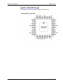
ispPAC Pinout Reference
105
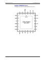
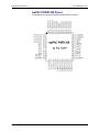
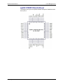
Power Manager Pinout 105
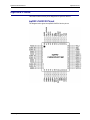
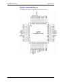
ispPAC-POWR604 Pinout 105
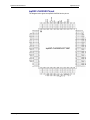
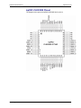
ispPAC-POWR605 Pinout 107
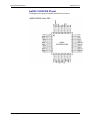
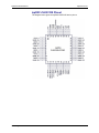
ispPAC-POWR607 Pinout 108
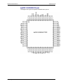
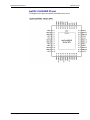
ispPAC-POWR1208 Pinout 109
ispPAC-POWR1208P1 Pinout 110
ispPAC-POWR1220AT8(-02) Pinout 111
ispPAC-POWR1014(-02) Pinout 112
ispPAC-POWR1014A(-02) Pinout 113
LA-ispPAC-POWR1014 Pinout 114
LA-ispPAC-POWR1014A Pinout 115
ispPAC-POWR6AT6 Pinout 116
Platform Manager Pinout
116
ispClock Pinout 123
ispPAC-CLK5510 Pinout
ispPAC-CLK5520 Pinout
ispPAC-CLK5610 Pinout
ispPAC-CLK5620 Pinout
ispPAC-CLK5610A Pinout
ispPAC-CLK5620A Pinout
ispPAC-CLK5304S Pinout
ispPAC-CLK5308S Pinout
ispPAC-CLK5312S Pinout
PAC-Designer Software User Manual
123
124
125
126
127
128
129
130
131
vii
Contents
ispPAC-CLK5316S Pinout 132
ispPAC-CLK5320S Pinout 133
ispPAC-CLK5406D Pinout 134
ispPAC-CLK5410D Pinout 135
Device Programming
137
Download Cable Overview
138
Download Cable Specifications
Error Messages
139
About UES Bits
141
139
Procedures 141
Installing the PACJTAG.SYS Device Driver (WinNT/2000)
Setting JTAG Interface Options 142
Testing the Parallel Port Connection 142
Setting Security Options 143
Setting UES Bits in an ispPAC Device 143
Downloading Schematic Data to a Device 144
Uploading Data from a Device to a Schematic 144
Verifying a Device Schematic 144
Performing Auto-Calibrate on a Device 144
Power Manager Example Implementation
141
145
Design Example Implementation Steps 145
Creating/Opening a Design File
Configuring Analog Inputs
Configuring Digital Inputs
147
150
153
Configuring Digital Outputs
155
Configuring HVOUT Pins (MOSFET Driver Pins) 157
Configuring Timers
159
Implementing Power Management Algorithm in LogiBuilder
162
LogiBuilder - Sequence Control 163
Entering a Program into the Sequence Controller 164
Sequencer Instructions 164
LogiBuilder - Exception Conditions 183
Creating an Exception Condition 184
LogiBuilder - Supervisory Logic
187
Digital Timing Simulation Using PAC-Designer
Implementing Multiple State Machines
196
Creating a DC-DC Converter Library Entry
Recommended References
Index
PAC-Designer Software User Manual
192
198
211
213
viii
1
Introduction to PACDesigner
PAC-DesignerTM is the complete design environment for Lattice
Semiconductor Power Manager, Platform Manager, and ispClock. PACDesigner permits real-time design of analog circuits using the Lattice ispPAC
family of components. With PAC-Designer you can configure and interrogate
any of the ispPAC products using its intuitive point-and-click features.
Your design can be quickly downloaded to the device, where it is stored
permanently. Each ispPAC product includes proprietary on-chip circuitry to
store your design in its E2CMOS memory.
Design Examples Included with the software are many design examples
for Power Manager, Platform Manager, and ispClock devices. A brief
description of each example is included in the Design Examples dialog box,
which you can access from the File menu. More complete information is
available in the Design_Examples_PPT.pdf file located in the Examples folder
of the PAC-Designer installation directory.
Literature Much more information, including application notes and
development kits, is available from the Lattice website. See the
“Recommended References” on page 211 for a full list of these documents.
PAC-Designer Software User Manual
1
Introduction to PAC-Designer
General Capabilities of PAC-Designer
General Capabilities of PAC-Designer
Design iterations are quick and easy with PAC-Designer. Just change the
design schematic, compile the sequence logic, confirm the operation using a
design utility or simulator, and download to the device. Likewise, any part
which is not read-protected can be interrogated to reveal the stored
configuration.
Edit Multiple Designs
PAC-Designer can edit multiple designs at once. Each design is stored in a
separate file.
Hierarchical Design Entry
A schematic block-diagram allows easy access to configure each major
function of Power Manager, Platform Manager, and ispClock devices. The
block-diagram produces configuration data for the ispVM programming
interface.
ispClock Design Utilities
Frequency Calculator – Reads a configuration from PAC-Designer, and
calculates all output frequencies for a given reference input frequency.
Frequency Checker – Reads a configuration from PAC-Designer and decides
whether the operating frequencies of the phase detector and the VCO are
within rated limits.
Frequency Synthesizer – Calculates a device configuration that produces the
desired output frequencies based on input and output frequency.
Skew Editor – Provides a graphical interface for configuring the relative edge
skews of device outputs.
Power Manager/Platform Manager Design Utilities
HVOUT Simulator – Simulates the rise time of a power supply driven by an NChannel MOSFET and the HVOUT drivers of a Power Manager or Platform
Manager device.
I2C Utility – Drives I2C interfaces with the Lattice ispDownload Cable.
PAC-Designer Software User Manual
2
Introduction to PAC-Designer
Starting PAC-Designer
LogiBuilder Design Entry
A tabular user interface for creating Power Manager PLD core power supply
sequence controller logic based on conditional events and timer delays.
LogiBuilder produces ABEL-HDL source files.
Functional Simulator
A logic simulator for the digital logic targeted to the Power Manager or
Platform Manager PLD core.
Waveform Editor
A graphical editor for creating digital test patterns for the Power Manager or
Platform Manager PLD core simulator. The Waveform Editor produces
Waveform Description Language (WDL) source files.
Starting PAC-Designer
The procedure for starting and exiting PAC-Designer is the same as for other
Windows-based applications.
To start PAC-Designer:
From the Windows Start menu button, choose
Programs > Lattice PAC-Designer > PAC-Designer.
To exit PAC-Designer:
choose File > Exit.
Process Flow
Here is a quick look at the PAC-Designer process flow.
ispClock
1. Configure ispClock functions by editing the schematic.
2. Confirm clock functions using the ispClock design utilities.
3. Download the design to the device connected to the PC parallel port. The
ispClock devices use an IEEE1149.1 (JTAG boundary-scan)-compliant
serial interface.
Power Manager
1. Configure Power Manager functions by editing the schematic.
2. Design and simulate PLD core logic with LogiBuilder and the simulator.
3. Confirm power supply rise time using the HVOUT simulator design utility.
4. Download the design to the device connected to the PC parallel port.
Power Manager devices use an IEEE1149.1 (JTAG boundary-scan)compliant serial interface.
PAC-Designer Software User Manual
3
Introduction to PAC-Designer
Exporting/Importing Data
Exporting/Importing Data
PAC-Designer can export alternative forms of schematic and plot data. This
information can be used for design documentation, importing into third-party
software such as a spreadsheet for graphing, or as in the case of .svf file
(JTAG serial vector format), data to program or read from devices in a JTAG
serial chain.
PAC-Designer supports several types of data which may be exported or
imported in several formats. The data types supported by PAC-Designer for
export/import are device dependent.
Data
Exported As...
Import
Export
Schematic
JEDEC File
Yes
Yes
Serial Vector Format
No
Yes
Formatted Text
No
Yes
SPICE Netlist
No
Yes
LogiBuilder PAC File
Yes
Yes
Margin/Trim PAC File
Yes
Yes
Formatted Text
Yes
Yes
Plot Data
For Power Manager and Platform Manager devices, you can also export
digital elements (timers and the PLD core) to a Verilog or VHDL file for
functional simulation. See Simulating a Power Manager Design with Aldec
Active-HDL for details.
PAC-Designer Software User Manual
4
2
ispPAC Device Summary
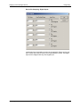
Table 1: ispPAC Device Summary
Device
Applications
ispPAC-POWR604
Power supply monitoring
8-macrocell PLD
Power supply start-up/shutdown sequencing
2 programmable timers
On-chip clock generator
6 programmable threshold comparators
4 open-drain digital outputs
4 digital inputs
ispPAC-POWR605
Features
Power supply monitoring
16-macrocell PLD
Power supply start-up/shutdown sequencing
4 programmable timers
On-chip clock generator
6 programmable threshold comparators
2 digital inputs
5 digital pins that can be configured as inputs or
open drain outputs
Low ICC power-down mode
PAC-Designer Software User Manual
5
ispPAC Device Summary
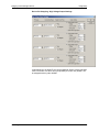
Table 1: ispPAC Device Summary (Continued)
Device
Applications
Features
ispPAC-POWR607
Power supply monitoring
16-macrocell PLD
Power supply start-up/shutdown sequencing
4 programmable timers
On-chip clock generator
6 programmable threshold comparators
2 high-voltage FET driver outputs
2 digital inputs
5 digital pins that can be configured as inputs or
open drain outputs
Low ICC power-down mode
ispPAC-POWR1208/
Power supply monitoring
16-macrocell PLD
ispPAC-POWR1208P1
Power supply start-up/shutdown sequencing
4 programmable timers
On-chip clock generator
12 programmable threshold comparators
4 high-voltage FET driver outputs
4 open-drain digital outputs
4 digital inputs
ispPACPOWR1220AT8(-02)
ispPAC-POWR1014(-02)
Power supply monitoring
48-macrocell PLD
Power supply start-up/shutdown sequencing
4 programmable timers
On-chip clock generator
24 programmable threshold comparators with
window (12 VMON pins)
4 high-voltage FET driver outputs
16 open-drain digital outputs
6 digital inputs
Trim and margin with DACs
I2C A/D and control interface
Power supply monitoring
24-macrocell PLD
Power supply start-up/shutdown sequencing
4 programmable timers
On-chip clock generator
20 programmable threshold comparators with
window (10 VMON pins)
2 high-voltage FET driver outputs
12 open-drain digital outputs
4 digital inputs
PAC-Designer Software User Manual
6
ispPAC Device Summary
Table 1: ispPAC Device Summary (Continued)
Device
Applications
Features
ispPAC-POWR1014A(02)
Power supply monitoring
24-macrocell PLD
Power supply start-up/shutdown sequencing
4 programmable timers
On-chip clock generator
I2C A/D and control interface
20 programmable threshold comparators with
window (10 VMON pins)
2 high-voltage FET driver outputs
12 open-drain digital outputs
4 digital inputs
LA-ispPAC-POWR1014
Power supply monitoring
24-macrocell PLD
(Automotive Grade)
Power supply start-up/shutdown sequencing
4 programmable timers
On-chip clock generator
20 programmable threshold comparators with
window (10 VMON pins)
2 high-voltage FET driver outputs
12 open-drain digital outputs
4 digital inputs
LA-ispPAC-POWR1014A
Power supply monitoring
24-macrocell PLD
(Automotive Grade)
Power supply start-up/shutdown sequencing
4 programmable timers
On-chip clock generator
I2C A/D and control interface
20 programmable threshold comparators with
window (10 VMON pins)
2 high-voltage FET driver outputs
12 open-drain digital outputs
4 digital inputs
ispPAC-POWR6AT6
Power supply trim and margin
Closed loop trim control
Power supply monitor and
control
Static trim settings
I2C interface
Differential VMON sense lines
10 bit ADC
8 bit trim DACs
ispPAC-CLK5510/
Precision clock generator
10-320 MHz output
ispPAC-CLK5520
Frequency multiplication &
division
Low cycle-to-cycle and period jitter
Programmable input and output termination
Supports LVCMOS, LVTTL, LVPECL, LVDS,
HSTL, and SSTL standards
E2CMOS memory stores up to four userselectable profiles
Independently programmable skew and slew rate
control on each output
PAC-Designer Software User Manual
7
ispPAC Device Summary
Table 1: ispPAC Device Summary (Continued)
Device
Applications
ispPAC-CLK5610/
Precision clock generator
10-320MHz output
ispPAC-CLK5620
Frequency multiplication &
division
Low cycle-to-cycle and period jitter
Programmable input and output termination
Zero-delay buffer
Supports LVCMOS, LVTTL, LVPECL, LVDS,
HSTL, and SSTL standards
E2CMOS memory stores up to four userselectable profiles
Independently programmable skew and slew rate
control on each output
4-400MHz output
Low cycle-to-cycle, period and phase jitter
Programmable input and output termination
Supports LVCMOS, LVTTL, LVPECL, LVDS,
HSTL, SSTL, differential HSTL and differential
SSTL standards
E2CMOS memory stores up to four userselectable profiles
Independently programmable skew and slew rate
control on each output
8MHz to 267MHz
Low cycle-to-cycle, period and phase jitter
Programmable input and output termination
Supports input standards: LVCMOS, LVTTL
LVPECL, LVDS, HSTL, SSTL, differential HSTL
and differential SSTL standards
E2CMOS memory stores up to four userselectable profiles
Independently programmable skew and slew rate
control on each output
ispPAC-CLK5610A/
Enhanced zero delay clock
generator
Frequency multiplication &
division
Zero-delay buffer
ispPAC-CLK5620A
ispPAC-CLK5304S
ispPAC-CLK5308S
Zero delay universal fan-out
buffer
4 single-ended outputs
Frequency multiplication &
division
Zero-delay buffer
Zero delay universal fan-out
buffer
8 single-ended outputs
Frequency multiplication &
division
Zero-delay buffer
PAC-Designer Software User Manual
Features
8
ispPAC Device Summary
Table 1: ispPAC Device Summary (Continued)
Device
Applications
ispPAC-CLK5312S
Zero delay universal fan-out
buffer
12 single-ended outputs
Frequency multiplication &
division
Zero-delay buffer
ispPAC-CLK5316S
ispPAC-CLK5320S
ispPAC-CLK5406D
Zero delay universal fan-out
buffer
16 single-ended outputs
Frequency multiplication &
division
Zero-delay buffer
Zero delay universal fan-out
buffer
20 single-ended outputs
Frequency multiplication &
division
Zero-delay buffer
Differential zero delay
universal fan-out buffer
6 differential outputs
Frequency multiplication &
division
Zero-delay buffer
PAC-Designer Software User Manual
Features
8MHz to 267MHz
Low cycle-to-cycle, period and phase jitter
Programmable input and output termination
Supports input standards: LVCMOS, LVTTL
LVPECL, LVDS, HSTL, SSTL, differential HSTL
and differential SSTL standards
E2CMOS memory stores up to four userselectable profiles
Independently programmable skew and slew rate
control on each output
50MHz to 400MHz
Low cycle-to-cycle, period and phase jitter
Programmable input and output termination
Supports differential standards: LVPECL, LVDS,
MLVDS, HSTL, SSTL
Independently programmable skew
9
ispPAC Device Summary
Table 1: ispPAC Device Summary (Continued)
Device
Applications
ispPAC-CLK5410D
Differential zero delay
universal fan-out buffer
10 differential outputs
Frequency multiplication &
division
Zero-delay buffer
Platform Manager
(LPTM10-1247 &
LPTM10-12107)
Features
50MHz to 400MHz
Low cycle-to-cycle, period and phase jitter
Programmable input and output termination
Supports differential standards: LVPECL, LVDS,
MLVDS, HSTL, SSTL
Independently programmable skew
Hot-swap controller
48-macrocell PLD
Power supply OR’ing
4 programmable timers
Voltage monitoring
On-chip clock generator
Sequence control
Trimming & margining
24 programmable threshold comparators with
window (12 VMON pins)
Power-on configuration
4 high-voltage FET driver outputs
Reset distribution
12 open-drain digital outputs
Fault logging
4 digital inputs
8 Margin/Trim outputs
91 digital I/O's
640 LUT FPGA
System interface
PAC-Designer Software User Manual
10
3
Designing Power Manager
Devices
This section illustrates Power Manager designs. It includes six sub-sections:
Design Entry
LogiBuilder
Functional Logic Simulation
Automatic ABEL Import Waveform Editor
Waveform Editor (Stimulus)
Waveform Viewer (Results)
Design Entry
This section contains concepts and procedures for designing Power Manager
devices.
Concepts
This section describes Power Manager design concepts.
Schematic Entry
Schematic entry consists of making internal connections and choosing
parametric circuit values on an ispPAC device schematic window. When
complete, the circuit can be simulated, saved, or downloaded to an ispPAC
device. As an alternative to complete configuration, standard circuit functions
are available from a library of stored designs.
The PAC-Designer schematic window provides access to all configurable
ispPAC device elements through its graphical user interface. All input and
output pins are represented. Static or non-configurable pins such as power,
PAC-Designer Software User Manual
11
Designing Power Manager Devices
Design Entry
ground, VREF OUT and the serial digital interface are purposely omitted. Any
element in the schematic window can be accessed through mouse operations
as well as by menu commands.
Schematic Entry - Power Manager Devices
The PAC-Designer schematic window provides access to all configurable
Power Manager device elements through its graphical user interface. All input
and output pins are represented. Some of the non-configurable pins such as
the serial digital interface are purposely omitted. Any element in the
schematic window can be accessed through mouse operations as well as by
menu commands.
The schematic for the Power Manager device is hierarchical as it contains
other schematic or text entry windows within a given block. These blocks are
edited by double-clicking a given section. You can navigate between the
different blocks with simple click and edit features.
Power Manager Design Utilities
There are two design utilities available for the Power Manager devices:
Power Manager HVOUT Simulator – Allows you to simulate the rise time
of a power supply driven by an N-Channel MOSFET and the HVOUT
drivers on the Power Manager devices.
Power Manager I2C Utility (I2C capable devices only) – Allows you to
drive the I2C interface with the Lattice ispDownload Cable.
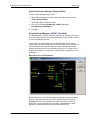
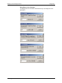
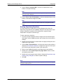
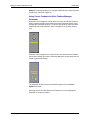
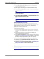
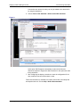
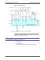
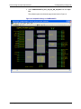
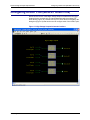
Trimming and Margining Power Supplies
Setting up the trim and margin capabilities of ispPAC-POWR1220AT8 and
ispPAC-POWR6AT6 involves two different tools within PAC-Designer. The
DC-DC Library Builder is used to define the voltage adjustment
characteristics of the power supply or supplies that you wish to use. The Trim
Configuration Dialog Box is then used to configure each trim channel for the
desired power supplies and output voltages. This arrangement provides the
convenience of being able to re-use a single power supply in several different
trim channels or projects without having to re-enter its parameters each time.
The flow is illustrated below:
PAC-Designer Software User Manual
12
Designing Power Manager Devices
Design Entry
Modifications to existing DC/DC library files must be made from within the DC/
DC Library Builder. Changes in the desired target voltages or supply selection
are done from the Trim Configuration dialog box. It is strongly advised that
library files not be modified while trim cells are being configured because this
can create confusion and make it difficult to detect errors in your work. If a
“discrete” supply is to be used at several different voltages, a separate library
entry for each unique output voltage should be created.
The Library Builder stores its files in the “DCtoDC_Library” directory, which is
located under the main PAC-Designer install directory. The Trim Configuration
dialog box import facility launches a file browser in order to make it possible to
import library files created in earlier versions of PAC-Designer or library files
that have been stored elsewhere.
The Trim Configuration dialog box provides the ability to re-do the trim
calculations with a minimum amount of parameter re-entry. Target voltages
need to be re-entered only if the desired supply type is changed.
Reserved Words
None of these words should be used as a pin name in PAC-Designer:
Async_reset
Case
Clk_in
Declarations
Device
Else
Enable
End
Endcase
Equations
External
Flag
Functional_block
Fuses
Goto
If
In
Interface
Istype
Library
Macro
Module
Node
Options
Pin
Pld_clk
Property
Reset
State
State_diagram
State_register
Sync_reset
PAC-Designer Software User Manual
13
Designing Power Manager Devices
Design Entry
Tmr_clk
Test_vectors
Then
Title
Trace
Truth_table
When
With
Invalid Characters
Do not use any of the following characters in a name.
!@#$%^&*()+=/><{}:;~
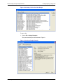
Design Examples
The PAC-Designer software provides a library of pre-configured designs for
example use. Choose File > Design Examples. The Design Examples
Dialog Box contains a list of pre-configured designs. When you click a design
in the list, a description of the design appears on the right side of the dialog
box.
You can open the schematic, and use it as-is, or you can edit the schematic.
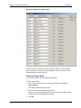
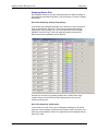
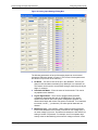
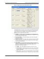
Design Mapping Table
The following table shows mapping details for importing an ispPACPOWR1014/A design into an ispPAC-POWR1220AT8 device.
Table 1: Design Mapping
Source Device: ispPAC-POWR1014/A
Target Device: ispPAC-POWR1220AT8
VMON 1 to 10 pins
Mapped to VMON 1 to 10 of ispPAC-POWR1220AT8
Thresholds (coarse and fine settings)
The actual threshold voltage in the target device may be shifted by a
few mill volts
Pin names
Same pin names as source
Logical names
Same logical names as source
Glitch filter setting per pin
Same glitch filter setting per pin as source
Window comparator setting
Same window comparator setting as source
Input 1 to 4 pins
Mapped to IN1 to 4 of ispPAC-POWR1220AT8
Pin names
Same pin names as source
JTAG control bit setting
Same JTAG control bit setting for IN1 pin as source
I2C setting (ispPAC-POWR1014A only)
Same I2C setting for IN2 to 4 as source
I2C address (ispPAC-POWR1014A only)
Same I2C address as source
Timers 1- 4
Same Timers 1-4 setting as source
MCLK & PLD clock setting
MCLK and PLD clock setting
PAC-Designer Software User Manual
14
Designing Power Manager Devices
Design Entry
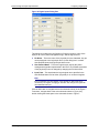
Table 1: Design Mapping (Continued)
Source Device: ispPAC-POWR1014/A
Target Device: ispPAC-POWR1220AT8
Output 3 to 14
Mapped to output 5-16 of ispPAC-POWR1220AT8
Output pin names
Same output pin names as source
I2C control setting of the output pin
Same I2C control setting of the output pin as source
SMBAlert setting
Same SMBAlert setting as source
HVOUT 1-2
Mapped to HVOUT 1-2 of ispPAC-POWR1220AT8
Output type - charge pump / digital output
Output type - charge pump / digital output setting maintained
HVOUT output voltage setting
HVOUT output voltage setting maintained
HVOUT source current setting
HVOUT source current setting maintained
HVOUT sink current setting
HVOUT sink current setting maintained
Entire LogiBuilder program
Mapped to entire LogiBuilder program of ispPAC-POWR1220AT8
Procedures
This section provides step-by-step procedures for completing tasks you can
perform in designing Power Manager designs.
Creating a New Schematic
You can create a new schematic, or open an existing schematic.
To create a new schematic:
1. Choose File > New.
The New Dialog Box opens.
2. Select the schematic for the ispPAC device you wish to design.
3. Click OK.
The device schematic window is displayed.
Editing a Schematic
You can edit a schematic using several techniques, including:
Double-Click
You can double-click over each symbol in the Schematic Window to invoke
the appropriate dialog box to edit the item. See Editing Schematic Symbols.
Click and Drag to Connect wires
Feedback – Drag from the point furthest from the resistor to close the
connection
IA Inputs – Drag from Instrumentation Amp input to an input or output
terminal wire
PAC-Designer Software User Manual
15
Designing Power Manager Devices
Design Entry
Disconnect wires – Connections can be opened by dragging the wire back
to its starting point.
Menu Entry
Choose Edit > Symbol.
The Edit Symbol dialog box opens. This shows a list of all symbols seen
on the schematic.
To edit a symbol, double-click the desired symbol on the list and choose
the Edit button;
or
Select the symbol from the list and press Enter.
A secondary dialog box specific to the symbol will appear.
Zoom
Use standard Windows-style zoom.
Editing Schematic Symbols
PAC schematics contain SPST and SPMT switches, and components. This
topic describes how to edit them. Cursor feedback provides visual cues to aid
the editing.
Symbols are also known by name, and can be edited by name.
Single-Throw switch (feedback resistor)
To Close: Drag from active contact (indicated by cursor) to close the
connection.
To Open: Drag from active contact (indicated by cursor) to open the
connection.
Edit Dialog Box: Double-click over active area (indicated by cursor).
Multiple-Throw switch (Interconnect to Input Stage)
To Close: Drag from Input Stage input to an terminal wire (indicated by
cursor).
To Open: Drag from connected terminal wire back to Input Stage input.
Edit Dialog Box: Double-click over active area (indicated by cursor).
PAC-Designer Software User Manual
16
Designing Power Manager Devices
Design Entry
Circuit components (caps, input stage gain, and so on)
Edit Dialog Box: Double-click over active area (indicated by cursor).
Editing a Power Manager Schematic
The Power Manager device main schematic contains function blocks that can
be edited by double-clicking any given block.
Analog Inputs: The Analog Inputs are comparator inputs, each with a
programmable threshold trip point, the outputs of the comparators feed into
the CPLD of the Sequencer Block.
Digital Inputs: The Digital Inputs are general purpose inputs for the logic. The
voltage thresholds can be set for lower voltage logic using the VDDinp pin.
Logic Outputs: The Logic Outputs are open-drain outputs that come from the
CPLD.
General Purpose I/O Pins (ispPAC-POWR607 only): Five pins on the device
can be individually configured to behave as either digital inputs or open drain
logic outputs. The mode setting for each pin is stored in non-volatile memory.
When one of these pins is used as an input, the open drain output circuit is
disabled. On the other hand, when one of these pins is used as an output, the
feedback for that pin's macrocell is taken from the output routing pool, rather
than the pin.
High Voltage Outputs: The HVOUT pins can be used as FET gate drivers
and have a programmable drive levels for both voltage and current. The
HVOUTs can also be set independently, to be used as digital outputs in opendrain mode.
Timer and Oscillator: The Timer and Oscillator functions are programmable.
The hardware timers can be programmed for different time delays.
Clock and Timers (ispPAC-POWR607 only): Four programmable timers can
be set, independently, to a wide variety of durations in the range of 32s to
1.966s.
Sequence Controller: The Sequence Controller Block is the section
supported by the CPLD. The editing within this block is done with LogiBuilder,
a built-in utility of PAC-Designer.
Comparator Buffer (ispPAC-POWR604 and ispPAC-POWR1208/P1 only):
The COMP BUFF block represents the outputs of the comparators and serve
as expansion to drive other circuits.
Vmon Inputs & ADC (ispPAC-POWR6AT6 only): The Vmon Inputs and
Analog-to-Digital Converter (ADC) inputs are the analog front-end of the
PAC-Designer Software User Manual
17
Designing Power Manager Devices
Design Entry
device. The values read by the ADC are used by the closed loop trim control
logic and may be read at any time through I2C. No user-programmable
settings are contained in these blocks of the schematic window.
Control Logic (ispPAC-POWR6AT6 only): This block represents the circuitry
that makes closed loop trimming possible. Double-clicking the block allows
the closed loop trim DAC update time to be set.
I2C (ispPAC-POWR6AT6 only): This block allows configuration of the devices
I2C and SMBUS capabilities.
Trim Cell 1-6 (ispPAC-POWR6AT6 only): These blocks allow each trim cell to
be configured by inputting the desired supply output voltages, selecting power
supplies from the DC-DC library, and setting the trim cells modes of operation.
When all of these parameters have been entered, the bottom part of this
dialog box displays the resistor values needed to interface the Trim Cell
Digital-to-Analog Converter (ADC) to the power supply.
UES: The UES is for storing user-defined information such as board revision
or code revision. There are 16 bits accessible to you. The bits are nonvolatile.
Margin and Trim Block (ispPAC-POWR1220AT8 only): The Margin/Trim
Block sets up all the modes for the trim circuitry to adjust DC/DC power
supplies. It allows control of all the DAC settings and modes for margining and
trimming.
I2C Control Block (ispPAC-POWR1014A only): This block allows you to set
several modes for the device pins and the I2C address.
Using Cursor Feedback to Edit a Power Manager Schematic
When the cursor changes to a down arrow, the block can be pushed into for
editing. Double-clicking a block within the top-level schematic allows you to
navigate the schematic hierarchy. To return to the top-level, place the cursor
towards the top of the schematic, when it changes to an up arrow, doubleclick.
When the cursor changes over a given block to the edit arrow with brackets,
then double-clicking will invoke a secondary dialog box for text entry such as
a table or parameter change.
PAC-Designer Software User Manual
18
Designing Power Manager Devices
Design Entry
The schematic blocks can also be edited through the use of the Edit >
Symbol command.
Selecting an item from the dialog box will transfer you to the appropriate
schematic or window for editing.
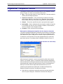
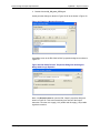
Swapping Device Pins
PAC-Designer allows you to swap external physical pins while the design is
being worked on and still being edited. This can be done to correct or simplify
board layout.
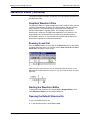
Device Pin Swapping - Analog Input Settings
In the Analog Input Settings dialog box, the external pin names are listed in
the first column under “Pin Name.” These names represent the physical
external pins of the package. You can use the pull-down menus to swap
VMONs in this first column. This only swaps the physical external pins.
Names used inside LogiBuilder are not affected.
PAC-Designer Software User Manual
19
Designing Power Manager Devices
Design Entry
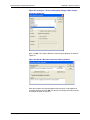
External pins can also be physically swapped in the Digital Inputs, High
Voltage Output Settings, and Logic Outputs dialog boxes.
PAC-Designer Software User Manual
20
Designing Power Manager Devices
Design Entry
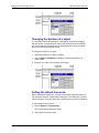
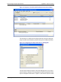
Device Pin Swapping - Digital Inputs
In this dialog box, the digital input pins can be swapped. Simply use the pulldown menus and make sure there are no duplicated pin names. Any digital
input can be swapped with any other digital input.
PAC-Designer Software User Manual
21
Designing Power Manager Devices
Design Entry
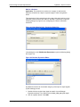
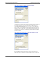
Device Pin Swapping - High Voltage Output Settings
In this dialog box, the HVOUT pins can be swapped. Simply use the pull-down
menus and make sure there are no duplicated pin names. Any HVOUT can
be swapped with any other HVOUT.
PAC-Designer Software User Manual
22
Designing Power Manager Devices
Design Entry
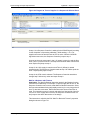
Device Pin Swapping - Logic Outputs
In this dialog box, the OUT pins can be swapped. Simply use the pull-down
menus and make sure there are no duplicated pin names. Any OUT pin can
be swapped with any other OUT pin.
Starting a Design Utility
You can use a design utility to modify your schematic.
To start a design utility:
1. With a device schematic open in the Main Window, choose Tools >
Design Utilities.
The Design Utilities dialog box opens.
2. From the list, select the desired design utility.
When a selection is highlighted in the list, a description of the design utility
is displayed in the Design Utilities dialog box.
3. Click OK.
PAC-Designer Software User Manual
23
Designing Power Manager Devices
Design Entry
Starting the Power Manager Design Utilities
To start a Power Manager design utility:
1. With a Power Manager schematic open in the Main Window, choose
Tools > Design Utilities.
The Design Utilities dialog box opens.
2. From the list, select PowerManager_HVOUT_Sim.exe or
PowerManager_I2CUtility.exe.
3. Click OK.
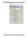
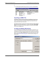
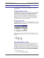
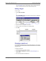
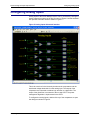
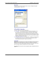
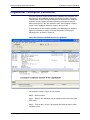
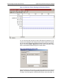
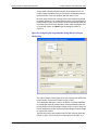
Using the PowerManager_HVOUT_Sim Utility
The PowerManager_HVOUT_Sim Utility allows you to simulate the rise time
of a power supply driven by an N-Channel MOSFET and the HVOUT drivers
on the Power Manager devices.
This simulator uses parameters from the MOSFET data sheet to build a
model, the circuit is then simulated based on inputs from the user interface. To
edit any values on the schematic within the utility, simply double-click the
different circuit elements on the schematic such as the FET, HVOUT block,
resistors and capacitor. This will open up dialog boxes to change the circuit
parameters.
Main Screen for the FET Simulator
Double-clicking the circuit elements within the schematic will bring up dialog
boxes for each parameter. Once you have configured the set up, hit the
Simulate button and the results will be plotted. The results can also be
exported to a coma-separated file to be used in a spreadsheet for other
analysis or comparing different ramp rates with different FETs.
PAC-Designer Software User Manual
24
Designing Power Manager Devices
Design Entry
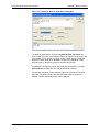
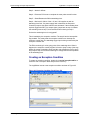
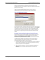
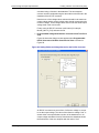
Dialog Boxes for the Simulator
The dialog boxes for the HVOUT Simulator allow you to change the circuit
parameters.
PAC-Designer Software User Manual
25
Designing Power Manager Devices
Design Entry
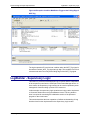
MOSFET Library
The MOSFET library holds the model for the FETs. You can modify the
parameters for the FETs and these are stored in the library for later use.
PAC-Designer Software User Manual
26
Designing Power Manager Devices
Design Entry
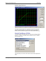
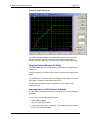
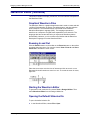
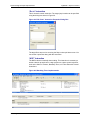
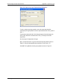
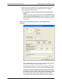
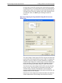
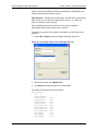
Simulation Output Plot Screen
The results are plotted based on the parameters entered. The actual data
points can then be exported to a .csv file to be used in a spreadsheet if
needed. The Plot window also supports cursor measurements and printing.
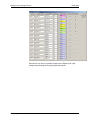
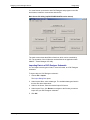
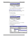
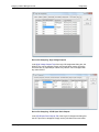
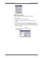
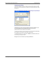
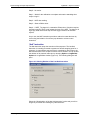
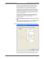
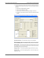
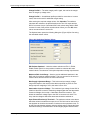
Using the PowerManager_I2CUtility
The Power Manager I2C design utilities are opened from the Design Utilities
dialog box. A separate I2C software utility is available for each I2C capable
Power Manager Device.
This utility allows you to drive the I2C interface with the Lattice ispDownload
Cable.
PAC-Designer Software User Manual
27
Designing Power Manager Devices
Design Entry
You must first set up the device with PAC-Designer and program in the I/Os
and features needed to communicate with the I2C.
Main Screen I2C Utility (ispPAC-POWR1220AT8 version shown)
The main screen shows the different functions, which can be controlled by
I2C. The operation of the full features are described in an Application Note:
AN6067 – Power Manager I2C Utility.
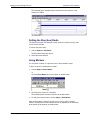
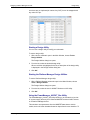
Importing Data to a PAC-Designer Schematic
You can import several types of data, in several formats, to a PAC-Designer
schematic.
To import data to a PAC-Designer schematic:
1. Choose File > Import.
The Import Dialog Box opens.
2. Under Import What, select a data type. The available data types listed in
this box are device-dependent.
3. Under In the format, select the desired import file format.
4. Under Import From, click Browse to navigate to the file that you want to
import into your PAC-Designer schematic.
5. Click OK.
PAC-Designer Software User Manual
28
Designing Power Manager Devices
Design Entry
Exporting Data from a PAC-Designer Schematic
You can export several types of data, in several formats, from a PAC-Designer
schematic.
For Power Manager devices, you can also export digital elements (timers and
the PLD core) to a Verilog or VHDL file for functional simulation. See
Simulating a Power Manager Design with Aldec Active-HDL for details.
To export data from a PAC-Designer schematic:
1. Choose File > Export.
The Export Dialog Box opens.
2. Under Export What, select a data type. The available data types listed in
this box are device-dependent.
3. Under In this format, select the desired export file format.
4. If you want to export the data to a file, select File, and then click Browse
to navigate to the file to which you want to export data.
5. If you want to export the data to your computers Clipboard memory, select
Clipboard.
6. Click OK.
Creating and Editing an ABEL Design
You can create and edit an ABEL design for a Power Manager device.
To create and edit an ABEL design:
1. From the top level schematic window, configure the user-defined inputs
and outputs, set the VMON trip points, and configure the clock and timer
settings.
2. Double-click the Sequence Controller block to display the Sequence and
Supervisory Logic Window.
3. Choose View > Pins definitions, or click the pins button on the toolbar, to
display the Pin Definitions Window to configure the logic level of the input
pins; and the type and power-up state of the output pins.
4. Return to the LogiBuilder Sequence and Supervisory Logic Window and
enter a minimal sequence using the timers and outputs you plan to use in
ABEL.
5. Choose Tools > Compile LogiBuilder Design, or click the compile
button on the toolbar, to generate an ABEL template from which your
custom ABEL design can be built from.
6. Choose View > ABEL Source to open an ABEL Source Window.
7. Choose Edit > Enable ABEL Editing to enable the edit window and
disable the LogiBuilder window.
8. Make changes to the ABEL source to implement the desired design.
PAC-Designer Software User Manual
29
Designing Power Manager Devices
Design Entry
9. Choose Tools > Compile ABEL, or click the compile button on the
toolbar, to compile the design.
Note
If syntactical or other ABEL errors are in the design, the compilation will fail and an
error report will be displayed.
10. Choose Tools > Run PLD Simulator, or click the simulator button on the
toolbar, to simulate the design from ABEL.
Note
The default stimulus file should be edited to reflect the input signals and basic
design.
Entering Supervisory Equations
You enter supervisory equations for a Power Manager device from the
Supervisory Logic panel of the LogiBuilder Sequence and Supervisory Logic
window. Supervisory equations are combinatorial or registered logic
independent of sequence controller logic.
To enter supervisory equations:
1. From the top level schematic window, configure the user-defined inputs
and outputs, set the VMON trip points, and configure the clock and timer
settings.
2. Double-click the Sequence Controller block to display the Sequence and
Supervisory Logic window.
3. Choose View > Pins definitions, or click the pins button on the toolbar, to
display the Pin Definitions Window to configure the logic level of the input
pins; and the type and power-up state of the output pins.
4. Return to the LogiBuilder Sequence and Supervisory Logic window.
5. Double-click on the <end-of-supervisory-logic-table> marker to insert
an equation place holder.
6. Double-click on the equation place holder to display the Supervisory Logic
Equation Entry Dialog Box to edit the equation settings.
7. Click OK.
Note
LogiBuilder sequencing, exceptions, and supervisory equations are combined together
during the compile process.
PAC-Designer Software User Manual
30
Designing Power Manager Devices
LogiBuilder
LogiBuilder
LogiBuilder is a utility within PAC-Designer software that allows you to define
a power supply sequence controller and monitor or other control circuits using
the Power Manager devices. The tools within the LogiBuilder include a set of
instructions to build the sequence based on conditional events and timer
delays. The overall entry simplifies the design process to menu selections as
opposed to writing complex code. Once the set of instructions are entered,
the user compiles the design and can simulate the sequence or control
events.
Three types of expression styles are provided to ease the definition of logic
and produce the most compact implementation in the Power Manager device:
Sequencer Instructions – Defines a step-by-step instruction for
controlling Power Manager outputs. When compiled, sequencer
instructions implement a digital logic state machine within the Power
Manager’s PLD core.
Exceptions – Define equations that will trigger sequence controller
exceptions to modify outputs and jump out to an alternative sequence
step. Exceptions can be selectively applied to any sequencer step. When
compiled, exception instructions are merged with the digital logic state
machine of the Power Manager’s PLD core.
Supervisory Equations – Define combinatorial and registered logic
independent of the sequencer control logic. When compiled, supervisory
equations are concurrent to the digital logic state machine of the Power
Manager’s PLD core.
PAC-Designer Software User Manual
31
Designing Power Manager Devices
LogiBuilder
LogiBuilder Sequence Controller Instruction Set
LogiBuilder provides the following instructions for designing control
sequences:
START STARTUP SEQUENCE
The START STARTUP SEQUENCE instruction signals to LogiBuilder that any
instructions past this point may be interrupted by jumps specified in
exceptions. This instruction may be deleted from a sequence, but not
inserted. Exceptions are automatically enabled following this point.
OUTPUT
The OUTPUT instruction is used to turn-on or turn-off the Power Manager
devices output signals. A single OUTPUT instruction can be used to
simultaneously change the status of any number of output signals.
WAIT FOR <Boolean Expression>
The WAIT FOR <Boolean expression> instruction suspends execution of the
sequence until the specified expression becomes TRUE.
WAIT FOR <Boolean Expression> with Timeout
The WAIT FOR <Boolean expression> with Timeout instruction suspends
execution of the sequence until the specified expression becomes TRUE or
the selected timer expires.
WAIT FOR <time> USING TIMER<1..4>
The WAIT FOR <time> instruction is used to specify a fixed delay in the
execution sequence. The value of <time> is determined by which timer
(TIMER1TIMER4) is specified.
IF <Boolean Expression> THEN GOTO <step x> ELSE GOTO <step y>
The IF-THEN-GOTO instruction provides the ability to modify sequence flow
depending on the state of inputs. If <Boolean expression> is TRUE, the next
step in the sequence will be <step x>, otherwise the next step will be <step
y>.
IF <Boolean Expression> THEN GOTO <step x> ELSE If Timer <n> GOTO
<step y> ELSE GOTO <step z>
This instruction provides the ability to modify sequence flow depending on the
state of inputs with an additional timeout feature. If <Boolean expression> is
TRUE, the next step in the sequence will be <step x>; otherwise, if Timer <n>
has expired, the next step will be <step y>. If <Boolean expression> is FALSE
and Timer <n> has not expired, then the next step will be <step z>. This
instruction only checks the values of <Boolean expression> and Timer <n>; it
does not start or reset the timer.
GOTO <step x>
The GOTO instruction forces the sequence to jump to <step x>
Start Timer
This instruction starts the selected timer. The status of the timer must be
checked using another instruction or combinational logic.
PAC-Designer Software User Manual
32
Designing Power Manager Devices
LogiBuilder
Stop Timer
This instruction stops and resets the selected timer.
NOP
The NOP instruction does not affect any of the outputs or the sequence of
execution. It is effectively a single-cycle delay.
HALT
The HALT instruction stops execution of the sequence.
BEGIN SHUTDOWN SEQUENCE
The BEGIN SHUTDOWN SEQUENCE instruction signals to LogiBuilder that
any instructions past this point will not be interrupted by jumps specified in
exceptions. This feature allows code used for handling exceptions not to be
interfered with by other exceptions that may occur. This instruction may be
deleted from a sequence, but not inserted.
Designing Control Sequences With LogiBuilder
The PAC-Designer LogiBuilder Sequence Controller window allows you to
create control sequences and define logic functions. When complete, the
circuit can be simulated, saved or downloaded to a Power Manager device.
To design a control sequence with LogiBuilder:
1. In a Power Manager Schematic Window, double-click the Sequence
Controller block to display the Sequence and Supervisory Logic window.
2. In the sequence (upper) portion of the window, highlight step 1, and
choose Edit > Insert Instruction to display the Insert Step Dialog Box.
3. In the dialog box, choose an instruction type, and click OK. Repeat as
necessary to add logic steps.
4. For each logic step, choose Edit > Modify Instruction Parameters to
display the appropriate Edit dialog box.
5. Select the desired logic properties in the Edit dialog box, and click OK.
6. To add exceptions, in the exceptions (lower) portion of the window,
highlight <end-of-exception-table>, and choose Edit > Add Exception.
Repeat as necessary to add exceptions.
7. For each exception, choose Edit > Modify Exception Parameters to
display the Exception Properties Dialog Box.
8. Select the desired exception properties, and click OK.
9. When the logic sequence is complete, compile your control sequence by
choosing Tools > Compile LogiBuilder Design.
PAC-Designer Software User Manual
33
Designing Power Manager Devices
LogiBuilder
Editing Pin Settings with LogiBuilder
Pin names are set at the schematic level. You can make edits to pin settings
with the Pin Definitions window.
To edit pin settings with LogiBuilder:
1. Choose View > Pin Definitions.
2. In the Pin Definitions Window, double-click the pin that you want to edit.
3. In the Pin Definition Dialog Box, make editable changes, and click OK.
Viewing Messages/Errors in LogiBuilder
You can view messages and errors in LogiBuilder.
To view messages and errors:
Choose View > Messages/Errors.
The Messages/Error Window opens.
Editing Multiple State Machines
The LogiBuilder supports multiple state machines for power up sequence and
control for some Power Manager devices. The state machines are defined
separately but can interact through nodes or common logic functions. Each
state machine is built up in a separate tab in the Sequence and Supervisory
Logic window. The logic for the full design is then compiled and fitted to
generate a single JEDEC file.
You can use the MSM Manager Dialog Box to add or delete state machines.
To open the dialog box, make sure the Sequence and Supervisory Logic
window is open, and the Sequencer Instructions table or the Exceptions table
is active, and then choose Edit > Multiple State Machines. Multiple state
machines are supported for the Sequencer Instructions table and the
Exceptions table only. The settings in the Supervisory Equations table always
apply to the entire design.
Creating and Editing an ABEL Design
You can create and edit an ABEL design for a Power Manager device.
To create and edit an ABEL design:
1. From the top level schematic window, configure the user-defined inputs
and outputs, set the VMON trip points, and configure the clock and timer
settings.
2. Double-click the Sequence Controller block to display the Sequence and
Supervisory Logic Window.
3. Choose View > Pins definitions, or click the pins button on the toolbar, to
display the Pin Definitions Window to configure the logic level of the input
pins; and the type and power-up state of the output pins.
PAC-Designer Software User Manual
34
Designing Power Manager Devices
LogiBuilder
4. Return to the LogiBuilder Sequence and Supervisory Logic Window and
enter a minimal sequence using the timers and outputs you plan to use in
ABEL.
5. Choose Tools > Compile LogiBuilder Design, or click the compile
button on the toolbar, to generate an ABEL template from which your
custom ABEL design can be built from.
6. Choose View > ABEL Source to open an ABEL Source Window.
7. Choose Edit > Enable ABEL Editing to enable the edit window and
disable the LogiBuilder window.
8. Make changes to the ABEL source to implement the desired design.
9. Choose Tools > Compile ABEL, or click the compile button on the
toolbar, to compile the design.
Note
If syntactical or other ABEL errors are in the design, the compilation will fail and an
error report will be displayed.
10. Choose Tools > Run PLD Simulator, or click the simulator button on the
toolbar, to simulate the design from ABEL.
Note
The default stimulus file should be edited to reflect the input signals and basic
design.
Entering Supervisory Equations
You enter supervisory equations for a Power Manager device from the
Supervisory Logic panel of the LogiBuilder Sequence and Supervisory Logic
window. Supervisory equations are combinatorial or registered logic
independent of sequence controller logic.
To enter supervisory equations:
1. From the top level schematic window, configure the user-defined inputs
and outputs, set the VMON trip points, and configure the clock and timer
settings.
2. Double-click the Sequence Controller block to display the Sequence and
Supervisory Logic window.
3. Choose View > Pins definitions, or click the pins button on the toolbar, to
display the Pin Definitions Window to configure the logic level of the input
pins; and the type and power-up state of the output pins.
4. Return to the LogiBuilder Sequence and Supervisory Logic window.
5. Double-click on the <end-of-supervisory-logic-table> marker to insert
an equation place holder.
6. Double-click on the equation place holder to display the Supervisory Logic
Equation Entry Dialog Box to edit the equation settings.
PAC-Designer Software User Manual
35
Designing Power Manager Devices
LogiBuilder
7. Click OK.
Note
LogiBuilder sequencing, exceptions, and supervisory equations are combined together
during the compile process.
LogiBuilder Error Messages
Error 0: Instruction at step “zero” cannot be a WaitFor_Timer or Start_Timer
instruction.
Reason: Timer_Gate signal must have a low-level then a high-level for timer
to operate. To do this for an instruction at step N, the instruction at step N-1
must set Timer_Gate=0, then Instruction N can set Timer_Gate=1. Therefore,
“N” cannot be zero.
Discussion: With the default LogiBuilder program template, you cannot get
this error because “Begin Startup Sequence” instruction is always present.
But users who choose to optimize code by removing the “Begin Startup
Sequence” instruction will be susceptible to this error.
Error 1: WaitFor_Timer or Start_Timer instruction cannot be branch target of
a Goto or IfThenElse.
Error 2: WaitForTimer instruction cannot be branch target of an exception.
Reason: If you insert or delete an instruction that is the target of a Goto, and
now this error is possible, you are not warned at that time.
Technical Reason: (Same as step zero, above) Timer_Gate signal must
have a low-level then a high-level for timer to operate. To do this for an
instruction at step N, the instruction at step N-1 must set Timer_Gate=0, then
Instruction N can set Timer_Gate=1. Therefore, “N” cannot be zero.
Remedy: Insert an additional instruction before the timer-based instruction,
and make that the branch target.
Error 3: Instructions that start a timer may not follow one another. This
includes WaitFor_Timer or Start_Timer instructions.
Reason: This is a software limitation. The ABEL code generator can deal with
only one timer in any one instruction.
Remedy: Insert any other instruction between the two instructions. A NoOperation instruction (NOP) may be used if no additional functionality is
desired between the timer instructions.
Error 4: Goto/IfThenElse attempts to branch to a step that does not exist.
PAC-Designer Software User Manual
36
Designing Power Manager Devices
LogiBuilder
Reason: The “Delete instruction” function adjusts current Goto positions, but
does not protect against this error. If you deleted enough instructions, the
Goto could be left pointing to empty space.
Warning 5: Un-initialized Step numbers in IfThenElse instruction.
Reason: “If Then Goto 0 Else Goto 0” with step numbers all zero probably
means un-initialized step numbers, and most likely was not the intent.
Symptom: This would typically result in an endless loop in your design.
Warning 6: Program may not terminate; “falls off the end”.
Reason: Last instruction is not a Goto or IfThenElse that performs a “Goto
self” or “Goto a_previous_step”.
Discussion: Most users will not get this error because “End Program”
instruction is always present. (Users that must optimize code by removing the
“End Program” instruction will be susceptible to this error. Currently, we do not
allow removal of that instruction).
Error 7: IfThenElse instruction is missing BoolExpr.
Error 8: At least one OUTPUT instruction is required, with at least one write.
Reason: The ABEL language used to implement the PLD requires at least
one output.
Error 9: OUTPUT instructions must use macrocells configured as JK.
Reason: Macrocells configured as JK provide the expected “set bit and it
stays set” behavior. (If the macrocell were to be configured as D, setting it
would only last for one clock.)
Error 10: Exception has empty Boolean Expression.
Error 11: Output cannot be set asynchronously by an exception unless
assigned by an instruction or supervisory equation.
Reason: The ABEL language used to implement the PLD requires this.
Warning 12: Not used.
Warning 13: Not used.
PAC-Designer Software User Manual
37
Designing Power Manager Devices
LogiBuilder
Error 14: Supervisory Logic equation has empty Boolean Expression.
Reason: BoolExpr not present. You can close edits without supplying a
BoolExpr; the error will be flagged when the compile is attempted.
Warning 15: Supervisory Logic equations assign same output more than
once.
Reason: More than one supervisory logic equation has been written for an
output pin. The compiler will OR these equations together.
Error 16: This type of assignment is not supported by current pin
configuration.
Reason: LogiBuilder checks logic assignments in the Supervisory window.
Errors are trapped by LogiBuilder so that generated ABEL code is always
correct. See the Type-checked assignments table, page 4.
Error 17: Output cannot be set Asynchronously by an Supervisory equation
unless assigned by an instruction.
Reason: The ABEL language used to implement the PLD requires this.
Error 18: State variable must be D-type FF. Use Pins window to change type.
Reason: This error typically occurs if you choose to re-define the standard
state variable allocation and use OUTs, which are defined as JK. Simply
change the type of the OUT from JK to D using the pins window.
Error 19: State variable cannot be used as an output.
Reason: This error typically occurs if you choose to re-define the standard
state variable allocation and use OUTs.
Error 20: State variable cannot be used as a timer.
Reason: This error typically occurs if you use the standard state variable
allocation and use the timers that are reserved for state variables.
Error 21: Not enough macrocells for State Variable.
Reason: This message shows up when automatic state variable allocation is
used in multiple state machine design if your design is too full. You will need to
make your design smaller by using fewer LogiBuilder steps, fewer supervisory
logic equations, fewer outputs, or fewer timers.
PAC-Designer Software User Manual
38
Designing Power Manager Devices
LogiBuilder
Error 22: StartTimer requires Timer to be in JK-mode.
Reason: The timer macrocell is in D flip-flop or combinatorial mode. Go to the
PINS window and double-click the macrocell. You will then see a dialog box
that will let you change the mode to JK.
Error 23: Not used.
Error 24: IN_OUTs marked as Inputs cannot be used as outputs; change
mode in Pins Window.
Reason: The operating mode of the pin has not been properly set to support
an OUTPUT instruction. Double-click the IN_OUT pin in the schematic
window or go to the PINS window and set up the pin as an output.
PAC-Designer Software User Manual
39
Designing Power Manager Devices
Functional Logic Simulation
Functional Logic Simulation
After the design has been entered, compiled, and fitted, it can be simulated.
Functional simulation is used to verify the correctness of the design but does
not simulate gate delays or analog transient analysis. A stimulus file is used to
tell the simulator how and when the input signals change state.
To simulate a Power Manager design, use either of the following methods:
Simulating a Power Manager Design with Aldec Active-HDL
Simulating a Power Manager Design with Lattice Logic Simulator
Simulating a Power Manager Design with Aldec
Active-HDL
You can export digital elements (timers and the PLD core) of a Power
Manager device to a Verilog or VHDL file, and then use the exported HDL to
perform functional simulation in Aldec® Active-HDL™.
To export HDL:
1. Make sure you have successfully compile the design in LogiBuilder. If not,
choose Tools > Compile LogiBuilder Design.
Note
Do not delete any intermediate files generated during the compiling process.
2. In PAC-Designer or LogiBuilder, choose File > Export.
The Export Dialog Box opens.
3. Under Export What, select VHDL File or Verilog File.
4. Under Export To, select File, and then click Browse to specify the file
name and directory.
By default, the system uses the .vho extension name for VHDL file and
.vlg for Verilog file. You can also change them to .v and .vhd, as you like.
5. Click OK.
The Verilog or VHDL file, in gate level, is generated in the specified
directory.
To simulate the design with the exported HDL:
1. Before running simulation with Active-HDL, copy and reference the powr
(VHDL) and ovi_powr (Verilog) simulation libraries:
Copy library files from <PAC-Designer_install_path>\active-hdl\Vlib to
<Active-HDL_install_path>\Vlib.
Add the following lines to the <ActiveHDL_install_path>\Vlib\library.cfg file:
powr="$ACTIVEHDLLIBRARYCFG\powr\powr.lib"
ovi_powr="$ACTIVEHDLLIBRARYCFG\ovi_powr\ovi_powr.lib"
PAC-Designer Software User Manual
40
Designing Power Manager Devices
Functional Logic Simulation
2. Create a test file for the exported HDL netlist.
3. Create an Active-HDL project, add the HDL and the test file to it, and run
simulation.
Simulating a Power Manager Design with
Lattice Logic Simulator
To simulate a design with Lattice Logic Simulator, it must first be entered or
edited using both the schematic pages and the LogiBuilder sequence editor.
Next a stimulus file should be created or edited using the Waveform Editor.
The stimulus file is used by the simulator, which produces a graphical output
that is viewed using the Waveform Viewer.
To start Lattice Logic Simulator from within PAC-Designer:
1. In LogiBuilder, choose Tools > Run PLD Simulator.
The Launch Simulator Dialog Box opens.
2. In the Stimulus File box, browse to the desired stimulus file.
3. Click OK.
PAC-Designer will remember this stimulus file, and future simulations can
be initiated by clicking the PLD Simulator button on the toolbar without
bringing up the Launch Simulator dialog box.
PAC-Designer Software User Manual
41
Designing Power Manager Devices
Automatic ABEL Import Waveform Editor
Automatic ABEL Import Waveform Editor
This section introduces how to automatically import ABEL files with the
Waveform Editor.
Graphical Waveform Files
The Waveform Editor is a graphical application that is used to create and edit
.wdl files. Each waveform is given a user-defined name, and then edited to
show transitions. The Waveform Editor uses a data model called the
Waveform Description Language (WDL). The language represents a
waveform as a sequence of signal states separated by time intervals. The
language also has constructs that let you express the waveform pattern
hierarchically. However, you do not have to be familiar with the Waveform
Description Language to use the Waveform Editor.
Zooming In and Out
Click the Zoom In button on the toolbar or the Zoom In button on the toolbar
to activate the zoom cursor. You can also choose View > Zoom In and View >
Zoom Out to activate the zoom cursor.
Place the zoom cursor over the time of interest and click to zoom in or out.
Repeated clicks will continue to zoom in or out. To cancel the zoom in cursor,
right click.
Starting the Waveform Editor
In order to start the Waveform Editor from a project that has been saved, an
ABEL file must exist. ABEL files are usually produced by compiling a
LogiBuilder design. ABEL files may also be generated by the user, either in
PAC-Designer or using a stand-alone text editor. The Waveform Editor scans
the ABEL file to determine the names of the input and output signals in use. If
the project has not been saved, then an ABEL file can be selected manually
after the editor has been started by choosing File > Import ABEL Design.
To start the Waveform Editor:
Choose Tools > Run Waveform Editor.
PAC-Designer Software User Manual
42
Designing Power Manager Devices
Automatic ABEL Import Waveform Editor
or
Click the Waveform Editor button on the PLD Toolbar, as shown below.
Importing an ABEL File
The Waveform Editor looks at the contents of the ABEL file for the current
design in order to determine the names of the input stimulus signals. This
occurs automatically when the Waveform Editor is launched from a PAC
design that has been previously saved.
If the Waveform Editor is launched from a design that has not been saved, an
ABEL file must be manually selected. To do this, select File > Import ABEL
Design. This will launch a file browser dialog box. Select the desired ABEL
file and click the Open button.
Creating and Editing Waveforms
You can edit and modify waveforms with the Edit Waveform dialog box. The
contents of the dialog box will change based on which waveform is selected.
This dialog box may be launched by double-clicking a signal in the Waveform
Editor or by choosing Edit > Waveforms and then double-clicking the signal
name in the Waveform Editor Dialog Box. The Edit Waveform dialog box is
shown below.
PAC-Designer Software User Manual
43
Designing Power Manager Devices
Automatic ABEL Import Waveform Editor
When the dialog box is first opened, no parts of the waveform for its signal are
defined. The waveform is built by appending segments to the end of the list.
The state of the first segment is defined by the options under Initial State. To
create the first segment, set the option as appropriate, type in the duration of
this initial state in the Segment Duration box, and click Add Segment.
The state of subsequent segments is always the opposite of the state of the
last segment on the list. For instance, if the initial segment (t1) was defined to
be LOW, then t2 will be HIGH, t3 will be LOW, and so on. Each new segment
is created by entering its duration into the Segment Duration box and clicking
Add Segment.
Any segment listed in the Edit Waveform dialog box may be deleted by
selecting it from the list and clicking Delete Segment. When this operation is
performed, the states of all subsequent waveform segments will invert.
The duration of any segment listed in the Edit Waveform dialog box may be
changed. To do this, select the segment and enter its desired duration in the
Segment Duration box. Then, click Change Segment.
When you finish making changes to the segment list, click OK to commit the
changes to the waveform.
PAC-Designer Software User Manual
44
Designing Power Manager Devices
Waveform Editor (Stimulus)
Waveform Editor (Stimulus)
This section contains concepts, procedures, and user interface description on
the Waveform Editor.
Graphical Waveform Files
The Waveform Editor is a graphical application that is used to create and edit
.wdl files. Each waveform is given a user-defined name, and then edited to
show transitions. The Waveform Editor uses a data model called the
Waveform Description Language (WDL). The language represents a
waveform as a sequence of signal states separated by time intervals. The
language also has constructs that let you express the waveform pattern
hierarchically. However, you do not have to be familiar with the Waveform
Description Language to use the Waveform Editor.
Zooming In and Out
Click the Zoom In button on the toolbar or the Zoom In button on the toolbar
to activate the zoom cursor. You can also choose View > Zoom In and View >
Zoom Out to activate the zoom cursor.
Place the zoom cursor over the time of interest and click to zoom in or out.
Repeated clicks will continue to zoom in or out. To cancel the zoom in cursor,
right click.
Starting the Waveform Editor
To generate or edit a stimulus file, choose Tools > Design Utilities. Then
select Waveform Editor from the Design Utilities list.
Opening the Default Stimulus file
To open the default stimulus file:
In the Waveform Editor, choose File > Open.
PAC-Designer Software User Manual
45
Designing Power Manager Devices
Waveform Editor (Stimulus)
The New Dialog Box opens. PAC-Designer copies a default stimulus file
into the _PLDFiles folder and names it with the design name.
Adding a Signal
To add a signal:
1. Choose Edit > New Wave.
or
Click the New Wave button on the toolbar, as shown below, to display the
Add New Wave Dialog Box.
2. Type in the name of the signal or waveform.
3. Select an option in the Polarity box to indicate polarity.
4. Click Add.
Changing a signal level
You can edit and modify waveforms with the Select dialog box. The contents
of the dialog box will change based on where and which waveform is selected
using the mouse.
To change a signal level:
1. Select the waveform you wish to change.
2. Choose Object > Edit Mode to display the Selected Dialog Box, as
shown below.
3. Click the desired state in the States box.
PAC-Designer Software User Manual
46
Designing Power Manager Devices
Waveform Editor (Stimulus)
Changing the duration of a signal
You can make coarse adjustments of a transition by clicking and dragging
with the mouse. A precise duration can be edited using the Selected dialog
box. The contents of the dialog box will change based on where and which
waveform is selected using the mouse.
To change the duration of a signal:
1. Select the waveform you wish to change.
2. Choose Object > Edit Mode to display the Selected Dialog Box, as
shown below.
3. Enter the new value in the Duration edit window.
Setting the default time scale
Before drawing the waveforms, you may need to enter timing information for
the simulation using the Timing Options dialog box. This dialog box is used to
set the resolution of the time scale that is placed at the top of the edit window.
To set simulation timing values:
1. Choose Options > Timing Values.
The Timing Options dialog box opens.
2. Select the time units you want.
PAC-Designer Software User Manual
47
Designing Power Manager Devices
Waveform Editor (Stimulus)
Repeating a pattern
You can repeat a waveform pattern with the Select dialog box.
To repeat a pattern:
1. Select the entire waveform, as shown below.
2. Double-click a row to select first the Low segment, then the entire
waveform.
3. Type in the number of times to repeat the waveform in the Repeat box.
If the simulation time is unknown, select the Repeat Forever box, and the
pattern will be repeated for the maximum duration of either the simulator
or the Waveform Viewer.
PAC-Designer Software User Manual
48
Designing Power Manager Devices
Waveform Viewer (Results)
Waveform Viewer (Results)
This section contains concepts, procedures, and user interface description on
the Waveform Viewer.
Functional Logic Simulation - Waveform Viewer
When the simulation is complete, the results are stored in a binary file (.bin)
and the Waveform Viewer application is launched automatically. The
Waveform Viewer starts with the design.bin file loaded, and displays the
signals that were defined in the stimulus file. The names of the waveforms
that are added to the display are stored in a .wav file, so that the added waves
will be displayed next time the Waveform Viewer is started.
Zooming In and Out
Click the Zoom In button on the toolbar or the Zoom In button on the toolbar
to activate the zoom cursor. You can also choose View > Zoom In and View >
Zoom Out to activate the zoom cursor.
Place the zoom cursor over the time of interest and click to zoom in or out.
Repeated clicks will continue to zoom in or out. To cancel the zoom in cursor,
right click.
Adding Signals to the Display
You can add signals to the display from the Edit menu, or from the Show
Waveforms button of the toolbar.
To add a signal to the display:
1. Choose Edit > Show Waves.
or
Click the Show Waves button of the toolbar, as shown below, to display
the Show Waveforms Dialog Box.
PAC-Designer Software User Manual
49
Designing Power Manager Devices
Waveform Viewer (Results)
2. In the Show Waveforms dialog box, either double-click the name in the
Nets list, or highlighting the name and click the Show button.
Adding the Step (bus) to the Display
Adding a waveform that displays the sequencer step is useful in debugging
designs. It combines the step counter outputs into one waveform.
To the step (bus) to the display:
1. Choose Edit > Show Waves.
or
Click the Show Waves button of the toolbar, as shown below, to display
the Show Waveforms Dialog Box.
2. Double-click D in the Instances list.
3. Click the Bus button to extend the dialog box.
4. Highlight each of the step counter flip-flop outputs and click Add Net(s).
5. Rename the bus name to step (as shown below).
6. Click the Save Bus button.
7. Click the Show button.
PAC-Designer Software User Manual
50
Designing Power Manager Devices
Waveform Viewer (Results)
The following figure illustrates what a view will look like when the “step”
waveform is added.
Setting the Step (bus) Radix
The wave form viewer can display the “step” number in decimal, binary, octal,
or hex-decimal formats.
To set the step (bus) radix:
1. Choose Options > Bus Radix.
The Bus Radix Dialog Box opens.
2. Select the format desired.
Using Markers
You can place a marker on a specific event in the simulation output.
To place a marker in the Waveform Viewer:
1. Choose Object > Place Marker.
or
Click the Place Marker tool in the toolbar, as shown below.
2. Click the Query cursor on a waveform.
The software places a marker (vertical line) at that location.
3. To hide (remove) the marker, choose Object > Hide Marker.
After the first marker is placed, use the menu or tool to place a second
marker. The difference in time between the two is displayed in the status bar,
at the bottom of the window, as shown below.
PAC-Designer Software User Manual
51
Designing Power Manager Devices
Waveform Viewer (Results)
The time from VMON1 tripping to HVOUT1 turning on is displayed as 4.21
ms. The additional 110 us results from the step latency. This additional delay
can become quite significant if the PLD Clock Frequency were to be lowered
using either the ispPAC-POWR604 Clock and Timer Settings dialog box, or
the ispPAC-POWR1208/ispPAC-POWR1208P1 Clock and Timer Settings
dialog box.
Printing the Results
You can print the results of your simulation, and zoom in on a portion of the
waveforms.
To print the results:
1. Choose File > Print.
or
Click the Print button from the toolbar to display the Print Waveforms
Dialog Box.
2. Edit the Start Time, End Time, or Time Scale as needed to zoom in on a
portion of the waveforms.
PAC-Designer Software User Manual
52
4
Designing Platform
Manager Devices
This section illustrates Platform Manager designs. It includes six subsections:
Design Entry
LogiBuilder
Functional Logic Simulation
Automatic ABEL Import Waveform Editor
Waveform Editor (Stimulus)
Waveform Viewer (Results)
Design Entry
This section contains concepts, procedures, and user interface description on
designing Platform Manager devices.
Concepts
This section describes Platform Manager design concepts.
Schematic Entry
Schematic entry consists of making internal connections and choosing
parametric circuit values on an ispPAC device schematic window. When
complete, the circuit can be simulated, saved, or downloaded to an ispPAC
device. As an alternative to complete configuration, standard circuit functions
are available from a library of stored designs.
The PAC-Designer schematic window provides access to all configurable
ispPAC device elements through its graphical user interface. All input and
PAC-Designer Software User Manual
53
Designing Platform Manager Devices
Design Entry
output pins are represented. Static or non-configurable pins such as power,
ground, VREF OUT and the serial digital interface are purposely omitted. Any
element in the schematic window can be accessed through mouse operations
as well as by menu commands.
Schematic Entry - Platform Manager Devices
The PAC-Designer schematic window provides access to all configurable
Platform Manager device elements through its graphical user interface. All
input and output pins are represented. Some of the non-configurable pins
such as the serial digital interface are purposely omitted. Any element in the
schematic window can be accessed through mouse operations as well as by
menu commands.
The schematic for the Platform Manager device is hierarchical as it contains
other schematic or text entry windows within a given block. These blocks are
edited by double-clicking a given section. You can navigate between the
different blocks with simple click and edit features.
Platform Manager Design Utilities
There are two design utilities available for the Platform Manager devices:
HVOUT Simulator – Allows you to simulate the rise time of a power
supply driven by an N-Channel MOSFET and the HVOUT drivers on the
Platform Manager devices.
I2C Utility (I2C capable devices only) – Allows you to drive the I2C
interface with the Lattice ispDownload Cable.
PAC-Designer Software User Manual
54
Designing Platform Manager Devices
Design Entry
Trimming and Margining Power Supplies
Setting up the trim and margin capabilities of LPTM10-1247 and LPTM1012109 involves two different tools within PAC-Designer. The DC-DC Library
Builder is used to define the voltage adjustment characteristics of the power
supply or supplies that you wish to use. The Trim Configuration Dialog Box is
then used to configure each trim channel for the desired power supplies and
output voltages. This arrangement provides the convenience of being able to
re-use a single power supply in several different trim channels or projects
without having to re-enter its parameters each time. The flow is illustrated
below:
Modifications to existing DC/DC library files must be made from within the DC/
DC Library Builder. Changes in the desired target voltages or supply selection
are done from the Trim Configuration dialog box. It is strongly advised that
library files not be modified while trim cells are being configured because this
can create confusion and make it difficult to detect errors in your work. If a
“discrete” supply is to be used at several different voltages, a separate library
entry for each unique output voltage should be created.
The Library Builder stores its files in the “DCtoDC_Library” directory, which is
located under the main PAC-Designer install directory. The Trim Configuration
dialog box import facility launches a file browser in order to make it possible to
import library files created in earlier versions of PAC-Designer or library files
that have been stored elsewhere.
The Trim Configuration dialog box provides the ability to re-do the trim
calculations with a minimum amount of parameter re-entry. Target voltages
need to be re-entered only if the desired supply type is changed.
PAC-Designer Software User Manual
55
Designing Platform Manager Devices
Design Entry
Reserved Words
None of these words should be used as a pin name in PAC-Designer:
Async_reset
Case
Clk_in
Declarations
Device
Else
Enable
End
Endcase
Equations
External
Flag
Functional_block
Fuses
Goto
If
In
Interface
Istype
Library
Macro
Module
Node
Options
Pin
Pld_clk
Property
Reset
State
State_diagram
State_register
Sync_reset
Tmr_clk
Test_vectors
Then
Title
Trace
Truth_table
When
With
Invalid Characters
Do not use any of the following characters in a name.
!@#$%^&*()+=/><{}:;~
PAC-Designer Software User Manual
56
Designing Platform Manager Devices
Design Entry
Design Examples
The PAC-Designer software provides a library of pre-configured designs for
example use. Choose File > Design Examples. The Design Examples
Dialog Box contains a list of pre-configured designs. When you click a design
in the list, a description of the design appears on the right side of the dialog
box.
You can open the schematic, and use it as-is, or you can edit the schematic.
Procedures
This section provides step-by-step procedures for completing tasks you can
perform in designing Platform Manager designs.
Creating a New Schematic
You can create a new schematic, or open an existing schematic.
To create a new schematic:
1. Choose File > New.
The New Dialog Box opens.
2. Select the schematic for the ispPAC device you wish to design.
3. Click OK.
The device schematic window is displayed.
Editing a Schematic
You can edit a schematic using several techniques, including:
Double-Click
You can double-click over each symbol in the Schematic Window to invoke
the appropriate dialog box to edit the item. See Editing Schematic Symbols.
Click and Drag to Connect wires
Feedback – Drag from the point furthest from the resistor to close the
connection
IA Inputs – Drag from Instrumentation Amp input to an input or output
terminal wire
Disconnect wires – Connections can be opened by dragging the wire back
to its starting point.
Menu Entry
Choose Edit > Symbol.
The Edit Symbol dialog box opens. This shows a list of all symbols seen
on the schematic.
To edit a symbol, double-click the desired symbol on the list and choose
the Edit button;
PAC-Designer Software User Manual
57
Designing Platform Manager Devices
Design Entry
or
Select the symbol from the list and press Enter.
A secondary dialog box specific to the symbol will appear.
Zoom
Use standard Windows-style zoom.
Editing Schematic Symbols
PAC schematics contain SPST and SPMT switches, and components. This
topic describes how to edit them. Cursor feedback provides visual cues to aid
the editing.
Symbols are also known by name, and can be edited by name.
Single-Throw switch (feedback resistor)
To Close: Drag from active contact (indicated by cursor) to close the
connection.
To Open: Drag from active contact (indicated by cursor) to open the
connection.
Edit Dialog Box: Double-click over active area (indicated by cursor).
Multiple-Throw switch (Interconnect to Input Stage)
To Close: Drag from Input Stage input to an terminal wire (indicated by
cursor).
To Open: Drag from connected terminal wire back to Input Stage input.
Edit Dialog Box: Double-click over active area (indicated by cursor).
Circuit components (caps, input stage gain, and so on)
Edit Dialog Box: Double-click over active area (indicated by cursor).
PAC-Designer Software User Manual
58
Designing Platform Manager Devices
Design Entry
Editing a Platform Manager Schematic
The Platform Manager device main schematic contains function blocks that
can be edited by double-clicking any given block.
Analog Inputs: The Analog Inputs are comparator inputs, each with a
programmable threshold trip point, the outputs of the comparators feed into
the CPLD of the Sequencer Block.
Clock and Timers: Three programmable timers can be set, independently, to
a wide variety of durations in the range of .032ms to 1.966s. An internal
oscillator (8MHz) is available and is divided by 32 to source the timers.
Alternately an external pin can be selected as the input to the divide by 32
block.
ADC: The ADC block is the front end of the analog functions of the Platform
Manager and is used by the margin/trim block. This block is not editable.
Margin and Trim Block: The Margin/Trim Block sets up all the modes for the
trim circuitry to adjust DC/DC power supplies. It allows control of all the DAC
settings and modes for margining and trimming.
CPLD Inputs: The CPLD Inputs are general purpose inputs for the logic. The
voltage thresholds can be set for lower voltage logic using the VDDinp pin.
CPLD Logic: This block contains the logic for use as supervisory and
sequencing instructions.
Analog Interface: The analog interface provides the connections within the
Platform Manager device. This block is not directly editable but is
automatically configured as the design requires.
High Voltage Outputs: The HVOUT pins can be used as FET gate drivers
and have a programmable drive levels for both voltage and current. The
HVOUTs can also be set independently, to be used as digital outputs in opendrain mode.
CPLD Open Drain Outputs: The CPLD Open Drain Outputs block contains
the outputs from the CPLD. These can be configured in a variety of modes.
UES: The UES is for storing user-defined information such as board revision
or code revision. There are 16 bits accessible to you. The bits are nonvolatile.
Logic I/O: Four banks of pins on the device can be individually configured to
behave as either digital inputs, outputs, input/outputs, clock, or reset with a
wide variety of operating modes (drive strength, register type, etc.). The mode
setting for each pin is stored in non-volatile memory.
FPGA Logic: This block supplies additional logic capability that can be used
to create additional supervisory and sequencing logic. IP cores and user
customized logic can also be added to this section of the device.
FTimer: This block provides additional timers that can be defined by the user.
PAC-Designer Software User Manual
59
Designing Platform Manager Devices
Design Entry
Utility IP: This block allows you to configure additional logic modules (like the
Closed Loop Trim/Fault Logger IP).
Using Cursor Feedback to Edit a Platform Manager
Schematic
When the cursor changes to a down arrow, the block can be pushed into for
editing. Double-clicking a block within the top-level schematic allows you to
navigate the schematic hierarchy. To return to the top-level, place the cursor
towards the top of the schematic, when it changes to an up arrow, doubleclick.
When the cursor changes over a given block to the edit arrow with brackets,
then double-clicking will invoke a secondary dialog box for text entry such as
a table or parameter change.
The schematic blocks can also be edited through the use of the Edit >
Symbol command.
Selecting an item from the dialog box will transfer you to the appropriate
schematic or window for editing.
PAC-Designer Software User Manual
60
Designing Platform Manager Devices
Design Entry
Swapping Device Pins
PAC-Designer allows you to swap external physical pins while the design is
being worked on and still being edited. This can be done to correct or simplify
board layout.
Device Pin Swapping - Analog Input Settings
In the Analog Input Settings Dialog Box, the external pin names are listed in
the first column under “Pin Name.” These names represent the physical
external pins of the package. You can use the pull-down menus to swap
VMONs in this first column. This only swaps the physical external pins.
Names used inside LogiBuilder are not affected.
External pins can also be physically swapped in the CPLD Inputs, High
Voltage Outputs, and CPLD Open Drain Outputs tabs of the Logic I/O
Assignment Dialog Box.
Device Pin Swapping - CPLD Inputs
In the CPLD Inputs Tab of the Logic I/O Assignment dialog box, the CPLD
input pins can be swapped. Simply use the pull-down menus and make sure
there are no duplicated pin names. Any digital input can be swapped with any
other CPLD input.
PAC-Designer Software User Manual
61
Designing Platform Manager Devices
Design Entry
Device Pin Swapping - High Voltage Outputs
In the High Voltage Outputs Tab of the Logic I/O Assignment dialog box, the
HVOUT pins can be swapped. Simply use the pull-down menus and make
sure there are no duplicated pin names. Any HVOUT can be swapped with
any other HVOUT.
Device Pin Swapping - CPLD Open Drain Outputs
In the CPLD Open Drain Outputs Tab of the Logic I/O Assignment dialog box,
the OUT pins can be swapped. Simply use the pull-down menus and make
PAC-Designer Software User Manual
62
Designing Platform Manager Devices
Design Entry
sure there are no duplicated pin names. Any OUT pin can be swapped with
any other OUT pin.
Starting a Design Utility
You can use a design utility to modify your schematic.
To start a design utility:
1. With a device schematic open in the Main Window, choose Tools >
Design Utilities.
The Design Utilities dialog box opens.
2. From the list, select the desired design utility.
When a selection is highlighted in the list, a description of the design utility
is displayed in the Design Utilities dialog box.
3. Click OK.
Starting the Platform Manager Design Utilities
To start a Platform Manager design utility:
1. With a Platform Manager schematic open in the Main Window, choose
Tools > Design Utilities.
The Design Utilities dialog box opens.
2. From the list, select the exe for HVOUT Simulator or I2C Utility.
3. Click OK.
Using the PowerManager_HVOUT_Sim Utility
The PowerManager_HVOUT_Sim Utility allows you to simulate the rise time
of a power supply driven by an N-Channel MOSFET and the HVOUT drivers
on a Platform Manager device.
This simulator uses parameters from the MOSFET data sheet to build a
model, the circuit is then simulated based on inputs from the user interface. To
PAC-Designer Software User Manual
63
Designing Platform Manager Devices
Design Entry
edit any values on the schematic within the utility, simply double-click the
different circuit elements on the schematic such as the FET, HVOUT block,
resistors and capacitor. This will open up dialog boxes to change the circuit
parameters.
Main Screen for the FET Simulator
Double-clicking the circuit elements within the schematic will bring up dialog
boxes for each parameter. Once you have configured the set up, hit the
Simulate button and the results will be plotted. The results can also be
exported to a coma-separated file to be used in a spreadsheet for other
analysis or comparing different ramp rates with different FETs.
Dialog Boxes for the Simulator
The dialog boxes for the HVOUT Simulator allow you to change the circuit
parameters.
PAC-Designer Software User Manual
64
Designing Platform Manager Devices
Design Entry
PAC-Designer Software User Manual
65
Designing Platform Manager Devices
Design Entry
MOSFET Library
The MOSFET library holds the model for the FETs. You can modify the
parameters for the FETs and these are stored in the library for later use.
PAC-Designer Software User Manual
66
Designing Platform Manager Devices
Design Entry
Simulation Output Plot Screen
The results are plotted based on the parameters entered. The actual data
points can then be exported to a .csv file to be used in a spreadsheet if
needed. The Plot window also supports cursor measurements and printing.
Using the Platform Manager I2C Utility
The Platform Manager I2C design utility is opened from the Design Utilities
dialog box.
This utility allows you to drive the I2C interface with the Lattice ispDownload
Cable.
You must first set up the device with PAC-Designer and program in the I/Os
and features needed to communicate with the I2C.
The I2C Utility dialog box shows the different functions, which can be
controlled by I2C.
Importing Data to a PAC-Designer Schematic
You can import several types of data, in several formats, to a PAC-Designer
schematic.
To import data to a PAC-Designer schematic:
1. Choose File > Import.
The Import Dialog Box opens.
2. Under Import What, select a data type. The available data types listed in
this box are device-dependent.
PAC-Designer Software User Manual
67
Designing Platform Manager Devices
Design Entry
3. Under In the format, select the desired import file format.
4. Under Import From, click Browse to navigate to the file that you want to
import into your PAC-Designer schematic.
5. Click OK.
Exporting Data from a PAC-Designer Schematic
You can export several types of data, in several formats, from a PAC-Designer
schematic.
For Platform Manager devices, you can also export digital elements (timers
and the PLD core) to a Verilog or VHDL file for functional simulation. See
Simulating a Platform Manager Design with Aldec Active-HDL for details.
To export data from a PAC-Designer schematic:
1. Choose File > Export.
The Export Dialog Box opens.
2. Under Export What, select a data type. The available data types listed in
this box are device-dependent.
3. Under In this format, select the desired export file format.
4. If you want to export the data to a file, select File, and then click Browse
to navigate to the file to which you want to export data.
5. If you want to export the data to your computers Clipboard memory, select
Clipboard.
6. Click OK.
Creating and Editing an ABEL Design
You can create and edit an ABEL design for a Platform Manager device.
To create and edit an ABEL design:
1. From the top level schematic window, configure the user-defined inputs
and outputs, set the VMON trip points, and configure the clock and timer
settings.
2. Double-click the CPLD Logic block to display the Sequence and
Supervisory Logic (PLD) Window.
3. Choose View > Pins definitions, or click the pins button on the toolbar, to
display the Logic I/O Assignment Dialog Box to configure the logic level of
the input pins; and the type and power-up state of the output pins.
4. Return to the LogiBuilder Sequence and Supervisory Logic Window and
enter a minimal sequence using the timers and outputs you plan to use in
ABEL.
5. Choose Tools > Compile LogiBuilder Design, or click the compile button
on the toolbar, to generate an ABEL template from which your custom
ABEL design can be built from.
6. Choose View > ABEL Source to open an ABEL Source Window.
PAC-Designer Software User Manual
68
Designing Platform Manager Devices
Design Entry
7. Choose Edit > Enable ABEL Editing to enable the edit window and
disable the LogiBuilder window.
8. Make changes to the ABEL source to implement the desired design.
9. Choose Tools > Compile ABEL, or click the compile button on the toolbar,
to compile the design.
Note
If syntactical or other ABEL errors are in the design, the compilation will fail and an
error report will be displayed.
10. Choose Tools > Run PLD Simulator, or click the simulator button on the
toolbar, to simulate the design from ABEL.
Note
The default stimulus file should be edited to reflect the input signals and basic
design.
Entering Supervisory Equations
You enter supervisory equations for a Platform Manager device from the
Supervisory Logic panel of the LogiBuilder Sequence and Supervisory Logic
window. Supervisory equations are combinatorial or registered logic
independent of sequence controller logic.
To enter supervisory equations:
1. From the top level schematic window, configure the user-defined inputs
and outputs, set the VMON trip points, and configure the clock and timer
settings.
2. Double-click the CPLD Logic or FPGA Logic block to display the
Sequence and Supervisory Logic window.
3. Choose View > Pins definitions, or click the pins button on the toolbar, to
display the Logic I/O Assignment Dialog Box to configure the logic level of
the input pins; and the type and power-up state of the output pins.
4. Return to the LogiBuilder Sequence and Supervisory Logic window.
5. Double-click on the <end-of-supervisory-logic-table> marker to insert
an equation place holder.
6. Double-click on the equation place holder to display the Supervisory Logic
Equation Entry Dialog Box to edit the equation settings.
7. Click OK.
Note
LogiBuilder sequencing, exceptions, and supervisory equations are combined together
during the compile process.
PAC-Designer Software User Manual
69
Designing Platform Manager Devices
LogiBuilder
LogiBuilder
LogiBuilder is a utility within PAC-Designer software that allows you to define
a power supply sequence controller and monitor or other control circuits using
the Platform Manager devices. The tools within the LogiBuilder include a set
of instructions to build the sequence based on conditional events and timer
delays. The overall entry simplifies the design process to menu selections as
opposed to writing complex code. Once the set of instructions are entered,
the user compiles the design and can simulate the sequence or control
events.
Three types of expression styles are provided to ease the definition of logic
and produce the most compact implementation in the Platform Manager
device:
Sequencer Instructions – Defines a step-by-step instruction for
controlling Platform Manager outputs. When compiled, sequencer
instructions implement a digital logic state machine within the Platform
Manager’s PLD core.
Exceptions – Define equations that will trigger sequence controller
exceptions to modify outputs and jump out to an alternative sequence
step. Exceptions can be selectively applied to any sequencer step. When
compiled, exception instructions are merged with the digital logic state
machine of the Platform Manager’s PLD core.
Supervisory Equations – Define combinatorial and registered logic
independent of the sequencer control logic. When compiled, supervisory
equations are concurrent to the digital logic state machine of the Platform
Manager’s PLD core.
PAC-Designer Software User Manual
70
Designing Platform Manager Devices
LogiBuilder
LogiBuilder Sequence Controller Instruction Set
LogiBuilder provides the following instructions for designing control
sequences:
START STARTUP SEQUENCE
The START STARTUP SEQUENCE instruction signals to LogiBuilder that any
instructions past this point may be interrupted by jumps specified in
exceptions. This instruction may be deleted from a sequence, but not
inserted. Exceptions are automatically enabled following this point.
OUTPUT
The OUTPUT instruction is used to turn-on or turn-off the Platform Manager
devices output signals. A single OUTPUT instruction can be used to
simultaneously change the status of any number of output signals.
WAIT FOR <Boolean Expression>
The WAIT FOR <Boolean expression> instruction suspends execution of the
sequence until the specified expression becomes TRUE.
WAIT FOR <Boolean Expression> with Timeout
The WAIT FOR <Boolean expression> with Timeout instruction suspends
execution of the sequence until the specified expression becomes TRUE or
the selected timer expires.
WAIT FOR <time> USING TIMER<1..4>
The WAIT FOR <time> instruction is used to specify a fixed delay in the
execution sequence. The value of <time> is determined by which timer
(TIMER1TIMER4) is specified.
IF <Boolean Expression> THEN GOTO <step x> ELSE GOTO <step y>
The IF-THEN-GOTO instruction provides the ability to modify sequence flow
depending on the state of inputs. If <Boolean expression> is TRUE, the next
step in the sequence will be <step x>, otherwise the next step will be <step
y>.
IF <Boolean Expression> THEN GOTO <step x> ELSE If Timer <n> GOTO
<step y> ELSE GOTO <step z>
This instruction provides the ability to modify sequence flow depending on the
state of inputs with an additional timeout feature. If <Boolean expression> is
TRUE, the next step in the sequence will be <step x>; otherwise, if Timer <n>
has expired, the next step will be <step y>. If <Boolean expression> is FALSE
and Timer <n> has not expired, then the next step will be <step z>. This
instruction only checks the values of <Boolean expression> and Timer <n>; it
does not start or reset the timer.
GOTO <step x>
The GOTO instruction forces the sequence to jump to <step x>
Start Timer
This instruction starts the selected timer. The status of the timer must be
checked using another instruction or combinational logic.
PAC-Designer Software User Manual
71
Designing Platform Manager Devices
LogiBuilder
Stop Timer
This instruction stops and resets the selected timer.
NOP
The NOP instruction does not affect any of the outputs or the sequence of
execution. It is effectively a single-cycle delay.
HALT
The HALT instruction stops execution of the sequence.
BEGIN SHUTDOWN SEQUENCE
The BEGIN SHUTDOWN SEQUENCE instruction signals to LogiBuilder that
any instructions past this point will not be interrupted by jumps specified in
exceptions. This feature allows code used for handling exceptions not to be
interfered with by other exceptions that may occur. This instruction may be
deleted from a sequence, but not inserted.
Designing Control Sequences with LogiBuilder
The PAC-Designer LogiBuilder Sequence Controller window allows you to
create control sequences and define logic functions. When complete, the
circuit can be simulated, saved or downloaded to a Platform Manager device.
To design a control sequence with LogiBuilder:
1. In a Platform Manager Schematic window, double-click the CPLD Logic or
FPGA Logic block to display the Sequence and Supervisory Logic
window.
2. In the sequence (upper) portion of the window, highlight step 1, and
choose Edit > Insert Instruction to display the Insert Step Dialog Box.
3. In the dialog box, choose an instruction type, and click OK. Repeat as
necessary to add logic steps.
4. For each logic step, choose Edit > Modify Instruction Parameters to
display the appropriate Edit dialog box.
5. Select the desired logic properties in the Edit dialog box, and click OK.
6. To add exceptions, in the exceptions (lower) portion of the window,
highlight <end-of-exception-table>, and choose Edit > Add Exception.
Repeat as necessary to add exceptions.
7. For each exception, choose Edit > Modify Exception Parameters to
display the Exception Properties Dialog Box.
8. Select the desired exception properties, and click OK.
9. When the logic sequence is complete, compile your control sequence by
choosing Tools > Compile LogiBuilder Design.
PAC-Designer Software User Manual
72
Designing Platform Manager Devices
LogiBuilder
Editing Pin Settings with LogiBuilder
Pin names are set at the schematic level. You can make edits to Platform
Manager pin settings with the Logic I/O Assignment Dialog Box.
To edit pin settings with LogiBuilder:
1. Choose View > Pin Definitions.
2. In the Logic I/O Assignment Dialog Box, click a tab that you want to edit.
3. In the appropriate tab, make editable changes, and click OK.
Viewing Messages/Errors in LogiBuilder
You can view messages and errors in LogiBuilder.
To view messages and errors:
Choose View > Messages/Errors.
The Messages/Error Window opens.
Editing Multiple State Machines
The LogiBuilder supports multiple state machines for power up sequence and
control for some Platform Manager devices. The state machines are defined
separately but can interact through nodes or common logic functions. Each
state machine is built up in a separate tab in the Sequence and Supervisory
Logic window. The logic for the full design is then compiled and fitted to
generate a single JEDEC file.
You can use the MSM Manager Dialog Box to add or delete state machines.
To open the dialog box, make sure the Sequence and Supervisory Logic
window is open, and the Sequencer Instructions table or the Exceptions table
is active, and then choose Edit > Multiple State Machines. Multiple state
machines are supported for the Sequencer Instructions table and the
Exceptions table only. The settings in the Supervisory Equations table always
apply to the entire design.
Creating and Editing an ABEL Design
You can create and edit an ABEL design for a Platform Manager device.
To create and edit an ABEL design:
1. From the top level schematic window, configure the user-defined inputs
and outputs, set the VMON trip points, and configure the clock and timer
settings.
2. Double-click the CPLD Logic block to display the Sequence and
Supervisory Logic (PLD) Window.
3. Choose View > Pins definitions, or click the pins button on the toolbar, to
display the Logic I/O Assignment Dialog Box to configure the logic level of
the input pins; and the type and power-up state of the output pins.
PAC-Designer Software User Manual
73
Designing Platform Manager Devices
LogiBuilder
4. Return to the LogiBuilder Sequence and Supervisory Logic Window and
enter a minimal sequence using the timers and outputs you plan to use in
ABEL.
5. Choose Tools > Compile LogiBuilder Design, or click the compile
button on the toolbar, to generate an ABEL template from which your
custom ABEL design can be built from.
6. Choose View > ABEL Source to open an ABEL Source Window.
7. Choose Edit > Enable ABEL Editing to enable the edit window and
disable the LogiBuilder window.
8. Make changes to the ABEL source to implement the desired design.
9. Choose Tools > Compile ABEL, or click the compile button on the
toolbar, to compile the design.
Note
If syntactical or other ABEL errors are in the design, the compilation will fail and an
error report will be displayed.
10. Choose Tools > Run PLD Simulator, or click the simulator button on the
toolbar, to simulate the design from ABEL.
Note
The default stimulus file should be edited to reflect the input signals and basic
design.
Entering Supervisory Equations
You enter supervisory equations for a Platform Manager device from the
Supervisory Logic panel of the LogiBuilder Sequence and Supervisory Logic
window. Supervisory equations are combinatorial or registered logic
independent of sequence controller logic.
To enter supervisory equations:
1. From the top level schematic window, configure the user-defined inputs
and outputs, set the VMON trip points, and configure the clock and timer
settings.
2. Double-click the CPLD Logic or FPGA Logic block to display the
Sequence and Supervisory Logic window.
3. Choose View > Pins definitions, or click the pins button on the toolbar, to
display the Logic I/O Assignment Dialog Box to configure the logic level of
the input pins; and the type and power-up state of the output pins.
4. Return to the LogiBuilder Sequence and Supervisory Logic window.
5. Double-click on the <end-of-supervisory-logic-table> marker to insert
an equation place holder.
6. Double-click on the equation place holder to display the Supervisory Logic
Equation Entry Dialog Box to edit the equation settings.
PAC-Designer Software User Manual
74
Designing Platform Manager Devices
LogiBuilder
7. Click OK.
Note
LogiBuilder sequencing, exceptions, and supervisory equations are combined together
during the compile process.
Importing HDL Modules to a Platform Manager
Design
The LogiBuilder allows you to add previously-defined HDL code modules to a
Platform Manager design by using the Import Sub Module command on the
Options menu. This command is available when the FPGA Sequence and
Supervisory Logic window is active.
The HDL code modules can be IP cores or user created files.
To import HDL code modules:
1. In the Platform Manager top-level schematic window, double-click the
FPGA Logic block to open the Sequence and Supervisory Logic (FPGA)
Window.
2. Choose Options > Import Sub Module > Configure Sub Module.
The Module Definition Dialog Box opens.
3. In the Module Name box, enter a module name. The name will be used to
instantiate the module in the top-level design.
4. Click Port Mapping to open the Module Port Mapping Dialog Box. Click
Add to add a port for the module. Double-click the Port Name, Port
Direction, and Signal Name cells to enter port name, direction, and signal
name. You can click Add again to add more ports, or click Remove to
remove the added ports. When you finish, click OK to go back to the
Module Definition dialog box.
5. Click Browse. Navigate to the file that contains the module to be added to
the design, and click Open. The file location will appear in the File
Location box.
6. Click OK to close the Module Definition dialog box.
Once the module has been successfully defined using the above steps, it
must be enabled so that it is added to the HDL file. To enable the module,
choose Options > Import Sub Module > Enable Sub Module. The new
code will be added to the HDL file upon successful compilation.
The added module can be removed from the code. To remove the added
module, choose Options > Import Sub Module > Disable Sub Module, and
then recompile the design to remove the code.
PAC-Designer Software User Manual
75
Designing Platform Manager Devices
LogiBuilder
LogiBuilder Error Messages
Error 0: Instruction at step “zero” cannot be a WaitFor_Timer or Start_Timer
instruction.
Reason: Timer_Gate signal must have a low-level then a high-level for timer
to operate. To do this for an instruction at step N, the instruction at step N-1
must set Timer_Gate=0, then Instruction N can set Timer_Gate=1. Therefore,
“N” cannot be zero.
Discussion: With the default LogiBuilder program template, you cannot get
this error because “Begin Startup Sequence” instruction is always present.
But users who choose to optimize code by removing the “Begin Startup
Sequence” instruction will be susceptible to this error.
Error 1: WaitFor_Timer or Start_Timer instruction cannot be branch target of
a Goto or IfThenElse.
Error 2: WaitForTimer instruction cannot be branch target of an exception.
Reason: If you insert or delete an instruction that is the target of a Goto, and
now this error is possible, you are not warned at that time.
Technical Reason: (Same as step zero, above) Timer_Gate signal must
have a low-level then a high-level for timer to operate. To do this for an
instruction at step N, the instruction at step N-1 must set Timer_Gate=0, then
Instruction N can set Timer_Gate=1. Therefore, “N” cannot be zero.
Remedy: Insert an additional instruction before the timer-based instruction,
and make that the branch target.
Error 3: Instructions that start a timer may not follow one another. This
includes WaitFor_Timer or Start_Timer instructions.
Reason: This is a software limitation. The ABEL code generator can deal with
only one timer in any one instruction.
Remedy: Insert any other instruction between the two instructions. A NoOperation instruction (NOP) may be used if no additional functionality is
desired between the timer instructions.
Error 4: Goto/IfThenElse attempts to branch to a step that does not exist.
Reason: The “Delete instruction” function adjusts current Goto positions, but
does not protect against this error. If you deleted enough instructions, the
Goto could be left pointing to empty space.
Warning 5: Un-initialized Step numbers in IfThenElse instruction.
PAC-Designer Software User Manual
76
Designing Platform Manager Devices
LogiBuilder
Reason: “If Then Goto 0 Else Goto 0” with step numbers all zero probably
means un-initialized step numbers, and most likely was not the intent.
Symptom: This would typically result in an endless loop in your design.
Warning 6: Program may not terminate; “falls off the end”.
Reason: Last instruction is not a Goto or IfThenElse that performs a “Goto
self” or “Goto a_previous_step”.
Discussion: Most users will not get this error because “End Program”
instruction is always present. (Users that must optimize code by removing the
“End Program” instruction will be susceptible to this error. Currently, we do not
allow removal of that instruction).
Error 7: IfThenElse instruction is missing BoolExpr.
Error 8: At least one OUTPUT instruction is required, with at least one write.
Reason: The ABEL language used to implement the PLD requires at least
one output.
Error 9: OUTPUT instructions must use macrocells configured as JK.
Reason: Macrocells configured as JK provide the expected “set bit and it
stays set” behavior. (If the macrocell were to be configured as D, setting it
would only last for one clock.)
Error 10: Exception has empty Boolean Expression.
Error 11: Output cannot be set asynchronously by an exception unless
assigned by an instruction or supervisory equation.
Reason: The ABEL language used to implement the PLD requires this.
Warning 12: Not used.
Warning 13: Not used.
Error 14: Supervisory Logic equation has empty Boolean Expression.
Reason: BoolExpr not present. You can close edits without supplying a
BoolExpr; the error will be flagged when the compile is attempted.
PAC-Designer Software User Manual
77
Designing Platform Manager Devices
LogiBuilder
Warning 15: Supervisory Logic equations assign same output more than
once.
Reason: More than one supervisory logic equation has been written for an
output pin. The compiler will OR these equations together.
Error 16: This type of assignment is not supported by current pin
configuration.
Reason: LogiBuilder checks logic assignments in the Supervisory window.
Errors are trapped by LogiBuilder so that generated ABEL code is always
correct. See the Type-checked assignments table, page 4.
Error 17: Output cannot be set Asynchronously by an Supervisory equation
unless assigned by an instruction.
Reason: The ABEL language used to implement the PLD requires this.
Error 18: State variable must be D-type FF. Use Pins window to change type.
Reason: This error typically occurs if you choose to re-define the standard
state variable allocation and use OUTs, which are defined as JK. Simply
change the type of the OUT from JK to D using the pins window.
Error 19: State variable cannot be used as an output.
Reason: This error typically occurs if you choose to re-define the standard
state variable allocation and use OUTs.
Error 20: State variable cannot be used as a timer.
Reason: This error typically occurs if you use the standard state variable
allocation and use the timers that are reserved for state variables.
Error 21: Not enough macrocells for State Variable.
Reason: This message shows up when automatic state variable allocation is
used in multiple state machine design if your design is too full. You will need to
make your design smaller by using fewer LogiBuilder steps, fewer supervisory
logic equations, fewer outputs, or fewer timers.
Error 22: StartTimer requires Timer to be in JK-mode.
Reason: The timer macrocell is in D flip-flop or combinatorial mode. Go to the
PINS window and double-click the macrocell. You will then see a dialog box
that will let you change the mode to JK.
PAC-Designer Software User Manual
78
Designing Platform Manager Devices
Functional Logic Simulation
Error 23: Not used.
Error 24: IN_OUTs marked as Inputs cannot be used as outputs; change
mode in Pins Window.
Reason: The operating mode of the pin has not been properly set to support
an OUTPUT instruction. Double-click the IN_OUT pin in the schematic
window or go to the PINS window and set up the pin as an output.
Functional Logic Simulation
After the design has been entered, it can be simulated. Functional simulation
is used to verify the correctness of the design but does not simulate gate
delays or analog transient analysis. A stimulus file is used to tell the simulator
how and when the input signals change state.
When the Aldec-Active-HDL simulation tool is used for a Platform Manager
design, the CPLD and FPGA portions can be simulated at the same time.
When the Lattice Logic Simulator is used, only the CPLD portion of the design
can be simulated.
To simulate a Platform Manager design, use either of the following methods:
Simulating a Platform Manager Design with Aldec Active-HDL
Simulating a Platform Manager Design with Lattice Logic Simulator
Simulating a Platform Manager Design with
Aldec Active-HDL
This procedure requires that the licensed Diamond 1.3 software and all its
components have been installed on the user’s computer before PACDesigner 6.1. The components include all of the following, in addition to the
base Diamond 1.3 for Windows:
FPGA support for MACHXO, MACHXO2, and Platform Manager
Synplify Pro for Lattice
Active-HDL Lattice Edition
Programmer Drivers
To simulate a Platform Manager design with Aldec Active-HDL:
1. Create a new Platform Manager design or open a previous one by
choosing File > New or File > Open.
2. Configure the CPLD and FPGA logic, according to the PAC-Designer
design flows.
3. Open the CPLD or FPGA logic sessions, or open both of them, by doubleclicking the logic block in the main design window.
4. From the LogiBuilder window, choose Tools > Create Stimulus.
PAC-Designer Software User Manual
79
Designing Platform Manager Devices
Functional Logic Simulation
Figure 1:
PAC-Designer opens the Connection between CPLD and FPGA dialog
box.
Figure 2:
5. Select any connections to be added that will link from the CPLD section to
the FPGA section of the Platform Manager, and then click OK.
PAC-Designer Software User Manual
80
Designing Platform Manager Devices
Functional Logic Simulation
Connections are optional, but they can only be added to the stimulus file
by using this dialog box.
6. Choose Tools > Run Simulator > Aldec Active-HDL Simulator.
Figure 3:
At this point, PAC-Designer automatically creates all the files and
directories required to support the Aldec simulator. It also opens the initial
timing simulation.
7. After configuring the display, remember to save the configuration file for
easy recall the next time the simulator is used.
Further documentation is available in the Aldec Active-HDL online Help that
accompanies the tool. Choose Help > Online Documentation.
PAC-Designer Software User Manual
81
Designing Platform Manager Devices
Functional Logic Simulation
Figure 4:
You can export digital elements (timers and the PLD core) of a Platform
Manager device to a Verilog or VHDL file, and then use the exported HDL to
perform functional simulation in Aldec® Active-HDL™.
To export HDL:
1. Make sure you have successfully compile the design in LogiBuilder. If not,
choose Tools > Compile LogiBuilder Design.
Note
Do not delete any intermediate files generated during the compiling process.
2. In PAC-Designer or LogiBuilder, choose File > Export.
The Export Dialog Box opens.
3. Under Export What, select VHDL File or Verilog File.
4. Under Export To, select File, and then click Browse to specify the file
name and directory.
By default, the system uses the .vho extension name for VHDL file and.vlg
for Verilog file. You can also change them to .v and .vhd, as you like.
PAC-Designer Software User Manual
82
Designing Platform Manager Devices
Functional Logic Simulation
5. Click OK.
The Verilog or VHDL file, in gate level, is generated in the specified
directory.
To simulate the design with the exported HDL:
1. Before running simulation with Active-HDL, copy and reference the powr
(VHDL) and ovi_powr (Verilog) simulation libraries:
Copy library files from <PAC-Designer_install_path>\active-hdl\Vlib to
<Active-HDL_install_path>\Vlib.
Add the following lines to the <ActiveHDL_install_path>\Vlib\library.cfg file:
powr="$ACTIVEHDLLIBRARYCFG\powr\powr.lib"
ovi_powr="$ACTIVEHDLLIBRARYCFG\ovi_powr\ovi_powr.lib"
2. Create a test file for the exported HDL netlist.
3. Create an Active-HDL project, add the HDL and the test file to it, and run
simulation.
Simulating a Platform Manager Design with
Lattice Logic Simulator
To simulate a design with Lattice Logic Simulator, it must first be entered or
edited using both the schematic pages and the LogiBuilder sequence editor.
Next a stimulus file should be created or edited using the Waveform Editor.
The stimulus file is used by the simulator, which produces a graphical output
that is viewed using the Waveform Viewer.
To start Lattice Logic Simulator from within PAC-Designer:
1. In LogiBuilder, choose Tools > Run PLD Simulator.
The Launch Simulator Dialog Box opens.
2. In the Stimulus File box, browse to the desired stimulus file.
3. Click OK.
PAC-Designer will remember this stimulus file, and future simulations can
be initiated by clicking the PLD Simulator button on the toolbar without
bringing up the Launch Simulator dialog box.
PAC-Designer Software User Manual
83
Designing Platform Manager Devices
Automatic ABEL Import Waveform Editor
Automatic ABEL Import Waveform Editor
This section introduces how to automatically import ABEL files with the
Waveform Editor.
Graphical Waveform Files
The Waveform Editor is a graphical application that is used to create and edit
.wdl files. Each waveform is given a user-defined name, and then edited to
show transitions. The Waveform Editor uses a data model called the
Waveform Description Language (WDL). The language represents a
waveform as a sequence of signal states separated by time intervals. The
language also has constructs that let you express the waveform pattern
hierarchically. However, you do not have to be familiar with the Waveform
Description Language to use the Waveform Editor.
Zooming In and Out
Click the Zoom In button on the toolbar or the Zoom In button on the toolbar
to activate the zoom cursor. You can also choose View > Zoom In and View >
Zoom Out to activate the zoom cursor.
Place the zoom cursor over the time of interest and click to zoom in or out.
Repeated clicks will continue to zoom in or out. To cancel the zoom in cursor,
right click.
Starting the Waveform Editor
In order to start the Waveform Editor from a project that has been saved, an
ABEL file must exist. ABEL files are usually produced by compiling a
LogiBuilder design. ABEL files may also be generated by the user, either in
PAC-Designer or using a stand-alone text editor. The Waveform Editor scans
the ABEL file to determine the names of the input and output signals in use. If
the project has not been saved, then an ABEL file can be selected manually
after the editor has been started by choosing File > Import ABEL Design.
To start the Waveform Editor:
Choose Tools > Run Waveform Editor.
PAC-Designer Software User Manual
84
Designing Platform Manager Devices
Automatic ABEL Import Waveform Editor
or
Click the Waveform Editor button on the PLD Toolbar, as shown below.
Importing an ABEL File
The Waveform Editor looks at the contents of the ABEL file for the current
design in order to determine the names of the input stimulus signals. This
occurs automatically when the Waveform Editor is launched from a PAC
design that has been previously saved.
If the Waveform Editor is launched from a design that has not been saved, an
ABEL file must be manually selected. To do this, select File > Import ABEL
Design. This will launch a file browser dialog box. Select the desired ABEL
file and click the Open button.
Creating and Editing Waveforms
You can edit and modify waveforms with the Edit Waveform dialog box. The
contents of the dialog box will change based on which waveform is selected.
This dialog box may be launched by double-clicking a signal in the Waveform
Editor or by choosing Edit > Waveforms and then double-clicking the signal
name in the Waveform Editor Dialog Box. The Edit Waveform dialog box is
shown below.
PAC-Designer Software User Manual
85
Designing Platform Manager Devices
Automatic ABEL Import Waveform Editor
When the dialog box is first opened, no parts of the waveform for its signal are
defined. The waveform is built by appending segments to the end of the list.
The state of the first segment is defined by the options under Initial State. To
create the first segment, set the option as appropriate, type in the duration of
this initial state in the Segment Duration box, and click Add Segment.
The state of subsequent segments is always the opposite of the state of the
last segment on the list. For instance, if the initial segment (t1) was defined to
be LOW, then t2 will be HIGH, t3 will be LOW, and so on. Each new segment
is created by entering its duration into the Segment Duration box and clicking
Add Segment.
Any segment listed in the Edit Waveform dialog box may be deleted by
selecting it from the list and clicking Delete Segment. When this operation is
performed, the states of all subsequent waveform segments will invert.
The duration of any segment listed in the Edit Waveform dialog box may be
changed. To do this, select the segment and enter its desired duration in the
Segment Duration box. Then, click Change Segment.
When you finish making changes to the segment list, click OK to commit the
changes to the waveform.
PAC-Designer Software User Manual
86
Designing Platform Manager Devices
Waveform Editor (Stimulus)
Waveform Editor (Stimulus)
This section contains concepts, procedures, and user interface description on
the Waveform Editor.
Graphical Waveform Files
The Waveform Editor is a graphical application that is used to create and edit
.wdl files. Each waveform is given a user-defined name, and then edited to
show transitions. The Waveform Editor uses a data model called the
Waveform Description Language (WDL). The language represents a
waveform as a sequence of signal states separated by time intervals. The
language also has constructs that let you express the waveform pattern
hierarchically. However, you do not have to be familiar with the Waveform
Description Language to use the Waveform Editor.
Zooming In and Out
Click the Zoom In button on the toolbar or the Zoom In button on the toolbar
to activate the zoom cursor. You can also choose View > Zoom In and View >
Zoom Out to activate the zoom cursor.
Place the zoom cursor over the time of interest and click to zoom in or out.
Repeated clicks will continue to zoom in or out. To cancel the zoom in cursor,
right click.
Starting the Waveform Editor
To generate or edit a stimulus file, choose Tools > Design Utilities. Then
select Waveform Editor from the Design Utilities list.
Opening the Default Stimulus file
To open the default stimulus file:
In the Waveform Editor, choose File > Open.
PAC-Designer Software User Manual
87
Designing Platform Manager Devices
Waveform Editor (Stimulus)
The New Dialog Box opens. PAC-Designer copies a default stimulus file
into the _PLDFiles folder and names it with the design name.
Adding a Signal
To add a signal:
1. Choose Edit > New Wave.
or
Click the New Wave button on the toolbar, as shown below, to display the
Add New Wave Dialog Box.
2. Type in the name of the signal or waveform.
3. Select an option in the Polarity box to indicate polarity.
4. Click Add.
Changing a signal level
You can edit and modify waveforms with the Select dialog box. The contents
of the dialog box will change based on where and which waveform is selected
using the mouse.
To change a signal level:
1. Select the waveform you wish to change.
2. Choose Object > Edit Mode to display the Selected Dialog Box, as
shown below.
3. Click the desired state in the States box.
PAC-Designer Software User Manual
88
Designing Platform Manager Devices
Waveform Editor (Stimulus)
Changing the duration of a signal
You can make coarse adjustments of a transition by clicking and dragging
with the mouse. A precise duration can be edited using the Selected dialog
box. The contents of the dialog box will change based on where and which
waveform is selected using the mouse.
To change the duration of a signal:
1. Select the waveform you wish to change.
2. Choose Object > Edit Mode to display the Selected Dialog Box, as
shown below.
3. Enter the new value in the Duration edit window.
Setting the default time scale
Before drawing the waveforms, you may need to enter timing information for
the simulation using the Timing Options dialog box. This dialog box is used to
set the resolution of the time scale that is placed at the top of the edit window.
To set simulation timing values:
1. Choose Options > Timing Values.
The Timing Options dialog box opens.
2. Select the time units you want.
PAC-Designer Software User Manual
89
Designing Platform Manager Devices
Waveform Editor (Stimulus)
Repeating a pattern
You can repeat a waveform pattern with the Select dialog box.
To repeat a pattern:
1. Select the entire waveform, as shown below.
2. Double-click a row to select first the Low segment, then the entire
waveform.
3. Type in the number of times to repeat the waveform in the Repeat box.
If the simulation time is unknown, select the Repeat Forever box, and the
pattern will be repeated for the maximum duration of either the simulator
or the Waveform Viewer.
PAC-Designer Software User Manual
90
Designing Platform Manager Devices
Waveform Viewer (Results)
Waveform Viewer (Results)
This section contains concepts, procedures, and user interface description on
the Waveform Viewer.
Functional Logic Simulation - Waveform Viewer
When the simulation is complete, the results are stored in a binary file (.bin)
and the Waveform Viewer application is launched automatically. The
Waveform Viewer starts with the design.bin file loaded, and displays the
signals that were defined in the stimulus file. The names of the waveforms
that are added to the display are stored in a .wav file, so that the added waves
will be displayed next time the Waveform Viewer is started.
Zooming In and Out
Click the Zoom In button on the toolbar or the Zoom In button on the toolbar
to activate the zoom cursor. You can also choose View > Zoom In and View >
Zoom Out to activate the zoom cursor.
Place the zoom cursor over the time of interest and click to zoom in or out.
Repeated clicks will continue to zoom in or out. To cancel the zoom in cursor,
right click.
Adding Signals to the Display
You can add signals to the display from the Edit menu, or from the Show
Waveforms button of the toolbar.
To add a signal to the display:
1. Choose Edit > Show Waves.
or
Click the Show Waves button of the toolbar, as shown below, to display
the Show Waveforms Dialog Box.
PAC-Designer Software User Manual
91
Designing Platform Manager Devices
Waveform Viewer (Results)
2. In the Show Waveforms dialog box, either double-click the name in the
Nets list, or highlighting the name and click the Show button.
Adding the Step (bus) to the Display
Adding a waveform that displays the sequencer step is useful in debugging
designs. It combines the step counter outputs into one waveform.
To the step (bus) to the display:
1. Choose Edit > Show Waves.
or
Click the Show Waves button of the toolbar, as shown below, to display
the Show Waveforms Dialog Box.
2. Double-click D in the Instances list.
3. Click the Bus button to extend the dialog box.
4. Highlight each of the step counter flip-flop outputs and click Add Net(s).
5. Rename the bus name to step (as shown below).
6. Click the Save Bus button.
7. Click the Show button.
PAC-Designer Software User Manual
92
Designing Platform Manager Devices
Waveform Viewer (Results)
The following figure illustrates what a view will look like when the “step”
waveform is added.
Setting the Step (bus) Radix
The wave form viewer can display the “step” number in decimal, binary, octal,
or hex-decimal formats.
To set the step (bus) radix:
1. Choose Options > Bus Radix.
The Bus Radix Dialog Box opens.
2. Select the format desired.
Using Markers
You can place a marker on a specific event in the simulation output.
To place a marker in the Waveform Viewer:
1. Choose Object > Place Marker.
or
Click the Place Marker tool in the toolbar, as shown below.
2. Click the Query cursor on a waveform.
The software places a marker (vertical line) at that location.
3. To hide (remove) the marker, choose Object > Hide Marker.
After the first marker is placed, use the menu or tool to place a second
marker. The difference in time between the two is displayed in the status bar,
at the bottom of the window, as shown below.
PAC-Designer Software User Manual
93
Designing Platform Manager Devices
Waveform Viewer (Results)
The time from VMON1 tripping to HVOUT1 turning on is displayed as 4.21
ms. The additional 110 us results from the step latency. This additional delay
can become quite significant if the PLD Clock Frequency were to be lowered
using either the ispPAC-POWR604 Clock and Timer Settings dialog box, or
the ispPAC-POWR1208/ispPAC-POWR1208P1 Clock and Timer Settings
dialog box.
Printing the Results
You can print the results of your simulation, and zoom in on a portion of the
waveforms.
To print the results:
1. Choose File > Print.
or
Click the Print button from the toolbar to display the Print Waveforms
Dialog Box.
Edit the Start Time, End Time, or Time Scale as needed to zoom in on a
portion of the waveforms.
PAC-Designer Software User Manual
94
5
Designing ispClock
Devices
This section contains concepts, procedures, and user interface description on
designing ispClock devices.
Concepts
This section describes ispClock design concepts.
Schematic Entry
Schematic entry consists of making internal connections and choosing
parametric circuit values on an ispPAC device schematic window. When
complete, the circuit can be simulated, saved, or downloaded to an ispPAC
device. As an alternative to complete configuration, standard circuit functions
are available from a library of stored designs.
The PAC-Designer schematic window provides access to all configurable
ispPAC device elements through its graphical user interface. All input and
output pins are represented. Static or non-configurable pins such as power,
ground, VREF OUT and the serial digital interface are purposely omitted. Any
element in the schematic window can be accessed through mouse operations
as well as by menu commands.
ispClock Design Utilities
There are four design utilities available for the ispClock devices:
Frequency Calculator
Frequency Checker
Frequency Synthesizer
Skew Editor (ispPAC-CLK5400D/5600 only)
PAC-Designer Software User Manual
95
Designing ispClock Devices
Concepts
Frequency Calculator – The ispClock Frequency Calculator will read a
configuration from PAC-Designer, and calculate all output frequencies for a
given reference input frequency.
Frequency Checker – The ispClock Frequency Checker will read a
configuration from PAC-Designer and decide whether the operating
frequencies of the phase detector and the VCO are within rated limits. If these
parameters are outside their frequency limits, the Frequency Checker will
make suggestions on how you could change the configuration to keep the
VCO and phase detector frequencies within limits.
Frequency Synthesizer – The ispClock Frequency Synthesizer lets you
enter a set of desired output frequencies and an optional input frequency, and
will calculate a device configuration that produces the desired output
frequencies. If the input reference frequency is unknown, the Frequency
Synthesizer can also be used to suggest a suitable value.
Skew Editor – The Skew Editor provides a graphical interface for configuring
the relative edge skews of all of the devices outputs.
Design Examples
The PAC-Designer software provides a library of pre-configured designs for
example use. Choose File > Design Examples. The Design Examples
Dialog Box contains a list of pre-configured designs. When you click a design
in the list, a description of the design appears on the right side of the dialog
box.
You can open the schematic, and use it as-is, or you can edit the schematic.
PAC-Designer Software User Manual
96
Designing ispClock Devices
Procedures
Procedures
This section provides step-by-step procedures for completing tasks you can
perform in designing ispClock designs.
Creating a New Schematic
You can create a new schematic, or open an existing schematic.
To create a new schematic:
1. Choose File > New.
The New Dialog Box opens.
2. Select the schematic for the ispPAC device you wish to design.
3. Click OK.
The device schematic window is displayed.
Editing a Schematic
You can edit a schematic using several techniques, including:
Double-Click
You can double-click over each symbol in the Schematic Window to invoke
the appropriate dialog box to edit the item. See Editing Schematic Symbols.
Click and Drag to Connect wires
Feedback – Drag from the point furthest from the resistor to close the
connection
IA Inputs – Drag from Instrumentation Amp input to an input or output
terminal wire
Disconnect wires – Connections can be opened by dragging the wire back
to its starting point.
Menu Entry
Choose Edit > Symbol.
The Edit Symbol dialog box opens. This shows a list of all symbols seen
on the schematic.
To edit a symbol, double-click the desired symbol on the list and choose
the Edit button;
or
Select the symbol from the list and press Enter.
A secondary dialog box specific to the symbol will appear.
PAC-Designer Software User Manual
97
Designing ispClock Devices
Procedures
Zoom
Use standard Windows-style zoom.
Editing an ispClock Schematic
The ispClock main schematic contains function blocks that can be edited by
double-clicking any given block.
User Pins (ispCLK5406D and ispCLK5410D only): This allows you to select
specific functions to be routed to the user pins such as output enables, I2C
interface signals, LOCK, etc.
Input Buffers: The Input Buffers provide the option of selecting among
several logic input standards, and feed the input, or M divider. Two input
buffers are provided on the ispClock, and the outputs of these buffers is
selected by a multiplexer.
M-Divider: This divider divides the input reference signal before feeding it to
the phase detector. It may be programmed for division ratios ranging from 1 to
32. The ispPAC-CLK5312S does not employ an M-divider.
N-Divider: This divider divides the feedback signal before feeding it to the
phase detector. It may be programmed for division ratios ranging from 1 to 32.
The ispPAC-CLK5312S does not employ an N-divider.
VCO and Loop Filter: This block allows you to select a loop filter for
performance optimization.
Lock Detect: This block allows you to specify the operating mode for the
LOCK output pin. You may select between either phase lock or frequency lock
mode, and may also specify the number of cycles the loop must be locked
before the LOCK signal is asserted.
Skew Manager: This block allows you to program timing skews (delays) for
each output.
V-Dividers: These dividers divides the output of the VCO before feeding it to
output drivers. They may be programmed for division ratios ranging from 2 to
64 in even steps. On ispPAC-CLK5312S, the V-divider settings range from 1
to 32.
Output Banks: These blocks allow you to specify the output logic standard,
polarity, skew rate, and series impedance for each output.
Using Cursor Feedback to Edit Schematics
Each ispPAC device has an schematic specific to the device. The Schematic
Window can be edited, and supports three editing styles:
Double-click
Click and drag
Menu/keyboard-based symbolic name entry.
PAC-Designer Software User Manual
98
Designing ispClock Devices
Procedures
Cursor Feedback
The cursor provides feedback when editing schematics. The cursor changes
as follows, depending on the operation:
The cursor changes to reflect the operation in progress
Normal (inactive)
Over a component. Double-click to edit
Over an switch contact. Drag to start editing a connection.
In process of making a connection, and over a valid target.
Releasing now will make (or remove) the connection. In process of
making a connection, but not over a valid target. Releasing now will abort the
action. In process of selecting a zoom rectangle. Releasing now will cause the
zoom to occur. Pressing <esc> now will abort the zoom and leave the screen
unchanged.
Starting a Design Utility
You can use a design utility to modify your schematic.
To start a design utilities:
1. With a device schematic open in the Main Window, choose Tools >
Design Utilities.
The Design Utilities dialog box opens.
2. From the list, select the desired design utility.
When a selection is highlighted in the list, a description of the design utility
is displayed in the Design Utilities dialog box.
3. Click OK.
Starting the ispClock Design Utilities
You can use an ispClock design utility to modify your ispClock schematic.
To start an ispClock design utility:
1. With an ispClock schematic open in the Main Window, choose Tools >
Design Utilities.
The Design Utilities dialog box opens.
PAC-Designer Software User Manual
99
Designing ispClock Devices
Procedures
2. From the list, select ispPAC-CLK_Freq_Calculator.exe, ispPACCLK_Freq_Synthesizer.exe, or ispPAC-CLK_Skew_Editor.exe
(ispPAC-CLK5400D/5600 only).
3. Click OK.
Alternatively, these utilities may be started from the menu bar by clicking on
the appropriate button.
starts the Frequency Checker.
starts the Frequency Calculator.
starts the Frequency Synthesizer.
starts the Skew Editor (this functionality is available for ispPACCLK5400D/5600 only).
Using the ispClock Frequency Calculator
The ispClock Frequency Calculator allows you to read a configuration from
PAC-Designer and calculate the output frequencies for that configuration. You
may also modify the divider settings so as to be able to quickly examine
alternative designs. when a suitable design has been found you may also
write that configuration back to PAC-Designer.
To use the ispClock Frequency Calculator:
1. In the ispClock Frequency Calculator Window, enter desired input
frequency (in MHz) in the Input Frequency box.
2. You may also change divider configurations by selecting an entry in the M,
N, and V divider combo boxes.
3. You may also change the feedback source by selecting a suitable choice
in the Feedback Source box.
4. Transfer your design to a specified profile in the active PAC-Designer
schematic by clicking Write to Schematic.
5. When you finish, click Exit.
PAC-Designer Software User Manual
100
Designing ispClock Devices
Procedures
Using the ispClock Frequency Checker
The ispClock Frequency Checker verifies that the operating frequencies of
the phase detector and the VCO will be within the recommended limits for a
given profile. Using this utility is simple: from the schematic window, click the
Frequency Checker button. The Frequency Checker will calculate the
operating frequencies of the phase detector and VCO based on the REF
Frequency that has been input into the schematic. If these parameters are
within recommended limits for the ispClock device, you will see an information
window that says, Current profile is realizable within recommended device
operating limits. If either of these parameters should fall outside its set of
recommended operating limits, the Frequency Checker will suggest changes
(such as using a different M divider setting) that could be made to bring the
design into the recommended limits. The Frequency Checker only checks the
profile that is active in PAC-Designers schematic window when you start the
utility. If you intend to use more than one profile, you must run the Frequency
Checker individually on each profile that you want to check.
Using the ispClock Frequency Synthesizer
The ispClock Frequency Synthesizer allows you to configure an ispClock
schematic to implement a requested set of input and output frequencies. This
utility will choose interconnections and individual divider parameters to realize
the set of frequencies in the ispClock hardware. If a suitable configuration
cannot be found, it will report the closest realizable configuration and allow
you to choose another set of frequencies to attempt to configure the device
for.
To use the ispClock Frequency Synthesizer:
1. In the ispClock Frequency Synthesizer Window, enter desired output
frequencies (in MHz) in the Requested Output Frequency boxes.
2. Select the desired output frequency tolerance from the Acceptable
Tolerance list. The default value is 0.01MHz.
3. Enter the input reference frequency (in MHz) in the Input Frequency box.
Alternatively, you can allow the Wizard to specify an input frequency by
selecting the Suggest Input Frequency option.
4. Click Synthesize to begin the search for a configuration.
In the event that the Wizard cant find a configuration that matches all of
your requirements, it will indicate this and present the closest match
found.
5. Transfer your design to a specified profile in the active PAC-Designer
schematic by clicking Write to Schematic.
6. When you finish, click Exit.
PAC-Designer Software User Manual
101
Designing ispClock Devices
Procedures
Using the ispClock Skew Editor
The ispClock Skew Editor allows you to graphically configure an ispClock
schematic to implement a requested set of output skews. This utility allows
you to drag clock edges and invert them to achieve a desired set of phase
relationships among the devices outputs. This tool is available only for the
ispPAC-CLK5600 and ispPAC-CLK5400D families; skew control adjustments
on ispPAC-CLK5510 and ispPAC-CLK5520 are made through the skew
manager utility.
To use the ispClock Skew Editor:
1. In the ispClock Skew Editor Window, move the mouse over the waveform
edge you wish to move. Holding the left mouse button down, drag the
edge to the position you want it. Release the left button when done.
Repeat for other waveforms.
2. Waveforms may be inverted by selecting the Invert options to the right of
the waveform display.
3. Click Write to Schematic to transfer skew Settings to PAC-Designer.
4. When you finish, click Exit.
You may read a configuration from PAC-Designer by clicking the Read from
Schematic button.
Importing Data to a PAC-Designer Schematic
You can import several types of data, in several formats, to a PAC-Designer
schematic.
To import data to a PAC-Designer schematic:
1. Choose File > Import.
The Import Dialog Box opens.
2. Under Import What, select a data type. The available data types listed in
this box are device-dependent.
3. Under In the format, select the desired import file format.
4. Under Import From, click Browse to navigate to the file that you want to
import into your PAC-Designer schematic.
5. Click OK.
Exporting Data from a PAC-Designer Schematic
You can export several types of data, in several formats, from a PAC-Designer
schematic.
To export data from a PAC-Designer schematic:
1. Choose File > Export.
The Export Dialog Box opens.
2. Under Export What, select a data type. The available data types listed in
this box are device-dependent.
PAC-Designer Software User Manual
102
Designing ispClock Devices
Procedures
3. Under In this format, select the desired export file format.
4. If you want to export the data to a file, select File, and then click Browse
to navigate to the file to which you want to export data.
5. If you want to export the data to your computers Clipboard memory, select
Clipboard.
6. Click OK.
PAC-Designer Software User Manual
103
Designing ispClock Devices
PAC-Designer Software User Manual
Procedures
104
6
ispPAC Pinout Reference
This section shows device pinout diagrams for Power Manager, Platform
Manager, and ispClock devices.
Power Manager Pinout
This section shows device pinout diagrams for Power Manager devices.
ispPAC-POWR604 Pinout
The diagram below gives the ispPAC-POWR604 device pinout.
PAC-Designer Software User Manual
105
ispPAC Pinout Reference
PAC-Designer Software User Manual
Power Manager Pinout
106
ispPAC Pinout Reference
Power Manager Pinout
ispPAC-POWR605 Pinout
The diagram below gives the ispPAC-POWR605 device pinout.
PAC-Designer Software User Manual
107
ispPAC Pinout Reference
Power Manager Pinout
ispPAC-POWR607 Pinout
The diagram below gives the ispPAC-POWR607 device pinout.
PAC-Designer Software User Manual
108
ispPAC Pinout Reference
Power Manager Pinout
ispPAC-POWR1208 Pinout
The diagram below gives the ispPAC-POWR1208 device pinout.
PAC-Designer Software User Manual
109
ispPAC Pinout Reference
Power Manager Pinout
ispPAC-POWR1208P1 Pinout
The diagram below gives the ispPAC-POWR1208P1 device pinout.
PAC-Designer Software User Manual
110
ispPAC Pinout Reference
Power Manager Pinout
ispPAC-POWR1220AT8(-02) Pinout
The diagram below gives the ispPAC-POWR1220AT8/ispPACPOWR1220AT8-02 device pinout.
PAC-Designer Software User Manual
111
ispPAC Pinout Reference
Power Manager Pinout
ispPAC-POWR1014(-02) Pinout
The diagram below gives the ispPAC-POWR1014/ispPAC-POWR1014-02
device pinout.
PAC-Designer Software User Manual
112
ispPAC Pinout Reference
Power Manager Pinout
ispPAC-POWR1014A(-02) Pinout
The diagram below gives the ispPAC-POWR1014A/ispPAC-POWR1014A-02
device pinout.
PAC-Designer Software User Manual
113
ispPAC Pinout Reference
Power Manager Pinout
LA-ispPAC-POWR1014 Pinout
The diagram below gives the LA-ispPAC-POWR1014 device pinout.
PAC-Designer Software User Manual
114
ispPAC Pinout Reference
Power Manager Pinout
LA-ispPAC-POWR1014A Pinout
The diagram below gives the LA-ispPAC-POWR1014A device pinout.
PAC-Designer Software User Manual
115
ispPAC Pinout Reference
Platform Manager Pinout
ispPAC-POWR6AT6 Pinout
The diagram below gives the ispPAC-POWR6AT6 device pinout.
Platform Manager Pinout
The below table shows pin descriptions and logic signal connections for
Power Manager devices.
Ball/Pin Function
208-Ball ftBGA
128-Pin TQFP
GND
A1, A16, T1, T16
13, 54, 78, 109
GNDIO0
A4, G8, G9
105, 127
0
GNDIO1
A13, B13, C13, D13, A8
73, 95
1
GNDIO2
T4, J10, J9
57, 64
2
GNDIO3
H1, J8, J7
9, 32
3
PGND
Bank
Dual Function
Differential
96, 128
PGNDA
F14, L14
PGNDD
E14, K14, D11, D14, J13, N12
RESERVED
J14
PAC-Designer Software User Manual
58
116
ispPAC Pinout Reference
Platform Manager Pinout
Ball/Pin Function
208-Ball ftBGA
PB2A
R2
2
T
PB2C
T2
2
T
PB2D
T3
2
C
PB3B
P3
2
C
PB3C
R3
2
T
PB3D
P4
2
C
PB4A
R4
2
T
PB4D
T5
2
C
PB4F
R5
2
C
PB5B
P5
PB5C
P6
2
T
PB5D
N6
2
C
PB6B
R6
PB6C
T6
2
T
PB7A
T7
2
T
PB7B
R7
2
C
PB7C
N7
2
T
PB7E
P7
2
T
PB8A
R8
2
T
PB8C
N8
2
T
PB8D
P8
2
C
PB9A
T9
2
T
PB9C
R9
2
T
PB9D
P9
2
C
SLEEPN
N9
PB9F
N10
PL10A
P1
PL10B
R1
PL10C
128-Pin TQFP
39
43
51
53
56
60
24
26
PL10D
P2
PL11A
K3
PL11B
L3
PL11C
M3
PAC-Designer Software User Manual
27
28
Bank
2
2
Dual Function
PCLK2_1*
PCLK2_0*
Differential
C
C
2
2
C
3
T
3
C
3
T
3
C
3
T
3
C
3
T
117
ispPAC Pinout Reference
Platform Manager Pinout
Ball/Pin Function
208-Ball ftBGA
PL11D
N3
3
C
PL2A
F1
3
T
PL2B
F2
3
C
PL3A
F3
3
T
PL3B
G2
3
C
PL3D
G3
3
C
PL4A
G1
3
T
3
C
PL4B
128-Pin TQFP
3
6
8
Bank
Dual Function
Differential
PL4D
H2
3
C
PL5A
G4
3
T
PL5B
H4
3
PL5C
J1
3
T
PL5D
K1
3
C
PL6A
K2
3
T
PL6D
J2
3
C
PL7A
H3
3
T
PL7B
J3
3
C
PL7D
J4
3
C
PL8A
L1
3
T
PL8C
M1
3
PL8D
L2
3
C
21
3
T
23
3
T
PL9A
GSRN
TSALL
C
T
PL9C
M2
PL9D
N2
3
C
PR10A
B9
1
T
PR10C
C9
1
T
PR11A
D9
1
T
PR11C
D10
1
T
PR2B
C6
91
1
C
PR2D
B6
89
1
C
PR3B
B5
1
C
PR3D
A5
87
1
C
PR4B
D7
85
1
C
PAC-Designer Software User Manual
118
ispPAC Pinout Reference
Platform Manager Pinout
Ball/Pin Function
208-Ball ftBGA
PR4D
C7
1
C
PR6C
B7
1
T
PR6D
A7
1
C
PR7B
D8
1
C
PR8A
C8
1
T
PR8C
B8
1
T
PR9B
A9
1
C
PT2B
F4
0
C
PT2C
E3
0
T
PT2E
E4
0
T
PT2F
E2
0
C
PT3B
E1
0
C
PT3C
D3
0
T
PT3E
D2
0
T
PT3F
D1
0
C
PT4B
C3
0
C
PT4C
C2
0
T
PT4E
B1
0
T
PT5A
B2
0
T
PT5B
A2
PT6A
D4
PT6B
D5
PT6C
C4
PT7A
B3
PT7E
A3
PT8A
B4
PT8C
PT9A
D6
PT9C
128-Pin TQFP
123
121
119
115
112
0
Dual Function
PCLK0_0*
0
110
0
Differential
C
T
PCLK0_1*
C
0
T
108
0
T
106
0
T
0
T
104
0
T
102
0
T
100
0
T
0
T
PT9E
C5
98
FTCK
L4
37
FTDI
N4
46
FTDO
M4
44
PAC-Designer Software User Manual
Bank
119
ispPAC Pinout Reference
Platform Manager Pinout
Ball/Pin Function
208-Ball ftBGA
128-Pin TQFP
FTMS
K4
34
VCC
H8, H9
17, 48, 82, 114
VCCAUX
N5
50, 113
VCCIO0
G7, H7, C1
97, 125
0
VCCIO1
G10, H10, A6
66, 93
1
VCCIO2
K9, T8, K10
33, 62
2
VCCIO3
K8, N1, K7
1, 30
3
APS
M14
49
PVCCA
H13
76
PVCCD
N14, D12, P14
16, 47, 120
PVCCINP
G14
7
PVCCJ
N11
41
CPLDCLK
C11
122
MCLK
B11
124
RESETB
C12
116
RESERVED
H14
75
SCL
B12
117
SDA
A12
118
IN1
A11
126
IN2
C10
2
IN3
B10
4
IN4
A10
5
HVOUT1
F13
111
HVOUT2
E13
107
HVOUT3
L13
55
HVOUT4
K13
52
SMBA_OUT5
G13
10
OUT6
T10
11
OUT7
R10
12
OUT8
T11
14
OUT9
T12
19
OUT10
R11
20
OUT11
R12
15
PAC-Designer Software User Manual
Bank
Dual Function
Differential
120
ispPAC Pinout Reference
Platform Manager Pinout
Ball/Pin Function
208-Ball ftBGA
128-Pin TQFP
OUT12
P10
18
OUT13
T13
22
OUT14
P11
25
OUT15
T14
29
OUT16
R13
31
PATDI
R14
36
PTCK
M13
45
PTDI
P13
38
PTDISEL
T15
40
PTDO
N13
42
PTMS
P12
35
TRIM1
A14
TRIM2
A15
TRIM3
B14
103
TRIM4
B15
101
TRIM5
B16
99
TRIM6
C14
94
TRIM7
C15
92
TRIM8
C16
90
VMON1M
R15
VMON1P
R16
59
VMON2M
P15
61
VMON2P
P16
63
VMON3M
N15
65
VMON3P
N16
67
VMON4M
M15
68
VMON4P
M16
69
VMON5M
L15
70
VMON5P
L16
71
VMON6M
K15
72
VMON6P
K16
74
VMON7M
J15
77
VMON7P
J16
79
PAC-Designer Software User Manual
Bank
Dual Function
Differential
121
ispPAC Pinout Reference
Platform Manager Pinout
Ball/Pin Function
208-Ball ftBGA
128-Pin TQFP
VMON8M
H15
80
VMON8P
H16
81
VMON9M
G15
VMON9P
G16
VMON10M
F15
VMON10P
F16
VMON11M
E15
VMON11P
E16
VMON12M
D15
VMON12P
D16
Bank
Dual Function
Differential
83
84
86
88
* Primary clock inputs are single-ended.
PAC-Designer Software User Manual
122
ispPAC Pinout Reference
ispClock Pinout
ispClock Pinout
This section shows device pinout diagrams for ispClock devices.
ispPAC-CLK5510 Pinout
The diagram below gives the ispPAC-CLK5510 device pinout.
PAC-Designer Software User Manual
123
ispPAC Pinout Reference
ispClock Pinout
ispPAC-CLK5520 Pinout
The diagram below gives the ispPAC-CLK5520 device pinout.
PAC-Designer Software User Manual
124
ispPAC Pinout Reference
ispClock Pinout
ispPAC-CLK5610 Pinout
The diagram below gives the ispPAC-CLK5610 device pinout.
PAC-Designer Software User Manual
125
ispPAC Pinout Reference
ispClock Pinout
ispPAC-CLK5620 Pinout
The diagram below gives the ispPAC-CLK5620 device pinout.
PAC-Designer Software User Manual
126
ispPAC Pinout Reference
ispClock Pinout
ispPAC-CLK5610A Pinout
The diagram below gives the ispPAC-CLK5610A device pinout.
PAC-Designer Software User Manual
127
ispPAC Pinout Reference
ispClock Pinout
ispPAC-CLK5620A Pinout
The diagram below gives the ispPAC-CLK5620A device pinout.
PAC-Designer Software User Manual
128
ispPAC Pinout Reference
ispClock Pinout
ispPAC-CLK5304S Pinout
The diagram below gives the ispPAC-CLK5304S device pinout.
PAC-Designer Software User Manual
129
ispPAC Pinout Reference
ispClock Pinout
ispPAC-CLK5308S Pinout
The diagram below gives the ispPAC-CLK5308S device pinout.
PAC-Designer Software User Manual
130
ispPAC Pinout Reference
ispClock Pinout
ispPAC-CLK5312S Pinout
The diagram below gives the ispPAC-CLK5312S device pinout.
PAC-Designer Software User Manual
131
ispPAC Pinout Reference
ispClock Pinout
ispPAC-CLK5316S Pinout
The diagram below gives the ispPAC-CLK5316S device pinout.
PAC-Designer Software User Manual
132
ispPAC Pinout Reference
ispClock Pinout
ispPAC-CLK5320S Pinout
The diagram below gives the ispPAC-CLK5320S device pinout.
PAC-Designer Software User Manual
133
ispPAC Pinout Reference
ispClock Pinout
ispPAC-CLK5406D Pinout
The diagram below gives the ispPAC-CLK5406D device pinout.
PAC-Designer Software User Manual
134
ispPAC Pinout Reference
ispClock Pinout
ispPAC-CLK5410D Pinout
The diagram below gives the ispPAC-CLK5410D device pinout.
PAC-Designer Software User Manual
135
ispPAC Pinout Reference
PAC-Designer Software User Manual
ispClock Pinout
136
7
Device Programming
A defining feature of the ispPAC product family is in-system programmability
which allows devices to be programmed “in-circuit” on the application board.
This provides an alternative to traditional methods such as pre-assembly
machine programming.
PAC-Designer is capable of all programming requirements when properly
connected to an in-circuit device.
The hardware programming interface is the IEEE 1149.1-1990 JTAG test
access port (TAP). To program a device, no special programming voltages or
conditions must exist other than a standard +5V power connection and
access to a four-wire serial JTAG interface.
All programming operations require a PC properly connected to a powered
circuit containing an ispPAC device. To communicate with the ispPAC device,
an appropriately configured download cable must be installed between a
parallel port of the PC and the JTAG serial port of the ispPAC device.
Setup of the parallel printer port and the driver that constrains programming
times is accessed through the Cable and I/O Port Setup Dialog Box. The
software installation procedure uses operating system information to
configure PAC-Designer accordingly. The printer port is assigned to be
compatible with a majority of computers, but is not tested by the install
procedure.
PAC-Designer Software User Manual
137
Device Programming
Download Cable Overview
Download Cable Overview
When programming devices from a PC using PAC-Designer, a properly
configured cable between the PC parallel port and the programmable device
is required. The Lattice ispDOWNLOAD Cable for the PC provides compatible
with all Lattice in-system programmable parts. This appendix details the
configuration of the cable and includes pin connector and schematic
information.
The ispDOWNLOAD Cable for the PC is designed to facilitate in-system
programming of all Lattice Semiconductor ISP devices on a printed circuit
board directly from the parallel port of a PC. With in-system programmability,
hardware functions can be programmed and modified in real-time on the
system board to provide additional product features, shorten system design
and debug cycle time, enhance product manufacturability and simplify field
upgrades.
Using PAC-Designer software, the design is entered in a graphical user
interface (GUI). Once the design is completed, you can immediately
download the configuration to the ispPAC device while it is soldered to the
board. The software automatically generates the necessary timing and
signals for the JTAG interface to the ispPAC device.
This quick and efficient implementation allows designers immediate access
for the design checkout and debug. Updates can be made at any time using
this download method. Multiple JTAG devices can be daisy chained together
in a JTAG chain. The data is shifted through each device with the appropriate
programming commands and data. Programming of ispPAC products can be
done with ISP Daisy Chain Download (ispDCD) software using the Serial
Vector Format, (SVF) option. Programming can also be executed directly from
within the PAC-Designer software.
PAC-Designer Software User Manual
138
Device Programming
Download Cable Specifications
Download Cable Specifications
The ispDOWNLOAD Cable is 6-feet in length. One end is connected to the
standard parallel port of a PC with a DB25 connector. The other end consists
of an in-line row .1 inch header with eight interface connections. Vcc and
ground must be applied at the cable end connected to the target board.
The following figure shows cable pinouts.
Error Messages
The following is a listing of various possible programming error messages,
and their causes.
Error: Simulation not executed: Current Input and Output Node selections
cause output to be zero.
Explanation: The simulation output was zero because there was a break in
the signal path from Input to Output.
Cause: Typically, Input selection in Simulator Options dialog box was not
connected to an input.
Error: PACJTAG virtual device driver (VxD) is not loaded in memory.
Possible Causes:
The PACJTAG.VXD file is missing or has been moved.
Registry settings are missing or incorrect.
Error: See Help for Details. Search for PACJTAG.SYS.
PAC-Designer Software User Manual
139
Device Programming
Error Messages
Cause: This is typically due to an incompletely installed driver. Refer to
Installing the PACJTAG.SYS Device Driver (WinNT/2000) for details. You
must restart your PC after PAC-Designer installation to let the driver start.
Remedy: Re-boot Windows, manually install the driver, or re-install PACDesigner.
Error: Kernel Mode driver is not loaded in memory.
Possible Causes:
1. You must reboot after installation for the driver to be loaded.
2. The PACJTAG.SYS file is missing or has been moved.
3. Registry settings are missing or incorrect.
Error: See Help for Details. Search for PACJTAG.SYS.
Cause: This is typically due to an incompletely installed driver. Refer to
Installing the PACJTAG.SYS Device Driver (WinNT/2000) for details. You
must restart your PC after PAC-Designer installation to let the driver start.
Remedy: Re-boot Windows, manually install the driver, or re-install PACDesigner.
Error: Upload successful, however, PAC-Designer needed to coerce some
entries to be within legal range.
Explanation: The device read into PAC-Designer contains entries that would
be illegal values within PAC-Designer. For example, 3-bit fields that describe
interconnect can define “unused” states, and Gain values like “15” are also
illegal.
Cause: Typically, the device was erased (incorrectly) by a means other than
PAC-Designer.
Error: File could not be opened
Explanation: File was not found.
Cause: File name misspelled, or directory not present.
Error: Can't Zoom in any farther
Explanation: PAC-Designer limits the zoom factor.
Error: Zoom All cannot zoom-to-fit given data; instead it will zoom to limits of
all possible data.
PAC-Designer Software User Manual
140
Device Programming
About UES Bits
Explanation: PAC-Designer cannot zoom-to-fit if the Y-axis does not change,
such as when the Phase does not change at all for the duration of the data
set.
About UES Bits
All ispPAC devices provide uncommitted 'spare' bits in their E2 memory for
customer use. These User Electronic Signature (UES) bits can be written to
and read out through the JTAG programming interface, and provide you with
a means of recording custom identification information into individual ispPAC
devices. This customization feature can be used in several ways. On the level
of the individual ispPAC devices, the UES bits can be used to identify
differently programmed versions or revision levels. At the board-assembly
level, the ispPAC's UES bits can be used to record a lot-id or date-code to
facilitate production tracking and provide field traceability. Additionally, the
UES bits can be used to store miscellaneous option, calibration or other
system parameters in systems employing low-cost micro controllers that lack
internal EECMOS Memory. To be able to read the UES bits, the electronic
security fuse must not be programmed.
Procedures
This section provides step-by-step procedures for completing device
programming tasks.
Installing the PACJTAG.SYS Device Driver
(WinNT/2000)
The setup program installs the PACJTAG.SYS device driver. Use this topic if
you need to install it manually for any reason.
Note
Administrative privileges are required for the installation of any device drivers on
Windows NT and Windows 2000.
The JTAG Interface for Windows NT 4.0 and Windows 2000 is implemented
with PACJTAG.SYS, a kernel-mode device driver compatible with Windows
NT 4.0. It uses no Windows-2000 specific features.
The PAC-Designer Setup Program copies PACJTAG.SYS and will edit the
registry for you, but your system may be modified at a later time, rendering
the PACJTAG.SYS “not found” if PACJTAG were removed, for instance. This
topic is provided for those cases. Manual install requires editing the registry,
and should only be done by experienced users. Others should re-install PACDesigner to get the driver working again.
Registry Edit
REGEDIT4
PAC-Designer Software User Manual
141
Device Programming
Procedures
[HKEY_LOCAL_MACHINE\SYSTEM\CurrentControlSet\Services\PacJtag]
"ErrorControl"=dword:00000000
"Start"=dword:00000001
"Type"=dword:00000001
"ImagePath"="System32\\DRIVERS\\pacjtag.sys"
Setting JTAG Interface Options
Devices and chain files are programmed using a download cable connected
to your computer. The Cable and I/O Port Setup Dialog Box allows you to set
options so that your download cable functions properly. PAC-Designer
supports the parallel port and the USB port for the download interface.
To set JTAG interface options:
1. With the device connected to your computer with a download cable and
applied power, choose Options > Cable and I/O Port Setup.
The Cable and I/O Port Setup dialog box opens.
2. Click Change. The Change Programming Cable Interface Dialog Box
opens, displaying options for parallel port or USB port.
If the parallel port option is selected, the Parallel Port Options Dialog
Box opens. Ensure that the correct port is selected in the Parallel Port
drop-down box.
If the USB port is selected, the USB Settings Dialog Box opens. Select
the USB cable options and appropriate address/method.
Note
If you switch between the parallel port and the USB port, you should close the
PAC-Designer and re-open the design to update the port and cable settings.
3. Click OK in the Parallel Port Options dialog box or the USB Settings
dialog box.
4. Click OK in the Cable and I/O Port Setup dialog box.
Testing the Parallel Port Connection
You can use the Parallel Port Options dialog box test the cable for signal
integrity or write pulses to see if you have selected the correct port. You will
need an oscilloscope to test the signal from the selected device pin.
To test the parallel port connection (parallel port cable interface only):
1. With the device connected to your computer with a download cable and
applied power, choose Options > Cable and I/O Port Setup.
The Cable and I/O Port Setup Dialog Box opens.
2. Click I/O port address.
The Parallel Port Options Dialog Box opens.
3. Choose TCK, TMS or TDI in the Pin drop-down box, depending on which
pin you would like to test using an oscilloscope.
4. Choose from 30 to 30,000,000 in the Pulse Count drop-down box.
PAC-Designer Software User Manual
142
Device Programming
Procedures
5. Select the Disable CPU interrupts during test option for a more stable
oscilloscope display (Windows 95, 98, and ME only).
6. Click Test.
The test can take from microseconds to minutes, depending on the count
and the speed of the processor.
7. When the test is completed, click OK in the Parallel Port Options dialog
box.
8. Click OK in the Cable and I/O Port Setup dialog box.
Setting Security Options
A bit can be set inside a device to prevent all future upload or verify
operations from yielding valid data. The security bit provides an option to
prevent unauthorized access to a device. Once set and loaded to a device by
a download operation, the only way it can be removed is by reprogramming
the device.
To set security options:
1. Choose Edit > Security.
The Security Dialog Box opens.
2. Select Secure Device Against Reading.
3. Click OK.
Setting UES Bits in an ispPAC Device
Within ispPAC devices, bits are made available for storing user specific
information. These are called User Electronic Signature (UES) bits. These bits
can be used to store device configuration, design related data or any
information you want to remain with the individual device.
Note
Once the security bit has been set, UES bits can no longer be accessed.
To set UES bits in a PAC device:
1. Choose Edit > Symbol.
The UES Editor opens. This Editor can also be accessed by doubleclicking the UES text at the bottom of the design entry schematic screen.
2. In the Bit Number/ Bit Value list, scroll down to each UES bit line that you
wish to change, and click Toggle to change the bit from 0 to 1, or vice
versa.
3. Click OK.
PAC-Designer Software User Manual
143
Device Programming
Procedures
Downloading Schematic Data to a Device
You can download a schematic from PAC-Designer to a device using a
download cable attached to your computers parallel port.
To download a schematic from PAC-Designer to a PAC device:
With the device-specific schematic window open, choose Tools >
Download.
The schematic data is downloaded to the device through the download
cable. A verify is performed, and the Verify Dialog Box appears to verify
that the device equals the schematic.
Uploading Data from a Device to a Schematic
You can upload a schematic from a PAC device to a PAC-Designer schematic
using a download cable attached to your computers parallel port.
To upload data from a PAC device to a PAC-Designer schematic:
With the device-specific schematic window open, choose Tools >
Upload.
The schematic data is uploaded from the device to the schematic through
the download cable.
Verifying a Device Schematic
You can verify that the device data equals the open schematic window in
PAC-Designer.
To verify a device schematic:
With the device-specific schematic window open, choose Tools > Verify.
A verify is performed, and the Verify Dialog Box appears to verify that the
device equals the schematic. If the device does not equal the schematic,
the Verify dialog box states that verification failed.
Performing Auto-Calibrate on a Device
You can perform an auto-calibrate on a device using the Auto-Calibrate
command.
To perform auto-calibrate on a device:
With the device connected to your computer with a download cable and
applied power, choose Tools > Auto-Calibrate.
The device is auto-calibrated.
PAC-Designer Software User Manual
144
8
Power Manager Example
Implementation
Designs in any of the Power Manager devices can be implemented using the
PAC-Designer software tool. In addition, the PAC-Designer software provides
tools to simulate the power management design, download the design into a
device through parallel port or USB, and toggle registers in the device
dynamically during device operation. The PAC-Designer software can be
downloaded from the Lattice Web site free of charge. This section
demonstrates the implementation of a complete Power Manager Design
example using the PAC-Designer Software
Design Example Implementation Steps
Designing with the PAC-Designer software involves in the following main
steps:
1. Create/Open power management design
2. Configure analog input signals
3. Configure digital inputs
4. Configure digital output pins
5. Configure HVOUT pins (MOSFET driver outputs)
6. Configure Timer values
7. Configure I2C address
8. Implement power management algorithm using the LogiBuilder
9. Simulate the design and iterate through steps 2 through 6
10. Download the design into a Power Manager device and verify the design
When the PAC-Designer software is installed, the set-up utility also installs a
number of design examples. You can access these examples by choosing
PAC-Designer Software User Manual
145
Power Manager Example Implementation
Design Example Implementation Steps
File > Design Examples in the PAC-Designer software. Details of the design
examples are described in <pac-designer_install_path>\Examples\Design
Examples.ppt.
The following sections will describe each of the designing steps in detail using
the following design example:
POWR1220AT8-2_cPCI_HS_Seq_RG_Sup.PAC – Complete board
power management for a CompactPCI add-on card.
The features of this design example are listed below:
Design: CompactPCI Board Power Management Including Hot-swap
±12V, 5V and 3.3V Hot-swap Controller (= LTC4245 IC)
Operate MOSFETs in Safe Operating Area (SOA)
Short Circuit Protection Individually On Each Supply Rail
Sequence Supplies: +12V, +5V, +3.3V & -12V (In That Order)
Protection Against Over Current Faults During Operation
Measure Voltage and Current Feed Individually on 12V, 5V & 3.3V
Supplies Through I2C
Interface to CompactPCI Backplane Logic Signals
Sequence On-Board DC-DC Converters
Monitor all Supplies for Faults & Generate Brown-out interrupt
Shut Down All Supplies in Reverse Order
The power management block diagram is shown in Figure 1. Here the
ispPAC-POWR1220AT8 device is used to implement hot-swap, sequencing,
and reset generation functions.
PAC-Designer Software User Manual
146
Power Manager Example Implementation
Creating/Opening a Design File
Figure 1: CompactPCI Design
The top left and the bottom left portions of Figure 1 performs the hot-swap
function. The top right portion of the diagram is used to sequence supplies on
the board and the right side of the diagram interfaces to the board reset,
supervision and other control functions.
Creating/Opening a Design File
To create a new file:
Choose File > New.
This opens a dialog box (Figure 2) that enables device selection.
PAC-Designer Software User Manual
147
Power Manager Example Implementation
Creating/Opening a Design File
Figure 2: Selecting a Device for a New Design
To open a file:
1. Choose File > Design Examples.
This opens the dialog box shown below in Figure 3.
Figure 3: Opening a Design Example
PAC-Designer Software User Manual
148
Power Manager Example Implementation
Creating/Opening a Design File
2. Select POWR1220AT8-2_cPCI_HS_Seq_RG_Sup.PAC and click Open
File.
The software opens the schematic page shown below in Figure 4.
Figure 4: CompactPCI Design in POWR1220AT8
PAC-Designer Software User Manual
149
Power Manager Example Implementation
Configuring Analog Inputs
Configuring Analog Inputs
Analog inputs of the Power Manager device can be accessed by clicking the
Analog Inputs block shown at the top left corner of Figure 4 and the software
will open the schematic interface shown in Figure 5.
Figure 5: Analog Inputs Schematic Interface
This is the next level in the hierarchy that shows the comparators and the
associated voltage thresholds for each analog input. The outputs of the
comparator are connected to window logic and then to a glitch filter. The
output of the glitch filter is connected to the on-chip CPLD. The power
management algorithm is implemented in the CPLD.
To configure the analog inputs, double-click any of the comparators to open
the dialog box shown in Figure 6.
PAC-Designer Software User Manual
150
Power Manager Example Implementation
Configuring Analog Inputs
Figure 6: Analog Input Settings Dialog Box
The following parameters of each of the analog inputs can be accessed
through the dialog box shown in Figure 6. (The names of these parameters
are shown on top of each of the columns.)
Pin Name – This is the name of the pin in the datasheet. This is a pulldown menu that enables associating any VMON pin to a schematic net.
This feature can be used to accommodate changes required by the layout
stage, for example.
Schematic Net Name – Enter the name of the schematic. This can be
any alphanumeric character.
Logical Signal Name – There are two programmable threshold
comparators associated with each of the VMON pins. The names
specified here will be used in the power management algorithm. All
names should begin with a letter. No spaces are allowed. To concatenate
two words, use the “_” (underscore). No other special characters are
allowed.
Monitoring Type – Over-Voltage / Under Voltage monitoring selection.
Each of the comparator can be used to monitor an over-voltage (OV) or
an under-voltage (UV) event. The difference between the OV and the UV
setting is location of hysteresis. For example, the OV comparator trips
exactly at the set threshold trip point when the voltage excursion is from
PAC-Designer Software User Manual
151
Power Manager Example Implementation
Configuring Analog Inputs
low to high. Once tripped, the voltage has to drop below the hysteresis
level to toggle the comparator back. If under voltage is set, then the
comparator trips during the input voltage high to low excursion and the
hysteresis is applied during the low to high excursion.
Trip Point Selection – This is a pull-down menu used to select the actual
trip point from a table of 368 trip points. The step size of these trip points
are spaced at 0.5% of the nominal voltage value that is monitored.
64 µs Glitch Filter – Each of the monitoring comparator can be
configured to ignore supply glitches narrower than 64 microseconds by
checking the associated box. This means that the output of the
comparator will transition only if the changed status remains active for a
period longer than 64 microseconds. If this box is not checked, then the
comparator output will toggle within 16 microseconds from the time the
voltage transitions through the appropriate trip point.
Window Mode – There are two comparators associated with each VMON
pin, Comparator A, and Comparator B. To use the window mode, the
Comparator B threshold should be lower than the threshold setting of
comparator A. The window mode output will replace the comparator A
output. The window output is logical high if the Comparator B output is
high and the Comparator A output is Low.
After entering the values into all required fields of the dialog box, click the OK
button to update the design and transition into the intermediate schematic
with two comparators per analog input (Figure 5). Position the cursor outside
the schematic region until the cursor becomes an up arrow. Click the left
mouse button to transition to the main schematic shown in Figure 4.
PAC-Designer Software User Manual
152
Power Manager Example Implementation
Configuring Digital Inputs
Configuring Digital Inputs
Starting at the main schematic page, click the Digital Inputs block to open the
secondary schematic shown in Figure 7.
Figure 7: Digital Inputs Schematic Interface
This diagram shows six input buffers receiving the input from the input pin or
the internal I2C register. Click any input buffer to open a dialog box shown in
Figure 8.
PAC-Designer Software User Manual
153
Power Manager Example Implementation
Configuring Digital Inputs
Figure 8: Digital Inputs Dialog Box
This dialog box enables the configuration of input pin location, name of the
input pin for use in power management logic, and the signal source.
Pin Name – This is the name of the physical pin in the datasheet. Any pin
can be assigned to the logical pin name (in this dialog box it is called
User-Defined Name) through the pull-down menu.
User-Defined Name – This is the logical name used by the power
management algorithm implemented in the CPLD. The default association
of the physical pin can be changed by changing the Pin Name field.
Input From – This associates the logical signal name specified in the
User-Defined Name field to either a physical pin or an internal register.
Note
IN1 is controlled by the JTAG register or the external pin. IN2 to IN6 can be
controlled by I2C register. Changing pin allocation also changes the register bit
associated with that input.
Click the OK button to navigate back to the schematic shown in the Figure 7.
From there, navigate back to the main schematic shown in Figure 4 by
double-clicking the blank space in the schematic shown in Figure 7.
PAC-Designer Software User Manual
154
Power Manager Example Implementation
Configuring Digital Outputs
Configuring Digital Outputs
Double-click the Logic Outputs block on the bottom right side of the schematic
shown in Figure 4 to navigate to the next level schematic shown in Figure 9.
Figure 9: Logic Outputs Schematic Interface
To configure logic outputs in a dialog box (Figure 10), click any output buffer in
the schematic shown in Figure 9.
PAC-Designer Software User Manual
155
Power Manager Example Implementation
Configuring Digital Outputs
Figure 10: Logic Outputs Dialog Box
With this dialog box (Figure 10), the output pin location, its logical name and
the signal source can be configured. In a POWR1220AT8 device there are 20
digital open drain outputs.
Pin Name – This is the datasheet pin name. Use this field to associate the
logical pin name with any of the logical outputs.
User-Defined Name – This is the logical name used by the power
management algorithm to toggle the corresponding output pin. Any userdefined name can be associated with any logical pin through the use of
the Pin Name field.
Digital Control From – The radio buttons determine whether the PLD
output or a register bit controlled by I2C interface drives the physical pin. If
an output is driven by the I2C register, the PLD outputs are ignored and
vice versa.
After updating the requisite outputs, click OK to navigate to the schematic
shown in Figure 9 and navigate to the main schematic page by doubleclicking the blank space in the schematic.
PAC-Designer Software User Manual
156
Power Manager Example Implementation
Configuring HVOUT Pins (MOSFET Driver Pins)
Configuring HVOUT Pins (MOSFET Driver Pins)
Double-click the block called High Voltage Outputs located above the Logic
Outputs block to navigate into an intermediate schematic that shows FET
driver blocks (Figure 11). Double-click any FET Driver block to navigate to the
dialog box (Figure 12) that can be used to configure each of the HVOUT pins.
Figure 11: High Voltage Outputs Schematic Interface
PAC-Designer Software User Manual
157
Power Manager Example Implementation
Configuring HVOUT Pins (MOSFET Driver Pins)
Figure 12: High Voltage Output Settings Dialog Box
The dialog box shown in Figure 12 can be used to associate the physical pin
to a logical pin name, the output pin control, HVOUT pin’s voltage, source
current, and sink current. In addition, each pin can be configured as a
MOSFET driver or a logical open drain output.
Pin Name – This is the name of the hardware pin in the datasheet. To
associate this pin with a different user-defined name, change the HVOUT
pin name using the pull-down menu.
User-Defined Name – This is the logical pin name used in the power
management algorithm
Digital Control From – The radio buttons in this field determine whether
the logic equations within the PLD or the register bits in the I2C register
control the actual HVOUT pin.
Output Setting – The radio buttons determine whether the output pin is
configured as a high voltage pin or as an open drain logic output pin. If the
output pin is configured as a charge pumped high voltage pin, its
properties can be further changed:
Voltage – The output voltage can be set to 12V, 10V, 8V, or 6V.
Source Current – Determines the turn on slew rate. This can be set
to 12.5µA, 25µA, 50µA, or 100µA. The lower the current setting, the
slower the ramp rate.
Sink Current – Determines how fast the MOSFET is turned off when
the output pin switches to Logic ‘0’. This can be set to 100µA, 250µA,
PAC-Designer Software User Manual
158
Power Manager Example Implementation
Configuring Timers
500µA, or 3000µA. The higher the current, the faster the MOSFET
turn-off process.
Click OK to jump to the intermediate schematic (Figure 11) and double-click
the blank space to navigate to the main schematic (Figure 4).
Configuring Timers
The power management algorithm requires long duration timers. The Power
Manager device implements four hardware timers which can be configured
independently. Double-click the Timer block in between the Logic Outputs
block and the Logic Inputs block at the bottom to navigate to an intermediate
schematic shown in Figure 13.
Figure 13: Clock & Timers Schematic Interface
The above figure shows four timers and the clock source. Double-click any
Timer block to navigate to Clocks & Timers dialog box shown in Figure 14.
PAC-Designer Software User Manual
159
Power Manager Example Implementation
Configuring Timers
Figure 14: Clocks & Timers Dialog Box
The Clocks & Timers dialog box can be used to configure three sections of the
Power Manager device.
Master Clock Source – Configures the device as a standalone, master,
or a slave by selecting the radio button options:
Standalone – Runs the device on its internal 8MHz oscillator. The
MCLK pin is tristated.
Master – In this state this Power Manager device is a master and
sources the main 8MHz clock for all the devices. The clock source is
still its internal 8 MHz oscillator.
Slave – This mode enables the Power Manager device to receive the
clock sourced from another master.
PLD Buffered Clock Output – This radio button setting determines
whether the 250KHz clock output pin is tristated or not.
Timers – This section enables time delay setting between 32
microseconds to 2 seconds (122 steps) for each of the timer through the
pull-down menu.
Click OK to update the configuration and transition to the main schematic via
the intermediate schematic shown on Figure 13.
PAC-Designer Software User Manual
160
Power Manager Example Implementation
Configuring Timers
Configuring the I2C Block
In the main schematic (Figure 4), double-click the I2C block above the ADC
block at the top of the schematic to navigate to the following dialog box shown
in Figure 15.
Figure 15: Configuring the I2C Address & Controlling the Inputs/Outputs
This dialog box is used to set the I2C address of the device between 0 and
7E. The I2C address is then programmed into the device and the
PWOR1220AT8 device responds to that address.
The Input and output pin control through I2C can also be set from this dialog
box in addition to the input and output block dialog boxes.
The POWR1220AT8 device supports the SMBAlert mechanism and this can
be enabled by selecting the option.
Navigate to the main schematic by clicking the OK button.
PAC-Designer Software User Manual
161
Power Manager Example Implementation
Implementing Power Management Algorithm in LogiBuilder
Implementing Power Management Algorithm in
LogiBuilder
After configuring all inputs and outputs, the next step is to implement the
power management algorithm. For that, begin by double-clicking the
Sequence Controller block at the middle of the schematic (Figure 4). The
software navigates to the LogiBuilder window shown in Figure 16.
Figure 16: LogiBuilder Window for Sequence and Supervisory Logic
This window is divided into 3 sections:
Sequence Control – Enter a sequence of events and actions in the
power management algorithm. There can be more than one sequence
control algorithms. Each of these sequence control algorithms executes in
parallel. The sequence control algorithm is made up of a number of steps.
Each of these steps contains an instruction. The sequence control engine
executes each of the instructions using the 250KHz PLD clock. Some of
the instructions get executed in one clock cycle or 4us while some
instructions require many cycles.
Exception Control – This can be considered as an interrupt to the
sequence control flow. Each sequence control algorithm has a separate
Exception Control section.
Supervisory Logic Equation – This enables implementation of logic
made up of equation that can run in parallel with the sequence control
logic.
PAC-Designer Software User Manual
162
Power Manager Example Implementation
LogiBuilder - Sequence Control
LogiBuilder - Sequence Control
The Sequence Control section is the top window of the LogiBuilder window
shown in Figure 16. There are 5 columns in this section:
Step – This is the step number of a given instruction. This step number is
used by the branching instructions.
Sequencer Instruction – There are basically six different instruction
types: Output, Wait for, If-Then-Else, Go to, Start/Stop Timer, and NOP.
Each of these instructions along with its application is described later.
Outputs – This section specifies only the output pins that are toggled.
Interruptible – If this is marked as No, the exception condition is ignored.
If it is marked Yes, then any of the exception condition, if becomes true,
can force a branch to the exception routine.
Comment – Enter comment for documentation.
Entering Power Management Algorithm into the Sequence Controller
The power management algorithm is entered into the Sequence Controller by
inserting an instruction at a given step. The next step is to double-click that
new instruction to open a dialog box and enter the required parameters in it.
To introduce a new instruction at any step, highlight that step number and
press the Insert key. The software opens a dialog box shown in Figure 17.
Figure 17: Inserting a New Sequence Control Instruction at a Given Step
After inserting an instruction, it can be customized to perform the required
function. For example, Figure 17 shows the Outputs instruction highlighted.
Click the OK button, this outputs instruction will get inserted at that step. After
inserting that step, double-click that instruction to open a new dialog box in
which you can select all the outputs that should be turned on or off.
Introducing the expressions into Exception condition and Supervisory
Equations sections are similar. The steps are as follows:
Select the line on which the expression should be entered and doubleclick it to open a dialog box. Customize it and close the dialog box.
PAC-Designer Software User Manual
163
Power Manager Example Implementation
LogiBuilder - Sequence Control
Entering a Program into the Sequence
Controller
When the LogiBuilder window is launched, the Sequence Controller starts
with four instructions:
Begin Startup Sequence – The sequencer enters the first step when the
device is powered on. The first time when the control enters this step, all
outputs are reset to their respective power-on reset values. Other than
that this is essentially a marker step and does not perform any other
useful task. This step can be deleted.
Wait for AGOOD – This is one of the Wait for instruction types.
Immediately after power-on, the PWOR1220AT8 initiates analog
calibration process. After the completion, the analog section activates the
AGOOD signal internally. All comparator outputs are valid only after the
AGOOD signal is at logic HIGH. In this step the Sequence Controller waits
for the completion of analog calibration before proceeding with the next
steps.
Begin Shut Down Sequence – This step performs two functions: marker
step indicating that the power shut down sequence is found after that step
and when you double-click this step, it automatically allows insertion of an
instruction into that step and the shut down sequence marker moves to
the next step. For example, in Figure 16, the Begin Shut Down sequence
marker is at step 2. By double-clicking step 2, you can insert an instruction
at step 2 and the Begin Shut Down sequence marker moves one step
down to step 3. This marker can be deleted to reduce the number of
steps.
Halt (End of Program) – This instruction is a special case of the Go to
instruction where the sequence jumps to the same step as that of the
instruction. In this case the Halt instruction is at step 3. When the
Sequence Control enters this step, it stays at this step for ever. However,
if the Interruptible flag was set to Yes, then an exception condition can
transfer it to another step.
Sequencer Instructions
This section describes the instructions supported by the LogiBuilder.
Output Instruction
Action: This instruction controls the output pins of the Power Manager
device. The output status is maintained until it is changed again either through
another output instruction or through the output section of any other
instruction.
Purpose: This is used functions such as turning a supply on/off or activating/
deactivating a supervisory signal or turning a MOSFET on/off.
The Output instruction is inserted into a sequence control step through the
Insert key on the keyboard and selecting the raw Output instruction. Figure 18
shows the Sequence Controller with the raw Output instruction at step 2.
PAC-Designer Software User Manual
164
Power Manager Example Implementation
LogiBuilder - Sequence Control
Figure 18: Sequence Controller with Raw Output Instruction at Step 2
The next step is to configure the raw Output instruction through a dialog box
(Figure 19) that can be opened by double-clicking the raw Output instruction.
Figure 19: Configuring the Output Instruction in a Dialog Box
The top window shows all outputs of the Power Manager device. Any output
can be turned on / asserted / set to logic high or turned off / deasserted / set to
logic low through the radio button. In Figure 19, the HVOUT2 output is turned
PAC-Designer Software User Manual
165
Power Manager Example Implementation
LogiBuilder - Sequence Control
on and the OUT5 output is turned off. When the OK button is clicked, the step
2 of the sequence control output is changed to show (Figure 20) the operation
on HVOUT2 and OUT5 signals. There is no limit to the number of instructions
that can be turned on or off in a given instruction.
Figure 20: Output Instruction Configured at Step 2
The check box next to the exceptions can be checked to indicate whether this
instruction can be interrupted by the exception condition or not. In this
example, the output instruction can be interrupted.
The Comment section can store any text that will appear in the Comment
section of the Sequence Controller at that step.
“Wait for” Instruction
The “Wait for” instruction type includes three sub types.
Wait for <Boolean> – Causes the sequence controller to stall at that step
until the Boolean expression becomes true. The Sequence Controller
jumps to the next step after the Boolean expression becomes true.
Wait for <Timeout Value> – Starts the timer and waits at that step until the
timer expires. The Controller proceeds to the next step after the timer
expires.
Wait for <Boolean> with Timeout – Starts the timer and waits for the
Boolean condition to become true until the timer expires. If the Boolean
condition becomes true within that time period, the Sequence Controller
jumps to the next step. However, if the timer expires before the Boolean
expression becomes true, the Controller jumps to a different location
determined by the instruction.
PAC-Designer Software User Manual
166
Power Manager Example Implementation
LogiBuilder - Sequence Control
Wait for <Boolean>
Application: This instruction is used to turn a supply on and hold the
Sequence Controller at a step for a power supply to reach its regulation
levels.
This instruction is first inserted as raw into a step using the Insert key on the
keyboard. Double-click the raw “Wait for <Boolean>” instruction to open the
following dialog box (Figure 21) for configuring the “Wait for <Boolean>”
instruction.
Figure 21: Edit “Wait For Bool” Properties Dialog Box
In the dialog box, click Edit Boolean Expression to open the following dialog
box (Figure 22).
Figure 22: Boolean Expression Editor
Any Boolean function can be created using any of the input or output signals
by the following process.
1. Double-click the required input signal to transfer it to the Boolean
Expression window. First, double-click the Core_1V2_over_LTP signal.
2. Click an operator button. Click AND.
PAC-Designer Software User Manual
167
Power Manager Example Implementation
LogiBuilder - Sequence Control
3. Double-click the IO_1V8_over_LTP signal.
At this point the dialog box shown in Figure 22 will be as shown in Figure 23.
Figure 23: Entering a Boolean Expression
Click OK to return to the Edit “Wait for Bool” properties dialog box as shown in
Figure 24.
Figure 24: Edit “Wait For Bool” Properties Dialog Box Showing the
Newly-Added Logic Equation
Next, click Output Control to open the Edit “Output” properties dialog box
shown in Figure 25. This is the same dialog box as that of the Output
instruction. Here the core supply (1.2V) enable and IO supply (1.8V) enable
signal are turned on.
PAC-Designer Software User Manual
168
Power Manager Example Implementation
LogiBuilder - Sequence Control
Figure 25: Turning on 1.2V and 1.8V Supplies Using the Edit “Output”
Properties Dialog Box
Next, click OK. The “Wait for Boolean” instruction gets updated, as shown in
Figure 26.
Figure 26: Wait for <Boolean> Instruction Getting Updated
Enter the comment and indicate whether this instruction is interruptible via
exception condition and click OK. The Step 3 in the Sequence Control section
is modified as shown in Figure 27.
PAC-Designer Software User Manual
169
Power Manager Example Implementation
LogiBuilder - Sequence Control
Figure 27: Sequence Control Section Showing the Updated “Wait for
<Boolean>” Instruction
When the Sequence Controller executes step 3, it first turns on core supply
(1.2V) and IO supply (1.8V) and waits until the output voltages of both
supplies reach the regulation levels.
Wait for <Timeout Value>
Application: This instruction is used for functions such as: wait a certain
period for a supply to stabilize after turn on or time based sequencing or to
extend the reset pulse after all supplies are turned on.
This instruction is edited by using the following dialog box shown in Figure 28.
PAC-Designer Software User Manual
170
Power Manager Example Implementation
LogiBuilder - Sequence Control
Figure 28: Edit “Wait for Timeout” Properties Dialog Box
The first step is to select the timer used for implementing the timeout delay. It
is possible to change the value of the time delay from this dialog box by
clicking Edit Timeout properties to go to the Clocks & Timers dialog box
shown in Figure 14. It is possible to enable outputs along with this step. For
example, in Figure 29, the Timer 1 (5.12ms duration) is started and the 1.2V
core supply is also turned on. The Sequence Controller waits in that step till
the Timer 1 expires.
Figure 29: Wait for Timeout to Turn on the Supply & Wait for 5.12ms
By clicking OK and adding another “Wait for timeout” instruction and an
Output instruction, the Sequence Controller program is shown in Figure 30.
PAC-Designer Software User Manual
171
Power Manager Example Implementation
LogiBuilder - Sequence Control
Figure 30: Program to Turn on Supplies in a Sequence & Release Reset
At step 1, the Sequence Controller is waiting for the AGOOD signal (or waiting
for the completion of the analog calibration). While waiting, 1.2V, 1.8V
supplies are turned off and the reset to CPU is active. When the AGOOD
signal becomes active, the Sequence Controller jumps to step 2.
As soon as the code enters step 2, the 1.2V supply is turned on and the 5ms
timer (Timer 1) is also turned on. The Sequence Controller waits until the 5ms
timer expires and jumps to step 3.
At step 3, the 1.8V supply is turned on and Timer 2 (200ms) is started
simultaneously. The Sequence Controller waits at step 3 for 200ms (until the
timer 2 expires) and jumps to step 4.
At step 4, the CPU reset is released. The Sequence Controller transitions
through step 5 without any action and stops at step 6.
Wait for <Boolean> with Timeout
Application: The Wait for Boolean instruction waits for the Boolean function
to become true indefinitely. For example, if a power supply fails to turn on, the
Sequence Controller can be stuck at that Wait for Boolean instruction. Some
devices cannot withstand being left partially turned on for a very long period of
time. To deal with such cases, Wait for Boolean with Timeout instruction is
used. This instruction turns on a supply and waits for a fixed period of time for
it to turn on. If the supply fails to turn on, the Sequence Controller times out
and jumps to shut down that section of the design.
This instruction is edited by the Edit “Wait For Bool with Timeout” properties
dialog box shown in Figure 31.
PAC-Designer Software User Manual
172
Power Manager Example Implementation
LogiBuilder - Sequence Control
Figure 31: Edit “Wait For Bool with Timeout” Properties Dialog Box
This instruction turns on the 1.2V supply and starts the 5ms timer
simultaneously. After that, it waits for the 1.2V and 1.8V (assuming the 1.8V
was turned on previously) supplies to reach regulation. If the supply turns on
before the timer expires, the Sequence Controller moves to the next step. If
the 5ms timer expires, the program jumps to shut down routine.
Figure 32 shows a program with this new instruction.
Figure 32: Program Using the Wait for Boolean with Timeout Instruction
PAC-Designer Software User Manual
173
Power Manager Example Implementation
LogiBuilder - Sequence Control
At step 1, the program waits for the calibration process to complete with all
supplies tuned off.
At step 2, the 1.8V supply is turned on and simultaneously the Timer 1 (5ms)
is also started. The Sequence Controller waits at step 2 for 5ms after turning
on the 1.8V supply and jumps to Step 3.
At step 3, the 1.2V supply is turned on and simultaneously the Timer 1 is
restarted. The Sequence Controller waits for the 1.8V and 1.2V supplies to
reach regulation within 5ms. If both supplies reach regulation within 5ms, the
Sequence Controller jumps to step 4, where it waits for 200ms and jumps to
step 5. At step 5, the Sequence Controller halts with the reset signal released.
The sequence error flag is cleared. The circuit board functions normally.
However, at step 3, if the supplies did not reach regulation levels before 5ms,
the step times out and jumps to step 6 to begin the shutdown operation. The
code jumps to step 7.
At step 7, both the supplies are turned off and the Seq_err flag is turned on
indicating that the board failed to sequence.
“Start/Stop Timer” Instruction
Application: The previously described “Wait for Timeout” instruction starts
the timer and waits for it to expire in that same step. In some cases, you may
want to just start the timer at one step and check on it at a completely different
step. For example, you can implement a watchdog timer function where a
timer is started at one of the steps and the sequence control can monitor for
timer expiry at a different step while performing different functions.
There are 2 sub types of timer control instructions:
PAC-Designer Software User Manual
174
Power Manager Example Implementation
LogiBuilder - Sequence Control
Start Timer
The Start Timer instruction is used to start a given timer through the dialog
box shown in Figure 33.
Figure 33: Start Timer Dialog Box
Select the timer that should be started in the top section of the dialog box. you
can change the timer value by clicking Edit Timeout properties. It is also
possible to alter any output status. In this case, the Timer 1 is started and the
1.2V supply is turned on at the same time. The Sequence Controller jumps to
the next step. Re-execution of Start Timer during a sequence control
algorithm stops and restarts the same timer.
Note
The Stop Timer instruction step cannot be a target of branch instruction.
PAC-Designer Software User Manual
175
Power Manager Example Implementation
LogiBuilder - Sequence Control
Stop Timer
The Stop Timer instruction stops the timer. It can be configured using the
following dialog box. (Figure 34)
Figure 34: Stop/Reset Timer Dialog Box
“If-Then-Else” Instruction
There are 2 types of If-Then-Else instructions.
If-Then-Else – This instruction checks for a Boolean expression. If it is
true, it goes to the step indicated by the Then section. If the Boolean
expression is false, it jumps to a different branch indicated by the Else
section. This instruction is used to control the flow of the sequence control
program. Along with that this instruction can also activate different outputs
depending the Boolean logic status.
If-Then-Else with Timeout – This instruction, in addition to functioning like
the instruction above, checks on a timer expiry and provides a third
branch address with another output control section.
If-Then-Else
Application: This instruction can be used to poll different inputs and perform
different functions depending on the inputs. For example, the Sequence
Controller can monitor supply voltages and branch to shut down routine and
poll for an input condition, and jump back to monitor voltages.
The If-Then-Else instruction can be configured using the dialog box shown in
Figure 35.
PAC-Designer Software User Manual
176
Power Manager Example Implementation
LogiBuilder - Sequence Control
Figure 35: Conditional Branch (IfThenElse) Dialog Box
The Boolean expression is set by clicking Edit Boolean Expression as
shown in the Figure 23. In this case the sequence engine is monitoring for the
core voltage of 1.2V and the IO supply of 1.8V. If either supply is faulty, the
sequence control jumps to the shutdown section of the sequence control
program (step 6). Otherwise it jumps to the next step (step 4).
It is possible to change any output during the branch transition by clicking
with Outputs associated with the Then and the Else branches.
The following sequence control program (Figure 36) uses two If Then Else
instructions to poll the supply fault and input reset signal and performs
different functions depending on the input conditions.
PAC-Designer Software User Manual
177
Power Manager Example Implementation
LogiBuilder - Sequence Control
Figure 36: Sequence Controller Polling Digital Input and Supply Fault
Step 1 – The sequence control program waits for the analog calibration.
Step 2 – Both 1.2 and 1.8V supplies are turned on and the program waits for
5ms.
Step 3 – If the supplies are faulty, jumps to the shutdown program, turns off
both supplies, flags error and goes to halt. If the supplies are OK, then jumps
to step 4.
Step 4 – If the Reset_in signal is at logic 1 then Reset_CPU = logic 1 else,
Reset_CPU signal = Logic 0.
If-Then-Else with Timeout
Application: (This instruction assumes that the timer is started beforehand
using the Start Timer instruction). This instruction is used to monitor a number
of events with one watchdog timer. For example, in a circuit board a number
of supplies can be turned on and these supplies should all be stable within a
certain period of time. If they fail to turn on, the shutdown function is initiated.
This instruction can also be used to implement a watchdog timer in a system.
The If-Then-Else with Timeout instruction can be configured using the
following dialog box (Figure 37).
PAC-Designer Software User Manual
178
Power Manager Example Implementation
LogiBuilder - Sequence Control
Figure 37: Edit “IfThenElse with Timeout” Properties Dialog Box
The test Boolean function along with the outputs to be toggled during the step
is entered as described from Figure 21 to Figure 24.
The instruction first tests the Boolean condition to be true. If the Boolean
condition is true, then it branches to the step indicated by the pull-down menu
next to “On Condition Go to Sequencer step”.
If the Boolean condition is false, the instruction tests the timer expiry. If the
timer has expired, the Sequence Controller branches to the step indicated by
the pull-down menu next to “On Timeout Goto Sequencer step”.
If the timer has not expired, the Sequence Controller branches to the step
selected by the pull-down menu next to “Else Goto Sequencer step”.
Each branch condition can be set to toggle different sets of outputs
independently through the Output Control button.
The following sequence control program (Figure 38) uses the If-Then-Else
with Timeout instruction.
PAC-Designer Software User Manual
179
Power Manager Example Implementation
LogiBuilder - Sequence Control
Figure 38: Using If-Then-Else with Timeout in a Hot-Swap Application
When a circuit board is plugged into a backplane, during initial stages of
contact there will be a contact bounce. The backplane has two supplies: 3.3V
and 5V. During the contact bounce period, the 5V and 3.3V supplies will be
intermittent. This routine waits until the contact bounce settles and then
proceeds with the hot-swap event.
Step 0 – Marker.
Step 1 – Waits for the calibration.
Step 2 – Initialization of various outputs.
Step 3 – 100ms timer is started using the Start Timer instruction.
Step 4 – The If-Then-Else with Timeout instruction checks to see if the 5V and
3.3V supplies are within limits. If not, the program jumps to restart the timer.
(Notice that the program branches to a step previous to that of the Start Timer
instruction). If the supplies are within tolerance, the code waits at the same
step until the timer expires. When the timer expires, the code jumps to the
next step. This instruction ensures that the backplane voltage is continuously
on for 100ms before jumping to the hot-swap portion of the code.
PAC-Designer Software User Manual
180
Power Manager Example Implementation
LogiBuilder - Sequence Control
“Go to” Instruction
This is a branch control instruction. The target jump location can be specified
using the dialog box shown in Figure 39.
Figure 39: Edit “Goto” Instruction Properties Dialog Box
The target Goto step can be set using the Step number pull-down menu. You
can set the outputs also along with this instruction.
“NOP” Instruction
The NOP instruction basically does nothing. This instruction is necessary to
enable a branch to terminate in a step previous to a timer control instruction,
such as the Wait For Timeout, Start/Stop Timer, or If-Then-Else with Timeout
instructions.
Figure 40: Watchdog Timer Implementation
PAC-Designer Software User Manual
181
Power Manager Example Implementation
LogiBuilder - Sequence Control
Step 0 – No action.
Step 1 – Waits for the calibration to complete and sets the watchdog timer
output to logic 1.
Step 2 – NOP does nothing.
Step 3 – Starts a 500ms timer.
Step 4 – If WDT_Trig signal is 0, restarts the 500ms timer. If the timer expires,
sets the interrupt to logic 0 and restarts the timer. If the WDT_Trig signal is at
logic high, waits at the same step until the trigger reaches 0 or the timer
expires.
As you see, the NOP instruction provides a method to restart the timer by
overcoming the limitation of no direct jump allowed to a timer control
instruction.
“Halt” Instruction
The Halt instruction stops the execution of the sequence. The last Halt
instruction is normally prevented to preserve a fail-safe stopping point for a
sequence. In cases where sequence flow is controlled by other means, the
last Halt instruction in the sequence window can be deleted. You can enable
the deletion of the last halt instruction by choosing Options > LogiBuilder
Options in a LogiBuilder window (Figure 41). The following dialog box will
open.
Figure 41: Allowing Deletion of the Last Halt Instruction
Select the “Allow deletion of the last Halt instruction” option and you will no
longer be prevented from deleting any Halt instruction.
PAC-Designer Software User Manual
182
Power Manager Example Implementation
LogiBuilder - Exception Conditions
LogiBuilder - Exception Conditions
So far the sequence control window of the LogiBuilder was described. The
next section of the LogiBuilder window is Exception Condition. Exception
conditions are used to interrupt the Sequence Controller flow to enable the
sequence control program to respond differently to an external stimulus
without looking for it in the main sequence code. The Exception Condition
section of the LogiBuilder window is shown in the Figure 42.
To show the use of the exception conditions, the watchdog timer design in
Figure 40 is modified to monitor for supply failure while monitoring for
watchdog timer, as shown in Figure 42.
Figure 42: Exception Condition Section in LogiBuilder
The sequence control in Figure 42 is as follows:
Step 0 – Start up marker.
Step 1 – Waits for the calibration with all supplies turned off and with reset
CPU active.
Step 2 – Turns on the 1.2V and 1.8V supplies and waits for them to reach
regulation levels.
PAC-Designer Software User Manual
183
Power Manager Example Implementation
LogiBuilder - Exception Conditions
Step 3 – Waits for 200ms.
Step 4 – Releases CPU reset to complete the reset pulse stretch function.
Step 5 – Starts/Restarts the 500ms watchdog timer.
Step 6 – Monitors for failure of the 1.2V and 1.8V supplies as well as
watchdog timer fault. If a power supply fault is detected, the Sequence
Controller jumps to shut down with the reset activated. If the watchdog timer
expired, toggles the WDT_Intr output signal, jumps back to step 4, restates
the watchdog timer at step 5, and resumes fault monitoring at step 6.
So how the watchdog timer is re-triggered?
This is handled by the exception condition. The step 6 has the interruptible
flag enabled. This means that the exception condition can interrupt the
sequence control flow. The watchdog trigger input is being monitored by the
exception condition E0.
The E0 is monitoring for a low going pulse of the watchdog timer. When it
happens, the sequence control program is forced to jump to step 4 (the step
before the restart of watchdog timer) and the code restarts the time in step 5
and jumps to step 6 to resume monitoring for voltage fault and the expiration
of the watchdog timer.
Creating an Exception Condition
To create an exception condition, double-click <end of exception-table> or
select the end of exception table and press the Insert key.
The LogiBuilder inserts a raw exception condition as shown in Figure 43.
Figure 43: Exception Condition Fresh Entry: E0
PAC-Designer Software User Manual
184
Power Manager Example Implementation
LogiBuilder - Exception Conditions
To configure the exception condition, double-click E0 and edit the dialog box
as shown in Figure 44.
Figure 44: Exception Properties Dialog Box
The first step is to enter the exception condition Boolean equation. To do this,
click Edit on the top section of the dialog box to open the Boolean expression
builder shown in Figure 23.
The next step is to identify the step that the Sequence Controller should jump
to when the Boolean condition becomes true.
It is possible to toggle an output during the exception condition. The output
value can be changed asynchronously (similar to activating the asynchronous
set or reset of a D flip-flop) or synchronously (similar to changing the D-input
of the D flip-flop). The next example shows how the output control can be
used in a design.
In the example shown in Figure 42, the exception condition looked into a low
going signal of watchdog trigger input. This design has one problem. If the
processor hung with the WDT_Trig stuck at logic 0, the watchdog trigger
mechanism does not recover. For that the exception condition is modified to
trigger only on the falling edge of the WDT_Trig input in its logic equation.
To capture the falling edge of the WDT-Trig signal, a second exception
condition is used. The second exception condition latches the trigger signal
into another register Latch_Wdt_Trig (an internal node. The procedure to
creating an internal node is described later in this section). Figure 45 shows
PAC-Designer Software User Manual
185
Power Manager Example Implementation
LogiBuilder - Exception Conditions
the Exception properties dialog box to implement latching of the WDT-Trig
signal.
Figure 45: Exception Properties Dialog Box Showing the Latching of the
WDT-Trig Signal into a Node
In this figure the logic expression is WDT_Trig signal. The exception condition
location is not used as there is no exception function specified. In the outputs
controlled by the expression section, the Latched_WDT_Trig node is
selected. The selected logical operator is “Synchronously follows the
expression (D-FF)”. This operation converts the Latched_WDT_Trig into a DFF with its data connected to the WDT-Trig signal and is clocked by the
250kHz clock that is clocking the Sequence Controller.
Now the original logic expression in the exception logic E0 shown in Figure 42
is modified to recognize the falling edge of the WDT_Trig signal instead of just
logic 0. Figure 46 shows the modified logic in the exception condition E0.
PAC-Designer Software User Manual
186
Power Manager Example Implementation
LogiBuilder - Supervisory Logic
Figure 46: Exception Condition Modified to Trigger at the Falling Edge of
WDT-Trig
The logic expression E0 now looks at condition when the WDT_Trig signal is
low and the Latched_WDT_Trig signal at logic high. This condition is true for 4
microseconds and occurs only at the falling edge of the WDT_Trig signal.
LogiBuilder - Supervisory Logic
This section is provided to add additional logic functions that are independent
of the sequence control into the CPLD part of the Power Manager device. In
some cases, the Supervisory Logic section can be used to implement power
management functions taking up fewer CPLD resources.
In this example, the supervisory logic equations are being used to implement
a 10 second duration timer using the hardware timers. This long duration
timer is required for monitoring the initialization section of the processor
program on the circuit board.
This section describes the timer operation to facilitate understanding of long
duration timer function implemented in the Supervisory Logic section.
PAC-Designer Software User Manual
187
Power Manager Example Implementation
LogiBuilder - Supervisory Logic
Hardware Timer Architecture Implemented in Power Manager Device
When Timer_gate is at logic high, the hardware timer in the Power Manger
counts down from a preloaded value (programmable from 32us to 2 seconds)
to 0 and generates a Logic 1 on the Timer_TC signal as shown in Figure 47.
Figure 47: Power Manager Timer Operation
If the gate signal toggles to zero while the timer is counting down, the timer
delay value gets reloaded and the count down restarts.
There is a special mode of operation of the timer where the timer gate is
connected to an inverted Timer TC signal. In this case, the timer TC signal
generates a 4 microsecond pulse train separated by the time delay
programmed into the Timer (in this case it is 2 seconds). The connection and
the output waveforms are shown in Figure 48.
Figure 48: Generating a Train of Pulses 4us Wide and Separated by 2
Seconds
PAC-Designer Software User Manual
188
Power Manager Example Implementation
LogiBuilder - Supervisory Logic
Ten-Second Timer Implementation Using the Supervisory Logic Section
Refer to Figure 49. To insert a new supervisory equation, EQ0, double-click
<end-of-supervisory-logic-table> or place the cursor on the last line in the
Supervisory Logic window and press the Insert key.
Figure 49: Supervisory Logic Section in LogiBuilder
The supervisory equation representation is divided into 4 parts: the equation
number (automatically generated), the logic equation (a Boolean expression
assigned to an output pin or node), type of assignment (Combinatorial, Dtype, T-Type, Asynchronous Preset, and Asynchronous Reset), and a
comment line for documentation.
To enter the actual supervisory logic equation, double-click the newly
introduced supervisory equation to open the dialog box shown in Figure 50.
PAC-Designer Software User Manual
189
Power Manager Example Implementation
LogiBuilder - Supervisory Logic
Figure 50: Supervisory Logic Equation Entry Dialog Box
To enter a supervisory logic equation, select the output that should be
controlled by the logic equation. Here the output selected is the Timer_Gate of
timer 1.
To generate a pulse train that is 4us wide and spaces 2 seconds apart, the
Timer_Gate1 should be connected to its Timer_TC through an inverter
(Figure 48).
So, select type of assignment as D-type.
Next, click the Edit button to open the Boolean Expression Editor shown in
Figure 22. Here the assigned Boolean expression is Not Timer1_TC.
Click OK. The LogiBuilder window gets updated as shown in Figure 51.
PAC-Designer Software User Manual
190
Power Manager Example Implementation
LogiBuilder - Supervisory Logic
Figure 51: Supervisory Equation to Generate a Pulse Train 4us and 2
Seconds Apart
A 10 second timer requires a 3-bit counter that counts the 4us pulses. The 3bit counter is implemented three internal nodes (Bit0, Bit1, and Bit2). The
method to create nodes is described later. Nodes are internal variables and
are not output to pins.
The Ten_second_Out pin generates a 4 microsecond wide signal once every
10 seconds. The supervisory equations are shown below in Figure 52.
PAC-Designer Software User Manual
191
Power Manager Example Implementation
Digital Timing Simulation Using PAC-Designer
Figure 52: 10-second Timer Implementation Using Supervisory Logic
Equations
Eq0 – Generates pulse train 4us wide and 2 seconds apart
Eq1 – Bit 0 of the counter that counts the 2 second pulse train
Eq2 – Bit 1 of the counter that counts the 2 second pulse train
Eq3 – Bit 2 of the counter that counts the 2 second pulse train
Eq4 – Ten_second_out signal generating a 4us pulse once in 10 seconds
Eq5 – Restarts the bit 0 counter after 10 seconds
Eq6 – Restarts the bit 1 counter after 10 seconds
Eq7 – Restarts the bit 2 counter after 10 seconds
Digital Timing Simulation Using PAC-Designer
To simulate a design with Lattice Logic Simulator, the design must first be
entered or edited using both the schematic windows and the LogiBuilder
Sequence Editor.
Next, a stimulus file should be created or edited using the Waveform Editor.
The stimulus file is used by the simulator, which produces a graphical output
that is viewed using the Waveform Viewer.
PAC-Designer Software User Manual
192
Power Manager Example Implementation
Digital Timing Simulation Using PAC-Designer
To start Lattice Logic Simulator from within PAC-Designer:
1. In LogiBuilder, choose Tools > Run PLD Simulator.
The Launch Simulator Dialog Box opens.
2.
In the Stimulus File box, browse to the desired stimulus file.
3.
Click OK.
The PAC-Designer software will remember this stimulus file. Future
simulations can be initiated by clicking the PLD Simulator button on the
toolbar without bringing up the Launch Simulator dialog box.
The Waveform Editor is a graphical application that is used to create and edit
.wdl files. Each waveform is given a user-defined name, and then edited to
show transitions. The Waveform Editor uses a data model called the
Waveform Description Language (WDL). The language represents a
waveform as a sequence of signal states separated by time intervals. The
language also has constructs that let you express the waveform pattern
hierarchically. However, it is not necessary to be familiar with the Waveform
Description Language to use the Waveform Editor.
In order to start the Waveform Editor from a project that has been saved, an
ABEL file must exist. ABEL files are usually produced by compiling a
LogiBuilder design. ABEL files may also be generated by the user, either in
PAC-Designer or using a stand-alone text editor. The Waveform Editor scans
the ABEL file to determine the names of the input and output signals in use. If
the project has not been saved, then an ABEL file can be selected manually
after the editor has been started by choosing File > Import ABEL Design.
To start the Waveform Editor, choose Tools > Run Waveform Editor or click
the Waveform Editor button on the PLD Toolbar. The Waveform Editor looks
at the contents of the ABEL file for the current design in order to determine the
names of the input stimulus signals. This occurs automatically when the
Waveform Editor is launched from a PAC design that has been previously
saved.
If the Waveform Editor is launched from a design that has not been saved, an
ABEL file must be manually selected. To do this, select File > Import ABEL
Design. This will launch a file browser dialog box. Select the desired ABEL
file and click Open.
When the simulation is complete, the results are stored in a binary file (.bin)
and the Waveform Viewer application is launched automatically. The
Waveform Viewer starts with the design.bin file loaded, and displays the
signals that were defined in the stimulus file. The names of the waveforms
that are added to the display are stored in a .wav file, so that the added waves
will be displayed the next time you start the Waveform Viewer. This timing
example shown in Figure 53 was created from the “POWR6071_RG_MI.PAC” example file in PAC-Designer.
PAC-Designer Software User Manual
193
Power Manager Example Implementation
Digital Timing Simulation Using PAC-Designer
Figure 53: Waveform Viewer Showing the Simulation Stimulus
You can edit and modify waveforms with the Edit Waveform dialog box. The
contents of the dialog box will change based on which waveform is selected.
You can launch this dialog box by double-clicking a signal in the Waveform
Editor or by choosing Edit > Waveforms and then double-clicking the signal
name in the Waveform Editor dialog box as shown below.
Figure 54: Edit Waveform Dialog Box
When the dialog box is first opened, no parts of the waveform for its signal are
defined. The waveform is built by appending segments to the end of the list.
The state of the first segment is defined by the options under Initial State. To
PAC-Designer Software User Manual
194
Power Manager Example Implementation
Digital Timing Simulation Using PAC-Designer
create the first segment, set the option as appropriate, type in the duration of
this initial state in the Segment Duration box, and click Add Segment.
The state of the subsequent segments is always the opposite of the state of
the last segment on the list. For instance, if the initial segment (t1) was
defined to be low, then t2 will be high, t3 will be low, and so on. Each new
segment is created by entering its duration into the Segment Duration box
and clicking Add Segment. Any segment listed in the Edit Waveform dialog
box may be deleted by selecting it from the list and clicking Delete Segment.
When this operation is performed, the states of all subsequent waveform
segments will invert.
The duration of any segment listed in the Edit Waveform dialog box may be
changed. To do this, select the segment and enter its desired duration in the
Segment Duration box. Then, click Change Segment. When you finish
making changes to the segment list, click OK to commit the changes to the
waveform.
PAC-Designer Software User Manual
195
Power Manager Example Implementation
Implementing Multiple State Machines
Implementing Multiple State Machines
The LogiBuilder supports multiple state machines for power up sequence and
control for some Power Manager devices. The state machines are defined
separately but can interact through nodes or common logic functions. Each
state machine is built up in a separate tab in the Sequence and Supervisory
Logic window. The logic for the full design is then compiled and fitted to
generate a single JEDEC file. Figure 55 shows the “POWR1220AT82_cPCI_HS_Seq_RG_Sup.PAC” example file from PAC-Designer with the
Sequence and Supervisory Logic window open.
Figure 55: Sequence and Supervisory Logic Window Showing an
Example Design
Note the upper sections contain the details for state machine SM0. This is
because the SM0 tab (above the logic equations) has been selected. Clicking
the SM1 tab would open a similar view for the SM1 state machine.
The MSM Manager dialog box is used to add or delete state machines. To
open the dialog box, make sure the Sequence and Supervisory Logic window
is open, and the Sequencer Instructions table or the Exceptions table is
active, and then choose Edit > Multiple State Machines. Multiple state
PAC-Designer Software User Manual
196
Power Manager Example Implementation
Implementing Multiple State Machines
machines are supported for the Sequencer Instructions table and the
Exceptions table only. The settings in the Supervisory Equations table always
apply to the entire design.
Figure 56 shows the MSM Manager dialog box opened using the
POWR1220AT8-2_cPCI_HS_Seq_RG_Sup.PAC example design.
Figure 56: MSM Manager Dialog Box
To add a state machine, selecting the place where you want to enter the next
state machine, enter the name for the new state machine, and click Add SM.
The window for sequence control will open. Note that the additional state
machine has been created and opened for code edit. After the editing, the
design can be recompiled and processed as discussed elsewhere in this
manual.
Designing Trimming and Margining Networks Using PAC-Designer
Determining the required resistor topology involves finding a solution for a
number of nodal equations and an understanding of the error amplifier
architecture of the DC-DC converter. In addition, the design can be iterated
until the solution yields standard resistor values.
The PAC-Designer software automates the process of determining the
resistor topology while using standard resistors in the resistor network.
Calculating the resistor values is a two-step process:
1. Create a DC-DC Converter Library using the DC-DC converter’s feedback
and trim section characteristics. This uses a few parameters commonly
specified in a DC-DC converter datasheet.
2. Attach a DC-DC converter to a Trim Cell. Calculate the resistors for a
given output trim and margin voltage specification for that DC-DC
converter.
PAC-Designer Software User Manual
197
Power Manager Example Implementation
Creating a DC-DC Converter Library Entry
Creating a DC-DC Converter Library Entry
To create a DC-DC converter library entry:
1. To create a DC-DC converter library entry, open the POWR1220AT8
design and click the DC-DC button on the Margin toolbar to open the DCDC Converter Model Selection dialog box. In the dialog box, click New,
enter the name of the DC-DC module (for example, Murata_1V2_POL),
and click Next to open the Select DC-DC Converter Type dialog box.
Figure 57: Adding a DC-DC Converter into the Library
2. The Select the DC-DC Converter Type dialog box (Figure 58) shows four
types of DC-DC converters:
PAC-Designer Software User Manual
198
Power Manager Example Implementation
Creating a DC-DC Converter Library Entry
Figure 58: Selecting the DC-DC Converter Type
a. DC-DC Converter with Trim-up & Trim-down Supply – This DC-DC
converter usually is available as a module with a fixed voltage. These
supplies can be margined up and down by connecting a resistor to
GND or to VOUT.
b. DC-DC Converter with Programmable Output Voltage – The output
voltage of these DC-DC converters is set by connecting a resistor
from trim pin to ground. The value of the resistor determines the
output voltage.
c. Programmable DC-DC Converter with Rtrim Connected to Vout – The
output voltage of these DC-DC converters is set by connecting a
resistor from its trim pin to its Vout terminal. The value of the resistor
determines the output voltage.
d. The Discrete implementation represents a class of DC-DC converters
whose output voltage is determined by two resistors: one between the
Vout terminal to the feedback node, and the second between the
feedback node and the ground.
Refer to the DC-DC converter datasheet to select the type of DC-DC
converter and click Next.
PAC-Designer Software User Manual
199
Power Manager Example Implementation
Creating a DC-DC Converter Library Entry
3. Configure the DC-DC converter in the subsequent dialog boxes. The
below sub-steps describe how to use the dialog boxes to configure
different types of DC-DC converter.
a. Fixed Voltage - DC-DC Converter with Trim-up and Trim-down
Supply
Figure 59 shows the dialog box that appears when DC-DC Converter
with Trim-up & Trim Down Supply is selected in Figure 58. This type
of DC-DC converter is usually a module and is designed to provide a
fixed voltage.
Figure 59: Creating Library Element for a Fixed Voltage DC-DC
Converter
These supplies have a trim pin. This pin is used to margin the supply
up by 5- 10% or margin the supply down by 5-10%.
Nominal Output Voltage is the normal operating voltage of the DC-DC
converter when its trim pin is open. This is its normal operating state.
Next, there are two fields under the headings “Example 1 R to GND,”
“Example 2 R to GND,” and “Example 3 R to Vout.” Examples 1 and 2
are conditions used to generate a margin voltage that is different from
the nominal voltage. Different target voltages will require different
resistor values. These values are provided in the DC-DC converter
PAC-Designer Software User Manual
200
Power Manager Example Implementation
Creating a DC-DC Converter Library Entry
datasheet, usually in a table format. Some datasheets provide a
formula to calculate these resistors. Enter the values of the target
output voltage and the values of the target resistors that are
connected between Trim and GND pins into the required fields.
The third column requires the value of the resistor to be connected
between the trim pin and the Vout pin of the DC-DC to achieve the
corresponding output voltage. Enter the resistor value and voltage
values in the required fields. Again, these values can be found in the
DC-DC converter datasheet.
After entering these values, enter the necessary comments that
describe the use of the DC-DC converter and click Finish. In this
case, the software creates a library element called
“Murtata_1V2_POL.”
b. Programmable Voltage with Resistor Connected from Trim Pin to
GND
Figure 60 shows the dialog box that appears when DC-DC Converter
with Programmable Output Voltage is selected in Figure 58.
Figure 60: Setting Reference Voltage/Current for the DC-DC Converter
All DC-DC converters use some type of reference voltage or current to
set the output voltage. The value of the reference voltage “Vref” is
PAC-Designer Software User Manual
201
Power Manager Example Implementation
Creating a DC-DC Converter Library Entry
shown either in the specifications section of the datasheet or in its
output voltage calculation formula. Sometimes, the datasheet shows
the architecture of the error amplifier with the value of Vref.
In some cases, the DC-DC converters use current reference instead
of voltage reference. The current reference value is accompanied by a
parallel resistor. Again, some DC-DC converter data sheets show the
equivalent circuit in the error amplifier section. After entering the Vref
or Iref & Rref values, click Next to get the dialog box shown in
Figure 61.
Figure 61: Configuring the Programmable Voltage DC-DC Converter
Library Entry
The output voltage of these types of DC-DC converters is determined
by the resistor connected from their trim pin to GND.
To complete this dialog box, refer to the DC-DC converter datasheet
for a table that maps the resistor values connected between the trim
pin and GND to the desired output voltage values. In some cases, the
DC-DC datasheet provides a formula for calculating the output voltage
for a given trim resistor.
The first field is the output voltage of the DC-DC converter when the
trim pin is open. This is usually one of the entries in the table, or is
PAC-Designer Software User Manual
202
Power Manager Example Implementation
Creating a DC-DC Converter Library Entry
calculated using a formula in the datasheet. The two examples
columns are also completed using the same table or the formula in the
datasheet of the DC-DC converter.
Note that one of the voltage values selected should be the maximum
output voltage and the second voltage value should correspond to the
minimum voltage. These voltage values need not be the actual output
voltage used in the circuit board.
Finally, enter the DC-DC converter model name (for example,
Murata_OKYT3_D12) and save the file.
c. Programmable Voltage with Resistor Connected from Trim Pin to
Vout
Figure 62 shows the dialog box that appears when Programmable
DC-DC Converter with Rtrim Connected to Vout is selected in
Figure 58.
Figure 62: Setting Reference Voltage/Current for the DC-DC Converter
All DC-DC converters use some form of reference voltage or current
to set the output voltage. The value of the reference voltage “Vref” is
shown either in the specifications section of the datasheet or in its
output voltage calculation formula. Sometimes the datasheet shows
the architecture of the error amplifier with the value of Vref.
PAC-Designer Software User Manual
203
Power Manager Example Implementation
Creating a DC-DC Converter Library Entry
In some cases, the DC-DC converters use current reference instead
of voltage reference. The current reference value is accompanied by a
parallel resistor. Again, some DC-DC converter data sheets show the
equivalent circuit in the error amplifier section. After entering the Vref
or Iref & Rref values, click Next to get the dialog box shown in
Figure 63.
Figure 63: Configuring the Programmable Voltage DC-DC Converter
Library Entry
The output voltage of these types of DC-DC converters is determined
by the resistor connected from their trim pin to GND. To complete this
dialog box, refer to the DC-DC converter datasheet for a table that
maps the output voltage to the resistor values connected between the
trim pin and Vout. In some cases, the DC-DC datasheet provides a
formula for calculating the output voltage for a given trim resistor.
The first field is the output voltage of the DC-DC converter when the
trim pin is open. This is usually one of the entries in the table, or is
calculated using a formula in the datasheet. The two examples
columns are also completed using the same table or the formula in the
datasheet of the DC-DC converter.
Note that one of the voltage values selected should be the maximum
output voltage and the second voltage value should be minimum
PAC-Designer Software User Manual
204
Power Manager Example Implementation
Creating a DC-DC Converter Library Entry
voltage. These voltage values need not be the actual output voltage
used in the circuit board.
Finally, enter the DC-DC converter model name (for example,
POL_XYZ) and save the file.
d. Creating a Library Entry for a Discrete DC-DC Converter
These types of DC-DC converters are common when they are realized
using switcher ICs, switching and filter elements. The output voltage is
programmed by connecting two resistors, Rfb and Rin. The output
voltage of the DC-DC converter is calculated using the formula:
Vout = Rfb*Vref / Rin. (Vref is the DC-DC converter reference voltage)
When the DC-DC converter used is of this type, the dialog box shown
in Figure 64 is used to create the library entry.
Figure 64: Creating a Library Entry for a Discrete DC-DC Converter
The dialog box is completed by entering the Rfb and Rin values
calculated for a given output voltage, and Vref, which is found in the
datasheet.
Note that the number of resistors used for controlling these types of
DC-DC converters can be minimized by using the actual voltage that
is used on the board.
PAC-Designer Software User Manual
205
Power Manager Example Implementation
Creating a DC-DC Converter Library Entry
4. Once the library entry is created, the next step is to associate the DC-DC
converter from the library to the trim pin. This is done using the following
procedure.
a. Start with the POWR1220AT8 schematic.
b. Double-click the Margin/Trim Block.
c. Double-click the Trim Cell of interest (for example, Trim Cell 1)
d. Set options in the dialog box shown in Figure 65 to design the resistor
network.
Figure 65: Calculating the Resistor Network for a DC-DC Converter
Schematic Net Name – The actual name of the pin in the schematic.
DC-DC Converter – Select the appropriate DC-DC converter from the library
by clicking Import DC-DC. In this example, Murata_OKY3_D12 is selected.
Profile 0 mode – The pull-down menu selects the operating mode of the Trim
Cell: closed loop trim, trim using I2C interface with an external microcontroller,
and EECMOS value (open loop trimming).
Voltage Profile 0 – The nominal operating voltage of the DC-DC converter.
Voltage Profile 1 – One of the margining profiles. It can be the margin-up or
margin-down value.
PAC-Designer Software User Manual
206
Power Manager Example Implementation
Creating a DC-DC Converter Library Entry
Voltage Profile 2 – The other margin profile. Again, this can be the margindown or margin-up voltage value.
Voltage Profile 3 – An additional profile provided for convenience. In some
cases, this can be used for additional margin testing.
After entering the required voltage values, click Calculate. The software
calculates the resistors to be placed between the Trim Cell output and the
DC-DC converter trim pin. Calculated DAC code values along with the DAC
currents for each of the profiles are also shown. When you click OK, these
values are stored into the source file.
The Options button opens the following dialog box (Figure 66) for fine tuning
the calculated resistor values.
Figure 66: Optimizing Resistor Values
EIA Resistor Standard – Limits the resistor selection to EIA 12, EIA24,
EIA48, EIA96, EIA192. It also provides a method to calculate the exact
resistor values. The selection of this option depends on design requirements.
Maximum DAC Code Range – Used to provide additional headroom in the
DAC code for maximum voltage variation. This is to account for the errors in
resistor values and the DC-DC converter inaccuracies.
Max Supply Adjustment Range – This is the maximum margin voltage
range with respect to the nominal value that is specified on profile 0. If the
design requires margining of 10%, this value is set to 10%.
Attenuation Crossover Voltage – The maximum input voltage for the ADC is
2.048V. If this ADC is used for measuring voltage higher than the Attenuation
Crossover Voltage, the on-chip 1:3 attenuator should be turned on. This
allows the maximum voltage input to the ADC to increase to 6.144V. This
entry sets the voltage at which the attenuator should be switched on.
Open External Resistor(s) Threshold – The maximum resistor value above
which the resistor is treated as an open circuit. This field can be used to force
the algorithm to minimize the number of resistors to the equivalent circuit. To
do that, first calculate the resistors using the default values. Change the Open
External Resistor(s) Threshold field to a value slightly higher than the series
PAC-Designer Software User Manual
207
Power Manager Example Implementation
Creating a DC-DC Converter Library Entry
resistor value and click OK. The software automatically calculates the new
resistors and the associated DAC values.
Vbpz Selection – Usually it is best left as auto. In some cases, by forcing the
Vbpz values to one of the other voltages (0.6V, 0.8V, 1V, or 1.25V), the
number of resistors can be reduced.
After calculating the resistor values for all Trim Cells, the software
automatically saves all the values in to the .PAC file.
To generate a report file of all resistors connected to all Trim Cells, do the
following.
1. Choose File > Export to open the Export dialog box (Figure 67).
Figure 67: Generating a Report File for Margin and Trim
2. Under Export What, select Margin/Trim.
3. Click Browse to select the export file, and click OK.
The output text file format is as shown below:
MarginTrimCell
Idx
0
TrimCellNumber1
TargetVoutSP1
TargetVoutSP2
TargetVoutSP3
TargetVoutSP4
RealizedVoutSP1
RealizedVoutSP2
RealizedVoutSP3
RealizedVoutSP4
VdacCodeSP1
VdacCodeSP2
VdacCodeSP3
PAC-Designer Software User Manual
1.200
1.260
1.140
1.200
1.198
1.256
1.140
1.198
2.000
-6.000
10.000
208
Power Manager Example Implementation
Creating a DC-DC Converter Library Entry
VdacCodeSP4
2.000
Vref 0.752
Rbuffer
2561546.920
Rfb
14467007.127
Rin
1000000000.000
Invert
1
IsProgrammable
1
IsModule
1
IsRtGnd
1
Rseries
2400000.000
Rpdn1 10000000.000
Rpup2 10000000.000
Rpdn2 10000000.000
Rpup1 10000000.000
BPZVoltage 0.600
BrickName Murata_OKYT3-D12.xml
BrickFilename
TargetVdacCodesMax
110
EIAStdIdx 1
LooseEIAStdIdx 1
AttenuationCrossoverVoltage 1.900
MaxDeltaVoutPercent
5.000000
RpdnOption 0
Ropen 10000000.000000000000000
BPZSel 0.000000000001056
ResistorComputationAlgorithm 1
MarginTrimCell_end
PAC-Designer Software User Manual
209
Power Manager Example Implementation
PAC-Designer Software User Manual
Creating a DC-DC Converter Library Entry
210
Recommended References
A
Recommended
References
The following documents, which are available on the Lattice website, provide
more detailed information about the PAC Designer software and applicable
devices.
Reference Manual
ABEL-HDL Reference Manual
PAC-Designer Application Notes
Using PAC-Designer's Power Manager Waveform Editor (AN6054)
Using the HVOUT Simulator Utility to Estimate FET Ramp Times (AN6070)
ispPAC-POWR1220AT8 I2C Hardware Verification Utility (AN6067)
ispClock Application Notes
Interfacing ispClock5600A with Reference Clock Oscillators (AN6079)
Using a Low-Cost CMOS Oscillator as a Reference Clock for SERDES
Applications (AN6080)
Power Manager Application Notes
Adding More Hysteresis to ispPAC-POWR1208 Analog Comparators
(AN6045)
Controlling Power MOSFETs Using the ispPAC-POWR604 (AN6050)
Controlling and Monitoring Power-One Bricks and SIPs with Lattice Power
Manager Devices (AN6056)
Extending the Input Range of the ispPAC-POWR1208 (AN6041)
High-side Current Sensing Techniques for Power Manager Devices (AN6049)
Implementing Power Supply Sequencers with Power Manager Devices and
PAC-Designer LogiBuilder (AN6042)
Interfacing the ispPAC-POWR1208 with Modular DC-to-DC Converters
PAC-Designer Software User Manual
211
Recommended References
(AN6046)
Interfacing the Trim Output of Power Manager II Devices to DC-DC
Converters (AN6074)
Monitoring and Controlling Negative Power Supplies with Power Manager
Devices (AN6051)
Optimizing the Accuracy of ispPAC Power Manager Timers (AN6076)
Power Supply Linear Sequencing Using the ispPAC-POWR604 (AN6053)
Powering Up and Programming the ispPAC-POWR1014/A (AN6075)
Powering Up and Programming the ispPAC-POWR1220AT8 (AN6073)
Powering Up and Programming the ispPAC-POWR607 (AN6078)
Powering Up and Programming the ispPAC-POWR1208 (AN6047)
Programmable Comparator Options for ispPAC-POWR1220AT8 (AN6069)
Programming the ispPAC-POWR1220AT8 in a JTAG Chain Using the ATDI
Pin (AN6068)
Simulating Power Supply Sequences for Power Manager Devices Using PACDesigner LogiBuilder (AN6044)
Stable Operation of DC-DC Converters with Power Manager Closed Loop
Trim (AN6077)
Using PAC-Designer’s Power Manager Waveform Editor (AN6054)
Using Power MOSFETs with Power Manager Devices (AN6048)
Using ispVM System to Program ispPAC Devices (AN6062)
Using the ABEL Tools of PAC-Designer with Power Manager Devices
(AN6052)
Using the HVOUT Simulator Utility to Estimate MOSFET Ramp Times
(AN6070)
Using the ispPAC-POWR1208 MOSFET Driver Outputs (AN6043)
Development Kits and Hardware
ispClock5620A Evaluation Board (AN6072)
ispClock5312S Evaluation Board User's Guide (EB32)
ispClock5620 Evaluation Board: ispPAC-CLK5620-EV1 (AN6064)
ispPAC-POWR1208 Evaluation Board PAC-POWR1208-EV (AN6040)
ispPAC-POWR1208P1 Evaluation Board PAC-POWR1208P1-EV (AN6059)
ispPAC-POWR1220AT8 Evaluation Board (AN6065)
ispPAC-POWR607 Evaluation Board User's Guide (EB28)
ispPAC-POWR1220ATE I2C Hardware Verification Utility User’s Guide
(AN6067)
PAC-Designer Software User Manual
212
Index
A
auto-calibrate 144
C
capabilities 2
D
data
downloading 144
exporting from schematic 102
exporting/importing 4
importing to schematic 102
uploading 144
DC-DC Library Builder 198
design examples 96, 148
design mapping 14
design utilities
ispClock 95
Platform Manager 54
Power Manager 12
starting 99
starting, ispClock 99
starting, Platform Manager 63
starting, Power Manager 24
device pin swapping 19, 61
device summary 5
download cable
overview 138
specifications 139
driver installing 141
E
error messages
device programming 139
LogiBuilder 36, 76
PAC-Designer User Guide
viewing, in LogiBuilder 34, 73
example 96
exporting data 4
H
HVOUT pins, configuring 157
HVOUT_Sim utility 24, 63
I
I2CUtility 27, 67
implementation example 145
importing data 4
ispClock
design utilities 95
editing schematics 98
starting design utilities 99
using Frequency Calculator 100
using Frequency Checker 101
using Frequency Synthesizer 101
using Skew Editor 102
ispPAC device summary 5
J
JTAG interface options 142
L
LogiBuilder
editing pin settings 34, 73
error messages 36, 76
exception conditions 183, 184
implementing power management
algorithm 162
overview 31, 70
sequence controller instruction set 32, 71
supervisory logic 187
213
Index
viewing messages/errors 34, 73
M
multiple state machines 196
P
PACJTAG.SYS device driver installing 141
parallel port connection testing 142
pin settings 34, 73
pin swapping 19, 61
pinout
ispPAC-CLK5304S 129
ispPAC-CLK5308S 130
ispPAC-CLK5312S 131
ispPAC-CLK5316S 132
ispPAC-CLK5320S 133
ispPAC-CLK5406D 134
ispPAC-CLK5410D 135
ispPAC-CLK5510 123
ispPAC-CLK5520 124
ispPAC-CLK5610 125
ispPAC-CLK5610A 127
ispPAC-CLK5620 126
ispPAC-CLK5620A 128
ispPAC-POWR1014(-02) 112
ispPAC-POWR1014A(-02) 113
ispPAC-POWR1208 109
ispPAC-POWR1208P1 110
ispPAC-POWR1220AT8(-02) 111
ispPAC-POWR604 105
ispPAC-POWR605 107
ispPAC-POWR607 108
ispPAC-POWR6AT6 116
LA-ispPAC-POWR1014 114
LA-ispPAC-POWR1014A 115
Platform Manager 116
Platform Manager
design utilities 54
editing schematics 59
editing schematics with cursor feedback 60
entering supervisory equations 69
simulating with Aldec Active-HDL 79
simulating with Lattice Logic Simulator 83
starting design utilities 63
swapping device pins 61
trimming and margining power supply 55
Platform supply trimming and margining 55
Power Manager
algorithm in LogiBuilder 162
analog inputs 150
design mapping 14
design utilities 12
digital inputs 153
digital outputs 155
editing schematics 17
editing schematics with cursor feedback 18
entering supervisory equations 30
I2C block, configuring 161
PAC-Designer User Guide
implementation example 145
implementation steps 145
LogiBuilder sequence control 163, 164
simulating with Aldec Active-HDL 40
simulating with Lattice Logic Simulator 41
starting design utilities 24
swapping device pins 19
timers, configuring 159
trimming and margining power supply 12, 197
power supply trimming and margining 12
PowerManager_HVOUT_Sim utility 24, 63
PowerManager_I2CUtility 27, 67
process flow 3
R
reserved words 13, 56
S
schematics
creating 97
downloading data 144
editing 97
editing symbols 16, 58
editing with cursor feedback 18, 60, 98
editing, ispClock 98
editing, Platform Manager 59
editing, Power Manager 17
entry 12, 54, 95
security options 143
SPMT/SPST switches editing 16, 58
starting PAC-Designer 3
state machines editing 34, 73
stimulus file
opening default file in Waveform Editor 45, 87
summary of ispPAC devices 5
supervisory equations entering 30, 69
T
timers
parameters 160
timing simulation 192
tutorial 1
U
UES bits
overview 141
setting 143
W
Waveform Editor
ABEL file import 43, 85, 193
adding a signal 45, 87
changing a signal level 46, 88
changing signal duration 47, 89
creating and editing waveforms 43, 85, 194
pattern repeating 48, 90
setting default time scale 47, 89
starting 45, 87
214
Index
starting (automatic ABEL import) 42, 84
zooming in and out 45, 87
Waveform Viewer
adding signals to display 49, 91
adding step to display 50, 92
functional logic simulation 49, 91
printing results 52, 94
using markers 51, 93
PAC-Designer User Guide
215
Index
PAC-Designer User Guide
216