1
reconfigurable, which can be a significant advantage for manipulating and handling biological
samples.
The goal of our project is to design a system of cell detection and analyses without the
need for fluorescent markers or tags. This will help reduce the cost as well as the time involved
in sample preparation. Another benefit of such a system is the ability to keep the samples for
further use, all of which cannot be done with tradition flow cytometry. If we are successful there
is a large market for our product, mostly in the biological fields.
Chapter two will discuss the fabrication of our chips and how the channels are made and
how the traps and leads are added to the chip. Chapter three will be on DEP chip micro-fluidic
ports. Chapter four will discuss the flow control of the microfludics we used plus the pump
system. Chapter five will discuss the detection circuit we designed and some of the components
used. Chapter six will discuss DEP trapping. Chapter seven will cover the future work and what
we plan to do next semester.
Chapter II: Channel Fabrication
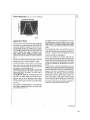
Photolithography was used to fabricate these Dielectrophoreris Traps in the CSU
Cleanroom. This process allows building contacts, wires, and effectively traps on a micron
scale. The DEP chips were built with two distinct components, a DEP trapping circuit and a
microfluidic channel. These two components are bonded together to form a DEP trap.
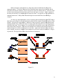
The DEP trapping circuit is composed of three contacts and three discrete lines running
through the area under the channel. The conductive material used was gold and chrome. These
metals were first deposited onto a glass slide using an Evaporator in the cleanroom. A layer
30nm of chrome was first deposited onto the slide. This thin layer of chrome is deposited
because chrome can adhere to glass much better than gold can. A 120nm layer of gold is then
placed over the chrome layer. Gold is deposited because of its low resistance. Once this
deposition is completed, photolithography follows. AZ1512 Photoresist is placed and then spun
on the chip. This resist is thinner and has very good resolution. A soft bake at 110 degrees
Celsius for 1 minute follows. Next the chrome DEP mask is used to pattern the resist. A chrome
mask is chosen for this exposure because of the small features it encompasses. Chrome masks
are expensive but have a high resolution and have an antireflective coating to enhance the
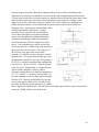
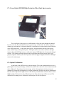
exposure. This mask contains two different trapping
circuits to select from. A characterization of the AZ1512
resist found and exposure time with the soft bake of 10
seconds. The resist is exposed for 10 seconds which
maximizes the resolution of the resist. The exposed resist
is then developed leaving the unexposed area covered. A
two step wet etch removes the uncovered gold and
4