1
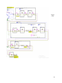
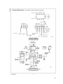
Optical Biosensors
Second Semester Report
Spring Semester 2008
by
Allan Fierro
David Sehrt
Doug Trujillo
Evan Vlcek
Michael Bretz
Prepared to partially fulfill the requirements for
ECE402
Department of Electrical and Computer Engineering
Colorado State University
Fort Collins, Colorado 80523
Report Approved: __________________________________
Project Advisor
__________________________________
Senior Design Coordinator
ABSTRACT
Currently cell sorting is both an expensive and arduous task. Optofluidic Intracavity
Spectroscopy (OFIS) is a low-cost, attractive alternative to these other cell sorting methods such
as flow cytometry. Unlike flow cytometry, OFIS doesn’t contaminate the samples with
fluorescent tagging. OFIS relies instead on index of refraction of the cells, which allows for
observation of these cells in their natural state. The current procedure for OFIS demands an
observer to monitor cells flowing through a microfluidic channel, trap a cell, and set up a
spectrometer reading. This demands valuable time of the observer and makes cell differentiation
unnecessarily slow. In order to improve the speed of OFIS, an automation system must be
implemented to detect cells, trap them, and take a measurement. To achieve acceptable speed
through OFIS new hardware was engineered which includes new fabrication techniques for
making the polydimethylsiloxane PDMS/glass chips with micro-fluidic channels with
dielectrophoretic (DEP) traps, flow control, a detection circuit with a high gain transimpedance
amplifier, a RF switch and Labview software to control the system. Each of these components
required innovative thinking to improve cell differentiation with OFIS.
1
TABLE OF CONTENTS
I: Introduction …………………………………………………………………………………
3
II: Channel Fabrication ……………………………………………………………………......
5
III: DEP Chip Micro-Fluidic Ports …………………………………………………………....
IV: Flow Control …………………………………..………………………………………......
V: Detection Circuit ……………..…………………………………………………………….
VI: RF Switching. ……………..………………………………………………........................
VII: DEP Trapping ..…………..………………………………………………........................
VIII: Future Work ……………..……………………………………………………………….
References ……………………………………………………………………………………..
Appendix A – Abbreviations ……………..………………………………………….………...
Appendix B – Budget ……………..……………………………………………………………
Appendix C – Peripherals ……………………………………………………………………...
Appendix D – Project Tips and Tricks ………………………………………………………...
Appendix E – Data Sheets and User Manuals …………………………………………………
Acknowlegements ………………………………...……………………………………………
8
10
13
18
18
15
22
23
23
24
34
39
57
FIGURES
Figure 2.1 ………………………………………………………………………………………
Figure 2.2 ………………………………………………………………………………………
Figure 3.1 ………………………………………………………………………………………
Figure 3.2 ………………………………………………………………………………………
Figure 4 ………………………………………………………………………………………...
Figure 5.1 ………………………………………………………………………………………
Figure 5.2 ………………………………………………………………………………………
Figure 5.3 ………………………………………………………………………………………
Figure 5.4 ………………………………………………………………………………………
Figure 5.5 ………………………………………………………………………………………
Figure 5.6 ………………………………………………………………………………………
Figure 5.7 ………………………………………………………………………………………
Figure 5.8 ………………………………………………………………………………………
Figure 6.1 ………………………………………………………………………………………
Figure 6.2 ………………………………………………………………………………………
Figure C1.1 …………………………………………………………………………………….
Figure C1.2 …………………………………………………………………………………….
5
7
8
9
11
13
13
14
15
16
16
16
16
20
21
25
26
2
Figure C1.3 …………………………………………………………………………………….
Figure C2.1 …………………………………………………………………………………….
Figure C2.2 …………………………………………………………………………………….
Figure C2.3 …………………………………………………………………………………….
Figure C2.4 …………………………………………………………………………………….
Figure C2.5 …………………………………………………………………………………….
Figure E2.1 …………………………………………………………………………………….
Figure E2.2 …………………………………………………………………………………….
27
30
31
31
32
33
36
38
Chapter I: Introduction
As of right now, the main procedure for distinguishing cells apart is flow cytometry. We
are working on a more cost efficient method called optofluidic intracavity spectroscopy (OFIS).
This procedure has the advantage of not using fluorescent tags, which are quite expensive and
add to the time needed for the sample preparation. By using the refraction of light through the
cells instead of fluorescents we can observe the cells in a more natural, or pure, form and
therefore do not have to worry about the chance that the tags may interfere with normal cell
function.
The components of our system are: a microscope, an infrared LED, a cell detection
circuit, a data acquisition unit with analog to digital convertor and digital output, computer
control software, a function generator, a RF switch, a DEP chip with the micro-fluidic channel in
it, and a spectrometer. (See figures below) To date, we have made a channel to flow our sample
solution through. This channel has metal leads (DEP traps) for setting up the electric field to trap
our cell when it is detected by the detection circuit to be analyzed by the spectrometer. We first
had to build the channels with the traps on them. The next step was to determine the proper flow
rate of the solution so as to optimize trapping. We also made a circuit to detect the presence of a
cell to trigger the trap. All of the control was done with Labview software.
The way our system works is as follows. First, light from an inferred light emitting diode
(IR LED) wavelength peak centered at 850nm is focused through the cavity of the micro-fluidic
channel on the chip. The light passes through up to the microscope and out from the microscope
via a fiber optical cable into our detection circuit. This light gets converted into a current in the
nA range using a photodiode and then goes into a transimpedance amplifier to get converted to a
voltage and to be amplified. This voltage is sent to a data acquisition device (DAQ) to compare
the voltage with a preset reference voltage. If the input voltage is below the preset value the
DAQ will send a signal to close the RF switch in order to send a 6 or 10 MHz 10 Vpp signal to
the DEP traps on the chip. This will stop and hold a cell in the trap for analyses by the
spectrometer to distinguish the cell. In order for the DEP trap to be able to capture a cell the
3
sample solution must be flowing at a slow enough rate so as to not have the cells have too much
inertia. This is done by using a micro-pump and software (Labview) to create a pulse width
modulation to have the proper duty cycle to get the flow rate we need.
4
Chapter 2 will discuss the fabrication of our chips and how the channels are made and
how the traps and leads are added to the chip. Chapter 3 will be on DEP chip micro-fluidic
ports. Chapter 4 will discuss the flow control of the microfludics we used plus the pump system.
Chapter 5 will discuss the detection circuit we designed and some of the components used.
Chapter 6 will discuss DEP trapping. Chapter 7 will cover the future work and recommendations
for next year.
Chapter II: Channel Fabrication
Photolithography was used to fabricate these cielectrophoreris traps in the CSU
Cleanroom. This process allows building contacts, wires, and effectively traps on a micron
scale. The DEP chips were built with two distinct components, a DEP trapping circuit and a
microfluidic channel. These two components are bonded together to form a DEP trap.
The DEP trapping circuit is composed of three contacts and three discrete lines running
through the area under the channel. The conductive material used was gold and chrome. These
5
metals were first deposited onto a glass slide using an evaporator in the cleanroom. A layer
30nm thick of chrome was first deposited onto the slide. This thin layer of chrome is deposited
because chrome can adhere to glass much better than gold can. A 120nm layer of gold is then
placed over the chrome layer. Gold is deposited because of its low resistance and low chemical
reactivity. Once this deposition is completed, photolithography follows. AZ1512 Photoresist is
placed and then spun on the chip. This resist is thinner and has very good resolution. A soft
bake at 110 degrees Celsius for 1 minute follows. Next the chrome DEP mask is used to pattern
the resist. A chrome mask is chosen for this exposure because of the small features it
encompasses. Chrome masks are expensive, about $400 for a 3 µm resolution 4”x4” plate, but
have a high resolution and have an antireflective coating to enhance the exposure. This mask
contains patterns for two different trapping circuits to select from. A characterization of the
AZ1512 resist found and exposure time with the soft bake of 10 seconds. The resist is exposed
for 10 seconds which maximizes the resolution of the resist. The exposed resist is then
developed leaving the unexposed area covered. A two step wet etch removes the uncovered gold
and chrome from the glass slide. The DEP trap chip is then ready for two of the three types of
bonding. The DEP channels were composed of either polydimethylsiloxane (PDMS) or glass.
PDMS channels were the majority of the channels prepared since the fabrication success rate of
these channels was much higher than glass. The success of PDMS is attributed to its exceptional
adherence to glass. The PDMS used was made of bulk PDMS and the PDMS curing agent with
a mass ratio of 10:1 respectively. This PDMS is then placed in a vacuum and degassed.
Degassing will remove the impurities in the PDMS which will improve the optical properties of
the molded part. A mold of the channel was needed to form the channel. This mold is composed
of a silicon substrate and SU-8 resist. This epoxy based resist is much thicker and viscous than
the AZ1512 and can be used as a mold when it is baked and fully developed. Once the mold is
constructed PDMS solution is poured into the mold again degassed. Once degassed the mold is
placed in an oven to bake for at least 4 hours. The curing agent transforms this viscous liquid
into an elastic solid. The PDMS can then be cut and peeled off the silicon substrate. A glass
cover slip is then placed on the opposite side of the channel which keeps the PDMS chip clean
and allows the channel to be transported easier. In order for the PDMS channel to be bonded to
the DEP trapping circuit one more step in the DEP circuit must be performed. A gold and
chrome sheet still remains outside of the trapping circuit which is used for other bonding
processes. This area is removed with the same lithography steps as creating the traps except that
a mask covering the trapping circuit is used. Now the two chips are ready to be bonded together.
The DEP chip is taped to a glass slide with the circuit
facing out. Both chips are then oxygen-plasma treated
with a micro-RIE. After treatment the two chips are
bonded together using the mask aligner. The PDMS
channel is placed on the stage facing up. The DEP chip is
positioned facing down being held in the mask holder.
The DEP traps are then positioned over the channel. The
6
channel is then brought into contact with the DEP circuit chip. The two are now bonded
together. The mask holder is then unscrewed and pulled out vertically from the aligner.
Glass channels were experimented with as well. These glass channels are more desirable
than PDMS because a dielectric coating can be deposited on the surface of glass producing a
optical cavity necessary for cell differentiation. Pyrex glass is used for channel etching and
chrome and gold are deposited on the surface. A thick layer of P4400 positive resist is deposited
onto the surface. This resist was chosen because it is much thicker than the AZ1512 resist which
will be necessary with HF etching. The tradeoff with using P4400 is that it doesn’t have as good
a resolution as AZ1512. In this application giving up resolution is certainly acceptable. The soft
bake for this resist is 110 degrees Celsius for 2 minutes. The resist is then exposed with the
channel mask for 35 seconds. The exposed area is washed away in development. The chip is
then baked at 110 degrees Celsius for 10 minutes. This turns the resist into a hard film which
can withstand the wet etching process. The gold and chrome are etched away. The next step is
to etch the glass. This is done using a wet etch of HF. The chip is placed in HF for
approximately 3-4 minutes. The chip is
removed from the HF and washed with
de-ionized water. The chip is then
placed in an acetone bath to remove the
hardened resist. Acceptable glass
etching was never achieved in the
semester. The channel surface must be
as uniform as possible to provide better
transmission of light. Using an Alpha
Step surface profilometer to measure the
surface height, deep indents were found
in the glass. One explanation to this result is that there are lattice impurities in the glass that etch
faster than the uniform lattice. If this were the case then higher quality glass would be needed to
perform suitable glass etching.
Once the layer of resist is removed, the channel chip can be bonded to the DEP trapping
circuit chip. Two bonding methods have been implemented. The more successful method is
Indium bonding. A piece of Indium metal and the channel with gold on the outer area are placed
in a solution. A positive voltage is applied to the Indium metal and a negative voltage is place on
the of the channel chip. This creates a current of Indium to be deposited on the gold. The
channel chip is then ready to bond to the DEP circuit chip. The two pieces are roughly aligned
by eye and pressed together by hand. The chips are then observed under a microscope to view
the alignment. Fine adjustments are made to optimize the alignment. Once the alignment is
made the two chips are sandwiched between two copper sheets. These sheets are then put in a
vise. The vise is screwed together with four screws. This puts equal pressure on the bonding
area. The bonding vise is then placed into a heater. A vacuum is pulled in the heater to prevent
7
oxidation from the high temperatures. The temperature in the heater is controlled by a
programmable unit attached to the heater. The temperature is then programmed to ramp up to
and hold at a certain temperature and then ramp down. Once the desire temperature program
completes, the bonding vice is pulled from the heater. The channel and the DEP trapping circuit
chips are now bonded together.
A similar bonding procedure is gold to gold bonding. The advantage gold has over
Indium is that the height of the material required for bonding is minimal compared to Indium.
Minimizing the height for bonding is critical because the height dictates how leaky the channel
will become. Indium bonding adds another layer in the bonding area outside of the chip. This
layer adds an additional height on the scale of microns. This will produce a leakier channel than
chips bonded with a gold to gold method. This gold to gold method has not successfully been
completed on test chips. These test chips are half the size of the DEP trapping circuit chips and
have gold with no patterning. The two gold chips are pressed together and put between the
copper plates and into the vice. The temperature is programmed to be much higher than indium
bonding. This is due to the fact that Indium bonds much easier to surfaces than gold does to gold
or any other surface. The melting point of gold is also very high. In order to fuse the two pieces
together a very high temperature must be obtained. An appropriate temperature and pressure
have no been obtained which prevent acceptable bonding. Small bonding areas have been
obtained but not large enough to be a reliable method for chip bonding.
Given the difficulty of metal bonding, alternative approaches were explored but have not
yet been incorporated in actual micro-fluidic channels.
Chapter III: DEP Chip Micro-Fluidic Ports
In order to get cells into the DEP chip with a micro-channel, there must
cells to physically enter the chip. It is also important that there is a way for the
the chip. This is accomplished through the use of nanoports. There are two
nanoports on every chip, one for the cells to enter into the channel, and one for
cells to exit the channel. Nanoports are cylindrical shaped parts that are on the
– 2 cm in diameter and 2 – 3 cm tall. They are composed of a plastic-like
material. On the bottom of the nanoports, there is a
small circular opening with a rubber seal surrounding it. From the top,
nanoports are hollow with threads so that a nanotube can be secured into the
nanoport using a hollow screw-like adapter. These adapters are included as
when nanoports are purchased. Nanotubes are very small
tubing that are 150 µm in inner diameter that are frequently used in microfluidics. The figure shows the basic structure of a nanoport.
be a way for
cells to exit
order of 1
a kit
8
Figure 3.1: Nanotube-Nanoport Interface
Before nanoports can be placed on a chip, holes must be drilled into the chip in the
appropriate places. To do this, a pattern of the chip fabrication is placed over the chip and the
two places for holes are marked. Then a drill press is used with a small drill bit. Great care must
be taken when drilling the holes because glass cracks and chips very easily. Water is applied at
the drill area and only very small depths are drilled at a time. This process is very dependent on
minimal human error. Many of the fabricated chips have non-ideal holes when drilling is
complete.
It is also very important to have a way to securely place the nanoports on the DEP chip so
that there is no leakage as cells and liquids are pushed into the channel and pulled back out of the
channel, sometimes under high pressure. The nanoport attachment process is quite simple and
never fails no matter how dirty the sample is, even for the non-adhesive type described below.
Adhesive o rings are used to create the bond between the nanoport and the chip. Adhesive o
rings are a sticky, glue-like material in an “O” shape that act as double-sided tape. These rings
are very carefully placed around the center of the drilled holes, and pressed firmly into place.
After this, the nanoports are cautiously placed on the adhesive o rings, making sure to center the
nanoport over the hole. Again, this is pressed firmly into place. Once complete, the chip is
clamped to the nanoport for one hour to allow the adhesive o ring to dry and seal. The figure
below shows the placement of a nanoport.
9
Figure 3.2: Nanoport Attachment
Second Semester Updates
The company that made the adhesive o rings no longer produces them. Their
replacement o rings are non-sticky and bond via heat. The process for attaching a nanoport is
nearly identical; however the final step is to bake the chip in 170˚C for 1 hour. Placing the o ring
and nanoport is much more difficult because the new o ring is not sticky. The bonding strength
of the new o ring is very dependent on the cleanliness of the surfaces that are being bonded. A
detailed description of the process of attaching the new nanoports is in Appendix E.
Chapter IV: Flow Control
An essential part of the project is to be able to get cells into the chip. There are several
considerations for acceptable means to accomplish the desired flow rate of cells in the channel of
the chip. The first and primary requirement is that the flow rate must be less than or equal to
40 µm per second (40 µm/s). This requirement comes from the DEP traps on the chip. If the
flow rate exceeds 40 µm/s the force of the DEP trap to stop a cell will not be sufficient to stop a
cell and hold it in place. Another limitation of flow control is that there must not be too much
10
pressure on the nanoport-chip seal or in the channel. The bonding on glass to glass chips is not
very strong and high micro-fluidic pressure will cause the chip to leak. If leaking is severe, it is
possible for cells to flow outside of the channel. Obviously, this is very undesirable because all
of the traps and optical detection are near the center of the channel. It is also worth noting that
all of the glass chips have gaps between the two pieces of glass due to an imperfect bonding
process. This creates flow outside of the channel and different fluid dynamics than the PDMS
chips. Because the glass to glass chips (glass chips) essentially have larger channels, the flow
rate is significantly slower than in the PDMS chips when the same amount of pressure is applied
to the fluid.
Most cell samples, such as blood, are obtained using a syringe. Therefore, a syringe is
used to push samples into a nanotube and into the channel. Although the end goal of the project
is to pump cells through the channel and analyze them, it is impractical to actually use cell
samples to develop and test flow control. Therefore, de-ionized water was used with glass
spheres ranging from 5 µm to 26 µm in diameter. The majority of the time 9.77 µm spheres
were used. This water with glass spheres will be referred to as “fluid” in parts of this section.
When the project first began, it was thought that the rate at which the end of a syringe plunger
needed to be pushed could be calculated based on the fact that the volume in is the same as the
volume out. Ideally, chips are fabricated with a 200 µm wide by 25 µm deep channel. This
gives an ideal cross-sectional area of 200 µm × 25 µm = 5000 µm2. If the syringe plunger is
pushed at a rate of x µm/s then the volume of fluid flowing into the nanotube (and the chip) is
π × (0.5 × diameter of syringe [µm])2 × x µm/s = z µm3/s. This flow rate must logically be the
same in the channel since the volume in must equal the volume out. This result can then be used
to calculate the velocity at which fluid will travel through the channel. The equation is as
follows: v µm/s = z µm3/s × (5000 µm2)-1. Substituting the first equation into the second gives a
direct relationship between the velocity of fluid in the channel v [µm/s] and the velocity at which
the plunger of the syringe is pushed x [µm/s]. This resulting equation is:
v µm/s = x µm/s × π × (0.5 × diameter of syringe [µm])2 × (5000 µm2)-1
The only syringes on hand at the beginning of the project were 3 cc syringes with a
diameter of 8.585 mm = 8585 µm manufactured by B-D. Using the equation above equation, to
achieve a 40 µm/s flow rate in the channel, the plunger must be pushed at a rate of 0.00346
µm/s. The original plan for flow control was an industrial syringe pump. Borrowed from the
chemistry department, the NE – 1000 syringe pump made by New Era Pump Systems, Inc. can
push this B-D syringe at a rate of 2.434 µL/hr. This is the equivalent of
6.761 × 105 µm/s. This is 1.954 × 10⁸ times too fast! Obviously this syringe pump is not a valid
solution to the flow rate problem. In addition, when the syringe pump was set to its slowest
setting, the torque broke the encoder coupler because the pressure in the chip created a force
pushing back against the syringe plunger that was beyond what the pump was designed for.
As a solution, the Oriel Instruments Encoder Mike Controller 18011 was chosen to
function as a custom pump. The Oriel Instruments Encoder Mike Controller 18011 (Oriel) is
designed to be used as a precise way to move a microscope stage. It can move the actuator at a
minimum velocity of 0.5 µm, which is still about 150 times faster than the desired rate for the
larger syringe (8.585 mm diameter). To reduce the rate at which the plunger must move, a
11
smaller syringe (4.669 mm diameter) was chosen to be used in the system. This syringe plunger
only needs to move at a rate of 0.0115 µm/s to achieve the desired flow rate of 40 µm/s in the
channel. Because this is still slower than what the Oriel is capable of, Labview software was
used to create a duty cycle where the actuator is only moving for a small percentage of the time.
For details on how the Oriel was implemented into the system, see Appendix C2. To achieve
40 µm/s velocity inside the channel, the Labview VI was set so that the actuator moved for 0.825
seconds at 0.5 µm/s (0.4125 µm) and off for 7 seconds. When the VI is used, the optimal flow
rate occurs at this duty cycle of approximately 10.5%. This “duty cycle” description applies to
the movement of the actuator. However, “duty cycle” is not an accurate comparison because the
flow rate in the channel takes much longer to decay than the 7 second period during which the
pump is turned off. This is discussed more later Another consideration is that the stage mounted
to the actuator is spring-loaded and adds complication to the analysis. This spring action actually
allows the plunger to be pushed at a rate slower than the 0.5 µm/s that the actuator is moving.
Figure 4
Through experimentation, it was quickly discovered that the derived equation does not
hold true for glass chips, but is reasonable for PDMS chips. This is because the actual crosssection in a glass chip’s channel is larger and cannot be accurately estimated. Experimentation
also revealed that due to complex pressure dynamics, the flow rate in the channel does not follow
the syringe plunger. To be more precise, when the plunger is moved and then stopped, the flow
in the channel does not stop immediately, but rather decays over the course of several minutes.
This behavior is analogous to the behavior of an RC circuit. Both have a time constant
associated with how long it takes the flow rate to die down. The larger syringe (8.585 mm
12
diameter) builds up a higher pressure and the time constant is several times longer than the time
constant for the smaller syringe (4.699 mm diameter). This suggests that the cross-sectional area
of the syringe is proportional to the time constant for the flow rate inside the channelAll of these
more complex dynamics make experimentation the best indication of actual flow inside the
channel. There was no precise way to obtain the velocity of spheres moving in the channel but
the duty cycle described earlier is estimated to produce a flow rate of 40 µm/s in a PDMS
channel. Due to limited fabrication of glass chips near the end of the semester, the duty cycle for
the desired flow rate in a glass chip has not been found. However, it is known that the duty cycle
must be higher than that for the PDMS channel.
Second Semester Updates
Spheres often get trapped on the edges of the drilled hole when pumping a solution
through the channel. To deal with this problem, a new set of solutions were made and
documented. These solutions are more dilute and should allow for operation with less clogging.
The new 9.77 µm sphere solution is 0.05 cc of sphere solution to 7 cc of de-ionized water. The
new 7 µm sphere solution is 4 cc of sphere solution to 10 cc of de-ionized water
Perhaps the most prominent problem that hindered the project is leaking chips. Chips
often leak at the nanoport-glass barrier. Another common place that chips leak is the edges of
the chips where the glass-to-glass bonding or PDMS-to-glass bonding occurs. Glass-to-glass
bonding problems cause leaking and this problem is more extensively discussed in Chapter II:
Channel Fabrication. Many leaks cause fluid to flow outside the channel or not in the channel at
all. The most effective method of fixing leaking chips is UV glue. However, UV glue can only
be used to patch the outside of a chip, not where glass-to-glass or PDMS-to-glass bonding has
failed. Therefore, patching the perimeter of a chip or the nanoports can prevent leaking, but not
flow outside the channel within the chip. The UV glue is mostly transparent and does not harden
until exposed to ultraviolet light. After applying UV glue to the necessary part(s) of the chip, the
glue must cure in the ultraviolet light for at least 5 minutes. Experimentation has found that 15
minutes of curing seems to be more appropriate.
13
Chapter V: Detection Circuit
We needed to be able to tell when a cell was present in our system. For this we decided
to design a detection circuit. This circuit would detect a cell by a modification in the light
intensity. In order to design the detection circuit we started with a ST connectorized
photodetector (OPF482) connected to a 62.5 um core diameter multimode fiber optic cable. The
light from an infrared LED goes into the microscope and then through the fiber optical cable into
the photodetector A photodetector is a photodiode which is a component with a p-n junction.
When a photon, light, of sufficient energy strikes
the diode, it excites an electron in the valence
band thereby creating a mobile electron and a
positively charged electron hole. If the absorption
occurs in the junction's depletion region, or on
average one diffusion length away from it, these
carriers are swept from the junction by the built-in
field of the depletion region, producing a
photocurrent. Photodiodes can be used in either
the zero bias mode, known as the photovoltaic
mode, or in the reverse bias mode, known as the
photoconductive mode, the mode we are
interested in. In the zero bias mode, light striking
the diode causes a current across the device which
leads to a forward bias of the diode which in turn
induces “dark current” in the opposite direction to
the photocurrent. Dark current is the relatively
small electric current that flows through a
photodiode even when no photons are entering the
device. This is called the photovoltaic effect and
is the basis for how solar cells work, which are
just a large number of big photodiodes. Onto
reverse bias which only induces a little current
(known as saturation or back current) along its
direction But a more important effect of reverse
bias is widening of the depletion layer (therefore expanding the collection volume) and
strengthening the photocurrent. Circuits based on this effect are more sensitive to light than ones
based on the photovoltaic effect and also tend to have lower capacitance due to the greater
separation of the charges, which improves the speed of their time response, because τ=RC so the
smaller the capacitance the smaller the time constant. On the other hand, the photovoltaic mode
tends to exhibit less electronic noise. Another type of photodiodes is the avalanche photodiodes
which have a similar structure, but are operated with a much higher reverse bias which allows
each photo generated carrier to be multiplied by avalanche breakdown resulting in internal gain
within the photodiode, which increases the effective responsively of the device. Our
photodetector is used in reverse bias with a large resistor (1.8MΩ) to have the majority of the
14
current flow into the circuit. The next step of the circuit is a low-pass filter with a cutoff
frequency of 1,000 Hz to reduce the noise from the photodetector. The output from the filter
goes into the operational amplifier or op-amp. The op-amp, a LF412CN, is setup in a noninverting configuration with a gain (1 + R2/R1) of 2,500. After the op-amp stage, we have a
voltage buffer or voltage follower, used as a buffer amplifier, which is used to eliminate loading
effects or to interface impedances. Vout = Vin with Zin = ∞ in theory, but in reality it is the input
impedance of the op-amp, which is usually 1MΩ to 1TΩ. Some of the difficulties we ran into
were a noisy signal, which is why we added a low pass filter, having the op-amp oscillate so we
added some capacitors to eliminate this. We also had a weak input signal which is why we
increase the resistor to 1.8MΩ. Below is the final circuit
+5 VDC
C5
0
+5 VDC
100n
+5 VDC
2
C7
D1
PHOTODIODE
C9
0
0
100n
100n
U1A
8
8
3 +
1
5 +
2 -
R1
250k
C1
9n
C6
LF412
0
A1
LF412
0
-5 VDC
0
7
C10
100n
0
U1B
6 4
3.2k
4
1
R2
100n
-5 VDC
R5
124k
C8
1n
R4
100
0
Figure 5.3
15
Second Semester Updates
Due to many problems with the previous circuit design such as noise causing errors in
our results and simply not enough gain, we redesigned the entire light modulation detection
circuit.
The redesigned circuit (Figure 5.4) is still based around the premise of the previous
circuit’s transimpedance stage, but uses a different configuration. It was seemingly problematic
to use a resistor based transimpedance such as R1 in Figure 5.3 to generate a voltage based off of
the photocurrents, as the photocurrents ranged from 900 nA to 5 µA and the amount of external
electromagnetic interference seemed to be enough to cause erroneous values. The redesigned
circuit takes advantage of a transimpedance amplifier (TIA) configuration shown in figure 5.4 as
well as a voltage amplifier.
Figure 5.4
16
The first stage of the circuit (Figure 5.5) is the TIA with a transimpedance gain of
4.4MΩ. The second stage of the circuit (Figure 5.6) is the voltage amplifier, taking the voltage
output from the TIA and applying a gain of 700 V/V.
Figure 5.5
Figure 5.6
Noise was still seen as a problem with this new circuit. Noise of about 60 Hz was seen on
the output of our amplification stages, which caused unreliable results while automating as it
created a 30-50 mV difference on the output of the circuit. The noise was dealt with by the use of
the low pass filter (LPF – Figure 5.7) as well as decoupling the power supplies from the circuit
(Figure 5.8). The LPF can be seen as the capacitor C1 in parallel with the feedback resistor R1.
This LPF limits the overall bandwidth of the circuit causing a slower time response, but is
required to limit the amount of noise from the input signal. The capacitors on the power supplies
act to decouple the supply lines from the circuit, which greatly limits the destabilizing effects of
the inductive response the supplies cause when applying a load. We also created an aluminum
enclosure to house the circuit in order to stop any electromagnetic interference.
Figure 5.7
Figure 5.8
17
The time response is now the biggest issue with the circuitry. The limited bandwidth due
to the LPF has caused the overall system performance to decrease. The amplification stage
produces the largest time constant of the system, and is the cause of the issues with a slow time
response. In order to achieve a faster time response, we could either tweak the LPF for optimal
values, or use an op-amp made for transimpedance configurations, such as Texas Instrument’s
OPA380. What this amplifier provides over our current op-amp, the LF412, is a much larger gain
bandwidth allowing for a greater input signal bandwidth, and also offers great precision and low
noise which is important when trying to amplify currents as low as 1 nano-Ampere.[5]
A future design idea, which would call for a complete redesign of the circuit, would
include an op-amp like the OPA380 and a voltage buffer. To achieve the best distortion
reduction and performance in a transimpedance circuit, all required gain should be taken care of
with the TIA.[4] The output of the gain stage should be followed by a voltage buffer. The same
noise cancellation ideology and capacitive decoupling should be followed from previous designs;
however the low pass filter should be tweaked to acquire a stable phase margin. Ideas for
improving performance with a transimpedance circuit can be found in the datasheet for the
OPA380 [5].
18
Chapter VI: RF Switching
To fully automate the system, the cell traps would have to be turned on when a cell is in
proximity of a trap. To do so, the Data Acquisition Unit (DAQ) would monitor the voltages from
the cell detection circuit until the given voltage exceeds the threshold, showing the presence of a
cell. The DAQ would then create a digital high output on an analog switch or relay and cause a
signal of radio frequency (RF) to be applied to the traps, thus causing a cell to be trapped in an
electromagnetic field. The components we tried to use to switch the RF signal, such as an analog
switch, no longer performed as an ideal switch due to the high frequencies. At RF, the
capacitance associate with the analog switch caused a percentage, usually 10%, of the signal to
leak when the switch was considered open. To avoid problems with RF signals, we chose to use
a Teledyne 172-5 RF DPDT relay, which is designed to handle RF signals.
Chapter VII: Dielectrophoretic (DEP) Trapping
DEP trapping is necessary in this project for one main reason: If the sphere/cell/particle
is not held in a particular position without moving, a spectral reading of light shined through that
object will be extremely difficult to gather data with the equipment and limited budget that we
have. DEP trapping is a method of using electromagnetic forces to hold an object in place. One
might ask the question: how do you exert a force upon a charge neutral object using an electric
field? The answer to this question is not trivial. DEP trapping occurs when a non-uniform
electric field is passed through a neutral body. Internal to the neutral object, the molecules
within the neutral object polarize, much like the depletion region that occurs when a voltage is
put across a pn junction. The imbalance of localized charges results in a virtual electric dipole
being formed within this neutral object. Therefore, the electric field will “apply” a force to the
surface dipoles in the overall neutrally charged object. Since the objects we are concerned with
are on the order of 10 µm in diameter, it is easier to exert a significant enough force on these
small particles with large surface to volume ratios to “push” them into a suitable area to take a
spectral reading.
19
Figure 6.1 Picture of DEP trap electrodes
In order to achieve a non-uniform electric field, a time-varying voltage must be applied
across the electrodes of the DEP trap. The approximate force applied to an object being trapped
can be defined by the formula
[1]
where F refers to the dipole approximation to the DEP force, ε1 refers to the permittivity of the
medium surrounding the object being trapped, R is the radius of the particle, r is the spatial
coordinate, ω is the angular frequency of the applied voltage, E is the complex applied electric
field, CM is the Claussius-Mossotti factor. The Clossius-Mossotti factor is a frequency
dependent function of the permittivity of the medium outside the particle and the inside of the
particle. In simpler terms, the force to push an object into a trap is proportional to the positional
gradient of the electric field. The implications of such a thing is that the particle will experience
a force until it reaches an extrema in the intensity of the electric field (i.e. the positional
derivative of the electric field is zero, and therefore the force will equal zero.) This translates into
basically a restoring force that keeps the particle trapped at a certain point until the electric field
is removed or until a much larger force physically removes the particle from the trapping area.
In the scope of this project, the non-uniform electric field comes from a 5 Vpp sinusoidal
signal across the two electrodes of the traps.
20
Figure 6.2 (a): Electromagnetic Modeling of DEP traps. Reproduced from [2].
Based upon the field lines shown in Figure 6 .2, the point of highest electric field
intensity is approximately in the center of the trap. This provides an optimal trapping point for
which the spectrometer can take a reading.
Chapter VIII: Future Work
Chip bonding has shown to be a critical step in chip fabrication. Failures in PDMS and
thermocompression bonding have not been reliable methods for bonding the trap and channel
pieces together, and more reliable methods need to be found.
With so much variance in chip fabrication, it would be beneficial to create a feedback
control system for flow control. While the current flow control method can achieve desired flow
rates, the velocity of particles in the channel and the volume of throughput are currently human
estimates. Different chips sometimes require different setting in Labview to achieve the same
result. If an accurate way to measure flow rate were achieved, a feedback control system could
allow for the same flow rate even if there are variances in the effective cross-sectional area of
chips’ channels.
The optical system will need to be fine tuned to allow for adequate light modulation on
chips with dielectric coating. This coating significantly reduces the transmitted light intensity
(transmitted power). If we are able to obtain any donations, a higher output infrared LED could
improve the system. Also, if a high performance photo diode was obtained the performance may
improve. Last, the optical detection circuit could be improved in the area of time response.
Using a high-performance transimpedance amplifier designed for photocurrent amplification
may enhance performance. This amplifier should have a larger gain-bandwidth product to allow
for higher frequency response while maintaining the necessary gain and signal-to-noise ratio.
In the future of the project, the spectrometer will become an essential part of the cell
analysis. Data acquisition will need to be automated using Labview software and resulting data
of the cells will allow for cell differentiation. Because it is the shifting of the wavelength that
21
differentiates cell types, the spectrometer is the heart of the system. Triggering DEP traps based
on light modulation (i.e. intensity) is very difficult and may not be feasible with current project
limitations. An alternative to trapping based on light intensity would be to use the spectrometer
and attempt to detect changes in wavelength and trigger the DEP traps accordingly. It may even
be possible in the future to skip the trapping step entirely and simply take data of the cells’
spectrums as they pass. Such alternatives should be investigated along with other possibilities to
improve the rate at which cells can be analyzed.
Another key element to automation is software. Once the spectrometer is implemented
and spectral data is taken, the data needs to be stored in an efficient filing system and analyzed
for the end user. Without software, each spectrum would have to be analyzed by a person and
compared to other data. The software should have statistical data about the analyzed cells and
should have tolerance parameters that can be set by the user to specify what characteristics
determine different cell types.
22
REFERENCES
"What is Optofluidics?" Optofluidics. 2007. 10 Dec. 2007
http://www.optofluidics.caltech.edu/optofluidics/index.html
Yang, Changhuei, and Demetri Psaltis. "Optofluidics: Optofluidics Can Create Small, Cheap
Biophotonic Devices." Laser World. 1 July 2006. 10 Dec. 2007
http://www.laserfocusworld.com/articles/article_display.html?id=259933
[1] J. Voldman, R. Braff, M. Toner, M. Gray, and M. Schmidt, “Holding Forces of
Single-Particle Dielectrophoretic Traps,” Biophysical Journal, Vol. 80, pp 531-541,
January 2001.
[2] W. Wang,H. Shao, K. Lear, “Lab-on-a-Chip Single Particle
Dielectrophoretic (DEP) Traps” powerpoint presentation given March 2006.
[3] Lear, Kevin L., Hua Shao, Weina Wang, and Susan E. Lana. "Optofluidic Intracavity
Spectroscopy of Canine Lymphoma and Lymphocytes." IEEE Explore4 Dec. 2007.
[4] McGoldrick, Paul, ed. "TI OPA380." Wireless ZONE. 10 May 2004. 20 Mar. 2008
http://www.en-genius.net/site/zones/wirelessZONE/product_reviews/hfp_051004
[5] "OPA 380." Texas Instruments. Sept. 2007. 20 Feb. 2008
<http://focus.ti.com/lit/ds/symlink/opa380.pdf>.
23
APPENDIX OR APPENDICES
- Appendix A: Abbreviations
AC – Alternating Current
DAQ – Data Acquisition Unit
DC – Direct Current
DEP – Dielectrophoretic
LED – Light Emitting Diode
OFIS – Optofluidic Intracavity Spectroscopy
OpAmp – Operational Amplifier
PDMS – Polydimethylsiloxane
VI – Labview Virtual Instrument
Vpp – Volts Peak-to-Peak
- Appendix B: Budget
•
•
•
•
ADG 452 Digital Switch -- $15
Various circuit elements including Op-amps and digital chips -- $10
Hytek iUSBDAQ U120816 -- $105
TOTAL EXPENSES = $130
Starting Budget = $500 over 2 semesters
Money left = $500-$130=$370
24
- Appendix C: Peripherals
The need for peripherals in this project is abundantly apparent. We used many different
measurement and control systems to be able to achieve our goals. These peripherals were:
- Data Acquisition Unit ( iUSBDAQ-U120816) from Hytek Automation
- Ocean Optics Spectrometer (HR2000)
- Oriel Instruments Encoder Mike Controller (18011)
- Microscope (heavily customized Olympus 230997)
- Logitech USB camera
- Beam splitter (Newport parts manufactured in-house)
C1: Data Acquisition Unit
Figure C1.1 Hytek Data Acquisition Unit
The data acquisition unit was brought on board due to a need for triggering a circuit
based on amount of light collected by the photodiode. This made it so that instead of creating a
new logic circuit every time we changed the gain stage of the amplifier, the logic could be
controlled with a Labview VI. This also took out the guess work for a logic chip. In the
specification sheet for a 7400 series logic component, there was a large range of voltages that
were specified to be undefined logic. The DAQ took a lot of the uncertainty out of the logic.
The DAQ is accurate to within 3 mV DC on its 8 available channels of analog inputs. It also can
25
output digital logic at 5 V DC on one of its 18 Digital I/O channels. This may seem like it’s
overkill to have so many, but the DAQ was 2/3 of the price of some of the other data acquisition
units that are on the market. It has a sampling rate of 13,000 samples per second on a single
channel. More expensive units were about the same or even worse. We designed a Labview VI
that would take an analog input, compare it to some specified reference, and output a digital
signal based upon whether or not it was higher or lower than the given reference.
Here is the front panel of the Labview VI:
Figure C1.2 Front Panel of DAQ VI
The interface is quite simple. The triggering voltage is input in the field labeled
“Comparison Voltage”. The channel of the analog input is easily configured. Any errors are
easily read on the error out field. Since we configured the DAQ to take inputs on analog channel
0 (the default value), getting a digital output based upon comparing to a preset voltage was as
easy as inputting the comparison voltage, and hitting the run button in Labview.
The VI for controlling the DAQ was not difficult to program. Another reason we went
with this DAQ was due to the fact that Labview VI’s were available on the Hytek Automation
website. This made it so that it was a “plug and chug” type of program.
26
Here is the VI block diagram:
Figure
C1.3 Block Diagram of DAQ VI
The algorithm used for trapping is described as follows:
Stage 1: The first thing that needed to be done was to be able to read the output of our light
modulation circuit. This was accomplished by using the Hytek Data Acquisition Unit. The
Hytek has analog to digital capabilities, and drivers available on the Hytek website to allow for a
conversion of an analog signal to a 16 bit floating point number. This allows for approximately
three decimal place precision on the readings from the light modulation circuit.
Stage 2: Once the reading is taken from the light modulation circuit and converted to a floating
point number, the second thing that is done in this algorithm is to compare that number to a fixed
value. The fixed value that we have been using is the average voltage reading from the light
modulation circuit when no sphere is present within the trapping area and the reading when
there is a sphere present. This creates a buffer by which particulates and various fluctuations in
the output voltage would not set off the traps. For example, generally the output voltage without
a sphere in the trapping area is approximately 3 V. When a sphere is in the trapping area, the
voltage drops to 2 V. Therefore the comparison voltage would be 2.5 V. That way, if a small
particulate were to flow into the trap area, we would not have a false trapping. Also, if the
voltage of the output were to fluctuate by 10% without a sphere being in the trap, the worst case
scenario would be a 2.7V output vs. 3V. This would still allow operation to work without
creating a false trapping situation.
Stage 3: Once the comparison occurs, it sets the value of a boolean variable. This boolean is true
if the voltage was less than the fixed value and false if greater than the fixed value. If a false is
generated in this boolean variable, then the algorithm goes back to stage 1 to read in a new value.
If a true is generated, then the Hytek's capabilities are exploited again. The Hytek has drivers to
27
send out digital signals of either 0 or 5V. When the boolean variable is true, the Hytek sends a
digital signal to apply an RF signal to the traps, theoretically trapping the cell.
Stage 4 (future work): Once the cell is trapped, the spectrometer will take it's reading, store it in
a file to be read by the user. This has not yet been implemented, but it is planned to be done in
the future. Currently, we are modeling this as a delay of 500 ms.
Stage 5: Once the spectral reading is taken, the digital signal that is applied to send the RF signal
to the traps is set to 0V, and the sphere will be released.
Stage 6: In order for there to be no “re-trapping” of the same cell, there is a small delay of 500
ms after the trap is released to allow time for the recently trapped cell to clear the trapping area
before another voltage reading is taken. From this stage, process starts over again until
terminated by the user.
28
Here is a flow chart of the algorithm:
Read Input from
Circuit
Compare Input
Value to Fixed
Value
Wait for Cell to
Leave Trapping
area
Is Input Value
Less than Fixed
Value?
No
Yes
Release Cell
Trap Cell
29
C2: Oriel Instruments Encoder Mike Controller 18011
(a)
(b)
Figure C.2.1(a) Control Panel of Oriel Controller (b) Microscope stage being controlled
The Oriel Instruments Encoder Mike Controller is normally used as a microscope stage
controller to move a microscope stage very slowly. Our application of this piece of equipment
was as a syringe pump. The main reason that this was used is because it was able to move a
syringe plunger slow enough to get reasonably slow flow within the channel of the chip. The
minimum rate at which the actuator can move is 0.5 µm/s. Remember that the chip only had a
cross-sectional area of approximately 5000 µm2. The syringe that we are using is approximately
0.5 cm in diameter. This makes it so that the stage must be moving extremely slow in order to
get a flow rate within the channel to be as slow 40 µm per second, which is the flow rate by
which it is suitable to trap cells. Again, we used Labview to control the actuator. This was much
more difficult to control because there were no VIs available on the internet. This made for a
much bigger challenge because we were unfamiliar with RS-232 communication that was
required for control of the Oriel actuator. Using a wiring diagram that was in the User’s manual
of the Oriel actuator, we created our own RS-232 to DB9 cable to interface between the control
panel and a computer.
30
Figure C2.2
(a)
(b)
Figure C2.3(a)RS232 input to Oriel Controller
Figure C2.3(b) DB9 input to computer
31
A Labview VI controls the signals that are put on the different wires of the RS-232
Cable. The front panel for the Labview VI looks like this:
Figure C2.4 Front Panel of Oriel Controller VI
The switches in the lower right portion of the front panel control what the switch actually
does. Only one switch can be on at one given time in order to function properly. When the VI is
run with only the pump switch on, the pump will run for a total of 2*(Delay Before Read) + the
time value(ms) specified in the top left input box. When the VI is run with the stop switch
turned on, it will stop all pumping functions. With only the manual command switch turned on,
a string will be sent to the Oriel controller. For example, the string “V200/n” will command the
Oriel actuator to move at a velocity of 200 µm/second. There are many commands like this that
the VI already uses to control the actuator within the VI itself, such as run and stop. The way
that the pump command works is that it will send a run command. Then there will be a specified
delay time, followed by the stop command being sent to the controller, then a second specified
delay. The loop starts over starting with a run command. This allows the user to specify a duty
cycle for the pump. The values that we used for this VI were: time on = 725 ms, delay before
write = 50 ms, delay before read = 50 ms, and time off = 7000 ms. This roughly gave a flow rate
of 40 µm per second. The VI block diagram shows all of the internal logic that occurs with the
switches, and with the delays, as well as the Run and Stop commands sent to the Oriel actuator.
32
Figure
C2.5
33
C3: Ocean Optics HR2000 High-Resolution Fiber Optic Spectrometer
The overall goal of the project is to differentiate cells as they pass through the channel.
In order to do this, the method of intracavity spectroscopy will be used. In order to detect the
changes in wavelength as a cell passes through, a spectrometer is used to analyze the diffraction
of the LED light source. At this point in the project, the spectrometer has only been used to
assist with the setup of the optical system. The spectrometer was used to maximize the light
intensity from the LED light source as well as the focused LED light after it has passed through
the lens. The resulting spectrum also provided verification that the microscope optics were
properly aligned. Narrow peaks in the spectrum indicated proper alignment from the LED light
source to the microscope.
34
- Appendix D: Project Tips and Tricks
D1: Attaching Nanoports
The recommended procedure is below:
1. Clean the chip around the drilled hole and the bottom of the nanoport using acetone,
methanol, and de-ionized water. It must be cleaned in this order using 3 different
Q-tips to scrub the surface. The next “cleaner” must be applied before the previous
one dries. Putting the specimen to be cleaned in a glass dish is usually easier in that
there can be an excess of the cleaner, making it take longer to dry. It must be glass
because plastic reacts with acetone. Use an air gun to blow the surface dry before the
de-ionized water dries. Remember to wear gloves when working with acetone and
methanol.
2. Flip both the chip and the nanoport upside down so that the surface of the chip that
will be bonded is facing downward and the surface of the nanoport that will be
bonded is facing upward.
3. Center the o ring on the nanoport surface and bring the nanoport into contact with the
chip, centering the nanoport over the drilled hole on the chip. Notice that the o ring
should be between the chip and nanoport.
4. While holding the nanoport in place, use a pair of tweezers to grab the sides of the
nanoport and press it against the chip while applying pressure on the center of the
opposite side of the chip with a finger. This should allow the placement of a clamp
over the nanoport and chip, holding the 2 together, without fingers in the way.
5. Place a clamp over the nanoport and chip holding the 2 together. Make sure that the
clamp is centered and applying even pressure across the nanoport surface before
releasing the tweezers hold on the nanoport.
6. Put the chip with the nanoport clamped on in the oven and bake it at 170˚C for 1
hour.
7. Remove the chip from the oven and allow to cool.
35
D2: Optical Calibration
At the heart of the OFIS process is the microscope. This is the instrument that we use to
gather light to use for spectroscopy, cell detection, and for the camera. No other instrument needs
to be calibrated as frequently as the microscope, and no other instrument in the process can
dramatically change the resulting data by a slight adjustment. Therefore the correct calibration of
both the microscope and the light source is vital for any reasonable data collection from a microfluidic sample. In this section, the calibration process of the microscope will be covered. The
difficulties in learning how to calibrate the microscope will also be explored.
To begin, the basic knowledge of how our system works is essential. Below, is a figure
on the general set up of the entire system. The size of the optic fiber coupled into the beam
splitter should be around 50/125 to 62.5/125, and needs to be a multimode fiber. The percentage
of light sent through the optic fiber is 90%, while the remaining 10% of light goes to a camera.
In the system, an infrared LED is used as a light source. Using a lens, this light is focused to a
small spot on the microscope stage where chips are placed to provide high light intensity. The
light that goes into the microscope is then split as described above. Optical fibers then transport
the light to the spectrometer and cell detection circuit (not pictured).
Figure D2.1: Diagram of microscope being coupled with light source
36
Calibrating the optical system is a fairly involved process with many steps and can take
several hours. To calibrate the optical system, follow the steps below:
1. This first step is not truly necessary, but serves as a good reference and is a good way
to start. To get a starting point for calibrating the system, the use of a LED that emits
light in the visible spectrum is useful. Setup the visible-light LED below the
microscope stage and drive the LED to emit light. Place a white piece of paper on
the focusing plane (the microscope stage, where chips will be placed) and use the
focusing lens for the LED to focus the visible light on the same plane (the piece of
paper). The goal of the lens above the LED is to make the light emitted from the LED
confined to a very small area in a circular shape. Note that the lens should be fairly
level if the LED, lens, and focal point are aligned vertically. Once complete, remove
the piece of paper.
2. Turn the microscope light on. Center the infrared LED below the lens where the
microscope light falls (after passing through the hole in the stage and the lens) and
connect it to a current source for operation. Now turn off the microscope light.
3. Carefully rotate the lens out of the path between the LED and microscope (without
changing its height or tilt).
4. Turn on the spectrometer and set it up to take intensity counts. Note that you must
ensure that the optical fiber is connected between the microscope and spectrometer.
Set the reference level for the spectrometer with no light source.
5.
5. Turn on the infrared LED with a 50 mA current. Adjust x and y tilt of the LED to
maximize the intensity counts that the spectrometer reads.
6. Now reposition the lens over the LED (and under the stage). Fine tune (adjust) the
position, tilt, and even height of the lens to maximize the intensity counts on the
spectrometer. We achieved counts of around 3000. Note that although the height
should not have to be repositioned after step 1, fine adjustments often improve the
intensity.
7. Turn off the spectrometer and place a chip on the microscope stage. Use the camera
to focus the microscope on the center of the chip’s channel using the infrared LED as
the light source.
8. Once focused, turn the infrared LED off. Connect an alignment laser (preferably in
the infrared region) to transmit into the viewing plane through an optic fiber. This is
37
basically shinning light in the opposite direction back onto the chip (like from the
spectrometer back to the beam splitter and then the microscope).
9. Light from the laser is seen in the viewing plane via the camera. Adjust the beam
splitter until the laser light is confined to a small, circular area. Our best calibration
had a focal point that was on the order of 10 µm to 15 µm in diameter. This ensures
that the output from the beam splitter is collecting light from an area where the LED
light is focused on and that a cell in this focal point will produce significant light
modulation. It is important while doing this that the laser is at a low power output so
that the camera is not saturated. With our infrared laser we used 0.2 to 0.3 mA of
current to drive output.
Figure E2.2: Example of alignment using a laser
10. Mark the spot on the computer monitor with a marker. Do not move the camera
window on the computer after this mark is made. Turn off the laser and connect the
optical fibers for normal operation with the detection circuit.
11. Turn on the power supplies for the detection circuit. With the chip still in place, turn
on the infrared LED source. Using the marked spot on the computer monitor, verify
that in the open channel there are a few volts output from the detection circuit. Also,
by positioning the marked spot over DEP trap leads and/or other objects in the
channel, verify that the minimum voltage outputs are obtained when the spot is
directly over these objects. Optical calibration is now complete.
The difficulties encountered in the calibration of the microscope were numerous, and
were mainly due to the poor maintenance of the entire instrument. The second difficulty is the
basic concept of the optics.
38
The microscope used for our experiments has been poorly maintained. Dirt and scratches
on the lens are present, which may alter the light collection, but to a lesser degree. The beam
splitter stage was unstable and poorly fitted onto the microscope, and due to budget constraints
has to be fastened to the microscope with zip ties. If our budget constraints allow, we can
machine better housing for the beam splitter. The focusing plane where the micro-fluidic
channels sit is also difficult to use with the channels. Scotch tape is required to steady the chip in
place and leveled with the focusing plane. The use of tape leads to oils from the fingers being
deposited onto the chip, which alters the light characteristics of the chip. Again, if our budget
would allow, we could machine a better focusing plane that would allow us to secure the chip
into place and avoid taping it. The fiber optic output from the beam splitter is also difficult to use
at time, as there is no relief at the ST junction for the fiber optic cable. A relief at the ST junction
would allow for the focal length from the optic fiber to the beam splitter to be changed without
causing stress to the fiber optic cable or having to dissemble the output of the beam splitter.
The knowledge of optics was one of the easier difficulties to overcome with the help of
Dr. Lear. Understanding why we needed a 62.5/125 optic fiber as opposed to a much larger optic
fiber is an example of the problems he helped us overcome. The reason why a 62.5/125 cable is
used to minimize the area in which the light from the beams splitter is collected.
39
- Appendix E: Data Sheets and User Manuals
E1: OPF 482 Optic Fiber Photodiode
40
41
E2: DAQ Comparison
A/D Characteristics
Number of
Channels:
DI-148U
8
DI-158
NI USB6008
LabJack
U3
Measurement
range:
Resolution:
Sampling Rate
10-bit
14400 [Hz]
4
±10V
Variable Depends on
internal gain
setting
12-bit
14400 [Hz]
8
±20V
12-bit
10 [kS/s]
16
±2.4(?)
12-bit
2.5-50 [kS/s]
Digital I/O
Channels
Mininum Required Digital I/O?
DI-148U
6 bi-directional ports
Yes
DI-158
NI USB6008
LabJack
U3
4 bi-directional ports
Yes
12
Yes
20 (Programmable Ports)
Yes
DI-148U
DI-158
NI USB6008
LabJack
U3
Labview
Labview 5
Labview 5
Cost
$50
$99
Site
http://www.dataq.com/products/startkit/di148.htm
http://www.dataq.com/products/startkit/di158.htm
Yes
$159
http://sine.ni.com/nips/cds/view/p/lang/en/nid/14604
Yes
$99
http://www.labjack.com/labjack_u3.php?prodId=25
42
E3: LF412 Operational Amplifier
43
44
45
46
47
48
49
50
51
52
53
E4: Relevant Syringe Pump User Manual Page
54
E5: Infrared LED
55
56
57
ACKNOWLEDGMENTS
We would like to thank Dr. Kevin Lear PhD for his help and guidance, as well as four of his
graduate students, Bob Pownall, Hua (Linda) Shao, Sean Pieper and Weina Wang, for all of their
help.
58