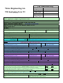
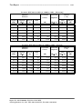
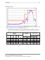
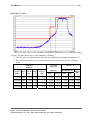
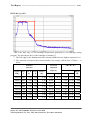
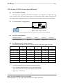
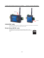
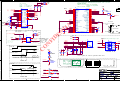
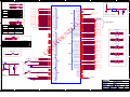
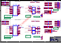
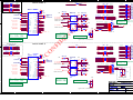
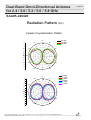
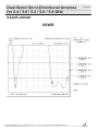
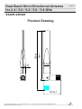
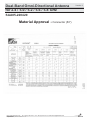
1
TCB TCB GRANT OF EQUIPMENT AUTHORIZATION Certification Issued Under the Authority of the Federal Communications Commission By: Timco Engineering, Inc. 849 NW State Road 45 P.O. Box 370, Newberry, FL 32669 Date of Grant: 05/16/2007 Application Dated: 05/15/2007 Moxa Technologies Co.,Ltd. 4F, No.135, Lane 235, Pao-Chiao Rd. Shing Tien City, Taiwan Attention: Jackie Shi , Manager NOT TRANSFERABLE EQUIPMENT AUTHORIZATION is hereby issued to the named GRANTEE, and is VALID ONLY for the equipment identified hereon for use under the Commission's Rules and Regulations listed below. FCC IDENTIFIER: Name of Grantee: Grant Notes CC SLEW341 Moxa Technologies Co.,Ltd. Equipment Class: Digital Transmission System Notes: RISC-BASED READY-TO-RUN WIRELESS EMBEDDED COMPUTER Output Frequency Watts Range (MHZ) FCC Rule Parts 15C 2412.0 - 2462.0 0.076 Power listed is conducted. The antenna(s) used for this transmitter must be installed to provide a separation distance of at least 20 cm from all persons and must not be colocated or operating in conjunction with any other antenna or transmitter. Users must be provided with antenna installation instructions and transmitter operating conditions for satisfying RF exposure compliance. CC: This device is certified pursuant to two different Part 15 rules sections. Frequency Tolerance Emission Designator For Timco Use Only Job Number Scope Date Filed Conf. # Timco Engineering, Inc. TCB Application Form 731 Rev 22 June 2004 Grant Note Shaded areas are REQUIRED Item 1. Applicant’s complete, legal business name: Moxa Technologies Co., Ltd. Applicant’s FCC Registration Number (FRN): 0011-6507-85 Item 2. Applicant’s mailing address: fill in fields, as appropriate Line 1:4F, No. 135, Lane 235, Pao-Chiao Rd., Shing Tien City, Line 2:Taiwan, R.O.C. P.O. Box: City:Shing Tien City State: Country (if foreign address): Zip/Postal Code: Taiwan 231 Item 3. Applicant Contact Person: First Name:Jackie Last Name:Shi Title:Manager Telephone:886-2-8919-1230 E-mail:[email protected] Fax No.:886-2-8919-1231 Item 4. FCC ID Grantee Code: Equipment Product Code (14 characters maximum): consisting of: SLE W341 include “dashes” (-) where appropriate All questions regarding the application will be directed to this contact. The Original Item 5. Application Contact: Grant and Invoice will be sent to this contact. Firm Name: Telephone: Ext: Fax: No.: Training Research Co., Ltd. 886-2-26935155 32 886-2-26934440 First Name:Jack Middle Initial: Last Name:Tsai Address Line 1:1F, No. 255, Nan-yang Street, P.O. Box: Address Line 2:Shijr City, Taipei Hsien City: State: Country (if foreign address):Taiwan Zip/Postal Code:221 E-mail: Telephone: Fax: Item 6. Test Firm Used to Take Measurements: Firm Name: Telephone: Ext.: Fax No.: Training Research Co., Ltd. 886-2-26935155 32 886-2-26934440 First Name:Jack Middle Initial: Last Name:Tsai Address Line 1:1F, No. 255, Nan-yang Street, P.O. Box: Address Line 2:Shijr City, Taipei Hsien City: State: Country (if foreign address):Taiwan Zip/Postal Code:221 E-mail: 93906 FCC Registered Test Site Number. Required for Part 15 and 18 applications. SHORT-TERM request: Item 7. * Does this application include a request for SHORT-TERM confidentiality for any portion(s) of Yes No the data contained in this application pursuant to FCC DA 04-1705 dated 6/15/2004? PERMANENT request: * Does this application include a request for confidentiality for any portion(s) of the data contained Yes No in this application pursuant to 47 CFR 0.459 of the Commission Rules? Item 8. *Is this application for modular approval? Yes No If yes, please submit a cover letter addressing the modular approval requirements of DA 00-1407. Item 9. *Is this application for software defined radio authorization? Yes No Item 10. Equipment Class: 3-digits required Description of Product as it is marketed: DTS RISC-based Ready-to-Run Wirele Item 11. *Application is for: Original Equipment Change in identification of presently authorized equipment: Original FCC ID Grant Date (MM/DD/YYYY) Class II permissive change or modification of presently authorized equipment Class III permissive change to software defined radio Note: this may only be filed for applications pertaining to Software Defined Radio Item 12. Is the equipment in this application: * (a) a composite device subject to an additional equipment authorization? Yes No * (b) part of a system that operates with, or is marketed with, another device that requires an equipment authorization? Yes No If either of the above questions is answered “Yes” complete section 12 (c). (c) The related application: has been granted under the FCC ID listed to the right is in the process of being filed under the FCC ID listed to the right is pending with the FCC under the FCC ID listed to the right Item 13. * Equipment will be operated under FCC Rule Part(s): 15(C) Item 14. EQUIPMENT SPECIFICATIONS: Where applicable Frequency range in MHz Rated RF Frequency tolerance Emission power Designator (See 47 CFR 2.201 and output 2.202) Low Freq High Freq IN WATTS 2412 2462 0.07568 FCC ID Microprocessor model number %, Hz, ppm Read each certification carefully before answering and signing this application WILLFUL FALSE STATEMENTS MADE ON THIS FORM ARE PUNISHABLE BY FINE AND/OR IMPRISONMENT (U.S. CODE, TITLE 18, SECTION 1001), AND/OR REVOCATION OF ANY STATION LICENSE OR CONSTRUCTION PERMIT (U.S. CODE, TITLE 47, SECTION 312 (a) (1)), AND/OR FORFEITURE (U.S. TITLE 47, SECTION 503). (Continued on Next Page) Item 15. APPLICANT/AGENT CERTIFICATION: I certify that I am authorized to sign this application. All of the statements herein and the exhibits attached hereto are true and correct to the best of my knowledge and belief. In accepting a Grant of Equipment Authorization issued by the TCB, under the authority of the FCC, as a result of the representations made in this application, the applicant is responsible for (1) labeling the equipment with the exact FCC ID specified in this application, (2) compliance statement labeling pursuant to the applicable rules, and (3) compliance of the equipment with the applicable technical rules. If the applicant is not the actual manufacturer of the equipment, appropriate arrangements have been made with the manufacturer to ensure that production units of this equipment will continue to comply with the FCC’s technical requirements. Authorizing an agent to sign this application is done solely at the applicant’s discretion; however, the applicant remains responsible for all statements in this application. If an agent has signed this application on behalf of the applicant, a written letter of authorization which includes information to enable the agent to respond to the above Section 5301 (Anti-Drug Abuse) Certification statement has been provided by the applicant. It is understood that the letter of authorization must be submitted to the FCC upon request, and that the FCC reserves the right to contact the applicant directly at any time. *Signature of Authorized Applicant:Jackie Shi Title of Authorized Signature:Manager NOTE: An asterisk ‘*’ preceding a field indicates it must be completed. List of Exhibit EXHIBIT A Cover Letter EXHIBIT B Sample Label EXHIBIT C Test Report EXHIBIT D Test Setup Photos EXHIBIT E User Manual EXHIBIT F Schematics EXHIBIT G Part List EXHIBIT H Block Diagram EXHIBIT I Operational Description EXHIBIT J Photographs of EUT EXHIBIT K RF Exposure Calculations EXHIBIT A Cover Letter EXHIBIT B Sample Label LABEL Sample and Location information ------------------------------------------------- LABEL Position: FCC ID: SLEW341 Brand Name Model Name: ThinkCore W341, ThinkCore W341-LX This device complies with Part 15 of the FCC Rules Operation is subject to the following two conditions: (1) This device may not cause harmful interference, and (2) This device must accept any interference received, including interference that may cause undesired operation LABEL Size: 70 x 50 mm Applicant: Moxa Technologies Co., Ltd. FCC ID: SLEW341 Training Research Co., Ltd., TEL: 886-2-26935155, Fax: 886-2-26934440 1/1 EXHIBIT C Test Report Test Report ---------------------------------------------------------------------------------- 1/49 MEASUREMENT REPORT of RISC-based Ready-to-Run Wireless Embedded Computer Applicant : Moxa Technologies Co., Ltd. EUT : RISC-based Ready-to-Run Wireless Embedded Computer Model : ThinkCore W341, ThinkCore W341-LX FCC ID : SLEW341 Tested by : Training Research Co., Ltd. TEL : 886-2-26935155 FAX : 886-2-26934440 No. 255, Nanyang Street, Shijr, Taipei Hsien 221, Taiwan, R.O.C. Report No.: M4715060806, FCC Part 15.247 DTS Training Research Co., Ltd., TEL: 886-2-26935155, Fax: 886-2-26934440 Test Report ---------------------------------------------------------------------------------- 2/49 CERTIFICATION We here by verify that: The test data, data evaluation, test procedures and equipment configurations shown in this report were made mainly in accordance with the procedures given in ANSI C63.4 (2003) as a reference. All test were conducted by Training Research Co., Ltd., 255 Nanyang Street, Shijr, Taipei Hsien 221, Taiwan, R.O.C. Also, we attest to the accuracy of each. We further submit that the energy emitted by the sample EUT tested as described in the report is in compliance with the technical requirements set forth in the FCC Rules Part 15 Subpart C Section 15.247. Applicant Applicant address : : Moxa Technologies Co., Ltd. Fl. 4, No. 135, Lane 235, Pao-Chiao Rd., Shing Tien City, Taipei, Taiwan, R.O.C. FCC ID : SLEW341 Report No. : M4715060806 Test Date : April 10, 2007 Prepared by: Approved by: Jack Tsai Frank Tsai Conditions of issue : (1) This test report shall not be reproduced except in full, without written approval of TRC. And the test result contained within this report only relate to the sample submitted for testing. (2) This report must not be used by the client to claim product endorsement by NVLAP or any agency of U.S. Government. (3) This test report, measurements made by TRC are traceable to the NIST only Conducted and Radiated Method. Report No.: M4715060806, FCC Part 15.247 DTS Training Research Co., Ltd., TEL: 886-2-26935155, Fax: 886-2-26934440 Test Report ---------------------------------------------------------------------------------- 3/49 Tables of Contents I. GENERAL ................................................................................................................... 5 1.1 Introduction ........................................................................................................... 5 1.2 Description of EUT ................................................................................................ 5 1.3 Test method ........................................................................................................... 6 1.4 Description of Support Equipment ........................................................................ 7 1.5 Configuration of System Under Test ..................................................................... 8 1.6 Verify the Frequency and Channel ....................................................................... 11 1.7 Test Procedure ...................................................................................................... 12 1.8 Location of the Test Site ....................................................................................... 12 1.9 General Test Condition ......................................................................................... 12 II. Section 15.203 : Antenna Requirement ..................................................................... 13 III. Section 15.207 : Power Line Conducted Emissions for AC Powered Units ......... 14 3.1 Test Condition & Setup ........................................................................................ 14 3.2 List of Test Instruments ........................................................................................ 15 3.3 Test Result of Conducted Emissions .................................................................... 16 IEEE 802.11b mode ........................................................................................................... 16 IEEE 802.11g mode ........................................................................................................... 18 IV. Section 15.247(a) : Technical Description of the EUT.............................................. 20 V. Section 15.247(a)(2) : Bandwidth for Direct Sequence System ............................. 21 5.1 Test Condition & Setup ........................................................................................ 21 5.2 Test Instruments Configuration ............................................................................ 21 5.3 List of Test Instruments ........................................................................................ 21 5.4 Test Result of Bandwidth ..................................................................................... 21 Channel 01 802.11 b/g mode.............................................................................................. 22 Channel 06 802.11 b/g mode.............................................................................................. 23 Channel 11 802.11 b/g mode.............................................................................................. 24 Report No.: M4715060806, FCC Part 15.247 DTS Training Research Co., Ltd., TEL: 886-2-26935155, Fax: 886-2-26934440 Test Report ---------------------------------------------------------------------------------- VI. 4/49 Section 15.247(b) : Power Output ............................................................................ 25 6.1 Test Condition & Setup ........................................................................................ 25 6.2 List of Test Instruments ........................................................................................ 25 6.3 Test Result ............................................................................................................ 25 VII. Section 15.247(c) : Spurious Emissions (Radiated) ................................................ 26 7.1 Test Condition & Setup ........................................................................................ 26 7.2 List of Test Instruments ........................................................................................ 28 7.3 Test Result of Spurious Radiated Emissions ........................................................ 29 IEEE 802.11b mode ........................................................................................................... 29 IEEE 802.11g mode ........................................................................................................... 35 7.4 Test Result of Bandedge......................................................................................... 41 IEEE 802.11b mode ........................................................................................................... 42 IEEE 802.11g mode ........................................................................................................... 44 VIII. Section 15.247(d) : Power Spectral Density ............................................................. 46 8.1 Test Condition & Setup ........................................................................................ 46 8.2 Test Instruments Configuration ............................................................................ 46 8.3 List of Test Instruments .......................................................................................... 46 8.4 Test Result of Power Spectral Density ................................................................. 46 Channel 01 802.11 b/g mode.............................................................................................. 47 Channel 06 802.11 b/g mode.............................................................................................. 48 Channel 11 802.11 b/g mode.............................................................................................. 49 Report No.: M4715060806, FCC Part 15.247 DTS Training Research Co., Ltd., TEL: 886-2-26935155, Fax: 886-2-26934440 Test Report ---------------------------------------------------------------------------------- 5/49 Ⅰ. GENERAL 1.1 Introduction The following measurement report is submitted on behalf of applicant in support that the certification in accordance with Part 2 Subpart J and Part 15 Subpart A, and C of the Commission's Rules and Regulations. 1.2 Description of EUT Product Name : RISC-based Ready-to-Run Wireless Embedded Computer Model Name : ThinkCore W341, ThinkCore W341-LX FCC ID : SLEW341 Frequency Range : 2.412 GHz ~ 2.462GHz Operating Frequency : 2.412GHz ~ 2.462GHz Support Channel : 11 Channels Channel Spacing : 5MHz Modulation Skill : DBPSK, DQPSK, CCK, OFDM Power Type : Powered by the switching adapter, Manufacture: BALANCE ELECTRONICS CO., LTD. Model: GPSA-1200125 I/P: 100 ~ 240VAC ~ 50/60Hz 0.5A O/P: 12VDC 1.2A. Primary: 182cm length, non-shielded, without ferrite core Secondary: 186cm length, non-shielded, without ferrite core Data Cable : Eithernet Cable x 1, 10m length, non-shielded, without ferrite core Report No.: M4715060806, FCC Part 15.247 DTS Training Research Co., Ltd., TEL: 886-2-26935155, Fax: 886-2-26934440 Test Report ---------------------------------------------------------------------------------- 1.3 6/49 Test method 1. The DC-In connected to AC mains supply by switching adapter. 2. The two USB ports connected with USB flash drive. 3. The Relay Output port connected with terminator. 4. The LAN port of EUT connected to far LAN card. 5. The four RS-232/422/485 ports connected with terminators. 6. The notebook PC and test fixture is connected by USB transfer to RS-232 cable, and then test fixture connected with EUT setting test mode. 7. The Notebook PC and test fixture is moving when test mode set finish. The software provided by the manufacturer, the test is performed under the specific conditions. 8. Set different channel and data rate being tested and repeat the procedures above. (a) Conducted test and Radiated: making EUT to the mode of continuous transmission Report No.: M4715060806, FCC Part 15.247 DTS Training Research Co., Ltd., TEL: 886-2-26935155, Fax: 886-2-26934440 Test Report ---------------------------------------------------------------------------------- 1.4 7/49 Description of Support Equipment In order to construct the minimum testing, following equipment were used as the support units. PC : HP Model No. : Pavilion t1000 Serial No. : TWL3320051 FCC ID : N/A, DoC (Declaration of Confirmation) Approved BSMI : R33001 Power type : 100 ~ 127VAC/200 ~ 240VAC, 6A/3A, 50 ~ 60Hz, Switching Power cord : Non-shielded, 1.80m length, Plastic hood, No ferrite core Monitor : HP Flat Panel Monitor Model No. : PE1234 Serial No. : CNN4120K7T FCC ID : DoC Approved BSMI : T3A002 Power type : 100 ~ 240 VAC / 50 ~ 60 Hz, Switching Power cord : Shielded, 1.83m length, No ferrite core Data cable : Shielded, 1.80m length, with two ferrite cores Mouse : HP Model No. : M-UR89 Serial No. : LZS21750238 FCC ID : DoC Approved BSMI : 3892D767 Power type : By PC Power cord : Non-shielded, 1.88m length, No ferrite core Keyboard : HP Model No. : 5187-0343 Serial No. : BE21700404 FCC ID : DoC Approved BSMI : 3892C981 Power type : By PC Data cable : Shielded, 1.73m length, Plastic hood, No ferrite core Report No.: M4715060806, FCC Part 15.247 DTS Training Research Co., Ltd., TEL: 886-2-26935155, Fax: 886-2-26934440 Test Report ---------------------------------------------------------------------------------- LAN Card : D-Link Model No. : DFE-530TX Serial No. : 0050BAE32FF3, 0050BAE3158B FCC ID : N/A, DoC Approved Power type : Powered by PC USB 2.0 Flash Disk : Transcend Information, Inc. Model No. : TS128MJF2A Serial No. : 85047; 85133 BSMI : D33193 Power type : By EUT Report No.: M4715060806, FCC Part 15.247 DTS Training Research Co., Ltd., TEL: 886-2-26935155, Fax: 886-2-26934440 8/49 Test Report ---------------------------------------------------------------------------------1.5 9/49 Configuration of System Under Test 1.5.1 Conducted and Radiated Power Source USB Drive*2 EUT Test-table Power Source Far Fiber LAN Card Monitor PS/2 Keyboard PC PS/2 Mouse The tests below are carried with the EUT transmitter set at high power in TDD mode. The EUT is forced to select of output power level and channel number by notebook computer. The setting up procedure was recorded in 1.3 test method. Report No.: M4715060806, FCC Part 15.247 DTS Training Research Co., Ltd., TEL: 886-2-26935155, Fax: 886-2-26934440 Test Report ---------------------------------------------------------------------------------- Connections of equipment PC: * VGA Port …................... a monitor * PS/2-key Port …………. a PS/2 keyboard * PS/2-mouse Port ……… a PS/2 mouse * Fiber Port ……………... EUT Report No.: M4715060806, FCC Part 15.247 DTS Training Research Co., Ltd., TEL: 886-2-26935155, Fax: 886-2-26934440 10/49 Test Report ---------------------------------------------------------------------------------- 1.6 11/49 Verify the Frequency and Channel Channel Frequency (GHz) 1 2.412 2 2.417 3 2.422 4 2.427 5 2.432 6 2.437 7 2.442 8 2.447 9 2.452 10 2.457 11 2.462 Note: 1. This is for confirming that all frequencies are in 2.412GHz to 2.462GHz. 2. Section 15.31(m): Measurements on intentional radiators or receivers shall be performed at three frequencies for operating frequency range over 10 MHz. (The locations of these frequencies one near the top, one near the middle and one near the bottom.) 3. After test, the EUT operating frequencies are in 2.412GHz to 2.462GHz.(IEEE 802.11b/g) So all the items as followed in testing report are need to test these three frequencies: Lowest: Channel – 1; Middle: Channel – 6; Highest: Channel – 11. Report No.: M4715060806, FCC Part 15.247 DTS Training Research Co., Ltd., TEL: 886-2-26935155, Fax: 886-2-26934440 Test Report ---------------------------------------------------------------------------------- 1.7 12/49 Test Procedure All measurements contained in this report were performed mainly according to the techniques described in ANSI C63.4 (2003) and the pre-setup was written on 1.3 test method, the detail setup was written on each test item. 1.8 Location of the Test Site The radiated emissions measurements required by the rules were performed on the three-meter, Anechoic Chamber (FCC Registration Number: 93906) maintained by Training Research Co., Ltd. 1F, No. 255 Nanyang Street, Shijr, Taipei Hsien 221, Taiwan, R.O.C. Complete description and measurement data have been placed on file with the commission. The conducted power line emissions tests and other test items were performed in a anechoic chamber also located at Training Research Co., Ltd. No. 255 Nanyang Street, Shijr, Taipei Hsien 221, Taiwan, R.O.C. Training Research Co., Ltd. is listed by the FCC as a facility available to do measurement work for others on a contract basis. 1.9 General Test Condition The conditions under which the EUT operates were varied to determine their effect on the equipment's emission characteristics. The final configuration of the test system and the mode of operation used during these tests were chosen as that which produced the highest emission levels. However, only those conditions, which the EUT was considered likely to encounter in normal use were investigated. In test, they were set in high power and continuously transmitting mode that controlled by computer. The lowest channel, middle channel and highest channel of EUT were all tested. The setting up procedure is recorded on 1.3 test method. Report No.: M4715060806, FCC Part 15.247 DTS Training Research Co., Ltd., TEL: 886-2-26935155, Fax: 886-2-26934440 Test Report ---------------------------------------------------------------------------------- 13/49 II. Section 15.203: Antenna requirement The EUT can be equipped with detachable antenna. The external antenna is affixed to the EUT using a unique connector, which allows for replacement of a broken antenna, but does not use a standard antenna jack or electrical connector. The antenna requirement stated in Section15.203 is inapplicable to this EUT. The custom antenna specification of list as below: Manufacturer : SmartAnt Telecom Co., Ltd. Part No : SAA05-220420 Connector : RP SMA Plug Antenna Gain : 2.0dBi (MAX.) Report No.: M4715060806, FCC Part 15.247 DTS Training Research Co., Ltd., TEL: 886-2-26935155, Fax: 886-2-26934440 Test Report ---------------------------------------------------------------------------------- 14/49 III. Section 15.207: Power Line Conducted Emissions for AC Powered Units 3.1 Test Condition & Setup The power line conducted emission measurements were performed in an anechoic chamber. The EUT was assembled on a wooden table, which is 80 centimeters high, was placed 40 centimeters from the backwall and at least 1 meter from the sidewall. Power was fed to the EUT from the public utility power grid through a line filter and Line Impedance Stabilization Networks (LISNs). The LISN housing, measuring instrumentation case, ground plane, etc., were electrically bonded together at the same RF potential. The Spectrum analyzer (or EMI receiver) was connected to the AC line through an isolation transformer. The 50-ohm output of the LISN was connected to the spectrum analyzer directly. Conducted emission levels were in the CISPR quasi-peak and average detection mode. The analyzer's 6 dB bandwidth was set to 9KHz. No post-detector video filter was used. The spectrum was scanned from 150KHz to 30MHz. The physical arrangement of the test system and associated cabling was varied (within the scope of arrangements likely to be encountered in actual use) to determine the effect on the unit's emanations in amplitude and frequency. All spurious emission frequencies were observed. The highest emission amplitudes relative to the appropriate limit were measured and have been recorded in paragraph 4.3. There is a test condition apply in this test item, the test procedure description as <1.3>. Three channels were tested, one in the lowest (CH01), one in the middle (CH06) and the other in highest (CH11) for IEEE 802.11b/g. The setting up procedure is recorded on <1.3> Report No.: M4715060806, FCC Part 15.247 DTS Training Research Co., Ltd., TEL: 886-2-26935155, Fax: 886-2-26934440 Test Report ---------------------------------------------------------------------------------- 3.2 15/49 List of Test Instruments Calibration Date Instrument Name Model Brand Serial No. Next time EMI Receiver 8546A HP 3520A00242 09/06/07 RF Filter Section 85460A HP 3448A00217 09/06/07 LISN LISN-01 TRC 99-05 06/10/07 LISN-01 TRC 9912-03, 04 05/26/07 15542 ZFL-500 Mini – 0 0117 05/20/07 Mini – 9915 – 05/20/07 Circuits Conducted Mini – 0215 – Circuits Conducted (EUT) LISN (Support E.) Pre-amplifier Circuits 6dB MCL BW-S6W2 Attenuator 10dB A5542 VAT010 Attenuator Coaxial Cable 05/20/07 A30A30-0058-50FS-2M Jyebao SMA-08 05/20/07 A30A30-0058-50FS-1M Jyebao SMA-09 05/20/07 RG-214/U Jyebao NP-01 05/20/07 RG-214/U Jyebao NP-02 05/20/07 ASB-01 TRC 9904-01 05/20/07 (2.0 meter) Coaxial Cable (1.1 meter) Coaxial Cable (20 meter) Coaxial Cable (20 meter) Auto Switch Box (< 30MHz) Report No.: M4715060806, FCC Part 15.247 DTS Training Research Co., Ltd., TEL: 886-2-26935155, Fax: 886-2-26934440 Test Report ---------------------------------------------------------------------------------- 3.3 16/49 Test Result of Power Line Conducted Emissions The following table shows a summary of the highest emissions of power line conducted emissions on the LIVE and NETURAL conductors of the EUT power cord. Show as follows. Test Conditions: Temperature : 25 °C Humidity : 73 % RH Test mode: IEEE 802.11b Channel 1 Power Connected Conductor Frequency (KHz) Line 1 Line 2 Peak Emissions QP Class B Average QP-limit AVG-limit Margin (dBµV) (dBµV) (dBµV) (dBµV) (dBµV) (dB) 195.000 50.59 --- --- 64.71 54.71 -4.12 199.000 51.75 --- --- 64.60 54.60 -2.85 657.000 42.43 --- --- 56.00 46.00 -3.57 1437.000 41.33 --- --- 56.00 46.00 -4.67 2029.000 43.70 --- --- 56.00 46.00 -2.30 2610.000 43.48 --- --- 56.00 46.00 -2.52 196.350 53.32 52.01 47.09 64.71 54.71 -7.62 294.000 45.59 --- --- 59.03 49.03 -3.44 528.265 46.60 45.44 43.80 56.00 46.00 -2.20 589.295 47.16 43.14 41.15 56.00 46.00 -4.85 1176.000 40.52 --- --- 56.00 46.00 -5.48 2558.000 42.92 --- --- 56.00 46.00 -3.08 NOTE: (1)Margin = Peak Amplitude – Limit, The reading amplitudes are all under limit. (2)A "+" sign in the margin column means the emission is OVER the Class B Limit, and "–" sign of means UNDER the Class B limit Report No.: M4715060806, FCC Part 15.247 DTS Training Research Co., Ltd., TEL: 886-2-26935155, Fax: 886-2-26934440 Test Report ---------------------------------------------------------------------------------- 17/49 Test mode: IEEE 802.11b Channel 6 Power Connected Conductor Frequency (KHz) Emissions Peak QP Class B Average QP-limit AVG-limit Margin (dBµV) (dBµV) (dBµV) (dBµV) (dBµV) (dB) 197.000 51.91 --- --- 64.66 54.66 -2.75 264.000 44.00 --- --- 62.74 52.74 -8.74 657.000 42.24 --- --- 56.00 46.00 -3.76 980.000 40.71 --- --- 56.00 46.00 -5.29 1503.000 41.42 --- --- 56.00 46.00 -4.58 2351.000 43.11 --- --- 56.00 46.00 -2.89 197.135 53.32 52.44 47.49 64.66 54.66 -7.17 394.000 45.77 --- --- 59.03 49.03 -3.26 593.395 47.18 46.07 44.83 56.00 46.00 -1.17 980.000 40.85 --- --- 56.00 46.00 -5.15 2351.000 42.03 --- --- 56.00 46.00 -3.97 19520.000 42.88 --- --- 60.00 50.00 -7.12 Line 1 Line 2 Test mode: IEEE 802.11b Channel 11 Power Connected Conductor Frequency (KHz) Line 1 Line 2 Peak Emissions QP Class B Average QP-limit AVG-limit Margin (dBµV) (dBµV) (dBµV) (dBµV) (dBµV) (dB) 199.065 54.09 53.59 47.46 64.54 54.54 -7.08 264.000 47.98 --- --- 62.74 52.74 -4.76 657.000 41.12 --- --- 56.00 46.00 -4.88 1320.000 41.21 --- --- 56.00 46.00 -4.79 1582.000 42.44 --- --- 56.00 46.00 -3.56 2179.000 43.66 --- --- 56.00 46.00 -2.34 198.640 55.40 54.58 48.03 64.60 54.60 -6.57 267.000 47.56 --- --- 62.66 52.66 -5.10 398.000 45.46 --- --- 58.91 48.91 -3.45 463.610 47.27 46.64 45.74 57.11 47.11 -1.37 527.595 46.64 44.29 42.64 56.00 46.00 -3.36 660.600 48.99 43.97 41.72 56.00 46.00 -4.28 Report No.: M4715060806, FCC Part 15.247 DTS Training Research Co., Ltd., TEL: 886-2-26935155, Fax: 886-2-26934440 Test Report ---------------------------------------------------------------------------------- 18/49 Test mode: IEEE 802.11g Channel 1 Power Connected Conductor Frequency (KHz) Line 1 Emissions Peak QP Class B Average QP-limit AVG-limit Margin (dBµV) (dBµV) (dBµV) (dBµV) (dBµV) (dB) 198.890 53.20 52.61 46.90 64.66 54.66 -7.76 657.000 40.75 --- --- 56.00 46.00 -5.25 1713.000 43.43 --- --- 56.00 46.00 -2.57 1994.000 43.03 --- --- 56.00 46.00 -2.97 2308.000 43.31 --- --- 56.00 46.00 -2.69 3349.000 39.80 --- --- 56.00 46.00 -6.20 199.250 54.69 53.90 47.77 64.66 54.66 -6.89 264.000 48.67 --- --- 62.74 52.74 -4.07 463.205 47.20 46.56 45.67 57.11 47.11 -1.44 529.845 46.94 44.25 42.62 56.00 46.00 -3.38 657.000 43.29 --- --- 56.00 46.00 -2.71 2558.000 42.77 --- --- 56.00 46.00 -3.23 Line 2 Test mode: IEEE 802.11g Channel 6 Power Connected Conductor Frequency (KHz) Line 1 Line 2 Peak Emissions QP Class B Average QP-limit AVG-limit Margin (dBµV) (dBµV) (dBµV) (dBµV) (dBµV) (Db) 199.000 52.38 --- --- 64.60 54.60 -2.22 657.000 39.90 --- --- 56.00 46.00 -6.10 858.000 39.39 --- --- 56.00 46.00 -6.61 1385.000 41.72 --- --- 56.00 46.00 -4.28 1713.000 43.31 --- --- 56.00 46.00 -2.69 2310.000 44.44 43.16 39.93 56.00 46.00 -6.07 198.730 54.44 53.89 47.93 64.60 54.60 -6.67 394.000 46.24 --- --- 59.03 49.03 -2.79 463.250 47.22 46.55 45.68 57.11 47.11 -1.43 528.765 47.03 44.58 42.99 56.00 46.00 -3.01 858.000 41.46 --- --- 56.00 46.00 -4.54 1994.000 42.68 --- --- 56.00 46.00 -3.32 Report No.: M4715060806, FCC Part 15.247 DTS Training Research Co., Ltd., TEL: 886-2-26935155, Fax: 886-2-26934440 Test Report ---------------------------------------------------------------------------------- 19/49 Test mode: IEEE 802.11g Channel 11 Power Connected Conductor Frequency (KHz) Line 1 Line 2 Peak Emissions QP FCC Class B Average QP-limit AVG-limit Margin (dBµV) (dBµV) (dBµV) (dBµV) (dBµV) (dB) 197.875 53.15 52.26 46.64 64.60 54.60 -7.96 657.000 40.10 --- --- 56.00 46.00 -5.90 850.000 39.94 --- --- 56.00 46.00 -6.06 1385.000 41.86 --- --- 56.00 46.00 -4.14 2243.000 42.91 --- --- 56.00 46.00 -3.09 6520.000 43.15 --- --- 60.00 50.00 -6.85 191.935 62.50 42.00 35.18 64.60 54.60 -19.42 394.000 44.62 --- --- 59.03 49.03 -4.41 463.070 47.15 46.46 45.57 57.11 47.11 -1.54 527.640 46.85 44.34 42.80 56.00 46.00 -3.20 657.000 43.68 --- --- 56.00 46.00 -2.32 1994.000 42.47 --- --- 56.00 46.00 -3.53 Report No.: M4715060806, FCC Part 15.247 DTS Training Research Co., Ltd., TEL: 886-2-26935155, Fax: 886-2-26934440 Test Report ---------------------------------------------------------------------------------- 20/49 VI. Section 15.247 (a): Technical description of the EUT Direct Sequence System is a spread spectrum system in which the carrier has been modulated by a high speed spreading code and an information data stream. The high speed code sequence dominates the “modulating function” and is the direct cause of the wide spreading of the transmitted signal. In the operational description demonstrates the operation principles of the Baseband processor employed by the EUT, shows that which is a complete DSSS baseband processor and meets the definition of the direct sequence spread spectrum system. Report No.: M4715060806, FCC Part 15.247 DTS Training Research Co., Ltd., TEL: 886-2-26935155, Fax: 886-2-26934440 Test Report ---------------------------------------------------------------------------------- 21/49 V. Section 15.247(a)(2): Bandwidth for Direct Sequence System 5.1 Test Condition & Setup The transmitter bandwidth measurements were performed by the contact manner. The EUT was set to transmit continuously, also various channels were investigated to find the maximum occupied bandwidth. The output of the EUT was connected to the spectrum analyzer. The bandwidth of the fundamental frequency is observed by the spectrum analyzer with 100kHz RBW and 100kHz VBW. 5.2 Test Instruments Configuration Spectrum Analyzer (RBW: 100kHz; VBW: 100kHz) EUT PC to control the EUT at maximal power output and channel number and set antenna kit 5.3 List of Test Instruments Instrument Name Model No. Brand Serial No. Next time Spectrum Analyzer MS2665C ANRITSU 6200175476 12/11/07 5.4 Test Result of Bandwidth Channel Note: 802.11b 802.11g 01 11.72 MHz 16.80 MHz 06 11.76 MHz 16.80 MHz 11 11.72 MHz 16.80 MHz 1. The data in the above table are summarizing the following attachment spectrum analyzer hard copy. According to the guidance, we’d made the measurement with the spectrum analyzer’s resolution bandwidth (RBW)=100kHz and set the span>>RBW. The results show the measured 6dB bandwidth comply with the minimum 500kHz requirement. 2. The attachments show these on the following pages. Report No.: M4715060806, FCC Part 15.247 DTS Training Research Co., Ltd., TEL: 886-2-26935155, Fax: 886-2-26934440 Test Report ---------------------------------------------------------------------------------- 6dB Bandwidth of Channel 1 (The minimum 6dB BW at least 500kHz) IEEE 802.11b IEEE 802.11g Report No.: M4715060806, FCC Part 15.247 DTS Training Research Co., Ltd., TEL: 886-2-26935155, Fax: 886-2-26934440 22/49 Test Report ---------------------------------------------------------------------------------- 6dB Bandwidth of Channel 6 (The minimum 6dB BW at least 500kHz) IEEE 802.11b IEEE 802.11g Report No.: M4715060806, FCC Part 15.247 DTS Training Research Co., Ltd., TEL: 886-2-26935155, Fax: 886-2-26934440 23/49 Test Report ---------------------------------------------------------------------------------6dB Bandwidth of Channel 11 (The minimum 6dB BW at least 500kHz) IEEE 802.11b IEEE 802.11g Report No.: M4715060806, FCC Part 15.247 DTS Training Research Co., Ltd., TEL: 886-2-26935155, Fax: 886-2-26934440 24/49 Test Report ---------------------------------------------------------------------------------- 25/49 VI. Section 15.247(b): Power Output 6.1 Test Condition & Setup BOONTON 4532 RF Power Meter EUT 1. The output of the transmitter is connected to the BOONTON RF Power Meter. 2. The calibration is performed before every test. The values of the output power of the EUT will shown in the dBm directly are the transmitter output peak power. Recording as follows. 6.2 List of Test Instruments Instrument Name Model Brand Serial No. Next time RF Power Meter 4532 BOONTON 117501 05/18/07 Peak Power Sensor 57340 BOONTON 2696 05/18/07 6.3 Test Result Formula: RF Output of EUT + |Cable Loss| = Output Peak Power Channel RF Output Cable Loss Output Peak Power dBm dBm dBm mW 802.11b CH01 14.37 1.70 16.07 40.46 802.11b CH06 15.43 1.70 17.13 51.64 802.11b CH11 15.91 1.70 17.61 57.68 802.11g CH01 16.42 1.70 18.12 64.86 802.11g CH06 16.88 1.70 18.58 72.11 802.11g CH11 17.09 1.70 18.79 75.68 Report No.: M4715060806, FCC Part 15.247 DTS Training Research Co., Ltd., TEL: 886-2-26935155, Fax: 886-2-26934440 Test Report ---------------------------------------------------------------------------------- 26/49 VII. Section 15.247 (C): Spurious Emissions (Radiated) 7.1 Test Condition & Setup We’d performed the test by the radiated emission skill: The EUT was placed in an anechoic chamber, and set the EUT transmitting continuously and scanned at 3-meter distance to determine its emission characteristics. The physical arrangement of the EUT was varied (within the scope of arrangements likely to be encountered in actual use) to determine the effect on the unit's emanations in amplitude, directivity, and frequency. The exact system configuration, which produced the highest emissions was noted so it could be reproduced later during the final tests. For the measurement above 1GHz, according to the guidance we’d set the spectrum analyzer’s 6dB bandwidth RBW to 1MHz. This was done to ensure that the final measurements would demonstrate the worst-case interference potential of the EUT. Final radiation measurements were made on a three-meter, anechoic chamber. The EUT system was placed on a nonconductive turntable, which is 0.8 meters height, top surface 1.0 x 1.5 meter. The spectrum was examined from 30 MHz to 1000 MHz using an Hewlett Packard 85460A EMI Receiver, SCHWARZECK whole range Small Biconical Antenna (Model No.: UBAA9114 & BBVU9135) is used to measure frequency from 30 MHz to 1GHz. The final test is used the HP 85460A spectrum and 8564E spectrum was examined from 1GHz to 25GHz using an Hewlett Packard Spectrum Analyzer, EMCO/HP Horn Antenna (Model 3115 / 84125-80008) for 1G - 25GHz. At each frequency, the EUT was rotated 360 degrees, and the antenna was raised and lowered from one to four meters to find the maximum emission levels. Measurements were taken using both horizontal and vertical antenna polarization. Appropriate preamplifiers were used for improving sensitivity and precautions were taken to avoid overloading or desensitizing the spectrum analyzer. There are two spectrum analyzers use on this testing, HP 85460A for frequency 30MHz to 1000MHz, and 8564E for frequency 1GHz to 25GHz. No post-detector video filters were used in the test. The spectrum analyzer's 6dB bandwidth was set to 120KHz (spectrum was examined from 30 MHz to 1000 MHz), the spectrum analyzer's 6 dB bandwidth was set to 1 MHz (spectrum was examined from 1GHz to 25GHz) and the analyzer was operated in the maximum hold mode. There is a test condition applies in this test item, the test procedure description as the following: Three channels were tested, one in the lowest (CH01), one in the middle (CH06) and the other in highest (CH11) for IEEE 802.11b/g. The setting up procedure is recorded on <1.3> Report No.: M4715060806, FCC Part 15.247 DTS Training Research Co., Ltd., TEL: 886-2-26935155, Fax: 886-2-26934440 Test Report ---------------------------------------------------------------------------------- 27/49 With the transmitter operating from a AC source and using the internal of EUT, radiates spurious emissions falling within the restricted bands of 15.209 were measured at operating frequencies corresponding to upper, middle and bottom channels in the 2400 ~ 2483.5 MHz band. The actual field intensity in decibels referenced to 1 microvolt per meter (dBµV/m) is determined by algebraically adding the measured reading in dBµV, the antenna factor (dB), and cable loss (dB) at the appropriate frequency. Since the EUT was set to transmit continuously, no duty cycle is present. For frequency between 30MHz to 1000MHz FIa (dBuV/m) = FIr (dBµV) + Correction Factors FIa : Actual Field Intensity FIr : Reading of the Field Intensity Correction Factors = Antenna Factor + (Cable Loss – Amplitude Gain) + Switching Box Loss For frequency between 1GHz to 25GHz FIa (dBµV/m) = FIr (dBµV) + Correction Factor FIa : Actual Field Intensity FIr : Reading of the Field Intensity Correction Factors = Antenna Factor + (Cable Loss – Amplitude Gain) + Switching Box Loss Report No.: M4715060806, FCC Part 15.247 DTS Training Research Co., Ltd., TEL: 886-2-26935155, Fax: 886-2-26934440 Test Report ---------------------------------------------------------------------------------- 7.2 28/49 List of Test Instruments Calibration Date Instrument Name Model Brand Serial No. Next time EMI Receiver 8546A HP 3520A00242 09/06/07 RF Filter Section 85460A HP 3448A00217 09/06/07 Small Biconical UBAA9114 & SCHWARZECK 127 12/07/07 Antenna BBVU9135 Pre-amplifier PA1F TRC 1FAC 05/20/07 Auto Switch Box ASB-01 TRC 9904-01 05/20/07 A30A30-0058-50FS-15M JYEBAO SMA-01 05/20/07 A30A30-0058-50FS-1M JYEBAO SMA-02 05/20/07 8564E HP 3720A00840 12/11/07 84125C HP US36433002 11/18/07 Horn Antenna 3115 EMCO 9104-3668 02/05/08 Horn Antenna 1196E (3115) HP (EMCO) 9704-5178 02/12/08 Standard Guide 84125-80008 HP 18-26.5GHz 12/12/07 84125-80001 HP 26.5-40GHz 12/12/07 Pre-amplifier PA2F TRC 2F1GZ 06/20/07 Coaxial Cable A30A30-0058-50FST118 JYEBAO MSA-05 06/20/07 A30A30-0058-50FST118 JYEBAO MSA-04 06/20/07 (>30MHz) Coaxial Cable (Double shielded, 15 meter) Coaxial Cable (1.1 meter) Spectrum Analyzer Microwave Preamplifier Horn Antenna Standard Guide Horn Antenna (3 miter) Coaxial Cable (1 meter) Report No.: M4715060806, FCC Part 15.247 DTS Training Research Co., Ltd., TEL: 886-2-26935155, Fax: 886-2-26934440 Test Report ---------------------------------------------------------------------------------- 7.3 29/49 Test Result of Spurious Radiated Emissions The highest peak values of radiated emissions form the EUT at various antenna heights, antenna polarizations, EUT orientation, etc. are recorded on the following. Temperature : 25 ° C Test Conditions: Humidity : 73 % RH Test mode: IEEE 802.11b CH01 for 30MHz to 1GHz Radiated Emission [Horizontal] Correction Corrected Factors Amplitude Class B (3m) Frequency (MHz) Amplitude (dBµV) 147.61 37.73 1.00 129 -3.45 34.28 43.50 -9.22 227.64 47.65 1.00 99 -4.09 43.56 46.00 -2.44 253.10 47.03 1.00 89 -3.75 43.28 46.00 -2.72 291.90 41.14 1.00 50 -3.70 37.44 46.00 -8.56 387.69 38.85 1.00 102 -1.57 37.28 46.00 -8.72 483.47 39.57 1.00 211 1.81 41.38 46.00 -4.62 Ant. H. (m) Table ( °) (dB) (dBµV/m) Test mode: IEEE 802.11b CH01 for 30MHz to 1GHz Radiated Emission Limit (dBµV/m) Margin (dB) [Vertical] Correction Corrected Factors Amplitude Class B (3m) Frequency (MHz) Amplitude (dBµV) 145.19 40.45 1.00 59 -3.27 37.18 43.50 -6.32 253.10 40.74 1.00 196 -3.75 36.99 46.00 -9.01 290.69 45.93 1.00 49 -3.75 42.18 46.00 -3.82 438.61 36.01 1.00 239 0.38 36.39 46.00 -9.61 483.47 36.32 1.00 141 1.81 38.13 46.00 -7.87 865.41 21.54 1.00 128 13.60 35.14 46.00 -10.86 Ant. H. (m) Table ( °) (dB) (dBµV/m) Limit (dBµV/m) Margin (dB) Note: 1. Margin = Amplitude – limit, if margin is minus means under limit. 2. Corrected Amplitude = Reading Amplitude + Correction Factors 3. Correction factor = Antenna factor + ( Cable Loss – Amplitude gain) + Switching Box Loss Report No.: M4715060806, FCC Part 15.247 DTS Training Research Co., Ltd., TEL: 886-2-26935155, Fax: 886-2-26934440 Test Report ---------------------------------------------------------------------------------- Test mode: IEEE 802.11b CH01 for 1GHz to 25GHz Frequency Ant. Table Amplitude Corrected Factor Amplitude Peak / Ave. MHz m degree [Horizontal] Correction H. dBµV dB/m 30/49 Limit Peak / Ave. Peak / Ave. dBµV/m dBµV/m Margin dB 3162.50 1.00 231 35.50 --- 11.21 46.71 --- 73.96 53.96 -7.25 12061.04 1.00 293 37.44 --- 9.81 47.25 --- 73.96 53.96 -6.71 19296.25 1.00 1 46.64 --- 1.60 48.24 --- 73.96 53.96 -5.72 21708.12 1.00 99 45.69 --- 2.87 48.56 --- 73.96 53.96 -5.40 24120.00 1.00 262 45.73 --- 3.40 49.13 --- 73.96 53.96 -4.83 Test mode: IEEE 802.11b CH01 for 1GHz to 25GHz Frequency Ant. Table Amplitude Correction Corrected Factor Amplitude H. Peak / Ave. MHz m degree [Vertical] dBµV dB/m Limit Peak / Ave. Peak / Ave. dBµV/m dBµV/m Margin dB 2291.67 1.00 39 39.00 --- 8.91 47.91 --- 73.96 53.96 -6.05 12061.04 1.00 287 38.10 --- 9.81 47.91 --- 73.96 53.96 -6.05 19296.25 1.00 18 47.07 --- 1.60 48.67 --- 73.96 53.96 -5.29 21708.12 1.00 121 45.66 --- 2.87 48.53 --- 73.96 53.96 -5.43 24120.00 1.00 268 45.64 --- 3.40 49.04 --- 73.96 53.96 -4.92 Note: 1. Margin = Corrected - Limit. 2. The EUT utilizes a permanently attached antenna. In addition the spurious RF radiated emissions levels do comply with the 20dBc limit both at its bandedges and other spurious emissions. 3. As stated in Section 15.35(b), for any frequencies above 1000MHz, radiated limits shown are based upon the use of measurement instrumentation employing an average detector function. As the results of our test, the peak amplitudes are already below the FCC limit. Thus the average amplitudes of the rest are omitted. Report No.: M4715060806, FCC Part 15.247 DTS Training Research Co., Ltd., TEL: 886-2-26935155, Fax: 886-2-26934440 Test Report ---------------------------------------------------------------------------------- Test mode: IEEE 802.11b CH06 for 30MHz to 1GHz Radiated Emission 31/49 [Horizontal] Correction Corrected Factors Amplitude Class B (3m) Frequency (MHz) Amplitude (dBµV) 145.19 38.46 1.00 142 -3.27 35.19 43.50 -8.31 227.64 45.19 1.00 92 -4.09 41.10 46.00 -4.90 253.10 45.83 1.00 102 -3.75 42.08 46.00 -3.92 290.69 40.37 1.00 251 -3.75 36.62 46.00 -9.38 387.69 38.83 1.00 96 -1.57 37.26 46.00 -8.74 483.47 41.64 1.00 106 1.81 43.45 46.00 -2.55 Ant. H. (m) Table ( °) (dB) (dBµV/m) Test mode: IEEE 802.11b CH06 for 30MHz to 1GHz Radiated Emission Limit (dBµV/m) Margin (dB) [Vertical] Correction Corrected Factors Amplitude Class B (3m) Frequency (MHz) Amplitude (dBµV) 111.24 38.74 1.00 211 -1.91 36.83 43.50 -6.67 146.40 40.77 1.00 63 -3.36 37.41 43.50 -6.09 251.89 40.33 1.00 132 -3.66 36.67 46.00 -9.33 290.69 45.88 1.00 53 -3.75 42.13 46.00 -3.87 483.47 36.61 1.00 145 1.81 38.42 46.00 -7.58 768.41 24.43 1.00 175 10.85 35.28 46.00 -10.72 Ant. H. (m) Table ( °) (dB) (dBµV/m) Report No.: M4715060806, FCC Part 15.247 DTS Training Research Co., Ltd., TEL: 886-2-26935155, Fax: 886-2-26934440 Limit (dBµV/m) Margin (dB) Test Report ---------------------------------------------------------------------------------- Test mode: IEEE 802.11b CH06 for 1GHz to 25GHz Frequency Ant. Table Amplitude Corrected Factor Amplitude Peak / Ave. MHz m degree [Horizontal] Correction H. dBµV dB/m 32/49 Limit Peak / Ave. Peak / Ave. dBµV/m dBµV/m Margin dB 2235.42 1.00 285 35.33 --- 8.75 44.08 --- 73.96 53.96 -9.88 12187.92 1.00 91 39.44 --- 9.74 49.18 --- 73.96 53.96 -4.78 19498.12 1.00 105 46.93 --- 1.70 48.63 --- 73.96 53.96 -5.33 21934.79 1.00 181 47.11 --- 3.09 50.20 --- 73.96 53.96 -3.76 24371.46 1.00 168 46.19 --- 3.26 49.45 --- 73.96 53.96 -4.51 Test mode: IEEE 802.11b CH06 for 1GHz to 25GHz, Antenna#1 Frequency Ant. Table Amplitude Correction Corrected Factor Amplitude H. Peak / Ave. MHz m degree dBµV dB/m [Vertical] Limit Peak / Ave. Peak / Ave. dBµV/m dBµV/m Margin dB 2312.50 1.00 36 39.34 --- 8.96 48.30 --- 73.96 53.96 -5.66 12187.92 1.00 40 40.60 --- 9.74 50.34 --- 73.96 53.96 -3.62 19498.12 1.00 115 47.12 --- 1.70 48.82 --- 73.96 53.96 -5.14 21934.79 1.00 177 47.03 --- 3.09 50.12 --- 73.96 53.96 -3.84 24371.46 1.00 159 46.06 --- 3.26 49.32 --- 73.96 53.96 -4.64 Report No.: M4715060806, FCC Part 15.247 DTS Training Research Co., Ltd., TEL: 886-2-26935155, Fax: 886-2-26934440 Test Report ---------------------------------------------------------------------------------- Test mode: IEEE 802.11b CH11 for 30MHz to 1GHz Radiated Emission 33/49 [Horizontal] Correction Corrected Factors Amplitude Class B (3m) Frequency (MHz) Amplitude (dBµV) 193.69 38.64 1.00 123 -3.61 35.03 43.50 -8.47 227.64 45.24 1.00 93 -4.09 41.15 46.00 -4.85 253.10 48.51 1.00 93 -3.75 44.76 46.00 -1.24 386.47 38.97 1.00 107 -1.61 37.36 46.00 -8.64 483.47 40.50 1.00 207 1.81 42.31 46.00 -3.69 865.41 24.22 1.00 96 13.60 37.82 46.00 -8.18 Ant. H. (m) Table ( °) (dB) (dBµV/m) Test mode: IEEE 802.11b CH11 for 30MHz to 1GHz Radiated Emission Limit (dBµV/m) Margin (dB) [Vertical] Correction Corrected Factors Amplitude Class B (3m) Frequency (MHz) Amplitude (dBµV) 108.81 40.37 1.00 201 -1.75 38.62 43.50 -4.88 145.19 39.57 1.00 43 -3.27 36.30 43.50 -7.20 254.31 44.52 1.00 192 -3.84 40.68 46.00 -5.32 291.90 45.70 1.00 53 -3.70 42.00 46.00 -4.00 483.47 36.46 1.00 185 1.81 38.27 46.00 -7.73 768.41 24.26 1.00 171 10.85 35.11 46.00 -10.89 Ant. H. (m) Table ( °) (dB) (dBµV/m) Report No.: M4715060806, FCC Part 15.247 DTS Training Research Co., Ltd., TEL: 886-2-26935155, Fax: 886-2-26934440 Limit (dBµV/m) Margin (dB) Test Report ---------------------------------------------------------------------------------- Test mode: IEEE 802.11b CH11 for 1GHz to 25GHz Frequency Ant. Table Amplitude Corrected Factor Amplitude Peak / Ave. MHz m degree [Horizontal] Correction H. dBµV dB/m 34/49 Limit Peak / Ave. Peak / Ave. dBµV/m dBµV/m Margin dB 2683.33 1.00 341 34.84 --- 9.83 44.67 --- 73.96 53.96 -9.29 12308.75 1.00 0 38.27 --- 9.56 47.83 --- 73.96 53.96 -6.13 19696.46 1.00 317 46.51 --- 1.81 48.32 --- 73.96 53.96 -5.64 22157.92 1.00 208 45.74 --- 3.25 48.99 --- 73.96 53.96 -4.97 24619.37 1.00 201 45.89 --- 3.01 48.90 --- 73.96 53.96 -5.06 Test mode: IEEE 802.11b CH11 for 1GHz to 25GHz Frequency Ant. Table Amplitude Correction Corrected Factor Amplitude H. Peak / Ave. MHz m degree [Vertical] dBµV dB/m Limit Peak / Ave. Peak / Ave. dBµV/m dBµV/m Margin dB 2343.75 1.00 17 39.67 --- 9.05 48.72 --- 73.96 53.96 -5.24 9849.79 1.00 275 35.44 --- 11.93 47.37 --- 73.96 53.96 -6.59 19696.46 1.00 312 46.51 --- 1.81 48.32 --- 73.96 53.96 -5.64 22157.92 1.00 226 45.99 --- 3.25 49.24 --- 73.96 53.96 -4.72 24619.37 1.00 200 45.56 --- 3.01 48.57 --- 73.96 53.96 -5.39 Report No.: M4715060806, FCC Part 15.247 DTS Training Research Co., Ltd., TEL: 886-2-26935155, Fax: 886-2-26934440 Test Report ---------------------------------------------------------------------------------- Test mode: IEEE 802.11g CH01 for 30MHz to 1GHz Radiated Emission 35/49 [Horizontal] Correction Corrected Factors Amplitude Class B (3m) Frequency (MHz) Amplitude (dBµV) 194.90 41.88 1.00 253 -3.58 38.30 43.50 -5.20 227.64 45.72 1.00 83 -4.09 41.63 46.00 -4.37 253.10 46.98 1.00 73 -3.75 43.23 46.00 -2.77 290.69 42.07 1.00 43 -3.75 38.32 46.00 -7.68 483.47 40.74 1.00 207 1.81 42.55 46.00 -3.45 865.41 23.18 1.00 107 13.60 36.78 46.00 -9.22 Ant. H. (m) Table ( °) (dB) (dBµV/m) Test mode: IEEE 802.11g CH01 for 30MHz to 1GHz Radiated Emission Limit (dBµV/m) Margin (dB) [Vertical] Correction Corrected Factors Amplitude Class B (3m) Frequency (MHz) Amplitude (dBµV) 108.81 42.16 1.00 218 -1.75 40.41 43.50 -3.09 152.46 39.92 1.00 40 -3.60 36.32 43.50 -7.18 193.69 41.35 1.00 89 -3.61 37.74 43.50 -5.76 253.10 41.95 1.00 178 -3.75 38.20 46.00 -7.80 290.69 43.77 1.00 59 -3.75 40.02 46.00 -5.98 483.47 38.22 1.00 152 1.81 40.03 46.00 -5.97 Ant. H. (m) Table ( °) (dB) (dBµV/m) Report No.: M4715060806, FCC Part 15.247 DTS Training Research Co., Ltd., TEL: 886-2-26935155, Fax: 886-2-26934440 Limit (dBµV/m) Margin (dB) Test Report ---------------------------------------------------------------------------------- Test mode: IEEE 802.11g CH01 for 1GHz to 25GHz Frequency Ant. Table Amplitude Corrected Factor Amplitude Peak / Ave. MHz m degree [Horizontal] Correction H. dBµV dB/m 36/49 Limit Peak / Ave. Peak / Ave. dBµV/m dBµV/m Margin dB 2147.92 1.00 252 35.84 --- 8.50 44.34 --- 73.96 53.96 -9.62 12061.04 1.00 264 36.94 --- 9.81 46.75 --- 73.96 53.96 -7.21 19296.25 1.00 17 47.11 --- 1.60 48.71 --- 73.96 53.96 -5.25 21708.12 1.00 120 45.83 --- 2.87 48.70 --- 73.96 53.96 -5.26 24120.00 1.00 253 45.93 --- 3.40 49.33 --- 73.96 53.96 -4.63 Test mode: IEEE 802.11g CH01 for 1GHz to 25GHz Frequency Ant. Table Amplitude Correction Corrected Factor Amplitude H. Peak / Ave. MHz m degree [Vertical] dBµV dB/m Limit Peak / Ave. Peak / Ave. dBµV/m dBµV/m Margin dB 2531.25 1.00 57 38.50 --- 9.55 48.05 --- 73.96 53.96 -5.91 12061.04 1.00 175 37.77 --- 9.81 47.58 --- 73.96 53.96 -6.38 19296.25 1.00 14 46.60 --- 1.60 48.20 --- 73.96 53.96 -5.76 21708.12 1.00 118 45.48 --- 2.87 48.35 --- 73.96 53.96 -5.61 24120.00 1.00 251 45.50 --- 3.40 48.90 --- 73.96 53.96 -5.06 Report No.: M4715060806, FCC Part 15.247 DTS Training Research Co., Ltd., TEL: 886-2-26935155, Fax: 886-2-26934440 Test Report ---------------------------------------------------------------------------------- Test mode: IEEE 802.11g CH06 for 30MHz to 1GHz Radiated Emission 37/49 [Horizontal] Correction Corrected Factors Amplitude Class B (3m) Frequency (MHz) Amplitude (dBµV) 148.82 38.72 1.00 112 -3.54 35.18 43.50 -8.32 193.69 40.05 1.00 92 -3.61 36.44 43.50 -7.06 227.64 47.17 1.00 102 -4.09 43.08 46.00 -2.92 251.89 45.82 1.00 83 -3.66 42.16 46.00 -3.84 290.69 44.41 1.00 53 -3.75 40.66 46.00 -5.34 505.30 35.56 1.00 129 2.57 38.13 46.00 -7.87 Ant. H. (m) Table ( °) (dB) (dBµV/m) Test mode: IEEE 802.11g CH06 for 30MHz to 1GHz Radiated Emission Limit (dBµV/m) Margin (dB) [Vertical] Correction Corrected Factors Amplitude Class B (3m) Frequency (MHz) Amplitude (dBµV) 148.82 40.94 1.00 59 -3.54 37.40 43.50 -6.10 253.10 41.41 1.00 129 -3.75 37.66 46.00 -8.34 291.90 45.45 1.00 59 -3.70 41.75 46.00 -4.25 373.14 36.40 1.00 73 -2.01 34.39 46.00 -11.61 504.09 32.56 1.00 155 2.47 35.03 46.00 -10.97 865.41 21.78 1.00 66 13.60 35.38 46.00 -10.62 Ant. H. (m) Table ( °) (dB) (dBµV/m) Report No.: M4715060806, FCC Part 15.247 DTS Training Research Co., Ltd., TEL: 886-2-26935155, Fax: 886-2-26934440 Limit (dBµV/m) Margin (dB) Test Report ---------------------------------------------------------------------------------- Test mode: IEEE 802.11g CH06 for 1GHz to 25GHz Frequency Ant. Table Amplitude Corrected Factor Amplitude Peak / Ave. MHz m degree [Horizontal] Correction H. dBµV dB/m 38/49 Limit Peak / Ave. Peak / Ave. dBµV/m dBµV/m Margin dB 2727.08 1.00 11 35.33 --- 9.92 45.25 --- 73.96 53.96 -8.71 12187.92 1.00 73 39.60 --- 9.74 49.34 --- 73.96 53.96 -4.62 19498.12 1.00 102 46.95 --- 1.70 48.65 --- 73.96 53.96 -5.31 21934.79 1.00 177 46.68 --- 3.09 49.77 --- 73.96 53.96 -4.19 24371.46 1.00 158 46.37 --- 3.26 49.63 --- 73.96 53.96 -4.33 Test mode: IEEE 802.11g CH06 for 1GHz to 25GHz Frequency Ant. Table Amplitude Correction Corrected Factor Amplitude H. Peak / Ave. MHz m degree [Vertical] dBµV dB/m Limit Peak / Ave. Peak / Ave. dBµV/m dBµV/m Margin dB 2316.67 1.00 42 41.66 --- 8.98 50.64 --- 73.96 53.96 -3.32 12187.92 1.00 77 39.44 --- 9.74 49.18 --- 73.96 53.96 -4.78 19498.12 1.00 112 47.08 --- 1.70 48.78 --- 73.96 53.96 -5.18 21934.79 1.00 159 46.99 --- 3.09 50.08 --- 73.96 53.96 -3.88 24371.46 1.00 145 45.90 --- 3.26 49.16 --- 73.96 53.96 -4.80 Report No.: M4715060806, FCC Part 15.247 DTS Training Research Co., Ltd., TEL: 886-2-26935155, Fax: 886-2-26934440 Test Report ---------------------------------------------------------------------------------- Test mode: IEEE 802.11g CH11 for 30MHz to 1GHz Radiated Emission 39/49 [Horizontal] Correction Corrected Factors Amplitude Class B (3m) Frequency (MHz) Amplitude (dBµV) 194.90 39.62 1.00 102 -3.58 36.04 43.50 -7.46 228.85 46.54 1.00 102 -4.10 42.44 46.00 -3.56 253.10 45.74 1.00 83 -3.75 41.99 46.00 -4.01 290.69 41.86 1.00 63 -3.75 38.11 46.00 -7.89 387.69 39.54 1.00 106 -1.57 37.97 46.00 -8.03 482.26 38.58 1.00 205 1.77 40.35 46.00 -5.65 Ant. H. (m) Table ( °) (dB) (dBµV/m) Test mode: IEEE 802.11g CH11 for 30MHz to 1GHz Radiated Emission Limit (dBµV/m) Margin (dB) [Vertical] Correction Corrected Factors Amplitude Class B (3m) Frequency (MHz) Amplitude (dBµV) 108.81 39.95 1.00 0 -1.75 38.20 43.50 -5.30 146.40 40.14 1.00 343 -3.36 36.78 43.50 -6.72 251.89 41.33 1.00 193 -3.66 37.67 46.00 -8.33 290.69 44.85 1.00 43 -3.75 41.10 46.00 -4.90 504.09 32.79 1.00 160 2.47 35.26 46.00 -10.74 768.41 24.52 1.00 171 10.85 35.37 46.00 -10.63 Ant. H. (m) Table ( °) (dB) (dBµV/m) Report No.: M4715060806, FCC Part 15.247 DTS Training Research Co., Ltd., TEL: 886-2-26935155, Fax: 886-2-26934440 Limit (dBµV/m) Margin (dB) Test Report ---------------------------------------------------------------------------------- Test mode: IEEE 802.11g CH11 for 1GHz to 25GHz Frequency Ant. Table Amplitude Corrected Factor Amplitude Peak / Ave. MHz m degree [Horizontal] Correction H. dBµV dB/m 40/49 Limit Peak / Ave. Peak / Ave. dBµV/m dBµV/m Margin dB 2177.08 1.00 267 36.50 --- 8.59 45.09 --- 73.96 53.96 -8.87 9849.79 1.00 78 35.28 --- 11.93 47.21 --- 73.96 53.96 -6.75 19696.46 1.00 313 46.57 --- 1.81 48.38 --- 73.96 53.96 -5.58 22157.92 1.00 213 45.58 --- 3.25 48.83 --- 73.96 53.96 -5.13 24619.37 1.00 204 45.85 --- 3.01 48.86 --- 73.96 53.96 -5.10 Test mode: IEEE 802.11g CH11 for 1GHz to 25GHz Frequency Ant. Table Amplitude Correction Corrected Factor Amplitude H. Peak / Ave. MHz m degree [Vertical] dBµV dB/m Limit Peak / Ave. Peak / Ave. dBµV/m dBµV/m Margin dB 2339.58 1.00 103 38.67 --- 9.04 47.71 --- 73.96 53.96 -6.25 9849.79 1.00 21 35.61 --- 11.93 47.54 --- 73.96 53.96 -6.42 19696.46 1.00 301 46.33 --- 1.81 48.14 --- 73.96 53.96 -5.82 22157.92 1.00 231 45.83 --- 3.25 49.08 --- 73.96 53.96 -4.88 24619.37 1.00 194 45.89 --- 3.01 48.90 --- 73.96 53.96 -5.06 Report No.: M4715060806, FCC Part 15.247 DTS Training Research Co., Ltd., TEL: 886-2-26935155, Fax: 886-2-26934440 Test Report ---------------------------------------------------------------------------------- 7.4 41/49 Test Result of the Bandedge If any 100 kHz bandwidth outside these frequency bands, the radio frequency power that is produced by the modulation products of the spreading sequence, the information sequence and the carrier frequency shall be either at least 20 dB below that in any 100 kHz bandwidth within the band that contains the highest level of the desired power or shall not exceed the general levels specified id §15.209(a), We perform this section by the radiated manner, the RBW is set to 100kHz and VBW>RBW. We’d made the observation up to 10th harmonics and the criterion is all the harmonic/spurious emissions must be 20dB below the highest emission level measured. If the emissions fall in the restricted bands stated in the Part 15.205(a) must also comply with the radiated emission limits specified in Part 15.209(a). (Peak mode: RBW=VBW=1MHz, Average mode: RBW=1MHz; VBW=10Hz) The following pages show our observations referring to the channel lowest and highest respectively. Test Condition & Setup: same as < 8.1 > Report No.: M4715060806, FCC Part 15.247 DTS Training Research Co., Ltd., TEL: 886-2-26935155, Fax: 886-2-26934440 Test Report ---------------------------------------------------------------------------------- 42/49 IEEE 802.11b Ch01 This is the hard copy of our bandedge measurement generated by our bandedge testing program. The plot shown above is the bandedge of channel 1. 1. The lobe left by the fundamental side is already 20dB below the highest emission level. 2. The emissions recorded in the restricted band is do comply with the Part 15.209(a) – as below. Radiated Emission Frequency Ant. Ant. H. Angle ( °) (MHz) P. (m) Factors (dB) Corrected Amplitude Class B ( 3m ) (dBµV/m) Limit (dBµV/m) Margin (dB) Peak Ave. Peak Average 2386.60 Hor 1.00 85 9.17 51.84 --- 73.96 53.96 -2.12 2390.02 Hor 1.00 271 9.18 45.85 --- 73.96 53.96 -8.11 2385.91 Ver 1.00 43 9.17 58.17 51.84 73.96 53.96 -2.12 2390.02 Ver 1.00 38 9.18 51.52 --- 73.96 53.96 -2.44 Report No.: M4715060806, FCC Part 15.247 DTS Training Research Co., Ltd., TEL: 886-2-26935155, Fax: 886-2-26934440 Test Report ---------------------------------------------------------------------------------- 43/49 IEEE 802.11b Ch11 This is the hard copy of our bandedge measurement generated by our bandedge testing program. The plot shown above is the bandedge of channel 11. 3. The lobe right by the fundamental side is already 20dB below the highest emission level. 4. The emissions recorded in the restricted band is do comply with the Part 15.209(a) – as below Radiated Emission Frequency Ant. Ant. H. Angle ( °) (MHz) P. (m) Factors (dB) Corrected Amplitude Class B ( 3m ) (dBµV/m) Limit (dBµV/m) Margin (dB) Peak Ave. Peak Average 2483.50 Hor 1.00 169 9.44 48.44 --- 73.96 53.96 -5.52 2487.82 Hor 1.00 170 9.46 51.29 --- 73.96 53.96 -2.67 2500.01 Hor 1.00 338 9.49 44.99 --- 73.96 53.96 -8.97 2509.22 Hor 1.00 251 9.51 45.67 --- 73.96 53.96 -8.29 2483.25 Ver 1.00 128 9.44 56.61 49.61 73.96 53.96 -4.35 2487.46 Ver 1.00 131 9.45 57.96 51.28 73.96 53.96 -2.68 2500.01 Ver 1.00 131 9.49 50.49 --- 73.96 53.96 -3.47 2509.87 Ver 1.00 131 9.51 50.01 --- 73.96 53.96 -3.95 Report No.: M4715060806, FCC Part 15.247 DTS Training Research Co., Ltd., TEL: 886-2-26935155, Fax: 886-2-26934440 Test Report ---------------------------------------------------------------------------------- 44/49 IEEE 802.11g Ch01 This is the hard copy of our bandedge measurement generated by our bandedge testing program. The plot shown above is the bandedge of channel 1. 5. The lobe left by the fundamental side is already 20dB below the highest emission level. 6. The emissions recorded in the restricted band is do comply with the Part 15.209(a) – as below. Radiated Emission Frequency Ant. Ant. H. Angle ( °) (MHz) P. (m) Factors (dB) Corrected Amplitude Class B ( 3m ) (dBµV/m) Limit (dBµV/m) Margin (dB) Peak Ave. Peak Average 2382.62 Hor 1.00 108 9.16 57.16 38.33 73.96 53.96 -15.63 2389.47 Hor 1.00 108 9.18 61.68 45.35 73.96 53.96 -8.61 2382.93 Ver 1.00 48 9.16 64.00 44.49 73.96 53.96 -9.47 2389.48 Ver 1.00 45 9.18 69.18 52.35 73.96 53.96 -1.61 Report No.: M4715060806, FCC Part 15.247 DTS Training Research Co., Ltd., TEL: 886-2-26935155, Fax: 886-2-26934440 Test Report ---------------------------------------------------------------------------------- 45/49 IEEE 802.11g Ch11 This is the hard copy of our bandedge measurement generated by our bandedge testing program. The plot shown above is the bandedge of channel 11. 7. The lobe right by the fundamental side is already 20dB below the highest emission level. 8. The emissions recorded in the restricted band is do comply with the Part 15.209(a) – as below Radiated Emission Frequency Ant. Ant. H. Angle ( °) (MHz) P. (m) Factors (dB) Corrected Amplitude Class B ( 3m ) (dBµV/m) Limit (dBµV/m) Margin (dB) Peak Ave. Peak Average 2482.91 Hor 1.00 220 9.44 59.28 44.27 73.96 53.96 -9.69 2488.11 Hor 1.00 221 9.46 49.96 --- 73.96 53.96 -4.00 2500.01 Hor 1.00 203 9.49 44.32 --- 73.96 53.96 -9.64 2517.16 Hor 1.00 120 9.52 45.02 --- 73.96 53.96 -8.94 2482.93 Ver 1.00 220 9.44 65.78 52.61 73.96 53.96 -1.35 2486.85 Ver 1.00 112 9.45 58.79 42.62 73.96 53.96 -11.34 2500.01 Ver 1.00 66 9.49 48.32 --- 73.96 53.96 -5.64 2510.92 Ver 1.00 113 9.51 48.34 --- 73.96 53.96 -5.62 Report No.: M4715060806, FCC Part 15.247 DTS Training Research Co., Ltd., TEL: 886-2-26935155, Fax: 886-2-26934440 Test Report ---------------------------------------------------------------------------------- 46/49 VIII. Section 15.247(d): Power Spectral Density 8.1 Test Condition & Setup The tests below are running with the EUT transmitter set at high power in TDD mode. The EUT is needed to force selection of output power level and channel number. While testing, the EUT was set to transmit continuously and to be tested by the contact manner with the spectrum analyzer. 8.2 Test Instruments Configuration Spectrum Analyzer (RBW: 3kHz; VBW: 10kHz) EUT PC to control the EUT at maximal power output and channel number and set antenna kit 8.3 List of Test Instruments 8.4 Instrument Name Model No. Brand Serial No. Next time Spectrum Analyzer MS2665C ANRITSU 6200175476 12/11/07 Test Result of Power spectral density The following table shows a summary of the test results of the Power Spectral Density. Channel Ppr (dBm) Cable Loss (dB) Ppq (dBm) Limit (dB) Margin (dB) 802.11b CH01 -3.45 1.70 -1.75 8.00 -9.75 802.11b CH06 -3.67 1.70 -1.97 8.00 -9.97 802.11b CH11 -5.32 1.70 -3.62 8.00 -11.62 802.11g CH01 -15.65 1.70 -13.95 8.00 -21.95 802.11g CH06 -14.69 1.70 -12.99 8.00 -20.99 802.11g CH11 -15.76 1.70 -14.06 8.00 -22.06 Note: 1. The following pages show the results of spectrum reading. 2. Ppr: spectrum read power density (using peak search mode), Ppq: actual peak power density in the spread spectrum band. 3. Ppq = Ppr + |Cable Loss| Report No.: M4715060806, FCC Part 15.247 DTS Training Research Co., Ltd., TEL: 886-2-26935155, Fax: 886-2-26934440 Test Report ---------------------------------------------------------------------------------- Power Spectral Density of Channel 01 IEEE 802.11b IEEE 802.11g Report No.: M4715060806, FCC Part 15.247 DTS Training Research Co., Ltd., TEL: 886-2-26935155, Fax: 886-2-26934440 47/49 Test Report ---------------------------------------------------------------------------------- Power Spectral Density of Channel 06 IEEE 802.11b IEEE 802.11g Report No.: M4715060806, FCC Part 15.247 DTS Training Research Co., Ltd., TEL: 886-2-26935155, Fax: 886-2-26934440 48/49 Test Report ---------------------------------------------------------------------------------- Power Spectral Density of Channel 11 IEEE 802.11b IEEE 802.11g Report No.: M4715060806, FCC Part 15.247 DTS Training Research Co., Ltd., TEL: 886-2-26935155, Fax: 886-2-26934440 49/49 EXHIBIT D Test Set-up Photos Test Setup Photos ------------------------------------------------------------------------ 1/2 Conducted Test Setup Placement Front View of the Test Configuration Side View of the Test Configuration Applicant: Moxa Technologies Co., Ltd. FCC ID: SLEW341 Training Research Co., Ltd., TEL: 886-2-26935155, Fax: 886-2-26934440 Test Setup Photos ------------------------------------------------------------------------ 2/2 Radiated Test Setup Placement Front View of the Test Configuration Rear View of the Test Configuration Applicant: Moxa Technologies Co., Ltd. FCC ID: SLEW341 Training Research Co., Ltd., TEL: 886-2-26935155, Fax: 886-2-26934440 EXHIBIT E User Manual ThinkCore W311/321/341 Hardware User’s Manual First Edition, December 2006 www.moxa.com/product Moxa Systems Co., Ltd. Tel: +886-2-8919-1711 Fax: +886-2-8919-1722 Web: www.moxa.com MOXA Technical Support [email protected] Worldwide: [email protected] The Americas ThinkCore W311/321/341 Hardware User’s Manual The software described in this manual is furnished under a license agreement and may be used only in accordance with the terms of that agreement. Copyright Notice Copyright © 2006 Moxa Systems Co., Ltd. All rights reserved. Reproduction without permission is prohibited. Trademarks MOXA is a registered trademark of The MOXA Group. All other trademarks or registered marks in this manual belong to their respective manufacturers. Disclaimer Information in this document is subject to change without notice and does not represent a commitment on the part of MOXA. MOXA provides this document “as is,” without warranty of any kind, either expressed or implied, including, but not limited to, its particular purpose. MOXA reserves the right to make improvements and/or changes to this manual, or to the products and/or the programs described in this manual, at any time. Information provided in this manual is intended to be accurate and reliable. However, MOXA assumes no responsibility for its use, or for any infringements on the rights of third parties that may result from its use. This product might include unintentional technical or typographical errors. Changes are periodically made to the information herein to correct such errors, and these changes are incorporated into new editions of the publication. Table of Contents Chapter 1 Introduction ..................................................................................................1-1 Overview.................................................................................................................................. 1-2 Package Checklist .................................................................................................................... 1-2 Product Features ...................................................................................................................... 1-3 Product Hardware Specifications............................................................................................. 1-3 Hardware Block Diagram ........................................................................................................ 1-6 ThinkCore W311 .......................................................................................................... 1-6 ThinkCore W321 .......................................................................................................... 1-6 ThinkCore W341 .......................................................................................................... 1-7 Chapter 2 Hardware Introduction.................................................................................2-1 Appearance .............................................................................................................................. 2-2 ThinkCore W311 .......................................................................................................... 2-2 ThinkCore W321 .......................................................................................................... 2-2 ThinkCore W341 .......................................................................................................... 2-3 Dimensions .............................................................................................................................. 2-4 ThinkCore W311 .......................................................................................................... 2-4 ThinkCore W321 .......................................................................................................... 2-5 ThinkCore W341 .......................................................................................................... 2-6 LED Indicators......................................................................................................................... 2-7 Reset Button............................................................................................................................. 2-7 Real Time Clock ...................................................................................................................... 2-8 Chapter 3 Hardware Connection Description .............................................................3-1 Wiring Requirements ............................................................................................................... 3-2 Connecting the Power................................................................................................... 3-2 Grounding the Unit....................................................................................................... 3-2 Connecting Data Transmission Cables .................................................................................... 3-3 Connecting to the Network........................................................................................... 3-3 Connecting to the WLAN............................................................................................. 3-3 Connecting to a Serial Device ...................................................................................... 3-4 Serial Console Port ....................................................................................................... 3-4 SD Slot (W321 and W341 only) .............................................................................................. 3-4 USB (W341 only) .................................................................................................................... 3-5 Relay Output (W341 only)....................................................................................................... 3-5 Appendix A FCC Warning Statement ............................................................................. A-1 Appendix B Service Information..................................................................................... B-1 MOXA Internet Services..........................................................................................................B-2 Problem Report Form ..............................................................................................................B-3 Product Return Procedure ........................................................................................................B-4 1 Chapter 1 Introduction The ThinkCore W300 Series is a line of wireless RISC-based embedded computers that feature 802.11a/b/g WLAN, RS-232/422/485 serial ports, and an Ethernet port in a small, rugged chassis. In addition, the W321 and W341 models feature an SD slot, and the W341 features two USB 2.0 hosts and one relay output channel. As part of the W300 Series, your embedded computer is ideal for diverse, machine-to-machine embedded applications. It enables wireless operation of traditionally wired network and serial devices and not only provides transparent data transfer, but also numeric computing, protocol conversion, data processing and even data encryption. You will find it easier to build embedded systems for distributed peer-to-peer communication, turn wired devices into wireless devices, and introduce higher mobility and more intelligence to your system. In this chapter, learn about the capabilities of the embedded computer. This chapter covers the following topics: Overview Package Checklist Product Features Product Hardware Specifications Hardware Block Diagram ¾ ThinkCore W311 ¾ ThinkCore W321 ¾ ThinkCore W341 ThinkCore W311/321/341 Hardware User’s Manual Introduction Overview The ThinkCore W300 Series wireless embedded computer is designed around the MOXA ART ARM9 32-bit RISC processor. Unlike the X86 CPU, which uses a CISC design, the MOXA ART ARM9 uses RISC architecture and modern semiconductor technology to provide a powerful computing engine without generating significant heat. The processor also integrates UART and LAN functions to provide exceptional communication performance, but without the bus bandwidth limitations associated with general ARM-based communication products. On-board NOR Flash ROM and SDRAM provides ample storage capacity, and for select models, the SD slot gives applications extra room to expand. The built-in WLAN function supports the 802.11a/b/g standard, providing transmission security with WEP, WPA and WPA2. The backup LAN port not only provides an alternative solution for networking but also supports Ethernet clients, allowing any network device to plug in and connect to the WLAN. The built-in RS-232/422/485 serial ports support a wide range of serial devices, making this platform suitable for data acquisition and protocol conversion applications. The Linux-based operating system comes pre-installed and ready to run, providing an open platform for software development. Software written for desktop PCs can easily be ported to W300 Series embedded computers by using a common complier, so little time is spent modifying existing software code. In addition, the operating system, device drivers, and user-developed software can all be stored in the built-in flash memory. Package Checklist The ThinkCore W300 Series includes the following models: ThinkCore W311-LX A small, RISC-based, ready-to-run, wireless embedded computer with WLAN, one serial ports, Ethernet, and μClinux OS ThinkCore W321-LX A small, RISC-based, ready-to-run, wireless embedded computer with WLAN, two serial ports, Ethernet, SD slot, and μClinux OS ThinkCore W341-LX A RISC-based, ready-to-run, wireless embedded computer with WLAN, four serial ports, Ethernet, SD slot, USB port, relay output, and Linux OS Each model is shipped with the following items: y y y y y y y ThinkCore W300 Series wireless embedded computer Quick Installation Guide Documentation & Software CD 100 cm RJ45-to-RJ45 Ethernet cross-over cable 100 cm console port cable (CBL-4PINDB9F-100) Universal Power Adaptor Product Warranty Statement Optional Accessories y 35 mm DIN-rail mounting kit (DK-35A) NOTE: Notify your sales representative if any of the above items are missing or damaged. 1-2 ThinkCore W311/321/341 Hardware User’s Manual Introduction Product Features ThinkCore W300 Series computers have the following features: y y y y y y y y y y y y y y y MOXAART 32-bit ARM9 industrial communication processor 16 MB on-board RAM (64 MB for W341) 8 MB built-in flash memory (16 MB for W341) 802.11a/b/g Wireless LAN WEP, WPA and WPA2 encryption Infrastructure mode and Ad-Hoc mode RS-232/422/485 serial ports with software selectable interface Baudrates between 50 and 921.6 Kbps, including all nonstandard baudrates 10/100M Ethernet for backup networking SD card slot for storage expansion (W321 and W341 only) Withstands 5G continuous vibration and 50G shock LED indicators for status, serial transmission, and wireless signal strength Ready-to-run Linux platform Installation on DIN-rail or wall Fanless design for increased ruggedness Product Hardware Specifications System CPU DRAM Flash Storage Expansion USB Relay Output Console port Button Others OS MOXA ART ARM9 32-bit RISC CPU, 192 MHz W311: 16 MB W321: 16 MB W341: 64 MB W311: 8 MB W321: 16 MB W341: 64 MB W311: None W321: SD slot ¯ 1 W341: SD slot ¯ 1 W341: USB 2.0 host ¯ 2 Form C, SPDT ¯ 1 Normal switching 2 A @30 VDC capacity: 60 W max. Switching power: 220 VDC max. Switching voltage: 2 A max. Switch current: 4 ms @20°C Operation time: 100 Mohm max. Initial contact resistance: RS-232 ¯ 1 (TxD, RxD, GND), 4-pin header output, “115200, n, 8, 1” Reset button ¯ 1, supports “Reset to Factory Default” RTC, buzzer, Watchdog Timer W311: μClinux, based on Linux Kernel 2.6 W321: μClinux, based on Linux Kernel 2.6 W341: Built-in Embedded Linux with MMU support 1-3 ThinkCore W311/321/341 Hardware User’s Manual Introduction WLAN Communication Standard Compliance 802.11a/b/g Radio Frequency Type DSSS, CCK, OFDM Radio Frequency Band 802.11a: 5.15 to 5.25 GHz (Indoor used only) 802.11b/g: U.S., Europe and Japan product covering 2.4 to 2.484 GHz Media Access Protocol Carrier Sense Multiple Access with Collision Avoidance (CSMA/CA) Modulation 802.11a/g: OFDM (64-QAM, 16-QAM, QPSK, BPSK) 802.11b: DSSS (DBPSK, DQPSK, CCK) Transmission Power 5.15 to 5.25 GHz: 15 dBm @6 Mbps; 12 dBm @54 Mbps (Typical) 2.412 to 2.462 GHz (IEEE802.11g): 17 dBm @6 Mbps; 15 dBm @54Mbps 2.412 to 2.462 GHz (IEEE802.11b): 18 dBm@ 1 to 11 Mbps Receiver Sensitivity (Typical) Transmission Rate Transmission distance Security Antenna Connector Antenna WLAN Mode 5.15 to 5.25 GHz: 6 Mbps @ -90 dBm; 54 Mbps @ -72 dBm 2.412 to 2.462 G (IEEE802.11g): 6 Mbps @ -90 dBm; 54 Mbps @ -73 dBm 2.412 to 2.462 G (IEEE802.11b): 11 Mbps @ -87 dBm; 1 Mbps @ -94 dBm 54 Mbps with auto fallback (54, 48, 36, 24, 18, 12, 11, 9, 6, 5.5, 2, 1 Mbps) 802.11b supported rates: 1, 2, 5.5, 11 Mbps 802.11a/g supported rates: 6, 9, 12, 18, 24, 36, 48, 54 Mbps 100 meters at 11 Mbps (with no obstructions) WEP 64-bit/128-bit, WPA, WPA2 data encryption Reverse SMA External 2 dBi dipole antenna Infrastructure, Ad-Hoc Network Communication LAN 10/100 Mbps RJ45 ¯ 1, auto-sensing Protection 1.5 KV built-in magnetic isolation protection Serial Communication Serial Port W311: RS-232/422/485 DB9 male ¯ 1 W321: RS-232/422/485 DB9 male ¯ 2 W341: RS-232/422/485 DB9 male ¯ 4 Protection 15 KV built-in ESD protection for all signals Data bits 5, 6, 7, 8 Stop bits 1, 1.5, 2 Parity None, Even, Odd, Space, Mark Flow Control RTS/CTS, XON/XOFF, RS-485 ADDC™ Speed 50 bps to 921.6 Kbps, including all nonstandard baudrates 1-4 ThinkCore W311/321/341 Hardware User’s Manual LEDs System WLAN LAN Serial Power Requirements Power Input Power Consumption Mechanical Dimension (W ¯ D ¯ H) Antenna Construction Material Mounting Ready, SD activity (for W321 and W341 only) Enable, signal strength 10 M/Link, 100 M/Link TxD, RxD 12 to 48 V W311: 250 mA @12 VDC, 3 W W321: 300 mA @12 VDC, 3.6 W W341: 540 mA @12 VDC, 6.5 W (without wall mount ear or antenna) W311: 67 ¯ 100.4 ¯ 22 mm W321: 77 ¯ 111 ¯ 26 mm W341: 150 ¯ 100 ¯ 38 mm 110 mm W311: aluminum, 1 mm W321: aluminum, 1 mm W341: aluminum, 1 mm / SECC, 1 mm for rear panel DIN-rail, wall Environmental Operating Temperature -10 to 60°C (14 to 140°F), 5 to 95% RH Storage Temperature -20 to 80°C (-4 to 176°F), 5 to 95% RH Regulatory Approvals EMC Safety Others Warranty FCC, CE TÜV, UL, cUL RoHS, CRoHS, WEEE 5 years 1-5 Introduction ThinkCore W311/321/341 Hardware User’s Manual Introduction Hardware Block Diagram ThinkCore W311 Ethernet LAN 802.11a/b/g WLAN PHY Power Circuit RTC Watchdog MAC 64MB RAM MOXA ART CPU 32-bit ARM9 192 MHz UART UART Serial Port Console Port RS-232/422/485 RS-232 16MB Flash ThinkCore W321 Ethernet LAN 802.11a/b/g WLAN PHY Power Circuit MAC 16MB RAM MOXA ART CPU 32-bit ARM9 192 MHz 8MB Flash RTC Watchdog UART UART UART Serial Port 1 Serial Port 2 Console Port RS-232/422/485 RS-232 1-6 SD Function ThinkCore W311/321/341 Hardware User’s Manual Introduction ThinkCore W341 802.11a/b/g Ethernet USB 2.0 Host x 2 Relay Output LAN WLAN PHY MAC Power Circuit 16MB RAM MOXA ART CPU 32-bit ARM9 192 MHz RTC 8MB Flash SD Function Watchdog UART UART UART UART UART Serial Port 1 Serial Port 2 Serial Port 3 Serial Console Port 4 Port RS-232/422/485 RS-232 1-7 2 Chapter 2 Hardware Introduction ThinkCore W300 Series hardware is compact, well-designed, and built rugged for industrial applications. LED indicators help you monitor the performance and identify trouble spots. Multiple ports allow the connection of different devices for wireless operation. With the reliable and stable hardware platform that is provided, you may devote your attention to the development of your application. In this chapter, learn the basics about the embedded computer hardware and its different parts. This chapter covers the following topics: Appearance ¾ ThinkCore W311 ¾ ThinkCore W321 ¾ ThinkCore W341 Dimensions ¾ ThinkCore W311 ¾ ThinkCore W321 ¾ ThinkCore W341 LED Indicators Reset Button Real Time Clock ThinkCore W311/321/341 Hardware User’s Manual Hardware Introduction Appearance ThinkCore W311 Wireless LAN antenna Ethernet (10/100BaseTx) 12 to 48 VDC Serial console port Serial Port (RS-232/422/485) ThinkCore W321 Wireless LAN antenna Ethernet (10/100BaseTx) 12 to 48 VDC Serial console port Internal SD Slot for Storage Expansion (remove cover to access) Serial Port 1 (RS-232/422/485) Serial Port 2 (RS-232/422/485) 2-2 ThinkCore W311/321/341 Hardware User’s Manual Hardware Introduction ThinkCore W341 Top View USB 2.0 Host Relay Output Internal SD Slot for Storage Expansion (remove cover to access) USB LAN Reset Button RELAY Reset NO COM NC 12-48V 12 to 48 VDC Ethernet 10/100BaseTX Wireless LAN antenna Front View Wireless LAN antenna Bottom View Serial Port x 4 (RS-232/422/485) 2-3 ThinkCore W311/321/341 Hardware User’s Manual Hardware Introduction Dimensions 22 mm (0.87 in) 67 mm (2.64 in) 78 mm (3.07 in) 90 mm (3.54 in) 2-4 137.5 mm (5.41 in) 43 mm (1.69 in) 25 mm (0.98 in) 100.4 mm (3.95 in) ThinkCore W311 ThinkCore W311/321/341 Hardware User’s Manual Hardware Introduction 26 mm (1.02 in) 77 mm (3.03 in) 88 mm (3.46 in) 100 mm (3.94 in) 2-5 148.1 mm (5.83 in) 43 mm (1.69 in) 25 mm (0.98 in) 111 mm (4.37 in) ThinkCore W321 ThinkCore W311/321/341 Hardware User’s Manual Hardware Introduction ThinkCore W341 USB LAN RELAY Reset NO COM NC 40.5 mm (1.59 in) 150 mm (5.91 in) 161 mm (6.34 in) 173 mm (6.81 in) 2-6 137.1 mm (5.40 in) 35 mm (1.38 in) 25 mm (0.98 in) 100 mm (3.93 in) 12-48V 38 mm (1.50 in) ThinkCore W311/321/341 Hardware User’s Manual Hardware Introduction LED Indicators Please note that the W311 does not include an SD slot, so it will not have an SD LED. LED Name Ready SD WLAN LED Color Green Off Green Off Green Off Signal Strength LAN TxD P1-P4 RxD P1-P4 Green Off Orange Green Off Green Off Yellow Off LED Function Power is on and functioning normally Power is off or there is another power error SD card is detected No SD card is detected ON: WLAN is ready Blinking: Conflict with WLAN IP or no response from DHCP server WLAN is not ready or function error Number of glowing LEDs indicates signal strength 5: Excellent 4: Very good 3: Good 2: Fair 1: Bad No signal or WLAN connection failed 10 Mbps Ethernet link 100 Mbps Ethernet link Disconnected or short circuit Serial ports P1-P4 transmitting data Serial ports P1-P4 not transmitting data Serial ports P1-P4 receiving data Serial ports P1-P4 not receiving data Reset Button Hold the reset button down for 5 seconds to load the factory default configuration. After loading the factory defaults, the system will reboot automatically. We recommend that you use this function only if the software is not working properly. To reset the Linux system software, always use the software reboot command (“reboot”) to protect the integrity of data. The reset button is NOT designed as a hard reboot for the embedded computer. ATTENTION Restoring default settings preserves your data Resetting the embedded computer to factory defaults will NOT format the user directory and will NOT erase the user’s data. The reset button only loads a configuration file. All files in the /etc directory will revert to their factory defaults, but all other user data will remain intact in the Flash ROM. Please note that if there is a problem with the /etc directory, the embedded computer may be unable to restore the factory default settings. 2-7 ThinkCore W311/321/341 Hardware User’s Manual Hardware Introduction Real Time Clock The embedded computer’s real-time clock is powered by a lithium battery. We strongly recommend that you NOT replace the lithium battery on your own. If the battery needs to be changed, please contact the MOXA RMA service team. ATTENTION There is a risk of explosion if the wrong type of battery is used. To avoid this potential danger, always be sure to use the correct type of battery. Contact the MOXA RMA service team for battery replacement. 2-8 3 Chapter 3 Hardware Connection Description ThinkCore W300 Series wireless embedded computers are equipped for multiple types of connections. WLAN, Ethernet, and multiple serial interfaces are built into every model, including a serial console port for monitoring of bootup messages. Select models also include an SD slot for storage expansion, USB ports for additional device and storage options, and relay output connections. With the open-source Linux kernel, you are free to develop custom applications for remote, wireless operation of your device. In this chapter, learn how to connect the embedded computer to the network and to various devices. This chapter covers the following topics: Wiring Requirements ¾ Connecting the Power ¾ Grounding the Unit Connecting Data Transmission Cables ¾ Connecting to the Network ¾ Connecting to the WLAN ¾ Connecting to a Serial Device ¾ Serial Console Port SD Slot (W321 and W341 only) USB (W341 only) Relay Output (W341 only) ThinkCore W311/321/341 Hardware User’s Manual Hardware Connection Description Wiring Requirements This section describes how to connect serial devices to the embedded computer. You should heed the following common safety precautions before proceeding with the installation of any electronic device: y Use separate paths to route wiring for power and devices. If power wiring and device wiring paths must cross, make sure the wires are perpendicular at the intersection point. NOTE: Do not run signal or communication wiring and power wiring in the same wire conduit. To avoid interference, wires with different signal characteristics should be routed separately. y y y Use the type of signal transmitted through a wire to determine which wires should be kept separate. The rule of thumb is that wiring that shares similar electrical characteristics can be bundled together. Keep input wiring and output wiring separate. It is advisable to label the wiring to all devices in the system. ATTENTION Safety First! Be sure to disconnect the power cord before installation and/or wiring. Watch Electrical Current! Calculate the maximum possible current in each power wire and common wire. Observe all electrical codes dictating the maximum current allowable for each wire size. If the current goes above the maximum ratings, the wiring could overheat, causing serious damage to your equipment. Watch Temperature! Be careful when handling the unit. When the unit is plugged in, the internal components generate heat, and consequently the outer casing may feel hot to the touch. Connecting the Power Connect the “live-wire” end of the 12-48 VDC power adapter to the embedded computer’s terminal block. When power is properly supplied, the “Ready” LED will glow a solid green after a 25 to 30 second delay. Grounding the Unit Grounding and wire routing help limit the effects of noise due to electromagnetic interference (EMI). Before connecting any devices, run a ground wire from the ground screw to the grounding surface. 3-2 ThinkCore W311/321/341 Hardware User’s Manual Hardware Connection Description ATTENTION This product should be mounted to a well-grounded mounting surface such as a metal panel. SG SG: The Shielded Ground (sometimes called Protected Ground) contact is the left most contact of the 3-pin power terminal block connector, as viewed from the angle shown here. Connect the SG wire to an appropriate grounded metal surface. V- V+ 12-48V Connecting Data Transmission Cables This section describes how to connect cables for the network, serial devices, and serial COM terminal. Connecting to the Network Plug your network cable into the embedded computer’s Ethernet port. The other end of the cable should be plugged into your Ethernet network. When the cable is properly connected, the LEDs on the embedded computer’s Ethernet port will glow to indicate a valid connection. The 10/100 Mbps Ethernet LAN port uses 8-pin RJ45 connectors. The following diagram shows the pinouts for these ports. 8 8 1 1 The LED indicator in the lower right corner glows a solid green color when the cable is properly connected to a 100 Mbps Ethernet network. The LED will flash on and off when Ethernet packets are being transmitted or received. The LED indicator in the lower left corner glows a solid orange color when the cable is properly connected to a 10 Mbps Ethernet network. The LED will flash on and off when Ethernet packets are being transmitted or received. Pin 1 2 3 4 5 6 7 8 Signal ETx+ ETxERx+ ----ERx----- Connecting to the WLAN The wireless embedded computer is WLAN ready and includes an 802.11 a/b/g WLAN module. It supports WEP, WPA and WPA2 data encryption. To verify WLAN operation, first configure your WLAN settings on the embedded computer using the serial console or a wired network connection. Please refer to the operating system user’s manual for further detail. 3-3 ThinkCore W311/321/341 Hardware User’s Manual Hardware Connection Description Connecting to a Serial Device Your serial device can plug into the embedded computer’s serial port using a serial cable. Serial ports P1 to P4 have male DB9 connectors and can be configured for RS-232, RS-422, or RS-485 communication through software. The pin assignments are shown in the following table: DB9 Male Port RS-232/422/485 Pinouts 1 2 3 4 5 6 7 8 9 Pin RS-232 RS-422 1 2 3 4 5 6 7 8 DCD RxD TxD DTR GND DSR RTS CTS TxDA(-) TxDB(+) RxDB(+) RxDA(-) GND ------- RS-485 (4-wire) TxDA(-) TxDB(+) RxDB(+) RxDA(-) GND ------- RS-485 (2-wire) ----DataB(+) DataA(-) GND ------- Serial Console Port The serial console port is a 4-pin pin-header RS-232 port. It is designed for serial console terminals, which are useful for viewing boot-up messages. Serial Console Port & Pinouts 4 3 2 1 Pin 1 2 3 4 Serial Console Cable Signal TxD RxD NC GND SD Slot (W321 and W341 only) Both the ThinkCore W321 and W341 include an SD slot for storage expansion. The SD slot allows users to add up to 1 GB of additional memory by inserting a Secure Digital (SD) memory card compliant with the SD 1.0 standard. To install an SD card, remove the cover in order to access the slot. Insert the SD card into the slot and push it in until it clicks. To remove the card, push the card in until it clicks to release, then pull the card out. 3-4 ThinkCore W311/321/341 Hardware User’s Manual Hardware Connection Description SD Slot SD Slot USB (W341 only) The ThinkCore W341 includes two USB 2.0 hosts. These hosts can be used for an external flash disk or hard drive in order to store large amounts of data. NC COM The ThinkCore W341 includes a relay output channel. There is a 3-pin terminal block for the relay output connection, with pinouts as shown in the figure. NO Relay Output (W341 only) RELAY 3-5 A Appendix A FCC Warning Statement This device complies with Part 15 of the FCC Rules. Operation is subject to the following two conditions: 1. 2. this device may not cause harmful interference, and this device must accept any interference received, including interference that may cause undesired operation. This equipment has been tested and found to comply with the limits for a class B digital device, pursuant to part 15 of the FCC Rules. These limits are designed to provide reasonable protection against harmful interference in a residential installation. This equipment generates, uses, and can radiate radio frequency energy, and if not installed and used in accordance with the instructions, may cause harmful interference to radio communications. However, there is no guarantee that interference will not occur in a particular installation. If this equipment does cause harmful interference to radio or television reception, which can be determined by turning the equipment off and on, the user is encouraged to try to correct the interference by one or more of the following measures: y Reorient or relocate the receiving antenna. y Increase the separation between the equipment and receiver. y Connect the equipment into an outlet on a circuit different from that to which the receiver is connected. y Consult the dealer or an experienced radio/TV technician for help. CAUTION: Any changes or modifications not expressly approved by the party responsible for compliance could void the user’s authority to operate the equipment. Prohibition of co-location This device and its antenna(s) must not be co-located or operating in conjunction with any other antenna or transmitter. Safety Information To maintain compliance with FCC’s RF exposure guidelines, when installing and/or operating this equipment, you should maintain a minimum distance of 20 cm between the transmitter and your body. Use only the supplied antenna. Unauthorized antennae, modifications, or attachments could damage the transmitter and may violate FCC regulations. B Appendix B Service Information This appendix shows you how to contact MOXA for information about this and other products, and how to report problems. The following topics are covered in this appendix: MOXA Internet Services Problem Report Form Product Return Procedure ThinkCore W311/321/341 Hardware User’s Manual Service Information MOXA Internet Services Customer satisfaction is our number one concern, and to ensure that customers receive the full benefit of our products, MOXA Internet Services has been set up to provide technical support, driver updates, product information, and user’s manual updates. The following services are provided E-mail for technical [email protected] World Wide Web (WWW) Site for product information: .............................http://www.moxa.com B-2 ThinkCore W311/321/341 Hardware User’s Manual Service Information Problem Report Form MOXA ThinkCore W311/321/341 Series Customer name: Company: Tel: Fax: Email: Date: 1. MOXA Product: ThinkCore W311 2. Serial Number: ThinkCore W321 ThinkCore W341 _________________ Problem Description: Please describe the problem clearly. Include as many details as you can. This will help us reproduce the problem, and expedite the repair of your product. B-3 ThinkCore W311/321/341 Hardware User’s Manual Service Information Product Return Procedure For product repair, exchange, or refund, the customer must: Provide evidence of original purchase. Obtain a Product Return Agreement (PRA) from the sales representative or dealer. Fill out the Problem Report Form (PRF). Include as much detail as possible for a shorter product repair time. Carefully pack the product in an anti-static package, and send it, pre-paid, to the dealer. The PRA should be visible on the outside of the package, and include a description of the problem, along with the return address and telephone number of a technical contact. B-4 EXHIBIT F Schematics 5 4 3 2 1 W341 GPRS and LED Board Ver:1.0 D D EN TI A L 01_Sheet list 02_PIN Header to Bottom 03_GPRS 04_GPRS Power C C O N FI D C B B A A Moxa Systems Co., Ltd. Design Name Schematic Function Name W341 Sheet list PCB Part No. 品名規格 <PCB Part No> Department System Date 5 4 3 2 <Specification> Auther Abel Version 1.0 Sheet Monday, August 14, 2006 1 Size Custom 1 of 4 5 4 3 2 Green LED Indicator TXD D 1 Yellow LED Indicator RXD +3.3V D8 GREEN_LED LED_3C C A RA470 D9 GREEN_LED LED_3C C A C UR4_TXD C C UR2_RXD A RA470 D16 YELLOW_LED LED_3C D10 GREEN_LED LED_3C A D11 GREEN_LED LED_3C A R13 2 4 6 8 C UR3_RXD A 1 3 5 7 D17 YELLOW_LED LED_3C C UR4_RXD A 2 4 6 8 D18 YELLOW_LED LED_3C C UR5_RXD A EN TI UR5_TXD 1 3 5 7 A UR3_TXD +3.3V D15 YELLOW_LED LED_3C R14 L UR2_TXD D D C 2.0mm DIP PIN Header ST5 B SW_LED_RDY C D7 GREEN_LED LED_3C A WLAN D14 GREEN_LED LED_3C A Rdy ST4 ST3 WLAN WLAN C +3.3V RA470 ST1 TX1 D20 LED-Green D19 LED-Green R12 1 3 5 7 ST2 2 4 6 8 ST1 ST1 RX1 C +3.3V SW Indicator LED (Green) SW_LED_RDY O UR2_RXD UR3_RXD UR4_RXD UR5_RXD WLAN ST2 ST4 N 2 4 6 8 10 12 14 16 18 20 FI J3 1 3 5 7 9 11 13 15 17 19 UR2_TXD UR3_TXD UR4_TXD UR5_TXD SW_LED_RDY ST1 ST3 ST5 C TX2 ST2 ST2 B RX2 J2 [3] [3] [3] [3] [3] GPRS ON_OFF DTR-C1 RTS-C1 DCD-C1 CTS-C1 GPRS ON_OFF DRT-C1 RTS-C1 DCD-C1 CTS-C1 DCVIN 1 3 5 7 9 11 13 15 17 19 2 4 6 8 10 12 14 16 18 20 TX3 RESET-1# TXD-C1 RI-C1 RXD-C1 DSR-C1 RESET-1# TXD-C1 RI-C1 RXD-C1 DSR-C1 [3] [3] [3] [3] [3] ST3 RX3 TX4 LED-Green D6 LED-Green +3.3V ST4 ST4 D5 RX4 2.0mm DIP PIN Header D13 ST3 7 5 3 1 LED-Green ST5 ST5 RA470 8 6 4 2 R11 第1 PIN 在左上角 A A Moxa Systems Co., Ltd. Design Name Schematic Function Name W341 LED Indicator PCB Part No. 品名規格 <PCB Part No> Department System Date 5 4 3 2 <Specification> Auther Abel Version 1.0 Sheet Monday, August 14, 2006 1 Size Custom 2 of 4 5 4 3 0R3 2 class 10(900/850) VBATT+VDD(During TX bursts), Imax :1.8A Peak class 10(1800/1900) VBATT+VDD(During TX bursts), Imax :1.5A Peak OP Temp:-20~+55C Storage:-30~+85C VBATT: 3.3V~4.5V,50mVpp for freq<200KHz ,500uVpp for freq>200KHz +2.8V 0R3(OPT) VCC: 0.3V~6V R_IN.....+/-25V R-Out....-0.3V~(VCC+0.3V) T_IN..........-0.3V~6V T-Out....+/- 13.2V R18 100K R19 100K R22 +3V R20 100K VDD: 3.1V~4.5V, 100mVpp R26 R29 C15 C20 0.1U 13 14 FORCEON FORCEOFF 26 VCC 27 4 V+ V- 0R3(OPT) R24 15 AUXV0 CTS1 TXD1 2 GND SP3238EEA/MAX3238 0.1U TP1 MAX3238EAI -40~+85C MAX3238CAI 0~+70C 2 0R3 GPRS ON_OFF= 1,---->Y=1 EN GPRS ON_OFF= 0,---->Y=0 (CPU initial default 0) R15 +2.8V [2] GPRS ON_OFF +3V U5 1 1K_1% 2 1 A 2 B 3 Supply Voltage: 1.65V~5V Vin: max 5V Vout: =VCC GND 3V3 5 Y 4 This output signal is +3V, the GPRS module if can accept? ON/OFF Q2400 0R3 Range: 2.4V~VDD 1 s(min) C 1 FLASHLED B 1 E TP3 Bottom Side C5 C 27P(OPT) PIN 59 PIN 60 U2 VCC RST SIM_CLK CC4 GND VPP SIM_DATA SIM_PRES SIMRST SIMCLK R1 R3 100K C2 470P 0R3(OPT) D1 E SPI_IO AT Command BOOT IO1 2 REF2 3 IO2 IO4 6 REF1 5 IO3 4 SIMDATA MOLEX 91236-0002 ST-DALC208SC6 C4 0.1U B Colsed to J1 Q2 MMBT3904 1105239040100 SOT23-BCE GND VCC VCC GND VPP RST RST VPP DATA CLK CLK DATA 5 6 7 8 1 2 3 4 Bottom View Module OFF 2 JUMPER HEAD2P JP2 1 2 JUMPER HEAD2P SPI_CLK 1 RESET-GPRS Power OFF R4 1K_1% R0603 1 2 Schematic Function Name W341 GPRS PCB Part No. 品名規格 <PCB Part No> SWITCH 2 1 SW-TACT Department System Date 4 A Moxa Systems Co., Ltd. Design Name S1 5 1 JP1 OK Response A Module Ready GND GND SIMVCC Low Cap. diode array C< 5pF 1 2 3 4 5 6 7 8 Top View AT+CPOF VBATT VBATT near to Q2400 as close as possible under 10cm Power ON ON/OFF SIMPRES FLASHLED RI1 RTC C 2 Module Ready Power ON PIN2 +2.8V +3V R9 330Ω R0603 AT ans "OK" [2] PIN1 J1 SIMVCC SIMRST SIMCLK 0R3(OPT) RESET-1# VCC Output +3V R2 B R7 +2.8V 240ms Reset Mode Module ON TP2 VCC_OUT SIMCARD D3 G-LED LED-SMD-0805 E RTS1 RXD1 DTR1 DSR1 BAT_TEMP 0R3(OPT)R8 0R3(OPT)R8 D2 Internal Reset Module OFF Q1 2N3906 GPRS Connector :AVX Order Num.:14 5087 060 930 861 SIMDATA SIMPRES A ON/OFF C B O Power ON B R5 +2.8V N 74LVC1G08DBVR GND GND D R17 R10 0R3(OPT) C6 27P(OPT) FI R16 10KR3 VBATT VBATT VBATT VBATT C +2.8V DCD1 GPIO4 D 0R3(OPT) C 16 MMBT3906 R6 1K_1%(OPT) 2 C2+ INVALID C2- +2.8V TI 0R3(OPT) 1 3 [2] [2] [2] [2] [2] ON/OFF SPI_IO SPI_CLK BOOT RESET-GPRS 1 +3V C1+ C1- R1OUTB RI-C1 DCD-C1 RXD-C1 CTS-C1 DSR-C1 2 4 6 8 10 12 14 16 18 20 22 24 26 28 30 32 34 36 38 40 42 44 46 48 50 52 54 56 58 60 62 64 2 0.1U 0R3 +2.8V 28 25 T1OUT T2OUT T3OUT T4OUT T5OUT VDD CHG_IN CHG_IN1 SIMCLK CHG_IN2 SIM_RST ON/OFF SIM_DATA SDA/SPI_IO SIM_VCC SCL/SPI_CLK VDD BOOT ROW0 RST ROW1 INTR ROW2 GPI/CT103/TXD2 ROW3 GPO2/CT104/RXD2 ROW4 GPO1 COL0 GPIO0/CT106/CTS2 COL1 GPO0/SPI_AUX COL2 GPO3/SPI_EN COL3 CT105/RTS1 COL4 CT104/RXD1 AUXV0 CT108-2/DTR1 GPIO5/CT105/RTS2 CT107/DSR1 CT106/CTS1 BAT_TEMP CT103/TXD1 VCC SPK1P MIC1P SPK1N MIC1N SPK2P MIC2P SPK2N MIC2N BUZ SIM_PRES GPIO3/CT109/DCD1 GPIO1 GPIO4 GPIO2/CT125/RI1 VBATT1 VCC_RTC VBATT2 VBATT4 VBATT3 VBTT5 GND1 GND3 GND2 GND4 1 C19 T1IN T2IN T3IN T4IN T5IN 5 6 7 10 12 1 3 5 7 9 11 13 15 17 19 21 23 25 27 29 31 33 35 37 39 41 43 45 47 49 51 53 55 57 59 61 63 SIMCLK SIMRST SIMDATA SIMVCC TVS_V18MLA0603 0.1U 24 23 22 19 17 VBATT DTR1 TXD1 RTS1 TVS_V18MLA0603 C16 21 20 18 L RI1 DCD1 RXD1 CTS1 DSR1 R1IN R1OUT R2IN R2OUT R3IN R3OUT A 8 9 11 DTR-C1 TXD-C1 RTS-C1 C +2.8V U1 U6 [2] [2] [2] D 1 R21 3 2 <Specification> Auther Abel Version 1.0 Sheet Friday, September 22, 2006 1 Size Custom 3 of 4 5 4 3 2 1 Vgs Rds Id C/W Size 60V 27nC 10V 4.5V 22 mO 31 mO 10.3A 8.7A 58 PowerPAK IRF7478PbF Vds PSA_BURST En GND_GPRS C22 120P 1103120013000 4 PSA_BURST 5 GND_GPRS GND_GPRS R27 R30 PSA_E1 GND_GPRS 15K 2 PSA_EAVC PSA_FB C23 680P C 15 PSA_TG 14 PSA_SW BOOST 16 PSA_BOOST VCC 12 PSA_VCC A SHDN CSS BURST_EN 8 SGND PGND 11 17 SGND NC13 13 7 6 VC 10 SEN+ SENSE- 9 SEN- L6 Vfb = 1.231V C PSA_FBT 20K_1% R35 MLB_HH-H1608B600_3A Ra Rb 0R3 R37 Vout = 1.231 x ( 1 + ( Rb / Ra ) ) R36 9.1K_1% = 1.231 x ( 1 + ( 20.1 / 9.1 ) ) = 1.231 x 3.2087 = 3.949V C24 D D12 MM4148 1106141485000 D1206 Vr = 60V If = 5A 50 SO-8 7.7A 25C 4.9A 100C 50 TO-252 60V 24nC 10V 4.5V 55 mO 75 mO 5.0A 50 SO-8 R23 0D025R25F 1101025957000 R2512 R2512 = 1W (max) P = I2 x R 1W = I2 x 0.025 ohm I2 = 40 => I ~= 6.3A VBATT C11 330uF/6.3V + SP-CAP TO252 PCB FootPrint +3.9V + 1G C10 330uF/6.3V SP-CAP 2 1 ( SK56 => ok ) ( SK52 => failed ) C L >= Vout x ( Vin - Vout ) / ( Fsw x Vin x IL ) IL ~= 0.3 x Iout (max) = 0.3 x 3 = 0.9A >=3.9V x ( 24V - 3.9V ) / ( 200KHz x 24V x 0.9 ) 5V x Ra / ( Ra + Rb ) >= 3.9 x ( 20.1 / 4320K ) >= 3.9 x 0.0046527 mH >= 0.0181455 mH >= 18.1455uH = 5 x 3 / ( 3 + 9.2 ) = 1.229 SC1 B:+3V C:+2.8V C3 MLB_HH-H1608B600_3A SC102P2KV18(OPT) O N 1 L2 4 C9 10U/10V C12 10U/10V C13 1U BYP GND 3 EN 2 GND EN C1 MLB_HH-H1608B600_3A U4 AME8801CEEVZ 1 IN OUT 5 2 BYP SC102P2KV18(OPT) +2.8V VBATT U3 AME8801BEEVZ 1 IN OUT 5 4 C26 SCREW B L1 SC4 1 1 SCREW C21 SCREW 3 C14 10U/10V 300mA LDO 300mA LDO E:-40~+85 C E:-40~+85 C Moxa Systems Co., Ltd. Design Name W341 GPRS Power 品名規格 <PCB Part No> Department System Date 3 2 A Schematic Function Name PCB Part No. 4 1 L4 A 5 1 L5 SC2 1 +3V SC3 1 1 SCREW 0R3(OPT) R38 C8 1U 3S Inductor Calculation. C B C7 10U/10V 2D 3 330uF / 25V 8 x 12, 3P5 FI GND_GPRS VBATT D D 1101091768000 L = 22uH D4 D5A_SK56 1106000565000 D-SK52 Vs+ - Vs- => 150 mV 150 mV / 0.025 ohm = 6 A C25 GND_GPRS C17 0.1U C18 SC1U16V5KX(0805) SENSE+ VFB PSA_HG 4.2A 3.5A 200 mO MLB_HH-H1608B600_3A Dis PSA_VCC 3 PSA_CSS TG SW 26 mO 30 mO 10V MLB_HH-H1608B600_3A R31 0R3 R28 NC2 10V 4.5V SC102P2KV18(OPT) GND_GPRS Burst Mode Disable 2 PSA_SDN 0R3 60V 31nC IRFR014PbF 60V 11nC SC102P2KV18(OPT) R32 R25 A2 Change L3 SND 1006-220M New Part L-SND1006 1 1MR3 DCVIN VIN N-Channel 2 R33 GND_GPRS 1 Vboost - Vsw = 20V (max) G S S S CEM4426 1 DCVIN 4 3 2 1 D D D D 2 0.22U/63V PSA_CSS 5 6 7 8 SO-8 Dual Layout L PSA_F PSA_TG/PSA_HG>20mils trace width U7 LT3724I 1122037240000 TSSOP16_EPAD Q3 NMOS_TO252 1105017032000 TO252-GDS G A VBATT TC3 0.22U/63V TI C27 SC1N50V3JN TC2 Jo = -40 ~ 125C S R34 200KR3 1101200067000 Freq = 200KHz ( fixed ) PowerPAK PCB FootPrint EN D Low ESR Cap. Need Soft-Start Function Vds = 60V Id = 4.5A @ Ta = 85C Id = 6.2A @ Ta = 25C DCVIN Vin = 4 ~ 60V Qg SI7850DP TC1 EC100U63V_10X12 <Specification> Auther Abel Version 1.0 Sheet Monday, August 21, 2006 1 Size Custom 4 of 4 5 4 3 2 1 W341 Schematic Ver:1.0 GPIO Table list A TI EN D C O N C FI 01_Sheet list 02_Block Diagram 03_MCPU SDRAM_FLASH_Controller 04_MCPU Etnernet_UART 05_MCPU Power_GPIO 06_RS232/422/485 Port 1,2 07_RS232/422/485 Port 3,4 08_Console Port 09_BUZ_Debug P_SD_LED 10_PHY 1 [RTL8210CP] 11_FLASH 16M_32M(Option) 12_SDRAM 64M_128M(Option) 13_USB HUB X4USB Port 14_DC-Input (+12V~48V) 15_DC-DC 5V/3.3V/1.8V Output 16_PIN Header to Top 17_History L D B GPIO GPIO GPIO GPIO GPIO GPIO GPIO GPIO GPIO GPIO GPIO GPIO GPIO GPIO GPIO GPIO GPIO GPIO GPIO GPIO GPIO GPIO GPIO GPIO GPIO GPIO GPIO GPIO GPIO GPIO GPIO GPIO D D_LED0 D_LED1 D_LED2 D_LED3 WLAN RTC_SCLK RTC_DATA RTC_RST ST1 ST2 SD_WP/GPIO0 SD_CD/GPIO1 SD_CMD/GPIO2 SD_DAT0/GPIO3 SD_DAT1/GPIO4 SD_DAT2/GPIO5 SD_DAT3/GPIO6 SD_CLK/GPIO7 WLAN_ON_OFF SD_LED ST3 ST4 D-OUT JP1 BUZZER SW_RELOAD WDAG SW_LED_READY ST5 UR_CLK GPRS_ON_OFF UR1_RI 0 1 2 3 4 5 6 7 8 9 10 11 12 13 14 15 16 17 18 19 20 21 22 23 24 25 26 27 28 29 30 31 C B A A Moxa Systems Co., Ltd. Design Name Schematic Function Name W341 Sheet List PCB Part No. 品名規格 1199003410100 Department System Date 5 4 3 2 W341-LX Auther Abel Version 1.1 Thursday, December 21, 2006 Sheet 1 Size Custom 1 of 17 5 4 3 2 1 W341 Schematic Ver:1.0 Port 4 Port 3 Port 2 Port 1 D DB-9 Port 4 DB-9 Port 3 DB-9 Port 2 D Debug Port DB-9 Port 1 SDRAM 64/128M +3.3V RS-232 Line Driver RS-232 RS-232 Line Driver [ SN65C3243 ] x 1 RS-422 [ SN65C3243 ] x 1 RS-422 [ SN65C3243 ] x 1 RS-422 [ SN65C3243 ] x 1 [ SN75HVD07D ] x 2 RS-485 [ SN75HVD07D ] x 2 RS-485 [ SN75HVD07D ] x 2 RS-485 [ SN75HVD07D ] x 2 +5V +5V UART 5 +5V UART 4 +3.3V Line Driver Extension Bus +5V UART 3 UART 2 L Line Driver Flash 16/32M MOXA CPU ARM 9 A SD/MMC Interface UART 0 EEPROM I2C EN C SD Connector +3.3V IO +3.3V RealTek RTL8201CP D +3.3V XTAL 12MHz OSC 14.7456MHz USB HUB +5V/+3.3V Digital Out GPIO 22 TXFR XTAL 30MHz FI LED Indicator C 10 / 100 PHY SW_Button(H/W Reset) Relay USB P1 USB P0 RJ-45 Buzzer XTAL 40MHz External RTC USB Wireless LAN +5V C O N USB P2 XTAL 25MHz XTAL 32.768KHz USB Host XTAL 24MHz B MII # 0 Vcore 1.8V TI USB Interface O.S Linux/Win CE TPS3823 Reset IC XTAL 32.768KHz RXD0 RXD1 RXD2 RXD3 TXD0 TXD1 TXD2 TXD3 DC Input 12V~48V Bridge L4978 +3.3V@2A B AMS 1117 +1.8V@900mA SW_LED WLAN L4978 +5V@2A ST1 ST2 ST3 ST4 ST5 For GPRS Module LT3724 +3.9V A A Moxa Systems Co., Ltd. Design Name Schematic Function Name W341 Block Diagram PCB Part No. 品名規格 1199003410100 Department System Date 5 4 3 2 W341-LX Auther Abel Version 1.1 Sheet Tuesday, April 17, 2007 1 Size Custom 2 of 17 5 4 3 2 1 SDM_CLKO+SDDR=SDDR+SDDL+SUB1 [12] SDM_CLKO D 10R3 SDM_CLKO SDDR R61 SDDR D SDDL C B [11,12] [11,12] [11,12] [11,12] [11,12] [11,12] [11,12] [11,12] [11,12] [11,12] [11,12] [11,12] [11,12] [11,12] [11,12] [11] [11] [11] [11] [11] [11] [11] [11] [11] [11,12] [12] [12] [12] [12] EBI_ADDR0 EBI_ADDR1 EBI_ADDR2 EBI_ADDR3 EBI_ADDR4 EBI_ADDR5 EBI_ADDR6 EBI_ADDR7 EBI_ADDR8 EBI_ADDR9 EBI_ADDR10 EBI_ADDR11 EBI_ADDR12 EBI_ADDR13 EBI_ADDR14 EBI_ADDR15 EBI_ADDR16 EBI_ADDR17 EBI_ADDR18 EBI_ADDR19 EBI_ADDR20 EBI_ADDR21 EBI_ADDR22 EBI_ADDR23 EBI_ADDR24 SMC_CS#0 SMC_CS#2 SMC_OE# EBI_ADDR0 EBI_ADDR1 EBI_ADDR2 EBI_ADDR3 EBI_ADDR4 EBI_ADDR5 EBI_ADDR6 EBI_ADDR7 EBI_ADDR8 EBI_ADDR9 EBI_ADDR10 EBI_ADDR11 EBI_ADDR12 EBI_ADDR13 EBI_ADDR14 EBI_ADDR15 EBI_ADDR16 EBI_ADDR17 EBI_ADDR18 EBI_ADDR19 EBI_ADDR20 EBI_ADDR21 EBI_ADDR22 EBI_ADDR23 EBI_ADDR24 EBI_WE# EBI_BE#0 EBI_BE#1 EBI_BE#2 EBI_BE#3 EBI_WE# EBI_BE#0 EBI_BE#1 EBI_BE#2 EBI_BE#3 RA10 R151 1 3 5 7 1 3 5 7 1 3 5 7 1 3 5 7 1 3 5 7 1 3 5 7 2 4 6 8 2 4 6 8 2 4 6 8 2 4 6 8 2 4 6 8 2 4 6 8 A0 A1 A2 A3 A4 A5 A6 A7 A8 A9 A10 A11 A12 A13 A14 A15 A16 A17 A18 A19 A20 A21 A22 A23 A24 RA10 R74 RA10 R140 RA10 R66 RA10 R132 RA10 R62 10R3 R43 10R3 10R3 10R3 10R3 10R3 R145 R157 R81 R49 R138 SDM_RAS# SDM_CAS# U10 V9 SDM_CS#0 SDM_CS#1 D13 SDM_CKE P1 N4 N3 N2 SMC_CS#0 SMC_CS#1 SMC_CS#2 SMC_CS#3 N1 SMC_OE# Y13 Y12 W12 V12 U12 Y11 W5 V6 U8 W4 V5 Y3 Y2 Y1 U7 U5 W3 W2 W1 V3 V2 V1 U4 U3 U2 EBI_ADDR0 EBI_ADDR1 EBI_ADDR2 EBI_ADDR3 EBI_ADDR4 EBI_ADDR5 EBI_ADDR6 EBI_ADDR7 EBI_ADDR8 EBI_ADDR9 EBI_ADDR10 EBI_ADDR11 EBI_ADDR12 EBI_ADDR13 EBI_ADDR14 EBI_ADDR15 EBI_ADDR16 EBI_ADDR17 EBI_ADDR18 EBI_ADDR19 EBI_ADDR20 EBI_ADDR21 EBI_ADDR22 EBI_ADDR23 EBI_ADDR24 WE# BE#0 BE#1 BE#2 BE#3 W8 W13 U13 U6 V4 EBI_WE# EBI_BE#0 EBI_BE#1 EBI_BE#2 EBI_BE#3 EBI_DATA0 EBI_DATA1 EBI_DATA2 EBI_DATA3 EBI_DATA4 EBI_DATA5 EBI_DATA6 EBI_DATA7 EBI_DATA8 EBI_DATA9 EBI_DATA10 EBI_DATA11 EBI_DATA12 EBI_DATA13 EBI_DATA14 EBI_DATA15 EBI_DATA16 EBI_DATA17 EBI_DATA18 EBI_DATA19 EBI_DATA20 EBI_DATA21 EBI_DATA22 EBI_DATA23 EBI_DATA24 EBI_DATA25 EBI_DATA26 EBI_DATA27 EBI_DATA28 EBI_DATA29 EBI_DATA30 EBI_DATA31 L Y8 Y7 A SDM_CKE SDM_CLKI TI [4,11] SMC_OE# 10R3 R148 R1 EN [11] SMC_CS#2 SDM_CS#0 SDM_CS#1 SDM_CLKO SDRAM/Flash Controller FI [11] SMC_CS#0 SDM_CS#0 SDM_CS#1 10R3 R72 P4 N [12] SDM_CKE SDM_RAS# SDM_CAS# SUB1 SUB1 C31 R141 2 4 6 8 U26A O [12] SDM_CS#0 [12] SDM_CS#1 RA10 1 3 5 7 R48 C [12] SDM_RAS# [12] SDM_CAS# 10R3 D C44 U15 V15 W15 U14 V14 W14 Y14 V13 W11 V11 Y10 W10 Y9 U11 V10 W9 Y6 W7 V8 Y5 U9 W6 V7 Y4 U1 T4 T3 T2 T1 R4 R3 R2 D0 D1 D2 D3 D4 D5 D6 D7 D8 D9 D10 D11 D12 D13 D14 D15 D16 D17 D18 D19 D20 D21 D22 D23 D24 D25 D26 D27 D28 D29 D30 D31 RA10 R162 1 3 5 RA10 R83 7 1 3 5 RA10 R153 7 1 3 5 RA10 R79 7 1 3 5 RA10 R57 7 1 3 5 RA10 R139 7 1 3 5 RA10 R133 7 1 3 5 RA10 R46 7 1 3 5 7 2 4 6 8 2 4 6 8 2 4 6 8 2 4 6 8 2 4 6 8 2 4 6 8 2 4 6 8 2 4 6 8 EBI_DATA0 EBI_DATA1 EBI_DATA2 EBI_DATA3 EBI_DATA4 EBI_DATA5 EBI_DATA6 EBI_DATA7 EBI_DATA8 EBI_DATA9 EBI_DATA10 EBI_DATA11 EBI_DATA12 EBI_DATA13 EBI_DATA14 EBI_DATA15 EBI_DATA16 EBI_DATA17 EBI_DATA18 EBI_DATA19 EBI_DATA20 EBI_DATA21 EBI_DATA22 EBI_DATA23 EBI_DATA24 EBI_DATA25 EBI_DATA26 EBI_DATA27 EBI_DATA28 EBI_DATA29 EBI_DATA30 EBI_DATA31 EBI_DATA0 EBI_DATA1 EBI_DATA2 EBI_DATA3 EBI_DATA4 EBI_DATA5 EBI_DATA6 EBI_DATA7 EBI_DATA8 EBI_DATA9 EBI_DATA10 EBI_DATA11 EBI_DATA12 EBI_DATA13 EBI_DATA14 EBI_DATA15 EBI_DATA16 EBI_DATA17 EBI_DATA18 EBI_DATA19 EBI_DATA20 EBI_DATA21 EBI_DATA22 EBI_DATA23 EBI_DATA24 EBI_DATA25 EBI_DATA26 EBI_DATA27 EBI_DATA28 EBI_DATA29 EBI_DATA30 EBI_DATA31 [11,12] [11,12] [11,12] [11,12] [11,12] [11,12] [11,12] [11,12] [11,12] [11,12] [11,12] [11,12] [11,12] [11,12] [11,12] [11,12] [12] [12] [12] [12] [12] [12] [12] [12] [12] [12] [12] [12] [12] [12] [12] [12] C B MOXA CPU 292BGA A21 A22 A23 A24 A21 A22 A23 A24 [4] [4] [4] [4] A A Moxa Systems Co., Ltd. Design Name Schematic Function Name W341 MCPU_SDRAM_FLASH_Controller PCB Part No. 品名規格 1199003410100 Department System Date 5 4 3 2 W341-LX Auther Abel Version 1.1 Wednesday, December 27, 2006Sheet 1 Size Custom 3 of 17 5 4 3 2 1 +3.3V 4K7R3 R50 4K7R3 R58 ETH1_PDNPHY A23 [10] ETH1_RXER [10] ETH1_CRS D ETH1_PDNPHY EBI_ADDR23 H Farady ICE L Multi-ICE H PLL Disable L PLL Enable RA4K7 [10] [10] [10] [10] ETH1_RXD0 ETH1_RXD1 ETH1_RXD2 ETH1_RXD3 [10] ETH1_MDIO [10] ETH1_MDIC 2 4 6 8 [10] ETH1_TXCLK [10] ETH1_TXEN +3.3V EBI_ADDR21 H PCI Enable SMC_OE# EBI_ADDR24 L L 8bit ROM/Flash L H 16bit ROM/Flash H L 32bit ROM/Flash [10] [10] [10] [10] L UART Enable C5 ETH1_RXDV UR_CLK/GPIO29 U20 ETH1_RXER J10 ETH1_RXER UR0_485EN0 UR0_485EN1 UR0_485EN2 UR0_232EN Y19 Y20 W18 W19 UR0_TXD UR0_RXD UR0_RTS UR0_CTS UR0_DTR UR0_DSR UR0_DCD UR0_RI/GPIO30 Y17 Y15 W17 Y16 Y18 W16 V16 U16 GPRS ON_OFF UR1_485EN0 UR1_485EN1 UR1_485EN2 UR1_232EN R17 T18 V20 U19 UR1_485EN0 UR1_485EN1 UR1_485EN2 UR1_232EN UR1_TXD UR1_RXD UR1_RTS UR1_CTS UR1_DTR UR1_DSR UR1_DCD UR1_RI/GPIO31 P17 W20 T17 V17 U18 U17 V18 V19 UR1_TXD UR1_RXD UR1_RTS UR1_CTS UR1_DTR UR1_DSR UR1_DCD UR1_RI UR2_232EN/PCI_GNT#4 UR2_485EN0/PCI_GNT#3 UR2_485EN1/PCI_GNT#2 UR2_485EN2/PCI_GNT#1 B18 A19 A20 C19 UR2_232EN UR2_485EN0 UR2_485EN1 UR2_485EN2 UR2_TXD/PCI_PAR UR2_RXD/PCI_SERR# UR2_RTS/PCI_PERR# UR2_CTS/PCI_INTA# UR2_DSR/PCI_INTB# UR2_DCD/PCI_INTC# UR2_RI/PCI_INTD# K20 K19 K18 C18 D17 A18 C17 UR2_TXD UR2_RXD UR2_RTS UR2_CTS UR2_DSR UR2_DCD UR2_DTR/PCI_RST# T19 UR2_DTR UR3_485EN2/PCI_CBE#0 UR3_485EN1/PCI_CBE#1 UR3_485EN0/PCI_CBE#2 UR3_232EN/PCI_CBE#3 P20 L19 H19 F18 UR3_485EN2 UR3_485EN1 UR3_485EN0 UR3_232EN UR3_RI/PCI_AD0 UR3_DCD/PCI_AD1 UR3_DSR/PCI_AD2 UR3_DTR/PCI_AD3 UR3_CTS/PCI_AD4 UR3_RTS/PCI_AD5 UR3_RXD/PCI_AD6 UR3_TXD/PCI_AD7 N17 T20 R19 P18 R20 P19 N18 M17 UR3_DCD UR3_DSR UR3_DTR UR3_CTS UR3_RTS UR3_RXD UR3_TXD UR4_485EN2/PCI_AD8 UR4_485EN1/PCI_AD9 UR4/485EN0/PCI_AD10 UR4_232EN/PCI_AD11 N19 N20 M18 M19 UR4_485EN2 UR4_485EN1 UR4_485EN0 UR4_232EN UR4_RI/PCI_AD12 UR4_DCD/PCI_AD13 UR4_DSR/PCI_AD14 UR4_DTR/PCI_AD15 UR4_CTS/PCI_AD16 UR4_RTS/PCI_AD17 UR4_RXD/PCI_AD18 UR4_TXD/PCI_AD19 M20 L17 L20 L18 G20 G19 F20 J17 UR4_DCD UR4_DSR UR4_DTR UR4_CTS UR4_RTS UR4_RXD UR4_TXD UR5_485EN2/PCI_AD20 UR5_485EN1/PCI_AD21 UR5_485EN0/PCI_AD22 UR5_232EN/PCI_AD23 F19 H18 E20 E19 UR5_485EN2 UR5_485EN1 UR5_485EN0 UR5_232EN UR5_RI/PCI_AD24 UR5_DCD/PCI_AD25 UR5_DSR/PCI_AD26 UR5_DTR/PCI_AD27 UR5_CTS/PCI_AD28 UR5_RTS/PCI_AD29 UR5_RXD_PCI_AD30 UR5_TXD/PCI_AD31 G18 H17 D20 D19 D18 E18 F17 G17 UR5_DCD UR5_DSR UR5_DTR UR5_CTS UR5_RTS UR5_RXD UR5_TXD PCI_REQ#4 PCI_REQ#3 PCI_REQ#2 PCI_REQ#1 E17 B19 B20 C20 PCI_FRAME# PCI_TRDY# PCI_IRDY# PCI_STOP# PCI_DEVSEL# J18 J19 H20 J20 K17 PCI_CLK R18 ETH1_CRS A1 ETH1_CRS ETH1_COL B2 ETH1_COL ETH1_RXCLK [10] ETH1_RXCLK R54 1 3 5 7 A21 A24 SMC_OE# [3] A21 [3] A24 [3,11] SMC_OE# [10] ETH1_COL ETH1_RXDV ETH1_TXD0 ETH1_TXD1 ETH1_TXD2 ETH1_TXD3 [10] ETH1_PHYLINK UART0 C6 B4 H10 B5 B3 ETH1_RXD0 ETH1_RXD1 ETH1_RXD2 ETH1_RXD3 ETH1_MDIO ETH1_MDIC A2 D1 ETH1_MDIO ETH1_MDC ETH1_TXCLK ETH1_TXEN D6 C1 ETH1_TXCLK ETH1_TXEN ETH1_TXD0 ETH1_TXD1 ETH1_TXD2 ETH1_TXD3 C2 J9 B1 C3 ETH1_TXD0 ETH1_TXD1 ETH1_TXD2 ETH1_TXD3 ETH1_PHYLINK ETH1_PDNPHY C4 D5 ETH1_PHYLINK ETH1_PDNPHY E2 C RA4K7 1 ETH1_TXD2 3 ETH1_TXD1 5 ETH1_TXD0 7 ETH1_TXD2 ETH1_TXD1 UART1 ETH2_RXDV M2 ETH2_RXER D4 ETH2_CRS D3 ETH2_COL +3.3V +3.3V ETH1_TXD0 0 0 1 1 0 0 MAC1 CPU 72 96 120 144 168 192 0 1 0 1 0 1 Core Speed(MHz) AHB APB 36 18 24 48 60 30 72 36 42 84 48 96 J8 ETH2_RXCLK F1 H8 E1 D2 ETH2_RXD0 ETH2_RXD1 ETH2_RXD2 ETH2_RXD3 H9 J2 UART2 MAC2 UART3 ETH2_MDIO ETH2_MDC N 0 0 0 0 1 1 R45 2 4 6 8 ETH1_RXCLK ETH1_RXD0 ETH1_RXD1 ETH1_RXD2 ETH1_RXD3 L L ICE Enable A [10] ETH1_RXDV H GPIO Enable EBI_ADDR22 TI A23 EN [3] +3.3V U26B D A22 R60 FI [3] 4K7R3 A22 R51 C ETH1_TXD3 Why that? B 12K_1%R3 R52 [13] USBH_DM C35 USBH_XSCI SC22P25V3ZY AGND 2 +3.3V 1 C29 Y2 = 30MHz XTAL2 NT:3 SC22P25V3ZY AGND ETH2_TXD0 ETH2_TXD1 ETH2_TXD2 ETH2_TXD3 -10 ~ 70 C 0.1U K4 H2 ETH2_PHYLINK ETH2_PDNPHY H1 USBH_DP USBH_DM J1 USBH_DM USBH_RREF G3 USBH_RREF USBH_XSCI E4 USBH_XSCI USBH_XSCO E3 USBH_XSCO USBH_VCCHRST F4 USBH_VCCHSRT USBH_GNDHRST G4 USBH_GNDHSRT M1 USBD_DP L1 USBD_DM K1 USBD_RREF J3 USBD_XSCI J4 USBD_XSCO USBD_VBUS M3 USBD_VBUS USBD_VCCHRST L2 USBD_VCCHSRT USBD_GNDHRST L3 USBD_GNDHSRT USBH_DP [13] USBH_DP R47 1MR3 ETH2_TXCLK ETH2_TXEN O 4K7R3 F2 K2 G2 F3 K3 G1 USBH UART5 C36 AGND 12K_1%R3 R53 USBD_RREF T POINT R USBH_XSCO AGND TP6 USBH_CLK +3.3V A 0.1U UART4 USBD UR_CLK 14 C100 0.1U D_232_TXD D_232_RXD [9] [9] GPRS ON_OFF VCC 8 7 UR_CLK C87 DUMMY_C3 X4 X14M7456 D UART_CLK 14.7456MHz [16] TP8 T POINT R TP4 T POINT R TP5 T POINT R UR1_232EN [8] UR1_TXD UR1_RXD UR1_RTS UR1_CTS UR1_DTR UR1_DSR UR1_DCD UR1_RI [8] [8] [8] [8] [8] [8] [8] [8] UR2_232EN UR2_485EN0 UR2_485EN1 UR2_485EN2 [6] [6] [6] [6] UR2_TXD UR2_RXD UR2_RTS UR2_CTS UR2_DSR UR2_DCD [6,16] [6,16] [6] [6] [6] [6] UR2_DTR [6] UR3_485EN2 UR3_485EN1 UR3_485EN0 UR3_232EN [6] [6] [6] [6] UR3_DCD UR3_DSR UR3_DTR UR3_CTS UR3_RTS UR3_RXD UR3_TXD [6] [6] [6] [6] [6] [6,16] [6,16] UR4_485EN2 UR4_485EN1 UR4_485EN0 UR4_232EN [7] [7] [7] [7] UR4_DCD UR4_DSR UR4_DTR UR4_CTS UR4_RTS UR4_RXD UR4_TXD [7] [7] [7] [7] [7] [7,16] [7,16] UR5_485EN2 UR5_485EN1 UR5_485EN0 UR5_232EN [7] [7] [7] [7] UR5_DCD UR5_DSR UR5_DTR UR5_CTS UR5_RTS UR5_RXD UR5_TXD [7] [7] [7] [7] [7] [7,16] [7,16] To GPRS Module RA10K UR1_CTS UR1_DCD UR1_DSR R82 1 3 5 7 2 4 6 8 RA10K UR2_DCD UR2_CTS UR2_DSR 2 4 6 8 RA10K R90 1 3 5 7 2 4 6 8 UR4_CTS UR4_DCD UR4_DSR 7 5 3 1 8 6 4 2 UR5_DCD UR5_CTS UR5_DSR C R80 1 3 5 7 UR3_CTS UR3_DCD UR3_DSR RA10K R89 RA10K R88 1 3 5 7 B 2 4 6 8 TP7 T POINT R A C32 AGND Moxa Systems Co., Ltd. Design Name Schematic Function Name W341 MOXA CPU 292BGA MCPU_Ethernet_UART PCB Part No. 品名規格 119900341-0100 Department System Date 5 OUT GND 4 3 2 W341-LX Version 1.1 Auther Abel Thursday, December 21, 2006 Sheet 1 Size Custom 4 of 17 5 4 3 2 1 U26C L11 MLB_HH-H1608B600_3A L12 +1.8V V2 +3.3V B6 VCC_OSCH2 C7 GND_OSCH2 A6 C10 2 0.1U +3.3V 1 H4 1 C41 C37 C42 10U/10V C1206 H3 AGND ST4 ST3 GPIO9 RTC and Power Manager Internal Logic GPIO17/SD_CLK GPIO16/SD_DAT3 GPIO15/SD_DAT2 GPIO14/SD_DAT1 GPIO13/SD_DAT0 GPIO12/SD_CMD GPIO11/SD_CD GPIO10/SD_WP B16 C13 A16 D15 B12 C15 B15 A15 GPIO7 GPIO6 GPIO5 GPIO4 GPIO3 GPIO2 GPIO1 GPIO0 GPIO9/SSP_CLK C14 ST2 GPIO8/AC97_SDATAI GPIO7/AC97_SDATAO GPIO6/AC97_SCLK GPIO5/AC97_FS GPIO4/AC97_RESET# B11 A14 A13 C11 B13 ST1 RTC_RST RTC_DATA RTC_SCLK WLAN for System Oscillator-12M RTC and Power Manager I/O SPI GND_IOR1 GND_IOR2 VCC_CORER GND_CORER VCC_USBH 3.3V for Host USB GND_USBH L4 VCC_USBD M4 GND_USBD D8 VCC_PLL1 3.3V for Device USB L17 1 2 C43 10U/10V C1206 +1.8V AGND VCC_IOR1 VCC_IOR2 FA526_ICS SD/MMC +3.3V 0.1U B14 D12 C12 D14 GND_OSCL1 A11 B9 +1.8V GPIO21/SPI_SDO GPIO20/SPI_SDI GPIO19/SPI_SCLK GPIO18/SPI_FS A4 A10 A9 D ST5 SW_LED WDAG SW_RELOAD BEPPER JP1 D-OUT for RTC Oscillator-24.576K VCC_OSCL1 AGND MLB_HH-H1608B600_3A GPIO28/FA5_ICK GPIO27/FA5_IMS GPIO26/FA5_ID GPIO25/FA5_IDI GPIO24/FA5_EXTGOICE GPIO23/FA5_NTRST GPIO22/FA5_DBGACK J13 D16 H13 C16 B17 A12 A17 A5 C46 0.01U AC97 V3 D7 Phase Lock Loop Power B H11 H12 K8 L8 VCC_IO1 VCC_IO2 VCC_IO3 VCC_IO4 K9 K10 K11 L9 L10 L11 M8 M9 M10 GND1 GND2 GND3 GND4 GND5 GND6 GND7 GND8 GND9 3.3V for I/O Memory 3.3V for I/O Logic LED3 D30 +3.3V BAT54C-SOT23 ST2 [16] ST1 WLAN SXTAL_X1 SXTAL_X2 RXTAL_IN C8 RXTAL_X1 RXTAL_OUT A3 RXTAL_X2 RESET# C9 RESET# TEST_EN B7 OSC_DIS D11 R149 U12 HT1381 EXT_X1 EXT_X2 [16] 3 1 2 3 4 NC X1 X2 VSS [16] X32K768_MC206 TI D10 C161 4 1 D9 0R3(OPT) 0.1U 10R3 R69 EXT_X1 BT1 BAT_BR1225-1HC-3V RTC_SCLK RTC_DATA RTC_RST OP V: 2V~5.5V OP T: 0~70 C C51 OP C:400nA@2V 2 R70 X32K768_MC206(OPT) 1MR3(OPT) X3 C66 NT:14 10R3 8 7 6 5 VDD SCLK I/O RESET R71 SC5P25V3ZY SC5P25V3ZY EXT_X2 32.768KHZ-FSC 206 C Y5 NT:2 Co-Layout FSC-206 External Real Time Clock 10R3 SXTAL_X1 RESET# R65 for System Clock C45 SC22P25V3ZY [9,10,13] 2 VCC_MEM1 VCC_MEM2 VCC_MEM3 VCC_MEM4 VCC_MEM5 SXTAL_OUT LED2 LED-SMD-0805 D2 G_LED A C NT:3 4K7R3 1 N8 N9 N10 N11 N12 +3.3V SXTAL_IN 1.8V for Internal Logic [9] [9] [9] [9] [9] [9] [9] [9] EN +1.8V VCC_CORE1 VCC_CORE2 VCC_CORE3 VCC_CORE4 VCC_CORE5 VCC_CORE6 VCC_CORE7 VCC_CORE8 VCC_CORE9 VCC_CORE10 B10 A8 A7 B8 GPIO3 GPIO2 GPIO1 GPIO0 Delay Lock Loop Power LED1 LED-SMD-0805 D3 G_LED A C New Part GPIO7 GPIO6 GPIO5 GPIO4 GPIO3 GPIO2 GPIO1 GPIO0 LED3 LED2 LED1 LED0 D GND_DLL2 FI VCC_DLL2 P3 J11 J12 K12 K13 L12 L13 M11 M12 M13 N13 AGND C P2 [9] 2 4 6 8 LED0 LED-SMD-0805 D4 G_LED A C D GND_PLL1 N 0.01U D-OUT 1 3 5 7 R68 Y4 12MHz XTAL2 R63 O C33 V4 AGND [16] [16] [9] [9] [9] C 2 MLB_HH-H1608B600_3A L13 1 +1.8V ST5 SW_LED_RDY WDAG SW_RELOAD BEPPER R107 ST4 [16] ST3 [16] SD_LED [16] WLAN_SWITCH [13] 2 MLB_HH-H1608B600_3A +3.3V RA470 L V1 A +1.8V LED-SMD-0805 D5 G_LED A C 4 3 10R3 SXTAL_X2 R64 10R3 RXTAL_X1 R59 10R3 RXTAL_X2 R55 R56 X2 1MR3 X32K768_MC206(OPT) NT:14 X32K768_MC206 1 C40 = -10 ~ 70 C 1MR3 SC22P25V3ZY C38 SC22P25V3ZY C34 SC22P25V3ZY B = -40 ~ 85 C 2 Y3 MOXA CPU 292BGA 32.768KHZ-FSC 206 NT:2 Co-Layout 4K7R3 Internal Real Time Clock R144 +3.3V JP1 JP1 1 2 JUMPER HEAD2P FSC-206 L14 MLB_HH-H1608B600_3A L15 MLB_HH-H1608B600_3A A +3.3V +1.8V A C61 C57 C49 C47 C156 C59 C62 C69 C56 C52 C65 C75 C76 C77 C78 C72 C74 C73 C55 0.1U 0.1U 0.1U 0.1U 0.1U 0.1U 0.1U 0.1U 0.1U 0.1U 0.1U 0.1U 0.1U 0.1U 0.1U 0.1U 0.1U 0.1U Moxa Systems Co., Ltd. MLB_HH-H1608B600_3A 0.1U L9 C68 0.1U L10 MLB_HH-H1608B600_3A 4K7R3 AGND average placement on CPU 4 corner R76 +3.3V Design Name SW_RELOAD MCPU_Power_GPIO +3.3V by Pass VCORE by Pass Software Reload 4 3 品名規格 1199003410100 Department C80 0.1U System Date 5 Schematic Function Name W341 PCB Part No. 2 W341-LX Version 1.1 Auther Abel Wednesday, December 27, 2006Sheet 1 Size Custom 5 of 17 5 4 3 2 1 SN65C3243 by pass D C90 SC47N50V3ZY C98 SCD33U16V3ZY UR2_RXD [4] UR2_DSR [4] UR2_DCD UR2_TXD [4,16] UR2_TXD [4] UR2_RTS [4] UR2_DTR VCC C1 24 C1N 1 C2P 2 [4,16] UR2_RXD [4] UR2_CTS C1P C2 26 TXD-2 RTS-2 DTR-2 C4 VN 19 18 20 ROUT1 ROUT2 ROUT2B RIN1 RIN2 4 5 17 16 15 ROUT3 ROUT4 ROUT5 RIN3 RIN4 RIN5 DOUT1 DOUT2 DOUT3 INVALID R156 SN75HVD07DR U29 +5V C82 SCD33U16V3ZY C89 SCD33U16V3ZY 3 25 21 +5V 27 GND DIN1 DIN2 DIN3 10KR3 RXD-2 CTS-2 C2, C3, C4 0.1 uF 0.33 uF 0.47 uF TTL [4] UR2_485EN0 UR2_232EN SN75HVD05 40 Mpbs SN75HVD06 10 Mpbs SN75HVD07 1 Mpbs T 8 D- 7 UR2_485_DA0 D+ 6 UR2_485_DB0 150KR3 R171 GND 5 C111 SCD33U16V3ZY [4] UR3_DSR [4] UR3_DCD UR3_TXD [4,16] UR3_TXD [4] UR3_RTS [4] UR3_DTR 24 C1N 1 C2P 2 UR3_RXD [4,16] UR3_RXD [4] UR3_CTS C1P C1 C2 4 T 3 TEN D+ 6 UR2_422_TDB0 2 REN D- 7 UR2_422_TDA0 VCC 8 R GND 5 +5V UR2_485_DA0-C2 150KR3 R174 +5V C2, C3, C4 0.1 uF 0.33 uF 0.47 uF VCC 26 C3 VP 27 C4 VN 3 GND 25 ROUT1 ROUT2 ROUT2B RIN1 RIN2 4 5 RXD-3 CTS-3 17 16 15 ROUT3 ROUT4 ROUT5 RIN3 RIN4 RIN5 6 7 8 DSR-3 DCD-3 14 13 12 DIN1 DIN2 DIN3 9 10 11 TXD-3 RTS-3 DTR-3 21 INVALID FORCEON 23 FORCEOFF 22 SN65HVD07 = -40 ~ 85 C SN75HVD07 = 0 ~ 70 C 1 6 2 7 3 8 4 9 5 COM_G -55 ~ 125 C Pb Free Vm ( dc ) = 18 V Itm ( 8/20us ) = 30 A 10 11 R97 COM_G 2UR3_485_DB0-C3 R0603 120Ω(OPT) RXD-3 CTS-3 DSR-3 DCD-3 [7] P1 RA10 1 3 5 7 R176 2 4 6 8 RA10 R102 7 5 3 1 SN75HVD07DR U34 UR3_RXD 1 R [4] UR3_485EN2 2 [4] UR3_485EN1 3 4 T +5V UR3_485_DA0 UR3_485_DB0 UR3_422_TDB0 UR3_422_TDA0 150KR3 R189 VCC 8 REN D- 7 UR3_485_DA0 TEN D+ 6 UR3_485_DB0 150KR3 R188 GND 5 RA10 1 3 5 7 D10 TVS_V18MLA0603(OPT) D11 TVS_V18MLA0603(OPT) D13 TVS_V18MLA0603(OPT) D43 TVS_V18MLA0603(OPT) D44 TVS_V18MLA0603(OPT) D45 TVS_V18MLA0603(OPT) D12 TVS_V18MLA0603(OPT) D42 TVS_V18MLA0603(OPT) B 1118000000300 VRD0603 RTS-C3 SGND-C3 TXD-C3 TXD-C3 RTS-C3 DTR-C3 RXD-C3 DCD-C3 UR3_422_TDA0-C3 +5V UR3_422_TDB0-C3 4 [4] UR3_485EN0 T 3 TEN 2 REN 1 R RS422 Send Data GND 5 D+ 6 D- 7 UR3_422_TDA0 VCC 8 150KR3 R192 U35 SN75HVD07DR 1160004853200 SO8P [4] SN75HVD05 40 Mpbs SN75HVD06 10 Mpbs SN75HVD07 1 Mpbs R101 2 UR3_485_DA0-C3 4 UR3_485_DB0-C3 6 UR3_422_TDB0-C3 8 UR3_422_TDA0-C3 UR3_485_DB0-C3 +5V UR3_422_TDB0 UR3_485_DA0-C3 DCD-C3 DSR-C3 RXD-C3 RTS-C3 TXD-C3 CTS-C3 DTR-C3 SGND-C3 33R5 1 6 2 7 3 8 4 9 5 DTR-C3 COM_G -55 ~ 125 C Pb Free Vm ( dc ) = 18 V Itm ( 8/20us ) = 30 A DB9M 150KR3 R191 UR3_232EN 8 6 4 2 DSR-C3 RXD-C3 CTS-C3 DSR-C3 DCD-C3 CTS-C3 UR3_TXD 10 11 R98 COM_G COM_G [7] Port 2 +5V +5V SN65HVD07 = -40 ~ 85 C SN75HVD07 = 0 ~ 70 C A Moxa Systems Co., Ltd. C183 C184 Design Name Schematic Function Name W341 RS232/422/485 Port 1,2 品名規格 1199003410100 Department bypass near to SN75HVD07DR System Date 3 [ ESD ] Transient Voltage Surge Suppressors P2 PCB Part No. 4 COM_G bypass near to SN75HVD07DR SN65C3243 = -40 ~ 85 C SN75C3243 = 0 ~ 70 C 5 [ ESD ] Transient Voltage Surge Suppressors C R84 RS422 Receiver Data RS232 DCD-C2 DSR-C2 RXD-C2 RTS-C2 TXD-C2 CTS-C2 DTR-C2 DTR-C2 Port 1 R190 +5V C93 SCD33U16V3ZY C112 SCD33U16V3ZY C2N DOUT1 DOUT2 DOUT3 UR2_485_DB0-C2 UR2_485_DA0-C2 UR2_422_TDB0-C2 UR2_422_TDA0-C2 C174 C179 UR3_485_DA0-C3 1 10KR3 +5V 19 18 20 TTL RXD-C2 DCD-C2 SGND-C2 33R5 +5V 0.1U A C1 0.1 uF 0.047 uF 0.1 uF UR2_422_TDB0-C2 UR2_485_DB0-C2 Signaling Rate VCC 3.3 V 5V 3.0 ~ 5.5 V TXD-C2 DB9M UR2_422_TDA0-C2 0.1U C104 SC47N50V3ZY 28 R92 2 4 6 8 +5V TXD-3 RTS-3 DTR-3 C94 0.1U B SGND-C2 R93 RA10 1 3 5 7 UR2_485_DB0 UR2_485_DA0 UR2_422_TDB0 UR2_422_TDA0 O 1160032433201 TSSOP28P C U20 SN65C3243 D21 TVS_V18MLA0603(OPT) D22 TVS_V18MLA0603(OPT) D28 TVS_V18MLA0603(OPT) D27 TVS_V18MLA0603(OPT) D24 TVS_V18MLA0603(OPT) D D23 TVS_V18MLA0603(OPT) D25 TVS_V18MLA0603(OPT) D26 TVS_V18MLA0603(OPT) 1118000000300 VRD0603 RTS-C2 D FI RS232 PORT 2 RXD-3 CTS-3 DSR-3 DCD-3 TXD-3 RTS-3 DTR-3 8 6 4 2 TEN 4 VCC U30 SN75HVD07DR 1160004853200 SO8P [4] RA10(OPT) R95 UR3_TXD 7 UR3_RTS 5 UR3_DTR 3 1 DSR-C2 TXD-C2 RTS-C2 DTR-C2 8 6 4 2 RA10 N RA10(OPT) R169 1 2 3 4 5 6 7 8 REN 1 SN65C3243 = -40 ~ 85 C SN75C3243 = 0 ~ 70 C UR3_RXD UR3_CTS UR3_DSR UR3_DCD 2 RS422 Send Data RS232 SN65C3243 by pass 150KR3 R172 150KR3 R173 9 10 11 22 R EN C1 0.1 uF 0.047 uF 0.1 uF +5V RXD-C2 CTS-C2 DSR-C2 DCD-C2 UR2_TXD TXD-2 RTS-2 DTR-2 FORCEOFF 1 3 RS422 Receiver Data DSR-2 DCD-2 23 [4] UR2_485EN2 [4] UR2_485EN1 6 7 8 FORCEON UR2_RXD Signaling Rate VCC 3.3 V 5V 3.0 ~ 5.5 V C 7 5 3 1 R166 2 4 6 8 CTS-C2 C3 VP C2N 14 13 12 RA10 1 3 5 7 RXD-2 CTS-2 DSR-2 DCD-2 1160032433201 TSSOP28P C83 0.1U 28 2 UR2_485_DB0-C2 R0603 120Ω(OPT) 0.1U U17 SN65C3243 1R193 0.1U TXD-2 RTS-2 DTR-2 UR2_485_DA0-C2 L RA10(OPT) R87 UR2_TXD 7 8 UR2_RTS 5 6 UR2_DTR 3 4 1 2 RS232 PORT 1 RXD-2 CTS-2 DSR-2 DCD-2 A RA10(OPT) R160 1 2 3 4 5 6 7 8 TI UR2_RXD UR2_CTS UR2_DSR UR2_DCD 2 W341-LX Auther Abel Version 1.1 Wednesday, December 27, 2006Sheet 1 Size Custom 6 of 17 5 4 3 2 1 SN65C3243 by pass D TXD-4 RTS-4 DTR-4 UR4_RXD [4,16] UR4_RXD [4] UR4_CTS [4] UR4_DSR [4] UR4_DCD UR4_TXD [4,16] UR4_TXD [4] UR4_RTS [4] UR4_DTR C1 24 C1N 1 C2P 2 VCC C2 26 C4 VN 3 25 19 18 20 ROUT1 ROUT2 ROUT2B RIN1 RIN2 4 5 17 16 15 ROUT3 ROUT4 ROUT5 RIN3 RIN4 RIN5 21 DOUT1 DOUT2 DOUT3 INVALID C101 SCD33U16V3ZY C114 SCD33U16V3ZY 27 GND DIN1 DIN2 DIN3 R91 SN75HVD07DR U32 +5V RXD-4 CTS-4 C2, C3, C4 0.1 uF 0.33 uF 0.47 uF TTL [4] UR4_485EN0 UR4_232EN SN75HVD05 40 Mpbs SN75HVD06 10 Mpbs SN75HVD07 1 Mpbs D- 7 UR4_485_DA0 D+ 6 UR4_485_DB0 150KR3 R183 GND 5 C109 SCD33U16V3ZY [4] UR5_DSR [4] UR5_DCD UR5_TXD [4,16] UR5_TXD [4] UR5_RTS [4] UR5_DTR 24 C1N 1 C2P 2 UR5_RXD [4,16] UR5_RXD [4] UR5_CTS C1P C1 C2 VCC 26 4 T 3 TEN D+ 6 UR4_422_TDB0 2 REN D- 7 UR4_422_TDA0 VCC 8 R GND 5 +5V UR4_485_DB0-C4 UR4_485_DA0-C4 150KR3 R187 +5V C3 VP 27 C4 VN 3 GND 25 ROUT1 ROUT2 ROUT2B RIN1 RIN2 4 5 RXD-5 CTS-5 17 16 15 ROUT3 ROUT4 ROUT5 RIN3 RIN4 RIN5 6 7 8 DSR-5 DCD-5 DOUT1 DOUT2 DOUT3 9 10 11 TXD-5 RTS-5 DTR-5 FORCEON 23 FORCEOFF 22 21 INVALID SN65HVD07 = -40 ~ 85 C SN75HVD07 = 0 ~ 70 C C2, C3, C4 0.1 uF 0.33 uF 0.47 uF TTL COM_G -55 ~ 125 C Pb Free Vm ( dc ) = 18 V Itm ( 8/20us ) = 30 A 10 11 R99 COM_G 2UR5_485_DB0-C5 R0603 120Ω(OPT) [6] P3 C RXD-5 CTS-5 DSR-5 DCD-5 SN75HVD07DR U36 UR5_RXD 1 R [4] UR5_485EN2 2 [4] UR5_485EN1 3 4 T +5V UR5_485_DA0 UR5_485_DB0 UR5_422_TDB0 UR5_422_TDA0 150KR3 R179 VCC 8 REN D- 7 UR5_485_DA0 TEN D+ 6 UR5_485_DB0 150KR3 R178 RA10 1 3 5 7 R177 2 4 6 8 RA10 R106 7 5 3 1 GND 5 RA10 1 3 5 7 UR5_422_TDA0-C5 +5V UR5_422_TDB0-C5 150KR3 R181 4 [4] UR5_485EN0 GND 5 TEN D+ 6 UR5_422_TDB0 2 REN D- 7 UR5_422_TDA0 1 R VCC 8 150KR3 R182 3 T RS422 Send Data UR5_232EN 8 6 4 2 DSR-C5 RXD-C5 CTS-C5 DSR-C5 DCD-C5 D17 TVS_V18MLA0603(OPT) D18 TVS_V18MLA0603(OPT) D20 TVS_V18MLA0603(OPT) D34 TVS_V18MLA0603(OPT) D35 TVS_V18MLA0603(OPT) D36 TVS_V18MLA0603(OPT) D19 TVS_V18MLA0603(OPT) D33 TVS_V18MLA0603(OPT) B 1118000000300 VRD0603 RTS-C5 SGND-C5 TXD-C5 TXD-C5 RTS-C5 DTR-C5 RXD-C5 DCD-C5 U37 SN75HVD07DR 1160004853200 SO8P [4] SN75HVD05 40 Mpbs SN75HVD06 10 Mpbs SN75HVD07 1 Mpbs R105 2 UR5_485_DA0-C5 4 UR5_485_DB0-C5 6 UR5_422_TDB0-C5 8 UR5_422_TDA0-C5 UR5_485_DB0-C5 +5V UR5_485_DA0-C5 DCD-C5 DSR-C5 RXD-C5 RTS-C5 TXD-C5 CTS-C5 DTR-C5 SGND-C5 33R5 1 6 2 7 3 8 4 9 5 DTR-C5 COM_G -55 ~ 125 C Pb Free Vm ( dc ) = 18 V Itm ( 8/20us ) = 30 A DB9M UR5_TXD 10 11 R100 P4 Port 4 +5V L19 A Moxa Systems Co., Ltd. C181 C115 Design Name Schematic Function Name W341 RS232/422/485 Port 1,2 品名規格 1199003410100 Department bypass near to SN75HVD07DR System Date 3 C110 Co-Layout +5V SN65HVD07 = -40 ~ 85 C SN75HVD07 = 0 ~ 70 C [ ESD ] Transient Voltage Surge Suppressors COM_G PCB Part No. 4 COM_G CTS-C5 SN65C3243 = -40 ~ 85 C SN75C3243 = 0 ~ 70 C 5 [ ESD ] Transient Voltage Surge Suppressors Port 3 R85 RS422 Receiver Data RS232 1 6 2 7 3 8 4 9 5 DTR-C4 bypass near to SN75HVD07DR 0.1U A C1 0.1 uF 0.047 uF 0.1 uF DCD-C4 DSR-C4 RXD-C4 RTS-C4 TXD-C4 CTS-C4 DTR-C4 C182 C108 R180 +5V C96 SCD33U16V3ZY C107 SCD33U16V3ZY C2N DIN1 DIN2 DIN3 DCD-C4 SGND-C4 33R5 Signaling Rate VCC 3.3 V 5V 3.0 ~ 5.5 V UR4_422_TDB0-C4 +5V UR5_485_DA0-C5 1 10KR3 +5V 19 18 20 14 13 12 RXD-C4 DB9M UR4_422_TDA0-C4 0.1U C106 SC47N50V3ZY 28 TXD-C4 R103 2 UR4_485_DA0-C4 4 UR4_485_DB0-C4 6 UR4_422_TDB0-C4 8 UR4_422_TDA0-C4 +5V TXD-5 RTS-5 DTR-5 C97 0.1U B RA10 1 3 5 7 UR4_485_DA0 UR4_485_DB0 UR4_422_TDB0 UR4_422_TDA0 O 1160032433201 TSSOP28P C U22 SN65C3243 SGND-C4 TXD-C4 RTS-C4 DTR-C4 8 6 4 2 D FI RS232 PORT 4 RXD-5 CTS-5 DSR-5 DCD-5 TXD-5 RTS-5 DTR-5 8 6 4 2 T 8 U33 SN75HVD07DR 1160004853200 SO8P [4] RA10(OPT) R96 UR5_TXD 7 UR5_RTS 5 UR5_DTR 3 1 TEN 4 VCC N RA10(OPT) R170 1 2 3 4 5 6 7 8 REN 1 SN65C3243 = -40 ~ 85 C SN75C3243 = 0 ~ 70 C UR5_RXD UR5_CTS UR5_DSR UR5_DCD 2 RS422 Send Data RS232 SN65C3243 by pass D39 TVS_V18MLA0603(OPT) D14 TVS_V18MLA0603(OPT) D16 TVS_V18MLA0603(OPT) D38 TVS_V18MLA0603(OPT) D40 TVS_V18MLA0603(OPT)D D41 TVS_V18MLA0603(OPT) D15 TVS_V18MLA0603(OPT) D37 TVS_V18MLA0603(OPT) 1118000000300 VRD0603 RTS-C4 150KR3 R184 150KR3 R186 9 10 11 22 R EN C1 0.1 uF 0.047 uF 0.1 uF R104 DSR-C4 UR4_TXD TXD-4 RTS-4 DTR-4 FORCEOFF 1 3 RS422 Receiver Data RS485 Sent Data DSR-4 DCD-4 23 [4] UR4_485EN2 [4] UR4_485EN1 6 7 8 FORCEON UR4_RXD Signaling Rate VCC 3.3 V 5V 3.0 ~ 5.5 V C +5V RA10 7 5 3 1 RXD-C4 CTS-C4 DSR-C4 DCD-C4 CTS-C4 C3 VP C2N 14 13 12 +5V R175 2 4 6 8 MLB_HH-H1608B600_3A C113 SCD33U16V3ZY C1P 10KR3 RA10 1 3 5 7 SC102P2KV18(OPT) C105 SC47N50V3ZY RXD-4 CTS-4 DSR-4 DCD-4 1160032433201 TSSOP28P C102 0.1U 28 2 UR4_485_DB0-C4 R0603 120Ω(OPT) 0.1U U21 SN65C3243 1R185 0.1U TXD-4 RTS-4 DTR-4 UR4_485_DA0-C4 L RA10(OPT) R94 UR4_TXD 7 8 UR4_RTS 5 6 UR4_DTR 3 4 1 2 RS232 PORT 3 RXD-4 CTS-4 DSR-4 DCD-4 A RA10(OPT) R168 1 2 3 4 5 6 7 8 TI UR4_RXD UR4_CTS UR4_DSR UR4_DCD 2 W341-LX Auther Abel Version 1.1 Wednesday, December 27, 2006Sheet 1 Size Custom 7 of 17 5 4 3 2 1 GPRS Port D D C VN 2 C2N GND 25 ROUT1 ROUT2 ROUT2B RIN1 RIN2 4 5 RXD-1 CTS-1 RIN3 RIN4 RIN5 6 7 8 DSR-1 DCD-1 RI-1 DOUT1 DOUT2 DOUT3 9 10 11 TXD-1 RTS-1 DTR-1 FORCEON 23 FORCEOFF 22 UR1_RXD 19 18 20 [4] UR1_DSR [4] UR1_DCD [4] UR1_RI 17 16 15 ROUT3 ROUT4 ROUT5 14 13 12 DIN1 DIN2 DIN3 21 INVALID UR1_TXD VCC 3.3 V 5V 3.0 ~ 5.5 V C1 0.1 uF 0.047 uF 0.1 uF C2, C3, C4 0.1 uF 0.33 uF 0.47 uF C4 TTL 3 TI [4] UR1_RXD [4] UR1_CTS [4] UR1_TXD [4] UR1_RTS [4] UR1_DTR C85 SCD33U16V3ZY C175 SCD33U16V3ZY 1 C2 L C2P +5V A C1N 27 C1 24 UR1_232EN RXD-1 CTS-1 DSR-1 DCD-1 RA10 1 3 5 7 TXD-1 RTS-1 DTR-1 RI-1 1 3 5 7 RA10 R165 2 4 6 8 RXD-C1 CTS-C1 DSR-C1 DCD-C1 2 4 6 8 TXD-C1 RTS-C1 DTR-C1 RI-C1 RXD-C1 CTS-C1 DSR-C1 DCD-C1 [16] [16] [16] [16] TXD-C1 RTS-C1 DTR-C1 RI-C1 [16] [16] [16] [16] C R164 [4] FI C99 SCD33U16V3ZY VCC C3 VP C1P C86 0.1U RS232 N C91 SC47N50V3ZY 26 EN 28 1160032433201 TSSOP28P D U18 SN65C3243 C O SN65C3243 = -40 ~ 85 C SN75C3243 = 0 ~ 70 C B B A A Moxa Systems Co., Ltd. Design Name Schematic Function Name W341 Console Port PCB Part No. 品名規格 1199003410100 Department System Date 5 4 3 2 W341-LX Auther Abel Version V1.1 Wednesday, December 27, 2006Sheet 1 Size Custom 8 of 17 4 3 THRES OUT 3 BUZCLK_OUT RESET 4 TM_RSTJ U13 LTC555 1175005553000 SO8P R75 2 +3.3V R142 100_1% R150 1K_1% R0603 74LVC1G08DBVR C84 +5V 1K_1% R0603 4 Y LTC555 C LTC555 I LTC555 M B 2 ~ 15 V 3 ~ 15 V 5 ~ 15 V GPIO3 GPIO4 [5] GPIO0 -40 ~ 125 VCC = 3.3V 5V Tolerance. Q1 MMBT3904 1105239040100 SOT23-BCE 1160032433201 TSSOP28P 25 RIN1 RIN2 4 5 ROUT3 ROUT4 ROUT5 RIN3 RIN4 RIN5 17 16 15 D_232_TXD 14 13 12 [4] D_232_TXD 9 10 11 21 INVALID FORCEON 23 FORCEOFF 22 R161 10R3 D-RXD R86 +5V B TTL 2 C27 1 2 3 4 1 2 3 4 MIC2505-2YM 0.01U D-TXD VCC 3.3 V 5V 3.0 ~ 5.5 V C1 0.1 uF 0.047 uF 0.1 uF 12 GND2 C16 10U/10V +3.3V C170 3 HEADER HEAD4P-90 +3.3V C2, C3, C4 0.1 uF 0.33 uF 0.47 uF C17 U19A 74LVC14 TSSOP14P RESET# 2 RESET# [5,10,13] U19D 74LVC14 TSSOP14P RESET-1# 8 RESET-1# [11,16] U31 RST# +3.3V RESET 2 GND 3 MR VDD 5 WDI 4 4K7R3(OPT)R R159 159 NO COM H/W & S/W Reset CN2 C1206 NO COM 2 NO 1 NO1 Trace NO/NC/COM Power Trace WDAG [5] 0R3(OPT) R194 Design Name SWITCH 2 1SW_RELOAD SW-TACT-90 3 A Schematic Function Name W341 S1 SW_RELOAD [5] 2 BUZ_DBug_SD PCB Part No. 品名規格 1199003410100 Department System Date 4 WDAG Moxa Systems Co., Ltd. SW RESET BUTTON Digital I/O 5 R158 4K7R3 Terminal Bolck 90DEG 8 4 5 U3 TX2-3V-ATX201 +3.3V Abel 06-10-11 NO NC NC1 COM1 COM 9 10 COM 12 - Abel 06-10-11 3 3 1 Q2 MMBT3904 1105239040100 SOT23-BCE 3 U4 HCPL-817 + 2 1 C B E A D-OUT C169 0.1U(OPT) 4 2 [5] R6 C173 10U/10V R163 0R3(OPT) +3.3V 0R3 B +3.3V 1 TPS3823-33 SOT23-5 R7 0R3 21 R0603 C21 10U/10V 0.01U SN65C3243 = -40 ~ 85 C SN75C3243 = 0 ~ 70 C TVS_V18MLA0603 R8 1 100_1% R0603 +3.3V +3.3V 5 RS232 +3.3V D C U19C 74LVC14 TSSOP14P 6 9 D32 +3.3V 2 4 6 8 +3.3V U19B 74LVC14 TSSOP14P 4 1 TTL 6 7 8 DOUT1 DOUT2 DOUT3 DIN1 DIN2 DIN3 10R3 D-TXD D-RXD R37 1 3 5 7 GPIO 7~9 NO Pull-Up CHECK! SD-SD1A-8X203 +3.3V_SD 8 7 6 5 OUT1 IN1 OUT2 IN2 7 GND ROUT1 ROUT2 ROUT2B 3 CTL FLG GND GATE 14 C2N VN DEBUG1 WP# 7 2 C4 DEBUG Port Header C166 SCD33U16V3ZY C171 SCD33U16V3ZY D C2P D_232_RXD19 18 20 [4] D_232_RXD 27 FI 1 C2 C3 VP +5V N C1N C172 SCD33U16V3ZY 26 O 24 C1 VCC C C164 SC47N50V3ZY C1P EN C165 0.1U 28 1 2 3 4 0.1U U16 SN65C3243 C 11 GPIO2 GPIO0 GPIO1 2 4 6 8 U8 GPIO1 TI DEBUG PORT GPIO0 板下 A = 0 ~ 70 = -40 ~ 85 = -55 ~ 125 [5] [5] BUZ_C [ 74LVC08A ] Tc GPIO3 GPIO4 14 C71 0.1U 1 GND BUZ_PS GPIO7 GPIO7 DATA2 DATA3 CMD_RSP GND VCC CLK GND1 DATA0 DATA1 1 3 5 7 RA10K 7 C60 0.1U C 3 [5] 14 CONT R155 3V3 L A D31 IN4148(OPT) 1106141485000 D1206 5 B GPIO3 GPIO4 GPIO5 GPIO6 R38 1 TM_THRES 6 TM_CONT A 2 E R152 Rb 2KR3F +5V1.5K_1% R146 Freq Out. +3.3V_SD CD# 2 2 9 1 2 3 4 5 6 7 8 GND3 TRIG 10 GPIO5 GPIO6 GPIO2 13 DISCH 2 5 GPIO1 1 GND 7 TM_DISCH 1 GPIO5 GPIO6 GPIO2 14 VCC 1 9MMBUZZ BUZZ_9C GPIO1 [5] [5] [5] C 8 1 U27 R154 10KR3 [5] RA10K 2 SU1 1 Ra +3.3V 0.1U +5V D +3.3V CN4 BEPPER 2 C58 [5] +3.3V SD Card Socket Buzzer Enable Place @ Pin 8 1 7 BUZZER 2 1 5 W341-LX Auther Abel Version 1.1 Wednesday, December 27, 2006Sheet 1 Size Custom 9 of 17 4 3 +3.3V P1_CLK1 Ethernet Port 1 10KR3(OPT) R21 10KR3(OPT) R116 1 10KR3(OPT) R118 P1_RXER_FXEN D 2 P1_CLK2 5 P1_CRS [ Receive Error, Fiber / UTP Enable ] [ Carrier Sense ] L H L = UTP Mode ( Def ) = Fiber Mode Check! R121 10R3 = Normal Mode ( Def ) R125 10R3 Y1 1 Check! NT:3.8 2 D -40 ~ 85 25MH XTAL-49SM-SMD [ Collision Detect ] R1241MR3 Reserved for 8201CL/CP LED Mode Change to Compatible with BL. C141 C142 SC22P25V3ZY SC22P25V3ZY PHY # 1 10KR3 R26 P1_TXP P1_TXN P1_RXP P1_RXN +3.3V C28 DUMMY_C3 ETH1_MDIO ETH1_MDIO ETH1_MDIC +3.3V R122 P1_RX_CLK C143 0.1U C139 DUMMY_C3 LED1 = Dupx LED2 = 10 Act LED3 = 100 Act LED4 = COL Place Near Pin #14 R42 10KR3 P1_LED0 +3.3V R35 10KR3 R32 10KR3 R30 10KR3 A Place Near Pin #48 C23 8 P1_TXDOCTR 6 C15 0.1U P1_LED3 R110 2 L6 P1_AVDD0 [ Setting PHY Address ] = 00001b 1000P/2KV SHELD B RJ45 6 TX- 8 510R3 R109 3 1:1 2 4 1 R+ R2 R113 1 RX+ LAN PORT RJ45-8P_E5TAB-P4KS12-L P1_POUT +3.3V C124 0.1U C125 0.1U A Moxa Systems Co., Ltd. Design Name Schematic Function Name W341 PHY # 1 [RTL8201CP] PCB Part No. 品名規格 1199003410100 Department System Date 4 TX+ RX- 5 Place Near Pin #36 Value Could be Setting From 00001b to 11111b 5 L4 3 49.9Ω_1% 49.9Ω_1% R0603 R0603 MLB_HH-H1608B600_3A L8 7 2 P1_RXDO+ Place Near Pin #32 P1_AVDD1 P1_TXDIN- P1_RXDOCTR P1_RXP MLB_HH-H1608B600_3A L+ L1 P1_TXDIN+ P1_RXDO- C14 10U/10V Place Near Pin #8 T1 R108 P1_POUT P1_TXP P1_RXN P1_POUT C18 0.1U A 510R3 P1_LED2 C11 7 P1_PIN P1_LED4 10KR3 C126 0.1U R111 R112 49.9Ω_1% 49.9Ω_1% R0603 R0603 P1_LED2 R28 C C127 0.1U MLB_HH-H1608B600_3A L7 P1_LED1 P1_LED3 +3.3V = Force Mode ( Def ) = Auto-Negotiation Mode Co-Layout P1_TXN 0.1U R20 PHY1_ANE L H +3.3V 1 = Link 10KR3 +3.3V L = ( Def ) C147 0.1U B LED0 = Full Duplex Enable [4] [4] C 0R3 [4] ETH1_RXCLK R115 PHY1_DUPLEX H 2KR3F R19 P1_RTSET O [4] ETH1_TXCLK = LDPS Mode N P1_TX_CLK +3.3V RTL8201 CL / CP = 2K 1% RTL8201 BL = 5.9K 1% P1_POUT U23 RTL8201CP 1161082017000 LQFP48 R44 TI H +3.3V L = ( Def ) 10KR3 R27 PHY1_LDPS 1.5K_1% R114 0R3 L P1_AVDD0 10KR3 R24 = 100Mbps Mode MLB_HH-H1608B600_3A P1_CRS P1_RXER_FXEN 36 35 34 33 32 31 30 29 28 27 26 25 [5,9,13] 10KR3 PHY1_SPEED H 1 ETH1_RXD3 ETH1_RXD2 ETH1_RXD1 ETH1_RXD0 ETH1_RXDV ETH1_CRS ETH1_RXER AVDD33 AGND TPTX+ TPTXPWFBOUT TPRX+ TPRXAGND RTSET NC27 MDIO MDC RESET# R120 2 [4] [4] [4] [4] [4] [4] [4] LED3 / PHYAD3 DVDD33 LED4 / PHYAD4 RXC DGND RXD3 RXD2 RXD1 RXD0 RXDV CRS RXER / FXEN PHY1_LDPS PHY1_RPTR PHY1_SPEED PHY1_DUPLEX PHY1_ANE L = ISOLATE Disable SC102P2KV18(OPT) +3.3V P1_LED4 P1_RX_CLK 13 14 15 16 17 18 19 20 21 22 23 24 10KR3 PHY1_ISOLATE PHY1_MII_SNIJ PHY1_ISOLATE 1 P1_LED3 C P1_CLK2 P1_CLK1 = Repeater Mode 2 P1_LED2 48 47 46 45 44 43 42 41 40 39 38 37 1 P1_LED0 P1_LED1 DVDD33 X2 X1 DGND MII / SNIB ISOLATE RESETB LDPS RPTR SPEED DUPLEX ANE 2 P1_PIN COL [ XOUT ] TXEN [ XIN ] TXD3 TXD2 TXD1 TXD0 TXC PWFBIN LED0 / PHYAD0 LED1 / PHYAD1 DGND LED2 / PHYAD2 H EN P1_TX_CLK [4] ETH1_PHYLINK 1 2 3 4 5 6 7 8 9 10 11 12 R119 PHY1_RPTR D ETH1_COL ETH1_TXEN ETH1_TXD3 ETH1_TXD2 ETH1_TXD1 ETH1_TXD0 = SNI Mode ( Def ) = MII Mode L H FI [4] [4] [4] [4] [4] [4] P1_AVDD1 10KR3 +3.3V PHY1_MII_SNIJ ETH1_COL 9 10 L = CP Mode ( Def ) H = BL mode 4K7R3 R36 +3.3V 3 2 Auther Abel W341-LX Version 1.1 Wednesday, December 27, 2006Sheet 1 Size Custom 10 of 17 5 4 3 2 1 32MB Flash Flash = 16MB, Mount INTEL JS28F128J3D75 Flash = 8MB , Mount INTEL E28F640J3D75 Flash = 4MB , Mount INTEL E28F320J3D75 D 1157000236001 ,16MB Addrs----A0~A22 , 8MB Addrs----A0~A21 , 4MB Addrs----A0~A20 1157000256000/01 1157000276001 +3.3V 4K7R3 R130 +3.3V +3.3V C155 INTEL JS28F128J3D75 TSOP-56 [3] [3,12] [3,4] [9,16] SMC_CS#2 EBI_WE# SMC_OE# RESET-1# 4K7R3 R39 SMC_CS#2 EBI_WE# SMC_OE# RESET-1# +3.3V Bypass Capacitor for Flash 4K7R3 D9 TVS_V18MLA0603 R73 14 2 29 55 54 16 CE0 CE1 CE2 WE_N OE_N RP_N 31 15 BYTE_N VPEN_N 43 9 37 A0 A1 A2 A3 A4 A5 A6 A7 A8 A9 A10 A11 A12 A13 A14 A15 A16 A17 A18 A19 A20 A21 A22 A23 A24-NC DQ0 DQ1 DQ2 DQ3 DQ4 DQ5 DQ6 DQ7 DQ8 DQ9 DQ10 DQ11 DQ12 DQ13 DQ14 DQ15 STS 33 35 38 40 44 46 49 51 34 36 39 41 45 47 50 52 EBI_DATA0 EBI_DATA1 EBI_DATA2 EBI_DATA3 EBI_DATA4 EBI_DATA5 EBI_DATA6 EBI_DATA7 EBI_DATA8 EBI_DATA9 EBI_DATA10 EBI_DATA11 EBI_DATA12 EBI_DATA13 EBI_DATA14 EBI_DATA15 53 4K7R3 EBI_DATA0 EBI_DATA1 EBI_DATA2 EBI_DATA3 EBI_DATA4 EBI_DATA5 EBI_DATA6 EBI_DATA7 EBI_DATA8 EBI_DATA9 EBI_DATA10 EBI_DATA11 EBI_DATA12 EBI_DATA13 EBI_DATA14 EBI_DATA15 [3,12] [3,12] [3,12] [3,12] [3,12] [3,12] [3,12] [3,12] [3,12] [3,12] [3,12] [3,12] [3,12] [3,12] [3,12] [3,12] C +3.3V R40 +3.3V INTEL JS28F128J3D75(OPT) TSOP-56 +3.3V +3.3V C30 C48 C39 0.1U C153 32 28 27 26 25 24 23 22 20 19 18 17 13 12 11 10 8 7 6 5 4 3 1 30 56 0.1U +3.3V EBI_ADDR0 EBI_ADDR1 EBI_ADDR2 EBI_ADDR3 EBI_ADDR4 EBI_ADDR5 EBI_ADDR6 EBI_ADDR7 EBI_ADDR8 EBI_ADDR9 EBI_ADDR10 EBI_ADDR11 EBI_ADDR12 EBI_ADDR13 EBI_ADDR14 EBI_ADDR15 EBI_ADDR16 EBI_ADDR17 EBI_ADDR18 EBI_ADDR19 EBI_ADDR20 EBI_ADDR21 EBI_ADDR22 EBI_ADDR23 EBI_ADDR0 EBI_ADDR1 EBI_ADDR2 EBI_ADDR3 EBI_ADDR4 EBI_ADDR5 EBI_ADDR6 EBI_ADDR7 EBI_ADDR8 EBI_ADDR9 EBI_ADDR10 EBI_ADDR11 EBI_ADDR12 EBI_ADDR13 EBI_ADDR14 EBI_ADDR15 EBI_ADDR16 EBI_ADDR17 EBI_ADDR18 EBI_ADDR19 EBI_ADDR20 EBI_ADDR21 EBI_ADDR22 EBI_ADDR23 0.1U TI EN D FI C154 [3,12] [3,12] [3,12] [3,12] [3,12] [3,12] [3,12] [3,12] [3,12] [3,12] [3,12] [3,12] [3,12] [3,12] [3,12] [3] [3] [3] [3] [3] [3] [3] [3] [3] VCC0 VCC1 L A 43 VCCQ VCC0 VCC1 +3.3V 0.1U BYTE_N VPEN_N +3.3V R147 0.1U 31 15 [3,12] [3,12] [3,12] [3,12] [3,12] [3,12] [3,12] [3,12] [3,12] [3,12] [3,12] [3,12] [3,12] [3,12] [3,12] [3,12] 21 42 48 D29 TVS_V18MLA0603 53 4K7R3 EBI_DATA0 EBI_DATA1 EBI_DATA2 EBI_DATA3 EBI_DATA4 EBI_DATA5 EBI_DATA6 EBI_DATA7 EBI_DATA8 EBI_DATA9 EBI_DATA10 EBI_DATA11 EBI_DATA12 EBI_DATA13 EBI_DATA14 EBI_DATA15 0.1U EBI_WE# SMC_OE# RESET-1# CE0 CE1 CE2 WE_N OE_N RP_N STS EBI_DATA0 EBI_DATA1 EBI_DATA2 EBI_DATA3 EBI_DATA4 EBI_DATA5 EBI_DATA6 EBI_DATA7 EBI_DATA8 EBI_DATA9 EBI_DATA10 EBI_DATA11 EBI_DATA12 EBI_DATA13 EBI_DATA14 EBI_DATA15 33 35 38 40 44 46 49 51 34 36 39 41 45 47 50 52 GND0 GND1 GND2 B EBI_WE# SMC_OE# RESET-1# 14 2 29 55 54 16 DQ0 DQ1 DQ2 DQ3 DQ4 DQ5 DQ6 DQ7 DQ8 DQ9 DQ10 DQ11 DQ12 DQ13 DQ14 DQ15 U11 Bypass Capacitor for Flash 料號要改成: 料號要改成: INTEL E28F128J3C-150 INTEL E28F128J3C-150 Check 料號! Check 料號! A A Moxa Systems Co., Ltd. Design Name Schematic Function Name W341 FLASH 16M/32M(Option) Bytes PCB Part No. 品名規格 1199003410100 Department System Date 5 B 21 42 48 [3,12] [3,4] [9,16] SMC_CS#0 A0 A1 A2 A3 A4 A5 A6 A7 A8 A9 A10 A11 A12 A13 A14 A15 A16 A17 A18 A19 A20 A21 A22 A23 A24-NC N [3] 4K7R3 R131 SMC_CS#0 32 28 27 26 25 24 23 22 20 19 18 17 13 12 11 10 8 7 6 5 4 3 1 30 56 O +3.3V EBI_ADDR0 EBI_ADDR1 EBI_ADDR2 EBI_ADDR3 EBI_ADDR4 EBI_ADDR5 EBI_ADDR6 EBI_ADDR7 EBI_ADDR8 EBI_ADDR9 EBI_ADDR10 EBI_ADDR11 EBI_ADDR12 EBI_ADDR13 EBI_ADDR14 EBI_ADDR15 EBI_ADDR16 EBI_ADDR17 EBI_ADDR18 EBI_ADDR19 EBI_ADDR20 EBI_ADDR21 EBI_ADDR22 EBI_ADDR23 EBI_ADDR0 EBI_ADDR1 EBI_ADDR2 EBI_ADDR3 EBI_ADDR4 EBI_ADDR5 EBI_ADDR6 EBI_ADDR7 EBI_ADDR8 EBI_ADDR9 EBI_ADDR10 EBI_ADDR11 EBI_ADDR12 EBI_ADDR13 EBI_ADDR14 EBI_ADDR15 EBI_ADDR16 EBI_ADDR17 EBI_ADDR18 EBI_ADDR19 EBI_ADDR20 EBI_ADDR21 EBI_ADDR22 EBI_ADDR23 +3.3V C C [3,12] [3,12] [3,12] [3,12] [3,12] [3,12] [3,12] [3,12] [3,12] [3,12] [3,12] [3,12] [3,12] [3,12] [3,12] [3] [3] [3] [3] [3] [3] [3] [3] [3] GND0 GND1 GND2 U25 9 37 +3.3V VCCQ D 4 3 2 W341-LX Auther Abel Version 1.1 Thursday, December 21, 2006 Sheet 1 Size Custom 11 of 17 5 4 3 SDRAM 4B X 1M X 16------X1 PCS 115100020600 HY57V641620E(L/S)T(P)-5 HY57V641620E(L/S)T(P)-6 HY57V641620E(L/S)T(P)-7 HY57V641620E(L/S)T(P)-H D 2 1 8MBytes 200MHZ 166MHZ 143MHZ 133MHZ SDRAM 4B X 2M X 16------X1 PCS 1151000226100 64MB Mount U1,U2,U3,U4 32MB Mount U1,U2 16MB Mount U1 16MBytes D 128MB Mount U1,U2,U3,U4 SDRAM 4B X 4M X 16------X4 PCS 1151000216000 32MBytes HY57V561620CTP-H (U3) [3,11] VSSQ1 VSSQ2 VSS1 VSS2 VSSQ3 VSSQ4 VSS3 6 12 28 41 46 52 54 4*2M*16 TSOP54P +3.3V (U2) U24 [3,11] EBI_ADDR13 [3,11] EBI_ADDR14 [3,11] [3] [3] [3] EBI_WE# SDM_CAS# SDM_RAS# SDM_CS#0 [3] EBI_BE#2 [3] EBI_BE#3 EBI_ADDR0 EBI_ADDR1 EBI_ADDR2 EBI_ADDR3 EBI_ADDR4 EBI_ADDR5 EBI_ADDR6 EBI_ADDR7 EBI_ADDR8 EBI_ADDR9 EBI_ADDR10 EBI_ADDR11 EBI_ADDR12 23 24 25 26 29 30 31 32 33 34 22 35 36 A0 A1 A2 A3 A4 A5 A6 A7 A8 A9 A10/AP A11 A12 EBI_ADDR13 EBI_ADDR14 20 21 BA0 BA1 EBI_WE# SDM_CAS# SDM_RAS# SDM_CS#0 16 17 18 19 /WE /CAS /RAS /CS EBI_BE#2 EBI_BE#3 15 39 LDQM UDQM 1 3 9 14 27 43 49 VDD1 VDDQ1 VDDQ2 VDD2 VDD3 VDDQ3 VDDQ4 +3.3V DQ0 DQ1 DQ2 DQ3 DQ4 DQ5 DQ6 DQ7 DQ8 DQ9 DQ10 DQ11 DQ12 DQ13 DQ14 DQ15 CLK CKE NC 2 4 5 7 8 10 11 13 42 44 45 47 48 50 51 53 38 37 VSSQ1 VSSQ2 VSS1 VSS2 VSSQ3 VSSQ4 VSS3 BA0 BA1 16 17 18 19 /WE /CAS /RAS /CS EBI_BE#0 EBI_BE#1 15 39 LDQM UDQM 1 3 9 14 27 43 49 VDD1 VDDQ1 VDDQ2 VDD2 VDD3 VDDQ3 VDDQ4 CLK CKE 38 37 NC 40 VSSQ1 VSSQ2 VSS1 VSS2 VSSQ3 VSSQ4 VSS3 6 12 28 41 46 52 54 EBI_DATA0 EBI_DATA1 EBI_DATA2 EBI_DATA3 EBI_DATA4 EBI_DATA5 EBI_DATA6 EBI_DATA7 EBI_DATA8 EBI_DATA9 EBI_DATA10 EBI_DATA11 EBI_DATA12 EBI_DATA13 EBI_DATA14 EBI_DATA15 EBI_DATA0 EBI_DATA1 EBI_DATA2 EBI_DATA3 EBI_DATA4 EBI_DATA5 EBI_DATA6 EBI_DATA7 EBI_DATA8 EBI_DATA9 EBI_DATA10 EBI_DATA11 EBI_DATA12 EBI_DATA13 EBI_DATA14 EBI_DATA15 [3,11] [3,11] [3,11] [3,11] [3,11] [3,11] [3,11] [3,11] [3,11] [3,11] [3,11] [3,11] [3,11] [3,11] [3,11] [3,11] C SDM_CLKO SDM_CKE SDM_CKE [3] SDM_CLKO [3] R67 330(OPT) R0603 C54 C0603 101P 4*2M*16 TSOP54P +3.3V (U4) U10 EBI_DATA16 EBI_DATA17 EBI_DATA18 EBI_DATA19 EBI_DATA20 EBI_DATA21 EBI_DATA22 EBI_DATA23 EBI_DATA24 EBI_DATA25 EBI_DATA26 EBI_DATA27 EBI_DATA28 EBI_DATA29 EBI_DATA30 EBI_DATA31 [3,11] [3,11] [3,11] [3,11] [3,11] [3,11] [3,11] [3,11] [3,11] [3,11] [3,11] [3,11] [3,11] EBI_ADDR0 EBI_ADDR1 EBI_ADDR2 EBI_ADDR3 EBI_ADDR4 EBI_ADDR5 EBI_ADDR6 EBI_ADDR7 EBI_ADDR8 EBI_ADDR9 EBI_ADDR10 EBI_ADDR11 EBI_ADDR12 [3,11] EBI_ADDR13 [3,11] EBI_ADDR14 SDM_CLKO SDM_CKE 2 4 5 7 8 10 11 13 42 44 45 47 48 50 51 53 1 A 20 21 EBI_WE# SDM_CAS# SDM_RAS# SDM_CS#1 C177 C0603 101P Check! SDRAM 料號變更 SDM_CKE SDM_CLKO [3] [3,11] [3] [3] [3] [3] R143 330Ω(OPT) R0603 40 12 B EBI_ADDR0 EBI_ADDR1 EBI_ADDR2 EBI_ADDR3 EBI_ADDR4 EBI_ADDR5 EBI_ADDR6 EBI_ADDR7 EBI_ADDR8 EBI_ADDR9 EBI_ADDR10 EBI_ADDR11 EBI_ADDR12 [3] EBI_BE#0 [3] EBI_BE#1 C [3,11] [3,11] [3,11] [3,11] [3,11] [3,11] [3,11] [3,11] [3,11] [3,11] [3,11] [3,11] [3,11] TI R167 330Ω(OPT) R0603 EBI_WE# EBI_CAS# EBI_RAS# SDM_CS#1 EBI_ADDR13 EBI_ADDR14 DQ0 DQ1 DQ2 DQ3 DQ4 DQ5 DQ6 DQ7 DQ8 DQ9 DQ10 DQ11 DQ12 DQ13 DQ14 DQ15 12 VDD1 VDDQ1 VDDQ2 VDD2 VDD3 VDDQ3 VDDQ4 40 [3] [3,11] [3] [3] [3] A0 A1 A2 A3 A4 A5 A6 A7 A8 A9 A10/AP A11 A12 6 12 28 41 46 52 54 EBI_WE# SDM_CAS# SDM_RAS# SDM_CS#1 [3] EBI_BE#2 [3] EBI_BE#3 C159 EBI_ADDR0 EBI_ADDR1 EBI_ADDR2 EBI_ADDR3 EBI_ADDR4 EBI_ADDR5 EBI_ADDR6 EBI_ADDR7 EBI_ADDR8 EBI_ADDR9 EBI_ADDR10 EBI_ADDR11 EBI_ADDR12 23 24 25 26 29 30 31 32 33 34 22 35 36 A0 A1 A2 A3 A4 A5 A6 A7 A8 A9 A10/AP A11 A12 EBI_ADDR13 EBI_ADDR14 20 21 BA0 BA1 EBI_WE# SDM_CAS# SDM_RAS# SDM_CS#1 16 17 18 19 /WE /CAS /RAS /CS EBI_BE#2 EBI_BE#3 15 39 LDQM UDQM 1 3 9 14 27 43 49 VDD1 VDDQ1 VDDQ2 VDD2 VDD3 VDDQ3 VDDQ4 C0603 101P 4*2M*16 TSOP54P +3.3V +3.3V 2 4 5 7 8 10 11 13 42 44 45 47 48 50 51 53 EBI_DATA16 EBI_DATA17 EBI_DATA18 EBI_DATA19 EBI_DATA20 EBI_DATA21 EBI_DATA22 EBI_DATA23 EBI_DATA24 EBI_DATA25 EBI_DATA26 EBI_DATA27 EBI_DATA28 EBI_DATA29 EBI_DATA30 EBI_DATA31 CLK CKE 38 37 SDM_CKE NC 40 VSSQ1 VSSQ2 VSS1 VSS2 VSSQ3 VSSQ4 VSS3 6 12 28 41 46 52 54 EBI_DATA16 EBI_DATA17 EBI_DATA18 EBI_DATA19 EBI_DATA20 EBI_DATA21 EBI_DADA22 EBI_DATA23 EBI_DATA24 EBI_DATA25 EBI_DATA26 EBI_DATA27 EBI_DATA28 EBI_DATA29 EBI_DATA30 EBI_DATA31 [3] [3] [3] [3] [3] [3] [3] [3] [3] [3] [3] [3] [3] [3] [3] [3] B SDM_CLKO SDM_CKE SDM_CLKO [3] [3] R41 330Ω(OPT) R0603 C26 C0603 101P 4*2M*16 TSOP54P A C103 0.1U 0.1U 0.1U 10U/10V 10U/10V + 2 C24 0.1U C25 0.1U C53 0.1U C50 0.1U C176 C157 C148 C158 C95 0.1U 1 A DQ0 DQ1 DQ2 DQ3 DQ4 DQ5 DQ6 DQ7 DQ8 DQ9 DQ10 DQ11 DQ12 DQ13 DQ14 DQ15 1 1 3 9 14 27 43 49 NC SDM_CKE [3] 23 24 25 26 29 30 31 32 33 34 22 35 36 12 LDQM UDQM SDM_CKE SDM_CLKO U15 EBI_ADDR0 EBI_ADDR1 EBI_ADDR2 EBI_ADDR3 EBI_ADDR4 EBI_ADDR5 EBI_ADDR6 EBI_ADDR7 EBI_ADDR8 EBI_ADDR9 EBI_ADDR10 EBI_ADDR11 EBI_ADDR12 2 15 39 38 37 EN EBI_BE#0 EBI_BE#1 CLK CKE D /WE /CAS /RAS /CS 1 16 17 18 19 EBI_ADDR0 EBI_ADDR1 EBI_ADDR2 EBI_ADDR3 EBI_ADDR4 EBI_ADDR5 EBI_ADDR6 EBI_ADDR7 EBI_ADDR8 EBI_ADDR9 EBI_ADDR10 EBI_ADDR11 EBI_ADDR12 [3,11] EBI_ADDR13 [3,11] EBI_ADDR14 SDM_CLKO 12 BA0 BA1 [3,11] [3,11] [3,11] [3,11] [3,11] [3,11] [3,11] [3,11] [3,11] [3,11] [3,11] [3,11] [3,11] 2 20 21 EBI_WE# SDM_CAS# SDM_RAS# SDM_CS#0 EBI_DATA0 EBI_DATA1 EBI_DATA2 EBI_DATA3 EBI_DATA4 EBI_DATA5 EBI_DATA6 EBI_DATA7 EBI_DATA8 EBI_DATA9 EBI_DATA10 EBI_DATA11 EBI_DATA12 EBI_DATA13 EBI_DATA14 EBI_DATA15 FI [3] EBI_BE#0 [3] EBI_BE#1 EBI_ADDR13 EBI_ADDR14 2 4 5 7 8 10 11 13 42 44 45 47 48 50 51 53 2 EBI_DATA[0:31] DQ0 DQ1 DQ2 DQ3 DQ4 DQ5 DQ6 DQ7 DQ8 DQ9 DQ10 DQ11 DQ12 DQ13 DQ14 DQ15 1 EBI_WE# SDM_CAS# SDM_RAS# SDM_CS#0 A0 A1 A2 A3 A4 A5 A6 A7 A8 A9 A10/AP A11 A12 2 [3,11] [3] [3] [3] 23 24 25 26 29 30 31 32 33 34 22 35 36 N [3,11] EBI_ADDR13 [3,11] EBI_ADDR14 C EBI_ADDR0 EBI_ADDR1 EBI_ADDR2 EBI_ADDR3 EBI_ADDR4 EBI_ADDR5 EBI_ADDR6 EBI_ADDR7 EBI_ADDR8 EBI_ADDR9 EBI_ADDR10 EBI_ADDR11 EBI_ADDR12 O EBI_ADDR0 EBI_ADDR1 EBI_ADDR2 EBI_ADDR3 EBI_ADDR4 EBI_ADDR5 EBI_ADDR6 EBI_ADDR7 EBI_ADDR8 EBI_ADDR9 EBI_ADDR10 EBI_ADDR11 EBI_ADDR12 L (U1) U28 [3,11] [3,11] [3,11] [3,11] [3,11] [3,11] [3,11] [3,11] [3,11] [3,11] [3,11] [3,11] [3,11] C67 330uF/6.3V SP-CAP Moxa Systems Co., Ltd. Design Name Schematic Function Name W341 SDRAM 64M/128M(Option) Bytes PCB Part No. 品名規格 1199003410100 Department System for SDRAM Date 5 4 3 2 W341-LX Version 1.1 Auther Abel Wednesday, December 27, 2006Sheet 1 Size Custom 12 of 17 3 2 1 X1 X24M 2 C81 +5V_WLAN 27P 1 1MR3(OPT) C19 0R3 R197 +3.3VUSB R18 C79 330uF/6.3V SP-CAP Abel 06-10-11 Power Trace>40mils DD4M DD4P 1 2 TPS2042(OPT) R15 15K(OPT) OVRP3# V_USB3 V_USB4 OVRP4# R3 1 1 R4 15K 2 2 15K 22 21 XOUT DD2P +3.3VUSB 7 5 3 1 8 6 4 2 1 1 V_USB2 C L22 MLB_HH-H1608B600_3A(OPT) 8 6 4 2 +5V HHDP2 R9 0R3 R12 5 6 7 8 11 12 V_BUS V_BUS1 D0D1D0+ D1+ GND GND1 SHIELDSHIELD2 SHIELD1 SHIELD3 HHDM3 HHDP3 B USB VU3 VU2 HHDM3 C4 CHOKE(OPT) 0R3 1 2 3 4 9 10 C117 C2 + 10U/10V C1 330uF/6.3V(OPT) SP-CAP HHDP3 Co-Layout R11 C7 C6 L2 + 10U/10V 0.1U 0.1U 7 5 3 1 L20 0R3 HHDM2 HHDP2 0.1U P3GSTAT# P3ASTAT# P4GSTAT# P4ASTAT# V_USB3 L23 0R3 CN3 0R3 T3 R34 VU3 VU2 CHOKE(OPT) DD3M DD3P +3.3VUSB 2 AB37S HHDM2 T2 P1GSTAT# P1ASTAT# P2GSTAt# P2ASTAT# C5 330uF/6.3V(OPT) SP-CAP Co-Layout Co-Layout RA470(OPT) +3.3VUSB R31 1 1 +3.3VUSB V_USB1 L TEST DD2M RA470(OPT) C13 R10 +5V New Part 3 +5V_WLAN WLAN_SWITCH [5] L21 MLB_HH-H1608B600_3A(OPT) 2 8 7 6 5 1 WLAN Fixed Circuit 2 NT:26.9 OC1 OUT1 OUT2 OC2 4 R25 15K GND1 GND2 GND3 GND4 GND5 GND6 GND7 GND8 GND9 GND10 GND11 FI ENP3# ENP4# GND IN EN1 EN2 SPISCK SPISD O U2 1 2 3 4 48 49 0R3 C C9 0.1U SPI_SCK SPI_SD N +3.3VUSB +5V SPISS DD-[4] DD+[4] D R13 15K(OPT) R16 15K(OPT) 25 MLB_HH-H1608B600_3A 2 15K +3.3VUSB SPI _CS R195 1K_1% R0603 1 DD-[3] DD+[3] R196 2KR3F 2 5 6 1 DD3M DD3P U38 2 DD-[2] DD+[2] L30 MLB_HH-H1608B600_3A(OPT) 9 10 L31 0R3 2 DD2M DD2P CY7C65640-LFC 2 DD-[1] DD+[1] SC102P2KV18(OPT) 1 R2 13 14 R22 15K 1 OVRP2# TPS2042(OPT) T POINT R TP2 T POINT R TP1 DD1M DD1P R33 15K 2 V_USB1 V_USB2 ENP1# OVRP1# ENP2# OVRP2# ENP3# OVRP3# ENP4# OVRP4# 1 OVRP1# 29 30 31 32 54 53 52 51 +3.3V 2 8 7 6 5 PWR#[1] OVR#[1] PWR#[2] OVR#[2] PWR#[3] OVR#[3] PWR#[4] OVR#[4] +5V +3.3VUSB+3.3VUSB 3 OC1 OUT1 OUT2 OC2 U5 4 GND IN EN1 EN2 15K 2 DD+ 3 1 2 3 4 R1 1 RESET# 17 18 1 ENP1# ENP2# NT:26.9 P1GSTAT# P1ASTAT# P2GSTAT# P2ASTAT# P3GSTAT# P3ASTAT# P4GSTAT# P4ASTAT# 1 +5V U1 35 36 37 38 41 42 43 44 47 C C8 0.1U gnd-pad 4 +3.3VUSB 46 USB WLAN Connector 1x4 PIN Header 2.0mm DIP/F GREEN#[1] AMBER#[1] GREEN#[2] AMBER#[2] GREEN#[3] AMBER#[3] GREEN#[4] AMBER#[4] A DM DP Co-Layout R14 15K(OPT) XIN 0.1U [4] USBH_DM [4] USBH_DP +3.3VUSB BUSPOWER 4 8 12 16 20 24 28 34 40 50 56 2 15K(OPT) 2 [5,9,10] RESET# C20 330uF/6.3V(OPT) SP-CAP 3 7 11 15 19 23 27 33 39 45 55 26 WLAN1 1X4PIN HEADER 2.0mm DIP/F US:1.1 57 TI 1 place together + 1 C146 +3.3VUSB R29 1 10U/10V R127 15K VCC1 VCC2 VCC3 VCC4 VCC5 VCC6 VCC7 VCC8 VCC9 VCC10 VCC11 L27 MLB_HH-H1608B600_3A L26 MLB_HH-H1608B600_3A R126 100K EN +3.3VUSB +3.3V C116 D C145 0.1U 2 D B 1 2 3 4 DD1M DD1P + 10U/10V 0.1U 27P +5V 1 C12 +5V_WLAN C160 2 USB Hub 1 4 2 5 +3.3VUSB 1 0.01U 2 1 2 1 2 1000P C132 C136 C135 C134 C119 0.1U 0.01U C130 0.1U 1000P C128 0.1U 0.01U C123 0.1U 0.01U C122 0.1U 25LC040(OPT) SOIC-8 C121 1 C120 2 HOLD# SPISCK SPISD 1 8 7 6 5 2 Vcc HOLD SCK SI 2 CS SO WP Vss 1 A SPISS 1 SPISD 2 WP# 3 4 R17 15K U6 2 2 R23 15K Design Name 10U/10V 3 品名規格 1199003410100 Department Date 4 USB HUB PCB Part No. by Pass Cap. System 5 Schematic Function Name W341 PLACE ONE CAP NEAR EACH VCC PIN OF U1 EEPROM SPI Interface A Moxa Systems Co., Ltd. C129 2 W341-LX Auther Abel Version 1.1 Wednesday, December 27, 2006Sheet 1 Size Custom 13 of 17 5 4 3 2 1 12V~48V DCIN D 2 D D6 1 PDCA_P 2 PDCA_N 4 - TC2 EC100U63V_10X12 NT:5.6 + 3 BDA_P FUA_P CN1 Terminal Bolck 90DEG DCVIN A 1 3 L RS403L BRIDGE_4A TI Clamping Voltage Vc = 77.0 V EN BD_N D C FI L1 N C3 MLB_HH-H1608B600_3A SC102P2KV18(OPT) C C O Co-Layout B B SC3 L32 1 SCREW L18 1 SCREW L25 SC6 1 C180 MLB_HH-H1608B600_3A L3 C92 MLB_HH-H1608B600_3A SCREW 1 SC4 1 SC102P2KV18(OPT) A C10 MLB_HH-H1608B600_3A SC102P2KV18(OPT) SC2 1 C138 MLB_HH-H1608B600_3A C178 1 SCREW SC102P2KV18(OPT) L24 1 SC102P2KV18(OPT) 1 SCREW MLB_HH-H1608B600_3A SC5 SC102P2KV18(OPT) C118 MLB_HH-H1608B600_3A SC102P2KV18(OPT) SC1 1 1 1 SCREW L33 Design Name 品名規格 1199003410100 System Date 3 DC12V~48V Input PCB Part No. Department 4 Schematic Function Name W341 Co-Layout 5 A Moxa Systems Co., Ltd. 2 W341-LX Auther Abel Version 1.1 Thursday, December 21, 2006 Sheet 1 Size Custom 14 of 17 5 4 3 2 1 DC-DC OUTPUT D D R123 9.1K_1% Vin = 8 ~ 55V PSA_SS A PSA_CA 4 1 1 ADJ 2 OUT(TAB) 1 0.01U C163 330uF/6.3V SP-CAP R78 165Ω_1% R0603 DR2 C22 330uF/6.3V SP-CAP VOUT = 1.25(1+DR2/UR1) EN GND_SA @2A TC1 C137 0.1U EC330U25V_8X12 C140 0.1U C +3.3V + D7 SM360B D-SMD5819 GND_SA C144 22N Vout = 3.3V X (DR1+UR1)/DR1 + R77 374Ω_1% R0603 UR1 C88 2 PSA_SW C168 10U/10V 2 4 AS1117M3 SOT223 2 OUT 1 OUT C131 0.1U L5 75uH 1 2 L14_5X8-8MM C167 10U/10V IN 2 2 PSA_BT R129 +1.8V L COMP PSA_FB 6 MLB_HH-H1608B600_3A A PSA_COM 7 GND_SA 8 0R3 3 L28 1 OSC FB BOOT GND_SA UR1 2 PSA_OSC 3 GND C133 2.7N VCC 1 DCVIN 5 SS_INH DCVIN 20K_1% R117 GND_SA U7 L4978 DR1 U14 TI RDS(on)250 mOhm 0.22U/63V TC3 C 330uF / 25V 8 x 12, 3P5 GND_SA D DCVIN-->8V~ 55V R128 4.64K_1%(OPT) C GND_SA +3.3V Storage = -40 ~ 150 C 1 Output Current ( Io, max ) = 2A +1.8V OUTPUT @900mA O N FI +3.3V OUTPUT @2A Max Output Current ( Io, max ) = 2A RDS(on)250 mOhm GND R135 9.1K_1% OUT 4 Vin = 8 ~ 55V 1 6 C149 0.1U L16 75uH 1 2 L14_5X8-8MM C64 Vout = 3.3V X (DR1+UR1)/DR1 + A + 10U/10V +5V @2A D8 SM360B D-SMD5819 C151 0.1U GND_SB A 8 GND_SB C152 22N B MLB_HH-H1608B600_3A 2 COMP 1 7 2 GND_SB SS_INH C150 2.7N OSC FB BOOT L29 C63 330uF/6.3V(OPT) SP-CAP Co-Layout 1 VCC 3 UR1 2.32K_1% R137 20K_1% R134 DCVIN DR1 U9 L4978 5 GND_SB C DCVIN DCVIN-->8V~ 55V GND_SB +3.3V R136 4.64K_1% 2 0.22U/63V TC4 B Storage = -40 ~ 150 C C GND_SB C70 330uF/6.3V(OPT) SP-CAP TC5 C162 0.1U EC330U25V_8X12 330uF / 25V 8 x 12, 3P5 GND_SB +5V OUTPUT @2A Max (Wireless LAN,USBX2,Line Driver) Design Name Schematic Function Name W341 DC-DC 5V/3.3V/1.8V Output PCB Part No. 品名規格 1199003410100 Department System Date 5 4 3 A Moxa Systems Co., Ltd. 2 W341-LX Auther Abel Version 1.1 Wednesday, December 27, 2006Sheet 1 Size Custom 15 of 17 5 4 3 2 SD Indicator 1 +3.3V D C [5] SD_LED R5 D1 GREEN_LED LED_SH-33Y A 1 D 2 C Rdy ST4 ST3 [4,6] [4,6] [4,7] [4,7] [5] [5] [5] [5] WLAN ST2 TX1 N RX1 TX3 C RX2 B 2 4 6 8 10 12 14 16 18 20 UR2_RXD UR3_RXD UR4_RXD UR5_RXD WLAN ST2 ST4 [4,6] [4,6] [4,7] [4,7] [5] [5] [5] RESET-1# TXD-C1 RI-C1 RXD-C1 DSR-C1 [9,11] [8] [8] [8] [8] 2.0mm SMD PIN Header +3.3V O TX2 C J2 1 3 5 7 9 11 13 15 17 19 FI ST1 UR2_TXD UR3_TXD UR4_TXD UR5_TXD SW_LED_RDY ST1 ST3 ST5 D ST5 EN TI A L 330Ω R0603 RX3 J1 [4] [8] [8] [8] [8] GPRS ON_OFF DTR-C1 RTS-C1 DCD-C1 CTS-C1 GPRS ON_OFF DRT-C1 RTS-C1 DCD-C1 CTS-C1 TX4 RX4 DCVIN 1 3 5 7 9 11 13 15 17 19 2 4 6 8 10 12 14 16 18 20 RESET-1# TXD-C1 RI-C1 RXD-C1 DSR-C1 B 2.0mm SMD PIN Header 第1 PIN 在左上角 A A Moxa Systems Co., Ltd. Design Name Schematic Function Name W341 PIN Header to Top PCB Part No. 品名規格 1199003410100 Department System Date 5 4 3 2 W341-LX Auther Abel Version 1.1 Thursday, December 21, 2006 Sheet 1 Size Custom 16 of 17 5 4 3 2 1 06-10-11 1. Relay Circuit Change R8 as 100 ohm, Add Q2(2N3904), Change R7 as 0 ohm D D 2. USB Port removed L30,L21,L22,U1,U2 Mount L31,L20,L23 as 0 ohm 3. Reset Circuit , Add R194 4. Relay connector revise spec. to 1111002002400 A L 5. USB common chock dimension changed to 1104100070000 EN TI '06-12-20 1. WLAN Power Cycleing Fixed C C O N FI D C B B A A Moxa Systems Co., Ltd. Design Name Schematic Function Name W341 History PCB Part No. 品名規格 1199003410100 Department System Date 5 4 3 2 w341-lx Auther <Auther> Version 1.1 Thursday, December 21, 2006 Sheet 1 Size Custom 17 of 17 EXHIBIT G Part List Ref. R11 R12 R13 R14 L1 L2 L4 L5 L6 D7 D8 D9 D10 D11 D14 D15 D16 D17 D18 D5 D6 D13 D19 D20 J2 J3 A L Q'ty 4 4 6 4 5 2 1 1 1 C O N FI D EN TI MOXA SYSTEMS Co. Ltd 03-21-2007 #BO W341 LED V1.0 Part Number Part 1102470057000 RA 470Ω 1/10W 5% 8P4R 1104000002101 Bead 60ohm@100MHz 3A 1106999990800 LED 3mm with HOLDER 3mm 1106999990900 LED 3mm with HOLDER 3mm 110699999A000 LED Green Square with HOLDER 2.0mm 1126001210C00 HEADER 2*10PIN/M/180DEG 1199003411100 *W341 PCB V1.0 1201000000000 Label 1204000001200 LED Holder EN TI A L Ref. R6 R7 R9 R10 R11 R12 R44 R122 R129 L20 L23 L31 R197 R75 R150 R195 R47 R56 R63 R124 R19 R152 R196 R43 R48 R49 R55 R59 R61 R64 R65 R69 R71 R72 R81 R86 R121 R125 R138 R145 R148 R15 R20 R24 R26 R27 R28 R30 R32 R35 R42 R84 R85 R91 R115 R119 R120 R154 R156 R52 R53 R1 R2 R3 R4 R17 R22 R23 R25 R33 R127 R114 R146 R117 R134 R97 R98 R99 R100 R36 R39 R40 R50 R51 R58 R60 R68 R73 R76 R130 R131 R144 R147 R158 R123 R135 R142 R8 R126 R171 R172 R173 R174 R178 R179 R181 R182 R183 R184 R186 R187 R188 R189 R191 R192 R78 R137 R5 R77 R136 R109 R110 R111 R112 R108 R113 R153 R162 R164 R165 R166 R175 R176 R177 R46 R57 R62 R66 R74 R79 R83 R92 R93 R101 R102 R103 R104 R105 R106 R132 R133 R139 R140 R141 R151 R37 R38 R80 R82 R88 R89 R90 R45 R54 R107 C4 C8 C9 C13 C15 C18 C23 C25 C30 C32 C36 C37 C39 C41 C47-C50 C52 C53 C55-C62 C65 C68 C69 C71-C78 C80 C83 C86 C94 C95 C97 C100 C102 C108 C115 C117 C119 C124-C127 C131 C132 C134-C137 C140 C143 C145-C149 C151 C153 -C158 C160-C162 C165 C170 C17 4 C176 C179 C181-C184 C17 C27 C33 C46 C88 C120 C121 C123 C130 C122 C128 C12 C19 C51 C66 C2 C6 C14 C16 C21 C24 C42 C43 C64 C81 C103 C116 C129 C167 C168 C173 D Q'ty 13 3 4 3 20 17 2 10 2 2 4 15 2 2 1 16 1 1 1 1 1 4 2 29 FI N O C MOXA SYSTEMS Co. Ltd 03-21-2007 #BO W341 CPU V1.1 Part Number Part 1101000057100 R 0Ω 1/10W 5% 1101001068100 R 1KΩ 1/10W 1% 1101001077200 R 1MΩ 1/10W 5% 1101002068000 R 2KΩ 1/10W 1% 1101010057200 R 10Ω 1/10W 5% 1101010067100 R 10KΩ 1/10W 5% 1101012068100 R 12KΩ 1/10W 1% 1101015067100 R 15KΩ 1/10W 5% 1101015768000 R 1.5KΩ 1/10W 1% 1101020068000 R 20KΩ 1/10W 1% 1101033057000 R 33Ω 1/8W 5% 1101047767100 R 4.7KΩ 1/10W 5% 1101091768000 R 9.1KΩ 1/10W 1% 1101100058000 R 100Ω 1/10W 1% 1101100067000 R 100KΩ 1/10W 5% 1101150067100 R 150KΩ 1/10W 5% 1101165058000 R 165Ω 1/10W 1% 1101232868000 R 2.32KΩ 1/10W 1% 1101330057100 R 330Ω 1/10W 5% 1101375058000 R374 SMD 0603 1101464868000 R 4.64KΩ 1/10W 1% 1101499758000 R 49.9Ω 1/10W 1% 1101510057200 R 510Ω 1/10W 5% 1102010057000 RA 10Ω 1/10W 5% 8P4R 1102010067000 1102047767000 1102470057000 1103001733300 RA 10KΩ 1/10W 5% 8P4R RA 4.7KΩ 1/10W 5% 8P4R RA 470Ω 1/10W 5% 8P4R C/M 0.1uF/25V X7R ±10% 7 2 1 87 1103001833000 1103001933000 1103002014400 1103005013000 1103010033000 *C/M 0.01uF/50V X7R 80~-20% C/M 1nF/50V X7R ±10% C/M 27pF/50V NPO ±5% C/M 5pF/50V NPO ±0.25pF C/M 10uF/10V Y5V 80~-20% 9 2 2 2 16 EN TI A L C29 C34 C35 C38 C40 C45 C141 C142 C144 C152 TC3 TC4 C133 C150 C90 C91 C104 C105 C106 C164 C26 C54 C159 C177 TC2 C82 C85 C89 C93 C96 C98 C99 C101 C107 C109 C111 C112 C113 C114 C166 C171 C172 C1 C22 C67 C79 C163 TC1 TC5 L1 L2 L3 L4 L6 L7 L8 L9 L10 L11 L12 L13 L14 L15 L17 L18 L19 L24 L25 L26 L27 L28 L5 L16 Q1 Q2 D30 D6 D7 D8 D2 D3 D4 D5 D1 U3 U38 S1 CN1 CN2 BT1 SU1 D9 D29 D32 Y1 Y4 X1 Y2 X2 X3 X4 U14 U8 U7 U9 JP1 DEBUG1 WLAN1 J1 J2 P1 P2 P3 P4 T1 CN3 D 8 2 2 2 6 4 1 18 4 2 25 2 2 1 1 2 4 1 1 1 1 1 1 1 1 3 1 1 1 1 2 1 1 1 2 1 1 1 2 4 1 1 FI N O C/M 22pF/25V NPO ±20% C/M 22nF/50V X7R ±10% C/MEC 0.22u F/63V C/M 2.7nF/50V X7R ±10% C/M 47nF/50V Y5V 80~-20% C/M 100pF/50V NPO ±5% C/E 100uF/63V C/M 0.33uF/16V X7R 10% C 330uF/6.3V C/E 330uF/25V Bead 60ohm@100MHz 3A L/Choke 75uH/4.0A 20% TR NPN 2N3904 Schottky barrier BAT54C BRIDGE DIODE RS403L DIODE 1N5822 LED GREEN/0805/180DEG LED 3mm with HOLDER RELAY TX2-3V Relay/N/1C 20V/1.7A TACTIAL PUSHBUTTON TERMINAL BLOCK 300V 15A TERMINAL BLOCK 300V 8A Battery Buzzer T.V.S-MLV1608E18N101A CRYSTAL 25MHz 49US +/-30PPM CRYSTAL 12MHz +/-30PPM CRYSTAL 24MHz XTAL 30MHz 20pF 30ppm CRYSTAL 32.768KHz+/-20PPM OSC 14.7456MHZ REGULATOR CM1117GCM3223 MIC2505-2YM REGULATOR L4978(Minidip) HEADER 1*2PIN/M/180DEG HEADER 1*4PIN/M/90DEG HEADER 1*4PIN/F/180DEG HEADER 2*10PIN/F/180DEG CONN.DB 9/M/90DEG RJ45T/U/S 100M DIP/90D USB_ATYPE_DU C 1103022011100 1103022023000 1103022836000 1103027723000 1103047023000 1103100013000 1103100034300 1103330023000 1103330031100 1103330034100 1104000002101 1104075031000 1105239040100 1106000545000 1106004030000 1106158225001 1106999994200 1106999999000 1107000000200 1107000000600 1109000040700 1111000002200 1111002002400 1114000000000 1116000000101 1118000000300 1119002017101 1119012070000 1119024070000 1119030070000 1119327760100 1120002000501 1122011170000 1122025050000 1122049780000 1126001102100 1126001104100 1126002104100 1126002210500 1126003090000 1126005083201 1126010001000 TI A L CN4 U12 U10 U15 U24 U28 U25 U29 U30 U32 U33 U34 U35 U36 U37 U16 U17 U18 U20 U21 U22 U23 U31 U5 U4 U27 U19 U13 U26 EN 1 1 4 1 8 6 1 1 1 1 1 1 1 1 1 1 O N FI D SD Push-Pull Connector HT1381 SDRAM 4*2M*16 #Flash W341-LX RS-485 transceiver ZT3243LFEY RTL 8201 CP-VD-LF PHY ResetIC EM6323LXSP5B-2.9A USB Hub Controller CY7C65640 PHOTO HCPL-181 TTL IC SN74LVC1G08 74LVC14 TTL SMD TLC 555C MOXA ART RISC CPU #PCB W341 CPU 6L V1.0_1 Label C 1126024001000 1128000000000 1151000226100 1157073230000 1160004853203 1160032433201 1161082017000 1162038233101 1162656400000 1164001813000 1174008010000 1174014019000 1175005553000 1180004040000 1199003410100 1201000000000 EXHIBIT H Block Diagram 5 4 3 2 1 W341 Ver:1.0 Port 4 Port 3 Port 2 Port 1 D DB-9 Port 4 DB-9 Port 3 DB-9 Port 2 D Debug Port DB-9 Port 1 SDRAM 64/128M +3.3V RS-232 Line Driver RS-232 RS-232 Line Driver [ SN65C3243 ] x 1 RS-422 [ SN65C3243 ] x 1 RS-422 [ SN65C3243 ] x 1 RS-422 [ SN65C3243 ] x 1 [ SN75HVD07D ] x 2 RS-485 [ SN75HVD07D ] x 2 RS-485 [ SN75HVD07D ] x 2 RS-485 [ SN75HVD07D ] x 2 +5V +5V UART 5 +5V UART 4 +3.3V Line Driver Extension Bus +5V UART 3 UART 2 L Line Driver Flash 16/32M MOXA CPU ARM 9 A SD/MMC Interface UART 0 EEPROM I2C EN C SD Connector +3.3V IO +3.3V RealTek RTL8201CP D +3.3V XTAL 12MHz OSC 14.7456MHz USB HUB +5V/+3.3V Digital Out GPIO 22 TXFR XTAL 30MHz FI LED Indicator C 10 / 100 PHY SW_Button(H/W Reset) Relay USB P1 USB P0 RJ-45 Buzzer XTAL 40MHz External RTC USB Wireless LAN +5V C O N USB P2 XTAL 25MHz XTAL 32.768KHz USB Host XTAL 24MHz B MII # 0 Vcore 1.8V TI USB Interface O.S Linux/Win CE TPS3823 Reset IC XTAL 32.768KHz RXD0 RXD1 RXD2 RXD3 TXD0 TXD1 TXD2 TXD3 DC Input 12V~48V Bridge L4978 +3.3V@2A B AMS 1117 +1.8V@900mA SW_LED WLAN L4978 +5V@2A ST1 ST2 ST3 ST4 ST5 For GPRS Module LT3724 +3.9V A A Moxa Systems Co., Ltd. Design Name Schematic Function Name W341 Block Diagram PCB Part No. 品名規格 1199003410100 Department System Date 5 4 3 2 W341-LX Auther Abel Version 1.1 Sheet Tuesday, April 17, 2007 1 Size Custom 2 of 17 EXHIBIT I Operational Description Operation Principles: AL7230: AL7230 is a highly integrated RF transceiver IC for 2.4 GHz and 5 GHz dual-band 802.11a/b/g applications, and combines all functions of the transceiver in a single chip. AL7230 also integrates on-chip PA and PLL with embedded loop filter to help you to minimize the use of external components to design an RF subsystem .The receive path includes two single-ended input Low Noise Amplifiers (LNA) and down-conversion mixers with DC-offset cancellation for both 2.4GHz and 5GHz band, and a variable gain amplifier with a baseband low-pass filter without the need of external SAW filters .The transmitter consists of a up-conversion quadrate modulator with a baseband low pass filter, a variable gain amplifier, and two power amplifiers with power detector and temperature sensor to complete the whole transmit path function for both 2.4GHz and 5GHz band. A power-on calibration procedure is established to correct the TX DC offset, filters mismatch and phase imbalance. These functions are housed in a 56-pin QFPN package. ZD1211B: ZD1211 is a compact, low power, high security and high performance solution for versatile WLAN applications.ZD1211 integrates WLAN MAC controller, base-band processor and USB 2.0 interface in single chip. The integrated USB 2.0 controller reduces the cost and design complexity. No extra memory device is needed. It can fit into small PCB form factor. There is Micro-Controller inside the chip. This allows the flexibility to software change the operation scenario to adapt in USB or WLAN compatibility issues. Integrated standard compliant hardware security engine to improve the performance in security mode. The hardware engine includes the WEP64, WEP128, WEP256, AES-CCM, TKIP that comply Wi-Fi and IEEE 802.11 defined standards. ZD1211 considers the power management issues in WLAN applications and USB certification. It provides the lower power consumption for WLAN in power saving mode and USB suspend mode. ZD1211 can operate in the mode of station and access point. It can fit to feature demand in different WLAN applications. Optional 16 bit host interface is provided. This interface can connect to the memory bus of host processor . It will be useful in embedded application. 1. 802.11 supported speed and modulation 2. Clock system That oscillator is support 40MHz clock to RF/PLL, Analog, and Digital circuit. Among DC noise must be isolated by LC circuit. 3. Baseband Chipset ZD1211 integrates WLAN MAC controller, base-band processor and USB 2.0 interface in single chip. ZD1211 needs a 32K bit or 64K bit serial EEPROM to provide the card identification on booting stage and RF information on operation. The interface also provides software interface to read and write EEPROM. USB 2.0 interface is fully compatible to 480M USB high speed mode and 12M full speed mode. It integrates USB 2.0 physical layer transceiver and controller in chip. The embedded microcontroller and serial EEPROM provide flexibility for customization of card identification in USB enumeration. The behavior of LED may be programmable by software on host system. 4. Transceiver and Front-end The AL7230 is a 2.4/5GHz dual-band transceiver for 802.11a/b/g applications. There are five main blocks – power amplifier, transmitter, receiver, synthesizer and three-wire interface. And external two baluns transfer 2.4/5GHz power to antenna. The receiver path includes two single-ended input Low Noise Amplifiers, down-conversion mixers with DC-offset cancellation for both 2.4GHz and 5GHz band, and a variable gain amplifier with a baseband low-pass filter without the external SAW filter. EXHIBIT J Photographs of EUT External Photos of EUT ---------------------- Applicant: Moxa Technologies Co., Ltd. FCC ID: SLEW341 Training Research Co., Ltd., TEL: 886-2-26935155, Fax: 886-2-26934440 1/16 External Photos of EUT ---------------------- Applicant: Moxa Technologies Co., Ltd. FCC ID: SLEW341 Training Research Co., Ltd., TEL: 886-2-26935155, Fax: 886-2-26934440 2/16 External Photos of EUT ---------------------- Applicant: Moxa Technologies Co., Ltd. FCC ID: SLEW341 Training Research Co., Ltd., TEL: 886-2-26935155, Fax: 886-2-26934440 3/16 External Photos of EUT ---------------------- Applicant: Moxa Technologies Co., Ltd. FCC ID: SLEW341 Training Research Co., Ltd., TEL: 886-2-26935155, Fax: 886-2-26934440 4/16 External Photos of EUT ---------------------- Applicant: Moxa Technologies Co., Ltd. FCC ID: SLEW341 Training Research Co., Ltd., TEL: 886-2-26935155, Fax: 886-2-26934440 5/16 Power Adapter of EUT ---------------------------------------------------------------- Applicant: Moxa Technologies Co., Ltd. FCC ID: SLEW341 Training Research Co., Ltd., TEL: 886-2-26935155, Fax: 886-2-26934440 6/16 Internal Photos of EUT --------------------- Applicant: Moxa Technologies Co., Ltd. FCC ID: SLEW341 Training Research Co., Ltd., TEL: 886-2-26935155, Fax: 886-2-26934440 7/16 Internal Photos of EUT --------------------- Applicant: Moxa Technologies Co., Ltd. FCC ID: SLEW341 Training Research Co., Ltd., TEL: 886-2-26935155, Fax: 886-2-26934440 8/16 Internal Photos of EUT --------------------- Applicant: Moxa Technologies Co., Ltd. FCC ID: SLEW341 Training Research Co., Ltd., TEL: 886-2-26935155, Fax: 886-2-26934440 9/16 Internal Photos of EUT --------------------- Applicant: Moxa Technologies Co., Ltd. FCC ID: SLEW341 Training Research Co., Ltd., TEL: 886-2-26935155, Fax: 886-2-26934440 10/16 Internal Photos of EUT --------------------- Applicant: Moxa Technologies Co., Ltd. FCC ID: SLEW341 Training Research Co., Ltd., TEL: 886-2-26935155, Fax: 886-2-26934440 11/16 Internal Photos of EUT --------------------- Applicant: Moxa Technologies Co., Ltd. FCC ID: SLEW341 Training Research Co., Ltd., TEL: 886-2-26935155, Fax: 886-2-26934440 12/16 Internal Photos of EUT --------------------- Applicant: Moxa Technologies Co., Ltd. FCC ID: SLEW341 Training Research Co., Ltd., TEL: 886-2-26935155, Fax: 886-2-26934440 13/16 Internal Photos of EUT --------------------- Applicant: Moxa Technologies Co., Ltd. FCC ID: SLEW341 Training Research Co., Ltd., TEL: 886-2-26935155, Fax: 886-2-26934440 14/16 Internal Photos of EUT --------------------- Applicant: Moxa Technologies Co., Ltd. FCC ID: SLEW341 Training Research Co., Ltd., TEL: 886-2-26935155, Fax: 886-2-26934440 15/16 Internal Photos of EUT --------------------- Applicant: Moxa Technologies Co., Ltd. FCC ID: SLEW341 Training Research Co., Ltd., TEL: 886-2-26935155, Fax: 886-2-26934440 16/16 EXHIBIT K RF Exposure Calculations Measurement of Maximum Permissible Exposure ---------------------------------------- 1/3 Measurement of Maximum Permissible Exposure 1. Foreword In adopt with the Human Exposure IEEE C95.1, and according to the FCC 1.1310. The Maximum Permissible Exposure (MPE) is obligated to measure in order to prove the safety of radiation harmfulness to the human body. The Gain of the antenna used is measured in an Anechoic chamber. The maximum total power to the antenna is to be recorded. By adopting the Friis Transmission Formula and the power gain of the antenna, we can find the distance right away from the product, where the limit of the MPE is. 2. Description of EUT FCC ID : SLEW341 Product name : RISC-based Ready-to-Run Wireless Embedded Computer Model : ThinkCore W341, ThinkCore W341-LX Classification : Mobile Device (i) Under normal use condition, the antenna is at least 20cm away from the user; (ii) Warning statement for keeping 20cm separation distance and the prohibition of operating next to the person has been printed in the user’s manual Frequency Range : 2.412 GHz ~ 2.462GHz Supported Channel : 11 Channels Modulation Skill : DBPSK, DQPSK, CCK, OFDM Power Type : Powered by the switching adapter, Manufacture: BALANCE ELECTRONICS CO., LTD. Model: GPSA-1200125 I/P: 100 ~ 240VAC ~ 50/60Hz 0.5A O/P: 12VDC 1.2A. Primary: 182cm length, non-shielded, without ferrite core Secondary: 186cm length, non-shielded, without ferrite core Applicant: Moxa Technologies Co., Ltd. FCC ID: SLEW341, FCC Part 15.247 DTS Training Research Co., Ltd., TEL: 886-2-26935155, Fax: 886-2-26934440 Measurement of Maximum Permissible Exposure ---------------------------------------- 3. 2/3 Limits for Maximum Permissible Exposure (MPE) Frequency Electric Field Magnetic Filed Range Strength (V/m) Strength (H) Power Density (S) Averaging Time (mW/cm2) |E|2, |H|2 or S (A/m) (MHz) (minutes) (A) Limits for Occupational/Controlled Exposure 0.3-3.0 614 1.63 100 6 2 3.0-30 1842/f 4.89/f 900/f 6 30-300 61.4 0.163 1.0 6 300-1500 -- -- f/300 6 1500-100,000 -- -- 5 6 (B) Limits for General Population/Uncontrolled Exposure 0.3-1.34 614 1.63 100 30 2 1.34-30 824/f 2.19/f 180/f 30 30-300 27.5 0.073 0.2 30 300-1500 -- -- f/1500 30 1500-100,000 -- -- 1.0 30 [The EUT is tested in transmit and receive modes and in the first, middle and the last channel separately. The following shows only our observation have the greatest emissions.] According to OET BULLETIN 56 Fourth Edition/August 1999, Equation for Predicting RF Fields: Friis Transmission Formula: S = Estimated safe separation: R = PG = 4π PG 75.68 × 1.585 = 0.0239mW / cm 2 = 2 2 4πR 4π (20) 75.68 × 1.585 = 3.09cm 4π Remarks: "The safe estimated separation that the user must maintain from the antenna is at least 4.73cm" Where: S = power density (in appropriate units, e.g. mW/cm2) P = power input to the antenna (in appropriate units, e.g., mW) G = power gain of the antenna in the direction of interest relative to an isotropic radiator R = distance to the center of radiation of the antenna (appropriate units, e.g., cm) The Numeric gain G of antenna with a gain specified in dB is determined by: G = Log -1 ( dB antenna gain / 10 ) G = Log -1 (2.00 / 10) = 1.585 Applicant: Moxa Technologies Co., Ltd. FCC ID: SLEW341, FCC Part 15.247 DTS Training Research Co., Ltd., TEL: 886-2-26935155, Fax: 886-2-26934440 Measurement of Maximum Permissible Exposure ---------------------------------------- Appendix Antenna Specification Applicant: Moxa Technologies Co., Ltd. FCC ID: SLEW341, FCC Part 15.247 DTS Training Research Co., Ltd., TEL: 886-2-26935155, Fax: 886-2-26934440 3/3 料件承認書 文件編號: 版本:1.0 品號: 1602020019400 製造商: 寰波 品名: Dual-Band Omni-Directional Antenna 規格: 適用產品: 2.4/ 5.0/ 5.2/ 5.6/ 5.8GHz F 1.系列承認清單 F 2.Moxa 內部測試報告 9 3.廠商承認書 F 4.UL 認證報告 F 5 CSA 認證報告 F 6.TUV 認證報告 附件: 9 7.RoHS 認證報告/RepNo. CE/2004/A1528 CE/2006/10629 KA/2005/40650 CE/2006/63956 CE/2004/C1498 CE/2006/63959 CE/2005/83039 CE/2004/53035 CE/2006/41802 CE/2006/47581 KE/2005/41696 CE/2004/B4117A CE/2005/92596A CE/2005/92597A CE/2006/14801A KE/2006/20995 F 8. SONY 認證報告/RepNo. /自我 核准:洪誠 審核:洪誠 撰寫:明松 相 關 單 位 會 簽 發 行 章 品保 家齊 料件承認書 品號 版本 修訂內容 1602020019400 1.0 新料件承認 文件編號:PD.01 版本:1.4 修訂原因 日期 修訂者 09-12-06 明松 頁次:2/3 料件承認書 料件檢驗標準 品號 1. 2. 3. 4. 5. 1602020019400 品名 Dual-Band Omni-Directional Antenna 規格 2.4/ 5.0/ 5.2/ 5.6/ 5.8GHz 料件承認作業確認 電氣功能之驗証 D 已完成 F未執行,原因: 實體組裝之測試 D 已完成 F未執行,原因: 執行生產可行性評估 F 已完成 D未執行,原因: 檢查供應商所附文件是否完整 D 已完成 F未執行,原因: 檢驗綠色料件標準 D 符合 RoHS F符合 SONY F非綠色料件 尺寸(含公差)部份 F說明如下(單位標示公制) D如附之尺寸圖 Mechanism size Check/Compare (單位 : mm) 項 次 1 2 3 4 5 6 7 8 9 檢驗項目 檢驗方法 規格 公差 圖面位置 實測 1 實測 2 實測 3 實測 4 顏色部份 顏色: 可參考:Dsample F附件之色板 檢 外觀印刷規格說明 驗 項 F如下說明 D參考所附文件 目 圖案之大小、顏色、位置- 文字之大小、顏色、位置、字型- F如下說明 D參考所附文件 原物料封裝及包裝說明 IC 封裝方式: 料件包裝方式:25 支裝一包,20 包裝一紙箱 特殊檢驗要求 IC 版本: IC 外觀標示圖與標註檢驗項目: 其它注意事項 操作溫度 : -10~55℃ 文件編號:PD.01 版本:1.4 頁次:3/3 Dual-Band Omni-Directional Antenna for 2.4 / 5.0 / 5.2 / 5.6 / 5.8 GHz Version 2 SAA05-220420 Electrical Specification Frequency range 2400 MHz - 2500 MHz 4900 MHz - 5875 MHz Peak Gain 2 dBi 2 dBi Average Gain 1 dBi 1 dBi VSWR 2.0 : 1 Max. 2.0 : 1 Max. 0 0 HPBW / horizontal 360 360 HPBW / vertical 80 80 Polarization Linear, vertical Linear, vertical Power handling 2 W (cw) 2 W (cw) Impedance 50 Ohms 50 Ohms Connector RP SMA Plug 0 0 Environmental & Mechanical Characteristics o Temperature - 10 o C to +55 C Humidity 95% @ 55 C Radome color Black Weight 9g Dimensions 79 x 35.3 x 10 mm o H-plane Co-polarization Pattern 2.4 GHz 2.45 GHz 2.5 GHz 90 5 120 60 0 120 30 150 30 150 -10 -15 -15 -20 -20 180 -25 0 180 0 -20 -20 -15 -15 -10 -10 330 210 -5 -5 0 0 240 5 300 330 210 240 5 79 102 V-plane Co-polarization Pattem 14.8 2.4 GHz 2.45 GHz 2.5 GHz 90 5 120 60 0 30 150 0 TEL: +886 (0)3 583-6000 All rights reserved by SmartAnt Telecom Co., Ltd. -25 0 -15 330 210 -10 -5 -5 0 0 240 300 270 FAX: +886 (0)3 583-7000 E-mail: [email protected] P1 180 -20 -15 5 30 150 -20 180 -20 35.3 60 -15 -20 -10 120 0 -10 -15 -25 4.9 GHz 5.1 GHz 5.3 GHz 5.5 GHz 5.7 GHz 5.9 GHz 90 5 -5 -5 -10 http:// www.smartant.com 300 270 270 10 60 0 -5 -5 -10 -25 4.9 GHz 5.1 GHz 5.3 GHz 5.5 GHz 5.7 GHz 5.9 GHz 90 5 5 330 210 240 300 270 Dual-Band Omni-Directional Antenna for 2.4 / 5.0 / 5.2 / 5.6 / 5.8 GHz SAA05-220420 Radiation Pattern (1/2) H-plane Co-polarization Pattern 2.4 GHz 2.45 GHz 2.5 GHz 90 5 120 60 0 -5 30 150 -10 -15 -20 -25 0 180 -20 -15 -10 330 210 -5 0 240 5 300 270 4.9 GHz 5.1 GHz 5.3 GHz 5.5 GHz 5.7 GHz 5.9 GHz 90 5 120 60 0 -5 30 150 -10 -15 -20 -25 180 0 -20 -15 -10 330 210 -5 0 5 http:// www.smartant.com TEL: +886 (0)3 583-6000 All rights reserved by SmartAnt Telecom Co., Ltd. 240 300 270 FAX: +886 (0)3 583-7000 E-mail: [email protected] P2 Version 2 Dual-Band Omni-Directional Antenna for 2.4 / 5.0 / 5.2 / 5.6 / 5.8 GHz SAA05-220420 Radiation Pattern (2/2) V-plane Co-polarization Pattem 2.4 GHz 2.45 GHz 2.5 GHz 90 5 120 60 0 -5 30 150 -10 -15 -20 -25 180 0 -20 -15 -10 330 210 -5 0 240 5 300 270 4.9 GHz 5.1 GHz 5.3 GHz 5.5 GHz 5.7 GHz 5.9 GHz 90 5 120 60 0 -5 30 150 -10 -15 -20 -25 180 0 -20 -15 -10 330 210 -5 0 5 http:// www.smartant.com TEL: +886 (0)3 583-6000 All rights reserved by SmartAnt Telecom Co., Ltd. 240 300 270 FAX: +886 (0)3 583-7000 E-mail: [email protected] P3 Version 2 Dual-Band Omni-Directional Antenna for 2.4 / 5.0 / 5.2 / 5.6 / 5.8 GHz SAA05-220420 VSWR http:// www.smartant.com TEL: +886 (0)3 583-6000 All rights reserved by SmartAnt Telecom Co., Ltd. FAX: +886 (0)3 583-7000 E-mail: [email protected] P4 Version 2 Dual-Band Omni-Directional Antenna for 2.4 / 5.0 / 5.2 / 5.6 / 5.8 GHz SAA05-220420 _ 102+1 _ 79+1 Product Drawing _ 14.8+1 10 _ 35.3+1 http:// www.smartant.com TEL: +886 (0)3 583-6000 All rights reserved by SmartAnt Telecom Co., Ltd. FAX: +886 (0)3 583-7000 E-mail: [email protected] P5 Version 2 Dual-Band Omni-Directional Antenna for 2.4 / 5.0 / 5.2 / 5.6 / 5.8 GHz SAA05-220420 Reliability Test Report (1/2) ᏣިמࣽݢҽԖज़Ϧљ! ʳ PageǺ1 / 12 SmartAnt Telecom Co.,Ltd. ᏣިמࣽݢҽԖज़Ϧљ SmartAnt Telecom Co.,Ltd. Reliability Test Report ModelΚ SAA05-220420 Product NameΚDual-Band Omni-Directional Antenna NicknameΚλλЦη FrequencyΚ2.4GHz~2.5GHz 4.9GHz~5.875GHz VSWRΚ2.0Κ1 Max Test ResultsΚ عPASS Approved By http:// www.smartant.com TEL: +886 (0)3 583-6000 All rights reserved by SmartAnt Telecom Co., Ltd. Review By ϭ NG Prepared By FAX: +886 (0)3 583-7000 E-mail: [email protected] Version 2 Dual-Band Omni-Directional Antenna for 2.4 / 5.0 / 5.2 / 5.6 / 5.8 GHz SAA05-220420 Reliability Test Report (2/2) ᏣިמࣽݢҽԖज़Ϧљ! PageǺ2 / 12 SmartAnt Telecom Co.,Ltd. Reliability Test Result : Test Group Test A Judgment Test Sample No. 01 02 03 04 05 Composite 1 Temperature/Humidity Cycling Test Ϥ Ϥ Ϥ Ϥ Ϥ PASS Ϥ Ϥ Ϥ Ϥ Ϥ PASS 3 High Temperature Test Ϥ Ϥ Ϥ Ϥ Ϥ PASS 4 Pull Force Ϥ Ϥ Ϥ Ϥ Ϥ NA 5 Angel Measurement Ϥ Ϥ Ϥ Ϥ Ϥ PASS Flow 2 Cold Test Conclusion: All visual inspection is normal and function is ok. Reliability Test Specification: No 1 Test Item Duration Temperature Composite Temperature/Humidity Cycling Test 65hr -10~55ʚ Refer to standard Note IEC 68-2-30 NA 95%RH 2 Cold Test 50hr -10ʚ IEC 68-2-1 NA 3 High Temperature Test 50hr 55ʚ IEC 68-2-2 NA 4 Pull Force EA/Time 23²5ʚ Smartant Standard NA 5 Angel Measurement EA/Time 23²5ʚ Smartant Standard NA http:// www.smartant.com TEL: +886 (0)3 583-6000 All rights reserved by SmartAnt Telecom Co., Ltd. FAX: +886 (0)3 583-7000 E-mail: [email protected] Version 2 Dual-Band Omni-Directional Antenna for 2.4 / 5.0 / 5.2 / 5.6 / 5.8 GHz Version 2 SAA05-220420 Material Approval - Connector (1/7) http:// www.smartant.com TEL: +886 (0)3 583-6000 All right reserved by SmartAnt Telecom Co., Ltd. FAX: +886 (0)3 583-7000 E-mail: [email protected] SA2-05005S-A5 Dual-Band Omni-Directional Antenna for 2.4 / 5.0 / 5.2 / 5.6 / 5.8 GHz Version 2 SAA05-220420 Material Approval - Connector (2/7) http:// www.smartant.com TEL: +886 (0)3 583-6000 All right reserved by SmartAnt Telecom Co., Ltd. FAX: +886 (0)3 583-7000 E-mail: [email protected] SA2-05005S-A5 Dual-Band Omni-Directional Antenna for 2.4 / 5.0 / 5.2 / 5.6 / 5.8 GHz Version 2 SAA05-220420 Material Approval - Connector (3/7) http:// www.smartant.com TEL: +886 (0)3 583-6000 All right reserved by SmartAnt Telecom Co., Ltd. FAX: +886 (0)3 583-7000 E-mail: [email protected] SA2-05005S-A5 Dual-Band Omni-Directional Antenna for 2.4 / 5.0 / 5.2 / 5.6 / 5.8 GHz Version 2 SAA05-220420 Material Approval - Connector (4/7) http:// www.smartant.com TEL: +886 (0)3 583-6000 All right reserved by SmartAnt Telecom Co., Ltd. FAX: +886 (0)3 583-7000 E-mail: [email protected] SA2-05005S-A5 Dual-Band Omni-Directional Antenna for 2.4 / 5.0 / 5.2 / 5.6 / 5.8 GHz Version 2 SAA05-220420 Material Approval - Connector (5/7) http:// www.smartant.com TEL: +886 (0)3 583-6000 All right reserved by SmartAnt Telecom Co., Ltd. FAX: +886 (0)3 583-7000 E-mail: [email protected] SA2-05005S-A5 Dual-Band Omni-Directional Antenna for 2.4 / 5.0 / 5.2 / 5.6 / 5.8 GHz Version 2 SAA05-220420 Material Approval - Connector (6/7) http:// www.smartant.com TEL: +886 (0)3 583-6000 All right reserved by SmartAnt Telecom Co., Ltd. FAX: +886 (0)3 583-7000 E-mail: [email protected] SA2-05005S-A5 Dual-Band Omni-Directional Antenna for 2.4 / 5.0 / 5.2 / 5.6 / 5.8 GHz Version 2 SAA05-220420 Material Approval - Connector (7/7) http:// www.smartant.com TEL: +886 (0)3 583-6000 All right reserved by SmartAnt Telecom Co., Ltd. FAX: +886 (0)3 583-7000 E-mail: [email protected] SA2-05005S-A5 Dual-Band Omni-Directional Antenna for 2.4 / 5.0 / 5.2 / 5.6 / 5.8 GHz SAA05-220420 Material Approval - Radome http:// www.smartant.com TEL: +886 (0)3 583-6000 All rights reserved by SmartAnt Telecom Co., Ltd. FAX: +886 (0)3 583-7000 E-mail: [email protected] Version 2 Dual-Band Omni-Directional Antenna for 2.4 / 5.0 / 5.2 / 5.6 / 5.8 GHz SAA05-220420 Material Approval - Cable (1/2) http:// www.smartant.com TEL: +886 (0)3 583-6000 All rights reserved by SmartAnt Telecom Co., Ltd. FAX: +886 (0)3 583-7000 E-mail: [email protected] Version 2 Dual-Band Omni-Directional Antenna for 2.4 / 5.0 / 5.2 / 5.6 / 5.8 GHz SAA05-220420 Material Approval - Cable (2/2) http:// www.smartant.com TEL: +886 (0)3 583-6000 All rights reserved by SmartAnt Telecom Co., Ltd. FAX: +886 (0)3 583-7000 E-mail: [email protected] Version 2 Dual-Band Omni-Directional Antenna for 2.4 / 5.0 / 5.2 / 5.6 / 5.8 GHz SAA05-220420 Material Approval - PCB http:// www.smartant.com TEL: +886 (0)3 583-6000 All rights reserved by SmartAnt Telecom Co., Ltd. FAX: +886 (0)3 583-7000 E-mail: [email protected] Version 2 寰波科技股份有限公司 SmartAnt Telecom Co.,Ltd Environment-Related Substances Report Product Description: Antenna SmartAnt P/N : SAA05-220420 Customer P/N: 2006/9/4 寰波科技股份有限公司 2006/9/4 SmartAnt Telecom Co.,Ltd ENVIRONMENT-RELATED SUBSTANCES TO BE CONTROLLED-SAA05-220420 Test Item(Cr6+,Hg,Pb,PBBs,PBBEs<1000ppm,Cd<100ppm) Components Item Cr6+ Cd Hg Pb PBBs PBBEs Report No. Pass/ Fail PCB N.D N.D N.D N.D N.D N.D CE/2004/A1528 Pass 2 RG178 CABLE N.D N.D N.D N.D N.D N.D CE/2006/10629 Pass 3 Joint N.D N.D N.D N.D N.D N.D KA/2005/40050 Pass Brass N.D 34.9 N.D 27001.4 X X CE/2006/63956 Pass Phos.Bronze N.D N.D N.D N.D X X CE/2004/C1498 Pass Au Plating N.D N.D N.D N.D X X CE/2006/63959 Pass HD.PE N.D N.D N.D N.D N.D N.D CE/2005/83039 Pass NBR N.D N.D N.D N.D N.D N.D CE/2004/53035 Pass Delrin N.D N.D N.D N.D N.D N.D CE/2006/41802,CE/2006/47581 Pass 4 Antenna Components 1 Connector Radome N.D N.D N.D N.D N.D N.D KE/2005/41696 Pass 6 PE Bag N.D N.D N.D N.D N.D N.D CE/2004/B4117A Pass 表面紙板 N.D N.D N.D 11.3 X X CE/2005/92596A Pass 瓦稜芯紙 N.D N.D N.D 21.3 X X CE/2005/92597A Pass INK N.D N.D N.D N.D N.D N.D CE/2006/14801A Pass RESIN N.D N.D N.D N.D N.D N.D KE/2006/20995 Pass 7 Packing 5 Carton