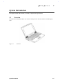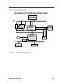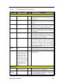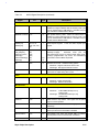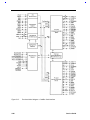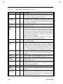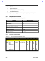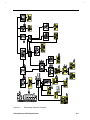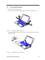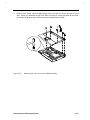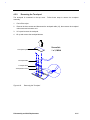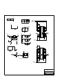
1
TI Extensa 61X Series (AcerNote 370P) Notebook Service Guide PART NO.: 2238309-0809 DOC. NO.: PRINTED IN USA Copyright Copyright © 1997 by Acer Incorporated. All rights reserved. No part of this publication may be reproduced, transmitted, transcribed, stored in a retrieval system, or translated into any language or computer language, in any form or by any means, electronic, mechanical, magnetic, optical, chemical, manual or otherwise, without the prior written permission of Acer Incorporated. Disclaimer Acer Incorporated makes no representations or warranties, either expressed or implied, with respect to the contents hereof and specifically disclaims any warranties of merchantability or fitness for any particular purpose. Any Acer Incorporated software described in this manual is sold or licensed "as is". Should the programs prove defective following their purchase, the buyer (and not Acer Incorporated, its distributor, or its dealer) assumes the entire cost of all necessary servicing, repair, and any incidental or consequential damages resulting from any defect in the software. Further, Acer Incorporated reserves the right to revise this publication and make changes from time to time in the contents hereof without obligation of Acer Incorporated to notify any person of such revision or changes. Acer is a registered trademark of Acer Incorporated. IBM, PS/2 and OS/2 are registered trademarks of International Business Machines Corporation. Intel and Pentium are registered trademarks of Intel Corporation. MS-DOS, Windows and Windows 95 are registered trademarks of Microsoft Corporation. Other brands and product names are trademarks and/or registered trademarks of their respective holders. ii About this Manual Purpose This service guide contains reference information for the Extensa 610 notebook computer. It gives the system and peripheral specifications, shows how to identify and solve system problems and explains the procedure for removing and replacing system components. It also gives information for ordering spare parts. Manual Structure This service guide consists of four chapters and seven appendices as follows: Chapter 1 System Introduction This chapter gives the technical specifications for the notebook and its peripherals. Chapter 2 Major Chip Descriptions This chapter lists the major chips used in the notebook and includes pin descriptions and related diagrams of these chips. Chapter 3 BIOS Setup Information This chapter includes the system BIOS information, focusing on the BIOS setup utility. Chapter 4 Disassembly and Unit Replacement This chapter tells how to disassemble the notebook and replace components. Appendix A Model Number Definition This appendix lists the model number definition of this notebook model series. Appendix B Exploded View Diagram This appendix shows the exploded view diagram of the notebook. Appendix C Spare Parts List This appendix contains spare parts information. Appendix D Schematics This appendix contains the schematic diagrams of the notebook. iii Appendix E BIOS POST Checkpoints This appendix lists all the BIOS POST checkpoints. Appendix F Technical Bulletins and Updates This appendix reserves a space for technical bulletins and future updates. Appendix G Forms This appendix contains standard forms that can help improve customer service. Related product information AcerNote 370P User's Manual contains system description and general operating instructions. M1521, M1523 and M7101 Data Sheets contain information on the Acer chips. C&T 65550 Data Sheet contains detailed information on the Chips & Tech. VGA controller. TI PCI1131 Data Sheet contains detailed information on the Texas Instrument PCMCIA controller. NS87336VJG Data Sheet contains detailed information on the NS super I/O controller. YMF715 Data Sheet contains detailed information on the Yamaha YMF715 audio controller. T62.062.C, T62.061.C, T62.064.C, and T62.066.C Data Sheets contain detailed information on the Ambit components. iv Conventions The following are the conventions used in this manual: Text entered by user Screen messages Represents text input by the user. Denotes actual messages that appear onscreen. NOTE Gives bits and pieces of additional information related to the current topic. WARNING Alerts you to any damage that might result from doing or not doing specific actions. CAUTION Gives precautionary measures to avoid possible hardware or software problems. IMPORTANT Reminds you to do specific actions relevant to the accomplishment of procedures. TIP Tells how to accomplish a procedure with minimum steps through little shortcuts. v vi Table of Contents Chapter 1 1.1 1.2 System Introduction Overview.......................................................................................................................... 1-1 1.1.1 Features ........................................................................................................... 1-2 1.1.2 Rear Ports ........................................................................................................ 1-3 1.1.3 Indicator Light ................................................................................................. 1-4 1.1.4 System Specifications Overview ....................................................................... 1-5 System Board Layout........................................................................................................ 1-7 1.2.1 Main Board (PCB No: 96149-SC) .................................................................... 1-7 1.2.2 Audio Connection Board (PCB No:96467-1).................................................... 1-9 1.2.3 Battery Connection Board (PCB No:95498-1) .................................................. 1-9 1.2.4 HDD Connection Board (PCB No:96463-1) ................................................... 1-10 1.2.5 Keyboard Connection Board (PCB No: 96465-1)............................................ 1-11 1.3 Jumpers and Connectors................................................................................................. 1-12 1.4 Hardware Configuration and Specification ..................................................................... 1-14 1.4.1 Memory Address Map.................................................................................... 1-14 1.4.2 Interrupt Channel Map................................................................................... 1-14 1.4.3 DMA Channel Map ....................................................................................... 1-15 1.4.4 I/O Address Map............................................................................................ 1-15 1.4.5 M7101 GPIO (General Purpose I/O) Port Definition ...................................... 1-16 1.4.6 Processor........................................................................................................ 1-16 1.4.7 BIOS.............................................................................................................. 1-17 1.4.8 System Memory ............................................................................................. 1-17 1.4.9 Second-Level Cache....................................................................................... 1-18 1.4.10 Video Memory ............................................................................................... 1-19 1.4.11 Video ............................................................................................................. 1-19 1.4.11.1 External CRT Resolution Support ............................................... 1-19 1.4.11.2 LCD Resolution Support ............................................................. 1-20 1.4.12 Parallel Port ................................................................................................... 1-21 1.4.13 Serial Port...................................................................................................... 1-21 1.4.14 Audio............................................................................................................. 1-22 1.4.15 PCMCIA........................................................................................................ 1-22 1.4.16 Touchpad ....................................................................................................... 1-23 vii 1.4.17 Keyboard........................................................................................................1-23 1.4.17.1 1.5 1.4.18 FDD ...............................................................................................................1-24 1.4.19 HDD...............................................................................................................1-24 1.4.20 CD-ROM........................................................................................................1-25 1.4.21 Battery............................................................................................................1-25 1.4.22 Charger ..........................................................................................................1-26 1.4.23 DC-DC Converter...........................................................................................1-27 1.4.24 DC-AC Inverter..............................................................................................1-27 1.4.25 LCD ...............................................................................................................1-28 1.4.26 AC Adapter ....................................................................................................1-29 Software Configuration and Specification .......................................................................1-30 1.5.1 1.5.2 BIOS ..............................................................................................................1-30 1.5.1.1 Keyboard Hotkey Definition.........................................................1-30 1.5.1.2 MultiBoot ....................................................................................1-31 1.5.1.3 Power Management .....................................................................1-31 Drivers, Applications and Utilities..................................................................1-36 1.6 System Block Diagram ...................................................................................................1-38 1.7 Environmental Requirements..........................................................................................1-39 1.8 Mechanical Specifications ..............................................................................................1-40 Chapter 2 Major Chips Description 2.1 Major Component List......................................................................................................2-1 2.2 ALI M1521 ......................................................................................................................2-2 2.3 viii Windows 95 Keys ........................................................................1-23 2.2.1 Features............................................................................................................2-2 2.2.2 Block Diagram .................................................................................................2-4 2.2.3 System Architecture .........................................................................................2-5 2.2.4 Data Path .........................................................................................................2-6 2.2.5 Pin Diagram .....................................................................................................2-7 2.2.6 Signal Descriptions ..........................................................................................2-8 ALI M1523 ....................................................................................................................2-14 2.3.1 Features..........................................................................................................2-14 2.3.2 Block Diagram ...............................................................................................2-16 2.3.3 Pin Diagram ...................................................................................................2-17 2.3.4 Signal Descriptions ........................................................................................2-18 2.4 2.5 2.6 2.7 2.8 2.9 ALI M7101 (Power Management Unit) .......................................................................... 2-24 2.4.1 Features ......................................................................................................... 2-24 2.4.2 Pin Diagram................................................................................................... 2-25 2.4.3 Pin Description .............................................................................................. 2-26 2.4.4 Different Pin definition setting ....................................................................... 2-34 2.4.5 Numerical Pin List ......................................................................................... 2-36 2.4.6 Alphabetical Pin List...................................................................................... 2-37 2.4.7 Function Description...................................................................................... 2-38 C&T 65550 High Performance Flat Panel/CRT VGA Controller.................................... 2-40 2.5.1 Features ......................................................................................................... 2-40 2.5.2 Block Diagram............................................................................................... 2-41 2.5.3 Pin Diagram................................................................................................... 2-42 2.5.4 Pin Descriptions............................................................................................. 2-43 TI PCI1131 CardBus Controller ..................................................................................... 2-56 2.6.1 Overview........................................................................................................ 2-56 2.6.2 Architecture ................................................................................................... 2-57 2.6.3 Features ......................................................................................................... 2-57 2.6.4 Block Diagram............................................................................................... 2-59 2.6.5 Pin Diagram................................................................................................... 2-61 2.6.6 Terminal Functions........................................................................................ 2-63 NS87336VJG Super I/O Controller ................................................................................ 2-75 2.7.1 Features ......................................................................................................... 2-75 2.7.2 Block Diagram............................................................................................... 2-77 2.7.3 Pin Diagram................................................................................................... 2-78 2.7.4 Pin Description .............................................................................................. 2-79 Yamaha YMF715 Audio Chip........................................................................................ 2-87 2.8.1 Features ......................................................................................................... 2-87 2.8.2 Pin Diagram................................................................................................... 2-88 2.8.3 Pin Descriptions............................................................................................. 2-89 T62.062.C Battery Charger ............................................................................................ 2-91 2.9.1 Overview........................................................................................................ 2-91 2.9.2 Features ......................................................................................................... 2-91 2.9.3 Absolute Maximum Ratings ........................................................................... 2-92 2.9.4 Electrical Characteristics................................................................................ 2-92 ix 2.10 2.11 2.12 2.9.5 Pin Diagram ...................................................................................................2-94 2.9.6 Pin Description...............................................................................................2-95 2.9.7 Functions Description.....................................................................................2-96 Charge Function ..........................................................................2-96 2.9.7.2 Discharge Function......................................................................2-96 2.9.7.3 Safety Concerns...........................................................................2-97 T62.061.C DC-DC Converter .........................................................................................2-98 2.10.1 Pin Diagram ...................................................................................................2-98 2.10.2 Pin Assignment ..............................................................................................2-98 2.10.3 Specifications .................................................................................................2-99 2.10.4 Control.........................................................................................................2-100 2.10.5 Application: .................................................................................................2-100 T62.064.C DC-AC Inverter (11.3”) ..............................................................................2-102 2.11.1 Electrical Specifications ...............................................................................2-102 2.11.2 Pin & Connector Assignment .......................................................................2-103 2.11.3 Top Overlay .................................................................................................2-104 2.11.4 Bottom Overlay ............................................................................................2-104 T62.066.C DC-AC Inverter (12.1”) ..............................................................................2-105 2.12.1 Electrical Specifications ...............................................................................2-105 2.12.2 Pin & Connector Assignment .......................................................................2-106 2.12.3 Top Overlay .................................................................................................2-107 2.12.4 Bottom Overlay ............................................................................................2-107 Chapter 3 x 2.9.7.1 BIOS Setup Information 3.1 When to Use Setup ...........................................................................................................3-1 3.2 Entering Setup..................................................................................................................3-2 3.3 Basic System Configuration..............................................................................................3-4 3.3.1 Date and Time..................................................................................................3-4 3.3.2 Floppy Disk Drives...........................................................................................3-4 3.3.3 Hard Disk Drive ...............................................................................................3-4 3.3.4 Large Hard Disk Capacity ................................................................................3-4 3.3.5 Memory Test ....................................................................................................3-5 3.3.6 Boot Display.....................................................................................................3-5 3.3.7 Quiet Boot ........................................................................................................3-5 3.4 3.5 System Security................................................................................................................ 3-6 3.4.1 Floppy Disk Drive Control ............................................................................... 3-6 3.4.2 Hard Disk Drive Control .................................................................................. 3-6 3.4.3 System Boot Drive Control............................................................................... 3-7 3.4.4 CD-ROM Bootable........................................................................................... 3-7 3.4.5 Serial Port 1 Base Address ............................................................................... 3-8 3.4.6 Parallel Port Base Address ............................................................................... 3-8 3.4.7 Parallel Port Operation Mode ........................................................................... 3-8 3.4.8 Passwords ........................................................................................................ 3-9 3.4.9 CardBus Support............................................................................................ 3-10 Power Management Settings .......................................................................................... 3-11 3.5.1 Power Management Mode.............................................................................. 3-11 3.5.2 Display Standby Timer................................................................................... 3-11 3.5.3 Hard Disk Standby Timer............................................................................... 3-11 3.5.4 System Sleep Timer ....................................................................................... 3-12 3.5.5 System Sleep Mode ........................................................................................ 3-12 3.5.6 System Resume Timer Mode .......................................................................... 3-12 3.5.7 System Resume Date and Time ...................................................................... 3-12 3.5.8 Modem Ring Resume On Indicator ................................................................ 3-12 3.5.9 Battery-low Warning Beep ............................................................................. 3-13 3.5.10 Sleep Upon Battery-low.................................................................................. 3-13 3.6 System Information Reference........................................................................................ 3-14 3.7 Load Setup Default Settings ........................................................................................... 3-16 Chapter 4 4.1 Disassembly and Unit Replacement General Information......................................................................................................... 4-2 4.1.1 Before You Begin............................................................................................. 4-2 4.1.2 Connector Types .............................................................................................. 4-3 4.1.3 Disassembly Sequence...................................................................................... 4-4 4.2 Replacing Memory ........................................................................................................... 4-6 4.3 Removing the Hard Disk Drive ........................................................................................ 4-7 4.4 Removing the Keyboard ................................................................................................... 4-9 xi 4.5 4.6 Disassembling the Inside Frame Assembly .....................................................................4-10 4.5.1 Removing the Heat Sink Assembly .................................................................4-10 4.5.2 Removing the Internal Drive ..........................................................................4-11 4.5.3 Replacing the CPU .........................................................................................4-12 4.5.4 Removing the Display ....................................................................................4-13 4.5.5 Detaching the Top Cover................................................................................4-14 4.5.6 Removing the Base Assembly .........................................................................4-16 4.5.7 Removing the Motherboard ............................................................................4-17 4.5.8 Disassembling the Motherboard......................................................................4-20 4.5.9 Removing the Touchpad.................................................................................4-21 Disassembling the Display..............................................................................................4-22 Appendix A Model Number Definition Appendix B Exploded View Diagram Appendix C Spare Parts List Appendix D Schematics Appendix E BIOS POST Checkpoints Appendix F Technical Bulletins and Updates Appendix G Forms xii List of Figures 1-1 Notebook.......................................................................................................................... 1-1 1-2 Rear Ports ........................................................................................................................ 1-3 1-3 Indicator Light ................................................................................................................. 1-4 1-4 Main Board Layout (Top Side) ......................................................................................... 1-7 1-5 Main Board Layout (Bottom Side).................................................................................... 1-8 1-6 Audio Connection Board Layout (Top Side) ..................................................................... 1-9 1-7 Battery Connection Board Layout (Top Side) ................................................................... 1-9 1-8 Battery Connection Board Layout (Bottom Side) .............................................................. 1-9 1-9 HDD Connection Board Layout (Top Side) .................................................................... 1-10 1-10 HDD Connection Board Layout (Bottom Side) ............................................................... 1-10 1-11 Keyboard Connection Board Layout (Top Side).............................................................. 1-11 1-12 Keyboard Connection Board Layout (Bottom Side)......................................................... 1-11 1-13 Jumpers and Connectors (Top View).............................................................................. 1-12 1-14 Power Management Block Diagram ............................................................................... 1-31 1-15 System Block Diagram................................................................................................... 1-38 2-1 Alladin III Block Diagram ............................................................................................... 2-4 2-2 Alladin III System Architecture........................................................................................ 2-5 2-3 M1521 Data Path ............................................................................................................. 2-6 2-4 M1521 Pin Diagram......................................................................................................... 2-7 2-5 M1523 Block Diagram................................................................................................... 2-16 2-6 M1523 Pin Diagram....................................................................................................... 2-17 2-7 M7101 Pin Diagram...................................................................................................... 2-25 2-8 State Machine for PCI Interface ..................................................................................... 2-39 2-9 C&T 65550 Block Diagram............................................................................................ 2-41 2-10 C&T 65550 Pin Diagram ............................................................................................... 2-42 2-11 Functional Block Diagram - 16-bit PC Card Interface .................................................... 2-59 2-12 Functional block diagram - CardBus Card Interface ....................................................... 2-60 2-13 PCI-to-PC Card (16-bit) terminal assignments ............................................................... 2-61 xiii xiv 2-14 PCI-to-CardBus terminal assignments ............................................................................2-62 2-15 NS87336VJG Block Diagram .........................................................................................2-77 2-16 NS87336VJG Pin Diagram.............................................................................................2-78 2-17 YMF715 Block Diagram ................................................................................................2-88 2-18 T62.062.C Pin Diagram..................................................................................................2-94 2-19 T62.061.C Pin Diagram..................................................................................................2-98 2-20 T62.064.C DC-AC Inverter Top Overlay diagram ........................................................2-104 2-21 T62.064.C DC-AC Inverter Bottom Overlay diagram ...................................................2-104 2-22 T62.066.C DC-AC Inverter Top Overlay diagram ........................................................2-107 2-23 T62.066.C DC-AC Inverter Bottom Overlay diagram ...................................................2-107 4-1 Removing the Battery Pack...............................................................................................4-2 4-2 Using Connectors With Locks ..........................................................................................4-3 4-3 Disassembly Sequence Flowchart......................................................................................4-5 4-4 Removing the Memory Door.............................................................................................4-6 4-5 Installing and Removing Memory.....................................................................................4-6 4-6 Removing the Hard Disk Drive Bay Cover........................................................................4-7 4-7 Removing the Hard Disk Drive.........................................................................................4-8 4-8 Removing the Display Hinge Covers.................................................................................4-9 4-9 Unplugging the Keyboard Connectors...............................................................................4-9 4-10 Removing the Heat Sink Assembly Screws .....................................................................4-10 4-11 Removing the Internal Drive ..........................................................................................4-11 4-12 Replacing the CPU .........................................................................................................4-12 4-13 Unplugging the Display Cable ........................................................................................4-13 4-14 Removing the Display Hinge Screws ..............................................................................4-13 4-15 Removing the Bottom Screws .........................................................................................4-14 4-16 Detaching the Top Cover from the Base Assembly..........................................................4-15 4-17 Detaching the Base Assembly .........................................................................................4-16 4-18 Removing the Fan ..........................................................................................................4-17 4-19 Removing the Audio Board.............................................................................................4-17 4-20 Removing the Battery Connector Board.......................................................................... 4-18 4-21 Unplugging the LCD Cover Switch and Speaker Cables................................................. 4-18 4-22 Removing the Charger Board ......................................................................................... 4-19 4-23 Detaching the Motherboard from the Inside Assembly Frame......................................... 4-19 4-24 Removing the PC Card Slot Unit.................................................................................... 4-20 4-25 Removing the Keyboard Connection Board .................................................................... 4-20 4-26 Removing the Touchpad................................................................................................. 4-21 4-27 Removing the LCD Bumpers.......................................................................................... 4-22 4-28 Removing the Display Bezel Screws............................................................................... 4-22 4-29 Removing the Display Bezel........................................................................................... 4-23 4-30 Removing the Hinge Cable Cover................................................................................... 4-23 4-31 Removing the LCD Panel............................................................................................... 4-24 4-32 Removing the LCD ........................................................................................................ 4-24 4-33 Removing the DC-AC Inverter and LCD ID Inverter Boards.......................................... 4-25 4-34 Removing the Display Cable Assembly .......................................................................... 4-25 xv List of Tables xvi 1-1 Port Descriptions .............................................................................................................1-3 1-2 Indicator Status Descriptions ............................................................................................1-4 1-3 System Specifications .......................................................................................................1-5 1-3 System Specifications (continued).....................................................................................1-6 1-4 CPU Voltage (S1) Settings..............................................................................................1-13 1-5 CPU Speed (SW3) Settings.............................................................................................1-13 1-6 Multi-Function Switch (SW2) Settings ...........................................................................1-13 1-7 Memory Address Map ....................................................................................................1-14 1-8 Interrupt Channel Map ...................................................................................................1-14 1-9 DMA Channel Map........................................................................................................1-15 1-10 I/O Address Map ............................................................................................................1-15 1-11 M7101 GPIO Port Definition..........................................................................................1-16 1-12 Processor Specifications..................................................................................................1-16 1-13 BIOS Specifications........................................................................................................1-17 1-14 Memory Configurations..................................................................................................1-18 1-15 Video RAM Configuration .............................................................................................1-19 1-16 Video Hardware Specification.........................................................................................1-19 1-17 Supported External CRT Resolutions..............................................................................1-19 1-18 Supported LCD Resolutions............................................................................................1-20 1-19 Parallel Port Configurations............................................................................................1-21 1-20 Serial Port Configurations ..............................................................................................1-21 1-21 Audio Specifications.......................................................................................................1-22 1-22 PCMCIA Specifications..................................................................................................1-22 1-23 Touchpad Specifications .................................................................................................1-23 1-24 Keyboard Specifications..................................................................................................1-23 1-25 Windows 95 Key Descriptions ........................................................................................1-23 1-26 FDD Specifications.........................................................................................................1-24 1-27 HDD Specifications ........................................................................................................1-24 1-28 CD-ROM Specifications................................................................................................. 1-25 1-29 Battery Specifications..................................................................................................... 1-25 1-30 Charger Specifications ................................................................................................... 1-26 1-31 DC-DC Converter Specifications.................................................................................... 1-27 1-32 DC-AC Inverter Specifications....................................................................................... 1-27 1-33 LCD Specifications ........................................................................................................ 1-28 1-34 AC Adapter Specifications ............................................................................................. 1-29 1-35 Hotkey Descriptions ....................................................................................................... 1-30 1-36 Standby Mode Conditions and Descriptions.................................................................... 1-32 1-37 Suspend Mode Conditions and Descriptions ................................................................... 1-34 1-38 Display Standby Mode Conditions and Descriptions....................................................... 1-34 1-39 Hard Disk Standby Mode Conditions and Descriptions................................................... 1-35 1-40 Location of Drivers in the System Utility CD.................................................................. 1-36 1-41 Location of Applications in the System Utility CD ......................................................... 1-36 1-42 Environmental Requirements ......................................................................................... 1-38 1-43 Mechanical Specifications .............................................................................................. 1-39 2-1 Major Chips List .............................................................................................................. 2-1 2-2 M1521 Signal Descriptions .............................................................................................. 2-8 2-3 M1523 Signal Descriptions ............................................................................................ 2-18 2-4 M7101 Pin Descriptions................................................................................................. 2-26 2-5 M7101 Different Pin Definition Setting.......................................................................... 2-34 2-6 M7101 Original Pin Definition Setting........................................................................... 2-35 2-7 M7101 Numerical Pin List ............................................................................................. 2-36 2-8 M7101 Alphabetical Pin List.......................................................................................... 2-37 2-9 M7101 PCI Interface Lock Register................................................................................ 2-39 2-10 C&T 65550 Pin Descriptions.......................................................................................... 2-43 2-11 Flat Panel Display Interface Configurations.................................................................... 2-54 2-12 Bus Output Signal Status During Standby Mode............................................................. 2-55 2-13 PCI1131 Pin Descriptions .............................................................................................. 2-63 xvii 2-14 NS87336VJG Pin Descriptions .......................................................................................2-79 2-15 YMF715 Descriptions.....................................................................................................2-89 2-16 T62.062.C Absolute Maximum Ratings Table ................................................................2-92 2-17 T62.062.C Electrical Characteristics Table .....................................................................2-92 2-18 T62.062.C Pin Description table.....................................................................................2-95 2-19 T62.061.C Pin Descriptions............................................................................................2-98 2-20 MAXIMUM RATINGS................................................................................................2-102 2-21 Electrical Characteristics ..............................................................................................2-102 2-22 Pin Description.............................................................................................................2-103 2-23 Pin Description.............................................................................................................2-103 2-24 MAXIMUM RATINGS................................................................................................2-105 2-25 Electrical Characteristics ..............................................................................................2-105 2-26 J1: 52103-1217 (MOLEX) Pin Description..................................................................2-106 2-27 J2:SM02(8.0)B-BHS-1-TB2P (JST) Pin Description .....................................................2-106 3-1 Display Device Settings ....................................................................................................3-5 3-2 Floppy Disk Drive Control Settings ..................................................................................3-6 3-3 Hard Disk Drive Control Settings .....................................................................................3-6 3-4 System Boot Drive Control Settings..................................................................................3-7 3-5 CD-ROM Image Descriptions...........................................................................................3-7 3-6 System Status Descriptions .............................................................................................3-15 4-1 Guide to Disassembly Sequence........................................................................................4-4 C-1 Spare Parts List ............................................................................................................... C-1 E-1 POST Checkpoint List..................................................................................................... E-1 xviii C h a p t e r 1 System Introduction This chapter introduces the notebook, its features, components and specifications. 1.1 Overview The notebook was designed with the user in mind. The figure below shows the notebook with the display open. Figure 1-1 Notebook System Introduction 1-1 1.1.1 Features Here are just a few of the notebook’s many features: Performance • High-end Pentium microprocessor • Support 64-bit main memory and external (L2) cache memory • Large LCD display (DualScan STN and TFT active matrix.) • PCI local bus video with graphics acceleration and 1MB video RAM boost video performance • Internal 3.5-inch floppy drive or CD-ROM drive • High-capacity, Enhanced-IDE hard disk • Lithium-Ion or Nickel Metal-Hydride battery pack • Power management system with standby and hibernation power saving modes Multimedia • 16-bit stereo audio with software wavetable • Built-in dual speakers • Ultra-slim, high-speed CD-ROM drive1 Human-centric Design and Ergonomics • Lightweight and slim • Sleek, smooth and stylish design • Full-sized keyboard • Wide and curved palm rest • Centrally-located touchpad pointing device Expansion • PC card (formerly PCMCIA) slots (two type II/I or one type III) with ZV (Zoomed Video) port support • Upgradeable memory, hard disk, CPU 1 Some areas or regions may not offer models with a built-in CD-ROM drive. 1-2 Service Guide 1.1.2 1 2 3 4 5 Rear Ports DC-in Port Microphone-in Port Line-in Port Line-out Port External Floppy Drive Connector 6 7 8 9 Serial Port Parallel Port External CRT Port PS/2 Port Figure 1-2 Rear Ports The following table describes these ports. Table 1-1 Port Descriptions # Icon Port Connects to... 1 DC-in Port AC adapter and power outlet 2 Microphone-in Port External 3.5mm minijack condenser microphone 3 Line-in Port Line-in device (e.g., CD player, stereo walkman) 4 Line-out Port Line-out device (e.g., speakers, headphones) 5 External Floppy Drive Connector External floppy drive 6 Serial Port Serial device (e.g., serial mouse) 7 Parallel Port Parallel device (e.g., parallel printer) 8 External CRT port Monitor (up to 1024x768, 256-colors ) 9 PS/2 Port PS/2-compatible device (e.g., PS/2 keyboard, keypad, mouse) 1.1.3 Indicator Light A two-way indicator light is found on the inside and outside of the display. See figure below. System Introduction 1-3 Indicator Light Indicator Light Figure 1-3 Indicator Light This two-way indicator light allows you to see the notebook status when the display is open or closed. The indicator serves both as a power and battery-charging indicator. See Table 1-2. Table 1-2 Indicator Status Descriptions Indicator Status Power Switch Condition Green On Charged battery is installed or a power AC adapter is connected to the notebook. Red Off Battery is installed and a powered AC adapter is connected to the notebook and charging the battery (rapid charge mode). Orange On Battery is installed and a powered AC adapter is connected to the notebook and charging the battery (charge-in-use mode). Flashing On Battery is running low on power and no AC adapter is connected to the notebook. 1-4 Service Guide 1.1.4 System Specifications Overview Table 1-3 System Specifications Item Standard Optional Microprocessor Intel Pentium™ processor (Intel P54CSLM 120/133/150 MHz) Intel P55CLM - 133/150 with MMX System memory 8MB / 16MB Dual 64-bit memory banks Expandable to 64MB using 8, 16 and 32MB soDIMMs Flash ROM BIOS 256KB Data storage devices Removable 12.5mm, 2.5-inch, 1.0GB Enhanced-IDE hard disk 1+GB Enhanced-IDE hard disk drive CD-ROM model Internal 15mm, 5.25-inch high-speed CD-ROM drive External 3.5-inch, 1.44MB diskette drive FDD model Internal 3.5-inch, 1.44MB floppy drive Display DualScan STN or TFT active matrix, 800x600, 256 colors (SVGA) Up to 1024x768, 256-color ultra-VGA monitor LCD projection panel Video PCI local bus video with graphics accelerator and 1MB video RAM Audio 16-bit stereo audio; built-in dual speakers; separate audio ports Keyboard and pointing device 84-/85-/88-key with Windows 95 keys 101-/102-key, PS/2-compatible keyboard or 17-key numeric keypad Touchpad (centrally-located on palmrest) External serial or PS/2 mouse or similar pointing device One 9-pin RS-232 serial port (UART16550-compatible) Serial mouse, printer or other serial devices I/O ports Parallel printer or other parallel devices One 25-pin parallel port (EPP/ECP-compliant) One 15-pin CRT port One 6-pin PS/2 keypad/ keyboard/mouse connector Up to a 1024x768, 256-color ultra-VGA monitor 17-key numeric keypad, PS/2 keyboard or mouse LAN card or other PC cards One type III or two type II PC Card slot(s) with ZV port support External diskette drive One external FDD port System Introduction 1-5 Table 1-3 System Specifications (continued) Item I/O ports (continued) Standard Optional One 3.5mm minijack mic-in port Microphone One 3.5mm minijack line-in port Audio CD player or other line-in devices One 3.5mm minijack line-out port Speakers or headphones Operating system Windows 95 Windows 3.1 Weight FDD model CD-ROM model (includes battery) 2.6 kg. (5.7 lbs.) 2.8 kg. (6.2 lbs.) Dimensions (main footprint) WxDxH 306mm x 228mm x 46mm (12.05” x 8.98” x 1.81”) Temperature Operating Non-operating 10ºC ~ 35ºC -20ºC ~ 60ºC Humidity Operating Non-operating (non-condensing) 20% ~ 80% 20% ~ 80% AC adapter 100~240 Vac, 50~60 Hz, 45W autosensing AC adapter Extra AC adapter 4-5 hr. (rapid-charge) Extra battery pack External battery charger/discharger Battery pack Lithium-Ion 6-8 hr. (charge-in-use) Nickel Metal-Hydride battery 1-6 2-2.5 hr. (rapid-charge) 5.5-6.5 hr. (charge-in-use) Extra battery pack External battery charger/discharger Service Guide 1.2 System Board Layout 1.2.1 Main Board (PCB No: 96149-SC) Note: This switch setting is not for Extensa 610 use. Figure 1-4 Main Board Layout (Top Side) System Introduction 1-7 Figure 1-5 1-8 Main Board Layout (Bottom Side) Service Guide 1.2.2 Figure 1-6 1.2.3 Audio Connection Board (PCB No:96467-1) Audio Connection Board Layout (Top Side) Battery Connection Board (PCB No:95498-1) Figure 1-7 Battery Connection Board Layout (Top Side) Figure 1-8 Battery Connection Board Layout (Bottom Side) System Introduction 1-9 1.2.4 HDD Connection Board (PCB No:96463-1) Figure 1-9 HDD Connection Board Layout (Top Side) Figure 1-10 HDD Connection Board Layout (Bottom Side) 1-10 Service Guide 1.2.5 Keyboard Connection Board (PCB No: 96465-1) Figure 1-11 Keyboard Connection Board Layout (Top Side) Figure 1-12 Keyboard Connection Board Layout (Bottom Side) System Introduction 1-11 1.3 Jumpers and Connectors CN7 CN1 CN2 CN8 CN9 CN3 CN10 CN4 CN5 CN11 CN6 CN12 CN13 CN14 CN15 CN17 CN16 SW3 SW2 CN18 CN19 S1 Golden Finger for Debug Card NOTE: The shaded area (Black) indicates the position of the switch. CN1 CN2 CN3 CN4 CN5 CN6 CN7 CN8 CN9 CN10 CN11 External PS/2 keyboard/mouse port VGA port Parallel port Serial port External floppy drive port LCD Connector Audio speaker connector (left) LCD cover switch connector Fan connector Audio speaker connector (right) Charger Connector Figure 1-13 1-12 CN12 CN13 CN14 CN15 CN16 CN17 CN18 CN19 S1 SW2 SW3 Audio Board Connector PCMCIA socket connector Diskette Drive connector HDD Connector Keyboard connector CD-ROM connector Battery pack connector Track Point Board Connector CPU Voltage Setting Function Setting CPU Speed Setting Jumpers and Connectors (Top View) Service Guide Table 1-4 CPU Voltage (S1) Settings CPU Voltage 2.35V 2.45V 2.9V 3.1V Switch 1 Off Off Off Off Switch 2 Off On Off Off Switch 3 On Off Off Off Switch 4 Off Off Off On Table 1-5 CPU Speed (SW3) Settings CPU Speed 120MHz 133MHz 150MHz Switch 1 Off On Off Switch 2 On Off On Switch 3 Off Off On Switch 4 On On On ON OFF Table 1-6 Multi-Function Switch (SW2) Settings Switch 1 Keyboard Type (Default OFF) - - 2 Keyboard Type 88-key (Japan keyboard) 84/85-key (U.S. keyboard) 3 Password Bypass Check 4 Generic boot-up screen show on screen in POST No Yes System Introduction 1-13 1.4 Hardware Configuration and Specification 1.4.1 Memory Address Map Table 1-7 Memory Address Map Address Range Definition Function 000000 - 09FFFF 640 KB memory Base memory 0A0000 - 0BFFFF 128 KB video RAM Reserved for graphics display buffer 0C0000 - 0CBFFF Video BIOS Video BIOS 0E0000 - 0EFFFF 128 KB system BIOS System BIOS 0F0000 - 0FFFFF System BIOS 10000 - 7FFFF 80000 - 27FFF Extended memory Onboard Memory SIMM memory FE0000 - FFFFFF 256 KB system ROM Duplicate of code assignment at 0E0000-0FFFFF 1.4.2 Interrupt Channel Map Table 1-8 Interrupt Channel Map Priority Interrupt Number 1 2 3 4 SMI NMI IRQ 0 IRQ 1 IRQ 2 IRQ 8 IRQ 9 IRQ 10 IRQ 11 IRQ 12 IRQ 13 IRQ 14 IRQ 15 IRQ 3 IRQ 4 IRQ 5 IRQ 6 IRQ 7 5 6 7 8 9 10 11 12 13 14 15 16 17 Interrupt Source Power management unit Parity error detected, I/O channel error Interval timer, counter 0 output Keyboard Interrupt from controller 2 (cascade) Real-time clock Cascaded to INT 0AH (IRQ 2) Audio (option) / PCMCIA Audio (option) / PCMCIA PS/2 mouse INT from coprocessor Hard disk controller CD-ROM controller Serial communication port 2 Serial communication port 1 Parallel port (option) / Audio Diskette controller Parallel port (option) A PCMCIA card can use IRQ 3, 4, 5, 7, 9 and 11 as long as it does not conflict with the interrupt address of any other device. 1.4.3 DMA Channel Map Table 1-9 1-14 DMA Channel Map Controller Channel Address Function 1 0 0087 Audio (option)/ECP(option) Service Guide 1 2 3 4 5 6 7 1 1 1 2 2 2 2 1.4.4 0083 0081 0082 Cascade 008B 0089 008A Audio Diskette Audio (option)/ECP(option) Cascade Spare - I/O Address Map Table 1-10 I/O Address Map Address Range 000 - 00F 020 - 021 040 - 043 048 - 04B 060 - 064 070 - 071 080 - 08F 0A0 - 0A1 0C0 - 0DF 170 - 177 178, 17A 1F0 - 1F7 3F6, 3F7 220 - 22F, 240 - 24F 300 - 301, 330 - 331 370 - 371, 388 - 38F 530 - 537, E80 - E89 278 - 27F 2E8 - 2EF 2F8 - 2FF 378, 37A 3BC - 3BE 3B4, 3B5, 3BA 3C0 - 3C5 3C6 - 3C9 3C0 - 3CF 3D0 - 3DF 3E0 - 3E1 3E8 - 3EF 3F0 - 3F7 3F8 - 3FF CF8 - CFF System Introduction Device DMA controller-1 Interrupt controller-1 Timer 1 Timer 2 Keyboard controller 38802 chip select Real-time clock and NMI mask DMA page register Interrupt controller-2 DMA controller-2 CD-ROM M7101 registers Hard disk select Audio (option) - default Audio (option) Audio (option) Audio (option) Parallel port 3 COM 4 COM 2 Parallel port 2 Parallel port 1 Video subsystem Video DAC Enhanced graphics display Color graphics adapter PCMCIA controller COM3 Floppy disk controller COM 1 PCI configuration register 1-15 1.4.5 M7101 GPIO (General Purpose I/O) Port Definition Table 1-11 M7101 GPIO Port Definition Item Description GPIOA2 Smart inverter contrast counter control GPIOA3 0: Normal operation of system 1: Shutdown system GPIOA4 Serial data on X24C02 GPIOA5 Battery gauge communication control GPIOA6 Battery data line GPIOA7 Thermal sensor data line GPIOC6 VGA thermal sensor data line GPIOC7 0: VGA chip standby mode 1: Normal operation Register E0h bit 8 Serial clock on X24C02 Register E0h bit 9 0: Disable 12V for flash ROM 1: Enable 12V for flash ROM Register E0h bit 10 0: 3 mode FDD 1: Normal Register E0h bit 11 Thermal sensor clock line Register E0h bit 12 Thermal sensor reset Register E0h bit 13 0: Enable battery LED 1: Disable battery LED Register E0h bit 14 0: Disable audio amplifier 1: Enable audio amplifier Register E1h bit 0 0: NiMH battery 1: Li-ion battery Register E1h bit 1 1.4.6 CPU thermal high Processor Table 1-12 Processor Specifications Item Specification CPU type P54CSLM-120,P54CSLM-133, P54CSLM-150, P55CLM-133, P55CLM - 150 CPU package SPGA Switchable processor speed (Y/N) Yes Minimum working speed 0MHz while hibernation mode CPU voltage 3.1V/2.9V/2.45V 1.4.7 Table 1-13 1-16 BIOS BIOS Specifications Service Guide Item Specification BIOS vendor Acer BIOS version v2.1 BIOS in flash EPROM (Y/N) Yes BIOS ROM size 256KB BIOS package type 32-pin TSOP Same BIOS for STN color/TFT color (Y/N) Yes The BIOS can be overwritten/upgradeable using the “AFLASH” utility (AFLASH.EXE). Please refer to software specification section for details. 1.4.8 System Memory Memory is upgradeable from 8 to 64 MB, employing 8-/16-/32-MB 64-bit soDIMMs (Small Outline Dual Inline Memory Modules). After installing the memory modules, the system automatically detects and reconfigures the total memory size during the POST routines. The following lists important memory specifications. • Memory bus width: 64-bit • Expansion RAM module type:144-pin, 64-bit, small outline Dual Inline Memory Module (soDIMM) • Expansion RAM module size/configuration: • 8MB (1M*16 x4) • 16MB (2M*8 x8) • 32MB (4M*16 x4) • Expansion RAM module speed/voltage/package: 60ns/3.3v/TSOP EDO • EDO and fast-page mode DIMMs may be used together in a memory configuration. System Introduction 1-17 The following table lists all possible memory configurations. Table 1-14 Memory Configurations 1.4.9 Slot 1 Slot 2 Total Memory 8 MB 0 MB 8 MB 0 MB 8 MB 8 MB 8 MB 8 MB 16 MB 16 MB 0 MB 16 MB 0 MB 16 MB 16 MB 16 MB 8 MB 24 MB 8 MB 16 MB 24 MB 16 MB 16 MB 32 MB 32 MB 0 MB 32 MB 0 MB 32 MB 32 MB 32 MB 8 MB 40 MB 8 MB 32 MB 40 MB 32 MB 16 MB 48 MB 16 MB 32 MB 48 MB 32 MB 32 MB 64 MB Second-Level Cache This notebook supports 256KB pipeline burst second-level (L2) cache. 1-18 Service Guide 1.4.10 Video Memory Table 1-15 Video RAM Configuration Item Specification DRAM or VRAM DRAM(EDO type) Fixed or upgradeable Fixed Memory size/configuration 1MB (256K x 16 x 2pcs) Memory speed 60ns Memory voltage 3.3V Memory package TSOP 1.4.11 Video Table 1-16 Video Hardware Specification Item Specification Video chip C&T65550B Working voltage C&T65550B: 3.3V C&T65550XX: 3.3V/5V (“XX” represents codes other than “A” (i.e. “B1”)) Video Chip substitutability Yes During power-on, system supplies 5V to video chip and read its register to determine whether the video chip is 5V or 3.3V/5V type. If 5V video chip is detected, system maintains video voltage at 5V; if 3.3V/5V video chip is detected, system switches video voltage to 3.3V. 1.4.11.1 External CRT Resolution Support Table 1-17 Supported External CRT Resolutions Resolution x Color on External CRT CRT Refresh Rate Simultaneous on TFT LCD Simultaneous on STN LCD CRT only Simultaneous SVGA SVGA 640x480x16 60,75,85 60 Y Y 640x480x256 60,75,85 60 Y Y 640x480x65,536 60,75,85 60 Y Y 640x480x16,777,216 60,75,85 60 Y N 800x600x16 56,60,75 60 Y Y 800x600x256 56,60,75 60 Y Y 56,60 60 Y N 60,75,86I 60 Y Y Simultaneous on TFT LCD Simultaneous on STN LCD Y Y 800x600x65,536 1024x768x16 Table 1-17 Supported External CRT Resolutions (Continued) Resolution x Color on External CRT 1024x768x256 System Introduction CRT Refresh Rate 60,75,86I 60 1-19 1280x1024x16 86I 60 Y Y 1.4.11.2 LCD Resolution Support Table 1-18 Supported LCD Resolutions Resolution x Color on LCD Only TFT LCD (SVGA) STN LCD (SVGA) 640x480x16 Y Y 640x480x256 Y Y 640x480x65,536 Y Y 640x480x16,777,216 Y - 800x600x16 Y Y 800x600x256 Y Y 800x600x65,536 Y - 1024x768x16 Y Y 1024x768x256 Y Y • DSTN color number: 256 colors • TFT color number: 65536 colors • Maximum resolution (LCD Panel): 800x600 • Maximum resolution (External CRT): 1280x1024 Using software, you can set the LCD to a higher resolution than its physical resolution, but the image shown on the LCD will pan. 1-20 Service Guide 1.4.12 Parallel Port Table 1-19 Parallel Port Configurations Item Specification Number of parallel ports 1 ECP/EPP support Yes (set by BIOS setup) Connector type 25-pin D-type Location Rear side Selectable parallel port (by BIOS Setup) • • • • 1.4.13 Parallel 1 (3BCh, IRQ7) Parallel 2 (378h, IRQ7) Parallel 3 (278h, IRQ5) Disable Serial Port Table 1-20 Serial Port Configurations Item Specification Number of serial ports 1 16550 UART support Yes Connector type 9-pin D-type Location Rear side Selectable serial port (by BIOS Setup) • • • System Introduction Serial 1 (3F8h, IRQ4) Serial 2 (2F8h, IRQ3) Disable 1-21 1.4.14 Audio Table 1-21 Audio Specifications Item Specification Chipset YMF715 Audio onboard or optional Built-in Mono or stereo Stereo Resolution 16-bit Compatibility SB-16 , Windows Sound System Mixed sound sources Voice, Synthesizer, Line-in, Microphone, CD Voice channel 8-/16-bit, mono/stereo Sampling rate 44.1 kHz Internal microphone No Internal speaker / quantity Yes / 2 pcs. Microphone jack Yes Headphone jack Yes 1.4.15 PCMCIA PCMCIA is an acronym for Personal Computer Memory Card International Association. The PCMCIA committee set out to standardize a way to add credit-card size peripheral devices to a wide range of personal computers with as little effort as possible. There are two type II/I or one type III PC Card slots found on the left panel of the notebook. These slots accept credit-card-sized cards that enhances the usability and expandability of the notebook. ZV (Zoomed Video) port support allows your system to support hardware MPEG in the form of a ZV PC card. Table 1-22 PCMCIA Specifications Item Specification Chipset TI 1131 Supported card type Type-II / Type-III Number of slots Two Type-II or one Type-III Access location Left side ZV (Zoomed Video) port support Yes (only in lower slot) 1-22 Service Guide 1.4.16 Touchpad Table 1-23 Touchpad Specifications Item Specification Vendor & model name Synaptics TM1002MPU Power supply voltage (V) 5 ± 10% Location Palm-rest center Internal & external pointing device work simultaneously Yes Support external pointing device hot plug Yes X/Y position resolution (points/mm) 20 Interface PS/2 (compatible with Microsoft mouse driver) 1.4.17 Keyboard Table 1-24 Keyboard Specifications Item Specification Vendor & model name SMK KAS1901-0161R (English) Total number of keypads 84/85 keys Windows 95 keys Yes, (Logo key / Application key): Internal & external keyboard work simultaneously Yes 1.4.17.1 Windows 95 Keys The keyboard has two keys that perform Windows 95-specific functions. See Table 1-26. Table 1-25 Windows 95 Key Descriptions Key Windows logo key Description Start button. Combinations with this key performs special functions. Below are a few examples: • • • • • • Application key System Introduction Windows + Tab Activate next Taskbar button Windows + E Explore My Computer Windows + F Find Document Windows + M Minimize All Shift + Windows + M Undo Minimize All Windows + R Display Run dialog box Opens the application’s context menu (same as right-click). 1-23 1.4.18 FDD Table 1-26 FDD Specifications Item Specification Vendor & model name Mitsumi D353F2 Floppy Disk Specifications Media recognition 2DD (720K) 2HD (1.2M, 3-mode) 2HD (1.44M) Sectors / track 9 15 18 Tracks 80 80 80 Data transfer rate (Kbits/s) 250 300 500 500 Rotational speed (RPM) 300 360 360 300 Read/write heads 2 Encoding method MFM Power Requirement Input Voltage (V) 1.4.19 +5 ± 10% HDD Table 1-27 HDD Specifications Item Vendor & Model Name Specification IBM DMCA21080 IBM DMCA21440 IBM DTNA22160 Toshiba MK1002MAV Drive Format Capacity (MB) 1080 1440 2160 1085 Bytes per sector 512 512 512 512 Logical heads 16 16 16 16 Logical sectors 63 63 63 63 Logical cylinders 2100 2800 4200 2100 Physical read/write heads 3 4 6 6 Disks 2 2 3 3 Spindle speed (RPM) 4009 4009 4000 4635 Buffer size (KB) 128 96 96 128 Interface ATA-3 ATA-3 ATA-3 ATA-3 Data transfer rate (disk-buffer, Mbytes/s) 39.5 ~ 61.8 39.5 ~ 61.8 39.1~ 61.6 29.3 ~ 55.5 Performance Specifications 1-24 Service Guide Item Specification Performance Specifications Data transfer rate (host-buffer, Mbytes/s) 16.6 (max., PIO mode 4) 16.6 (max., PIO mode 4) 16.6 (max., PIO mode 4) 16.6 (max., PIO mode 4) 5 ± 5% 5 + 5%, -10% 5 ± 5% 5 ± 5% DC Power Requirements Voltage tolerance (V) 1.4.20 CD-ROM Table 1-28 CD-ROM Specifications Item Vendor & Model Name Specification Panasonic UJDCD8730 Performance Specification Speed (KB/sec) 150 (normal speed) 1500 (10X speed) Access time (ms) 170 (Typ.) Buffer memory (KB) 128 Interface Enhanced IDE (ATAPI) compatible Applicable disc format CD-DA, CD-ROM, CD-ROM XA (except ADPCM), CD-I, Photo CD (Multisession), Video CD, CD+ Loading mechanism Drawer type, manual load/release Power Requirement Input Voltage (V) 1.4.21 5 Battery Table 1-29 Battery Specifications Item Specification Battery gauge on screen Yes, by hotkey Yes, by hotkey Yes, by hotkey Vendor & model name Sanyo BTP-W31 Sony BTP-T31 Toshiba BTP-X31 Battery type NiMH Li-Ion NiMH Cell capacity (mAH) 3500 4050 3500 Cell voltage (V) 1.2 3.6 1.2 Number of battery cell 9-cell 9-Cell 9-Cell Package configuration 9 serial 3 serial, 3 parallel 9 serial Package voltage (V) 10.8 10.8 10.8 Package capacity (WAH) 37.8 40.5 37.8 System Introduction 1-25 1.4.22 Charger To charge the battery, place the battery pack inside the battery compartment and plug the AC adapter into the notebook and an electrical outlet. The adapter has three charging modes: • Rapid mode The notebook uses rapid charging when power is turned off and a powered AC adapter is connected to it. In rapid mode, a fully depleted battery gets fully charged in approximately two hours. • Charge-in-use mode When the notebook is in use with the AC adapter plugged in, the notebook also charges the battery pack if installed. This mode will take longer to fully charge a battery than rapid mode. In charge-inuse mode, a fully depleted battery gets fully charged in approximately six to eight hours. • Trickle mode When the battery is fully charged, the adapter changes to trickle mode to maintain the battery charge level. This prevents the battery from draining while the notebook is in use. Table 1-30 Charger Specifications Item Specification Vendor & model name Ambit T62.062.C.00 Input voltage (from adapter, V) 19 (min.) 20 (typ.), 20.5 (max.) Battery Low Voltage Battery Low 1 level (V) 10.7 (typ., for NiMH) 8.65 (typ., for LIB) Battery Low 2 level (V) 10.35 (typ., for NiMH) 8.23 (typ., for LIB) Battery Low 3 level (V) 9.22 (typ., for NiMH) 7.73 (typ., for LIB) Charge Current Fast charge (charge when system is still operative, A) 0.65 (typ.) Quick charge (charge while system is not operative, A) 1.9 (typ.) Charging Protection Safety timer for Fast Charge mode while notebook is operating (minute) 576 (NiMH) Safety timer for Quick Charge mode while notebook is not operating (minute) 192 (NiMH) Maximum temperature protection (ºC) 60 Maximum voltage protection (V) 16.2V for NiMH Over voltage protection 13V for Li-ion 1.4.23 DC-DC Converter DC-DC converter generates multiple DC voltage level for whole system unit use. Table 1-31 DC-DC Converter Specifications 1-26 Service Guide Item Specification Vendor & model name Ambit T62.061.C.00 Input voltage (Vdc) 8~21 Output Rating Current (w/ load, A) 5V 3.3V 2.9V (2.35/2.45/2.9/3.1V) +12V +6V 5VSB 0~3.2 0~3.3 0~3.0 0~0.15 0~0.1 0.005 Voltage ripple (max., mV) 75 75 50 100 300 75 Voltage noise (max., mV) 100 100 100 200 500 100 6.5~8.2 4.5~6.2 3.3~5.0 for 2.9/3.1/2.35V/2.45V 14~20 7~9 - OVP (Over Voltage Protection, V) 1.4.24 DC-AC Inverter DC-AC inverter is used to generate very high AC voltage, then supply to LCD CCFT backlight use, and is also responsible for the control of LCD brightness. Avoid touching the DC-AC inverter area while the system unit is turned on. Table 1-32 DC-AC Inverter Specifications Item Vendor & model name Input voltage (V) Input current (mA) Specification Ambit T62.066.C.00 / Ambit T62.064.C.00 7.3 (min.) - 20 (max.) - 420 (typ.) 550 (max.) Output voltage (Vrms, no load) 1000 (min.) - 1500 (max.) Output voltage frequency (kHz) 25 (min.) 42 (typ.) 60 (max.) 1.5~5.5 (min.) 2.0~6.0 (typ.) 2.5~6.5 (max.) Output current (mArms) System Introduction 1-27 1.4.25 LCD Table 1-33 LCD Specifications Item Specification Vendor & model name HITACHI LMG9900ZWCC TORiSAN LM-FH53-22NAW IBM ITSV45E GOLDSTAR LP121S1-J LCD display area (diagonal, inch) 11.3 11.3 11.3 12.1 Display technology STN STN TFT TFT Resolution SVGA (800x600) VGA (800x600) SVGA (800x600) SVGA (800x600) Supported colors -- -- 262,144 colors 262,144 colors 30 (typ.) 30 (typ.) 100 (typ.) 100 (typ.) Brightness (cd/m ) 70 (typ.) 70 (typ.) 70 (typ.) 70 (typ.) Brightness control keyboard hotkey keyboard hotkey keyboard hotkey keyboard hotkey Contrast control using keyboard hotkey using keyboard hotkey none none Supply voltage for LCD display 3.3 or 5 (typ.) 3.3 (typ.) 3.3 3.3 (typ.), 3.63 (max.) Supply voltage for LCD backlight (Vrms) 590 (typ.) 590 (typ.) 590 480 Mechanical Specifications Optical Specification Contrast ratio 2 Electrical Specification The LCD ID code can be set by using the LCD ID utilization utility (370pw.exe/370pr.exe). Please refer to the software specification section for details. 1-28 Service Guide 1.4.26 AC Adapter Table 1-34 AC Adapter Specifications Item Vendor & model name Specification Delta ADP-45GB REV.E2 Input Requirements Nominal voltages (Vrms) 90 - 264 Frequency variation range (Hz) 47 - 63 Maximum input current (A, @90Vac, full load) 1.5 A Inrush current The maximum inrush current will be less than 50A and 100A when the adapter is connected to 115Vac(60Hz) and 230Vac(50Hz) respectively. Efficiency It should provide an efficiency of 83% minimum, when measured at maximum load under 115V(60Hz) Output Ratings (CV mode) DC output voltage (V) +19 Noise + Ripple (mV) 300 Load (A) 0 (min.) 2.4 (max.) Dynamic Output Characteristics Turn-on delay time (s, @115Vac) 2 Hold up time (ms; @115 Vac input, full load) 5 (min.) Over Voltage Protection (OVP, V) 26 Short circuit protection Output can be shorted without damage Electrostatic discharge (ESD, kV) ±15 (at air discharge) Dielectric Withstand Voltage Primary to secondary 3000 Vac (or 4242 Vdc), 10 mA for 1 second Leakage current 0.25 mA maximum @ 254 Vac, 60Hz. Regulatory Requirements Internal filter meets: 1. FCC class B requirements. 2. CISPR 22 Class B requirements. System Introduction 1-29 1.5 Software Configuration and Specification 1.5.1 BIOS The BIOS is compliant to PCI v2.1, APM v1.2, E-IDE and PnP specification. It also defines the hotkey functions and controls the system power-saving flow. 1.5.1.1 Keyboard Hotkey Definition The notebook supports the following hotkeys. Table 1-35 Hotkey Descriptions Hotkey Icon Fn-Esc Fn-F1 Fn-F2 ? Function Description Hotkey Escape Exits the hotkey control. Hotkey Help Displays the hotkey list and help. Press | to exit the screen. Brightness Control Toggles between brightness control and contrast control. Press the scale hotkeys (Fn- →and Fn -←) to increase and decrease the brightness or contrast level. Contrast Control Notebooks with TFT displays do not show the brightness control icon. Fn-F3 Display Toggle Switches display from LCD to CRT to both LCD and CRT. Fn-F4 Battery Gauge Displays the battery gauge. Fn-F5 Volume Control Press the scale hotkeys (Fn-→ and Fn-←) to increase and decrease the output level. Fn-F6 Setup Gains access to BIOS Setup’s Advanced System Configuration parameters. Fn-F7 Hibernation/Standby Enters hibernation mode if the 0-volt suspend function is installed and enabled; otherwise, the notebook enters standby mode. Fn-→ Scale Increase Increases the setting of the current icon. Fn-← Scale Decrease Decreases the setting of the current icon. Fn-T Toggle Touchpad Turns the internal touchpad on and off. When the available hotkey is toggled, the system will issue a beep to enter the assigned process. 1.5.1.2 MultiBoot The system can boot from the FDD, External FDD, HDD, CD-ROM. The user can select the desired booting process to boot the system. If the CD-ROM is bootable, the BIOS will override the other process to boot the system directly. 1-30 Service Guide 1.5.1.3 Figure 1-14 Power Management Power Management Block Diagram System Introduction 1-31 ON MODE Normal full-on operation STANDBY MODE The notebook consumes very low power in standby mode. Data remain intact in the system memory until battery is drained. The necessary condition for the notebook to enter standby mode is that the reserved disk space size for saving system and video memory is insufficient so the notebook is unable to enter hibernation mode. In this situation, there are three ways to enter standby mode: • • Press the standby/hibernation hotkey Fn-F7 ( ) Set a value for the System Standby/Hibernation Timer in Setup. If the waiting time specified by this timer elapses without any system activity, the notebook goes into standby mode. • Invoked by the operating system power saving modes The following signals indicate that the notebook is in standby mode: • The buzzer beeps (when you press the standby/hibernation hotkey) • The indicator light flashes To leave standby mode and return to normal mode, press the any key. If an incoming PCMCIA modem event occurs and the Modem Ring Wake Up From Standby is enabled, the system returns to normal mode. Table 1-36 Standby Mode Conditions and Descriptions Condition The condition to enter Standby Mode Description • • • • “Hard Disk Drive” is [Disabled] in System Security of BIOS SETUP. “Hard Disk 0” is [None] in Basic System Configuration of BIOS SETUP. HDD has not located enough free contiguous disk space generated by Sleep Manager and this free space is not corrupted. Standby/Hibernation Timer times-out or Standby/Hibernation HotKey pressed and there is no activity within 1/2 second. The condition of Standby Mode • • • • • • The condition back to On Mode Any one of following activities will let system back to Normal Mode: • Any keystroke (Internal KB or External KB) • Modem ring. Issue a beep. Flash standby LED with 1 Hz frequency. Disable the mouse, serial and the parallel port. The keyboard controller, HDD and VGA enter the standby mode. Stop the CPU internal clock. All the functions are disabled except the keyboard, battery low warning and modem ring wake up from standby (if enabled). HIBERNATION MODE In hibernation mode (also known as zero-volt hibernation-to-disk mode), power shuts off. The notebook saves all system information onto the hard disk before it enters hibernation mode. Once you turn on the power, the notebook restores this information and resumes where you left off upon leaving hibernation mode. 1-32 Service Guide A necessary condition for the notebook to enter hibernation mode is that the reserved space for saving system information on the hard disk must be larger than the combined system and video memory size. Under such conditions, the standby/hibernation hotkey acts as the hibernation hotkey. See the user’s manual for information on the Sleep Manager utility. In this situation, there are four ways to enter hibernation mode: • • • Press the standby/hibernation hotkey Fn-F7 ( ) Set a value for the System Standby/Hibernation Timer in Setup. If the waiting time specified by this time elapses without any system activity, the system goes into hibernation mode Enable the Suspend upon Battery-low parameter in Setup. If a battery-low condition takes place, the notebook enters hibernation mode in about five minutes. • Invoked by the operating system power saving modes When the notebook enters hibernation mode, the whole system does not consume any power. This is why hibernation mode is also called zero-volt suspend. To exit hibernation mode, press the power switch ( ). When the PCMCIA I/O card is detected, the following warning pop-up message will be displayed on the screen by the BIOS. The system will wait for the specified key to continue. Warning!! A PCMCIA card is detected!! If you are using a fax/modem or LAN cards, please disconnect with server or complete transmission before entering standby/hibernation mode, otherwise : 1) File server will be shut down if LAN card is used. 2) Data will be lost if a modem card is used. Press <F1> to enter standby/hibernation mode. Press <F2> to cancel. System Introduction 1-33 Table 1-37 Hibernation Mode Conditions and Descriptions Condition Description • “Hard Disk Drive” is not [Disabled] in System Security of BIOS SETUP. • “Hard Disk 0” is not [None] in Basic System Configuration of BIOS SETUP. • HDD has already located enough free contiguous disk space generated by the Sleep Manager and this free space is not corrupted. • Standby/Hibernation Timer times-out or Standby/Hibernation Hotkey pressed and there is no activity within 1/2 second. The condition of Hibernation Mode • Except the RTC, 6375 (state machine), KB controller and power switch, all the system components are off. The condition back to On Mode • Turn off then on the system. The condition to enter Hibernation Mode DISPLAY STANDBY MODE Screen activity is determined by the keyboard, the built-in touchpad, and an external PS/2 pointing device. If these devices are idle for the period specified by the Display Standby Timer, the display shuts off until you press a key or move the touchpad or external mouse. Table 1-38 Display Standby Mode Conditions and Descriptions Condition Description The condition to enter Display Standby Mode • Pointing device is idle until Display Standby Timer times-out or LCD cover is closed. The condition of Display Standby Mode • All the system components are on except LCD backlight and CRT horizontal frequency output (if CRT is connected) The condition back to On Mode • Any keystroke (Internal KB or External KB) • Pointing device activity The VGA BIOS should support DPMS (Desktop Power Management System) for the standby and hibernation mode function call. When the Display Standby Timer expires, the system BIOS will execute the DPMS service routines. HARD DISK STANDBY MODE The hard disk enters standby mode when there are no disk read/write operations within the period of time specified by the Hard Disk Standby Timer. In the standby state, the power supplied to the hard disk is reduced to a minimum. The hard disk returns to normal once the system accesses it. 1-34 Service Guide Table 1-39 Hard Disk Standby Mode Conditions and Descriptions Condition Description The condition to enter HDD Standby Mode • Display Standby Timer times-out or LCD cover is closed. The condition of HDD Standby Mode • All the system components are on except HDD spindle motor The condition back to On Mode • Any access to HDD BATTERY LOW When the battery capacity is low and has no adapter plugged, the system will generate the following battery low warning: • Flash power LED with 4 Hz. • Issue 4 short beeps per minute (if enabled in setup). • If the AC adapter does not plug in within 3 minutes and the “Standby/Hibernation upon Battery-low” in BIOS SETUP is enabled, the system will enter Standby/0-Volt Hibernation Mode. The battery low warning will stop as soon as the AC adapter is plugged into the system. THE AUTODIM PROCESS OF THE LCD BRIGHTNESS The notebook has a unique “automatic dim” power saving feature. When the notebook is using AC power and you disconnect the AC adapter from the notebook, the system “decides” whether or not to automatically dim the LCD backlight to save power. If the LCD backlight is too bright, the system automatically adjusts it to a manageable level; otherwise, the level stays the same. If you want a brighter picture, you can then adjust the brightness and contrast level using hotkeys (Fn-F2). If you reconnect AC power to the system, the system automatically adjusts the LCD backlight to its original level — the brightness and contrast level before disconnecting the AC adapter. If you adjusted the brightness and contrast level after disconnecting AC power, the level stays the same after you reconnect the AC adapter. There are two reasons for the notebook to have the LCD AutoDim feature. The first is to save the power during the notebook is operating under the DC mode. The second is to save the “favorite” brightness parameter set by the user. The following processes are the basic methods used to implement the LCD brightness AutoDim. 1. If the original brightness is over 75% and the AC power is on-line, the BIOS will change the brightness to 75% after the AC power is off-line. 2. If the original brightness is below 75%, the brightness maintains the same level even if the AC power is off-line. 3. If the brightness is already changed by the hotkey under DC power, it will not be changed after the AC power is plugged in. 4. If the brightness is not changed by the hotkey under DC power, the brightness will be changed back to the old setting — the previous brightness parameter under AC power. 5. If the previous brightness parameter does not exist, the brightness will not be changed in process 4. System Introduction 1-35 1.5.2 Drivers, Applications and Utilities The notebook comes preloaded with the following software: • Windows 952 • System utilities and application software3 • Sleeper manager utility • Touchpad driver • Display drivers • Audio drivers • PC Card slot drivers and applications • Other third-party application software Table 1-40 Location of Drivers in the System Utility CD Device Category Function Location Sound, video and game controllers Audio ENGLISH\WIN95\AUDIO\ Mouse Mouse ENGLISH\WIN95\MOUSE\ Display adapters Video ENGLISH\WIN95\VGA\ PCMCIA Zoomed Video Port English\Win95\PCMCIA\ To re-install applications under Windows 95, click on Start, then Run…. Based on the location of the application, run the setup program to install the application. The following table lists the applications and their locations: Table 1-41 Location of Applications in the System Utility CD Name Function Location Sleep Manager 0V Suspend utility ENGLISH\WIN95\SLEEPMGR\ Y-Station Audio application ENGLISH\WIN95\Ystation SafeOFF Protect if user accidentally press the power switch ENGLISH\WIN95\SAFEOFF Drivers for Windows 3.x and Windows NT are also found in the System Utility CD if you should need them. 2 In some areas, a different operating system may be pre-loaded instead of Windows 95. 3 The system utilities and application software list may vary. 1-36 Service Guide 1.6 Figure 1-15 System Block Diagram System Block Diagram System Introduction 1-37 1.7 Environmental Requirements Table 1-42 Environmental Requirements Item Specification Temperature Operating (ºC) +5°C ~ +35°C Non-operating(ºC) -20°C ~ +60°C Humidity Operating (non-condensing) 20% ~ 80% Non-operating (non-condensing) 20% ~ 80% Operating Vibration (unpacked) Operating 5 - 25.6Hz, 0.38mm; 25.6 - 250Hz, 0.5G Sweep rate > 1 minute / octave Number of test cycles 2 / axis (X,Y,Z) Non-operating Vibration (unpacked) Non-operating 5 - 27.1Hz, 0.6G; 27.1 - 50Hz, 0.41mm; 50~500Hz, 2G Sweep rate > 2 minutes / octave Number of text cycles 4 / axis (X,Y,Z) Shock Non-operating (unpacked) 40G peak, 11±1ms, half-sine Non-operating (packed) 50G peak, 11±1ms, half-sine Altitude Operating 10,000 feet Non-operating 40,000 feet ESD Air discharge 8kV (no error) 12.5kV (no restart error) 15kV (no damage) Contact discharge 4kV (no error) 6kV (no restart error) 8kV (no damage) 1-38 Service Guide 1.8 Mechanical Specifications Table 1-43 Mechanical Specifications Item Specification Weight FDD model CD-ROM model (includes battery) 2.6 kg. (5.7 lb.) 2.8 kg. (6.2 lb.) Dimensions (main footprint) WxDxH 306mm x 228mm x 46mm (12.05” x 8.98” x 1.81”) System Introduction 1-39 C h a p t e r 2 Major Chips Description This chapter discusses the major chips used in the notebook. 2.1 Major Component List Table 2-1 Major Chips List Component Vendor Description M1521 Acer System data buffer M1523 Acer System controller chip M7101 Acer Power management unit 65550 C&T (Chips & Technology) Video controller TI PCI1131 Texas Instrument PCMCIA controller NS87336VJG NS (National Semiconductor) Super I/O controller YMF715 Yamaha Audio Chip T62.062.C Ambit Battery Charger T62.061.C Ambit DC-DC Converter T62.064.C Ambit DC-AC Inverter for 11.3” T62.066.C Ambit DC-AC Inverter for 12.1” Major Chips Description 2-1 2.2 ALI M1521 The ALADDIN-III consists of two chips, ALI M1521 and M1523 to give a 586 class system the complete solution with the most up-to-date feature and architecture for the new multimedia/multithreading operating system. It utilizes the BGA package to improve the AC characterization, resolves system bottleneck and make the system manufacturing easier. The ALADDIN-III gives a highly-integrated system solution and a most up-to-date system architecture including the UMA, ECC, PBSRAM, SDRAM/BEDO, and multi-bus with highly efficient, deep FIFO between the buses, such as the HOST/PCI/ISA dedicated IDE bus. The M1521 provides a complete integrated solution for the system controller and data path components in a Pentium-based system. It provides 64-bit CPU bus interface, 32-bit PCI bus interface, 64/72 DRAM data bus with ECC or parity, secondary cache interface including pipeline burst SRAM or asynchronous SRAM, PCI master to DRAM interface, four PCI master arbiters, and a UMA arbiter. The M1521 bus interfaces are designed to interface with 3V and 5V buses. It directly connects to 3V CPU bus, 3V or 5V tag, 3V or 5V DRAM bus, and 5V PCI bus. 2.2.1 • • • 2-2 Features Supports all Intel/Cyrix/AMD 586-class processors (with host bus of 66 MHz, 60 MHz and 50 MHz at 3V) • supports M1/K5/Dakota CPUs • supports linear wrap mode for M1 Supports asynchronous/pipeline-burst SRAM • Write-back/dynamic write-back cache policy • Built-in 8K*2 bit SRAM for MESI protocol to cost and enhance performance • Cacheable memory up to 512MB with 11-bit tag SRAM • Supports 3V/5V SRAMs for tag address Supports FPM/EDO/BEDO/SDRAM DRAMs • RAS lines • 64-bit data path to memory • Symmetrical/asymmetrical DRAMs • 3V or 5V DRAMs • Duplicated MA[1:0] driving pins for burst access • No buffer needed for RASJ and CASJ and MA[1:0] • CBR and RAS-only refresh • Supports 64M-bit (16M*4, 8M*8, 4M*16) technology DRAMs • Supports programmable-strength MA buffer • Supports error checking and correction (ECC) and parity for DRAM • Supports the most flexible six 32-bit populated banks of DRAM (to spare 12MB for Windows 95) • Supports SIMM and DIMM Service Guide • • UMA (unified memory architecture) • Dedicated UMA arbiter pins • Supports several protocols from major graphics vendors • SFB size : 512KB/1MB/2MB/3MB/4MB • CPU could access frame buffer memory through system memory controller • Alias address for frame buffer memory Fully synchronous 25/30/33 MHz 5V PCI interface • PCI bus arbiter: five PCI masters and M1523 supported • Dwords for CPU-to-PCI Memory write posted buffers • Convert back-to-back CPU to PCI memory write to PCI burst cycle • DWORDS for PCI-to-DRAM write-posted/read-prefetching buffers • PCI-to-DRAM up to 133 MB/sec bandwidth (even when L1/L2 write-back) • L1/L2 pipelined snoop ahead for PCI-to-DRAM cycle • Supports PCI mechanism #1 only • PCI spec. 2.1 support. [N(16/8)+8 rule, passive release, fair arbitration] • Enhanced performance for memory-read-line, memory-read-multiple, and memory-write-multiple • Invalidates PCI commands • DRAM refresh during 5V system suspend • I/O leakage stopper for power saving during system suspend • 328-pin or 388-pin BGA process Major Chips Description 2-3 2.2.2 Block Diagram 586 CPU CPU Bus SRAM DRAM M1521 UMA Graphic controller BGA PCI Bus IDE Master CD M1523 USB connector HDD ISA Bus Aladdin III System Block Diagram Figure 2-1 2-4 Alladin III Block Diagram Service Guide 2.2.3 System Architecture ALADDIN-III SYSTEM ARCHITECTURE 586 CPU data addr TTL SRAM tag 8/11-bit MD M1521 MA DRAM CTLR 328-BGA PCI HDD IDE bus M1523 USB conn 208-PQFP/RTC/KBC GC ISA 128K/256K Flash Figure 2-2 XD - TTL Alladin III System Architecture Major Chips Description 2-5 2.2.4 Data Path HD_ OUT MDIN[63:0] 64-bit SWAP MUX MD_IN 72-bit E C C MD_IN[63:0] PCI_IN ECC partial W-R path 64-bit ECC SWAP MUX 8 QWORD 72-bit MUX SWAP MD_OUT MUX SWAP PB_IN[63:0] H/L DW swap for 32-bit DRAM 6 DWORD HD_IN MUX HDIN[63:0] PCI_OUT 5 DWORD 64-bit PB_OUT[63:0] P_IN[31:0] 6 DWORD PCI_IN M1521 Figure 2-3 2-6 M1521 Data Path Service Guide 2.2.5 Figure 2-4 Pin Diagram M1521 Pin Diagram Major Chips Description 2-7 2.2.6 Signal Descriptions Table 2-2 M1521 Signal Descriptions Signal Pin Type Description A[31:29] A[28:26] A[25:23] A[22:20] A[19:17] A[16:14] A[13:11] A[10:08] A[07:05] A[04:03] W8, W11, U11, Y10, Y9, V10, W9, W10, U9, U10, V9, U5, V5, W5, Y5, U6, W6, V6, Y6, U7, W7, Y7, V7, V8, Y8, Y12, U8, Y11, V11 I/O Host Address Bus Lines. A[31:3] have two functions. As inputs, along with the byte enable signals, these serve as the address lines of the host address bus that defines the physical area of memory or I/O being accessed. As outputs, the M1521 drives them during inquiry cycles on behalf of PCI masters. BEJ[7:0] M1, L4, L3, L2, L1, K4, K3, K2 I Byte Enables. These are the byte enable signals for the data bus. BEJ[7] applies to the most significant byte and BEJ[0] applies to the least significant byte. They determine which byte of data must be written to the memory, or are requested by the CPU. In local memory read and line-fill cycles, these are ignored by the M1521. ADSJ T5 I Address Strobe. The CPU or M1521 starts a new cycle by asserting ADSJ first. The M1521 does not precede to execute a cycle until it detects ADSJ active. BRDYJ M5 O Burst Ready. The assertion of BRDYJ means the current transaction is complete. The CPU terminates the cycle by receiving 1 or 4 active BRDYJs depending on different types of cycles. NAJ N5 O Next Address. It is asserted by the M1521 to inform the CPU that pipelined cycles are ready for execution. AHOLD L5 O CPU A-Hold Request Output. It serves as the input of CPU's AHOLD pin and actively driven for inquiry cycles. EADSJ R5 O External Address Strobe. This signal is connected to the CPU EADSJ pin. During PCI cycles, the M1521 asserts this signal to proceed snooping. BOFFJ P5 O CPU Back-Off. If BOFFJ is sampled active, CPU floats all its buses in the next clock. HITMJ T8 I Host Cache Hit after Modified. When snooped, the CPU asserts HITMJ to indicate that a hit to a modified line in the data cache occurred. It is used to prohibit another bus master from accessing the data of this modified line in the memory until the line is completely written-back. Host Interface 2-8 Service Guide Table 2-2 M1521 Signal Descriptions (continued) Signal Pin Type Description Host Interface M/IOJ H5 I Host Memory or I/O. This bus definition pin indicates the current bus cycle is either memory or input/ output. D/CJ T7 I Host Data or Code. This bus definition pin is used to distinguish data access cycles from code access cycles. W/RJ T9 I Host Write or Read. When WRJ is driven high, it indicates the current cycle is a write. Inversely, if WRJ is driven low, a read cycle is performed. HLOCKJ G5 I Host Lock. When HLOCKJ is asserted by the CPU, the M1521 recognizes that the CPU is locking the current cycles. CACHEJ J5 I Host Cacheable. This pin is used to indicate the host’s internal cacheability of the read cycles. If it is driven inactive, the CPU does not cache the returned data regardless of the state of KENJ. KENJ/INV K5 O Cache Enable Output. This signal connects to the CPU's KENJ and INV pins. KENJ is used to notify the CPU whether the address of the current transaction is cacheable. INV is used during L1 snoop cycles. The M1521 drives this signal high (low) during the EADSJ assertion of a PCI master write (read) snoop cycle. SMIACTJ T10 I SMM Interrupt Active. It is asserted by the CPU to inform the M1521 that SMM mode is being entered. HD[63:0] A1, B1, C3, C2, C1, D2, D3, E3, D1, E2, E4, E1, F3, F4, G3, F1, F2, H3, G1, H4, G4, J3, G2, H2, H1, J4, J1, J2, M4, K1, M2, M3, N4, N2, N3, P4, N1, P2, P3, R4, P1, T2, R2, T4, R3, U2, T3, U4, V2, U3, V4, T1, W4, V3, W3, U1, R1, V1, W2, W1, Y4, Y2, Y3, Y1 I/O Host Data Bus Lines. These signals connect to the CPU's data bus. MPD[7:0] G18, H20, G20, H18, F20, J18, G19, H19 I/O DRAM Parity/ECC check bits. These are the 8-bit parity/ECC check bits over DRAM bus. RASJ[7] / SRASJ[0] N16 O Row Address Strobe 7 or Synchronous DRAM RAS 0. FPM/EDO/BEDO of DRAM bank 7. SDRAM row address strobe (SDRAM) copy 0. DRAM Interface Major Chips Description 2-9 Table 2-2 M1521 Signal Descriptions (continued) Signal Pin Type Description DRAM Interface RASJ[6] / SCASJ[0] M16 O Row Address Strobe 6, or Synchronous DRAM CAS 0 (FPM/EDO/BEDO) of DRAM bank 6. SDRAM column address strobe (SDRAM) copy 0. RASJ[5:0] / SCSJ[5:0] N17, M17, E16, F16, F17, G17 I/O Row Address Strobes or synchronous DRAM chip select. These signals drives the corresponding RASJs of DRAMs or synchronous DRAM chip select[5:0]. CASJ[7:0] / DQM[7:0] L16, G16, J16, H16, L17, H17, K17, J17 O Column Address Strobes or Synchronous DRAM Input/Output Data Mask. These CAS signals should connect to the corresponding CASJs of each bank of DRAM. The value of CASJs equals that of HBEJs for write cycles. During DRAM read cycles, all the CASJs are active. In SDRAM, these pins act as synchronized output enables during a read cycle and a byte mask during a write cycle. MA[11:2] V14, Y14, Y15, U14, W14, T13, U13, V13, W13, Y13 O DRAM Address lines. These signals are the address lines of all DRAMs. The M1521 supports DRAM types ranging from 256K to 64M. MAA[1:0] T12, V12 O Memory Address copy A for [1:0] MAB[1:0] U12, W12 O Memory Address copy B for [1:0] MD[63:0] C15, A16, B17, A18, B19, B20, D19, E20, J19, K20, M18, N19, P20, R19, T18, V20, C14, D15, C16, D17, A20, C20, E18, F19, K18, L19, M20, P18, R17, T20, U19, V19, B14, D16, A17, C17, A19, D18, E17, E19, J20, L18, M19, N20, P17, R18, U20, U18, C13, B15, B16, B18, C18, C19, C20, F18, K19, L20, N18, P19, R20, T19, T17, W20 I/O Memory Data. These pins connect to DRAMs. MWEJ[0] T11 O DRAM Write Enable. This is the DRAM write enable pin and behaves according to the early-write mechanism; i.e. it activates before the CASJs do. For refresh cycles, it remains deasserted. Secondary Cache Interface CADVJ/CA4 V15 O Synchronous SRAM advance or Asynchronous SRAM address line 4. CADSJ/CA3 W15 O Synchronous SRAM address strobe Asynchronous SRAM address line 3. 2-10 cache or Service Guide Table 2-2 M1521 Signal Descriptions (continued) Signal Pin Type Description Secondary Cache Interface CCSJ/CB4 W16 O Synchronous SRAM chip select or Cache Address line 4 copy. This pin has two modes of operation depending on the type of SRAM selected via hardware strapping options or programming the CC register. GWEJ Y16 O Synchronous SRAM Global Write Asynchronous SRAM Write Enable. COEJ U15 O Synchronous/Asynchronous SRAM Output Enable. BWEJ/CGCSJ Y17 O Synchronous SRAM Byte-Write Asynchronous SRAM Global Chip Select. TIO[10]/ MWEJ[1] Y20 I/O SRAM Tag[10] or another copy of MWEJ. TIO[9]/ SRASJ[1] Y19 I/O SRAM Tag[9] or synchronous DRAM (SDRAM) RAS copy 1. TIO[8]/ SCASJ[1] W19 I/O SRAM Tag[8] or synchronous DRAM (SDRAM) CAS copy 1. TIO[7:0] Y18, W18, V18, T14, V17, U17, U16, P16 I/O SRAM Tag[7:0]. This pin contains the L2 tag address for 256 KB L2 caches. TIO[6:0] contain the L2 tag address and TIO7 contains the L2 cache valid bit for 512 KB caches. TWEJ V16 O Tag Write Enable. This signal, when asserted, writes into the external tag new state and tag addresses. AD[31:28] AD[27:24] AD[23:20] AD[19:16] AD[15:12] AD[11:08] AD[07:04] AD[03:00] A2, B2, A3, B3, A4, B4, C4, D6, B5, C5, A6, B6, C6, A7, B7, C7, C8, A9, B9, C9, A10, B10, C10, A11, C11, A12, B12, C12, A13, B13, A14, A15 I/O PCI Address-and-Data Bus Lines. These lines connect to the PCI bus. AD[31:0] contain the information of address or data for PCI transactions. CBEJ[3:0] A5, A8, B8, B11 I/O PCI Bus Command and Byte Enables. Bus commands and byte enables are multiplexed in these lines for address and data phases, respectively. FRAMEJ E6 I/O Cycle Frame of PCI Buses. This indicates the beginning and duration of a PCI access. DEVSELJ E9 I/O Device Select. When the target device has decoded the address as its own cycle, it asserts DEVSELJ. IRDYJ E7 I/O Initiator Ready. This indicates the initiator is ready to complete the current data phase of transaction. Enable or Enable/ PCI Interface Major Chips Description 2-11 Table 2-2 M1521 Signal Descriptions (continued) Signal Pin Type Description TRDYJ E8 I/O Target Ready. This indicates the target is ready to complete the current data phase of transaction. STOPJ E11 I/O Stop. This indicates the target is requesting the master to stop the current transaction. LOCKJ E5 I/O Lock Resource Signal. This indicates the PCI master or the bridge intends to do exclusive transfers. REQJ[3:0] D13, D11, D9, D7 I Bus request signals of PCI Masters. When asserted, it means the PCI master is requesting the PCI bus ownership from the arbiter. GNTJ[3:0] D14, D12, D10, D8 O Grant signals to PCI Masters. When asserted by the arbiter, it means the PCI master has been legally granted to own the bus. PHLDJ D4 I PCI bus hold request. This active low signal is a request from M1523 for the PCI bus. PHLDAJ D5 O PCI bus hold acknowledge. This active low signal grants PCI to M1523. PAR E12 I/O Parity bit of PCI buses. It is the even parity bit across PAD[31:0] and CBEJ[3:0]. SERRJ E13 O System Error. If the M1521 detects parity errors in DRAMs, it asserts SERRJ to notify the system. Clock, Reset, and Suspend Interfaces RSTJ T15 I System Reset. This pin, when asserted, resets the M1521 and sets the register bits to their default values. SUSPENDJ P6 I Suspend. When actively sampled, the M1521 enters the I/O suspend mode. This signal should be pulled high when the suspend feature is disabled. HCLKIN K16 I CPU Bus Clock Input. This signal is used by all of the M1521 logic that is in the host clock domain. PCLKIN E10 I PCI Bus Clock Input. This signal is used by all of the M1521 logic that is in the PCI clock domain. 32K W17 I The refresh reference clock of frequency 32khz during suspend mode. This signal should be pulled to a fixed value when the suspend feature is disabled. H6 I Memory Request. This input signal is from the GUI device’s MREQJ output. This pin can also be used as bus request signal of the fifth PCI master. UMA Interface MREQJ/ REQJ[4] 2-12 Service Guide Table 2-2 M1521 Signal Descriptions (continued) Signal Pin Type Description UMA Interface MGNTJ/ GNTJ[4] F7 O Memory Grant. This output connects to the MGNTJ of the GUI device. This pin can also be used as grant signal of the fifth PCI master. PRIO G15 I Priority. device. VCC F5, F6, G6, R6, R7, F14, F15, P15, R15, R16 P Vcc 3.3V VDD_5 E14 P Vcc 5.0V Vss or Gnd E15, T16, J9, J10, J11, J12, K9, K10, K11, K12, L9, L10, L11, L12, M9, M10, M11, M12 P Ground The high priority request from the GUI Power Pins Major Chips Description 2-13 2.3 ALI M1523 The M1523 is a bridge between PCI and ISA bus, providing full PCI and ISA compatible functions. The M1523 has Integrated System Peripherals (ISP) on-chip and provides advanced features in the DMA controller. This chip contains the keyboard controller, real-time clock and IDE master controller. This chip also supports the Advanced Programmable Interrupt controller (APIC) interface. One eight-byte bidirectional line buffer is provided for ISA/DMA master memory read/writes. One 32-bit wide posted-write buffer is provided for PCI memory write cycles to the ISA bus. It also supports a PCI to ISA IRQ routing table and level-to-edge trigger transfer. The chip has two extra IRQ lines and one programmable chip select for motherboard Plug-andPlay functions. The interrupt lines can be routed to any of the available ISA interrupts. The on-chip IDE controller supports two IDE connectors for up to four IDE devices providing an interface for IDE hard disks and CD-ROMs. The ATA bus pins are dedicated to improve the performance of IDE master. The M1523 supports the Super Green feature for Intel and Intel compatible CPUs. It implements programmable hardware events, software event and external switches (for suspend/turbo/ring-in). The M1523 provides CPU clock control (STPCLKJ). The STPCLKJ can be active (low) or inactive (high) in turn by throttling control. 2.3.1 • Technology • • • • • 0.6µm, triple-metal CMOS process Provides a bridge between the PCI bus and ISA bus • PCI interface • Supports PCI master and slave interface • Supports PCI master and slave initiated termination • PCI spec. 2.1 compliant (delay transaction support) Buffers • 8-byte bidirectional line buffers for DMA/ISA memory read/write cycles to PCI bus • 32-bit posted-write buffer for PCI memory write and I/O data write (for sound card) to ISA bus Provides steerable PCI interrupts for PnP PCI devices • Up to eight PCI interrupts routing • Level-to-edge trigger transfer Enhanced DMA controller • 2-14 Features Provides seven programmable channels (four for 8-bit data size, three for 16-bit data size) Service Guide • • • 32-bit addressability • Provides compatible DMA transfers • Provides type F transfers Interrupt controller • Provides 14 interrupt channels • Independently programmable level/edge triggered channels Counter/Timers • • • • • • Provides 8254 compatible timers for system timer, refresh request, speaker output use Keyboard controller • Built-in PS2/AT keyboard controller • The specific I/O is used to save the external TTL buffer Real time clock • Built-in real-time clock • 128-byte CMOS RAM with 2µA standby current maximum Plug-and-Play port support • programmable chip select • Steerable interrupt request lines PMU interface • Supports CPU SMM mode, SMI feature • Supports programmable stop clock throttle • Supports the APM control • Provides external suspend mode switch/turbo switch/ring-in switch • Provides four system states for power saving (on, doze, standby, suspend) • Provides three timers from 1 second to 300 minutes to individually monitor VGA, MODE, IN status • Supports RTC alarm wake up control IDE interface • Built-in PCI IDE master controller • Supports PIO modes up to mode 5 timings, and multiword DMA mode 0, 1, 2 • 8 x 32-bit pre-read and posted-write buffers • Dedicated pins for ATA interface • Supports up to 256 KB ROM size decode • Reserved USB interface • 208-pin PQFP package Major Chips Description 2-15 2.3.2 Block Diagram M 1 5 2 3 Blo c k Diagram PWG CPURST RSTDRV OSC14M PCICLK CBEJ[3:0] AD[31:0] FRAMEJ TRDYJ IRDYJ STOPJ DEVSELJ SERRJ PAR PHOLDJ PHLDAJ FERRJ IRQ[15:14] IRQ[11:3] INTAJ/M1II NTBJ/S0 INTCJ/S1 INTDJ/S2 IGNNEJ INTR NMI A20MJ USBCLK USBP[11:10] IDRQ[0:1] IDAKJ[0:1] IDERDY IDEIORJ IDEIOWJ IDESCS3J IDESCS1J IDEPCS3J IDEPCS1J IDE_A[2:0] IDE_D[15:0] Figure 2-5 2-16 Clock & Reset PCI BUS Interface UNIT PCI Arbiter Interface ISA Interrupt UNIT PCI Interrupt UNIT CPU Interface USB Interface (reserved) PCI IDE Master Interface DATA Buffer Control Address Buffer Decoder ISA BUS Interface UNIT PMU or APIC Interface Timer UNIT MISC. Logic REAL Time Clock PS2/AT Keyboard Controller DMA Refresh UNIT SD[15:8] XD[7:0] SA[19:0] SBHEJ LA[23:17] IO16J M16J MEMRJ MEMWJ AEN IOCHRDYJ NOWSJ IOCHKJ SYSCLK BALE IORJ IOWJ SMEMRJ/LMEGJ SMEMWJ/RTCAS EXTSW STPCLKJ SPKR SIRQI XDIR SPLED ROMCSJ SIRQII RTC32KI RTC32KII KBINH/IRQ1 KBCLK/KBCSJ KBDATA MSCLK IRQ12/MDATA DREQ[7:5] DREQ[3:0] DACKJ[7:5] DACK2J/3J TC REFSHJ M1523 Block Diagram Service Guide 2.3.3 1 2 3 4 5 6 7 8 9 10 11 12 13 14 15 16 17 18 19 20 21 22 23 24 25 26 27 28 29 30 31 32 33 34 35 36 37 38 39 40 41 42 43 44 45 46 47 48 49 50 51 52 Pin Diagram Vss BALE SA2 SA1 SA0 SBHEJ M16J LA23 IO16J LA22 IRQ10 LA21 IRQ11 VDD/BAT RTC32KII RTC32KI PWG LA20 LA19 IRQ15 LA18 IRQ14 LA17 MEMRJ DREQ0 Vss MEMWJ DACK5J SD8 DREQ5 SD9 DACK6J SD10 DREQ6 SD11 DACK7J SD12 DREQ7 SD13 VDD SD14 SD15 OSC14M SIRQI SIRQII USBCLK DACK0J DACK1J CPURST SMIJ STPCLKJ Vss Figure 2-6 ALi M1523 VDD IRQ12 MSCLK KBDATA KBCLK/KBCSJ KBINH/IRQ1 IDESCS3J IDESCS1J IDEPCS3J IDEPCS1J IDE_A0 IDE_A2 IDE_A1 IDAKJ1 IDAKJ0 IDERDY IDEIORJ IDEIOWJ IDRQ1 IDRQ0 IDE_D0 IDE_D15 Vss IDE_D1 IDE_D14 IDE_D2 IDE_D13 IDE_D3 IDE_D12 IDE_D4 IDE_D11 IDE_D5 IDE_D10 IDE_D6 IDE_D9 IDE_D7 VDD IDE_D8 AD0 AD1 AD2 AD3 AD4 AD5 AD6 AD7 CBEJ0 AD8 AD9 AD10 AD11 VDD 156 155 154 153 152 151 150 149 148 147 146 145 144 143 142 141 140 139 138 137 136 135 134 133 132 131 130 129 128 127 126 125 124 123 122 121 120 119 118 117 116 115 114 113 112 111 110 109 108 107 106 105 M1523 Pin Diagram Major Chips Description 2-17 2.3.4 Signal Descriptions Table 2-3 M1523 Signal Descriptions Signal Pin Type Description Clock and Reset PWG 17 I Power-Good Input. This signal comes from the power supply to indicate that power is available and stable. CPURST 49 O CPU Reset includes cold and warm reset 3.3V signal (connected to CPU INIT) RSTDRV 57 O CPU Cold Reset. 3.3V signal (connected to CPU RESET) OSC14M 43 I 14.318Mhz Clock Input. This is used for 8254 timer clock. PCICLK 71 I PCI clock for internal PCI interface. AD[31:0] 73-80, 83-90, 100-104, 106109, 111-118 I/O Address and Data are multiplexed on PCI bus. During the first clock of a PCI transaction, AD[31-0] contains a physical address. During subsequent clocks, AD[31-0] contains data. C/BEJ[3:0] 81, 91, 99, 110 I/O Bus Command and Byte Enable. During address phase, CBEJ[3:0] define the bus command. During data phase, CBEJ[3:0] define the byte enables. FRAMEJ 92 I/O Cycle Frame. is driven by current initiator to indicate the beginning and duration of an access. DEVSELJ 95 I/O Device Select. . This indicates that the target device has decoded the address as its own cycle. This pin is an output pin when the M1523 acts as a PCI slave that has decoded address as its own cycle including subtractive decoding. IRDYJ 93 I/O Initiator Ready indicates the initiator’s ability to complete the current data phase of the transaction. TRDYJ 94 I/O Target Ready indicates the target's ability to complete the current data phase of the transaction. STOPJ 96 I/O Stop indicates to the M1523 is requesting a master to stop the current transaction. PAR 98 I/O Parity Signal. PAR is even parity and is calculated on AD[31:0] and CBEJ[3:0]. When the M1523 acts as a PCI master, it drives PAR one PCI clock after address phase for a read/write transaction and one PCI clock after data phase for a write transaction. When the M1523 acts as target, it drives PAR one PCI clock after data phase for a PCI master read transaction. SERRJ 97 I System Error may be pulsed active by any agent that detects a system error condition. When SERRJ is sampled low, the M1523 asserts NMI to send an interrupt to the CPU. PCI Interface 2-18 Service Guide Table 2-3 M1523 Signal Descriptions (continued) Signal Pin Type Description PCI Interrupt Unit INTAJ_MI 67 I PCI Interrupt Input A or PCI interrupt polling input. INTBJ 68 I/O PCI Interrupt Input B or polling select_0 output. INTCJ 69 I/O PCI Interrupt Input C or polling select_1 output. INTDJ 70 I/O PCI Interrupt Input D or polling select_2 output. 66 O M1523 requests the ownership of the PCI bus. PCI Arbiter PHOLDJ Hardware setting option Pull low : internal RTC is enabled Pull high : external RTC is used. PHLDAJ 65 I PCI Hold Acknowledge. When this pin is asserted, the M1523 owns the PCI bus. IGNNEJ 55 O Ignore Numeric Error. This pin is used as the ignore numeric coprocessor error. INTR 54 O Interrupt Request to CPU. This is the interrupt signal generated by the internal 8259. NMI 58 O Non-maskable Interrupt. This is non-maskable interrupt request to CPU. A20MJ 56 O CPU A20 Mask. This is the address line 20 mask signal. FERRJ/IRQ13 62 I Floating Point Error. FERRJ input to generate IRQ13. When the coprocessor interface is disabled in configuration port 43h bit 6, the function of this pin is IRQ13. IRQ12 / MDATAO 155 I/O Mouse Interrupt Request Input/Mouse Data Output. When internal PS/2 keyboard is disabled, this pin is mouse interrupt input. Otherwise, this pin is mouse data output. IRQ[15:14], IRQ[11:9], IRQ[7:3] 20, 22, 13, 11, 164, 194, 196, 200, 202 I SD[15:8] 42, 41, 39, 37, 35, 33, 31, 29 I/O ISA High-byte Slot Data Bus. These lines are system data lines. XD[7:0] 161-163, 165, 167, 168, 170171 I/O External Data Bus lines connect to SD[7:0] by an external TTL LS245, whose direction is controlled by the M1523 output signal XDIR. SA19 175 O ISA Slot Address Bus A19. SA18 177 O ISA Slot Address Bus A18. SA17 179 O ISA Slot Address Bus A17. CPU Interface (3.3V) ISA Interface Major Chips Description Interrupt Request Signals. 2-19 Table 2-3 M1523 Signal Descriptions (continued) Signal Pin Type Description SA[16:0] 181, 185, 187, 188, 190, 192, 193, 195, 197, 199, 201, 203, 205, 207, 3, 4, 5 I/O ISA Slot Address Bus. connected to slot address. SBHEJ 6 I/O ISA Slot Byte-high Enable. In a CPU or PCI master cycle, this signal is generated by BE3J-BE0J and the chip’s internal control circuit. In a DMA cycle, it is generated by internal 8237. In a refresh cycle, it is generated by the internal refresh circuits. It is an input signal for ISA master cycle. LA[23:17] 8, 10, 12, 18, 19, 21, 23 I/O ISA Latched Address Bus. They are input during ISA master cycle. IO16J 9 I ISA 16-bit I/O Device Indicator. This signal indicates the I/O device supports 16-bit transfers. M16J 7 I/O ISA 16-bit Memory Device Indicator. This signal indicates the memory device supports 16-bit transfers. MEMRJ 24 I/O ISA Memory Read. master cycle. This signal is an input during ISA MEMWJ 27 I/O ISA Memory Write. master cycle. This signal is an input during ISA AEN 173 O ISA I/O Address Enable. Active high signal during DMA cycle to prevent I/O device from misinterpreting the DMA cycle as valid I/O cycle. IOCHRDY 172 I/O ISA System Ready. This signal is an output during ISA/DMA master cycle. NOWSJ 169 I ISA Zero-wait State for Input. This signal terminates the CPU to ISA command instantly. IOCHKJ 160 I ISA Parity Error. M1523 generates NMI to CPU when this signal is asserted. SYSCLK 183 O ISA System Clock. This signal provides clocking function to ISA bus. BALE 2 O Bus Address Latch Enable. BALE is active throughout DMA and ISA master and refresh cycles. IORJ 180 I/O ISA I/O Read. This signal is an input during ISA master cycle. IOWJ 178 I/O ISA I/O Write. This signal is an input during ISA master cycle. ISA Interface 2-20 These lines are addresses Service Guide Table 2-3 M1523 Signal Descriptions (continued) Signal Pin Type Description ISA Interface SMEMRJ / LMEGJ 176 O ISA System Memory Read. When the internal RTC is enabled, this signal indicates that the memory read cycle is for an address below 1-MB address. Otherwise, this pin only indicates an address below 1M byte. SMEMWJ / RTCAS 174 O ISA System Memory Write. When the internal RTC is enabled, this signal indicates that the memory write cycle is for an address below 1-MB address. Otherwise, this pin is used as RTC address strobe. DREQJ[7:5] DREQJ[3:0] 38, 34, 30, 186, 166, 189, 25 I DMA Request Signals. signals. DACKJ[7:5] / DAK_SEL[2:0] DACKJ[3] / PCSJ, DACKJ[2] / DACKOJDACKJ[1], DACKJ[0] 36,32, 28, 184, 204, 48, 47 O I/O O When DACKJ polling mode is disabled, these pins are DACKJ[7:5,3:0](O). Otherwise, these pins are DAK_SEL[2:0](O) connect to external MUX select inputs, PCSJ(O) programmable chip select, and DACKOJ(O) connected to external MUX chip enable. TC 206 O These are DMA request input DMA End of Process. Hardware setting options: Pulled low: Support external I/O APIC mode Pulled high: Not support external I/O APIC REFSHJ 191 I/O ISA Refresh Cycle. This signal is input during ISA master cycles, but an output during other cycles. 43 O Speaker Output. Hardware setting options: Timer SPKR Pulled low: Enable Internal KBC Pulled high: Disable Internal KBC Miscellaneous SPLED 44 O Speed LED Output. Hardware setting options: Pulled low: Enable DMA DACKJ[7:5,3:0] polling mode Pulled high: Disable DMA DACKJ[7:5;3:0] polling mode ROMCSJ 158 O ROM and RTC Chip Select. This signal must be pulled high for normal operation. XDIR 159 O X-bus Direction Control. Hardware setting option: must be pulled high. KBINH/ IRQ1 151 I KB Inhibit Input when the internal KBC is enabled. IRQ1 Input when the internal KBC is disabled KBCLK/ KBCSJ 152 I/O KB interface CLK when the internal KBC is enabled. KB Chip Select when the internal KBC is disabled KBDATA 153 O KB interface Data when the internal KBC is enabled. Major Chips Description 2-21 Table 2-3 M1523 Signal Descriptions (continued) Signal Pin Type Description Miscellaneous MSCLK 154 O Mouse Clock Output when the internal KBC is enabled. RTC32KI 16 I RTC 32.768K Osc1. This is crystal input and requires an external 32.768khz quartz crystal. RTC32KII 15 I RTC 32.768K Osc2. This is crystal input and requires an external 32.768khz quartz crystal. SIRQI 44 I Steerable IRQ Input 1 SIRQII/IRQ8J 45 I Steerable IRQ Input 2 when the internal RTC is enabled. RTC interrupt input when the internal RTC is disabled. USBCLK 46 I Universal serial bus clock pin (reserved). USBP1[1:0] 59, 60 I/O Universal serial bus data pin (reserved). Power Management EXTSW / APICREQJ 61 I External SMI Switch or APIC Request Input. EXTSW is a falling edge triggered input to the M1523 showing that an external device is requesting the system to enter SMM mode. An external pull-up should be placed on this signal if it is not used or it is not guaranteed to be always driven. When external APIC mode is enabled, this pin is APICREQJ. SMIJ / APICCSJ 50 O SMM Interrupt or APIC Chip Select. A synchronous output asserted by the M1523 in response to one of many enabled hardware or software events. When external APIC mode is enabled, this pin is APICCSJ. STPCLKJ / APICGNTJ 51 O Stop CPU Clock Request or APIC Grant Output. STPCLKJ is connected directly to the CPU and is synchronous with PCI clock. When external APIC mode is enabled, this pin is APICGNTJ. IDRQ[1:0] 138-137 I IDE DRQ Request for IDE Master IDAKJ[1:0] 143-142 O IDE DACKJ for IDE Master IDERDY 141 I IDE Ready IDEIORJ 140 O IDE IORJ Command IDEIOWJ 139 O IDE IOWJ Command IDESCS1J 149 O IDE chip Select for Secondary Channel 0 IDESCS3J 150 O IDE chip Select for Secondary Channel 1 IDEPCS1J 147 O IDE chip Select for Primary Channel 0 IDEPCS3J 148 O IDE chip Select for Primary Channel 1 IDE_A[2:0] 145, 144, 146 O IDE ATA Address Bus IDE Interface 2-22 Service Guide Table 2-3 M1523 Signal Descriptions (continued) Signal Pin Type 135, 132, 130, 128, 126, 124, 122, 119, 121, 123, 125, 127, 129, 131, 133, 136 I/O Description IDE Interface IDE_D[15:0] IDE ATA Data Bus Vcc and Vss VCC3 53 P Vcc 3.3V VCC5/VBAT 14 P RTC Battery Input VCC5 40, 72, 105, 120, 156, 208 P VCC 5.0V(VDD) Vss 1, 26, 52, 82, 104, 134, 157, 182 P Vss or Ground. Major Chips Description 2-23 2.4 ALI M7101 (Power Management Unit) 2.4.1 Features • Four operating states - ON, DOZE, SLEEP, APM • Programmable DOZE and SLEEP timer • Programmable EL timer for backlight control • Two Programmable APM timers • • • Two output pins depending on operating state, each pin is programmable and power configurable Provides system activity and EL activity monitorings, includes • Video • Harddisk • Floppy • Serial port • Parallel port • Keyboard • Six programmable I/O address groups activity monitor • Two programmable memory address groups activity monitor Multiple external wake-up events from DOZE or SLEEP to ON states • External Push button • Cover open • Modem Ring • RTC alarm • DRQ • Two level battery warning monitors • 24 General Purpose I/O pins. Each pin can be programmed to become input or output • 32 External expandable general purpose output signals • 32 External expandable general purpose input signals • LCD control • Rundown monitor detect • Suspend wake-up detect • 100-pin PQFP package 2-24 Service Guide 2.4.2 Pin Diagram Vss AD23 AD22 AD21 AD20 AD19 AD18 AD17 AD16 CBEJ2 VDD5 FRAMEJ IRDYJ TRDYJ DEVSELJ PAR CBEJ1 SMIJ Vss AD15 AD14 AD13 AD12 AD11 AD10 Figure 2-7 1 2 3 4 5 6 7 8 9 10 11 12 13 14 15 16 17 18 19 20 21 22 23 24 25 ALi M7101 75 74 73 72 71 70 69 68 67 66 65 64 63 62 61 60 59 58 57 56 55 54 53 52 51 GPIOC3 GPIOC2 GPIOC1 GPIOC0 GPIOA7 GPIOA6 GPIOA5 GPIOA4 GPIOA3 GPIOA2 GPIOA1 GPIOA0 Vss CLK32 SEL1 SEL0 VDD5 DISPLAY CCFT FPVEE SPKCTL SQWO SLED DRQ CRT M7101 Pin Diagram Major Chips Description 2-25 2.4.3 Table 2-4 Pin Description M7101 Pin Descriptions Name No. Type Description PCI interface : (42) PCICLK 89 I PCI Clock. This is the PCI Bus interface CLK input signal. This clock frequency should not be more than 33 Mhz. It is used by internal PCI interface. AD[31:0] 91-98,29, 2025, 27, 28, 3037 I/O CBEJ[3:0] 99,10, 17,29 I PCI Bus Command and Byte enable. These are PCI bus commands at address phase and byte enable signals at data phase. Since M7101 is PCI slave only, it will not drive CBEJ[3:0]. They are inputs only. FRAMEJ 12 I Cycle FRAME for PCI bus. This signal indicates the beginning and duration of a PCI access. DEVSELJ 15 O Device select. When M7101 has decoded the address as its own cycle, it will assert DEVSELJ. IRDYJ 13 I Initiator Device Ready. This signal indicates the initiator is ready to complete the current data phase of transaction. TRDYJ 14 O Target Device Ready. This signal indicates that M7101 is ready to complete the current data phase of transaction. PAR 16 O Parity bit of PCI bus. It is the even parity bit across AD[31:0] and CBEJ[3:0] PCI Address and Data bus. These lines are connected to PCI Bus’ AD[31:0]. These lines contain Address and Data bus information for PCI transaction. CLK & RESET interface : (3) CLK32 62 I 32KHz clock. This is 32KHz clock input, used by internal timers and relative PMU circuit. PWGD 40 I POWER GOOD. When PWGD low means the VDD5&VDD3 power supply is turned off. When high, it means the power is available and stable. This signal will be sent to suspend circuit to disable the suspend protected circuit when PWGD is high. It will also be sent to reset the circuit supplied by VDD5&VDD3 power. SUSRSTJ 39 I SUSPEND RESET. SUSPEND circuit RESET signal. When low, the suspend circuit will be reset. The suspend circuit is supplied by the VDDS power. PMU Input event interface : (11) ACPWR 2-26 49 I AC power. When plugged in or out, the AC adapter status will be reflected at this signal. Both low to high or high to low transition will generate SMIJ. An internal debounce is built-in to avoid the input bouncing problem. Both rising & falling will be detected. This is a smith-trigger input signal. Service Guide Table 2-4 M7101 Pin Descriptions (Continued) Name No. Type Description PMU Input event interface : (11) LBJ 47 I Low Battery. First stage battery low indication. If low is detected and Low Battery Timer is timeout, then battery low 1 SMIJ will be generated every programmed interval time until battery low 2 SMIJ is asserted or LB timer is reset. No debounce circuit is built in. Only low level is detected. LLBJ 48 I Low Low Battery. Second stage battery low indication. If low is detected and Low Low Battery Timer is timeout, then battery low 2 SMIJ will be generated every programmed interval time until both LB and LLB timer are reset. No debounce circuit is built in. Only low level is detected. LLBJ LBJ H H Normal condition H L Low Battery SMIJ will generate every interval. Low Low Battery SMIJ will not happen. L X Low Battery SMIJ will not happen. Low Low Battery SMIJ will generate every interval. COVSW 41 I/O /SUSTAT2 Cover switch (when 0F8h, D7=1). Cover switch status input. When COVER is closed, the cover switch is also pressed and a COVSW SMIJ will be generated. When COVER is opened, the cover switch will be released, a COVSW SMIJ will be generated, too. Moreover, both close and open will generate a doze-to-on or sleep-to-on SMIJ to wake the system up if the system is in Doze or Sleep state, respectively. Debounce circuit is built in. It detects both rising and falling edge. Suspend status 2 (when 0F8h, D7=0, it is default value). It is suspend status 2 signal during 0/5V suspend system. It will be low in normal. When writing to port 0FAh, it will go high to close the charger. Any event of RI, RTC or HOTKEYJ will wake it up, and let this pin go low again. RI 42 I Modem Ring. Modem ring input. A programmable ring counter will count the ring pulse. If the ring pulse reaches the counter‘s setting value, a doze-to-on SMIJ or sleep-to-on SMIJ will be generated to wakeup the system. If the system is already at on state, there will be no new event or action. No debounce circuit is built in. It only detects rising edge. RTC 43 I RTC Alarm wakeup. A low to high transition of this signal will generate a doze-to-on or sleep-to-on SMIJ to wakeup the system. If the system is already at on state, there will be no new event or action. No debounce circuit is built in. It only detects rising edge. DRQ 52 I Floppy DMA Request. A low to high transition of this signal will generate a doze-to-on or sleep-to-on SMIJ to wakeup the system. If the system is at on state already, there will be no new event or action. No debounce circuit is built in. It only detects rising edge. Major Chips Description 2-27 Table 2-4 Name M7101 Pin Descriptions (Continued) No. Type Description PMU Input event interface : (11) PS2 50 I External PS2 MOUSE. This signal represents whether the PS2 MOUSE is plugged in or not. When a PS2 MOUSE is plugged in, a high to low transition will generate a SMIJ. When a PS2 MOUSE is pulled out, a low to high transition will generate a SMIJ as well. In addition, the signal status can be read from BEEPER offset 0CBh D1 register. Debounce circuit is built in. It detects both rising and falling edges. This is a Smith-trigger input signal. CRT 51 I External CRT connector. This signal represents whether the External CRT connector is plugged in or not. When an external CRT connector is plugged in, a high to low transition will generate an SMIJ. When an external CRT connector is pulled out, a low to high transition will generate an SMIJ, too. Moreover, the signal status can be read from BEEPER offset 0CBh D0 register. Debounce circuit is built in. It detects both rising and falling edges. Smith-trigger input. HOTKEYJ 44 I HotKey press. When HotKey is pressed, a high to low transition will generate an SMIJ. Debounce circuit is built in. It detects only falling edge. This is a Smith-trigger input signal. FPVEE 56 I LCD backlight VEE. LCD backlight VEE on/off control signal. Internal circuit uses this signal to generate DISPLAY and CCFT signals. On one hand, if FPVEE goes from low to high, DISPLAY will go high after 62.5ms to 125ms. If FPVEE goes low, DISPLAY will go low immediately. On the other hand, FPVEE will AND with offset 0D2h D0 to generate CCFT. That is, if both FPVEE and offset 0D2h D0 are high then CCFT will be high or 1Khz clock with programmable duty cycle. Otherwise CCFT will be low. PMU output interface (9) SLED 53 O Square LED display. 1Hz/2Hz square wave output. It can drive the LED to Flash. When disabled, this signal will be kept at high/low level as programmed. SPKCTL 55 O Speaker output. This signal is connected to speaker circuit to generate sound directly. SQWO 54 O Square wave output. Square wave output with 1Hz or 2Hz. When disabled, this signal will keep at high/low level as programmed. 61-60 I/O Programmable output control. These two pins are programmable output control pins at different state. When Power on, these two pins will be inputs and the Pull high( internal chip default is pull high 50K) or pull low (The pull low should use 4.7K resistor), will latch to ON state register. The values of ON, DOZE and SLEEP registers corresponding to four operation status can be programmed. That is, when system is at different states, the corresponding register value will be sent to SEL[1:0]. SEL[1:0] 2-28 Service Guide Table 2-4 Name M7101 Pin Descriptions (Continued) No. Type Description PMU output interface (9) CCFT 57 O Backlight control. This signal is used to turn on/off LCD backlight. FPVEE will AND with offset 0D2h D0 to generate CCFT. That is, if both FPVEE and offset 0D2h D0 are high then CCFT will be high or 1Khz signal with programmed duty cycle by offset 0Fbh D[4:0]. Otherwise CCFT will be low. DISPLAY 58 O LCD Display On/Off control. This signal is used to control the LCD display ON/OFF. If FPVEE goes from low to high, DISPLAY will also go high after a period of about 62.5ms to 125ms. If not active, it will go low immediately. SMIJ 18 O System Management Interrupt. System Management interrupt output. It is the SMIJ output when internal SMIJ is generated or the IN_SMIJ input of the APM function is asserted. The high/low active level can be selected. There are three types of active method : 1. If offset 0D2h D7=1,D3=0, this signal will be asserted until reading/writing all of SMIJ status register‘s bits. This can be treated as a level SMIJ. 2. If offset 0D2h D7=0, D3=1, this signal will be asserted until reading/writing all of SMIJ status register‘s bits or a programmed interval time out. 3. If offset 0D2h D7=0, D3=0, this signal will be asserted for an interval time. This can be treated as a pulse SMIJ. SUSTATE 45 O SUSPEND STATE. When writing to port 0FAh or POSSTA goes high, the SUSTATE will go high. The system will enter SUSPEND mode. Only VDDS will supply the power, other VDD5 or VDD3 will have no power. Only RI, RTC, HOTKEYJ or COVSW can wake up the system and let the SUSTATE be low again. The VDD5 and VDD3 will supply power. General purpose I/O interface(24) General purpose I/O group A GPIOA[7:0] 71-64 I/O General Purpose I/O group A. These signals can be programmed to be inputs or outputs. Offset 0D9h D[7:0] control the I/O attributes. When programmed to be outputs, offset 0D8h D[7:0] will be set to corresponding signal. When programmed to be inputs, the signal can be read from the Offset 0D8h D[7:0] corresponding bits. Offset 0D9h D[n] = 0 GPIOA[n]= Input GPIOA[n] value can be read from Offset 0D8h D[n] 1 GPIOA[n]= Output Offset 0D8h D[n] value will be sent to GPIOA[n] where "n" is from 7 to 0 GPIOA7 (71) /POSSTA Major Chips Description I Positive input. When offset 0F6h D13=‘1’, this pin will sense a high level to active SUSTATE pin and force M7101 input suspend mode. 2-29 Table 2-4 Name M7101 Pin Descriptions (Continued) No. Type Description General purpose I/O interface(24) General purpose I/O group A GPIOA6 (70) I Speak input. When offset 0F6h D6=‘1’, this pin will be speaker input. The input signal will xor with SPKCTL internally. (69) O External General Purpose I/O B write. When SQWO is pull low 4.7K, the GPIOA5 will become GPIOWA. External General purpose A R/W control pulse, When write index 0F0h with a byte or a word. A 74373 latch pulse will be generated at this pin. The 74373 input should be connected to PCI AD[23:16] if a byte command. If a word command, two 74373s will be used and inputs are connected to PCI AD[31:16]. The write action also will write into the internal register. So when reading the offset, the value will be sent by M7101 to host. (68) O External General Purpose I/O B read. When SQWO is pull low 4.7K, the GPIOA0 will become GPIORAJ. External General purpose A Read control pulse. When Read index 0F1h with a byte or a word, a 74245 OEJ pulse will be generated at this pin. The 74245 output should be connected to PCI AD[23:16] if a byte command. If a word command, two 74245 will be used and4 outputs are connected to PCI AD[31:16]. When read index 0E1h, M7101 will send DEVSELJ, TRDYJ but float the AD[31:0] because the data will be sent by 74245. The write action has no meaning and nothing will be done. (67) O Contrast2. When offset 0F6h D14=‘0’ and D9=‘1’, this pin will be the LCD contrast output 2. It is a 1Khz signal with programmable duty cycle controlled by offset 0FBh D[15:13]. /SPEKIN GPIOA5 /GPIOWB GPIOA4 /GPIORBJ GPIOA3 /O /CONTRAST2 /SLOWDOW N GPIOA2 SLOWDOWN (default). When offset 0F6h D14=‘1’, this pin will be the slow down clock control output pin. (66) O Contrast1. When offset 0F6h D14=’0’ and D8=’1’, this pin will be the LCD contrast output1. It is a 1 KHz signal with programmable duty cycle controlled by offset 0FBh D[12:8]. (65) O External General Purpose I/O A write. When SPKCTL is pull low 4.7K, the GPIOA1 will become GPIOWA. External General purpose A R/W control pulse, When write index 0E0h with a byte or a word. A 74373 latch pulse will be generated at this pin, The 74373 input should be connected to PCI AD[23:16] if a byte command. If a word command , two 74373s will be used and inputs are connected to PCI AD[31:16]. The write action also will write into the internal register. So when reading the offset, the value will be sent by M7101 to host. /CONTRAST1 GPIOA1 /GPIOWA 2-30 Service Guide Table 2-4 Name M7101 Pin Descriptions (Continued) No. Type Description General purpose I/O interface(24) General purpose I/O group A GPIOA0 (64) O /GPIORAJ External General Purpose I/O A read. When SPKCTL is pull low 4.7K, the GPIOA0 will become GPIORAJ. External General purpose A Read control pulse, When Read index 0E1h with a byte or a word. A 74245 OEJ pulse will be generated at this pin. The 74245 output should be connected to PCI AD[23:16] if a byte command. If a word command, two 74245s will be used and outputs are connected to PCI AD[31:16]. When read index 0E1h, M7101 will send DEVSELJ, TRDYJ but float the AD[31:0] because the data will be sent by 74245. The write action has no meaning and nothing will be done. General purpose I/O interface(24) General purpose I/O group B GPIOB[7 :0] 88,85, 87,86, 84-81 I/O General Purpose I/O group B. These signals can be programmed to be input or output. Offset 0DBh D[7:0] control the I/O attribute. When programmed to be output, Offset 0DAh D[7:0] will set to corresponding signal. When programmed to be input, the signal can be read from the Offset 0DAh D[7:0] corresponding bits. Offset 0DBh D[n] = 0 : GPIOB[n]=input GPIOB[n] value can be read from Offset 0DAh D[n] 1 : GPIOB[n]=Output Offset 0DAh D[n] value will send to GPIOB[n] "n" value is from 7 to 0 GPIOB7 (88) O Stop clock signal. When DISPLAY is pulled low or offset 0F6h D14=‘1’, this pin will become stop clock signal output. It may be connected to CPU to force it into STPGNT or STPCLK mode. Write port 0EFh will assert this function. (85) O APM State. When DISPLAY is pulled low, this pin will be APM state. It may be connected to clock generator to slow down clock. It is asserted when HALT or STPGNT cycle is detected and recovers when IN_SMIJ, IN_INTR or IN_INIT is asserted. System can use this signal to know the APM status, and slow down the speed or turn off some peripheral power to decrease the power consumption. This signal will be synchronized with PCICLK‘s rising or falling edge. (87) O INIT Output. When DISPLAY is pulled low, this pin will be INIT output. It will be disabled when IN_INIT is detected and AMSTATJ is asserted. Then, it will be sent as a 16 PCICLK wide pulse after AMSTATJ is deasserted. Otherwise, it will be the same with IN_INIT. It may be connected to CPU. (86) O INTR Output. When DISPLAY is pulled low, this pin will become INTR output. It may be connected to CPU. When AMSTATJ is asserted, IN_INTR will be masked until AMSTATJ is de-asserted. /STPCLKJ GPIOB6 /AMSTATJ GPIOB5 /OUT_INIT GPIOB4 /OUT_INTR Major Chips Description 2-31 Table 2-4 Name M7101 Pin Descriptions (Continued) No. Type Description General purpose I/O interface(24) General purpose I/O group B GPIOB3 (84) I BRDYJ Input. When DISPLAY is pulled low, this pin will be BRDYJ input. It must be connected to CPU. (83) I INIT Input. When DISPLAY is pulled low, this pin will be INIT input. (82) I SMIJ Input. When DISPLAY is pulled low, this pin will be SMIJ input. (81) I SMIJ Input. When DISPLAY is pulled low, this pin will be INTR input. /IN_BRDYJ GPIOB2 /IN_INIT GPIOB1 /IN_SMIJ GPIOB0 /IN_INTR General purpose I/O interface(24) General purpose I/O group C GPIOC[7:0] 80-77, 75-72 I/O General Purpose I/O group C. When these signals are set to GPIOC[7:0], these signals can be programmed to be input or output. Offset 0DDh D[7:0] control the I/O attribute. When programmed to be output, offset 0DCh D[7:0] will set to corresponding signal. When programmed to be input, the signal can be read from the Offset 0DCh D[7:0] corresponding bits. Offset 0DDh D[n] = 0 : GPIOC[n]=input GPIOC[n] value can be read from Offset 0DCh D[n] 1 : GPIOC[n]=Output Offset 0DAh D[n] value will send to GPIOC[n] "n" value is from 7 to 0 GPIOC7 (80) I /VCSJ VGA Chip select. When offset 0F6h D12=0, this signal is GPIOC7. When D12=1, this signal will become VCSJ. When access to VGA memory range, VGA chip will set this signal to active low. The internal circuit use this signal to monitor the VGA active to restart the timer or generate SMIJ. No debounce is built in. Low level detect. GPIOC6 /SETUPJ (79) I Setup switch. When offset 0F6h D11=0, this signal is GPIOC6. When D11=1, this signal will become SETUPJ. Setup switch input. A transition will generate setup switch SMIJ. Debounce circuit is built in. Both rising and falling edges are detected. Smith-trigger input. 2-32 Service Guide Table 2-4 Name M7101 Pin Descriptions (Continued) No. Type Description General purpose I/O interface(24) General purpose I/O group C GPIOC5 (78) /EXTSW External suspend/resume switch. When offset 0F6h D10=0, this signal is GPIOC5. When D10=1, this signal will become EXTSW. External Suspend/Resume switch input. Pressing this switch will generate SMIJ to suspend or resume the system. When the system is at resume status(On, Doze), pressing this switch will enter Suspend status(Sleep). When the system is at Suspend status(Sleep), pressing the switch will enter ON status. Debounce circuit is built in. Both rising and falling edge are detected. Smithtrigger input. GPIOC[4] (77) /EJECT External Eject SMIJ trigger. 1. When index 0F6h D7=0, this signal is GPIOC(4). When it is 1, this signal will become EJECT When a rising/falling edge happens at this input, an SMIJ will be generated. Built in debounce circuit. GPIOC[3] (75) /DOCKJ Docking insert detected. When index 0F6h D7=0, this signal is GPIOC[3]. When it is 1, this signal will become DOCKJ When a rising/falling edge happens at this input, an SMIJ will be generated. Built in debounce circuit. GPIOC[2] (74) /BIOSA17 GPIOC[1] When CCFT is low, this signal will become BIOSA17. (73) /BIOSA16 GPIOC[0] BIOS address ROM A17 BIOS address ROM A16 When CCFT is low, this signal will become BIOSA16. (72) /ISA16 ISA SLOT address A16 When CCFT is pulled low, this signal will become ISA16. These two signals connect BIOS ROM A17 & A16 to distinguish the four parts of BIOS ROM and decided by offset 0D2h D[2:1]. D2 D1 ISA16 BIOSA17 BIOSA16 ROM region X X 1 0 1 1 X 0 0 0 0 0 0 1 0 1 0 2 1 1 0 1 1 3 We divided the 256K byte ROM into four parts. E region will occupy three parts--0,2,3, F region will occupy one part--1. So, when CPU accesses to F region, that is, ISA16=1, then system will access ROM region 1, F segment. The E region has three parts overlaying the same address, software can use offset 0D2h D[2:1] to choose which ROM region to be accessed. Major Chips Description 2-33 Table 2-4 M7101 Pin Descriptions (Continued) Name No. Type Description Power Pins VDD5 x 3 11,59,76 P 5V VDD input VDD3 x 2 26,100 P 3.3V VDD input VDDS x 1 46 P 5V Suspend VDD input. This pin supplies to RI, RTC, HOTKEYJ, COVSW, SUSTATE, PWGD, SUSRSTJ pad. 1,19,38, 63,90 P VSS Ground. VSS x 5 2.4.4 • Different Pin definition setting SLED, CCFT, DISPLAY, SPKCTL, SQWO and GPIOC2 pins are all internal pull high 50K ohms. The blank part of following table means keeping the original pin definition. • When SLED default is pulled high, the chip will be in normal mode. • When SLED is pulled low by 4.7K resistor, the chip will be in test mode. • When GPIOC2 pull low, the PCI ports are 0078/007A and offset 0F6h D15 will be set, otherwise, 0178/017A. Table 2-5 Original pin definition 2-34 M7101 Different Pin Definition Setting CCFT DISPLAY SPKCTL SQWO pull low 4.7K pull low 4.7K pull low 4.7K pull low 4.7K offset 0F6h D1=1 offset 0F6h D2=1 offset 0F6h D3=1 offset 0F6h D4=1 GPIOA5 GPIOWB GPIOA4 GPIORBJ GPIOA1 GPIOWA GPIOA0 GPIORAJ GPIOB7 STPCLKJ GPIOB6 AMSTATJ GPIOB5 OUT_INIT GPIOB4 OUT_INTR GPIOB3 IN_BRDYJ GPIOB2 IN_INIT GPIOB1 IN_SMIJ GPIOB0 IN_INTR GPIOC2 BIOSA17 GPIOC1 BIOSA16 GPIOC0 ISA16 Service Guide When offset 0F6h, D5=1 and offset 0FBh, D7=1; GPIOB[7:0] and GPIOA[7:0] output some clocks for testing. The clocks are OTCOUNT, O16K, TCLK2, TCLK3, O128HZ, O16HZ, O8HZ, O4HZ, O2HZ, O1Hz, ELCOUNT, DZCOUNT, SLCOUNT, RICOUNT, LBCOUNT[1:0]. Table 2-6 Original pin definition M7101 Original Pin Definition Setting D6=1 D7=1 D8=1 D9=1 D10=1 D11=1 D12=1 D13=1 GPIOA7 GPIOA6 D14=1 POSSTA SPEKIN GPIOA3 SLOWDN CONTRAST2 GPIOA2 CONTRAST1 GPIOB7 STPCLKJ GPIOB3 BRDYJ GPIOC7 VCSJ GPIOC6 SETUP GPIOC5 EXTSW GPIOC4 EJECYJ GPIOC3 DOCKJ Following is the default pulled values of GPIOA, GPIOB and GPIOC : • • Pull high : GPIOA0, GPIOA4, GPIOB1, GPIOB3, GPIOB6, GPIOB7, GPIOC1, GPIOC2, GPIOC5, GPIOC6, GPIOC7. Pull low : Other GPIO pins. Major Chips Description 2-35 2.4.5 Table 2-7 Numerical Pin List M7101 Numerical Pin List No. Pin Name Type No. Pin Name Type 1 2 3 4 5 6 7 8 9 10 11 12 13 14 15 16 17 18 19 20 21 22 23 24 25 26 27 28 29 30 31 32 33 34 35 36 37 38 39 40 41 42 43 44 45 46 47 48 49 50 VSS AD23 AD22 AD21 AD20 AD19 AD18 AD17 AD16 CBEJ2 VDD5 FRAMEJ IRDYJ TRDYJ DEVSELJ PAR CBEJ1 SMIJ VSS AD15 AD14 AD13 AD12 AD11 AD10 VDD3 AD9 AD8 CBEJ0 AD7 AD6 AD5 AD4 AD3 AD2 AD1 AD0 VSS SUSRSTJ PWGD COVSW RI RTC HOTKEYJ SUSTATE VDDS LBJ LLBJ ACPWR PS2 P I/O I/O I/O I/O I/O I/O I/O I/O I P I I O O O I O P I/O I/O I/O I/O I/O I/O P I/O I/O I I/O I/O I/O I/O I/O I/O I/O I/O P I I I/O I I I O P I I I I 51 52 53 54 55 56 57 58 59 60 61 62 63 64 65 66 67 68 69 70 71 72 73 74 75 76 77 78 79 80 81 82 83 84 85 86 87 88 89 90 91 92 93 94 95 96 97 98 99 100 CRT DRQ SLED SQWO SPKCTL FPVEE CCFT DISPLAY VDD5 SEL0 SEL1 CLK32 VSS GPIOA0 GPIOA1 GPIOA2 GPIOA3 GPIOA4 GPIOA5 GPIOA6 GPIOA7 GPIOC0 GPIOC1 GPIOC2 GPIOC3 VDD5 GPIOC4 GPIOC5 GPIOC6 GPIOC7 GPIOB0 GPIOB1 GPIOB2 GPIOB3 GPIOB6 GPIOB4 GPIOB5 GPIOB7 PCICLK VSS AD31 AD30 AD29 AD28 AD27 AD26 AD25 AD24 CBEJ3 VDD3 I I O O O I O O P I/O I/O I P I/O I/O I/O I/O I/O I/O I/O I/O I/O I/O I/O I/O P I/O I/O I/O I/O I/O I/O I/O I/O I/O I/O I/O I/O I P I/O I/O I/O I/O I/O I/O I/O I/O I P 2-36 Service Guide 2.4.6 Table 2-8 Alphabetical Pin List M7101 Alphabetical Pin List No. Pin Name Type No. Pin Name Type 49 37 36 35 34 33 32 31 30 28 27 25 24 23 22 21 20 9 8 7 6 5 4 3 2 98 97 96 95 94 93 92 91 29 17 10 99 57 62 41 51 15 58 52 56 12 64 65 66 67 ACPWR AD0 AD1 AD2 AD3 AD4 AD5 AD6 AD7 AD8 AD9 AD10 AD11 AD12 AD13 AD14 AD15 AD16 AD17 AD18 AD19 AD20 AD21 AD22 AD23 AD24 AD25 AD26 AD27 AD28 AD29 AD30 AD31 CBEJ0 CBEJ1 CBEJ2 CBEJ3 CCFT CLK32 COVSW CRT DEVSELJ DISPLAY DRQ FPVEE FRAMEJ GPIOA0 GPIOA1 GPIOA2 GPIOA3 I I/O I/O I/O I/O I/O I/O I/O I/O I/O I/O I/O I/O I/O I/O I/O I/O I/O I/O I/O I/O I/O I/O I/O I/O I/O I/O I/O I/O I/O I/O I/O I/O I I I I O I I/O I O O I I I I/O I/O I/O I/O 68 69 70 71 81 82 83 84 85 86 87 88 72 73 74 75 77 78 79 80 44 13 47 48 16 89 50 40 42 43 60 61 53 18 54 55 39 45 14 26 100 59 11 76 46 1 19 38 63 90 GPIOA4 GPIOA5 GPIOA6 GPIOA7 GPIOB0 GPIOB1 GPIOB2 GPIOB3 GPIOB6 GPIOB4 GPIOB5 GPIOB7 GPIOC0 GPIOC1 GPIOC2 GPIOC3 GPIOC4 GPIOC5 GPIOC6 GPIOC7 HOTKEYJ IRDYJ LBJ LLBJ PAR PCICLK PS2 PWGD RI RTC SEL0 SEL1 SLED SMIJ SQWO SPKCTL SUSRSTJ SUSTATE TRDYJ VDD3 VDD3 VDD5 VDD5 VDD5 VDDS VSS VSS VSS VSS VSS I/O I/O I/O I/O I/O I/O I/O I/O I/O I/O I/O I/O I/O I/O I/O I/O I/O I/O I/O I/O I I I I O I I I I I I/O I/O O O O O I O O P P P P P P P P P P P Major Chips Description 2-37 2.4.7 Function Description The function blocks of M7101 are as follows : 1. 2. 3. 4. 5. 6. 7. 8. 9. 10. 11. 12. 13. PCI Interface State Controller Timer Wake up event handler Activity monitor Battery monitor General Purpose Input/Output (GPIO) SMIJ Generator SUSPEND monitor APM monitor Rundown Emulation LCD control SLOWDOWN control PCI interface The PCI interface is running at PCICLK frequency. From the point of PCI bus, M7101 is a hidden component. There are no PCI configuration spaces built in. So using PCI configuration read/write method cannot detect the existence of M7101. M7101 just decodes the I/O 0178h/017Ah or 0078h/007Ah address. When it detects the address, it will assert the DEVSELJ signal and TRDYJ when data is ready. M7101 is only a PCI slave device, no REQJ and GNTJ signal required. All the PCI interface timing can meet the requirements of PCI spec. V2.1. M7101 will monitor the PCI bus behavior to detect the Device access like HDD, SIO, PIO, VGA memory range, Floppy, KBC and IO&MEM group. It will decode these addresses but not assert DEVSELJ. The interface is static design. So the input PCICLK can be changed from 33 MHz to 0 Hz without glitch. There is a Lock register at offset 0D1h. When set D5 to 1 will unlock I/O port 017Ah/007Ah. Host can read or write I/O port 017Ah/007Ah. When set D5 to 0, then Host cannot I/O read/write I/O port 017Ah/007Ah except the offset 0D1h. No matter lock or unlock, when access to I/O port 017Ah, DEVSELJ will always be active. 2-38 Service Guide Table 2-9 M7101 PCI Interface Lock Register Action I/O Port 0178h/0078h I/O Port 017Ah/007Ah Lock Read not available except offset 0D1h not available except offset 0D1h Lock Write not available except offset 0D1h not available except offset 0D1h Unlock Read available available Unlock Write available available State Machine for PCI Interface. FRAMEJ='1' FRAMEJ='0' nocycle='0' and HIT='0' IDLE BUS_BUSY nocycle='1' or HIT='0' and FRAMEJ='1' FRAMEJ='1' TURN_AR FRAMEJ='0' nocycle='0' and HIT='1' IRDYJ='1' OVER_S START_S IRDYJ='0' HITCMD 1 HITCMD2 HITCMD3 HIT='1', when read/write port 178-17B. ='0', when others. nocycle='1', when FRAMEJ='1' and IRDYJ='1'. ='0', when others. Figure 2-8 State Machine for PCI Interface Major Chips Description 2-39 2.5 C&T 65550 High Performance Flat Panel/CRT VGA Controller The C&T65550 of high performance multimedia flat panel / CRT GUI accelerators extend CHIPS’ offering of high performance flat panel controllers for full-featured note books and sub-notebooks. The C&T65550 offers 64-bit high performance and new hardware multimedia support features. 2.5.1 Features HIGH PERFORMANCE Based on a totally new internal architecture, the C&T65550, integrates a powerful 64-bit graphics accelerator engine for Bit Block Transfer (BitBLT), hardware cursor, and other functions intensively used in graphical User Interfaces (GUls) such as Microsoft Windows. Superior performance is also achieved through a direct 32-bit interface to the PCI Local Bus. The C&T65550 offers exceptional performance when combined with CHIPS advanced linear acceleration driver technology . HARDWARE MULTIMEDIA SUPPORT The C&T65550 implements independent multimedia capture (and display systems on-chip. The capture system places data in display memory (usually off screen) and the display system places it in a window on the screen. The capture system can receive data from either the system bus or from the ZV enabled video port in either RGB or YUV format. The input data can also scaled down before storage in display memory (c.g., from any size larger than 320x240 down to 352x248). Capture of input data may also be double buffered for smoothing and to prevent image tearing. The display system can independently place either RGB or YUV data from any where in display memory into an on-screen window which can be any size and located at any pixel boundary (YUV data is converted to RGB "on-the-fly" on out put). Non-rectangular windows .are supported via color keying. The data can be functionally zoomed on output up to 8x to fit the onscreen window and can be horizontally and vertically inter polated to scale or zoom artifacts. Interlaced and noninterlaced data are supported in both capture and display systems. VERSATILE PANEL SUPPORT The C&T65550 supports a wide variety of monochrome and color Single-Panel, Single-Drive (SS) and Dual-Panel, Dual Drive (DD) standard and high-resolution passive STN and active matrix TFT/MIM LCD, and EL panels. For monochrome panels, up to 64 gray scales are supported. Up to 4096 different colors can be displayed on passive STN LCDs and up to 16M colors on 24-bit active matrix LCDs. 2-40 Service Guide The C&T65550 offers a variety of programmable features to optimize display quality. Vertical centering and stretching are provided for handling modes with less than 480 lines on 480-line panels. Horizontal and vertical stretching capabilities are also available for both text and graphics modes for optimal display of VGA text and graphics modes on 800x600 and 1024x768 panels. Three selectable color-to-gray scale reduction techniques and SMARTMAP™ are available for improving the ability to view color applications on monochrome panels. CHIPS' polynomial FRC algorithm reduces panel flicker on a wider range of panel types with a single setting for a particular panel type. LOW POWER CONSUMPTION The C&T65550 employs a variety of advanced power management features to reduce power consumption of the display sub-system and extend battery life. Although optimized for 3.3V operation, The C&T65550 controller's internal logic. memory interface, bus interface, and panel interfaces can he independently configured to operate at either 3.3V or 5V. SOFTWARE COMPATIBILITY/FLEXIBILITY The C&T65550 are fully compatible with VGA at the register, and BIOS levels. CHIPS and thirdparty vendors supply fully VGA-compatible BIOS, end-user utilities and drivers for common application programs Pin names in parentheses (...) indicate alternate functions. 2.5.2 Block Diagram Video Memory Memory Controller Video Capture Port Scaling Capture PCI Bus Figure 2-9 Bus Interface 64-bit Graphics Engine YUV to RGB Color Key Zoom Analog RGB Digital RGB C&T 65550 Block Diagram Major Chips Description 2-41 2.5.3 Pin Diagram Figure 2-10 2-42 C&T 65550 Pin Diagram Service Guide 2.5.4 Pin Descriptions Table 2-10 Pin# C&T 65550 Pin Descriptions Pin Name Type Description CPU Direct / VL-Bus Interface 207 RESET In Reset. For VL-Bus interfaces, connect to RESET#. For direct CPU local bus interfaces, connect to the system reset generated by the mother board system logic for all peripherals (not the RESET# pin of the processor). This input is ignored during Standby mode (STNDIBY# pin low) so that the remainder of the system (and the system bus) may be safely powered down during Standby mode if desired. 22 ADS# In Address Strobe. In VL-Bus and CPU local bus interfaces ADS# indicates valid address and control signal information is present. It is used for all decodes and to indicate the start of a bus cycle. 31 M/IO# In Memory /IO. In VL-Bus and CPU local bus interfaces M/lO# indicates either a memory or an I/O cycle: 1 = memory, 0 = I/O 11 W/R# In Write / Read. This control signal indicates a write (high) or read (low) operation. It is sampled on the rising edge of the (internal) 1x CPU clock when ADS# is active. 23 RDYRTN# for 1x Clock config In Ready Return. Handshaking signal in VL-Bus interface indicating synchronization of RDY# by the local bus master / controller to the processor. Upon receipt of this LCLKsynchronous signal the chip will stop driving the bus (if a read cycle was active) and terminate the current cycle. CRESET for 2x Clock config 24 LRDY# Out/ OC Local Ready. Driven low during VL-Bus and CPU local bus cycles to indicate the current cycle should be completed This signal is driven high at the end of the cycle, then tri-stated. This pin is tri-stated during Standby mode (as are all other bus interface outputs). 25 LDEV# Out Local Device. In VL Bus and CPU local bus interfaces. this pin indicates that the chip owns the current cycle based on the memory or l/O address which has been broadcast. For VL-Bus, it is a direct output reflecting a straight address decode. This pin is tri-stated during Standby mode (as are all other bus interface outputs). 27 LCLK In Local Clock. In VL Bus this pin is connected to the CPU 1x clock. In CPU local bus interfaces it is connected to the CPU 1x or 2x clock. If the input is a 2x clock, the processor reset signal must be connected to CRESET (pin 23) for synchronization of the clock phase. Major Chips Description 2-43 Table 2-10 Pin# C&T 65550 Pin Descriptions (continued) Pin Name Type Description CPU Direct / VL-Bus Interface (continued) 43 BE0# (BLE#) In Byte Enable 0. Indicates data transfer on D7:D0 for the current cycle. 32 BE1# In Byte Enable 1. Indicates data transfer on D15:D8 for the current cycle. 21 BE2# In Byte Enable 2. Indicates data transfer on D23:D16 for the current cycle. 10 BE3# In Byte Enable 3. BE3# indicates that data will transfer over the data bus on D31 :24 during the current access. 179 180 182 183 185 186 187 188 189 190 191 192 193 194 195 196 197 189 199 200 201 28 29 30 53 54 A2 A3 A4 A5 A6 A7 A8 A9 A10 A11 A12 A13 A14 A15 A16 A17 A18 A19 A20 A21 A22 A23 A24 A25 A26 A27 In In In In In In In In In In In In In In In In In In In In In In In In In In System Address Bus. In VL-Bus, and direct CPU interfaces, the address pins are connected directly to the bus. In internal clock synthesizer test mode (TS# = 0 at Reset), A24 becomes VCLK out and A25 becomes MCLK out. A26 and A27 may be alternately used as General Purpose I/O pins or as Activity Indicator and Enable Backlight respectively (see panel interface pin descriptions, and FROF and FROC for more details). If A26 and A27, are used as GPIO pins, they may be programmed as a 2-pin CRT Monitor DDC interface (VESA™ "Display Data Channel" also referred to as the "Monitor Plug-n-Play" interface). Either A26 or A27 may also be used to output, Composite Sync for support of an external NTSC / PAL encoder chip. 2-44 Service Guide Table 2-10 Pin# C&T 65550 Pin Descriptions (continued) Pin Name Type Description CPU Direct / VL-Bus Interface (continued) 51 50 49 48 47 46 45 44 41 40 38 37 36 35 34 33 20 19 18 17 16 15 14 13 8 7 6 5 4 3 2 1 D00 D01 D02 D03 D04 D05 D06 D07 D08 D09 D10 D11 D12 D13 D14 D15 D16 D17 D18 D19 D20 D21 D22 D23 D24 D25 D26 D27 D28 D29 D30 D31 I/O I/O I/O I/O I/O I/O I/O I/O I/O I/O I/O I/O I/O I/O I/O I/O I/O I/O I/O I/O I/O I/O I/O I/O I/O I/O I/O I/O I/O I/O I/O I/O System Data Bus. In 32-bit CPU Local Bus designs these data lines connect directly to the processor data lines. On the VL-Bus they connect to the corresponding buffered or unbuffered data signal. These pins are tri-stated during Standby mode (as are all other bus interface outputs). PCI Bus Interface 207 RESET# In Reset. This input sets all signals and registers in the chip to a known state. All outputs from the chip are tri-stated or driven to an inactive state. This pin is ignored during Standby mode (STNDBY# pin low). The remainder of the system (therefore the system bus) may be powered down if desired (all bus output pins are tri-stated in Standby mode). 201 CLK In Bus Clock. This input provides the timing reference for all bus transactions. All bus inputs except RESET# and INTA# are sampled on the rising edge of CLK. CLK may be any frequency from DC to 33MHz. Major Chips Description 2-45 Table 2-10 Pin# C&T 65550 Pin Descriptions (continued) Pin Name Type Description PCI Bus Interface (continued) 31 PAR I/O Parity. This signal is used to maintain even parity across AD0-31 and C/BE0-3#. PAR is stable and valid one clock after the address phase. For data phases, PAR is stable and valid one clock after either IRDY# is asserted on a write transaction or TRDY# is asserted on a read transaction. Once PAR is valid, it remains valid until one clock after the completion of the current data phase (i.e., PAR has the same timing as AD0-31 but delayed by one clock). The bus master drives PAR for address and write data phases; the target drives PAR for read data phases. 22 FRAME# In Cycle Frame. Driven by the current master to indicate the beginning and duration of an access. Assertion indicates a bus transaction is beginning (while asserted, data transfers continue); de-assertion indicates the transaction is in the final data phase. 23 IRDY# In Initiator Ready. Indicates the bus master's ability to complete the current data phase of the transaction. During a write, IRDY# indicates valid data is present on AD0-31; during a read it indicates the master is prepared to accept data. A data phase is completed on any clock when both IRDY# and TRDY# are sampled then asserted (wait cycles are inserted until this occurs). 24 TRDY# S/TS Target Ready. Indicates the target's ability to complete the current data phase of the transaction. During a read, TRDY# indicates that valid data is present on AD0-31; during a write it indicates the target is prepared to accept data. A data phase is completed on any clock when both IRDY# and TRDY# are sampled then asserted (wait cycles are inserted until this occurs). 27 STOP# S/TS Stop. Indicates the current target is requesting the master to stop the current transaction 25 DEVSEL# S/TS Device Select. Indicates the current target has decoded its address as the target of the current access 29 PERR# (VCLKOUT) S/TS Parity Error. This signal reports data parity errors (except the Special Cycles where SERR# is used). The PERR# is Sustained Tri-state. The receiving agent will drive PERR# active two clocks after detecting a data parity error. PERR# will be driven high for one clock before being tri-stated as with all sustained tri-state signals. PERR# will not report status until the chip has claimed the access by asserting DEVSEL# and completing the data phase. 2-46 Service Guide Table 2-10 Pin# C&T 65550 Pin Descriptions (continued) Pin Name Type Description PCI Bus Interface (continued) 30 SERR# (MCLKOUT) OD System Error. Used to report system errors where the result will be catastrophic (address parity error, data parity errors for Special Cycle commands, etc.). This output is actively driven for a single PCI clock cycle synchronous to CLK and meets the same setup and hold time requirements as all other bused signals. SERR# is not driven high by the chip after being asserted, but is pulled high only by a weak pull-up provided by the system. Thus, SERR# on the PCI Bus may take two or three clock periods to fully return to an inactive state. 179 180 189 183 185 187 189 191 193 180 188 193 194 196 197 198 ROMA0 ROMA1(GPIO3) ROMA2(GPIO4) ROMA3(GPIO5) ROMA4(GPIO6) ROMA5 ROMA6 ROMA7 ROMA8 ROMA10(GPIO7) ROMA11 ROMA12 ROMA13 ROMA14 ROMA16 ROMA17 Out Out Out Out Out Out Out Out Out Out Out Out Out Out Out Out BlOS ROM Address Outputs. See MAD8-15 (pins 170-177) for BIOS ROM data inputs. 200 ROMOE# Out BlOS ROM Output Enable. 199 Reserved In This pin is always an input (A20 for VL-Bus, reserved for future use on PCI Bus). To avoid abnormal Vcc current due to a floating input for a PCI Bus, use a 10K resistor to ground to pull this pin low.. 28 Reserved In This pin is always an input (A23 for VL-Bus, reserved for future use on PCI Bus). To avoid abnormal Vcc current due to a floating input for a PCI Bus, use a l0K resistor to ground to pull this pin low. Major Chips Description BIOS ROMs are not normally required in portable computer designs (Graphics System BIOS code is normally included in the System BIOS ROM). However, the 65550 provides BIOS ROM interface capability for development systems and add-in card Flat Panel Graphics Controllers. Since the PCI Bus specifications require only one load on the bus for the entire graphics subsystem, the BlOS ROM interface is through the chip. In the VL-Bus mode. the BIOS ROM interface can be an external circuit on the ISA Bus connector that does not require pins on the chip. 2-47 Table 2-10 Pin# C&T 65550 Pin Descriptions (continued) Pin Name Type Description PCI Bus Interface (continued) 51 50 49 48 47 46 45 44 41 40 38 37 36 35 34 33 20 19 18 17 16 15 14 13 8 7 6 5 4 3 2 1 2-48 AD00 AD01 AD02 AD03 AD04 AD05 AD06 AD07 AD08 AD09 AD10 AD11 AD12 AD13 AD14 AD15 AD16 AD17 AD18 AD19 AD20 AD21 AD22 AD23 AD24 AD25 AD26 AD27 AD28 AD29 AD30 AD31 I/O I/O I/O I/O I/O I/O I/O I/O I/O I/O I/O I/O I/O I/O I/O I/O I/O I/O I/O I/O I/O I/O I/O I/O I/O I/O I/O I/O I/O I/O I/O I/O PCI Address / Data Bus. Address and data are multiplexed on the same pins. A bus transaction consists of an address phase followed by one or more data phases (both read and write bursts are allowed by the bus definition). The address phase is the clock cycle in which FRAME# is asserted (AD0-31 contain a 32-bit physical address). For I/O, the address is a byte address; for memory and configuration, the address is a DWORD address. During data phases AD07 contain the LSB and 24-31 contain the MSB. Write data is stable and valid when IRDY# is asserted; read data is stable and valid when TRDY# is asserted. Data transfers only during those clocks when both IRDY# and TRDY# are asserted. Service Guide Table 2-10 Pin# C&T 65550 Pin Descriptions (continued) Pin Name Type Description PCI Bus Interface (continued) 43 32 21 10 C/BE0# C/BE1# C/BE2# C/BE3# In In In In Bus Command / Byte Enables. During the address phase. of a bus transaction, these pins define the bus command see list below: C/BE3-0 0000 0001 0010 0011 0100 0101 0110 0111 1000 1001 1010 1011 1100 1101 1110 1111 Command Type Interrupt Acknowledge Special Cycle I/O Read I/O Write -reserved-reservedMemory Read Memory Write -reserved-reservedConfiguration Read Configuration Write Memory Read Multiple Dual Address Cycle Memory Read Line Memory Read & Invalidate 65550 Y Y Y Y Y Y During the data phase, these pins are byte enables that determine which byte lanes carry meaningful data: byte 0 corresponds to AD0-7, byte 1 corresponds to 8-15, byte 2 corresponds to 16-23, byte 3 corresponds to 24-31 11 IDSEL 145 146 147 148 149 150 151 152 153 AA0 AA1 AA2 AA3 AA4 AA5 AA6 AA7 AA8 Major Chips Description Initialization. Device Select. Used as a chip select during configuration read and write transactions. I/O I/O I/O I/O I/O I/O I/O I/O I/O Address bus for DRAMs A and B. 2-49 Table 2-10 Pin# C&T 65550 Pin Descriptions (continued) Pin Name Type Description PCI Bus Interface (continued) 90 91 92 93 94 95 96 97 98 CA0 (P16) CA1 (P17) CA2 (P18) CA3 (P19) CA4 (P10) CA5 (P21) CA6 (P22) CA7 (P23) CA8 (BLANK) Out Out Out Out Out Out Out Out I/O Address bus for DRAM C. 99 HREF In Horizontal reference input for video capture. 156 RASA# (RASAB0#) Out RAS for DRAM A (or bank 0 in 2MB configurations) 123 RASB# (RASAB1#) Out RAS for DRAM B (or bank 1 in 2MB configurations) 101 RASC# (VRDY) (KEY) Out In RAS for DRAM C (or color key input from external PC-Video source or VAFC "Video System Ready" input) 160 CASAL# Out CAS for the DRAM A lower byte 159 CASAH# Out CAS for the DRAM A upper byte 126 CASBL# Out CAS for the DRAM B lower byte 125 CASBH# Out CAS for the DRAM B upper byte 104 CASCL# (WECL#) (VR6/VP14) I/O DRAM C low byte CAS (or video in red-6 or VAFC VP14) 103 CASCH# (CASC#) (VR7/VP15) I/O DRAM C high byte CAS (or video in red-7 or VAFC VP15) 157 WEA# (WEAH#) (WEAB0#) Out Write enable for DRAM A (or bank 0 in 2MB) 124 WEB# (WEBH#) (WEAB1#) Out Write enable for DRAM B (or bank 1 in 2MB) 102 WEC# (WECH#) (PCLK) Out Write enable for DRAM C (or video in port PCLK out) 155 OEAB0# Out Output enable for DRAMs A and B, bank 0, 1 of 2MB 100 OEC# (VCLK) Out In Output enable for DRAM C (or VAFC "Video Input Clock" if DRAM C not used) 2-50 CA0-7 may be configured as flat panel data output (P16-23). See also pins 71-88 (in Flat Panel Display interface pin descriptions section). CA8 may be configured as VAFC BLANK# out or vertical reference input (VREF) for video capture. Service Guide Table 2-10 Pin# C&T 65550 Pin Descriptions (continued) Pin Name Type Description Display Memory Interface 162 163 164 165 166 167 168 169 170 171 172 173 174 175 176 177 MAD0 MAD1 MAD2 (CFG10) MAD3 (CFG11) MAD4 (CFG12) MAD5 (CFG13) MAD6 (CFG14) MAD7 (CFG15) MAD8 (PCI ROMD0) MAD9 (PCI ROMD1) MAD10 (PCI ROMD2) MAD11 (PCI ROMD3) MAD12 (PCI ROMD4) MAD13 (PCI ROMD5) MAD14 (PCI ROMD6) MAD15 (PCI ROMD7) I/O I/O I/O I/O I/O I/O I/O I/O I/O I/O I/O I/O I/O I/O I/O I/O Memory data bus for DRAM A. (lower 512KB of display memory) 127 128 129 130 131 132 133 134 135 136 137 138 140 141 143 144 MBD0 MBD1 MBD2 MBD3 MBD4 MBDS MBD6 MBD7 MBD8 MBD9 MBD10 MBD11 MBD12 MBD13 MBD14 MBD15 I/O I/O I/O I/O I/O I/O I/O I/O I/O I/O I/O I/O I/O I/O I/O I/O Memory data bus for DRAM B (upper 512KB) 106 107 109 110 111 112 113 114 115 116 117 118 119 120 121 122 MCD0 (VB2) (EVID#) MCDI (VB3) (VP0) MCD2 (VB4) (VP1) MCD3 (VB5) (VP2) MCD4 (VB6) (VP3) MCD5 (VB7) (VP4) MCD6 (VG2) (VP5) MCD7 (VG3) (VP6) MCD8 (VG4) (VP7) MCD9 (VG5) (VP8) MCD10 (VG6) (VP9) MCD11(VG7) (VP10) MCD12(VR2) (GRDY) MCD13(VR3) (VP11) MCD14(VR4) (VP12) MCD15 (VR5) (VP13) Major Chips Description MAD2-7 are latched into XR71 register on reset for use as additional configuration inputs (CFG10-12 are reserved by software for input of panel ID). These bits have no other internal hardware configuration function. PCI Bus: MAD8-15 are used as BIOS ROM Data inputs during system startup (i.e., before the system enables the graphics controller memory interface). See also pins 179-199 (in PCI Bus interface pin descriptions section) for BIOS ROM address and ROAM Chip Select outputs. In the VL-Bus mode, the BIOS ROM interface can be an external circuit on the ISA Bus connector. Memory data bus for DRAM C (Frame Buffer). When a frame buffer DRAM is not required, this bus may be used to input up to 18 bits of RGB data from an external PC-Video subsystem or 16 bits of RGB from an external VAFC interface. Note that this configuration also provides additional panel outputs so that a video input port may be implemented along with a 24bit true-color TFT panel (TFT panels never need DRAMC). In VAFC interface mode, pin 106 is the VAFC "Enable Video" Input. The external VAFC interface drives this pin low to indicate data input on the VP0-15. EVID# is ignored (essentially reserved) in the 65550 (VAFC data is always expected as inputs). In VAFC mode, pin 119 is ''Graphics System Ready" out and is always driven high. 2-51 Table 2-10 Pin# C&T 65550 Pin Descriptions (continued) Pin Name Type Description Flat Panel Display Interface 71 72 73 74 75 76 78 79 81 82 83 84 85 86 87 88 P0 P1 P2 P3 P4 P5 P6 P7 P8 P9 P10 P11 P12 P13 P14 P15 Out Out Out Out Out Out Out Out Out Out Out Out Out Out Out Out 8, 9, 12, or 16-bit flat panel data output. 18-bit and 24-bit panel interfaces may also be supported (see CA0-7 for P1623). 70 SHFCLK Out Shift Clock. Pixel clock for flat panel data. 67 FLM Out First Line Marker. Flat Panel equivalent of VSYNC. 68 LP Out Latch Pulse. Flat Panel equivalent of HSYNC. 69 M (DE) (BLANK#) Out M signal for panel AC drive control. (may also be called ACDCLK). May also be configured as BLANK# or as Display Enable (DE) for TFT Panels. 62 61 ENAVDD ENAVEE (ENABKL) I/O I/O Power sequencing controls. Power sequencing controls. for panel driver electronics voltage VDD and panel LCD bias voltage VEE 53 ACTI I/O Activity Indicator. May be configured for other functions 54 ENBKL I/O Enable Backlight Outputs. May be configured for other functions Out CRT Horizontal Sync (polarity is programmable) or "Composite Sync" for support of various external NTSC / PAL encoder chips. Refer to Table 2-7 for the configurations for various panel types. Flat Panel Display Interface 65 HYSNC (CSYNC) Note CSYNC can be set to output on the ACTI or ENABKL pins. 64 VSYNC (VISINT) Out CRT Vertical Sync (polarity is programmable) or "Vsync Interval" for support of various external NTSC / PAL encoder chips. 60 58 57 RED GREEN BLUE Out CRT analog video outputs from the internal color palette DAC. The DAC is designed for a 37.5 Ω equivalent load on each pin (e.g. 75 Ω resistor on the board, in parallel with the 75 Ω CRT load. 2-52 Service Guide Table 2-10 Pin# C&T 65550 Pin Descriptions (continued) Pin Name Type Description Flat Panel Display Interface (continued) 55 RSET In Set point resistor for the internal color palette DAC. A 560 Ω 1% resistor is required between RSET and AGND. 59 56 AVCC AGND VCC GND Analog power and ground pins for noise isolation for the internal color palette DAC. AVCC should be isolated from digital VCC as described in the Functional Description of the internal color palette DAC. For proper DAC operation, AVCC should not be greater than IVCC. AGND should be common with digital ground but must be tightly decoupled to AVCC. See the Functional Description of the internal color palette DAC for further information . 203 XTALI (MCLK) In Crystal In. This pin .serves as the input for an external reference oscillator (usually 14.31818 MHz). Note that in test mode for the internal clock synthesizer, MCLK is output on A25 (pin 30) and VCLK is output on A24 (pin 204 (Reserved) 205 202 206 208 CVCC0 CGND0 CVCCI CGNDI Reserved. For compatibility with the 65545, this pin (formerly "Crystal Out" or "XTLAO") must be disconnected. In addition, pin 150 must be pulled down on reset. The 65545 no longer supports the "internal oscillator option. VCC GND VCC GND Analog power and ground pins for noise isolation for the internal clock synthesizer. Must be the same as VCC for internal logic. VCC/GND pair 0 and VCC/GND pair 1 pins must be carefully decoupled individually. Note that the CVCC voltage must be the same as the voltage for the internal logic (IVCC). 154 32KHz (GP102) (AA9) In Clock input for refresh of non-self-refresh DRAMs and panel power sequencing. This pin can be programmed as GP102 instead of 32KHz input, or AA9 for 512Kx3 memory configurations. Power / Ground and Standby Control 178 STNDBY# IN Standby Control Pin. Pull this pin to place the chip in Standby Mode. 80 77 181 184 IVCC IGND IVCC IGND VCC GND VCC GND Power / Ground (Internal Logic). 5V±10% or 3.3V±0.3V. 9 12 26 42 39 52 BVCC BGND BGND BVCC BGND BGND VCC GND GND VCC GND GND Power / Ground (Bus Interface) 5V±10% or 3.3V±0.3V. Major Chips Description Note that this voltage must be the same as CVCC (voltage for internal clock synthesizer). This voltage must also be equal to, or greater than AVCC (voltage for DAC). 2-53 Table 2-10 Pin# C&T 65550 Pin Descriptions (continued) Pin Name Type Description Power / Ground and Standby Control (continued) 66 63 89 DCC DGND DGND VCC GND GND 158 161 142 139 108 105 MVCCA MGNDA MVCCB MGNDB MVCCC MGNDC Power / Ground (Bus Interface) 5V±10% or 3.3V±0.3V. Power / Ground (Bus Interface) 5V±10% or 3.3V±0.3V. FLAT PANEL DISPLAY INTERFACE (CONFIGURATION BY PANEL TYPES) Table 2-11 65550 Flat Panel Display Interface Configurations Mono Mono Mono Color Color Color Color STN Color Color Color Color SS DD DD TFT TFT TFT HR STN SS STN SS STN DD STN DD STN DD 16-bit (4bP) 8-bit (4bP) 16-bit (4bP) 24 bit Pin# Pin Name 8-bit 8-bit 16-bit 9/12/16 bit 18/24 bit 18/24 bit 8-bit (X4bP) 71 P0 - UD3 UD7 B0 B0 B00 R1 R1 UR1 UR0 UR0 72 P1 - UD2 UD6 B1 B1 B01 B1 G1 UG1 UG0 UG0 73 P2 - UD1 UD5 B2 B2 B02 G2 B1 UB1 UB0 UB0 74 P3 - UD0 UD4 B3 B3 B03 R3 R2 UR2 UR1 LR0 75 P4 - LD3 UD3 B4 B4 B10 B3 G2 LR1 LR0 LG0 76 P5 - LD2 UD2 G0 B5 B11 G4 B2 LG1 LG0 LB0 78 P6 - LD1 UD1 G1 B6 B12 R5 R3 LB1 LB0 UR1 79 P7 - LD0 UD0 G2 B7 B13 B5 G3 LR2 LR1 UG1 81 P8 P0 - LD7 G3 G0 G00 SHFCLKU B3 - UG1 UB1 82 P9 P1 - LD6 G4 G1 G01 - R4 - UB1 LR1 83 P10 P2 - LD5 G5 G2 G02 - G4 - UR2 LG1 84 P11 P3 - LD4 R0 G3 G03 - B4 - UG2 LB1 85 P12 P4 - LD3 R1 G4 G10 - R5 - LG1 UR2 86 P13 P5 - LD2 R2 G5 G11 - G5 - LB1 UG2 87 P14 P6 - LD1 R3 G6 G12 - B5 - LR2 UB2 88 P15 P7 - LD0 R4 G7 G13 - R6 - LG2 LR2 90 P16 - - - - R0 R00 - - - - LG2 91 P17 - - - - R1 R01 - - - - LB2 92 P18 - - - - R2 R02 - - - - UR3 93 P19 - - - - R3 R03 - - - - UG3 94 P20 - - - - R4 R10 - - - - UB3 95 P21 - - - - R5 R11 - - - - LR3 96 P22 - - - - R6 R12 - - - - LG3 97 P23 - - - - R7 R13 - - - - LB3 70 SHFCLK SHFCLK SHFCLK SHFCLK SHFCLK SHFCLK SHFCLK SHFCLK SHFCLK SHFCLK SHFCLK SHFCLK Pixels / Clock: 8 8 16 1 1 2 2-2/3 5-1/3 2-2/3 5-1/3 8 2-54 Service Guide BUS OUTPUT SIGNAL STATUS DURING STANDBY MODE Table 2-12 Bus Output Signal Status During Standby Mode 65550 Pin# Signal Name Signal Status 53 ACTI / A26 Driven Low 54 EBABKL / A27 Driven Low 24 LRDY# / RDY Tri-Stated 25 LDEV# Tri-Stated 51-44, 41-40, 38-33 D0-15 Tri-Stated 20-13, 8-1 D16-31 Tri-Stated S/TS stands for "Sustained Tri-state". These signals are driven by only one device at a time are driven high for one clock before released, and are not driven for at least one cycle after being released by the previous device. A pull-up provided by the bus controller is used to maintain an inactive level between transactions. Major Chips Description 2-55 2.6 TI PCI1131 CardBus Controller 2.6.1 Overview The PCI1131 is a bridge between the PCI local bus and two PC Card sockets supporting both 16bit and 32-bit CardBus PC Cards, and is compliant with the PCI Local Bus Specification Revision 2.1 and PCMCIA's 1995 PCI Card Standard. The PCI 1131 PC Card interface recognizes and identifies PC Cards installed at power-up, run-time, and switches protocols automatically to accommodate 16-bit and 32-bit cards. Support for new 1 6-bit PC Card features such as multifunction cards, 3.3V cards, and DMA, as well as backward compatibility to the PCMCIA Release 2.1-compliant PC Cards are included in the PCI1131. CardBus cards operating at up to 33MHz and with a 32-bit data path offer higher performance, and the PCI1131 allows applications to take full advantage of this bandwidth. The PCI1131 core is powered at 3.3V to provide low power dissipation, but can independently support either 3.3V or 5V signaling on the PCI and PC Card interfaces. Host software interacts with the PCI1131 through a variety of internal registers which provide status and control information about the PC Cards currently in use, and the internal operation of the PCI1131 itself. These internal registers are accessed by application software either through the PCI Configuration header, or through E programmable windows mapped into PCI memory or l/O address space. The concept of windows is also user by the PCI1131 to pass cycles between PCI and PC Card address spaces, and host software must program the location and size of these windows when the PCI1131 or PC Card is initialized. The PCI1131 also communicates via a three-line serial protocol to he TI TPS2206 Dual PCMCIA Power Switch. The TPS2206 switches Vcc and Vpp supply voltage to the two PC Card sockets independently. Host software has indirect control over the TPS2206 by writing to internal PCI1131 registers. In order to prevent damage to low-voltage CardBus PC Cards, the PCI1131 will allow only valid Vcc settings to be applied to such cards. The TPS2206 is the follow-on device to the TPS2202. The PCI1131 will also interface with the TPS2202. The PCI1131 can notify the host system via interrupts when an event occurs which requires attention from the host. Such events are either card status change events (CSC) or functional interrupts from a PC Card. CSC events occur within the PCI1131 or at the PC Card interface, and indicate a change in the status of the socket (i.e., card insertion or removal). Functional interrupts are interrupts which originate from the PC Card application itself, and are passed from the card to the host system. Both CSC and functional interrupts may be individual masked and routed to a variety of system interrupts. The PCI1131 can signal the system interrupt controll via PCI-style interrupts, ISA IRQ's, or with the Serialized IRQ protocol. The following sections describe in greater detail how the PCI1131 interacts at an electrical, protocol, and software level at its PCI, PC Card, TPS2206, and interrupt interfaces 2-56 Service Guide 2.6.2 Architecture The Texas Instruments PCI1131 is a high-performance PCI-to-PC Card controller that supports two independent PC Card sockets compliant with the1995 PC Card Standard. The PCI1131 provides a rich set of features which make it the best choice for bridging between PCI and PC Cards in both notebook and desktop computers. The 1995 PC Card Standard retains the 16-bit PC Card specification defined in PCMCIA Release 2.1, and defines the new 32-bit PC Card, called CardBus, capable of full 32-bit data transfers at 33 MHz. The PCI1131 supports any combination of 16-bit and CardBus PC Cards in its two sockets powered at 5V or 3.3V as required. The PCI1131 is compliant with the PCI Local Bus Specification Revision 2.1, and its PCI interface can act as either a PCI master device or a PCI slave device. The PCI bus mastering is initiated during 16-bit PC Card DMA transfers or CardBus PC Card bus mastering cycles. All card signals are internally buffered to allow hot insertion and removal without external buffering. The PCI1131 is register compatible with the Intel 82365SL-DF ExCA controller. The PCI1131 internal data-path logic allows the host to access 8-, 16-, and 32-bit cards using full 32-bit PCI cycles for maximum performance. Independent, 32-bit write buffers allow fast posted writes to improve system-bus utilization. An advanced CMOS process is used to achieve low system power consumption while operating at PCI clock rates up to 33 MHz. Several low-power modes allow the host power management system to further reduce power consumption. All unused PCI1131 pins should be pulled high with 43k ohm pull-up resistors. 2.6.3 • Features 3.3-V Core Logic With Universal PCI Interface Compatible and 3.3-V or 5-V PCI Signaling Environments • Supports PCI Local Bus Specification 2.1 • Mix and Match 5W3.3V PC Card16 Cards and 3.3V CardBus Cards • Supports Two PC Card ™ or CardBus Slots With Hot Insertion and Removal • 1995 PC Card Standard Compliant • Advanced Submicron, Low-Power CMOS Technology • Uses Serial Interface to Tl TPS2206A Dual Power Switch • System Interrupts may be Programmed as PCI-style or ISA IRQ-style Interrupts • ISA IRQ interrupts may be Serialized onto a Single IRQSER Pin • Programmable Output Select for CLKRUN# • Supports Burst Transfers to Maximize Data Through put on the PCI and CardBus Bus Major Chips Description 2-57 • Packaged in a 208-pin TQFP • Multi-function PCI Device with Separate Configuration Spaces for each Socket • Five PCI Memory Windows and Two l/O Windows Available to each PC Card16 Socket • Two l/O Windows and Two Memory Windows Available to each CardBus socket • CardBus Memory Windows can be Individually selected prefetchable or non-prefetchable • ExCA™-Compatible Registers Are Mapped in Memory andfilO Space • Texas Instruments (TI™) Extension Registers Mapped in the PCI Configuration Space • Intel™ 82365SL-DF Register Compatible • Supports 16-bit Distributed DMA on Both PC Card Sockets • Supports PC/PCI DMA on Both PC Card • Supports ZOOM Video Mode Sockets • Supports Ring Indicate 2-58 Service Guide 2.6.4 Block Diagram Figure 2-11 Functional Block Diagram - 16-bit PC Card Interface Major Chips Description 2-59 Figure 2-12 2-60 Functional block diagram - CardBus Card Interface Service Guide 2.6.5 Pin Diagram Figure 2-13 PCI-to-PC Card (16-bit) terminal assignments Major Chips Description 2-61 Figure 2-14 2-62 PCI-to-CardBus terminal assignments Service Guide 2.6.6 Terminal Functions Table 2-13 PCI1131 Pin Descriptions TERMINAL NAME NO. I/O FUNCTION TYPE PCI System Terminals PCLK 165 I PCI Bus clock. The PCI bus clock provides timing for all transactions on the PCI bus. All PCI signals are sampled at the rising edge of PCLK. RSTIN 166 I PCI Reset. When the RSTIN signal is asserted low it causes the PCI1131 to tri-state all output buffers and reset all internal registers. When asserted, the 1131 device is completely nonfunctional. After deasserting RSTIN, the PCI1131 is in its default state. When the 1131 SUSPEND mode is enabled, the device is protected from any RSTIn reset (i.e., the 1131 internal register contents are preserved). PCI Address and Data Terminals AD31 AD30 AD29 AD28 AD27 AD26 AD25 AD24 AD23 AD22 AD21 AD20 AD19 AD18 AD17 AD16 AD15 AD14 AD13 AD12 AD11 AD10 AD9 AD8 AD7 AD6 AD5 AD4 AD3 AD2 AD1 AD0 170 171 173 174 176 177 178 179 183 184 185 186 188 189 190 191 204 205 206 208 1 2 3 4 6 8 9 10 11 12 14 15 I/O Major Chips Description Address/data bus. These signals are the multiplexed PCI address and data bus. During the address phase of a PCI cycle, AD31-0 contain a 32bits address or other destination information. During the data phase, AD31-0 contain data. 2-63 Table 2-13 PCI1131 Pin Descriptions (Continued) TERMINAL NAME NO. I/O FUNCTION TYPE PCI Address and Data Terminals C/BE3 180 I/O 8us commands and byte enables. These are muitiplexed on the same PCI terminals. During the address phase, C/BE-0 define the bus command. During the data phase, C /ENEW-O are used as byte enables. The byte enables determine which byte lanes carry meaningful data. C/BE0 applies to byte 0 (AD7-0), C/BE1 applies to byte 1 (AD15-8), C/BE2 applies to byte 2 (AD23-16),and C/BE3 applies to byte 3 (AD31-24). I/O Parity. As a PCI target during PCI read cycles, or as PCI bus master during PCI write cycles, the PCI 1131 calculates even parity across the AD and C/BE buses and outputs the results on PAR, delayed by one clock. C/BE2 192 C/BE1 203 C/BE0 5 PAR 202 PCI Interface Control Terminals DEVSEL 197 I/O FFAME 193 Device select. As a PCI target, the PCI1131 asserts DEVSEL to claim the current cycle. As a PCI master, the PCI1131 monitors this signal until a target responds or a time out occurs. Cycle frame. Driven by the current master to indicate the beginning and duration of an access, FRAME I/O is low (asserted) to indicate that a bus transaction is beginning. While FFGI9IE is asserted, data transfers continue. When FRAME is sampled high (deasserted), the transaction is in the final data phase . GNT 168 I Grant. Driven by the PCI arbiter to grant the PCI1131 access to the PCI bus after the current data transaction has completed. IDSEL 182 I Initialization device select. IDSEL selects the PCI1t31 during configuration accesses. IDSEL can be connected to one of the upper 24 PCI address lines. IRDY 195 I/O Initiator ready. IRDY indicates the bus master's ability to complete the current data phase of the transaction. IRDY is used in conjunction with IRDY. A data phase is completed on any clock where I/O both IRDY and TRDY are sampled low (asserted). During a write, IRDY indicates that valid data is present on AD31-0. During a read, IRDY indicates that the master is prepared to accept data. Wait cycles are inserted until both IRDY and TRDY are low (asserted) at the same time. This signal is an output when the PCI1131 is the PCI bos master and an input when the PCI bus target. STOP 198 I/O Stop. This signal is driven by the current PCI target to request the master to stop the current transaction. PERR I/O Parity error. This signal is driven by the PCI target during a write to indicate that a data parity error has . been detected. REQ 169 O Request. Asserted by the PCI1131 to request access to the PCI bus as a master. SERR 200 O O System error. Output pulsed from the PCI1131 indicating an address parity error has occurred. 2-64 99 Service Guide Table 2-13 PCI1131 Pin Descriptions (Continued) TERMINAL NAME NO. I/O FUNCTION TYPE PCI Interface Control Terminals TRDY 196 I/O Target ready. Indicates the PCI 1131 ability to complete the current data phase of the transaction. TRDY is used in conjunction with IRDY. A data phase is completed on any clock where both TRDY I/O are sampled asserted. During a read, TRDY indicates that valid data is present on AD31-0. During a write, TRDY indicates the PCI1131 is prepared to accept data. Wait cycles are inserted until both TIRDY and TRDY are asserted together. This signal is an output when the PCI 1131 is the PCI target. and an input when it is the PCI bus master. IRQ10/CLKRUN 159 I/O Interrupt Request 10 and 12. This terminal is software configurable and is used by the PCI 1131 to support the PCI Clock Run protocol. When configured as CLKRUN, by setting bit 0 in the System Control Register at offset 80h, this terminal is an open drain output. To select between IRQ10 and IRQ12 as the output use bit 7 of Register 80h. IRQ12/CLKRUN 161 TERMINAL Name Slot Slot A+ B≠ ≠ I/O FUNCTION TYPE 1 6-bit PC Card Address and Data (Slots A and B) A25 A24 A23 A22 A21 A20 A19 A18 A17 A16 A15 A14 A12 A11 A10 A9 A8 A7 A6 A5 A4 A3 A2 A1 A0 121 118 116 114 111 109 107 105 103 112 115 108 106 100 95 102 104 119 123 125 126 128 131 132 133 55 53 51 49 47 45 42 40 37 48 50 43 41 34 29 36 39 54 57 59 60 62 65 66 67 O PC Card Address. 16-bit PC Card address lines. A25 is the most significant bit. + Terminal name is preceded with A_. As an example, the full name for terminal 121 is A_A25. ≠ Terminal name is preceded with B_. As an example, the full name for terminal 55 is B_A25. Major Chips Description 2-65 Table 2-13 PCI1131 Pin Descriptions (Continued) TERMINAL Name Slot Slot A+ B≠ ≠ I/O FUNCTION TYPE 1 6-bit PC Card Address and Data (Slots A and B) D15 93 27 D14 91 25 D13 89 23 D12 87 20 D11 84 18 D10 147 81 D9 145 79 D8 142 77 D6 90 24 D5 88 21 D4 85 19 D3 83 17 D2 146 80 D1 144 78 D0 141 76 I/O PC Card Data. 16-bit PC Card data lines. D15 is the most significant bit. 1 6-bit PC Card Interface Control Signals (Slots A and B) CD1 82 16 CD2 140 74 BVD1 (STSCHG/ 138 72 RI) I PC Card Detect 1 and Card Detect 2. CD1 and CD2 are connected to ground internally on the PC Card. When a PC Card is inserted into a socket, these signals are pulled low. The signal status is available by reading the Interface Status Register I Battery Voltage Detect 1. Generated by 16-bit memory PC Cards that include batteries. BVD1 is used with BVD2 as an indication of the condition of the batteries on a memory PC Card. Both BVD1 and BVD2 are kept high when the battery is good. When BVD2 is low and BVD1 is high, the battery is weak and needs to be replaced. When BVD1 is low, the battery is no longer serviceable and the data in the memory PC Card is lost. See the Card Status Change Interrupt Configuration Register for enable bits (Section 8.6). See the Card Status Change Register and the Interface Status Register for the status bits for this signal. Status Change. STSCHG is used to alert the system to a change in the READY, Write Protect, or Battery Voltage Dead condition of a 16-bit I/O PC Card. Ring Indicate. RI is used by 1 6-bit modem cards to indicate ring detection. + Terminal name is preceded with A_. As an example, the full name for terminal 121 is A_A25. ≠ Terminal name is preceded with B_. As an example, the full name for terminal 55 is B_A25. 2-66 Service Guide Table 2-13 PCI1131 Pin Descriptions (Continued) TERMINAL Name Slot Slot A+ B≠ ≠ I/O FUNCTION TYPE 1 6-bit PC Card Interface Control Signals (Slots A and B) BVD2 71 137 I (SPKR) Battery Voltage Detect 2. Generated by 16-bit memory PC Cards that include batteries. BVD2 is used with BVD 1 as an indication of the condition of the batteries on a memory PC Card. Both BVD 1 and BVD2 are high when the battery is good. When BVD2 is low and BVD1 is high, the battery is weak and needs to be replaced. When BVD1 is low, the battery is no longer serviceable and the data in the memory PC Card is lost. See the Card Status Change Interrupt Configuration Register for enable bits. See the Card Status Change Register and the Interface Status Register for the status bits for this signal Speaker. SPKR is an optional binary audio signal available only when the card and socket have been configured for the 16-bit l /O interface. The audio signals from cards A and B can be combined by the PCI 1131 and output on SPKROUT. (DMA Request) This pin may be used as the DMA request signal during DMA operations to a 16-bit PC Card which supports DMA. If used, the PC Card asserts this signal to indicate a request for a DMA operation. REG 63 130 O Attribute Memory Select. REG remains high for all common memory accesses. When NES is asserted, access is limited to attribute memory (OE or WE active) and to the l /O space (IORD or IOWR active). Attribute memory is a separately accessed section of card memory and is generally used to record card capacity and other configuration and attribute information. (DMA Acknowledge) This pin is used as a DACK during DMA operations to a 1 6-bit PC Card which supports DMA. The PCI 1131 asserts this signal to indicate a DMA operation. This signal is used in conjunction with the DMA Read (IOWR) or DMA Write (IORD) strobes to transfer data. RESET 124 58 O PC Card Reset. RESET forces a hard reset to a 16-bit PC Card. VS1 VS2 68 56 I/O Voltage Sense 1 and Voltage Sense 2. VS1 and VS2, when used in conjunction with each other, to determine the operating voltage of the 16-bit PC Card. 134 122 INPACK 127 61 I Input Acknowledge. This signal is asserted by the PC Card when it can respond to an l/O read cycle at the current address. (DMA Request) This pin may be used as the DMA request signal during DMA operations to a 16-bit PC Card which supports DMA. If used, the PC Card asserts this signal to indicate a request for a DMA operation. + Terminal name is preceded with A_. As an example, the full name for terminal 121 is A_A25. ≠ Terminal name is preceded with B_. As an example, the full name for terminal 55 is B_A25. Major Chips Description 2-67 Table 2-13 PCI1131 Pin Descriptions (Continued) TERMINAL Name Slot Slot A+ B≠ ≠ I/O FUNCTION TYPE 1 6-bit PC Card Address and Data (Slots A and B) IORD 99 33 O I/O Read. LORD is asserted by the PCI1131 to enable 16-bit l/O PC Card data output during host I/O read cycles. (DMA Write) This pin is used as the DMA write strobe during DMA operations from a 16-bit PC Card which supports DMA. The PCI 1131 asserts this signal during DMA transfers from the PC Card to host memory. IOWR 101 35 O I/O Write. IOWR is driven low by the PCI1131 to strobe write data into 16-bit l/O PC Cards during host I/O write cycles. (DMA Read) This pin is used as the DMA read strobe during DMA operations to a 16-bit PC Card which supports DMA. The PCI 1131 asserts this signal during DMA transfers from host memory to the PC Card. OE 98 32 O Output Enable. OE is driven low by the PCI 1131 to enable 16-bit Memory PC Card data output during host memory read cycles. (DMA Terminal Count) This pin is used as TC during DMA operations to a 16-bit PC Card which supports DMA. The PCI 1131 asserts this signal to indicate Terminal Count for a DMA write operation . WAIT 136 70 I Bus Cycle Wait. WET is driven by a 16-bit PC Card to delay the completion of (i e. extend) the memory or l/O cycle that is in progress. WE 110 46 O Write Enable . WE is used to strobe memory write data into 16-bit Memory PC Cards. VVE is also used for memory PC Cards that employ programmable memory technologies. (DMA Terminal Count) This pin is used as TC during DMA operations to a 16-bit PC Card which supports DMA. The PCI 1131 asserts this signal to indicate Terminal Count for a DMA read operation. READY 135 (IREQ) 69 I Ready . The ready function is provided by the READY signal when the 16-bit PC Card and the host socket are configured for the memory-only interface. READY is driven low by the 16-bit Memory PC Cards to indicate that the memory card circuits are busy processing a previous write command. READY is driven high when the 16-bit Memory PC Card is ready to accept a new data transfer. Interrupt Request. IREQ is asserted by a 16-bit I/O PC Card to indicate to the host that a device on the 16-bit I/O PC Card requires service by the host software. IREQ is high (deasserted) when no interrupt is requested. + Terminal name is preceded with A_. As an example, the full name for terminal 121 is A_A25. ≠ Terminal name is preceded with B_. As an example, the full name for terminal 55 is B_A25. 2-68 Service Guide Table 2-13 PCI1131 Pin Descriptions (Continued) TERMINAL Name Slot Slot A+ B≠ ≠ I/O FUNCTION TYPE 1 6-bit PC Card Interface Control Signals (Slots A and B) WP 139 73 I (IOIS16) Write Protect. This signal applies to 16-bit Memory PC Cards. WP reflects the status of the write-protect switch on 16-bitmemory PC Cards. For 16-bit l/O cards, WP is used for the 16-bit port ( IOIS16) function. The status of the signal can be read from the interface status register. (I/O is 16 bits). This signal applies to 16-bit l/O PC Cards. IOIS16 is asserted by the 16-bit PC Card when the address on the bus corresponds to an address to which the 16-bit PC Card responds, and the I /O port that is addressed is capable of 16-bit accesses. (DMA Request). This pin may be used as the DMA Request signal during DMA operations to a 16-bit PC Card which supports DMA. If used, the PC Card asserts this signal to indicate a request for a DMA operation. CE1 CE2 94 97 28 30 O Card Enable 1 and Card Enable 2. These signals enable even and odd numbered address bytes. CE1 enables even numbered address bytes, and CE2 enables odd numbered address bytes. CardBus PC Card Address and Data Signals (Slots A and B) CAD31 CAD30 CAD29 CAD28 CAD27 CAD26 CAD25 CAD24 CAD23 CAD22 CAD21 CAD19 CAD18 CAD17 CAD16 CAD15 CAD14 CAD13 CAD12 CAD11 CAD10 CAD9 CAD8 CAD7 CAD6 CAD5 CAD4 CAD3 CAD2 CAD1 CAD0 147 145 144 142 141 133 132 131 128 126 123 121 119 118 103 101 102 99 100 98 97 95 93 92 89 90 87 88 84 85 83 81 79 78 77 76 67 66 65 62 60 57 55 54 53 37 35 36 33 34 32 30 29 27 26 23 24 20 21 18 19 17 I/O Major Chips Description CardBus PC Card address and data These pins are multiplexed address and data signals A bus transaction consists of an address phase followed by one or more data phases The PCI 1131 supports both read and write bursts. The address phase is the clock cycle in which CFRAME is asserted. During the address phase, CAD31-0 contain a physical address (32bits). For l/O, this is a byte address; for configuration and I/O memory, it is a DWORD address. During data phases, CAD74 contain the least significant byte and CAD31-24 contain the most significant byte. Write data is stable and valid when is asserted. Read data is stable and valid when CTRDY is asserted. Data is transferred during those clocks when CIRDY and CTRDY are asserted. Note: + Terminal name is preceded with A_. As an example, the full name for terminal 121 is A_A25. ≠ Terminal name is preceded with B_. As an example, the full name for terminal 55 is B_A25. 2-69 Table 2-13 PCI1131 Pin Descriptions (Continued) TERMINAL Name Slot Slot A+ B≠ ≠ I/O FUNCTION TYPE CardBus PC Card Address and Data Signals (Slots A and B) CC/BE0 94 28 CC/BE1 104 39 CC/BE2 117 52 CC/BE3 130 63 CPAR 41 106 I/O CardBus PC Card Command and Byte Enables. These signals are multiplexed on the same pin. During the address phase of the transaction, CC/BE3 0 define the bus command. During the data I/O phase transaction, CC/BE3-0 are used as Byte Enables. Byte Enables are valid during the entire data phase and determine the byte lanes that will carry the data. CC/BE0 applies to byte 0, CC/BE3 applies to byte 1, CC/EE2 applies to byte 2, and CC/BE3 applies to byte 3. I/O CardBus PC Card Parity. Even parity across CAD3 1-0 and CC/ES3-O is calculated and driven by this signal. CPAR is stable and valid for one clock after the address phase. For Data phases, CPAR is stable and valid one clock after either CIRDY is asserted on a write transaction or CTRDY is asserted on a read transaction. Once CPAR is valid, it remains valid for one clock after the completion of the current data phase. Note: CPAR has the same timing as CAD31-0 but delays by one clock. When the PCI 1131 is acting as an initiator, it will drive CPAR for address and write data phases; and when acting as a target, the PCI1131 will drive CPAR for read data phases. CardBus PC Card Interface System Signals (Slots A and B) CCLK 112 48 O CardBus PC Card Clock. This signal provides synchronous timing for all transactions on the CardBus PC Card interface. All signals except MST (upon assertion) CCLKRUN, CIST, CSTSCHG, CAUDIO, CCD2-1, and CVS2-1 are sampled on the rising edge of the clock, and all timing parameters are defined with the rising edge of this signal. The CardBus clock operates at 33 MHz, but it can be stopped in the low state. CCLKRUN 139 73 I/O CardBus PC Card Clock Run. This signal is used by a CardBus PC Card to request an increase in the CCLK frequency, and by the PCI 1131 to indicate that the CCLK frequency will be decreased. CRST 58 O CardBus PC Card Reset. This signal is used to bring CardBus PC Card specific registers, sequencers, and signals to a consistent state. When ZMT is asserted, all CardBus PC Card signals must be driven to high impedance state, but the PCI 1131 will drive these signals to a valid logic level. Assertion may be asynchronous for the CCLK but deassertion must be synchronous to the CCLK. 124 CardBus PC Card Interface Control Signals (Slots A and B) CCD1 82 16 CCD2 140 74 I CardBus Detect 1 and CardBus Detect 2. CCD1 and CCD2 are used in conjunction with CVS1 and CVS2 to determine the type and voltage of the CardBus PC Card. The signal status is available by reading the Interface Status Register + Terminal name is preceded with A_. As an example, the full name for terminal 121 is A_A25. ≠ Terminal name is preceded with B_. As an example, the full name for terminal 55 is B_A25. 2-70 Service Guide Table 2-13 PCI1131 Pin Descriptions (Continued) TERMINAL Name Slot Slot A+ B≠ ≠ I/O FUNCTION TYPE CardBus PC Card Interface Control Signals (Slots A and B) CBLOCK 107 42 I/O CardBus Lock. This is an optional signal used to lock a particular address, ensuring a bus initiator exclusive access. NOTE: This signal is not supported on the PCI 1131. CDEVSEL 111 47 I/O CardBus Device Select. When actively driven, this signal indicates that the PCI 1131 has decoded its address as the target of the current access. As an input, CDEVSEL indicates whether any device on the bus has been selected. CDEVSEL 109 45 I/O CardBus Stop. This signal indicates the current target is requesting the initiator to stop the current transaction. CSTSCHG 138 72 I CardBus Status Change. CSTSCHG is used to alert the system to a change in the READY, WP, or BVD condition of the l/O CardBus PC Card. CAUDIO 137 71 I CardBus Audio. This signal is an optional digital input signal from a PC Card to the system's speaker. CardBus cards support two types of audio: single amplitude, binary waveform, and/or Pulse Width Modulation (PWM) encoded signal. The PCI1131 supports the Binary Audio Mode, and may output a binary audio signal from the PC Card to the SPKROUT signal. CIRDY 115 50 I/O CardBus Initiator Ready. This signal indicates that the PCI1131 is initiating the bus initiator ability to complete a current data phase of the transaction. It is used in conjunction with CTRDY. When both of these signals are sampled asserted, a data phase is completed on any clock. During a write, CIRDY indicates that valid data is present on CAD31-0, and during a read, it indicates the PCI 1131, as an initiator, is prepared to accept the data. Wait cycles are inserted until both CTRDY and CFRDY are both low (asserted). CTRDY 114 49 I/O CardBusTargetReady. This signal indicates that the PCI 1131, as a selected targets has the ability to complete a current data phase of the transaction. It is used in conjunction with CIRDY. When both of these signals are sampled asserted, a data phase is completed on any clock. During a read, CTRDY indicates that valid data is present on CAD31-0, and during a write, it indicates the PCI 1131, as a target, is prepared to accept the data. Wait cycles are inserted until both CIRDY and CTRDY are both low (asserted). I/O CardBus Cycle Frame. This signal is driven by the PCI 1131 when it is acting as an initiator to indicate the beginning and duration of a transaction. CFRAME is asserted to indicated a bus transaction is beginning, and while it is asserted, data transfer is continuous. When CFRAME is high (deasserted), the transaction is in its final data phase. CFRAME 116 51 + Terminal name is preceded with A_. As an example, the full name for terminal 121 is A_A25. ≠ Terminal name is preceded with B_. As an example, the full name for terminal 55 is B_A25. Major Chips Description 2-71 Table 2-13 PCI1131 Pin Descriptions (Continued) TERMINAL Name Slot Slot A+ B≠ ≠ I/O FUNCTION TYPE CardBus PC Card Interface Control Signals (Slots A and B) CREQ 127 61 I CardBus Request. This signal ir1dicates to the arbiter that the CardBus PC Card desires use the CardBus bus. CGNT 110 46 O CardBus Grant. This signal is driven by the PCI 1131 to grant a CardBus PC Card access to the CardBus bus after the current data transaction has completed CPERR 108 43 I/O CardBus Parity Error. This signal reports errors during all CardBus PC Card transactions except during special cycles. This signal is sustained in a high-impedance state and must be driven active by the agent receiving data, two clocks following the data, when a data parity error is detected. This signal must be driven active for a minimum duration is one clock for each data phase. CPERR must be driven high for one clock before it is returned to the high-impedance state. An agent cannot report a CPERR until it has claimed the access by asserting CDSVSEL and completed a data phase. CSERR 136 70 I CardBus System Error. This signal reports address parity error, data errors on the Special Cycle command, or any other system error where the result could be catastrophic, such that the CardBus card may no longer operate correctly. CSERR is open drain and is actively driven for a single CardBus PC Card clock by the agent reporting the error. The assertion of this signal is synchronous to the Cock and meets the setup and hold times of all bussed signals. Restoring of the CSERR to the deasserted states is accomplished by a weak pull-up which is provided by the system designer. This pull-up may take two to three clock periods to fully restore ~R The PCI1131 reports CSERR to the operating system anytime it is sampled low (asserted) CVS1 134 68 I/O CVS2 122 56 CINT 135 69 I CardBus Voltage Sense 1 and Voltage Sense 2. CVS1 and CVS2, are used in conjunction with each other, along with CCD1 and CCD2, to determine the operating voltage of the CardBus PC Card. CardBus Interrupt. This signal is asserted low by a CardBus PC Card to request interrupt servicing from the host. + Terminal name is preceded with A_. As an example, the full name for terminal 121 is A_A25. ≠ Terminal name is preceded with B_. As an example, the full name for terminal 55 is B_A25. 2-72 Service Guide Table 2-13 PCI1131 Pin Descriptions (Continued) TERMINAL NAME NO I /O TYPE FUNCTION O Interrupt Request 3 and Interrupt Request 4. These terminals may be connected to either PCI or ISA interrupts. These terminals are software configurable as IRQ3 or T1VTA, and as IRQ4 or T1~. When configured for IRQ3 and IRQ4, these terminals should be connected to the ISA IRQ programmable interrupt controller. When these pins are configured for INTA and INTB, these terminals should be connected to available interrupts on the PCI bus. O Interrupt Request 7. This terminal is software configurable and is used by the PCI1131 to request PC/PCI DMA transfers from chip sets that support the PC/PCI DMA scheme. When this pin is configured for PC/PCI DMA request (IRQ7) it should be connected to the appropriate request (REQ#) pin on the Intel MPIIX controller. O Interrupt Request 9. This terminal is software configurable and indicates an interrupt request from one of the PC Cards. When this pin is configured for IRQ9 it should be connected to the IRQ programmable interrupt controller. IRQSER allows all IRQ signals to be serialized onto one pin. This signal is configured Interrupt Terminals IRQ3/INTA 154 IRQ4/INTB 155 IRQ7/ PCDMAREQ 157 IRQ9/ IRQSER 158 in the Device Control Register of the TI Extension Registers. IRQ11/ PCDMAGNT 160 IRQ10/ CLKRUM 159 IRQ12/ CLKRUM 161 IRQ5 156 IRQ14 162 Major Chips Description O Interrupt Request 11. This terminals software configurable and is used by the PCI 1131 to accept a grant for PC/PCI DMA transfers from chip sets that support the PC/PCI DMA scheme. When this pin is configured for PC/PCI DMA grant (IRQ11) it should be connected to the appropriate grant (GNT#) pin on the Intel MPIIX controller. I/O Interrupt Request 10 and t2. This terminal is software configurable and is used by the PCI1131 to support the PCI Clock Run protocol. When configured as CLKRUN, by setting bit 0 in the System Control Register at offset 80h (Section 7.27), this terminal is an open drain output. To select between IRQ10 and IRQ12 as the output use bit 7 of Register 80h. O Interrupt Requests 5 and 14. These signals are ISA interrupts. These terminals indicate an interrupt request from one of the PC Cards. The Interrupt mode is selected in the Device Control Register of the TI Extension Registers. 2-73 Table 2-13 PCI1131 Pin Descriptions (Continued) TERMINAL NAME NO I /O TYPE FUNCTION I/O Interrupt Request 15. This terminal indicates an interrupt request from one of the PC Cards. RI_OUT allows the RI input from the 1 6bit PC Card, CSTSCHG from CardBus Cards or PC Card removal events to be output to the system. This signal is configured in the Card Control Register of the TI Extension Registers. Interrupt Terminals IRQ15/ RI_OUT 163 PC Card Power Switch Terminals LATCH 150 O Power Switch Latch is asserted by the PCI1131 to indicate to the PC Card power switch that the data on the DATA line is valid. CLOCK 151 O Power Switch Clock. Information on the DATA line is sampled at the rising edge of CLOCK. The frequency of the clock is derived from dividing the PCICLK by 36. The maximum frequency of this signal is 2 MHz. DATA 152 O Power Switch Data is used by the PCI1131 to serially communicate socket power control information. I/O Speaker. SPKROUT carries the digital audio signal from the PC Card. Speaker Control Terminal SPKROUT/ SUSPEND 149 SUSPEND, when enabled, this signal places the PCI1131 in PCI1131 Suspend Mode (Section 6.0) . This pin is configured in the Card Control Register (Section 7.29) of the TI Extension Registers. Power Supply Terminals GND 13,22,44 75 96,129, 153, 167, 81 194,207 I Device ground terminals VccA 120 I Power-supply terminal for PC Card A (5V or 3.3V) VccB 38 I Power-supply terminal for PC Card B (5V or 3.3 V) VccP 148, 172 I Power-supply terminal for PCI interface (5V or 3.3V) I Power-Supply terminal for core logic (3.3V) Vcc 7, 31, 64, 86, 113, 143,164, 175, 187, 201 2-74 Service Guide 2.7 NS87336VJG Super I/O Controller The PC87336VJG is a single chip solution for most commonly used I/O peripherals in ISA, and EISA based computers. It incorporates a Floppy Disk Controller(FDC), two full featured UARTs, and an IEEE 1284 compatible parallel port Standard PC-AT address decoding for all the peripherals and a set of configuration registers are also implemented in this highly integrated member of the Super l/O family. Advanced power management features, mixed voltage operation and integrated Serial-lnfrared(both IrDA and Sharp) support makes the PC87336 an ideal choice for low-power and/or portable personal computer applications. The PC87336 FDC uses a high performance digital data separator eliminating the need for any external filter components. It is fully compatible with the PC8477 and incorporates a superset of DP8473, NEC PD765 and N82077 floppy disk controller functions. All popular 5.25” and 3.5” floppy drives, including the 2.88 MB 3.5” floppy drive, are supported. In addition, automatic media sense and 2 Mbps tape drive support are provided by the FDC. The two UARTs are fully NS16450 and NS16550 compatible. Both ports support MIDI baud rates and one port also supports IrDA’s the HP SIR and Sharp SIR compliant signaling protocol. The parallel port is fully IEEE 1284 level 2 compatible. The SPP(Standard Parallel Port) is fully compatible wit ISA and EISA parallel ports. In addition to the SPP, EPP(Enhanced Parallel Port) and ECP(Extended Capabilities Port) modes are supported by the parallel port. A set of configuration registers are provided to control the Plug and Play and other various functions of the PC87336. These registers are accessed using two 8-bit wide index and data registers. The ISA I/O address of the register pair can be relocated using a power-up strapping option and the software configuration after power-up. When idle, advanced power management features allows the PC87336 to enter extremely low power modes under software control. The PC87336 can operate from a 5V or a 3.3V power supply. An unique I/O cell structure allows the PC87336 to interface directly with 5V external components while operating from a 3.3V power supply. 2.7.1 Features • 100% compatible with ISA, and EISA architectures • The Floppy Disk Controller: • Software compatible with the DP8473, the 765A and the N82077 • 16-byte FlFO(disabled by default) • Burst and Non-Burst modes • Perpendicular Recording drive support • New high-performance internal digital data separator(no external filter components required) • Low-power CMOS with enhanced power-down mode • Automatic media-sense support, with full IBM TDR(Tape Drive Register) implementation • Supports fast 2 Mbps and standard 1 Mbps/500 kbps/250 kbps tape drives Major Chips Description 2-75 • • • • • • The Bidirectional Parallel Port: • Enhanced Parallel Port(EPP) compatible • Extended Capabilities Port(ECP) compatible, including level 2 support • Bidirectional under either software or hardware control • Compatible with ISA, and EISA, architectures • Ability to multiplex FDC signals on parallel port pins allows use of an external Floppy Disk Drive(FDD) • Includes protection circuit to prevent damage to the parallel port when a connected printer is powered up or is operated at a higher voltage The UARTs: • Software compatible with the PC16550A and PC16450 • MIDI baud rate support • Infrared support on UART2(IrDA and Sharp-compliant) The Address Decoder • 6 bit or 10 bit decoding • External Chip Select capability when 10 bit decoding • Full relocation capability(No limitation) Enhanced Power Management • Special configuration registers for power-down • Enhanced programmable power-down FDC command • Auto power-down and wake-up modes • 2 special pins for power management • Typical current consumption during power-down is less than 10 uA • Reduced pin leakage current Mixed Voltage support • Supports standard 5V operation • Supports 3.3V operation • Supports mixed internal 3.3V operation with 3.3V/5V external configuration The General Purpose Pins: • 2-76 2 pins, for 2 separate programmable chip select decoders, can be programmed for game port control Service Guide • • Plug and Play Compatible: • 16 bit addressing(full programmable) • 10 selectable IRQs • 3 selectable DMA Channels • 3 SIRQ Inputs allows external devices to mapping IRQs 100-Pin TQFP package - PC87336VJG 2.7.2 Block Diagram Config. Inputs Configuration Registers Serial Interface Interrupt Serial Interrupt IR Interface Interface UART (16550 or 16450) UART + IrDA/HP & Sharp IR (16550 or 16450) General Purpose Registers Power Down Logic I/O Ports Control Figure 2-15 IEEEE1284 Parallel Port Floppy Drive Interface Floppy Disk Controller with Digital Data Separator Floppy Drive Interface (Enhabced 8477) Hifh Current Driver OSC Interrupt Data Handshake Interrupt and DMA NS87336VJG Block Diagram Major Chips Description 2-77 2.7.3 Pin Diagram Figure 2-16 2-78 NS87336VJG Pin Diagram Service Guide 2.7.4 Pin Description Table 2-14 Pin NS87336VJG Pin Descriptions No. I/O Description A15-A0 67, 64, 62-60, 29, 1928 I Address. These address lines from the microprocessor determine which internal register is accessed. A0-A15 are don't cares during DMA transfer. /ACK 83 I Parallel Port Acknowledge. This input is pulsed low by the printer to indicate that it has received the data from the parallel port. This pin has a nominal 25 KΩ pull-up resistor attached to it. ADRATE0, ADRATE1 96, 46 O FDD Additional Data Rate 0,1. These outputs are similar to DRATE0, 1. They are provided in addition to DRATE0, 1. They reflect the currently selected FDC data rate, (bits 0 and 1 in the Configuration Control Register (CCR) or the Data Rate Select Register (DSR), whichever was written to last). ADRATE0 is configured when bit 0 of ASC is 1. ADRATE1 is configured when bit 4 of ASC is 1. (See IRQ5 and DENSEL for further information). /AFD 76 I/O Parallel Port Automatic Feed XT. When this signal is low, the printer automatically line feed after printing each line. This pin is in a tristate condition 10 ns after a 0 is loaded into the corresponding Control Register bit. The system should pull this pin high using a 4.7 KΩ resistor. AEN 18 I Address Enable. When this input is high, it disables function selection via A15-A0. Access during DMA transfer is not affected by this pin. /ASTRB 79 O EPP Address Strobe. This signal is used in EPP mode as address strobe. It is an active low signal. BADDR0, BADDR1 72, 71 I Base Address. These bits determine one of the four base addresses from which the Index and Data Registers are offset. An internal pulldown resistor of 30 KΩ is on this pin. Use a 10 KΩ resistor to pull this pin to VCC. BOUT1, BOUT2 71, 63 O UARTs Baud Output. This multi-function pin supports the associated serial channel Baud Rate generator output signal if the test mode is selected in the Power and Test Configuration Register and the DLAB bit (LCR7) is set. After the Master Reset, this pin offers the SOUT function. BUSY 82 I Parallel Port Busy. This pin is set high by the printer when it cannot accept another character. It has a nominal 25 KΩ pull-down resistor attached to it. CFG0 CFG1 63, 69 I Configuration on Power-up. These CMOS inputs select 1 of 4 default configurations in which the PC87336 powers up. An internal pull-down resistor of 30 KΩ is on each pin. Use a 10 KΩ resistor to pull these pins to VCC. Major Chips Description 2-79 Table 2-14 Pin NS87336VJG Pin Descriptions (continued) No. I/O Description /CS0, /CS1 51, 3 O Programmable Chip Select. /CS0, 1 are programmable chip select and/or latch enable and/or output enable signals that can be used as game port, I/O expand, etc. The decoded address and the assertion conditions are configured via the 87336VJG’s configuration registers. /CTS1, /CTS2 72, 64 I UARTs Clear to Send. When low, this indicates that the modem or data set is ready to exchange data. The /CTS signal is a modem status input. The CPU tests the condition of this /CTS signal by reading bit 4 (CTS) of the Modem Status Register (MSR) for the appropriate serial channel. Bit 4 is the complement of the CTS signal. Bit 0 (DCTS) has no effect on the transmitter. /CTS2 is multiplexed with A13. When it is not selected, it is masked to “0”. NOTE: Whenever the MSR DCTS bit is set, an interrupt is generated if Modem Status interrupts are enabled. D7-D0 10-17 I/O Data. These are bidirectional data lines to the microprocessor. D0 is the LSB and D7 is the MSB. These signals have a 24 mA (sink) buffered outputs. /DACK0 /DACK1 /DACK2 53, 52, 3 I DMA Acknowledge 0, 1, 2. These active low inputs acknowledge the DMA request and enable the /RD and /WR inputs during a DMA transfer. It can be used by one of the following: FDC or Parallel Port. If none of them uses this input pin, it is ignored. If the device which uses on of this pins is disabled or configured with no DMA, this pin is also ignored. /DACK0, 1, 2should be held high during I/O accesses. /DCD1, /DCD2 75, 67 I UARTs Data Carrier Detect. When low, this indicates that the modem or data set has detected the data carrier. The /DCD signal is a modem status input. The CPU tests the condition of this /DCD signal by reading bit 7 (DCD) of the Modem Status Register (MSR) for the appropriate serial channel. Bit 7 is the complement of the DCD signal. Bit 3 (DDCD) of the MSR indicates whether DCD input has changed state since the previous reading of the MSR. NOTE: Whenever the MSR DDCD bit is set, an interrupt is generated if Modem Status interrupts are enabled. 2-80 Service Guide Table 2-14 Pin NS87336VJG Pin Descriptions (continued) No. I/O Description DENSEL (Normal Mode) 46 O FDC Density Select. DENSEL indicates that a high FDC density data rate (500 Kbs, 1 Mbs or 2 Mbs) or a low density data rate (250 or 300 Kbs) is selected. DENSEL is active high for high density (5.25-inch drives) when IDENT is high, and active low for high density (3.5-inch drives) when IDENT is low. DENSEL is also programmable via the Mode command. DENSEL (PPM Mode) 76 O FDC Density Select. This pin offers an additional Density Select signal in PPM Mode when PNF=0. /DIR (Normal Mode) 39 O FDC Direction. This output determines the direction of the floppy disk drive (FDD) head movement (active = step-in; inactive = step-out) during a seek operation. During reads or writes, DIR is inactive. /DIR (PPM Mode) 78 O FDC Direction. This pin offers an additional Direction signal in PPM Mode when PNF = 0. /DR0, /DR1 (Normal Mode) 42, 43 O FDC Drive Select 0, 1. These are the decoded drive select outputs that are controlled by Digital Output Register bits D0, D1. The Drive Select outputs are gated with DOR bits 4-7. These are active low outputs. They are encoded with information to control four FDDs when bit 4 of the Function Enable Register (FER) is set. DR0 exchanges logical drive values with DR1 when bit 4 of Function Control Register is set. /DR1 (PPM Mode) 83 O FDC Drive Select 1. This pin offers an additional Drive Select signal in PPM Mode when PNF = 0. It is drive select 1 when bit 4 of FCR is 0. It is drive select 0 when bit 4 of FCR is 1. This signal is active low. /DR23 47 O FDC Drive 2 or 3. /DR23 is asserted when either Drive 2 or Drive 3 is assessed(except during logical drive exchange). /DRATE0 /DRATE1 (Normal Mode) 50, 49 O FDC Data Rate 0, 1. These outputs reflect the currently selected FDC data rate (bits 0 and 1 in the Configuration Control Register (CCR) or the Data Rate Select Register (DSR), whichever was written to last). The pins are totem-pole buffered outputs (6 mA sink, 6 mA source). /DRATE0 (PPM Mode) 85 O FDC Data Rate 0. This pin provides an additional Data Rate signal, in PPM mode, When PNF=0. DRQ0 DRQ1 DRQ2 54 31 2 O DMA Request 0, 1, 2. \An active high output that signals the DMA controller that a data transfer is required. This DMA request can be sourced by one of the following: FDC or Parallel Port. When it is not sourced by and of them, it is in TRI-STATE. When the sourced device is disabled or when the sourced device is configured with no DMA, it is also in TRI-STATE. Upon reset, DRQ2 is used by the FDC. Major Chips Description 2-81 Table 2-14 Pin NS87336VJG Pin Descriptions (continued) No. I/O Description /DRV2 47 I FDD Drive2. This input indicates whether a second disk drive has been installed. The state of this pin is available from Status Register A in PS/2 mode. (See PNF for further information). /DSKCHG (Normal Mode) 30 I Disk Change. The input indicates if the drive door has been opened. The state of this pin is available from the Digital Input Register. This pin can also be configured as the RGATE data separator diagnostic input via the Mode command. /DSKCHG (PPM Mode) 87 I Disk Change. This pin offers an additional Disk Change signal in PPM Mode when PNF = 0. /DSR1 /DSR2 74, 66 I UARTs Data Set Ready. When low, this indicates that the data set or modem is ready to establish a communications link. The DSR signal is a modem status input. The CPU tests the /DSR signal by reading bit 5 (DSR) of the Modem Status Register (MSR) for the appropriate channel. Bit 5 is the complement of the DSR signal. Bit 1 (DDSR) of the MSR indicates whether the DSR input has changed state since the previous reading of the MSR. NOTE: Whenever the DDSR bit of the NSR is set, an interrupt is generated if Modem Status interrupts are enabled. /DSTRB 76 O EPP Data Strobe. This signal is used in EPP mode as data strobe. It is an active low signal. /DTR1 /DTR2 69, 61 O UARTs Data Terminal Ready. When low, this output indicates to the modem or data set that the UART is ready to establish a communications link. The DTR signal can be set to an active low by programming bit 0 (DTR) of the Modem Control Register to a high level. A Master Reset operation sets this signal to its inactive (high) state. Loop mode operation holds this signal to its inactive state. /ERR 77 I Parallel Port Error. This input is set low by the printer when an error is detected. This pin has a nominal 25 KOHM pull-up resistor attached to it. /HDSEL (Normal Mode) 32 O FDC Head Select. This output determines which side of the FDD is accessed. Active selects side 1, inactive selects side 0. /HDSEL (PPM Mode) 77 O FDC Head Select. This pin offers an additional Head Select signal in PPM Mode when PNF = 0. IDLE 41 O FDD IDLE. IDLE indicates that the FDC is in the IDLE state and can be powered down. Whenever the FDC is in IDLE state, or in powerdown state, the pin is active high. /INDEX 45 I Index. This input signals the beginning of a FDD track. /INDEX (Normal Mode) 92 I Index. This pin gives an additional Index signal in PPM mode when PNF = 0. /INIT (PPM Mode) 78 I/O Initialize. When this signal is low, it causes the printer to be initialized. This pin is in a tristate condition 10 ns after a 1 is loaded into the corresponding Control Register bit. The system should pull this pin high using a 4.7 KΩ resistor. 2-82 Service Guide Table 2-14 Pin NS87336VJG Pin Descriptions (continued) No. I/O Description IORCHDY 51 O I/O Channel Ready. When IORCHDY is driven low, the EPP extends the host cycle. IRQ3, 4 IRQ5-7 IRQ9-11 IRQ12, 15 (PnP Mode) 99, 98 96-94, 55-57, 66, 58 I/O Interrupt 3, 4, 5, 6, 7, 9, 10, 11, 12, and 15. This pin can be a totempole output or an open-drain output. The interrupt can be sourced by one of the following: UART1 and/or UART2, parallel port, FDC, SIRQI1 pin, SIRQI2 pin or SIRQI3 pin. IRQ5 is multiplexed with ADRATE0. IRQ12 is multiplexed with /DSR2 and IRRX2. IRQ15 is multiplexed with SIRQI1. IRQ3, 4 (Legacy Mode) 99, 98 O Interrupt 3 and 4. These are active high interrupts associated with the serial ports. IRQ3 presents the signal if the serial channel ahs been designated as COM2 or COM4. IRQ4 presents the signal if the serial port is designated as COM1 or COM3. The interrupt is reset low (inactive ) after the appropriate interrupt service routine is executed. IRQ5 (Legacy Mode) 96 I/O Interrupt 5. Active high output that indicates a parallel port interrupt. When enabled, this pin follows the /ACK signal input. When it is noe enabled, this signal is tri-state. This pin ia I/O only when ECP is enabled, and IRQ5 is configured. IRQ6 (Legacy Mode) 95 O Interrupt 6. Active high output to signal the completion of the execution phase for certain FDC commands. Also used to signal when a data transfer is ready during a non-DMA operation. IRQ7 (Legacy Mode) 94 I/O Interrupt 7. Active high output that indicates a parallel port interrupt. When enabled, this signal follows the /ACK signal intput. When it is not enabled, this signal is tri-state. This pin is I/O only when ECP is enabled, and IRQ7 is configured. IRRX1 IRRX2 65, 66 I IrDA or SHARP- Infrared Receive. One of these pins is the infrared serial data input. IRRX1 is multiplexed with SIN2. IRRX2 is multiplexed with /DSR2 and IRQ12. IRTX 63 O Infrared Transmit. Infrared serial data output. Software configuration selects either IrDA or Sharp-IR protocol. This pin is multiplexed with SOUT2/BOUT/CFG0. MR 100 Major Chips Description I Master Reset. Active high output that resets the controller to the idle state and resets all disk interface outputs to their inactive states. The DOR, DSR, CCR, Mode command, Configure command, and Lock command parameters are cleared to their default values. The Specify command parameters are not affected 2-83 Table 2-14 NS87336VJG Pin Descriptions (continued) Pin No. /MSEN0 /MSEN1 (Normal Mode) 50, 49 I Media Sense. These pins are Media Sense input pins when bit 0 of FCR is 0. Each pin has a 10 KΩ internal pull-up resistor. When bit 0 of FCR is 1, these pins are Data Rate output pins and the pull-up resistors are disabled. /MSEN0 /MSEN1 (PPM Mode) 86, 84 I Media Sense. These pins gives additional Media Sense signals for PPM Mode and PNF = 0. /MTR0 /MTR1 (Normal Mode) 44, 41 O FDC Motor Select 0, 1. These are the motor enable lines for drives 0 and 1, and are controlled by bits D7-D4 of the Digital Output register. They are active low outputs. They are encoded with information to control four FDDs when bit 4 of the Function Enable Register (FER) is set. MTR0 exchanges logical motor values with MTR1 when bit 4 of FCR is set. /MTR1 (PMM Mode) 82 O FDC Motor Select 1. This pin offers an additional Motor Select 1 signal in PPM mode when PNF = 0. This pin is the motor enable line for drive 1 when bit 4 of FCR is 0. It is the motor enable line for drive 0 when bit 4 of FCR 1. This signal is active low PD 43 O FDC Power Down. This pin is PD output when bit 4 of PMC is 1. It is /DR1 when bit 4 of PMC is 0. PD is active high whenever the FDC is in power-down state, either via bit 6 of the DSR (or bit 3 of FER, or bit 0 of PTR), or via the mode command. PD0-7 92-89, 87-84 I/O Parallel Port Data. These bidirectional pins transfer data to and from the peripheral data bus and the parallel port Data Register. These pins have high current drive capability. PE 81 I Parallel Port Paper End. This input is set high by the printer when it is out of paper. This pin has a nominal 25 KΩ pull-down resistor attached to it. PNF 47 I Printer Not Floppy. PNF is the Printer Not Floppy pin when bit 2 of FCR is 1. It selects the device which is connected to the PPM pins. A parallel printer is connected when PNF = 1 and a floppy disk drive is connected when PNF = 0. This pin is the DRV2 input pin when bit 2 of FCR is 0. /RD 17 I Read. Active low input to signal a data read by the microprocessor. /RDATA (Normal Mode) 33 I FDD Read Data. floppy disk drive. /RDATA (PPM Mode) 89 I FDD Read Data. This pin supports an additional Read Data signal in PPM Mode when PNF = 0. 2-84 I/O Description This input is the raw serial data read from the Service Guide Table 2-14 Pin /RI1 /RI2 NS87336VJG Pin Descriptions (continued) No. 68, 60 I/O I Description UARTs Ring Indicator. When low, this indicates that a telephone ring signal has been received by the modem. The /RI signal is a modem status input whose condition is tested by the CPU by reading bit 6 (RI) of the Modem Status Register (MSR) for the appropriate serial channel. Bit 6 is the complement of the RI signal. Bit 2 ( TERI) of the MSR indicates whether the RI input has changed from low to high since the previous reading of the MSR. NOTE: When the TERI bit of the MSR is set and Modem Status interrupts are enabled, an interrupt is generated. /RTS1 /RTS2 72, 64 O UARTs Request to Send. When low, this output indicates to the modem or data set that the UART is ready to exchange data. The RTS signal can be set to an active low by programming bit 1 (RTS) of the Modem Control Register to a high level. A Master Reset operation sets this signal to its inactive (high) state. Loop mode operation holds this signal to its inactive state. SIN1 SIN2 73, 65 I UARTs Serial Input. This input receives composite serial data from the communications link (peripheral device, modem, or data set). SIRQ1 SIRQ2 SIRQ4 58, 49, 47 I System interrupt 1, 2, and 3. This input can be routed to one of the following output pins: IRQ3-IRQ7, IRQ9-IRQ12. SIRQ12 and SIRQ13 can be also routed to IRQ15. Software configuration determines to which output pin the input pin is routed to. SIRQ1 is multiplexed with IRQ15, SRIQ12 is multiplexed with DRATE1/MSEN1/CS0, and SIRQ3 is multiplexed with DRV2/PNF/DR23. SLCT 80 I Parallel Port Select. This input is set high by the printer when it is selected. This pin has a nominal 25 KΩ pull-down resistor attached to it. /SLIN 79 I/O Parallel Port Select Input. When this signal is low, it selects the printer. This pin is in a tristate condition 10 ns after a 0 is loaded into the corresponding Control Register bit. The system should pull this pin high using a 4.7 KΩ resistor. SOUT1 SOUT2 71, 63 O UARTs Serial Output. This output sends composite serial data to the communications link (peripheral device, modem, or data set). The SOUT signal is set to a marking state (logic 1) after a Master Reset operation. /STB 93 I/O Parallel Port Data Strobe. This output indicates to the printer that a valid data is available at the printer port. This pin is in a tristate condition 10 ns after a 0 is loaded into the corresponding Control Register bit. The system should pull high using a 4.7 KΩ. /STEP (Normal Mode) 38 O FDC Step. This output signal issues pulses to the disk drive at a software programmable rate to move the head during a seek operation. /STEP (PPM Mode) 79 O FDC Step. This pin gives an additional step signal in PPM Mode when PNF = 0. Major Chips Description 2-85 Table 2-14 NS87336VJG Pin Descriptions (continued) Pin No. I/O Description TC 4 I Terminal Count. Control signal from the DMA controller to indicate the termination of a DMA transfer. TC is accepted only when FDACK is active. TC is active high in PC-AT and Model 30 modes, and active low in PS/2 mode. /TRK0 (Normal Mode) 35 I FDC Track 0. This input indicates the controller that the head of the selected floppy disk drive is at track zero. /TRK0 (PPM Mode) 91 I FDC Track 0. This pin gives an additional Track 0 signal in PPM Mode when PNF = 0. VDDB, C 48, 97 Power Supply. This is the 3.3V/5V supply voltage for the PC87332VJG circuitry. VSSB-E 40, 7, 88, 59 Ground. This is the ground for the PC87332VJG circuitry. /WAIT 82 I EPP Wait. This signal is used in EPP mode by the parallel port device to extend its access cycle. It is an active low signal. /WDATA (Normal Mode) 37 O FDC Write Data. This output is the write precompensated serial data that is written to the selected floppy disk drive. Precompensation is software selectable. /WDATA (PPM Mode) 81 O FDC Write Data. This pin provides an additional Write Data signal in PPM Mode when PNF=0. (See PE.) /WGATE (Normal Mode) 36 O FDC Write Gate. This output signal enables the write circuitry of the selected disk drive. WGATE has been designated to prevent glitches during power-up and power-down. This prevents writing to the disk when power is cycled. /WGATE (PPM Mode) 80 O FDC Write Gate. This pin gives an additional Write Gate signal in PPM mode when PNF = 0. /WP (Normal Mode) 34 I FDC Write Protect. This input indicates that the disk in the selected drive is write protected. /WP (PPM Mode) 90 I FDC Write Protect. This pin gives an additional Write Gate signal in PPM mode when PNF = 0. /WR 16 I Write. An active low input to signal a write from the microprocessor to the controller. /WRITE 93 O EPP Write Strobe. This signal is used in EPP mode as write strobe. It is active low. X1/OSC 5 I Crystal1/Clock. One side of an external 24 MHz/48 MHz crystal is attached here. If a crystal is not used, a TTL or CMOS compatible clock is connected to this pin. X2 6 O Crystal 2. One side of an external 24 MHz/48 MHz crystal is attached here. This pin is left unconnected if an external clock is used. /ZWS 1 O Zero Wait State. This pin is the Zero Wait State open drain output pin when bit 6 of FCR is 0. ZWS is driven low when the EPP or ECP is written, and the access can be shortened. 2-86 Service Guide 2.8 Yamaha YMF715 Audio Chip YMF715-S (OPL3-SA3) is a single audio chip that integrates OPL3 and its DAC, 16 bit Sigmadelta CODEC, MPU401 MIDI interface, joystick with timer, and a 3D enhanced controller including all the analog components which is suitable for multi-media application. This LSI is fully compliant with Plug and Play ISA 1.0a, and supports all the necessary features, i.e. 16 bit address decode, more IRQs and DMAs in compliance with PC'96. This LSI also supports the expandability, i.e. Zoomed Video, Modem and CD-ROM interface in a Plug and Play manner, and power management (power down, power save, partial power down, and suspend/resume) that is indispensable with power-conscious application. 2.8.1 Features • Built-in OPL3 • Supports Sound Blaster Game compatibility • Supports Windows Sound System compatibility • Supports Plug & Play ISA 1.0a compatibility • Full Duplex operation • Built-in MPU401 Compatible MIDI I/O port • Built-in Joystick • Built-in the 3D enhanced controller including all the analog components • Supports multi-purpose pin function (Support 16-bit address decode, DAC interface for OPL4ML, Zoomed Video port, EEPROM interface, MODEM interface, IDE CD-ROM interface) • Hardware and software master volume control • Supports monaural input • 24 mA 1TL bus drive capability • Supports Power Management(power down, power save, partial power down, and suspend/resume) .. • +5V/ +3.3V power supply for digital, 5V power supply for analog. • 100 pin SQFP package (YMF715-S) Major Chips Description 2-87 2.8.2 Pin Diagram Figure 2-17 2-88 YMF715 Block Diagram Service Guide 2.8.3 Pin Descriptions Table 2-15 YMF715 Descriptions Pin name Pins I/O Type Size I/O I I I I I T T I TTL TTL TTL Schmitt Schmitt Schmitt TTL TTL TTL 24mA 2mA 2mA 4mA 4mA 4mA 12mA 12mA 2mA Function ISA bus interface: 36 pins D7-0 Al 1-0 AEN /IOW /IOR RESET IRQ3,5,7,9,10,11 DRQ0,1,3 /DACK0, 1,3 8 12 1 1 1 1 6 3 3 Data Bus Address Bus Address Bus Enable Write Enable Read Enable Reset Interrupt request DMA Request DMA Acknowledge Analog Input & Output : 24 sins OUTL 1 O - - Left mixed analog output OUTR 1 O - - Right mixed analog output VREFI 1 I - - Voltage reference input VREFO 1 O - - Voltage reference output AUXIL l I - - Left AUX1 input AUX1R l I - - Right AUX1 input AIJX2L l I - - Left AUX2 input AUX2R 1 I - - Right AUX2 input LINEL 1 I - - Left LINE input LINER 1 I - - Right LINE input MIC 1 I - - MIC input MIN 1 I - - Monaural input TRECL 1 - - - Left Treble capacitor TRECR 1 - - - Right Treble-capacitor SBFLTL 1 - - - Left SBDAC filter SBFLTR 1 - - - Right SBDAC filter SYNSHL 1 - - - Left SYNDAC sample / hold capacitor SYNSHR 1 - - - Right SYNDAC sample / hold capacitor ADFLTL 1 - - - Left input filter ADFLTR 1 - - - Right input filter VOCOL 1 O - - Left voice output VOCOR I O - - Right voice output VOCIL 1 I - - Left voice input VOCIR 1 I - - Right voice input Major Chips Description 2-89 Table 2-15 YMF715 Descriptions (Continued) Pin name Pins I/O Type Size Function CMOS 2mA Refer to “Multi-purpose pins” section TTL 4mA Refer to “multi-purpose pins” section Multi-purpose Dins: 13 pins SEL2-0 3 MP9-0 I+ l0 I+/O Others: 27 pins GPO - GP3 4 IA - - Game Port GP4- GP7 4 I+ Schmitt 2mA Game Port RXD 1 I+ Schmitt 2rnA MIDI Data Receive TXD 1 O TTL 4mA MIDI Data Transfer /VOLUP 1 I+ Schmitt 2mA Hardware Volume (Up) /VOLDW l I+ Schmitt 2mA Hardware Volume (Down) X331 1 I CMOS 2mA 33.8688 MHz X33O 1 O CMOS 2mA 33.8688 MHz X24I 1 I CMOS 2mA 24.576 MHz X24O 1 O CMOS 2mA 24.576 MHz AVDD 2 - - - Analog Power Supply (put on +5.0V) DVDD 3 - - - Digital Power Supply (put on +5.0 V or +3.3V) AVSS 2 - - - Analog GND DVSS 4 - - - Digital GND Note: I+: Schmitt: T: O+: 2-90 Input Pin with Pull up Resistor TTL-Schmitt input pin TTL-tri-state output pin Output Pin with Pull up Resistor Service Guide 2.9 T62.062.C Battery Charger 2.9.1 Overview Ambit T62.062.C.00 charger is designed exclusively for TI Extensa 610 notebook computer as a power management and battery charger module which can charge a 9 cells Nickel-Metal Hydride (NiMH) or 9 cells with 3’s parallel and 3’s serial Lithium Ion(LIB) Battery pack. When charging the NiMH battery , the determination of the battery full capacity for the charger is based on zero delta Voltage (0 V), temperature increment gradient (T/t), minus delta voltage (-V) and maximum voltage (Max. V). On the other hand, if charging the LIB battery, constant current and constant voltage the typical LIB battery charging mode will be applied precisely. It is important to notice that every battery pack to be used must have a built-in 103AT-2 NTC thermistor (maximum 70thermal breaker included for NiMH battery). Otherwise, most of the charger functions so as to be failed. The charger permits a soft charging of NiMH battery to full capacity whereas over-charging is well protected. Fast charge begins with the application of the external AC adapter or the replacement of a new plugged in battery whichever NiMH or LIB battery. For safety, at the beginning of charging, battery will not be charged until its temperature within a certain interval and if start voltage is lower than another certain value, the charger module provides trickle charge current to charge the battery which prevents fast charging could possibly damage the battery. In addition, maximum temperature protection and safe timer is provided during quick charge. To maintain the capacity once the NiMH reaches full energy level, trickle charge current will be continuously provided to the battery by the charger. 2.9.2 • Features Designed for charging a 9 cells Nickle-Metal Hydride Battery pack or 9 cells (3 parallel, 3 serial) Lithium- Ion Battery pack • Providing the basic power management for the main system • System off time selectable : 50mS (software) / 2.5S (hardware) • Providing charging function whenever system in use power or not • Providing battery protections by constantly monitoring temperature, voltage and charging time • Compact size & low cost • Determination of a NiMH battery full capacity against over-charging based on • 0 ∆V (disabled when system sharing the power with the charger during charging) • - ∆V (disabled when system sharing the power with the charger during charging) • ∆T/∆t ( 3oc/3min ) • Max. V ( charge NiMH:16.2v ) • Charging LIB battery following the constant current then constant voltage mode • Providing battery safety protections by: • Trickle current when battery voltage being very low Major Chips Description 2-91 • • Max. T • Safety charging timer • Battery temperature constantly monitoring • Over voltage protect 13V Providing low battery warning signals when the system using battery as the main power source 2.9.3 Absolute Maximum Ratings Table 2-16 T62.062.C Absolute Maximum Ratings Table Parameter Maximum Ratings Supply voltage ( Adapter) 0V to +24V Output current 3A Total sink current of all O/P pin (output pin to DC/DC not included) 15mA Charge current 1.9A Operating temperature 0 to 60 Storage temperature -10 to 85 2.9.4 Electrical Characteristics Table 2-17 T62.062.C Electrical Characteristics Table Parameter Symbol Condition MIN TYP MAX UNITS AC power *Note 1 19 20 21 V Disable Delay about 10 ms 3.5 5 5.25 V - - 0.7 V 300 - - uA INPUT External Adapter Disable (High) (Low) (Supply current) System in use power (High) 2-92 S.I.U. 4.0 5 5.25 V (Low) - - 2.0 V (Supply current) 1 - - mA Service Guide Table 2-17 T62.062.C Electrical Characteristics Table (Continued) Parameter Symbol Condition MIN TYP MAX UNITS AC source voltage > 8V 4.5 5 5.25 V 10 mA 5.25 V (Low) 0.7 V (Supply current) 100 uA OUTPUT AC Source input Signal AD5V (Voltage) (Supply current) Battery in use (High) BAT-IN-USE# Power Output DCBAT OUT Charge Indicator BT-QCHG @I load=100uA 2.7 5 - - 3 A (High) 3.5 5 5.25 V (Low) - - 0.8 V (Supply current) - - 100 uA (High) 2.7 5 5.25 V (Low) - - 0.7 V (Supply Current) - - 100 uA (High) 2.7 5 5.25 V (Low) - - 0.7 V (Supply Current) - - 100 uA 10.53 10.70 10.86 V 8.50 8.65 8.80 10.19 10.35 10.50 TC125PPM/ 8.08 8.23 8.38 @25 9.07 9.22 9.36 TC125PPM/ 7.58 7.73 7.88 System not in use 1.8 1.9 2.0 A System in use 0.58 0.65 0.72 A Battery Low 1 Battery Low 2 BL1# BL2# Quick @I load=100uA @I load=100uA BATTERY LOW VOLTAGE WARNING SIGNAL Battery Low 1 (NiMH) (LIB) Battery Low 2 (NiMH) (LIB) Battery Low 3 (NiMH) (LIB) @25 TC125PPM/ @25 V V CHARGE PARAMETER External Adapter Charge current DC OPERATION (@25 Vin=10.8V) Total Module Current System on 2.3 mA System off 150 uA Consumption ( output pin not included) Major Chips Description 2-93 Table 2-17 T62.062.C Electrical Characteristics Table (Continued) Parameter Symbol Condition MIN TYP MAX UNITS SAFETY OPERATION Over voltage protect by Software NiMH 16.2 V 13 V LiB_lon Note 1: External Adapter: Voltage limit 20V1V with maximum 24V over voltage as well as over current protection. 2.9.5 Pin Diagram DC_BAT_OUT 1o o2 DC_BAT_OUT DC_BAT_OUT 3o o4 DC_BAT_OUT GND 5o o6 GND PERIPHERAL SYSTEM ON 7o o8 5VSB_OUT SYSTEM ON 9o o 10 DISABLE BT_QCHG 11 o o 12 AD5V SMI 13 o o 14 S.I.U. TH 15 o o 16 BL1# ID 17 o o18 BL2# GND 19 o o20 BAT_IN_USE# BT_VS 21 o o22 GND BT+ 23 o o24 BT+ BT+ 25 o o26 BT+ Figure 2-18 2-94 T62.062.C Pin Diagram Service Guide 2.9.6 Pin Description Table 2-18 T62.062.C Pin Description table Item Pin Name I/O Description SAFETY OPERATION 1 DC_BAT_OUT O/P .adapter power input and battery power output terminal( with 5 A short circuit protection) 2 DC_BAT_OUT O/P same as pin 1 3 DC_BAT_OUT O/P same as pin 1 4 DC_BAT_OUT O/P same as pin 1 5 GND ground 6 GND ground 7 PERIPHERAL I/P system power on ,input a high pulse. user have different way to turn on sysem by peripheral device. SYSTEM ON 8 5VSB_OUT O/P charger 5VSB output 9 SYSTEM ON O/P connecting to main system ‘power on ’ signal 10 DISABLE I/P logic high to notice charger to turn off system 11 BT-QCHG O/P charge status, when quick charge output logic high. 12 AD5V O/P when adapter inserted, output +5V,10mA (max). 13 SMI O/P open collector, when push power on switch then output low. (delay 6040 mS) 14 S.I.U. I/P logic high when system in use power 15 TH I/P connecting to thermistor inside battery pack using 103AT2 (10K/25,1%). 16 BL1# O/P when battery voltage lower than BL1 voltage then output low (available when S.I.U). 17 ID I/P open circuit when a 9 cells LIB battery inserted, connecting to GND when a 9 cells NiMH battery inserted. 18 BL2# O/P when battery voltage lower than BL2 voltage then output low (available when S.I.U). 19 GND. 20 BAT-IN-USE# O/P logic low when battery in use power (available when S.I.U). 21 BT_VS I/P connecting to battery most positive terminal 22 GND 23 BT+ I/O connecting to battery most positive terminal 24 BT+ I/O same as pin 23 25 BT+ I/O same as pin 23 26 BT+ I/O same as pin 23 Major Chips Description . 2-95 2.9.7 Functions Description 2.9.7.1 Charge Function A. FOR NIMH BATTERY When the charger module charges a 9 cells NiMH battery, 0V and T/ t, max T and - v detentions will be used as the main methods to determine the full charged battery. To ensure safety for the battery and system, fast charging NiMH battery after long period of storage time, the module will disable 0V detection during a short “ hold-off” period at the start of fast charging. Also when ‘charge in use’ the 0V and -V detection will be disabled during whole charging period. When system not in use power, the quick charge current will be limited by the Adapter to 1.9A0.1A. If system in use the charge current will be limited by charger module to 0.650.07A. When battery voltage lower than 1.0v/cell the charger module will precharge the battery (with 1/8 duty cycle/2HZ) and 50/150 minutes maximum timer. When battery is fully charged, the charger module will offer 25mA 5mA trickle current to maintain the battery at 100% capacity. The BT-QCHG pin will send a logic high signal for LED indication by the charger, when precharge or quick charge is on. B. FOR LIB BATTERY When the charger module charges a 9 cells (3’s parallel , 3’s serial) LIB battery. The charger will offer 1.90.1A charger current when system not in use power whereas 0.650.07A when system in use power. Quick charge will be terminated when charge current less then 150mA60mA. Then 12.67V 0.05V constant voltage with one hour timer will be applied to charge battery. Also if battery voltage lower than 7.50.2V the charger will precharge the battery, using 200mA60mA with 2 hours maximum timer. When battery is fully charged the charger module stop charge. But the charger module will recharge the battery if battery voltage lower then 11.4V 0.2V. The BT-QCHG pin will send a logic high signal for LED indication, when precharge or quick charge is on. 2.9.7.2 Discharge Function When system turned on, the charger will check AC power inserted or not . If AC power inserted, then AC power will be the role of power provider. If not, the charger will discharge the battery already inserted in the notebook system. If system in use power when Adapter not inserted and battery voltage lower than BL1 voltage, the charger module will indicate a battery Low 1 signal . And if battery voltage lower than BL2 voltage , the charge will indicate a Battery Low 2 signal . 2-96 Service Guide When system on if Adapter not inserted and battery voltage lower than BL3 voltage , then system will be turned off by the charger module. In addition, when system sends a ‘disable’ signal to charger module, system will be turned off by the charger module immedietly. 2.9.7.3 Safety Concerns For safety, the charger module inhibits charging until the battery voltage and temperature are within the configured ranges. If the voltage is less than the low voltage threshold , the charger module provides trickle current to charge the battery . This prevents fast charging could possibly damage the battery. Also when the temperature of battery pack is over the temperature threshold, the charger module will not charge the battery until its temperature within a configured range. This prevents reducing the battery’s service life. Concludely, in order to ensure safety for the battery and system, charge may be terminated when the battery temperature over a threshold or after a safety time period. Major Chips Description 2-97 2.10 T62.061.C DC-DC Converter This compact, high efficiency DC/DC Converter features +5V, +3.3V, 2.35V/2.45V/2.9V/3.1V, +12V and +6V five outputs up to 22 watts. And it accepts input from 7V to 21V, suitable for 3 cells Lithium Ion or 10 cells NiMH battery input Pentium based Notebook PC. The converter also supplies P.G. signal, 2.35V/2.45V/2.9V/3.1V switch for CPU and ON/OFF control. 2.10.1 Pin Diagram Figure 2-19 2.10.2 T62.061.C Pin Diagram Pin Assignment Table 2-19 T62.061.C Pin Descriptions Pin No. 2-98 Description 1,2 GND 3 DC-IN 4 P.G.Vcc 5 +5.0V 6 GND 7 +6V 8 +12V 9 GND 10 +3.3V 11 5VSB 12 ON/OFF 13 P.G. 14,15 Vcpu 16,17 GND Service Guide 2.10.3 Specifications Input: • DC BATT_IN:7V-8V DC Output: • +5V :Load :0~2A • +12V :Load :0~0.12A • The other conditions same as 2.2.1 Input: • DCBATT_IN :8V-21V DC Output: • • • +5V: Load : 0A-3.2A Regulation: +5%, -5% • Ripple: 50mV (max) • Noise: 100mV (max) • OVP: 6.5-8.2V • Short-circuit protection • Fuse protection • *Ripple(max)=75mV when regulate in IDLE mode +3.3V: Load : 0A-3.3A Regulation: +5%, -5% • Ripple: 50mV (max) • Noise: 100mV (max) • OVP: 4.5-6.2V • Short-circuit protection • Fuse protection • *Ripple(max)=75mV when regulate in IDLE mode +2.9V:(3.1V) Load : 0A-3.0A Regulation: +5%, -4% • Ripple: 50mA (max) • Noise: 100mV (max) • OVP: 3.3-5.0V • Short-circuit protection • Fuse protection • *Ripple(max)=75mV when regulate in IDLE mode Major Chips Description 2-99 • • • • +2.35V:(2.45V) Load • Regulation: +5%, -4% • Ripple: 50mA (max) • Noise: 100mV (max) • OVP: 3.3-5.0V • Short-circuit protection • Fuse protection • *Ripple(max)=75mV when regulate in IDLE mode +12V : Load : 0A-0.15A Regulation: +/-5% • Ripple: 100mV (max) • Noise: 200mV (max) • OVP: 14-20V • *The +12V max load condition is available only when the +5V output load is greater than 0.5A. +6V : Load : 0A~0.1A Regulation: 5.5V~7.5V • Ripple: 300mV (max) • Noise: 500mV (max) • OVP: 7-9 V • *The +6V max load condition is available only when the +5V output load is greater than 0.5A. 5VSB:Load : 5mA Regulation:+/-10% • Ripple: 75mV(max) • P.G. :Active high within 100ms to 500ms after system’s +5V, 3.3V and Vcpu are all in regulation. • Driving capability:12uA(source) 2.10.4 • : 0A-4.2A Noise: 250mV(max) 200uA(sink) Control VCPU Control: Control switch can switch Vcpu output voltage to 2.35V2.45V2.9 or 3.1V. ON/OFF: A logic low will turn off +5V,+3.3V, 2.35V/2.45V/2.9V/3.1V,+12V and +6V main o/p. The DC/DC converter draws about 30uA when the notebook computer is in shutdown mode. 2.10.5 Application: Input filter capacitor The recommended value is two pieces of 10uf/50V ceramic capacitor(or the same grade capacitor, such as SANYO OS-CON capacitor) with less than 150mohm ESR. And it should be located less than 10mm away from DCBATT_IN pin. 2-100 Service Guide Output filter capacitor The recommended value is 30uF/Amps TAN or OS-CON CAP. Efficiency: 90%(MIN) at 12V input and 5V/1.5A , 3.3V/0.8A , 2.9V/0.6A load. Environment: • • Operating • Temperature: 0 to 65 • Relative Humidity: 10% to 95% Shipping/Storage • Temperature: 25 to 85 • Relative Humidity: 10% to 95% Major Chips Description 2-101 2.11 T62.064.C DC-AC Inverter (11.3") THIS IS A DC-AC INVERTER UNIT TO DRIVE BACKLIGHT CCFT FOR NOTEBOOK COMPUTERS Table 2-20 MAXIMUM RATINGS ITEM SYMBOL MIN MAX UNIT INPUT VOLTAGE Vin 7 22 V INPUT CURRENT Iin -- 0.6 A 2.11.1 REMARK Electrical Specifications Electrical Characteristics Table 2-21 Electrical Characteristics ITEM SYMBOL MIN TYP MAX UNIT REMARK INPUT VOLTAGE Vin 7.0 -- 22.0 V INPUT CURRENT Iin -- -- 600 mA NO LOAD VOLATAGE Vs -- -- 1400 Vrms WORKING FREQUENCY f 45 -- 60 KHz TUBE CURRENT Iout 5.5 6.0 6.5 mArms PWM 100% Iout 0.5 1.0 1.5 mArms PWM 25% VEE 2.15 2.3 2.45 Vrms PWM 100% VEE 1.35 1.5 1.65 mArms PWM 25% (OUTPUT MAX.) TUBE CURRENT (OUTPUT MIN.) CONTRAST VOLTAGE (OUTPUT MAX) CONTRAST VOLTAGE (OUTPUT MIN) Tc=25 Vin=7.0V TO 22.0V 2-102 Service Guide Operation Conditions • OPERATING TEMPERATURE 0 TO +50 • OPERATING HUMIDITY 90% MAX. R.H • STORAGE TEMPERATURE 10 TO +85 • STORAGE HUMIDITY 90% MAX. R.H • MTBF 50000 HRS 2.11.2 Pin & Connector Assignment J1: 52103-1217 (MOLEX) Table 2-22 Pin Description PIN NO. SYMBOL DESCRIPRION 1 DCBATTIN DC (7.0V ~ 21.0V) 2 GND POWER GND 3 CCFTON PWM SIGNAL FOR ON/OFF AND BRIGHTNESS CONTROL 4 DATA ID X24C02 DATA 5 +5.0V +5.0V ± 10% 6 SGND LOGIC GND FOR X24C02 7 N.C. 8 CK 9 N.C. 10 VEE VEE OUTPUT 11 CTEN CONTRAST ON/OFF TTL LEVEL ″H″ ON 12 CTVREN PWM SIGNAL FOR CONTRAST VOLTAGE CLOCK FOR X24C02 J2:SM02(8.0)B-BHS-1-TB2P (JST) Table 2-23 Pin Description PIN NO. SYMBOL DESCRIPRION 1 VOUT1 Lanp , Input HV 2 NC 3 VOUT2 Major Chips Description Lanp , Input LV 2-103 2.11.3 Top Overlay Figure 2-20 2.11.4 Bottom Overlay Figure 2-21 2-104 T62.064.C DC-AC Inverter Top Overlay diagram T62.064.C DC-AC Inverter Bottom Overlay diagram Service Guide 2.12 T62.066.C DC-AC Inverter (12.1") This is a DC-AC inverter unit to drive Backlight CCFT for notebook computers Table 2-23 MAXIMUM RATINGS ITEM SYMBOL MIN MAX UNIT INPUT VOLTAGE Vin 7 21 V INPUT CURRENT Iin -- 0.65 A 2.12.1 REMARK Electrical Specifications Electrical Characteristics Table 2-24 Electrical Characteristics ITEM SYMBOL MIN TYP MAX UNIT REMARK INPUT VOLTAGE Vin 7.0 -- 21.0 V INPUT CURRENT Iin -- -- 650 mA NO LOAD VOLATAGE Vs -- -- 1400 Vrms WORKING FREQUENCY f 45 -- 60 KHz TUBE CURRENT Iout 5.5 6.0 6.5 mArms PWM 100% Iout 0.5 1.0 1.5 mArms PWM 25% (OUTPUT MAX.) TUBE CURRENT (OUTPUT MIN.) Tc=25 Vin=7.0V TO 21.0V Operation Conditions • OPERATING TEMPERATURE 0 TO +50 • OPERATING HUMIDITY 90% MAX. R.H • STORAGE TEMPERATURE 10 TO +85 • STORAGE HUMIDITY 90% MAX. R.H • MTBF 50000 HRS Major Chips Description 2-105 2.12.2 Pin & Connector Assignment J1: 52103-1217 (MOLEX) Table 2-25 J1: 52103-1217 (MOLEX) Pin Description PIN NO. SYMBOL DESCRIPRION 1 DCBATTIN DC (7.0V ~ 21.0V) 2 GND POWER GND 3 CCFTON PWM SIGNAL FOR ON/OFF AND BRIGHTNESS CONTROL 4 DATA ID X24C02 DATA 5 +5.0V +5.0V ± 10% 6 SGND LOGIC GND FOR X24C02 7 N.C. 8 CK 9 N.C. 10 VEE VEE OUTPUT 11 CTEN CONTRAST ON/OFF TTL LEVEL ″H″ ON 12 CTVREN PWM SIGNAL FOR CONTRAST VOLTAGE CLOCK FOR X24C02 J2:SM02(8.0)B-BHS-1-TB2P (JST) Table 2-26 J2:SM02(8.0)B-BHS-1-TB2P (JST) Pin Description PIN NO. SYMBOL DESCRIPRION 1 VOUT1 Lanp , Input HV 2 NC 3 VOUT2 2-106 Lanp , Input LV Service Guide 2.12.3 Top Overlay Figure 2-22 2.12.4 T62.066.C DC-AC Inverter Top Overlay diagram Bottom Overlay Figure 2-23 T62.066.C DC-AC Inverter Bottom Overlay diagram Major Chips Description 2-107 C h a p t e r 3 BIOS Setup Information The notebook has a BIOS setup utility that allows you to configure the notebook and its hardware settings. This chapter tells how to use the Setup utility and describes each parameter item in the setup screens. The notebook is also bundled with Windows 95-based notebook management utility similar in function with the BIOS Setup utility called the Notebook manager. See section 5.3 for details. 3.1 When to Use Setup The notebook is already correctly configured for you and you do not need to run Setup. If you make any changes to the notebook or you receive an Equipment Configuration Error message after you turn on the notebook, you need to run Setup. Run Setup also if you want to do any of the following: • Change the system date, time or speed • Add or remove serial and parallel devices • Change the system boot drive or display device • Set the video display features • Set the power-saving modes • Set, change, or remove a system password The system configuration values reside in the battery-powered CMOS RAM. BIOS Setup Information 3-1 3.2 Entering Setup Press F2 during POST to enter Setup. The BIOS Utility main screen displays. Setup Utility Basic System Settings System Security Power Management Settings Load Setup Default Settings ↑↓=Move Highlight Bar, ↵=Select, Esc=Exit There are four main menu items: • Basic System Settings • System Security • Power Management Settings • Load Setup Default Settings Read through the Setup Screen Notes before navigating the Setup screens. SETUP SCREEN NOTES • • • • • 3-2 From the main menu, press ↑ , ↓ , ← or → to move from one menu item to another and press Enter to enter the selected menu. When accessing multi-page sections, press PgDn and PgUp to go through the pages. Parameters displayed in low brightness (grayed-out) are not user-configurable. The notebook detects and sets the values for these parameters. Press ↑ or ↓ to move from one parameter to another. Press ← or → to change parameter settings. You have to change some settings when you add a component to the notebook. Most of the Setup parameters are self-explanatory. Press F1 for help on individual parameters. Service Guide • When you press Esc to exit the Setup utility, the following prompt appears: Do you want to save CMOS data? [Yes] • [No] Select [Yes] to save the changes you made to the configuration values or [No] to abandon the changes and retain the current values. BIOS Setup Information 3-3 3.3 Basic System Configuration Basic System Configuration has a one-page screen display illustrated below. Basic System Settings Date ----------------------Time ----------------------Floppy Disk A -------------Floppy Disk B -------------Hard Disk (1160 MB) -------Large Hard Disk Capacity --Memory Test ---------------Boot Display --------------Quiet Boot ----------------- [Dec 06,1996] [10:00:00] [1.44 MB 3.5-inch] [ None ] Cylinder [Auto] 787 [Enabled] [Disabled] [Auto] [Enabled] Head 32 Sector 63 ↑↓=Move Highlight Bar, →←=Change Setting, F1=Help, Esc=Exit 3.3.1 Date and Time The notebook displays the current date in MM/DD/YY format and the current time in HH:MM:SS format. It uses a 24-hour clock; for example, 6:25 PM displays as 18:25:00. 3.3.2 Floppy Disk Drives The default setting for Diskette Drive A is [1.44 MB 3.5-inch] and this setting applies to both an internal and external floppy drive configuration. Diskette Drive B, by default, is set to [None]. Enable this parameter if two floppy drives are connected to the notebook. 3.3.3 Hard Disk Drive The default setting for IDE Drive 0 is [Auto]. With this setting, the BIOS automatically detects your drive parameters. You can also opt to key in your drive parameters by setting this parameter to [User]. To determine your drive parameters, look at the data on the label pasted on your hard disk drive (or supplied in vendor documentation) and type in the parameters. Be sure to set the correct drive parameters; otherwise an error message appears when you boot up the notebook. We suggest you set this parameter to [Auto]. 3.3.4 Large Hard Disk Capacity The default setting for Large Hard Disk Capacity is [Enabled]. [Disabled] if you use the UNIX operating system on this computer. 3-4 Set this parameter to Service Guide 3.3.5 Memory Test The notebook can test main memory for errors when you turn it on. The default setting, [Disabled], allows the notebook to bypass the memory test and speed up the self-test procedure. 3.3.6 Boot Display If you connect an external monitor, you can switch display between the LCD and the external display. This parameter determines which display device the notebook uses on boot-up. Table 31 describes the different settings. If notebook resolution is set at 640x480, the image on the notebook and external monitor will not be full-screen. For fullscreen image, set-up notebook at 800x600 resolution. Table 3-1 Display Device Settings Setting 3.3.7 Description Auto (default) If an external display is present, the notebook uses the external display; otherwise, the LCD is the display device. Both The notebook uses the external display and LCD simultaneously. Quiet Boot In Quiet Boot mode, the notebook does not display POST messages on your display. The default setting is [Enabled]. BIOS Setup Information 3-5 3.4 System Security System Security Disk Drive Control Floppy Disk Drive ------------Hard Disk Drive --------------System Boot Drive ------------CD-ROM Bootable --------------- [Normal] [Normal] [Drive A Then C] [Disabled] On Board Communication Ports Serial Port 1 Base Address ---Parallel Port Base Address ---Parallel Port Operation Mode -ECP DMA Channel -------------- [3F8h(IRQ 4)] [378h(IRQ 7)] [Standard and Bidirectional] [0] Setup Password ------------------Power On Password ---------------Plug and Play O/S ---------------OS Legacy Mode Support ----------- [None] [None] [Yes] [Disabled] ↑↓=Move Highlight Bar, →←=Change Setting, F1=Help, Esc=Exit 3.4.1 Floppy Disk Drive Control This parameter allows you to enable or disable the read/write functions of the floppy drive. The following table summarizes the available options. Table 3-2 Floppy Disk Drive Control Settings Setting Description Normal (default) Floppy drive functions normally Write Protect Boot Sector Disables the floppy drive write function on a diskette’s boot sector. This option is for operating systems that access the floppy drive 100 percent via BIOS only. Disabled Disables the floppy drive 3.4.2 Hard Disk Drive Control This parameter allows you to enable or disable the read/write functions of the hard disk drive. The following table summarizes the available options. Table 3-3 Hard Disk Drive Control Settings Setting Description Normal (default) Hard disk drive functions normally Write Protect Boot Sector Disables the hard disk drive write function on the hard disk’s boot sector. This option is for operating systems that access the hard disk 100 percent via BIOS only. Disabled Disables the hard disk drive 3-6 Service Guide 3.4.3 System Boot Drive Control This parameter determines which drive the notebook boots from when you turn it on. following table lists the three possible settings. Table 3-4 The System Boot Drive Control Settings Setting Description Drive A Then C (default) Notebook boots from floppy drive A. If there is no system disk in drive A, the notebook boots from hard disk C. If the hard disk is a non-system disk, an error message appears. Drive C Then A Notebook boots from hard disk C. If hard disk C is not a system disk, the notebook boots from floppy drive A. If no diskette is present or if the diskette in floppy drive A is a non-system disk, an error message appears. Drive C Notebook boots from hard disk C. If hard disk C is not a system disk, an error message appears. Drive A Notebook boots from floppy drive A. If no diskette is present or if the diskette in floppy drive A is a non-system disk, an error message appears. An installed PCMCIA bootable card overrides the System Boot Drive setting. The notebook supports SRAM card boot. 3.4.4 CD-ROM Bootable When enabled the notebook checks the CD-ROM drive first and boots from there, if possible, before checking the System Boot Drive control setting. There are two image types/formats for CD-ROMs - floppy drive and hard disk. See Table 3-5 for a description. Table 3-5 CD-ROM Image Descriptions Image Type Upon Boot-up… Floppy Drive CD-ROM drive becomes drive A and the floppy drive becomes drive B. The hard disk drive remains drive C. Hard Disk CD-ROM drive becomes drive C and the hard disk drive becomes drive D. The floppy drive remains drive A. BIOS Setup Information 3-7 3.4.5 Serial Port 1 Base Address The serial port can accommodate a modem, serial mouse, serial printer, or other serial devices. The default setting for the serial port base address is 3F8h(IRQ 4)1. Other options include: • 2F8h(IRQ 3) • 3E8h(IRQ 4) • 2E8h(IRQ 3) • Disabled Make sure the serial port base address does not conflict with the address used by a PCMCIA card, if one is installed. 3.4.6 Parallel Port Base Address The parallel port can accommodate a parallel printer or other parallel devices. The default setting for the parallel port base address is [378h(IRQ 7)]1. The other options for this parameter are: • 278h(IRQ 5) • 3BCh(IRQ 7) • Disabled 3.4.7 Parallel Port Operation Mode The parallel port supports four operation modes: • Standard and Bidirectional • Extended Capabilities Port(ECP) • Standard and Unidirectional • Enhanced Parallel Port(EPP) ECP or Extended Capabilities Port supports a 16-byte FIFO (first in, first out) which can be accessed by host DMA cycles and PIO cycles. ECP boosts I/O bandwidth to meet the demands of high-performance peripherals. EPP or Enhanced Parallel Port is a parallel port interface that greatly improves performance for bi-directional block-mode data transfers. EPP provides greater throughput by supporting faster transfer times and a mechanism that allows the host to address peripheral device registers directly. 1 The parameter value is the base address expressed in hexadecimal. 3-8 Service Guide The default setting is [Standard and Bidirectional]. If you set EPP as the parallel port operation mode, do not use 3BCh as the parallel port base address; otherwise, I/O conflicts may occur. ECP DMA Channel Set the ECP DMA Channel parameter if you set the Parallel Port Operation Mode to [Enhanced Capabilities Port(ECP)]. The default value, with ECP selected, is [0]. 3.4.8 Passwords Two passwords are implemented in this notebook. The Setup Password prevents unauthorized access to the Setup utility, while the Power On Password prevents unauthorized access to the notebook during boot-up and resume from hibernation. Setting a Password To set a password, select the desired password (Setup and Power On) to set or edit, and press ← or → . The password prompt (a key) appears: A message below the menu prompts you to enter a password. The password may consist of up to seven characters which do not appear on the screen when you type them. After typing your password, press Enter. Another prompt appears asking you to retype your password to verify your first entry. After setting a password, the notebook sets this parameter to [Enabled]. The next time you boot the notebook, resume from hibernation mode or run the Setup utility, the password prompt appears. Key in the appropriate password (Power On or Setup). If the password you entered is incorrect, an “X” appears. You have three chances to type in the correct password. After three tries, the following message appears: Incorrect password specified. System disabled. The notebook freezes up and disables all devices. You must turn off the notebook and turn it on again to retry. If you forget your password, you must reset the configuration values stored in CMOS to defaults. Resetting CMOS requires opening up the notebook, so contact your dealer for assistance. Removing a Password To remove a password, select the desired password (Setup and Power On) to remove and press ← or → to set it to [None]. BIOS Setup Information 3-9 3.4.9 CardBus Support The notebook comes pre-installed with a Windows 95 version which has built-in support for CardBus. In this case, CardBus Support is not needed and set to [Disabled]. If in case you install an older version of Windows 95 which does not have built-in Cardbus driver support, you need to enable this parameter. The default setting is [Disabled]. To verify your Windows 95 version, access the System icon in the Control Panel. In the System section of the General tab, verify that the Windows 95 version is 4.00.950 B. 3-10 Service Guide 3.5 Power Management Settings Besides accessing this screen from POST (F2), you can also press Fn-F6 during runtime to access this section of Setup. Power Management Settings Power Management Mode ------------Display Standby Timer ------------Hard Disk Standby Timer ----------System Sleep Timer ---------------System Sleep Mode ----------------- [Enabled] [ 1] Minute(s) [ 1] Minute(s) [ 3] Minute(s) [Hibernation] System Resume Timer Mode ---------- [Disabled] System Resume Date ---------------- [--/--/----] System Resume Time ---------------- [--:--:--] Modem Ring Resume On Indicator ---- [Enabled] Battery-low Warning Beep ---------- [Enabled] Sleep Upon Battery-low ------------ [Enabled] ↑↓=Move Highlight Bar, →←=Change Setting, F1=Help, Esc=Exit 3.5.1 Power Management Mode With enabled, all the timers in Setup take effect unless specifically disabled by the user. Select [Disabled] to turn off all the timers. The default setting is [Enabled]. You cannot disable this parameter in Setup if APM is installed under DOS, Windows or Windows 95. To disable APM, type Power Off under DOS, or disable the Power icon in the Windows Control Panel. 3.5.2 Display Standby Timer The notebook shuts off the LCD backlight and turns off the CRT video as well, if there is no activity from the keyboard or external PS/2 mouse within the period specified by this timer. To turn the display back on, press a key or move the mouse. The valid values for this timer range from 1 to 15 minutes with default set at [1]. Select [Off] to disable the timer. 3.5.3 Hard Disk Standby Timer The hard disk drive enters standby mode if there are no disk read/write operations within the period specified by this timer. The hard disk returns to normal mode once the notebook accesses it. BIOS Setup Information 3-11 The valid values for this timer range from 1 to 15 minutes with default set at [1]. Select [Off] to disable the timer. 3.5.4 System Sleep Timer This parameter enables you to set a timeout period for the notebook to enter either standby or hibernation mode. The System Sleep Mode parameter determines which sleep mode the notebook will enter into. The valid values for this timer range from 1 to 15 minutes with default set at [3]. Select [Off] to disable the timer. 3.5.5 System Sleep Mode This parameter tells the notebook which sleep mode (Standby or Hibernation) to enter into when the System Sleep Timer times out. The default setting is [Hibernation]. 3.5.6 System Resume Timer Mode When enabled, the notebook resumes from standby mode at the specified Resume Date and Resume Time parameter settings. When the notebook is in hibernation mode, it cannot resume when this parameter is enabled. 3.5.7 System Resume Date and Time The Resume Date and Resume Time parameters let you set the date and time for the resume operation. The date and time fields take the same format as the System Date and Time parameters in the Basic System Settings screen. Setting a resume date and time that is not valid automatically disables these fields. A successful resume occurring from a date and time match automatically disables these fields. 3.5.8 Modem Ring Resume On Indicator When enabled, the notebook wakes up from standby mode and returns to normal mode when a PCMCIA modem detects a ringing tone. The default setting is [Enabled]. When the notebook is in hibernation mode, it cannot resume from a modem ring. 3-12 Service Guide 3.5.9 Battery-low Warning Beep This parameter allows you to enable or disable the warning beep generated by the notebook when a battery-low condition occurs. The default setting is [Enabled]. 3.5.10 Sleep Upon Battery-low This parameter enables the notebook to enter standby or hibernation mode when a battery-low condition takes place. The default setting is [Enabled]. BIOS Setup Information 3-13 3.6 System Information Reference If you access Setup during runtime (Fn-F6), pressing PgDn after the Power Management Settings screen displays a summary of your notebook’s components and settings. System Information Reference CPU ID : Pentium Internal Cache : 16KB, Enabled CPU Clock : 133 MHz External Cache : 256KB, Enabled System DRAM : 16 MB Pointing Device : Detected Video DRAM : 1 MB Internal KB : 85 key Floppy Disk A : 1.44 MB Security : Normal Floppy Disk B : None Security : Normal Hard Disk : 1160 MB Security : Normal CD ROM : None System Boot Drive : Drive A Then Drive C CD ROM Bootable : Disabled Serial Port 1 : 3F8h, IRQ4 Parallel Port : 378h, IRQ7 Operation Mode : Standard and Bidirectional F1=Help, Esc=Exit The items in this screen are not user-configurable. See table below. 3-14 Service Guide Table 3-6 System Status Descriptions Item Description CPU ID Shows the processor type CPU Clock Shows the processor speed System memory Shows the total system memory Video memory Shows the total video memory Floppy Disk A Shows the floppy drive A type Security Floppy Disk B Security Hard Disk Security Shows floppy drive A security setting Shows the floppy drive B type Shows floppy drive B security setting Shows the IDE drive type and size and its security setting Shows hard disk drive security setting CD ROM Shows the presence of a CD-ROM drive System Boot Drive Shows the boot sequence setting CD ROM Bootable Shows if the CD ROM Bootable feature is enabled or not Serial Port 1 Shows the serial port base address and IRQ Parallel Port Shows the parallel port base address and IRQ Operation Mode Shows the parallel port operation mode Internal Cache Shows the internal cache size and setting External Cache Shows the external cache size Pointing Device Shows the presence of a pointing device Internal KB Shows the internal keyboard type This screen may show other items which are not in this list if certain parameters settings are changed and enabled. BIOS Setup Information 3-15 3.7 Load Setup Default Settings Selecting this option allows you to load all the default settings. The default settings are the values initially stored in CMOS RAM intended to provide high performance. If in the future, you change these settings, you can load the default settings again by selecting this option. When you select this option, the following prompt appears: Load Setup Default Settings Are you sure? [Yes] [No] Select [Yes] to load the default settings or [No] to abort the operation. 3-16 Service Guide C h a p t e r 4 Disassembly and Unit Replacement This chapter contains step-by-step procedures on how to disassemble the notebook computer for maintenance and troubleshooting. To disassemble the computer, you need the following tools: • Wrist grounding strap and conductive mat for preventing electrostatic discharge • Flat-bladed screwdriver • Phillips screwdriver • Hexagonal screwdriver • Tweezers • Plastic stick The screws for the different components vary in size. During the disassembly process, group the screws with the corresponding components to avoid mismatch when putting back the components. Disassembly and Unit Replacement 4-1 4.1 General Information 4.1.1 Before You Begin Before proceeding with the disassembly procedure, make sure that you do the following: 1. Turn off the power to the system and all peripherals. 2. Unplug the AC adapter and all power and signal cables from the system. 3. Remove the battery pack from the notebook by (1) pressing the battery compartment cover release button, and sliding out the cover. Then (2) pull out the battery pack. Figure 4-1 Removing the Battery Pack Removing all power sources from the system prevents accidental short circuit during the disassembly process. 4-2 Service Guide 4.1.2 Connector Types There are two kinds of connectors on the main board: • Connectors with no locks Unplug the cable by simply pulling out the cable from the connector. • Connectors with locks You can use a plastic stick to lock and unlock connectors with locks. The cables used here are special FPC (flexible printed-circuit) cables, which are more delicate than normal plastic-enclosed cables. Therefore, to prevent damage, make sure that you unlock the connectors before pulling out the cables. Do not force cables out of the connectors. CONNECTORS WITH LOCKS • Unplugging the Cable To unplug the cable, first unlock the connector by pulling up the two clasps on both sides of the connector with a plastic stick. Then carefully pull out the cable from the connector. • Plugging the Cable To plug the cable back, first make sure that the connector is unlocked, then plug the cable into the connector. With a plastic stick, press the two clasps on both sides of the connector to secure the cables in place. Figure 4-2 Using Connectors With Locks Connectors mentioned in the following procedures are assumed to be no-lock connectors unless specified otherwise. Disassembly and Unit Replacement 4-3 4.1.3 Disassembly Sequence The disassembly procedure described in this manual is divided into four major sections: • Section 4.2: Replacing Memory • Section 4.3: Removing the hard disk drive • Section 4.4: Removing the keyboard • Section 4.5: Disassembling the inside frame assembly • Section 4.6: Disassembling the display The following table lists the components that need to be removed during servicing. For example, if you want to remove the motherboard, you must first remove the keyboard, then disassemble the inside assembly frame in that order. Table 4-1 Guide to Disassembly Sequence Service Item Prerequisite Remove or replace the hard disk drive 1. Remove HDD Door. Remove or replace the internal module 1. Remove the keyboard. 2. Disassemble the housing Remove the motherboard for service or replacement 1. Remove the keyboard. 2. Disassemble the housing. Remove the touchpad 1. Remove the keyboard 2. Disassemble the housing Replace the LCD Remove the display Install CPU Remove the keyboard (and heat sink assembly) Install additional memory Remove DIMM cover The flowchart on the succeeding page gives a clearer and more graphic representation on the entire disassembly sequence. Please refer to it from time to time. 4-4 Service Guide Figure 4-3 Disassembly Sequence Flowchart Disassembly and Unit Replacement 4-5 4.2 Replacing Memory Follow these steps to insert memory modules: 1. Turn the computer over to access the base. 2. Remove the screw from the memory expansion door and remove the door. The memory door screw is part of the memory door and does not separate from the memory door. Figure 4-4 Removing the Memory Door 3. Remove the memory modules from its shipping container. 4. Align the connector edge of the memory module with the key in the connector. Insert the edge of the memory module board into the connector. Use a rocking motion to fully insert the module. Push downward on each side of the memory module until it snaps in place. To remove the memory module, release the slot locks found on both ends of the memory slot to release the DIMM. Then pull out the memory module. Figure 4-5 4-6 Installing and Removing Memory Service Guide 5. Replace the memory expansion door and screw in place. Sleep Manager must be run after installing additional memory for the computer to hibernate properly. If Sleep Manager is active, it will automatically adjust the hibernation file on your notebook. If you are using an operating system other than Windows 95 or DOS, you may need to re-partition your hard disk drive to allow for the additional memory. Check with your system administrator. 4.3 Removing the Hard Disk Drive Follow these steps to remove the hard disk drive: 1. Turn the computer over and locate the hard disk drive bay cover. 2. Remove the screw that secures the hard disk drive bay cover. Then slide out and remove the the cover. Set aside the cover. Figure 4-6 Removing the Hard Disk Drive Bay Cover Disassembly and Unit Replacement 4-7 3. You will see a tape handle attached to the hard disk drive. Pull out the hard disk drive using the tape handle. Be careful pulling the hard disk drive out. Make sure the connector of the hard disk drive transfer board doesn’t loosen while removing the hard disk drive. Figure 4-7 4. Removing the Hard Disk Drive Store the hard disk drive in an antistatic bag. If you want to install a new hard disk drive, reverse the steps described above. 4-8 Service Guide 4.4 Removing the Keyboard Follow these steps to remove the keyboard: 1. Slide out (1) and pull up (2) the two display hinge covers on both sides of the notebook. Figure 4-8 2. Removing the Display Hinge Covers Unplug the keyboard connectors (CN1 and CN2) from the keyboard connection board. Set aside the keyboard. Figure 4-9 Unplugging the Keyboard Connectors Disassembly and Unit Replacement 4-9 4.5 Disassembling the Inside Frame Assembly This section discusses how to disassemble the housing, and during its course, includes removing and replacing of certain major components like the internal drive (CD-ROM or floppy), CPU and the main board. Follow these steps: 4.5.1 Removing the Heat Sink Assembly Remove the four screws that secure the heat sink to the housing. Figure 4-10 4-10 Removing the Heat Sink Assembly Screws Service Guide 4.5.2 Removing the Internal Drive 1. Pull up and remove the FDD/CD module latches. 2. Unplug the internal drive cable (CN14/CN17 for CD-ROM or CN14 for FDD). 3. Pull out the internal drive and set it aside. Ensure the drive cables do not become hooked on the inside frame assembly when removing and reinstalling the drive. Figure 4-11 Removing the Internal Drive Disassembly and Unit Replacement 4-11 4.5.3 Replacing the CPU The unique ZIF (zero insertion force) socket allows you to easily remove the CPU. Follow these steps to remove the CPU and install a replacement CPU. See figure below. 1. Insert a flat-blade screwdriver into the opening at the left end of the socket (labeled OPEN) and push towards the other end of the socket. 2. Pull out the CPU. Then insert the replacement CPU. Insure the CPU is properly keyed before pressing it into the socket. 3. Insert a flat-blade screwdriver into the opening at the right end of the socket (labeled LOCK) and push towards the other end of the socket. New CPU Old CPU Figure 4-12 4-12 Replacing the CPU Service Guide 4.5.4 1. Removing the Display Remove the two screws that secure the display cable to the motherboard. Then unplug the display cable. Figure 4-13 2. Unplugging the Display Cable Remove the four display hinge screws. Then detach the display from the main unit and set aside. Figure 4-14 Removing the Display Hinge Screws Disassembly and Unit Replacement 4-13 4.5.5 1. Detaching the Top Cover Screws found on the lower case secure the top cover with the lower. However, you may not need to remove all six screws. Follow the discussion below for details. • If you only want to remove the top cover from the lower case, remove all screws except for the encircled ones in this figure below. • If you intend to remove the motherboard with the chasis from the lower case, remove all screws. Figure 4-15 4-14 Removing the Bottom Screws Service Guide 2. Remove three screws near the display hinge screw holes and one screw near the PC card slots. Before you detached the top cover make sure that you unplug the cable for the CN19 (touch pad). Unsnap the top cover from the base assembly and set aside. Figure 4-16 Detaching the Top Cover from the Base Assembly Disassembly and Unit Replacement 4-15 4.5.6 Removing the Base Assembly Remove four screws that secure the inside frame assembly to the base assembly. Then detach the inside frame assembly from the base assembly. Figure 4-17 4-16 Detaching the Base Assembly Service Guide 4.5.7 1. Removing the Motherboard Remove the fan by (3) removing the sticker and (4) unplugging the fan cable (CN9). Figure 4-18 Removing the Fan When installing the fan, the fan hole should face the rear of the unit to draw thermal air out of the system. 2. Remove the audio board by (1) unplugging the audio board connector (CN5), and then (2) pulling up the audio board. Figure 4-19 Removing the Audio Board Disassembly and Unit Replacement 4-17 3. Unplug the battery connector board cable (CN18). Figure 4-20 4. Removing the Battery Connector Board Unplug the (a) LCD cover switch cable (CN8) and (b) speaker cables (CN7 and CN10). CN7 CN8 CN10 Figure 4-21 4-18 Unplugging the LCD Cover Switch and Speaker Cables Service Guide 5. Turn the unit over and remove the two screws that secure the Charger Board to the inside of the assembly frame. Then remove the board. Figure 4-22 6. Removing the Charger Board Remove seven screws that secure the motherboard to the inside assembly frame. Then release the latch and pull up the motherboard to detach it from the inside assembly frame. Figure 4-23 Detaching the Motherboard from the Inside Assembly Frame Disassembly and Unit Replacement 4-19 4.5.8 Disassembling the Motherboard REMOVING THE PC CARD SLOT UNIT The PC Card Connector Module is normally part of the motherboard spare part. The following removal procedure is for reference only. Figure 4-24 Removing the PC Card Slot Unit REMOVING THE KEYBOARD CONNECTION BOARD Pull up the keyboard connection board to remove it. Figure 4-25 4-20 Removing the Keyboard Connection Board Service Guide 4.5.9 Removing the Touchpad The touchpad is connected to the top cover. assembly: Follow these steps to remove the touchpad 1. Peel off the mylar. 2. Remove the three screws and disconnect the touchpad cable (J2), then remove the touchpad main sensor and connector unit. 3. Lift up and remove the touchpad. 4. Lift up and remove the touchpad buttons. Screw list: Touchpad mylar ¶ x 3, M2L4 Touchpad cable Touchpad knob Touchpad and circuit Figure 4-26 Removing the Touchpad Disassembly and Unit Replacement 4-21 4.6 Disassembling the Display Follow these steps to disassemble the display: 1. Remove the oval LCD bumpers at the top of the display and the long bumper on the LCD hinge. Figure 4-27 2. Removing the LCD Bumpers Remove five screws on the display bezel. or Screw List: x4, M2.5L6 x1, M2.5L6(for 11.3” TFT LCD) x1, M2.5x8(for 11.3” STN and 12.1” TFT LCD) Screw List: x4, M2.5L6 x1, M2.5L6(for TFT LCD) x1, M2.5x8(for STN LCD) Figure 4-28 Removing the Display Bezel Screws STN and TFT LCDs use the same bezel but different panels. 4-22 Service Guide 3. Pull out and remove the display bezel by first pulling on the inside of the bezel sides and lower bezel area. Then pull up the top bezel area. 2 1 2 1 Figure 4-29 4. 3 1 Removing the Display Bezel Twist (1), then slide out (2) and remove the Hinge Cable Cover. Figure 4-30 Removing the Hinge Cable Cover The hinge cable cover cannot be removed unless the LCD bezel is removed. Disassembly and Unit Replacement 4-23 5. Remove screws on the four sides of the display panel. Then gently fold back the foil around the display panel and unplug the inverter cable (J2). The encircled screw doesn’t exist in STN LCD model . Figure 4-31 6. Removing the LCD Panel Tilt the LCD Panel away for the display cover. Then unplug the LCD Panel from the Display Cable Assembly. 2 1 Figure 4-32 4-24 Removing the LCD Service Guide 5. Remove the screws that secure the DC-AC Inverter Board to the display back cover and remove the inverter boards. Then unplug the display cable. Figure 4-33 5. Removing the DC-AC Inverter and LCD ID Inverter Boards Remove five screws that secure the LCD cable to the display back over, then remove the LCD cable assembly. Screw list: x1, M2L4 x4, M2.5L5 Figure 4-34 Removing the Display Cable Assembly Disassembly and Unit Replacement 4-25 A p p e n d i x A Model Number Definition This appendix shows the model number definition of the notebook. 610XX-X X X Keyboard Language Version 0: Swiss/US 1: US(110V) 2: US(220V) 3: US w/o power cord 4: US K/B w/o power cord(ACLA) 5: US(110V for AAB) 6: US(220V)with CCIB for P.R. Chinese 7: Spanish w/o power cord 8: Turkish A: Arbic C: Chinese D: Danish F: French G: German I: Italian J: Japanese N: Norwegian R: Russian S: Spanish(220V) T: Thailand U: UK(250V) W: Swedish/Finnish S: Swiss/German Y: Swiss/French K: Korean Z: w/o Keyboard Memory and Battery 0: 1: 2: 3: 4: 5: 6: 7: 8: 9: A: B: C: D: E: F: G: H: I: J: K: L: M: N: O: P: Q: R: S: T: U: V: W: X: Li-Ion BTY+CD-ROM+W/O CPU NiMH BTY+CD-ROM+W/O CPU NiMH BTY+FDD+W/O CPU Li-Ion BTY+FDD+W/O CPU Intel 150MHz CPU+Li-Ion BTY+CD-ROM+16MB Intel 150MHz CPU+Li-Ion BTY+CD-ROM+16MB+Generic Intel 133MHz CPU+Li-Ion BTY+CD-ROM+16MB Intel 133MHz CPU+Li-Ion BTY+CD-ROM+16MB+Generic Intel 120MHz CPU+NiMH BTY+FDD+8MB Intel 120mhz CPU+NiMH BTY+FDD+16MB Intel 120mhz CPU+NiMH BTY+FDD+8MB+Generic Intel 133MHz CPU+NiMH BTY+FDD+8MB Intel 133MHz CPU+NiMH BTY+FDD+16MB Intel 133MHz CPU+NiMH BTY+FDD+16MB+Generic W/O CPU+Li-Ion BTY+CD-ROM(bulk pack) W/O CPU+NiMH BTY+CD-ROM(bulk pack) W/O CPU+NiMH BTY+FDD(bulk pack) W/O CPU+Li-Ion BTY+FDD(bulk pack) W/O CPU+W/O BTY+0MB RAM(bulk pack) Intel P55C 133MHz CPU+Li-Ion BTY+CD-ROM+16MB Intel P55C 133MHz CPU+NiMH BTY+CD-ROM+16MB Intel P55C 150MHz CPU+Li-Ion BTY+CD-ROM+16MB Intel P55C 150MHz CPU+CD-ROM+16MB RAM(4 in 1 bulk pack) Intel 150MHz CPU+FDD+16MB RAM(4 in 1 bulk pack) Intel 150MHz CPU+CD-ROM+16MB RAM(4 in 1 bulk pack) Intel 150mhz CPU+FDD+Li-Ion BTY+8MB Intel 150mhz CPU+CD-ROM+NiMH BTY+16MB RAM Intel 133mhz CPU+CD-ROM+16MB RAM(bulk pack) Intel 120CPU,16MB RAM+FDD+Li-Ion BTY Intel 133 +NiMH BTY+CD-ROM+16MB MEMORY Intel 133+NiMH BTY+CD-ROM+16MB MEMORY(GENERIC) Intel 120+NiMH BTY+CD-ROM+16MB MEMORY Intel P55C 150MHz CPU+CD-ROM+24MB RAM(4 in 1 bulk pack) Intel P55C 150MHz CPU+CD-ROM+32MB RAM(4 in 1 bulk pack) Model Number Definition A-1 370PXX-X X X Hard Disk 0: No Hard Disk 1: 120MB 2: 200MB B: 250MB 3:340MB 5:520MB 8:810MB 9:1.3GB A: 1GB C:1.35GB D:1.4GB E: 2.1GB LCD C :11.3" DSTN CX:11.3" TFT DX:12.1" TFT A-2 Service Guide A p p e n d i x B Exploded View Diagram This appendix shows an exploded view diagram of the notebook. Exploded View Diagram B-1 B-2 Service Guide Exploded View Diagram B-3 A p p e n d i x C Spare Parts This appendix lists the spare parts of the notebook TI EXTENSA 610. Table C-1 Spare Parts List PART NAME ACER P/N TI P/N Ref. COMMENTS Exploded View 1 IC CHARGE (power supply charger bd) 05.62062.020 9811768-0001 56 2 FAN 5V UDQFC3E09 105MM 23.10029.011 9811769-0001 32 3 ADT (AC Adapter w/o power cord) 25.10052.001 9811770-0001 4 HEAT SINK-U(2) AL AN370 34.46925.001 981177100001 30 5 CASE UPPER (TOP) 370P/TI 39.46901.031 9811772-0001 21 w/o label 6 C.A FPC TOUCH PAD 370P 6M.48415.001 9811774-0001 24, 25 w/cable, bracket 7 C.A FPC AUDIO BD 370P 50.48402.001 9811775-0001 8 HDD 1083MB TOSHIBA/MK1002MAV 56.02775.001 9811776-0001 9 HDD 1440MB HIT-DK225A-14 56.02568.031 9815585-0001 10 HDD 2160MB IBM/DTNA -22160 56.02941.011 9815586-0001 11 HDD TRANSFER BD 55.48403.001 9811802-0001 12 ASSY HDD UPPER COVER 60.48412.101 9811783-0001 << MECHANICAL & MODULES >> see options for AC adapter with cord without case or cable w/ connector 44 w/mylar 13 ASSY HDD LOWER COVER 60.48418.101 9811785-0001 46 w/mylar, belt sponge 14 TOUCHPAD SYNAP/TM1202MPU-156-1 56.17450.011 9811777-0001 22 w/o label 15 ASSY HINGE (COVER) CAP(R) 050 AN370 60.46906.001 9811778-0001 7 16 ASSY HINGE (COVER) CAP(L) 050 AN370 60.46906.011 9811779-0001 10 17 ASSY LOWER CASE (BASE) 370P 60.48411.001 9811782-0001 18 ASSY CHASSIS AN370P 60.48413.001 9811784-0001 19 FDD EXTERNAL 370 91.46905.012 9811788-0001 w/net speaker, hinge cap w/net speaker, hinge cap w/bracket, pcmcia cover, I/o door, knob power, foot rub, cover ext FDD, simm cover w/speaker, battery bd, PCMCIA door, mylar, cover switch w/cable 20 ASSY CD-ROM KIT (V32) 91.46928.023 9811789-0001 21 C.A. ASSY CD-FPC,EXT 61X 50.46903.002 9815582-0001 22 CD-ROM BEZEL 41.46903.001 9815587-0001 Spare Parts w/bracket, cable, bezel, knob 58 C-1 Table C1 Spare parts list (continued) PART NAME ACER P/N TI P/N Ref. COMMENTS Exploded View 1 HINGE (L), SAE AN370, EXT 61X 34.46909.001 9813520-0001 2 HINGE ( R), EXT. 61X 34.46905.001 9811814-0001 3 MYLAR, LCD, 100MM, EXT 61X 40.46928.001 9811817-0001 4 LCD LATCH, EXT 61X 6M.48410.001 9815579-0001 3, 4 1 INVERTER T62.064.C.00 370P 19.21030.101 9811790-0001 12 3 C.A 31P FPC 11.3"STN 370(W.C) 6M.48412.001 9811791-0001 1,2 4 (LCD PANEL) LCDM LMG9900 11.3 STN SVGA HIT 5 ASSY LCD BEZEL(11.3")050 370P 56.07355.011 9811792-0001 1 60.46902.101 9811793-0001 14 6 COVER ASSY LCD(11.3 HI) 050 370PT 60.48401.151 9811794-0001 1 COVER ASSY LCD PNL 60.48401.151 9811794-0001 1 2 ASSY C.A 31P FPC 11.3" STN 370 6M.48412.001 9811791-0001 1,2 w/lens, diaper assy., latch, hinge(R), no TI logo w/ tail diaper 3 (LCD PANEL )LCDM (sanyo 11.3" DSTN) 56.07469.001 9815588-0001 4 ASSY LCD BEZEL(11.3") 050 370P 60.46902.101 9811793-0001 14 W/LENS 5 INVERTER BD 19.21030.101 9811790-0001 12 1 COVER ASSY LCD PNL 60.48401.171 9815589-0001 1 2 ASSY C.A FPC, LG 12.1 6M.48414.001 9815591-0001 1,2 w/lens, diaper assy., latch, hinge(R), no TI logo w/ tail diaper 3 LCDM LP 121S 12.1"(LCD PANEL) 56.07530.011 9815590-0001 4 ASSY LCD BEZEL 60.48402.001 9815592-0001 14 W/LENS 5 INVERTER BD 19.21030.081 9815593-0001 12 1 INVERTER T62.064.C.00 370P 19.21030.101 9811790-0001 12 2 C.A FPC 11.3TFT/SHARP 370(W.C) 50.46917.021 9811795-0001 1,2 w/ tail diaper 3 (LCD PANEL) LCM ITSV45E 11.3"TFT SVGA IBM 4 ASSY LCD BEZEL(11.3")050 370P 56.07469.101 9811796-0001 60.46902.101 9811793-0001 14 w/ lens 5 COVER ASSY LCD PNL(11.3TFT)IBM 370PTI 60.48401.161 9811797-0001 1 w/lens, diaper, latch assy., hinge(R); and no TI logo << DISPLAY COMMON PARTS >> w/ spring << LCD KIT (STN) >> Hitachi 11.3" w/ tail diaper w/lens w/lens, diaper, assy latch, hinge(R); no TI logo << LCD KIT (STN) >> Sanyo 11.3" << LCD KIT (TFT) >> LG 12.1" << LCD KIT (TFT) >> C-2 11.3" IBM Service Guide Table C1 Spare parts list (continued) PART NAME ACER P/N TI P/N Ref. COMMENTS Exploded View << MAIN BD >> 1 IC CPU INTEL P54CSLM 120M 3.1V 01.IP54S.C0M 9811798-0001 2 IC CPU INTEL P54CSLM 150M 2.9V SPGA 01.IP54S.F0B 9815594-0001 01.ip55c.f00 9815595-0001 4 MAIN BOARD 0MB W/O CPU 370P 55.48401.001 9811800-0001 w/o CPU 5 AUDIO BOARD 370P 6M.48417.001 9811801-0001 31 audio bd & cable 6 HDD TRANSFER BOARD 370P 55.48403.001 9811802-0001 43 w/ connector 7 KEYBOARD TRANSFER BOARD 370P 55.48404.001 9811803-0001 w/connector, mylar 8 CMOS BATTERY ASSY. (ASSY RTC BTY MODULE 370P) 9 (BIOS IC) IC MASKROM M38802M2-013HP 64P 60.48416.001 9811804-0001 BT1 85.45001.001 9811807-0001 U16 10 LOGO PLATE, EXT 610 40.46813.041 9811819-0001 11 LOGO PLATE, EXT 610CD 40.46813.051 9811820-0001 12 LOGO PLATE, EXT 610CDT 40.46813.061 9811821-0001 13 LOGO PLATE, EXT 616 40.46813.101 9815703-0001 14 CLOSE COVER SWITCH (W.A. 2P 50MM W/CVR SW,EXT 61X) 15 KNOB TH (MOUSE BUTTONS) 50.46911.021 9811822-0001 42.46912.001 9811823-0001 23 16 COVER, SIMM MEMORY,EXT 61X 34.46904.001 9815575-0001 87 17 CABLE ASSY, TOUCHPAD-FPC,EXT 61X 50.48401.001 9815577-0001 18 HDD DOOR, EXT 61X 42.46905.002 9815578-0001 19 EXT FDD COVER (RUBBER DOOR), EXT 61X 47.46903.001 9815580-0001 67 20 I/O DOOR (REAR), EXT 61X 6M.48416.001 9815581-0001 78, 79 21 SPEAKER 0.3W T023S03 23.40015.021 9815596-0001 41 22 BATTERY BOARD 55.46904.001 9815597-0001 w/ assy. cable 23 ASSY FDD INTERNAL 91.46905.011 9811787-0001 62 w/ bracket, cable, bezel, knob, lens 24 FDD 1.44 3.5" D353F2 MIT see above kit see above kit 25 ASSY FDD BZL see above kit see above kit 26 FDD CABLE 50.46902.001 9815426-0001 63 42.46955.001 9815598-0001 29 3 IC CPU INTEL P55C (MMX) 150M 2.45V SPGA 27 BATTERY DOOR Spare Parts 67 w/latch with bezel & lens C-3 Table C1 Spare parts list (continued) PART NAME ACER P/N TI P/N Ref. COMMENTS Exploded View KB-84 KEY KAS1901-0161R US 370 (US) 90.46907.001 9805728-0001 27 w/cable Keyboard(UK) 90.46907.00U 9805758-0002 27 w/cable Keyboard(Germany) 90.46907.00G 9805758-0003 27 w/cable Keyboard(French) 90.46907.00F 9805758-0004 27 w/cable Keyboard(Spanish) 90.46907.00S 9805758-0005 27 w/cable Keyboard(Sws/Ger) 90.46907.007 9805758-0006 27 w/cable Keyboard(Italian) 90.46907.00I 9805758-0007 27 w/cable Keyboard(Portuguese) 90.46907.00P 9805758-0008 27 w/cable Keyboard(Sweden) 90.46907.00W 9805758-0010 27 w/cable Keyboard(Denmark) 90.46907.00D 9805758-0012 27 w/cable Keyboard(Norwegian) 90.46907.00N 9805758-0013 27 w/cable Keyboard(Finland) 90.46907.008 9805758-0014 27 w/cable KEYBOARDS Keyboard(Belgium) 90.46907.00B 9805758-0015 27 w/cable Keyboard(Chinese) 90.46907.00C 9805758-0019 27 w/cable Keyboard(Korean) 90.46907.00K 9805758-0020 27 w/cable Keyboard(Japanese) 90.46907.00J 9805758-0021 27 w/cable C-4 Service Guide Table C1 Spare parts list (continued) PART NAME ACER P/N TI P/N 6M.48409.001 9815599-0001 Ref. COMMENTS Exploded View SERVICE KITS MISC. PARTS PACK 1 2 3 4 5 6 SCREW LCD CAP(47.46901.001) * 10 PCS CLIPPER CABLE(42.46921.001) * 10 PCS RUBBER FOOT (47.46902.001) * 10 PCS FOOT PU BLACK (47.45001.001)*10 PCS CD LATCH(42.46903.001) * 10 PCS SCREW PACK 1 2 3 4 5 6 7 8 9 6M.48419.001 M2L4(86.1A352.4R0) * 10 PCS M2L14(86.1A522.140) * 10 PCS M2.5L5(86.4A553.5R0) * 10 PCS M2.5L6(BLACK)(86.1AI23.6R0) * 10 PCS M2.5L6(86.1A553.6R0) * 10 PCS M2.5L8(86.1A553.8R0) * 10 PCS M2.5L18(86.1A523.180) * 10 PCS M3L6 (86.4A524.6R0) * 10 PCS 6M.48420.001 MYLAR TH(40.46911.001) 9815701-0001 see above kit see above kit 102 MYLAR HDD BELT(40.48401.061) PCMCIA DOOR PACK 9815700-0001 see above kit see above kit see above kit see above kit see above kit see above kit see above kit see above kit see above kit M2L5(86.1AL22.5R0) * 10 PCS MYLAR PACK 1 2 see above kit see above kit see above kit see above kit see above kit see above kit CAP RUBBER(47.46917.001) * 10 PCS 6M.48421.001 9815702-0001 PCMCIA DOOR SPRING 1 UPPER(34.46903.001) * 10 PCS see above kit PCMCIA DOOR SPRING 2 LOWER(34.46928.001) * 10 PCS see above kit PCMCIA DOOR UPPER (42.46913.001) * 5 3 PCS see above kit PCMCIA DOOR LOWER(42.46919.001) * 5 4 PCS see above kit Spare Parts 69,34,35,36 C-5 Table C1 Spare parts list (continued) PART NAME options Misc. ACER P/N TI P/N EXT BTY CHARGER 91.48428.001 370P ONLY 91.48428.001 9811764-0001 EXT FLOPPY DRIVE 91.46905.002 370/370P 91.46905.002 9811765-0001 PS/2 CABLE 50.46812.001 50.46812.001 9811766-0001 FILE TRANSFER CABLE 50.30014.001 50.30014.001 9811767-0001 AC ADAPTER ASSY,EXTENSA 61X w/power cord 91.48428.011 9811754-0001 BATTERY PACK,EXTENSA 61X,NIMH SANYO 91.46928.012 9811738-0001 BATTERY PACK,EXTENSA 61X,NIMH TOSHIBA 91.46928.007 9811738-0003 LI-ION 91.46928.003 370/370P, EXT61X 91.46928.003 9811763-0001 8 MB memory modules 91.46910.001 9811344-0001 16 MB memory modules 91.46910.002 9811344-0002 32 MB memory modules 91.46910.003 9811344-0003 Power Memory C-6 Service Guide A p p e n d i x Schematics This appendix shows the schematic diagrams of the notebook. D 3.3V 2.9V 3.3V 2 2,5 $CPUA[3..31] $CPUA3 $CPUA4 $CPUA5 $CPUA6 $CPUA7 $CPUA8 $CPUA9 $CPUA10 $CPUA11 $CPUA12 $CPUA13 $CPUA14 $CPUA15 $CPUA16 $CPUA17 $CPUA18 $CPUA19 $CPUA20 $CPUA21 $CPUA22 $CPUA23 $CPUA24 $CPUA25 $CPUA26 $CPUA27 $CPUA28 $CPUA29 $CPUA30 $CPUA31 $BE#0 $BE#1 $BE#2 $BE#3 $BE#4 $BE#5 $BE#6 $BE#7 4 $A20M# $BE#[0..7] $BE#[0..7] R102 NOT INSTALL INSTALL:M1 NIS:P54C/K5 3.3V R102 1 2 3.3V 3 3 3 3 2 2 2 2 2 2 2 1 1 1 1 1 1 1 1 1 1 1 1 1 2 1 0 0 8 8 8 8 8 1 0 9 8 7 6 5 5 4 4 3 2 1 1 0 9 8 2 2 2 2 2 1 0 5 6 3 9 7 5 3 1 7 7 7 7 7 7 7 3 7 4 7 7 7 3 7 7 7 9 7 5 3 1 9 10KR3 2 $AHOLD RP40 1 2 3 4 8 7 6 5 SRN1K 2 2 $BRDY# 7 $BF0 7 $BF1 $CACHE# 7 $CPUCLK 8 $STPCLK# R207 R208 2 1 1 2 470R3 470R3 3.3V $AP 2 $BOFF# ## $TRST# $TCK $BF0 $BF1 $BUSCHK# $CACHE# $CPUD0 $CPUD1 $CPUD2 $CPUD3 $CPUD4 $CPUD5 $CPUD6 $CPUD7 $CPUD8 $CPUD9 $CPUD10 $CPUD11 $CPUD12 $CPUD13 $CPUD14 $CPUD15 $CPUD16 $CPUD17 $CPUD18 $CPUD19 $CPUD20 $CPUD21 $CPUD22 $CPUD23 $CPUD24 $CPUD25 $CPUD26 $CPUD27 $CPUD28 $CPUD29 $CPUD30 $CPUD31 258 294 255 293 256 292 253 291 254 252 251 250 249 248 247 246 245 244 204 216 203 215 222 214 213 259 257 296 221 232 233 234 235 236 237 238 239 231 A3-AL35 A4-AM34 A5-AK32 A6-AN33 A7-AL33 A8-AM32 A9-AK30 A10-AN31 A11-AL31 A12-AL29 A13-AK28 A14-AL27 A15-AK26 A16-AL25 A17-AK24 A18-AL23 A19-AK22 A20-AL21 A21-AF34 A22-AH36 A23-AE33 A24-AG35 A25-AJ35 A26-AH34 A27-AG33 A28-AK36 A29-AK34 A30-AM36 A31-AJ33 BE0#-AL9 BE1#-AK10 BE2#-AL11 BE3#-AK12 BE4#-AL13 BE5#-AK14 BE6#-AL15 BE7#-AK16 A20M#-AK8 151 225 171 140 142 161 170 135 218 202 AHOLD-V4 AP-AK2 BOFF#-Z4 BP2-S3 BP3-S5 BRDY#-X4 BRDYC#-Y3 CPUTYP-Q35 BREQ-AJ1 APCHK#-AE5 173 164 230 150 BF0(BF)-Y33 BF1(NC)-X34 BUSCHK#-AL7 CACHE#-U3 241 154 CLK-AK18 STPCLK#-V34 94 103 115 104 95 105 93 86 84 85 83 71 74 72 36 69 34 70 35 32 68 33 65 30 66 31 63 64 60 61 58 59 56 57 54 V C C 3 | A J 2 9 V C C 3 | A J 1 9 V C C 3 | E 2 7 V C C 3 | E 2 1 V C C 3 | A N 2 9 V C C 3 | A N 2 7 V C C 3 | A N 2 5 V C C 3 | A N 2 3 V C C 3 | A N 2 1 V C C 3 | A E 3 7 V C C 3 | A C 3 7 V C C 3 | A A 3 7 V C C 3 | Y 3 7 V C C 3 | W 3 7 V C C 3 | U 3 7 V C C 3 | U 3 3 V C C 3 | S 3 7 V C C 3 | T 3 4 V C C 3 | Q 3 7 V C C 3 | N 3 7 V C C 3 | L 3 7 V C C 3 | L 3 3 V C C 3 | J 3 7 V C C 3 | G 3 7 V C C 3 | E 3 7 V C C 3 | A 2 9 V C C 3 | A 2 7 V C C 3 | A 2 5 V C C 3 | A 2 3 V C C 3 | A 2 1 V C C 3 | A 1 9 V C C 2 | A J 1 1 V C C 2 | E 1 5 V C C 2 | A N 1 9 V C C 2 | A N 1 7 V C C 2 | A N 1 5 V C C 2 | A N 1 3 V C C 2 | A N 1 1 V C C 2 | A N 9 V C C 2 | A G 1 V C C 2 | A E 1 V C C 2 | A C 1 V C C 2 | A A 1 V C C 2 | Y 1 V V C C C C 2 2 | | WU 1 1 V C C 2 | S 1 V C C 2 | Q 1 V C C 2 | N 1 V C C 2 | L 1 V C C 2 | J 1 V C C 2 | G 1 V C C 2 | A 1 7 V C C 2 | A 1 5 V C C 2 | A 1 3 V C C 2 | A 1 1 V C C 2 | A 9 V C C 2 | A 7 N C | A 1 N C | B 2 N C | A 3 N C | A 3 7 N C | C 1 N C | R 3 4 N C | S 3 3 N C | S 3 5 N N N C C C | | | WWA 3 3 L 3 5 1 1 U21 N C UPVRM#-AH32 | A AM2-ADSC# L 1 AJ5-ADS# 9 AM6-W/R# T4-M/IO# AK4-D/C# AC5-PRDY AK20-RESET 262 220 266 141 227 192 243 AA5-WBWT# Q33-TRST# P34-TMS N33-TDO N35-TDI M34-TCK AG3-SMIACT# AB34-SMI# AL17-SCYC AC35-R/S# AL3-PWT 182 133 124 123 125 114 210 184 240 195 226 P55C/P54C R4-PM1/BP1 Q3-PM0/BP0 Z34-PEN# AF4-PCHK# AG5-PCD 322 131 130 174 201 212 AC33-NMI Y5-NA# AH4-LOCK# W5-KEN# U5-INV AD34-INTR AA33-INIT AA35-IGNNE# P4-IERR# AB4-HOLD AJ3-HLDA AL5-HITM# AK6-HIT# Y35-FRCMC# AN7-FLUSH# Q5-FERR# W3-EWBE# AM4-EADS# 193 172 211 162 152 194 183 185 121 181 219 228 229 175 267 132 160 264 AE35-D/P# AD4-PBGNT AE3-PBREQ AA3-PHIT# AC3-PHITM# 205 191 200 180 190 PICCLK-H34 PICD0-J33 PICD1-L35 N5-DP7 F2-DP6 F6-DP5 C7-DP4 D18-DP3 C25-DP2 D30-DP1 D36-DP0 122 76 80 44 55 62 67 73 D0-K34 D1-G35 D2-J35 D3-G33 D4-F36 D5-F34 D6-E35 D7-E33 D8-D34 D9-C37 D10-C35 D11-B36 D12-D32 D13-B34 D14-C33 D15-A35 D16-B32 D17-C31 D18-A33 D19-D28 D20-B30 D21-C29 D22-A31 D23-D26 D24-C27 D25-C23 D26-D24 D27-C21 D28-D22 D29-C19 D30-D20 D31-C17 N3-D63 M4-D62 L2-D61 L5-D60 K4-D59 J5-D58 J3-D57 H4-D56 G3-D55 E1-D54 G5-D53 E3-D52 F4-D51 D2-D50 E5-D49 D4-D48 C3-D47 E7-D46 C5-D45 D6-D44 B4-D43 E9-D42 A5-D41 D8-D40 D10-D39 C9-D38 D12-D37 C11-D36 D14-D35 C13-D34 D16-D33 C15-D32 120 111 110 112 101 102 100 91 90 75 92 77 78 39 79 41 40 81 42 43 4 82 5 45 47 46 49 48 51 50 53 52 A N 1 | N C A N 3 | N C A N 5 | N C A N 3 5 | N C E 1 7 | N C E 2 5 | N C A J 1 5 | N C A J 2 3 | N C 2 2 2 2 3 3 3 3 6 6 6 9 0 0 1 1 1 3 5 5 1 5 3 7 2,5 V C C 3 | A G 3 7 1 1 1 1 1 2 2 3 3 3 4 4 6 6 2 4 1 2 3 7 8 4 3 5 3 5 4 2 3 3 2 2 2 2 2 2 2 1 1 1 1 1 1 1 1 1 1 1 0 7 7 7 7 7 6 0 9 8 7 6 5 4 3 2 1 0 9 8 1 1 1 1 1 0 9 7 5 3 1 9 8 8 8 8 8 8 8 8 8 8 8 8 8 7 5 3 1 9 7 B 6 | G N D B 8 | G N D B 1 0 | G N D B 1 2 | G N D B 1 4 | G N D B 1 6 | G N D B 1 8 | G N D B 2 0 | G N D B 2 2 | G N D B 2 4 | G N D B 2 6 | G N D B 2 8 | G N D H 2 | G N D H 3 6 | G N D K 2 | G N D K 3 6 | G N D M 2 | G N D M 3 6 | G N D P 2 | G N D P 3 6 | G N D R 2 | G N D R 3 6 | G N D T 2 | G N D T 3 6 | G N D V 2 | G N D U 3 5 | G N D V 3 6 | G N D X 2 | G N D X 3 6 | G N D Z 2 | G N D Z 3 6 | G N D A B 2 | G N D A B 3 6 | G N D A D 2 | G N D A D 3 6 | G N D A F 2 | G N D A F 3 6 | G N D A H 2 | G N D A J 3 7 | G N D A L 3 7 | G N D A M 8 | G N D A M 1 0 | G N D A M 1 2 | G N D A M 1 4 | G N D AA MM 1 1 6 8 | | GG NN DD A M 2 0 | G N D A M 2 2 | G N D AA MM 2 2 4 6 | | GG NN DD A M 2 8 | G N D AA MN 3 3 0 7 | | GG NN DD E 1 1 | G N D E 1 3 | G N D E 1 9 | G N D E 2 3 | G N D E 2 9 | G N D E 3 1 | G N D A J 7 | G N D A J 9 | G N D A J 1 3 | G N D A J 1 7 | G N D A J 2 1 | G N D A J 2 5 | G N D A J 2 7 | G N D A J 3 1 | G N D 6 8 1 1 1 1 1 2 2 2 2 2 8 9 9 1 1 1 1 1 1 1 1 1 1 1 1 1 1 1 1 1 1 1 1 1 2 2 2 2 2 2 2 2 2 2 2 2 2 2 2 2 2 2 2 3 3 3 3 3 3 3 3 3 3 3 3 0 2 4 6 8 0 2 4 6 8 9 6 9 0 0 1 1 2 2 3 3 4 4 5 5 5 6 6 7 7 8 8 9 9 0 0 2 6 6 7 7 7 7 7 8 8 8 8 8 9 9 9 9 0 0 0 0 0 1 1 1 1 1 1 2 6 9 6 9 6 9 6 9 6 9 5 6 9 6 9 6 9 6 9 6 9 6 9 3 0 8 0 2 4 6 8 0 2 4 6 8 0 7 8 9 2 4 7 8 9 0 2 4 6 8 9 1 2 R214 10KR3 ## R214 NOT INSTALL $CPUADS# $WR# $MIO# $DC# 2,5 2 2 2 4 $CPURST 3.3V $WBWT# $TRST# RP19 $TCK $SMIACT# $CPUSMI# 2 8 $WBWT# $HLOCK# $AP $BUSCHK# 3.3V 1 2 3 4 5 10 9 8 7 6 SRP10K $CACHE# $FRCMC# $PEN# $FLUSH# 3.3V RP18 $PEN# $NMI $NA# $HLOCK# $KEN# $HLOCK# 4 2 1 2 3 4 5 10 9 8 7 6 $DP3 $DP2 $DP1 $DP0 SRP10K 2 2 8,19 8 $CPUINTR $CPUINIT $IGNNE# R101 1 $DP4 $DP6 $DP5 $DP7 3.3V 4 2 4K7R3 2 $HITM# $FRCMC# $FLUSH# R104 1 2 $FERR# $EADS# 4K7R3 4 2 $DP7 $DP6 $DP5 $DP4 $DP3 $DP2 $DP1 $DP0 $CPUD63 $CPUD62 $CPUD61 $CPUD60 $CPUD59 $CPUD58 $CPUD57 $CPUD56 $CPUD55 $CPUD54 $CPUD53 $CPUD52 $CPUD51 $CPUD50 $CPUD49 $CPUD48 $CPUD47 $CPUD46 $CPUD45 $CPUD44 $CPUD43 $CPUD42 $CPUD41 $CPUD40 $CPUD39 $CPUD38 $CPUD37 $CPUD36 $CPUD35 $CPUD34 $CPUD33 $CPUD32 1 2 3 4 5 6 7 8 9 10 11 12 13 14 15 16 17 18 19 20 21 22 23 24 25 |LINK |M1521_A.SCH |M1521_B.SCH |M1523.SCH |CACHE.SCH |DIMM1.SCH |CLK.SCH |M7101.SCH |RTCROM.SCH |KBC.SCH |SIO1.SCH |SIO2.SCH |FINGER.SCH |MOHDCON.SCH |AUDIO1.SCH |AUDIO2DA.SCH |CTVGA1.SCH |CTVGA3.SCH |CTZVCRT.SCH |CTLCD1.SCH |PCMCIA.SCH |PCM_CONN.SCH |POWER.SCH |HW_SET.SCH |BCO_CAP.SCH :CPU SOCKET :M1521 CPU BUS &CACHE :M1521 PCI & DRAM I/F :M1523 PCI-ISA BRIDGE &IDE CTRL :L2-CACHE :DIMM SOCKET :CY2263, CLK GEN. :PMU M7101 :BQ3285E, 28F020(TSOP) :M38802 : NS87336 :SERIAL PORT,||PORT,EXT FDD :GOLDEN FINGER, FAN CONN :HDD, FDD, CD-ROM CONN. :YMF-715 :OP-AMP & LED BD CONN. :C&T65550 :VRAM, VGA PWR :LCD CONN.,VGA PORT, ZV PORT :COVER SW, SHFCLK :TI PCI1131 :PCMCIA CONN, TPS2206 :CHARGER, DC/DC, BATT. CONN :H/W SET, RESET SIGNAL :BYPASS CAP. DSKT-P55C ACER $CPUD[0..63] TAIPEI TAIWAN R.O.C Title 370P/J (CPU) Size A3 Date: Document Number REV SC 96149 February 12, 1997 Sheet 1 of 25 +5V 8 8 8 1,5 $CPUD[0..63] TH_DQ TH_CLK TH_RST# U22 DQ CLK/CONV# RST# GND DS1620 1 2 3 4 $CPUD[0..63] $ C P U D 6 3 $ C P U D 6 2 $ C P U D 6 1 $ C P U D 6 0 $ C P U D 5 9 $ C P U D 5 8 $ C P U D 5 7 $ C P U D 5 6 $ C P U D 5 5 $ C P U D 5 4 $ C P U D 5 3 $ C P U D 5 2 $ C P U D 5 1 $ C P U D 5 0 $ C P U D 4 9 $ C P U D 4 8 $ C P U D 4 7 $ C P U D 4 6 $ C P U D 4 5 $ C P U D 4 4 $ C P U D 4 3 $ C P U D 4 2 $ C P U D 4 1 $ C P U D 4 0 $ C P U D 3 9 $ C P U D 3 8 $ C P U D 3 7 $ C P U D 3 6 $ C P U D 3 5 $ C P U D 3 4 $ C P U D 3 3 $ C P U D 3 2 $ C P U D 3 1 $ C P U D 3 0 $ C P U D 2 9 $ C P U D 2 8 $ C P U D 2 7 $ C P U D 2 6 $ C P U D 2 5 VDD THIGH TLOW TCOM 8 7 6 5 R103 1 2 20 CPU_TH CPU_TL TH_COM 8,13 33R3 $ C P U D 2 4 +5V 8 1 1 1 1 1 1 1 1 1 1 1 1 1 1 1 1 1 1 1 1 1 1 1 1 1 1 1 1 2 4 4 4 6 6 8 6 8 8 8 0 0 1 0 0 2 1 2 1 3 1 2 2 3 3 3 6 4 6 6 7 7 7 8 7 8 8 9 1 1 3 2 1 2 3 3 1 2 4 1 3 4 6 1 2 7 4 8 7 7 5 6 5 8 5 6 8 5 6 7 8 6 7 8 5 6 7 9 1 $BE#[0..7] HH H H H H H H H H H H H HH H HH H HH HH H H H H H H H H H H H H HH HH H DD D D D D D D D D D D D DD D DD D DD DD D D D D D D D D D D D D DD DD D 6 6 6 6 5 5 5 5 5 5 5 5 5 5 4 4 4 4 4 4 4 4 4 4 3 3 3 3 3 3 3 3 3 3 2 2 2 2 2 2 3 2 1 0 9 8 7 6 5 4 3 2 1 0 9 8 7 6 5 4 3 2 1 0 9 8 7 6 5 4 3 2 1 0 9 8 7 6 5 4 $BE#[0..7] $BE#0 $BE#1 $BE#2 $BE#3 $BE#4 $BE#5 $BE#6 $BE#7 146 147 148 155 156 157 158 165 HBEJ0 HBEJ1 HBEJ2 HBEJ3 HBEJ4 HBEJ5 HBEJ6 HBEJ7 $CPUA3 $CPUA4 $CPUA5 $CPUA6 $CPUA7 $CPUA8 $CPUA9 $CPUA10 $CPUA11 $CPUA12 $CPUA13 $CPUA14 $CPUA15 $CPUA16 $CPUA17 $CPUA18 $CPUA19 $CPUA20 $CPUA21 $CPUA22 $CPUA23 $CPUA24 $CPUA25 $CPUA26 259 299 236 300 296 256 255 295 275 235 294 254 274 234 293 273 253 233 257 238 237 278 277 258 HA3 HA4 HA5 HA6 HA7 HA8 HA9 HA10 HA11 HA12 HA13 HA14 HA15 HA16 HA17 HA18 HA19 HA20 HA21 HA22 HA23 HA24 HA25 HA26 ALADDIN3 CPU BUS & CACHE M1521 H H H H H A A A A A 2 2 2 3 3 7 8 9 0 1 2 2 2 2 2 9 9 3 7 7 7 8 9 9 6 $ C P U A 2 7 1,5 $CPUA[3..31] U48 TH_CLK TH_RST# HD23 HD22 HD21 HD20 HD19 HD18 HD17 HD16 HD15 HD14 HD13 HD12 HD11 HD10 HD9 HD8 HD7 HD6 HD5 HD4 HD3 HD2 HD1 HD0 185 210 197 212 198 230 211 232 250 231 252 209 272 251 271 229 196 249 270 269 292 290 291 289 TIO7 TIO6 TIO5 TIO4 TIO3 TIO2 TIO1 TIO0 308 307 287 306 286 266 222 265 245 244 191 TIO10/MWEJ1 TIO9/SRASJ1 TIO8/SCASJ1 K E N H E B B A J A A O R H / D D F ND O I S S F AY L N J J J J J D V $ C P U A 2 8 $ C P U A 2 9 $ C P U A 3 0 S C H M A L H I C M O I A H I C D T WC E O K C MR T J J J J J J J 2 2 1 1 1 1 1 1 1 1 2 2 2 2 1 0 8 7 6 5 4 3 2 1 1 1 1 1 3 0 9 9 9 9 9 9 9 8 5 6 7 8 C A D V J / C A A 4 J H C L K I N 1 5 0 C A D S J / C A C GC A C WO 3 S E E J J J J B W E J / C GT C W S E J J TH_DQ_VGA U18 DQ CLK/CONV# RST# GND DS1620 1 2 3 4 $CPUD23 $CPUD22 $CPUD21 $CPUD20 $CPUD19 $CPUD18 $CPUD17 $CPUD16 $CPUD15 $CPUD14 $CPUD13 $CPUD12 $CPUD11 $CPUD10 $CPUD9 $CPUD8 $CPUD7 $CPUD6 $CPUD5 $CPUD4 $CPUD3 $CPUD2 $CPUD1 $CPUD0 VDD THIGH TLOW TCOM 8 7 6 5 13 TH_COM_VGA 1 R97 100KR3 2 $TAG10 $TAG9 $TAG8 $TAG7 $TAG6 $TAG5 $TAG4 $TAG3 $TAG2 $TAG1 $TAG0 FOR CACHE & SDRAM NOT AVAILABLE IN II $TAG[0..7] $TAG[0..7] 5 1521-27/A 2 2 2 3 2 3 2 6 8 8 0 4 0 6 3 3 4 4 3 5 4 $ C P U A 3 1 $TWE# $BWE# $COE# $GWE# $CCS# $CADS# $CADV# 5 5 5 5 5 5 5 $CPUA[3..31] $21CLK 1 $CPUADS# 1 $EADS# 1 $BOFF# 1 $NA# 1,8 $BRDY# 1 $AHOLD 1 $KEN# 1 $CACHE# 1 $MIO# 1 $HLOCK# 1 $DC# $CPUADS# $EADS# $BOFF# $NA# $BRDY# $AHOLD $KEN# $CACHE# $MIO# $HLOCK# $DC# $SMIACT# $WR# $HITM# $21CLK 7 $SMIACT# 1 $WR# $HITM# 1 1 ACER TAIPEI TAIWAN R.O.C Title Size A3 Date: 370P/J (M1521 CPU TO PCI BRIDGE) Document Number 96149 February 12, 1997 REV SC Sheet 2 of 25 3.3V 6 MD[0..63] MD[0..63] M D 3 7 MM DD 3 3 6 5 M D 3 4 M D 3 3 M D 3 2 M D 3 1 M D 3 0 M D 2 9 M D 2 8 MM DD 2 2 7 6 M D 2 5 M D 2 4 MM DD 2 2 3 2 M D 2 1 M D 2 0 MM DD 1 1 9 8 M D 1 7 M D 1 6 MM DD 1 1 5 4 M D 1 3 M D 1 2 M D 1 1 MMMMMM MMMMM D D D D DD D DD D D 1 9 8 7 6 5 4 3 2 1 0 0 +5V 1 1 1 2 2 1 1 1 2 2 2 2 3 3 3 3 3 3 3 3 3 3 3 3 0 0 1 0 0 0 0 9 0 0 9 1 9 2 0 1 1 1 1 1 1 1 1 1 1 2 5 6 9 1 2 7 8 0 3 4 4 4 5 4 9 0 1 2 3 4 5 6 7 8 9 0 1 1 1 1 1 2 2 2 2 1 1 2 2 2 2 1 1 1 1 1 2 2 2 7 9 0 2 4 6 3 7 1 5 1 7 9 9 4 6 7 8 9 0 4 4 5 3 3 3 5 5 8 1 5 6 8 9 0 2 2 8 4 3 5 8 7 7 4 6 7 7 9 8 7 9 4 2 3 4 2 6 8 6 3 5 6 8 8 9 0 1 3 4 2 4 8 7 5 8 MD38 MD39 MD40 MD41 MD42 MD43 MD44 MD45 MD46 MD47 MD48 MD49 MD50 MD51 MD52 MD53 MD54 MD55 MD56 MD57 MD58 MD59 MD60 MD61 MD62 MD63 +5V R95 MGNTJ 1 2 10KR3 R45 REQ#1 1 GNT#1 1 2 10KR3 R129 2 10KR3 7 32K2 163 152 112 98 60 20 77 56 75 54 268 226 207 195 183 172 154 143 100 79 40 39 18 37 16 55 MD38 MD39 MD40 MD41 MD42 MD43 MD44 MD45 MD46 MD47 MD48 MD49 MD50 MD51 MD52 MD53 MD54 MD55 MD56 MD57 MD58 MD59 MD60 MD61 MD62 MD63 133 123 142 113 132 124 134 122 MPD0 MPD1 MPD2 MPD3 MPD4 MPD5 MPD6 MPD7 285 32K MMMMMMMMMMM MMMMMMMMMMMMMMMM MMMMMMMMMM M D D D D D D D DD D D D D DD D D D D D D D D D D DD D D DD D D D D D D D 3 3 3 3 3 3 3 3 2 2 2 2 2 2 2 2 2 2 1 1 1 1 1 1 1 1 1 1 9 8 7 6 5 4 3 2 1 0 7 6 5 4 3 2 1 0 9 8 7 6 5 4 3 2 1 0 9 8 7 6 5 4 3 2 1 0 PCI & DRAM M1521 M M M WM M M M E A A A A MMMMMMMMA A J A A B B A A A A A AA A 1 1 0 0 1 0 1 2 3 4 5 6 7 8 9 0 1 2 2 2 2 2 3 2 2 2 2 2 2 3 3 2 1 6 2 8 4 0 8 6 4 2 8 4 0 0 6 9 0 0 0 0 1 1 1 1 1 2 2 3 2 2 MWEJ0 C A S J 0 C A S J 1 C A S J 2 C A S J 3 C A S J 4 C A S J 5 C A S J 6 C A S J 7 1 1 1 1 1 1 1 1 4 5 3 6 3 4 2 6 1 1 1 1 0 0 0 0 R A S J 1 / S C S J 1 R A S J 2 / S C S J 2 R A S J 3 / S C S J 3 R A S J 4 / S C S J 4 R A S J 5 / S C S J 5 R A S J 6 / S C A S J 0 R A S J 7 / S R A S J 0 1 1 1 9 1 1 1 1 2 1 0 6 7 8 7 8 1 0 9 1 1 0 0 AD[0..31] AD0 AD1 AD2 AD3 AD4 AD5 AD6 AD7 AD8 AD9 AD10 AD11 AD12 AD13 AD14 AD15 AD16 AD17 AD18 AD19 AD20 AD21 AD22 AD23 AD24 AD25 AD26 AD27 AD28 AD29 AD30 AD31 ALADDIN3 R A S J 0 / S C S J 0 U0 3 3 3 3 3 3 3 3 3 3 5 V V V VV V V V V V V V V V V V V V V V V V VV V VS S S SS S S S S S S S S S S S S S SS S S S S S S S S S S CBEJ0 CBEJ1 CBEJ2 CBEJ3 M R E Q J M GP N R T I J O 3 3 3 2 2 2 7 5 6 P S H R E L S RP D T RA A J J R J P H O L D J G N T J 0 G N T J 1 G N T J 2 G N T J 3 R E Q J 0 R E Q J 1 R E Q J 2 R E Q J 3 L O C K J S T O P J T R D Y J I R D Y J D E V S E L J F R A M E J P C L K I N 2 9 9 6 6 6 7 7 7 6 6 7 7 8 9 8 8 8 8 9 2 3 2 5 4 8 0 2 4 7 9 1 3 5 1 8 7 9 6 0 3 V V V V S S S S S S S S 3 3 3 3 2 2 2 2 1 2 3 4 15 14 33 13 52 32 12 51 11 50 30 10 49 29 9 48 47 27 7 46 26 6 45 25 66 44 24 4 23 3 22 2 AD0 AD1 AD2 AD3 AD4 AD5 AD6 AD7 AD8 AD9 AD10 AD11 AD12 AD13 AD14 AD15 AD16 AD17 AD18 AD19 AD20 AD21 AD22 AD23 AD24 AD25 AD26 AD27 AD28 AD29 AD30 AD31 31 28 8 5 CBE#0 CBE#1 CBE#2 CBE#3 AD[0..31] RASJ2 RASJ1 RASJ0 MWEJ0 1 2 3 4 RASJ3 1 RAS#2 RAS#1 RAS#0 MWE#0 8 7 6 5 6 6 6 6 RAS#2 RAS#1 RAS#0 MWE#0 SRN10 R98 RAS#3 2 6 RAS#3 10R3 RP43 CASJ7 CASJ6 CASJ3 CASJ2 1 2 3 4 CASJ5 CASJ1 CASJ4 CASJ0 1 2 3 4 8 7 6 5 CAS#7 CAS#6 CAS#3 CAS#2 8 7 6 5 CAS#5 CAS#1 CAS#4 CAS#0 SRN10 RP41 6 CAS#[0..7] SRN10 CBE#[0..3] 5 V S U S P J 4,8,17,20,21,24 RP42 CBE#[0..3] 4,8,17,21 +5V 1 3 2 8 R99 10KR3 1521-27/B 2 +5V RP14 GNT#3 REQ#3 SERR# GNT#2 8 7 6 5 8 7 6 5 RP44 SRN10 6 6 6 MAA0 MAA1 MA[2..11] 6 MAB0 6 MAB1 MAA0 MAA1 1 2 3 4 MM A A 2 3 RP46 SRN10 1 2 3 4 M MMM A A A A 4 5 6 7 M R E Q J 8 7 6 5 RP45 SRN10 1 R110 10R3 1 R109 10R3 2 2 MA[2..11] 1 2 3 4 MMMM A A AA 8 9 1 1 0 1 C A S J 0 C A S J 1 C A S J 2 C A S J 3 C A S J 4 C A S J 5 C A S J 6 C A S J 7 R A S J 0 R A S J 1 REMOVE BUS BRANCH:PRASJ[0..5] R A S J 2 R A S J 3 M G N T J 1 2 3 4 5 +5V FRAME# DEVSEL# IRDY# TRDY# STOP# LOCK# REQ#3 REQ#2 REQ#1 REQ#0 GNT#3 GNT#2 GNT#1 GNT#0 PHOLD# PHLDA# PAR $P21CLK 7 FRAME# DEVSEL# IRDY# TRDY# STOP# LOCK# 4,8,17,21 4,8,17,21 4,8,17,21 4,8,17,21 4,17,21 10 9 8 7 6 INTD# INTC# INTB# INTA# 10 9 8 7 6 CBE#0 REQ#0 GNT#0 LOCK# +5V 4,21 4 4 21 +5V SRP4K7 RP16 TRDY# IRDY# FRAME# INTD# INTC# INTB# INTA# 1 2 3 4 5 SRP4K7 +5V REQ#1 RP15 21 17,21 GNT#1 PERR# 21 +5V PHOLD# PHLDA# PAR STOP# DEVSEL# PERR# REQ#2 1 2 3 4 5 10 9 8 7 6 CBE#1 CBE#3 CBE#2 SRP4K7 4,8,17,21 8 MREQJ 24 PCIRST# 4 SERR# PCIRST# SERR# ACER TAIPEI TAIWAN R.O.C Title Size A3 Date: 370P/J (M1521 PART2) Document Number 96149 February 12, 1997 REV SC Sheet 3 of 25 3.3V 8 $23STP# $1523INTR 1 $IGNNE# 1 $A20M# 1 $FERR# 1,24 $CPURST 13 EXTSW# 1 $NMI 23 PWRGOOD 7 $ALA14M 8 IRQ8# SIRQI 1 R12 10KR3 2 2 3 U S B C K +5V 3.3V 16,24 24 SPKR SPLED 2 1 1 1 5 0 5 2 0 7 4 3 8 6 0 5 2 0 SPKR SPLED 63 64 3 V V V V V V V C C C C C C C C C C C C SPKR SPLED 73 74 75 76 77 78 79 80 83 84 85 86 87 88 89 90 100 101 102 103 106 107 108 109 111 112 113 114 115 116 117 118 67 68 69 70 92 93 94 95 96 97 98 81 91 99 110 65 66 71 AD31 AD30 AD29 AD28 AD27 AD26 AD25 AD24 AD23 AD22 AD21 AD20 AD19 AD18 AD17 AD16 AD15 AD14 AD13 AD12 AD11 AD10 AD9 AD8 AD7 AD6 AD5 AD4 AD3 AD2 AD1 AD0 INTAJ_MI INTBJ_S0 INTCJ_S1 INTDJ_S2 FRAMEJ IRDYJ TRDYJ DEVSELJ STOPJ SERRJ PAR CBEJ3 CBEJ2 CBEJ1 CBEJ0 PHLDAJ PHOLDJ PCICLK 14 VDD/VBAT AD[0..31] AD[0..31] AD31 AD30 AD29 AD28 AD27 AD26 AD25 AD24 AD23 AD22 AD21 AD20 AD19 AD18 AD17 AD16 AD15 AD14 AD13 AD12 AD11 AD10 AD9 AD8 AD7 AD6 AD5 AD4 AD3 AD2 AD1 AD0 INTA# INTB# INTC# INTD# FRAME# IRDY# TRDY# DEVSEL# STOP# SERR# PAR 21 INTA# 3 INTB# 3 INTC# 3,21 INTD# 3,8,17,21 FRAME# 3,8,17,21 IRDY# 3,8,17,21 TRDY# 3,8,17,21 DEVSEL# 3,17,21 STOP# 3,17,21 SERR# 3,8,17,21 PAR CBE#3 CBE#2 CBE#1 CBE#0 CBE#[0..3] CBE#[0..3] PHLDA# PHOLD# 7 $P23CLK PHLDA# PHOLD# $P23CLK U S B P 1 0 O S C 1 4 M 1 5 6 5 6 5 5 5 7 8 1 7 2 6 5 4 P N ER WM X S GI T T SD WR / V A P I C R E Q J F E R R J A 2 0 M J I I GN NT NR E J 5 5 4 1 0 9 S T P C L K J / A P I C G N T S M I J / A P I C C S J C P U R S T 1 1 1 1 1 1 2 1 4 4 5 5 5 5 5 8 0 9 5 4 4 3 2 1 9 7 6 2 8 3 6 1 1 1 6 5 R T C 3 2 K I R T C 3 2 K O S I R Q I I / I R Q 8 J S I R Q I M S C L K K B D A T A K B C L K / K B C S J K B I N H / I R Q 1 M1523 I D E _ D 1 4 I D E _ D 1 3 I D E _ D 1 2 I D E _ D 1 1 I D E _ D 1 0 I D E _ D 9 I D E _ D 8 I D E _ D 7 I D E _ D 6 I D E _ D 5 I D E _ D 4 I D E _ D 3 I D E _ D 2 I D E _ D 1 I I D D I D I I E E E D D I I _ R R OO D Q Q WR 0 0 1 J J I D E R D Y I D A K J 0 I D A K J 1 I D E _ A 1 I D E _ A 2 I D E _ A 0 I D E P C S 1 J I D E P C S 3 J I D E S C S 1 J D S D 1 4 D S D 1 3 D S D 1 2 D S D 1 1 D S D 1 0 D S D 9 D S D 8 D S D 7 D S D 6 D S D 5 D S D 4 D S D 3 D S D 2 D S D 1 D S D 0 L A 2 2 L A 2 1 L A 2 0 L A 1 9 L A 1 8 L A 1 7 S A 1 S 6 A 1 7 S A 1 5 S A 1 4 S A 1 3 S A 1 2 S A 1 1 14 14 IDE_DRQ0 IDE_DRQ1 IDEIOWJ IDEIORJ IDERDY IDE_DACK0# IDE_DACK1# DSA1 13 13 9,13,24 +5V 13 R88 PULLL2 1 2 10KR3 169 160 159 173 172 27 24 180 178 176 174 47 48 204 184 28 32 36 25 189 166 186 30 34 38 202 200 198 196 194 164 11 13 155 22 20 171 170 168 167 165 163 162 161 42 41 39 37 35 33 31 29 5 4 3 MEMWJ MEMRJ IORJ IOWJ 11,13 0WS# 13 IOCHK# 13,24 XDIR AEN 11,13,15 IOCHRDY# RTCAS DACK#0 DACK#1 DACK#2 DACK#3 IRQ3 IRQ4 IRQ5 IRQ6 IRQ7 IRQ9 IRQ10 IRQ11 IRQ12 IRQ14 IRQ15 SD0 SD1 SD2 SD3 SD4 SD5 SD6 SD7 SD15 SD14 SD13 SD12 SD11 SD10 SD9 SD8 SA0 SA1 SA2 DRQ0 DRQ1 DRQ2 DRQ3 DRQ5 DRQ6 DRQ7 IRQ3 IRQ4 IRQ5 IRQ6 IRQ7 IRQ9 IRQ10 IRQ11 IRQ12 IRQ14 IRQ15 R49 23USBCK 1 11,13 2 10KR3 R169 9 PULLL3 11,15 11,15 11 15 2 10KR3 11,13,15 11,13,15 11,13 13,15 13 13 13 11,13,15,21 11,13,15,21 11,13,15,21 11,13,15,21 11,13,15,21 11,13,15,21 11,13,15,21 11,13,15,21 10,13,21 13,14,21 11,13,14 SD[0..15] 1 R91 IORJ 1 IOWJ 1 MEMRJ 1 2 IOR# 10,11,13,15,24 2 IOW# 10,11,13,15,24 2 MEMR# 9,13 2 MEMW# 9,13 33R3 R48 33R3 R223 33R3 R221 MEMWJ 1 33R3 9,10,11,13,15 M1523 S S S SS S S S A A A AA A A A 1 9 8 7 6 5 4 3 0 SA[0..16] LA[17..23] 14 IDE_DRQ0 14 IDE_DRQ1 14 IDEIOWJ 14 IDEIORJ 14 IDERDY IDE_DACK0# IDE_DACK1# 14 DSA1 10,24 13 I D E S C L L L L L L L S S S S S S S SS S S A A A A A AA A A A A A A A AA A SS S S SS S 3 2 2 2 2 1 1 1 1 1 1 1 1 1 1 1 1 1 AA A A AA A J 3 2 1 0 9 8 7 9 8 7 6 5 4 3 2 1 0 9 8 7 6 5 4 3 L A 2 3 DSD[0..15] KBCS# 10 IRQ1 IOCS16# MEMCS16# SBHE# 13 BALE RTCROMCS# SYSCLK TC 11,24 REFRESH# 8 8 9 14 U32 I MS B RS T R O1 B A T Y C E 1 6 H L CS F 6 J E E RC S J J O L H NOWSJ M K J IOCHKJ C XDIR S AEN J IOCHRDYJ MEMWJ MEMRJ IORJ IOWJ SMEMRJ/LMEGJ SMEMWJ/RTCAS DACKJ0/DMAACKJ DACKJ1/DMAREQ DACKJ2/DACKOJ DACKJ3/PCSJ DACKJ5/DAK_SEL0 DACKJ6/DAK_SEL1 DACKJ7/DAK_SEL2 DREQ0 DREQ1 DREQ2 DREQ3 DREQ5 DREQ6 DREQ7 IRQ3 IRQ4 IRQ5 IRQ6 IRQ7 IRQ9 IRQ10 IRQ11 IRQ12/MDATA IRQ14 IRQ15 XD0 XD1 XD2 XD3 XD4 XD5 XD6 XD7 SD15 SD14 SD13 SD12 SD11 SD10 SD9 SD8 SA0 SA1 SA2 1 1 1 1 1 1 1 1 1 1 1 1 1 1 1 1 1 1 1 1 1 1 1 1 1 1 1 1 1 1 1 1 1 1 2 2 1 1 1 1 1 1 1 1 1 1 1 1 1 2 2 2 2 3 3 3 2 2 2 2 1 2 2 2 2 2 3 3 3 3 3 3 4 4 4 4 4 4 4 4 4 4 5 8 0 2 8 9 1 3 7 7 7 8 8 8 8 9 9 9 9 9 9 0 0 0 0 5 2 0 8 6 4 2 9 1 3 5 7 9 1 3 6 7 8 9 0 1 2 3 4 5 6 7 8 9 0 5 7 9 1 5 7 8 0 2 3 5 7 9 1 3 5 7 D S D 1 5 DSD[0..15] U S B P 1 1 4 3 PCI-ISA BRIDGE & IDE C175 SCD1U 14 U S B C L K SBHE# BALE RTCROMCS# SYSCLK TC REFRESH# 2 4 6 5 6 0 9 VV V V V V VV SS S S S S SS SS S S S S SS P U L L L 2 ALADDIN3 I D E _ D 1 5 3.3V 1 1 1 1 8 5 3 0 8 5 2 2 7 4 4 2 2 6 1 1 KBCS# IRQ1 P U L L R11 L 4K7R3 3 $1523SMI# $1523INIT IRQ8# SIRQI IDESCS3J IDESCS1J IDEPCS3J IDEPCS1J DSA0 DSA2 SA17 13 13 SA18 13 SA19 LA[17..23] SA[0..16] 8,9,10,11,13,15 13 ACER IDESCS3J IDESCS1J IDEPCS3J IDEPCS1J DSA0 DSA2 14 14 14 14 14 14 TAIPEI TAIWAN R.O.C Title 370P/J (M1523 PCI TO ISA & IDE CONTROLLER) Size Document Number A3 96149 Date: February 12, 1997 REV SC Sheet 4 of 25 ## ADD CX1,CX2,CX7,CX8,CX9 1 $BE#[0..7] 3.3V 3.3V CX9 SCD1U CX1 SCD1U 4 1 6 9 1 2 2 5 6 7 7 1 5 5 1 4 1 0 7 4 1 0 7 $CADV# $CPUADS# $CADS# $L2CLK2 $CCS# CS2 7 $L2CLK2 2 $CPUA[3..17] $BE#0 $BE#1 $BE#2 $BE#3 $COE# $CPUA3 $CPUA4 $CPUA5 $CPUA6 $CPUA7 $CPUA8 $CPUA9 $CPUA10 $CPUA11 $CPUA12 $CPUA13 $CPUA14 $CPUA15 $CPUA16 $CPUA17 FTNC $C_MODE R218 2 $CPUA18 1 2 DUMMY-R3 83 84 85 89 98 97 92 93 94 95 96 86 37 36 35 34 33 32 100 99 82 81 44 45 46 47 48 14 1 16 42 38 31 43 49 50 30 39 V V D D ADV# D D ADSP# ADSC# CLK CS1# CS2 CS2# WEA WEB WEC WED OE# A0 A1 A2 A3 A4 A5 A6 A7 A8 A9 A10 A11 A12 A13 A14 FT/NC NC NC NC NC MODE NC NC(64K32_A15) NC NC V V V V NC S S S S S S S S 3.3V 3.3V CX2 SCD1U CX7 SCD1U CX8 SCD1U 4 1 6 9 1 2 2 5 6 7 7 1 5 5 1 4 1 0 7 4 1 0 7 U49 V V V V V V VV V V D D D D D D D D D D DQ1 D D D D D D D D D D DQ2 QQQQQQ QQ DQ3 DQ4 DQ5 DQ6 DQ7 DQ8 DQ9 DQ10 DQ11 DQ12 DQ13 DQ14 DQ15 DQ16 DQ17 DQ18 DQ19 DQ20 DQ21 DQ22 DQ23 DQ24 DQ25 DQ26 DQ27 DQ28 DQ29 DQ30 DQ31 DQ32 NC NC NC NC/ZZ V V V V V V VV BWE# S S S S S S SS GW# S S S S S S SS QQQQQQQQ 52 53 56 57 58 59 62 63 68 69 72 73 74 75 78 79 2 3 6 7 8 9 12 13 18 19 22 23 24 25 28 29 51 80 66 64 87 88 $CPUD0 $CPUD1 $CPUD2 $CPUD3 $CPUD4 $CPUD5 $CPUD6 $CPUD7 $CPUD8 $CPUD9 $CPUD10 $CPUD11 $CPUD12 $CPUD13 $CPUD14 $CPUD15 $CPUD16 $CPUD17 $CPUD18 $CPUD19 $CPUD20 $CPUD21 $CPUD22 $CPUD23 $CPUD24 $CPUD25 $CPUD26 $CPUD27 $CPUD28 $CPUD29 $CPUD30 $CPUD31 $CADV# $CPUADS# $CADS# $L2CLK1 $CCS# CS2 2 $CADV# 1 $CPUADS# 2 $CADS# 7 $L2CLK1 2 $CCS# 83 84 85 89 98 97 92 93 94 95 96 86 37 36 35 34 33 32 100 99 82 81 44 45 46 47 48 14 1 16 42 38 31 43 49 50 30 39 $BE#4 $BE#5 $BE#6 $BE#7 $COE# $CPUA3 $CPUA4 $CPUA5 $CPUA6 $CPUA7 $CPUA8 $CPUA9 $CPUA10 $CPUA11 $CPUA12 $CPUA13 $CPUA14 $CPUA15 $CPUA16 $CPUA17 FTNC 2 $COE# $C_MODE R219 $CPUA18 $H_ZZ $BWE# $GWE# 1 2 DUMMY-R3 VV DD ADV# DD ADSP# ADSC# CLK CS1# CS2 CS2# WEA WEB WEC WED OE# A0 A1 A2 A3 A4 A5 A6 A7 A8 A9 A10 A11 A12 A13 A14 FT/NC NC NC NC NC MODE NC NC(64K32_A15) NC NC V V V V NC S S S S SS SS S32K32-07 1 6 4 9 1 2 2 5 6 7 7 7 7 0 0 5 0 1 6 5 0 1 6 V V V V V V V V V V D D D D D D D D D D DQ1 D D D D D D D D D D DQ2 QQQQQQQQ DQ3 DQ4 DQ5 DQ6 DQ7 DQ8 DQ9 DQ10 DQ11 DQ12 DQ13 DQ14 DQ15 DQ16 DQ17 DQ18 DQ19 DQ20 DQ21 DQ22 DQ23 DQ24 DQ25 DQ26 DQ27 DQ28 DQ29 DQ30 DQ31 DQ32 NC NC NC NC/ZZ V V V V V V V V BWE# S S S S S S S S GW# S S S S S S S S QQQQQQQQ 1 6 4 9 1 2 2 5 6 7 7 7 7 0 0 5 0 1 6 5 0 1 6 U51 $CPUD32 $CPUD33 $CPUD34 $CPUD35 $CPUD36 $CPUD37 $CPUD38 $CPUD39 $CPUD40 $CPUD41 $CPUD42 $CPUD43 $CPUD44 $CPUD45 $CPUD46 $CPUD47 $CPUD48 $CPUD49 $CPUD50 $CPUD51 $CPUD52 $CPUD53 $CPUD54 $CPUD55 $CPUD56 $CPUD57 $CPUD58 $CPUD59 $CPUD60 $CPUD61 $CPUD62 $CPUD63 52 53 56 57 58 59 62 63 68 69 72 73 74 75 78 79 2 3 6 7 8 9 12 13 18 19 22 23 24 25 28 29 51 80 66 64 87 88 $H_ZZ $BWE# $GWE# $BWE# $GWE# 2 2 S32K32-07 $CPUD[0..63] 3.3V $TAG[0..7] R220 1 2 0R3 $CPUA5 $CPUA6 $CPUA7 $CPUA8 $CPUA9 $CPUA10 $CPUA11 $CPUA12 $CPUA17 $CPUA13 $CPUA14 $CPUA16 $CPUA15 1 26 10 9 8 7 6 5 4 3 2 25 24 23 21 U50 VCC A14 D7 A13 D6 A0 D5 A1 D4 A2 D3 A3 D2 A4 D1 A5 A6 D0 A7 A12 A8 CS1* A9 OE* A11 WE* A10 GND S32K8-15 3.3V 2 1,2 R212 1 2 CS2 10KR3 28 19 18 17 16 15 13 12 11 20 22 27 14 $TAG7 $TAG6 $TAG5 $TAG4 $TAG3 $TAG2 $TAG1 $TAG0 3.3V R216 1 $C_MODE 2 100KR3 MODIFICATION: $C_MODE PULLED UP TO 100K PULL UP: PENTIUM BURST MODE PULL LOW: CYRIX LINEAR BURST MODE $AMSTATE# $TWE# 2 R100 $H_ZZ 1 2 $AMSTATE# $AMSTATE# 8 DUMMY-R3 ACER 3.3V TAIPEI TAIWAN R.O.C R210 1 2 FTNC Title 370P/J (256KB CACHE) 10KR3 Size A3 Date: Document Number REV SC 96149 February 12, 1997 Sheet 5 of 25 3.3V 3.3V CN21 145 3.3V MD0 MD1 MD2 MD3 C271 SC4D7U16V6ZY C225 SCD1U C261 SC4D7U16V6ZY C186 SCD1U C224 SCD1U C234 SCD1U C244 SCD1U MD4 MD5 MD6 MD7 MA[2..11] 3 MA[2..11] 3 C268 SC4D7U16V6ZY 3.3V MD[0..63] MD[0..63] CAS#0 CAS#1 CN20 145 MD0 MD1 MD2 MD3 MD4 MD5 MD6 MD7 CAS#0 CAS#1 3 MAA0 3 MAA1 MAA0 MAA1 MA2 MD8 MD9 MD10 MD11 MD12 MD13 MD14 MD15 MWE#0 3 RAS#0 3 RAS#1 MD16 MD17 MD18 MD19 MD20 MD21 MD22 MD23 MA6 MA8 MA9 MA10 CAS#2 CAS#3 MD24 MD25 MD26 MD27 MD28 MD29 MD30 MD31 1 3 5 7 9 11 13 15 17 19 21 23 25 27 29 31 33 35 37 39 41 43 45 47 49 51 53 55 57 59 2 4 6 8 10 12 14 16 18 20 22 24 26 28 30 32 34 36 38 40 42 44 46 48 50 52 54 56 58 60 61 63 65 67 69 71 73 75 77 79 81 83 85 87 89 91 93 95 97 99 101 103 105 107 109 111 113 115 117 119 121 123 125 127 129 131 133 135 137 139 141 143 62 64 66 68 70 72 74 76 78 80 82 84 86 88 90 92 94 96 98 100 102 104 106 108 110 112 114 116 118 120 122 124 126 128 130 132 134 136 138 140 142 144 MD32 MD33 MD34 MD35 C107 SCD1U C241 SCD1U 3 MAB0 3 MAB1 MD8 MD9 MD10 MD11 3.3V MD36 MD37 MD38 MD39 CX25 SCD1U CAS#4 CAS#5 MAB0 MAB1 MA2 CX26 SCD1U CX27 SCD1U MD12 MD13 MD14 MD15 CX28 SCD1U ## ADD NEW COMPONENT MA3 MA4 MA5 MD40 MD41 MD42 MD43 3 MWE#0 3 RAS#2 3 RAS#3 MWE#0 MD44 MD45 MD46 MD47 MD16 MD17 MD18 MD19 MD20 MD21 MD22 MD23 MA6 MA8 MA9 MA10 CAS#2 CAS#3 MD48 MD49 MD50 MD51 MD24 MD25 MD26 MD27 MD52 MD53 MD54 MD55 MD28 MD29 MD30 MD31 MA7 MA11 CAS#6 CAS#7 2 4 6 8 10 12 14 16 18 20 22 24 26 28 30 32 34 36 38 40 42 44 46 48 50 52 54 56 58 60 61 63 65 67 69 71 73 75 77 79 81 83 85 87 89 91 93 95 97 99 101 103 105 107 109 111 113 115 117 119 121 123 125 127 129 131 133 135 137 139 141 143 62 64 66 68 70 72 74 76 78 80 82 84 86 88 90 92 94 96 98 100 102 104 106 108 110 112 114 116 118 120 122 124 126 128 130 132 134 136 138 140 142 144 MD32 MD33 MD34 MD35 MD36 MD37 MD38 MD39 CAS#4 CAS#5 MA3 MA4 MA5 MD40 MD41 MD42 MD43 MD44 MD45 MD46 MD47 MD48 MD49 MD50 MD51 MD52 MD53 MD54 MD55 MA7 MA11 CAS#6 CAS#7 MD56 MD57 MD58 MD59 MD60 MD61 MD62 MD63 146 3.3V SDIMM144 MD56 MD57 MD58 MD59 MD60 MD61 MD62 MD63 1 3 5 7 9 11 13 15 17 19 21 23 25 27 29 31 33 35 37 39 41 43 45 47 49 51 53 55 57 59 C260 SC4D7U16V6ZY C257 SCD1U C130 SC10U16V C259 SCD1U C270 SCD1U C272 SCD1U 3.3V C264 SCD1U C269 SCD1U 146 SDIMM144 3 CAS#[0..7] CAS#[0..7] ACER TAIPEI TAIWAN R.O.C Title 370P/J (DIMM SOCKET) Size A3 Date: Document Number REV SC 96149 February 12, 1997 Sheet 6 of 25 3.3V 3.3V 1 1 R180 22KR3 R179 22KR3 3.3V 2 3.3V 2 1 SW3 1 2 3 4 8 7 6 5 FOR CY2263 1 R105 10KR3 2 2 R106 10KR3 FS1 FS0 $BF1 $BF0 $BF1 S0 S1 CLOCK $BF2 1 1 0 0 0 0 50MHZ 0 1 60MHZ 1 0 66.6MHZ 1 1 33MHZ 1 0 1 0 +5V 1.5X 2X 3X 2.5X +5V KHS04 +5V 14 2 VCC D 3 CLK KBD14M 7 3.3V GND 5 1 2 CLK7M 10 33R3 14 12 VCC D 11 CLK 6 Q C L 1 0 R192 Q P R +5V U47A 4 7 GND C L Q C87 SC10U16V MLB321611 C101 SC100P C99 SCD1U C85 SCD1U C86 SCD1U C100 SCD1U +5V +5V 1 2 33R3 CLK4M 8 ## 8 SSHCT74 +5V 1 U41D 1 4 INVAPMSEL0 9 1 3 1 2 R201 Q SSHCT74 L8 1 U47B P R 9 R59 0R3 8 2 C83 1 8 14 26 32 2 3 5 19 18 15 16 4 11 20 23 29 3 2 SSHCT04 7 SC10P X2 XTAL4P-14.318MHZ C84 4 1 SC10P 8 $AMSTATE 3.3V 1 4 FS1 1 2 $AMSTATE U34A 3 3.3V SSLVC125 7 FS0 U34B 1 4 4 5 U39 VDD VDD VDD VDD VDD XIN XOUT CPUEN1 CPU-PCIEN SEL S1 S0 VSS VSS VSS VSS VSS CY2263 R92 CPU0 CPU1 CPU2 CPU3 CPU4 CPU5 CPU6 PCI0 PCI1 PCI2 PCI3 PCI4 EPCI USB-CLK IOCLK REF0 REF1 6 7 9 10 12 13 17 21 22 24 25 27 28 30 31 34 33 R90 1 1 2 1 SSLVC125 2 1 2 1 2 1 33R3 R63 33R3 1 2 R67 1 $CPUCLK $L2CLK1 $L2CLK2 1 5 5 33R3 2 R60 33R3 2 R62 33R3 1 2 $21CLK $P21CLK $P23CLK $VGACLK $CARDCLK $P7101CLK 2 3 4 17 33R3 21 8 33R3 2 $P24M R167 1 2 $AUDIO14M 2 $ALA14M 11 15 33R3 R163 RX9 22KR3 2 2 R87 R61 R64 1 1 1 RX8 22KR3 R89 1 33R3 6 7 2 33R3 33R3 4 33R3 R68 1 3.3V 2 33R3 $G14.318M 17 KBD14M R166 1 C105 SC47P 2 33R3 R96 1 +5V 2 2 1 2MR5 C223 SCD1U X3 CAN32768 +5V 1 4 U19C 7 SSHC14 5 6 1 4 U19A 7 SSHC14 1 4 U19D 7 SSHC14 1 3 4 2 ## REMOVE R65,R178,R182,R181,R66 PAD +5V 9 32K1 8 32K1 8 32K2 3,17 +5V 1 4 U19B 7 SSHC14 3 4 32K2 ACER TAIPEI TAIWAN R.O.C Title Size A3 Date: 370P/J (CY2263 CLOCK GENERATOR) Document Number 96149 February 12, 1997 REV SC Sheet 7 of 25 +5V +5V 3.3V U43C 1 4 1 4 LLED# VR_U/D# 19 BLVR# 19 $7101STP# U26B +5V 4 5 6 3.3V 1 TH_DQ_VGA 23 PWR_SW# 2 TH_COM 24 EXCACD# 9,13 XSA17 9,13 XSA16 4 SA16 TPX2 TP-1 8 9 ## REMOVE U15 PAD, CIRUIT MODIFY AD24 AD25 AD26 AD27 AD28 AD29 AD30 AD31 3 4 7 8 13 14 17 18 GPIOWF1 1 11 U36 D0 D1 D2 D3 D4 D5 D6 D7 Q0 Q1 Q2 Q3 Q4 Q5 Q6 Q7 OC VCC G GND SSHCT373 2 5 6 9 12 15 16 19 ID_CLK FLASH_ON 3_MODE TH_CLK TH_RST# DISABLELED ENAUDIO AD0 AD1 AD2 AD3 AD4 AD5 AD6 AD7 AD8 AD9 AD10 AD11 AD12 AD13 AD14 AD15 AD16 AD17 AD18 AD19 AD20 AD21 AD22 AD23 AD24 AD25 AD26 AD27 AD28 AD29 AD30 AD31 19 9,13 12,14 2 2 16 16 +5V 20 10 +5V RP12 FDDIN# LIB/MH# 12 FDDIN# 23 LIB/MH# 3 MREQJ +5V 1 2 3 4 5 10 9 8 7 6 GPIORF1# HOTKEY# VSW1 VSW33,4,17,20,21,24 37 36 35 34 33 32 31 30 28 27 25 24 23 22 21 20 9 8 7 6 5 4 3 2 98 97 96 95 94 93 92 91 P C I C L K AD00 AD01 AD02 AD03 AD04 AD05 AD06 AD07 AD08 AD09 AD10 AD11 AD12 AD13 AD14 AD15 AD16 AD17 AD18 AD19 AD20 AD21 AD22 AD23 AD24 AD25 AD26 AD27 AD28 AD29 AD30 AD31 V VV D DD D DD 5 5 5 1 0 2 0 6 V V D D D D 3 3 I R D Y J T R D Y J D E V S E L J C B E J 0 C B E J 1 C B E J 2 C B EP J A 3 R S U S R S T 1 1 1 1 2 1 1 9 1 2 3 4 5 9 7 0 9 6 V V V V V S S S S S S S S S S G P I O C 7 ( V C S J ) G P I O C 6 ( S E T U P ) GG P P I I OO C C 5 4 ( ( E E X J T E S C WT ) J ) G P I O C 3 ( D O C K J ) G P I O C 2 G P I O C 1 P H S W OU R C T S GO K T V OV R E A D OS R T Y T D D WI C J E S 1 G P I O C 0 88 85 87 86 84 83 82 81 1 2 GPIOA7 (SPKR)GPIOA6 GPIOA5 GPIOA4 GPIOA3 GPIOA2 GPIOA1 GPIOA0 71 70 69 68 67 66 65 64 1 TH_DQ BDATA BATCNTL ID_DATA DISABLE GPIOWF1 GPIORF1# 32K1 32K1 STANDBY# 1 ID_DATA 1 13 19 23 1 10KR3 VEEVR# 2 20 +5V 20 STANDBY# 12 AAPMSEL0 13 11 +5V HOTKEY# 2 U43B 1 4 6 23 23 4 VSW1 19 5 VSW3 19 SSHCT08 7 23 23 +5V 10 IRQ8# U43D 1 4 12 $1523INTR IRQ8# 11 INVAPMSEL0 SSHCT32 7 RX7 10KR3 +5V 16 11,13 U5D 1 4 17 16 BT_SENSE 6377_BIU# 6377_BBL2# 6377_BBL1# 19 VEEVR# 0R3 M7101 SLED DRQ2 2 R93 20,24 1 LLED# 2 10KR3 R187 7 PHOLD# DISPLAY ENBL ENAVEE SPKR_OFF 2 47KR3 R194 13 GPIORF1# AAPMSEL0 DISPLAY ENBL 1 2 CCINTR 11 13 19 CCINTR SSHCT08 7 9 3.3V ## ADD RX3 , CIRUIT MODIFY 1 4 U13B 4 CLOSE TO U34 +5V AMSTATE 5 6 1 PWRGOOD 2 HDD+5V $7NDSTP# 3.3V 1 4 3.3V C88 SCD1U 5 U41C 6 7 SSHCT04 1 4 12 1 3 U13D 11 7 7 CLK4M $AMSTATE# 5 U54A 4 SOLCX125M +5V C91 SCD1U 14 12 7 $AMSTATE 47R3 7 1 0 HDD+5V R58 C89 SCD1U 19 PLED# 7 SSHC14 4K7R3 C90 SCD1U 2 R183 ## CIRUIT MODIFY 4 4 4 5 5 5 5 5 5 7 8 9 0 1 2 3 4 5 10 1 PWR_SW# TPX5 TP-1 17 STANDBY# 4 4 4 1 U38E 4 SSHCT08 7 8 SSHC125 1 2 $BRDY# $1523INIT $1523SMI# $1523INTR $7101STP# 3 2 9 7 62 61 60 58 57 56 2 21 RING_OUT# 4K7R3 R195 LLED# $7NDSTP# AMSTATE $CPUINIT HOTKEY# 1 11 RI1# R122 +5V U43A 1 4 U26C 1 0 +5V GPIOB7 GPIOB6 GPIOB5 GPIOB4 GPIOB3 GPIOB2 GPIOB1 GPIOB0 +5V 4K7R3 R193 16 DISPLED# 1 4 U20 +5V 2 1 $STPCLK# 47R3 SOLCX125M 7 2 S A P L C S SK L L P P C D L QC B B W S R R E WT J J R 2 T QD OL 3 4 4 4 4 4 4 4 9 0 1 2 3 4 5 6 C P O WV R E G R O _ O S D W FRAME# IRDY# TRDY# DEVSEL# CBE#0 CBE#1 CBE#2 CBE#3 PAR CLOSE TO U34 R107 1 2 8 470R3 8 7 7 7 7 7 7 7 0 9 8 7 5 4 3 2 9 6 3 1 0 3 8 9 1 23 PWRGOOD 20 COVER_SW R196 LLED# S M I J F R A M E J AD[0..31] 3,4,21 3,4,21 3,4,21 3,4,21 3,4,21 3,4,21 3,4,21 3,4,21 3,4,17,21 (M71XX CONFIGURATION) ENBL 7 5 1 6 9 1 CLK32 SEL1 SEL0 DISPLAY CCFT FPVEE SRP10K DISPLAY 1 8 U13C 1 0 +5V STANDBY# TH_DQ_VGA PWR_SW# TH_COM EXCACD# $CPUSMI# 1 4 9 SSHCT08 7 16 LED# 7 $P7101CLK TPX1 TP-1 8 10 4 $23STP# SSHC125 7 9 14 2 VCC D 3 CLK 7 GND P R C L CLK4M Q Q 5 11 CLK 7 GND U54B P R Q C L Q 6 $7101STP# 9 8 SSHCT74 1 3 RX3 SSHCT74 1 1 2 DUMMY-R3 SOLCX125M U54 WILL NOT BE INSTALL. RX3 MUST BE INSTALL. VCC D ACER TAIPEI TAIWAN R.O.C (THE VAULE IS 0) Title 370P/J (M7101 PMU) Size A3 Date: Document Number REV SC 96149 February 12, 1997 Sheet 8 of 25 +5V +5V 1 SB: ADD DUMMY RESISTER TO U40 PIN 22 R35 10KR3 SD[0..7] 2 23 PWRGOOD# 4 RTCAS 24 RTCRW 24 RTCDS PWRGOOD# RTCAS RTCRW RTCDS G1 1 2 GAP-OPEN 1 BT1 BH-12 U27 VCC CS$ AS R/W$ DS RST$ RCL$ EXTRAM BC X1 3 X2 AD7 AD6 AD5 AD4 AD3 AD2 AD1 AD0 INT$ SQW MOT VSS VSS 4,10,11,13,15 SD[0..7] +5V SD7 SD6 SD5 SD4 SD3 SD2 SD1 SD0 11 10 9 8 7 6 5 4 19 23 1 12 16 1 R9 10KR3 2 DX2 2 IRQ8# 1 IRQ8# S1N4148 BQ3285E CX30 SC3P50V3KN CX31 X1 SC3P50V3KN 1 2 2 24 13 14 15 17 18 21 22 20 2 4,8 RTCIRQ8# TPX3 TP-1 XTAL-32.768KHZ HDD+5V C265 SCD1U 4 SA[0..15] U52 SA0 SA1 SA2 SA3 SA4 SA5 SA6 SA7 SA8 SA9 SA10 SA11 SA12 SA13 SA14 SA15 +5V 1 4 4 RTCROMCS# 13 DISROM RTCROMCS# 9 DISROM 10 U45C 8 8 XSA16 8 XSA17 4 MEMR# 7 20 19 18 17 16 15 14 13 3 2 31 1 12 4 5 11 10 30 32 MEMR# SSHCT32 A0 A1 A2 A3 A4 A5 A6 A7 A8 A9 A10 A11 A12 A13 A14 A15 A16 CE OE 28F020-1 VCC 8 21 22 23 25 26 27 28 29 SD0 SD1 SD2 SD3 SD4 SD5 SD6 SD7 WE# 7 MEMW# VSS 24 VPP A17 9 6 DQ0 DQ1 DQ2 DQ3 DQ4 DQ5 DQ6 DQ7 MEMW# 4 BIOSVPP C266 SCD1U 3 Q8 S2N3906 2 BIOSCE# 1 U52 IS TSOP PACKAGE, MUST BE INSTALL. +12V 1 R222 10KR3 2 3 8 FLASH_ON FLASH_ON Q9 RN1424 2 1 ## REMOVE U53 PAD ACER TAIPEI TAIWAN R.O.C Title Size A3 Date: 370P/J (RTC AND BIOS) Document Number 96149 February 12, 1997 REV SC Sheet 9 of 25 +5V +5V 4,9,11,13,15 +5V K C O L 1 SD[0..7] SD[0..7] +5V 1 2 3 4 5 10 9 8 7 6 K C O L 3 K C O L 4 K C O L 5 K C O L 6 K C O L 7 K C O L 8 K C O L 9 K C O L 1 0 K C O L 1 1 K C O L 1 2 K C O L 1 3 K C O L 1 4 K C O L 1 5 K C O L 1 6 RP17 MCLK MDATA XCLK XDATA +5V 4 4 4 4 4 4 4 4 4 3 3 3 3 3 3 3 8 7 6 5 4 3 2 1 0 9 8 7 6 5 4 3 RP34 KROW1 KROW2 KROW3 KROW4 K C O L 2 KROW8 KROW7 KROW6 KROW5 KROW4 KROW3 KROW2 KROW1 KROW5 KROW6 KROW7 KROW8 SRP10K 49 50 51 52 53 54 55 56 57 58 59 60 61 62 63 64 TDATA TCLK SD7 SD6 SD5 SD4 SD3 P37 P36 P35 P34 P33 P32 P31 P30 VCC P61/CNTR0 P60/INT5/OBF2 DQ7 DQ6 DQ5 DQ4 DQ3 P P P P P P PP P PP P P PP P 0 0 0 0 0 0 0 0 1 1 1 1 1 1 1 1 0 1 2 3 4 5 6 7 0 1 2 3 4 5 6 7 P 5 3 / S R D D D WR C D QQQR D S AY 2 1 0 # # # 0 # P 5 2 / S C L K P 5 1 / T X D P 5 0 / R X D P 4 7 / I N T 4 P 4 6 / I N T 3 P 4 5 / I B F 0 # / O B F 1 P 4 4 / O B F 0 U16 P41/INT0 P RESET# 4 CNVSS 3 / P42/INT1 I N T 2 10 9 8 7 6 SW2 1 2 3 4 SRP10K HOTKEY# 32 31 30 29 28 27 26 25 24 23 22 21 20 19 18 17 P20 P21 P22 P23 P24 P25 P26 P27 VSS XOUT XIN P40 KHS04 8 HOTKEY# 8 7 6 5 16 16 16 CLLED# NLLED# SLLED# CLK7M TRACKSTICK CONN 7 +5V +5V ST+5VA PCIRST# XDATA +5V 11 12 13 14 15 16 17 18 19 20 R74 10KR3 2 XCLK IRQ1 IRQ12 IOW# IOR# 4 IRQ1 IRQ12 R215 10KR3 +5V CN19 M38802M2 SD2 SD1 SD0 1 24 1 1 1 1 1 1 1 1 1 2 3 4 5 6 7 8 9 0 1 2 3 4 5 6 4 IOW# 4 IOR# 4 KBCS# 4 SA2 7 FS1 7 FS0 7 $BF1 7 $BF0 1 2 3 4 5 4 Y-COOD X-COOD 1 2 3 4 5 6 7 8 9 10 2 1 R197 10KR3 STCLOCK 2 TDATA TCLK MOLEX-CON10-2 C231 SC47P SA2 C255 SC47P CX40 SC4D7U16V6ZY MDATA MCLK ST+5VA CX41 C229 SCD1U SC1U16V5JX CN15 +5V SW1 1 L5 2 1 SPOLY100-1 1 2 1 2 1 R113 1 150R3 1 R112 150R3 2 2 L4 12 5 3 1 2 4 6 L2 2 150R3 XDATA XCLK L1 1 MLB321611 R123 MDATA CN1 8 150R3 R1 MCLK 2 MLB321611 MLB321611 KCOL16 KCOL15 KCOL14 KCOL13 KCOL12 KCOL11 KCOL10 KCOL9 KCOL8 KCOL7 KCOL6 KCOL5 Y-COOD X-COOD 9 1 2 3 4 5 6 7 8 9 10 11 12 13 14 15 30 29 28 27 26 25 24 23 22 21 20 19 18 17 16 KCOL4 KCOL3 KCOL2 KCOL1 KROW8 KROW7 KROW6 KROW5 KROW4 KROW3 KROW2 KROW1 STCLOCK MOLEX-CONN30E 2 MLB321611 L3 1 7 MINDIN6 2 KB BD CONN. MLB321611 C167 SC47P C133 SC47P C168 SC47P C166 SC47P C132 SC4D7U16V6ZY C160 SCD1U ACER TAIPEI TAIWAN R.O.C Title Size A3 Date: 370P/J (KB CONTROLLER) Document Number 96149 February 12, 1997 REV SC Sheet 10 of 25 +5V +5V SB: CHANGE MAX213 TO MAX3243 C164 C163 12 SOUT1 RTS1# DTR1# P PP P D DD D 4 5 6 7 ACK# BUSYP PE SLCT STROB# IRQ[3..7] I I R R QQ 3 4 +5V 24 RSTDRV 4 TC 7 $P24M SD7 SD6 SD5 SD4 SD3 SD2 SD1 SD0 4 IOW# 4 IOR# 4 AEN 4,9,10,13,15 I I I R R R QQQ 5 6 7 1 0 9 9 9 9 9 9 9 9 9 9 8 8 8 8 8 8 8 8 8 8 7 7 7 7 0 9 8 7 6 5 4 3 2 1 0 9 8 7 6 5 4 3 2 1 0 9 8 7 6 4,13 0WS# 4,8 DRQ2 4 DACK#2 SA9 SA8 SA7 SA6 SA5 SA4 SA3 SD[0..7] 1 2 3 4 5 6 7 8 9 10 11 12 13 14 15 16 17 18 19 20 21 22 23 24 25 28 24 1 2 14 13 12 20 19 18 17 16 15 23 22 21 SCD1U PD[0..7] P P PP D D DD 0 1 2 3 4 SCD1U MI I V I I I S P P P P V P P P P R R R D R RR T D D D D S D D D D QQ D QQQB 0 1 2 3 S 4 5 6 7 3 4 C 5 6 7 / / / / / D / / / / / WI T WR D M D M A R N R P D S S R S CS1/ZWS D I D K A K E A E DRQ2 R T E O T C N T N DACK2 E X A H 0 E 1 A T G 0 TC E X1/OSC 0 X2 VSSC D7 D6 D5 D4 D3 D2 D1 D0 WR RD AEN A9 A8 A7 A6 A5 A4 A3 D S K A C A A A 1 H 2 1 0 0 G D R Q 1 H D S E L R D T A R T WK A P O WW GD S V A A T D S T T E I S E A P R B A C K / D R 1 B U S Y / W A I T / M T R 1 M T R 1 D R / I 1 M D D / T L R PR E 0 D0 P S S E L L / C I WT N D / / A WS T GT A A E T P E / A S T R B I N D E X D E N S E L / A D R A T E 1 D R V 2 / P N F / D R 2 3 / S I R Q 1 3 I N I T / D I R V D D B E R R / H D S E L D R A T E 1 / M S E N 1 / C S 0 / S R I Q 1 2 A F D / D S T R B / D E N S E L D R A T E 0 / M S E N 0 BUSYP 12 8 RI1# SIN1 DSR1# CTS1# RI1# DCD1# SLCTIN# INIT# ERROR# AUTOFD# U2 C1+ C1C2+ C2T1IN T2IN T3IN R2OUTB R1OUT R2OUT R3OUT R4OUT R5OUT FORCEON FORCEOFF# INVALID# MAX3243 DSKCHG 4 DRQ1 12,14 HDSEL 14 RDATA# 12,14 WRTPRT# 12,14 TRK0# WGATE# 12,14 14 WDATA# 12,14 STEP# 12,14 FDIR SCD1U PSOUT1 PRTS1# PDTR1# PSIN1 PDSR1# PCTS1# PRI1# PDCD1# 12 12 12 12 12 12 12 12 25 GND RTS1/BADDRO SOUT1/BOUT1/BOUT1/BADDR1 DCD1 DSR1 SIN1 CTS1 DTR1/CFG1 RI1 DCD2/A15 DSR2/IRRX2/IRQ12 SIN2/IRRX1 RTS2/A14 SOUT2/BOUT2/CFG0/IIRTX CTS2/A13 DTR2/A12 R12/A11 VSSE IRQ15/SIRQI1 IRQ11 IRQ10 IRQ9 DRQ0 DACK0 DACK1 IOCHRDY 75 74 73 72 71 70 69 68 67 66 65 64 63 62 61 60 59 58 57 56 55 54 53 52 51 DCD1# DSR1# SIN1 RTS1# SOUT1 CTS1# DTR1# RI1# SA15 SA14 SOUT2 SA13 SA12 SA11 IRQ15 IRQ11 IRQ10 IRQ9 DRQ0 DACK#0 DACK#1 IOCHRDY# 4 4 4,13 4 4 SA[11..15] 4 4 4 4 +5V 87336Q R141 1 MTR0# 12,14 4 5 6 7 8 R1IN R2IN R3IN R4IN R5IN +5V 4 SA[0..10] C162 SCD1U 9 10 11 T1OUT T2OUT T3OUT U6 2 2 2 2 3 3 3 3 3 3 3 3 3 3 4 4 4 4 4 4 4 4 4 4 5 6 7 8 9 0 1 2 3 4 5 6 7 8 9 0 1 2 3 4 5 6 7 8 9 0 SA2 SA1 SA0 SA10 C161 26 27 3 VCC V+ V- C23 SCD1U 14 RPM 14 INDEX# MTR0# 14 12 DR1# 14 DR0# MTR1# 12 RTS1# 2 10KR3 R140 1 SOUT1 2 10KR3 R139 1 SOUT2 2 10KR3 R44 1 2 DTR1# 10KR3 RP27 AUTOFD# ERROR# INIT# SLCTIN# 1 2 3 4 8 7 6 5 PAUTOFD# PERROR# PINIT# PSLCTIN# 8 7 6 5 PSLCT PPE PACK# PSTROB# PAUTOFD# PERROR# PINIT# PSLCTIN# 12 12 12 12 SRN33 RP30 SLCT PE ACK# STROB# 1 2 3 4 PSLCT 12 PPE PACK# PSTROB# 12 12 ACER 12 TAIPEI TAIWAN R.O.C SRN33 Title Size A3 Date: 370P/J (NS87336 SUPER I/O) Document Number 96149 February 12, 1997 REV SC Sheet 11 of 25 +5V FDDCHG 4 5 +5V 6 11 D7 RB731U FDDDCHG 3 2 14 INDEX# 11 DR1# EXTDR1# EXT3_MODE RP22 PAUTOFD# PERROR# PINIT# PSLCTIN# 1 2 3 4 5 10 9 8 7 6 8,14 PSLCT PPE PACK# 3_MODE 11 HDSEL EXTHDSEL EXTWDATA# WDATA# FDDRDY# 14 SRP4K7 RP21 PPD0 PPD1 PPD2 PPD3 1 2 3 4 5 PPD4 PPD5 PPD6 PPD7 EXTRDATA# 11,14 14 RDATA# TRK0# EXTTRK0# EXTWRTPRT# RP23 1 2 3 4 PPD0 PPD1 PPD2 PPD3 8 7 6 5 11,14 WRTPRT# SRN33 FDDRDY# RP24 PD4 PD5 PD6 PD7 1 2 3 4 EXTMTR1# EXTFDIR EXTSTEP# EXTWGATE# 11 DSKCHG MTR1# FDIR STEP# C142 SC150P 11 23 22 21 20 19 18 17 16 15 14 PERROR# PPD1 11 PINIT# PPD2 11 PSLCTIN# PPD3 PINIT# PSLCTIN# PPD4 PPD5 PPD6 PPD7 11 PACK# PACK# R114 11 1 BUSYP 2 33R3 PPE 11 +5V PPE PSLCT PSLCT FDD5V 1 4 U19F 2 R21 1 13 2 12 560KR3 7 1 2 3 4 R116 1 2 100KR3 SSHC14 C172 SCD1U 7 U23 GND OUT OUT IN IN OUT EN# OUT TPS2013D 8 7 6 5 C165 SCD1U 10 5 9 4 8 3 7 2 6 1 11 SCD1U FDD5V C10 CN5 EXT3_MODE EXTWDATA# R27 8 FDDIN# FDDIN# 1 2 330R3 ## CIRCUIT MODIFY EXTRDATA# EXTHDSEL C144 SC150P CN4 C9 FDDCHG EXTDR1# PRNT25-4-D C146 SC150P SC680P PRI1# PDTR1# PCTS1# PSOUT1 PRTS1# PSIN1 PDSR1# PDCD1# C150 SC150P C145 SC150P C8 SC10U16V FDD5V EXTINDEX# RX11 10KR3 2 SSHC14 27 27 1 +5V R115 10KR3 +5V FDDDCHG U19E 10 1 14 2 15 3 16 4 17 5 18 6 19 7 20 8 21 9 22 10 23 11 24 12 25 13 PAUTOFD# PPD0 PERROR# 1 11 CN3 26 +5V +5V FDDIN# C139 SC150P C138 SC150P PSTROB# 11 PSTROB# 11 PAUTOFD# 11 SRN33 1 4 C140 SC150P C135 SC150P 11,14 WGATE# C141 SC150P C136 SC150P 11 11 24 2 3 4 5 6 7 8 9 10 11 1 13 12 C137 SC150P 11 C134 SC150P U1 VCC B9 B0 A9 A8 A0 B8 A1 B7 B1 B2 A7 A6 A2 B6 A3 B5 B3 A5 B4 A4 OEA OEB GND QQST3384 PPD4 PPD5 PPD6 PPD7 8 7 6 5 PD[0..7] EXTDSKCHG 23 22 21 20 19 18 17 16 15 14 +5V 10 9 8 7 6 SRP4K7 PD0 PD1 PD2 PD3 U24 VCC B9 B0 A9 A0 A8 A1 B8 B1 B7 B2 A7 A2 A6 A3 B6 B3 B5 B4 A5 A4 OEA OEB GND QQST3384 24 2 3 4 5 6 7 8 9 10 11 1 13 12 EXTINDEX# 1 C148 SC150P C143 SC150P 11 C149 SC150P C147 SC150P 11 11 11 11 11 11 11 RS232-9-4-D 1 14 2 15 3 16 4 17 5 18 EXTMTR1# 6 19 EXTFDIR 7 20 EXTSTEP# 8 21 9 22 10 23 11 24 12 25 EXTTRK0# 13 26 EXTWRTPRT# EXTDSKCHG C153 SC680P C151 SC680P C156 SC680P C154 SC680P C152 SC680P C155 SC680P C157 SC680P C158 SC680P EXTWGATE# +5V 28 +5V AMP-CONN26 THIS CONN. IS BUILDED BY TOP VIEW, WE COUNT THE PINS MUST MIRROR IT. FDD5V 1 4 U38C FDDIN# R119 1 1 4 U5C 7 SSHCT32 9 8 2 5 6 100KR3 EXT. FDD CONN. 7 C7 SCD1U SSHC14 FDDRDY# 10 ACER TAIPEI TAIWAN R.O.C Title Size A3 Date: 370P/J (||PORT,SERIAL PORT,EXT. FDD) Document Number 96149 February 12, 1997 REV SC Sheet 12 of 25 HDD+5V HDD+5V 4,9,10,11,15 HDD+5V SD[0..15] HDD+5V HDD+5V HDD+5V GF1 SD5 SD6 SD7 SD8 SD9 SD10 SD11 SD12 SD13 SD14 SD15 35 36 37 38 39 40 41 42 43 44 45 46 47 48 49 50 51 52 53 54 55 56 57 58 59 60 61 62 63 64 65 66 67 68 4 XDIR 23 PWRGOOD 8 FLASH_ON 9 DISROM 4 MEMW# 4 MEMR# 4 LA20 4 LA21 4 LA22 4 LA23 4 IRQ11 4 BALE 4 IOR# 4 IOW# 4 AEN 4 IOCHRDY# 24 RSTDRV 1 2 3 4 5 6 7 8 9 10 11 12 13 14 15 16 17 18 19 20 21 22 23 24 25 26 27 28 29 30 31 32 33 34 A1 B1 A2 B2 A3 B3 A4 B4 A5 B5 A6 B6 A7 B7 A8 B8 A9 B9 A10 B10 A11 B11 A12 B12 A13 B13 A14 B14 A15 B15 A16 B16 A17 B17 A18 B18 A19 B19 A20 B20 A21 B21 A22 B22 A23 B23 A24 B24 A25 B25 A26 B26 A27 B27 A28 B28 A29 B29 A30 B30 A31 B31 A32 B32 A33 B33 A34 B34 MS-DBG-GF68 RP47 4 SA[0..16] SD0 SD1 SD2 SD3 SA0 SA1 SA2 SA3 SA4 SA5 SA6 SA7 SA8 SA9 SA10 SA11 SA12 SA13 SA14 SA15 SA16 1 2 3 4 5 10 9 8 7 6 RP49 SD4 SD5 SD6 SD7 MEMR# MEMW# IOR# IOW# SRP10K HDD+5V 1 2 3 4 5 HDD+5V 10 9 8 7 6 RSTDRV 10 9 8 7 6 DRQ0 DRQ5 DRQ6 DRQ7 EXTSW# 4 IOCHK# 4 SRP10K SD8 SD9 SD10 SD11 SA17 4 SA18 4 4 SA19 4 SBHE# 8 XSA16 8 XSA17 RTCROMCS# MEMR# MEMW# SD0 SD1 SD2 SD3 SD4 RP50 1 2 3 4 5 HDD+5V 10 9 8 7 6 SRP10K SD15 SD14 SD13 SD12 RP2 4 DRQ1 4 DRQ3 DRQ2 4,8 DRQ1 DISROM DRQ3 DRQ2 1 2 3 4 5 HDD+5V DRQ0 DRQ5 DRQ6 DRQ7 4 4 4 4 SRP4K7 +5V RP48 4 SBHE# 4 LA19 4 LA18 4 LA17 1 2 3 4 5 10 9 8 7 6 RP4 LA23 LA22 LA21 LA20 4 4,11,14 SRP10K IRQ12 IRQ15 +5V 1 2 3 4 5 10 9 8 7 6 4,14,21 IRQ14 SRP4K7 +5V +5V HDD+5V R224 4 FAN CONN. FANPOWER CN9 CON2-10 1 2 IRQ10 4 IRQ9 4 IRQ7 IRQ11 IRQ10 IRQ9 IRQ7 1 2 3 4 5 2 IOCHRDY# 1 RP3 THIS GOLDEN FINGER IS REVISED BY PEACH(9/24). 10 9 8 7 6 1KR3 IRQ3 IRQ4 IRQ5 IRQ6 IRQ3 IRQ4 IRQ5 IRQ6 4 4 4 4 +5V SRP10K R143 1 2 MEMCS16# 2 IOCS16# 2 REFRESH# 2 0WS# 4 4K7R3 R10 +5V C173 SCD1U +5V U44D 1 4 11 13 12 1 13 2 TH_COM 2 100KR3 SSHCT32 7 SSHCT04 7 4 4K7R3 R153 R120 12 2 TH_COM_VGA 1 C174 SCD1U +5V U46F 1 4 1 2 3 4 U2X GND OUT IN OUT IN OUT EN# OUT TPS2013D 1 8 7 6 5 4 4K7R3 R52 1 4,11 4K7R3 ## CHANGE COMONENT BT_QCHG 23 8 BATCNTL R137 23 1 DQ 2 4 5 6 U29 IMD1A108 1KR3 +12V 3 3 Q5 2N7002 1 2 1 1 1 R150 10KR3 2 1 R131 1MR3 R138 4K7R3 2 2 2 ACER 5VSB_DC TAIPEI TAIWAN R.O.C Title BDATA 8 Size A3 Date: 370P/J (GOLDEN FINGER I/F) Document Number 96149 February 12, 1997 REV SC Sheet 13 of 25 +5V HDD+5V +5V ## ADD CX3,CX4 CDROM+5V FX1 FX2 1 +5V R124 4K7R3 4 3 HDD+5V 1 2 R206 4K7R3 4 IDE_DRQ0 1 2 3 4 5 6 7 8 9 10 11 12 13 14 15 16 17 18 19 20 IDE_D8 IDE_D9 IDE_D10 IDE_D11 IDE_D12 IDE_D13 IDE_D14 IDE_D15 IDE_IOR# IDE_RDY IDE_DACK0# IDE_A2 IDE_CS3# HDD+5V RP33 +5V FUSE-2D5A125V FX1, FX2 P/N:69.41501.001 CN16 CX3 SC4D7U16V6ZY CX4 SCD1U PCIRST# IDE_D7 IDE_D6 IDE_D5 IDE_D4 IDE_D3 IDE_D2 IDE_D1 IDE_D0 21 22 23 24 25 26 27 28 29 30 31 32 33 34 35 36 37 38 39 40 CN17 IDE_D8 IDE_D9 IDE_D10 IDE_D11 IDE_D12 IDE_D13 IDE_D14 IDE_D15 IDE_IOW# IRQ14 IDE_A1 IDE_A0 IDE_CS1# HDD_LED# HDD+5V 4,13 4 IDE_DRQ1 IDE_IOW# IDE_IOR# 1 R203 5K6R3 41 1 2 3 4 5 10 9 8 7 6 +5V 2 2 HDD_LED# DSD4 DSD5 DSD6 DSD7 1 HDD+5V FUSE-2D5A125V FX1, FX2 P/N:69.41501.001 1 4 CLOSE TO CN17 HDD CONN 2 DSD0 DSD1 DSD2 DSD3 4 2 SRP10K HRS-CON40-1 33 34 1 3 5 7 9 11 13 15 17 19 21 23 25 27 29 2 4 6 8 10 12 14 16 18 20 22 24 26 28 30 31 32 24 PCIRST# IDE_D7 IDE_D6 IDE_D5 IDE_D4 IDE_D3 IDE_D2 IDE_D1 IDE_D0 +5V +5V 1 1 R200 1KR3 R199 4K7R3 R198 1 R202 MOLEX-CONN30A 2 IDE_RDY IDE_DACK1# 2 2 1 2 4 SIRQI 4 IRQ15 4,13 0R3 2 DUMMY-R3 HDD CONN. CD-ROM 2 CONN. RP35 DSD8 DSD9 DSD10 DSD11 HDD+5V 1 2 3 4 5 10 9 8 7 6 HDD+5V DSD12 DSD13 DSD14 DSD15 +5V +5V 1 4 HDD_LED# U17A U46B 1 4 +5V 1 SRP10K CDROM_LED# 3 2 7 3 SSHC00 4 MEDIA_LED# CDROM+5V 16 CDROM+5V R175 4K7R3 C103 SC10U16V 4 DSD[0..15] IDE_A2 CD_CS3# 15 RP37 DSD0 DSD1 DSD2 DSD3 1 2 3 4 8 7 6 5 11,12 11,12 11,12 11,12 11,12 RP36 1 2 3 4 8 7 6 5 IDE_D4 IDE_D5 IDE_D6 IDE_D7 RP32 4 DSA0 4 DSA1 4 DSA2 IDERDY 4 SRN47 1 2 3 4 8 7 6 5 IDE_A0 IDE_A1 IDE_A2 IDE_RDY 1 2 3 4 8 7 6 5 IDE_D8 IDE_D9 IDE_D10 IDE_D11 44 1 3 5 7 9 11 13 15 17 19 21 23 25 27 29 31 33 35 37 39 2 4 6 8 10 12 14 16 18 20 22 24 26 28 30 32 34 36 38 40 C92 2 SC10U16V IDE_A1 IDE_A0 CD_CS1# CDROM_LED# 15 CD_AUDL 8,12 3_MODE R174 1 2 RPM 11 0R3 42 MOLEX-CONN40A RP31 4 4 4 4 IDESCS3J IDESCS1J IDEPCS3J IDEPCS1J 1 2 3 4 4 IDEIORJ 1 4 IDEIOWJ 1 RP38 1 2 3 4 41 C93 SCD1U +5V SRN47 DSD12 DSD13 DSD14 DSD15 C104 SCD1U CN14 43 SRN47 RP39 DSD8 DSD9 DSD10 DSD11 CD_AUDR 11 HDSEL RDATA# WRTPRT# TRK0# WGATE# WDATA# 11 STEP# 11 FDIR 11 MTR0# 11 DSKCHG 11 DR0# 11,12 INDEX# IDE_D0 IDE_D1 IDE_D2 IDE_D3 SRN47 DSD4 DSD5 DSD6 DSD7 1 SSHCT04 7 R84 8 7 6 5 CD_CS3# CD_CS1# IDE_CS3# IDE_CS1# INDEX# 1 R172 DSKCHG 1 SRN47 8 7 6 5 IDE_D12 IDE_D13 IDE_D14 IDE_D15 1 SRN47 R177 IDE_IOR# 2 IDE_IOW# WRTPRT# 47R3 47R3 1 AUD_GND FDD/CD-ROM CONN. 2 1KR3 2 1KR3 RDATA# R205 AUD_GND R176 1KR3 TRK0# R204 2 2 1KR3 2 R184 1 2 ACER 1KR3 THESE RESISTORS MUST BE CLOSED FDD CONN. TAIPEI TAIWAN R.O.C Title Size A3 Date: 370P/J (IDE & CD-ROM & FDD CONN) Document Number 96149 February 12, 1997 REV SC Sheet 14 of 25 DVDD3 C68 AUX2R CX15 SCD1U CX16 SCD1U C67 SCD1U SC1U16V5JX C39 CX17 SC10U10V6JY R71 AUX2L 14 CD_AUDR 1 C216 CD_R 2 SC1U16V5JX 10KR3 1 14 CD_AUDL ## ADD CX15,CX16 R70 C75 10KR3 AVDD5 2 1 R146 7K5R5F 16 LINE_IN_R G3 C38 1 C40 SC1U16V5JX C194 SCD01U C62 C61 S Y N H L S Y N H R MLB321611 C41 1 0 9 9 9 9 9 9 9 9 9 9 8 8 8 8 8 8 8 8 8 8 7 7 7 7 0 9 8 7 6 5 4 3 2 1 0 9 8 7 6 5 4 3 2 1 0 9 8 7 6 DVDD3 AVDD5 MIN SC1U16V5ZY R53 220KR3 DVDD3 2 24 RSTDRV 4 IOW# 4 IOR# 4 AEN 4 4 4 4 4 4 SA11 SA10 SA9 IRQ3 IRQ5 IRQ7 IRQ9 IRQ10 IRQ11 1 2 3 4 5 6 7 8 9 10 11 12 13 14 15 16 17 18 19 20 21 22 23 24 25 AVSS AVDD GP0 GP1 GP2 GP3 GP4 GP5 GP6 GP7 DVSS RESET IOW# IOR# DVDD AEN A11 A10 A9 IRQ3 IRQ5 IRQ7 IRQ9 IRQ10 IRQ11 S B F L T R S B F L T L T R E C R T R E C L A U X 2 L S B F L T R A U X 2 R V R E F O V R E F I +7V AVDD5 16 16 SOUND_L SOUND_R SC1U16V5JX SC1U16V5JX SC1U16V5JX S B F L T L AUD_GND CD_L CD_R AVDD5 C201 1 2 AUD_GND SC1U16V5JX MIN 2 2 GAP-CLOSE C195 L7 2 SC1U16V5JX 16 LINE_IN_L R8 7K5R5F 2 1 R72 220KR3 R73 220KR3 16 MIC_IN_C +5V 1 SC1U16V5JX 1 1 C6 SC10U16V SC1U16V5JX CD_L 2 C94 DVDD3 1 2 3 4 C65 SC1U16V5JX C63 S Y N S H L S T T A A MMV V AA L L A A OOVV V V A Y R R U U I I R R VV I I U U U U OOOOD N E E X X C N E E SD N N X X T T CC C C F S C C 2 2 F F SD E E I I L R I I OOL H R L L R OI L R L R L R R L T R L ADFLTR DVSS SEL0 SEL1 SEL2 MP0 MP1 MP2 MP3 MP4 MP5 MP6 MP7 MP8 MP9 DVDD VOLUP# VOLDW# A0 A1 A2 X33O X33I X24O D D X24I A D A D C D A D C D D D R K R C R K V V V R T Q0 QK Q3 D D D D D S DD D D A A A A AA S X X 0 # 1 1 3 # 0 1 2 3 D S 4 5 6 7 8 7 6 5 4 3 S D D 2 2 2 2 3 3 3 3 3 3 3 3 3 3 4 4 4 4 4 4 4 4 4 4 5 6 7 8 9 0 1 2 3 4 5 6 7 8 9 0 1 2 3 4 5 6 7 8 9 0 CX14 SCD1U U31 SCD1U U35 OUT INPUT SENSE FB SD 5V/TAP GND ERROR LP2951ACM C47 SCD1U CX29 SCD1U C76 SC10U10V6JY 8 7 6 5 SC1000P50V3JN 1 R54 10KR3 2 75 74 73 72 71 70 69 68 67 66 65 64 63 62 61 60 59 58 57 56 55 54 53 52 51 ## ADD CX14 C215 C43 SC1000P50V3JN SYNHL SC1000P50V3JN SA12 SA13 SA14 SA15 C46 SC1000P50V3JN 19,21 A_A7 A_INPACK# 22 A_SPKR# SCLK SDATA LRCLK 22 C66 SC10U16V C48 SCD1U C64 SC10U16V C45 SCD1U C44 SBFLTR DVDD3 R158 1 SA0 SA1 SA2 VREFO SYNHR SC1000P50V3JN R159 2 1 22KR3 FROM PMU GPIO. 2 C42 SBFLTL 22KR3 SC1000P50V3JN X33I VREFI C50 TRECL X24I SCD01U C49 TRECR YMF715 SCD01U ## C49,C50 IS CHANGED TO 0.01U +5V 4 DRQ0 4 DACK#0 4 DRQ1 4 DACK#1 4 DRQ3 4 DACK#3 4,9,10,11,13 S S S S S S A A A A A A 8 7 6 5 4 3 SA[0..15] SS S S DD D D 0 1 2 3 S S S S D D D D 4 5 6 7 INVAPMSEL0 7 $AUDIO14M 4 C176 SCD1U 1 2 3 4 U28 X1 VDD GND 16.9M MK1422 X2 PD# 33.9M 24.6M R136 8 7 6 5 1 X33I 2 33R3 C177 SC10P X24I R144 1 2 33R3 C184 SC10P SD[0..7] ACER TAIPEI TAIWAN R.O.C Title Size A3 Date: 370P/J (AUDIO YMF-715) Document Number 96149 January 27, 1997 REV SC Sheet 15 of 25 RX2 +5V 1 1 8 LED# +5V 2 13 8 DISPLED# 5VSB_DC 1 4 23 BT_QCHG L16 AMPVCC 2 CHARGELED 2 U25C MLB321611 5VSB_DC 1 4 9 8 7 CX36 SC1U16V5JX 5VSB_DC 1 4 U25B 4 SSHC00 6 5 R7 1 5VSB_DC SSHC00 7 10 C182 SCD1U U25A 1 3 SSHC14 7 5VSB_DC 1 4 ## CIRCUIT MODIFY +5V 1 2 1 12 5VSB_DC QX1 RN1424 U38F 1 4 DISPLED LED# 2 47KR3 3 R25 22KR3 2 SSHC00 7 R24 1 SOUND_L 2 4 3 2 1 22KR3 ENAUDIO C169 SC1U25V5MY ININ+ BYPASS SHUTDOWN G N D 7 19 BBT_QCHG 13 SSHC00 7 D8 1 V D D VO1 VO2 BBT_QCHG 11 47KR3 6 U25D 12 DISPLED U4 1 R6 47KR3 2 S1N4148 C5 SC100P 2 5 8 C179 2 1 LINE_OUT_L ST100U10VDK 3.3V SPEAKERLB G4 1 1 RX13 2K2R3 C178, C179 P/N:80.10711.141 LM4861 CN12 1 2 3 4 5 6 7 8 9 10 11 12 13 14 15 16 17 18 19 20 SCON20-2 2 GAP-CLOSE 8 SLED CHARGELED BATPRLED# 2 14 MEDIA_LED# 10 SLLED# 10 NLLED# 10 CLLED# CX37 SCD1U LINE_OUT_L AMPVCC SPKR_L SPKR_R CX32 SCD1U LINE_OUT_R 1 6 V D D VO1 VO2 R5 1 SOUND_R 2 4 3 2 1 22KR3 CX34 SC1U25V5MY ININ+ BYPASS SHUTDOWN G N D 7 UX4 R26 47KR3 C28 SC100P 2 C178 2 1 5 8 LINE_OUT_R 15 LINE_IN_L 15 LINE_IN_R ST100U10VDK SPEAKERRB 1 RX12 2K2R3 LM4861 2 15 MIC_IN_C CX35 SCD1U +5V +5V +5V +5V 6 2 SCD1U 2 9 8 10 C254 SSHCT32 SCD1U 2 33R3 Q7 SMPSA13 1 SPKR_L SPEAKERLB CN7 1 2 CON2-10 SPKR_R SPEAKERRB CN10 1 2 CON2-10 2 C252 SC22P 1 S1N4148 SSHCT32 U5A 7 SSHCT32 BATPRLED# 3 2 BUZZER-3 2 D11 2 7 1 R213 1 U44C BZ1 S1N4148 47KR3 3 1 4 21 PCMSPK 1 2 +5V 47KR3 ## ADD RX1 SSHCT32 7 R217 1 5 7 1 4 1 5 D10 C253 4 RX1 1 LED# U44B 1 4 4 SPKR 8 SPKR_OFF U5B 23 6377_BIU# 6 4 8 DISABLELED +5V +5V 1 4 ACER TAIPEI TAIWAN R.O.C Title Size A3 Date: 370P/J (AUDIO AMP & CONN) Document Number 96149 February 12, 1997 REV SC Sheet 16 of 25 +5V 18 18 18 VMBD[0..15] 1 VAA0 VAA5 2 SRN4K7 R41 AD22 1 3,4,21 +5V CBE#[0..3] 1 R191 10KR3 2 11 33R3 FRAME# IRDY# TRDY# DEVSEL# STOP# PAR CBE#0 CBE#1 CBE#2 CBE#3 24 PCIRST# G5 2 GAP-CLOSE RGBGND 7 $VGACLK 3,21 4 PERR# SERR# 7 $G14.318M 7 32K2 8 STANDBY# 19 20 DDC_DATA DDC_CLK SHFCLK 20 MOD LP 20 20 FLM IDSEL V M A D 1 VV MM AA DD 2 3 VV MM AA DD 4 5 V M A D 6 V M A D 7 V M A D 8 V M A D 9 V M A D 1 0 V M A D 1 1 V M A D 1 2 V M A D 1 3 V M A D 1 4 V M A D 1 5 V M B D 0 1 1 1 1 1 1 1 1 1 1 1 1 1 1 1 1 6 6 6 6 6 6 6 6 7 7 7 7 7 7 7 7 2 3 4 5 6 7 8 9 0 1 2 3 4 5 6 7 MMMMMMMMMMMMMMMM A A A A A A A A A A A A A A A A D D D D D D D D D D D D D D D D 0 1 2 3 4 5 6 7 8 9 1 1 1 1 1 1 0 1 2 3 4 5 22 23 24 25 27 31 FRAME# IRDY# TRDY# DEVSEL# STOP# PAR 43 32 21 10 C/BE0# C/BE1# C/BE2# C/BE3# 207 RESET# 179 180 182 183 185 187 189 191 192 190 186 188 193 194 196 195 197 198 200 ROMA0 ROMA1 ROMA2 ROMA3 ROMA4 ROMA5 ROMA6 ROMA7 ROMA8 ROMA9 ROMA10 ROMA11 ROMA12 ROMA13 ROMA14 ROMA15 ROMA16 ROMA17 ROMOE# 199 A20 201 28 29 30 CLK A23 PERR# SERR# 203 204 154 178 REFCLK (RESERVED) 32KHZ STNDBY# 53 54 70 69 68 67 62 61 ACTI ENABKL SHFCLK M LP FLM ENAVDD ENAVEE 2 1 V M A D 0 4K7R3 3,4,21 3,4,21 3,4,21 3,4,21 3,4,21 3,4,8,21 VRAMVCC V M B D 1 V M B D 2 V M B D 3 V M B D 4 V M B D 5 V M B D 6 V M B D 7 V M B D 8 VV MM BB DD 9 1 0 V M B D 1 1 V M B D 1 2 V M B D 1 3 V M B D 1 4 1 1 1 1 1 1 1 1 1 1 1 1 1 1 1 1 2 2 2 3 3 3 3 3 3 3 3 3 4 4 4 4 7 8 9 0 1 2 3 4 5 6 7 8 0 1 3 4 M MMMMM MMMMMMMMMM B B BB B B BB B B B B B B B B D D DD D D DD D D D D D D D D 0 1 2 3 4 5 6 7 8 9 1 1 1 1 1 1 0 1 2 3 4 5 3,4,8,20,21,24 1 1 1 1 1 1 1 1 1 4 4 4 4 4 5 5 5 5 5 6 7 8 9 0 1 2 3 5 9 RP10 A A A A A A AA A A A A A A A AA A 0 1 2 3 4 5 6 7 8 1 1 4 5 4 9 2 8 2 B B MM V V V V C C C C C C C C A B A V C C 1 0 6 8 6 MD V V C C C C C 1 8 8 0 1 I I VV CC CC 2 2 0 0 5 6 C C V V C C C C 0 1 C C C C C C C C A A A A A A A A 0 1 2 3 4 5 6 7 ENAVEE AD[0..31] A D 1 3 A D 1 4 A D 1 5 A D 1 6 RP28 R0 R1 R2 R3 5 6 7 8 4 3 2 1 SRN22 RP29 R4 R5 R6 R7 5 6 7 8 4 3 2 1 SRN22 A D 1 7 A D 1 8 A D 1 9 A D 2 0 A D 2 1 A D 2 2 A D 2 3 A D 2 4 A D 2 5 A D 2 6 U10 20 19 18 17 16 15 14 13 12 11 1 2 3 4 5 6 7 8 9 10 QPRN-R27C15 A D 2 7 A D 2 8 A D 2 9 A D 3 0 9 9 9 9 9 9 9 9 0 1 2 3 4 5 6 7 H C R A E 8 F 9 9 8 9 A D 3 1 MMM B B B B GGGD DI I GGGGN N N GGG G N N N N D D D N NN N D D D D A B C D DD D A G N D 5 6 1 2 3 5 1 1 1 8 6 7 1 2 6 9 2 6 3 0 9 3 7 8 4 1 9 5 C G N D 0 PCASAL# PCASAH# PWEA# PRASA# U12 1 2 3 4 8 7 6 5 VCASAL# VCASAH# VWEA# VRASA# 18 18 1 2 3 4 VRAMOE# VCASBH# VCASBL# 18 18 18 18 18 SRN33 RP11 156 123 159 160 125 126 157 124 155 RASA# RASB# CASAH# CASAL# CASBH# CASBL# WEA# WEB# OEAB# 106 107 109 110 111 112 113 114 115 116 117 118 119 120 121 122 RASC# CASCH# CASCL# WEC# OEC# 101 103 104 102 100 8 7 6 5 PCASBH# PCASBL# SRN33 UD[0..3] 19 LD[0..3] 19 RP1 1 2 3 4 U8 1 2 3 4 5 6 7 8 9 10 71 72 73 74 75 76 78 79 81 82 83 84 85 86 87 88 MCD0 MCD1 MCD2 MCD3 MCD4 MCD5 MCD6 MCD7 MCD8 MCD9 MCD10 MCD11 MCD12 MCD13 MCD14 MCD15 20 19 18 17 16 15 14 13 12 11 8 7 6 5 UD3 UD2 UD1 UD0 8 7 6 5 LD3 LD2 LD1 LD0 8 7 6 5 SUD3 SUD2 SUD1 SUD0 8 7 6 5 SUD7 SUD6 SUD5 SUD4 SRN22 RP26 1 2 3 4 SRN22 QPRN-R27C15 U11 1 2 3 4 5 6 7 8 9 10 Y0 Y1 Y2 Y3 Y4 Y5 Y6 Y7 UV0 UV1 UV2 RP25 20 19 18 17 16 15 14 13 12 11 1 2 3 4 SRN22 RP20 1 2 3 4 QPRN-R27C15 SRN22 Y[0..7] 19 SUD[0..7] 19 UV3 UV4 UV5 U8,U10,U11: P/N 69.20010.001 UV7 UV6 ZV_PCLK 55 R G B A A AA AA A A A A A A A D D DD DD D D D D D D D 0 1 2 3 4 5 6 7 8 9 1 1 1 0 1 2 R[0..7] AVCC HSYNC VSYNC ENAVDD 19 V V V V V V V V V A A A A A A A A A A A A A A A A A A 0 1 2 3 4 5 6 7 8 RSET 5 5 4 4 4 4 4 4 4 4 3 3 3 3 3 3 2 1 1 1 1 1 1 1 1 0 9 8 7 6 5 4 1 0 8 7 6 5 4 3 0 9 8 7 6 5 4 3 8 7 6 5 4 3 2 1 8,19 CVCC1 +5V P0 P1 P2 P3 P4 P5 P6 P7 P8 P9 P10 P11 P12 P13 P14 P15 A A A A A A A A A A A A A A A A A A A AA A A AA A A A A A A A D D D D D D D D D D D D D D D D DD D DD D D DD D D D D D D D 0 0 0 0 0 0 0 0 0 0 1 1 1 1 1 1 1 1 1 1 2 2 2 2 2 2 2 2 2 2 3 3 0 1 2 3 4 5 6 7 8 9 0 1 2 3 4 5 6 7 8 9 0 1 2 3 4 5 6 7 8 9 0 1 18 V M B D 1 5 C228 SCD1U CVCC0 3.3V R55 8 7 6 5 VGAPWR VMAD[0..15] RP13 1 2 3 4 VAA[0..8] 60 58 57 65 64 UV[0..7] ZV_PCLK 19 19 R G B HSYNC VSYNC 20 20 20 20 20 C G N D 1 2 2 0 0 2 8 CT65550 1 R37 560R3 Z V _ V R E F MOAT RGBGND Z V _ H R E F 2 RGBGND ZV_HREF ZV_VREF 19 19 ACER TAIPEI TAIWAN R.O.C Title 370P/J (VGA CT65550) Size A3 Date: Document Number REV SC 96149 February 12, 1997 Sheet 17 of 25 VGAPWR C57 SC10U16V C55 SCD1U C56 SC1000P50V3KX LCDPWR LCD_3/5V# 0 0 1 1 ENAVDD 0 1 0 1 S1 0 1 0 0 S2 0 0 0 1 17 VMAD[0..15] VRAMVCC VGAPWR C80 SCD1U 3.3V 3.3V Close 105(MGNDC),108(MVCCC) PIN G2 1 2 GAP-CLOSE C211 SC1U16V5JX C226 SC10U16V C221 SC1U16V5JX VMAD4 VMAD5 VMAD6 VMAD7 Close 66(DVCC)PIN & 63,89(GND)PIN 17 VWEA# 17 VRASA# CVCC1 DCBATOUT VGAPWR R147 CCFTPWR 1 U3 1 2 3 4 R23 1 2 1 22KR3 +5V R22 10KR3 C19 33R3 SCD1U 8 7 6 5 SCD1U C31 SCD01U CVCC0 Q1 RN1424 2 C193 SC10U16V C196 SCD1U 1 44 43 42 41 40 39 38 37 36 35 34 33 32 31 30 29 28 27 26 25 24 23 VMAD15 VMAD14 VMAD13 VMAD12 VMAD11 VMAD10 VMAD9 VMAD8 VCASAL# VCASAH# VRAMOE# VAA8 VAA7 VAA6 VAA5 VAA4 VCASAL# VCASAH# 17 17 C199 SCD01U 17 VAA[0..8] AVCC MOAT L6 1 VSS DQ15 DQ14 DQ13 DQ12 VSS DQ11 DQ10 DQ9 DQ8 N.C N.C N.C LCAS UCAS OE A8 A7 A6 A5 A4 VSS C81 SCD1U 2 C205 33R3 SCD1U R127 10KR3 3 2 C32 SCD1U R154 1 1 2 C18 SC10U16V MOAT SI4435DY C24 VAA0 VAA1 VAA2 VAA3 2 U42 VCC DQ0 DQ1 DQ2 DQ3 VCC DQ4 DQ5 DQ6 DQ7 N.C N.C N.C N.C WE RAS N.C A0 A1 A2 A3 VCC S256K16-60 1 2 3 4 5 6 7 8 9 10 11 12 13 14 15 16 17 18 19 20 21 22 VMAD0 VMAD1 VMAD2 VMAD3 2 HF70ACB C200 SC10U16V C192 SCD1U C191 SCD01U VRAMVCC VRAMVCC RGBGND C82 SCD1U C97 SC10U16V C222 SCD1U VMBD0 VMBD1 VMBD2 VMBD3 3.3V GZ1 1 2 3.3V GAP-CLOSE +5V 1 4 17 ENAVDD VMBD4 VMBD5 VMBD6 VMBD7 LCD+5V U17B RX6 4 6 5 1 2 100KR3 7 1 2 3 4 UX3 GND OUT IN OUT IN OUT EN# OUT TPS2013D 8 7 6 5 VWEA# VRASA# VAA0 VAA1 VAA2 VAA3 SSHC00 CX24 SCD1U ## CIRCUIT MODIFY , CHANGE COMPONENT 1 2 3 4 5 6 7 8 9 10 11 12 13 14 15 16 17 18 19 20 21 22 U40 VCC DQ0 DQ1 DQ2 DQ3 VCC DQ4 DQ5 DQ6 DQ7 N.C N.C N.C N.C WE RAS N.C A0 A1 A2 A3 VCC S256K16-60 VSS DQ15 DQ14 DQ13 DQ12 VSS DQ11 DQ10 DQ9 DQ8 N.C N.C N.C LCAS UCAS OE A8 A7 A6 A5 A4 VSS 44 43 42 41 40 39 38 37 36 35 34 33 32 31 30 29 28 27 26 25 24 23 VMBD15 VMBD14 VMBD13 VMBD12 VMBD11 VMBD10 VMBD9 VMBD8 VCASBL# VCASBH# VRAMOE# VAA8 VAA7 VAA6 VAA5 VAA4 VCASBL# VCASBH# VRAMOE# 17 17 17 C96 SCD1U 17 VMBD[0..15] ACER TAIPEI TAIWAN R.O.C Title Size A3 Date: 370P/J (VRAM & VGA BYPASS CAPACITOR) Document Number 96149 January 27, 1997 REV SC Sheet 18 of 25 17 17 +5V 17 R[0..7] 20 PSHFCLK L13 ELKE101FA 3 CN6 2 R1 R2 R5 R6 SUD2 SUD1 SUD6 SUD5 17 UD2 17 UD1 17 LD2 +5V 8 ID_CLK 8 BLVR# 1 R15 330R3 C159 8 ID_DATA SCD1U 8 PLED# R126 2 1 16 BBT_QCHG CCFTPWR L12 1 C4 SCD1U C3 SC1U25V5MY 2 470R3 20 CCFT_ON 2 MLB321611 80 79 78 77 76 75 74 73 72 71 70 69 68 67 66 65 64 63 62 61 60 59 58 57 56 55 54 53 52 51 50 49 48 47 46 45 44 43 42 41 1 2 3 4 5 6 7 8 9 10 11 12 13 14 15 16 17 18 19 20 21 22 23 24 25 26 27 28 29 30 31 32 33 34 35 36 37 38 39 40 PLFS 20 1 PRLL4001 SCD1U R69 2 4K7R3 R0 Y7 R3 A_A20 A_A14 R4 Y6 Y5 R7 A_A19 A_A13 SUD3 Y4 Y3 SUD0 A_A18 SUD7 SUD4 UD3 17 UD0 17 LD3 17 LD1 17 LD0 17 PMOD LCD_DISPLAY LCDVEE A_A[0..25] 1 C72 1 20 PLP +5V 15,21,22 D6 2 17 SUD[0..7] Y[0..7] UV[0..7] 24 2 3 4 5 6 7 8 9 10 11 1 13 12 U9 VCC B9 B0 A9 A0 A8 B8 A1 B1 B7 B2 A7 A2 A6 A3 B6 B3 B5 B4 A5 A4 OEA OEB GND QQST3384 23 22 21 20 19 18 17 16 15 14 UV2 A_A16 A_A21 UV0 Y2 A_A8 A_A17 Y1 Y0 A_A9 24 2 3 4 5 6 7 8 9 10 11 1 13 12 UV4 A_A15 A_A12 UV6 UV1 A_A22 A_A23 UV3 UV5 A_A24 U14 VCC B9 B0 A9 A0 A8 A1 B8 B1 B7 B2 A7 A2 A6 A3 B6 B3 B5 B4 A5 A4 OEA OEB GND QQST3384 A_A25 A_A11 A_A10 A_WP ZV_PCLK ZV_VREF ZV_HREF $CPUINTR CCINTR 21 17 17 17 1 8 20 20 LCD+5V VEEVR# LCDVEE 8 C1 SCD1U ENAVEE VR_U/D# C171 SC1U25V5MY +5V 17 +5V 1 1 R3 10KR3 8 R36 10KR3 JAE-CONN80C 2 2 8 TPX4 TP-1 THIS CONN. IS LCD INTERFACE CONN. UV7 23 22 21 20 19 18 17 16 15 14 17 VSW3 DDC_CLK CN2 R118 1 R2 1 16 2 1KR3 2 100R3 CRT_VS 20 CRT_VS CRT_B CRT_HS 20 CRT_B 20 CRT_HS 20 CRT_G DDC_DATA CRT_G 20 CRT_R CRT_R R34 1 2 33R3 5 15 10 4 14 9 3 13 8 2 12 7 1 11 6 17 VIDEO-15-4-D R125 8 VSW1 1 2 1KR3 ACER TAIPEI TAIWAN R.O.C Title Size A3 Date: 370P/J (CRT CONN.& ZV PORT) Document Number 96149 February 12, 1997 REV SC Sheet 19 of 25 R16 1 17 R 17 G R14 2 10R3 R13 1 17 B 2 10R3 +5V 1 1 1 R19 75R3 2 1 2 1 D3 BAV99LT1 R155 17 FLM 1 2 R18 75R3 2 1 D1 BAV99LT1 3 L9 1 NL322522T-2R2 L10 1 NL322522T-2R2 L11 1 NL322522T-2R2 2 10R3 1 R17 75R3 2 19 CRT_G 19 2 CRT_B 19 C13 SC47P C12 SC47P C14 SC47P 2 D2 BAV99LT1 RGBGND 3 3 1 C204 SC33P 2 PLFS 19 PLFS R40 22R3 1 17 HSYNC L14 2 1 10R3 R165 1 CRT_R 2 R111 2 10R3 17 LP 2 2 1 10R3 C218 SC33P 2 R39 PLP 2 PLP 19 1 17 VSYNC +5V 22R3 CRT_HS 19 CRT_VS 19 BK2125HS330 R121 L15 2 1 2 10R3 BK2125HS330 THESE COMPONENTS 68.00031.001 R162 17 MOD 1 R117 2 1 C217 SC33P 10R3 PMOD 2 PMOD 19 2 17 SHFCLK 1 1 D5 BAV99LT1 3 R157 2 1 22R3 D4 BAV99LT1 C16 SC47P C17 SC47P 3 R132 2 1 PSHFCLK 2 C212 SC56P 22R3 19 PSHFCLK 8 GPIORF1# 0R3 U26 MUST BE 74AHC125 +5V 1 4 1 3 12 23 LIB/MH# U26D 3.3V 11 AD16 3,4,8,17,21 1 4 1 U13A SSHC125 7 R56 8 DISPLAY DISPLAY 2 3 +5V 1 1 4 R128 100R3 2 C2 SC100P 8 9 2 CPU_TH CN8 1 2 CON2-10 1 2 19 LCD_DISPLAY 22R3 3.3V 1 0 U34C 8 7 7 AD17 SOLCX125M 3,4,8,17,21 SSLVC125 +5V 1 4 COVER_SW U26A 1 R133 2 8 ENBL 3 1 2 CCFT_ON 19 100R3 7 SSHC125 COVER_SW 1 1 R134 10KR3 R4 10KR3 2 2 ACER TAIPEI TAIWAN R.O.C Title 370P/J (LCD I/F) Size A3 Date: Document Number REV SC 96149 February 12, 1997 Sheet 20 of 25 3,4,8,17,21 3,4,8,17 3,4,8,17 3,4,8,17 3,4,8,17 3,4,17 3,17 3,4,8,17,21 CBE#2 FRAME# IRDY# TRDY# DEVSEL# STOP# PERR# 4 SERR# PAR CBE#1 3,4,8,17 3,4,8,17,21 A D 2 0 1 C P B A E R # 1 AD[0..31] AD[0..31] A D 1 2 3.3V B_SLOT_VCC R164 100R3 CBE#0 CBE#0 AD7 AD6 AD5 AD4 AD3 AD2 AD1 AD0 22 B_CD1# B_CD1# B_D3 B_D11 B_D4 B_D12 B_D5 B_D13 B_D6 B_D14 B_D7 B_D15 22 B_CE1# 22 22 B_CE2# 22 22 B_OE# B_IORD# B_IOWR# B_CE1# B_A10 B_CE2# B_OE# B_IORD# B_IOWR# B_A11 B_A9 B_A17 B_A8 B_A18 B_A13 B_A19 B_A14 B_A20 22 B_WE# B_WE# B_A21 B_A16 B_A22 B_A15 B_A23 B_A12 R168 1 2 33R3 P E R R # S T O P # A AA D DD 1 1 1 3 4 5 D E V S E L # T R D Y # I R D Y # F R A M E # C B E # 2 R185 0R3 2 I R Q 1 4 2 A A A A D D D D 1 1 1 1 6 7 8 9 A A AA D D DD 2 2 2 2 0 1 2 3 A A A A D D D D 2 2 2 2 4 5 6 7 A A D D 2 2 8 9 I R Q 1 2 1 2 3 4 5 6 7 8 9 10 11 12 13 14 15 16 17 18 19 20 21 22 23 24 25 26 27 28 29 30 31 32 33 34 35 36 37 38 39 40 41 42 43 44 45 46 47 48 49 50 51 52 I R Q 1 1 I R Q 1 0 I R Q 9 B _ C V S 2 B _ C A D 2 0 B _ C R S T B _ C A D 2 1 B _ C A D 2 2 B _ C R E Q B _ C A D 2 3 B _ B B C _ _ C C C / A A B V D D E C 2 2 3 C 4 5 B _ C A D 2 6 B _ C V S 1 B _ C I N T B _ C S E R R B _ C A U D I O B _ C S T S C H G B _ C C L K R U N B B B _ _ _ C C C A A C GD D D N 2 2 2 D 7 8 B _ C A D 2 9 B _ C A D 3 0 B _ R S V D B _ C A D 3 1 A _ C C D 1 A _ C A D 0 A _ C A D 2 A A A _ _ _ C C C A V A A D C D D 1 C 4 3 A _ C A D 6 A _ C A D 5 A _ R S V D A _ C A D 7 B_D[0..15] 22 B_A[0..25] B _ D 0 B_RESET B B _ B _ A_ A 2 A 2 4 7 5 22 B_VS2 22 B_INPACK# 22 B_REG# 22 B_VS1 22 B_IREQ# 22 B_WAIT# 22 B_SPKR# 22 B_STSCG# 22 B_WP 22 B_CD2# 22 A_CD1# B _ A 6 B B _ _ A A 5 4 B _ A B 3 _ R E G # BB B _ _ _ AA A 2 1 0 B _ V S 1 B _ I R E Q # B B _ _ WS A P I K T R # # B _ S T S C G # B _ BC _ D W2 P# B _ D 8 B _ D 1 B _ D 9 B _ D 2 B _ D 1 0 A _ D 3 A _ D 1 1 A _ C D 1 22 # 22 A _ D 4 A _ D 1 2 A _ D 5 C74 SC1KP +5V A _ D 1 3 A_CE1# A_CE2# 22 A_OE# 22 A_IORD# A _ D 6 A _ D 1 4 C202 SCD1U C214 SCD1U C190 SCD1U C34 SCD1U C198 SC1KP C37 SC1KP C35 SC10U16V C209 SC10U16V ## ADD CX10,CX11 I R Q 1 2 I R Q 1 1 I R Q 1 0 I R Q 9 / I R Q S E R U33 A _ C A D 8 A _ C C / B E O A A A _ _ _ C C C A A A GD D D N 1 1 9 D 0 1 A _ C A D 1 3 A _ C A D 1 2 A _ C A D 1 5 A _ C A D 1 4 A _ C A D 1 6 A _ D 7 A _ D 1 5 CX10 SCD1U R151 1130_INTB# 2 IRQ5 IRQ4/INTB IRQ3/INTA GND DATA CLOCK LATCH 156 155 154 153 152 151 150 149 148 147 146 145 144 143 142 141 140 139 138 137 136 135 134 133 132 131 130 129 128 127 126 125 124 123 122 121 120 119 118 117 116 115 114 113 112 1 111 110 109 108 107 106 105 A _ C C / B E 1 1 0R3 A _ O E # A _ I O R D # A _ A 1 1 A _ I OA W_ R A # 9 INTD# 2 INTD# 3,4 INTA# 3,4 0R3 2 IRQ5 1130_INTB# 1130_INTA# IRQ5 4 SER_DATA 22 SCLK SER_LATCH PCMSPK R152 22 1130_INTA# 1 3.3V 1 1 U34D 3 4 11 A_D8 A_D0 A_A0 A_A1 A_A2 A_CD2# A_WP A_STSCG# A_SPKR# A_WAIT# A_IREQ# A_VS1 A_REG# 12 22 A_CD2# 19,22 A_WP 22 A_STSCG# 22 A_SPKR# 22 A_WAIT# 22 A_IREQ# 22 A_VS1 22 A_REG# INVAPMSEL0 22 A_INPACK# A_A4 A_A5 A_RESET A_A6 A_VS2 0R3 7 SSLVC125 A_A3 A_A25 2 22 16 A_D10 A_D2 A_D9 A_D1 22 A_RESET A_VS2 22 A_A7 A_A24 A_A12 A_A23 A_A15 A_A22 R160 2 A_A16 A_A21 33R3 A_WE# A_A20 A_A14 A_A19 A_A13 A_A18 A_WE# 22 $CARDCLK 1 R149 DUMMY-R3 2 PCI1131 C189 SC33P A_D[0..15] A _ C E 2 # 1 RX10 3.3V A _ A 1 0 A _ C E 1 # 1 R161 100R3 I R Q 7 5 5 5 5 5 5 5 6 6 6 6 6 6 6 6 6 6 7 7 7 7 7 7 7 7 7 7 8 8 8 8 8 8 8 8 8 8 9 9 9 9 9 9 9 9 9 9 1 1 1 1 1 3 4 5 6 7 8 9 0 1 2 3 4 5 6 7 8 9 0 1 2 3 4 5 6 7 8 9 0 1 2 3 4 5 6 7 8 9 0 1 2 3 4 5 6 7 8 9 0 0 0 0 0 0 1 2 3 4 22 C188 SCD1U 3.3V A_SLOT_VCC VCCP A_CAD31 A_RSVD A_CAD30 A_CAD29 VCC A_CAD28 A_CAD27 A_CCD2 A_CCLKRUN A_CSTSCHG A_CAUDIO A_CSERR A_CINT A_CVS1 A_CAD26 A_CAD25 A_CAD24 A_CC/BE3 GND A_CAD23 A_CREQ A_CAD22 A_CAD21 A_CRST A_CAD20 A_CVS2 A_CAD19 VCCA A_CAD18 A_CAD17 A_CC/BE2 A_CFRAME A_CIRDY A_CTRDY VCC A_CCLK A_CDEVSEL A_CGNT A_CSTOP A_CPERR A_CBLOCK A_CPAR A_RSVD B _ C A D 1 9 C187 SCD1U 3.3V I R Q 7 SPKROUT/SUSPEND B _ C A D 1 8 C73 SCD1U 4 4 A A D D 3 3 0 1 AD11 AD10 AD9 AD8 C/BE0 AD7 VCC AD6 AD5 AD4 AD3 AD2 GND AD1 AD0 B_CCD1 B_CAD0 B_CAD2 B_CAD1 B_CAD4 B_CAD3 GND B_CAD6 B_CAD5 B_RSVD B_CAD7 B_CAD8 B_CC/BE0 B_CAD9 B_CAD10 VCC B_CAD11 B_CAD13 B_CAD12 B_CAD15 B_CAD14 B_CAD16 VCCARDBUS B_CC/BE1 B_RSVD B_CPAR B_CBLOCK B_CPERR GND B_CSTOP B_CGNT B_CDEVSEL B_CCLK B_CTRDY B_CIRDY B_CFRAME B_CC/BE2 B _ C A D 1 7 4,13 4 4 4 IRQ14 IRQ12 IRQ11 IRQ10 IRQ9 IRQ7 1 A GA A A C P V S PS D T I GF C A A A A V A A A A I GC A A AA V A A V A A RGGR P V I I D N D D D / A C E ET E R R N R/ D D D D C D D D D D N/ D D DD C D D C D D EN N S C C R R 1 D 1 1 1 B R C R ROV D D D AB 1 1 1 1 C 2 2 2 2 S DB 2 2 2 2 C 2 2 C 3 3 QT D T L C QQ 2 3 4 5 E R RP S Y Y ME 6 7 8 9 0 1 2 3 E E 4 5 6 7 8 9 P 0 1 I K 1 1 1 E E2 L 3 N 5 4 L / R I _ O U T 2 AD11 AD10 AD9 AD8 S E R R # 8 RING_OUT# C 7 $CARDCLK B 24 PCIRST# E # 3 3 GNT#1 3 REQ#1 R148 33R3 2 2 2 2 2 2 2 2 2 1 1 1 1 1 1 1 1 1 1 1 1 1 1 1 1 1 1 1 1 1 1 1 1 1 1 1 1 1 1 1 1 1 1 1 1 1 1 1 1 1 1 1 0 0 0 0 0 0 0 0 0 9 9 9 9 9 9 9 9 9 9 8 8 8 8 8 8 8 8 8 8 7 7 7 7 7 7 7 7 7 7 6 6 6 6 6 6 6 6 6 6 5 5 5 8 7 6 5 4 3 2 1 0 9 8 7 6 5 4 3 2 1 0 9 8 7 6 5 4 3 2 1 0 9 8 7 6 5 4 3 2 1 0 9 8 7 6 5 4 3 2 1 0 9 8 7 1 CX11 SCD1U 3.3V CBE#3 A_D[0..15] 22 A _ A A _ 1 A 7 8 A_A[0..25] A_IOWR# 22 15,19,22 ACER TAIPEI TAIWAN R.O.C Title Size A3 Date: 370P/J (PCI1131 CARD BUS CONTROLLER) Document Number 96149 February 12, 1997 REV SC Sheet 21 of 25 A_VPP A_SLOT_VCC 1 C208 SCD1U R156 100KR3 C207 SC10U16V C210 SC1000P50V3KX C203 SCD1U 21 19,21 2 SKT1 5 6 3 4 B_VPP A_D[0..15] A_D[0..15] 1 6 2 A_A[0..25] A_A[0..25] A_D3 B_SLOT_VCC 21,24 A_CD1# A_CD1# 1 2 C180 SCD1U 1 R142 100KR3 C20 SC10U16V C22 SC1000P50V3KX A_D4 A_D11 A_D5 A_D12 A_D6 A_D13 A_D7 A_D14 C21 SCD1U 2 PCM-SKT A_CE1# 21 A_CE1# A_D15 3.3V A_A10 1 2 +5V C183 ST2D2U 1 C59 SCD1U 2 C60 ST2D2U +12V C33 SCD1U 15 16 17 1 2 30 7 24 C58 SC1U25V5MY 6 14 24 PCIRST# 3 4 5 21 SER_DATA 21 SCLK 21 SER_LATCH 19 13 18 U30 3.3V 3.3V 3.3V 5V 5V 5V 12V 12V 8 9 10 11 AVPP AVCC AVCC AVCC 1 B_VPP R145 2 A_A11 A_IOWR# A_A8 A_A17 A_A13 A_A18 A_A14 A_A19 +5V C185 SCD1U A_WE# 21 A_WE# A_A20 A_IREQ# 21 A_IREQ# A_SLOT_VCC 26 27 28 29 12 NC NC NC NC GND A_IORD# B_SLOT_VCC DUMMY-R3 DATA CLOCK LATCH 21 A_IORD# A_A9 25 NC A_CE2# A_OE# A_VS1 21 A_IOWR# 20 21 22 23 BVCC BVCC BVCC BVPP RESET RESET# A_VPP A_SLOT_VCC 21 A_CE2# 21 A_OE# 21 A_VS1 A_A21 A_VPP NC NC OC# A_A16 A_A22 A_A15 A_A23 TPS2206 A_A12 A_A24 A_A7 A_A25 A_A6 B_SLOT_VCC 21 B_SLOT_VCC A_SLOT_VCC A_SLOT_VCC RP9 B_STSCG# B_SPKR# B_WAIT# B_WP 1 2 3 4 5 A_VS2 A_VS2 A_A5 A_RESET 21 A_RESET RP8 10 9 8 7 6 1 2 3 4 5 A_STSCG# A_A6 A_A24 A_RESET B_INPACK# B_RESET B_A15 B_A22 A_A4 10 9 8 7 6 SRP10K 21 A_A16 A_A10 A_A23 A_A25 15,21 A_WAIT# A_WAIT# A_A3 A_INPACK# A_INPACK# SRP10K 15,21 A_A2 A_REG# 21 A_REG# A_A1 A_SPKR# A_SPKR# A_A0 21 B_SLOT_VCC B_SLOT_VCC A_SLOT_VCC 1 2 3 4 5 A_A19 A_A14 A_A18 A_A13 1 2 3 4 5 B_A21 10 9 8 7 6 SRP10K A_A17 A_A20 A_IREQ# A_A21 A_WP A_CD2# 3.3V R83 R80 1 A_SLOT_VCC 2 B_VS2 1 A_WP A_SPKR# A_A15 A_WAIT# 1 6 1 A_SLOT_VCC R46 1 2 B_VS1 2 1 2 B_CD2# 1 B_CD1# B_CD1# 21,24 B_D4 B_D11 B_D5 B_D12 B_D6 B_D13 B_D7 B_D14 B_CE1# B_D15 B_A10 21 B_CE1# B_CE2# B_OE# B_VS1 B_CE2# B_OE# B_VS1 B_IORD# B_IORD# 21 B_IOWR# 21 B_WE# 21 B_A11 21 21 21 B_A9 B_A8 B_A17 B_A13 B_A18 B_A14 B_A19 B_IOWR# B_WE# B_A20 B_IREQ# B_A21 B_IREQ# B_SLOT_VCC 21 B_VPP B_A16 B_A22 B_A15 B_A23 B_A12 B_A24 B_A7 B_A25 B_A6 B_VS2 B_A5 B_RESET 21 B_VS2 21 B_RESET B_A4 B_WAIT# B_WAIT# B_INPACK# B_INPACK# B_A3 B_A2 B_REG# B_A1 B_SPKR# 21 21 B_REG# 21 21 B_SPKR# B_A0 B_STSCG# B_D0 B_D8 B_D1 B_D9 B_D2 B_D10 B_WP B_CD2# 21 B_STSCG# 21 B_WP B_CD2# 21,24 PCM-CONN160 2 A_CD2# 22KR3 1 2 1 ACER TAIPEI TAIWAN R.O.C R78 2 22KR3 A_A9 22KR3 R79 B_CD1# A_A8 R77 2 22KR3 2 B_D3 22KR3 R81 R47 22KR3 1 A_VS1 22KR3 R186 1 21 B_A[0..25] R76 1 22KR3 SRP10K 1 2 3 4 5 6 7 8 9 10 11 12 13 14 15 16 17 18 19 20 21 22 23 24 25 26 27 28 29 30 31 32 33 34 35 36 37 38 39 40 41 42 43 44 45 46 47 48 49 50 51 52 53 54 55 56 57 58 59 60 61 62 63 64 65 66 67 68 69 70 71 72 73 74 75 76 77 78 79 80 21 B_D[0..15] B_A[0..25] 22KR3 R82 10 9 8 7 6 A_VS2 2 22KR3 RP5 1 2 3 4 5 21,24 SRP10K 3.3V A_INPACK# A_A7 A_A22 A_A12 21 A_WP A_CD2# A_D0 A_D8 A_D1 A_D9 A_D2 A_D10 RP6 10 9 8 7 6 A_SLOT_VCC A_STSCG# A_SLOT_VCC RP7 B_A14 B_A19 B_A20 B_IREQ# A_STSCG# 81 82 83 84 85 86 87 88 89 90 91 92 93 94 95 96 97 98 99 100 101 102 103 104 105 106 107 108 109 110 111 112 113 114 115 116 117 118 119 120 121 122 123 124 125 126 127 128 129 130 131 132 133 134 135 136 137 138 139 140 141 142 143 144 145 146 147 148 149 150 151 152 153 154 155 156 157 158 159 160 B_D[0..15] CN13 A_CD1# 1 2 A_A11 Title 22KR3 Size A3 Date: 370P/J (PCMCIA SOCKET) Document Number 96149 February 12, 1997 REV SC Sheet 22 of 25 ## REMOVE C27,ADD CX12 CX13 CX6 ## REMOVE C69,ADD CX20,CX21 ## REMOVE C52 C51,ADD CX22,CX23 +12V ## 5VSB_DC IS PROVIDED BY CHARGER +5V +12V C70 SC1U25V5MY C54 SCD1U CX22 C53 SC10U16V SC1000P50V3KX CX12 SCD1U +12V +7V +7V C197 SC1U25V5MY CX33 SC10U16V 1 2 3 4 5 6 7 8 9 10 11 12 13 14 15 16 17 DCBATOUT +7V 3.3V CX13 SCD1U 2.9V ON/OFF# PWRGIN 3.3V 1 C79 SC1000P50V3KX CX20 CX21 SC10U10V6JY SC10U10V6JY 2 C77 ST100U10VDM C78 SCD1U C71 SC1000P50V3KX +5V DCBATOUT 7 SSHC14 3 4 1 2 1 4 U38B C181 ST22U35VDM CX6 SC10U50V U7 GND GND DC-IN PG.VCC +5V GND +6V +12V GND +3.3V 5VSB ON/OFF P.G VCPU VCPU GND GND T62-061-C +5V 1 4 1 5VSB_DC DCBATOUT 24 8 1 PWR_SW# 2 CN11 1 2 3 4 5 6 7 8 9 10 11 12 13 14 15 16 17 18 19 20 21 22 23 24 25 26 CONN26A ON/OFF# BT_QCHG BTS ID BT- 470R3 BT+ U38A 2 7 R188 13,16 RESERVE DCBATOUT PWRGOOD 4,8,13 PWRGOOD# 9 CX19 BT_QCHG SCD1U +5V R31 BBL1# BBL2# BAT_USE# BTBT+ 1 2 1KR3 SSHC14 CHARGER CONN. 1 3 2 THESE CAPACITORS MUST BE CLOSED DC/DC. Q6 RN2424 1 ## 2 DISABLE 3 1 2 C29 SCD1U R135 10KR3 8 Q3 2N7002 ## 1 D9 8,20 1 LIB/MH# R29 1MR3 ## 2 S1N4148 BT+ 13 DQ ID BTS DQ 2 CLOSE TO THE BAT CONN L17 1 2 CN18 1 2 3 4 5 6 SCHOKE-D BT- +5V MOLEX-CON6 1 C250 SC1000P50V3KX R211 22KR3 C131 SC1000P50V3KX C126 SCD1U C125 SCD1U 5VSB_DC ## ADD U1 RX5 CX5 2 C128 SC1000P50V3KX BT_SENSE C129 SC1000P50V3KX 1 8 RX4 22KR3 3 1 1 BGND R209 220KR3 2 2 2 Q2 BC848CLT1 USE MOTOROLA BC84CLT1 (84.00848.011) RTCIRQ8# 5VSB_DC 1 4 CX18 SCD1U U1XB 5 5VSB_DC 1 4 8 4 U1XC 10 2 7 BAT_USE# BBL2# TSHC02 10KR3 CX5 SCD1U 9 7 RESERVE 6 RX5 1 TSHC02 BBL1# 2 2 R30 470R3 R32 470R3 2 R28 470R3 1 1 6377_BBL2# 6377_BBL2# 8 6377_BIU# 1 6377_BIU# 8,16 6377_BBL1# ACER 6377_BBL1# 8 TAIPEI TAIWAN R.O.C Title Size A3 Date: 370P/J (CHARGER,DC/DC) Document Number 96149 February 12, 1997 REV SC Sheet 23 of 25 COMMON ALADDIN III +5V R171 1 +5V 1 U41A 4 3,10,14,17,21,22 2 PCIRST# 4 $CPURST 4 PULL L: 5V suspend mode enable. R43 7 SSHCT04 1 U41B 4 RSTDRV 10KR3 4 XDIR 1 +5V 11,13,15 1 3 L: DMA DACK[7:5,3:0] polling enable. *** If L, add ALDN3 P.21 MUX! H: DMA DACK[7:5,3:0] polling disable. 4 SPLED R42 4 SPKR 8 4 IOW# SSHC00 7 4 RTCROMCS# 5VSB_DC 1 4 R38 3 RTCRW 9 4 TC 4 IOR# 7 SSHCT32 L: External I/O APIC mode supported. 2 H: Ext. I/O APIC mode not supported. 1 4 U45B R170 6 7 4 KBCS# 1 RTCROMCS# 1 2 560R3 R173 9 RTCDS 5 SSHC02 7 5VSB_DC 1 4 1 10KR3 +5V 1 L: Internal RTC enable. *** Refer to CKT down left. H: Internal RTC disable. 2 10KR3 2 4 3 1 U45A 1 U1XA 2 H: Internal KBC disable. R20 PHOLD# 1 4 L: Internal keyboard cntrler enable. 2 10KR3 +5V 9 10 1 POWER: VCC_IDE & GND U17C 1 4 PULL H: 5V suspend mode disable. 2 10KR3 7 SSHCT04 +5V 2 Must pull High. 2 10KR3 SSHCT32 U1XD 11 13 12 SSHC02 7 +5V 1 4 U46C 7 SSHCT04 1 4 U46D 7 SSHCT04 5 +5V 1 4 U38D 7 SSHC14 9 8 6 +5V 9 8 +5V 1 4 +5V 1 4 11 U41E 11 7 10 7 SSHCT04 +5V 1 4 1 4 22 A_CD1# 12 22 A_CD2# 13 U45D 11 7 U46A 1 4 2 7 U17D 12 11 13 1 SSHCT04 +5V SSHCT32 U41F 12 7 +5V SSHCT04 +5V 1 4 13 U46E 10 +5V SSHCT04 22 B_CD1# 1 22 B_CD2# 2 1 4 U44A 7 SSHCT32 7 EXCACD# 8 SSHC00 3 ACER TAIPEI TAIWAN R.O.C Title Size A3 Date: 370P/J (H/W JUMPER SETTING) Document Number 96149 February 12, 1997 REV SC Sheet 24 of 25 BYPASS CAPACITORS CPU 3.3V M1521 2.9V 2.9V 3.3V C238 C120 SCD1U C113 SC1000P50V3KX C251 SC2K2P 1 ST100U10VDK 1 C246 ST100U10VDK 2 2 2.9V 2.9V C240 SCD1U C213 SCD1U C232 SCD1U C245 SCD1U C36 SCD1U C247 SCD1U C206 SCD1U 1 2 C122 ST100U10VDK C248 C110 SC1U16V5ZY SCD1U CLOSE TO PIN7,9,11,13,15,17 C108 SCD1U C118 SC10U16V P/N: 80.15711.341 7343,D SIZE 3.3V CLOSE TO PIN 105,106,119 3.3V C119 SCD1U C121 C115 SC1000P50V3KX SC2K2P C127 SCD1U 3.3V C124 SCD1U CLOSE TO PIN 269,271,273,275,277,279 C258 SCD1U C112 C114 SC1000P50V3KX SC2K2P C123 SCD1U C111 SC1U16V5ZY C239 SCD1U C243 SCD1U CLOSE TO PIN88,98,108,118,128,138 +5V 3.3V CLOSE TO PIN 201,202 CLOSE TO PIN 190,203,204 C116 SCD1U 1 C106 SCD1U 2 C117 ST100U10VDK C219 SCD1U C220 SCD1U C95 SCD1U CLOSE TO PIN 19,21,23,35,27,29 3.3V M1523 3.3V C242 SCD1U +5V +5V C249 SCD1U HDD+5V C26 SCD1U C170 SCD1U C273 SCD1U C230 SC4D7U16V6ZY CLOSE TO PIN 157,167,177,187,197,207,217 CLOSE TO PIN 87,97,107,117,127,137,147 3.3V 2.9V 2.9V 3.3V C235 C237 SC1000P50V3KX SC2K2P +5V CLOSE TO PIN 200 2.9V CLOSE TO PIN 120 C263 SCD1U C236 SCD1U CLOSE TO PIN 113 CLOSE TO PIN 156 HDD+5V C256 SCD1U +5V CX38 SCD1U CX39 SC10U16V CLOSE TO PIN 144,153 CLOSE TO PIN 148,158,168,178,198,208 C98 SC1000P50V3KX CACHE CLOSE TO PIN 40 C30 SCD1U CLOSE TO PIN 72 C233 SCD1U C267 SC4D7U16V6ZY CY4 SC1U16V5ZY HDD+5V CLOSE TO PIN 105 CY2 SCD1U 3.3V +5V CY1 CY3 SC4D7U16V6ZY SC1000P50V3KX 3.3V C102 SCD1U C262 SCD1U C15 SC1000P50V3KX C109 SCD1U CLOSE TO PIN 53 CLOSE TO PIN 72 +5V C227 SC10U16V ACER TAIPEI TAIWAN R.O.C Title Size A3 Date: 370P/J (BYPASS CAPACITORS) Document Number 96149 January 27, 1997 REV SC Sheet 25 of 25 A p p e n d i x E BIOS POST Checkpoints This appendix lists the POST checkpoints of the notebook BIOS. Table E-1 POST Checkpoint List Description Checkpoint 04h • Check CPU ID • Dispatch Shutdown Path Note: At the beginning of POST, port 64 bit 2 (8042 system flag) is read to determine whether this POST is caused by a cold or warm boot. If it is a cold boot, a complete POST is performed. If it is a warm boot, the chip initialization and memory test is eliminated from the POST routine. 08h • Reset PIE, AIE, UIE Note: These interrupts are disabled in order to avoid any incorrect actions from happening during the POST routine. 09h • Initialize m1511 0Ah • Initialize m1513 0Bh • Initialize m7101 10h • DMA(8237) testing & initialization 14h • System Timer(8254) testing & initialization 18h • DRAM refresh cycle testing • Set default SS:SP= 0:400 1Ch • CMOS shutdown byte test, battery, and check sum Note: Several parts of the POST routine require the system to be in protected mode. When returning to real mode from protected mode, the processor is reset, therefore POST is re-entered. In order to prevent re-initialization of the system, POST reads the shutdown code stored in location 0Fh in CMOS RAM. Then it jumps around the initialization procedure to the appropriate entry point. The CMOS shutdown byte verification assures that CMOS 0Fh area is fine to execute POST properly. • • 1Dh, 1Eh • Initialize default CMOS setting if CMOS bad Initialize RTC time base Note: The RTC has an embedded oscillator that generates 32.768 KHz frequency. To initialize the RTC time base, turn on this oscillator and set a divisor to 32768 so that the RTC can count time correctly DRAM type determination BIOS POST Checkpoints E-1 Table E-1 POST Checkpoint List (Continued) Description Checkpoint 2Ch • • 128K base memory testing Set default SS:SP= 0:400 Note: The 128K base memory area is tested for POST execution. The remaining memory area is tested later. • KB controller(8041/8042) testing • KB type determination • Write default command byte upon KB type 24h • PIC(8259) testing & initialization 30h • System Shadow RAM 34h • DRAM sizing 3Ch • Initialize interrupt vectors 4Bh • Identify CPU brand and type 35h • PCI pass 0 40h • Assign I/O if device request 41h • Assign Memory if device requested 44h • Assign IRQ if device request 45h • Enable command byte if device is OK 51h • DownLoad keyboard matrix 50h • Initialize Video display 4Ch • ChipUp initialization for CPU clock checking 54h • Process VGA shadow region 58h • Set POST screen mode(Graphic or Text) • Display Acer(or OEM) logo if necessary • Display Acer copyright message if necessary • Display BIOS serial number 5Ch • Memory testing 5Ah • SMRAM test and SMI handler initialization 4Eh • Audio initialization 60h • External Cache sizing • External Cache testing(SRAM & Controller) • Enable internal cache if necessary • Enable external cache if necessary • Reset KB device 20h 64h • E-2 Check KB status Note: The keyboard LEDs should flash once. Service Guide Table E-1 POST Checkpoint List (Continued) Checkpoint Description • Reset pointing device • Check pointing device 70h • Parallel port testing 74h • Serial port testing 78h • Math Coprocessor testing 80h • Set security status 84h • KB device initialization 7Ch • • Set KB led upon setup requests Note: If keyboard Number Lock is enabled, the NumLock LED (if present) should be turned on. Enable KB device 6Ch • 88h • 89h • 90h • Display POST status if necessary • Change POST mode to default text mode 93h • Rehook int1c for quiet boot 94h • Initialize expansion ROM • Shadow I/O ROM if setup requests • Build up free expansion ROM table A4h • Initialize security feature A8h • Setup SMI parameters A0h • Initialize Timer counter for DOS use AAh • m1523 modify ACh • Enable NMI • Enable parity checking • Set video mode • Power-on password checking • Display configuration table • Clear memory buffer used for POST • Select boot device B0h FDD testing & parameter table setup Note: The FDD LED should flash once and its head should be positioned HDD testing & parameter table setup Get CPU MUX Note: This routine is to identify the user-set CPU frequency, not CPU-required frequency BIOS POST Checkpoints E-3