1
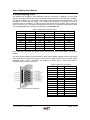
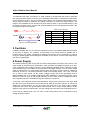
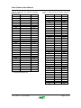
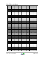
PRELIMINARY
Video Platform User Manual
V2.0, Rev. 1.1 (5/25/2005)
•
1 Overview
This datasheet describes a compact
configurable platform, capable of real time
video processing, based on a board
equipped with a FPGA. The board has
been designed to meet the high demanding
characteristics
of
real
time
video
processing. This inexpensive and costeffective platform can be easily used and
configured for different types of algorithms
and applications. It provides interfaces with
a digital camera and with an output video
peripheral for video display. It is also
equipped with a standard bus connector to
allow debug or stream data input/output or
to attach expansion modules. In fig. 1 is
presented the block diagram of the
platform.
VGA
Generic Connector
Camera Connector
Figure 1: Block diagram of the platform.
2 Features
The developed board presents the following
main features:
• Xilinx Spartan3 XC3S400 FPGA as the
processing core with:
o 400K system gates,
o 288Kb of RAM in 16 blocks,
o Sixteen 18-bit multipliers,
o Fast carry look-ahead logic,
o JTAG configuration or through
Serial PROM;
•
•
•
•
•
Xilinx XCF02S serial configuration flash
PROM (On-board FPGA boot);
Two 100-mil spaced, right angle DIP,
expansion connectors:
o “Camera Connector”: 32-pin header
providing 25 I/O pins, including two
Global Clock inputs, supports
several camera modules from
Omnivision,
o ”Generic I/O Connector”: 40-pin
socket providing 37 I/O pins,
including
four
GCLK
inputs,
supports
several
expansion
modules provided by Diligent;
VGA true color display port, with three
20MHz conversion rate video DACs;
On-board user interface: eight LEDs,
one 4-way slide switch, two push
buttons;
50MHz HCMOS 3.3V oscillator;
Three 3A power regulators (1.2 V, 2.5V
and 3.3V) and one 1.5A, 5V power
regulator.
3 Platform Description
The employed FPGA has sixteen
embedded 18-bit multipliers, fast carry lookahead logic and a total of 400K system
gates. This gives the developer enough
resources to perform video processing. The
development can be performed by
designing the circuits in VHDL, using the
free ISE WebPACK software tool from
Xilinx.
To provide the interface with a standard
VGA monitor, this design employs three
high speed video DACs capable of a
conversion rate up to 30MHz. These
devices generate the red (R), green (G),
blue (B), analog color signals require for the
VGA interface. Impedance adaptation is
ensured using a triple video buffer.
Contact: INESC I&D, Signal Processing Systems Group (SiPS), Rua Alves Redol, 9, 1000-029 Lisboa,
Portugal, +351 21 3100378, +351 21 3145843, http://sips.inesc-id.pt/videodevkit
Document: VPv20r11-01
Video Platform User Manual
32
31
39
40
Camera Connector
2
1
Generic Connector
OSC
1
2
VGA Connector
The board has been designed to be
compatible with several expansion modules,
like the provided by Digilent. The employed
expansion connectors use standard 100mil
spacing and can easily be found in common
distributors.
These
connectors
make
available: I/O pins, one or more supply
voltages and a reference ground signal.
Furthermore, as currently CMOS sensors
are capable of relatively good image quality,
the board was equipped with a connector
capable of receiving several development
camera modules from Omnivision. Since the
development modules can be equipped with
different image sensors, the voltage level
applied to “Camera Connector” can be
configured. With this platform it is provided a
simple VHDL description of an image
capture module with the corresponding
camera register configuration module.
Table 1 presents a summary of all the
signals routed on the Video Board. A more
detailed description of these circuits can be
found in the following sections. Figure 2
presents a simplified layout of the
components in the Video Board, which has
been implemented with a four layers; the two
internal corresponding to power/ground
planes.
Figure 2: Simplified layout of the Video Board.
Power Supplies:
• VCCu – Unregulated power supply
voltage;
• VCCo – 3.3V, routed on a PCB plane,
employs a 3A PWM regulator, I/O
supply voltage for the FPGA;
• VCCaux – 2.5V auxiliary supply, required
for the FPGA and for the camera
expansion connector, also uses a 3A
PWM regulator;
• VCCint – 1.2V core supply, provides the
supply voltage to the FPGA;
• VCC – 5V provides power to the DACs
or for the “Camera Connector”,
maximum of 1.5A;
• GND – System ground to all devices
except the analog ground of the DACs.
Video Port:
• DR0-DR7 – Digital red data signal bus
that connect to a DAC;
• DG0-DG7 – Digital green data signal
bus that connect to a DAC;
• DB0-DB7 – Digital blue data signal bus
that connect to a DAC;
• CLK_dac – Clock signal for the DACs;
• HS – Horizontal VGA synchronization;
• VS – Vertical VGA synchronization;
• RGB – Analog VGA color channels.
On-board Devices:
• LED0-LED7 – User controllable LEDs;
• BTN0-BTN3 – User controllable slide
switch inputs;
• BTN4-BTN5 – User controllable push
button inputs;
• Power Fail – Overvoltage condition
LED;
• Power Good – Normal supply status
LED;
• CLK – HCMOS oscillator connected to
GCLK5;
Expansion Connectors:
• C01-C32 – Signals that connect the
“Camera Connector” to the FPGA and
to the power supplies;
• G04-G40 – Signal bus that connects
the FPGA to the “Generic I/O
Connector”.
• VTO – Analog Video signal output;
Table 1: Video Board signal definitions.
V2.0, Rev. 1.1 (5/25/2005)
Page 2 of 8
Video Platform User Manual
4 VGA Display Port
The display port is based in three separate 8-bit DAC converters, TLC5602C, one per RGB
channel. This DAC presents low power consumption and a maximum conversion rate of 20MHz.
The signal conditioning for VGA port is performed using high speed video buffers with a 75Ω
resistance in series with the output. The voltage level required for powering the DAC is
generated using a TPS78601, an ultra low-noise, low-dropout linear regulator with a maximum
output current of 1.5A. The FPGA pin assignments for the tree converters are presented in table
2, the clock signal for the all DACs is provided by the FPGA pin 140.
Table 2: FPGA pins for the video DACs.
Data Red
FPGA PIN
Function
106
DR0 (LSB)
107
DR1
108
DR2
109
DR3
111
DR4
113
DR5
114
DR6
115
DR7 (MSB)
Data Green
FPGA PIN
Function
116
DG0 (LSB)
117
DG1
119
DG2
120
DG3
122
DG4
123
DG5
124
DG6
125
DG7 (MSB)
Data Blue
FPGA PIN
Function
126
DB0 (LSB)
128
DB1
130
DB2
131
DB3
132
DB4
133
DB5
135
DB6
137
DB7 (MSB)
Note: when using this video port please ensure that the clock input of video DACs is lower than
20MHz.
The three analog voltage level generated by these DACs (RGB), together with the Horizontal
Sync (HS) and the Vertical Sync (HS) are connected to a PCB mounted, 15-pin sub-HD socket
(standard VGA). Figure 3 describes the mapping of these pins in socket and table 3
summarizes the function of each pin.
Table 3: VGA socket pin mapping.
Figure 3: VGA socket pin description.
V2.0, Rev. 1.1 (5/25/2005)
FPGA PIN
138
139
-
Number
1
2
3
4
5
6
7
8
9
10
11
12
13
14
15
VGA
analog Red
analog Green
analog Blue
N. C.
Ground
Ground
Ground
Ground
N. C.
Ground
N. C.
N. C.
HS
VS
N. C.
Page 3 of 8
Video Platform User Manual
To implement this video out interface, a VHDL module is provided with the board to generate
the synchronization signals necessary for a standard VGA monitor. The adopted configuration
uses a resolution of 640 x 480 and a refresh rate of 60Hz. The provided implementation uses a
simple stage machine to generate the signals necessary to control the image display. The
image to be visualized can be stored into a frame memory block or be provided directly by the
processing modules. Figure 4 shows the temporal diagram of the VGA signals and Table 4 the
necessary timings for the signals.
Table 4: VGA Timings.
Figure 4: VGA timing diagram.
Symbol
Parameter
VS
HS
TS
Period
16.7 ms
32 µs
Tdisp
Display time
15.36 ms 25.6 µs
Tpw
Sync pulse width 64 µs
3.84 µs
Tfp
Sync front porch 320 µs
640 ns
Tbp
Sync back porch 928 µs 1.92 µs
5 Oscillator
A 50MHz oscillator with a 3.3V maximum amplitude is used. This HCMOS SMD device presents
an accuracy of 50ppm. The oscillator is connected to one GCLK FPGA pin (P181) and is
located close to the FPGA. Oscillators for different frequencies can be employed by request.
Using the DCMs (Digital Clock Managers) available in the Startan 3 FPGA other frequencies
can also be synthesized.
6 Power Supply
This board requires a power supply with an output voltage within the range of 5V to 6V DC. The
input voltage is monitored using a MAX4841, which provides overvoltage protection up to 28V.
If the unregulated input voltage is above 5.8V the MAX4841 disables a FET transistor isolating
the remaining circuit. The “PWR Fail” led indicates overvoltage condition. The DC power socket
must be connected to a 2.1mm female center-positive plug and the supply must be capable of
delivering at least 1A. The board generates a total of four voltage levels, 1.2V, 2.5V, 3.3V and
5V. In order to save power, all the supply voltages except the 5V are generated using a
MAX1830/MAX1831 a low voltage PWM (Pulse Width Modulation), step-down regulator, which
delivers a current of up to 3A with a peak efficiency of 94%. Some of these voltages, as well as
the unregulated input are available through the expansion connectors.
To achieve a more efficient PDS (Power Distribution System) this board uses a four layer PCB
with the inner layers dedicated to ground and power. Most of the power plane is at 3.3V but is
divided into several islands, one for each DAC and more two for the other supply voltages
required for the FPGA. The ground plane is also divided, but in a more simple manner. All the
digital circuitry shares the same plane, only the analog part of the DACs has a separate ground.
All the I/O pin operate with 3.3V, but some of the FPGA banks can be connected to other
voltage levels by request.
V2.0, Rev. 1.1 (5/25/2005)
Page 4 of 8
Video Platform User Manual
7 FPGA Configuration
The FPGA can be configured using a six pin JTAG header; fig. 5 shows the function of each pin
in the connector. The header can be connected to a standard JTAG programming cable
(Digilent JTAG3), the Vcc pin is connected to the 3.3V supply voltage.
It also employs the XCF02S serial configuration flash PROM to store FPGA configuration data.
Using this design, the FPGA can automatically boot from the on-board PROM whenever the
power is applied. The configuration of the PROM is also done through the JTAG header.
.
.
.
Control
Switches
.
RGB
.
.
Figure 5: JTAG connector pin order.
8 On-board User Interface
The slide switches can be used to connect either VCCo or GND to the FPGA pins.The slide
switch in the OFF position pulls the FPGA pin to ground and in the ON will go high. The output
of the push button is normally pulled to VCCo, when pressed is pulled to ground. No active
debounce circuit was employed in either interface.
The board also provides 8 LEDs as output circuits and those LEDs are driven directly from the
FPGA pins. The LEDs are accessible through the pins presented in table 7 and are active high.
Table 6: FPGA pins for the slide switches
and the push buttons.
FPGA PIN Function
PIN num
156
BTN0
1
155
BTN1
2
154
BTN2
3
152
BTN3
4
150
BTN4
149
BTN5
-
V2.0, Rev. 1.1 (5/25/2005)
Table 7: FPGA pins for the leds.
FPGA PIN Function
19
LED0
18
LED1
16
LED2
15
LED3
13
LED4
12
LED5
11
LED6
10
LED7
Page 5 of 8
Video Platform User Manual
9 Image Capture
The board is pin compatible several digital camera modules from Omnivision like the camera
module based on the OV7620 CMOS image sensor or other modules with more recent sensors
like the OV9650. All camera functions can be configured using a serial data transmission
protocol, SCCB, which is a simplified version of the Philips I2C protocol. A VHDL
implementation of this protocol is supplied, the desired register values are provided by a simple
VHDL ROM like description. Considering a camera module with the OV9650 sensor, it can be
programmed to capture frames in SXGA, VGA, QVGA and other specific formats or other
programmed format. Frame synchronization is performed by detecting a high pulse in the
vertical sync (VSYN) signal and a new line occurs with a low pulse on the horizontal reference
(HREF) signal, moreover, the camera also provides the pixel clock (PCLK) signal. Figure 6
shows the temporal diagrams of those signals.
Figure 6: Camera module sync signals.
The pixels information is updated every falling edge of the PCLK signal, which means that pixel
information can be read on the rising edge of PCLK, the VHDL description of this module is
provided.
10 Expansion Connectors
This board provides two expansion connectors; both can provide supply power to an expansion
module. The pin arrangement is not equal for the two connectors. As the ”Camera Connector”
must receive data from a digital camera the pin arrangement must be the same than for the
camera module. The power pins of this connector can be configured through JP1 to be 5V or
2.5V, depending on the camera module. Both connectors are close to the FPGA, thus these
connectors will exhibit a small signal delay, and high data transfer rates.
RGB
8-bit DACs
JTAG
24
PROM
XILINX
SPARTAN
XC3S400
25
37
Generic Connector
Camera Connector
All the available I/O signals from the FPGA
can be seen in fig. 7, and the mapping of all
the pins is shown in table 10.
VGA
Table 6 shows the pin mapping between
the FPGA I/O and the ”Camera Connector”.
There is also a two pin header that provides
the analog output video signal, if the
employed module provides this output.
Table 7 shows the FPGA pins for the
”Generic I/O Connector” expansion slot.
Control
Switches
LEDs
8
6
Figure 7: FPGA available I/O signals.
V2.0, Rev. 1.1 (5/25/2005)
Page 6 of 8
Video Platform User Manual
Table 8: FPGA pins for camera connector
expansion slot.
FPGA PIN
Function
178
176
180*
182
187
185
190
189
194
191
197
196
198
199
GND
200
GND
183*
184*
Vccaux/Vcc **
GND
Vccaux/Vcc **
203
204
205
2
3
4
5
7
GND
VTO
* GCLK pin
** Configured through JP1
V2.0, Rev. 1.1 (5/25/2005)
Number
C01
C02
C03
C04
C05
C06
C07
C08
C09
C10
C11
C12
C13
C14
C15
C16
C17
C18
C19
C20
C21
C22
C23
C24
C25
C26
C27
C28
C29
C30
C31
C32
Table 9: FPGA pins for the generic expansion
slot.
FPGA PIN
52
101
102
97
100
95
96
93
94
90
92
86
87
83
85
80*
81
78
79*
76*
77*
72
74
68
71
65
67
63
64
61
62
57
58
50
48
46
48
* GCLK pin
Function
GND
Vccu
Vcco
Number
G01
G02
G03
G04
G05
G06
G07
G08
G09
G10
G11
G12
G13
G14
G15
G16
G17
G18
G19
G20
G21
G22
G23
G24
G25
G26
G27
G28
G29
G30
G31
G32
G33
G34
G35
G36
G37
G38
G39
G40
Page 7 of 8
Video Platform User Manual
Table 10: Video Board FPGA pin assignment.
FPGA PIN
1
2
3
4
5
6
7
8
9
10
11
12
13
14
15
16
17
18
19
20
21
22
23
24
25
26
27
28
29
30
31
32
33
34
35
36
37
38
39
40
41
42
43
44
45
46
47
48
49
50
51
52
Number
GND
C26
C27
C28
C29
Vcco
C30
GND
N. C.
LED7
LED6
LED5
LED4
GND
LED3
LED2
Vccaux
LED1
LED0
N. C.
N. C.
N. C.
Vcco
N. C.
GND
N. C.
N. C.
N. C.
N. C.
GND
N. C.
Vcco
N. C.
N. C.
N. C.
N. C.
N. C.
Vccaux
N. C.
N. C.
GND
N. C.
N. C.
N. C.
N. C.
G39
GND
G38
Vcco
G37
N. C.
G04
FPGA PIN
53
54
55
56
57
58
59
60
61
62
63
64
65
66
67
68
69
70
71
72
73
74
75
76*
77*
78
79*
80*
81
82
83
84
85
86
87
88
89
90
91
92
93
94
95
96
97
98
99
100
101
102
103
104
Number
GND
GND
GND
GND
G35
G36
GND
Vcco
G33
G34
G31
G32
G29
GND
G30
G27
Vccaux
Vccint
G28
G25
Vcco
G26
GND
G23
G24
G21
G22
G19
G20
GND
G17
Vcco
G18
G15
G16
Vccint
Vccaux
G13
GND
G14
G11
G12
G09
G10
G07
Vcco
GND
G08
G05
G06
DONE
CCLK
FPGA PIN
105
106
107
108
109
110
111
112
113
114
115
116
117
118
119
120
121
122
123
124
125
126
127
128
129
130
131
132
133
134
135
136
137
138
139
140
141
142
143
144
145
146
147
148
149
150
151
152
153
154
155
156
Number
GND
DR0 (LSB)
DR1
DR2
DR3
Vcco
DR4
GND
DR5
DR6
DR7 (MSB)
DG0 (LSB)
DG1
GND
DG2
DG3
Vccaux
DG4
DG5
DG6
DG7 (MSB)
DB0 (LSB)
Vcco
DB1
GND
DB2
DB3
DB4
DB5
GND
DB6
Vcco
DB7 (MSB)
HS
VS
CLK_dac
N. C.
Vccaux
N. C.
N. C.
GND
N. C.
N. C.
N. C.
BTN5
BTN4
GND
BTN3
Vcco
BTN2
BTN1
BTN0
FPGA PIN
157
158
159
160
161
162
163
164
165
166
167
168
169
170
171
172
173
174
175
176
177
178
179
180*
181*
182
183*
184*
185
186
187
188
189
190
191
192
193
194
195
196
197
198
199
200
201
202
203
204
205
206
207
208
Number
GND
TDO
TCK
TMS
N. C.
N. C.
GND
Vcco
N. C.
N. C.
N. C.
N. C.
N. C.
GND
N. C.
N. C.
Vccaux
Vccint
N. C.
C02
Vcco
C01
GND
C03
CLK
C04
C18
C19
C06
GND
C05
Vcco
C08
C07
C10
Vccint
Vccaux
C09
GND
C12
C11
C13
C14
C16
Vcco
GND
C23
C24
C25
GND
PROG_B
TDI
* GCLK input
V2.0, Rev. 1.1 (5/25/2005)
Page 8 of 8